Cyclone III Development Board Reference Manual · Cyclone III Development Board Reference Manual...
90
101 Innovation Drive San Jose, CA 95134 www.altera.com Cyclone III Development Board Reference Manual Document Date: March 2008
Transcript of Cyclone III Development Board Reference Manual · Cyclone III Development Board Reference Manual...
101 Innovation DriveSan Jose, CA 95134www.altera.com
Cyclone III Development Board
Reference Manual
Document Date: March 2008
Copyright © 2008 Altera Corporation. All rights reserved. Altera, The Programmable Solutions Company, the stylized Altera logo, specific device des-ignations, and all other words and logos that are identified as trademarks and/or service marks are, unless noted otherwise, the trademarks andservice marks of Altera Corporation in the U.S. and other countries. All other product or service names are the property of their respective holders. Al-tera products are protected under numerous U.S. and foreign patents and pending applications, maskwork rights, and copyrights. Altera warrantsperformance of its semiconductor products to current specifications in accordance with Altera's standard warranty, but reserves the right to makechanges to any products and services at any time without notice. Altera assumes no responsibility or liability arising out of the ap-plication or use of any information, product, or service described herein except as expressly agreed to in writing by AlteraCorporation. Altera customers are advised to obtain the latest version of device specifications before relying on any published in-formation and before placing orders for products or services.
ii Development Board Version 1.0.0 Altera CorporationCyclone III Development Board Reference Manual March 2008
Part Number MNL-01029-1.1
Altera Corporation iiiPreliminary
Contents
About this Manual Revision History ......................................................................................................................................... vHow to Contact Altera ............................................................................................................................... vTypographic Conventions....................................................................................................................... vi
Chapter 1. Overview Introduction............................................................................................................................................. 1-1General Description................................................................................................................................ 1-1
Board Component Blocks................................................................................................................. 1-2Block Diagram ................................................................................................................................... 1-4Handling the Board........................................................................................................................... 1-4
Chapter 2. Board Components Introduction............................................................................................................................................. 2-1Board Overview...................................................................................................................................... 2-1Featured FPGA (U20)............................................................................................................................. 2-5
I/O and Clocking Resources ........................................................................................................... 2-6MAX II CPLD .......................................................................................................................................... 2-7Configuration, Status, and Setup Elements ...................................................................................... 2-17
Configuration................................................................................................................................... 2-17FPGA Programming Over USB ............................................................................................... 2-17FPGA Programming from Flash Memory.............................................................................. 2-19Flash Programming over USB Interface ................................................................................. 2-19
Status Elements................................................................................................................................ 2-20Board Specific LEDs .................................................................................................................. 2-20Power Display ............................................................................................................................ 2-21
Setup Elements ................................................................................................................................ 2-21JTAG Control DIP Switch ......................................................................................................... 2-22MAX II Device Control DIP Switch......................................................................................... 2-22System Reset & Configuration Switches ................................................................................ 2-23POWER SELECT Rotary Switch .............................................................................................. 2-24PGM CONFIG SELECT Rotary Switch................................................................................... 2-25Speaker Header (J5) ................................................................................................................... 2-26
Clocking Circuitry ................................................................................................................................ 2-26Cyclone III FPGA Clock Inputs..................................................................................................... 2-26Cyclone III FPGA Clock Outputs.................................................................................................. 2-27Oscillators ......................................................................................................................................... 2-30
General User Interfaces........................................................................................................................ 2-30User-Defined Push Button Switches............................................................................................. 2-30User-Defined DIP Switches ........................................................................................................... 2-31User-Defined LEDs ......................................................................................................................... 2-32
iv Altera CorporationPreliminary
Contents Stratix Device Handbook, Volume 1
General User-Defined LEDs..................................................................................................... 2-32HSMC User-Defined LEDs....................................................................................................... 2-33DDR2 User-Defined LEDs ........................................................................................................ 2-34
7-Segment Displays......................................................................................................................... 2-35User 7-Segment Display............................................................................................................ 2-35Power 7-Segment Display......................................................................................................... 2-37
LCD Displays ................................................................................................................................... 2-37Character LCD (J4)..................................................................................................................... 2-37Graphics LCD (J13) .................................................................................................................... 2-39
Communication Ports & Interface Cards .......................................................................................... 2-45USB 2.0 MAC/PHY......................................................................................................................... 2-4510/100/1000 Ethernet..................................................................................................................... 2-47High Speed Mezzanine Cards ....................................................................................................... 2-51
On-Board Memory ............................................................................................................................... 2-55DDR2 SDRAM ................................................................................................................................. 2-55SRAM ................................................................................................................................................ 2-58Flash Memory .................................................................................................................................. 2-62
Power Supply ........................................................................................................................................ 2-65Power Measurement ............................................................................................................................ 2-67Statement of China-RoHS Compliance ............................................................................................. 2-69
Altera Corporation vPreliminary
About this Manual
Revision History The table below displays the revision history for the chapters in this reference manual.
This reference manual provides comprehensive information about the Altera® Cyclone® III development board.
How to Contact Altera
For the most up-to-date information about Altera products, refer to the following table.
Chapter Date Version Changes Made
All October 2007 1.0.0 ● First publication.
2 March 2008 1.1.0 ● Added schematic information to, revised I/O standard terminology, and added data bit information to the HSMC Port A and Port B tables.
● Added schematic information to and revised I/O standard terminology to the DDR 2 interface I/O table.
● Added schematic information to and revised I/O standard terminology to the Ethernet PHY I/O table.
● Added schematic information to and revised I/O standard terminology to the flash memory I/O table.
● Added schematic information to and revised I/O standard terminology to the graphics LCD table.
● Added schematic information to and revised I/O standard terminology to the SRAM table.
● Updated power measurement table. ● Updated flash memory map table.● Added flash memory map definition table.
Information Type Contact Note (1)
Technical support www.altera.com/mysupport/
Technical training www.altera.com/training/
Technical training services [email protected]
Product literature www.altera.com/literature
Product literature services [email protected]
FTP site ftp.altera.com
Note to table:(1) You can also contact your local Altera sales office or sales representative.
vi Altera CorporationPreliminary
How to Contact Altera Cyclone FPGA Device Handbook
Typographic Conventions
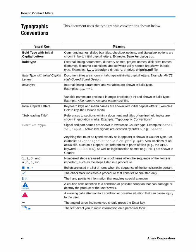
This document uses the typographic conventions shown below.
Visual Cue Meaning
Bold Type with Initial Capital Letters
Command names, dialog box titles, checkbox options, and dialog box options are shown in bold, initial capital letters. Example: Save As dialog box.
bold type External timing parameters, directory names, project names, disk drive names, filenames, filename extensions, and software utility names are shown in bold type. Examples: fMAX, \qdesigns directory, d: drive, chiptrip.gdf file.
Italic Type with Initial Capital Letters
Document titles are shown in italic type with initial capital letters. Example: AN 75: High-Speed Board Design.
Italic type Internal timing parameters and variables are shown in italic type. Examples: tPIA, n + 1.
Variable names are enclosed in angle brackets (< >) and shown in italic type. Example: <file name>, <project name>.pof file.
Initial Capital Letters Keyboard keys and menu names are shown with initial capital letters. Examples: Delete key, the Options menu.
“Subheading Title” References to sections within a document and titles of on-line help topics are shown in quotation marks. Example: “Typographic Conventions.”
Courier type Signal and port names are shown in lowercase Courier type. Examples: data1, tdi, input. Active-low signals are denoted by suffix n, e.g., resetn.
Anything that must be typed exactly as it appears is shown in Courier type. For example: c:\qdesigns\tutorial\chiptrip.gdf. Also, sections of an actual file, such as a Report File, references to parts of files (e.g., the AHDL keyword SUBDESIGN), as well as logic function names (e.g., TRI) are shown in Courier.
1., 2., 3., anda., b., c., etc.
Numbered steps are used in a list of items when the sequence of the items is important, such as the steps listed in a procedure.
■ ● • Bullets are used in a list of items when the sequence of the items is not important.
v The checkmark indicates a procedure that consists of one step only.
1 The hand points to information that requires special attention.
c A caution calls attention to a condition or possible situation that can damage or destroy the product or the user’s work.
w A warning calls attention to a condition or possible situation that can cause injury to the user.
r The angled arrow indicates you should press the Enter key.
f The feet direct you to more information on a particular topic.
Altera Corporation Reference Manual 1–1March 2008 Preliminary
1. Overview
Introduction This document describes the hardware features of the Cyclone® III development board, including detailed pinout information to enable designers to create custom FPGA designs that interface with all components of the board.
f For information on setting up and powering up the Cyclone III development board and using the kit’s demo software, please refer to the Cyclone III Development Kit User Guide.
General Description
The Cyclone® III development board provides a hardware platform for developing and prototyping low-power, high-volume, feature-rich designs as well as to demonstrate the Cyclone III device’s on-chip memory, embedded multipliers, and the Nios® II embedded soft processor.
With up to 4-Mbits of embedded memory and 288 embedded 18-bit x 18-bit multipliers, the Cyclone III device supplies an abundance of internal memory while also providing external support for high-speed, low-latency memory access via dual-channel DDR SDRAM and low-power SRAM.
Built on TSMC’s 65-nm low-power process technology, Cyclone III devices are designed to provide low static and dynamic power consumption. Additionally, with the support of the Quartus® II software’s PowerPlay technology, designs are automatically optimized for power consumption. Therefore, the Cyclone III development board provides a power-optimized, integrated solution for memory-intensive, high-volume applications.
Accordingly, the Cyclone III development board is especially suitable for wireless, video and image processing, and other high-bandwidth, parallel processing applications. Through the use of Altera®-provided video and image intellectual property (or other MegaCore® functions) and board expansion connectors, you can enable the inter-operability of the Cyclone III device, allowing application-specific customization of the development board.
f For more information about the Altera Video and Image Processing Suite MegaCore functions, refer to the Video and Image Processing Suite User Guide.
1–2 Reference Manual Altera CorporationCyclone III Development Board March 2008
General Description
To get you started, Altera provides application-specific design examples. The pre-built and tested design examples allow you to:
■ Create a Cyclone III FPGA design in one hour■ View Cyclone III FPGA power measurement examples■ Design a 32-bit soft processor system inside the Cyclone III FPGA in
one hour
The Cyclone III development board has the following main features:
■ Higher logic density to implement more functions and features■ More embedded memory for high-bandwidth applications■ Expandable through two Altera High Speed Mezzanine Card
(HSMC) connectors■ 256-MB of dual channel DDR2 SDRAM with a 72-bit data width■ Supports high-speed external memory interfaces including
dual-channel DDR SDRAM and low-power SRAM ■ Four user push-button switches■ Eight user LEDs■ Power consumption display
The Cyclone III development board provides the following advantages:
■ Unique combination of low-cost, low-power Cyclone III FPGA that supports high-volume, memory-intensive designs
■ Highest multiplier-to-logic ratio FPGA in the industry■ Lowest cost, density- and power-optimized FPGA■ Quartus II development software’s power optimization tools
Board Component Blocks
The board features the following major component blocks:
■ 780-pin Altera Cyclone III EP3C120 FPGA in a BGA package● 119K logic elements (LEs)● 3,888 Kbits of memory● 288 18 x 18 multiplier blocks● Four phase locked loops (PLLs)● 20 global clock networks● 531 user I/Os● 1.2 V core power
■ 256-pin Altera MAX® II EPM2210G CPLD in a FineLine Ball Grid Array (FBGA) package● 1.8 V core power
■ On-board memory● 256 MB dual-channel DDR2 SDRAM● 8 MB SRAM
Altera Corporation Reference Manual 1–3March 2008 Cyclone III Development Board
Overview
● 64 MB flash memory■ FPGA configuration circuitry
● MAX II CPLD and flash passive serial configuration● On-board USB-Blaster™ circuitry using the Quartus II
Programmer■ On-board clocking circuitry
● Two clock oscillators to support Cyclone III device user logic• 50-MHz• 125-MHz
● 80 I/O, 6 clocks, SMBus, and JTAG● SMA connector for external clock input and output
■ General user and configuration interfaces● LEDs/displays:
• Eight user LEDs• One transmit/receive LED (TX/RX) per HSMC interface• One configuration done LED• Ethernet LEDs• User 7-segment display• Power consumption display
● Memory activity LEDs:• SRAM• FLASH• DDR2 Top• DDR2 Bottom
● Push-buttons:• One user reset push-button (CPU reset)• Four general user push-buttons• One system reset push-button (user configuration)• One factory push-button switch (factory configuration)
● DIP switches:• One MAX control DIP switch• One JTAG control switch• Eight user DIP switches
● Speaker header■ Displays
● 128 x 64 graphics LCD● 16 x 2 line character LCD
■ Power supply● 14 V - 20 V DC input● On-board power measurement circuitry● Up to 19.8 W per HSMC interface
■ Mechanical● 6”x 8” board● Bench-top design
1–4 Reference Manual Altera CorporationCyclone III Development Board March 2008
Handling the Board
Block Diagram
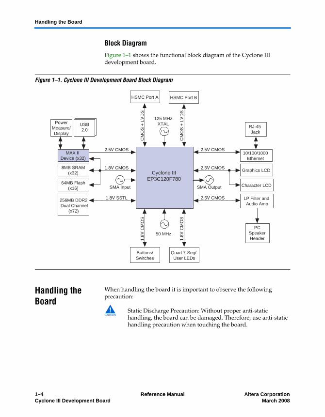
Figure 1–1 shows the functional block diagram of the Cyclone III development board.
Figure 1–1. Cyclone III Development Board Block Diagram
Handling the Board
When handling the board it is important to observe the following precaution:
c Static Discharge Precaution: Without proper anti-static handling, the board can be damaged. Therefore, use anti-static handling precaution when touching the board.
CM
OS
+ L
VD
S
Cyclone IIIEP3C120F780
125 MHzXTAL
SMA Input
MAX II Device (x32)
2.5V CMOS
1.8V CMOS
PowerMeasure/Display
HSMC Port A
CM
OS
+ L
VD
S
HSMC Port B
8MB SRAM(x32)
64MB Flash(x16)
256MB DDR2 Dual Channel
(x72)
USB2.0
1.8V
CM
OS
50 MHz
Buttons/Switches
1.8V
CM
OS
Quad 7-Seg/ User LEDs
1.8V SSTL
SMA Output
10/100/1000Ethernet
2.5V CMOS
2.5V CMOS
RJ-45 Jack
Graphics LCD
Character LCD
LP Filter and Audio Amp
2.5V CMOS
PCSpeakerHeader
Altera Corporation March 2008
2. Board Components
Introduction This chapter introduces all the important components on the Cyclone® III development board. Figure 2–1 illustrates all component locations and Table 2–1 describes component features.
The chapter is divided into the following sections:
■ Featured FPGA■ MAX® II CPLD■ Configuration, status, and setup elements■ Clocking circuitry■ General user interfaces■ Communication ports and interface cards■ On-board memory■ Power supply■ Statement of China-RoHS compliance
1 A complete set of board schematics, a physical layout database, and GERBER files for the Cyclone III development board are installed in the Cyclone III Development Kit documents directory.
f For information on powering up the development board and installing the demo software, refer to the Cyclone III Development Kit User Guide.
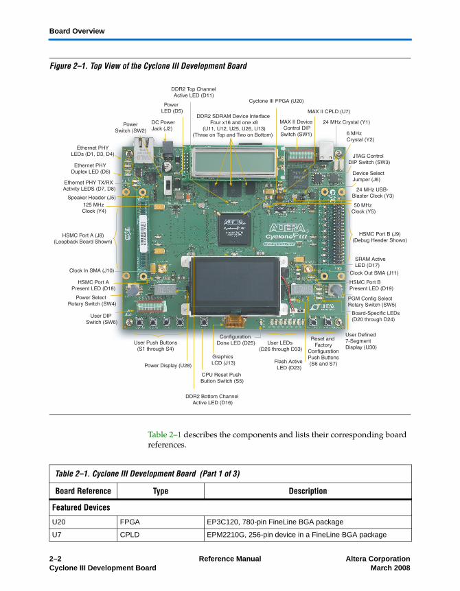
Board Overview This section provides an overview of the Cyclone III development board, including an annotated board image and component descriptions.
Figure 2–1 shows the top view of the Cyclone III development board.
Reference Manual 2–1Preliminary
Board Overview
Figure 2–1. Top View of the Cyclone III Development Board
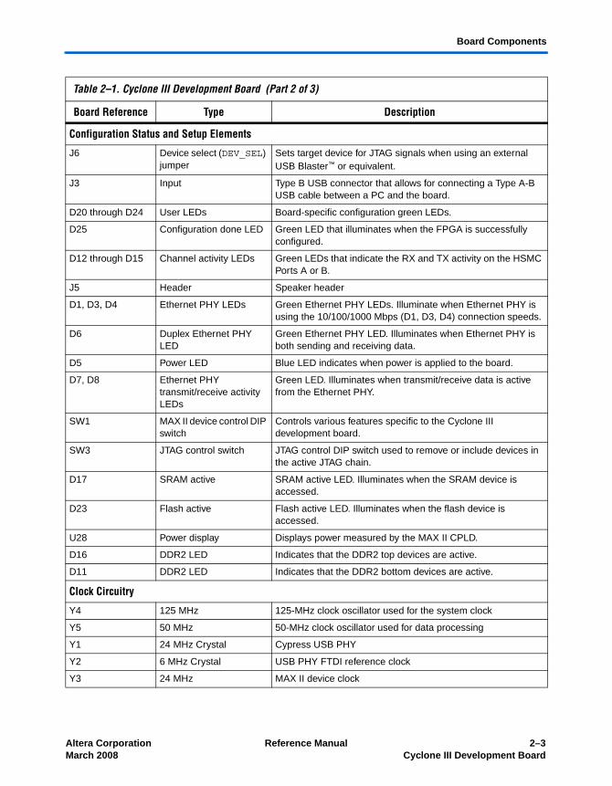
Table 2–1 describes the components and lists their corresponding board references.
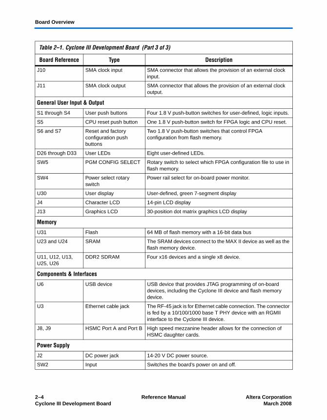
Table 2–1. Cyclone III Development Board (Part 1 of 3)
Board Reference Type Description
Featured Devices
U20 FPGA EP3C120, 780-pin FineLine BGA package
U7 CPLD EPM2210G, 256-pin device in a FineLine BGA package
2–2 Reference Manual Altera CorporationCyclone III Development Board March 2008
Board Components
Configuration Status and Setup Elements
J6 Device select (DEV_SEL) jumper
Sets target device for JTAG signals when using an external USB Blaster™ or equivalent.
J3 Input Type B USB connector that allows for connecting a Type A-B USB cable between a PC and the board.
D20 through D24 User LEDs Board-specific configuration green LEDs.
D25 Configuration done LED Green LED that illuminates when the FPGA is successfully configured.
D12 through D15 Channel activity LEDs Green LEDs that indicate the RX and TX activity on the HSMC Ports A or B.
J5 Header Speaker header
D1, D3, D4 Ethernet PHY LEDs Green Ethernet PHY LEDs. Illuminate when Ethernet PHY is using the 10/100/1000 Mbps (D1, D3, D4) connection speeds.
D6 Duplex Ethernet PHY LED
Green Ethernet PHY LED. Illuminates when Ethernet PHY is both sending and receiving data.
D5 Power LED Blue LED indicates when power is applied to the board.
D7, D8 Ethernet PHY transmit/receive activity LEDs
Green LED. Illuminates when transmit/receive data is active from the Ethernet PHY.
SW1 MAX II device control DIP switch
Controls various features specific to the Cyclone III development board.
SW3 JTAG control switch JTAG control DIP switch used to remove or include devices in the active JTAG chain.
D17 SRAM active SRAM active LED. Illuminates when the SRAM device is accessed.
D23 Flash active Flash active LED. Illuminates when the flash device is accessed.
U28 Power display Displays power measured by the MAX II CPLD.
D16 DDR2 LED Indicates that the DDR2 top devices are active.
D11 DDR2 LED Indicates that the DDR2 bottom devices are active.
Clock Circuitry
Y4 125 MHz 125-MHz clock oscillator used for the system clock
Y5 50 MHz 50-MHz clock oscillator used for data processing
Y1 24 MHz Crystal Cypress USB PHY
Y2 6 MHz Crystal USB PHY FTDI reference clock
Y3 24 MHz MAX II device clock
Table 2–1. Cyclone III Development Board (Part 2 of 3)
Board Reference Type Description
Altera Corporation Reference Manual 2–3March 2008 Cyclone III Development Board
Board Overview
J10 SMA clock input SMA connector that allows the provision of an external clock input.
J11 SMA clock output SMA connector that allows the provision of an external clock output.
General User Input & Output
S1 through S4 User push buttons Four 1.8 V push-button switches for user-defined, logic inputs.
S5 CPU reset push button One 1.8 V push-button switch for FPGA logic and CPU reset.
S6 and S7 Reset and factory configuration push buttons
Two 1.8 V push-button switches that control FPGA configuration from flash memory.
D26 through D33 User LEDs Eight user-defined LEDs.
SW5 PGM CONFIG SELECT Rotary switch to select which FPGA configuration file to use in flash memory.
SW4 Power select rotary switch
Power rail select for on-board power monitor.
U30 User display User-defined, green 7-segment display
J4 Character LCD 14-pin LCD display
J13 Graphics LCD 30-position dot matrix graphics LCD display
Memory
U31 Flash 64 MB of flash memory with a 16-bit data bus
U23 and U24 SRAM The SRAM devices connect to the MAX II device as well as the flash memory device.
U11, U12, U13, U25, U26
DDR2 SDRAM Four x16 devices and a single x8 device.
Components & Interfaces
U6 USB device USB device that provides JTAG programming of on-board devices, including the Cyclone III device and flash memory device.
U3 Ethernet cable jack The RF-45 jack is for Ethernet cable connection. The connector is fed by a 10/100/1000 base T PHY device with an RGMII interface to the Cyclone III device.
J8, J9 HSMC Port A and Port B High speed mezzanine header allows for the connection of HSMC daughter cards.
Power Supply
J2 DC power jack 14-20 V DC power source.
SW2 Input Switches the board’s power on and off.
Table 2–1. Cyclone III Development Board (Part 3 of 3)
Board Reference Type Description
2–4 Reference Manual Altera CorporationCyclone III Development Board March 2008
Board Components
FeaturedFPGA (U20)
The Cyclone III Development Kit features the EP3C120F780 device (U20) in a 780-pin BGA package.
f For more information on Cyclone III devices, refer to the Cyclone III Device Handbook.
Table 2–2 lists the main Cyclone III device features.
Table 2–3 lists the Cyclone III component reference and manufacturing information.
Table 2–4 lists the Cyclone III EP3C120F780C7 device pin count.
Table 2–2. Cyclone III Device Features
Feature Quantity
Logic elements 119,088
Memory (Kbits) 3,888
Multipliers 288
PLLs 4
Global clock networks 20
Table 2–3. Cyclone III Component Reference and Manufacturing Information
Board Reference Description Manufacturer ManufacturingPart Number
Manufacturer Web Site
U20 Memory rich FPGA device
Altera® Corporation EP3C120F780 www.altera.com
Table 2–4. Cyclone III Device Pin Count (Part 1 of 2)
Function I/O Type I/O Count Special Pins
Oscillators and SMAs 1.8 V CMOS 4 Three clock inputs, one output
DDR2 1.8 V SSTL 148 Nine data strobe signal (DQS), 10 VREF
Flash/SRAM/MAX 1.8 V CMOS 78 —
Horizontal bank OCT calibration
1.8 V CMOS 4 2 Rup, 2 Rdn
Altera Corporation Reference Manual 2–5March 2008 Cyclone III Development Board
Featured FPGA (U20)
f For additional information about Altera® devices, go to www.altera.com/products/devices.
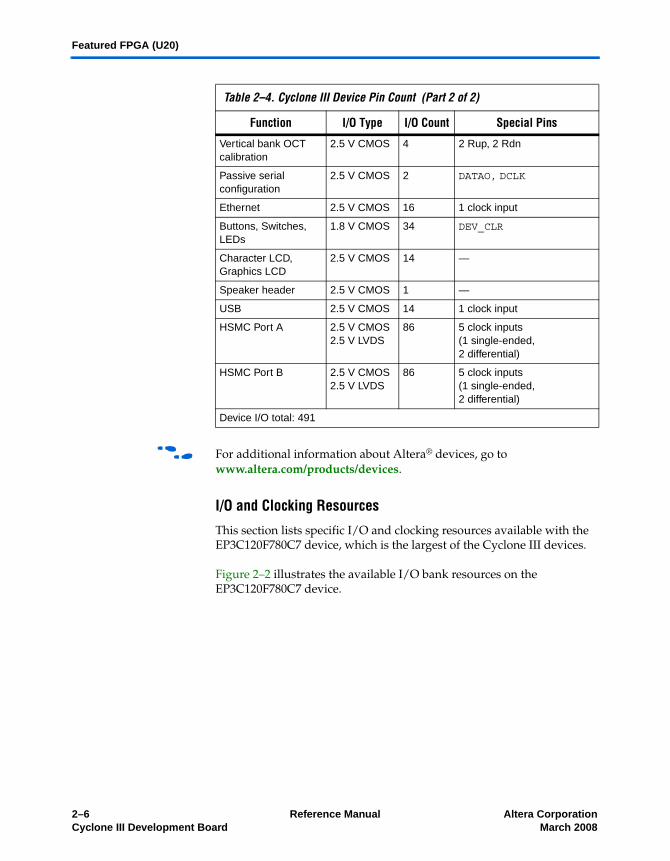
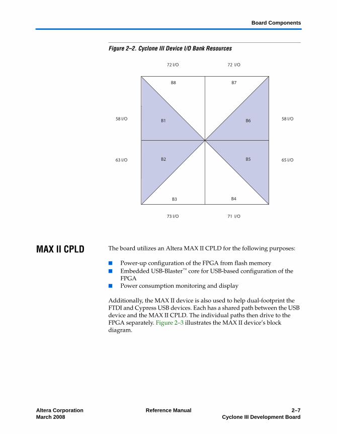
I/O and Clocking Resources
This section lists specific I/O and clocking resources available with the EP3C120F780C7 device, which is the largest of the Cyclone III devices.
Figure 2–2 illustrates the available I/O bank resources on the EP3C120F780C7 device.
Vertical bank OCT calibration
2.5 V CMOS 4 2 Rup, 2 Rdn
Passive serial configuration
2.5 V CMOS 2 DATAO, DCLK
Ethernet 2.5 V CMOS 16 1 clock input
Buttons, Switches, LEDs
1.8 V CMOS 34 DEV_CLR
Character LCD, Graphics LCD
2.5 V CMOS 14 —
Speaker header 2.5 V CMOS 1 —
USB 2.5 V CMOS 14 1 clock input
HSMC Port A 2.5 V CMOS2.5 V LVDS
86 5 clock inputs(1 single-ended, 2 differential)
HSMC Port B 2.5 V CMOS2.5 V LVDS
86 5 clock inputs (1 single-ended, 2 differential)
Device I/O total: 491
Table 2–4. Cyclone III Device Pin Count (Part 2 of 2)
Function I/O Type I/O Count Special Pins
2–6 Reference Manual Altera CorporationCyclone III Development Board March 2008
Board Components
Figure 2–2. Cyclone III Device I/O Bank Resources
MAX II CPLD The board utilizes an Altera MAX II CPLD for the following purposes:
■ Power-up configuration of the FPGA from flash memory■ Embedded USB-Blaster™ core for USB-based configuration of the
FPGA■ Power consumption monitoring and display
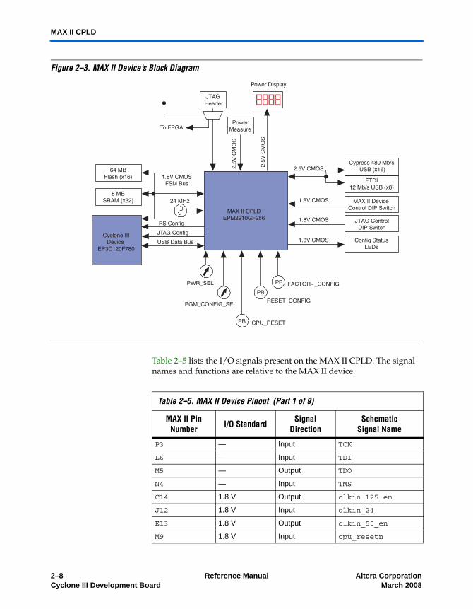
Additionally, the MAX II device is also used to help dual-footprint the FTDI and Cypress USB devices. Each has a shared path between the USB device and the MAX II CPLD. The individual paths then drive to the FPGA separately. Figure 2–3 illustrates the MAX II device’s block diagram.
Altera Corporation Reference Manual 2–7March 2008 Cyclone III Development Board
MAX II CPLD
Figure 2–3. MAX II Device’s Block Diagram
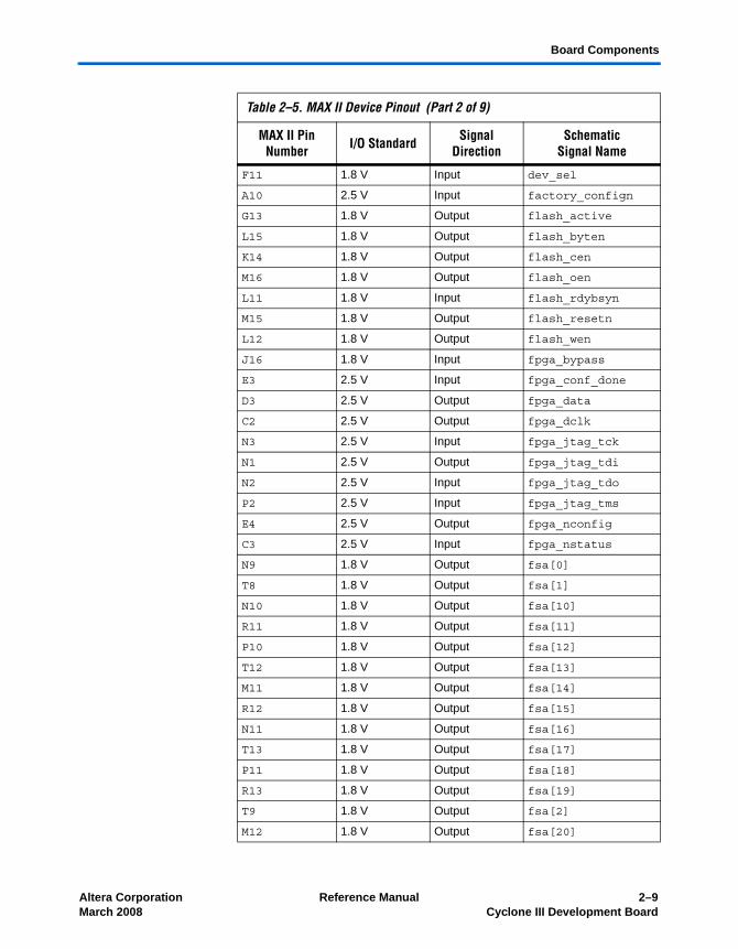
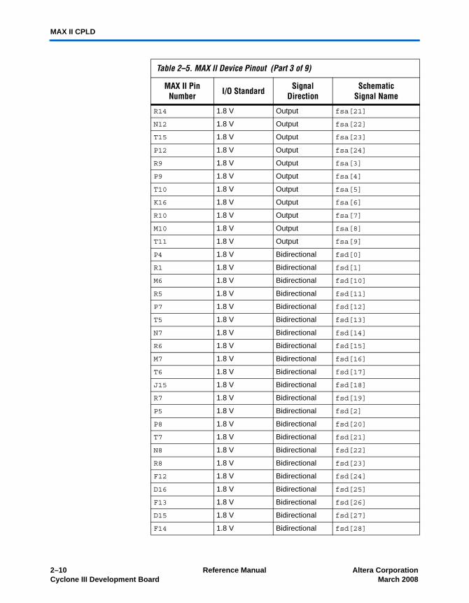
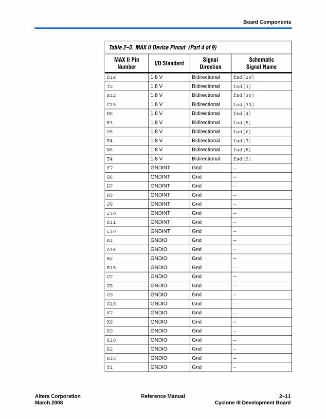
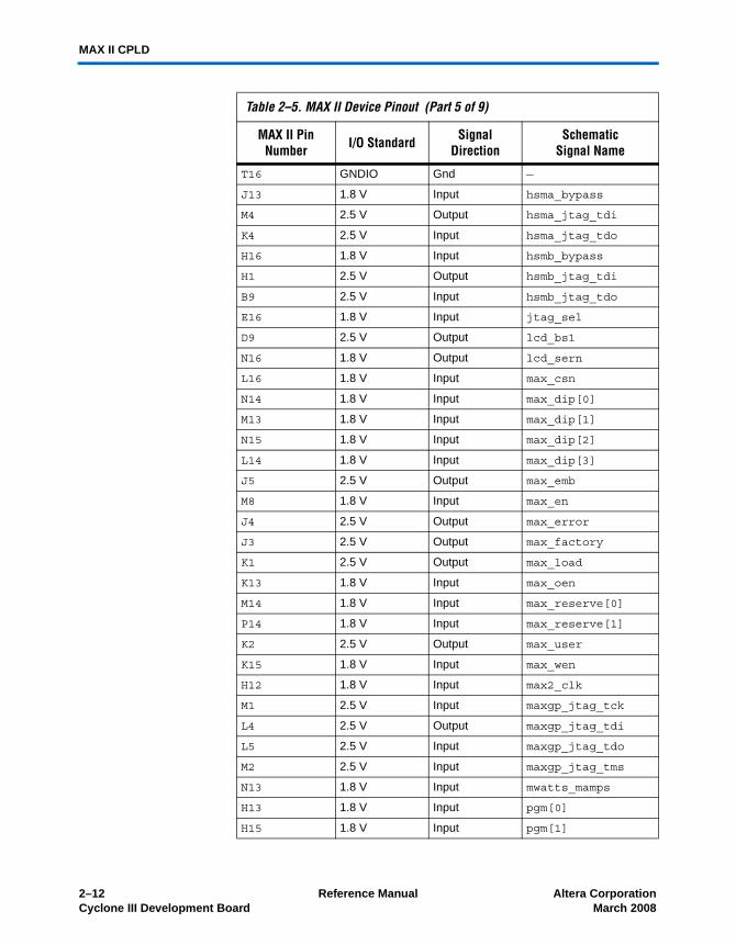
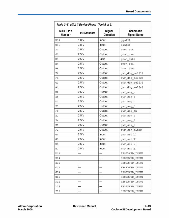
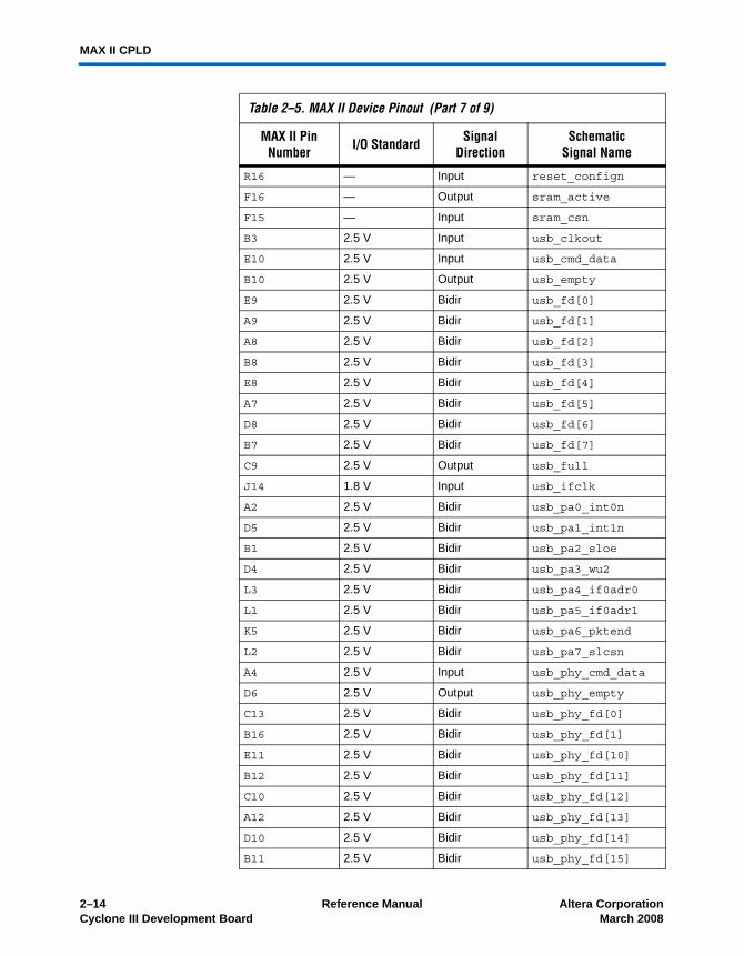
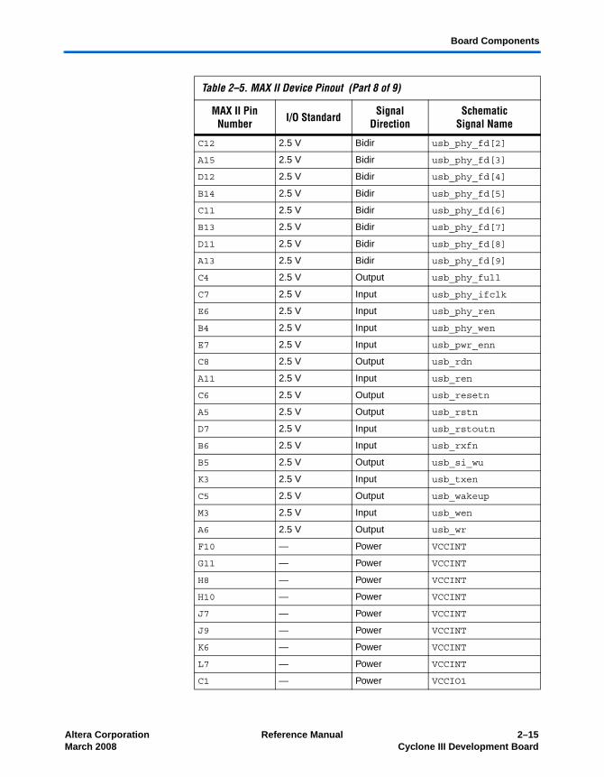
Table 2–5 lists the I/O signals present on the MAX II CPLD. The signal names and functions are relative to the MAX II device.
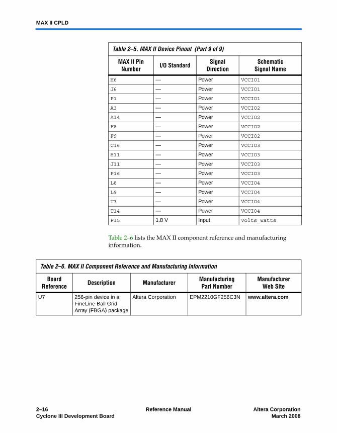
Table 2–5. MAX II Device Pinout (Part 1 of 9)
MAX II Pin Number I/O Standard Signal
DirectionSchematic
Signal Name
P3 — Input TCK
L6 — Input TDI
M5 — Output TDO
N4 — Input TMS
C14 1.8 V Output clkin_125_en
J12 1.8 V Input clkin_24
E13 1.8 V Output clkin_50_en
M9 1.8 V Input cpu_resetn
2–8 Reference Manual Altera CorporationCyclone III Development Board March 2008
Board Components
F11 1.8 V Input dev_sel
A10 2.5 V Input factory_confign
G13 1.8 V Output flash_active
L15 1.8 V Output flash_byten
K14 1.8 V Output flash_cen
M16 1.8 V Output flash_oen
L11 1.8 V Input flash_rdybsyn
M15 1.8 V Output flash_resetn
L12 1.8 V Output flash_wen
J16 1.8 V Input fpga_bypass
E3 2.5 V Input fpga_conf_done
D3 2.5 V Output fpga_data
C2 2.5 V Output fpga_dclk
N3 2.5 V Input fpga_jtag_tck
N1 2.5 V Output fpga_jtag_tdi
N2 2.5 V Input fpga_jtag_tdo
P2 2.5 V Input fpga_jtag_tms
E4 2.5 V Output fpga_nconfig
C3 2.5 V Input fpga_nstatus
N9 1.8 V Output fsa[0]
T8 1.8 V Output fsa[1]
N10 1.8 V Output fsa[10]
R11 1.8 V Output fsa[11]
P10 1.8 V Output fsa[12]
T12 1.8 V Output fsa[13]
M11 1.8 V Output fsa[14]
R12 1.8 V Output fsa[15]
N11 1.8 V Output fsa[16]
T13 1.8 V Output fsa[17]
P11 1.8 V Output fsa[18]
R13 1.8 V Output fsa[19]
T9 1.8 V Output fsa[2]
M12 1.8 V Output fsa[20]
Table 2–5. MAX II Device Pinout (Part 2 of 9)
MAX II Pin Number I/O Standard Signal
DirectionSchematic
Signal Name
Altera Corporation Reference Manual 2–9March 2008 Cyclone III Development Board
MAX II CPLD
R14 1.8 V Output fsa[21]
N12 1.8 V Output fsa[22]
T15 1.8 V Output fsa[23]
P12 1.8 V Output fsa[24]
R9 1.8 V Output fsa[3]
P9 1.8 V Output fsa[4]
T10 1.8 V Output fsa[5]
K16 1.8 V Output fsa[6]
R10 1.8 V Output fsa[7]
M10 1.8 V Output fsa[8]
T11 1.8 V Output fsa[9]
P4 1.8 V Bidirectional fsd[0]
R1 1.8 V Bidirectional fsd[1]
M6 1.8 V Bidirectional fsd[10]
R5 1.8 V Bidirectional fsd[11]
P7 1.8 V Bidirectional fsd[12]
T5 1.8 V Bidirectional fsd[13]
N7 1.8 V Bidirectional fsd[14]
R6 1.8 V Bidirectional fsd[15]
M7 1.8 V Bidirectional fsd[16]
T6 1.8 V Bidirectional fsd[17]
J15 1.8 V Bidirectional fsd[18]
R7 1.8 V Bidirectional fsd[19]
P5 1.8 V Bidirectional fsd[2]
P8 1.8 V Bidirectional fsd[20]
T7 1.8 V Bidirectional fsd[21]
N8 1.8 V Bidirectional fsd[22]
R8 1.8 V Bidirectional fsd[23]
F12 1.8 V Bidirectional fsd[24]
D16 1.8 V Bidirectional fsd[25]
F13 1.8 V Bidirectional fsd[26]
D15 1.8 V Bidirectional fsd[27]
F14 1.8 V Bidirectional fsd[28]
Table 2–5. MAX II Device Pinout (Part 3 of 9)
MAX II Pin Number I/O Standard Signal
DirectionSchematic
Signal Name
2–10 Reference Manual Altera CorporationCyclone III Development Board March 2008
Board Components
D14 1.8 V Bidirectional fsd[29]
T2 1.8 V Bidirectional fsd[3]
E12 1.8 V Bidirectional fsd[30]
C15 1.8 V Bidirectional fsd[31]
N5 1.8 V Bidirectional fsd[4]
R3 1.8 V Bidirectional fsd[5]
P6 1.8 V Bidirectional fsd[6]
R4 1.8 V Bidirectional fsd[7]
N6 1.8 V Bidirectional fsd[8]
T4 1.8 V Bidirectional fsd[9]
F7 GNDINT Gnd —
G6 GNDINT Gnd —
H7 GNDINT Gnd —
H9 GNDINT Gnd —
J8 GNDINT Gnd —
J10 GNDINT Gnd —
K11 GNDINT Gnd —
L10 GNDINT Gnd —
A1 GNDIO Gnd —
A16 GNDIO Gnd —
B2 GNDIO Gnd —
B15 GNDIO Gnd —
G7 GNDIO Gnd —
G8 GNDIO Gnd —
G9 GNDIO Gnd —
G10 GNDIO Gnd —
K7 GNDIO Gnd —
K8 GNDIO Gnd —
K9 GNDIO Gnd —
K10 GNDIO Gnd —
R2 GNDIO Gnd —
R15 GNDIO Gnd —
T1 GNDIO Gnd —
Table 2–5. MAX II Device Pinout (Part 4 of 9)
MAX II Pin Number I/O Standard Signal
DirectionSchematic
Signal Name
Altera Corporation Reference Manual 2–11March 2008 Cyclone III Development Board
MAX II CPLD
T16 GNDIO Gnd —
J13 1.8 V Input hsma_bypass
M4 2.5 V Output hsma_jtag_tdi
K4 2.5 V Input hsma_jtag_tdo
H16 1.8 V Input hsmb_bypass
H1 2.5 V Output hsmb_jtag_tdi
B9 2.5 V Input hsmb_jtag_tdo
E16 1.8 V Input jtag_sel
D9 2.5 V Output lcd_bs1
N16 1.8 V Output lcd_sern
L16 1.8 V Input max_csn
N14 1.8 V Input max_dip[0]
M13 1.8 V Input max_dip[1]
N15 1.8 V Input max_dip[2]
L14 1.8 V Input max_dip[3]
J5 2.5 V Output max_emb
M8 1.8 V Input max_en
J4 2.5 V Output max_error
J3 2.5 V Output max_factory
K1 2.5 V Output max_load
K13 1.8 V Input max_oen
M14 1.8 V Input max_reserve[0]
P14 1.8 V Input max_reserve[1]
K2 2.5 V Output max_user
K15 1.8 V Input max_wen
H12 1.8 V Input max2_clk
M1 2.5 V Input maxgp_jtag_tck
L4 2.5 V Output maxgp_jtag_tdi
L5 2.5 V Input maxgp_jtag_tdo
M2 2.5 V Input maxgp_jtag_tms
N13 1.8 V Input mwatts_mamps
H13 1.8 V Input pgm[0]
H15 1.8 V Input pgm[1]
Table 2–5. MAX II Device Pinout (Part 5 of 9)
MAX II Pin Number I/O Standard Signal
DirectionSchematic
Signal Name
2–12 Reference Manual Altera CorporationCyclone III Development Board March 2008
Board Components
H14 1.8 V Input pgm[2]
G16 1.8 V Input pgm[3]
J1 2.5 V Output pmon_clk
J2 2.5 V Output pmon_csn
H3 2.5 V Bidir pmon_data
H4 2.5 V Output pmon_sdi
H5 2.5 V Output pmon_sync
F6 2.5 V Output pwr_dig_sel[1]
F1 2.5 V Output pwr_dig_sel[2]
G3 2.5 V Output pwr_dig_sel[3]
G2 2.5 V Output pwr_dig_sel[4]
D2 2.5 V Output pwr_seg_a
E5 2.5 V Output pwr_seg_b
D1 2.5 V Output pwr_seg_c
F3 2.5 V Output pwr_seg_d
F5 2.5 V Output pwr_seg_dp
E2 2.5 V Output pwr_seg_e
F4 2.5 V Output pwr_seg_f
E1 2.5 V Output pwr_seg_g
F2 2.5 V Output pwr_seg_minus
G4 2.5 V Input pwr_sel[0]
G1 2.5 V Input pwr_sel[1]
G5 2.5 V Input pwr_sel[2]
H2 2.5 V Input pwr_sel[3]
D13 — — RESERVED_INPUT
E14 — — RESERVED_INPUT
E15 — — RESERVED_INPUT
G12 — — RESERVED_INPUT
G14 — — RESERVED_INPUT
G15 — — RESERVED_INPUT
K12 — — RESERVED_INPUT
L13 — — RESERVED_INPUT
P13 — — RESERVED_INPUT
Table 2–5. MAX II Device Pinout (Part 6 of 9)
MAX II Pin Number I/O Standard Signal
DirectionSchematic
Signal Name
Altera Corporation Reference Manual 2–13March 2008 Cyclone III Development Board
MAX II CPLD
R16 — Input reset_confign
F16 — Output sram_active
F15 — Input sram_csn
B3 2.5 V Input usb_clkout
E10 2.5 V Input usb_cmd_data
B10 2.5 V Output usb_empty
E9 2.5 V Bidir usb_fd[0]
A9 2.5 V Bidir usb_fd[1]
A8 2.5 V Bidir usb_fd[2]
B8 2.5 V Bidir usb_fd[3]
E8 2.5 V Bidir usb_fd[4]
A7 2.5 V Bidir usb_fd[5]
D8 2.5 V Bidir usb_fd[6]
B7 2.5 V Bidir usb_fd[7]
C9 2.5 V Output usb_full
J14 1.8 V Input usb_ifclk
A2 2.5 V Bidir usb_pa0_int0n
D5 2.5 V Bidir usb_pa1_int1n
B1 2.5 V Bidir usb_pa2_sloe
D4 2.5 V Bidir usb_pa3_wu2
L3 2.5 V Bidir usb_pa4_if0adr0
L1 2.5 V Bidir usb_pa5_if0adr1
K5 2.5 V Bidir usb_pa6_pktend
L2 2.5 V Bidir usb_pa7_slcsn
A4 2.5 V Input usb_phy_cmd_data
D6 2.5 V Output usb_phy_empty
C13 2.5 V Bidir usb_phy_fd[0]
B16 2.5 V Bidir usb_phy_fd[1]
E11 2.5 V Bidir usb_phy_fd[10]
B12 2.5 V Bidir usb_phy_fd[11]
C10 2.5 V Bidir usb_phy_fd[12]
A12 2.5 V Bidir usb_phy_fd[13]
D10 2.5 V Bidir usb_phy_fd[14]
B11 2.5 V Bidir usb_phy_fd[15]
Table 2–5. MAX II Device Pinout (Part 7 of 9)
MAX II Pin Number I/O Standard Signal
DirectionSchematic
Signal Name
2–14 Reference Manual Altera CorporationCyclone III Development Board March 2008
Board Components
C12 2.5 V Bidir usb_phy_fd[2]
A15 2.5 V Bidir usb_phy_fd[3]
D12 2.5 V Bidir usb_phy_fd[4]
B14 2.5 V Bidir usb_phy_fd[5]
C11 2.5 V Bidir usb_phy_fd[6]
B13 2.5 V Bidir usb_phy_fd[7]
D11 2.5 V Bidir usb_phy_fd[8]
A13 2.5 V Bidir usb_phy_fd[9]
C4 2.5 V Output usb_phy_full
C7 2.5 V Input usb_phy_ifclk
E6 2.5 V Input usb_phy_ren
B4 2.5 V Input usb_phy_wen
E7 2.5 V Input usb_pwr_enn
C8 2.5 V Output usb_rdn
A11 2.5 V Input usb_ren
C6 2.5 V Output usb_resetn
A5 2.5 V Output usb_rstn
D7 2.5 V Input usb_rstoutn
B6 2.5 V Input usb_rxfn
B5 2.5 V Output usb_si_wu
K3 2.5 V Input usb_txen
C5 2.5 V Output usb_wakeup
M3 2.5 V Input usb_wen
A6 2.5 V Output usb_wr
F10 — Power VCCINT
G11 — Power VCCINT
H8 — Power VCCINT
H10 — Power VCCINT
J7 — Power VCCINT
J9 — Power VCCINT
K6 — Power VCCINT
L7 — Power VCCINT
C1 — Power VCCIO1
Table 2–5. MAX II Device Pinout (Part 8 of 9)
MAX II Pin Number I/O Standard Signal
DirectionSchematic
Signal Name
Altera Corporation Reference Manual 2–15March 2008 Cyclone III Development Board
MAX II CPLD
Table 2–6 lists the MAX II component reference and manufacturing information.
H6 — Power VCCIO1
J6 — Power VCCIO1
P1 — Power VCCIO1
A3 — Power VCCIO2
A14 — Power VCCIO2
F8 — Power VCCIO2
F9 — Power VCCIO2
C16 — Power VCCIO3
H11 — Power VCCIO3
J11 — Power VCCIO3
P16 — Power VCCIO3
L8 — Power VCCIO4
L9 — Power VCCIO4
T3 — Power VCCIO4
T14 — Power VCCIO4
P15 1.8 V Input volts_watts
Table 2–5. MAX II Device Pinout (Part 9 of 9)
MAX II Pin Number I/O Standard Signal
DirectionSchematic
Signal Name
Table 2–6. MAX II Component Reference and Manufacturing Information
Board Reference Description Manufacturer Manufacturing
Part NumberManufacturer
Web Site
U7 256-pin device in a FineLine Ball Grid Array (FBGA) package
Altera Corporation EPM2210GF256C3N www.altera.com
2–16 Reference Manual Altera CorporationCyclone III Development Board March 2008
Board Components
Configuration, Status, and Setup Elements
This section describes the board’s configuration, status, and setup elements, and is divided into the following groups:
■ Configuration● FPGA programming over USB● FPGA programming from flash memory● Flash programming over USB
■ Status● Board-specific LEDs● Power display
■ Setup● JTAG control DIP switch● MAX II device control DIP switch● System reset and configuration push buttons● POWER SELECT rotary switch● PGM CONFIG SELECT rotary switch● Speaker header
Configuration
This section discusses FPGA, flash memory, and MAX II device programming methods supported by the Cyclone III development board.
FPGA Programming Over USB
The FPGA can be programmed at any time the board is powered on using the USB 2.0 interface and the Quartus II Programmer in JTAG mode.
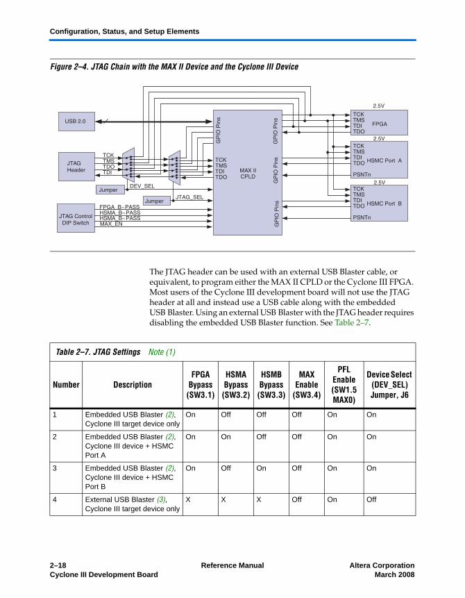
The JTAG chain is mastered by the embedded USB Blaster function found in the MAX II device. Only a USB cable is needed to program the Cyclone III FPGA. Any device can be bypassed by using the appropriate switch on the JTAG control DIP switch.
1 Board reference SW1 position 5 (SW1.5), labeled MAX0, must be in the closed position (on) for this feature to properly work. If the SW1 switch is in the closed position, the PFL megafunction in the MAX II CPLD may try to overwrite the FPGA image just downloaded over the USB immediately after completion.
For more information on:
■ Advanced JTAG settings, refer to Table 2–7. ■ The JTAG control switch, refer to “JTAG Control DIP Switch” on
page 2–22.
Altera Corporation Reference Manual 2–17March 2008 Cyclone III Development Board
Configuration, Status, and Setup Elements
Figure 2–4. JTAG Chain with the MAX II Device and the Cyclone III Device
The JTAG header can be used with an external USB Blaster cable, or equivalent, to program either the MAX II CPLD or the Cyclone III FPGA. Most users of the Cyclone III development board will not use the JTAG header at all and instead use a USB cable along with the embedded USB Blaster. Using an external USB Blaster with the JTAG header requires disabling the embedded USB Blaster function. See Table 2–7.
Table 2–7. JTAG Settings Note (1)
Number DescriptionFPGA
Bypass (SW3.1)
HSMA Bypass (SW3.2)
HSMB Bypass (SW3.3)
MAX Enable
(SW3.4)
PFL Enable (SW1.5 MAX0)
Device Select (DEV_SEL) Jumper, J6
1 Embedded USB Blaster (2), Cyclone III target device only
On Off Off Off On On
2 Embedded USB Blaster (2), Cyclone III device + HSMC Port A
On On Off Off On On
3 Embedded USB Blaster (2), Cyclone III device + HSMC Port B
On Off On Off On On
4 External USB Blaster (3), Cyclone III target device only
X X X Off On Off
2–18 Reference Manual Altera CorporationCyclone III Development Board March 2008
Board Components
FPGA Programming from Flash Memory
On either power-up or by pressing the RESET_CONFIG or FACTORY_CONFIG push button, the MAX II CPLD device’s PFL megafunction will configure the Cyclone III FPGA from flash memory.
The PFL megafunction reads 16-bit data from the flash memory and converts it to passive serial format. The data is written to the Cyclone III device’s dedicated DCLK and D0 configuration pins at 12 MHz.
FPGA configuration from flash memory can be sourced from one of eight images. The image is selected by the PGM_CONFIG_SELECT rotary switch, board reference SW5. The rotary switch has 16 positions, but only the first eight are used. The positions correspond to an offset in flash memory that the PFL is directed to for FPGA configuration data.
1 Board reference SW1 position 5 (SW1.5), labeled MAX0, must be in the open position (off) for this feature to be enabled. If the SW1 switch is in the open position, the PFL megafunction in the MAX II CPLD is disabled.
Flash Programming over USB Interface
The flash memory can be programmed at any time the board is powered up using the USB 2.0 interface and the Quartus II Programmer’s JTAG mode.
The development kit implements the Altera parallel flash loader (PFL) megafunction for flash programming. The PFL is a block of logic that is programmed into an Altera programmable logic device (FPGA or CPLD). The PFL functions as a utility for writing to a compatible flash device. The development kit ships with a pre-built PFL design called
5 External USB Blaster (3), MAX II target device only
X X X X X On
Note to Table 2–7:(1) The nomenclature SW3.1 is used to indicate board reference SW3, position 1; similarly SW1.5 is used to indicate
board reference SW1, position 5. (2) Requires USB cable plugged into board reference J3. (3) Requires external USB Blaster or equivalent plugged into board reference J14 (PCB bottom).
Table 2–7. JTAG Settings Note (1)
Number DescriptionFPGA
Bypass (SW3.1)
HSMA Bypass (SW3.2)
HSMB Bypass (SW3.3)
MAX Enable
(SW3.4)
PFL Enable (SW1.5 MAX0)
Device Select (DEV_SEL) Jumper, J6
Altera Corporation Reference Manual 2–19March 2008 Cyclone III Development Board
Configuration, Status, and Setup Elements
cycloneIII_3c120_dev_pfl. The PFL design is programmed onto the FPGA whenever the flash is to be written using the Quartus II software.
f For more information on:
■ The PFL megafunction, refer to Application Note 386: Using the Parallel Flash Loader with the Quartus II software.
■ Basic flash programming instructions for the development board, refer to the Cyclone III Development User Guide, Appendix A, Programming the Flash Device.
Status Elements
The development board includes general user, board specific, and HSMC user LEDs. This section discusses board-specific LEDs as well as the power display device.
f For information on general and HSMC user-defined LEDS, refer to “User-Defined LEDs” on page 2–33.
Board Specific LEDs
There are 14 board-specific LEDs, which are factory designated. Table 2–8 lists the LED board references, names, and descriptions.
Table 2–8. Board-Specific LEDs (Part 1 of 2)
Board Reference LED Name Description
D5 Power Illuminates when board power switch SW2 is on.(Requires 14 V to 20 V input to DC input jack J2)
D25 CONF DONE Illuminates when FPGA is successfully configured. Driven by Cyclone III FPGA.
D20 Loading Illuminates when MAX II CPLD is actively configuring the FPGA. Driven by the MAX II CPLD.
D21 Error Illuminates when MAX II CPLD fails to successfully configure the FPGA. Driven by the MAX II CPLD.
D24 Factory Illuminates when FPGA is configured with the default factory FPGA design. Driven by the MAX II CPLD.
D22 User Illuminates when FPGA is configured with a design other than the default factory FPGA design. Driven by the MAX II CPLD.
D7 ENET TX Illuminates when transmit data is active from the Ethernet PHY. Driven by the Marvell 88E1111 PHY.
D8 ENET RX Illuminates when receive data is active from the Ethernet PHY. Driven by the Marvell 88E1111 PHY.
2–20 Reference Manual Altera CorporationCyclone III Development Board March 2008
Board Components
Table 2–9 lists the board-specific LEDs component reference and manufacturing information.
Power Display (U28)
The power being measured by the MAX II CPLD and associated A/D is displayed on a dedicated 7-segment display connected to the MAX II device called Power Display. Although the 7-segment display is connected to the MAX II CPLD, it is also register-controllable from the FPGA using the FSM bus.
D1 10 Mb Illuminates when Ethernet PHY is using the 10 Mbps connection speed. Driven by the Marvell 88E1111 PHY.
D3 100 Mb Illuminates when Ethernet PHY is using the 100 Mbps connection speed. Driven by the Marvell 88E1111 PHY.
D4 1000 Mb Illuminates when Ethernet PHY is using the 1000 Mbps connection speed. Driven by the Marvell 88E1111 PHY. Also connects to Cyclone III FPGA.
D6 Duplex Illuminates when Ethernet PHY is both sending and receiving data. Driven by the Marvell 88E1111 PHY.
D18 HSMC Port Apresent
Illuminates when HSMC Port A has a board or cable plugged such that pin 160 becomes grounded.
D19 HSMC Port Bpresent
Illuminates when HSMC Port B has a board or cable plugged such that pin 160 becomes grounded.
D17 SRAM active Illuminates when SRAM is being accessed with a read or write transaction. Driven by the MAX II CPLD.
D23 Flash active Illuminates when flash memory is being accessed with a read or write transaction. Driven by the MAX II CPLD.
Table 2–8. Board-Specific LEDs (Part 2 of 2)
Board Reference LED Name Description
Table 2–9. Board-Specific LEDs Component Reference and Manufacturing Information
Board Reference Description Manufacturer ManufacturingPart Number
Manufacturer Web Site
D1, D3, D4, D6-D8, D17-D19, D20, D22-D25
Green LED, 1206, SMT, clear lens, 2.1 V
Lumex, Inc SML-LX1206GC-TR www.lumex.com
D5 Blue LED, 1206, SMT, clear lens, 3.5 V
Lumex, Inc SML-LX1206USBC-TR www.lumex.com
D21 Red LED, 1206, SMT, clear lens, 2.0 V
Lumex, Inc SML-LX1206IC-TR www.lumex.com
Altera Corporation Reference Manual 2–21March 2008 Cyclone III Development Board
Configuration, Status, and Setup Elements
Setup Elements
The development board includes user, JTAG control, and board-specific DIP switches. The board also includes system reset and configuration push button switches as well as a rotary switches. This section discusses:
■ JTAG control DIP switch■ MAX II device control DIP switch■ System reset and configuration push buttons■ POWER SELECT rotary switch■ PGM CONFIG SELECT rotary switch■ Speaker header
JTAG Control DIP Switch
Board reference SW3 is a 4-position JTAG control DIP switch, and it is provided to either remove or include devices in the active JTAG chain. Additionally, JTAG control DIP switch is also used to disable the embedded USB Blaster cable when using an external USB Blaster cable. See Table 2–10.
Because the JTAG chain also contains the two HSMC interface connectors, the SW3 DIP switch allows data to bypass the HSMC interfaces as well as the MAX II CPLD. See “FPGA Programming Over USB” on page 2–17.
f For information on user-defined DIP switches, refer to “User-Defined DIP Switches” on page 2–32.
Table 2–10. JTAG Control DIP Switch Signal Names & Descriptions
DIP Switch Signal Name Description
1 FPGA_BYPASS 1 = FPGA in JTAG chain0 = FPGA not in JTAG chain
2 HSMA_BYPASS 1 = HSMC Port A in JTAG chain (only if installed)0 = HSMC Port A not in JTAG chain
3 HSMB_BYPASS 1 = HSMC Port B in JTAG chain (only if installed)0 = HSMC Port B not in JTAG chain
4 MAX_EN 1 = MAX II device disabled0 = MAX II device enabled
2–22 Reference Manual Altera CorporationCyclone III Development Board March 2008
Board Components
Table 2–11 lists the JTAG control switch component reference and manufacturing information.
MAX II Device Control DIP Switch
Board reference SW1 is the board settings DIP switch, which controls various features specific to the Cyclone III development board and factory default (board test system) FPGA design: On = logic 0 and off = logic 1.
Table 2–12 lists the switch positions, names, and descriptions.
Table 2–11. JTAG Control Switch Component Reference and Manufacturing Information
Board Reference Description Manufacturer ManufacturingPart Number
SW3 Four-position slider DIP switch C&K Components ITT industries
TDA04H0SB1
Table 2–12. MAX II Device Control DIP Switch Positions, Names, and Descriptions
Switch Name Description
8 MAX_DIP3 Reserved
7 MAX_DIP2 Reserved
6 MAX_DIP1 Reserved
5 MAX_DIP0 1 = MAX II device PFL enabled, 0 = MAX II device PFL disabled
4 MAX_RESERVE1 Reserved
3 MAX_RESERVE0 Reserved
2 VOLTS_WATTS 1 = power display shows mW/mA, 0 = power display shows voltage
1 MWATTS_MAMPS 1 = power display shows mA, 0 = power display shows mW
Altera Corporation Reference Manual 2–23March 2008 Cyclone III Development Board
Configuration, Status, and Setup Elements
Table 2–13 lists the MAX II device control DIP switch component reference and manufacturing information.
System Reset & Configuration Switches
Board reference S6 is the system reset push button switch, RESET_CONFIGn, which is an input to the MAX II device. It forces a reconfiguration of the FPGA from flash memory. The location in flash memory is based on the input from the board settings rotary switch position for the signals PGM [2:0]. The MAX II device uses the RESET_CONFIGn pin as its reset along with the CPU_RESETn pin push button.
Board reference S5 is the CPU reset push button switch, CPU_RESET, which is an input to both the Cyclone III FPGA and the MAX II CPLD. The CPU_RESET push button is intended to be the master reset signal for the FPGA design loaded in the Cyclone III device, and connects to the special function pin called DEV_CLR on the FPGA but is also a regular I/O pin. The MAX II device uses this as its reset along with the RESET_CONFIG and FACTORY_CONFIG push button.
Board reference S7 is the factory push button switch (FACTORY_CONFIG), which is an input to the MAX II device. The FACTORY_CONFIG pin forces a reconfiguration of the FPGA with the factory default FPGA design, which is located at the base of flash memory. See Table 2–14.
Table 2–13. MAX II Device Control DIP Switch Component Reference and Manufacturing Information
Board Reference Description Manufacturer Manufacturing
Part NumberManufacturer
Web Site
SW1 8-position rocker DIP switch Grayhill 76SB08ST www.grayhill.com
Table 2–14. Push Button Switch Signal Names and Functions
Board Reference Description I/O
StandardSchematic
Signal Name
Cyclone III Device
Pin Number
MAX II Device
Pin Number
S7 User defined push button 1.8 V FACTORY_CONFIG — A10
S6 User defined push button 1.8 V RESET_CONFIGn — R16
S5 User defined push button 1.8 V CPU_RESET T21 M9
2–24 Reference Manual Altera CorporationCyclone III Development Board March 2008
Board Components
Table 2–15 lists the push-button switch component reference and manufacturing information.
f For information on user-defined push buttons, refer to “User-Defined Push Button Switches” on page 2–31.
POWER SELECT Rotary Switch
A 16-position rotary switch, board reference SW4, is used to select the current power rail whose power is being measured and displayed on the power display. The rotary switch is connected to the MAX II CPLD, but it also registers readable by the FPGA using the FSM shared bus (flash, SRAM, and MAX II device). Table 2–16 lists the power select rotary switch number, name, power pin, and description.
Table 2–15. Push-Button Switch Component Reference and Manufacturing Information
Board Reference Description Manufacturer Manufacturing
Part NumberManufacturer
Web Site
S5-S7 Push button switch Panasonic EVQAPAC07K www.panasonic.com
Table 2–16. Power Select Rotary Switch Numbers, Names, Pins, and Descriptions (Part 1 of 2)
Number SchematicSignal Name Power Pin Name Description
0 1.2V_INT VCCINT FPGA core power
1 1.2V_VCCD VCCD_PLL FPGA PLL digital power
2 2.5V_VCCA VCCA FPGA PLL analog power
3 1.8V_IO_B7_B8 VCCIO7, VCCIO8 FPGA I/O power banks 7,8
4 1.8V_IO_B3_B4 VCCIO3, VCCIO4 FPGA I/O power banks 3,4
5 2.5V_IO_B1_B2 VCCIO1, VCCIO2 FPGA I/O power banks 1,2
6 2.5V_IO_B5_B6 VCCIO5, VCCIO6 FPGA I/O power banks 5,6
7 1.2V — All non-FPGA 1.2 V power(Ethernet)
8 1.8V — All non-FPGA 1.8 V power(SRAM, Flash, MAX II, and DDR2 devices)
9 2.5V — All non-FPGA 2.5 V power(Ethernet, LEDs, LCD)
A 3.3V — All 3.3 V power (voltage only), Note (1)
B 5.0V — All 5.0 V power (voltage only), Note (1)
C 12V — All 12 V power (voltage only), Note (1)
Altera Corporation Reference Manual 2–25March 2008 Cyclone III Development Board
Configuration, Status, and Setup Elements
Table 2–17 lists power select rotary switch component reference and manufacturing information.
PGM CONFIG SELECT Rotary Switch
A 16-position rotary switch, board reference SW5, is used to select the location in flash memory to load the Cyclone III FPGA design. The rotary switch has 16 positions but only the first eight are used. For information on the flash memory locations, refer to Table 2–58 on page 2–75.
Table 2–18 lists PGM configuration select rotary switch component reference and manufacturing information.
Speaker Header (J5)
A four-pin 0.1” pitch header is used for a PC speaker connection. The FPGA drives an R/C filter from a 2.5 V CMOS I/O pin allowing tones to be generated by driving different frequencies to the pin.
D — — —
E — — —
F — — —
Note to Table 2–16:(1) Display shows resistor divider output, not actual voltage. As the A/D cannot take in sources higher than 3.0 V. See
schematic page 5 for resistor dividers. Current (mA) displays for these voltages are only accurate to see a change in current from one circuit state to another. The absolute current levels should not be referenced.
Table 2–16. Power Select Rotary Switch Numbers, Names, Pins, and Descriptions (Part 2 of 2)
Number SchematicSignal Name Power Pin Name Description
Table 2–17. Power Select Rotary Switch Component Reference and Manufacturing Information
Board Reference Description Manufacturer Manufacturing
Part NumberManufacturer
Web Site
SW4 16-position rotary switch Grayhill Corporation 94HCB16WT www.grayhill.com
Table 2–18. PGM CONFIG SELECT Rotary Switch Component Reference and Manufacturing Information
Board Reference Description Manufacturer Manufacturing
Part NumberManufacturer
Web Site
SW5 Rotary switch Grayhill Corporation 94HCB16WT www.grayhill.com
2–26 Reference Manual Altera CorporationCyclone III Development Board March 2008
Board Components
Table 2–19 lists power select rotary switch component reference and manufacturing information.
Clocking Circuitry
This section describes Cyclone III FPGA clocking inputs and outputs. A diagram is provided for each section.
Cyclone III FPGA Clock Inputs
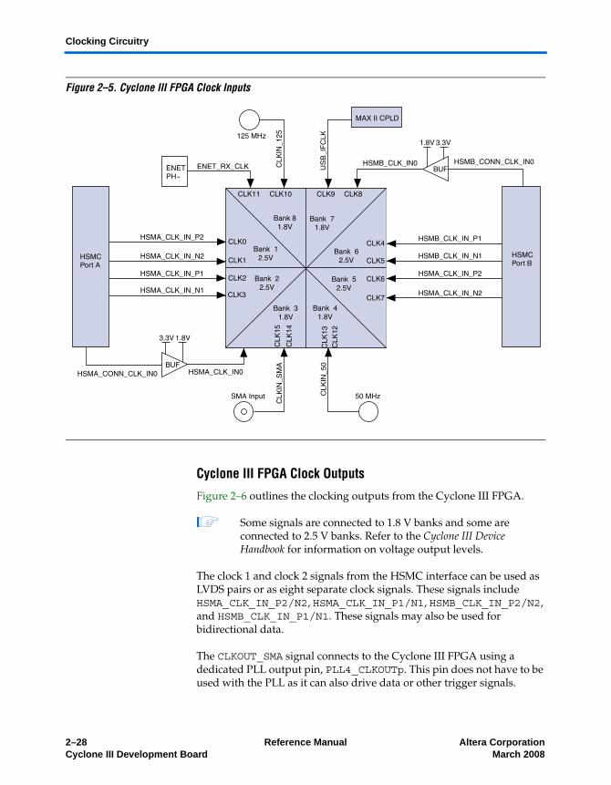
Figure 2–5 outlines the clocking inputs to the Cyclone III FPGA.
1 Some signals are connected to 1.8 V banks and some are connected to 2.5 V banks. Refer to the Cyclone III Device Handbook for information on allowable levels for driving these inputs from external sources.
The clock 1 and clock 2 signals from the HSMC interface can be used as LVDS pairs or as eight separate clock signals. These signals include HSMA_CLK_IN_P2/N2, HSMA_CLK_IN_P1/N1, HSMB_CLK_IN_P2/N2, and HSMB_CLK_IN_P1/N1. These signals may also be used for bidirectional data. If used in LVDS mode, install applicable termination resistors between P/N pairs. A voltage translator, National Semiconductor part number FXLP34, is located in between the HSMC interfaces and the Cyclone III FPGA to reduce LVTTL to 1.8 V CMOS input levels for clock 0 signals HSMA_CLK_IN0 and HSMB_CLK_IN0.
f For more information, refer to the Cyclone III development board schematics included with the Cyclone III Development Board Kit.
Table 2–19. Power Select Rotary Switch Component Reference and Manufacturing Information
Board Reference Description Manufacturer Manufacturing
Part NumberManufacturer
Web Site
J5 Speaker header Samtec TSW-104-07-G-S www.samtec.com
Altera Corporation Reference Manual 2–27March 2008 Cyclone III Development Board
Clocking Circuitry
Figure 2–5. Cyclone III FPGA Clock Inputs
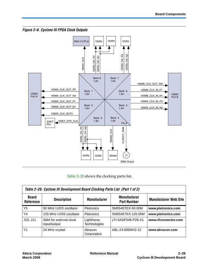
Cyclone III FPGA Clock Outputs
Figure 2–6 outlines the clocking outputs from the Cyclone III FPGA.
1 Some signals are connected to 1.8 V banks and some are connected to 2.5 V banks. Refer to the Cyclone III Device Handbook for information on voltage output levels.
The clock 1 and clock 2 signals from the HSMC interface can be used as LVDS pairs or as eight separate clock signals. These signals include HSMA_CLK_IN_P2/N2, HSMA_CLK_IN_P1/N1, HSMB_CLK_IN_P2/N2, and HSMB_CLK_IN_P1/N1. These signals may also be used for bidirectional data.
The CLKOUT_SMA signal connects to the Cyclone III FPGA using a dedicated PLL output pin, PLL4_CLKOUTp. This pin does not have to be used with the PLL as it can also drive data or other trigger signals.
2–28 Reference Manual Altera CorporationCyclone III Development Board March 2008
Board Components
Figure 2–6. Cyclone III FPGA Clock Outputs
Table 2–20 shows the clocking parts list.
Table 2–20. Cyclone III Development Board Clocking Parts List (Part 1 of 2)
Board Reference Description Manufacturer Manufacturer
Part Number Manufacturer Web Site
Y5 50 MHz LVDS oscillator Pletronics SM5545TEX-50.00M www.pletronics.com
Y4 125 MHz LVDS oscillator Pletronics SM5545TEX-125.00M www.pletronics.com
J10, J11 SMA for external clock input/output
Lighthorse Technologies
LTI-SASF546-P26-X1 www.rfconnector.com
Y1 24 MHz crystal Abracon Corporation
ABL-24.000MHZ-12 www.abracon.com
Altera Corporation Reference Manual 2–29March 2008 Cyclone III Development Board
Clocking Circuitry
Table 2–21 lists the board’s clock distribution system.
Oscillators
There are several on-board crystals and crystal oscillators driving reference clocks to different devices. See Table 2–22.
Y2 6 MHz crystal Abracon Corporation
ABL-6.000MHZ-B2 www.abracon.com
X1 25 MHz crystal oscillator ECS, Inc. ECS-3953C-250-B www.ecsxtal.com
Y3 24 MHz crystal oscillator Pletronics SM5545TEX-24.00M www.pletronics.com
Table 2–20. Cyclone III Development Board Clocking Parts List (Part 2 of 2)
Board Reference Description Manufacturer Manufacturer
Part Number Manufacturer Web Site
Table 2–21. Cyclone III Development Board Clock Distribution
Source SchematicSignal Name I/O Standard
Signal Originates
FromSignal Propagates To
125 MHz (Y4) oscillator clkin_125 Input Y4 Cyclone III device pin A14
50 MHz (Y5) oscillator clkin_50 Input Y5 Cyclone III device pin E13
User input (SMA clock input)
clkin_sma Input J10 Cyclone III device pin AH14
User output (SMA clock output)
clkout_sma Output J11 From Cyclone III device pin AE23
25 MHz (reference clock) This clock can change both speed and direction depending on the Ethernet link speed (10/100/1000)
enet_rx_clk Input U5 Cyclone III device pin B14
24 MHz (Y3) oscillator clkin_24 Input Y3 MAX II device pin J12 (Bank 3)
6 MHz crystal XTIN/XTOUT Input Y2 FTDI USB PHY
24 MHz crystal XTALIN/XTALOUT Input Y1 Cypress USB PHY
Table 2–22. Board Oscillators (Part 1 of 2)
Number Frequency Description
1 6.000 MHz Crystal for FTDI USB PHY
2 24.000 MHz Crystal for Cypress USB PHY
2–30 Reference Manual Altera CorporationCyclone III Development Board March 2008
Board Components
General User Interfaces
To allow you to fully leverage the I/O capabilities of the Cyclone III device for debugging, control, and monitoring purposes, the following general user interfaces are available on the board:
■ Push buttons■ DIP switches■ LEDs■ 7-segment displays■ LCD displays
User-Defined Push Button Switches
The development board includes four general user, one user reset, one system reset, and one factory push button switch. For information on the system reset and factory push button switches, refer to “System Reset & Configuration Switches” on page 2–24.
Board references S1 through S4 are push button switches allowing general user I/O interfaces to the Cyclone III device. There is no board-specific function for these four push buttons.
Board reference S5 is the user reset push button switch, CPU_RESETn, which is an input to the Cyclone III device and MAX II CPLD. It is intended to be the master reset signal for the FPGA design loaded into the Cyclone III device. This connects to the special function pin called the DEV_CLR on the FPGA, but it also is a regular I/O pin. The MAX II device uses the DEV_CLR pin as its reset along with the RESET_CONFIGn push button.
3 24.000 MHz Crystal oscillator for MAX II CPLD
4 25.000 MHz Crystal oscillator for Ethernet PHY
5 50.000 MHz Crystal oscillator for Cyclone III FPGA PLL
6 125.000 MHz Crystal oscillator for Cyclone III FPGA PLL
Table 2–22. Board Oscillators (Part 2 of 2)
Number Frequency Description
Altera Corporation Reference Manual 2–31March 2008 Cyclone III Development Board
General User Interfaces
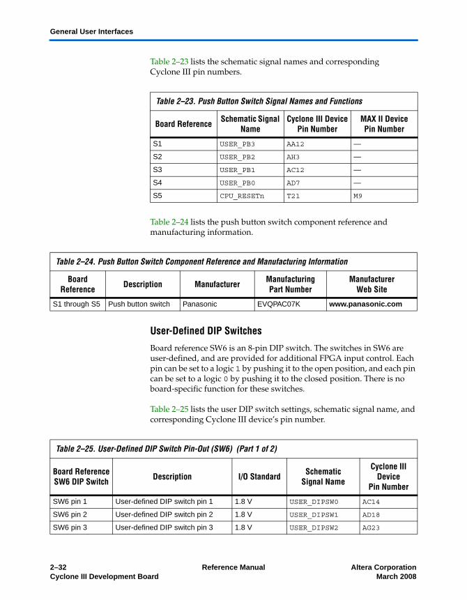
Table 2–23 lists the schematic signal names and corresponding Cyclone III pin numbers.
Table 2–24 lists the push button switch component reference and manufacturing information.
User-Defined DIP Switches
Board reference SW6 is an 8-pin DIP switch. The switches in SW6 are user-defined, and are provided for additional FPGA input control. Each pin can be set to a logic 1 by pushing it to the open position, and each pin can be set to a logic 0 by pushing it to the closed position. There is no board-specific function for these switches.
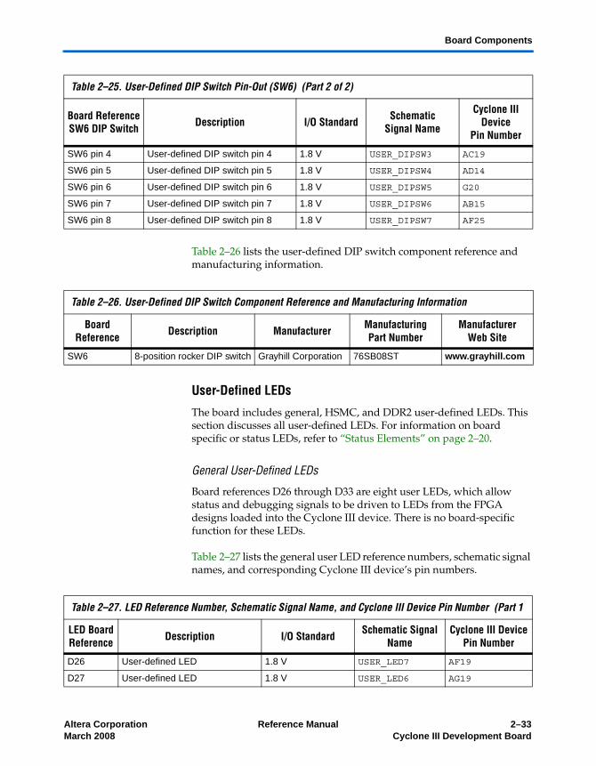
Table 2–25 lists the user DIP switch settings, schematic signal name, and corresponding Cyclone III device’s pin number.
Table 2–23. Push Button Switch Signal Names and Functions
Board Reference Schematic Signal Name
Cyclone III DevicePin Number
MAX II DevicePin Number
S1 USER_PB3 AA12 —
S2 USER_PB2 AH3 —
S3 USER_PB1 AC12 —
S4 USER_PB0 AD7 —
S5 CPU_RESETn T21 M9
Table 2–24. Push Button Switch Component Reference and Manufacturing Information
Board Reference Description Manufacturer Manufacturing
Part NumberManufacturer
Web Site
S1 through S5 Push button switch Panasonic EVQPAC07K www.panasonic.com
Table 2–25. User-Defined DIP Switch Pin-Out (SW6) (Part 1 of 2)
Board ReferenceSW6 DIP Switch Description I/O Standard Schematic
Signal Name
Cyclone III Device
Pin Number
SW6 pin 1 User-defined DIP switch pin 1 1.8 V USER_DIPSW0 AC14
SW6 pin 2 User-defined DIP switch pin 2 1.8 V USER_DIPSW1 AD18
SW6 pin 3 User-defined DIP switch pin 3 1.8 V USER_DIPSW2 AG23
2–32 Reference Manual Altera CorporationCyclone III Development Board March 2008
Board Components
Table 2–26 lists the user-defined DIP switch component reference and manufacturing information.
User-Defined LEDs
The board includes general, HSMC, and DDR2 user-defined LEDs. This section discusses all user-defined LEDs. For information on board specific or status LEDs, refer to “Status Elements” on page 2–20.
General User-Defined LEDs
Board references D26 through D33 are eight user LEDs, which allow status and debugging signals to be driven to LEDs from the FPGA designs loaded into the Cyclone III device. There is no board-specific function for these LEDs.
Table 2–27 lists the general user LED reference numbers, schematic signal names, and corresponding Cyclone III device’s pin numbers.
SW6 pin 4 User-defined DIP switch pin 4 1.8 V USER_DIPSW3 AC19
SW6 pin 5 User-defined DIP switch pin 5 1.8 V USER_DIPSW4 AD14
SW6 pin 6 User-defined DIP switch pin 6 1.8 V USER_DIPSW5 G20
SW6 pin 7 User-defined DIP switch pin 7 1.8 V USER_DIPSW6 AB15
SW6 pin 8 User-defined DIP switch pin 8 1.8 V USER_DIPSW7 AF25
Table 2–25. User-Defined DIP Switch Pin-Out (SW6) (Part 2 of 2)
Board ReferenceSW6 DIP Switch Description I/O Standard Schematic
Signal Name
Cyclone III Device
Pin Number
Table 2–26. User-Defined DIP Switch Component Reference and Manufacturing Information
Board Reference Description Manufacturer Manufacturing
Part NumberManufacturer
Web Site
SW6 8-position rocker DIP switch Grayhill Corporation 76SB08ST www.grayhill.com
Table 2–27. LED Reference Number, Schematic Signal Name, and Cyclone III Device Pin Number (Part 1
LED BoardReference Description I/O Standard Schematic Signal
NameCyclone III Device
Pin Number
D26 User-defined LED 1.8 V USER_LED7 AF19
D27 User-defined LED 1.8 V USER_LED6 AG19
Altera Corporation Reference Manual 2–33March 2008 Cyclone III Development Board
General User Interfaces
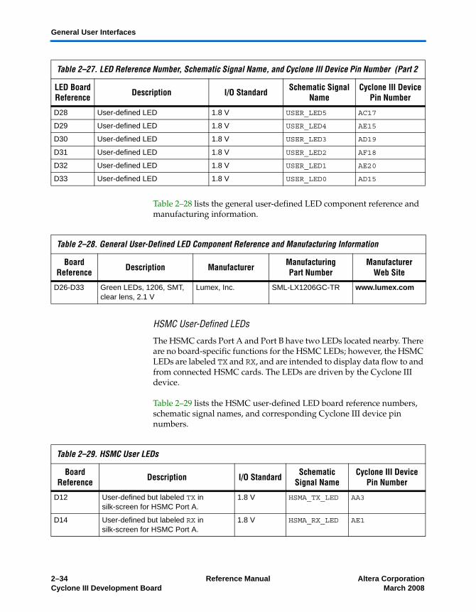
Table 2–28 lists the general user-defined LED component reference and manufacturing information.
HSMC User-Defined LEDs
The HSMC cards Port A and Port B have two LEDs located nearby. There are no board-specific functions for the HSMC LEDs; however, the HSMC LEDs are labeled TX and RX, and are intended to display data flow to and from connected HSMC cards. The LEDs are driven by the Cyclone III device.
Table 2–29 lists the HSMC user-defined LED board reference numbers, schematic signal names, and corresponding Cyclone III device pin numbers.
D28 User-defined LED 1.8 V USER_LED5 AC17
D29 User-defined LED 1.8 V USER_LED4 AE15
D30 User-defined LED 1.8 V USER_LED3 AD19
D31 User-defined LED 1.8 V USER_LED2 AF18
D32 User-defined LED 1.8 V USER_LED1 AE20
D33 User-defined LED 1.8 V USER_LED0 AD15
Table 2–27. LED Reference Number, Schematic Signal Name, and Cyclone III Device Pin Number (Part 2
LED BoardReference Description I/O Standard Schematic Signal
NameCyclone III Device
Pin Number
Table 2–28. General User-Defined LED Component Reference and Manufacturing Information
Board Reference Description Manufacturer Manufacturing
Part NumberManufacturer
Web Site
D26-D33 Green LEDs, 1206, SMT, clear lens, 2.1 V
Lumex, Inc. SML-LX1206GC-TR www.lumex.com
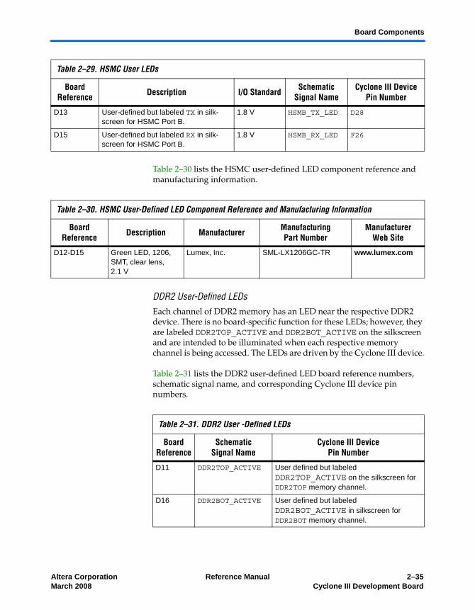
Table 2–29. HSMC User LEDs
Board Reference Description I/O Standard Schematic
Signal NameCyclone III Device
Pin Number
D12 User-defined but labeled TX in silk-screen for HSMC Port A.
1.8 V HSMA_TX_LED AA3
D14 User-defined but labeled RX in silk-screen for HSMC Port A.
1.8 V HSMA_RX_LED AE1
2–34 Reference Manual Altera CorporationCyclone III Development Board March 2008
Board Components
Table 2–30 lists the HSMC user-defined LED component reference and manufacturing information.
DDR2 User-Defined LEDsEach channel of DDR2 memory has an LED near the respective DDR2 device. There is no board-specific function for these LEDs; however, they are labeled DDR2TOP_ACTIVE and DDR2BOT_ACTIVE on the silkscreen and are intended to be illuminated when each respective memory channel is being accessed. The LEDs are driven by the Cyclone III device.
Table 2–31 lists the DDR2 user-defined LED board reference numbers, schematic signal name, and corresponding Cyclone III device pin numbers.
D13 User-defined but labeled TX in silk-screen for HSMC Port B.
1.8 V HSMB_TX_LED D28
D15 User-defined but labeled RX in silk-screen for HSMC Port B.
1.8 V HSMB_RX_LED F26
Table 2–29. HSMC User LEDs
Board Reference Description I/O Standard Schematic
Signal NameCyclone III Device
Pin Number
Table 2–30. HSMC User-Defined LED Component Reference and Manufacturing Information
Board Reference Description Manufacturer Manufacturing
Part NumberManufacturer
Web Site
D12-D15 Green LED, 1206, SMT, clear lens, 2.1 V
Lumex, Inc. SML-LX1206GC-TR www.lumex.com
Table 2–31. DDR2 User -Defined LEDs
Board Reference
SchematicSignal Name
Cyclone III DevicePin Number
D11 DDR2TOP_ACTIVE User defined but labeled DDR2TOP_ACTIVE on the silkscreen for DDR2TOP memory channel.
D16 DDR2BOT_ACTIVE User defined but labeled DDR2BOT_ACTIVE in silkscreen for DDR2BOT memory channel.
Altera Corporation Reference Manual 2–35March 2008 Cyclone III Development Board
General User Interfaces
Table 2–32 lists the memory user-defined LED component reference and manufacturing information.
7-Segment Displays
This section discusses the following two on-board displays:
■ User 7-segment display■ Power 7-segment display
User 7-Segment Display
Board reference U30 is a four-digit, user-defined, 7-segment display that is labeled User Display. Each segment’s LED driver input signals are multiplexed to each of the four digits and a minus sign. A small HDL code snippet continuously writes to each of the four segments so that they appear constantly illuminated.
Table 2–33 lists the 7-segment display pin-out.
Table 2–32. Memory User-Defined LED Component Reference and Manufacturing Information
Board Reference Description Manufacturer Manufacturing
Part NumberManufacturer
Web Site
D11 and D16 Green LED, 1206, SMT, clear lens 2.1 V
Lumex, Inc. SML-LX1206GC-TR www.lumex.com
Table 2–33. 7-Segment Display Pin-Out (Part 1 of 2)
BoardReference Description I/O
StandardSchematic
Signal Name
Cyclone III Device
Pin Name
U30 pin 12 User-defined display signal 1.8 V SEVEN_SEG_A AD5
U30 pin 11 User-defined display signal 1.8 V SEVEN_SEG_B A3
U30 pin 3 User-defined display signal 1.8 V SEVEN_SEG_C C4
U30 pin 8 User-defined display signal 1.8 V SEVEN_SEG_D D4
U30 pin 9 User-defined display signal 1.8 V SEVEN_SEG_E E5
U30 pin 7 User-defined display signal 1.8 V SEVEN_SEG_F D5
U30 pin 5 User-defined display signal 1.8 V SEVEN_SEG_G AE6
U30 pin 2 User-defined display signal 1.8 V SEVEN_SEG_DP AD4
U30 pin 13 User-defined display signal 1.8 V SEVEN_SEG_SEL1 B3
U30 pin 1 User-defined display select signal 1.8 V SEVEN_SEG_SEL2 C5
2–36 Reference Manual Altera CorporationCyclone III Development Board March 2008
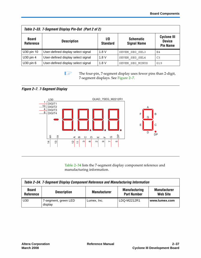
Board Components
1 The four-pin, 7-segment display uses fewer pins than 2-digit, 7-segment displays. See Figure 2–7.
Figure 2–7. 7-Segment Display
Table 2–34 lists the 7-segment display component reference and manufacturing information.
U30 pin 10 User-defined display select signal 1.8 V SEVEN_SEG_SEL3 E4
U30 pin 4 User-defined display select signal 1.8 V SEVEN_SEG_SEL4 C3
U30 pin 6 User-defined display select signal 1.8 V SEVEN_SEG_MINUS G19
Table 2–33. 7-Segment Display Pin-Out (Part 2 of 2)
BoardReference Description I/O
StandardSchematic
Signal Name
Cyclone III Device
Pin Name
Table 2–34. 7-Segment Display Component Reference and Manufacturing Information
Board Reference Description Manufacturer Manufacturing
Part NumberManufacturer
Web Site
U30 7-segment, green LED display
Lumex, Inc. LDQ-M2212R1 www.lumex.com
Altera Corporation Reference Manual 2–37March 2008 Cyclone III Development Board
General User Interfaces
Power 7-Segment Display
The power measured by the MAX II CPLD and associated A/D is displayed on board reference U28, which is a dedicated 7-segment display connected to the MAX II CPLD, labeled Power Display.
Table 2–35 lists the power 7-segment display component reference and manufacturing information.
LCD Displays
The development board is designed to accommodate two separate displays:
■ Character LCD■ Graphics LCD
The first display is a 16-character, by 2-line LCD display. The second is a 128 x 64 pixel transmissive graphics LCD. These two share a common bus but have separate control signals so they can operate simultaneously. This section describes both displays.
Character LCD (J4)
The board contains a single 14-pin 0.1” pitch dual-row header, used to interface to a 16-character by 2-line LCD display, Lumex (part number LCM-S01602DSR/C). The LCD has a 14-pin receptacle that mounts directly to the board’s 14-pin header, so it can be easily removed for access to components under the display—or to use the header for debugging or other purposes.
Table 2–35. Power 7-Segment Display Component Reference and Manufacturing Information
Board Reference Description Manufacturer Manufacturing
Part NumberManufacturer
Web Site
U28 7-segment, green LED display
Lumex, Inc. LDQ-M2212R1 www.lumex.com
2–38 Reference Manual Altera CorporationCyclone III Development Board March 2008
Board Components
Table 2–36 summarizes the character LCD interface pins. Signal names and directions are relative to the Cyclone III FPGA. For functional descriptions, see Table 2–37.
Table 2–37 shows pin definitions, and is an excerpt from the Lumex data sheet.
f For more information such as timing, character maps, interface guidelines, and related documentation, visit www.lumex.com.
Table 2–36. Character LCD Header I/O
BoardReference Description I/O Standard Schematic
Signal NameCyclone III Pin Number
J22 pin 7 LCD data bus bit 0 2.5 V LCD_DATA0 AA4
J22 pin 8 LCD data bus bit 1 2.5 V LCD_DATA1 AD1
J22 pin 9 LCD data bus bit 2 2.5 V LCD_DATA2 V8
J22 pin 10 LCD data bus bit 3 2.5 V LCD_DATA3 AB5
J22 pin 11 LCD data bus bit 4 2.5 V LCD_DATA4 AE2
J22 pin 12 LCD data bus bit 5 2.5 V LCD_DATA5 V5
J22 pin 13 LCD data bus bit 6 2.5 V LCD_DATA6 V6
J22 pin 14 LCD data bus bit 7 2.5 V LCD_DATA7 AB3
J22 pin 4 LCD data/command select 2.5 V LCD_D_Cn D27
J22 pin 5 LCD write enable 2.5 V LCD_D_WEn AC4
J22 pin 6 LCD chip select 2.5 V LCD_D_CSn AB24
Table 2–37. Character LCD Display Pin Definitions
Pin Number Symbol Level Function
1 VDD — Power supply 5 V
2 VSS — GND (0V)
3 V0 — For LCD drive
4 RS H/L Register select signalH: Data inputL: Instruction input
5 R/W H/L H: Data read (module to MPU)L: Data write (MPU to module)
6 E H, H to L Enable
7~14 DB0~DB7 H/L Data bus, software selectable 4 or 8 bit mode
Altera Corporation Reference Manual 2–39March 2008 Cyclone III Development Board
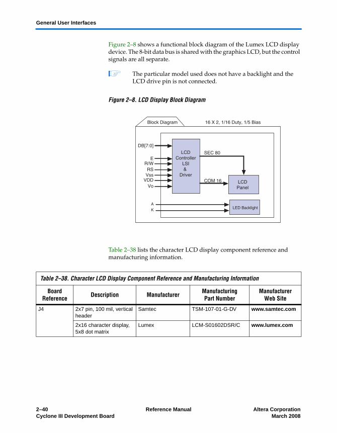
General User Interfaces
Figure 2–8 shows a functional block diagram of the Lumex LCD display device. The 8-bit data bus is shared with the graphics LCD, but the control signals are all separate.
1 The particular model used does not have a backlight and the LCD drive pin is not connected.
Figure 2–8. LCD Display Block Diagram
Table 2–38 lists the character LCD display component reference and manufacturing information.
Table 2–38. Character LCD Display Component Reference and Manufacturing Information
Board Reference Description Manufacturer Manufacturing
Part NumberManufacturer
Web Site
J4 2x7 pin, 100 mil, vertical header
Samtec TSM-107-01-G-DV www.samtec.com
2x16 character display, 5x8 dot matrix
Lumex LCM-S01602DSR/C www.lumex.com
2–40 Reference Manual Altera CorporationCyclone III Development Board March 2008
Board Components
Graphics LCD (J13)
The board contains a 30-pin, fine-pitch connector to interface directly to a 128 X 64 dot matrix graphics LCD display via a flex-cable that is soldered to the display itself. The display is an Optrex part number F-51852GNFQJ-LB-AIN (blue pixels) or F-51852GNFQJ-LB-CAN (green pixels). The pinout of this interface connector is compatible with a variety of displays.
1 The data signals are bussed with the 14-pin LCD header.
f For the graphics LCD data sheet and related documentation, visit www.optrex.com.
Table 2–39 lists the graphics LCD pin names, descriptions, and type. Signal names and directions are relative to the Cyclone III FPGA.
Table 2–39. Graphics LCD Interface I/O
BoardReference Description I/O
StandardSchematic
Signal NameCyclone III Device
Pin Number
J13 pin 6 LCD data bus bit 0 2.5 V LCD_DATA0 AA4
J13 pin 7 LCD data bus bit 1 2.5 V LCD_DATA1 AD1
J13 pin 8 LCD data bus bit 2 2.5 V LCD_DATA2 V8
J13 pin 9 LCD data bus bit 3 2.5 V LCD_DATA3 AB5
J13 pin 10 LCD data bus bit 4 2.5 V LCD_DATA4 AE2
J13 pin 11 LCD data bus bit 5 2.5 V LCD_DATA5 V5
J13 pin 12 LCD data bus bit 6 _or SCLK 2.5 V LCD_DATA6 V6
J13 pin 13 LCD data bus bit 7 _or SDATA 2.5 V LCD_DATA7 AB3
J13 pin 28 Parallel interface selection_high = 68 series, low = 80 series
2.5 V LCD_BS1 Note (1)
J13 pin 1 LCD chip select 2.5 V LCD_CSn AB24
J13 pin 3 LCD data/command select 2.5 V LCD_D_Cn D27
J13 pin 5 LCD read enable 2.5 V LCD_E_RDn V7
J13 pin 2 LCD reset 2.5 V LCD_RSTn H7
J13 pin 29 LCD parallel/serial data select 2.5 V LCD_SERn Note (1)
J13 pin 4 LCD write enable 2.5 V LCD_WEn AC4
Note to Table 2–39:(1) For the corresponding Cyclone III device pin number, refer to MAX II device pinout tables on the MAX II device
literature page, www.altera.com/literature/lit-max2.jsp.<Is this the preferred link?>
Altera Corporation Reference Manual 2–41March 2008 Cyclone III Development Board
General User Interfaces
Table 2–40 is an excerpt from the OPTREX data sheet showing pin definitions for both serial and parallel interfaces. The included display has a parallel interface.
f For more information about the data sheet and related documentation, visit Lumex at www.lumex.com.
Table 2–40. Graphics LCD Pin Definitions (Part 1 of 2)
Pin NumberParallel I/F
Name Description
1 CS1 Chip select signal L: active
2 RES Reset signal L: reset
3 A0 H: D0 to D7 are display data; L: D0 to D7 are instructions
4 WR 80 family CPU: reset signal L: active
5 RD 80 family CPU: reset signal L: active
6 D0 Display data
7 D1 Display data
8 D2 Display data
9 D3 Display data
10 D4 Display data
11 D5 Display data
12 D6 (SCL) Display data (serial data clock signal input)
13 D7 (S1) Display data (serial data input
14 VD0 Power supply for logic
15 VSS Power supply (0V.GND)
16 VOUT DC/DC voltage converter output
17 C3- DC/DC voltage converter negative connection
18 C1+ DC/DC voltage converter positive connection
19 C1- DC/DC voltage converter negative connection
20 C2- DC/DC voltage converter negative connection
21 C2+ DC/DC voltage converter positive connection
22 V1 Power supply for LCD drive V1 = 1/9-VS
23 V2 Power supply for LCD drive V2 = 2/9-VS
2–42 Reference Manual Altera CorporationCyclone III Development Board March 2008
Board Components
1 Board defaults graphics LCD interface to 80 series CPU mode and parallel interface. These defaults can be modified by writing to the appropriate register in the MAX II CPLD using the FSM bus.
Figure 2–9 is an excerpt from the OPTREX data sheet showing the control chip in the LCD module. The control chip is from New Japan Radio Corporation (part number NJU6676), and Figure 2–9 illustrates the functional block diagram of the display driver.
f For more information, contact Optrex American at www.optrex.com or New Japan Radio at www.njr.co.jp/index_e.htm.
24 V3 Power supply for LCD drive V3 = 7/9-VS
25 V4 Power supply for LCD drive V4 = 8/9-VS
26 V5 Power supply for LCD drive V5,VOUT
27 VR Voltage adjustment pin. Applies voltage between VCC and VS using a resistive divider
28 C86 Interface mode select signal H:68 series L: 80 series
29 P/S Parallel/serial data select signal H: parallel L: serial
30 N/C Non-connection
Table 2–40. Graphics LCD Pin Definitions (Part 2 of 2)
Pin NumberParallel I/F
Name Description
Altera Corporation Reference Manual 2–43March 2008 Cyclone III Development Board
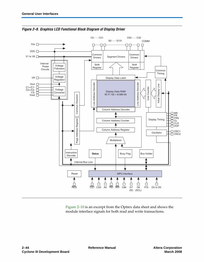
General User Interfaces
Figure 2–9. Graphics LCD Functional Block Diagram of Display Driver
Figure 2–10 is an excerpt from the Optrex data sheet and shows the module interface signals for both read and write transactions.
2–44 Reference Manual Altera CorporationCyclone III Development Board March 2008
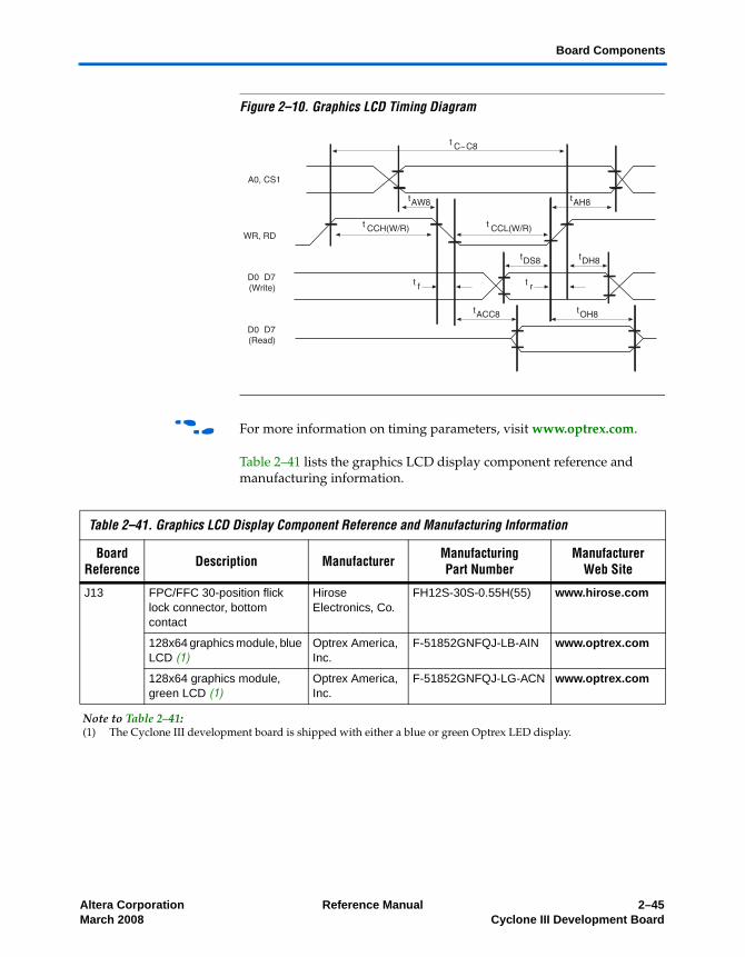
Board Components
Figure 2–10. Graphics LCD Timing Diagram
f For more information on timing parameters, visit www.optrex.com.
Table 2–41 lists the graphics LCD display component reference and manufacturing information.
Table 2–41. Graphics LCD Display Component Reference and Manufacturing Information
Board Reference Description Manufacturer Manufacturing
Part NumberManufacturer
Web Site
J13 FPC/FFC 30-position flick lock connector, bottom contact
Hirose Electronics, Co.
FH12S-30S-0.55H(55) www.hirose.com
128x64 graphics module, blue LCD (1)
Optrex America, Inc.
F-51852GNFQJ-LB-AIN www.optrex.com
128x64 graphics module, green LCD (1)
Optrex America, Inc.
F-51852GNFQJ-LG-ACN www.optrex.com
Note to Table 2–41:(1) The Cyclone III development board is shipped with either a blue or green Optrex LED display.
Altera Corporation Reference Manual 2–45March 2008 Cyclone III Development Board
Communication Ports & Interface Cards
Communication Ports & Interface Cards
This section describes the board’s communication ports and interface cards relative to the Cyclone III device.
The board supports the following communication ports:
■ USB 2.0 MAC/PHY■ 10/100/1000 Ethernet■ High speed Mezzanine cards
USB 2.0 MAC/PHY
The board incorporates the FTDI USB 2.0 PHY chip. The FT245BL (LQFP package) provides an easy cost-effective method of transferring data to/from a peripheral and a host PC at up to 8 million bits (1 Megabyte) per second (Mbps). The simple, FIFO-like design makes interfacing easier.
The device interfaces to J3, a Type B USB connector similar to those used by common peripherals such as digital cameras and printers. The maximum speed of the interface is 12 Mb/s. Typical application speeds are around 1.5 Mb/s; however, actual system speed may vary.
The primary usage for the USB device is to provide JTAG programming of on-board devices such as the FPGA and flash memory. The interface is also the default means through which the FPGA connects to host PC applications such as SignalTap® II, DSP Builder, and the Nios II JTAG universal asynchronous receiver/transmitter (UART).
Figure 2–11 shows the functional block diagram of the FTDI USB PHY device.
2–46 Reference Manual Altera CorporationCyclone III Development Board March 2008
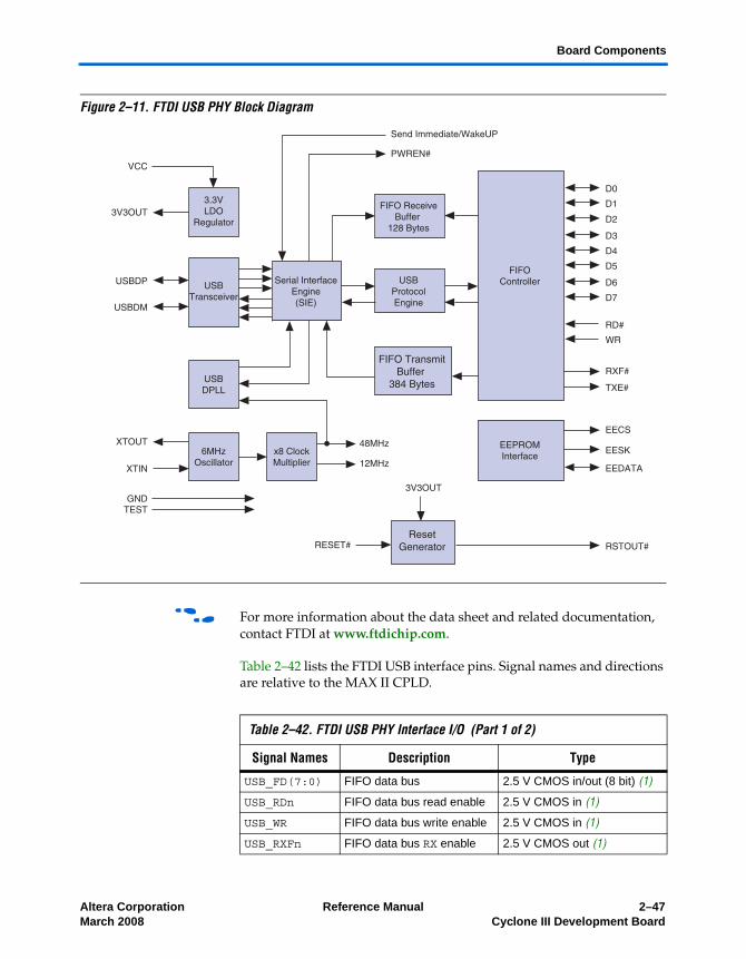
Board Components
Figure 2–11. FTDI USB PHY Block Diagram
f For more information about the data sheet and related documentation, contact FTDI at www.ftdichip.com.
Table 2–42 lists the FTDI USB interface pins. Signal names and directions are relative to the MAX II CPLD.
Table 2–42. FTDI USB PHY Interface I/O (Part 1 of 2)
Signal Names Description Type
USB_FD(7:0) FIFO data bus 2.5 V CMOS in/out (8 bit) (1)
USB_RDn FIFO data bus read enable 2.5 V CMOS in (1)
USB_WR FIFO data bus write enable 2.5 V CMOS in (1)
USB_RXFn FIFO data bus RX enable 2.5 V CMOS out (1)
Altera Corporation Reference Manual 2–47March 2008 Cyclone III Development Board
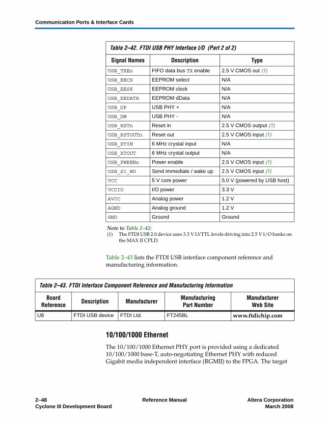
Communication Ports & Interface Cards
Table 2–43 lists the FTDI USB interface component reference and manufacturing information.
10/100/1000 Ethernet
The 10/100/1000 Ethernet PHY port is provided using a dedicated 10/100/1000 base-T, auto-negotiating Ethernet PHY with reduced Gigabit media independent interface (RGMII) to the FPGA. The target
USB_TXEn FIFO data bus TX enable 2.5 V CMOS out (1)
USB_EECS EEPROM select N/A
USB_EESK EEPROM clock N/A
USB_EEDATA EEPROM dData N/A
USB_DP USB PHY + N/A
USB_DM USB PHY - N/A
USB_RSTn Reset in 2.5 V CMOS output (1)
USB_RSTOUTn Reset out 2.5 V CMOS input (1)
USB_XTIN 6 MHz crystal input N/A
USB_XTOUT 6 MHz crystal output N/A
USB_PWRENn Power enable 2.5 V CMOS input (1)
USB_SI_WU Send immediate / wake up 2.5 V CMOS input (1)
VCC 5 V core power 5.0 V (powered by USB host)
VCCIO I/O power 3.3 V
AVCC Analog power 1.2 V
AGND Analog ground 1.2 V
GND Ground Ground
Note to Table 2–42:(1) The FTDI USB 2.0 device uses 3.3 V LVTTL levels driving into 2.5 V I/O banks on
the MAX II CPLD.
Table 2–42. FTDI USB PHY Interface I/O (Part 2 of 2)
Signal Names Description Type
Table 2–43. FTDI Interface Component Reference and Manufacturing Information
Board Reference Description Manufacturer Manufacturing
Part NumberManufacturer
Web Site
U8 FTDI USB device FTDI Ltd. FT245BL www.ftdichip.com
2–48 Reference Manual Altera CorporationCyclone III Development Board March 2008
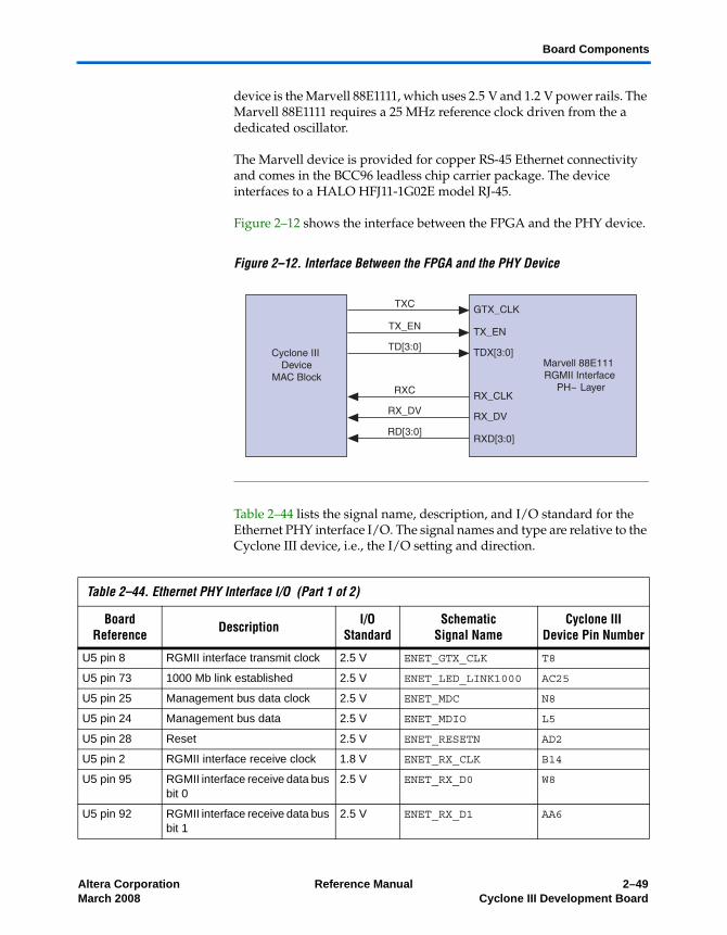
Board Components
device is the Marvell 88E1111, which uses 2.5 V and 1.2 V power rails. The Marvell 88E1111 requires a 25 MHz reference clock driven from the a dedicated oscillator.
The Marvell device is provided for copper RS-45 Ethernet connectivity and comes in the BCC96 leadless chip carrier package. The device interfaces to a HALO HFJ11-1G02E model RJ-45.
Figure 2–12 shows the interface between the FPGA and the PHY device.
Figure 2–12. Interface Between the FPGA and the PHY Device
Table 2–44 lists the signal name, description, and I/O standard for the Ethernet PHY interface I/O. The signal names and type are relative to the Cyclone III device, i.e., the I/O setting and direction.
Table 2–44. Ethernet PHY Interface I/O (Part 1 of 2)
Board Reference Description I/O
StandardSchematic
Signal NameCyclone III
Device Pin Number
U5 pin 8 RGMII interface transmit clock 2.5 V ENET_GTX_CLK T8
U5 pin 73 1000 Mb link established 2.5 V ENET_LED_LINK1000 AC25
U5 pin 25 Management bus data clock 2.5 V ENET_MDC N8
U5 pin 24 Management bus data 2.5 V ENET_MDIO L5
U5 pin 28 Reset 2.5 V ENET_RESETN AD2
U5 pin 2 RGMII interface receive clock 1.8 V ENET_RX_CLK B14
U5 pin 95 RGMII interface receive data bus bit 0
2.5 V ENET_RX_D0 W8
U5 pin 92 RGMII interface receive data bus bit 1
2.5 V ENET_RX_D1 AA6
Altera Corporation Reference Manual 2–49March 2008 Cyclone III Development Board
Communication Ports & Interface Cards
Table 2–45 is an excerpt from the Marvell data sheet with a summary of the RGMII interface signals and their functions.
U5 pin 93 RGMII interface receive data bus bit 2
2.5 V ENET_RX_D2 W7
U5 pin 91 RGMII interface receive data bus bit 3
2.5 V ENET_RX_D3 Y6
U5 pin 94 RGMII interface receive control 2.5 V ENET_RX_DV AB4
U5 pin 11 RGMII interface transmit data bus bit 0
2.5 V ENET_TX_D0 W4
U5 pin 12 RGMII interface transmit data bus bit 1
2.5 V ENET_TX_D1 AA5
U5 pin 14 RGMII interface transmit data bus bit 2
2.5 V ENET_TX_D2 Y5
U5 pin 16 RGMII interface transmit data bus bit 3
2.5 V ENET_TX_D3 W3
U5 pin 9 RGMII interface transmit control 2.5 V ENET_TX_EN AA7
Table 2–44. Ethernet PHY Interface I/O (Part 2 of 2)
Board Reference Description I/O
StandardSchematic
Signal NameCyclone III
Device Pin Number
Table 2–45. RGMII Signal Definitions (Part 1 of 2)
SchematicSignal Name
Marvell Device Pin Name
RGMII Spec Pin Name Description
ENET_GTX_CLK GTX_CLK TXC 125 MHz, 25 MHz, or 2.5 MHz transmit clock with
ppm tolerance based on the selected speed.
ENET_TX_EN TX_EN TX_CTL Transmit control signals. TX_EN is encoded on the rising edge of GTX_CLK, TX_ER, XORed with TX_EN is encoded on this falling edge of GTX_CLK.
ENET_TXD[3:0] TXD[3:0] TD[3:0] Transmit data. In 1000 base-T and 1000 base-X modes, TXD[3:0] are presented on both edges of GTX_CLK. In 100 base-T and 10 base-T modes, TXD[3:0] are presented on the rising edge of GTX_CLK.
ENET_RX_CLK RX_CLK RXC 125 MHz, 25 MHz, or 2.5 MHz receive clock ppm tolerance derived from the received data stream and based on the selected speed.
50±
50±
2–50 Reference Manual Altera CorporationCyclone III Development Board March 2008
Board Components
Table 2–46 lists the 10/100/1000 Ethernet PHY component reference and manufacturing information.
f For more information about the data sheet and related documentation, contact Marvell at www.marvell.com.
High Speed Mezzanine Cards
The board contains two HSMC interfaces called Port A and Port B. These HSMC interfaces support both single-ended and differential signaling. The connector part number is Samtec ASP-122953-01. The HSMC interface also allows for JTAG, SMBus, clock outputs and inputs, as well as power for compatible HSMC cards.
The HSMC is an Altera-developed specification, which allows users to expand the functionality of the development board through the addition of daughter cards (HSMC cards).
f For more information about the HSMC specification such as signaling standards, signal integrity, compatible connectors, and mechanical information, visit www.altera.com.
The HSMC connector has 172 total pins, including 120 signal pins, 39 power pins, and 13 ground pins. The ground pins are located between the two rows of signal and power pins, acting as both a shield and a reference. The HSMC host connector is based on the 0.5 mm-pitch QSH/QTH
ENET_RX_DV RX_DV RX_CTL Receive control signals. RX_DV is encoded on the rising edge of RX_CLK, RX_ER XORed with RX_DV is encoded on the falling edge of RX_CLK.
ENET_RXD[3:0] RXD[3:0] RD[3:0] Receive data. In 1000 base-T and 1000 base-X modes, RXD[3:0] are presented on both edges of RX_CLK. In 100 base-TX and 10 base-T modes, RXD[3:0] are presented on the rising edge of RX_CLK.
Table 2–45. RGMII Signal Definitions (Part 2 of 2)
SchematicSignal Name
Marvell Device Pin Name
RGMII Spec Pin Name Description
Table 2–46. Ethernet PHY Component Reference and Manufacturing Information
Board Reference Description Manufacturer Manufacturing
Part NumberManufacturer
Web Site
U5 Ethernet PHY Base-T device
Marvell Semiconductor
88E1111-B2-CAA1C000 www.marvell.com
Altera Corporation Reference Manual 2–51March 2008 Cyclone III Development Board
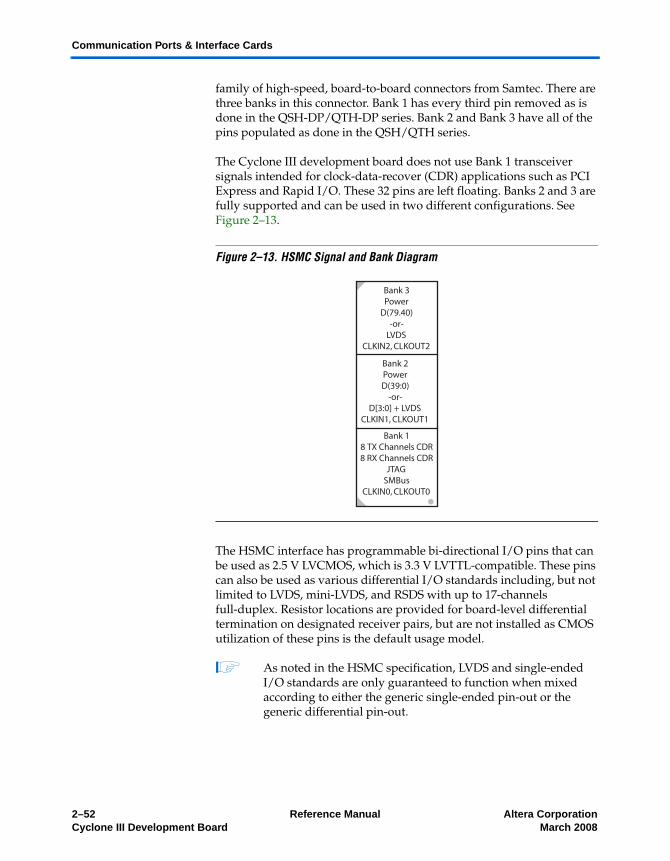
Communication Ports & Interface Cards
family of high-speed, board-to-board connectors from Samtec. There are three banks in this connector. Bank 1 has every third pin removed as is done in the QSH-DP/QTH-DP series. Bank 2 and Bank 3 have all of the pins populated as done in the QSH/QTH series.
The Cyclone III development board does not use Bank 1 transceiver signals intended for clock-data-recover (CDR) applications such as PCI Express and Rapid I/O. These 32 pins are left floating. Banks 2 and 3 are fully supported and can be used in two different configurations. See Figure 2–13.
Figure 2–13. HSMC Signal and Bank Diagram
The HSMC interface has programmable bi-directional I/O pins that can be used as 2.5 V LVCMOS, which is 3.3 V LVTTL-compatible. These pins can also be used as various differential I/O standards including, but not limited to LVDS, mini-LVDS, and RSDS with up to 17-channels full-duplex. Resistor locations are provided for board-level differential termination on designated receiver pairs, but are not installed as CMOS utilization of these pins is the default usage model.
1 As noted in the HSMC specification, LVDS and single-ended I/O standards are only guaranteed to function when mixed according to either the generic single-ended pin-out or the generic differential pin-out.
2–52 Reference Manual Altera CorporationCyclone III Development Board March 2008
Board Components
Table 2–47 lists the HSMC Port A interface signal names, descriptions, and I/O standard. Signal names and directions are relative to the Cyclone III FPGA, which is the HSMC host.
Table 2–47. HSMC Port A Interface Signal Names, Descriptions, and Type (Part 1 of 4)
BoardReference Description I/O Standard Schematic
Signal Name
Cyclone III Device Pin
Number
J8 pin 33 Management serial data 2.5 V HSMA_SDA AC1
J8 pin 34 Management serial clock 2.5 V HSMA_SCL AC3
J8 pin 35 JTAG clock signal 2.5 V FPGA_JTAG_TCK P5
J8 pin 36 JTAG mode select signal 2.5 V FPGA_JTAG_TMS P8
J8 pin 39 Dedicated CMOS clock out 2.5 V HSMA_CLK_OUT0 Y7
J8 pin 40 Dedicated CMOS clock in 1.8 V HSMA_CLK_IN0 AG14
J8 pin 41 Dedicated CMOS I/O bit 0 2.5 V HSMA_D0 AB6
J8 pin 42 Dedicated CMOS I/O bit 1 2.5 V HSMA_D1 AF2
J8 pin 43 Dedicated CMOS I/O bit 2 2.5 V HSMA_D2 AE3
J8 pin 44 Dedicated CMOS I/O bit 3 2.5 V HSMA_D3 AC5
J8 pin 47 LVDS TX or CMOS I/O bit 0 LVDS or 2.5 V HSMA_TX_P0 R7
J8 pin 48 LVDS RX or CMOS I/O bit 0 LVDS or 2.5 V HSMA_RX_P0 AB2
J8 pin 49 LVDS TX or CMOS I/O bit 0 LVDS or 2.5 V HSMA_TX_N0 R6
J8 pin 50 LVDS RX or CMOS I/O bit 0 LVDS or 2.5 V HSMA_RX_N0 AB1
J8 pin 53 LVDS TX bit 1p or CMOS I/O data 8 LVDS or 2.5 V HSMA_TX_P1 V4
J8 pin 54 LVDS RX bit 1p or CMOS I/O data 9 LVDS or 2.5 V HSMA_RX_P1 Y4
J8 pin 55 LVDS TX bit 1n or CMOS I/O data bit 10 LVDS or 2.5 V HSMA_TX_N1 V3
J8 pin 56 LVDS RX bit 1n or CMOS I/O data bit 11 LVDS or 2.5 V HSMA_RX_N1 Y3
J8 pin 59 LVDS TX bit 2p or CMOS I/O data bit 12 LVDS or 2.5 V HSMA_TX_P2 T4
J8 pin 60 LVDS RX bit 2p or CMOS I/O data bit 13 LVDS or 2.5 V HSMA_RX_P2 U3
J8 pin 61 LVDS TX bit 2n or CMOS I/O data bit 14 LVDS or 2.5 V HSMA_TX_N2 T3
J8 pin 62 LVDS RX bit 2n or CMOS I/O data bit 15 LVDS or 2.5 V HSMA_RX_N2 U4
J8 pin 65 LVDS TX bit 3p or CMOS I/O data bit 16 LVDS or 2.5 V HSMA_TX_P3 R3
J8 pin 66 LVDS RX bit 3p or CMOS I/O data bit 17 LVDS or 2.5 V HSMA_RX_P3 W2
J8 pin 67 LVDS TX bit 3n or CMOS I/O data bit 18 LVDS or 2.5 V HSMA_TX_N3 R4
J8 pin 68 LVDS RX bit 3n or CMOS I/O data bit 19 LVDS or 2.5 V HSMA_RX_N3 W1
J8 pin 71 LVDS TX bit 4p or CMOS I/O data bit 20 LVDS or 2.5 V HSMA_TX_P4 M8
J8 pin 72 LVDS RX bit 4p or CMOS I/O data bit 21 LVDS or 2.5 V HSMA_RX_P4 V2
J8 pin 73 LVDS TX or 4n CMOS I/O data bit 22 LVDS or 2.5 V HSMA_TX_N4 M7
Altera Corporation Reference Manual 2–53March 2008 Cyclone III Development Board
Communication Ports & Interface Cards
J8 pin 74 LVDS RX 4n or CMOS I/O data bit 23 LVDS or 2.5 V HSMA_RX_N4 V1
J8 pin 77 LVDS TX 5p or CMOS I/O data bit 24 LVDS or 2.5 V HSMA_TX_P5 P2
J8 pin 78 LVDS RX 5p or CMOS I/O data bit 25 LVDS or 2.5 V HSMA_RX_P5 U2
J8 pin 79 LVDS TX 5n or CMOS I/O data bit 26 LVDS or 2.5 V HSMA_TX_N5 P1
J8 pin 80 LVDS RX 5n or CMOS I/O data bit 27 LVDS or 2.5 V HSMA_RX_N5 U1
J8 pin 83 LVDS TX 6p or CMOS I/O data bit 28 LVDS or 2.5 V HSMA_TX_P6 M4
J8 pin 84 LVDS RX 6p or CMOS I/O data bit 29 LVDS or 2.5 V HSMA_RX_P6 U6
J8 pin 85 LVDS TX 6n or CMOS I/O data bit 30 LVDS or 2.5 V HSMA_TX_N6 M3
J8 pin 86 LVDS RX 6n or CMOS I/O data bit 31 LVDS or 2.5 V HSMA_RX_N6 U5
J8 pin 89 LVDS TX 7p or CMOS I/O data bit 32 LVDS or 2.5 V HSMA_TX_P7 M2
J8 pin 90 LVDS RX 7p or CMOS I/O data bit 33 LVDS or 2.5 V HSMA_RX_P7 R2
J8 pin 91 LVDS TX 7n or CMOS I/O data bit 34 LVDS or 2.5 V HSMA_TX_N7 M1
J8 pin 92 LVDS RX 7n or CMOS I/O data bit 35 LVDS or 2.5 V HSMA_RX_N7 R1
J8 pin 95 LVDS or CMOS clock out LVDS or 2.5 V HSMA_CLK_OUT_P1 G6
J8 pin 96 LVDS or CMOS clock in LVDS or 2.5 V HSMA_CLK_IN_P1 Y2
J8 pin 97 LVDS or CMOS clock out LVDS or 2.5 V HSMA_CLK_OUT_N1 G5
J8 pin 98 LVDS or CMOS clock in LVDS or 2.5 V HSMA_CLK_IN_N1 Y1
J8 pin 101 LVDS TX 8p or CMOS I/O data bit 40 LVDS or 2.5 V HSMA_TX_P8 L7
J8 pin 102 LVDS RX 8p or CMOS I/O data bit 41 LVDS or 2.5 V HSMA_RX_P8 N4
J8 pin 103 LVDS TX 8n or CMOS I/O data bit 42 LVDS or 2.5 V HSMA_TX_N8 L6
J8 pin 104 LVDS RX 8n or CMOS I/O data bit 43 LVDS or 2.5 V HSMA_RX_N8 N3
J8 pin 107 LVDS TX 9p or CMOS I/O data bit 44 LVDS or 2.5 V HSMA_TX_N9 L8
J8 pin 107 (is this suppose to be 108?)
LVDS RX 9p or CMOS I/O data bit 45 LVDS or 2.5 V HSMA_TX_P9 K8
J8 pin 108 (is this suppose to be 109?)
LVDS TX 9n or CMOS I/O data bit 46 LVDS or 2.5 V HSMA_RX_P9 L4
J8 pin 110 LVDS RX 9n or CMOS I/O data bit 47 LVDS or 2.5 V HSMA_RX_N9 L3
J8 pin 113 LVDS TX 10p or CMOS I/O data bit 48 LVDS or 2.5 V HSMA_TX_P10 K4
J8 pin 114 LVDS RX 10p or CMOS I/O data bit 49 LVDS or 2.5 V HSMA_RX_P10 L2
J8 pin 115 LVDS TX 10n or CMOS I/O data bit 50 LVDS or 2.5 V HSMA_TX_N10 K3
J8 pin 116 LVDS RX 10n or CMOS I/O data bit 51 LVDS or 2.5 V HSMA_RX_N10 L1
J8 pin 119 LVDS TX 11p or CMOS I/O data bit 52 LVDS or 2.5 V HSMA_TX_P11 J4
Table 2–47. HSMC Port A Interface Signal Names, Descriptions, and Type (Part 2 of 4)
BoardReference Description I/O Standard Schematic
Signal Name
Cyclone III Device Pin
Number
2–54 Reference Manual Altera CorporationCyclone III Development Board March 2008
Board Components
J8 pin 120 LVDS RX 11p or CMOS I/O data bit 53 LVDS or 2.5 V HSMA_RX_P11 K2
J8 pin 121 LVDS TX 11n or CMOS I/O data bit 54 LVDS or 2.5 V HSMA_TX_N11 J3
J8 pin 122 LVDS RX 11n or CMOS I/O data bit 55 LVDS or 2.5 V HSMA_RX_N11 K1
J8 pin 125 LVDS TX 12p or CMOS I/O data bit 56 LVDS or 2.5 V HSMA_TX_P12 J7
J8 pin 126 LVDS RX 12p or CMOS I/O data bit 57 LVDS or 2.5 V HSMA_RX_P12 J6
J8 pin 127 LVDS TX 12n or CMOS I/O data bit 58 LVDS or 2.5 V HSMA_TX_N12 K7
J8 pin 128 LVDS RX 12n or CMOS I/O data bit 59 LVDS or 2.5 V HSMA_RX_N12 J5
J8 pin 131 LVDS TX 13p or CMOS I/O data bit 60 LVDS or 2.5 V HSMA_TX_P13 G2
J8 pin 132 LVDS RX 13p or CMOS I/O data bit 61 LVDS or 2.5 V HSMA_RX_P13 H4
J8 pin 133 LVDS TX 13n or CMOS I/O data bit 62 LVDS or 2.5 V HSMA_TX_N13 G1
J8 pin 134 LVDS RX 13n or CMOS I/O data bit 63 LVDS or 2.5 V HSMA_RX_N13 H3
J8 pin 138 (is this suppose to be 137?)
LVDS TX 14p or CMOS I/O data bit 64 LVDS or 2.5 V HSMA_RX_P14 G4
J8 pin 139 (is this suppose to be 138?)
LVDS TX 14p or CMOS I/O data bit 65 LVDS or 2.5 V HSMA_TX_N14 F4
J8 pin 139 LVDS RX 14n or CMOS I/O data bit 66 LVDS or 2.5 V HSMA_TX_P14 F5
J8 pin 140 LVDS RX 14n or CMOS I/O data bit 67 LVDS or 2.5 V HSMA_RX_N14 G3
J8 pin 143 LVDS RX 15p or CMOS I/O data bit 68 LVDS or 2.5 V HSMA_TX_P15 E2
J8 pin 144 LVDS TX 15p or CMOS I/O data bit 69 LVDS or 2.5 V HSMA_RX_P15 F2
J8 pin 145 LVDS RX 15n or CMOS I/O data bit 70 LVDS or 2.5 V HSMA_TX_N15 E1
J8 pin 146 LVDS TX 15n or CMOS I/O data bit 71 LVDS or 2.5 V HSMA_RX_N15 F1
J8 pin 149 LVDS RX 16p or CMOS I/O data bit 72 LVDS or 2.5 V HSMA_TX_P16 D3
J8 pin 150 LVDS TX 16p or CMOS I/O data bit 73 LVDS or 2.5 V HSMA_RX_P16 E3
J8 pin 151 LVDS TX 16n or CMOS I/O data bit 74 LVDS or 2.5 V HSMA_TX_N16 C2
J8 pin 152 LVDS RX 16n or CMOS I/O data bit 75 LVDS or 2.5 V HSMA_RX_N16 F3
J8 pin 155 LVDS or CMOS clock out LVDS HSMA_CLK_OUT_P2 D2
J8 pin 156 LVDS or CMOS clock in LVDS HSMA_CLK_IN_P2 J2
J8 pin 157 LVDS or CMOS clock out 2.5 V HSMA_CLK_OUT_N2 D1
J8 pin 158 LVDS or CMOS clock in 2.5 V HSMA_CLK_IN_N2 J1
Table 2–47. HSMC Port A Interface Signal Names, Descriptions, and Type (Part 3 of 4)
BoardReference Description I/O Standard Schematic
Signal Name
Cyclone III Device Pin
Number
Altera Corporation Reference Manual 2–55March 2008 Cyclone III Development Board
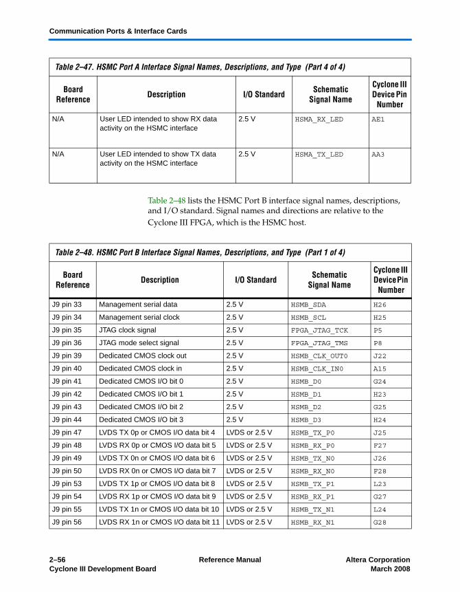
Communication Ports & Interface Cards
Table 2–48 lists the HSMC Port B interface signal names, descriptions, and I/O standard. Signal names and directions are relative to the Cyclone III FPGA, which is the HSMC host.
N/A User LED intended to show RX data activity on the HSMC interface
2.5 V HSMA_RX_LED AE1
N/A User LED intended to show TX data activity on the HSMC interface
2.5 V HSMA_TX_LED AA3
Table 2–47. HSMC Port A Interface Signal Names, Descriptions, and Type (Part 4 of 4)
BoardReference Description I/O Standard Schematic
Signal Name
Cyclone III Device Pin
Number
Table 2–48. HSMC Port B Interface Signal Names, Descriptions, and Type (Part 1 of 4)
BoardReference Description I/O Standard Schematic
Signal Name
Cyclone III Device Pin
Number
J9 pin 33 Management serial data 2.5 V HSMB_SDA H26
J9 pin 34 Management serial clock 2.5 V HSMB_SCL H25
J9 pin 35 JTAG clock signal 2.5 V FPGA_JTAG_TCK P5
J9 pin 36 JTAG mode select signal 2.5 V FPGA_JTAG_TMS P8
J9 pin 39 Dedicated CMOS clock out 2.5 V HSMB_CLK_OUT0 J22
J9 pin 40 Dedicated CMOS clock in 2.5 V HSMB_CLK_IN0 A15
J9 pin 41 Dedicated CMOS I/O bit 0 2.5 V HSMB_D0 G24
J9 pin 42 Dedicated CMOS I/O bit 1 2.5 V HSMB_D1 H23
J9 pin 43 Dedicated CMOS I/O bit 2 2.5 V HSMB_D2 G25
J9 pin 44 Dedicated CMOS I/O bit 3 2.5 V HSMB_D3 H24
J9 pin 47 LVDS TX 0p or CMOS I/O data bit 4 LVDS or 2.5 V HSMB_TX_P0 J25
J9 pin 48 LVDS RX 0p or CMOS I/O data bit 5 LVDS or 2.5 V HSMB_RX_P0 F27
J9 pin 49 LVDS TX 0n or CMOS I/O data bit 6 LVDS or 2.5 V HSMB_TX_N0 J26
J9 pin 50 LVDS RX 0n or CMOS I/O data bit 7 LVDS or 2.5 V HSMB_RX_N0 F28
J9 pin 53 LVDS TX 1p or CMOS I/O data bit 8 LVDS or 2.5 V HSMB_TX_P1 L23
J9 pin 54 LVDS RX 1p or CMOS I/O data bit 9 LVDS or 2.5 V HSMB_RX_P1 G27
J9 pin 55 LVDS TX 1n or CMOS I/O data bit 10 LVDS or 2.5 V HSMB_TX_N1 L24
J9 pin 56 LVDS RX 1n or CMOS I/O data bit 11 LVDS or 2.5 V HSMB_RX_N1 G28
2–56 Reference Manual Altera CorporationCyclone III Development Board March 2008
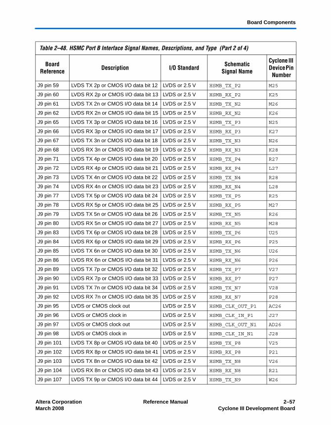
Board Components
J9 pin 59 LVDS TX 2p or CMOS I/O data bit 12 LVDS or 2.5 V HSMB_TX_P2 M25
J9 pin 60 LVDS RX 2p or CMOS I/O data bit 13 LVDS or 2.5 V HSMB_RX_P2 K25
J9 pin 61 LVDS TX 2n or CMOS I/O data bit 14 LVDS or 2.5 V HSMB_TX_N2 M26
J9 pin 62 LVDS RX 2n or CMOS I/O data bit 15 LVDS or 2.5 V HSMB_RX_N2 K26
J9 pin 65 LVDS TX 3p or CMOS I/O data bit 16 LVDS or 2.5 V HSMB_TX_P3 N25
J9 pin 66 LVDS RX 3p or CMOS I/O data bit 17 LVDS or 2.5 V HSMB_RX_P3 K27
J9 pin 67 LVDS TX 3n or CMOS I/O data bit 18 LVDS or 2.5 V HSMB_TX_N3 N26
J9 pin 68 LVDS RX 3n or CMOS I/O data bit 19 LVDS or 2.5 V HSMB_RX_N3 K28
J9 pin 71 LVDS TX 4p or CMOS I/O data bit 20 LVDS or 2.5 V HSMB_TX_P4 R27
J9 pin 72 LVDS RX 4p or CMOS I/O data bit 21 LVDS or 2.5 V HSMB_RX_P4 L27
J9 pin 73 LVDS TX 4n or CMOS I/O data bit 22 LVDS or 2.5 V HSMB_TX_N4 R28
J9 pin 74 LVDS RX 4n or CMOS I/O data bit 23 LVDS or 2.5 V HSMB_RX_N4 L28
J9 pin 77 LVDS TX 5p or CMOS I/O data bit 24 LVDS or 2.5 V HSMB_TX_P5 R25
J9 pin 78 LVDS RX 5p or CMOS I/O data bit 25 LVDS or 2.5 V HSMB_RX_P5 M27
J9 pin 79 LVDS TX 5n or CMOS I/O data bit 26 LVDS or 2.5 V HSMB_TX_N5 R26
J9 pin 80 LVDS RX 5n or CMOS I/O data bit 27 LVDS or 2.5 V HSMB_RX_N5 M28
J9 pin 83 LVDS TX 6p or CMOS I/O data bit 28 LVDS or 2.5 V HSMB_TX_P6 U25
J9 pin 84 LVDS RX 6p or CMOS I/O data bit 29 LVDS or 2.5 V HSMB_RX_P6 P25
J9 pin 85 LVDS TX 6n or CMOS I/O data bit 30 LVDS or 2.5 V HSMB_TX_N6 U26
J9 pin 86 LVDS RX 6n or CMOS I/O data bit 31 LVDS or 2.5 V HSMB_RX_N6 P26
J9 pin 89 LVDS TX 7p or CMOS I/O data bit 32 LVDS or 2.5 V HSMB_TX_P7 V27
J9 pin 90 LVDS RX 7p or CMOS I/O data bit 33 LVDS or 2.5 V HSMB_RX_P7 P27
J9 pin 91 LVDS TX 7n or CMOS I/O data bit 34 LVDS or 2.5 V HSMB_TX_N7 V28
J9 pin 92 LVDS RX 7n or CMOS I/O data bit 35 LVDS or 2.5 V HSMB_RX_N7 P28
J9 pin 95 LVDS or CMOS clock out LVDS or 2.5 V HSMB_CLK_OUT_P1 AC26
J9 pin 96 LVDS or CMOS clock in LVDS or 2.5 V HSMB_CLK_IN_P1 J27
J9 pin 97 LVDS or CMOS clock out LVDS or 2.5 V HSMB_CLK_OUT_N1 AD26
J9 pin 98 LVDS or CMOS clock in LVDS or 2.5 V HSMB_CLK_IN_N1 J28
J9 pin 101 LVDS TX 8p or CMOS I/O data bit 40 LVDS or 2.5 V HSMB_TX_P8 V25
J9 pin 102 LVDS RX 8p or CMOS I/O data bit 41 LVDS or 2.5 V HSMB_RX_P8 P21
J9 pin 103 LVDS TX 8n or CMOS I/O data bit 42 LVDS or 2.5 V HSMB_TX_N8 V26
J9 pin 104 LVDS RX 8n or CMOS I/O data bit 43 LVDS or 2.5 V HSMB_RX_N8 R21
J9 pin 107 LVDS TX 9p or CMOS I/O data bit 44 LVDS or 2.5 V HSMB_TX_N9 W26
Table 2–48. HSMC Port B Interface Signal Names, Descriptions, and Type (Part 2 of 4)
BoardReference Description I/O Standard Schematic
Signal Name
Cyclone III Device Pin
Number
Altera Corporation Reference Manual 2–57March 2008 Cyclone III Development Board
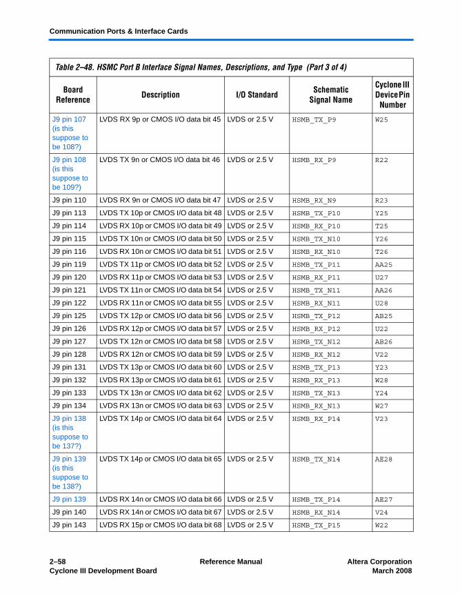
Communication Ports & Interface Cards
J9 pin 107 (is this suppose to be 108?)
LVDS RX 9p or CMOS I/O data bit 45 LVDS or 2.5 V HSMB_TX_P9 W25
J9 pin 108 (is this suppose to be 109?)
LVDS TX 9n or CMOS I/O data bit 46 LVDS or 2.5 V HSMB_RX_P9 R22
J9 pin 110 LVDS RX 9n or CMOS I/O data bit 47 LVDS or 2.5 V HSMB_RX_N9 R23
J9 pin 113 LVDS TX 10p or CMOS I/O data bit 48 LVDS or 2.5 V HSMB_TX_P10 Y25
J9 pin 114 LVDS RX 10p or CMOS I/O data bit 49 LVDS or 2.5 V HSMB_RX_P10 T25
J9 pin 115 LVDS TX 10n or CMOS I/O data bit 50 LVDS or 2.5 V HSMB_TX_N10 Y26
J9 pin 116 LVDS RX 10n or CMOS I/O data bit 51 LVDS or 2.5 V HSMB_RX_N10 T26
J9 pin 119 LVDS TX 11p or CMOS I/O data bit 52 LVDS or 2.5 V HSMB_TX_P11 AA25
J9 pin 120 LVDS RX 11p or CMOS I/O data bit 53 LVDS or 2.5 V HSMB_RX_P11 U27
J9 pin 121 LVDS TX 11n or CMOS I/O data bit 54 LVDS or 2.5 V HSMB_TX_N11 AA26
J9 pin 122 LVDS RX 11n or CMOS I/O data bit 55 LVDS or 2.5 V HSMB_RX_N11 U28
J9 pin 125 LVDS TX 12p or CMOS I/O data bit 56 LVDS or 2.5 V HSMB_TX_P12 AB25
J9 pin 126 LVDS RX 12p or CMOS I/O data bit 57 LVDS or 2.5 V HSMB_RX_P12 U22
J9 pin 127 LVDS TX 12n or CMOS I/O data bit 58 LVDS or 2.5 V HSMB_TX_N12 AB26
J9 pin 128 LVDS RX 12n or CMOS I/O data bit 59 LVDS or 2.5 V HSMB_RX_N12 V22
J9 pin 131 LVDS TX 13p or CMOS I/O data bit 60 LVDS or 2.5 V HSMB_TX_P13 Y23
J9 pin 132 LVDS RX 13p or CMOS I/O data bit 61 LVDS or 2.5 V HSMB_RX_P13 W28
J9 pin 133 LVDS TX 13n or CMOS I/O data bit 62 LVDS or 2.5 V HSMB_TX_N13 Y24
J9 pin 134 LVDS RX 13n or CMOS I/O data bit 63 LVDS or 2.5 V HSMB_RX_N13 W27
J9 pin 138 (is this suppose to be 137?)
LVDS TX 14p or CMOS I/O data bit 64 LVDS or 2.5 V HSMB_RX_P14 V23
J9 pin 139 (is this suppose to be 138?)
LVDS TX 14p or CMOS I/O data bit 65 LVDS or 2.5 V HSMB_TX_N14 AE28
J9 pin 139 LVDS RX 14n or CMOS I/O data bit 66 LVDS or 2.5 V HSMB_TX_P14 AE27
J9 pin 140 LVDS RX 14n or CMOS I/O data bit 67 LVDS or 2.5 V HSMB_RX_N14 V24
J9 pin 143 LVDS RX 15p or CMOS I/O data bit 68 LVDS or 2.5 V HSMB_TX_P15 W22
Table 2–48. HSMC Port B Interface Signal Names, Descriptions, and Type (Part 3 of 4)
BoardReference Description I/O Standard Schematic
Signal Name
Cyclone III Device Pin
Number
2–58 Reference Manual Altera CorporationCyclone III Development Board March 2008
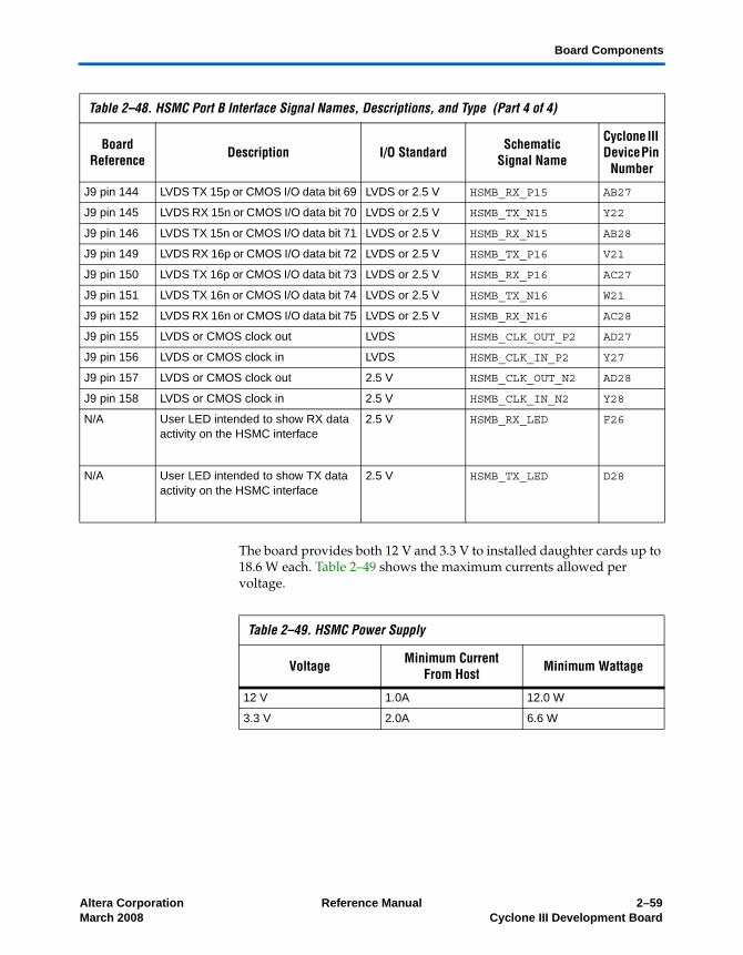
Board Components
The board provides both 12 V and 3.3 V to installed daughter cards up to 18.6 W each. Table 2–49 shows the maximum currents allowed per voltage.
J9 pin 144 LVDS TX 15p or CMOS I/O data bit 69 LVDS or 2.5 V HSMB_RX_P15 AB27
J9 pin 145 LVDS RX 15n or CMOS I/O data bit 70 LVDS or 2.5 V HSMB_TX_N15 Y22
J9 pin 146 LVDS TX 15n or CMOS I/O data bit 71 LVDS or 2.5 V HSMB_RX_N15 AB28
J9 pin 149 LVDS RX 16p or CMOS I/O data bit 72 LVDS or 2.5 V HSMB_TX_P16 V21
J9 pin 150 LVDS TX 16p or CMOS I/O data bit 73 LVDS or 2.5 V HSMB_RX_P16 AC27
J9 pin 151 LVDS TX 16n or CMOS I/O data bit 74 LVDS or 2.5 V HSMB_TX_N16 W21
J9 pin 152 LVDS RX 16n or CMOS I/O data bit 75 LVDS or 2.5 V HSMB_RX_N16 AC28
J9 pin 155 LVDS or CMOS clock out LVDS HSMB_CLK_OUT_P2 AD27
J9 pin 156 LVDS or CMOS clock in LVDS HSMB_CLK_IN_P2 Y27
J9 pin 157 LVDS or CMOS clock out 2.5 V HSMB_CLK_OUT_N2 AD28
J9 pin 158 LVDS or CMOS clock in 2.5 V HSMB_CLK_IN_N2 Y28
N/A User LED intended to show RX data activity on the HSMC interface
2.5 V HSMB_RX_LED F26
N/A User LED intended to show TX data activity on the HSMC interface
2.5 V HSMB_TX_LED D28
Table 2–48. HSMC Port B Interface Signal Names, Descriptions, and Type (Part 4 of 4)
BoardReference Description I/O Standard Schematic
Signal Name
Cyclone III Device Pin
Number
Table 2–49. HSMC Power Supply
Voltage Minimum Current From Host Minimum Wattage
12 V 1.0A 12.0 W
3.3 V 2.0A 6.6 W
Altera Corporation Reference Manual 2–59March 2008 Cyclone III Development Board
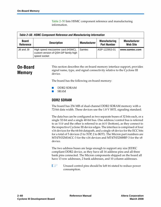
On-Board Memory
Table 2–50 lists HSMC component reference and manufacturing information.
On-Board Memory
This section describes the on-board memory interface support, provides signal name, type, and signal connectivity relative to the Cyclone III device.
The board has the following on-board memory:
■ DDR2 SDRAM■ SRAM
DDR2 SDRAM
The board has 256 MB of dual-channel DDR2 SDRAM memory with a 72-bit data width. These devices use the 1.8 V SSTL signaling standard.
The data bus can be configured as two separate buses of 32 bits each, or a single 32-bit and a single 40-bit bus. One address/control bus is referred to as TOP and the other is referred to as BOT (bottom), as they connect to the respective Cyclone III device edges. The interface is comprised of four x16 devices for the 64-bit datapath, and a single x8 device for the ECC bits for a total of 5 devices (3 to TOP, 2 to BOT). The Micron part numbers are MT47H32M16CC-3 for the x16 devices and MT47H32M8BP-3 for the x8 device.
The two address buses are large enough to support any size JEDEC compliant DDR2 device, as they have all 16 address pins and all three bank pins connected. The Micron components shipped on the board all have 13 row addresses, 2 bank addresses, and 10 column addresses.
1 Unused control pins should be left tri-stated to reduce power consumption.
Table 2–50. HSMC Component Reference and Manufacturing Information
Board Reference Description Manufacturer Manufacturing
Part NumberManufacturer
Web Site
J8 and J9 High speed mezzanine card (HSMC), custom version of QSH-DP family high speed socket
Samtec ASP-122953-01 www.samtec.com
2–60 Reference Manual Altera CorporationCyclone III Development Board March 2008
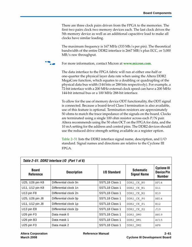
Board Components
There are three clock pairs driven from the FPGA to the memories. The first two pairs clock two memory devices each. The last clock drives the 5th memory device as well as an additional capacitive load to make all clocks have similar loading.
The maximum frequency is 167 MHz (333 Mb/s per pin). The theoretical bandwidth of the entire DDR2 interface is 2667 MB/s plus ECC, or 3,000 MB/s raw throughput.
f For more information, contact Micron at www.micron.com.
The data interface to the FPGA fabric will run at either one-half or one-quarter the physical layer data rate when using the Altera DDR2 MegaCore function, which equates to a doubling or quadrupling of the physical data bus width (144 bits or 288 bits respectively). For example, a 72-bit interface with a 200 MHz external clock speed can have a 200 MHz 144-bit internal bus or a 100 MHz 288-bit interface.
To allow for the use of memory device ODT functionality, the ODT signal is connected. Because a board-level Class I termination is also available, use of this feature is optional. Termination resistors are approximately 50 ohms to match the trace impedance of the signals on the board. Clocks are terminated using a single 100 ohm resistor across each P/N pair. Altera recommends using the 50 ohm OCT on the FPGA for data, and the 10 mA setting for the address and control pins. The DDR2 devices should use the reduced drive strength setting available as a register option.
Table 2–51 lists the DDR2 interface signal name, description, and I/O standard. Signal names and directions are relative to the Cyclone III FPGA.
Table 2–51. DDR2 Interface I/O (Part 1 of 6)
BoardReference Description I/O Standard Schematic
Signal Name
Cyclone III Device Pin
Number
U25, U26 pin K8 Differential clock 0n SSTL18 Class 1 DDR2_CK_N0 AF14
U11, U12 pin K8 Differential clock 1n SSTL18 Class 1 DDR2_CK_N1 G11
U13 pin F8 Differential clock 2n SSTL18 Class 1 DDR2_CK_N2 H19
U25, U26 pin J8 Differential clock 0p SSTL18 Class 1 DDR2_CK_P0 AE14
U11, U12 pin J8 Differential clock 1p SSTL18 Class 1 DDR2_CK_P1 H12
U13 pin E8 Differential clock 2p SSTL18 Class 1 DDR2_CK_P2 J19
U26 pin F3 Data mask 0 SSTL18 Class 1 DDR2_DM0 AH19
U26 pin B3 Data mask 1 SSTL18 Class 1 DDR2_DM1 AC15
U25 pin F3 Data mask 2 SSTL18 Class 1 DDR2_DM2 AF8
Altera Corporation Reference Manual 2–61March 2008 Cyclone III Development Board
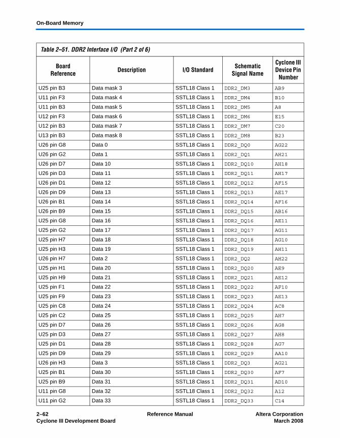
On-Board Memory
U25 pin B3 Data mask 3 SSTL18 Class 1 DDR2_DM3 AB9
U11 pin F3 Data mask 4 SSTL18 Class 1 DDR2_DM4 B10
U11 pin B3 Data mask 5 SSTL18 Class 1 DDR2_DM5 A8
U12 pin F3 Data mask 6 SSTL18 Class 1 DDR2_DM6 E15
U12 pin B3 Data mask 7 SSTL18 Class 1 DDR2_DM7 C20
U13 pin B3 Data mask 8 SSTL18 Class 1 DDR2_DM8 B23
U26 pin G8 Data 0 SSTL18 Class 1 DDR2_DQ0 AG22
U26 pin G2 Data 1 SSTL18 Class 1 DDR2_DQ1 AH21
U26 pin D7 Data 10 SSTL18 Class 1 DDR2_DQ10 AH18
U26 pin D3 Data 11 SSTL18 Class 1 DDR2_DQ11 AH17
U26 pin D1 Data 12 SSTL18 Class 1 DDR2_DQ12 AF15
U26 pin D9 Data 13 SSTL18 Class 1 DDR2_DQ13 AE17
U26 pin B1 Data 14 SSTL18 Class 1 DDR2_DQ14 AF16
U26 pin B9 Data 15 SSTL18 Class 1 DDR2_DQ15 AB16
U25 pin G8 Data 16 SSTL18 Class 1 DDR2_DQ16 AE11
U25 pin G2 Data 17 SSTL18 Class 1 DDR2_DQ17 AG11
U25 pin H7 Data 18 SSTL18 Class 1 DDR2_DQ18 AG10
U25 pin H3 Data 19 SSTL18 Class 1 DDR2_DQ19 AH11
U26 pin H7 Data 2 SSTL18 Class 1 DDR2_DQ2 AH22
U25 pin H1 Data 20 SSTL18 Class 1 DDR2_DQ20 AE9
U25 pin H9 Data 21 SSTL18 Class 1 DDR2_DQ21 AE12
U25 pin F1 Data 22 SSTL18 Class 1 DDR2_DQ22 AF10
U25 pin F9 Data 23 SSTL18 Class 1 DDR2_DQ23 AE13
U25 pin C8 Data 24 SSTL18 Class 1 DDR2_DQ24 AC8
U25 pin C2 Data 25 SSTL18 Class 1 DDR2_DQ25 AH7
U25 pin D7 Data 26 SSTL18 Class 1 DDR2_DQ26 AG8
U25 pin D3 Data 27 SSTL18 Class 1 DDR2_DQ27 AH8
U25 pin D1 Data 28 SSTL18 Class 1 DDR2_DQ28 AG7
U25 pin D9 Data 29 SSTL18 Class 1 DDR2_DQ29 AA10
U26 pin H3 Data 3 SSTL18 Class 1 DDR2_DQ3 AG21
U25 pin B1 Data 30 SSTL18 Class 1 DDR2_DQ30 AF7
U25 pin B9 Data 31 SSTL18 Class 1 DDR2_DQ31 AD10
U11 pin G8 Data 32 SSTL18 Class 1 DDR2_DQ32 A12
U11 pin G2 Data 33 SSTL18 Class 1 DDR2_DQ33 C14
Table 2–51. DDR2 Interface I/O (Part 2 of 6)
BoardReference Description I/O Standard Schematic
Signal Name
Cyclone III Device Pin
Number
2–62 Reference Manual Altera CorporationCyclone III Development Board March 2008
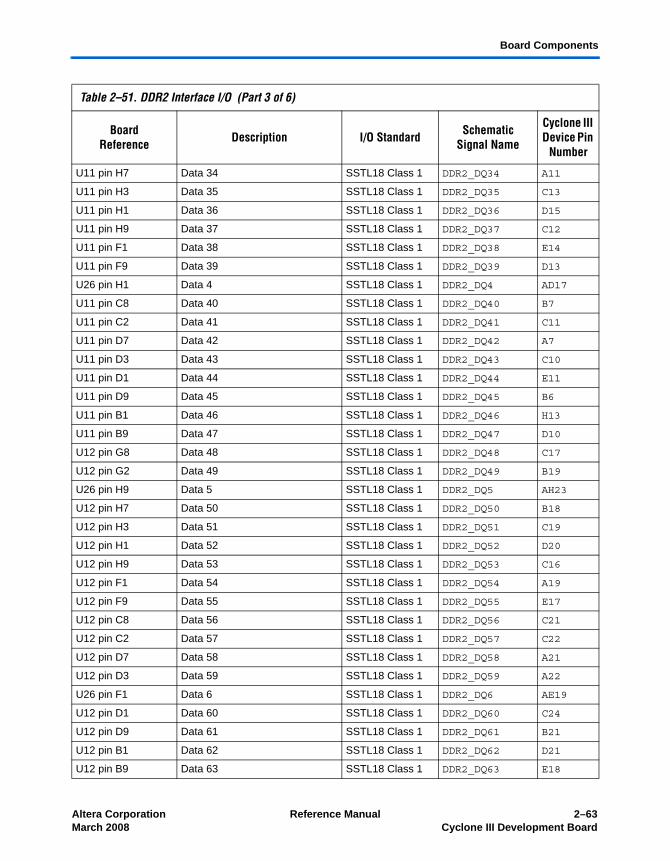
Board Components
U11 pin H7 Data 34 SSTL18 Class 1 DDR2_DQ34 A11
U11 pin H3 Data 35 SSTL18 Class 1 DDR2_DQ35 C13
U11 pin H1 Data 36 SSTL18 Class 1 DDR2_DQ36 D15
U11 pin H9 Data 37 SSTL18 Class 1 DDR2_DQ37 C12
U11 pin F1 Data 38 SSTL18 Class 1 DDR2_DQ38 E14
U11 pin F9 Data 39 SSTL18 Class 1 DDR2_DQ39 D13
U26 pin H1 Data 4 SSTL18 Class 1 DDR2_DQ4 AD17
U11 pin C8 Data 40 SSTL18 Class 1 DDR2_DQ40 B7
U11 pin C2 Data 41 SSTL18 Class 1 DDR2_DQ41 C11
U11 pin D7 Data 42 SSTL18 Class 1 DDR2_DQ42 A7
U11 pin D3 Data 43 SSTL18 Class 1 DDR2_DQ43 C10
U11 pin D1 Data 44 SSTL18 Class 1 DDR2_DQ44 E11
U11 pin D9 Data 45 SSTL18 Class 1 DDR2_DQ45 B6
U11 pin B1 Data 46 SSTL18 Class 1 DDR2_DQ46 H13
U11 pin B9 Data 47 SSTL18 Class 1 DDR2_DQ47 D10
U12 pin G8 Data 48 SSTL18 Class 1 DDR2_DQ48 C17
U12 pin G2 Data 49 SSTL18 Class 1 DDR2_DQ49 B19
U26 pin H9 Data 5 SSTL18 Class 1 DDR2_DQ5 AH23
U12 pin H7 Data 50 SSTL18 Class 1 DDR2_DQ50 B18
U12 pin H3 Data 51 SSTL18 Class 1 DDR2_DQ51 C19
U12 pin H1 Data 52 SSTL18 Class 1 DDR2_DQ52 D20
U12 pin H9 Data 53 SSTL18 Class 1 DDR2_DQ53 C16
U12 pin F1 Data 54 SSTL18 Class 1 DDR2_DQ54 A19
U12 pin F9 Data 55 SSTL18 Class 1 DDR2_DQ55 E17
U12 pin C8 Data 56 SSTL18 Class 1 DDR2_DQ56 C21
U12 pin C2 Data 57 SSTL18 Class 1 DDR2_DQ57 C22
U12 pin D7 Data 58 SSTL18 Class 1 DDR2_DQ58 A21
U12 pin D3 Data 59 SSTL18 Class 1 DDR2_DQ59 A22
U26 pin F1 Data 6 SSTL18 Class 1 DDR2_DQ6 AE19
U12 pin D1 Data 60 SSTL18 Class 1 DDR2_DQ60 C24
U12 pin D9 Data 61 SSTL18 Class 1 DDR2_DQ61 B21
U12 pin B1 Data 62 SSTL18 Class 1 DDR2_DQ62 D21
U12 pin B9 Data 63 SSTL18 Class 1 DDR2_DQ63 E18
Table 2–51. DDR2 Interface I/O (Part 3 of 6)
BoardReference Description I/O Standard Schematic
Signal Name
Cyclone III Device Pin
Number
Altera Corporation Reference Manual 2–63March 2008 Cyclone III Development Board
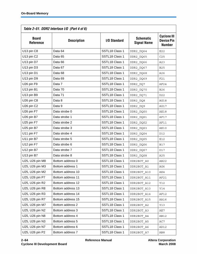
On-Board Memory
U13 pin C8 Data 64 SSTL18 Class 1 DDR2_DQ64 E22
U13 pin C2 Data 65 SSTL18 Class 1 DDR2_DQ65 C25
U13 pin D7 Data 66 SSTL18 Class 1 DDR2_DQ66 A23
U13 pin D3 Data 67 SSTL18 Class 1 DDR2_DQ67 B25
U13 pin D1 Data 68 SSTL18 Class 1 DDR2_DQ68 A26
U13 pin D9 Data 69 SSTL18 Class 1 DDR2_DQ69 F21
U26 pin F9 Data 7 SSTL18 Class 1 DDR2_DQ7 AF24
U13 pin B1 Data 70 SSTL18 Class 1 DDR2_DQ70 B26
U13 pin B9 Data 71 SSTL18 Class 1 DDR2_DQ71 D22
U26 pin C8 Data 8 SSTL18 Class 1 DDR2_DQ8 AG18
U26 pin C2 Data 9 SSTL18 Class 1 DDR2_DQ9 AG17
U26 pin F7 Data strobe 0 SSTL18 Class 1 DDR2_DQS0 AE18
U26 pin B7 Data strobe 1 SSTL18 Class 1 DDR2_DQS1 AF17
U25 pin F7 Data strobe 2 SSTL18 Class 1 DDR2_DQS2 AF11
U25 pin B7 Data strobe 3 SSTL18 Class 1 DDR2_DQS3 AE10
U11 pin F7 Data strobe 4 SSTL18 Class 1 DDR2_DQS4 D12
U11 pin B7 Data strobe 5 SSTL18 Class 1 DDR2_DQS5 E12
U12 pin F7 Data strobe 6 SSTL18 Class 1 DDR2_DQS6 B17
U12 pin B7 Data strobe 7 SSTL18 Class 1 DDR2_DQS7 D17
U13 pin B7 Data strobe 8 SSTL18 Class 1 DDR2_DQS8 A25
U25, U26 pin M8 Bottom address 0 SSTL18 Class 1 DDR2BOT_A0 AB22
U25, U26 pin M3 Bottom address 1 SSTL18 Class 1 DDR2BOT_A1 AG6
U25, U26 pin M2 Bottom address 10 SSTL18 Class 1 DDR2BOT_A10 AE4
U25, U26 pin P7 Bottom address 11 SSTL18 Class 1 DDR2BOT_A11 AF21
U25, U26 pin R2 Bottom address 12 SSTL18 Class 1 DDR2BOT_A12 Y12
U25, U26 pin R8 Bottom address 13 SSTL18 Class 1 DDR2BOT_A13 Y14
U25, U26 pin R3 Bottom address 14 SSTL18 Class 1 DDR2BOT_A14 AF12
U25, U26 pin R7 Bottom address 15 SSTL18 Class 1 DDR2BOT_A15 AA16
U25, U26 pin M7 Bottom address 2 SSTL18 Class 1 DDR2BOT_A2 Y13
U25, U26 pin N2 Bottom address 3 SSTL18 Class 1 DDR2BOT_A3 AE7
U25, U26 pin N8 Bottom address 4 SSTL18 Class 1 DDR2BOT_A4 AB12
U25, U26 pin N3 Bottom address 5 SSTL18 Class 1 DDR2BOT_A5 AC7
U25, U26 pin N7 Bottom address 6 SSTL18 Class 1 DDR2BOT_A6 AD12
U25, U26 pin P2 Bottom address 7 SSTL18 Class 1 DDR2BOT_A7 AB8
Table 2–51. DDR2 Interface I/O (Part 4 of 6)
BoardReference Description I/O Standard Schematic
Signal Name
Cyclone III Device Pin
Number
2–64 Reference Manual Altera CorporationCyclone III Development Board March 2008
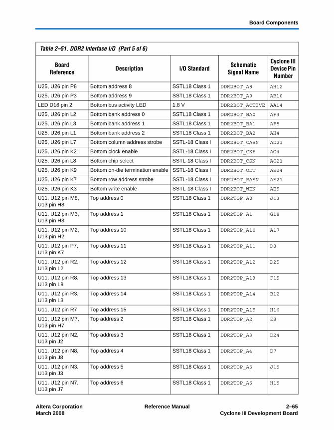
Board Components
U25, U26 pin P8 Bottom address 8 SSTL18 Class 1 DDR2BOT_A8 AH12
U25, U26 pin P3 Bottom address 9 SSTL18 Class 1 DDR2BOT_A9 AB10
LED D16 pin 2 Bottom bus activity LED 1.8 V DDR2BOT_ACTIVE AA14
U25, U26 pin L2 Bottom bank address 0 SSTL18 Class 1 DDR2BOT_BA0 AF3
U25, U26 pin L3 Bottom bank address 1 SSTL18 Class 1 DDR2BOT_BA1 AF5
U25, U26 pin L1 Bottom bank address 2 SSTL18 Class 1 DDR2BOT_BA2 AH4
U25, U26 pin L7 Bottom column address strobe SSTL-18 Class I DDR2BOT_CASN AD21
U25, U26 pin K2 Bottom clock enable SSTL-18 Class I DDR2BOT_CKE AG4
U25, U26 pin L8 Bottom chip select SSTL-18 Class I DDR2BOT_CSN AC21
U25, U26 pin K9 Bottom on-die termination enable SSTL-18 Class I DDR2BOT_ODT AE24
U25, U26 pin K7 Bottom row address strobe SSTL-18 Class I DDR2BOT_RASN AE21
U25, U26 pin K3 Bottom write enable SSTL-18 Class I DDR2BOT_WEN AE5
U11, U12 pin M8, U13 pin H8
Top address 0 SSTL18 Class 1 DDR2TOP_A0 J13
U11, U12 pin M3, U13 pin H3
Top address 1 SSTL18 Class 1 DDR2TOP_A1 G18
U11, U12 pin M2, U13 pin H2
Top address 10 SSTL18 Class 1 DDR2TOP_A10 A17
U11, U12 pin P7, U13 pin K7
Top address 11 SSTL18 Class 1 DDR2TOP_A11 D8
U11, U12 pin R2, U13 pin L2
Top address 12 SSTL18 Class 1 DDR2TOP_A12 D25
U11, U12 pin R8, U13 pin L8
Top address 13 SSTL18 Class 1 DDR2TOP_A13 F15
U11, U12 pin R3, U13 pin L3
Top address 14 SSTL18 Class 1 DDR2TOP_A14 B12
U11, U12 pin R7 Top address 15 SSTL18 Class 1 DDR2TOP_A15 H16
U11, U12 pin M7, U13 pin H7
Top address 2 SSTL18 Class 1 DDR2TOP_A2 E8
U11, U12 pin N2, U13 pin J2
Top address 3 SSTL18 Class 1 DDR2TOP_A3 D24
U11, U12 pin N8, U13 pin J8
Top address 4 SSTL18 Class 1 DDR2TOP_A4 D7
U11, U12 pin N3, U13 pin J3
Top address 5 SSTL18 Class 1 DDR2TOP_A5 J15
U11, U12 pin N7, U13 pin J7
Top address 6 SSTL18 Class 1 DDR2TOP_A6 H15
Table 2–51. DDR2 Interface I/O (Part 5 of 6)
BoardReference Description I/O Standard Schematic
Signal Name
Cyclone III Device Pin
Number
Altera Corporation Reference Manual 2–65March 2008 Cyclone III Development Board
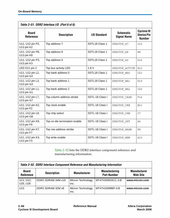
On-Board Memory
Table 2–52 lists the DDR2 interface component reference and manufacturing information.
U11, U12 pin P2, U13 pin K2
Top address 7 SSTL18 Class 1 DDR2TOP_A7 J16
U11, U12 pin P8, U13 pin K8
Top address 8 SSTL18 Class 1 DDR2TOP_A8 H8
U11, U12 pin P3, U13 pin K3
Top address 9 SSTL18 Class 1 DDR2TOP_A9 D16
LED D11 pin 2 Top bus activity LED 1.8 V DDR2TOP_ACTIVE E10
U11, U12 pin L2, U13 pin G2
Top bank address 0 SSTL18 Class 1 DDR2TOP_BA0 C23
U11, U12 pin L3, U13 pin G3
Top bank address 1 SSTL18 Class 1 DDR2TOP_BA1 D19
U11, U12 pin L1, U13 pin G1
Top bank address 2 SSTL18 Class 1 DDR2TOP_BA2 C26
U11, U12 pin L7, U13 pin G7
Top column address strobe SSTL-18 Class I DDR2TOP_CASN F14
U11, U12 pin K2, U13 pin F2
Top clock enable SSTL-18 Class I DDR2TOP_CKE E21
U11, U12 pin L8, U13 pin G8
Top chip select SSTL-18 Class I DDR2TOP_CSN C7
U11, U12 pin K9, U13 pin F9
Top on-die termination enable SSTL-18 Class I DDR2TOP_ODT A6
U11, U12 pin K7, U13 pin F7
Top row address strobe SSTL-18 Class I DDR2TOP_RASN F8
U11, U12 pin K3, U13 pin F3
Top write enable SSTL-18 Class I DDR2TOP_WEN A10
Table 2–51. DDR2 Interface I/O (Part 6 of 6)
BoardReference Description I/O Standard Schematic
Signal Name
Cyclone III Device Pin
Number
Table 2–52. DDR2 Interface Component Reference and Manufacturing Information
Board Reference Description Manufacturer Manufacturing
Part NumberManufacturer
Web Site
U11, U12, U25, U26
DDR2 SDRAM 34M x16 Micron Technology, Inc.
MT47H32M16CC-3:B www.micron.com
U13 DDR2 SDRAM 32M x8 Micron Technology, Inc.
MT47H32M8BP-3:B www.micron.com
2–66 Reference Manual Altera CorporationCyclone III Development Board March 2008
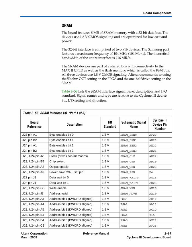
Board Components
SRAM
The board features 8 MB of SRAM memory with a 32-bit data bus. The devices use 1.8 V CMOS signaling and are optimized for low cost and power.
The 32-bit interface is comprised of two x16 devices. The Samsung part features a maximum frequency of 104 MHz (104 Mb/s). The theoretical bandwidth of the entire interface is 416 MB/s.
The SRAM devices are part of a shared bus with connectivity to the MAX II CPLD as well as the flash memory, which is called the FSM bus. All three devices use 1.8 V CMOS signaling. Altera recommends to using the 50 ohm OCT setting on the FPGA and the one-half drive setting on the SRAM.
Table 2–53 lists the SRAM interface signal name, description, and I/O standard. Signal names and type are relative to the Cyclone III device, i.e., I/O setting and direction.
Table 2–53. SRAM Interface I/O (Part 1 of 3)
BoardReference Description I/O
StandardSchematic Signal
Name
Cyclone III Device Pin
Number
U23 pin A1 Byte enables bit 0 1.8 V SRAM_BEN0 AF20
U23 pin B2 Byte enables bit 1 1.8 V SRAM_BEN1 AH26
U24 pin A1 Byte enables bit 2 1.8 V SRAM_BEN2 AE22
U24 pin B2 Byte enables bit 3 1.8 V SRAM_BEN3 AB21
U23, U24 pin J2 Clock (drives two memories) 1.8 V SRAM_CLK AD22
U23, U24 pin B5 Chip select 1.8 V SRAM_CSN AB19
U23, U24 pin A2 Output enable 1.8 V SRAM_OEN AD25
U23, U24 pin A6 Power save /MRS set pin 1.8 V SRAM_PSN B4
U23 pin J1 Data wait bit 0 1.8 V SRAM_WAIT0 AG15
U24 pin J1 Data wait bit 1 1.8 V SRAM_WAIT1 AH25
U23, U24 pin G5 Write enable 1.8 V SRAM_WEN AE25
U23, U24 pin J3 Address valid 1.8 V SRAM_ADVN AA19
U23, U24 pin A3 Address bit 1 (DWORD aligned) 1.8 V FSA1 AH10
U23, U24 pin A4 Address bit 2 (DWORD aligned) 1.8 V FSA2 AA13
U23, U24 pin A5 Address bit 3 (DWORD aligned) 1.8 V FSA3 AC10
U23, U24 pin B3 Address bit 4 (DWORD aligned) 1.8 V FSA4 Y15
U23, U24 pin B4 Address bit 5 (DWORD aligned) 1.8 V FSA5 AF22
U23, U24 pin C3 Address bit 6 (DWORD aligned) 1.8 V FSA6 AF26
Altera Corporation Reference Manual 2–67March 2008 Cyclone III Development Board
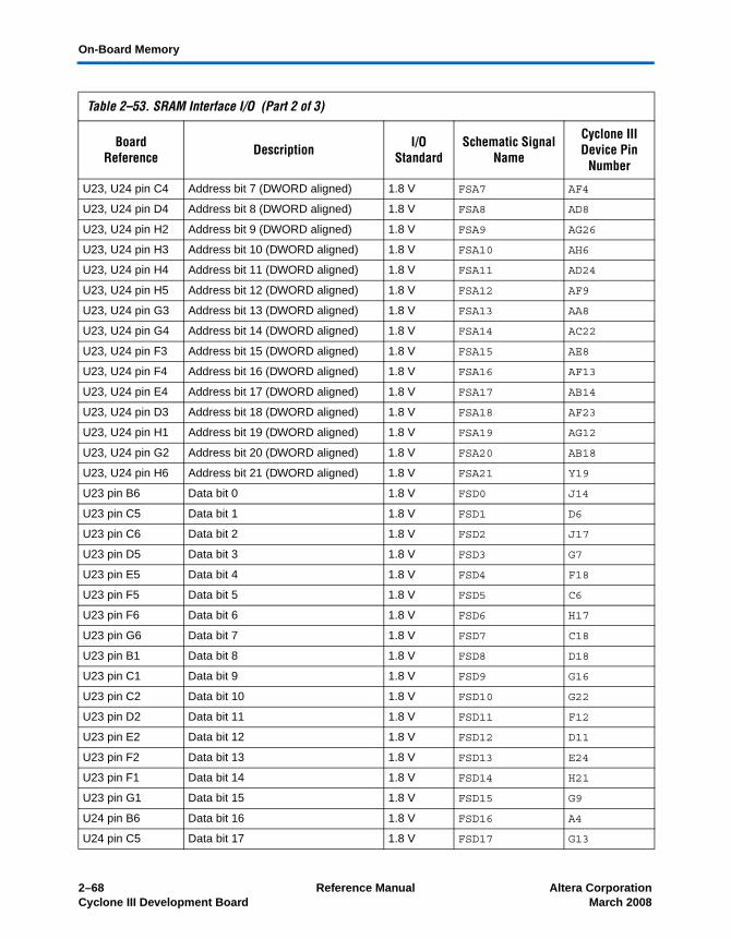
On-Board Memory
U23, U24 pin C4 Address bit 7 (DWORD aligned) 1.8 V FSA7 AF4
U23, U24 pin D4 Address bit 8 (DWORD aligned) 1.8 V FSA8 AD8
U23, U24 pin H2 Address bit 9 (DWORD aligned) 1.8 V FSA9 AG26
U23, U24 pin H3 Address bit 10 (DWORD aligned) 1.8 V FSA10 AH6
U23, U24 pin H4 Address bit 11 (DWORD aligned) 1.8 V FSA11 AD24
U23, U24 pin H5 Address bit 12 (DWORD aligned) 1.8 V FSA12 AF9
U23, U24 pin G3 Address bit 13 (DWORD aligned) 1.8 V FSA13 AA8
U23, U24 pin G4 Address bit 14 (DWORD aligned) 1.8 V FSA14 AC22
U23, U24 pin F3 Address bit 15 (DWORD aligned) 1.8 V FSA15 AE8
U23, U24 pin F4 Address bit 16 (DWORD aligned) 1.8 V FSA16 AF13
U23, U24 pin E4 Address bit 17 (DWORD aligned) 1.8 V FSA17 AB14
U23, U24 pin D3 Address bit 18 (DWORD aligned) 1.8 V FSA18 AF23
U23, U24 pin H1 Address bit 19 (DWORD aligned) 1.8 V FSA19 AG12
U23, U24 pin G2 Address bit 20 (DWORD aligned) 1.8 V FSA20 AB18
U23, U24 pin H6 Address bit 21 (DWORD aligned) 1.8 V FSA21 Y19
U23 pin B6 Data bit 0 1.8 V FSD0 J14
U23 pin C5 Data bit 1 1.8 V FSD1 D6
U23 pin C6 Data bit 2 1.8 V FSD2 J17
U23 pin D5 Data bit 3 1.8 V FSD3 G7
U23 pin E5 Data bit 4 1.8 V FSD4 F18
U23 pin F5 Data bit 5 1.8 V FSD5 C6
U23 pin F6 Data bit 6 1.8 V FSD6 H17
U23 pin G6 Data bit 7 1.8 V FSD7 C18
U23 pin B1 Data bit 8 1.8 V FSD8 D18
U23 pin C1 Data bit 9 1.8 V FSD9 G16
U23 pin C2 Data bit 10 1.8 V FSD10 G22
U23 pin D2 Data bit 11 1.8 V FSD11 F12
U23 pin E2 Data bit 12 1.8 V FSD12 D11
U23 pin F2 Data bit 13 1.8 V FSD13 E24
U23 pin F1 Data bit 14 1.8 V FSD14 H21
U23 pin G1 Data bit 15 1.8 V FSD15 G9
U24 pin B6 Data bit 16 1.8 V FSD16 A4
U24 pin C5 Data bit 17 1.8 V FSD17 G13
Table 2–53. SRAM Interface I/O (Part 2 of 3)
BoardReference Description I/O
StandardSchematic Signal
Name
Cyclone III Device Pin
Number
2–68 Reference Manual Altera CorporationCyclone III Development Board March 2008
Board Components
Figure 2–14 illustrates the latency for both fixed and variable modes of operation. For asynchronous accesses, each of the two devices has its own WAIT pin wired to the Cyclone III device.
f For Samsung SRAM pin definitions, data sheet, and other related documentation, refer to the Samsung website at www.samsung.com.
U24 pin C6 Data bit 18 1.8 V FSD18 H14
U24 pin D5 Data bit 19 1.8 V FSD19 B8
U24 pin E5 Data bit 20 1.8 V FSD20 C8
U24 pin F5 Data bit 21 1.8 V FSD21 F7
U24 pin F6 Data bit 22 1.8 V FSD22 B11
U24 pin G6 Data bit 23 1.8 V FSD23 B22
U24 pin B1 Data bit 24 1.8 V FSD24 A18
U24 pin C1 Data bit 25 1.8 V FSD25 G8
U24 pin C2 Data bit 26 1.8 V FSD26 J12
U24 pin D2 Data bit 27 1.8 V FSD27 D9
U24 pin E2 Data bit 28 1.8 V FSD28 C9
U24 pin F2 Data bit 29 1.8 V FSD29 E7
U24 pin F1 Data bit 30 1.8 V FSD30 H10
U24 pin G1 Data bit 31 1.8 V FSD31 J10
Table 2–53. SRAM Interface I/O (Part 3 of 3)
BoardReference Description I/O
StandardSchematic Signal
Name
Cyclone III Device Pin
Number
Altera Corporation Reference Manual 2–69March 2008 Cyclone III Development Board
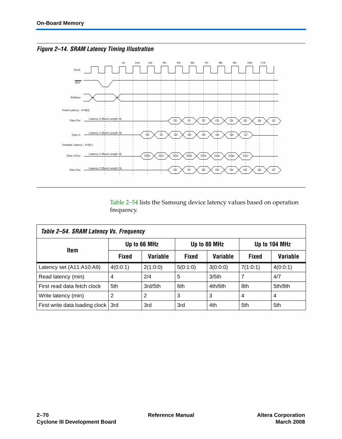
On-Board Memory
Figure 2–14. SRAM Latency Timing Illustration
Table 2–54 lists the Samsung device latency values based on operation frequency.
Table 2–54. SRAM Latency Vs. Frequency
ItemUp to 66 MHz Up to 80 MHz Up to 104 MHz
Fixed Variable Fixed Variable Fixed Variable
Latency set (A11:A10:A9) 4(0:0:1) 2(1:0:0) 5(0:1:0) 3(0:0:0) 7(1:0:1) 4(0:0:1)
Read latency (min) 4 2/4 5 3/5th 7 4/7
First read data fetch clock 5th 3rd/5th 6th 4th/6th 8th 5th/8th
Write latency (min) 2 2 3 3 4 4
First write data loading clock 3rd 3rd 3rd 4th 5th 5th
2–70 Reference Manual Altera CorporationCyclone III Development Board March 2008
Board Components
Figures 2–15 and 2–16 show the Samsung device read and write access waveforms.
Figure 2–15. SRAM Read Timing Waveforms
Figure 2–16. SRAM Write Timing Waveforms
Altera Corporation Reference Manual 2–71March 2008 Cyclone III Development Board
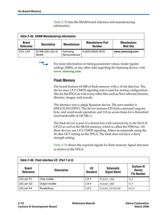
On-Board Memory
Table 2–55 lists the SRAM board reference and manufacturing information.
f For more information on timing parameter values, mode register settings (MRS), or any other data regarding the Samsung device, visit www. samsung.com.
Flash Memory
The board features 64 MB of flash memory with a 16-bit data bus. The device uses 1.8 V CMOS signaling and is used for storing configuration files for the FPGA as well as any other files such as Nios software binaries, libraries, images, and sounds.
The interface uses a single Spansion device. The part number is S29GL512N11FFIV1. The device features CFI flash command support, byte- and word-mode operation, and 110 ns access times for a theoretical read bandwidth of 145 Mb/s.
The flash device is part of a shared bus with connectivity to the MAX II CPLD as well as the SRAM memory, which is called the FSM bus. All three devices use 1.8 V CMOS signaling. Altera recommends using the 50 ohm OCT setting on the FPGA. The flash does not have a drive strength setting.
Table 2–56 shows the required signals for flash memory. Signal direction is relative to the FPGA.
Table 2–55. SRAM Manufacturing Information
Board Reference Description Manufacturer Manufacturer Part
NumberManufacturer
Web Site
U23, U24 32 MB (2M x16) of SRAM
Samsung Semiconductor
K1B3216B2E-BI70 www.samsung.com
Table 2–56. Flash Interface I/O (Part 1 of 3)
BoardReference Description I/O
StandardSchematic
Signal Name
Cyclone III Device
Pin Number
U31 pin F2 Chip enable 1.8 V FLASH_CEN Y16
U31 pin G2 Output enable 1.8 V FLASH_OEN Y17
U31 pin A4 Ready/busy 1.8 V FLASH_RDYBSYN AG25
2–72 Reference Manual Altera CorporationCyclone III Development Board March 2008
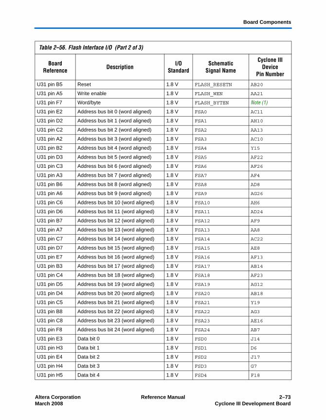
Board Components
U31 pin B5 Reset 1.8 V FLASH_RESETN AB20
U31 pin A5 Write enable 1.8 V FLASH_WEN AA21
U31 pin F7 Word/byte 1.8 V FLASH_BYTEN Note (1)
U31 pin E2 Address bus bit 0 (word aligned) 1.8 V FSA0 AC11
U31 pin D2 Address bus bit 1 (word aligned) 1.8 V FSA1 AH10
U31 pin C2 Address bus bit 2 (word aligned) 1.8 V FSA2 AA13
U31 pin A2 Address bus bit 3 (word aligned) 1.8 V FSA3 AC10
U31 pin B2 Address bus bit 4 (word aligned) 1.8 V FSA4 Y15
U31 pin D3 Address bus bit 5 (word aligned) 1.8 V FSA5 AF22
U31 pin C3 Address bus bit 6 (word aligned) 1.8 V FSA6 AF26
U31 pin A3 Address bus bit 7 (word aligned) 1.8 V FSA7 AF4
U31 pin B6 Address bus bit 8 (word aligned) 1.8 V FSA8 AD8
U31 pin A6 Address bus bit 9 (word aligned) 1.8 V FSA9 AG26
U31 pin C6 Address bus bit 10 (word aligned) 1.8 V FSA10 AH6
U31 pin D6 Address bus bit 11 (word aligned) 1.8 V FSA11 AD24
U31 pin B7 Address bus bit 12 (word aligned) 1.8 V FSA12 AF9
U31 pin A7 Address bus bit 13 (word aligned) 1.8 V FSA13 AA8
U31 pin C7 Address bus bit 14 (word aligned) 1.8 V FSA14 AC22
U31 pin D7 Address bus bit 15 (word aligned) 1.8 V FSA15 AE8
U31 pin E7 Address bus bit 16 (word aligned) 1.8 V FSA16 AF13
U31 pin B3 Address bus bit 17 (word aligned) 1.8 V FSA17 AB14
U31 pin C4 Address bus bit 18 (word aligned) 1.8 V FSA18 AF23
U31 pin D5 Address bus bit 19 (word aligned) 1.8 V FSA19 AG12
U31 pin D4 Address bus bit 20 (word aligned) 1.8 V FSA20 AB18
U31 pin C5 Address bus bit 21 (word aligned) 1.8 V FSA21 Y19
U31 pin B8 Address bus bit 22 (word aligned) 1.8 V FSA22 AG3
U31 pin C8 Address bus bit 23 (word aligned) 1.8 V FSA23 AE16
U31 pin F8 Address bus bit 24 (word aligned) 1.8 V FSA24 AB7
U31 pin E3 Data bit 0 1.8 V FSD0 J14
U31 pin H3 Data bit 1 1.8 V FSD1 D6
U31 pin E4 Data bit 2 1.8 V FSD2 J17
U31 pin H4 Data bit 3 1.8 V FSD3 G7
U31 pin H5 Data bit 4 1.8 V FSD4 F18
Table 2–56. Flash Interface I/O (Part 2 of 3)
BoardReference Description I/O
StandardSchematic
Signal Name
Cyclone III Device
Pin Number
Altera Corporation Reference Manual 2–73March 2008 Cyclone III Development Board
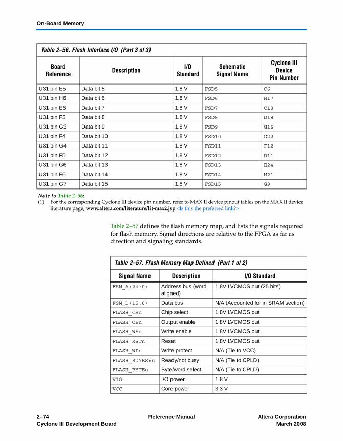
On-Board Memory
Table 2–57 defines the flash memory map, and lists the signals required for flash memory. Signal directions are relative to the FPGA as far as direction and signaling standards.
U31 pin E5 Data bit 5 1.8 V FSD5 C6
U31 pin H6 Data bit 6 1.8 V FSD6 H17
U31 pin E6 Data bit 7 1.8 V FSD7 C18
U31 pin F3 Data bit 8 1.8 V FSD8 D18
U31 pin G3 Data bit 9 1.8 V FSD9 G16
U31 pin F4 Data bit 10 1.8 V FSD10 G22
U31 pin G4 Data bit 11 1.8 V FSD11 F12
U31 pin F5 Data bit 12 1.8 V FSD12 D11
U31 pin G6 Data bit 13 1.8 V FSD13 E24
U31 pin F6 Data bit 14 1.8 V FSD14 H21
U31 pin G7 Data bit 15 1.8 V FSD15 G9
Note to Table 2–56:(1) For the corresponding Cyclone III device pin number, refer to MAX II device pinout tables on the MAX II device
literature page, www.altera.com/literature/lit-max2.jsp.<Is this the preferred link?>
Table 2–56. Flash Interface I/O (Part 3 of 3)
BoardReference Description I/O
StandardSchematic
Signal Name
Cyclone III Device
Pin Number
Table 2–57. Flash Memory Map Defined (Part 1 of 2)
Signal Name Description I/O Standard
FSM_A(24:0) Address bus (word aligned)
1.8V LVCMOS out (25 bits)
FSM_D(15:0) Data bus N/A (Accounted for in SRAM section)
FLASH_CSn Chip select 1.8V LVCMOS out
FLASH_OEn Output enable 1.8V LVCMOS out
FLASH_WEn Write enable 1.8V LVCMOS out
FLASH_RSTn Reset 1.8V LVCMOS out
FLASH_WPn Write protect N/A (Tie to VCC)
FLASH_RDYBSYn Ready/not busy N/A (Tie to CPLD)
FLASH_BYTEn Byte/word select N/A (Tie to CPLD)
VIO I/O power 1.8 V
VCC Core power 3.3 V
2–74 Reference Manual Altera CorporationCyclone III Development Board March 2008
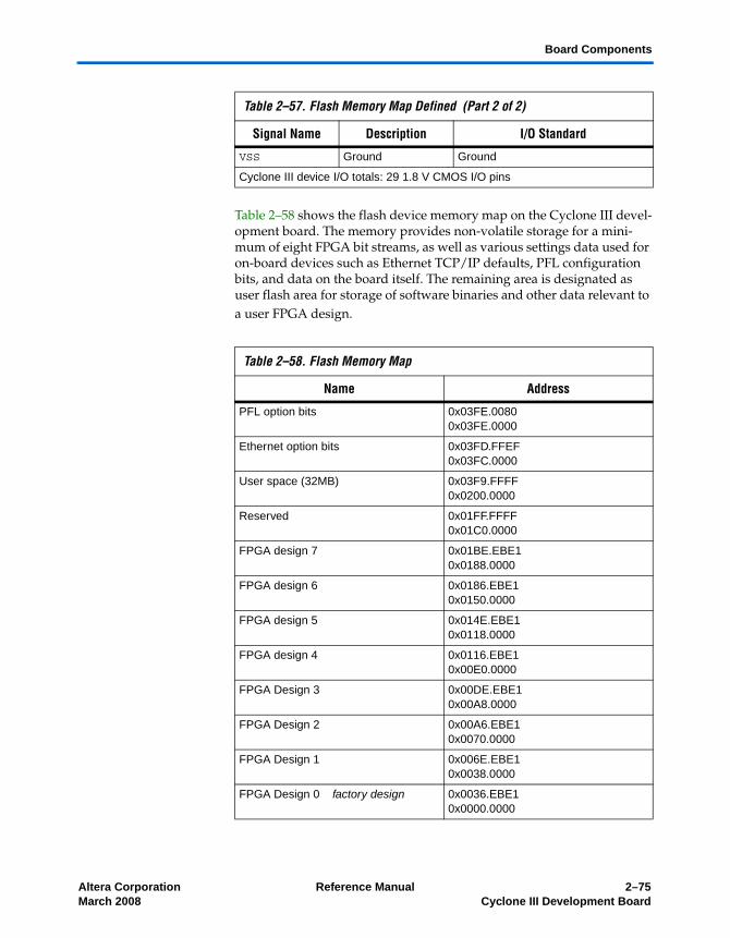
Board Components
Table 2–58 shows the flash device memory map on the Cyclone III devel-opment board. The memory provides non-volatile storage for a mini-mum of eight FPGA bit streams, as well as various settings data used for on-board devices such as Ethernet TCP/IP defaults, PFL configuration bits, and data on the board itself. The remaining area is designated as user flash area for storage of software binaries and other data relevant to a user FPGA design.
VSS Ground Ground
Cyclone III device I/O totals: 29 1.8 V CMOS I/O pins
Table 2–58. Flash Memory Map
Name Address
PFL option bits 0x03FE.00800x03FE.0000
Ethernet option bits 0x03FD.FFEF0x03FC.0000
User space (32MB) 0x03F9.FFFF0x0200.0000
Reserved 0x01FF.FFFF0x01C0.0000
FPGA design 7 0x01BE.EBE10x0188.0000
FPGA design 6 0x0186.EBE10x0150.0000
FPGA design 5 0x014E.EBE10x0118.0000
FPGA design 4 0x0116.EBE10x00E0.0000
FPGA Design 3 0x00DE.EBE10x00A8.0000
FPGA Design 2 0x00A6.EBE10x0070.0000
FPGA Design 1 0x006E.EBE10x0038.0000
FPGA Design 0 factory design 0x0036.EBE10x0000.0000
Table 2–57. Flash Memory Map Defined (Part 2 of 2)
Signal Name Description I/O Standard
Altera Corporation Reference Manual 2–75March 2008 Cyclone III Development Board
On-Board Memory
f For information on the flash array command set and sequencing for register access, or any other data regarding the Spansion device, visit www. spansion.com.
Tables 2–59 and 2–60 are from the Spansion flash device data sheet. The tables show the top and bottom sections of the flash sector map, along with the manufacturer’s sector address map.
Table 2–61 lists Spansion flash board reference and manufacturing information.
Table 2–59. Flash Sector Map - Bottom
Sector A24-A16
Sector Size
(Kybtes)Kwords
8-BitAddress Range (In
hexadecimal)
16-bitAddress Range (In
hexadecimal)
SA0 0 0 0 0 0 0 0 0 0 128/64 0000000–001FFFF 0000000–000FFFF
SA1 0 0 0 0 0 0 0 0 1 128/64 0020000–003FFFF 0010000–001FFFF
SA2 0 0 0 0 0 0 0 1 0 128/64 0040000–005FFFF 0020000–002FFFF
SA3 0 0 0 0 0 0 0 1 1 128/64 0060000–007FFFF 0030000–003FFFF
SA4 0 0 0 0 0 0 1 0 0 128/64 0080000–009FFFF 0040000–004FFFF
SA5 0 0 0 0 0 0 1 0 1 128/64 00A0000–00BFFFF 0050000–005FFFF
Table 2–60. Flash Sector Map - Top
Sector A24-A16
Sector Size
(Kybtes)Kwords
8-BitAddress Range (In
hexadecimal)
16-bitAddress Range (In
hexadecimal)
SA508 1 1 1 1 1 1 1 0 0 128/64 3F80000–3F9FFFF 1FC0000–1FCFFFF
SA509 1 1 1 1 1 1 1 0 1 128/64 3FA0000–3FBFFFF 1FD0000–1FDFFFF
SA510 1 1 1 1 1 1 1 1 0 128/64 3FC0000–3FDFFFF 1FE0000–1FEFFFF
SA511 1 1 1 1 1 1 1 1 1 128/64 3FE0000–3FFFFFF 1FF0000–1FFFFFF
Table 2–61. Spansion Flash Manufacturing Information
Board Reference Description Manufacturer Manufacturer Part
NumberManufacturer
Web Site
U31 64 MB of flash memory
Spansion LLC S29GL512N11FFIV1 www.spansion.com
2–76 Reference Manual Altera CorporationCyclone III Development Board March 2008
Board Components
Power Supply The board’s power is provided through an IBM laptop style DC power input. The input voltage must be in the range of 14 V to 20 V. The DC voltage is then stepped down to the various power rails used by the components on the board and installed into the HSMC connectors.
Figure 2–17 shows the power distribution system, which uses current power rails as described in “POWER SELECT Rotary Switch” on page 2–25. Regulator inefficiencies and sharing are reflected in the currents shown.
Altera Corporation Reference Manual 2–77March 2008 Cyclone III Development Board
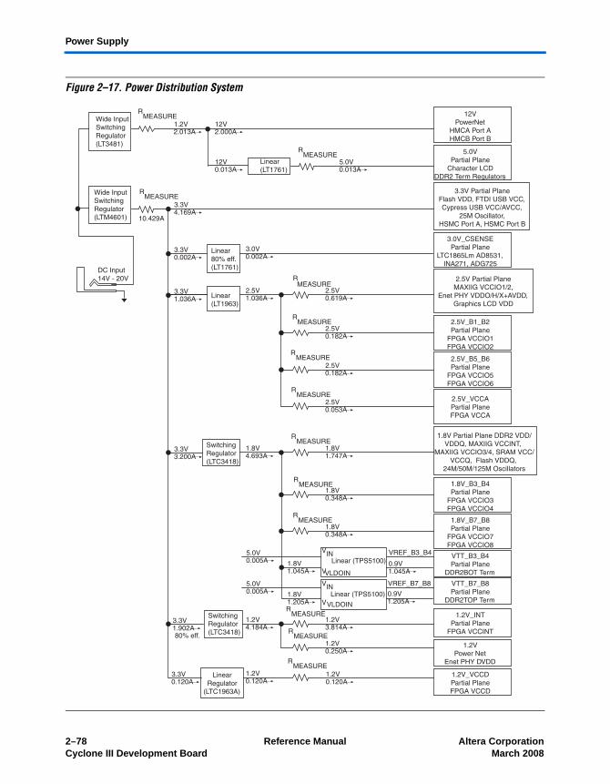
Power Supply
2–78 Reference Manual Altera Corporation
Figure 2–17. Power Distribution System
Cyclone III Development Board March 2008
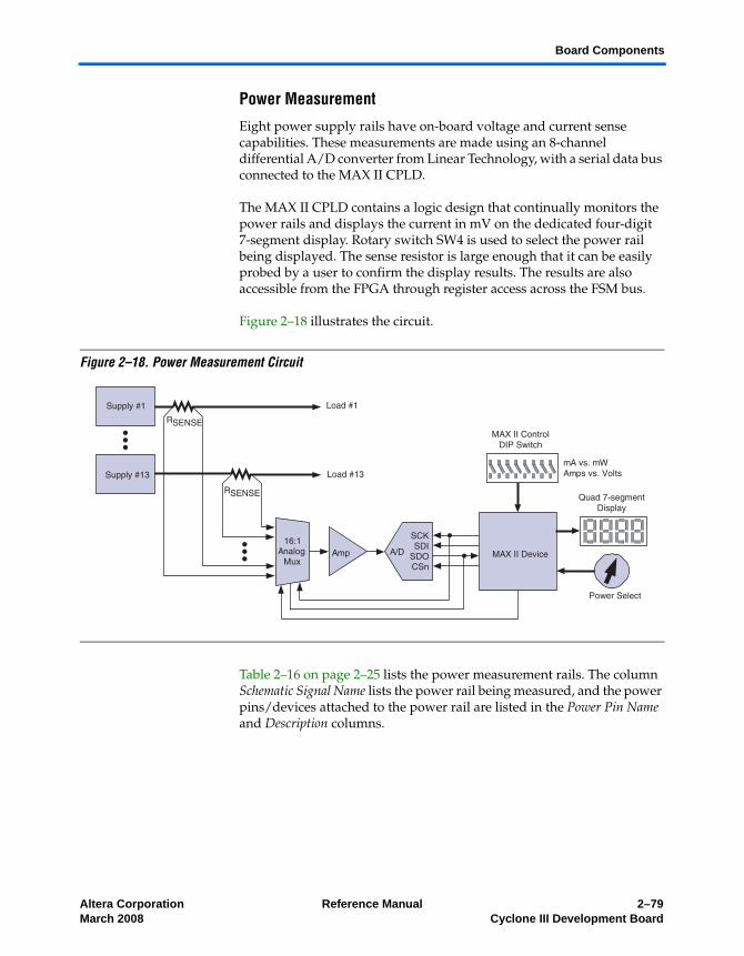
Board Components
Power Measurement
Eight power supply rails have on-board voltage and current sense capabilities. These measurements are made using an 8-channel differential A/D converter from Linear Technology, with a serial data bus connected to the MAX II CPLD.
The MAX II CPLD contains a logic design that continually monitors the power rails and displays the current in mV on the dedicated four-digit 7-segment display. Rotary switch SW4 is used to select the power rail being displayed. The sense resistor is large enough that it can be easily probed by a user to confirm the display results. The results are also accessible from the FPGA through register access across the FSM bus.
Figure 2–18 illustrates the circuit.
Figure 2–18. Power Measurement Circuit
Table 2–16 on page 2–25 lists the power measurement rails. The column Schematic Signal Name lists the power rail being measured, and the power pins/devices attached to the power rail are listed in the Power Pin Name and Description columns.
Altera Corporation Reference Manual 2–79March 2008 Cyclone III Development Board
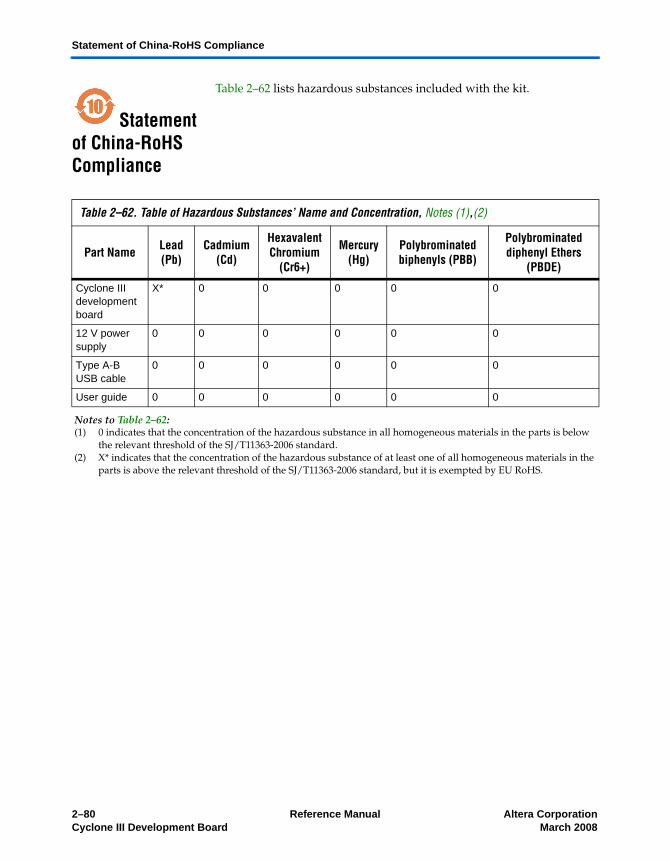
Statement of China-RoHS Compliance
Statement of China-RoHS Compliance
Table 2–62 lists hazardous substances included with the kit.
Table 2–62. Table of Hazardous Substances’ Name and Concentration, Notes (1),(2)
Part Name Lead (Pb)
Cadmium (Cd)
Hexavalent Chromium
(Cr6+)
Mercury (Hg)
Polybrominatedbiphenyls (PBB)
Polybrominateddiphenyl Ethers
(PBDE)
Cyclone III development board
X* 0 0 0 0 0
12 V power supply
0 0 0 0 0 0
Type A-B USB cable
0 0 0 0 0 0
User guide 0 0 0 0 0 0
Notes to Table 2–62:(1) 0 indicates that the concentration of the hazardous substance in all homogeneous materials in the parts is below
the relevant threshold of the SJ/T11363-2006 standard.(2) X* indicates that the concentration of the hazardous substance of at least one of all homogeneous materials in the
parts is above the relevant threshold of the SJ/T11363-2006 standard, but it is exempted by EU RoHS.
2–80 Reference Manual Altera CorporationCyclone III Development Board March 2008