Basics of Measuring the Dielectric Properties of Materials
32
Agilent Basics of Measuring the Dielectric Properties of Materials Application Note
-
Upload
jrpegoraro -
Category
Documents
-
view
76 -
download
10
Transcript of Basics of Measuring the Dielectric Properties of Materials

AgilentBasics of Measuring the Dielectric Properties of Materials
Application Note
Contents
2
Introduction ..............................................................................................3
Dielectric theory .....................................................................................4
Dielectric Constant ............................................................................4
Permeability........................................................................................7
Electromagnetic propagation .................................................................8
Dielectric mechanisms ........................................................................10
Orientation (dipolar) polarization ................................................11
Electronic and atomic polarization ..............................................11
Relaxation time ................................................................................12
Debye Relation .................................................................................12
Cole-Cole diagram............................................................................13
Ionic conductivity ............................................................................13
Interfacial or space charge polarization..................................... 14
Measurement Systems .........................................................................15
Network analyzers ..........................................................................15
Impedance analyzers and LCR meters .........................................16
Fixtures .............................................................................................16
Software ............................................................................................16
Measurement techniques .....................................................................17
Coaxial probe ...................................................................................17
Transmission line ............................................................................20
Free space .........................................................................................23
Resonant cavity ...............................................................................25
Parallel plate ...................................................................................27
Comparison of methods ........................................................................28
References..............................................................................................30
Web Resources ......................................................................................32
Introduction Every material has a unique set of electrical characteristics that are dependent on its dielectric properties. Accurate measurements of theseproperties can provide scientists and engineers with valuable information toproperly incorporate the material into its intended application for moresolid designs or to monitor a manufacturing process for improved qualitycontrol.
A dielectric materials measurement can provide critical design parameterinformation for many electronics applications. For example, the loss of acable insulator, the impedance of a substrate, or the frequency of a dielectricresonator can be related to its dielectric properties. The information is alsouseful for improving ferrite, absorber, and packaging designs. More recentapplications in the area of industrial microwave processing of food, rubber,plastic and ceramics have also been found to benefit from knowledge ofdielectric properties.
Agilent Technologies Inc. offers a variety of instruments, fixtures, and software to measure the dielectric properties of materials. Agilent measure-ment instruments, such as network analyzers, LCR meters, and impedanceanalyzers range in frequency up to 325 GHz. Fixtures to hold the materialunder test (MUT) are available that are based on coaxial probe,coaxial/waveguide transmission line techniques, and parallel plate.
3
Dielectric Theory The dielectric properties that will be discussed here are permittivity andpermeability. Resistivity is another material property which will not be discussed here. Information about resistivity and its measurement can befound in the Agilent Application Note 1369-11. It is important to note thatpermittivity and permeability are not constant. They can change with frequency, temperature, orientation, mixture, pressure, and molecular structure of the material.
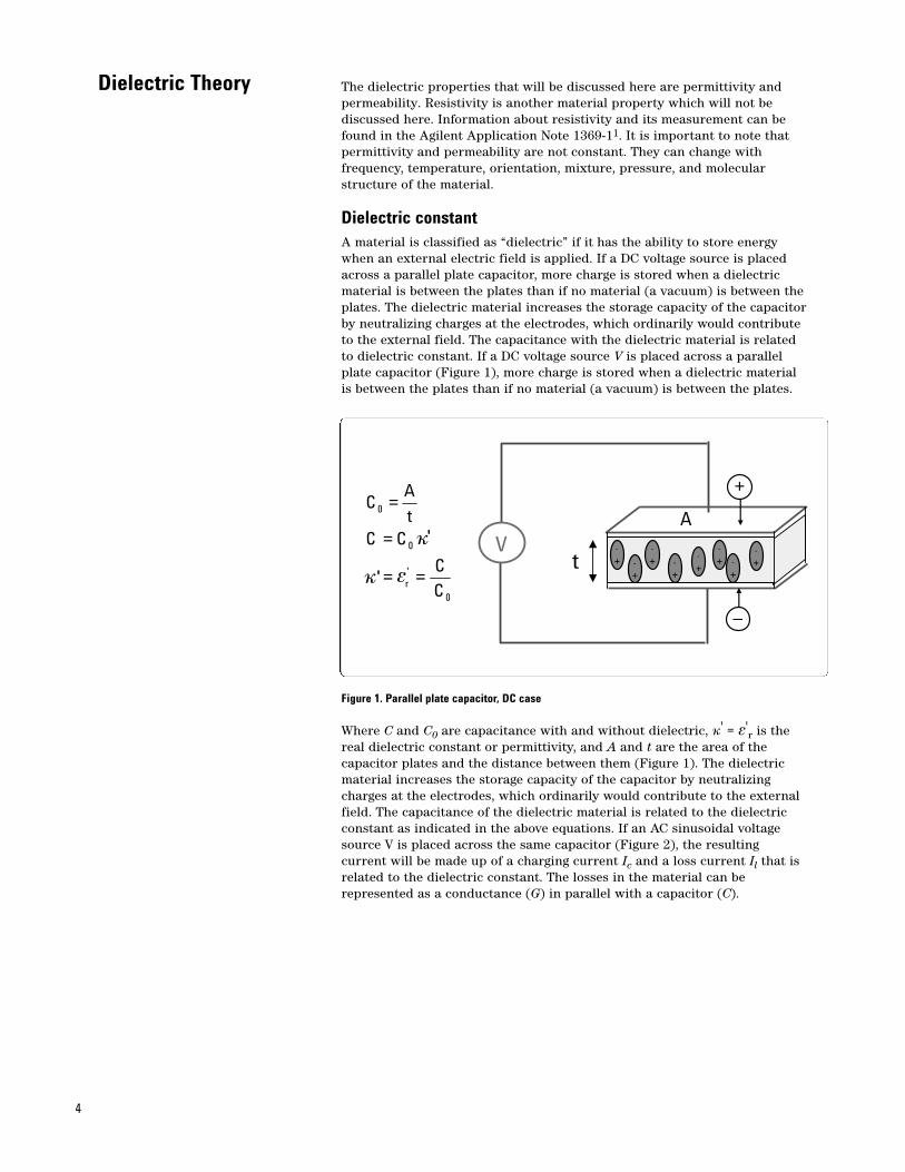
Dielectric constantA material is classified as “dielectric” if it has the ability to store energywhen an external electric field is applied. If a DC voltage source is placedacross a parallel plate capacitor, more charge is stored when a dielectricmaterial is between the plates than if no material (a vacuum) is between theplates. The dielectric material increases the storage capacity of the capacitorby neutralizing charges at the electrodes, which ordinarily would contributeto the external field. The capacitance with the dielectric material is relatedto dielectric constant. If a DC voltage source V is placed across a parallelplate capacitor (Figure 1), more charge is stored when a dielectric materialis between the plates than if no material (a vacuum) is between the plates.
Figure 1. Parallel plate capacitor, DC case
Where C and C0 are capacitance with and without dielectric, k' = e'r is the
real dielectric constant or permittivity, and A and t are the area of thecapacitor plates and the distance between them (Figure 1). The dielectricmaterial increases the storage capacity of the capacitor by neutralizingcharges at the electrodes, which ordinarily would contribute to the externalfield. The capacitance of the dielectric material is related to the dielectricconstant as indicated in the above equations. If an AC sinusoidal voltagesource V is placed across the same capacitor (Figure 2), the resulting current will be made up of a charging current Ic and a loss current Il that isrelated to the dielectric constant. The losses in the material can be represented as a conductance (G) in parallel with a capacitor (C).
4
t
A
-+
-+
-+ -
+
-+
-+
-+-
+
+
–
V
0
'
0
0
k'
'
C
C
CCt
AC
r ==
=
=
k
e
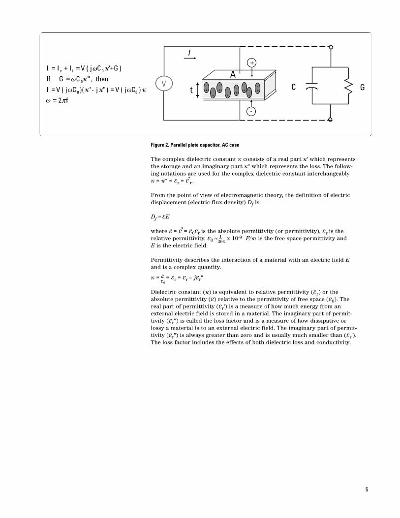
Figure 2. Parallel plate capacitor, AC case
The complex dielectric constant k consists of a real part k' which representsthe storage and an imaginary part k'' which represents the loss. The follow-ing notations are used for the complex dielectric constant interchangeably k = k* = er = e*r .
From the point of view of electromagnetic theory, the definition of electricdisplacement (electric flux density) Df is:
Df = eE
where e = e* = e0er is the absolute permittivity (or permittivity), er is the relative permittivity, e0 ≈ 1
36π x 10-9 F/m is the free space permittivity and E is the electric field.
Permittivity describes the interaction of a material with an electric field Eand is a complex quantity.
k = ee0 = er = er – jer''
Dielectric constant (k) is equivalent to relative permittivity (er) or theabsolute permittivity (e) relative to the permittivity of free space (e0). Thereal part of permittivity (er') is a measure of how much energy from anexternal electric field is stored in a material. The imaginary part of permit-tivity (er'') is called the loss factor and is a measure of how dissipative orlossy a material is to an external electric field. The imaginary part of permit-tivity (er") is always greater than zero and is usually much smaller than (er').The loss factor includes the effects of both dielectric loss and conductivity.
5
C Gt
A
-+
-+
-+ -
+
-+
-+
-+-
+
+
-
V
I
f
CjVjCjVI
thenCGIf
GCjVIII lc
π2
)()"')((
,"
)'(
00
0
0
=
==
=
+=+= k
kk
k
k
w
w
w w
w
-

When complex permittivity is drawn as a simple vector diagram (Figure 3),the real and imaginary components are 90° out of phase. The vector sumforms an angle d with the real axis (er'). The relative “lossiness” of a material isthe ratio of the energy lost to the energy stored.
Figure 3. Loss tangent vector diagram
The loss tangent or tan d is defined as the ratio of the imaginary part of thedielectric constant to the real part. D denotes dissipation factor and Q isquality factor. The loss tangent tan d is called tan delta, tangent loss or dissipation factor. Sometimes the term “quality factor or Q-factor” is usedwith respect to an electronic microwave material, which is the reciprocal of the loss tangent. For very low loss materials, since tan d ≈ d, the loss tangent can be expressed in angle units, milliradians or microradians.
6
r
'r
''re
e
eEnergy Stored per Cycle
Energy Lost per Cycle
QD
r
r
=
===1
tan'
"ee
d
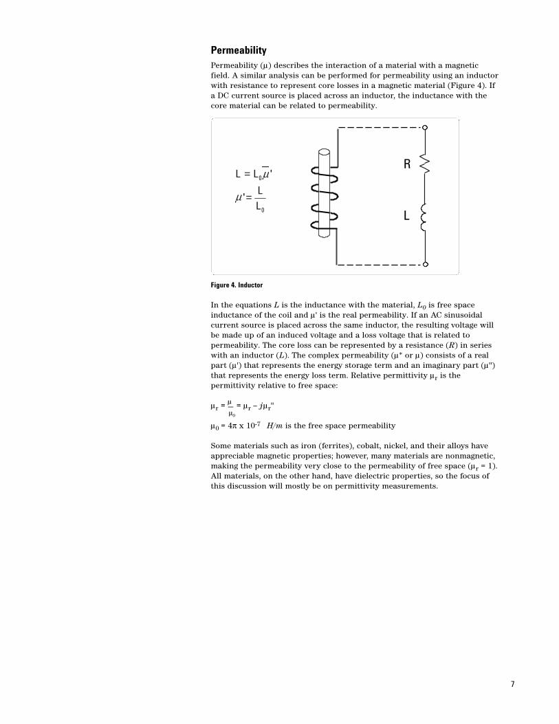
PermeabilityPermeability (µ) describes the interaction of a material with a magneticfield. A similar analysis can be performed for permeability using an inductorwith resistance to represent core losses in a magnetic material (Figure 4). Ifa DC current source is placed across an inductor, the inductance with thecore material can be related to permeability.
Figure 4. Inductor
In the equations L is the inductance with the material, L0 is free spaceinductance of the coil and µ' is the real permeability. If an AC sinusoidal current source is placed across the same inductor, the resulting voltage willbe made up of an induced voltage and a loss voltage that is related to permeability. The core loss can be represented by a resistance (R) in serieswith an inductor (L). The complex permeability (µ* or µ) consists of a realpart (µ') that represents the energy storage term and an imaginary part (µ'')that represents the energy loss term. Relative permittivity µr is the permittivity relative to free space:
µr = µ—µ0
= µr – jµr''
µ0 = 4π x 10-7 H/m is the free space permeability
Some materials such as iron (ferrites), cobalt, nickel, and their alloys haveappreciable magnetic properties; however, many materials are nonmagnetic,making the permeability very close to the permeability of free space (µr = 1).All materials, on the other hand, have dielectric properties, so the focus ofthis discussion will mostly be on permittivity measurements.
7
R
L0
0
'
'
L
L
LL
=
= µ
µ
Electromagnetic Wave Propagation
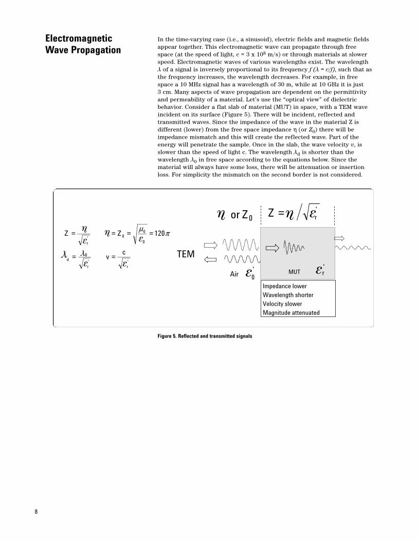
In the time-varying case (i.e., a sinusoid), electric fields and magnetic fieldsappear together. This electromagnetic wave can propagate through freespace (at the speed of light, c = 3 x 10⁸ m/s) or through materials at slowerspeed. Electromagnetic waves of various wavelengths exist. The wavelengthl of a signal is inversely proportional to its frequency f (l = c/f), such that asthe frequency increases, the wavelength decreases. For example, in freespace a 10 MHz signal has a wavelength of 30 m, while at 10 GHz it is just 3 cm. Many aspects of wave propagation are dependent on the permittivityand permeability of a material. Let’s use the “optical view” of dielectricbehavior. Consider a flat slab of material (MUT) in space, with a TEM waveincident on its surface (Figure 5). There will be incident, reflected and transmitted waves. Since the impedance of the wave in the material Z is different (lower) from the free space impedance η (or Z0) there will beimpedance mismatch and this will create the reflected wave. Part of theenergy will penetrate the sample. Once in the slab, the wave velocity v, isslower than the speed of light c. The wavelength ld is shorter than the wavelength l0 in free space according to the equations below. Since thematerial will always have some loss, there will be attenuation or insertionloss. For simplicity the mismatch on the second border is not considered.
Figure 5. Reflected and transmitted signals
8
MUT
Impedance lowerWavelength shorterVelocity slowerMagnitude attenuated
TEM
or Z 0'rZ =
'rAir
'0
e
e e
h h
''
0
0
00'
120
rr
d
r
cv
ZZ πµ
==
====h h
llee
e e

Figure 6 depicts the relation between the dielectric constant of the MaterialUnder Test (MUT) and the reflection coefficient |G| for an infinitely longsample (no reflection from the back of the sample is considered). For smallvalues of the dielectric constant (approximately less than 20), there is a lotof change of the reflection coefficient for a small change of the dielectricconstant. In this range dielectric constant measurement using the reflectioncoefficient will be more sensitive and hence precise. Conversely, for highdielectric constants (for example between 70 and 90) there will be littlechange of the reflection coefficient and the measurement will have moreuncertainty.
Figure 6. Reflection coefficient versus dielectric constant
9
10 20 30 40 50 60 70 80 90 1000
0.1
0.2
0.3
0.4
0.5
0.6
0.7
0.8
0.9
1
Dielectric constant
Ref
lect
ion
coef
ficie
nt
G|
|
're
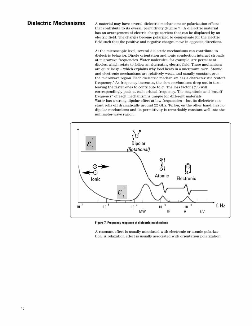
Dielectric Mechanisms A material may have several dielectric mechanisms or polarization effectsthat contribute to its overall permittivity (Figure 7). A dielectric material has an arrangement of electric charge carriers that can be displaced by anelectric field. The charges become polarized to compensate for the electricfield such that the positive and negative charges move in opposite directions.
At the microscopic level, several dielectric mechanisms can contribute todielectric behavior. Dipole orientation and ionic conduction interact stronglyat microwave frequencies. Water molecules, for example, are permanentdipoles, which rotate to follow an alternating electric field. These mechanismsare quite lossy – which explains why food heats in a microwave oven. Atomicand electronic mechanisms are relatively weak, and usually constant overthe microwave region. Each dielectric mechanism has a characteristic “cutofffrequency.” As frequency increases, the slow mechanisms drop out in turn,leaving the faster ones to contribute to e'. The loss factor (er'') will correspondingly peak at each critical frequency. The magnitude and “cutofffrequency” of each mechanism is unique for different materials.Water has a strong dipolar effect at low frequencies – but its dielectric con-stant rolls off dramatically around 22 GHz. Teflon, on the other hand, has nodipolar mechanisms and its permittivity is remarkably constant well into themillimeter-wave region.
Figure 7. Frequency response of dielectric mechanisms
A resonant effect is usually associated with electronic or atomic polariza-tion. A relaxation effect is usually associated with orientation polarization.
10
Dipolar(Rotational)
Atomic Electronic
103
106
109
1012
1015 f, Hz
VIRMW UV
+
-
Ionic
'r
''r
+
+
--
e
e
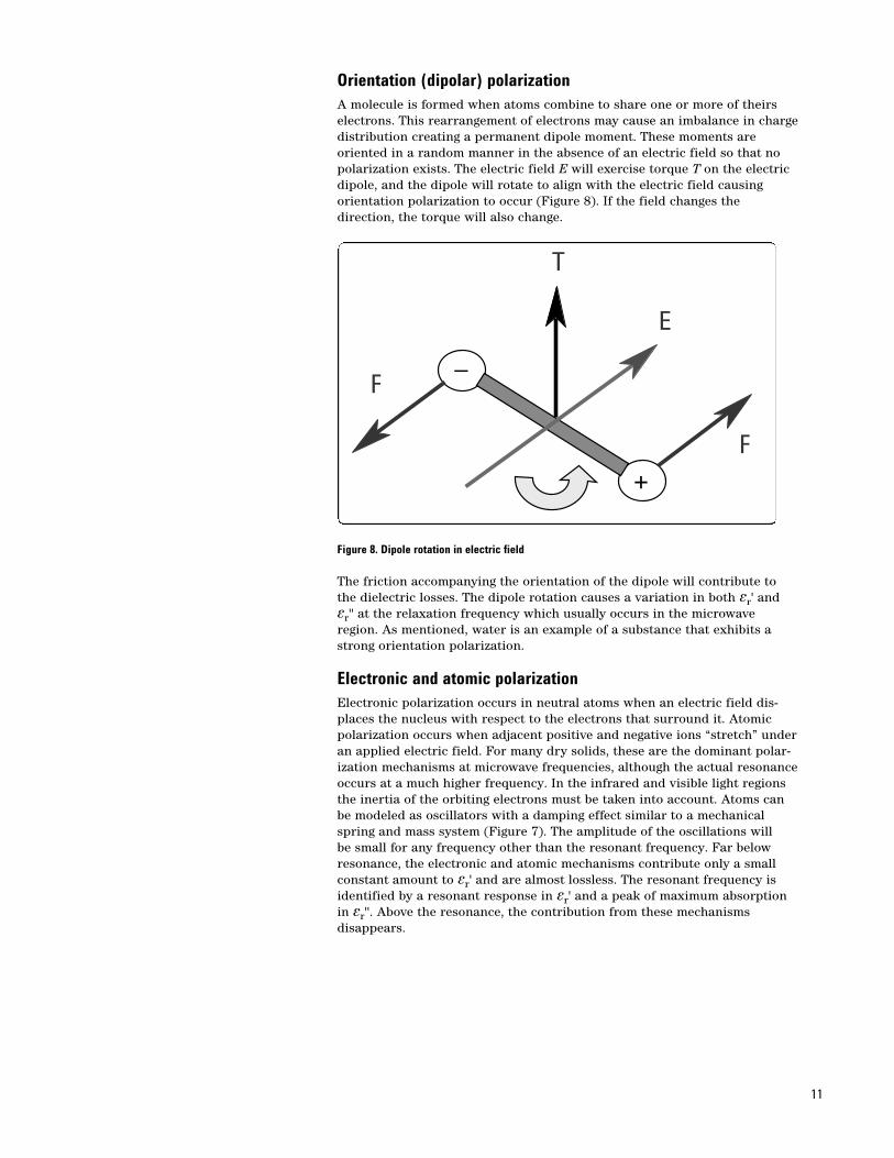
Orientation (dipolar) polarizationA molecule is formed when atoms combine to share one or more of theirselectrons. This rearrangement of electrons may cause an imbalance in chargedistribution creating a permanent dipole moment. These moments are oriented in a random manner in the absence of an electric field so that nopolarization exists. The electric field E will exercise torque T on the electricdipole, and the dipole will rotate to align with the electric field causing orientation polarization to occur (Figure 8). If the field changes the direction, the torque will also change.
Figure 8. Dipole rotation in electric field
The friction accompanying the orientation of the dipole will contribute tothe dielectric losses. The dipole rotation causes a variation in both er' ander'' at the relaxation frequency which usually occurs in the microwaveregion. As mentioned, water is an example of a substance that exhibits astrong orientation polarization.
Electronic and atomic polarizationElectronic polarization occurs in neutral atoms when an electric field dis-places the nucleus with respect to the electrons that surround it. Atomicpolarization occurs when adjacent positive and negative ions “stretch” underan applied electric field. For many dry solids, these are the dominant polar-ization mechanisms at microwave frequencies, although the actual resonanceoccurs at a much higher frequency. In the infrared and visible light regionsthe inertia of the orbiting electrons must be taken into account. Atoms canbe modeled as oscillators with a damping effect similar to a mechanicalspring and mass system (Figure 7). The amplitude of the oscillations will be small for any frequency other than the resonant frequency. Far below resonance, the electronic and atomic mechanisms contribute only a smallconstant amount to er' and are almost lossless. The resonant frequency isidentified by a resonant response in er' and a peak of maximum absorptionin er''. Above the resonance, the contribution from these mechanisms disappears.
11
+
–
F
F
T
E
Relaxation timeRelaxation time τ is a measure of the mobility of the molecules (dipoles) thatexist in a material. It is the time required for a displaced system aligned inan electric field to return to 1/e of its random equilibrium value (or the timerequired for dipoles to become oriented in an electric field). Liquid and solidmaterials have molecules that are in a condensed state with limited freedomto move when an electric field is applied. Constant collisions cause internalfriction so that the molecules turn slowly and exponentially approach thefinal state of orientation polarization with relaxation time constant τ. Whenthe field is switched off, the sequence is reversed and random distribution isrestored with the same time constant.
The relaxation frequency fc is inversely related to relaxation time:
At frequencies below relaxation the alternating electric field is slow enoughthat the dipoles are able to keep pace with the field variations. Because thepolarization is able to develop fully, the loss (er'') is directly proportional tothe frequency (Figure 9). As the frequency increases, er'' continues toincrease but the storage (er') begins to decrease due to the phase lagbetween the dipole alignment and the electric field. Above the relaxation frequency both er'' and er' drop off as the electric field is too fast to influence the dipole rotation and the orientation polarization disappears.
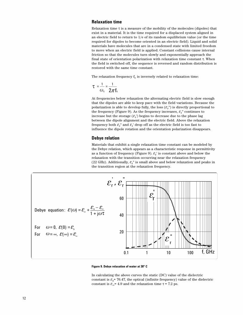
Debye relationMaterials that exhibit a single relaxation time constant can be modeled bythe Debye relation, which appears as a characteristic response in permittivityas a function of frequency (Figure 9). er' is constant above and below therelaxation with the transition occurring near the relaxation frequency (22 GHz). Additionally, er'' is small above and below relaxation and peaks inthe transition region at the relaxation frequency.
Figure 9. Debye relaxation of water at 30º C
In calculating the above curves the static (DC) value of the dielectric constant is es= 76.47, the optical (infinite frequency) value of the dielectricconstant is e∞= 4.9 and the relaxation time τ = 7.2 ps.
12
cc fπ211
==w
τ
0.1 1 10 100
20
40
60'r
"r
f, GHz
''' , rre ee
e∞
∞∞
=∞∞=
==
++=
)(,
)0(,0
1)( :equation Debye
For
For
–
j
s
sww
ww
e e e
ee
ee
eτ
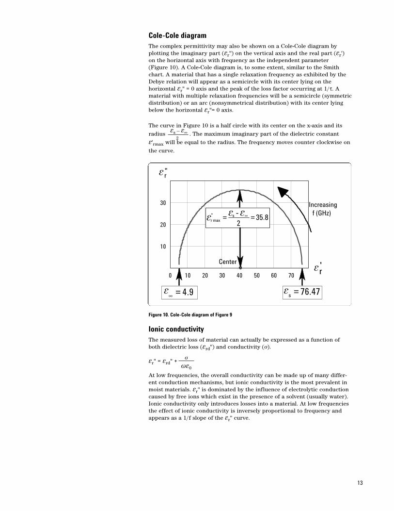
Cole-Cole diagramThe complex permittivity may also be shown on a Cole-Cole diagram by plotting the imaginary part (er'') on the vertical axis and the real part (er')on the horizontal axis with frequency as the independent parameter (Figure 10). A Cole-Cole diagram is, to some extent, similar to the Smithchart. A material that has a single relaxation frequency as exhibited by theDebye relation will appear as a semicircle with its center lying on the horizontal er'' = 0 axis and the peak of the loss factor occurring at 1/τ. Amaterial with multiple relaxation frequencies will be a semicircle (symmetricdistribution) or an arc (nonsymmetrical distribution) with its center lyingbelow the horizontal er''= 0 axis.
The curve in Figure 10 is a half circle with its center on the x-axis and its
radius . The maximum imaginary part of the dielectric constant
e'rmax will be equal to the radius. The frequency moves counter clockwise on
the curve.
Figure 10. Cole-Cole diagram of Figure 9
Ionic conductivityThe measured loss of material can actually be expressed as a function ofboth dielectric loss (erd'') and conductivity (s).
er'' = erd'' +
At low frequencies, the overall conductivity can be made up of many differ-ent conduction mechanisms, but ionic conductivity is the most prevalent inmoist materials. er'' is dominated by the influence of electrolytic conductioncaused by free ions which exist in the presence of a solvent (usually water).Ionic conductivity only introduces losses into a material. At low frequenciesthe effect of ionic conductivity is inversely proportional to frequency andappears as a 1/f slope of the er'' curve.
13
0 10 20 30 40 50 60 70
10
20
30
"r
'r
9.4=∞ 47.76=s
Increasingf (GHz)
8.352
"max == ∞s
r
Center
e
e
e e
e ee -
es — e∞2
s
we0
Interfacial or space charge polarizationElectronic, atomic, and orientation polarization occur when charges arelocally bound in atoms, molecules, or structures of solids or liquids. Chargecarriers also exist that can migrate over a distance through the materialwhen a low frequency electric field is applied. Interfacial or space chargepolarization occurs when the motion of these migrating charges is impeded.The charges can become trapped within the interfaces of a material. Motionmay also be impeded when charges cannot be freely discharged or replacedat the electrodes. The field distortion caused by the accumulation of thesecharges increases the overall capacitance of a material which appears as anincrease in er'.
Mixtures of materials with electrically conducting regions that are not incontact with each other (separated by non-conducting regions) exhibit theMaxwell-Wagner effect at low frequencies. If the charge layers are thin and much smaller than the particle dimensions, the charge responds independently of the charge on nearby particles. At low frequencies thecharges have time to accumulate at the borders of the conducting regionscausing er' to increase. At higher frequencies the charges do not have time toaccumulate and polarization does not occur since the charge displacement issmall compared to the dimensions of the conducting region. As the frequencyincreases, er' decreases and the losses exhibit the same 1/f slope as normalionic conductivity.
Many other dielectric mechanisms can occur in this low frequency regioncausing a significant variation in permittivity. For example, colloidal suspension occurs if the charge layer is on the same order of thickness orlarger than the particle dimensions. The Maxwell-Wagner effect is no longerapplicable since the response is now affected by the charge distribution ofadjacent particles.
14
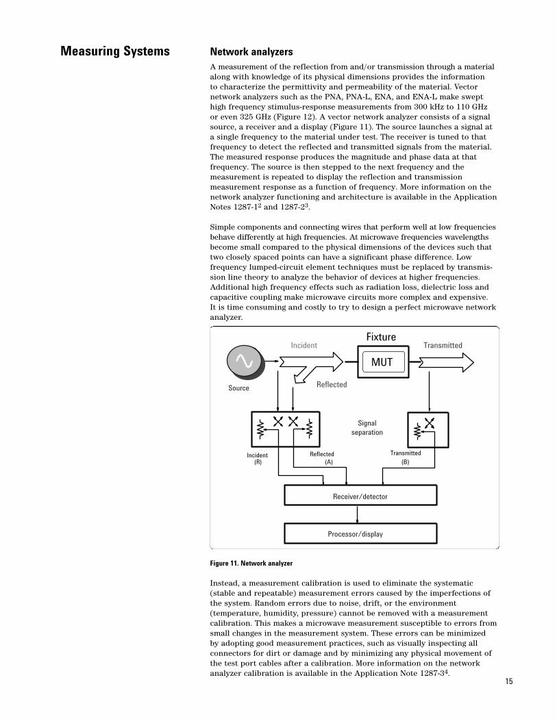
Measuring Systems Network analyzersA measurement of the reflection from and/or transmission through a materialalong with knowledge of its physical dimensions provides the information to characterize the permittivity and permeability of the material. Vector network analyzers such as the PNA, PNA-L, ENA, and ENA-L make swepthigh frequency stimulus-response measurements from 300 kHz to 110 GHzor even 325 GHz (Figure 12). A vector network analyzer consists of a signalsource, a receiver and a display (Figure 11). The source launches a signal ata single frequency to the material under test. The receiver is tuned to thatfrequency to detect the reflected and transmitted signals from the material.The measured response produces the magnitude and phase data at that frequency. The source is then stepped to the next frequency and the measurement is repeated to display the reflection and transmission measurement response as a function of frequency. More information on thenetwork analyzer functioning and architecture is available in the ApplicationNotes 1287-12 and 1287-23.
Simple components and connecting wires that perform well at low frequenciesbehave differently at high frequencies. At microwave frequencies wavelengthsbecome small compared to the physical dimensions of the devices such thattwo closely spaced points can have a significant phase difference. Low frequency lumped-circuit element techniques must be replaced by transmis-sion line theory to analyze the behavior of devices at higher frequencies.Additional high frequency effects such as radiation loss, dielectric loss andcapacitive coupling make microwave circuits more complex and expensive. It is time consuming and costly to try to design a perfect microwave networkanalyzer.
Figure 11. Network analyzer
Instead, a measurement calibration is used to eliminate the systematic (stable and repeatable) measurement errors caused by the imperfections ofthe system. Random errors due to noise, drift, or the environment (temperature, humidity, pressure) cannot be removed with a measurementcalibration. This makes a microwave measurement susceptible to errors fromsmall changes in the measurement system. These errors can be minimized by adopting good measurement practices, such as visually inspecting all connectors for dirt or damage and by minimizing any physical movement ofthe test port cables after a calibration. More information on the networkanalyzer calibration is available in the Application Note 1287-34.
15
Receiver/detector
Processor/display
Reflected(A) (B)
Incident(R)
Signalseparation
Source
Incident
Reflected
Transmitted
Transmitted
MUT
Fixture
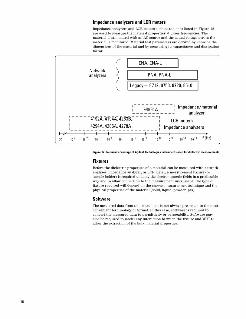
Impedance analyzers and LCR metersImpedance analyzers and LCR meters such as the ones listed in Figure 12are used to measure the material properties at lower frequencies. The material is stimulated with an AC source and the actual voltage across thematerial is monitored. Material test parameters are derived by knowing thedimensions of the material and by measuring its capacitance and dissipationfactor.
Figure 12. Frequency coverage of Agilent Technologies instruments used for dielectric measurements
FixturesBefore the dielectric properties of a material can be measured with networkanalyzer, impedance analyzer, or LCR meter, a measurement fixture (or sample holder) is required to apply the electromagnetic fields in a predictableway and to allow connection to the measurement instrument. The type offixture required will depend on the chosen measurement technique and thephysical properties of the material (solid, liquid, powder, gas).
SoftwareThe measured data from the instrument is not always presented in the mostconvenient terminology or format. In this case, software is required to convert the measured data to permittivity or permeability. Software mayalso be required to model any interaction between the fixture and MUT toallow the extraction of the bulk material properties.
16
10 10 10
4192A, 4194A, 4263B, LCR meters
Network
DC f (Hz)1 2 3 10 4 10 5 10 6 10 7 10 8 10 9 10 10 10 11
Impedance analyzers
analyzers
4294A, 4285A, 4278A
Legacy – 8712, 8753, 8720, 8510
ENA, ENA-L
E4991A Impedance/material analyzer
PNA, PNA-L
MeasurementTechniques
Coaxial probe
Method features• Broadband• Simple and convenient (non-destructive)• Limited er accuracy and tan d low loss resolution• Best for liquids or semi-solids
Material assumptions• “Semi-infinite” thickness• Non-magnetic• Isotropic and homogeneous• Flat surface• No air gaps
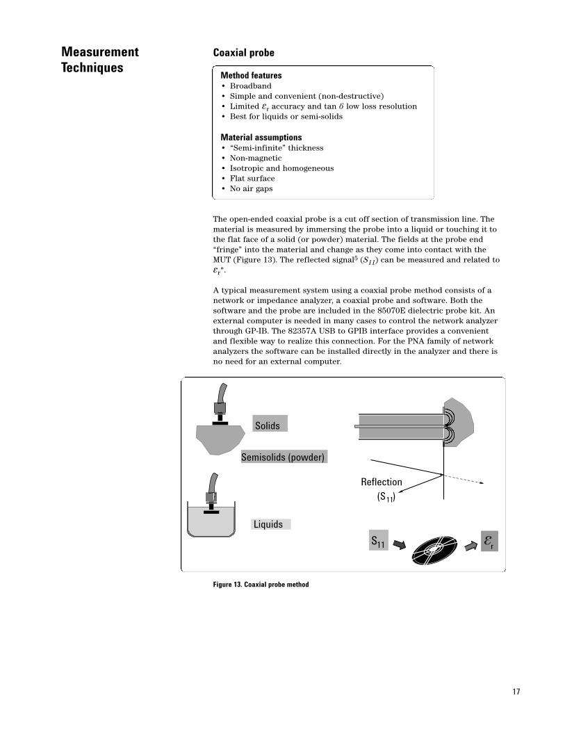
The open-ended coaxial probe is a cut off section of transmission line. Thematerial is measured by immersing the probe into a liquid or touching it tothe flat face of a solid (or powder) material. The fields at the probe end“fringe” into the material and change as they come into contact with theMUT (Figure 13). The reflected signal5 (S11) can be measured and related toer*.
A typical measurement system using a coaxial probe method consists of anetwork or impedance analyzer, a coaxial probe and software. Both the software and the probe are included in the 85070E dielectric probe kit. Anexternal computer is needed in many cases to control the network analyzerthrough GP-IB. The 82357A USB to GPIB interface provides a convenientand flexible way to realize this connection. For the PNA family of network analyzers the software can be installed directly in the analyzer and there isno need for an external computer.
Figure 13. Coaxial probe method
17
11
Solids
Liquids
Reflection(S )
11S r
Semisolids (powder)
e
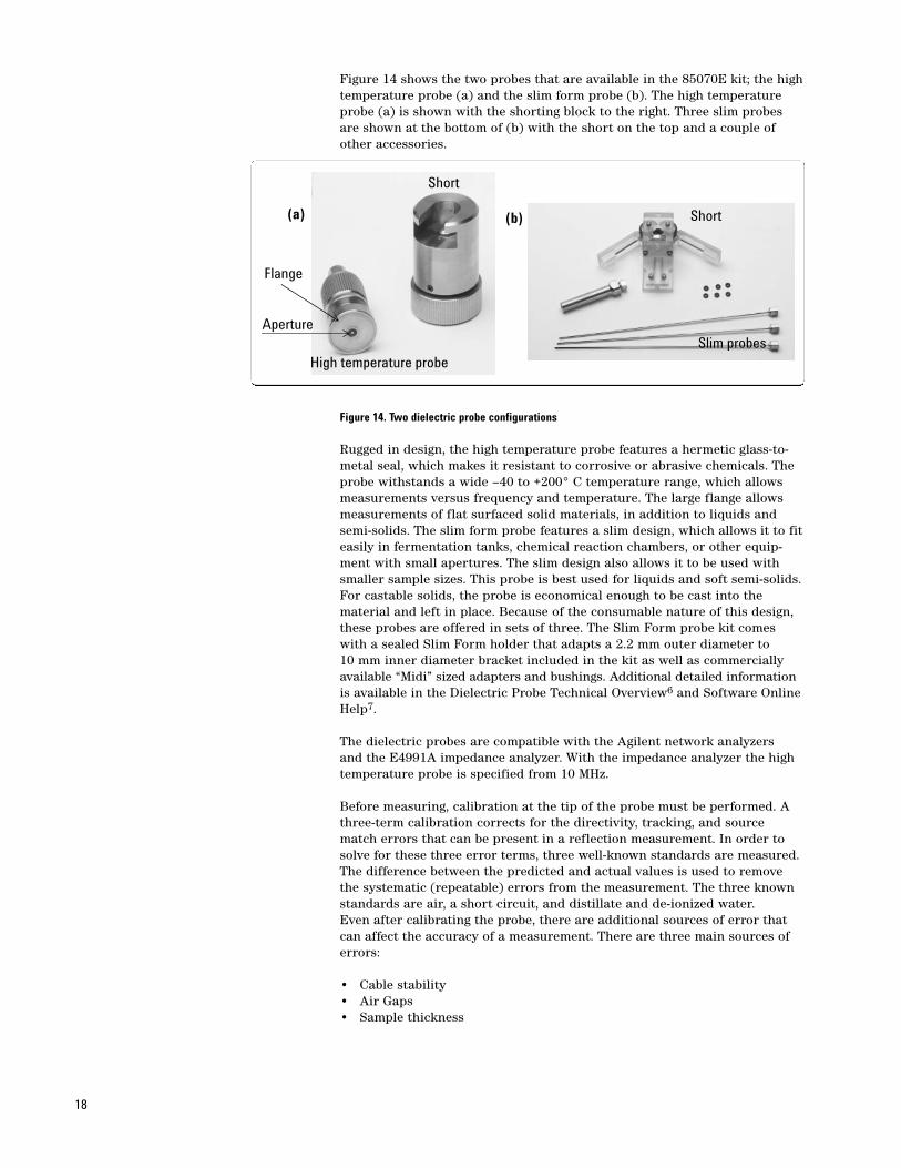
Figure 14 shows the two probes that are available in the 85070E kit; the hightemperature probe (a) and the slim form probe (b). The high temperatureprobe (a) is shown with the shorting block to the right. Three slim probesare shown at the bottom of (b) with the short on the top and a couple ofother accessories.
Figure 14. Two dielectric probe configurations
Rugged in design, the high temperature probe features a hermetic glass-to-metal seal, which makes it resistant to corrosive or abrasive chemicals. Theprobe withstands a wide –40 to +200° C temperature range, which allowsmeasurements versus frequency and temperature. The large flange allowsmeasurements of flat surfaced solid materials, in addition to liquids andsemi-solids. The slim form probe features a slim design, which allows it to fiteasily in fermentation tanks, chemical reaction chambers, or other equip-ment with small apertures. The slim design also allows it to be used withsmaller sample sizes. This probe is best used for liquids and soft semi-solids.For castable solids, the probe is economical enough to be cast into the material and left in place. Because of the consumable nature of this design,these probes are offered in sets of three. The Slim Form probe kit comeswith a sealed Slim Form holder that adapts a 2.2 mm outer diameter to 10 mm inner diameter bracket included in the kit as well as commerciallyavailable “Midi” sized adapters and bushings. Additional detailed informationis available in the Dielectric Probe Technical Overview6 and Software OnlineHelp7.
The dielectric probes are compatible with the Agilent network analyzers and the E4991A impedance analyzer. With the impedance analyzer the hightemperature probe is specified from 10 MHz.
Before measuring, calibration at the tip of the probe must be performed. Athree-term calibration corrects for the directivity, tracking, and sourcematch errors that can be present in a reflection measurement. In order tosolve for these three error terms, three well-known standards are measured.The difference between the predicted and actual values is used to removethe systematic (repeatable) errors from the measurement. The three knownstandards are air, a short circuit, and distillate and de-ionized water. Even after calibrating the probe, there are additional sources of error thatcan affect the accuracy of a measurement. There are three main sources oferrors:
• Cable stability• Air Gaps• Sample thickness
18
High temperature probe
Short
Aperture
Flange
Short
Slim probes
(a) (b)
It is important to allow enough time for the cable (that connects the probe tothe network analyzer) to stabilize before making a measurement and to besure that the cable is not flexed between calibration and measurement. Theautomated Electronic Calibration Refresh feature recalibrates the systemautomatically, in seconds, just before each measurement is made. This virtually eliminates cable instability and system drift errors.
For solid materials, an air gap between the probe and sample can be a signif-icant source of error unless the sample face is machined to be at least as flatas the probe face. For liquid samples air bubbles on the tip of the probe canact in the same way as an air gap on a solid sample.
The sample must also be thick enough to appear “infinite” to the probe.There is a simple equation6 to calculate the approximate thickness of thesample for the high temperature probe sample and suggested thickness forthe slim probe sample. A simple practical approach is to put a short behindthe sample and check to see if it affects the measurement results.
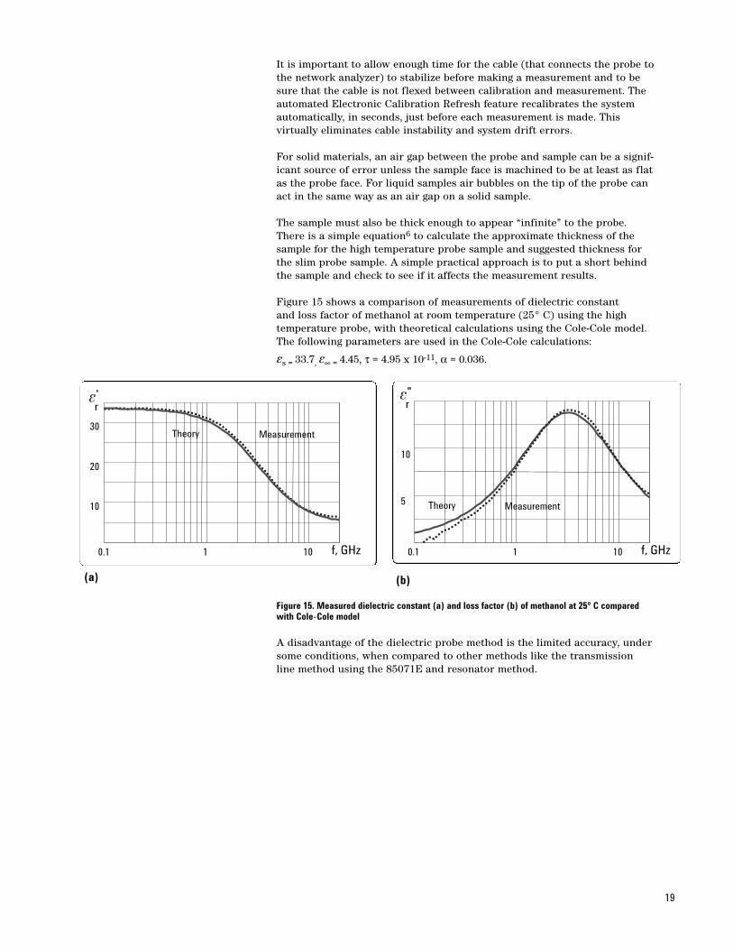
Figure 15 shows a comparison of measurements of dielectric constant and loss factor of methanol at room temperature (25° C) using the high temperature probe, with theoretical calculations using the Cole-Cole model.The following parameters are used in the Cole-Cole calculations:
es = 33.7, e∞ = 4.45, τ = 4.95 x 10⁻¹¹, α = 0.036.
Figure 15. Measured dielectric constant (a) and loss factor (b) of methanol at 25º C comparedwith Cole-Cole model
A disadvantage of the dielectric probe method is the limited accuracy, undersome conditions, when compared to other methods like the transmissionline method using the 85071E and resonator method.
19
0.1 1 10
10
20
30Theory Measurement
f, GHz
'r
e
0.1 1 10
5
10
Theory Measurement
f, GHz
"r
e
(a) (b)
20
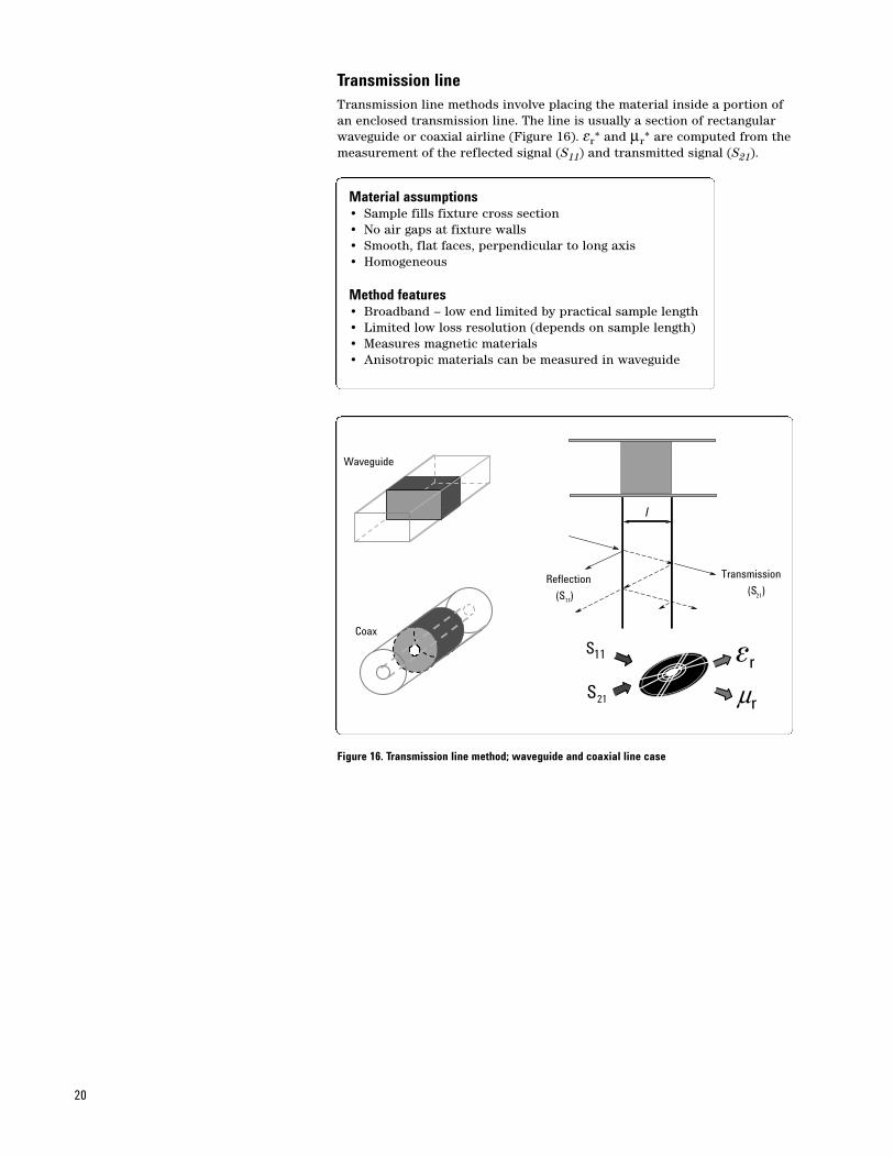
Transmission lineTransmission line methods involve placing the material inside a portion ofan enclosed transmission line. The line is usually a section of rectangularwaveguide or coaxial airline (Figure 16). er* and µr* are computed from themeasurement of the reflected signal (S11) and transmitted signal (S21).
Material assumptions• Sample fills fixture cross section• No air gaps at fixture walls• Smooth, flat faces, perpendicular to long axis• Homogeneous
Method features• Broadband – low end limited by practical sample length• Limited low loss resolution (depends on sample length)• Measures magnetic materials• Anisotropic materials can be measured in waveguide
Figure 16. Transmission line method; waveguide and coaxial line case
l
Reflection
(S )11
Transmission
(S )21
r
rµ
11S
21S
e
Waveguide
Coax
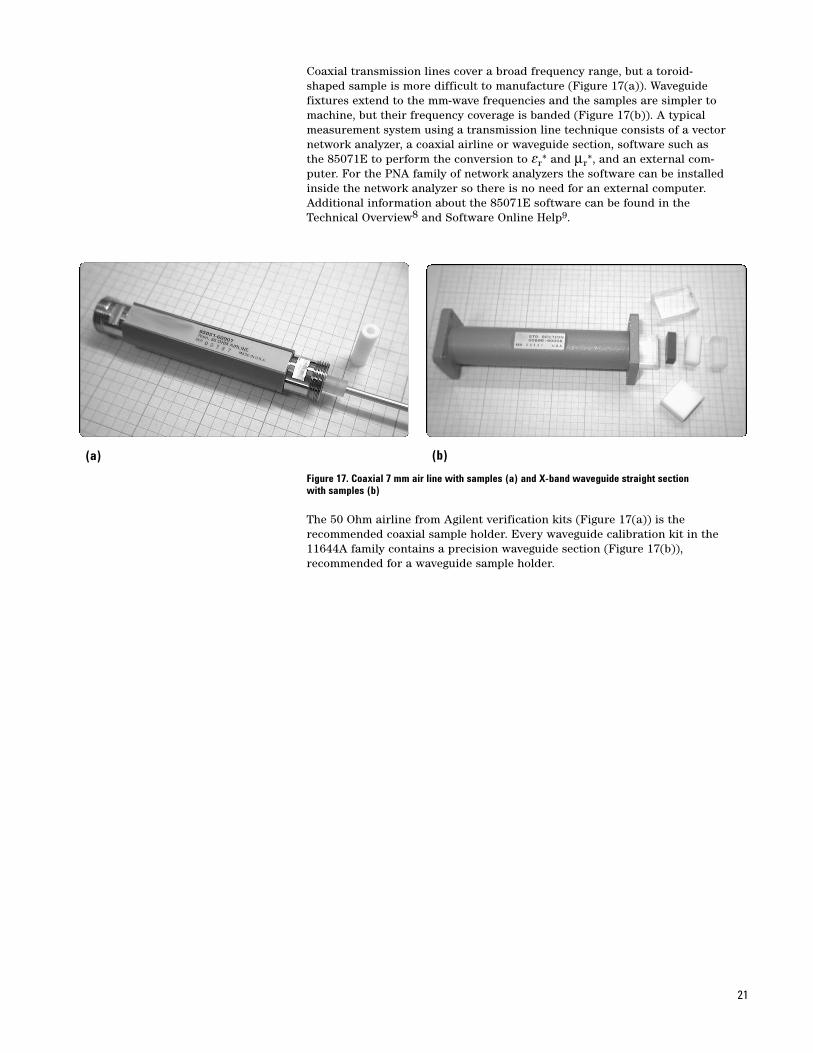
Coaxial transmission lines cover a broad frequency range, but a toroid-shaped sample is more difficult to manufacture (Figure 17(a)). Waveguidefixtures extend to the mm-wave frequencies and the samples are simpler tomachine, but their frequency coverage is banded (Figure 17(b)). A typicalmeasurement system using a transmission line technique consists of a vectornetwork analyzer, a coaxial airline or waveguide section, software such asthe 85071E to perform the conversion to er* and µr*, and an external com-puter. For the PNA family of network analyzers the software can be installedinside the network analyzer so there is no need for an external computer.Additional information about the 85071E software can be found in theTechnical Overview8 and Software Online Help9.
Figure 17. Coaxial 7 mm air line with samples (a) and X-band waveguide straight section with samples (b)
The 50 Ohm airline from Agilent verification kits (Figure 17(a)) is the recommended coaxial sample holder. Every waveguide calibration kit in the11644A family contains a precision waveguide section (Figure 17(b)), recommended for a waveguide sample holder.
21
(a) (b)

Figure 18 shows measurement results of permittivity (a) and loss tangent (b)of two Plexiglas samples with lengths of 25 mm and 31 mm respectively, inan X-band waveguide. The sample holder is the precise waveguide section of140 mm length that is provided with the X11644A calibration kit (Figure 17(b)).The network analyzer is a PNA, the calibration type is TRL and the precisionNIST algorithm9 is used for calculation. In both graphs below there are twopairs of traces for two different measurements of the same samples. The top two measurements of each graph are performed for the case when thesample holder is not calibrated out.
Figure 18. Measurement of two Plexiglas samples, 25 mm and 31 mm long in a X-band waveguide
In this case based on the sample length and sample holder length, the 85071Esoftware will rotate the calibration plane correctly to the sample face, butwill not compensate for the losses of the waveguide. The bottom two measurements of the same samples are performed for the case when thesample holder is part of the calibration and the waveguide losses and electrical length are calibrated out. As expected, the loss tangent curves (b)show lower values when the sample holder is calibrated out and they aremore constant with respect to frequency. This is due to the fact that thewaveguide losses are no longer added to the sample’s losses. With the PNAnetwork analyzer, besides calibrating out the sample holder, it is possible toperform fixture de-embedding, which will lead to the same results. Thisapproach requires measuring the empty sample holder after the calibration.
22
25 mm
25 mm
31 mm
31 mm calibrated out sample holder
9 10 11 122.54
2.56
2.58
f, GHz
'r
e
9 10 11 120.003
0.004
0.005
25 mm
25 mm
31 mm
31 mm
f, GHz
calibrated out sample holder
tan d
(a) (b)
Free space
Material assumptions• Large, flat, parallel-faced samples• Homogeneous
Method features• Non-contacting, non-destructive• High frequency – low end limited by practical sample size• Useful for high temperature• Antenna polarization may be varied for anisotropic materials• Measures magnetic materials
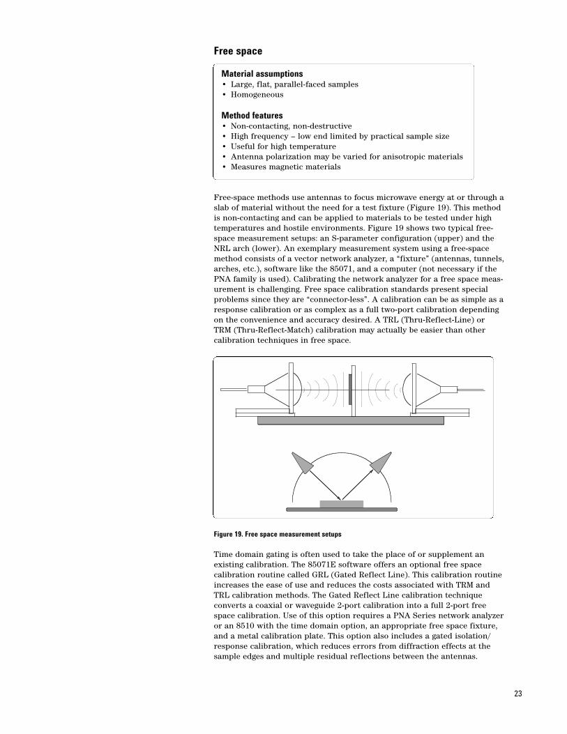
Free-space methods use antennas to focus microwave energy at or through aslab of material without the need for a test fixture (Figure 19). This methodis non-contacting and can be applied to materials to be tested under hightemperatures and hostile environments. Figure 19 shows two typical free-space measurement setups: an S-parameter configuration (upper) and theNRL arch (lower). An exemplary measurement system using a free-spacemethod consists of a vector network analyzer, a “fixture” (antennas, tunnels,arches, etc.), software like the 85071, and a computer (not necessary if thePNA family is used). Calibrating the network analyzer for a free space meas-urement is challenging. Free space calibration standards present special problems since they are “connector-less”. A calibration can be as simple as aresponse calibration or as complex as a full two-port calibration dependingon the convenience and accuracy desired. A TRL (Thru-Reflect-Line) or TRM (Thru-Reflect-Match) calibration may actually be easier than other calibration techniques in free space.
Figure 19. Free space measurement setups
Time domain gating is often used to take the place of or supplement anexisting calibration. The 85071E software offers an optional free space calibration routine called GRL (Gated Reflect Line). This calibration routineincreases the ease of use and reduces the costs associated with TRM andTRL calibration methods. The Gated Reflect Line calibration technique converts a coaxial or waveguide 2-port calibration into a full 2-port freespace calibration. Use of this option requires a PNA Series network analyzeror an 8510 with the time domain option, an appropriate free space fixture,and a metal calibration plate. This option also includes a gated isolation/response calibration, which reduces errors from diffraction effects at thesample edges and multiple residual reflections between the antennas.
23

Accurate free space measurements are now possible without expensive spotfocusing antennas, micro positioning fixtures, or direct receiver access. The85070E software automatically sets up all the free space calibration definitions and network analyzer parameters, saving engineering time. Withthe PNA, additional ease and time savings is provided with ECal, electroniccalibration. A guided calibration wizard steps the user through the easy calibration process. Figure 20 depicts the result of a GRL calibration meas-uring Rexolite material in U-band (40-60 GHz) with a PNA network analyzerand 85071E software. The fixture is made from a readily available, domesticuse, shelving unit to demonstrate that when doing a GRL calibration, evenwith the simplest set up, it is still possible to perform precise measurements.
Figure 20. Measurement of Rexolite sample in a U-band (40 – 60 GHz)
High temperature measurements are easy to perform in free space since thesample is never touched or contacted (Figure 21). The sample can be heatedby placing it within a furnace that has “windows” of insulation material thatare transparent to microwaves. Agilent Technologies does not provide thefurnace needed for such a type of measurement. Figure 21 illustrates thebasic set up.
Figure 21. High temperature measurement in free space
24
45 50 552.4
2.5
2.6
f, GHz
'r
e
Heating panels
Sample
Thermalinsulation
Thermocouple
Furnace
Resonant cavityResonant versus broadband techniques
Resonant techniques• High impedance environment• Reasonable measurements possible with small samples• Measurements at only one or a few frequencies• Well suited for low loss materials
Broadband techniques• Low impedance environment• Requires larger samples to obtain reasonable measurements• Measurement at “any” frequency
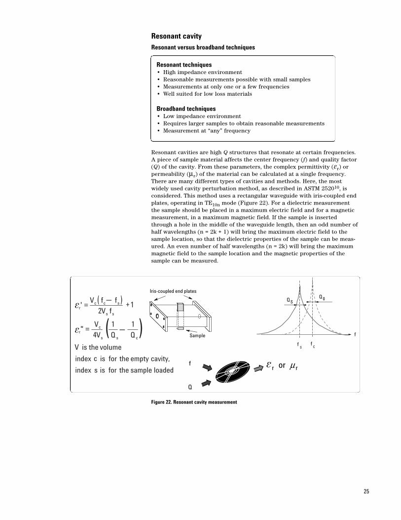
Resonant cavities are high Q structures that resonate at certain frequencies.A piece of sample material affects the center frequency (f) and quality factor(Q) of the cavity. From these parameters, the complex permittivity (er) orpermeability (µr) of the material can be calculated at a single frequency.There are many different types of cavities and methods. Here, the mostwidely used cavity perturbation method, as described in ASTM 252010, isconsidered. This method uses a rectangular waveguide with iris-coupled endplates, operating in TE10n mode (Figure 22). For a dielectric measurementthe sample should be placed in a maximum electric field and for a magneticmeasurement, in a maximum magnetic field. If the sample is insertedthrough a hole in the middle of the waveguide length, then an odd number ofhalf wavelengths (n = 2k + 1) will bring the maximum electric field to thesample location, so that the dielectric properties of the sample can be meas-ured. An even number of half wavelengths (n = 2k) will bring the maximummagnetic field to the sample location and the magnetic properties of thesample can be measured.
Figure 22. Resonant cavity measurement
25
Q 0
fC
f
Q S
fS
f
Q
rr or µ
Sample
Iris-coupled end plates
e
( )
loadedsampletheforissindex
cavityemptytheforiscindex
volumetheisV
QQV
V
fV
ffV
css
cr
ss
sccr
,
11
4"
2'
=
=e
e
–
–( )+1
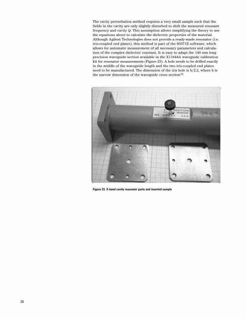
The cavity perturbation method requires a very small sample such that thefields in the cavity are only slightly disturbed to shift the measured resonantfrequency and cavity Q. This assumption allows simplifying the theory to usethe equations above to calculate the dielectric properties of the material.Although Agilent Technologies does not provide a ready-made resonator (i.e. iris-coupled end plates), this method is part of the 85071E software, whichallows for automatic measurement of all necessary parameters and calcula-tion of the complex dielectric constant. It is easy to adapt the 140 mm longprecision waveguide section available in the X11644A waveguide calibrationkit for resonator measurements (Figure 23). A hole needs to be drilled exactlyin the middle of the waveguide length and the two iris-coupled end platesneed to be manufactured. The dimension of the iris hole is b/2.2, where b isthe narrow dimension of the waveguide cross section10.
Figure 23. X-band cavity resonator parts and inserted sample
26
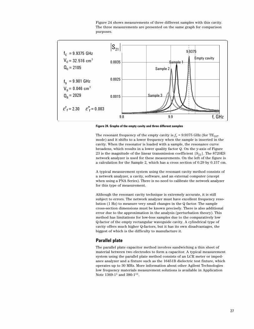
Figure 24 shows measurements of three different samples with this cavity.The three measurements are presented on the same graph for comparisonpurposes.
Figure 24. Graphs of the empty cavity and three different samples
The resonant frequency of the empty cavity is fc = 9.9375 GHz (for TE107mode) and it shifts to a lower frequency when the sample is inserted in thecavity. When the resonator is loaded with a sample, the resonance curvebroadens, which results in a lower quality factor Q. On the y-axis of Figure23 is the magnitude of the linear transmission coefficient |S21|. The 8720ESnetwork analyzer is used for these measurements. On the left of the figure isa calculation for the Sample 2, which has a cross section of 0.29 by 0.157 cm.
A typical measurement system using the resonant cavity method consists ofa network analyzer, a cavity, software, and an external computer (exceptwhen using a PNA Series). There is no need to calibrate the network analyzerfor this type of measurement.
Although the resonant cavity technique is extremely accurate, it is still subject to errors. The network analyzer must have excellent frequency reso-lution (1 Hz) to measure very small changes in the Q factor. The samplecross-section dimensions must be known precisely. There is also additionalerror due to the approximation in the analysis (perturbation theory). Thismethod has limitations for low-loss samples due to the comparatively low Q-factor of the empty rectangular waveguide cavity. A cylindrical type ofcavity offers much higher Q-factors, but it has its own disadvantages, thebiggest of which is the difficulty to manufacture it.
Parallel plateThe parallel plate capacitor method involves sandwiching a thin sheet ofmaterial between two electrodes to form a capacitor. A typical measurementsystem using the parallel plate method consists of an LCR meter or imped-ance analyzer and a fixture such as the 16451B dielectric test fixture, whichoperates up to 30 MHz. More information about other Agilent Technologieslow frequency materials measurement solutions is available in ApplicationNote 1369-11 and 380-111.
27
9.8 9.9
0.0015
0.0025
0.0035
9.9375
Empty cavitySample 1
Sample 2
Sample 3
f, GHz
21S
003.02.30
2029
cm046.0
GHz901.9
2105
cm516.32
GHz9375.9
3
3
==
=
=
=
=
=
=fcVc
Qc
fsVs
Qs
're "re
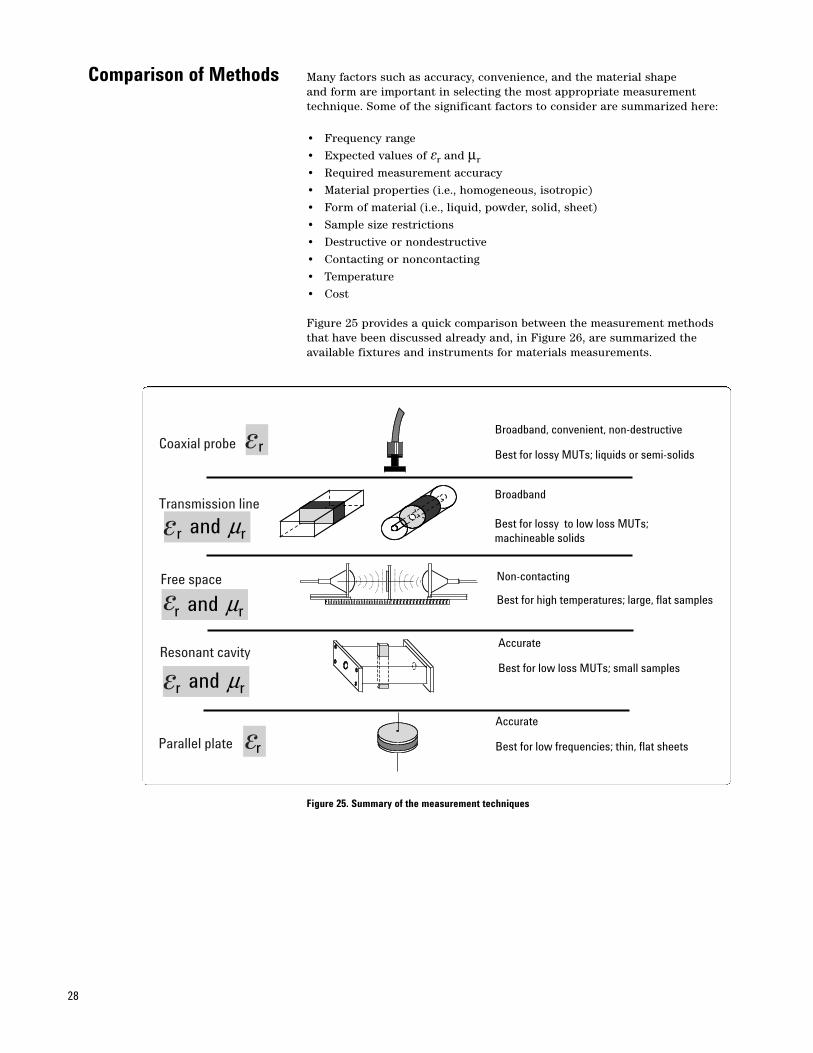
Comparison of Methods Many factors such as accuracy, convenience, and the material shape and form are important in selecting the most appropriate measurementtechnique. Some of the significant factors to consider are summarized here:
• Frequency range
• Expected values of er and µr
• Required measurement accuracy
• Material properties (i.e., homogeneous, isotropic)
• Form of material (i.e., liquid, powder, solid, sheet)
• Sample size restrictions
• Destructive or nondestructive
• Contacting or noncontacting
• Temperature
• Cost
Figure 25 provides a quick comparison between the measurement methodsthat have been discussed already and, in Figure 26, are summarized theavailable fixtures and instruments for materials measurements.
Figure 25. Summary of the measurement techniques
28
Coaxial probe
Transmission line
Best for lossy MUTs; liquids or semi-solids
Broadband, convenient, non-destructive
Best for lossy to low loss MUTs; machineable solids
Broadband
rr and µ
r
Resonant cavityBest for low loss MUTs; small samples
Accurate
rr and µ
Free spaceBest for high temperatures; large, flat samples
Non-contacting
rr and µ
Parallel plate Best for low frequencies; thin, flat sheets
Accurate
r
e
e
e
e
e
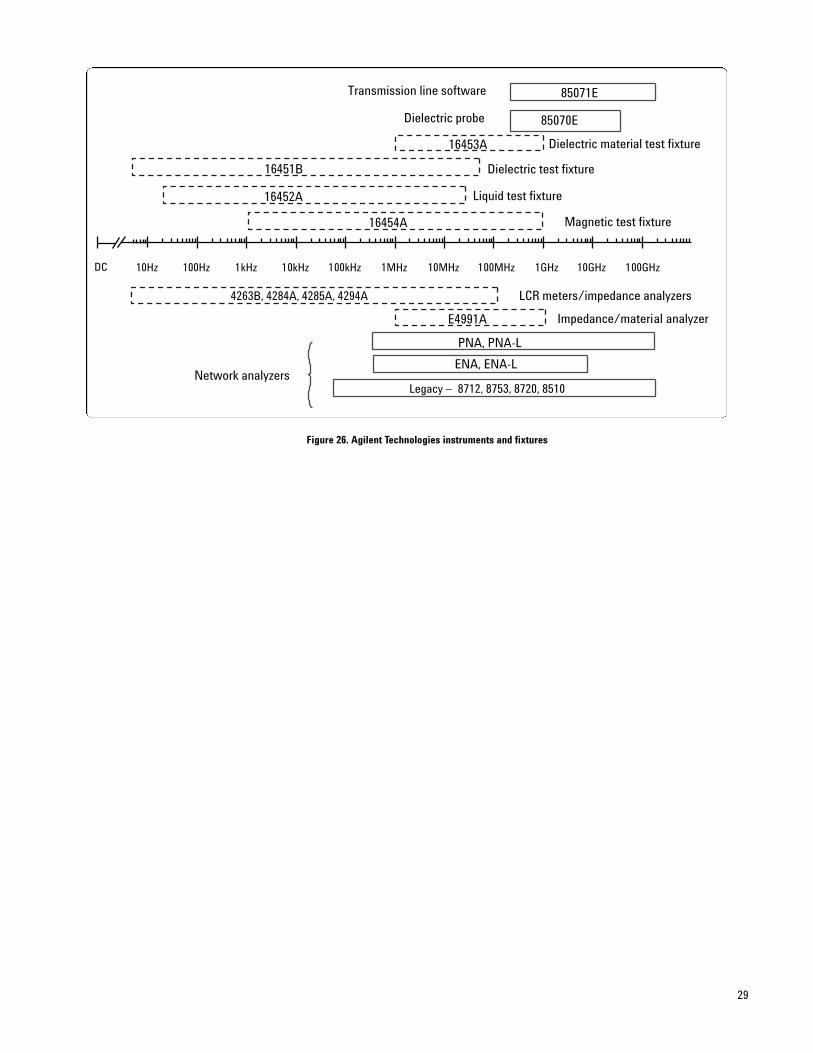
Figure 26. Agilent Technologies instruments and fixtures
29
10Hz 100Hz 1kHz 10kHz 100kHz 1MHz 10MHz 100MHz 1GHz 10GHz 100GHz
Legacy – 8712, 8753, 8720, 8510
ENA, ENA-L
85070E
85071E
4263B, 4284A, 4285A, 4294A
16451B Dielectric test fixture
Dielectric probe
Transmission line software
LCR meters/impedance analyzers
Network analyzers
DC
16452A Liquid test fixture
E4991A Impedance/material analyzer
16453A Dielectric material test fixture
PNA, PNA-L
16454A Magnetic test fixture

References 1. Application Note 1369-1, Solutions for Measuring Permittivity and Permeability with LCR Meters and Impedance Analyzers, Agilent Literature Number 5980-2862EN, May 6, 2003
2. Application note 1287-1, Understanding the Fundamental Principles of Vector Network Analysis, Agilent literature number 5965-7707E, 2000
3. Application note 1287-2, Exploring the Architectures of Network Analyzers, Agilent literature number 5965-7708E, December 6, August 2000
4. Application note 1287-3, Applying Error Correction to Network Analyzer Measurements, Agilent literature number 5965-7709E, March 27, 2002
5. D. V. Blackham, R. D. Pollard, An Improved Technique for Permittivity Measurements Using a Coaxial Probe, IEEE Trans. on Instr. Meas., vol. 46, No 5, Oct. 1997, pp. 1093- 1099
6. Technical Overview, Agilent 85071E Materials Measurement Software,Agilent literature number 5989-0222EN, November 6, 2003
7. Online Help for 85070 software
8. Technical Overview, Agilent 85070E Dielectric Probe Kit 200 MHz to 50 GHz, Agilent literature number 5988-9472EN, May 9, 2003
9. Online Help for 85071 software
10. ASTM Test methods for complex permittivity (Dielectric Constant) of solid electrical insulating materials at microwave frequencies and temperatures to 1650°, ASTM Standard D2520, American Society for Testing and Materials
11. Application Note 380-1, Dielectric constant measurement of solid materials using the 16451B dielectric test fixture, Agilent literature number 5950-2390, September 1998
30
Additional References • Altschuler H.M., Dielectric Constant, Chapter IX of Handbook of Microwave Measurements, M. Sucher and J. Fox ed., Wiley 1963
• Arthur von Hippel (ed), Dielectric Materials and Applications,Cambridge, Massachusetts: MIT Press, 3rd printing, January 1961
• J. Baker-Jarvis, M. D. Janezic, J. S. Grosvenor, R. G. Geyer, Transmission/ Reflection and Short-Circuit Methods for Measuring Permitivity and Permeability, NIST Technical Note 1355-R, December 1993
• H. E. Bussey, Measurement of RF properties of materials-A survey, Proc. IEEE, vol. 55, No. 6, pp. 1046-1053, June 1967.
• A. C. Lynch, Precise measurements on dielectric and magnetic materials,IEEE Trans. on Instrum. Meas., vol. IM-23, No. 4, Dec. 1974, pp. 425-43
• M. Afsar, J.B. Birch, R.N. Clarke, Ed. G.W. Chantry; Measurement of the Properties of Materials, Proc. IEEE, vol. 74, No 1, pp. 183-199. Jan 1986
• A. M. Nicolson, G. F. Ross, Measurement of the intrinsic properties of materials by time-domain techniques, IEEE Trans. on Instrum. Meas., vol. IM-19, Nov 1970, pp. 377-82
• W. B. Weir, Automatic measurement of complex dielectric constant and permeability at microwave frequencies, Proc. IEEE, vol. 62, no. 1, pp. 33-36, Jan. 1974.
31

Web Resources
Visit our web sites for additional product information and literature.
Materials Test Equipment:www.agilent.com/find/materials
Network Analyzers:www.agilent.com/find/na
Electronic Calibration (ECal) modules:www.agilent.com/find/ecal
www.agilent.comAgilent Technologies’ Test and Measurement Support,Services, and AssistanceAgilent Technologies aims to maximize the value youreceive, while minimizing your risk and problems. We strive to ensure that you get the test and measurementcapabilities you paid for and obtain the support you need.Our extensive support resources and services can help you choose the right Agilent products for your applicationsand apply them successfully. Every instrument and systemwe sell has a global warranty. Two concepts underlieAgilent’s overall support policy: “Our Promise” and “YourAdvantage.”
Our PromiseOur Promise means your Agilent test and measurementequipment will meet its advertised performance and functionality. When you are choosing new equipment, wewill help you with product information, including realisticperformance specifications and practical recommendationsfrom experienced test engineers. When you receive yournew Agilent equipment, we can help verify that it worksproperly and help with initial product operation.
Your AdvantageYour Advantage means that Agilent offers a wide range ofadditional expert test and measurement services, whichyou can purchase according to your unique technical andbusiness needs. Solve problems efficiently and gain a competitive edge by contracting with us for calibration,extra-cost upgrades, out-of-warranty repairs, and onsiteeducation and training, as well as design, system integra-tion, project management, and other professional engineer-ing services. Experienced Agilent engineers and techniciansworldwide can help you maximize your productivity, opti-mize the return on investment of your Agilent instrumentsand systems, and obtain dependable measurement accura-cy for the life of those products.
For more information on Agilent Technologies’ products,applications or services, please contact your localAgilent office.
Phone or Fax
United States: Korea:(tel) 800 829 4444 (tel) (080) 769 0800(fax) 800 829 4433 (fax) (080)769 0900Canada: Latin America:(tel) 877 894 4414 (tel) (305) 269 7500(fax) 800 746 4866 Taiwan:China: (tel) 0800 047 866(tel) 800 810 0189 (fax) 0800 286 331(fax) 800 820 2816 Other Asia PacificEurope: Countries:(tel) 31 20 547 2111 (tel) (65) 6375 8100Japan: (fax) (65) 6755 0042(tel) (81) 426 56 7832 Email: [email protected](fax) (81) 426 56 7840 Contacts revised: 05/27/05
The complete list is available at:www.agilent.com/find/contactus
Product specifications and descriptions in this document subject to change without notice.
© Agilent Technologies, Inc. 2005, 2006Printed in USA, June 26, 20065989-2589EN
www.agilent.com/find/emailupdatesGet the latest information on the products andapplications you select.
Agilent Email Updates
www.agilent.com/find/agilentdirectQuickly choose and use your test equipment solutions with confidence.
Agilent Direct
Agilent Open
www.agilent.com/find/openAgilent Open simplifies the process of connectingand programming test systems to help engineersdesign, validate and manufacture electronic products.Agilent offers open connectivity for a broad range ofsystem-ready instruments, open industry software,PC-standard I/O and global support, which are com-bined to more easily integrate test system develop-ment.


![Dielectric Properties of Biological Tissue: A Review on ...cost-emf-med.eu/wp-content/uploads/2016/04/Dielectric-Properties... · Thank you! References: [1] Note, Application. "Basics](https://static.fdocuments.net/doc/165x107/5b156d127f8b9ac7128c68d0/dielectric-properties-of-biological-tissue-a-review-on-cost-emf-medeuwp-contentuploads201604dielectric-properties.jpg)