


Languages
Pages
Legal

VLSI DesignLecture 2: Basic Fabrication Steps and
Layout
Mohammad Arjomand
CE Department
Sharif Univ. of Tech.
Adapted with modifications from Harris’s lecture notes
Modern VLSI Design 4e: Chapter 2 Sharif University of Technology Slide 2 of 50
Outline
How to make a transistor or a gateCross-sectionTop view (masks)Fabrication process
Layout Design rules Standard cell layouts Stick Diagrams

Modern VLSI Design 4e: Chapter 2 Sharif University of Technology Slide 3 of 50
Our technology
We will study a generic 180 nm technology (SCMOS rules).Assume 1.2V supply voltage.
Parameters are typical values. Parameter sets/Spice models are often available for 180
nm, harder to find for 90 nm.

Modern VLSI Design 4e: Chapter 2 Sharif University of Technology Slide 4 of 50
Fabrication services
Educational services:U.S.: MOSIS (has defined SCMOS rules)EC: EuroPracticeTaiwan: CICJapan: VDEC
Foundry = fabrication line for hire.Foundries are major source of fab capacity today.

Modern VLSI Design 4e: Chapter 2 Sharif University of Technology Slide 5 of 50
Silicon Lattice
Transistors are built on a silicon substrate Silicon is a Group IV material Forms crystal lattice with bonds to four neighbors
Si SiSi
Si SiSi
Si SiSi

Modern VLSI Design 4e: Chapter 2 Sharif University of Technology Slide 6 of 50
Dopants
Silicon is a semiconductor Pure silicon has no free carriers and conducts poorly Adding dopants increases the conductivity Group V (Arsenic, Phosphorus): extra electron (n-type) Group III (Boron): missing electron, called hole (p-type)
As SiSi
Si SiSi
Si SiSi
B SiSi
Si SiSi
Si SiSi
-
+
+
-

Modern VLSI Design 4e: Chapter 2 Sharif University of Technology Slide 7 of 50
p-n Junctions
A junction between p-type and n-type semiconductor forms a diode.
Current flows only in one direction
N-Diff P-Diff
anodecathode
Modern VLSI Design 4e: Chapter 2 Sharif University of Technology Slide 8 of 50
Fabrication processes
IC built on silicon substrate:some structures diffused into substrate;other structures built on top of substrate.
Substrate regions are doped with n-type and p-type impurities. (n+ = heavily doped)
Wires made of polycrystalline silicon (poly), multiple layers of aluminum (metal).
Silicon dioxide (SiO2) is insulator.
Modern VLSI Design 4e: Chapter 2 Sharif University of Technology Slide 9 of 50
CMOS Fabrication
CMOS transistors are fabricated on silicon wafer Lithography process similar to printing press On each step, different materials are deposited or
etched Easiest to understand by viewing both top and cross-
section of wafer in a simplified manufacturing process
Modern VLSI Design 4e: Chapter 2 Sharif University of Technology Slide 10 of 50
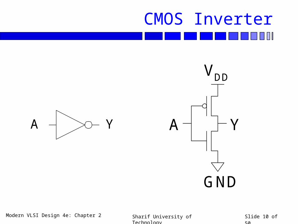
CMOS Inverter
VDD
A Y
GND
A Y
Modern VLSI Design 4e: Chapter 2 Sharif University of Technology Slide 11 of 50
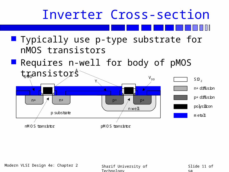
Inverter Cross-section
Typically use p-type substrate for nMOS transistors Requires n-well for body of pMOS transistors
n+
p substrate
p+
n well
A
YGND VDD
n+ p+
SiO2
n+ diffusion
p+ diffusion
polysilicon
metal1
nMOS transistor pMOS transistor
Modern VLSI Design 4e: Chapter 2 Sharif University of Technology Slide 12 of 50
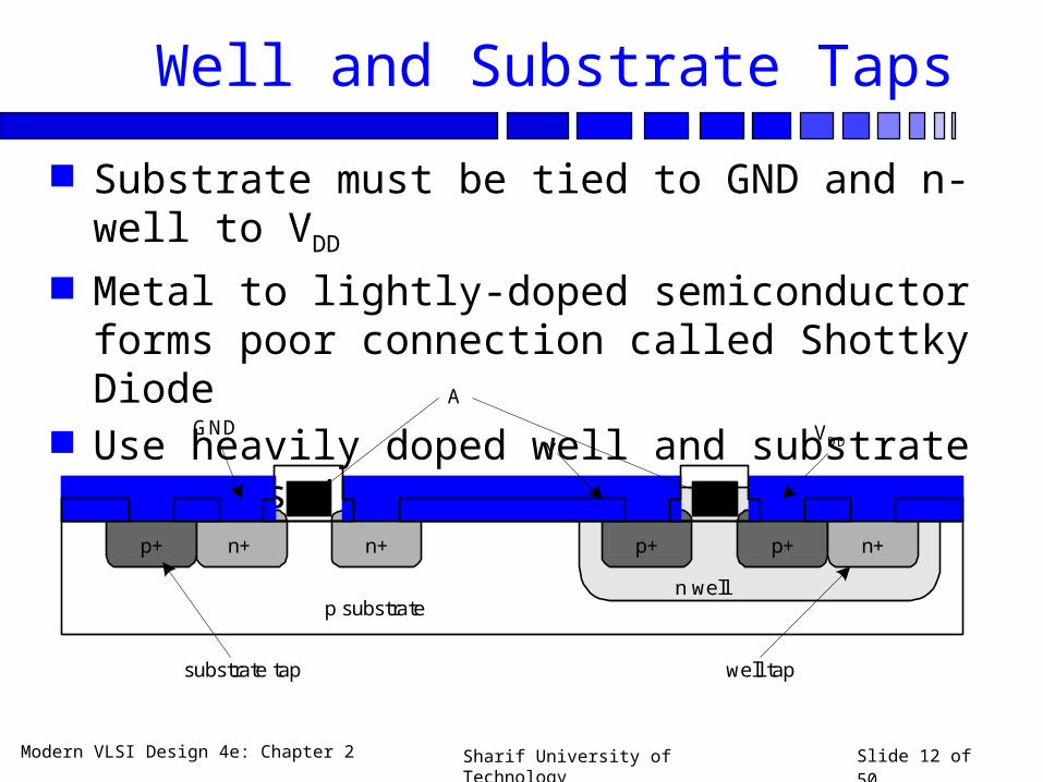
Well and Substrate Taps
Substrate must be tied to GND and n-well to VDD
Metal to lightly-doped semiconductor forms poor connection called Shottky Diode
Use heavily doped well and substrate contacts / taps
n+
p substrate
p+
n well
A
YGND VDD
n+p+
substrate tap well tap
n+ p+
Modern VLSI Design 4e: Chapter 2 Sharif University of Technology Slide 13 of 50
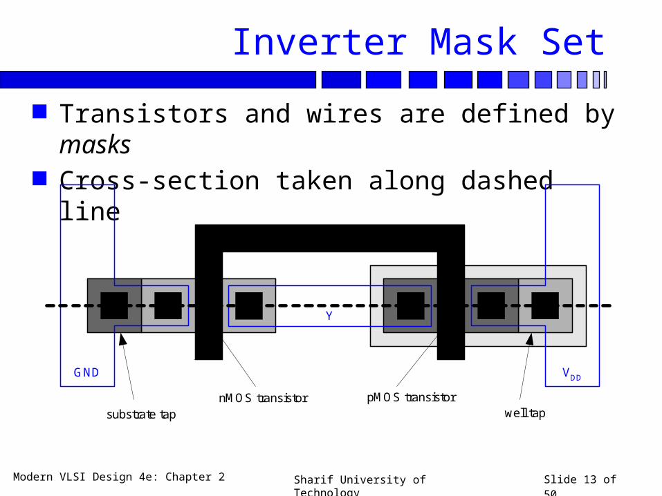
Inverter Mask Set
Transistors and wires are defined by masks Cross-section taken along dashed line
GND VDD
Y
A
substrate tap well tapnMOS transistor pMOS transistor
Modern VLSI Design 4e: Chapter 2 Sharif University of Technology Slide 14 of 50
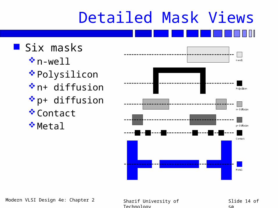
Detailed Mask Views
Six masksn-wellPolysiliconn+ diffusionp+ diffusionContactMetal
Metal
Polysilicon
Contact
n+ Diffusion
p+ Diffusion
n well
Modern VLSI Design 4e: Chapter 2 Sharif University of Technology Slide 15 of 50
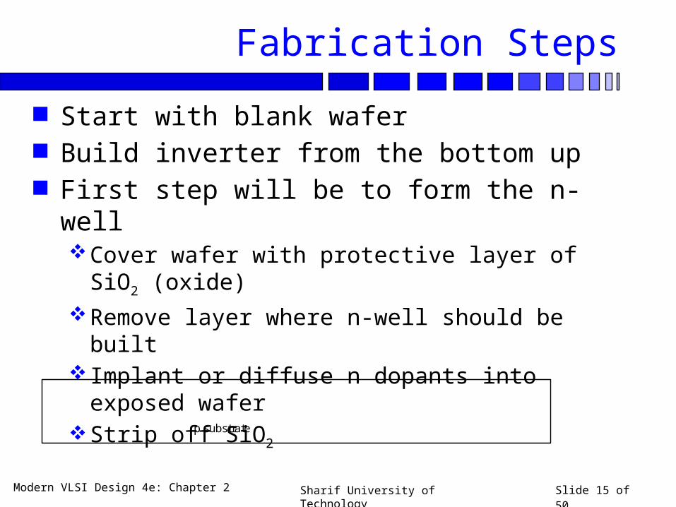
Fabrication Steps
Start with blank wafer Build inverter from the bottom up First step will be to form the n-well
Cover wafer with protective layer of SiO2 (oxide)Remove layer where n-well should be built Implant or diffuse n dopants into exposed waferStrip off SiO2
p substrate

Modern VLSI Design 4e: Chapter 2 Sharif University of Technology Slide 16 of 50
Oxidation
Grow SiO2 on top of Si wafer900 – 1200 C with H2O or O2 in oxidation furnace
p substrate
SiO2

Modern VLSI Design 4e: Chapter 2 Sharif University of Technology Slide 17 of 50
Photoresist
Spin on photoresistPhotoresist is a light-sensitive organic polymerSoftens where exposed to light
p substrate
SiO2
Photoresist
Modern VLSI Design 4e: Chapter 2 Sharif University of Technology Slide 18 of 50
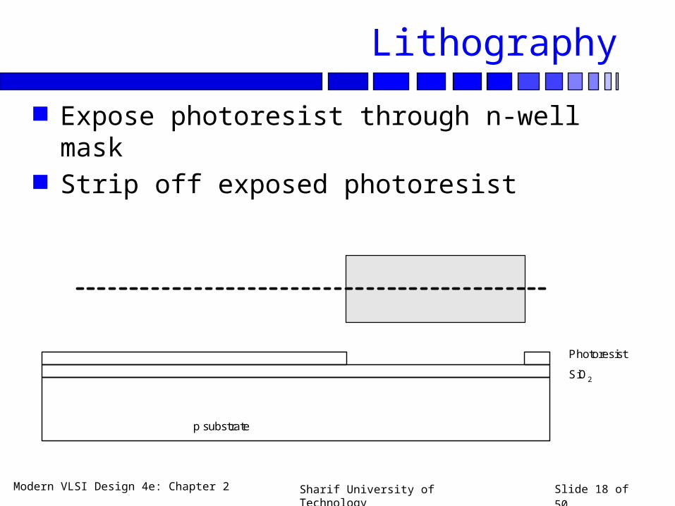
Lithography
Expose photoresist through n-well mask Strip off exposed photoresist
p substrate
SiO2
Photoresist

Modern VLSI Design 4e: Chapter 2 Sharif University of Technology Slide 19 of 50
Etch
Etch oxide with hydrofluoric acid (HF)Seeps through skin and eats bone; nasty stuff!!!
Only attacks oxide where resist has been exposed
p substrate
SiO2
Photoresist
Modern VLSI Design 4e: Chapter 2 Sharif University of Technology Slide 20 of 50
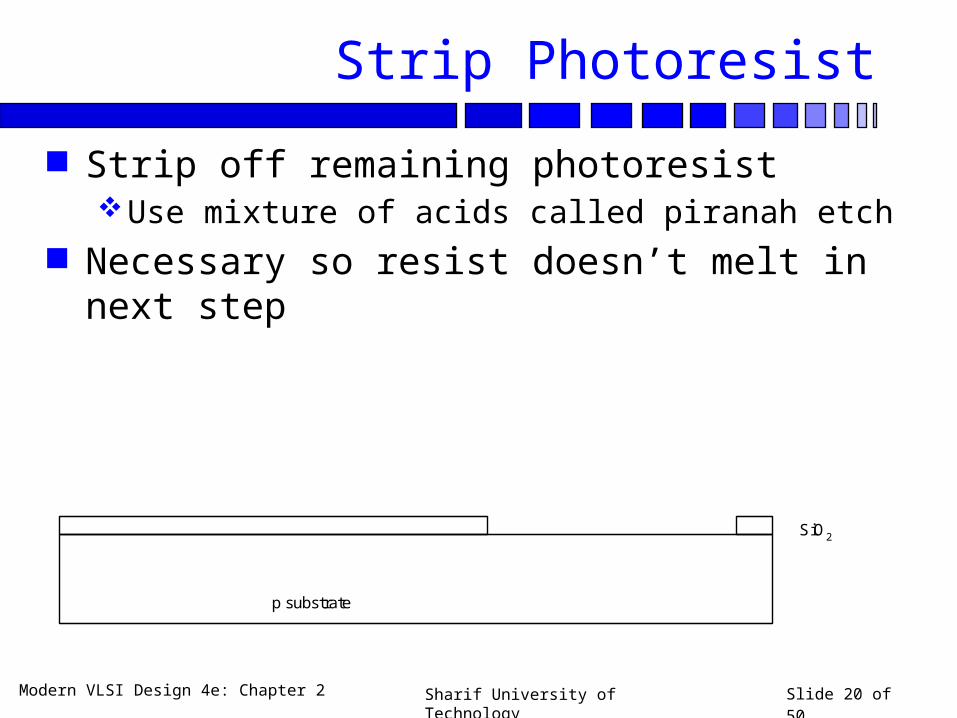
Strip Photoresist
Strip off remaining photoresistUse mixture of acids called piranah etch
Necessary so resist doesn’t melt in next step
p substrate
SiO2
Modern VLSI Design 4e: Chapter 2 Sharif University of Technology Slide 21 of 50
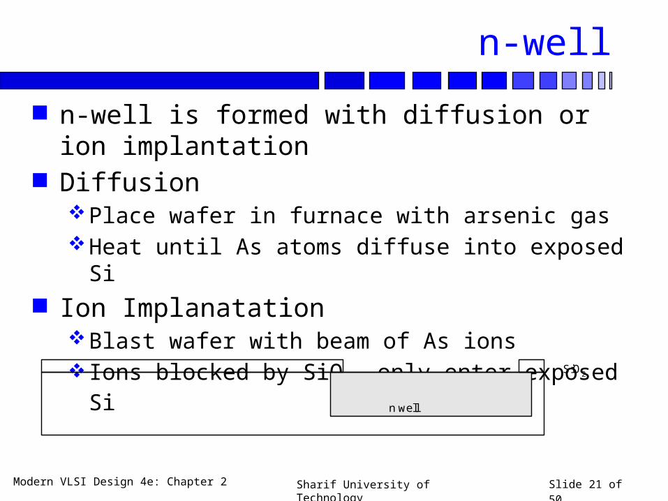
n-well
n-well is formed with diffusion or ion implantation Diffusion
Place wafer in furnace with arsenic gasHeat until As atoms diffuse into exposed Si
Ion ImplanatationBlast wafer with beam of As ions Ions blocked by SiO2, only enter exposed Si
n well
SiO2
Modern VLSI Design 4e: Chapter 2 Sharif University of Technology Slide 22 of 50
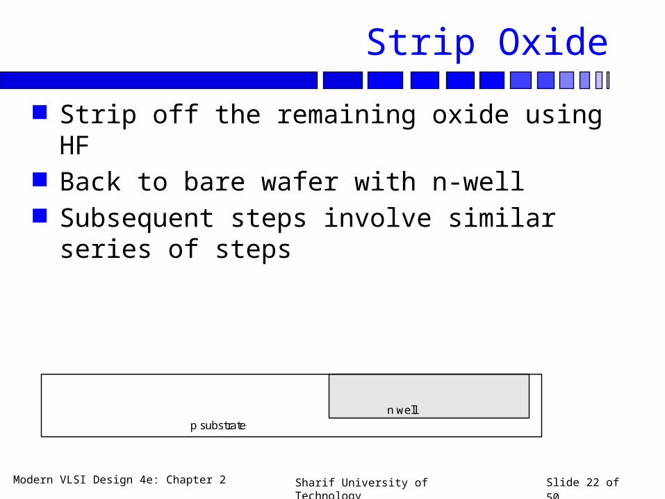
Strip Oxide
Strip off the remaining oxide using HF Back to bare wafer with n-well Subsequent steps involve similar series of steps
p substraten well
Modern VLSI Design 4e: Chapter 2 Sharif University of Technology Slide 23 of 50
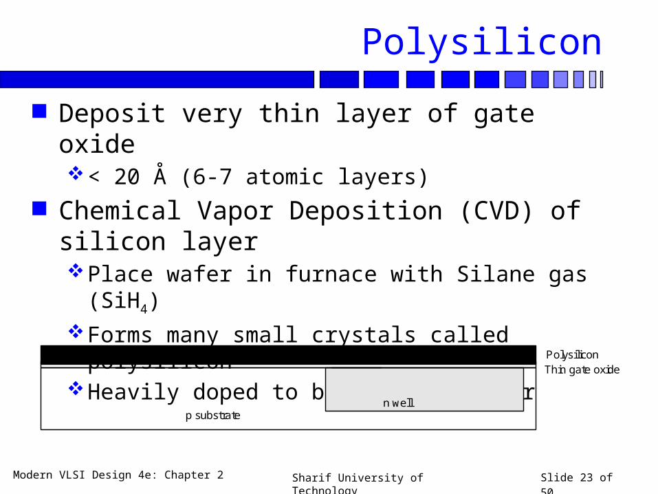
Polysilicon
Deposit very thin layer of gate oxide< 20 Å (6-7 atomic layers)
Chemical Vapor Deposition (CVD) of silicon layerPlace wafer in furnace with Silane gas (SiH4)Forms many small crystals called polysiliconHeavily doped to be good conductor
Thin gate oxidePolysilicon
p substraten well
Modern VLSI Design 4e: Chapter 2 Sharif University of Technology Slide 24 of 50
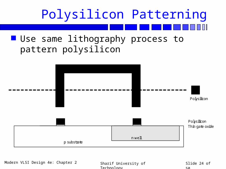
Polysilicon Patterning
Use same lithography process to pattern polysilicon
Polysilicon
p substrate
Thin gate oxidePolysilicon
n well
Modern VLSI Design 4e: Chapter 2 Sharif University of Technology Slide 25 of 50
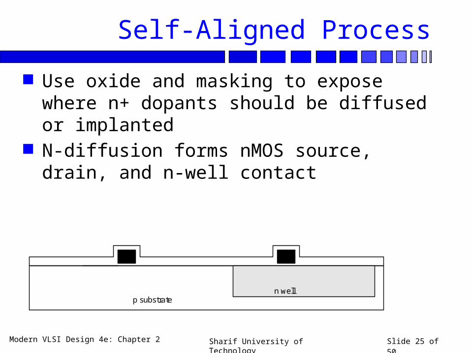
Self-Aligned Process
Use oxide and masking to expose where n+ dopants should be diffused or implanted
N-diffusion forms nMOS source, drain, and n-well contact
p substraten well
Modern VLSI Design 4e: Chapter 2 Sharif University of Technology Slide 26 of 50
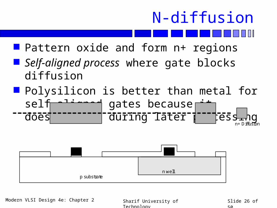
N-diffusion
Pattern oxide and form n+ regions Self-aligned process where gate blocks diffusion Polysilicon is better than metal for self-aligned gates
because it doesn’t melt during later processing
p substraten well
n+ Diffusion
Modern VLSI Design 4e: Chapter 2 Sharif University of Technology Slide 27 of 50
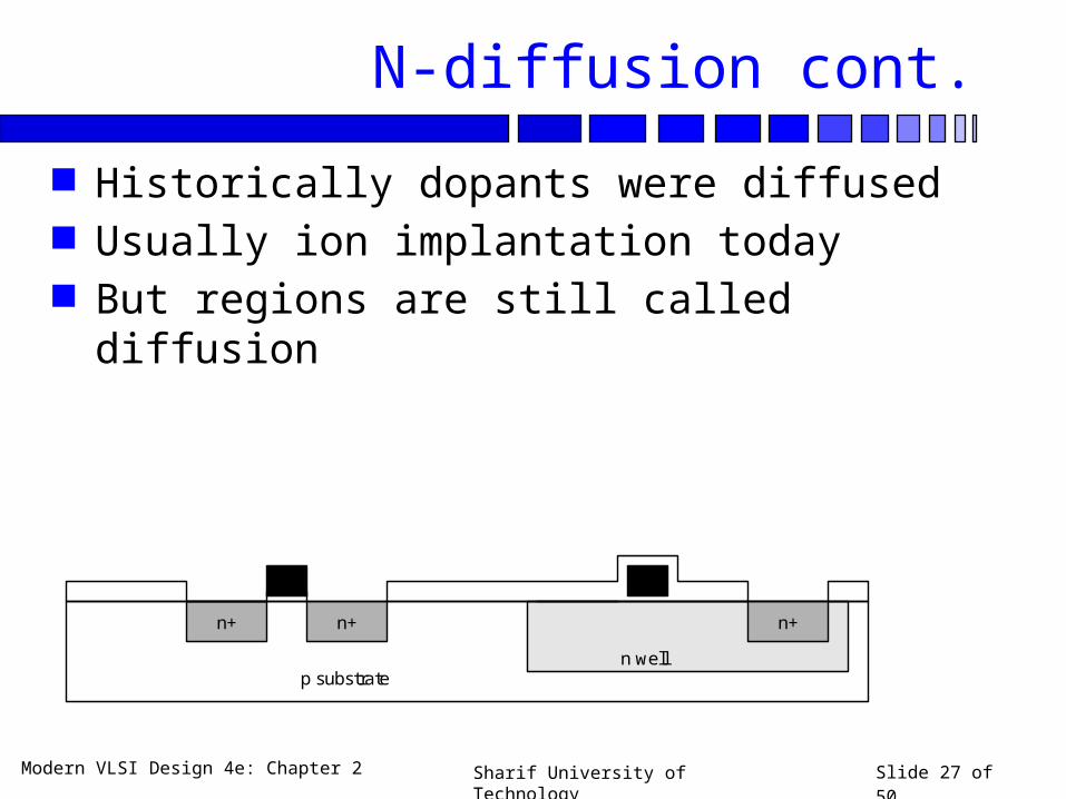
N-diffusion cont.
Historically dopants were diffused Usually ion implantation today But regions are still called diffusion
n wellp substrate
n+n+ n+
Modern VLSI Design 4e: Chapter 2 Sharif University of Technology Slide 28 of 50
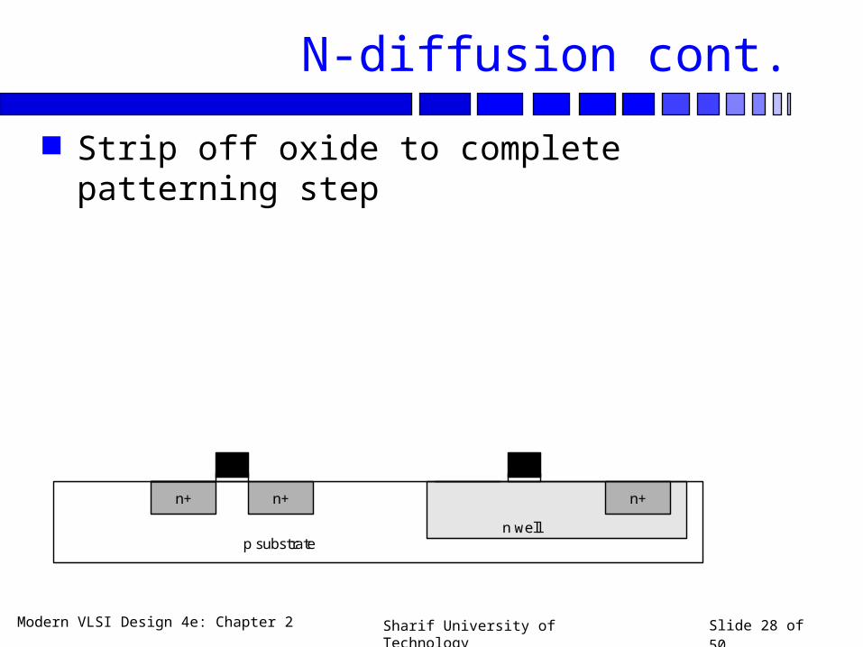
N-diffusion cont.
Strip off oxide to complete patterning step
n wellp substrate
n+n+ n+
Modern VLSI Design 4e: Chapter 2 Sharif University of Technology Slide 29 of 50
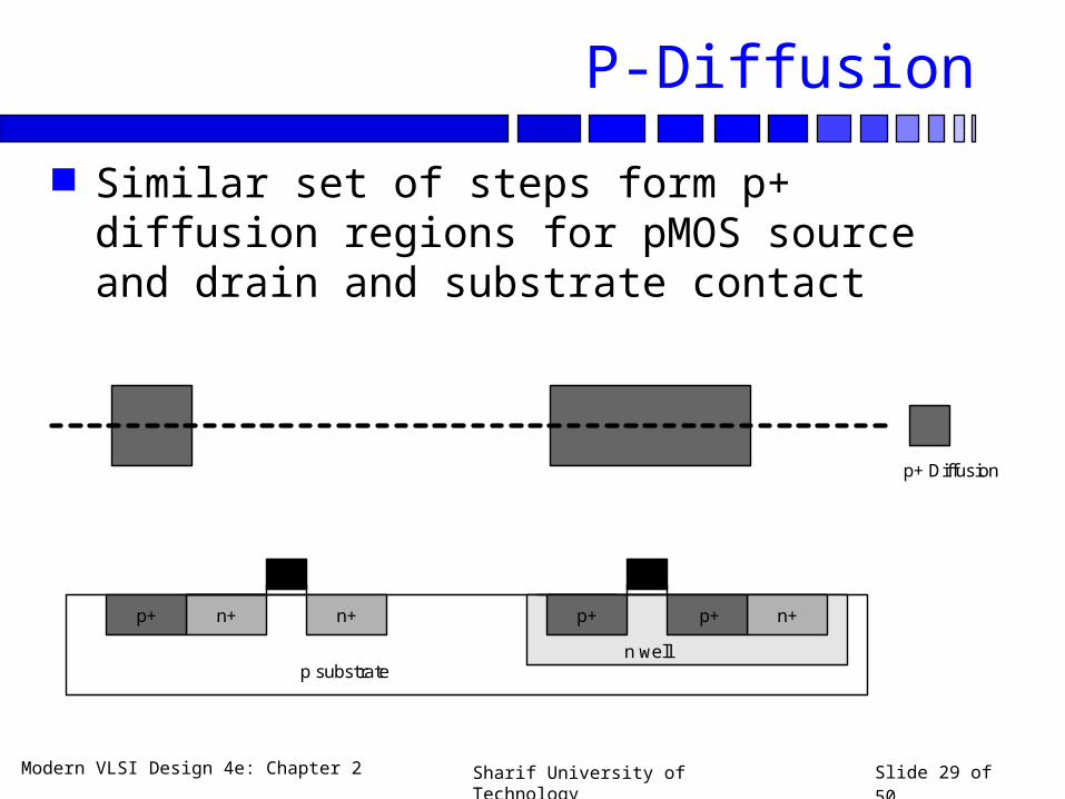
P-Diffusion
Similar set of steps form p+ diffusion regions for pMOS source and drain and substrate contact
p+ Diffusion
p substraten well
n+n+ n+p+p+p+

Modern VLSI Design 4e: Chapter 2 Sharif University of Technology Slide 30 of 50
Contacts
Now we need to wire together the devices Cover chip with thick field oxide Etch oxide where contact cuts are needed
p substrate
Thick field oxide
n well
n+n+ n+p+p+p+
Contact
Modern VLSI Design 4e: Chapter 2 Sharif University of Technology Slide 31 of 50
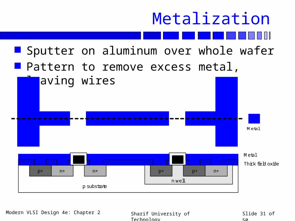
Metalization
Sputter on aluminum over whole wafer Pattern to remove excess metal, leaving wires
p substrate
Metal
Thick field oxide
n well
n+n+ n+p+p+p+
Metal
Modern VLSI Design 4e: Chapter 2 Sharif University of Technology Slide 32 of 32
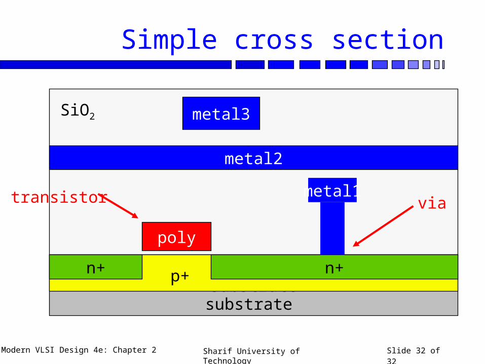
Simple cross section
substraten+ n+p+
substrate
metal1
poly
SiO2
metal2
metal3
transistor via
Modern VLSI Design 4e: Chapter 2 Sharif University of Technology Slide 33 of 32
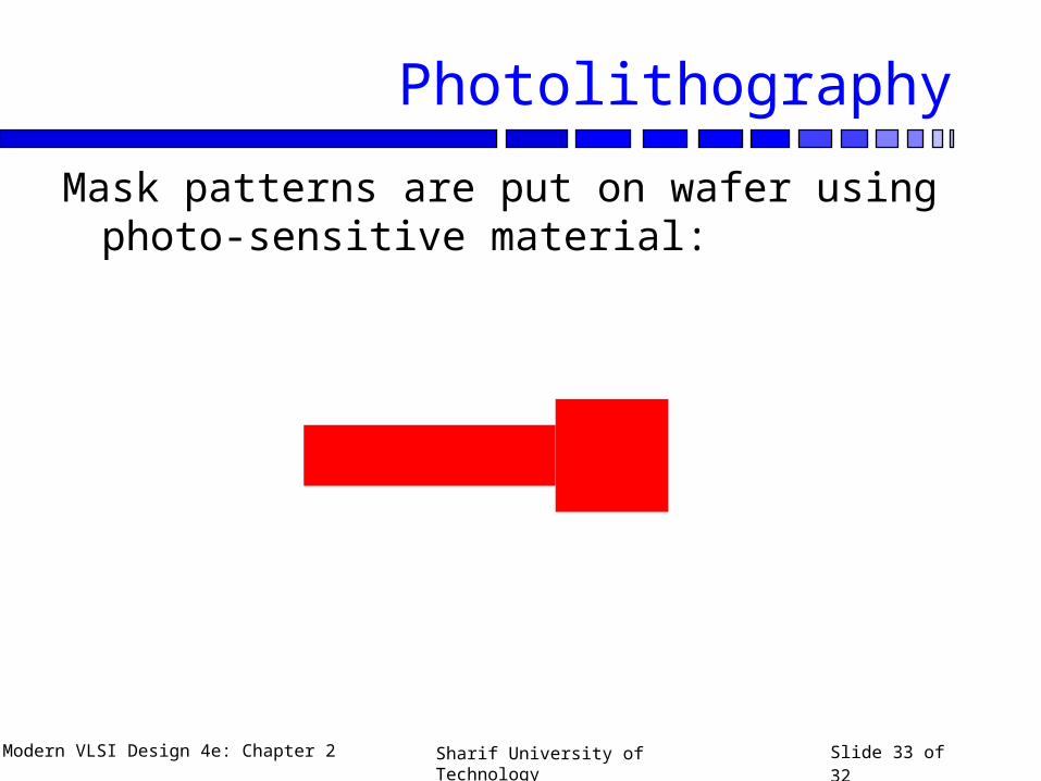
Photolithography
Mask patterns are put on wafer using photo-sensitive material:
Modern VLSI Design 4e: Chapter 2 Sharif University of Technology Slide 34 of 32
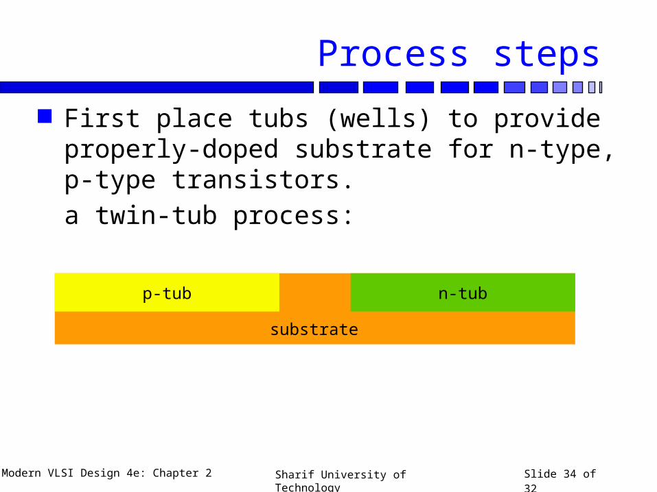
Process steps
First place tubs (wells) to provide properly-doped substrate for n-type, p-type transistors.
a twin-tub process:
p-tub n-tub
substrate
Modern VLSI Design 4e: Chapter 2 Sharif University of Technology Slide 35 of 32
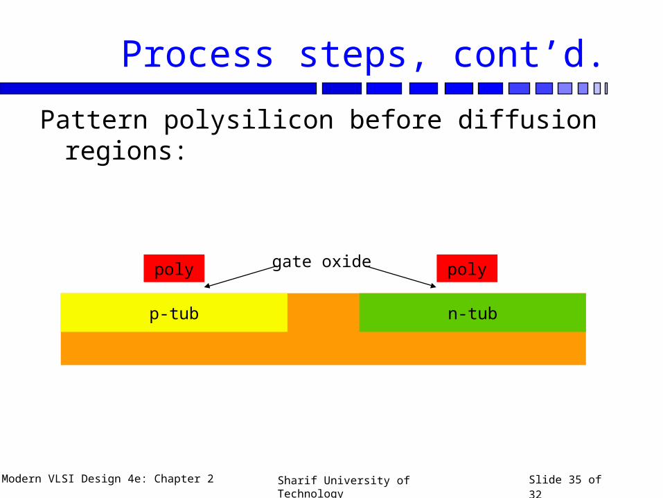
Process steps, cont’d.
Pattern polysilicon before diffusion regions:
p-tub n-tub
poly polygate oxide
Modern VLSI Design 4e: Chapter 2 Sharif University of Technology Slide 36 of 32
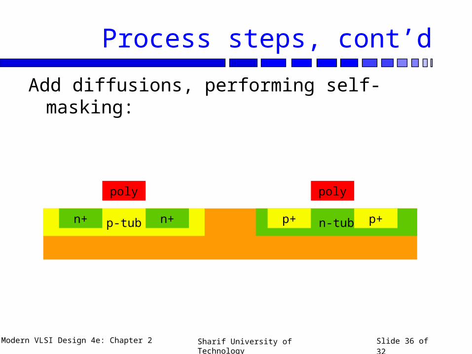
Process steps, cont’d
Add diffusions, performing self-masking:
p-tub n-tub
poly poly
n+n+ p+ p+

Modern VLSI Design 4e: Chapter 2 Sharif University of Technology Slide 37 of 32
Process steps, cont’d
Start adding metal layers:
p-tub n-tub
poly poly
n+n+ p+ p+
metal 1 metal 1
vias
Top Related