


Languages
Pages
Legal


ENERGY MANAGEMENT SYSTEM
NURAINI BINTI AHMAD ARIFF SHAH
This thesis is submitted as partial fulfillment of the requirement for the award
of the degree of Bachelor of Electrical Engineering (Electronics)
Faculty of Electrical & Electronics Engineering
University Malaysia Pahang
APRIL 2009

ii
“I hereby acknowledge that the scope and quality of this thesis is qualified for the award
of the degree of Bachelor of Electrical Engineering (Electronics)”
Signature : ______________________________________________
Name : EN. MOHD SHAWAL BIN JADIN
Date : 23 APRIL 2009

iii
“All the trademark and copyrights use here in are property of their respective owner. References of information from other sources are quoted accordingly; otherwise the information presented in this report is solely work of the author.”
Signature : ____________________________
Author : NURAINI BINTI AHMAD ARIFF SHAH
Date : 23 APRIL 2009

iv
DEDICATION
Specially dedicated to
My beloved parents, lecturer,
and all of my best friends.

v
ACKNOWLEDGEMENTS I am greatly indebted to my supervisor, En Mohd Shawal bin Jadin for providing
me with technical help and overall guidance with the design process. His dedication and
motivation proved to be extremely encouraging throughout the project. I also would like
to thank our FKEE staffs in selecting and ordering parts as well as their technical
guidance throughout the project and helping me to complete my project with the
implementation of the ADE board’s. Suggestions and criticisms from my friends also
have always been helpful in finding solutions to my problems for providing the concept
for the project. I would like to extend mine appreciate to my parent member for giving
me their loves and supports throughout my study in University Malaysia Pahang.
Without the combined effort of the people those who involves directly or indirectly in
completion of my project as mentioned above, this thesis project would not have been
possible.

vi
ABSTRACT
This project report describes the design and implementation of the computer
system Home Energy Management System. The system provides a user the ability to
differentiate between and limit the use of major power consuming appliances, allowing
them to save energy and monitoring power usage at home. This system is developed to
manage the power consumption in daily life. By creating this system the power usage
will be consume wisely without any waste. This system control or limited the power
consumption by turn off the electrical appliance when the amounts of power
consumption exceed the limit. The user can set the desired amount of power usage in
daily in order to save power consumption. It also allows the user to see the consumption
rate for difference appliance in their house by monitor power consumption on LCD
display. Buttons are used to select which parameter (voltage. current and power
consumption) to be monitored. The system required three main parts include on
hardware and software which is power source, controlling unit and monitoring system.
The system used as PIC16F877A as a controller and ADE7753 where offer measured
analog voltage and current input. The analog inputs are sample by ADC within the
ADE7753, and their magnitude and phases are used to digitally calculate real, reactive
and complex power in the line.

vii
ABSTRAK
Laporan projek menerangkan berkenaan rekaan dan applikasi system
berkomputer bagi Sistem Pengurusan Tenaga. Sistem ini menyediakan kemudahan utuk
pengguna bagi membezakan diantara kawalan serta penggunaan kuasa eletrik dimana
membantu pengguna menguruskan penggunaan elektrik dengan cermat.Dengan adanya
system ini penggunaan elektrik akan lebih terkawal tanpa ada pembaziran
berlaku.Sistem ini beroperasi dengan cara mengawal atau menghadkan penggunaan
elektrik sekiranya penggunaan elektrik melebihi had yang ditetapkan.Kadar kawalan
penggunaan elektrik ini boleh ditentukan oleh penguna itu sendiri.Pengguna juga boleh
melihat atau memerhatikan kadar penggunaan elektrik bagi setiap perkakas elektrik di
paparan skrin.Parameter seperti voltan, arus serta penggunaan kuasa boleh juga
dipaparkan di skrin dengan menekan suis butang.Sistem ini terbahagi kepada tiga
bahagian termasuk litar dan program elektrik seperti sumber kuasa, unit kawalan dan
sistem paparan.Sistem ini menggunakan mikro cip PIC16F877A sebagai kawalan dan
ADE7753 dimana menyediakan utuk pengukuran kemasukan analog voltan dan
arus.Kemasukan analog dijadikan sebagai bahan utuk ADC (penukaran bentuk analog
kepada system digital) didalam ADE7753 dan keluaran magnitude dan fasa daripada
hasil tersebut digunakan utk pengiraan kuasa.

viii
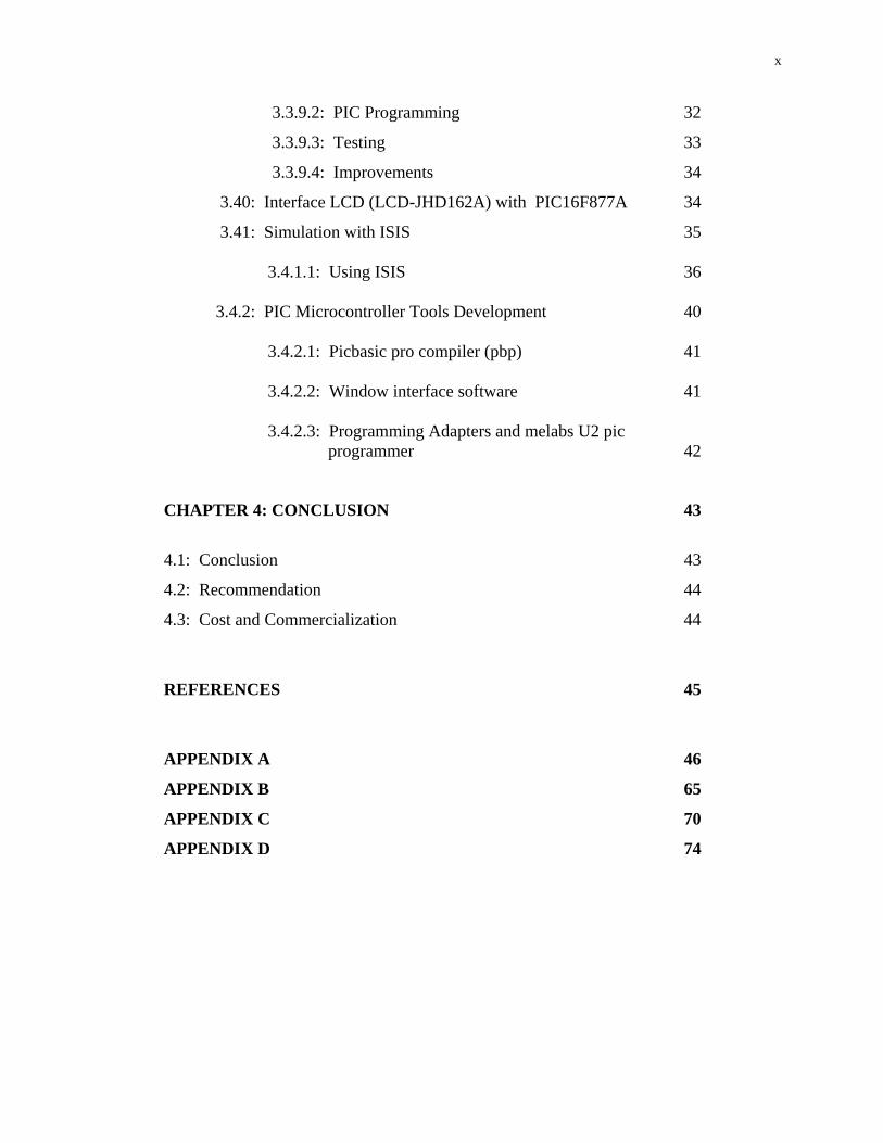
TABLE OF CONTENTS
TITLE PAGE
TITLE PAGE i
DECLARATION ii
DEDICATION iv
ACKNOWLEDGEMENT v
ABSTRACT vi
ABSTRAK vii
TABLE OF CONTENTS viii
LIST OF FIGURES xi
LIST OF TABLES xiii
LIST OF ABBREVIATIONS xiv
LIST OF APPENDIXES xvi
CHAPTER 1: INTRODUCTION 1
1.1 : Introduction 1
1.2 : Research Problem 2
1.3 : Objective 3
1.4 : Scope of Project 3

ix
CHAPTER 2: LITERATURE REVIEW 4
2.1: Introduction 4
2.2: Component review 5
2.2.1: ADE7753 Chip 7
2.2.2: Microchip PIC 16F877A 7
2.2.2.1: Crystal operation 8
2.2.2.2: Reset circuit 9
2.2.2.3: I/O circuit 11
2.2.3: Liquid Crystal Display (LCD) 13 2.2.4: Optocoupler 16 2.2.5: Serial Peripheral Interface Protocol. 18 CHAPTER 3: METHODOLOGY 20
3.1: Introduction 20
3.2: Hardware Design 22
3.3: Block Description 22
3.3.1: Load 22
3.3.2: Power Supply Circuit 22
3.3.3: Energy Measurement Circuit 23
3.3.4: Microcontroller 26
3.3.5: Data Display 28
3.3.6: Interfacing Circuit for Energy Management System 28
3.3.6.1: PIC-ADE Serial Interface 28
3.3.6.2: ADE7753 Serial Communication 28
3.3.6.3: PIC Microprocessor. 30
3.3.7: Relay 30
3.3.8: Optocoupler 30
3.3.9: Implementation 31
3.3.9.1: Serial Communication Implementation 31
x
3.3.9.2: PIC Programming 32
3.3.9.3: Testing 33
3.3.9.4: Improvements 34
3.40: Interface LCD (LCD-JHD162A) with PIC16F877A 34
3.41: Simulation with ISIS 35
3.4.1.1: Using ISIS 36
3.4.2: PIC Microcontroller Tools Development 40 3.4.2.1: Picbasic pro compiler (pbp) 41 3.4.2.2: Window interface software 41 3.4.2.3: Programming Adapters and melabs U2 pic
programmer 42 CHAPTER 4: CONCLUSION 43
4.1: Conclusion 43
4.2: Recommendation 44
4.3: Cost and Commercialization 44
REFERENCES 45
APPENDIX A 46
APPENDIX B 65
APPENDIX C 70
APPENDIX D 74
xi
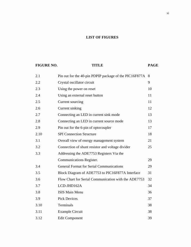
LIST OF FIGURES
FIGURE NO. TITLE PAGE
2.1 Pin out for the 40-pin PDPIP package of the PIC16F877A 8
2.2 Crystal oscillator circuit 9
2.3 Using the power on reset 10
2.4 Using an external reset button 11
2.5 Current sourcing 11
2.6 Current sinking 12
2.7 Connecting an LED in current sink mode 13
2.8 Connecting an LED in current source mode 13
2.9 Pin out for the 6-pin of optocoupler 17
2.10 SPI Connection Structure 18
3.1 Overall view of energy management system 21
3.2 Connection of shunt resistor and voltage divider 25
3.3 Addressing the ADE7753 Registers Via the
Communications Register. 29
3.4 General Format for Serial Communications 29
3.5 Block Diagram of ADE7753 to PIC16F877A Interface 31
3.6 Flow Chart for Serial Communication with the ADE7753 32
3.7 LCD-JHD162A 34
3.8 ISIS Main Menu 36
3.9 Pick Devices 37
3.10 Terminals 38
3.11 Example Circuit 38
3.12 Edit Component 39

xii
3.13 Working Simulation 40
3.14 MicroCode Studio screenshots 42
3.15 Melabs U2 PIC programmer (black chasing) and
programming adapter. 42
xiii
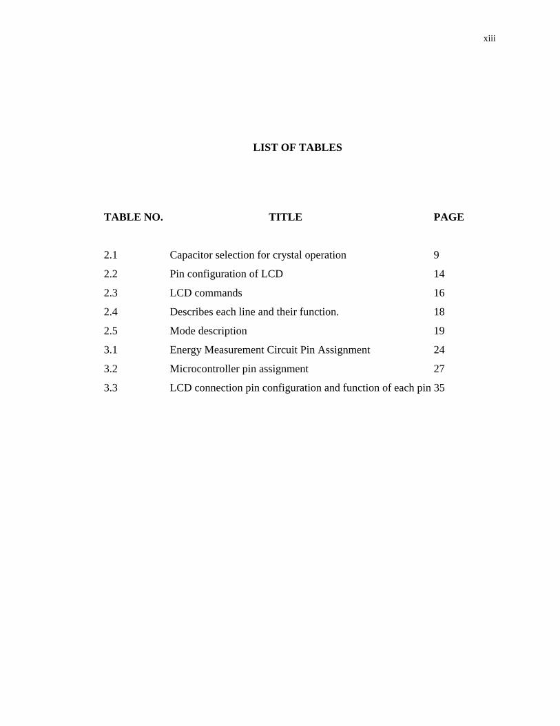
LIST OF TABLES
TABLE NO. TITLE PAGE
2.1 Capacitor selection for crystal operation 9
2.2 Pin configuration of LCD 14
2.3 LCD commands 16
2.4 Describes each line and their function. 18
2.5 Mode description 19
3.1 Energy Measurement Circuit Pin Assignment 24
3.2 Microcontroller pin assignment 27
3.3 LCD connection pin configuration and function of each pin 35
xiv
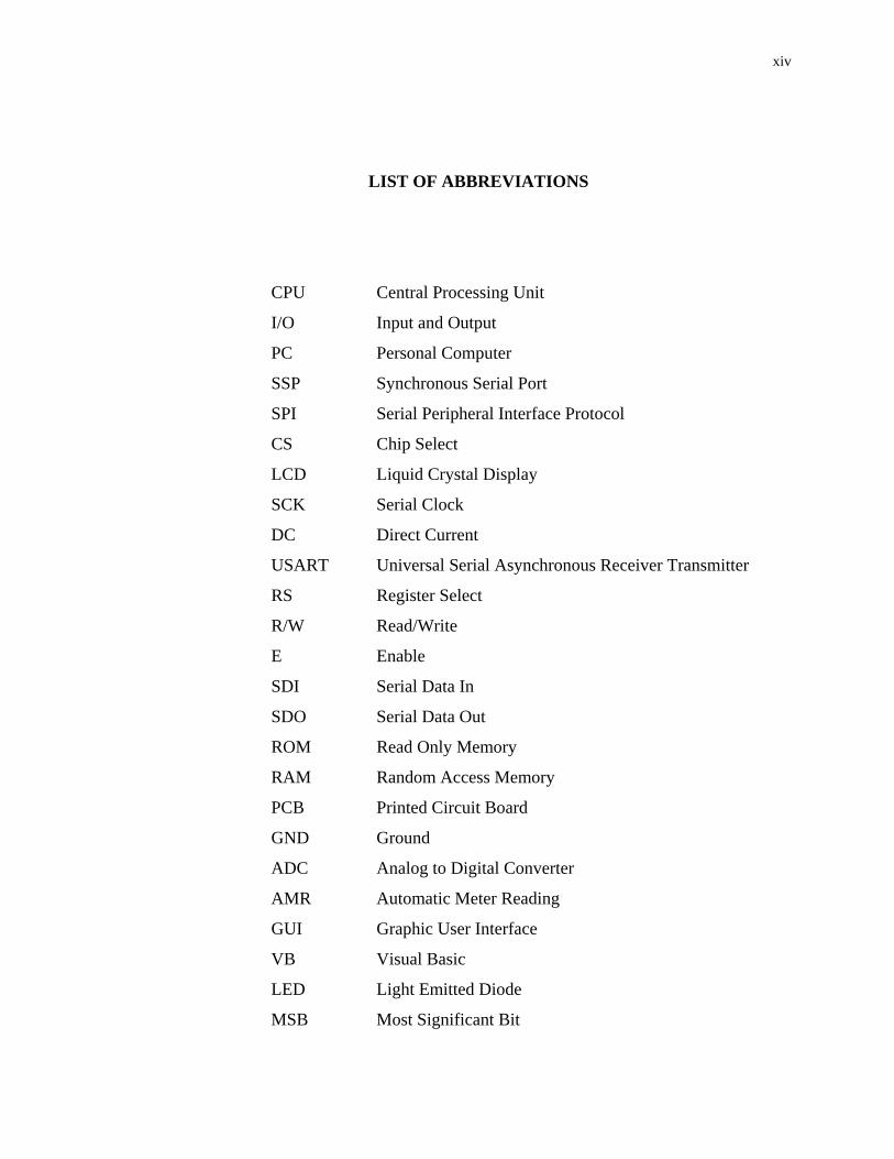
LIST OF ABBREVIATIONS
CPU Central Processing Unit
I/O Input and Output
PC Personal Computer
SSP Synchronous Serial Port
SPI Serial Peripheral Interface Protocol
CS Chip Select
LCD Liquid Crystal Display
SCK Serial Clock
DC Direct Current
USART Universal Serial Asynchronous Receiver Transmitter
RS Register Select
R/W Read/Write
E Enable
SDI Serial Data In
SDO Serial Data Out
ROM Read Only Memory
RAM Random Access Memory
PCB Printed Circuit Board
GND Ground
ADC Analog to Digital Converter
AMR Automatic Meter Reading
GUI Graphic User Interface
VB Visual Basic
LED Light Emitted Diode
MSB Most Significant Bit

xv
LSB Least Significant Bit
EMF Electromagnetic Fields
PBP PicBasic Pro compilers
IDE Integrated Development Environment
ICD In Circuit Debugging

xvi
LIST OF APPENDIXES
APPENDIX NO. TITLE PAGE
A Data Sheets 46
B Schematic Circuit Diagram 65
C Testing Circuit and Program 70
D List of Components 74
1
CHAPTER 1
INTRODUCTION 1.1 Introduction
Energy Management System can also refer to a computer system which is
designed specifically for the automated control and monitoring power usage at home.
This system is developing to manage the power consumption in daily life. By creating
this system the power usage will be consume wisely without any waste. This system
control or limited the power consumption by turn off the electrical appliance when the
amounts of power consumption exceed the limit. It also allows the user to see the
consumption rate for difference appliance in their house by monitor power dissipation
on LCD display and Personal Computer (PC).However the PC only receive the
measured value of current and voltage, then user can interface with PC to determine the
set point to be sent to the microcontroller. In doing this, user definitely can disable
certain appliance when total power consumption is exceed the limit.
By using this system, the user can set the desired amount of power usage in
daily in order to save power consumption. Besides that, user could find the suitable
range of time to use the appliance which is consuming major power will cause the
higher amount of power dissipation. The system also can manipulated the electrical
appliance with automatically or manually turn on and off. This system will be expect to

2
become an intelligent management where it such a good way to save the usage of
power consumption in daily life.
The system required three main parts include on hardware and software which
is power source, controlling unit and monitoring system. The system used a
PIC16F877A as a controller. Basically, this project is designed to be interface with
home electrical appliance based on development of Graphical User Interface (GUI) in
Visual Basic 6.0.For advances features of this system the control unit will able to stand-
alone running or work independently base on the program that been set in control unit
to be automatically react to the data such in order to manipulate the energy
consumption patterns without connected to the PC. This is important causes the usage
of PC 24 hours will draw a lot of power that will affect on this system and bad effect to
our self.
1.2 Research Problem
Rising electricity prices have made it worthwhile for consumers to be informed
about the costs of operating their appliances. All types of consumers of electricity, from
landlords to office managers to the simple home user, are seeking more and more
information about the power consumption of their appliances and electronics in an
effort to reduce power usage and save money. It can be difficult to obtain power
consumption data for most appliances and electronics, and consumers often aren’t sure
of the best ways in which to reduce power consumption. For years, large-scale industry
has spent millions of dollars on equipment and services in an effort to reduce its power
consumption, but there is little such practical and affordable help available to home and
small office consumers.

3
1.3 Objective
The higher goals were to not only build a cheaper, more accurate and more
functional device, but also provide some means by which the characterization of a load
could help save power. To achieve this aim, the study is carried out for the following
objectives.
i. To develop a system function to be as meter for current, voltage and power
reading and also function as an automatic meter reading which is calculated the
amount of power usage especially for management of various load at home.
ii. To develop system where control the appliance by turn on and off automatically
through a PC where the system able to work independently base on program
that has been set in control unit to manipulate the electrical appliance.
1.4 Scope of Project
i. To develop energy management system that view measurement of voltage
(rms), current (rms) and power consumption on LCD display and using
PIC16877A as a controller for this system.
ii. To integrate the hardware and software in order to develop an energy
management system by interfacing of electrical appliance
iii. Develop Graphical User Interface (GUI) using Visual Basic for hardware and
software interfacing.

4
CHAPTER 2
LITERATURE REVIEW
2.1 Introduction
In various countries, there are presently attempts to replace electro-mechanical
power meters with electronic ones. Although the module described in this article was
not specifically designed for that purpose, it can be used as a low cost electronic power
meter module for simple domestic electric power measurement applications. Some of
its advantages over conventional systems are life expectancy and accuracy and the
possibility of remote monitoring [1]
The circuit system is implemented with a power measurement IC (ADE7753)
from Analog Devices. It is capable of measuring instantaneous voltage, current, and
power, VRMSI,m s, and real. Reactive and apparent energy. The interface to the mains
of a site is accomplished using a novel, non-intrusive flexible Rogowski coil developed
as the current sensor. [2]
The ADE7753 is a highly accurate energy metering integrated circuit. It has the
ability to calculate active, reactive and apparent energy. This chip can communicate via
serial data transfer and has a pulse output frequency proportional to the active power
measured. [7]
5
“LCD is used because it consumes less power than seven segment display. It is
responsible for cycling through various modes as commanded by the user in order to
display various power consumption data". [8]
The PIC16F877A was chosen for its SPI mode synchronous serial communication and
large number of general I/O pins available. [7]
2.2 Component review
This section provides the necessary background information required for a
proper understanding of the content discussed in this paper. This includes:
2.2.1 ADE7753 Chip
In this project, ADE7753 IC chip from Analog Devices are used for measuring
electric appliance. This chip is based on an inexpensive shunt resistor.
2.2.2 Microchip PIC 16F877A
The Microcontroller primarily performs the function of converting the analog
signal inputs into an 8 bit digital value. It performs basic measurements on the
waveforms to obtain the average power and displays this on a 2 x 16, on green LCD
display. To use a microcontroller in this project, all operation as states below are should
be know.
2.2.2.1 Crystal operation
These circuits are used as a clock input for microcontroller to control the
internal clock generator circuitry.

6
2.2.2.2 Reset circuit
This circuit is used as an input to initialize the PIC16F877A to a know start up
state.
2.2.2.3 I/O circuit
In microcontroller, the input and output device are needed for develop system
function. This section will describe in detail about the input and output circuit.
2.2.3 Liquid Crystal Display (LCD)
In this section described LCD as a monitoring system in develop this project.
2.2.4 Optocoupler
Describe the function of this device as an isolation using in Energy
Management System.
2.2.5 Serial Peripheral Interface Protocol.
This topic will describe the way to communicate with one or more slave devices.
7
2.2.1 ADE7753 Chip
The ADE7753 is a highly accurate energy metering integrated circuit. It has the
ability to calculate active, reactive, and apparent energy. This chip can communicate
via serial data transfer and has a pulse output frequency proportional to the active
power measured. This chip requires analog inputs of voltage and current applied to its
input terminals. The maximum differential signal level is ± .5 volts with respect to
AGND. The gain of both of these channels can be changed to account for error in the
transformers. There is a selectable on-chip digital integrator which can provide an
interface to a current sensor like a Rogowski coil. The analog to digital conversion in
the ADE7753 is achieved by using two second-order Σ-Δ ADCs. The sampling rate is
determined by the sampling clock which is equal to the input clock divided by four.
There are many system calibration features in this chip including channel offset
correction, phase calibration, and power calibration. This allows it to provide very
accurate power information. The ADE7753 power measurement chip met all our
operating specifications. This chip is capable of measuring single phase power with
several built in calibration points for precise power measurement. The chip
communicates via serial communication which can be easily integrated with a PIC
microprocessor. The chip has 24 bit internal registers which are used to accumulate the
power measured. This data can be read using a serial peripheral interface with the chip
2.2.2 Microchip PIC 16F877A
The Microchip PIC16F877A is an inexpensive 8-bit microcontroller. Its features
include 256 bytes of EEPROM data memory, self programming, two Comparators,
eight channels of 10-bit Analog-to-Digital (A/D) converter, a Synchronous Serial Port
(SSP), a Universal Serial Asynchronous Receiver Transmitter (USART), and three
separate timer modules. It contains 14.3KB worth of program memory and is capable of
operating with up to a 20MHz clock (200ns instruction cycle). The primary
functionality for the PIC in the EMS is to perform a serial read on the active energy

8
register on the ADE chip. Secondary functions include turning the EMS on and off. The
PIC16F877A was chosen for its SPI mode synchronous serial communication and large
number of general I/O pins available.
Figure 2.1: Pin out for the 40-pin PDPIP package of the PIC16F877A
2.2.2.1 Crystal operation
As shown in Figure 2.2, in this mode of operation an external crystal and two
capacitors are connected to the OSC1 and OSC2 inputs of the microcontroller. The
capacitors should be chosen as in Table 2.1. For example, with a crystal frequency of 4
MHz, two 22 pF capacitors can be used

9
Figure 2.2 Crystal oscillator circuit
Table 2.1: Capacitor selection for crystal operation
2.2.2.2 Reset circuit
Reset is used to put the microcontroller into a known state. Normally when a
PIC microcontroller is reset execution starts from address 0 of the program memory.
This is where the first executable user program resides. The reset action also initializes
various SFR registers inside the microcontroller. PIC microcontrollers can be reset
when one of the following conditions occur:
10
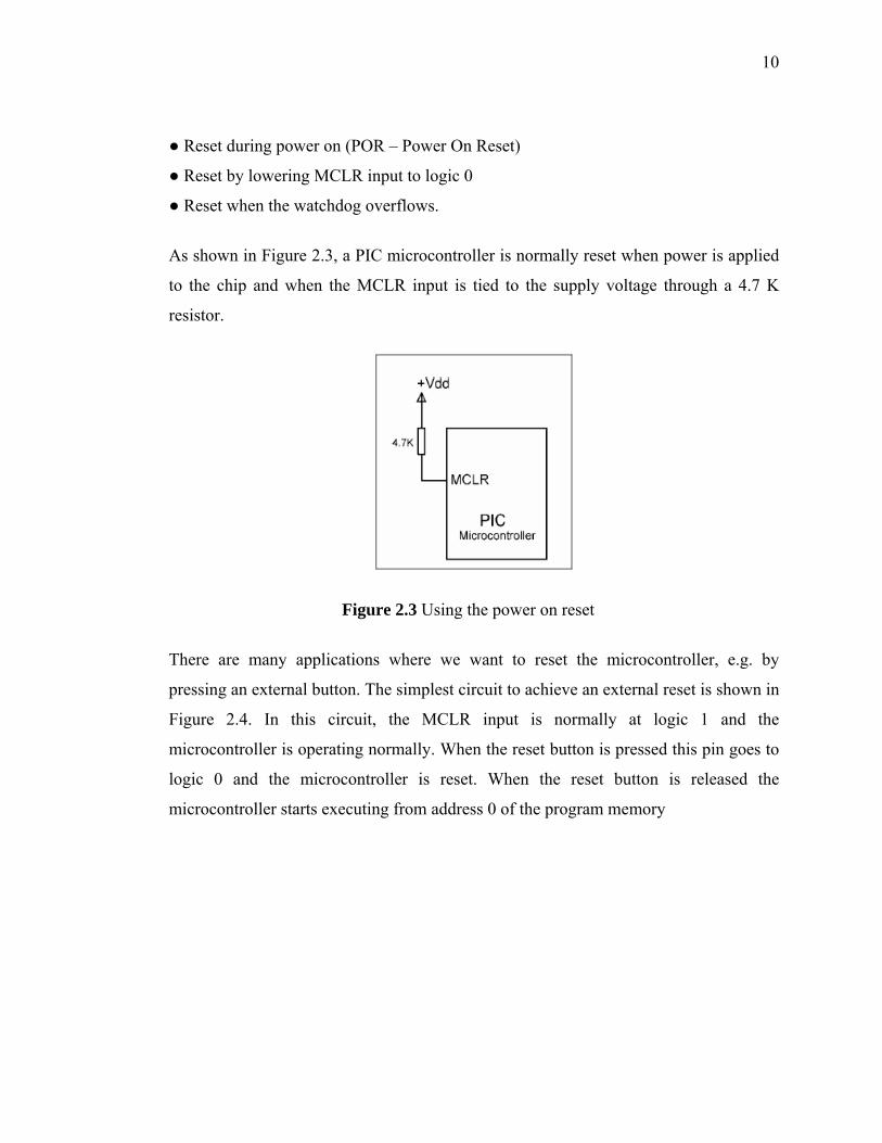
● Reset during power on (POR – Power On Reset)
● Reset by lowering MCLR input to logic 0
● Reset when the watchdog overflows.
As shown in Figure 2.3, a PIC microcontroller is normally reset when power is applied
to the chip and when the MCLR input is tied to the supply voltage through a 4.7 K
resistor.
Figure 2.3 Using the power on reset
There are many applications where we want to reset the microcontroller, e.g. by
pressing an external button. The simplest circuit to achieve an external reset is shown in
Figure 2.4. In this circuit, the MCLR input is normally at logic 1 and the
microcontroller is operating normally. When the reset button is pressed this pin goes to
logic 0 and the microcontroller is reset. When the reset button is released the
microcontroller starts executing from address 0 of the program memory

11
Figure 2.4: Using an external reset button
2.2.2.3 I/O circuit
A PIC microcontroller port can source and sink 25 mA of current. When
sourcing current, the current is flowing out of the port pin, and when sinking current,
the current is flowing into the pin. When the pin is sourcing current, one pin of the load
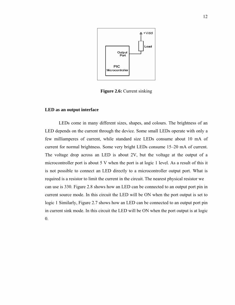
is connected to the microcontroller port and the other pin to the ground (see Figure 2.5).
The load is then energized when the port output is at logic 1. When the pin is sinking
current, one pin of the load is connected to the supply voltage and the other pin to the
output of the port (see Figure 2.6). The load is then energized when the port output is at
logic 0.
Figure 2.5: Current sourcing
12
Figure 2.6: Current sinking
LED as an output interface
LEDs come in many different sizes, shapes, and colours. The brightness of an
LED depends on the current through the device. Some small LEDs operate with only a
few milliamperes of current, while standard size LEDs consume about 10 mA of
current for normal brightness. Some very bright LEDs consume 15–20 mA of current.
The voltage drop across an LED is about 2V, but the voltage at the output of a
microcontroller port is about 5 V when the port is at logic 1 level. As a result of this it
is not possible to connect an LED directly to a microcontroller output port. What is
required is a resistor to limit the current in the circuit. The nearest physical resistor we
can use is 330. Figure 2.8 shows how an LED can be connected to an output port pin in
current source mode. In this circuit the LED will be ON when the port output is set to
logic 1 Similarly, Figure 2.7 shows how an LED can be connected to an output port pin
in current sink mode. In this circuit the LED will be ON when the port output is at logic
0.

13
Figure 2.7 Connecting an LED in current sink mode
Figure 2.8 Connecting an LED in current source mode
2.2.3 Liquid Crystal Display (LCD)
In many microcontroller-based applications, it is required to display a message
or the value of a variable. Basically, three types of displays can be used in practice.
These are video displays, 7-segment LED displays, and LCD displays. For this project
LCD are used for display purpose. LCDs are alphanumeric displays which are
frequently used in microcontroller-based applications. Some of the advantages of LCDs
are their low cost and low power consumption. LCDs are ideal in low-power, battery-
operated portable applications. These displays come in different shapes and sizes. In
14
this section, are looking at how interfacing for the standard LCDs to a PIC
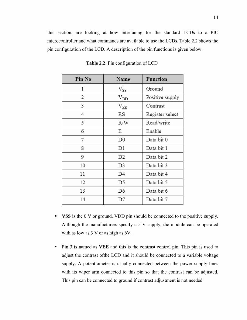
microcontroller and what commands are available to use the LCDs. Table 2.2 shows the
pin configuration of the LCD. A description of the pin functions is given below.
Table 2.2: Pin configuration of LCD
VSS is the 0 V or ground. VDD pin should be connected to the positive supply.
Although the manufacturers specify a 5 V supply, the module can be operated
with as low as 3 V or as high as 6V.
Pin 3 is named as VEE and this is the contrast control pin. This pin is used to
adjust the contrast ofthe LCD and it should be connected to a variable voltage
supply. A potentiometer is usually connected between the power supply lines
with its wiper arm connected to this pin so that the contrast can be adjusted.
This pin can be connected to ground if contrast adjustment is not needed.
15
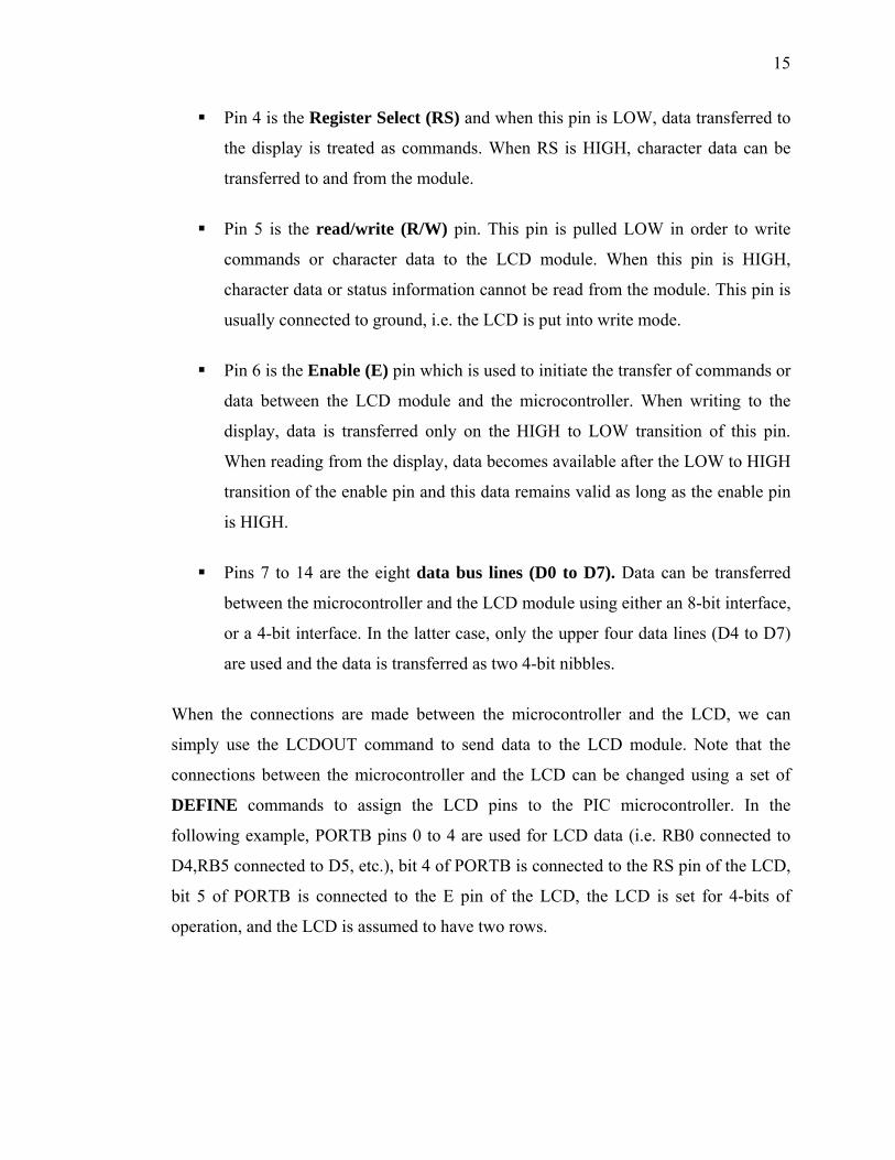
Pin 4 is the Register Select (RS) and when this pin is LOW, data transferred to
the display is treated as commands. When RS is HIGH, character data can be
transferred to and from the module.
Pin 5 is the read/write (R/W) pin. This pin is pulled LOW in order to write
commands or character data to the LCD module. When this pin is HIGH,
character data or status information cannot be read from the module. This pin is
usually connected to ground, i.e. the LCD is put into write mode.
Pin 6 is the Enable (E) pin which is used to initiate the transfer of commands or
data between the LCD module and the microcontroller. When writing to the
display, data is transferred only on the HIGH to LOW transition of this pin.
When reading from the display, data becomes available after the LOW to HIGH
transition of the enable pin and this data remains valid as long as the enable pin
is HIGH.
Pins 7 to 14 are the eight data bus lines (D0 to D7). Data can be transferred
between the microcontroller and the LCD module using either an 8-bit interface,
or a 4-bit interface. In the latter case, only the upper four data lines (D4 to D7)
are used and the data is transferred as two 4-bit nibbles.
When the connections are made between the microcontroller and the LCD, we can
simply use the LCDOUT command to send data to the LCD module. Note that the
connections between the microcontroller and the LCD can be changed using a set of
DEFINE commands to assign the LCD pins to the PIC microcontroller. In the
following example, PORTB pins 0 to 4 are used for LCD data (i.e. RB0 connected to
D4,RB5 connected to D5, etc.), bit 4 of PORTB is connected to the RS pin of the LCD,
bit 5 of PORTB is connected to the E pin of the LCD, the LCD is set for 4-bits of
operation, and the LCD is assumed to have two rows.

16
DEFINE LCD_DREG PORTB ‘Set LCD data port to PORTB
DEFINE LCD_DBIT 0 ‘Set data starting bit to 0
DEFINE LCD_RSREG PORTB ‘Set RS register port to PORTB
DEFINE LCD_RSBIT 4 ‘Set RS register bit to 4
DEFINE LCD_EREG PORTB ‘Set E register port
DEFINE LCD_EBIT 5 ‘Set E register bit to 5
DEFINE LCD_BITS 4 ‘Set 4 bit operation
DEFINE LCD_LINES 2 ‘Set number of LCD rows
The character set of the LCD is given in Table 2.3
Table 2.3: LCD commands
2.2.4 Optocoupler
This device is used because the source and destination are at very different
voltage levels, like a microprocessor which is operating from 5V DC but being used to
control an electrical appliance which is switching 240V AC. The link between the two
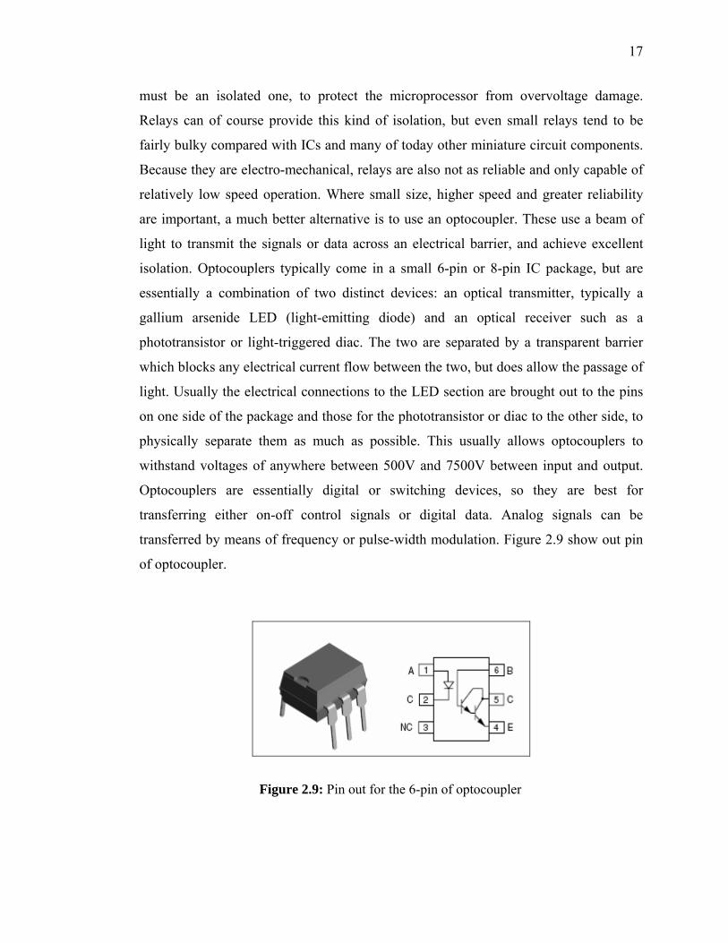
17
must be an isolated one, to protect the microprocessor from overvoltage damage.
Relays can of course provide this kind of isolation, but even small relays tend to be
fairly bulky compared with ICs and many of today other miniature circuit components.
Because they are electro-mechanical, relays are also not as reliable and only capable of
relatively low speed operation. Where small size, higher speed and greater reliability
are important, a much better alternative is to use an optocoupler. These use a beam of
light to transmit the signals or data across an electrical barrier, and achieve excellent
isolation. Optocouplers typically come in a small 6-pin or 8-pin IC package, but are
essentially a combination of two distinct devices: an optical transmitter, typically a
gallium arsenide LED (light-emitting diode) and an optical receiver such as a
phototransistor or light-triggered diac. The two are separated by a transparent barrier
which blocks any electrical current flow between the two, but does allow the passage of
light. Usually the electrical connections to the LED section are brought out to the pins
on one side of the package and those for the phototransistor or diac to the other side, to
physically separate them as much as possible. This usually allows optocouplers to
withstand voltages of anywhere between 500V and 7500V between input and output.
Optocouplers are essentially digital or switching devices, so they are best for
transferring either on-off control signals or digital data. Analog signals can be
transferred by means of frequency or pulse-width modulation. Figure 2.9 show out pin
of optocoupler.
Figure 2.9: Pin out for the 6-pin of optocoupler
18
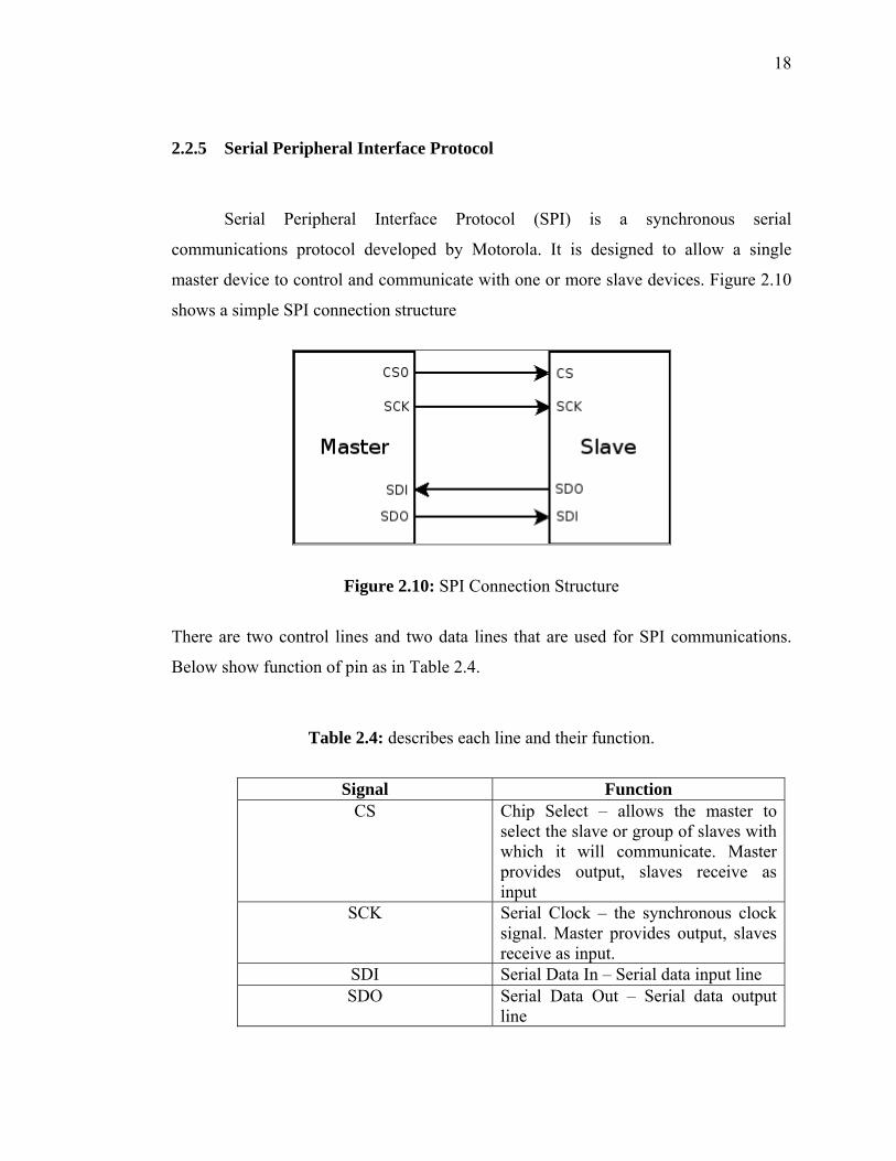
2.2.5 Serial Peripheral Interface Protocol
Serial Peripheral Interface Protocol (SPI) is a synchronous serial
communications protocol developed by Motorola. It is designed to allow a single
master device to control and communicate with one or more slave devices. Figure 2.10
shows a simple SPI connection structure
Figure 2.10: SPI Connection Structure
There are two control lines and two data lines that are used for SPI communications.
Below show function of pin as in Table 2.4.
Table 2.4: describes each line and their function.
Signal Function
CS Chip Select – allows the master to select the slave or group of slaves with which it will communicate. Master provides output, slaves receive as input
SCK Serial Clock – the synchronous clock signal. Master provides output, slaves receive as input.
SDI Serial Data In – Serial data input line SDO Serial Data Out – Serial data output
line
19
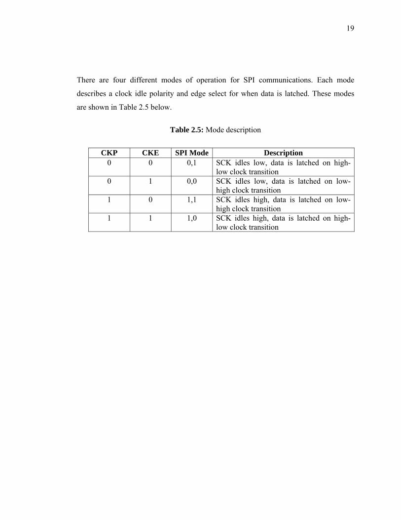
There are four different modes of operation for SPI communications. Each mode
describes a clock idle polarity and edge select for when data is latched. These modes
are shown in Table 2.5 below.
Table 2.5: Mode description
CKP CKE SPI Mode Description
0 0 0,1 SCK idles low, data is latched on high-low clock transition
0 1 0,0 SCK idles low, data is latched on low-high clock transition
1 0 1,1 SCK idles high, data is latched on low-high clock transition
1 1 1,0 SCK idles high, data is latched on high-low clock transition

20
CHAPTER 3
METHODOLOGY
3.1 Introduction
In this chapter, the equipments used, the procedures and the method for the
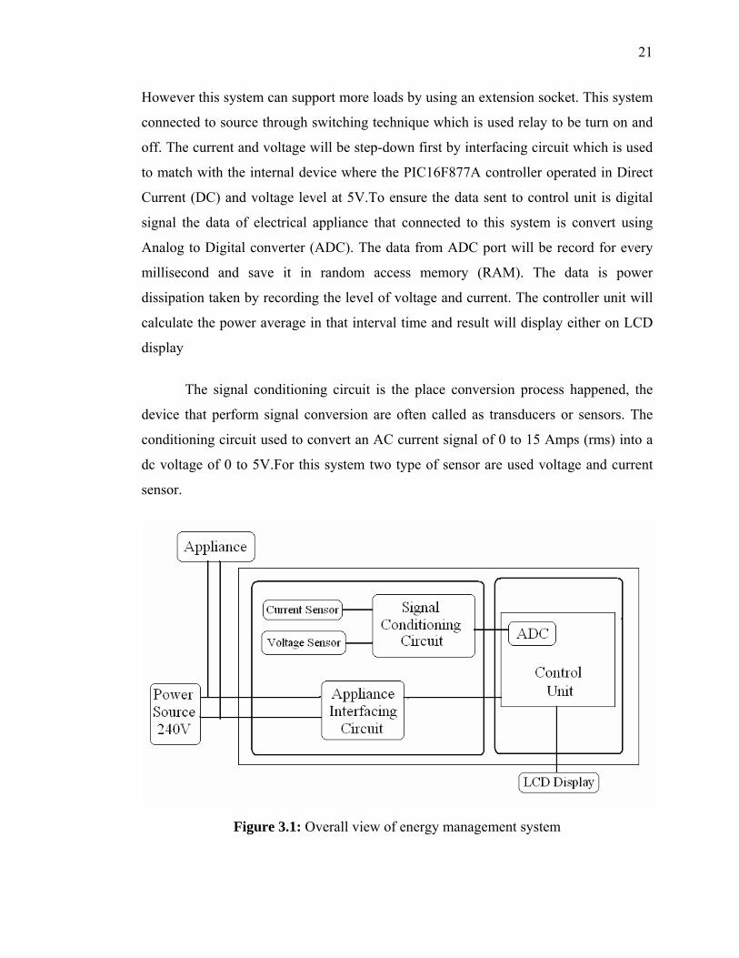
research is discussed. The main study of this chapter is to determine the overall circuit
of the energy management system. The figure 1 has shown the overall system of energy
management system. The system consists three main parts include on hardware and
software which is power source, controlling unit and monitoring system. Controlling
unit is a main of energy management system where control by PIC16F877A.This
controller are choose because of instruction set are simple and seamless migration
between product families make PIC16F877A microcontrollers the logical choice for
designing requiring flexibility and performance. This controller used to execute the
programs that has written or set that is stored in memory. This controller also functions
to record and save the data in random access memory (RAM) and calculate the power
average used of each appliance that connected to the system.
This system running in condition stand-alone running (without connected to the
PC).. In overall this system is operated when the load (electrical appliance) is connected
to the power source 240 Vrms, 50Hz. This system only operated in single phase source.
21
However this system can support more loads by using an extension socket. This system
connected to source through switching technique which is used relay to be turn on and
off. The current and voltage will be step-down first by interfacing circuit which is used
to match with the internal device where the PIC16F877A controller operated in Direct
Current (DC) and voltage level at 5V.To ensure the data sent to control unit is digital
signal the data of electrical appliance that connected to this system is convert using
Analog to Digital converter (ADC). The data from ADC port will be record for every
millisecond and save it in random access memory (RAM). The data is power
dissipation taken by recording the level of voltage and current. The controller unit will
calculate the power average in that interval time and result will display either on LCD
display
The signal conditioning circuit is the place conversion process happened, the
device that perform signal conversion are often called as transducers or sensors. The
conditioning circuit used to convert an AC current signal of 0 to 15 Amps (rms) into a
dc voltage of 0 to 5V.For this system two type of sensor are used voltage and current
sensor.
Figure 3.1: Overall view of energy management system

22
3.2 Hardware Design
The project involves the design, layout, and fabrication of a custom printed circuit
board (PCB). The power consumption meter will be powered from the socket it is
currently measuring and thus requires on-board power conversion hardware. The bulk
of the hardware focuses on power consumption measurement and data storage. Finally,
hardware to display the data and accept user input is also required.
3.3 Block Description
3.3.1 Load
These energy management systems use any house-hold consumer load. The
system investigating various loads with rated power consumptions of around 9 KW
such as water heater, lamp and etc.
3.3.2 Power Supply Circuit
For this circuit utilize an appropriate power supply that converts the 240 V, 50
Hz AC voltage to appropriate DC values (mainly 5 volt, and additionally 12 volts if
required) to power the ADE, PIC, Relay, and LCD circuit. Batteries and adapter also
are looking for providing power for this circuit. The main purpose of power supply
module is to be as power source to the system.
23
3.3.3 Energy Measurement Circuit
The Energy Measurement circuit is responsible for direct current, voltage, and
power angle measurements, and from them, determining real and reactive power
consumption. The Energy Measurement circuit must be capable of relaying these
measured and calculated values to the microcontroller via a serial bus. The heart of the
Energy Measurement subsystem is Analog Devices Energy Meter p/n ADE7753. The
ADE7753 offers analog voltage and current inputs, and an SPI serial interface. Both
voltage and current inputs require a 0 to 0.5V analog input. The analog inputs are
sampled by ADCs within the ADE7753, and their magnitudes and phases are used to
digitally calculate real, reactive, and complex power in the line. The current sensing
circuit consists of a single shunt resistor rated at 0.02 Ohms and 5W.The resistor is
located in the Neutral wire, and is tapped at both sides. The load side is connected to
pin V1P, and the source side is connected to pin V1N. Maximum current to be drawn
through the line is 15A, and so voltage across the current sense resistor will range from
zero to 0.3VAC. Maximum sustained power dissipation in the resistor when 15A is
being drawn will be approximately 4.5W, which is within the resistor s rated operation.
The voltage sensing circuit consists of a high-impedance bridge between the Hot and
Neutral wires. Two high-precision resistors rated at 470k Ohms and 680 Ohms are
connected in series between the Hot and Neutral lines as shown in figure 4.1 Pins V2P
and V2N are connected across the 680 Ohm resistor. Note that at 240VAC line voltage,
the current leakage through the voltage sensing bridge is approximately 0.5mA, and
therefore power dissipation in the voltage sense resistors is not a concern. In Appendix
B shows the circuits diagram of the Energy Measurement system and Table 3.1 below
outlines in detail each pin connection of the device
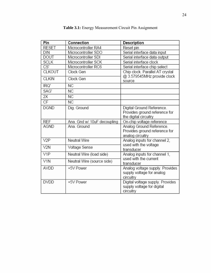
24
Table 3.1: Energy Measurement Circuit Pin Assignment
Top Related