


Languages
Pages
Legal

Trieste, 8-10 November 1999
CMOS technology 1
Outline
• Introduction• CMOS devices• CMOS technology• CMOS logic structures• CMOS sequential circuits• CMOS regular structures
Trieste, 8-10 November 1999
CMOS technology 2
CMOS technology
• Lithography• Physical structure• CMOS fabrication sequence• Yield• Design rules• Other processes• Advanced CMOS process• Process enhancements• Technology scaling
Trieste, 8-10 November 1999
CMOS technology 3
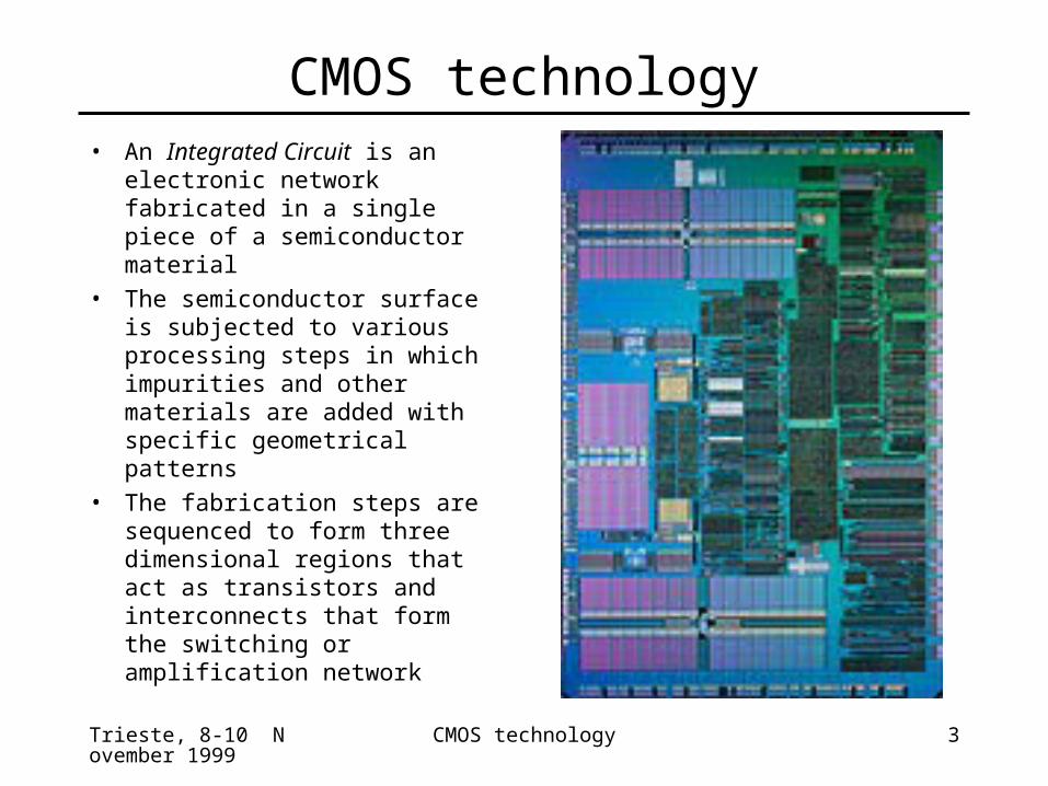
CMOS technology• An Integrated Circuit is an
electronic network fabricated in a single piece of a semiconductor material
• The semiconductor surface is subjected to various processing steps in which impurities and other materials are added with specific geometrical patterns
• The fabrication steps are sequenced to form three dimensional regions that act as transistors and interconnects that form the switching or amplification network
Trieste, 8-10 November 1999
CMOS technology 4
Lithography
Lithography: process used to transfer patterns to each layer of the IC
Lithography sequence steps:• Designer:
– Drawing the layer patterns on a layout editor
• Silicon Foundry:– Masks generation from the layer patterns in the design data
base– Printing: transfer the mask pattern to the wafer surface– Process the wafer to physically pattern each layer of the IC
Trieste, 8-10 November 1999
CMOS technology 5
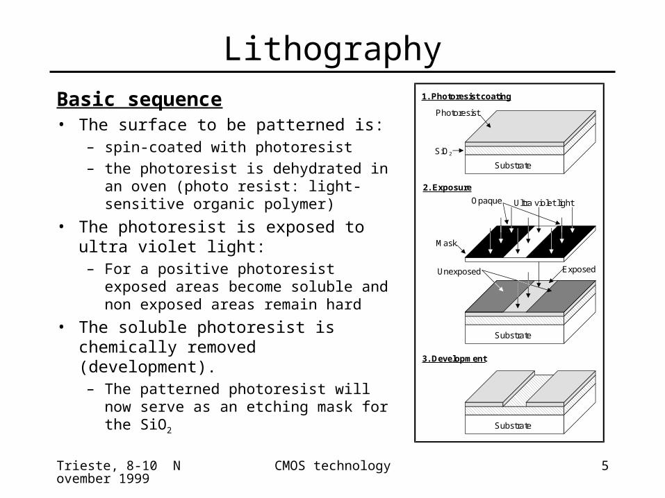
Lithography
Basic sequence• The surface to be patterned is:
– spin-coated with photoresist
– the photoresist is dehydrated in an oven (photo resist: light-sensitive organic polymer)
• The photoresist is exposed to ultra violet light:– For a positive photoresist exposed
areas become soluble and non exposed areas remain hard
• The soluble photoresist is chemically removed (development).– The patterned photoresist will now
serve as an etching mask for the SiO2
1. Photoresist coating
SiO2
Photoresist
Substrate
3. Development
Substrate
Substrate
Mask
Ultra violet lightOpaque
ExposedUnexposed
2. Exposure
Trieste, 8-10 November 1999
CMOS technology 6
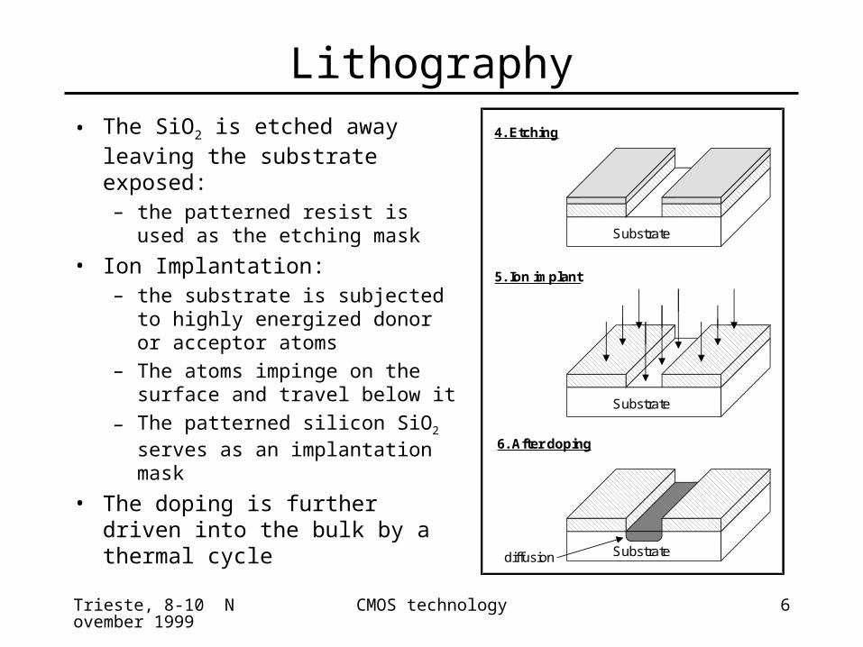
Lithography• The SiO2 is etched away leaving
the substrate exposed:– the patterned resist is used as
the etching mask
• Ion Implantation:– the substrate is subjected to
highly energized donor or acceptor atoms
– The atoms impinge on the surface and travel below it
– The patterned silicon SiO2 serves as an implantation mask
• The doping is further driven into the bulk by a thermal cycle
4. Etching
Substrate
Substrate
5. Ion implant
Substrate
6. After doping
diffusion
Trieste, 8-10 November 1999
CMOS technology 7
Lithography
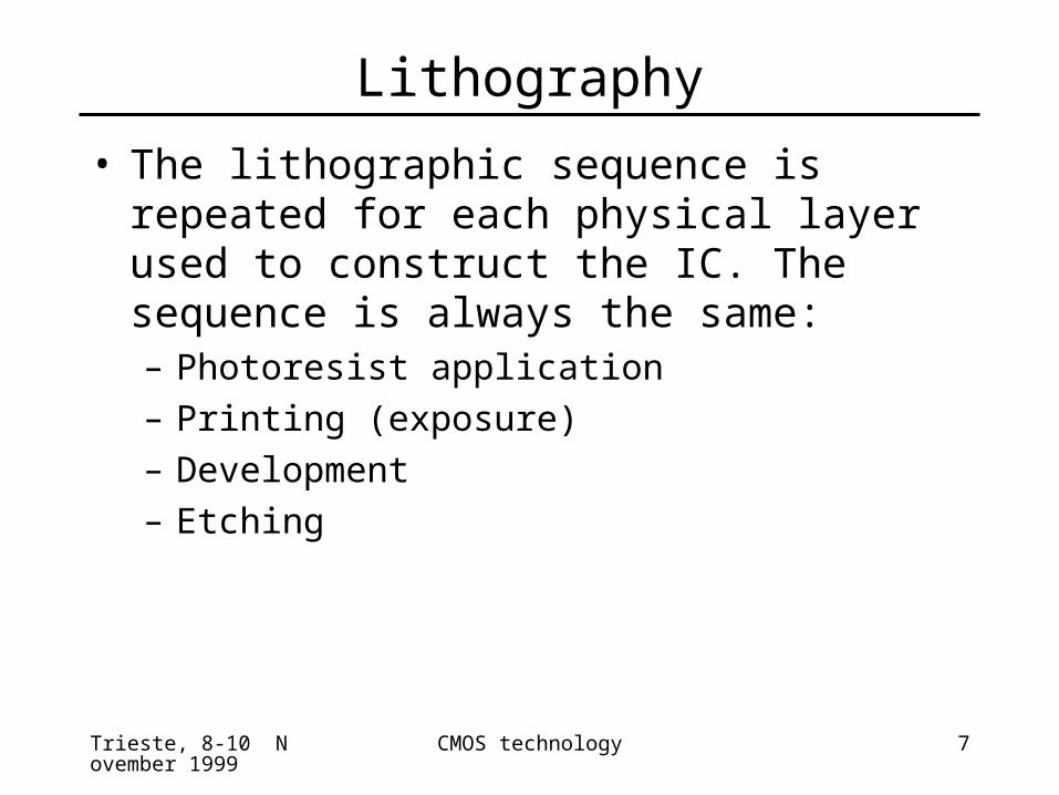
• The lithographic sequence is repeated for each physical layer used to construct the IC. The sequence is always the same:– Photoresist application– Printing (exposure)– Development– Etching
Trieste, 8-10 November 1999
CMOS technology 8
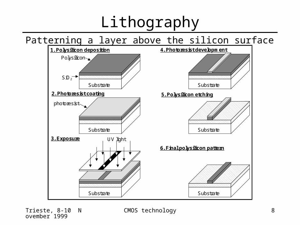
LithographyPatterning a layer above the silicon surface
Substrate
SiO2
Polysilicon
1. Polysilicon deposition
2. Photoresist coating
photoresist
Substrate
Substrate
3. Exposure UV light
Substrate
4. Photoresist development
Substrate
5. Polysilicon etching
Substrate
6. Final polysilicon pattern
Trieste, 8-10 November 1999
CMOS technology 9
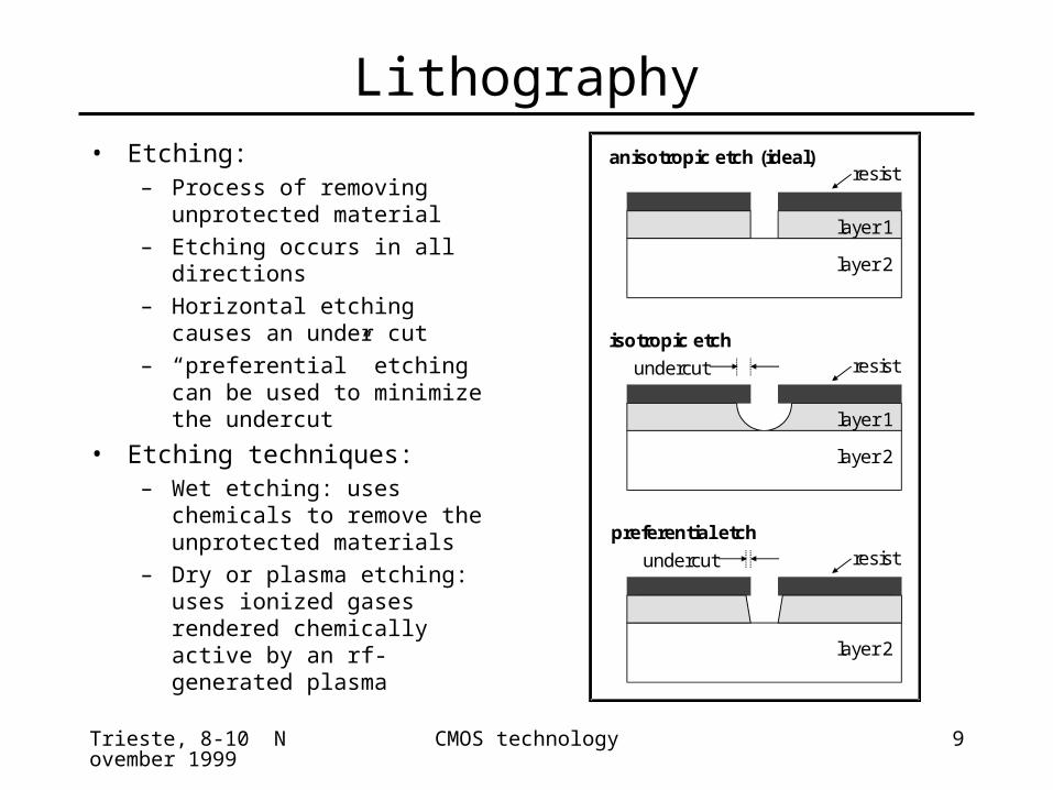
Lithography• Etching:
– Process of removing unprotected material
– Etching occurs in all directions– Horizontal etching causes an
under cut– “preferential” etching can be
used to minimize the undercut
• Etching techniques:– Wet etching: uses chemicals to
remove the unprotected materials
– Dry or plasma etching: uses ionized gases rendered chemically active by an rf-generated plasma
anisotropic etch (ideal)resist
layer 1
layer 2
resist
layer 1
layer 2
isotropic etch
undercut
resist
layer 1
layer 2
preferential etch
undercut
Trieste, 8-10 November 1999
CMOS technology 10
Physical structure
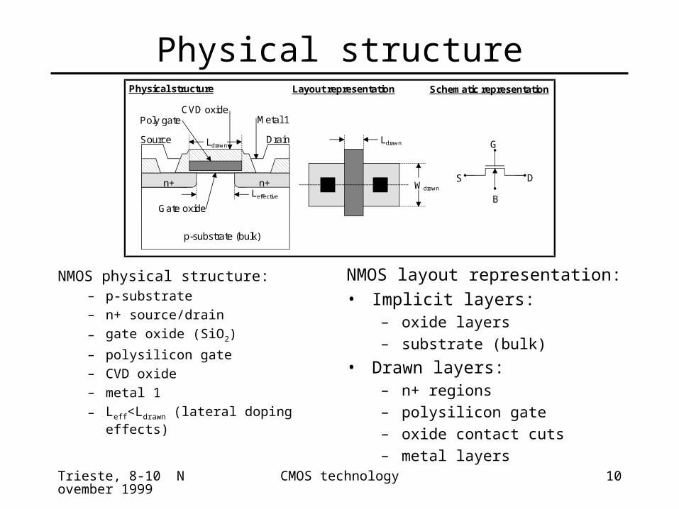
NMOS physical structure:– p-substrate– n+ source/drain
– gate oxide (SiO2)
– polysilicon gate– CVD oxide– metal 1
– Leff<Ldrawn (lateral doping effects)
p-substrate (bulk)
Gate oxide
n+ n+
Ldrawn
Leffective
Source Drain
Poly gate Metal 1CVD oxide
Ldrawn
Wdrawn
Physical structure Layout representation Schematic representation
S D
G
B
NMOS layout representation:
• Implicit layers:– oxide layers– substrate (bulk)
• Drawn layers:– n+ regions– polysilicon gate– oxide contact cuts– metal layers
Trieste, 8-10 November 1999
CMOS technology 11
Physical structure
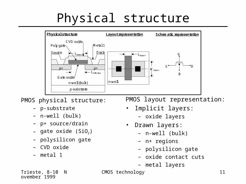
PMOS physical structure:– p-substrate– n-well (bulk)– p+ source/drain
– gate oxide (SiO2)
– polysilicon gate– CVD oxide– metal 1
PMOS layout representation:
• Implicit layers:– oxide layers
• Drawn layers:– n-well (bulk)– n+ regions– polysilicon gate– oxide contact cuts– metal layers
Physical structure Layout representation Schematic representation
p-substrate
Gate oxide
p+ p+
Ldrawn
Leffective
Source Drain
Poly gate Metal 1CVD oxide
n-well (bulk)
Ldrawn
Wdrawn
n-well
S D
G
B
Trieste, 8-10 November 1999
CMOS technology 12
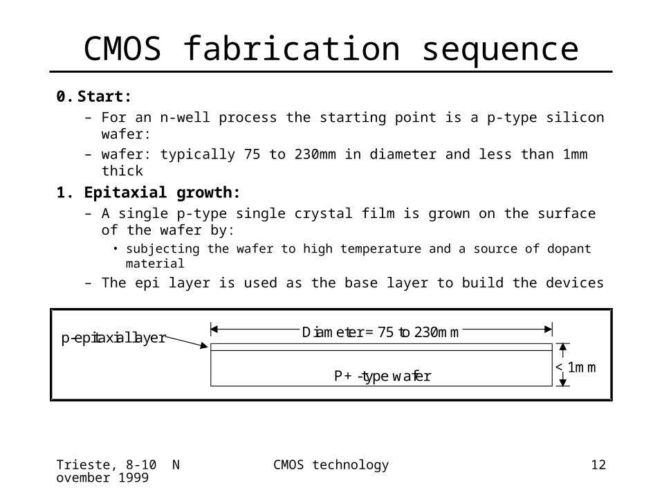
CMOS fabrication sequence0. Start:
– For an n-well process the starting point is a p-type silicon wafer:
– wafer: typically 75 to 230mm in diameter and less than 1mm thick
1. Epitaxial growth:– A single p-type single crystal film is grown on the surface of the
wafer by:• subjecting the wafer to high temperature and a source of dopant
material
– The epi layer is used as the base layer to build the devices
P+ -type wafer
p-epitaxial layer Diameter = 75 to 230mm
< 1mm
Trieste, 8-10 November 1999
CMOS technology 13
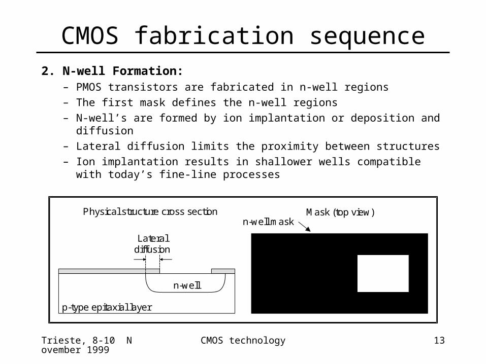
CMOS fabrication sequence2. N-well Formation:
– PMOS transistors are fabricated in n-well regions
– The first mask defines the n-well regions
– N-well’s are formed by ion implantation or deposition and diffusion
– Lateral diffusion limits the proximity between structures
– Ion implantation results in shallower wells compatible with today’s fine-line processes
p-type epitaxial layer
n-well
Lateraldiffusion
Physical structure cross section Mask (top view)n-well mask
Trieste, 8-10 November 1999
CMOS technology 14
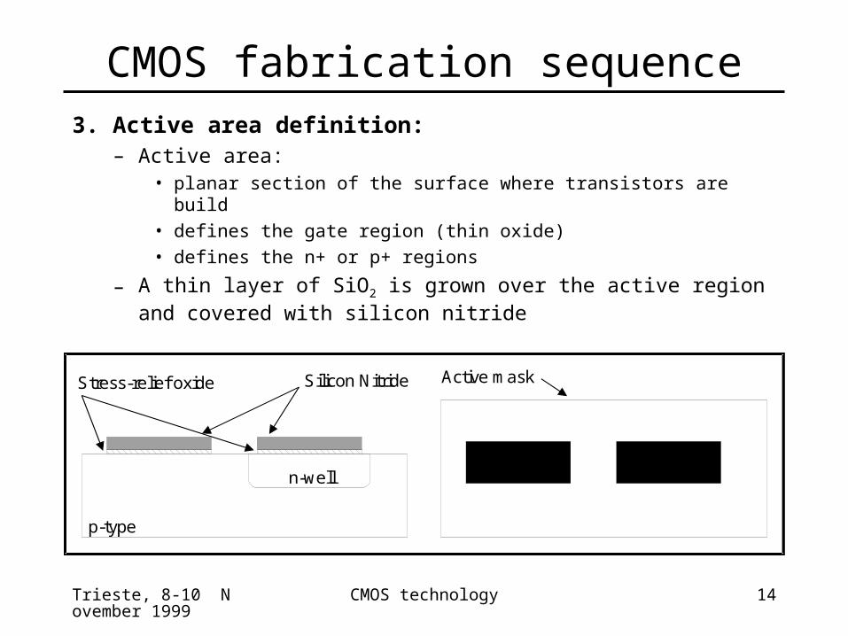
CMOS fabrication sequence3. Active area definition:
– Active area:• planar section of the surface where transistors are build• defines the gate region (thin oxide)• defines the n+ or p+ regions
– A thin layer of SiO2 is grown over the active region and covered with silicon nitride
n-well
Silicon NitrideStress-relief oxide
p-type
Active mask
Trieste, 8-10 November 1999
CMOS technology 15
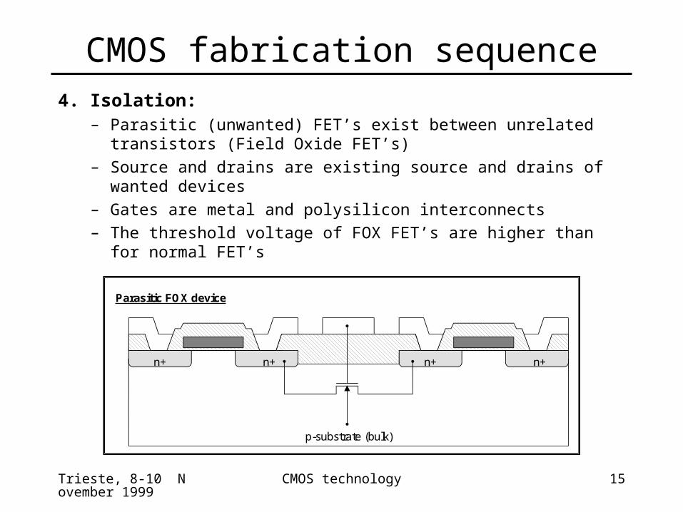
CMOS fabrication sequence4. Isolation:
– Parasitic (unwanted) FET’s exist between unrelated transistors (Field Oxide FET’s)
– Source and drains are existing source and drains of wanted devices
– Gates are metal and polysilicon interconnects
– The threshold voltage of FOX FET’s are higher than for normal FET’s
p-substrate (bulk)
n+ n+
Parasitic FOX device
n+ n+
Trieste, 8-10 November 1999
CMOS technology 16
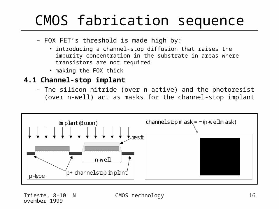
CMOS fabrication sequence– FOX FET’s threshold is made high by:
• introducing a channel-stop diffusion that raises the impurity concentration in the substrate in areas where transistors are not required
• making the FOX thick
4.1 Channel-stop implant– The silicon nitride (over n-active) and the photoresist (over n-well)
act as masks for the channel-stop implant
n-well
p-type
channel stop mask = ~(n-well mask)
resit
Implant (Boron)
p+ channel-stop implant
Trieste, 8-10 November 1999
CMOS technology 17
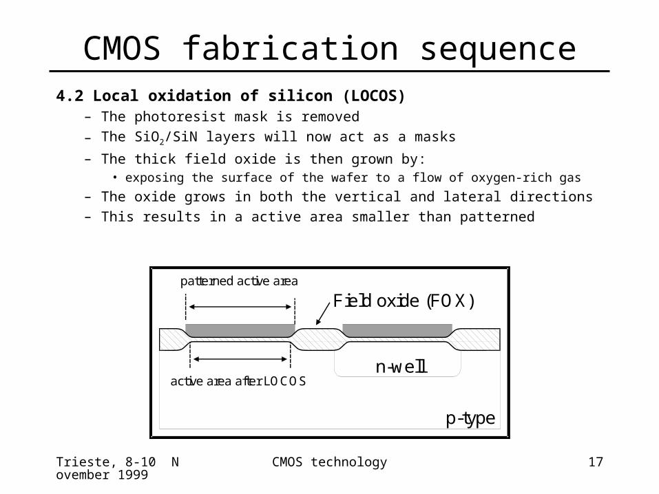
CMOS fabrication sequence4.2 Local oxidation of silicon (LOCOS)
– The photoresist mask is removed
– The SiO2/SiN layers will now act as a masks
– The thick field oxide is then grown by:• exposing the surface of the wafer to a flow of oxygen-rich gas
– The oxide grows in both the vertical and lateral directions– This results in a active area smaller than patterned
n-well
p-type
Field oxide (FOX)patterned active area
active area after LOCOS
Trieste, 8-10 November 1999
CMOS technology 18
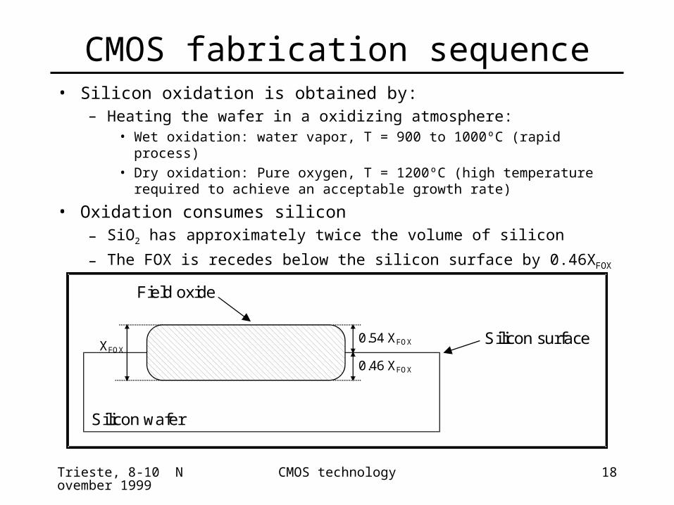
CMOS fabrication sequence• Silicon oxidation is obtained by:
– Heating the wafer in a oxidizing atmosphere:• Wet oxidation: water vapor, T = 900 to 1000ºC (rapid process)• Dry oxidation: Pure oxygen, T = 1200ºC (high temperature required to
achieve an acceptable growth rate)
• Oxidation consumes silicon– SiO2 has approximately twice the volume of silicon
– The FOX is recedes below the silicon surface by 0.46XFOX
XFOX
0.54 XFOX
0.46 XFOX
Silicon wafer
Silicon surface
Field oxide
Trieste, 8-10 November 1999
CMOS technology 19
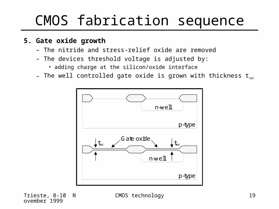
CMOS fabrication sequence5. Gate oxide growth
– The nitride and stress-relief oxide are removed
– The devices threshold voltage is adjusted by:• adding charge at the silicon/oxide interface
– The well controlled gate oxide is grown with thickness tox
n-well
p-type
n-well
p-type
tox tox
Gate oxide
Trieste, 8-10 November 1999
CMOS technology 20
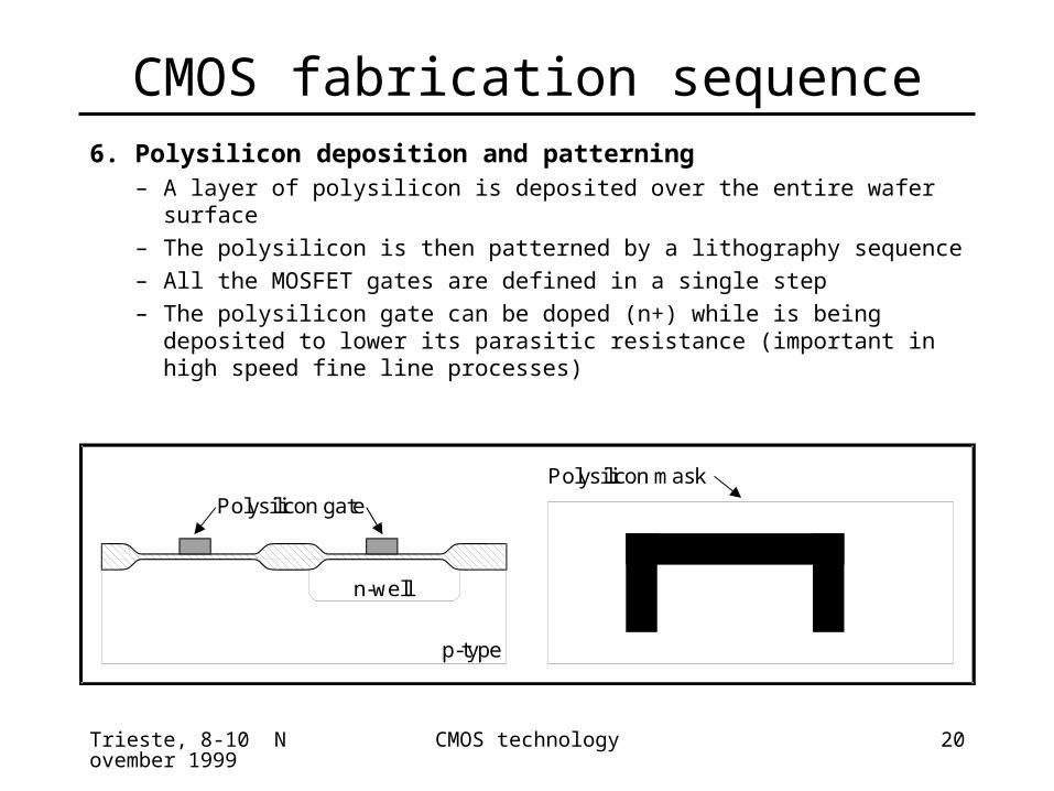
CMOS fabrication sequence6. Polysilicon deposition and patterning
– A layer of polysilicon is deposited over the entire wafer surface
– The polysilicon is then patterned by a lithography sequence
– All the MOSFET gates are defined in a single step
– The polysilicon gate can be doped (n+) while is being deposited to lower its parasitic resistance (important in high speed fine line processes)
n-well
p-type
Polysilicon gate
Polysilicon mask
Trieste, 8-10 November 1999
CMOS technology 21
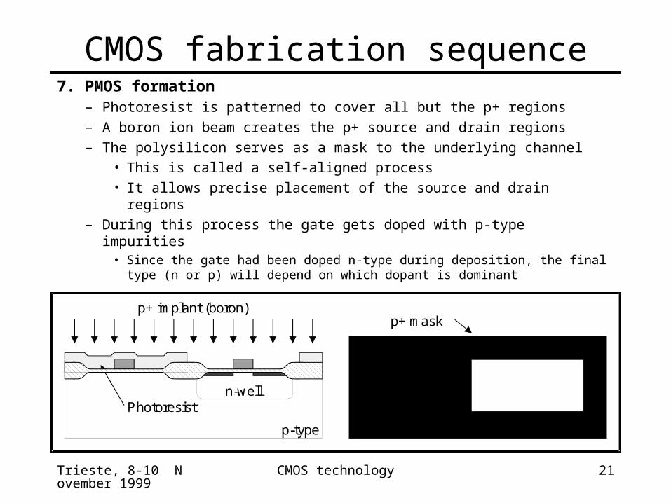
CMOS fabrication sequence7. PMOS formation
– Photoresist is patterned to cover all but the p+ regions
– A boron ion beam creates the p+ source and drain regions
– The polysilicon serves as a mask to the underlying channel
• This is called a self-aligned process
• It allows precise placement of the source and drain regions
– During this process the gate gets doped with p-type impurities• Since the gate had been doped n-type during deposition, the final type
(n or p) will depend on which dopant is dominant
n-well
p-type
p+ implant (boron)p+ mask
Photoresist
Trieste, 8-10 November 1999
CMOS technology 22
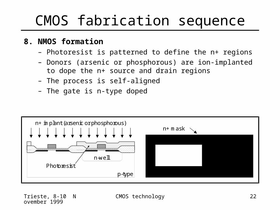
CMOS fabrication sequence8. NMOS formation
– Photoresist is patterned to define the n+ regions
– Donors (arsenic or phosphorous) are ion-implanted to dope the n+ source and drain regions
– The process is self-aligned
– The gate is n-type doped
n-well
p-type
n+ implant (arsenic or phosphorous)n+ mask
Photoresist
Trieste, 8-10 November 1999
CMOS technology 23
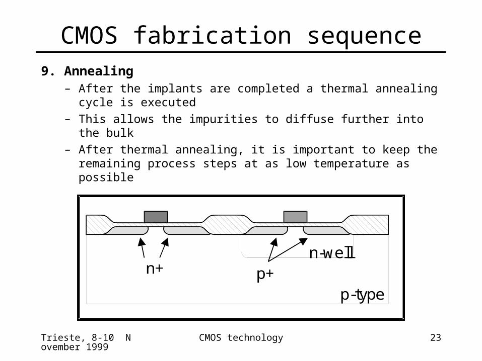
CMOS fabrication sequence9. Annealing
– After the implants are completed a thermal annealing cycle is executed
– This allows the impurities to diffuse further into the bulk
– After thermal annealing, it is important to keep the remaining process steps at as low temperature as possible
n-well
p-type
n+ p+
Trieste, 8-10 November 1999
CMOS technology 24
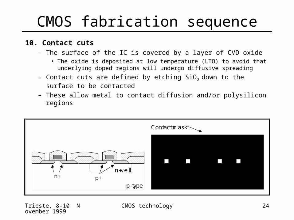
CMOS fabrication sequence10. Contact cuts
– The surface of the IC is covered by a layer of CVD oxide• The oxide is deposited at low temperature (LTO) to avoid that
underlying doped regions will undergo diffusive spreading
– Contact cuts are defined by etching SiO2 down to the surface to be contacted
– These allow metal to contact diffusion and/or polysilicon regions
n-well
p-type
n+ p+
Contact mask
Trieste, 8-10 November 1999
CMOS technology 25
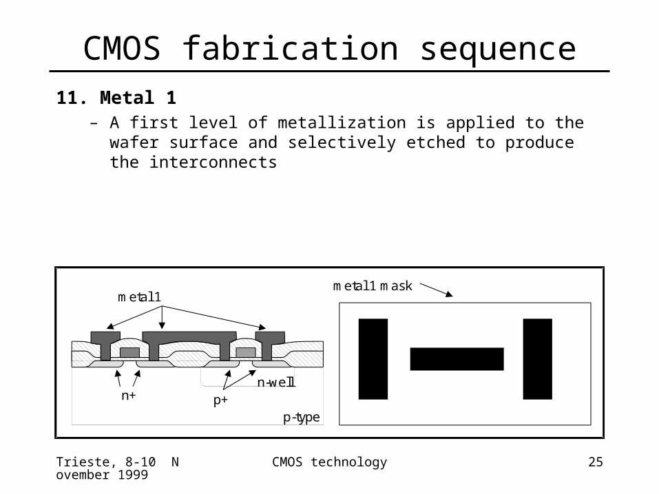
CMOS fabrication sequence11. Metal 1
– A first level of metallization is applied to the wafer surface and selectively etched to produce the interconnects
n-well
p-type
n+ p+
metal 1 maskmetal 1
Trieste, 8-10 November 1999
CMOS technology 26
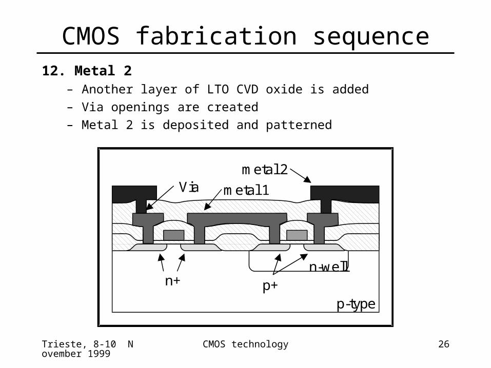
CMOS fabrication sequence12. Metal 2
– Another layer of LTO CVD oxide is added
– Via openings are created
– Metal 2 is deposited and patterned
n-well
p-type
n+ p+
Via metal 1
metal 2
Trieste, 8-10 November 1999
CMOS technology 27
CMOS fabrication sequence13. Over glass and pad openings
– A protective layer is added over the surface:
– The protective layer consists of:• A layer of SiO2
• Followed by a layer of silicon nitride
– The SiN layer acts as a diffusion barrier against contaminants (passivation)
– Finally, contact cuts are etched, over metal 2, on the passivation to allow for wire bonding.
Trieste, 8-10 November 1999
CMOS technology 28
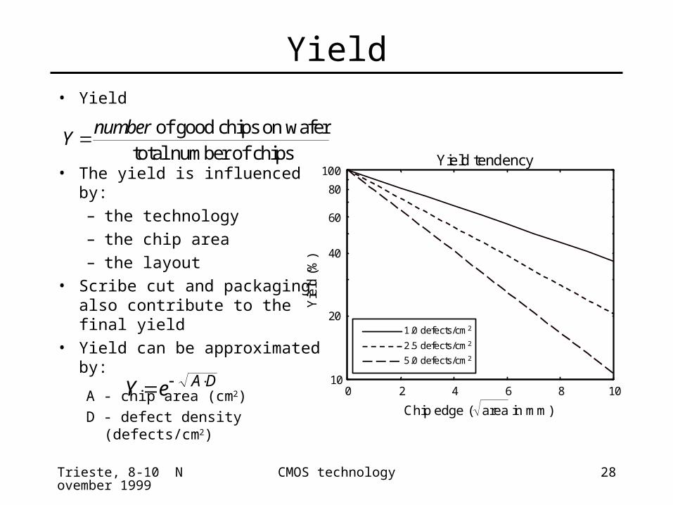
Yield• Yield
• The yield is influenced by:– the technology– the chip area– the layout
• Scribe cut and packaging also contribute to the final yield
• Yield can be approximated by:
A - chip area (cm2)
D - defect density (defects/cm2)
Ynumber of good chips on wafer
total number of chips
Y e A D 0 2 4 6 8 10
10
100
Yie
ld (
%)
Yield tendency
20
40
60
80
1.0 defects/cm2
2.5 defects/cm2
5.0 defects/cm2
Chip edge ( area in mm)
Trieste, 8-10 November 1999
CMOS technology 29
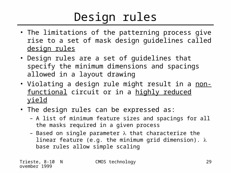
Design rules• The limitations of the patterning process give rise to a
set of mask design guidelines called design rules• Design rules are a set of guidelines that specify the
minimum dimensions and spacings allowed in a layout drawing
• Violating a design rule might result in a non-functional circuit or in a highly reduced yield
• The design rules can be expressed as:– A list of minimum feature sizes and spacings for all the
masks required in a given process– Based on single parameter that characterize the linear
feature (e.g. the minimum grid dimension). base rules allow simple scaling
Trieste, 8-10 November 1999
CMOS technology 30
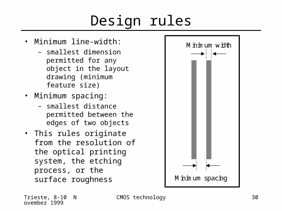
Design rules• Minimum line-width:
– smallest dimension permitted for any object in the layout drawing (minimum feature size)
• Minimum spacing:– smallest distance permitted
between the edges of two objects
• This rules originate from the resolution of the optical printing system, the etching process, or the surface roughness
Minimum spacing
Minimum width
Trieste, 8-10 November 1999
CMOS technology 31
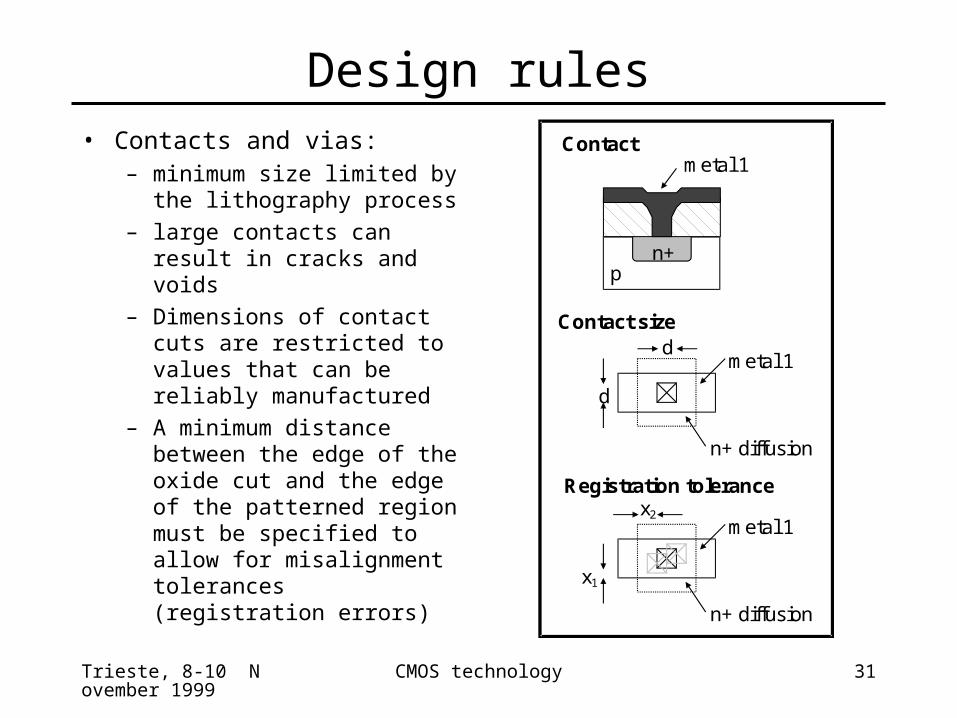
Design rules• Contacts and vias:
– minimum size limited by the lithography process
– large contacts can result in cracks and voids
– Dimensions of contact cuts are restricted to values that can be reliably manufactured
– A minimum distance between the edge of the oxide cut and the edge of the patterned region must be specified to allow for misalignment tolerances (registration errors)
n+p
metal 1
n+ diffusion
metal 1
d
dContact size
Registration tolerance
Contact
x2
n+ diffusion
metal 1
x1
Trieste, 8-10 November 1999
CMOS technology 32
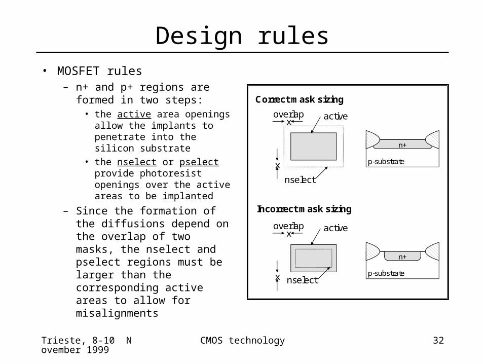
Design rules• MOSFET rules
– n+ and p+ regions are formed in two steps:
• the active area openings allow the implants to penetrate into the silicon substrate
• the nselect or pselect provide photoresist openings over the active areas to be implanted
– Since the formation of the diffusions depend on the overlap of two masks, the nselect and pselect regions must be larger than the corresponding active areas to allow for misalignments
Correct mask sizing
overlap
x
xactive
nselect
n+
p-substrate
Incorrect mask sizing
overlap
x
xactive
nselectp-substrate
n+
Trieste, 8-10 November 1999
CMOS technology 33
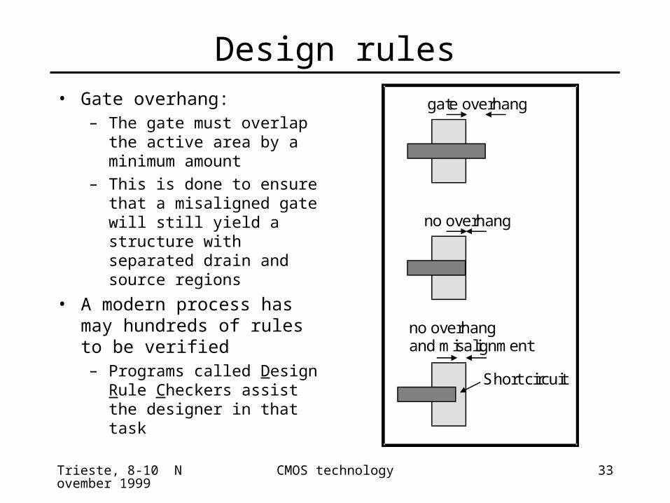
Design rules• Gate overhang:
– The gate must overlap the active area by a minimum amount
– This is done to ensure that a misaligned gate will still yield a structure with separated drain and source regions
• A modern process has may hundreds of rules to be verified– Programs called Design
Rule Checkers assist the designer in that task
gate overhang
no overhang
no overhangand misalignment
Short circuit
Trieste, 8-10 November 1999
CMOS technology 34
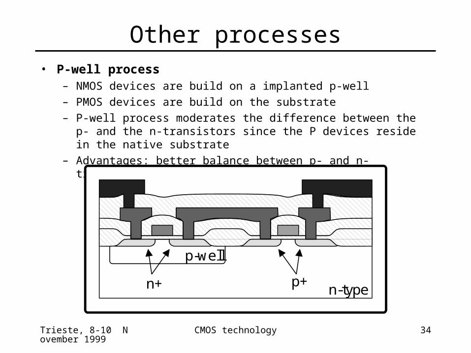
Other processes• P-well process
– NMOS devices are build on a implanted p-well
– PMOS devices are build on the substrate
– P-well process moderates the difference between the p- and the n-transistors since the P devices reside in the native substrate
– Advantages: better balance between p- and n-transistors
p-well
n-typen+ p+
Trieste, 8-10 November 1999
CMOS technology 35
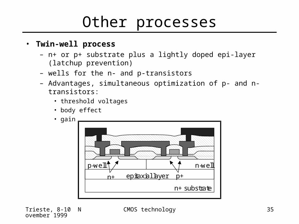
Other processes• Twin-well process
– n+ or p+ substrate plus a lightly doped epi-layer (latchup prevention)
– wells for the n- and p-transistors
– Advantages, simultaneous optimization of p- and n-transistors:• threshold voltages• body effect• gain
p-well
n+ substrate
n+ p+
n-well
epitaxial layer
Trieste, 8-10 November 1999
CMOS technology 36
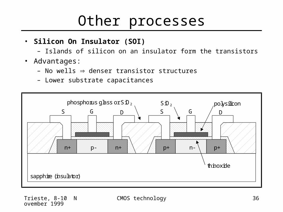
Other processes• Silicon On Insulator (SOI)
– Islands of silicon on an insulator form the transistors
• Advantages:– No wells denser transistor structures
– Lower substrate capacitances
n+ p- n+
S DG
p+ n- p+
S DG
sapphire (insulator)
polysilicon
thinoxide
SiO2phosphorus glass or SiO2
Trieste, 8-10 November 1999
CMOS technology 37
Other processes– Very low leakage currents– No FOX FET exists between unrelated devices– No latchup– No body-effect:
• However, the absence of a backside substrate can give origin to the “kink effect”
– Radiation tolerance
• Disadvantages:– Absence of substrate diodes (hard to implement protection
circuits)– Higher number of substrate defects lower gain devices– More expensive processing
Trieste, 8-10 November 1999
CMOS technology 38
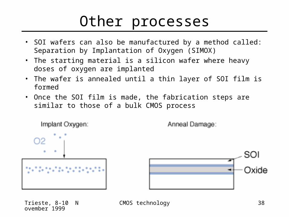
Other processes• SOI wafers can also be manufactured by a method called:
Separation by Implantation of Oxygen (SIMOX)• The starting material is a silicon wafer where heavy doses of
oxygen are implanted• The wafer is annealed until a thin layer of SOI film is formed• Once the SOI film is made, the fabrication steps are similar to
those of a bulk CMOS process
Trieste, 8-10 November 1999
CMOS technology 39
Advanced CMOS processes
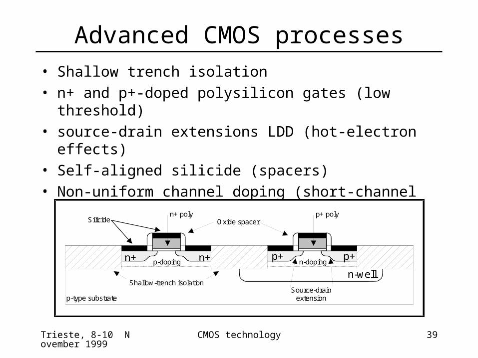
• Shallow trench isolation• n+ and p+-doped polysilicon gates (low threshold)• source-drain extensions LDD (hot-electron effects)• Self-aligned silicide (spacers)• Non-uniform channel doping (short-channel effects)
n-well
p+ p+n+ n+p-doping n-doping
Silicide Oxide spacern+ poly p+ poly
Shallow-trench isolation
p-type substrateSource-drain
extension
Trieste, 8-10 November 1999
CMOS technology 40
Process enhancements
• Up to six metal levels in modern processes• Copper for metal levels 2 and higher• Stacked contacts and vias• Chemical Metal Polishing for technologies with
several metal levels• For analogue applications some processes offer:
– capacitors– resistors– bipolar transistors (BiCMOS)
Trieste, 8-10 November 1999
CMOS technology 41
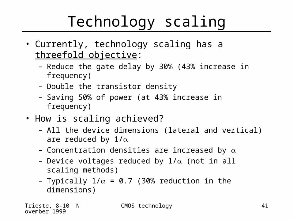
Technology scaling
• Currently, technology scaling has a threefold objective:– Reduce the gate delay by 30% (43% increase in frequency)– Double the transistor density– Saving 50% of power (at 43% increase in frequency)
• How is scaling achieved?– All the device dimensions (lateral and vertical) are reduced
by 1/ – Concentration densities are increased by – Device voltages reduced by 1/ (not in all scaling methods)– Typically 1/ = 0.7 (30% reduction in the dimensions)
Trieste, 8-10 November 1999
CMOS technology 42
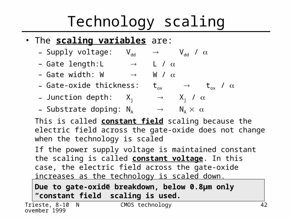
Technology scaling• The scaling variables are:
– Supply voltage: Vdd Vdd /
– Gate length: L L / – Gate width: W W / – Gate-oxide thickness: tox tox /
– Junction depth: Xj Xj /
– Substrate doping: NA NA
This is called constant field scaling because the electric field across the gate-oxide does not change when the technology is scaled
If the power supply voltage is maintained constant the scaling is called constant voltage. In this case, the electric field across the gate-oxide increases as the technology is scaled down.
Due to gate-oxide breakdown, below 0.8µm only “constant field” scaling is used.
Trieste, 8-10 November 1999
CMOS technology 43
Technology scaling
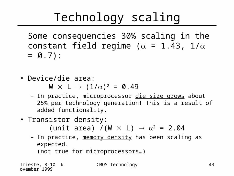
Some consequencies 30% scaling in the constant field regime ( = 1.43, 1/ = 0.7):
• Device/die area:W L (1/)2 = 0.49
– In practice, microprocessor die size grows about 25% per technology generation! This is a result of added functionality.
• Transistor density:(unit area) /(W L) 2 = 2.04
– In practice, memory density has been scaling as expected. (not true for microprocessors…)
Trieste, 8-10 November 1999
CMOS technology 44
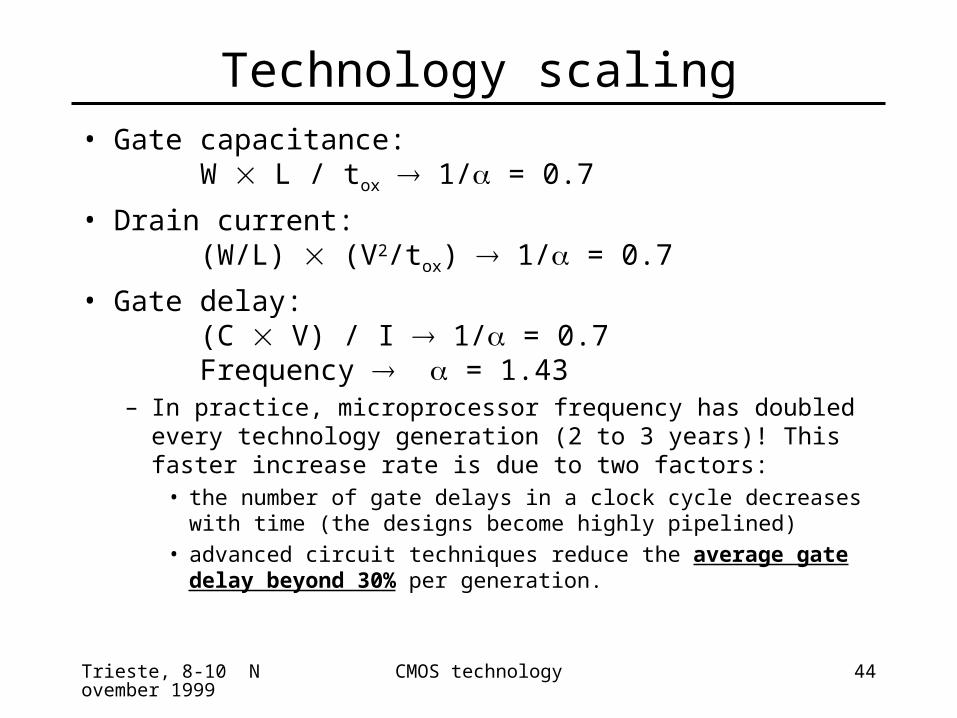
Technology scaling• Gate capacitance:
W L / tox 1/ = 0.7
• Drain current:(W/L) (V2/tox) 1/ = 0.7
• Gate delay:(C V) / I 1/ = 0.7Frequency = 1.43
– In practice, microprocessor frequency has doubled every technology generation (2 to 3 years)! This faster increase rate is due to two factors:
• the number of gate delays in a clock cycle decreases with time (the designs become highly pipelined)
• advanced circuit techniques reduce the average gate delay beyond 30% per generation.
Trieste, 8-10 November 1999
CMOS technology 45
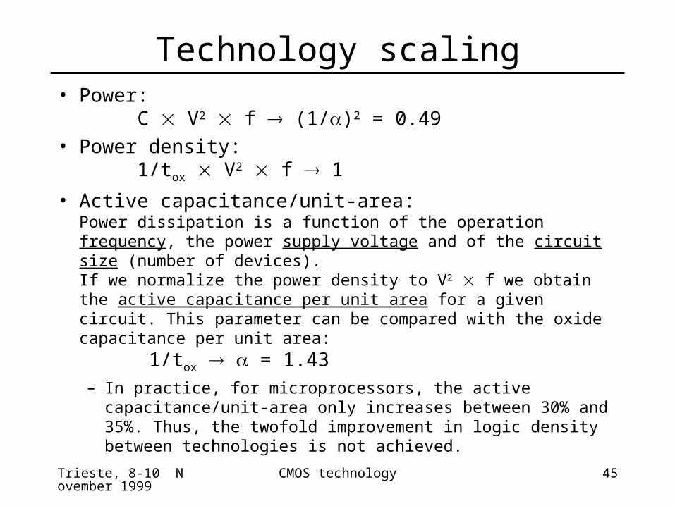
Technology scaling• Power:
C V2 f (1/)2 = 0.49• Power density:
1/tox V2 f 1
• Active capacitance/unit-area:Power dissipation is a function of the operation frequency, the power supply voltage and of the circuit size (number of devices).If we normalize the power density to V2 f we obtain the active capacitance per unit area for a given circuit. This parameter can be compared with the oxide capacitance per unit area:
1/tox = 1.43– In practice, for microprocessors, the active capacitance/unit-
area only increases between 30% and 35%. Thus, the twofold improvement in logic density between technologies is not achieved.
Trieste, 8-10 November 1999
CMOS technology 46
Technology scaling
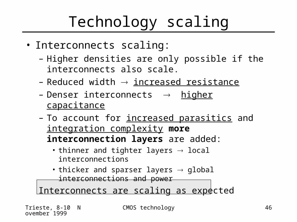
• Interconnects scaling:– Higher densities are only possible if the
interconnects also scale.– Reduced width increased resistance– Denser interconnects higher capacitance– To account for increased parasitics and integration
complexity more interconnection layers are added:
• thinner and tighter layers local interconnections• thicker and sparser layers global interconnections and
power
Interconnects are scaling as expected
Trieste, 8-10 November 1999
CMOS technology 47
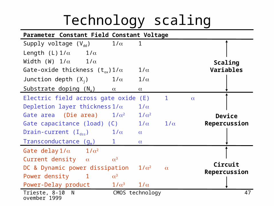
Technology scalingParameter Constant Field Constant Voltage
Supply voltage (Vdd) 1/ 1
Length (L) 1/ 1/Width (W) 1/ 1/Gate-oxide thickness (tox) 1/ 1/
Junction depth (Xj) 1/ 1/
Substrate doping (NA)
Electric field across gate oxide (E)1 Depletion layer thickness 1/ 1/Gate area (Die area) 1/2 1/2
Gate capacitance (load) (C) 1/ 1/Drain-current (Idss) 1/
Transconductance (gm) 1
Gate delay 1/ 1/2
Current density 3
DC & Dynamic power dissipation 1/2 Power density 1 3
Power-Delay product 1/3 1/
ScalingVariables
DeviceRepercussion
CircuitRepercussion
Trieste, 8-10 November 1999
CMOS technology 48
Technology scaling
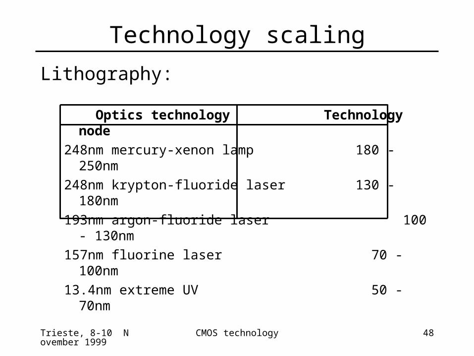
Lithography:
Optics technology Technology node
248nm mercury-xenon lamp 180 - 250nm
248nm krypton-fluoride laser 130 - 180nm
193nm argon-fluoride laser 100 - 130nm
157nm fluorine laser 70 - 100nm
13.4nm extreme UV 50 - 70nm
Trieste, 8-10 November 1999
CMOS technology 49
Technology scaling
Lithography:• Electron Beam Lithography (EBL)
– Patterns are derived directly from digital data– The process can be direct: no masks– Pattern changes can be implemented quickly– However:
• Equipment cost is high• Large amount of time required to access all the points on
the wafer
Top Related