


Languages
Pages
Legal


The effect of Germanium additions on SN100C
Nihon Superior Co., Ltd.

What is SN100C?
SN100C is a lead-free solder that is based onthe Tin-Copper Eutectic: Sn-0.7Cu
Germanium (Ge).
with a trace addition of Ni at a very specific leveland

Ⅰ- The effect of bridge elimination
The effect of Germanium additions

The effect of bridge elimination on SN100C
100pin 0.5mm pitch QFPWave soldering With SN100C
SN100C makes bridge-free soldering possibleeven with 100pin 0.5mm pitch QFP.

The mechanism of bridging
Whether or not bridging occurs depends on what happens as the joint exits the wave
(the “peel back” area)

The Peel-BackAreaSolder is draining off
the joint area back into the solder bath
If drainage is good there is no excess solder left on the joints
The mechanism of bridgingWhether or not bridging occurs depends on what
happens as the joint exits the wave(the “peel back” area)
So there is no solder to form a bridge

If drainage is not good there is excess solder left on the joints
The mechanism of bridgingWhether or not bridging occurs depends on what
happens as the joint exits the wave(the “peel back” area)
This excess solder forms a bridge

The mechanism of bridging
To study the effect of bridge elimination, the icicle test was carried out and the drainage characteristic of solder wave were confirmed.
Whether or not bridging occurs depends on what happens as the joint exits the wave (the “peel back” area)

The mechanism of bridging
[Results]1. The Ni addition to the Sn-Cu lead-free increases fluidity of the
solder and eliminates bridging.2. The addition of Ge to the Sn-Cu-Ni alloy to make “SN100C”
improves the drainage properties of the solder to further reduce any tendency to bridging.
Whether or not bridging occurs depends on what happens as the joint exits the wave (the “peel back” area)
To study the effect of bridge elimination, the icicle test was carried out and the drainage characteristic of solder wave were confirmed.

[Test conditions]・Test piece: Oxygen free copper ring (20mm ID, wire diameter 2.0mm)・Solder alloys: SC, SCN, SN100C, SCNP, SC0.3A, SCAB, S3A0.5C, S37P・Flux: JIS Standard flux A and B・Melting temperature: 255 ℃
(235℃ only for S37P)・Immersion depth: 6mm・Immersion speed: 4mm/s・Immersion time: 20s・Withdrawal speed: 2mm/s
つららの長さ
Test piece: Oxygen free copper ring
Before dipping
After dipping
IcicleIcicle length
Wetting balance test equipment(Tarutin Kester)
*High Speed CameraMEMRECAMfx K4(nac Image Technology., Inc. )
Icicle test

Oxygen Free Copper Ring
・Flux: JIS Standard Flux A, B・Melting Temp.: 255℃・Immersion Depth: 6mm・Immersion Speed: 4mm/s・Immersion Time: 20s・Withdrawal time: 2mm/s
20mm
2.0 mm Ø
Solder Bath
Icicle test

Icicle test
S37P
S3A0.5C
SCAB
SC0.3A
SCNP
SN100C
SCN
SC
37RSP system
3.00.5RSAC system
0.3
0.3
Ag
0.010.050.7R
0.10.7R
0.7RSCA system
0.050.050.5R
0.050.7R
SCN system
0.7R SC system
GeBiPNiCuPbSn
Solder alloy samples (%)

Test results1315
12061144
998
819
386285
174
0
200
400
600
800
1000
1200
1400
S37P
(235
℃)
S3A0
.5C
SC0.3
A
SCAB SC
SCNP SC
N
SN10
0C
はんだ材料
つら
らの
長さ
(μ
m)
The effect of Ni
The effect of Ge
Sn-Cu-Ni
Flux: JIS Standard flux A
Icic
le le
ngth
(μm
)
Solder alloy

The effect of bridge elimination on SN100C
The effect of Ni “plus Ge”
SN100C makes bridge-free soldering possibleeven with 100pin 0.5mm pitch QFP.
100pin 0.5mm pitch QFPWave solderingwith SN100C

Ⅱ- Wetting properties
The effect of Germanium additions
2/3Fmax
T0 T2 T3 T4 T6T7 T8T1
Immersion period
Fmax
Heating time
Wet
ting
forc
e
Fend
Start of test Immersion
complete
Start of wetting
Zero-crossing time
Interval to 2/3Fmax
Maximum force resistered
Withdrawal commences
Withdrawal completedStages of through
hole soldering
Wetting rate
Incubation period
Maximum wetting force
Wetting rate after zero-
crossing time
Interval to 2/3Fmax
Component termination
Zero-crossing time
Total wetting time
Board Board
Cu land
Wetting test – Meniscographic method
Interval to zero wetting force

F
t
Wetting test – Meniscographic method
Immersion Period
Incubation Period

F
Fmax
2/3Fmax
t
Immersion Period
Incubation Period
Zero CrossingFirst Stage
Wetting
Second Stage
Wetting
Wetting method – Meniscographic method
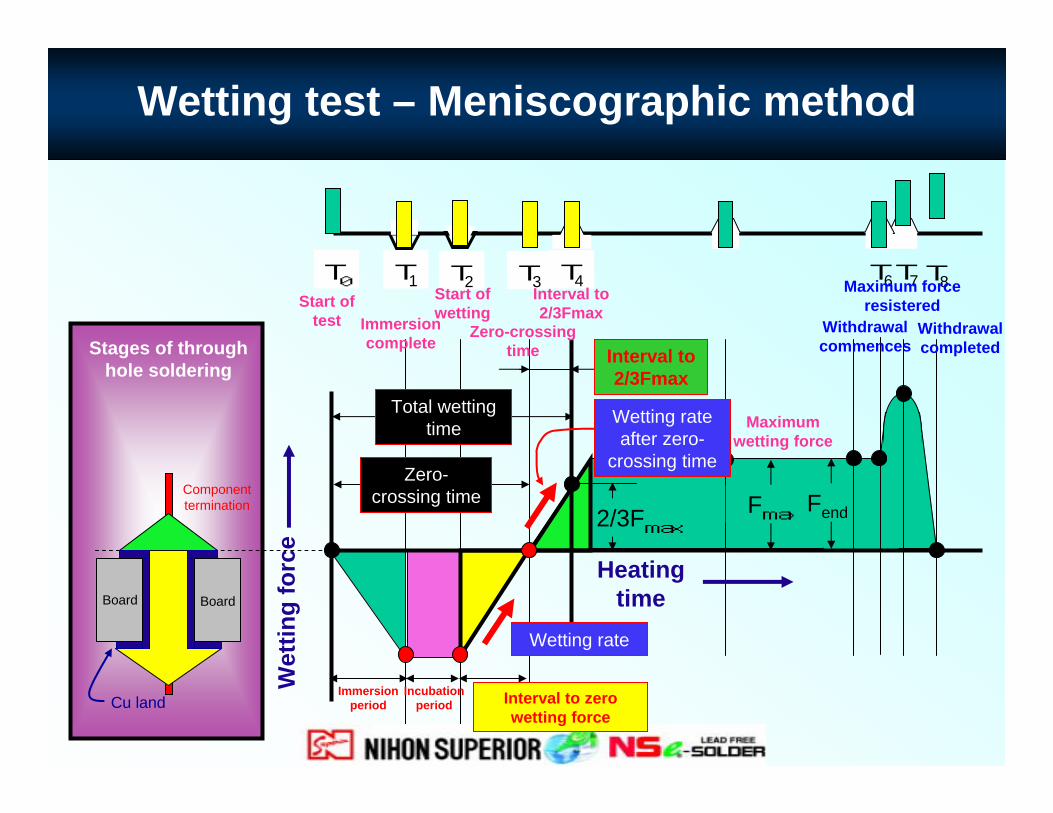
Test conditions[Test conditions]
・Test piece: Copper wire(wire diameter 0.6mm, length 30mm)
・Solder alloys: SN100C, SC, SCN, SCNP, SC0.3A, SCAB・Flux: JIS Standard flux B (for meniscographic test)・Melting temperature: 255℃
・Immersion time: 10 sec.・Immersion depth: 2 mm・Immersion speed: 2mm/s・Withdrawal speed: 2 mm/s
Test piece: Copper wire

-1.0
-0.5
0.0
0.5
1.0
0 0.5 1 1.5 2
時間(秒)
ぬれ
力(m
N)
SN100C SC SCN SCNP SC0.3A SCAB
SCNP takes longer to start wetting.
SCNP and SCA system take longer to start wetting after zero-crossing time.
Wetting properties of Sn-Cu system lead-free solderW
ettin
g fo
rce
(mN
)
Time (s)

2/3Fmax
T0 T2 T3 T4 T6T7 T8T1
Fmax
Heating time
Fend
Start of wetting
Start of wetting
Immersion complete
Start of wetting
Zero-crossing time
Interval to 2/3Fmax
Maximum force resistered
Withdrawal commences
Withdrawal completed
Maximum wetting force
Interval to 2/3F max
Zero-crossing
time
Total wetting time
Board Board
Cu landStart of wetting
Stages of through hole soldering
Component termination
Wet
ting
forc
e
Immersion period
Incubation period

Start of wetting
0.4 0.4 0.4
0.5
0.4 0.4
0.0
0.1
0.2
0.3
0.4
0.5
0.6
SN100C SCN SC SCNP SC0.3A SCAB
ぬれ
開始
時間
(se
c)
The disadvantage of P
Sta
rt of
wet
ting
(s)

2/3Fmax
T0 T2 T3 T4 T6T7 T8T1
Immersion time
FmaxFend
Interval to zero-wetting force
Incubation time
Zero-crossing time
Total wetting time
Board Board
Cu land Interval to zero wetting force
Stages of through hole soldering
Component termination
Start of wetting
Start of wetting
Interval to 2/3Fmax
Immersion complete
Zero-crossing time
Maximum force resistered
Withdrawal commences
Withdrawal completed
Maximum wetting force
Heating time
Wet
ting
forc
e

Interval to zero-wetting force
0.333 0.327
0.380
0.317
0.405
0.514
0.0
0.1
0.2
0.3
0.4
0.5
0.6
SN100C SCN SC SCNP SC0.3A SCAB
ぬれ
時間
(se
c)
The disadvantage of Bi
The effect of Ni
Inte
rval
to z
ero-
wet
ting
forc
e (s
)

2/3Fmax
T0 T2 T3 T4 T6T7 T8T1
FmaxFend
Interval to 2/3Fmax
Wetting rate
Interval to 2/3Fmax
Zero-crossing time
Total wetting time
Board Board
Cu land Interval to zero-wetting force
Start of wetting
Start of wetting
Interval to 2/3Fmax
Immersion complete
Zero-crossing time
Maximum force resistered
Withdrawal commences
Withdrawal completed
Maximum wetting force
Stages of through hole soldering
Heating time
Wet
ting
forc
e
Component termination
Immersion time
Incubation time

Interval to 2/3Fmax
0.1160.130 0.125
0.183
0.348
0.290
0.0
0.1
0.2
0.3
0.4
SN100C SCN SC SCNP SC0.3A SCAB
ぬれ
上が
り時
間(
sec
)
The effect of Ge
The disadvantage of P
The disadvantage of AgIn
terv
al to
2/3
Fmax
(s)

Total wetting time
0.849 0.860 0.9051.000
1.1531.203
0.0
0.2
0.4
0.6
0.8
1.0
1.2
1.4
SN100C SCN SC SCNP SC0.3A SCAB
総ぬ
れ時
間(
sec
)To
tal w
ettin
g tim
e (s
)
The effect of Ni and Ge

Ⅲ- The reduction of dross generation
The effect of Germanium additions

Method of measuring dross rates1. Desk-top mini-wave solder pot
・Solder capacity: 7kg・Bath dimensions: 130mm x 150mm・Nozzle dimensions: 30mm x 30mm・Fall distance from the jet outlet to the surface of the bath: 35-40mm
2. Melting temperature: 255℃
3. Precondition the bath by operating for 30minutes in airat constant pump speed.Remove the dross generated this preconditioning.Start the test with the preconditioned solder bath.
4. Collect the dross every hour for 4hours and weigh.Calculate the quantity of dross per hour for each alloy.

The images of dross
Sn-3.0Ag-0.5Cu Sn-0.7Cu Sn-0.7Cu-0.05NiSN100C
Sn-0.7Cu-0.05Ni+Ge
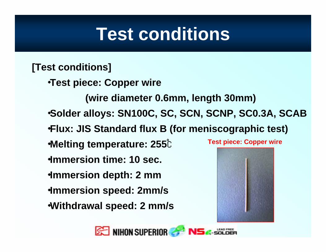
Dross generation
77.5
65.559.8 61.0
36.8
100%
84.5%
77.1% 78.7%
47.4%
0
20
40
60
80
100
120
Sn-3.0Ag-0.5Cu Sn-0.7Cu Sn-0.7Cu-0.3Ag Sn-0.7Cu-0.05N i SN100C
は ん だ 材 料
ドロ
ス発
生量
(g/
時間
)
0%
20%
40%
60%
80%
100%
120%
比率
(%
)
1時 間 当 たりの ドロ ス 発 生 量 (g/時 間 ) 比 率 (% )
The effect of Ge
The dross generation of SN100C is half as much as that of SAC305.
Dro
ss g
ener
atio
n (g
/hr)
Rat
io (%
)

Summary of the effect of Germanium additions

The effect of Germanium additions
ⅠBridge elimination
The beneficial effect of Ge on drainage combined with the beneficial
Ⅱ Faster wetting
The Ni addition accelerates initial wetting and the Ge addition
Ⅲ Reduced dross generation
The thin film that Ge forms on the surface of solder bath reduces the
effect of Ni on fluidity ensures minimum bridges.
accelerates wetting after zero-crossing.
formation of the tin oxide that is the basis of dross.
Top Related