
![Split-Ring Resonator Arrays for Electromagnetic Energy ...jpier.org/PIERB/pierb62/11.15012506.pdf · In an earlier work [17], we introduced metamaterial for electromangetic energy](https://static.fdocuments.net/doc/165x107/6042714138b0bc1a685c8317/split-ring-resonator-arrays-for-electromagnetic-energy-jpierorgpierbpierb6211.jpg)
![DESIGN AND ANALYSIS OF SPLIT RING RESONATOR BASED ...ictactjournals.in/paper/IJME_Vol_4_Iss_4_Paper_4_687_692.pdf · patch antenna [17], Polygon patch antenna [18], W-shaped microstrip](https://static.fdocuments.net/doc/165x107/5ffd0bf10bbfba4951293444/design-and-analysis-of-split-ring-resonator-based-patch-antenna-17-polygon.jpg)


![Improved Split-Ring Resonator for Microfluidicorca.cf.ac.uk/59763/1/Improved split ring.pdf · 2020. 11. 26. · The resonant frequency of a cavity resonator [13] is set by its dimensions,](https://static.fdocuments.net/doc/165x107/60f99d8762b1d658425e30d9/improved-split-ring-resonator-for-split-ringpdf-2020-11-26-the-resonant.jpg)


Languages
Pages
Legal

8/12/2019 Split Ring Resonator
http://slidepdf.com/reader/full/split-ring-resonator 1/6
8/12/2019 Split Ring Resonator
http://slidepdf.com/reader/full/split-ring-resonator 2/6
Mikrotalasna revija Decembar 2011.
8
particular structure we also need characteristic impedance Z eff ,
from which we determine effective equivalent parameters εeff and µeff . Complex propagation coefficient we obtain thefollowing way:
1 1 2 , (6)
where the sign is chosen based on condition
′′
0, which
tells us that a structure is passive. Formula for calculatingcharacteristic impedance is:
1 Г 1 Г · , (7)
where and are the characteristic impedances of
microstrip line and the air-filled microstrip line, and Г isreflection coefficient on transition from line to structure:
Г , (8)
where is characteristic impedance of the analyzed
equivalent microstrip structure.At last, final formula we need to calculate εeff and µeff is
their direct dependence from index of refraction: , (9)
and from equations (7) and (9) follows that: · ; . (10)
The assumption used above is that structure is symmetric,which is not always the case. For non-symmetric structure,averaging of S parameters is used: . (11)
III. STRUCTURE ANALYSIS
We proposed the basic configurationof multiband delay linewhich is realized on two-layer substrate (Fig. 1.).It consists of broadside coupled SRRs twisted by 90 degrees and a singleSRR, both coupled to microstrip line at the opposite sides.Thevertical via is placed in the middle between split-ring
resonators and short-circuited microstrip lint to ground. Allrelevant dimensions of the structure are given in Fig. 2.
Fig. 1.Layout of multiband delay line (basic configuration). The
upper substrate (dark gray) has r1=10.2 and thickness h1=0.635mm
and lower substrate (light gray) has r2=2.2 and thickness
h2=1.574mm
Broadside coupled SRRs twisted by 90 degrees are chosen
as a building block for delay line, since our previousinvestigation [5] discovered that such arrangement of SRRsexhibited the greatest group index of refraction and groupdelay. In this application we use only one pair of broadsidecoupled resonators instead of two pairs [5], that gives anarrower left-handed band as well as the range with enhanced
group delay.
Fig. 2. Relevant dimensions of the basic delay line in mm
In order to show how the main building parts of a delay line
influenceits overall characteristics: the single SRR and broadside coupled SRRs are simulated and compared in Figs.
3.-4.The real part of index of refraction and S 21 are given inFig. 3.while the group delay and imaginary part of index ofrefraction are shown in Fig. 4. It can be seen that bothresonators exhibitthe negative refractive index, but in differentfrequency bands and also three very pronounced peaks incharacteristic of group delay (additional peak is due to RH
band). Combining these two resonators in a proposed delayline (Fig. 1) their responses are simply added giving two left-handed and one right-handed bands.Comparison betweentwobroadside coupled resonatorstwisted by 90 degrees [4], [5]and the proposed delay line is shown in Fig. 5. It can be seenthat broadside coupled resonators have only one LH band,while delay line shows two LH bands, the first of which
comes from a single broadside coupled SRRs, while the otherone is due to resonance of a single SRR.
4.0 4.5 5.0 5.5 6.0 6.5 7.0 7.5 8.0
-15
-10
-5
0
5
R e a l p a r t o f r e f r a c t i v e i n d
e x , n '
f[GHz]
Single SRR
Single Broadside SRRs
-30
-20
-10
0
10
20
30
40
| S 2 1
| [ d B ]
Fig. 3. Real part of index of refraction simulated for the individual building blocks of multiband delay line (Fig. 1.)LH bands are
marked with rectangular bars
reference
plane
8/12/2019 Split Ring Resonator
http://slidepdf.com/reader/full/split-ring-resonator 3/6
December, 2011 Microwave Review
9
Position of the second LH band can be moved up and downchanging the dimensions and orientation of a single SRRas itis shown in Fig. 7. In that delay line we have used anelongated single SRR rotated by 180 degrees whose length is
30 or 50 percent longer than in a basic delay line.
4.0 4.5 5.0 5.5 6.0 6.5 7.0 7.5 8.0
-1000
0
1000
2000
3000
4000
5000
6000
G r o u p
d e
l a y ,
g
[ p s
]
f[GHz]
Single SRR
Single Broadside SRRs
3.4ns
2ns
-28
-24
-20
-16
-12
-8
-4
0
4
8
12
I m a g
i n a r y p a r t o
f i n d e x o
f r e
f r a c t i o n ,
n ' '
Fig. 4.Group delay and imaginary part of index of refraction
simulated for the individual building blocks of multiband delay line
4.0 4.5 5.0 5.5 6.0 6.5 7.0 7.5 8.0
-16
-12
-8
-4
0
4
R e a
l p a r t o
f i n d e x o
f r e
f r a c
t i o n ,
n '
f[GHz]
Single SRR
Broadside
coupled SRRs
-32
-24
-16
-8
0
8
16
24
32
| S 2 1
| [ d B ]
Double broadside coupled SRRs
Delay line
SRR by 900
Fig. 5.Real part of index of refraction and S 21 for broadsidecoupled SRRs placed symmetrically in respect to microstrip line
(double broadside) and a proposed delay line. The origin of eachresonance is indicated in diagram
4.0 4.5 5.0 5.5 6.0 6.5 7.0 7.5 8.0
-1000
0
1000
2000
3000
4000
5000
G r o u p
d e l a
y ,
g [ p s
]
f[GHz]
Double broadside coupled SRRs
Delay line
2.7ns
2.4ns
-28
-24
-20
-16
-12
-8
-4
0
4
8
12
I m a g
i n a r y p a r t o
f i n d e x o
f r e
f r a c
t i o n ,
n ' '
Fig. 6.Group delay and imaginary part of index of refraction(losses) for broadside coupled SRRs placed symmetrically in respect
to microstrip line (double broadside) and a proposed delay line
Fig. 7. Layout of the delay line with elongated single SRR. Itslength is 50 percent longer than the broadside coupled SRRs.
Multiband response S 21, index of refraction and group delayof an elongated delay line(Fig. 7.)are shown in Fig. 8. andcompared with the responsesof delay line whose single SRR
has a length 30 percent longer than broadside coupled SRRs.Rectangular bars denote the frequency ranges with negative
index of refraction. The first and the third bands areunchanged if the length of a single SRR is changed, since theyare caused by broadside coupled SRRs that are the same for
both cases. It is shown that the second band can be shifted tolower and upper frequencies depending of the length of the
single SRR.
4.0 4.5 5.0 5.5 6.0 6.5 7.0 7.5 8.0
-18
-16
-14
-12
-10
-8
-6
-4
-2
0
2
4
6
8
I n d e x o f r e f r a c t i o n , n
f[GHz]
n'
n''
-20
-15
-10
-5
0
5
10
15
20
25
Elongated SRR, L=1.3*Lo
Elongated SRR, L=1.5*Lo
| S 2 1
| [ d B ]
(a)
4.0 4.5 5.0 5.5 6.0 6.5 7.0 7.5 8.0
-1000
0
1000
2000
3000
4000
G r o u p
d e
l a y ,
g [ p s
]
f[GHz]
Elongated SRR, L=1.3*Lo
Elongated SRR, L=1.5*Lo
-25
-20
-15
-10
-5
0
5
10
I m a g
i n a r y p a r t o
f i n d e x o
f r e
f r a c
t i o n ,
n ' '
(b)
Fig. 8. Simulated results for the two lengths of elongatedsingle
SRR: (a) S 21 and index of refraction, n and (b) group delay, g andimaginary part of refractive index (losses)
8/12/2019 Split Ring Resonator
http://slidepdf.com/reader/full/split-ring-resonator 4/6
Mikrotalasna revija Decembar 2011.
10
IV. R ECONFIGURABILITY
It should be noted that rotation of SRRs presents nothingmore than changing the gap position, so it is possible torealize it electronically using PIN diodes, which would open
or close certain gaps. This approach would permit creation ofelectronically reconfigurable metamaterials, which
electromagnetic properties could be changed in real-time andadjusted to momentary needs.
To demonstrate reconfigurability of proposed multibanddelay line we simulated two simple modificationsof the basicdelay line: (a) with the single SRR closed and (b) with theupper broadside coupled SRR closed. Electronic
reconfigurability of the structure can be accomplished usingPIN diodes placed at the gap of the upper SRRs. Switchingthe biasof the diode ON or OFF it is possible to change theoperating regime of the delay line. Fig. 9 shows the layout oftwo modified delay lines.
(a) thesingle SRR closed (b) the upper broadside SRRclosed
Fig. 9.Layout of two simple modifications of the proposed delay line
Instead of closing SRR, the same electromagnetic response
can be obtained with double-cut SRR, for instance by placingthe additional gap at the opposite side ofthe existing one. Inthat case, PIN diode should be switched ON during the regular
operation, while in the case of the closedSRR,the diode should be in the ON state only when changing the basic mode ofoperation, that seems more convenient.
4.0 4.5 5.0 5.5 6.0 6.5 7.0 7.5 8.0
-24
-20
-16
-12
-8
-4
0
4
R e a l p a r t o f r e
f r a c t i v e i n d e x , n '
f[GHz]
-32
-24
-16
-8
0
8
16
24
Closed the upper broadside SRR
Basic delay line
| S 2 1
| [ d B ]
Fig. 10.Real part of index of refraction and S 21 for the upper
broadside SRR closed (Fig. 9b). Rectangular bars denote the changesin responses
Delay line with the single SRR closed (Fig. 9a), exhibits the
same response as the single broadside coupled SRRs (Fig. 3.and Fig. 4.). It can be seen that the novel delay line has onlytwo narrow, enhanced peaks in the characteristic of groupdelay: at 4.9GHz (3.4ns) and 6.75GHz (2ns), instead of three peaks: at 4.96GHz (2.7ns), 6.34GHz (1.1ns) and 6.8GHz(1.5ns).
Delay line with the upper broadside coupled SRR closed(Fig. 9b.), exhibits considerably changed characteristics inrespect to the basic delay line, as can be seen in Figs. 10 and11. The first resonance is moved at the higher frequency from4.96GHz to 5.98GHz, since there is no the broadside coupledSRRs. Instead of two LH bands, there is only upper left-handed band at the same frequency, while the RH band is
shifted down below the LH band (Fig. 10).
4.0 4.5 5.0 5.5 6.0 6.5 7.0 7.5 8.0
-1000
-500
0
500
1000
1500
2000
2500
3000
3500
4000
4500
5000
5500
6000
G r o u p d e l a
y ,
g [ p s ]
f[GHz]
Closed the upper broadside SRR
Basic delay line
-20
-16
-12
-8
-4
0
4
8
12
I m a g i n a r y p a r t o f i
n d e x o f r e f r a c t i o n , n ' '
Fig. 11.Group delay and imaginary part of index of refraction
(losses) for the upper broadside SRR closed (Fig. 9b). Rectangular bars denote the changes in responses
V. EXPERIMENTAL RESULTS
In order to verify our simulations, the delay line whichconsists of threeSRRs coupled to microstrip line (Fig. 1.), is
fabricated and measured using Agilent PNA E8364A NetworkAnalyzer. Network Analyzer is calibrated with customdesigned TRL set shown in Fig. 12a, which provides themeasurements of S -parameters at certain reference planes andalso eliminates the influence of SMA connectors.
(a)(b)
Fig. 12. Measurement set-up: (a) TRL calibration set, (b) Delayline with SRRs (see Fig. 3. for the details)
Measured S -parameters are used as an input data for theretrieval procedure based on Nicolson-Ross-Weir [4]
approach.
8/12/2019 Split Ring Resonator
http://slidepdf.com/reader/full/split-ring-resonator 5/6
December, 2011 Microwave Review
11
Simulated and measured S 21-parameter and extractedeffective index of refraction are shown in Fig. 13. Rectangular bars denote two clearly separated frequency bands withnegative refractive index, which is the difference in respect to
delay line consisting of two broad-side coupled SRRs whichhasthe negative refractive index only in the first band.The firsttwo peaks in the diagram of group delay (Fig. 14) correspondto left-handed bands while the third one is due to right-handed band. Since the first peak is consequence of the single broad-side coupled SRR it is somewhat narrower than in the case oftwo broad-side coupled SRRs [3].
4.0 4.5 5.0 5.5 6.0 6.5 7.0 7.5 8.0
-8
-4
0
4
I n d e x
o f r e f r a c t i o n , n = n ' - j n ' '
f[GHz]
n'
n"
-16
-12
-8
-4
0
4
8
12
16
20
24
28
Simulated
Mesured
| S 2 1
| [ d B ]
Fig. 13. Simulated and measured S 21and extracted real (n’ ) andimaginary part (n’’ ) of the effective index of refraction
4.5 5.0 5.5 6.0 6.5 7.0 7.5
-1000
-500
0
500
1000
1500
2000
2500
3000
G r o u p
d e
l a y ,
g
[ p s ]
f[GHz]
-4000
-3500
-3000
-2500
-2000
-1500
-1000
-500
0
500
1000
1500
Simulated
Measured
I n a g
i n a r y p a r t o
f i n d e x o
f r e
f r a c
t i o n ,
2 0 0 * n ' '
Fig. 14. Simulated and measured group delay ,g and imaginary part (n’’ ) of the effective index of refraction
Measured results show very good agreement withsimulations concerning the shape and the amplitude of thecurves, but are shifted for about 6% in respect to simulationsdue to glue added between two substrates during fabrication
that is not taken into account in simulations.Maximum group delay is measured at the first band at
4.7GHz and is about 1.7ns, while next two peaks are at5.83GHz and 6.43GHz with delay of 0.94ns and 0.9nsrespectively. Those peaks correspond exactly to minimum inthe imaginary part of refractive index, n’’.
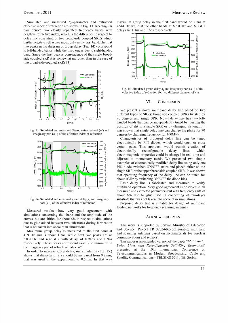
In order to increase group delay, our simulation (Fig. 15.)shows that diameter of via should be increased from 0.2mm,that was used in the experiment, to 0.5mm. In that way
maximum group delay in the first band would be 2.7ns at4.96GHz while at the other bands at 6.33GHz and 6.8GHzdelays are 1.1ns and 1.6ns respectively.
4.5 5.0 5.5 6.0 6.5 7.0 7.5
-1000
-500
0
500
1000
1500
2000
2500
3000
3500
4000
4500
G r o u p
d e
l a y , g
[ p s
]
f[GHz]
-4000
-3000
-2000
-1000
0
1000
2000
Via 0.2mm
Via 0.5mm
I m a g
i n a r y p a r t o
f i n d e x o f r e
f r a c
t i o n ,
2 0 0 * n ' '
Fig. 15. Simulated group delay ,g and imaginary part (n’’ ) of theeffective index of refraction for two different diameter of via
VI. CONCLUSION
We present a novel multiband delay line based on twodifferent types of SRRs: broadside coupled SRRs twisted by
90 degrees and single SRR. Novel delay line has two left-handed bands that can be independently tuned by twisting the
position of slit in a single SRR or by changing its length. Itwas shown that single delay line can change the phase for 70degrees by changing frequency for 100MHz.
Characteristics of proposed delay line can be tunedelectronically by PIN diodes, which would open or closecertain gaps. This approach would permit creation of
electronically reconfigurable delay lines, whichelectromagnetic properties could be changed in real-time and
adjusted to momentary needs. We presented two simpleexamples of electronically modified delay line using only onePIN diode switched ON/OFF states and placed either on thesingle SRR or the upper broadside coupled SRR. It was shownthat operating frequency of the delay line can be tuned forabout 1GHz by switching ON/OFF the diode bias.
Basic delay line is fabricated and measured to verify
multiband operation. Very good agreement is observed in allmeasured and extracted parameters but with frequency shift ofabout 6% due to glue used in connecting of two-layersubstrate that was not taken into account in simulations.
Proposed delay line is suitable for design of multiband
feeding networks for frequency scanning antennas.
ACKNOWLEDGEMENT
This work is supported by Serbian Ministry of Education
and Science (Project TR 32024-Reconfigurable, multibandand scanning antennas based on metamaterials for wirelesscommunications and sensors).
This paper is an extended version of the paper “ Multiband Delay Lines with Reconfigurable Split-Ring Resonators” presented at the 10th International Conference onTelecommunications in Modern Broadcasting, Cable and
Satellite Communications – TELSIKS 2011, Niš, Serbia.

8/12/2019 Split Ring Resonator
http://slidepdf.com/reader/full/split-ring-resonator 6/6
Mikrotalasna revija Decembar 2011.
12
R EFERENCES
[1] N. Liu, H. Liu, S. Zhu and H. Giessen,“Stereometamaterials”, Nature Photonics, vol.3, March2009, pp. 157-162.
[2] V. Milosevic, B. Jokanovic and B. Kolundzija,“Microwave sterometamaterials and parameter
extraction”, Metamaterials’2010, The Fifth InternationalCongress on Advanced Electromagnetic Materials inMicrowaves and Optics, Karlsruhe, Germany, 13.-18.September 2010.
[3] B. Jokanovic, V. Milosevic and R. Bojanic, “Theoreticaland experimental investigations of reconfigurable
metamaterials based on split-ring resonators”,
MediNano-3, 3rd Mediterranean Conference on Nanophotonics, Belgrade, Serbia, 18.-19. October 2010.
[4] S-G Mao, S-L Chen, C-W Huang, “EffectiveElectromagnetic Parameters of Novel Distributed Left-Handed Microstrip Lines”, IEEE Trans. Microw. TheoryTech., vol. 53, no. 4, pp. 1515-1521, Apr. 2005.
[5] W.B. Weir, “Automatic Measurement of ComplexDielectric Constant and Permeability at MicrowaveFrequencies”, Proceedings of the IEEE, vol. 62, no. 1,Jan. 1974.
Top Related