


Languages
Pages
Legal

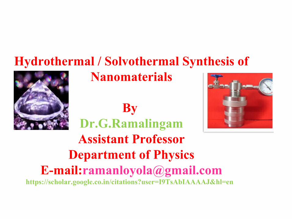
Hydrothermal / Solvothermal Synthesis ofNanomaterials
By Dr.G.RamalingamAssistant Professor
Department of PhysicsE-mail:[email protected]
https://scholar.google.co.in/citations?user=I9TsAbIAAAAJ&hl=en
Hydrothermal / Solvothermal Synthesis ofNanomaterials
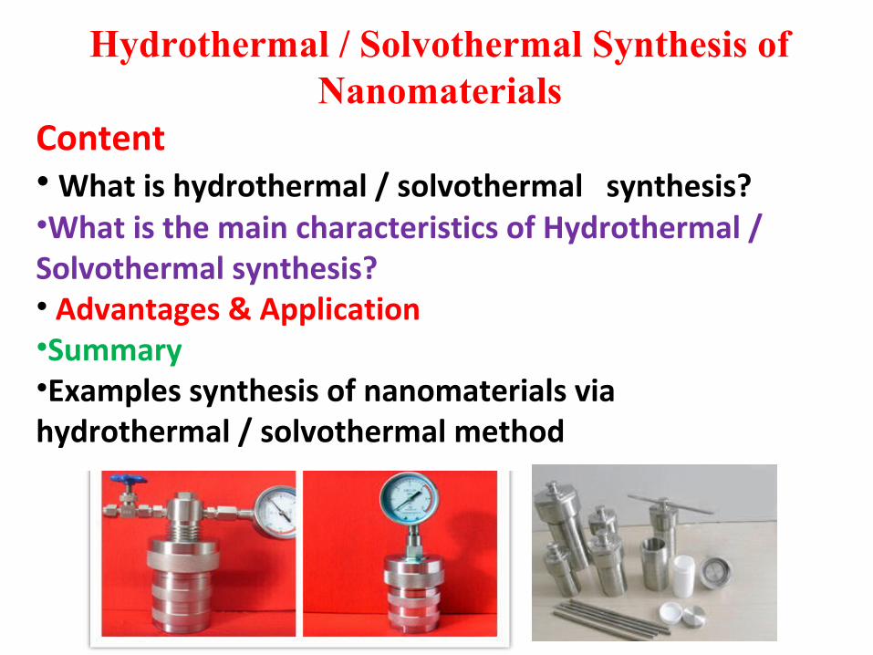
Content• What is hydrothermal / solvothermal synthesis?•What is the main characteristics of Hydrothermal / Solvothermal synthesis?• Advantages & Application •Summary •Examples synthesis of nanomaterials via hydrothermal / solvothermal method

BRIEF HISTORY OF THE SOLVOTHERMALCRYSTAL GROWTH OF LARGE SINGLE CRYSTALS
The history of the solvothermal Crystal Growth is closely related to The history of the solvothermal Crystal Growth is closely related to the hydrothermal crystal growth of the hydrothermal crystal growth of αα-quartz.-quartz.
due to:
→ its piezoelectric properties (leading to important applications)
→ its low temperature domain of stability (Tα-quartz → Tβ-quartz = 573°C) (impeding the use of conventional Crystal-growth processes)
→The elaboration of α-quartz single crystals was the first example for industrial developments of Hydrothermal Crystal Growth.
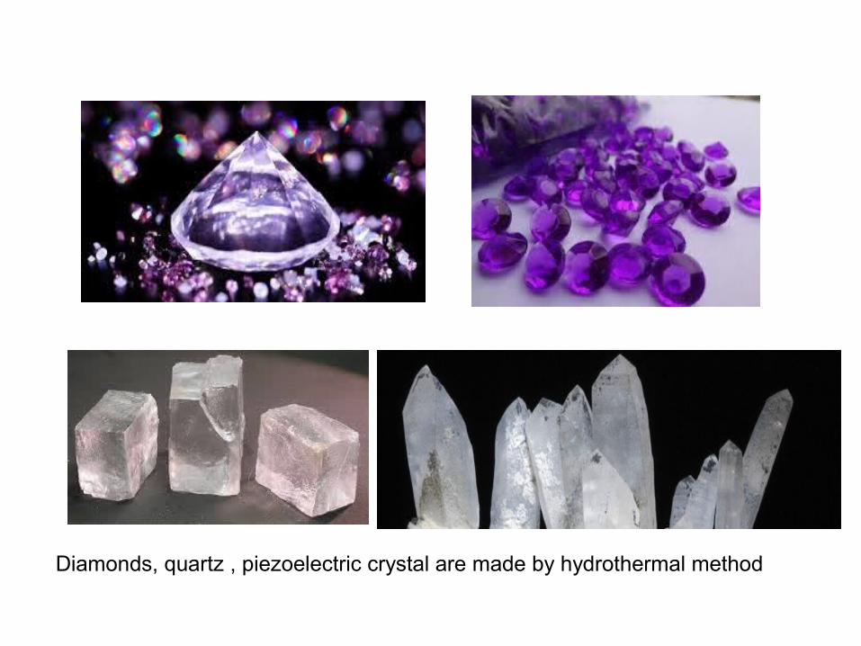
Diamonds, quartz , piezoelectric crystal are made by hydrothermal method
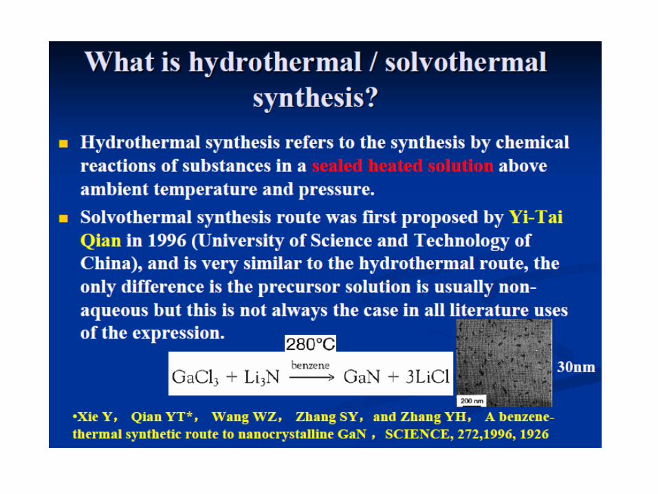
A “solvothermal reaction can be defined as a chemical reaction (or a transformation) between precursor(s) in a solvent (in a close system) at a temperature higher than the boiling temperature of this solvent and under high
pressure”
→ autogeneous pressure or imposed pressure.→ Subcritical or supercritical domain.→ Homogeneous or heterogeneous system.
SOLVOTHERMAL REACTIONS
SOLVOTHERMAL PROCESSES: FROM NOVEL MATERIALS TO HYBRID NANO-SYSTEMS.

7
SOLVOTHERMAL PROCESS
The term « SOLVOTHERMAL » was proposed at the beginning of the 90’s (G. DEMAZEAU et al.) during the development of non-aqueous solvents.
Examples.
⇒ Synthesis and crystal growth of nitrides using liquid ammonia (NH3) as solvent → ammothermal process !
⇒ Synthesis and crystal growth of Fe3O4 as small single crystals using C2H5OH as solvent → alcoholothermal process…!
Consequently each solvent can lead to a specific « word » for different processes characterized by the same features.
SOLVO – THERMAL
Solvent use of the temperature

New Trends in Solvothermal Crystal Growth Processes
MAIN FACTORS GOVERNING THE SOLVOTHERMAL CRYSTAL GROWTHMAIN FACTORS GOVERNING THE SOLVOTHERMAL CRYSTAL GROWTH
CHEMICAL FACTORSCHEMICAL FACTORS
PHYSICAL FACTORSPHYSICAL FACTORS
KINETICAL FACTORSKINETICAL FACTORS
- nature of the solvent,- nature of the nutrient,- nature of the seeds,- the interactions solvent/ wall of the HP. Vessel.
- the crystal growth temperature (Tgrowth),- the ∆T value,- the pressure value,- the hydrodynamics in the crystal-growth system.
- the kinetics of dissolution,- the kinetics characterizing the diffusion of chemical species,- the crystal growth kinetics,- the duration of the crystal growth.

9
New Trends in Solvothermal Crystal Growth Processes
SOLVOTHERMAL PROCESS FOR GROWINGLARGE SINGLE CRYSTALS
Two different domains:⇒ Crystal growth of oxidesCrystal growth of oxides
•α-quartz (for its piezoelectric properties),• AlPO4, GaPO4, GaAsO4 (α-quartz-like piezoelectric materials)• calcite CaCO3 (optical properties: birefringence and transmission over a wide spectral range)• ZnO (wide band gap semiconductor, transparent, dielectric and piezoelectric properties…) • some others oxides as: KTiOPO4 (KTP), hydroxyapatite Ca10(PO4)6(OH)2, LaPO4, γ-LiBO2, β-BaB2O4, RVO4 (R=Y, Gd), KBe2BO3F2 (kBBF), ZrW2O8, α-Fe2O3 Zeolites (crystalline aluminosilicates containing pores and cavities of molecular dimensions used as sorbents catalysts, ion exchange materials…)
10
SOLVOTHERMAL PROCESS FOR GROWINGLARGE SINGLE CRYSTALS
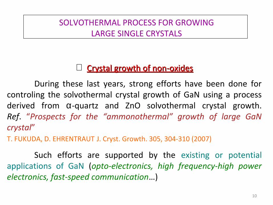
⇒ Crystal growth of non-oxidesCrystal growth of non-oxides
During these last years, strong efforts have been done for controling the solvothermal crystal growth of GaN using a process derived from α-quartz and ZnO solvothermal crystal growth.Ref. “Prospects for the “ammonothermal” growth of large GaN crystal”T. FUKUDA, D. EHRENTRAUT J. Cryst. Growth. 305, 304-310 (2007)
Such efforts are supported by the existing or potential applications of GaN (opto-electronics, high frequency-high power electronics, fast-speed communication…)

SOLVOTHERMAL PROCESS and CRYSTAL GROWTH
→ The crystal growth of materials as nano-particlesThe crystal growth of materials as nano-particles..
As the size is reduced to the nanometer range, the material exhibits specific properties due to quantization effects
[H. GLEITER Mater. Sci. Program. 33, 233 (1989),
Y. XIA et al. Advanced Materials 15, 353 (2003)]
In such a case the morphology plays an important role In such a case the morphology plays an important role ((0D0D,,1D,2D)1D,2D)
12
New Trends in Solvothermal Crystal Growth Processes
THE SOLVOTHERMAL PROCESSES ANDTHE CRYSTAL GROWTH AT THE NANOSCALE
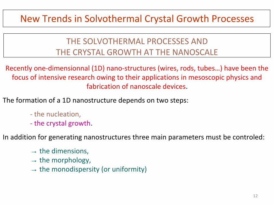
Recently one-dimensionnal (1D) nano-structures (wires, rods, tubes…) have been the focus of intensive research owing to their applications in mesoscopic physics and
fabrication of nanoscale devices.
The formation of a 1D nanostructure depends on two steps:
- the nucleation,- the crystal growth.
In addition for generating nanostructures three main parameters must be controled:
→ the dimensions,→ the morphology,→ the monodispersity (or uniformity)
13
THE SOLVOTHERMAL PROCESSES ANDTHE CRYSTAL GROWTH AT THE NANOSCALE
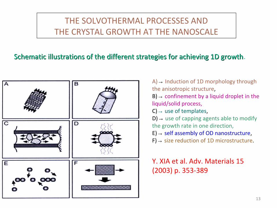
Schematic illustrations of the different strategies for achieving 1D growthSchematic illustrations of the different strategies for achieving 1D growth.
A)→ Induction of 1D morphology through the anisotropic structure,B)→ confinement by a liquid droplet in the liquid/solid process,C)→ use of templates,D)→ use of capping agents able to modify the growth rate in one direction,E)→ self assembly of OD nanostructure,F)→ size reduction of 1D microstructure.
Y. XIA et al. Adv. Materials 15 (2003) p. 353-389


CONCLUSIONS
• To open a route through new « soft chemical processes»
Kinetically controlled for stabilizing metastable systems.• To help the synthesis of specific structures using templates.• To control the nucleation/ crystal growth processes for the
preparation of nanocrystallites well defined in size and morphology.
• To facilitate ,through the improvement of the chemical reactivity and the development of mild temperature conditions, the synthesis of hybrid nano-systems.
• Mass production of samples
CONCLUSIONS
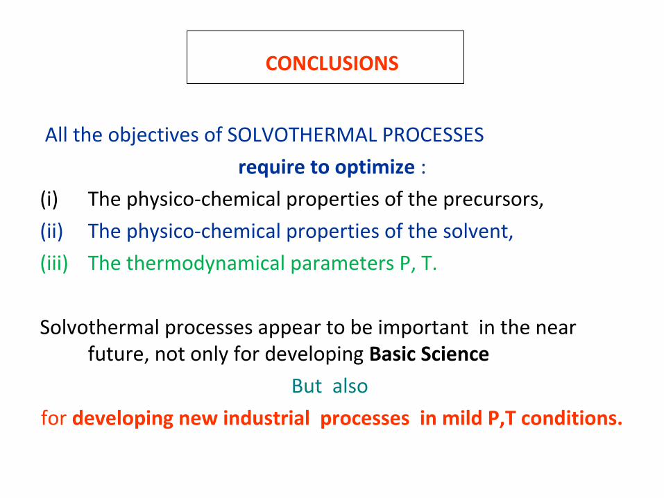
All the objectives of SOLVOTHERMAL PROCESSES
require to optimize :
(i) The physico-chemical properties of the precursors,
(ii) The physico-chemical properties of the solvent,
(iii) The thermodynamical parameters P, T.
Solvothermal processes appear to be important in the near future, not only for developing Basic Science
But also
for developing new industrial processes in mild P,T conditions.
SOLVOTHERMAL SYNTHESIS AND CHARACTERIZATION OF
SEMICONDUCTOR NANOPARTICLES OF CdSe AND CdSe/ZnS, CdSe/ZnSe AND CdSe/CdTe NANOCOMPOSITES
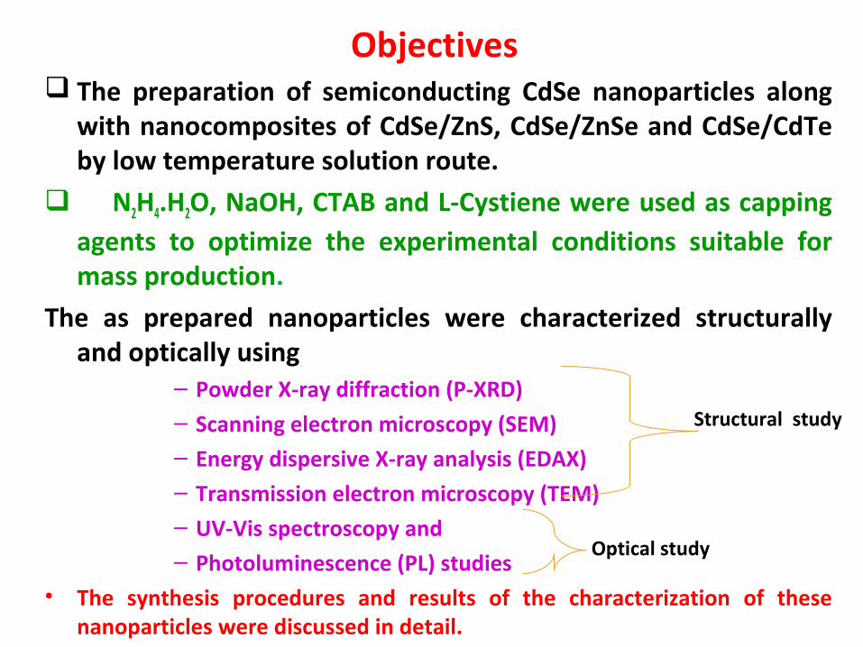
Objectives The preparation of semiconducting CdSe nanoparticles along
with nanocomposites of CdSe/ZnS, CdSe/ZnSe and CdSe/CdTe by low temperature solution route.
N2H4.H2O, NaOH, CTAB and L-Cystiene were used as capping agents to optimize the experimental conditions suitable for mass production.
The as prepared nanoparticles were characterized structurally and optically using
– Powder X-ray diffraction (P-XRD)– Scanning electron microscopy (SEM)– Energy dispersive X-ray analysis (EDAX)– Transmission electron microscopy (TEM)– UV-Vis spectroscopy and – Photoluminescence (PL) studies
• The synthesis procedures and results of the characterization of these nanoparticles were discussed in detail.
Structural study
Optical study
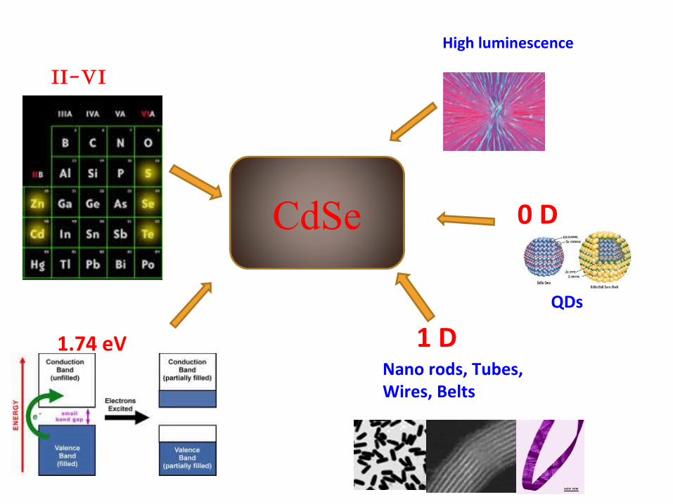
CdSe
II-VI
1.74 eV 1 D
0 D
Nano rods, Tubes, Wires, Belts
QDs
High luminescence
SYNTHESIS AND CHARACTERIZATION OF CdSe NANOPARTICLES
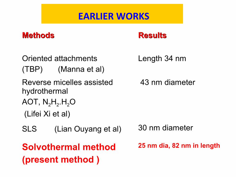
EARLIER WORKS
MethodsMethods Results Results
Oriented attachments(TBP) (Manna et al)
Length 34 nm
Reverse micelles assisted hydrothermal AOT, N2H2.H2O
(Lifei Xi et al)
43 nm diameter
SLS (Lian Ouyang et al) 30 nm diameter
Solvothermal method (present method )
25 nm dia, 82 nm in length
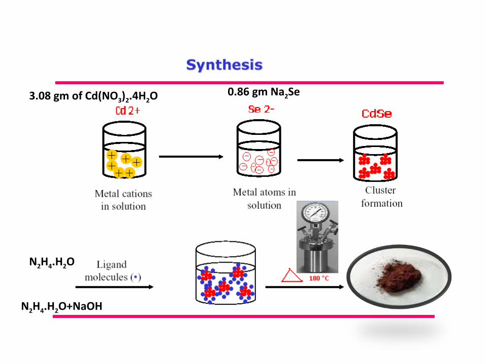
3.08 gm of Cd(NO3)2.4H2O0.86 gm Na2Se
N2H4.H2O
N2H4.H2O+NaOH

POWDER X-RAY DIFFRACTION PATTERN OF CdSe

a(Å) 4.218 Å
b(Å ) 4.218 Å
c(Å ) 6.887 Å
α(deg) 90 °
β(deg) 90 °
γ (deg) 120 °
Crystal system Hexagonal(Wurtzite) JCPDS 77-2307

TEM/HRTEM Analysis
Good shape with less pronounced stacking faults, with their measured values of mean diameter and length of 25 nm and
82 nm respectively.
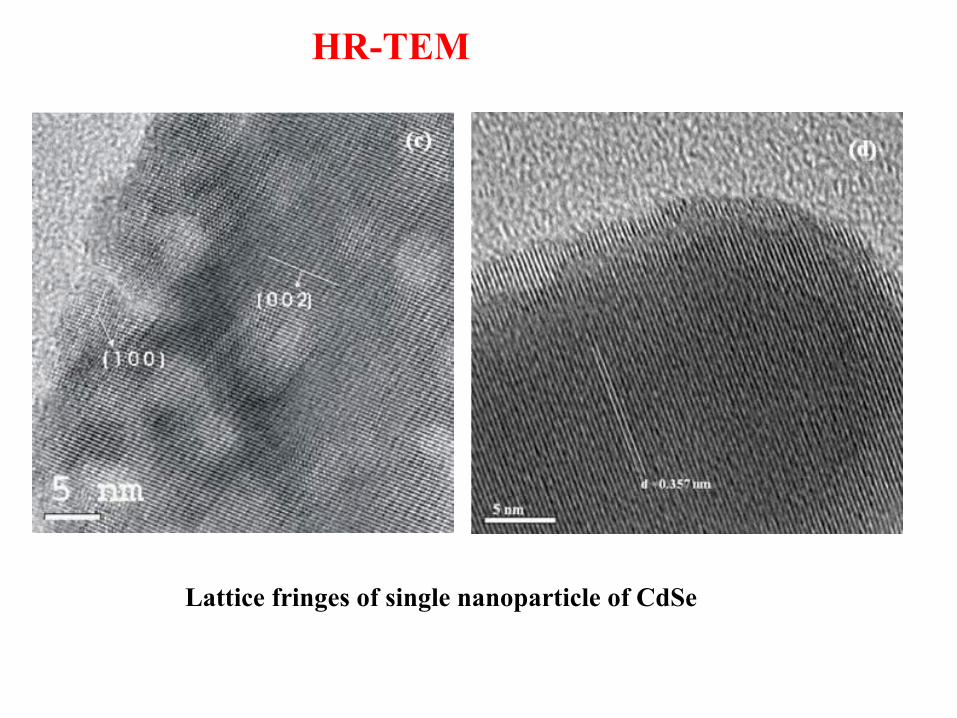
HR-TEM
Lattice fringes of single nanoparticle of CdSe

SAED & EDAX Pattern

CdSe Nanobelts (NBs)
Width of the nanobelts (NBs) 12-15 nm
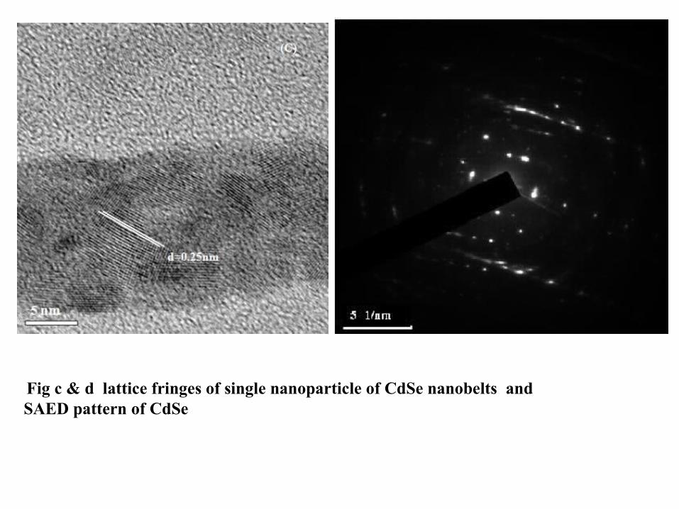
Fig c & d lattice fringes of single nanoparticle of CdSe nanobelts and SAED pattern of CdSe
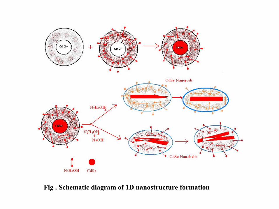
Fig . Schematic diagram of 1D nanostructure formation
2
2

200 400 600 800 1000 1200
2.0
2.5
3.0
3.5
4.0
4.5
Ab
sorp
tio
n (
a.u
)
Wavelength (nm)
CdSe NBs
UV-Vis-NIR Spectrophotometer
CdSe NBs the absorption edge (λe) 695 nmCdSe NRs the absorption edge (λe) 700 nm

Photoluminescence spectrum
The emission peak observed at 703 and 700 nm for NRs &NBs
Blue shift of 27 and 30 nm.
Bulk wurtzite CdSe 730 nm [Wang et al (1999)]
NRsNBs
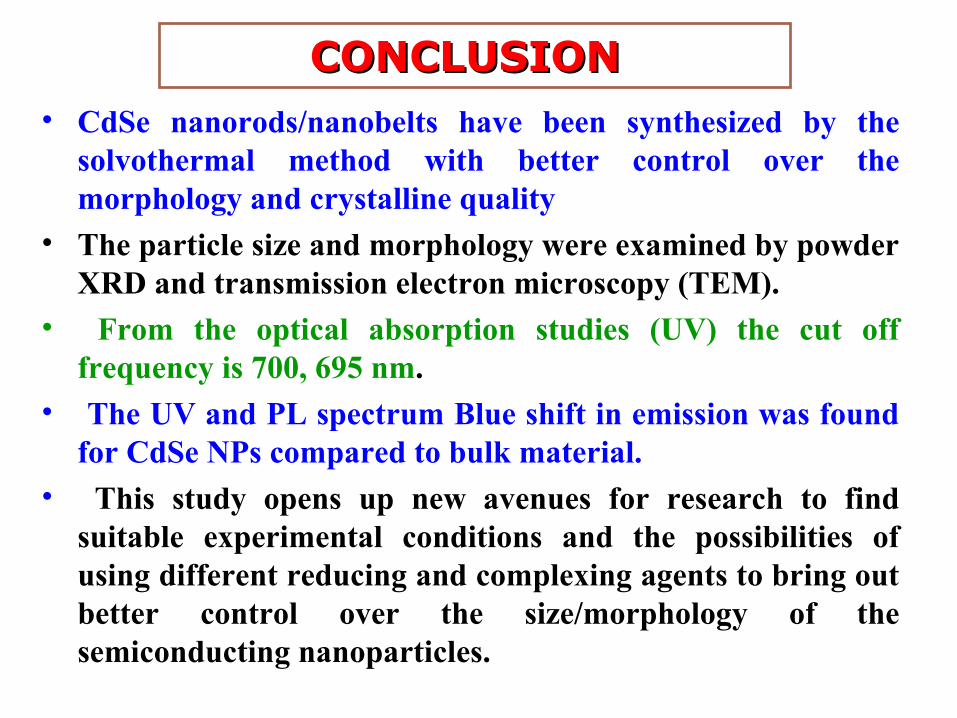
CONCLUSIONCONCLUSION • CdSe nanorods/nanobelts have been synthesized by the
solvothermal method with better control over the morphology and crystalline quality
• The particle size and morphology were examined by powder XRD and transmission electron microscopy (TEM).
• From the optical absorption studies (UV) the cut off frequency is 700, 695 nm.
• The UV and PL spectrum Blue shift in emission was found for CdSe NPs compared to bulk material.
• This study opens up new avenues for research to find suitable experimental conditions and the possibilities of using different reducing and complexing agents to bring out better control over the size/morphology of the semiconducting nanoparticles.
SYNTHESIS AND CHARACTERIZATION OF CdSe/ZnS NANOPARTICLES
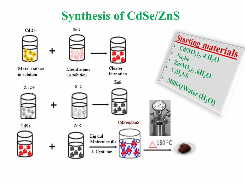
Synthesis of CdSe/ZnS
Results and Discussion
10 20 30 40 50 60 700
2000
4000
6000
8000
10000
12000
14000
(205)
Zn
S
(204)
Zn
S
(110)
Zn
S
(101)
Zn
S
(203)
Cd
Se
(201)
Cd
Se
(103)
Cd
Se
(110)C
dS
e
(102)
Cd
Se
(100)
Zn
S
(002)
Cd
Se
Inte
nsit
y (
arb
.un
it)
Two theeta
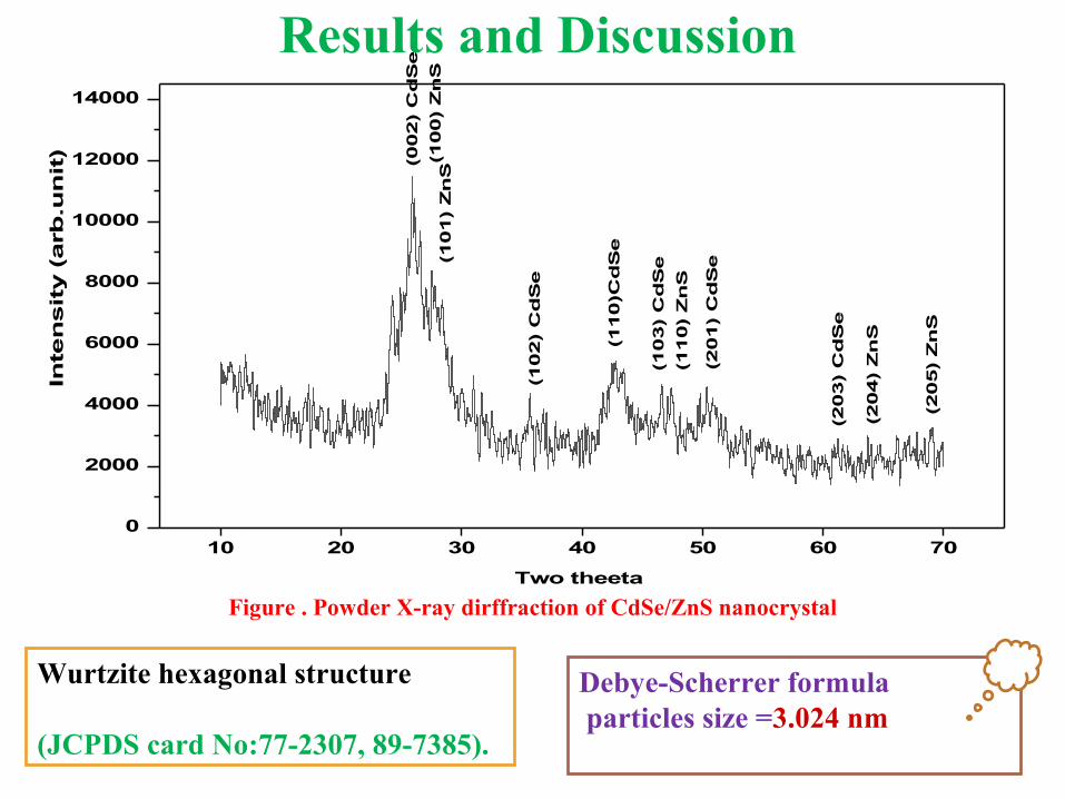
Wurtzite hexagonal structure
(JCPDS card No:77-2307, 89-7385).
Debye-Scherrer formula particles size =3.024 nm
Figure . Powder X-ray dirffraction of CdSe/ZnS nanocrystal

Figure. EDAX Spectrum of semiconductor nanocomposite with corresponding signals of Cd, Se, Zn and S
Scanning Electron Microscopy (SEM)
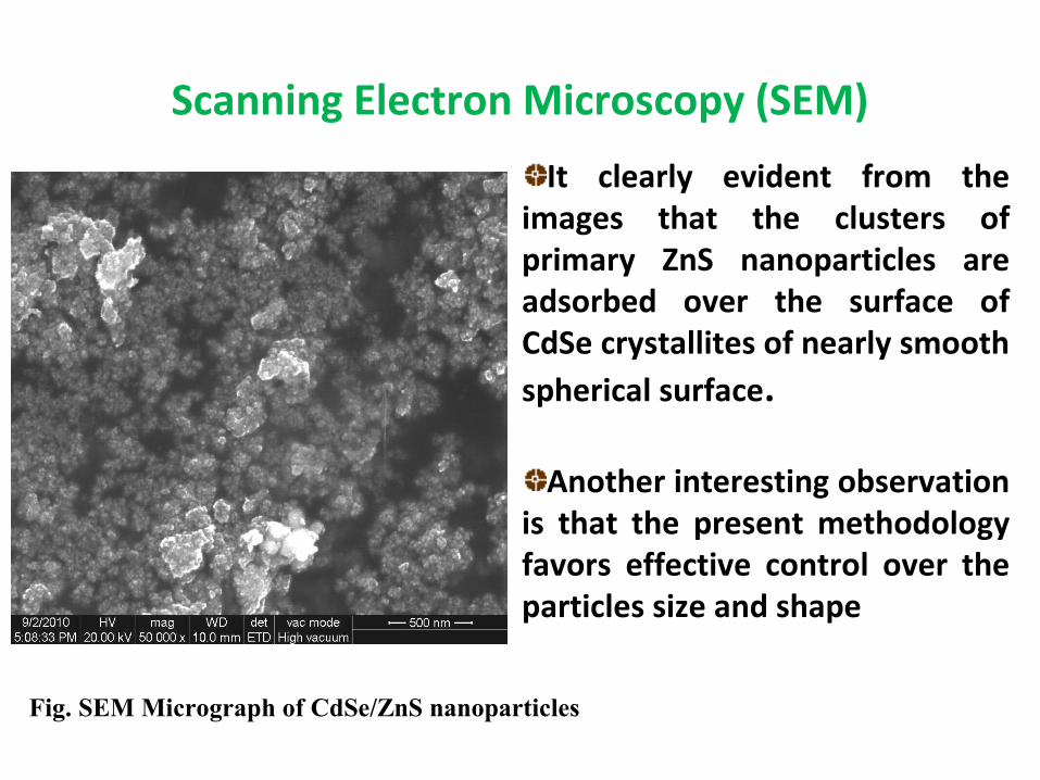
Fig. SEM Micrograph of CdSe/ZnS nanoparticles
It clearly evident from the images that the clusters of primary ZnS nanoparticles are adsorbed over the surface of CdSe crystallites of nearly smooth spherical surface.
Another interesting observation is that the present methodology favors effective control over the particles size and shape

Transmission Electron Microscopic Analysis (TEM)
2.0 2.5 3.0 3.5 4.0 4.5 5.00
10
20
30
40
50
No.
of p
arti
cles
Particles size (QDs)
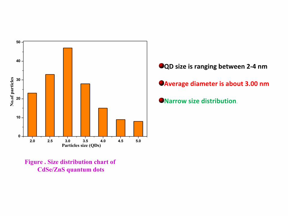
Figure . Size distribution chart of CdSe/ZnS quantum dots
QD size is ranging between 2-4 nm
Average diameter is about 3.00 nm
Narrow size distribution.

L-Cysetine play a vital role not only functions as a stabilizer in true system but also offers S atoms from its gradual decomposition in the later stage of the synthesis.
The ring pattern- selected area electron diffraction (SAED) is shown in figure which confirms the presence of QDs.
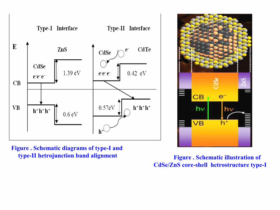
Figure . Schematic diagrams of type-I and type-II hetrojunction band alignment Figure . Schematic illustration of
CdSe/ZnS core-shell hetrostructure type-I

Optical Absorption Study
495 500 505 510 515 520 525 530 535 540 545
0.8
1.0
1.2
1.4
1.6
1.8
2.0
2.2
2.4
Ab
so
rpti
on
(a.u
)
Wavelength (nm)
Figure. UV-Vis absorption spectrum of CdSe/ZnS QDs
D = (1.6122 × 10⁻⁹) λ4 – (2.6575 × 10⁻⁶) λ3 + (1.6242 × 10⁻³) λ2 – (0.4277) λ + 41.57.Using the above formula the average nanoparticles diameter is found to be D=5.653 nm.
R=D/2= 2.8225 nm
An absorption peak for CdSe is expected at 716 nm.
There is a strong blue-shift in the absorption spectrum indicating that the particles must be smaller than the Bohr radius (aB) of exciton which is 5.4 nm for CdSe (Shriwas 2005).
The as prepared CdSe/ZnS QDs size is R=2.8 nm; the decreased (R<< aB) regime indicate the strong-quantum confinement effect (Babentson and Sizov 2008).
515 nm
500 510 520 530 540 550 560 570 580 590 6000.0
0.2
0.4
0.6
0.8
1.0
FWHM 15 nm
Inte
nsit
y(a
.u)
Wavelength (nm)
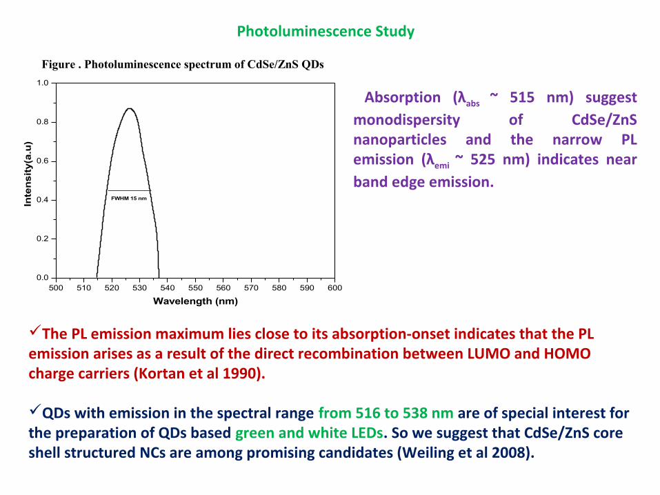
Figure . Photoluminescence spectrum of CdSe/ZnS QDs
Photoluminescence Study
The PL emission maximum lies close to its absorption-onset indicates that the PL emission arises as a result of the direct recombination between LUMO and HOMO charge carriers (Kortan et al 1990).
QDs with emission in the spectral range from 516 to 538 nm are of special interest for the preparation of QDs based green and white LEDs. So we suggest that CdSe/ZnS core shell structured NCs are among promising candidates (Weiling et al 2008).
Absorption (λabs ~ 515 nm) suggest monodispersity of CdSe/ZnS nanoparticles and the narrow PL emission (λemi ~ 525 nm) indicates near band edge emission.
Conclusion In the present work, efforts have been made to establish the feasibility of
NPs synthesis of amino acid capped CdSe/ZnS quantum dots. L-Cysteine plays three essential roles: Acts as a source for sulphide ions, as a growth moderator and as a stabilizer.
The size of CdSe / ZnS QDs was successfully controlled by environmental friendly solvent( L-Cystine).
A narrower particle size distribution upon ZnS shell growth and the control of the particle shape by symmetrically growing ZnS shell on CdSe core.
The better controlled size of QDs provides more efficient, more stable and luminescence spectral region used to generate green and white LEDs.
The as prepared CdSe/ZnS potentially lower toxity by non- toxic ZnS shell.

SYNTHESIS AND CHARACTERIZATION CdSe/ZnSe NANOCOMPOSITE

Synthesis of CdSe/ZnSe
Se 2-ZnSe
ZnSe
CdSe
CdSe CdSe/ZnSe
CTAB

Results and Discussion
10 20 30 40 50 60 700
20
40
60
80
100
120
140
(103) ZnSe(200) CdSe
(002) CdSe
(110) CdSe
(100) ZnSe
Inte
nsi
ty (
arb
.un
it)
Two theeta X-ray diffraction pattern of CdSe/ZnSe
nanocomposite
EDX line scanning spectrum of CdSe/ZnSe nanorod
The major diffracted planes (002), (100) and (200), (103) are indicating both CdSe and ZnSe nanocomposite hetrostructure are in wurtzite hexagonal phase.
This has been verified with JCPDS file numbers of CdSe (77-2307) and ZnSe (89-2940).
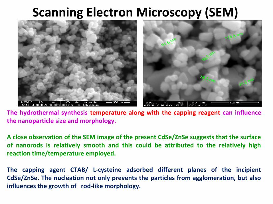
Scanning Electron Microscopy (SEM)
The hydrothermal synthesis temperature along with the capping reagent can influence the nanoparticle size and morphology.
A close observation of the SEM image of the present CdSe/ZnSe suggests that the surface of nanorods is relatively smooth and this could be attributed to the relatively high reaction time/temperature employed.
The capping agent CTAB/ L-cysteine adsorbed different planes of the incipient CdSe/ZnSe. The nucleation not only prevents the particles from agglomeration, but also influences the growth of rod-like morphology.
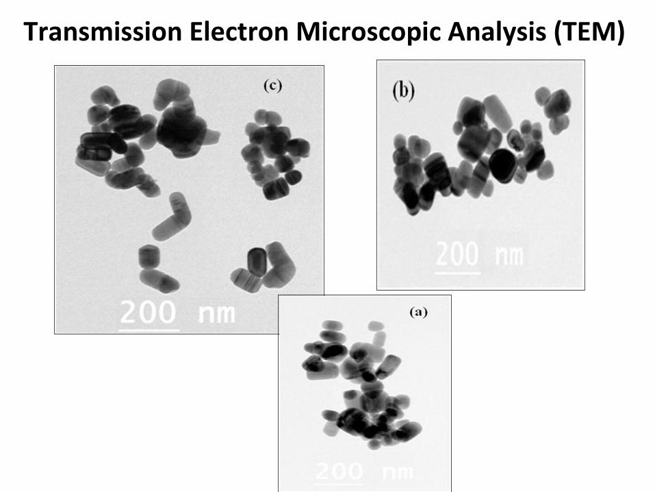
Transmission Electron Microscopic Analysis (TEM)

• The TEM photograph shows the presence of nanorods with a major population of prolonged nanorods as well as a minor population of spherical shape nanoparticles.
• The obtained nanorods have diameter in the range 50-70 nm and the length is 150-175 nm whereas the spherical shape nanocomposites were achieved within 40-50 nm diameters.
• It is clearly seen that as the time of growth increases, the spherical shape of the nanocomposite grow towards rod-like morphologies.
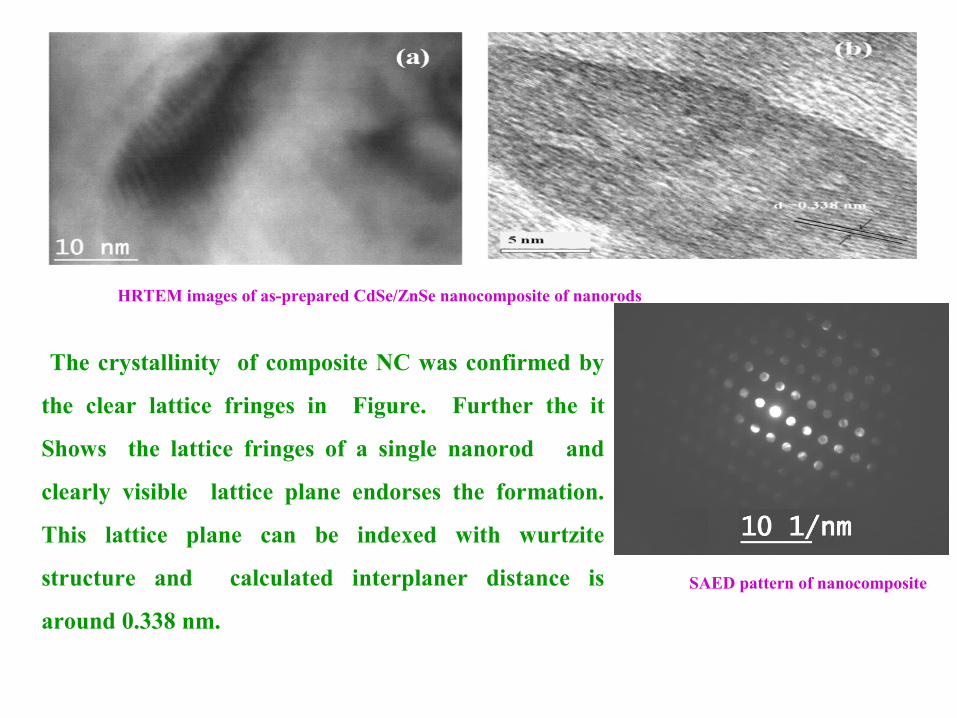
HRTEM images of as-prepared CdSe/ZnSe nanocomposite of nanorods
SAED pattern of nanocomposite
The crystallinity of composite NC was confirmed by
the clear lattice fringes in Figure. Further the it
Shows the lattice fringes of a single nanorod and
clearly visible lattice plane endorses the formation.
This lattice plane can be indexed with wurtzite
structure and calculated interplaner distance is
around 0.338 nm.
• we suggest that L-cysteine and CTAB proves the better surface passivation of the CdSe/ZnSe crystalline lattice under laboratory conditions.
• It is noted that thiol-capped NC containing amino groups can be easily used for the conjugation of two binary metals.
• During the growth process L-cysteine and CTAB plays an important role in the transformation of spherical to rod like morphology.
• The organic surfactant (CTAB) adsorbed by the coating of nanorods is essential to disperse and stabilize them in the solvent which could prevent their further agglomeration and oxidation .
200 400 600 800 1000
2.0
2.5
3.0
3.5
4.0
CdSe NRs
Ab
so
rpti
on
(a.u
)
Wavelength (nm)
480 490 500 510 520 530 540 550
0.6
0.8
1.0
1.2
1.4
1.6
1.8
2.0
2.2
2.4
Ab
so
rpti
on
(a.u
)
Wavelength (nm)
CdSe-ZnSe
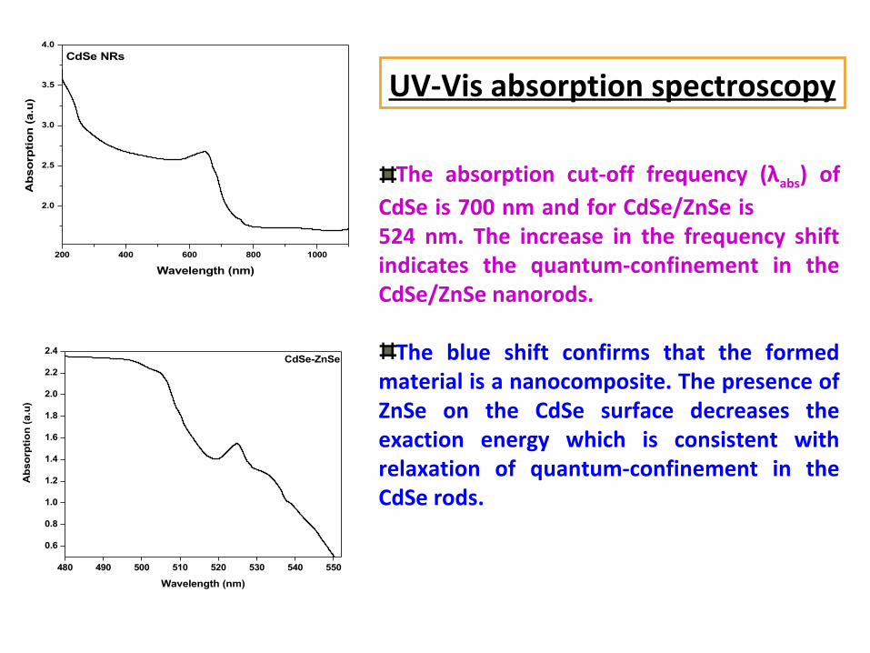
The absorption cut-off frequency (λabs) of CdSe is 700 nm and for CdSe/ZnSe is 524 nm. The increase in the frequency shift indicates the quantum-confinement in the CdSe/ZnSe nanorods.
The blue shift confirms that the formed material is a nanocomposite. The presence of ZnSe on the CdSe surface decreases the exaction energy which is consistent with relaxation of quantum-confinement in the CdSe rods.
UV-Vis absorption spectroscopy
Photoluminescence Study
02/06/15 05:08 AM
650 660 670 680 690 700 710 720
0.0
5.0x10⁶
1.0x10⁷
1.5x10⁷
2.0x10⁷
2.5x10⁷
Inte
nsi
ty (
Arb
.Un
it)
Wavelength (nm)
500 510 520 530 540 550 560 5700.0
0.5
1.0
1.5
2.0
2.5
3.0537 nm
520 nm
Inte
nsi
ty x
105 (
a.u
)
Wavelength (nm)
CdSe/ZnSe
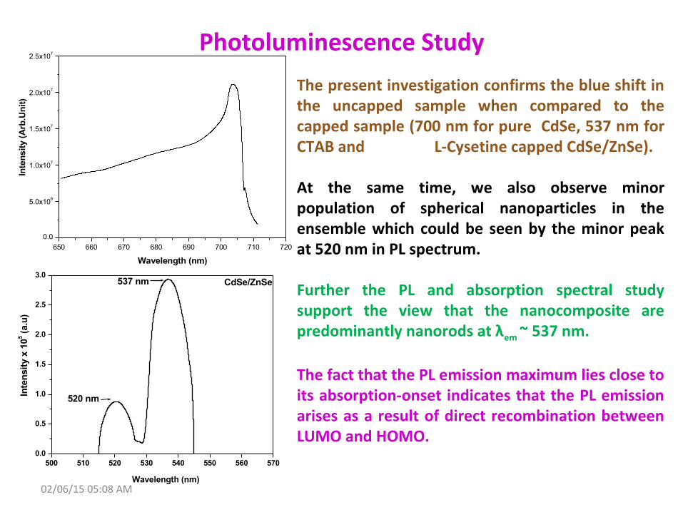
The present investigation confirms the blue shift in the uncapped sample when compared to the capped sample (700 nm for pure CdSe, 537 nm for CTAB and L-Cysetine capped CdSe/ZnSe).
At the same time, we also observe minor population of spherical nanoparticles in the ensemble which could be seen by the minor peak at 520 nm in PL spectrum.
Further the PL and absorption spectral study support the view that the nanocomposite are predominantly nanorods at λem ~ 537 nm. The fact that the PL emission maximum lies close to its absorption-onset indicates that the PL emission arises as a result of direct recombination between LUMO and HOMO.

CONCLUSION• The CdSe/ZnSe composite nanorods were successfully
synthesized by using bio capping agents L-Cysetine and CTAB.
• The wurtize-hexagonal morphology was verified by powder XRD and SAED Pattern. The EDA confirms the presence of Cd, Zn, Se metal in the as prepared nanorods.
• It has been demonstrated that the energy of the band-edge luminescence can be readily tuned by adding the ZnSe overlayer. This study opens up new avenues for research to synthesis L-Cysetine and CTAB bio-capsulated composite nanorods.
• This semiconducting nanorods has the potential for the application of solid-state lighting and molecular bio-imaging.
02/06/15 05:08 AM
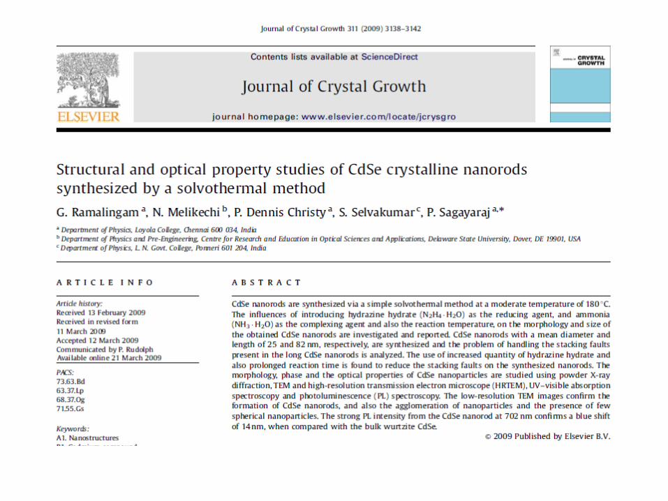
Synthesis and Characterization of CdSe/CdTe Nanorods
02/06/15 05:08 AM
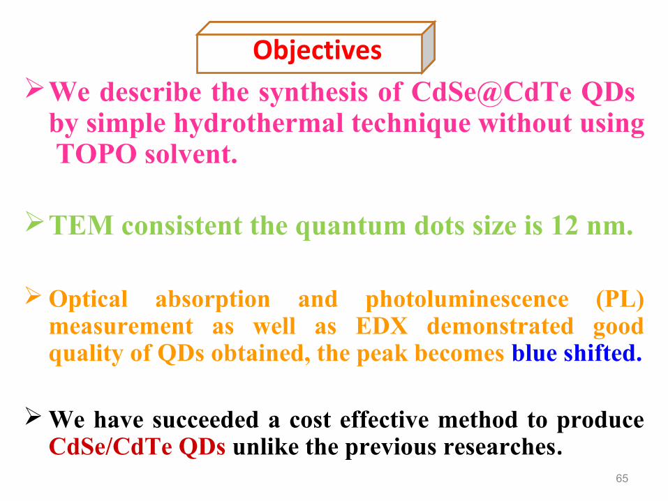
ObjectivesWe describe the synthesis of CdSe@CdTe QDs
by simple hydrothermal technique without using TOPO solvent.
TEM consistent the quantum dots size is 12 nm.
Optical absorption and photoluminescence (PL) measurement as well as EDX demonstrated good quality of QDs obtained, the peak becomes blue shifted.
We have succeeded a cost effective method to produce CdSe/CdTe QDs unlike the previous researches.
65
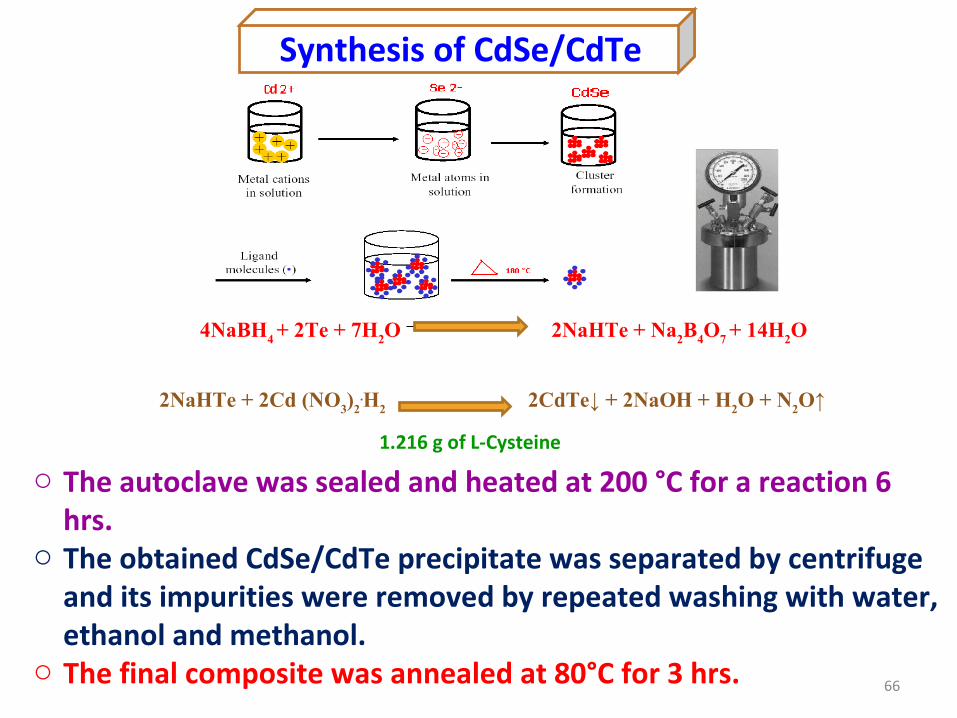
Synthesis of CdSe/CdTe
4NaBH4 + 2Te + 7H2O 2NaHTe + Na2B4O7 + 14H2O
2NaHTe + 2Cd (NO3)2.H2 2CdTe↓ + 2NaOH + H2O + N2O↑
o The autoclave was sealed and heated at 200 °C for a reaction 6 hrs.
o The obtained CdSe/CdTe precipitate was separated by centrifuge and its impurities were removed by repeated washing with water, ethanol and methanol.
o The final composite was annealed at 80°C for 3 hrs.
1.216 g of L-Cysteine
66

Results and Discussion
5 10 15 20 25 30 35 40 45 50 55 60 65 70500
510
520
530
540
550
560
570
580
590
600
Cd
Se (
002)
Cd
Se (
112)
Cd
Se (
101)C
dS
e (
002)
Cd
Te (
220)
Cd
Te (
211)
Cd
Te (
111)
Cd
Te (
100)
Inte
nsity (
arb
.un
it)
Two theeta
Fig. XRD pattern of CdSe/CdTe QDs
The diffraction peaks at 24.20°, 27.60°, 42.27° and 56.94° are assigned to the (002) (101) (112) and (002) planes of hexagonal phase. The intensity of four major peaks for cubic CdTe namely, (100) (111) (211) and (220) planes are positioned at 13.69°, 24.20°, 35.37° and 39.85° respectively. The diffraction peaks can be indexed to the mixed hexagonal and cubic CdSe/CdTe composite with L-Cystine capping legand.
The observed data are in good agreement with the literature values (JCPDS No: 89-3011 (CdTe) and 77-2304 (CdSe).
67
TEM Analysis
10 11 12 13 14 150
5
10
15
20
25
Nu
mb
ero
f P
arti
cles
Particles size distributation (nm)
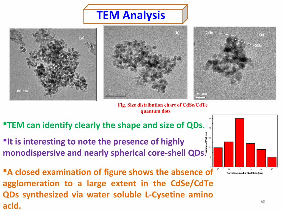
Fig. Size distribution chart of CdSe/CdTe quantum dots
TEM can identify clearly the shape and size of QDs.
It is interesting to note the presence of highly monodispersive and nearly spherical core-shell QDs.
A closed examination of figure shows the absence of agglomeration to a large extent in the CdSe/CdTe QDs synthesized via water soluble L-Cysetine amino acid.
68
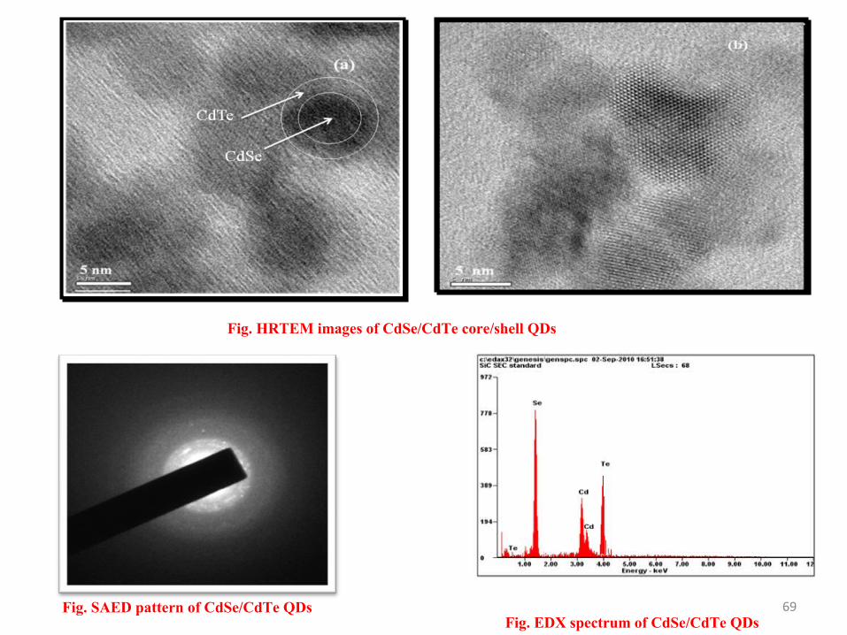
Fig. HRTEM images of CdSe/CdTe core/shell QDs
Fig. SAED pattern of CdSe/CdTe QDsFig. EDX spectrum of CdSe/CdTe QDs
69
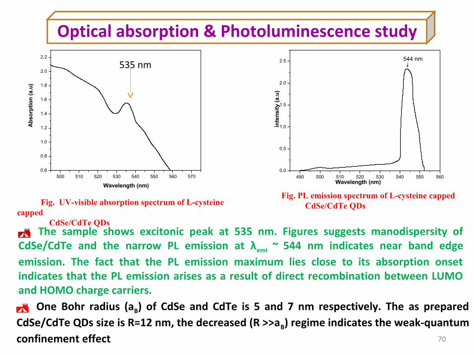
Optical absorption & Photoluminescence study
500 510 520 530 540 550 560 5700.6
0.8
1.0
1.2
1.4
1.6
1.8
2.0
2.2
Ab
sorp
tio
n (
a.u
)
Wavelength (nm)
490 500 510 520 530 540 550 5600.0
0.5
1.0
1.5
2.0
2.5 544 nm
inte
nsi
ty (
a.u
)
Wavelength (nm)
Fig. UV-visible absorption spectrum of L-cysteine capped
CdSe/CdTe QDs
Fig. PL emission spectrum of L-cysteine capped CdSe/CdTe QDs
The sample shows excitonic peak at 535 nm. Figures suggests manodispersity of CdSe/CdTe and the narrow PL emission at λemi ~ 544 nm indicates near band edge emission. The fact that the PL emission maximum lies close to its absorption onset indicates that the PL emission arises as a result of direct recombination between LUMO and HOMO charge carriers. One Bohr radius (aB) of CdSe and CdTe is 5 and 7 nm respectively. The as prepared CdSe/CdTe QDs size is R=12 nm, the decreased (R >>aB) regime indicates the weak-quantum confinement effect 70
535 nm

CONCLUSIONThe XRD and TEM results suggest that the size of spherical
CdSe/CdTe core shell QDs is 12 nm.
Further SAED pattern resembled the mixed hexagonal, cubic structure crystal system of core-shell nanoparticles are obtained .
The absorbance of characteristic QDs revealed the weak Quantum confinement effect of the charge carriers in the core shell crystals system.
The PL emission of the resulting type II QDs was found to be significantly higher than that of the CdTe/CdSe core/shell.
71
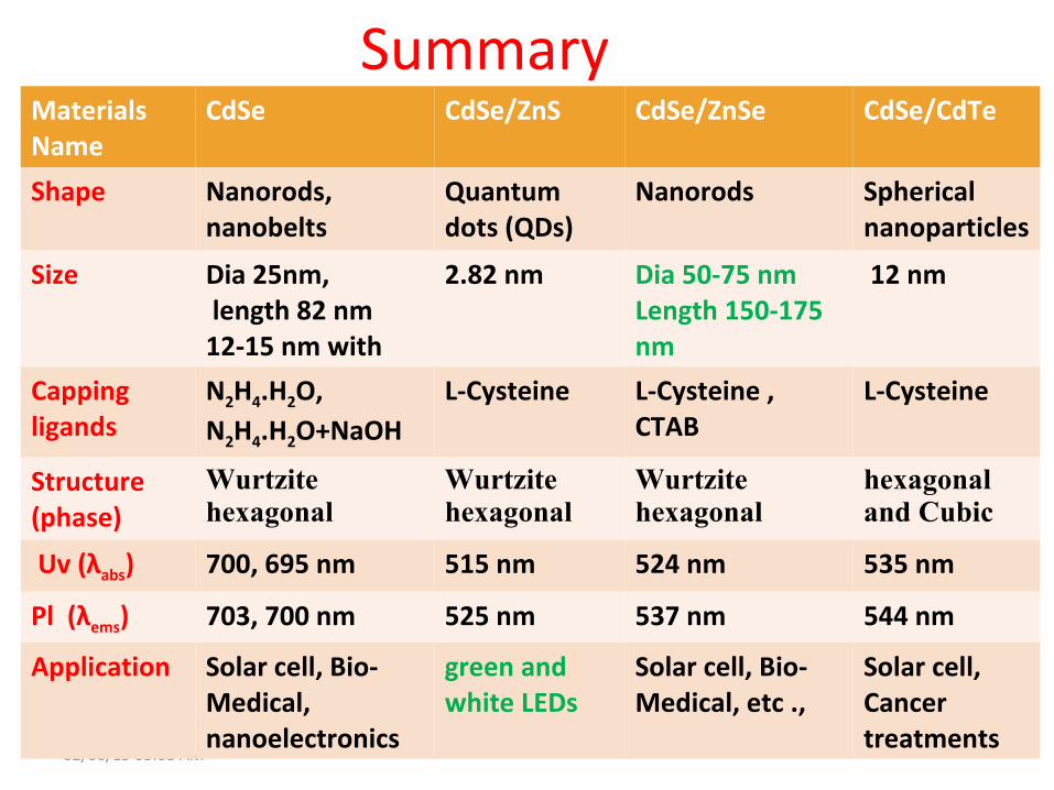
Summary
02/06/15 05:08 AM
Materials Name
CdSe CdSe/ZnS CdSe/ZnSe CdSe/CdTe
Shape Nanorods, nanobelts
Quantum dots (QDs)
Nanorods Spherical nanoparticles
Size Dia 25nm, length 82 nm12-15 nm with
2.82 nm Dia 50-75 nmLength 150-175 nm
12 nm
Capping ligands
N2H4.H2O, N2H4.H2O+NaOH
L-Cysteine L-Cysteine , CTAB
L-Cysteine
Structure (phase)
Wurtzite hexagonal
Wurtzite hexagonal
Wurtzite hexagonal
hexagonal and Cubic
Uv (λabs) 700, 695 nm 515 nm 524 nm 535 nm
Pl (λems) 703, 700 nm 525 nm 537 nm 544 nm
Application Solar cell, Bio-Medical, nanoelectronics
green and white LEDs
Solar cell, Bio-Medical, etc .,
Solar cell, Cancer treatments
Future work
Different synthesis routes, The preparation of thin films
Varying calcinations temperatures, pH, pressure,different concentrations of the involved surfactants /modifiers
Nanoparticles are to be coupled with quantum dots to fabricate QDs sensitized solar cell, nonlinear optical, optoelectronic devices and bio-medical labeling.


THANK YOU FOR YOUR ATTENTION.
Top Related