


Languages
Pages
Legal

Project Report On
Skin Response Meter
By:Joshi Dhruv (34)Gorakh Yash (25)Goswami Krunal (27)
B. Tech Semester V Electronics and Communication EngineeringNov - Dec 2010
Submitted to,Department of Electronics and Communication Engineering,
U. V. Patel College of EngineeringGanpat University, Kherva - 382 711

U.V.PATEL COLLEGE OF ENGINEERING
Nov – Dec 2010
C E R T I F I C A T E
T O W H O M S O E V E R I T M A Y C O N C E R N
This is to certify that Mr. Dhruv Joshi, Yash Gorakh and Krunal Goswami,
student of B. Tech Semester V (Electronics and Communication Engineering)
have completed Mini Project titled “Skin Response Meter” in the year 2010.
Mrs. Priyanka Patel HeadSign EC Department
INDEX
SR. NO. TOPIC
1. Abstract
2. Acknowledgment
3. Parts List
4. Circuit Diagram
5. Circuit Description
6. Parts Description
7. Application
8. Conclusion
9. Bibliography

ABSTRACT
Human skin offers some resistance to current and voltage. This resistance changes with the emotional state of the body. The circuit proposed here measures changes in the skin resistance following changes in the mental state.
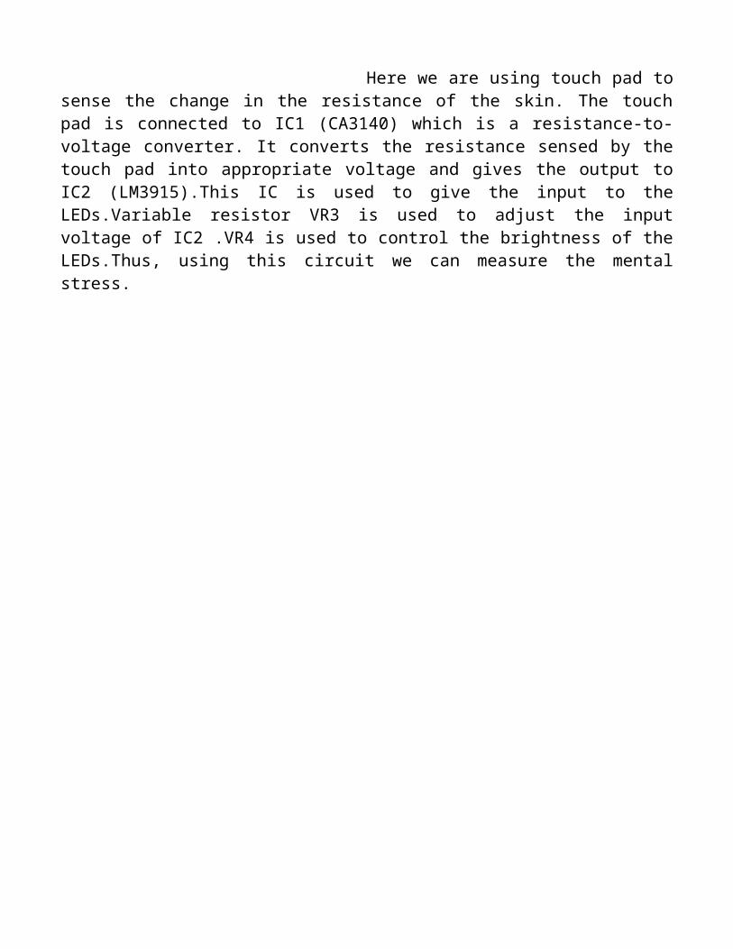
Here we are using touch pad to sense the change in the resistance of the skin. The touch pad is connected to IC1 (CA3140) which is a resistance-to-voltage converter. It converts the resistance sensed by the touch pad into appropriate voltage and gives the output to IC2 (LM3915).This IC is used to give the input to the LEDs.Variable resistor VR3 is used to adjust the input voltage of IC2 .VR4 is used to control the brightness of the LEDs.Thus, using this circuit we can measure the mental stress.
ACKNOWLEDGEMENT
Project of “Skin Response Meter” is used to perform desired tasks in unstructured environments without continuous guidance. We have designed this project under the guidance of madam Priyanka Patel who has made great efforts in making our project successful. This project is very creative in electronic world.
Yours sincerely,
Joshi Dhruv
Gorakh Yash
Goswami Krunal

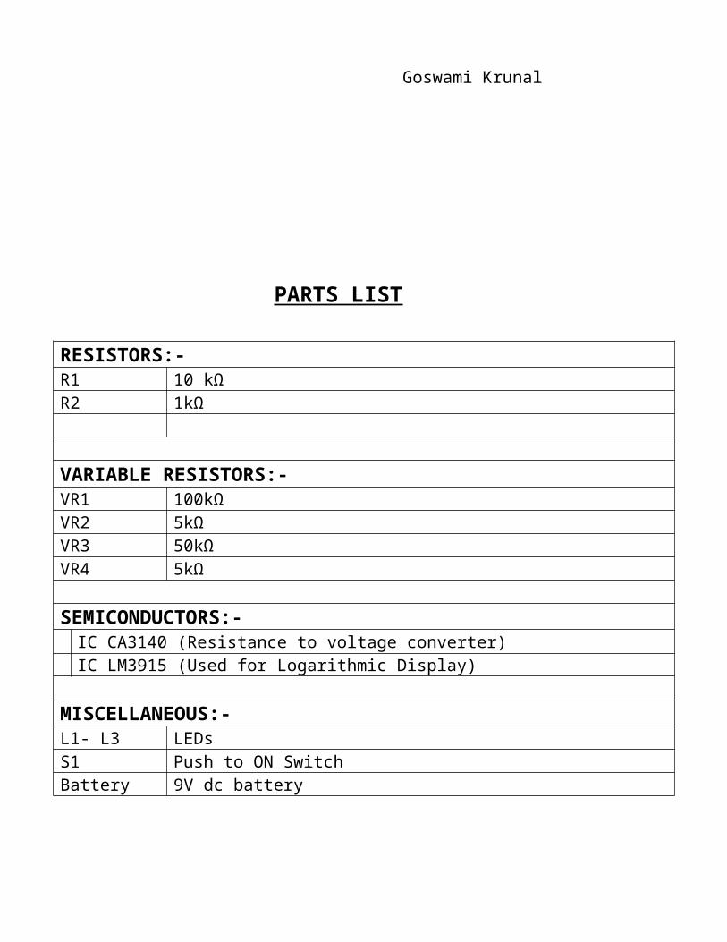
PARTS LIST
RESISTORS:-R1 10 kΩR2 1kΩ
VARIABLE RESISTORS:-VR1 100kΩVR2 5kΩVR3 50kΩVR4 5kΩ
SEMICONDUCTORS:- IC CA3140 (Resistance to voltage converter)IC LM3915 (Used for Logarithmic Display)
MISCELLANEOUS:-L1- L3 LEDs S1 Push to ON SwitchBattery 9V dc battery
CIRCUIT DIAGRAM
CIRCUIT DESCRIPTION
Description: In the relaxed state, the resistance offered by the skin is as high as 2 mega-
ohms or more, which reduces to 500 kilo-ohms or less when the emotional stress is too high. The reduction in skin resistance is related to increased blood flow and permeability followed by the physiological changes during high stress. This increases the electrical conductivity of the skin.
The circuit uses a sensitive amplifier to sense variations in the skin resistance. IC CA3140 (IC1) is designed as a resistance-to-voltage converter that outputs varying voltage based on the skin’s conductivity. It is wired as an inverting amplifier to generate constant current to skin in order to measure the skin resistance.
The inverting input (pin 2) of IC1 is connected to ground (through preset VR1) and one of the touch plates, while the non-inverting input (pin 3) is grounded directly. The output from IC1 passes through current-limiting resistor R1 to the second touch plate.
R1 act as a feedback resistor along with the skin when the touch plates make contact with the skin. So the gain of IC1 depends on the feedback provided by R1 and the skin. In the inverting mode of IC1, a positive input voltage to its pin 2 through the feedback network makes its output low.
If the skin offers very high resistance in the relaxed state, input voltage to pin 2reduces and the output remains high. Thus the gain of IC1 varies depending on the current passing through the skin, which, in turn, depends on the skin response and emotional state. In the standby state, touch plates are free. As there is no feedback to IC1, it gives a high output (around 6 volts).
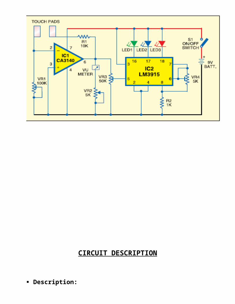
When the touch plates are shorted by the skin, the feedback circuit completes and the output voltage reduces to 4 volts or less depending on the resistance of the skin. For easy visual observation, an LED display is also included. IC LM3915 (IC2) is used to give a logarithmic display through LED indications. It can sink current from pin 18 to pin 10 with each increment of 125 mill volts at its input pin 5. Using VR3 you can adjust the input voltage of IC2, while using VR4 you can control the brightness of the LEDs.
If you are stressed or have ill feeling, skin resistance decreases and the blue LED lights up followed by the red LED along with a deflection of the meter towards the lower side. In short, the red LED and zero meter reading indicate you are stressed, and the green LED and high meter reading indicate you are relaxed.
PARTS DESCRIPTION
IC CA3140:
Features
• MOSFET Input Stage- Very High Input Impedance (ZIN) -1.5TΩ (Typ)- Very Low Input Current (Il) -10pA (Typ) at ±15V- Wide Common Mode Input Voltage Range (VlCR) - Can beSwung 0.5V below Negative Supply Voltage Rail
- Output Swing Complements Input Common Mode Range
• Directly Replaces Industry Type 741 in Most Applications
• Pb-Free Plus Anneal Available (RoHS Compliant)
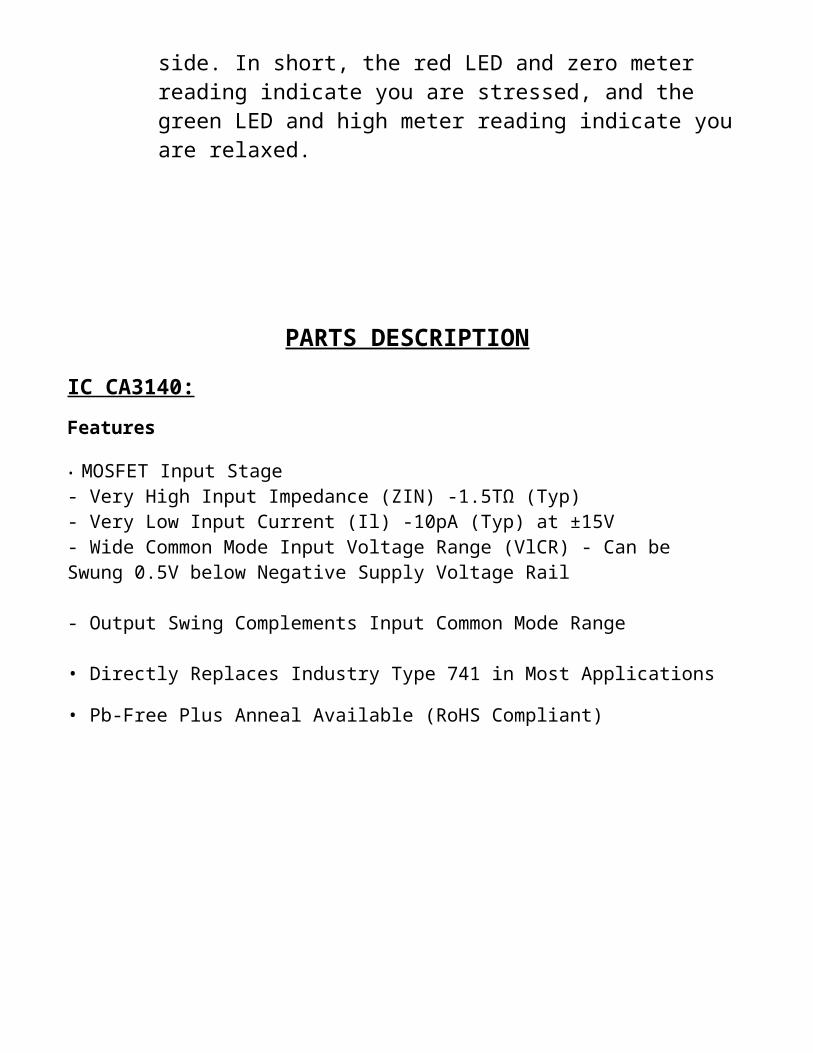
PINS
1. Offset Nullo can be effected with a 10kΩ potentiometer connected across
Terminals 1 and 5 and with its slider arm connected to Terminal4. 2. INV. INPUT
o Inverted input
3. NON-INV. INPUTo Non-inverting input
4. V-o Negative input
5. V+o Positive input
6. Strobeo Strobe input
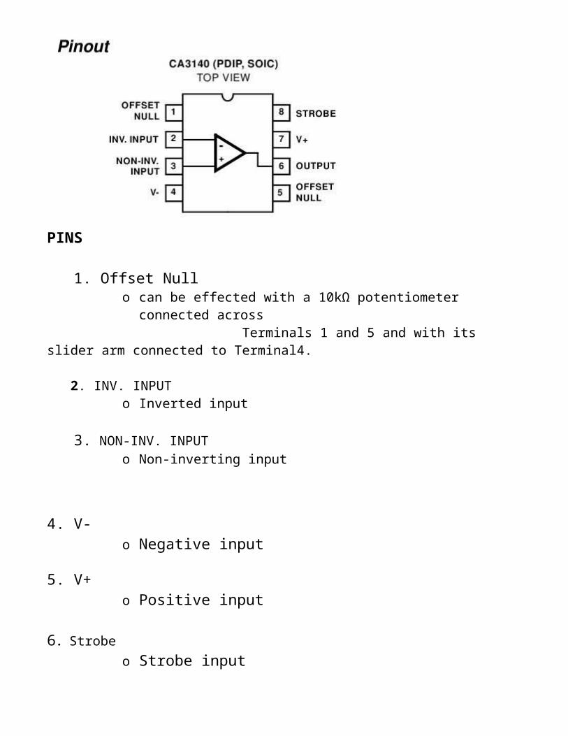
DescriptionThe CA3140A and CA3140 are integrated circuit operational amplifiers that combine the advantages of high voltage PMOS (Power MOSFET) transistors with high voltage bipolar transistors on a single monolithic chip. The CA3140A and CA3140 BiMOS operational amplifiers feature gate protected MOSFET (PMOS) transistors in the input circuit to provide very high input impedance, very low input current, and high speed performance. The CA3140A and CA3140 operate at supply voltage from 4V to 36V (either single or dual supply). These operational amplifiers are internally phase compensated to achieve stable operation in unity gain follower operation, and additionally, have access terminal for a supplementary external capacitor if additional frequency roll-off is desired. Terminals are also provided for use in applications requiring input offset voltage nulling. The use of PMOS field effect transistors in the input stage results in common mode input voltage capability down to 0.5V below the negative supply terminal, an important attribute for single supply applications. The output stage uses bipolar transistors and includes built-in protection against damage from load terminal short circuiting to either supply rail or to ground.
BLOCK DIAGRAM:
Applications
• Ground-Referenced Single Supply Amplifiers in Automobile and Portable Instrumentation• Sample and Hold Amplifiers• Long Duration Timers/Multivibrators(seconds-Minutes-Hours)• Photocurrent Instrumentation• Peak Detectors• Active Filters• Comparators• Power Supplies
IC LM3915
Features
3 dB/step, 30 dB range Drives LEDs, LCDs, or vacuum fluorescents Bar or dot display mode externally selectable by user Expandable to displays of 90 dB Internal voltage reference from 1.2V to 12V Operates with single supply of 3V to 25V Inputs operate down to ground Output current programmable from 1 mA to 30 mA Input withstands ±35V without damage or false outputs Outputs are current regulated, open collectors Directly drives TTL or CMOS The internal 10-step divider is floating and can be
referenced to a wide range of voltages
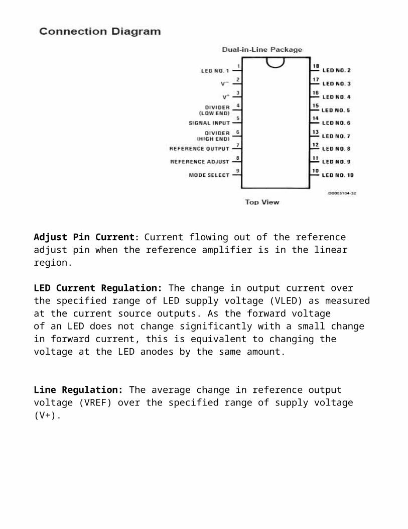
Adjust Pin Current: Current flowing out of the reference adjust pin when the reference amplifier is in the linear region.
LED Current Regulation: The change in output current over the specified range of LED supply voltage (VLED) as measured at the current source outputs. As the forward voltageof an LED does not change significantly with a small change in forward current, this is equivalent to changing the voltage at the LED anodes by the same amount.
Line Regulation: The average change in reference output voltage (VREF) over the specified range of supply voltage (V+).
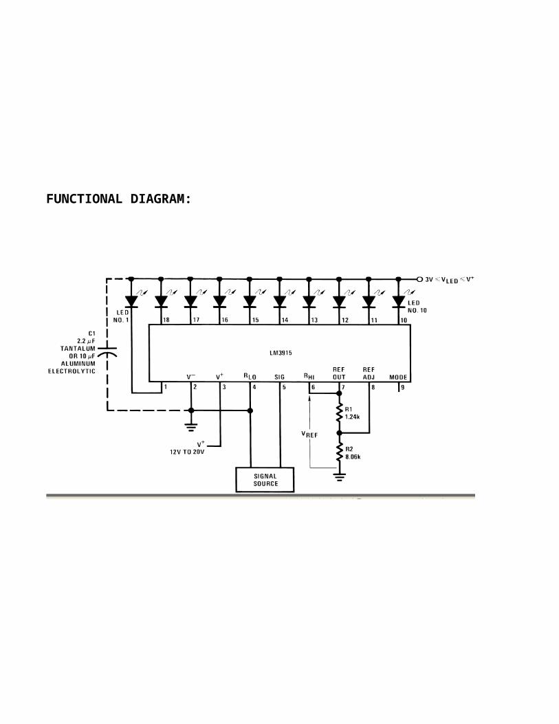
FUNCTIONAL DIAGRAM:
Description:
The simplified LM3915 functional diagram is included to give the general idea of the circuit’s operation. A high input impedance buffer operates with signals from ground to 12V, and is protected against reverse and overvoltage signals. The signal is then applied to a series of 10 comparators; each of which is biased to a different comparison level by the resistor string. the resistor string is connected to the internal 1.25V reference voltage. In this case, for each 3 dB that the input signal increases, a comparator will switch on another indicating LED. This resistor divider can be connected between any 2 voltages, providing that they are at least 1.5V below V+ and no lower than V−.

The LM3915 is relatively low-powered itself, and since any number of LEDs can be powered from about 3V, it is a very efficient display driver. Typical standby supply current (all LEDs OFF) is 1.6 mA. However, any reference loading adds 4 times that current drain to the V+ (pin 3) supply input. For example, an LM3916 with a 1 mA reference pin load (1.3k) would supply almost 10 mA to every LED while drawing only 10 mA from its V+ pin supply. At full-scale, the IC is typically drawing less than 10% of the current supplied to the display
Applications
LED Display Rectifier Circuits Precision Full-wave Average Detector Precision Full-wave Peak Detector Cascaded ICs for multiple 60db Displays Liquid Crystal Displays Audio Power Meters

APPLICATIONS
Measurement of very less currents (in pA)
Helpful in detection of stress & its prognosis in medicine
Can become a part of bigger system used in medical applications
Extremely effective tool for neurologists
CONCLUSION
From our Skin Response Meter, we conclude that, it is a versatile platform that allows developments of various applications. It works on a unique phenomenon of change in the skin resistance with the mental stress. It measures the resistance and gives the level of stress as an outcome.Thus; it can be accommodated into any larger device for medical applications.
BIBLOGRAPHY
www.electronics4u.com
www.efymag.com
www.national.com
www.intersil.com
Top Related