


Languages
Pages
Legal

Polymer Nanomechanical Cantilever Sensors with Novel Electrical Transduction Schemes for
Bio/chemical Sensing Submitted in partial fulfilment of the requirements
for the degree of
Doctor of Philosophy
by
Seena.V (Roll Number: 06407601)
Supervisors:
Prof. V. Ramgopal Rao
Prof. Soumyo Mukherji
Department of Electrical Engineering
INDIAN INSTITUTE OF TECHNOLOGY, BOMBAY
2011
ii
Dedicated to
My Parents, In-Laws, Husband Dr. Pradeep Kumar, Son Jagdeep and
Brother Sanith
A humble offering at the lotus feet of my AMMA,
Sadguru Sri Mata Amritanandamayi Devi


iv
Declaration
I declare that this written submission represents my ideas in my own words and where
others’ ideas or words have been included, I have adequately cited and referenced the original
sources. I also declare that I have adhered to all principles of academic honesty and integrity
and have not misrepresented or fabricated or falsified any idea/data/fact/source in my
submission. I understand that any violation of the above will be cause for disciplinary action
by the institute and can evoke penal action from the sources which have thus not been
properly cited or from whom proper permission has not been taken when needed.
_________________________________
Seena.V
Roll No. 06407601
Date: ________________
\
v
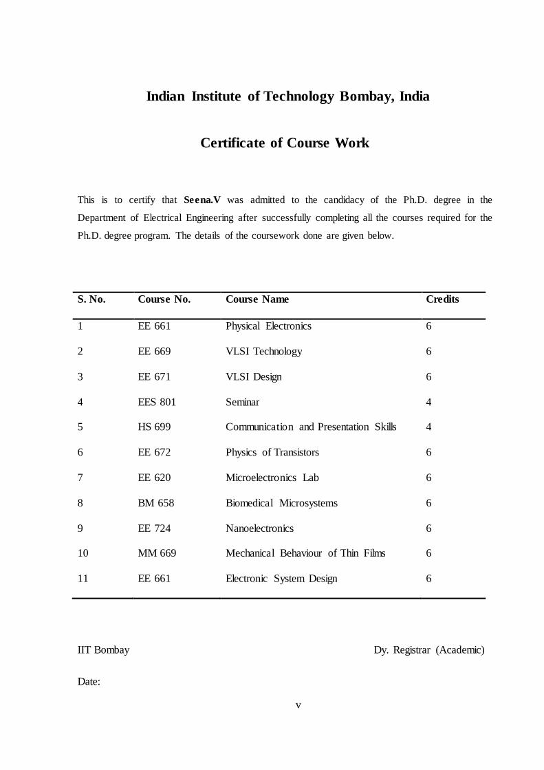
Indian Institute of Technology Bombay, India
Certificate of Course Work
This is to certify that Seena.V was admitted to the candidacy of the Ph.D. degree in the
Department of Electrical Engineering after successfully completing all the courses required for the
Ph.D. degree program. The details of the coursework done are given below.
S. No. Course No. Course Name Credits
1 EE 661 Physical Electronics 6
2 EE 669 VLSI Technology 6
3 EE 671 VLSI Design 6
4 EES 801 Seminar 4
5 HS 699 Communication and Presentation Skills 4
6 EE 672 Physics of Transistors 6
7 EE 620 Microelectronics Lab 6
8 BM 658 Biomedical Microsystems 6
9 EE 724 Nanoelectronics 6
10 MM 669 Mechanical Behaviour of Thin Films 6
11 EE 661 Electronic System Design 6
IIT Bombay Dy. Registrar (Academic)
Date:

vi
Acknowledgments
I am highly indebted to my guide Prof. V. Ramgopal Rao, for his constant and
valuable guidance at every stage of my work. It was through him that I got inducted to the
field of microelectronics. His positive approach in solving problems, and the faith and
confidence he has shown on me, motivated me in pursuing my Ph.D.
I am grateful to my co-guide Prof. Soumyo Mukherji for his support and timely
suggestions in the course of my research work. He has been a constant source of
encouragement throughout my Ph.D. I am extremely thankful to him for the guidance he gave
me in writing thesis.
I owe my sincere gratitude to Prof. Prita Pant for all the guidance and support she gave
me in characterizing the mechanical behavior of films and devices. I also owe my sincere
thanks Prof. Prakash.R.Apte for boosting my interest in systematically analyzing and solving
problems and for the valuable suggestions he gave me during the final stages of my work.
My sincere acknowledgement to Prof. Rudra Pratap, Department of Mechanical
Engineering, Indian Institute of Science, and Bangalore, India for the LDV characterization
experiments on polymer cantilevers and microaccelerometers performed at IISC under his
guidance.
I express my sincere thanks to my Research progress Committee members Prof.
D.Bahadur and Prof. Anilkumar for their acceptance to be in my panel and having spent their
valuable time in reviewing my annual progress reports and for providing valuable inputs.
I take this opportunity to acknowledge the partial funding received from the
Department of Information Technology, Government of India, through the Centre of
Excellence in Nanoelectronics. I sincerely thank Tata Consultancy Services, India for the
fellowship for my doctoral studies at IIT Bombay. I sincerely acknowledge Prof. Dinesh. K.
Sharma for his support through TCS fellowship scheme.
I hereby thank the staff and students of Centre for Excellence in Nanoelectronics for
their constant and efficient services. I thank Prof. Pinto for his support in terms of guidance
vii
for staff and students of CEN in maintaining the fabrication facility. I wish to acknowledge
the Nanoindenter facility and Central SPM facility of IIT Bombay.
I acknowledge to the project support received from Department of Science and
Technology, Govt. of India for developing the explosive sensors using microcantilevers. The
project helped in bringing focus to my research in developing low cost polymer
microcantilevers for explosive sensing. I thank Dr Pramod Soni from TBRL India for
providing the calibrated TNT vapour generator for the explosive vapour experiments.
I would also like to thank my colleagues Prajakta, Prasenjit, Anukool, Avil,
Ravishankar, Nidhi, Akash, Ramesh, Rohit, Harshil, Bijesh and Nikhil for all kinds of co-
operation, support and discussions during experimental work. I appreciate Prajakta for her
contributions to microaccelerometer developments. My special thanks to Ramesh for all his
help for pentacene depositions using his optimized parameters. I thank Karuna for all her
support during nanoindentation experiments. I take this opportunity to thank my friends,
Naveen, Rajashree and Harshil for proof reading my thesis. I owe my sincere thanks to
Naveen who has been very sincere in helping me by discussing the results. My special thanks
to Shweta Deora who has been a wonderful friend right from beginning of my Ph.D. I would
like to thank Ms. Tanvi Shelatkar, Ms. Arti, Mr. Santosh, Ms. Madhu, Ms. Vaishali and others
in EE Dept., IRCC and administrative staff of IIT Bombay for their timely help in various
official matters.
I am indebted to my in-laws, who came to support me and my husband during really
hard times of our Ph.D. I am ever indebted to my parents, who have always been my source
of motivation for studies throughout my life. I render my appreciation to my mother and
mother in-law who did their best at different times to support me by taking care of my son.
My heartfelt appreciation is extended to my husband, Dr. Pradeep Kumar, who motivated me
to join for Ph.D. and constantly supported me in stressful times during my research work.
With his experiences in doing Ph.D. at IIT Bombay, he could guide me in many aspects
throughout my Ph.D. My son, Master Jagdeep, has been a perennial source of enthusiasm and
cheer at all times through his constant inquiries and innocent playful tricks.
Seena.V
viii
Abstract
Bio/chemical sensing applications in the areas such as environmental monitoring,
healthcare, biomedical technology, clinical analysis and food processing demand fast, hand-
held, easy to use, inexpensive and highly sensitive methods for detection of very low levels of
chemical or biological substances. The demand for miniaturized high throughput sensors
supported by advancements in micro electro mechanical systems (MEMS) and
nanotechnology had led to the development of simple, versatile and promising class of
sensors known as “nanomechanical cantilever based bio/chemical sensors”.
The nanomechanical cantilever based bio/chemical sensors translate molecular
interactions into nanomechanical motions that can be measured by different external (optical)
and integrated transduction (electrical) techniques. Self-sensing microcantilevers with
integrated electrical transduction mechanism overcome the practical limitation with optical
microcantilevers pertaining to the field deployment of sensors. The conventional
microcantilever sensors are mostly silicon-based with their design and performances limited
by their high stiffness structures. Polymers such as SU-8, on the other hand have a much
lower Young’s modulus compared to silicon based materials which can be exploited for
achieving improvement in sensitivity. The cost of fabrication of polymer devices are known
to be much lower compared to conventional silicon microfabrication processes. This research
work focuses on the development of ultra-sensitive and cost effective polymer
nanomechanical cantilever sensors with novel integrated electrical transduction schemes for
bio/chemical sensing applications.
The first part of this research work aimed at the development of an optimized and
highly sensitive SU-8 nanomechanical cantilever bio/chemical sensor with embedded polymer
nanocomposite of SU-8 and Carbon Black (CB) as the piezoresistive layer. The optimization
targeted improving its electrical, mechanical and transduction characteristics. An optimum
concentration of CB in SU-8 in the range of 8–9 vol. % was arrived at by performing
systematic mechanical and electrical characterizations of the SU-8/CB nanocomposite.
Mechanical characterization of SU-8/CB nanocomposite thin films was performed using the
nanoindentation technique with an appropriate substrate effect analysis. Piezoresistive SU-8
nanocomposite microcantilevers having an optimum CB concentration were fabricated with a
ix
design aimed at surface stress measurements and reduced fabrication process complexity.
With the optimized material formulations and fabrication processes, stress free SU-8
nanocomposite microcantilevers with an average beam thickness of just 3 μm were achieved
with an improved sensitivity, low device variability and a low noise level. The devices were
characterized for their mechanical, electromechanical and noise performances. The devices
exhibited the highest surface stress sensitivity of 7.6 ppm (mN m−1) −1 among polymer
piezoresistive microcantilevers reported in literature and the noise characterization results
support their suitability for biochemical sensing applications.
A chemical sensing application for polymer nanocomposite microcantilevers for the
detection of explosive vapours has been developed for the first time. These polymer devices
functionalized with 4-MBA were found to be suitable for detection of explosives like TNT
and RDX. The controlled experiments that had been carried out for detection of different
concentrations of TNT vapours verified their potential to detect TNT vapour concentrations
down to less than 6 ppb with an approximate sensitivity value of 1 mV/ppb of TNT. The
sensor was found to be reusable for multiple sensing operations and sensitivity and response
time were found to be adequate for detection of explosive vapours even in ambient.
The final part of this research work introduces an ultra-sensitive SU-8 nanomechanical
cantilever sensor with integrated electrical transduction using a strain sensitive organic field
effect transistor (OFET) inside SU-8 cantilever structure. This novel device was named as
‘Organic CantiFET’. A novel and simple fabrication process was developed that yielded low
cost Organic CantiFET chip. Organic CantiFET devices were characterized to evaluate their
mechanical, electrical, noise and electromechanical performances and thereby benchmark
them with other available microcantilever sensors. These devices exhibit higher deflection
and surface stress sensitivities (15.6 ppm/nm and 400 ppm compared to that of SU-8
nanocomposite cantilevers that has been presented in the initial parts of this research work.
The characterization results proved their candidature as efficient and cost effective
biochemical sensors having a minimum detectable surface stress in the range of 0.18 mN/m.
Key words: polymer microcantilever, polymer nanocomposite,SU-8 nanocomposite, SU-
8/CB nanocomposite, nanoindentation, Young’s modulus, spring constant, SU-8, carbon
black, explosive detection, OFET, pentacene, nanomechanical cantilever, Organic CantiFET,
SU-8 dielectric
x
Table of Contents
1.1 Introduction to the topic ..................................................................................22
1.2 Motivation .........................................................................................................3
1.3 Microcantilevers as bio/chemical sensors-Literature review............................5
1.3.1 Sensing modes and principles.............................................................5
1.3.2 Microcantilever materials .................................................................10
1.3.3 Transduction principles ....................................................................11
1.3.4 Polymeric piezoresistive microcantilevers .......................................18
1.3.5 Applications of microcantilever as bio/chemical sensors.................21
1.3.6 Microcantilevers for detection of explosive vapours........................23
1.4 Objectives and scope of the work ...................................................................25
1.5 Thesis Organization ........................................................................................28
2.1 Introduction .....................................................................................................30
2.2 SU-8 material properties and processing ........................................................31
2.3 Single layer SU-8 microcantilevers for optical transduction ..........................34
2.3.1 Design of single layer SU-8 microcantilevers ..................................34
2.3.2 Fabrication process development for SU-8 microcantilevers...........37
2.3.3 Challenges in fabrication ..................................................................41
2.3.4 Optimized fabrication process for SU-8 microcantilevers ...............43
2.3.5 Characterization ................................................................................45
2.3.6 Application in explosive vapour detection .......................................47
Acknowledgments ................................................................................ vi
Abstract.............................................................................................. viii
List of figures ..................................................................................... xiii
List of tables ........................................................................................xxiChapter 1 Introduction and Literature Review ................................. 22
Chapter 2 SU-8 Microcantilevers for Optical Transduction.............. 30
xi
2.4 Summary .........................................................................................................51
3.1 Introduction .....................................................................................................53
3.2 SU-8/CB nanocomposite thin film preparation and patterning ......................54
3.3 Electrical characterization: Percolation study on SU-8/CB nanocomposite...60
3.4 Development of SU-8/CB nanocomposite microcantilevers ..........................62
3.4.1 Fabrication process ...........................................................................64
3.4.2 Characterization ................................................................................68
3.4.3 Shortcomings and scope for improvement .......................................69
3.5 Optimization of SU-8/CB nanocomposite microcantilevers ..........................70
3.5.1 Characterization of dispersion of Carbon black in SU-8 ..................70
3.5.2 Nanoindentation for mechanical characterization of SU-8/CB
nanocomposites.................................................................................73
3.5.3 Electrical characterization of SU-8/CB nanocomposite:
Conduction mechanism and temperature dependence......................78
3.5.4 Design and fabrication of SU-8/CB nanocomposite
microcantilevers with improved sensor performance .......................82
3.5.5 Mechanical characterization: Spring constant and resonant
frequency measurements ..................................................................88
3.5.6 Electromechanical characterization: Sensitivity ...............................92
3.5.7 Noise characterization ......................................................................93
3.6 Summary .........................................................................................................96
4.1 Introduction .....................................................................................................98
4.2 Explosive Vapour Experiments ......................................................................99
Chapter 3 Polymer Nanocomposite Microcantilever Sensor with Integrated Electrical Transduction ..................................................... 53
Chapter 4 Detection of Explosive Vapours using Polymer
Nanocomposite Microcantilevers ........................................................ 98
xii
4.2.1 Controlled experiments with a flow cell on PCB ...........................105
4.3 Effect of humidity on microcantilever response ...........................................107
4.4 Summary .......................................................................................................110
5.1 Introduction ...................................................................................................112
5.2 Organic CantiFET device design and development......................................114
5.2.1 Material selection............................................................................114
5.2.2 Organic CantiFET device designs ..................................................122
5.2.3 Process integration for organic CantiFETs .....................................123
5.3 Characterization of Organic CantiFET .........................................................128
5.3.1 Electrical characterization ..............................................................129
5.3.2 Mechanical characterization ...........................................................129
5.3.3 Electromechanical characterization ................................................132
5.3.4 1/f noise characterization ................................................................136
5.4 Summary .......................................................................................................139
Chapter 5 Polymer nanomechanical sensor with integrated OFET for electrical transduction....................................................................... 112
Chapter 6 Conclusion and future recommendations ....................... 140
Appendix A ....................................................................................... 145
Appendix B ....................................................................................... 147
Appendix C ....................................................................................... 152
Appendix D ....................................................................................... 158
Appendix E ....................................................................................... 162
References164
List of publications............................................................................ 175
List of figures
Figure 1.1 Schematic representation of selectivity in bio/chemical sensors..................... 2
Figure 1.2 Principle of microcantilever based bio/chemical sensor.................................. 3
Figure 1.3 Microcantilever operation modes [12]............................................................. 6
Figure 1.4 Lateral view of a beam subjected to surface stress changes of Δσ1 and Δσ2 leading to a bending with constant radius of curvature of R. The dotted line corresponds to the neutral axis [14] ...................................................................... 7
Figure 1.5 Schematic depiction of (a) chemisorption of straight-chain thiol molecules on a gold coated cantilever. (b) analyte-induced cantilever deformation due to the swelling of thick analyte permeable coating during analyte interaction. (c) analyte- induced cantilever deformation in the case of a nanostructured surface coating [15]. .......................................................................................................... 8
Figure 1.6 Schematic of (A)"optical lever" readout that is commonly used to measure the deflection of microcantilever probes in standard AFM [8] (B) interferometric readout [39] ......................................................................................................... 12
Figure 1.7 (A) A schematic of a simplified piezoresistive microcantilever model consisting of single layer of structural material with thickness h and a piezoresistor with thickness → 0. (B) Schematic of the microcantilever in Wheatstone bridge configuration. ....................................................................... 15
Figure 1.8 (A) Schematic of the interaction between probe and target molecules on an embedded MOSFET microcantilever [50] .......................................................... 16
Figure 1.9 SU-8 microcantilever with Au as strain gauge (A) Schematic of the device chip (B) Optical micrograph of the microcantilever with integrated meander-type Au resistor [34]............................................................................................ 18
Figure 1.10 Optical image of a micromachined SU-8 cantilever with integrated SU-8/carbon piezoresistor (Length = 200 m, Width = 200 m and thickness = 7 m) [57] .............................................................................................................. 19
Figure 2.1 Typical photolithographic processing sequence for microfabrication of SU-8 structures. (1) Dehydration baking step for removing the moisture on the sample surface (2) SU-8 resist is spun onto a sample (3) Prebake on a hotplate for evaporating the solvent. (4) UV-light exposure through a mask. (5) Post
xiv
exposure bake for completion of crosslinking process (6) Development in SU-8 developer to remove the non-cross- linked areas in SU-8 ................................... 33
Figure 2.2 Resonant frequency and spring constant as function of length of the microcantilever .................................................................................................... 36
Figure 2.3 Schematic of SU-8 microcantilever die for optical transduction (A) Single cantilever die (B) Schematic of the cantilever die attached to the SU-8 frame. . 37
Figure 2.4 Schematic of fabrication process flow for SU-8 microcantilevers (A) Sacrificial layer (B) Structural layer SU-8 for the microcantilever (C) Thick SU-8 for anchor and frames of microcantilever die (D) Release of the microcantilever devices attached to frame. ......................................................... 37
Figure 2.5 (A) SU-8 patterns on substrate indicating the stress lines (B ) and (C) SEM micrograph of the fabricated SU-8 microcantilever after release from the substrate............................................................................................................... 41
Figure 2.6(A)160 µm thick SU-8 structure before hard bake. Stress indicated in corners (B) The sample after hard bake. Stress lines got vanished after hard bake......... 44
Figure 2.7 SU-8 microcantilevers fabricated after optimization process (A) SU-8 frames holding arrays of SU-8 microcantilevers. These devices were coated with gold. (B) Optical micrograph of one of the microcantilevers (C) SEM micrograph indicating the stress free nature of the microcantilevers ..................................... 45
Figure 2.8 Frequency response of gold coated SU-8 microcantilever ............................ 46
Figure 2.9 Simulated data of resonant frequency with scaling of length of the SU-8 microcantilever coated with Cr/Au. Inset : Mesh model for the microcantilever structure. .............................................................................................................. 47
Figure 2.10 Experimental setup for explosive vapour experiment (A) Schematic of the setup (B) Explosive vapour generator ................................................................. 49
Figure 2.11 Response of the microcantilever to TNT vapour stream generated at 65oC with a flow rate of 30 SCCM .............................................................................. 50
Figure 2.12 (A) Conceptual diagram of microcantilever coated with benzene thiol (eg. 4-MBA) receptors on the gold side and undergoing compressive stress and bending due to interaction with aromatic gas (B) Interaction between DNT and 4 MBA leading to compressive stress in the gold film (C) interaction between DNT and 4-MBA at SAM grain boundaries leading to compressive strain in gold film [97] ...................................................................................................... 51
Figure 3.1 (A) Optical micrograph of SU-8/CB nanocomposite with lot of CB clusters on a pattern of Au on silicon dioxide. (B) SEM micrograph showing a CB cluster in SU-8..................................................................................................... 56
xv
Figure 3.2 Optical micrograph of photo-lithographically patterened SU-8/CB with 5 CB vol. % (A) before and (B) after ultra-sonication clean step in IPA..................... 57
Figure 3.3 SU-8/CB (8.4 vol%) strips patterned using different UV exposure doses (A) 204 mJ/cm2 (B) 408 mJ/cm2 (C) 530 mJ/cm2 (D) SEM image of SU-8/CB strip with 530 mJ/cm2. .......................................... 57
Figure 3.4 Microfabrication processing steps for SU-8/CB nanocomposite .................. 58
Figure 3.5 Thickness and RMS roughness as a function of CB concentration ............... 58
Figure 3.6 (A & B) AFM topographical images of SU-8/CB Composite films (A) 6 vol% (B) 7.4 vol% (C) SEM micrograph of SU-8/CB composite with 8 vol.%59
Figure 3.7 Percolation theory applied to conductive composites. The formation of the first complete particle linkage occurs at Vc that resulting in a sharp decrease in resistivity [101] ................................................................................................... 60
Figure 3.8 Percolation characteristics of SU-8/CB composite........................................ 61
Figure 3.9 Optical micrograph (20X) of SU-8/CB film on SU-8 for different CB concentration showing the density of conductive filler network. ....................... 62
Figure 3.10 Schematic of SU-8/CB nanocomposite microcantilever die ....................... 63
Figure 3.11 Fabrication process flow for SU-8/CB nanocomposite microcantilevers (1) Sacrificial or release layer (2) First layer of SU-8 (3) Cr/Au for contact pads (4) Ti/Au contact wire (5)SU-8/CB nanocomposite layer (6) encapsulating SU-8 (7) Thick SU-8 die base (8) Release of cantilever die from the substrate ....... 66
Figure 3.12 Photographs and micrographs of fabricated polymer nanocomposite microcantilever devices at different stages of fabrication (A) Processed 2" silicon wafer after final lithography step (B) Released devices soaked in IPA after etching of Cr layer on contact pads (C) Released and dried SU-8 frames holding the microcantilever devices (D and E) SEM and optical micrograph of on of the microcantilever die............................................................................... 67
Figure 3.13 Electromechanical characterization plots of two SU-8 nanocomposite microcantilevers with different resistances ......................................................... 68
Figure 3.14 Dispersion characterization results from DLS (A & B) Size distribution of CB for samples prepared with energy of sonication of 3kJ and 0.6 kJ. (C) Mean diameter of carbon black as a function of duration of sonication. ...................... 71
Figure 3.15 . SEM mage of SU-8/CB Composite films prepared with sonication energy of (A) 0.6 kJ (B) 3 kJ in pulse ............................................................................. 72
Figure 3.16 SEM micrograph of SU-8/CB nanocomposite pattern with reduced line edge roughness .................................................................................................... 72
xvi
Figure 3.17 Typical load vs. depth of indentation plot obtained in nanoindentation experiment ........................................................................................................... 73
Figure 3.18 Load versus indentation depth for different loads. Inset: Scanned image of a set of indents in SU-8 .......................................................................................... 75
Figure 3.19 Young’s modulus and hardness of SU-8 as a function of indentation depth. The discontinuous line indicates the indentation depth of 10% of film thickness ............................................................................................................................. 76
Figure 3.20 (A) Young’s modulus of SU-8 as a function of indentation depth after modified King’s analysis. (B)Young’s Modulus of SU-8/CB composite as a function of CB Vol %. Here all the samples were indented with Pmax = 450 N ............................................................................................................................. 77
Figure 3.21 (A) I-V characteristics for SU-8/CB composites with 4.9 CB vol.% and 9.4 CB vol.% along with the theoretical curve fit (B) Value of power term ‘n’ and exponential term ‘B’ for different CB resistors .................................................. 78
Figure 3.22 Electrical characterization of nanocomposite resistors showing the variability in resistance as a function of CB concentration................................. 80
Figure 3.23 Temperature dependent resistance of SU-8/CB composites with CB concentration of (A) 6 vol. % (B) 7.8 vol. % ...................................................... 81
Figure 3.24 (A) Contact current mechanism in polymer PTC composite (B) Tunneling current mechanism in polymer [102] .................................................................. 81
Figure 3.25 Device design schematic. (A) Planar schematic (B).Cross sectional schematic of SU-8 cantilever with embedded SU-8/CB composite. .................. 83
Figure 3.26 Fabrication process flow (1) First layer of SU-8 (2) Cr/Au for contacts (3) SU-8/CB composite layer (4) encapsulating SU-8 (5) Thick SU-8 die base (6) Release of cantilever die from the substrate........................................................ 84
Figure 3.27 SU-8/CB resistor patterns on “V” shaped and “U” shaped cantilever areas after lithography process 4 .................................................................................. 85
Figure 3.28 (A) Photograph of the processed wafer after the final lithographic step. Arrays of polymer devices attached to the dummy substrate just before the release can be seen (B) optical micrograph of one of the devices on the wafer. (C) Arrays of polymer nanocomposite microcantilever device chips after release process (D) SEM image of one of the device chips containing 4 cantilevers. .... 86
Figure 3.29 Modified fabrication process flow (1) Sacrificial layer (2) First layer of SU-8. But not developed (3) SU-8/CB composite layer before development(4)SU-8/CB nanocomposite layer and SU-8 layer 1 after development with sonication
xvii
(5) Cr/Au for contacts (6) encapsulating SU-8 (7) Thick SU-8 die base (8) Release of cantilever die from the substrate........................................................ 87
Figure 3.30 Load and unload segment of indentation on cantilever ............................... 89
Figure 3.31 Load displacement characteristics of SU-8 nanocomposite microcantilever obtained from nanoindenter. Insets: (1)Schematic of measurement.(2) Optical image indicating the place of indentation on the SU-8 nanocomposite microcantilever .................................................................................................... 90
Figure 3.32 Frequency plot from Laser Doppler Vibrometer (A) “U” shaped cantilever(B) “V” shaped cantilever ................................................................... 91
Figure 3.33 Electromechanical characterization plot. Inset : I-V characteristics of the polymer nanocomposite microcantilever with different bending conditions for a voltage span of 100 mV (200 data points). ......................................................... 92
Figure 3.34 Noise measurement scheme for polymer nanocomposite microcantilever . 94
Figure 3.35 (A) Noise spectral density of SU-8/CB nanocomposite microcantilevers with 2 different concentrations (B) Noise spectral density at different bias voltage for devices with 8.4 CB vol%................................................................. 94
Figure 4.1 (A) Wheatstone bridge circuit indicating the microcantilever positions (B) Block diagram schematic of ADS1232REF board to which the bridge output is fed ...................................................................................................................... 100
Figure 4.2 Microcantilever response recorded during deflection using calibrated micromanipulator .............................................................................................. 101
Figure 4.3 Schematic of the experimental set up for explosive vapour experiments.... 101
Figure 4.4 (A & B) PTFE gas flow cell (FC) incubating the microcantilever PCB that is connected to DC bridge circuit, all inside a shielded enclosure. ADS1232 REF circuit from TI can be seen here (C & D) Microcantilever PCB and a microcantilever die (E) Complete experimental setup. VG: Vapour generator ; FC : Flow cell .................................................................................................... 102
Figure 4.5 Calibration of TNT vapour generator at different temperature ................... 103
Figure 4.6 Response of a 4-MBA coated polymer nanocomposite microcantilever for consecutive cycles of TNT and nitrogen ........................................................... 104
Figure 4.7 Responses of 4-MBA coated Microcantilever to RDX ............................... 105
Figure 4.8. Microcantilever PCB and 10 mm diameter PTFE gas flow cell arrangement ........................................................................................................................... 106
xviii
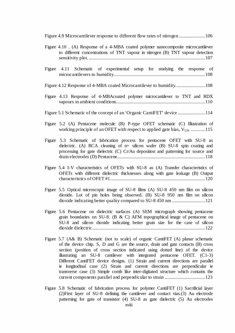
Figure 4.9 Microcantilever response to different flow rates of nitrogen ...................... 106
Figure 4.10 . (A) Response of a 4-MBA coated polymer nanocomposite microcantilever to different concentrations of TNT vapour in nitrogen (B) TNT vapour detection sensitivity plot. .................................................................................................. 107
Figure 4.11 Schematic of experimental setup for studying the response of microcantilevers to humidity............................................................................. 108
Figure 4.12 Response of 4-MBA coated Microcantilever to humidity......................... 108
Figure 4.13 Response of 4-MBAcoated polymer microcantilever to TNT and RDX vapours in ambient conditions........................................................................... 110
Figure 5.1 Schematic of the concept of an ‘Organic CantiFET’ device ....................... 114
Figure 5.2 (A) Pentacene molecule (B) P-type OFET schematic (C) Illustration of working principle of an OFET with respect to applied gate bias, VGS. ............ 115
Figure 5.3 Schematic of fabrication process for pentacene OFET with SU-8 as dielectric. (A) RCA cleaning of n+ silicon wafer (B) SU-8 spin coating and processing for gate dielectric (C) Cr/Au deposition and patterning for source and drain electrodes (D) Pentacene.......................................................................... 118
Figure 5.4 I-V characteristics of OFETs with SU-8 as (A) Transfer characteristics of OFETs with different dielectric thicknesses along with gate leakage (B) Output characteristics of OFET #1................................................................................ 120
Figure 5.5 Optical microscopic image of SU-8 films (A) SU-8 450 nm film on silicon dioxide. Lot of pin holes being observed. (B) SU-8 950 nm film on silicon dioxide indicating better quality compared to SU-8 450 nm ............................ 121
Figure 5.6 Pentacene on dielectric surfaces (A) SEM micrograph showing pentacene grain boundaries on SU-8. (B & C) AFM topographical image of pentacene on SU-8 and silicon dioxide indicating better grain size for the case of silicon dioxide dielectric ............................................................................................... 122
Figure 5.7 (A& B) Schematic (not to scale) of organic CantiFET (A) planar schematic of the device chip. S, D and G are the source, drain and gate contacts (B) cross section (position of cross section indicated using dotted line) of the device illustrating an SU-8 cantilever with integrated pentacene OFET. (C1-3) Different CantiFET device designs. (1) Strain and current directions are parallel ie longitudinal case (2) Strain and current directions are perpendicular ie transverse case (3) Simple comb like inter-digitated structure which contains the current components parallel and perpendicular to strain .................................. 123
Figure 5.8 Schematic of fabrication process for polymer CantiFET (1) Sacrificial layer (2)First layer of SU-8 defining the cantilever and contact vias.(3) Au electrode patterning for gate of transistor (4) SU-8 as gate dielectric (5) Au electrodes
xix
defining the source and drain of OFET (6) Thick SU-8 layer defined for anchor or chip of the cantiFET device. A photograph of the processed silicon wafer after this final lithography step is on right side (7) Release of the CantiFET device from substrate and pentacene deposition (8) final device structure showing cantilevers , source drain and gate contacts through vias ................... 125
Figure 5.9 (A) Photographs of released arrays of organic CantiFETs (B) SEM micrograph of the fabricated CantiFET device (C) Bottom and enlarged view of cantilever portion of the CantiFET from SEM showing the inter digitated source drain electrode configuration (Type 1 & 3 CantiFET) (D) Top and enlarged view of cantilever portion of the CantiFET from SEM ............................................. 128
Figure 5.10 I-V characteristics of organic CantiFETs after silicon nitride encapsulation. (A) Transfer characteristics indicating good ION/IOFF ratio (2.2 x 10³). Saturation field effect mobility and threshold voltage extracted from |IDS|1/2 vs. VGS characteristics as shown were 2.9 x 10⁻⁴ cm2/Vs and -11.5 V. (B) Output characteristics of silicon nitride encapsulated organic CantiFETs.................... 130
Figure 5.11 Load segment of beam bending experiment on organic CantiFET using nanoindenter ...................................................................................................... 130
Figure 5.12 Load displacement characteristics of Organic CantiFET. Inset showing the optical micrograph of the image indicating the location of indenter placement. ........................................................................................................................... 131
Figure 5.13 I-V characteristics of organic CantiFET obtained from electromechanical characterization. (A) Transfer characteristics of an organic CantiFET (CantiFET # 3) under different amount of bending. (B) IDS-VDS characteristics (@VDS = -40 V) under different amounts of bending ........................................................ 132
Figure 5.14 Percentage change in drain current, saturation field effect mobility and threshold voltage of the organic CantiFET # 3 as a function of percentage strain ........................................................................................................................... 134
Figure 5.15 Percentage change in drain of as a function of percentage strain (A) CantiFET # 1 The average value of Idsat at strain %= 0 was 11 nA (B) CantiFET # 2. The average value of Idsat at strain %= 0 was 6 nA .................................... 135
Figure 5.16 Mean and standard deviation of percentage change in drain current as a function of percentage strain for 5 cantiFET devices. ...................................... 136
Figure 5.17(A) Block diagram schematic of the setup used for measuring the 1/f noise. Device under test (DUT) is the cantiFET device. (B) 1/f like noise characteristics of Organic CantiFET. ................................................................ 137
Figure A1.1 (a) Case 1 considered in King’s analysis. The schematic of flat punch indenter indenting a film of thickness t. (b) Case 2 considered in modified King’s analysis. The schematic of Berkovich indenter indenting a film of thickness t to a depth of h [109]. ....................................................................... 145
xx
Figure A1.2 Plot of α as a function of normalized punch size [109]. ........................... 146
Figure A2.1 Schematic of polymer MEMS accelerometer (A) Planar schematic of SU-8 accelerometer with embedded SU-8/CB composite. (B) Cross sectional schematic of one of the legs of beams indicating individual layer thicknesses 148
Figure A2.2. Schematic of fabrication process for polymer composite MEMS accelerometer .................................................................................................... 149
Figure A2.3SEM micrographs of the fabricated SU-8 nanocomposite MEMS accelerometer .................................................................................................... 149
Figure A2.4Resonance frequency plot for polymer composite MEMS accelerometer 150
Figure A2.5 Microaccelerometer proof mass displacement vs. acceleration................ 150
Figure A2.6 Static electromechanical characterization of SU-8 nanocomposite beam connected in Wheatstone bridge. Refer Chapter 4 for measurement scheme. .. 151
List of tables
Table 1-1 Comparison of main classes of transduction schemes.................................... 17
Table 1-2 Applications of microcantilever-based sensors [77]....................................... 22
Table 1-3 Vapour pressures and molecular weights of some explosives [24] ................ 24
Table 2-1 SU-8 material properties ................................................................................. 36
Table 2-2 SU-8 microcantilever specifications ............................................................... 36
Table 2-3 Optimized process parameters for SU-8 microcantilevers ............................. 44
Table 3-1 Dimensional parameters of polymer nanocomposite microcantilever ........... 64
Table 3-2 Details of polymer nanocomposite thin film samples prepared for nanoindentation experiments............................................................................... 74
Table 3-3 Summary of performances of SU-8 /CB nanocomposite microcantilevers compared with other existing polymer microcantilever sensors ......................... 95
Table 5-1 Layer details of OFETs fabricated for performance evaluation of pentacene OFETs with SU-8 dielectric. ............................................................................. 119
Table 5-2 Specifications of OFETs with SU-8 as dielectric ......................................... 119
Table 5-3 Specifications of organic CantiFET device chips......................................... 128
Table 5-4 Comparison of performances of organic CantiFET and other nanomechanical cantilever sensors .............................................................................................. 138
Table 6-1Performance of the developed nanomechanical cantilever sensors compared to existing polymer nanomechanical cantilever sensors ....................................... 143
Table A3-1 Process details of different SU-8 layers in SU-8 nanocomposite microcantilevers ................................................................................................ 154
Table A3-2 Process details of different SU-8 layers in optimized SU-8 nanocomposite microcantilevers ................................................................................................ 155
Table A3-3 Process details of different SU-8 layers in Organic CantiFET .................. 156
xxii
Chapter 1
Introduction and Literature Review
1.1 Introduction to the topic
A sensor may be defined as a device that converts a nonelectrical, physical or chemical input
into an electrical output signal. According to Middlehoek, sensors can be classified according
to the energy domain of its primary input/output as electrical, thermal, radiation, mechanical,
magnetic and bio/chemical sensors [1]. The evolution of today’s microsensors with at least
one physical dimension at the sub-millimetre level happened due to the revolutions in the
field of microelectronics. The well-established integrated circuit industry played an
indispensable role in fostering an environment suitable for the development of microsystems
known as microelectromechanical systems (MEMS) [2]. MEMS sensors are used in various
industrial, consumer, defence and biomedical applications. Micro accelerometers, pressure
sensors and microarrays are some of the commercially available MEMS sensors. MEMS
being a technology derived from microelectronics, these miniature MEMS sensors hold
advantages such as, low cost of production due to very large production volume and fewer
materials, easy integration with required instrumentation on microelectronics chips, arraying
capability enabling multiplexed measurements, greater portability, robustness and low power
consumption. Many tools used in the design and manufacturing of MEMS devices are
borrowed from the conventional IC industry. Hence silicon is considered to be the primary
2
material even in MEMS though MEMS systems using other materials like polymers, metals
and ceramics have been demonstrated.
There have always been demands for the detection of very low levels of a large number of
chemical and biological substances in application areas such as environmental monitoring,
healthcare, biomedical technology, clinical analysis and food processing. For example in the
case of homeland security applications, recent increase in security concerns in public places
like airports and public transports have increased the demand for low-cost portable, efficient,
and easy to use explosive sensing technology. The emergence of MEMS and nanotechnology
along with these demands enabled the development of a class of microsensor systems called
as microfabricated bio/chemical sensors. Bio/chemical sensors combine a bio/chemical
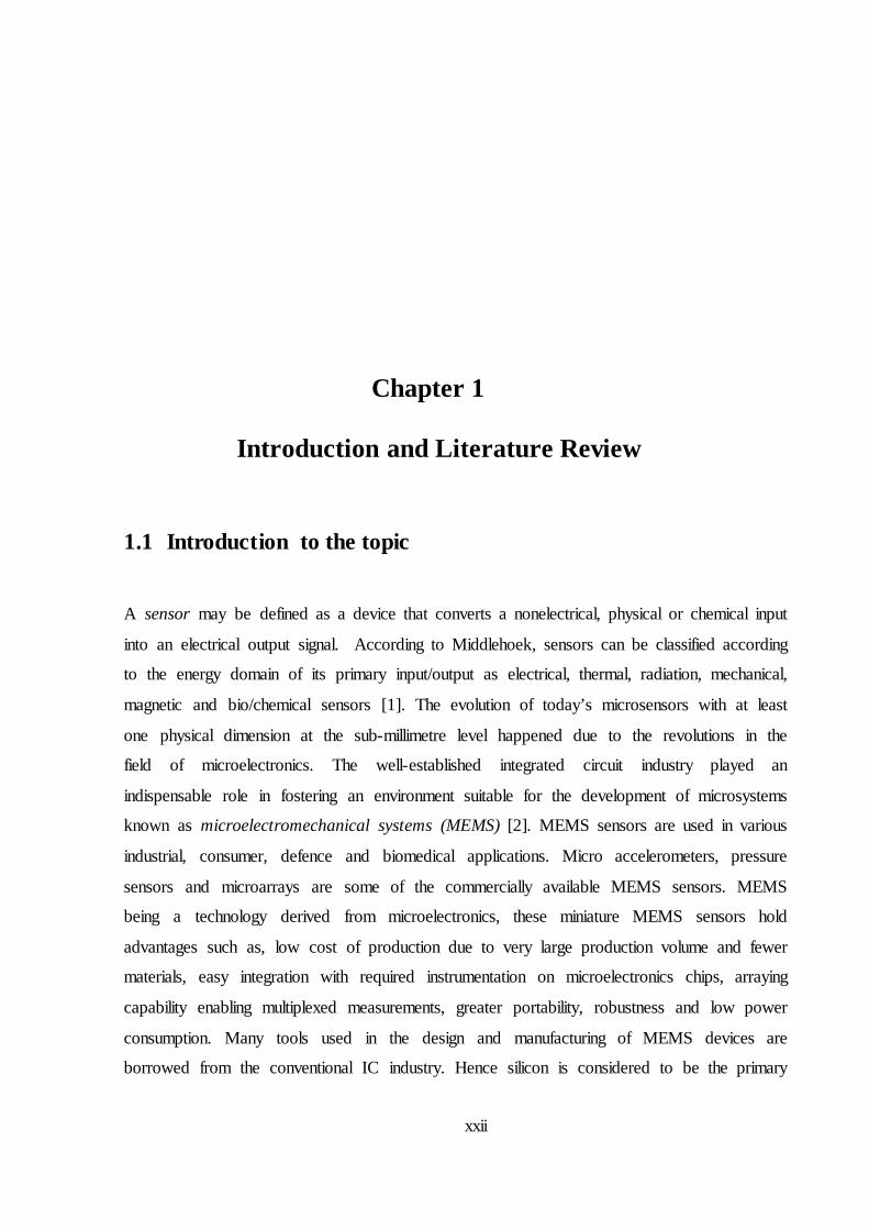
recognition element coupled to a physical transducer [3]. A biological or chemical
recognition element recognizes a specific target analyte and does not recognize other analytes,
which imparts selectivity to the sensor (Figure 1.1). The transducer translates the
bio/chemical-recognition event into measurable quantities such as change in electrical signal,
an optical emission, a mechanical motion etc. In the case of biosensors, the recognition
element may be an enzyme, antibody, antigen, living cells, tissues, etc. and in the case of
chemical sensors, these can be any chemical substance specific for the target analyte.
Figure 1.1 Schematic representation of selectivity in bio/chemical sensors
A class of MEMS sensors known as microcantilever sensors (nanomechanical cantilever
sensors) came into existence as atomic force microscopy (AFM) probes [4] and they have a
huge potential as platforms for the development of many physical [5], chemical [6], and
biological sensors [7-9].
3
1.2 Motivation
Development of bio/chemical sensing application using microcantilevers for a wide variety of
applications opens challenging and interesting research problems as these have a definite edge
over other sensors owing to its versatility, sensitivity, scope for miniaturization and
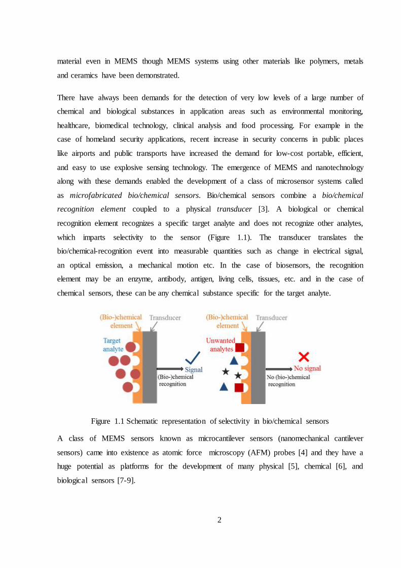
parallelization and low cost. Microcantilever based bio/chemical sensors work on the
principle of conversion of the bio/chemical recognition event into nanomechanical motion
[10]. The cause for nanomechanical motion can be due the free energy change on the surface
of the sensor due to the reaction of the target analyte with the receptor molecule or due to the
mass change on addition of the target analyte bound to the microcantilever surface (Figure
1.2).
Figure 1.2 Principle of microcantilever based bio/chemical sensor
These nanomechanical cantilever sensors offer many orders of magnitude higher sensitivity in
comparison to other commonly used bio/chemical sensors such as quartz crystal
microbalances (QCM), flexural plate wave oscillators (FPW), and surface acoustic wave
devices (SAW) [11]. The distinct advantages of the nanomechanical cantilever sensors that
support their candidature for bio/chemical sensing applications can be enlisted as given
below:-
Smaller size with surface area of the order of 10-5 cm2, orders of magnitude smaller
compared to the QCM and SAW devices [11].
Miniaturization and mass production at a relatively low cost using standard
semiconductor manufacturing processes.
4
Several modes of operation (static mode used for measuring surface stress change,
resonant mode used for detecting mass loading, heat mode etc.) in comparison to
single mode of operation (gravimetric) for other sensors.
Large surface to volume ratio: - Hence the change in the Gibbs surface free energy
induced by surface-analyte interactions lead to large surface forces. Mass loading also
leads to larger amplitude of displacement or larger changes in resonant frequencies in
comparison to other sensors. Microcantilevers possess superior sensitivities for
detection of many chemical and biological analytes. This high sensitivity is attributed
to large surface to volume ratio and ability to detect cantilever motion with sub-
nanometre precision
Bio/chemical selectivity: - Selectivity can be imparted to microcantilever sensors
using biological or chemically selective layers like in the cases of SAW and QCM
based sensors.
Improved dynamic response.
Label free detection, an important characteristics in the case of biosensors.
Increased reliability and precision compared to other conventional sensors.
Feasibility for fabrication of multi-element sensors arrays supporting high degree of
parallelization
Ease of integration of microcantilever sensor with on-chip electronic circuitry.
Considering the demand for development of ultra-sensitive, versatile and cost effective sensor
platforms along with the above mentioned advantages of microcantilever sensors, a detailed
literature survey has been carried out in different aspects of research in microcantilever based
bio/chemical sensors. Objectives and scope of this thesis were formulated based on the
literature review being presented in the next section.

5
1.3 Microcantilevers as bio/chemical sensors-Literature review
Different research aspects in the development of microcantilevers based bio/chemical sensors
are covered in this literature survey. The key aspects include the different sensing modes of
operation of microcantilevers, various structural materials for microcantilevers, transduction
schemes that are used to measure and convert the changes in mechanical parameters of the
microcantilevers to useful signals and an overview of different applications of
microcantilevers in the field of bio/chemical sensing. Advancements in one of the chemical
sensing applications, i.e., microcantilever for sensing explosive vapours is covered as a
separate subsection, as this is known to be a challenging and an important application and is
also one of the on-going research topics of interest in this field.
1.3.1 Sensing modes and principles
The sensing operation modes of microcantilevers could be broadly classified based on their
principles in translating the recognition event into nanomechanical motion. Typically there
are three modes of operation such as static mode, dynamic mode and heat mode [12] . In static
mode, the bending of the microcantilever upon the molecular adsorption is measured. In
dynamic mode, the dependence of resonant frequency of the microcantilever on the mass of
the microcantilever is exploited. The heat mode, takes advantage of the bimetallic or bimorph
effect that leads to a bending of a biomaterial microcantilever with change in temperature.
Figure 1.3 pictorially depicts these modes of operation in different scenarios. It would be
appropriate to discuss the details of these modes of operation [12].
(1) Static mode
The static deflection of a microcantilever is related to the difference in surface stress of the
two faces of microcantilever. When one of the surfaces of the microcantilever is
functionalized with a receptor layer, the adsorption or binding of target molecule or material
to the receptor layer leads to a differential surface stress between top and bottom of the
microcantilever. Uniform compressive or tensile stress acting on an isotropic material tends to
increase or decrease the surface area.
6
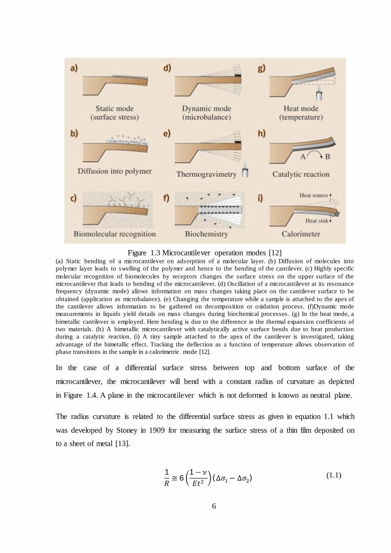
Figure 1.3 Microcantilever operation modes [12]
(a) Static bending of a microcantilever on adsorption of a molecular layer. (b) Diffusion of molecules into polymer layer leads to swelling of the polymer and hence to the bending of the cantilever. (c) Highly specific molecular recognition of biomolecules by receptors changes the surface stress on the upper surface of the microcantilever that leads to bending of the microcantilever. (d) Oscillation of a microcantilever at its resonance frequency (dynamic mode) allows information on mass changes taking place on the cantilever surface to be obtained (application as microbalance). (e) Changing the temperature while a sample is attached to the apex of the cantilever allows information to be gathered on decomposition or oxidation process. (f)Dynamic mode measurements in liquids yield details on mass changes during biochemical processes . (g) In the heat mode, a bimetallic cantilever is employed. Here bending is due to the difference in the thermal expansion coefficients of two materials. (h) A bimetallic microcantilever with catalytically active surface bends due to heat production during a catalytic reaction. (i) A tiny sample attached to the apex of the cantilever is investigated, taking advantage of the bimetallic effect. Tracking the deflection as a function of temperature allows observation of phase transitions in the sample in a calorimetric mode [12].
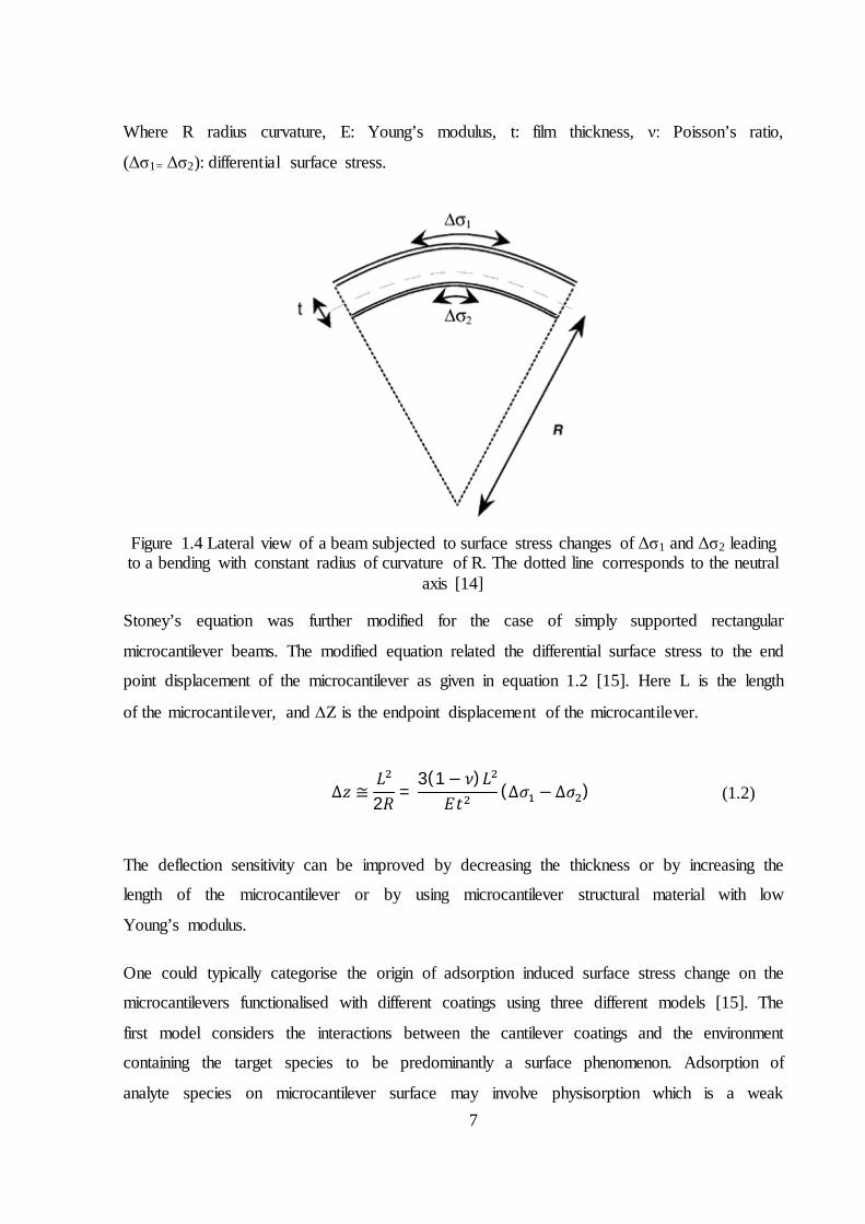
In the case of a differential surface stress between top and bottom surface of the
microcantilever, the microcantilever will bend with a constant radius of curvature as depicted
in Figure 1.4. A plane in the microcantilever which is not deformed is known as neutral plane.
The radius curvature is related to the differential surface stress as given in equation 1.1 which
was developed by Stoney in 1909 for measuring the surface stress of a thin film deposited on
to a sheet of metal [13].
1푅≅ 6
1− 휈퐸푡
(Δ휎 − Δ휎 ) (1.1)
7
Where R radius curvature, E: Young’s modulus, t: film thickness, ν: Poisson’s ratio,
(Δσ1= Δσ2): differential surface stress.
Figure 1.4 Lateral view of a beam subjected to surface stress changes of Δσ1 and Δσ2 leading to a bending with constant radius of curvature of R. The dotted line corresponds to the neutral
axis [14]
Stoney’s equation was further modified for the case of simply supported rectangular
microcantilever beams. The modified equation related the differential surface stress to the end
point displacement of the microcantilever as given in equation 1.2 [15]. Here L is the length
of the microcantilever, and Z is the endpoint displacement of the microcantilever.
∆푧 ≅
퐿2푅
=3(1− 휈)퐿
퐸푡(Δ휎 − Δ휎 ) (1.2)
The deflection sensitivity can be improved by decreasing the thickness or by increasing the
length of the microcantilever or by using microcantilever structural material with low
Young’s modulus.
One could typically categorise the origin of adsorption induced surface stress change on the
microcantilevers functionalised with different coatings using three different models [15]. The
first model considers the interactions between the cantilever coatings and the environment
containing the target species to be predominantly a surface phenomenon. Adsorption of
analyte species on microcantilever surface may involve physisorption which is a weak
8
bonding with binding energy less than 0.1 eV or chemisorption which is a stronger bonding
with typical binding energy more than 0.3 eV [15]. The surface stress changes typically can
be attributed to the Gibbs free energy changes associated with the adsorption process. An
example of a chemisorption process of thiol molecules on gold coated microcantilever leading
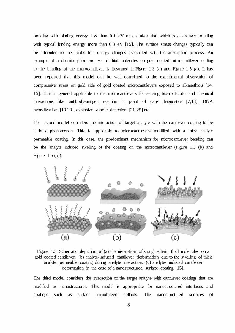
to the bending of the microcantilever is illustrated in Figure 1.3 (a) and Figure 1.5 (a). It has
been reported that this model can be well correlated to the experimental observation of
compressive stress on gold side of gold coated microcantilevers exposed to alkanethiols [14,
15]. It is in general applicable to the microcantilevers for sensing bio-molecular and chemical
interactions like antibody-antigen reaction in point of care diagnostics [7,18], DNA
hybridization [19,20], explosive vapour detection [21-25] etc.
The second model considers the interaction of target analyte with the cantilever coating to be
a bulk phenomenon. This is applicable to microcantilevers modified with a thick analyte
permeable coating. In this case, the predominant mechanism for microcantilever bending can
be the analyte induced swelling of the coating on the microcantilever (Figure 1.3 (b) and
Figure 1.5 (b)).
Figure 1.5 Schematic depiction of (a) chemisorption of straight-chain thiol molecules on a
gold coated cantilever. (b) analyte-induced cantilever deformation due to the swelling of thick analyte permeable coating during analyte interaction. (c) analyte- induced cantilever
deformation in the case of a nanostructured surface coating [15].
The third model considers the interaction of the target analyte with cantilever coatings that are
modified as nanostructures. This model is appropriate for nanostructured interfaces and
coatings such as surface immobilized colloids. The nanostructured surfaces of

9
microcantilevers facilitate an efficient conversion of the energy of target-receptor interactions
which is a combination of bulk, surface, and inter-surface interactions to mechanical energy.
Nanostructured coatings substantially increase the number of binding sites per cantilever
surface and hence sensitivity of the sensor.
(2) Dynamic mode
The resonance frequency, f of an oscillating microcantilever can be expressed as equation 1.3.
The equation is used for first mode of vibration.
푓 =
12휋
퐾푚∗ (1.3)
where K is the spring constant and m* is the effective mass of the microcantilever [26].
Resonance frequency may change due to changes in mass or changes in spring constant and
the change in frequency can be expressed as equation 1.4 [26].
푑푓(푚∗ ,퐾) =
휕푓휕푚∗ 푑푚∗ +
휕푓휕퐾
푑퐾 = 푓2푑퐾퐾
−푑푚∗
푚∗ (1.4)
The contribution from spring constant (dK/K term) can be minimized by using appropriate
designs for microcantilevers with localized adsorption areas at the terminal end of the
cantilever (Figure 1.3(d)). Hence variation in resonance frequency is direct indication of mass
loading as expressed in equation 1.5.
∆푚 =
퐾4휋
1푓
−1푓
(1.5)
where f0 and f1 are microcantilever resonance frequencies before and after molecular
adsorption. The sensitivity and hence the minimum detectable mass depends on the ratio of
the mass and the resonant frequency of the microcantilever. Thus the sensitivity can be
enhanced by decreasing the dimensions of the microcantilever. By coupling the mass change
10
with varying environment temperature conditions, resonant mode of operation could be
extended to micromechanical thermogravimetry applications (Figure 1.3(e)).
The resolution of mass sensing of microcantilevers operating in dynamic mode in liquid
medium is expected to get affected due to damping effects. Hence dynamic mode of
microcantilevers might not be appropriate for sensing applications with liquid medium that
would demand very high resolution.
(3) Heat mode
Microcantilevers made of two material layers with different thermal expansion coefficients
undergo thermally induced stress and deformation. Microcantilever bending could be due to
external temperature changes (Figure 1.3 (g)) due to the heat generated on the microcantilever
surface either by exothermal reactions (Figure 1.3 (h)) or due to the heat associated with the
analyte adsorption (micromechanical calorimetry Figure 1.3 (i)). The last two cases are
directly related to cantilever based calorimetry for bio/ chemical sensors.
1.3.2 Microcantilever materials
Most commonly used microcantilever structural materials are single crystalline silicon,
polycrystalline silicon, silicon nitride, silicon dioxide and mechanically stable polymers like
SU-8, TOPAS and Parylene [27-29].
There has always been a demand for bio/chemical sensors with very high sensitivity so as to
detect bio-molecular interactions in the case of medical diagnostics or to sniff very small
amount of hazardous gases or explosive vapours for security applications.
As per the working principle of microcantilever based surface stress sensor, the sensitivity is
determined by the stiffness of the cantilever structure (dictated by the Young's modulus of the
material). Though the commercial cantilevers are made out of silicon derived materials that
have a higher Young's modulus, the need for highly sensitive and inexpensively fabricated
microcantilever sensors lead to a diversion from conventional silicon micromachining
technologies towards polymer based microcantilever technologies. Among the polymers
reported for microfabrication, SU-8 which is an epoxy based polymer developed by IBM, is
the most commonly used polymer structural material in MEMS [30-32]. Since 1999 [33], the
11
use of SU-8 polymer which is considered as a high aspect ratio negative photoresist for
MEMS applications has been exponentially growing during the last couple of years [34-
36][35]. Due to its ability in forming patterns with wide range of thickness varying from few
hundred of nanometres to a few millimetres with high aspect ratios, SU-8 has been a popular
and cost effective alternative to silicon for the fabrication of micro scale components such as
micro channels, micro-moulds for electroplating or masters for hot embossing.
Considering its applicability as a structural material for microcantilevers, SU-8 seems to be a
good candidate with its inherent advantages such as
Lower Young's modulus (Expected improvement in sensitivity)
Inexpensive and less complex fabrication process.
SU-8 is a well understood UV and e-beam resist
Fabrication processes consume lesser amount of chemicals and gases and low
temperature processing making it cost effective.
Mechanical and thermal stability
Compatibility for integrating sensor with microfluidics (important for biosensor
applications)
1.3.3 Transduction principles
The performance of a microcantilever sensor relies on real-time measurements and the
resolution of measurements of cantilever mechanical parameters during sensing operation.
These parameters include microcantilever tip displacement, spatial orientation, radius of
curvature, and intrinsic stress. Transduction schemes can be chosen based on mode of
operation i.e., static or dynamic; microcantilever design, microcantilever material and the
magnitude of expected response from the microcantilever. Microcantilever transduction
schemes can be broadly classified as optical and electrical. There are a variety of electrical
transduction schemes such as piezoresistive, piezoelectric, capacitive, electron tunnelling
technique and embedded MOSFET technique. The principles of operation of some of the
12
selected techniques are briefly presented here. The inherent advantages and disadvantages of
each transduction scheme are provided as Table 1-1.
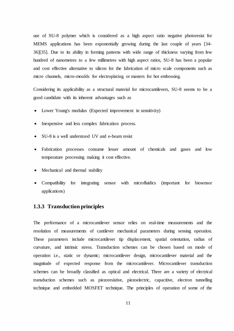
(1) Optical lever method
Optical read-out is one of the most common and simplest schemes for detecting the
movement of microcantilevers and is derived from the standard AFM arrangement. In optical
lever method, the laser is focused at the free end of the microcantilever and the reflected laser
beam is detected using a position-sensitive photo detector (PSD) and the measurement can be
correlated to get the displacement information as shown in Figure 1.6 (A).
This method is expected to provide sub-angstrom resolution and can be implemented easily.
Referring to Table 1-1, implementation of this technique for readout of microcantilever arrays
is technologically challenging as (i) it requires an array of laser sources with the same number
of elements as that of the microcantilever array, and with the same pitch distance. (ii)
Sequential switching (on and off) of each laser source is also necessary to avoid overlapping
of the reflected beams on the photo-detector. Another optical transduction scheme developed
by IBM [8,37,38], allows the measurement of deflection of eight microcantilevers using an
array of vertical cavity surface emitting lasers (VCSELs). The same pitch has to be
maintained in both microcantilever and VCSEL arrays. A single photo-detector tracks the
movement of the spots reflected from respective cantilever.
Figure 1.6 Schematic of (A)"optical lever" readout that is commonly used to measure the
deflection of microcantilever probes in standard AFM [8] (B) interferometric readout [39]
Another optical approach using CCD camera in place of PSD has been developed by a
research group in University of California, Berkeley, USA. In this method, a two dimensional
array of microcantilevers is illuminated simultaneously resulting in a two-dimensional array
of reflected laser spots that are captured by a high resolution CCD camera. Such an approach
13
has been demonstrated to be used in microcantilever array based bio/chemical sensors for
multiple analyte detections [39, 40].
(2) Interferometric transduction
This method is based on the interference that occurs between a reference laser beam and the
reflected beam from the microcantilever [39]. Differential measurement between two
microcantilevers is preferred over single microcantilever measurements for eliminating the
environmental disturbances. A schematic of an interferometric sensor that inherently
measures the differential bending between two adjacent microcantilevers is shown in Figure
1.6(B). The cantilevers are supported by L-shaped structures, with interdigitated fingers
between the supports and the microcantilevers to form diffraction gratings. This allows
measurements of absolute deflection of each individual microcantilever. The interdigitated
fingers between the two microcantilevers enable differential measurement.
(3) Piezoresistive
Piezoresistive read out is based on the surface stress induced changes observed in the
resistivity of a piezoresistive material layer embedded inside the cantilever [42].
Piezoresistivity is a material property where the bulk resistivity of a material changes with
strain. The ratio of the relative change in resistance per unit strain is called gauge factor, K
which is the product of piezoresistive coefficient and Young’s modulus of the material. The
relation between the strain, ε and the relative change in resistance for a piezoresistor is given
by equation 1.6.
∆푅푅
= 퐾휀 (1.6)
∆푅푅
= (1 + 2휈)휀 +Δ휌휌
(1.7)
Here R : resistance, ν :Poisson’s ratio, ε: strain, ρ : resistivity of the piezoresistor. The change
in resistance might be due to both geometric effects (1+ 2ν) and the fractional change in
resistivity (Δρ/ρ) of the material with strain and hence can be represented as equation 1.7 [43].
14
The gauge factor contribution from geometric effects alone could be approximately in the
range of 1.4-2.0. In the case of metals, the Δρ/ρ term is very negligible. However, in the case
of semiconductor materials such as silicon, the Δρ/ρ can be 50–100 times larger than the
geometric term [43].
Consider a single layer microcantilever of thickness h with an infinitely thin piezoresistor on
top (Figure 1.7). In the case of surface stress induced on top of the cantilever, the surface
stress sensitivity can be expressed as equation 1.8 [34]. The assumption made is that, the
piezo-layer thickness tends to zero and neutral axis is placed at the middle of the
microcantilever structure.
∆푅푅
= 4퐾퐸ℎ
휎 (1.8)
Here, E: Young’s modulus of the structural material, h: the thickness of the microcantilever,
K: gauge factor of the thin piezoresistor and휎 : surface stress. This equation implies that for a
given thickness h of a microcantilever, the surface stress sensitivity depends on the ratio K/E
which is the ratio of gauge factor of the piezoresistor and the Young's modulus of the
structural material. Since the strain is distributed in such a way that it changes its direction at
the neutral axis with zero strain along the neutral axis plane, in order to get good sensitivity, it
is advisable to keep the piezoresistor away from the neutral axis.
The most common electrical circuit configuration for measuring the change in resistance with
a provision for temperature compensation is a Wheatstone bridge circuit and the schematic of
the configuration with a piezoresistive microcantilever placed in one of the legs of the bridge
is as shown in Figure 1.7 (B). The output signal Vout is given by equation 1.9. Here, 푉 is the
bridge bias.
푉 =
14∆푅푅푉 (1.9)
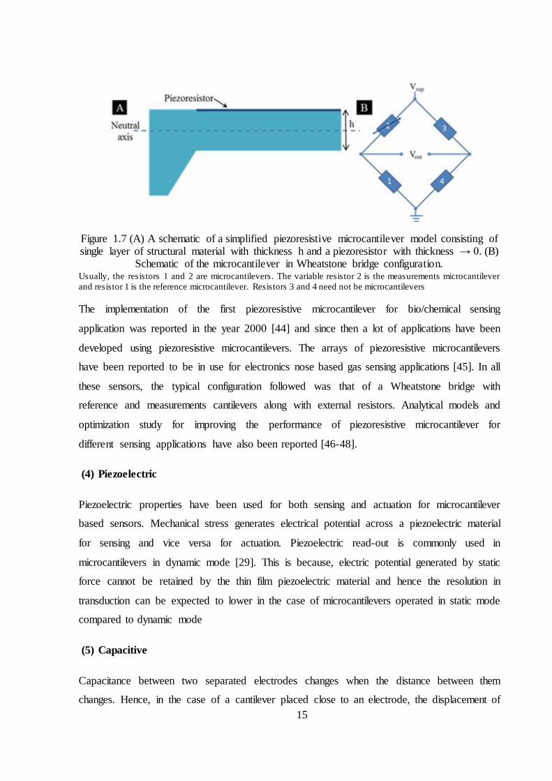
15
Figure 1.7 (A) A schematic of a simplified piezoresistive microcantilever model consisting of single layer of structural material with thickness h and a piezoresistor with thickness → 0. (B)
Schematic of the microcantilever in Wheatstone bridge configuration. Usually, the resistors 1 and 2 are microcantilevers. The variable resistor 2 is the measurements microcantilever and resistor 1 is the reference microcantilever. Resistors 3 and 4 need not be microcantilevers
The implementation of the first piezoresistive microcantilever for bio/chemical sensing
application was reported in the year 2000 [44] and since then a lot of applications have been
developed using piezoresistive microcantilevers. The arrays of piezoresistive microcantilevers
have been reported to be in use for electronics nose based gas sensing applications [45]. In all
these sensors, the typical configuration followed was that of a Wheatstone bridge with
reference and measurements cantilevers along with external resistors. Analytical models and
optimization study for improving the performance of piezoresistive microcantilever for
different sensing applications have also been reported [46-48].
(4) Piezoelectric
Piezoelectric properties have been used for both sensing and actuation for microcantilever
based sensors. Mechanical stress generates electrical potential across a piezoelectric material
for sensing and vice versa for actuation. Piezoelectric read-out is commonly used in
microcantilevers in dynamic mode [29]. This is because, electric potential generated by static
force cannot be retained by the thin film piezoelectric material and hence the resolution in
transduction can be expected to lower in the case of microcantilevers operated in static mode
compared to dynamic mode
(5) Capacitive
Capacitance between two separated electrodes changes when the distance between them
changes. Hence, in the case of a cantilever placed close to an electrode, the displacement of
16
the cantilever would cause a change in capacitance of this parallel plate arrangement. This
electric read-out was initially introduced in the case of AFM probes [49] and was
subsequently implemented for microcantilever based sensors. This readout is known to be
sensitive to changes in refractive index of the medium and is not suitable for liquid media.
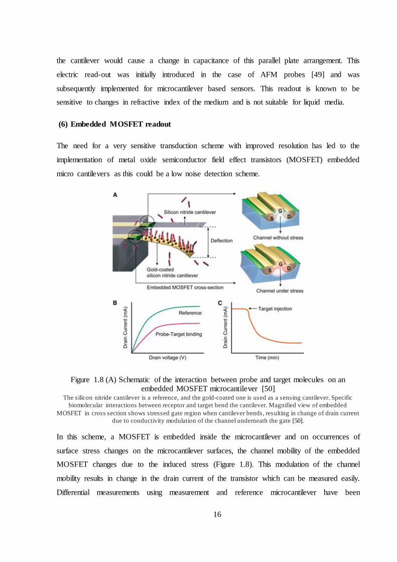
(6) Embedded MOSFET readout
The need for a very sensitive transduction scheme with improved resolution has led to the
implementation of metal oxide semiconductor field effect transistors (MOSFET) embedded
micro cantilevers as this could be a low noise detection scheme.
Figure 1.8 (A) Schematic of the interaction between probe and target molecules on an embedded MOSFET microcantilever [50]
The silicon nitride cantilever is a reference, and the gold-coated one is used as a sensing cantilever. Specific biomolecular interactions between receptor and target bend the cantilever. Magnified view of embedded
MOSFET in cross section shows stressed gate region when cantilever bends, resulting in change of drain current due to conductivity modulation of the channel underneath the gate [50].
In this scheme, a MOSFET is embedded inside the microcantilever and on occurrences of
surface stress changes on the microcantilever surfaces, the channel mobility of the embedded
MOSFET changes due to the induced stress (Figure 1.8). This modulation of the channel
mobility results in change in the drain current of the transistor which can be measured easily.
Differential measurements using measurement and reference microcantilever have been
17
reported. The performance of the microcantilevers using this scheme has been reported to be
better compared to those of piezoresistive scheme in terms of sensitivity and noise [50].
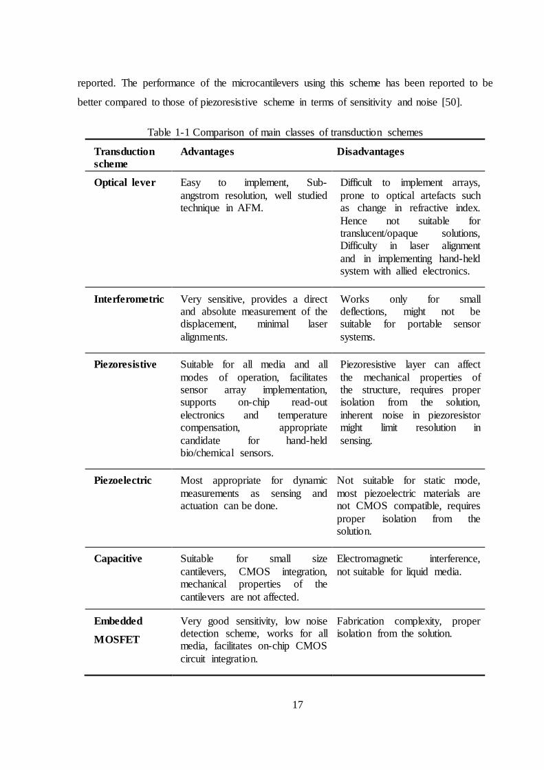
Table 1-1 Comparison of main classes of transduction schemes
Transduction scheme
Advantages Disadvantages
Optical lever Easy to implement, Sub-angstrom resolution, well studied technique in AFM.
Difficult to implement arrays, prone to optical artefacts such as change in refractive index. Hence not suitable for translucent/opaque solutions, Difficulty in laser alignment and in implementing hand-held system with allied electronics.
Interferometric Very sensitive, provides a direct and absolute measurement of the displacement, minimal laser alignments.
Works only for small deflections, might not be suitable for portable sensor systems.
Piezoresistive Suitable for all media and all modes of operation, facilitates sensor array implementation, supports on-chip read-out electronics and temperature compensation, appropriate candidate for hand-held bio/chemical sensors.
Piezoresistive layer can affect the mechanical properties of the structure, requires proper isolation from the solution, inherent noise in piezoresistor might limit resolution in sensing.
Piezoelectric Most appropriate for dynamic measurements as sensing and actuation can be done.
Not suitable for static mode, most piezoelectric materials are not CMOS compatible, requires proper isolation from the solution.
Capacitive Suitable for small size cantilevers, CMOS integration, mechanical properties of the cantilevers are not affected.
Electromagnetic interference, not suitable for liquid media.
Embedded
MOSFET
Very good sensitivity, low noise detection scheme, works for all media, facilitates on-chip CMOS circuit integration.
Fabrication complexity, proper isolation from the solution.
18
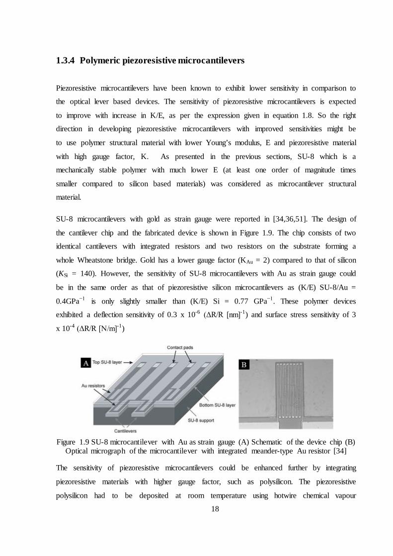
1.3.4 Polymeric piezoresistive microcantilevers
Piezoresistive microcantilevers have been known to exhibit lower sensitivity in comparison to
the optical lever based devices. The sensitivity of piezoresistive microcantilevers is expected
to improve with increase in K/E, as per the expression given in equation 1.8. So the right
direction in developing piezoresistive microcantilevers with improved sensitivities might be
to use polymer structural material with lower Young’s modulus, E and piezoresistive material
with high gauge factor, K. As presented in the previous sections, SU-8 which is a
mechanically stable polymer with much lower E (at least one order of magnitude times
smaller compared to silicon based materials) was considered as microcantilever structural
material.
SU-8 microcantilevers with gold as strain gauge were reported in [34,36,51]. The design of
the cantilever chip and the fabricated device is shown in Figure 1.9. The chip consists of two
identical cantilevers with integrated resistors and two resistors on the substrate forming a
whole Wheatstone bridge. Gold has a lower gauge factor (KAu = 2) compared to that of silicon
(KSi = 140). However, the sensitivity of SU-8 microcantilevers with Au as strain gauge could
be in the same order as that of piezoresistive silicon microcantilevers as (K/E) SU-8/Au =
0.4GPa−1 is only slightly smaller than (K/E) Si = 0.77 GPa−1. These polymer devices
exhibited a deflection sensitivity of 0.3 x 10⁻⁶ (ΔR/R [nm]-1) and surface stress sensitivity of 3
x 10-4 (ΔR/R [N/m]-1)
Figure 1.9 SU-8 microcantilever with Au as strain gauge (A) Schematic of the device chip (B)
Optical micrograph of the microcantilever with integrated meander-type Au resistor [34]
The sensitivity of piezoresistive microcantilevers could be enhanced further by integrating
piezoresistive materials with higher gauge factor, such as polysilicon. The piezoresistive
polysilicon had to be deposited at room temperature using hotwire chemical vapour

19
deposition technique (HWCVD) [52,53]. However as polysilicon is a stiffer material than SU-
8, the film should be thin enough such that it does not add to the stiffness of the structure
while ensuring that the thin polysilicon does not lead to increased noise in measurements.
Piezoresistive materials with good gauge factor like that of polysilicon and modulus similar to
that of SU-8 would be the right choice. So the main goal of improvement in sensitivity
without compromising on the process complexity and thereby ensuring cost effectiveness can
only be accomplished by a proper choice of piezoresistive thin films containing similar
mechanical characteristics and process compatibility as that of SU-8. Composites of polymers
and conducting fillers such as carbon black (CB) and carbon nanotubes are known to exhibit
piezoresistive behaviour as reported in[54,55]. The suspension of different conducting
nanoparticles in SU-8 was reported in [56]. Hence polymer composites based on SU-8 with
conductive fillers could be a viable option for the embedded piezoresistive material in SU-8
microcantilevers. In such a device, the strain in the microcantilever is measured by the change
in resistance of the embedded piezoresistive layer containing conducting nanoparticles. When
the microcantilever structure is deformed or strained during a sensing operation, the
nanocomposite layer responds to the strain by increasing the distance (in the case of tensile
strain) between the individual conductive fillers. This eventually disturbs the conducting
network and leads to an increase in resistivity of the composite layer. A research work in this
direction was reported where piezoresistive polymer conductive filler composite made of SU-
8 and carbon black was integrated inside an SU-8 microcantilever [57].
Figure 1.10 Optical image of a micromachined SU-8 cantilever with integrated SU-8/carbon piezoresistor (Length = 200 m, Width = 200 m and thickness = 7 m) [57]
SU-8/CB nanocomposite piezoresistor patterned on an SU-8 layer for the microcantilever
structure is given in Figure 1.10 (B). Gamelgard et.al. [57], used piezoresistors that were
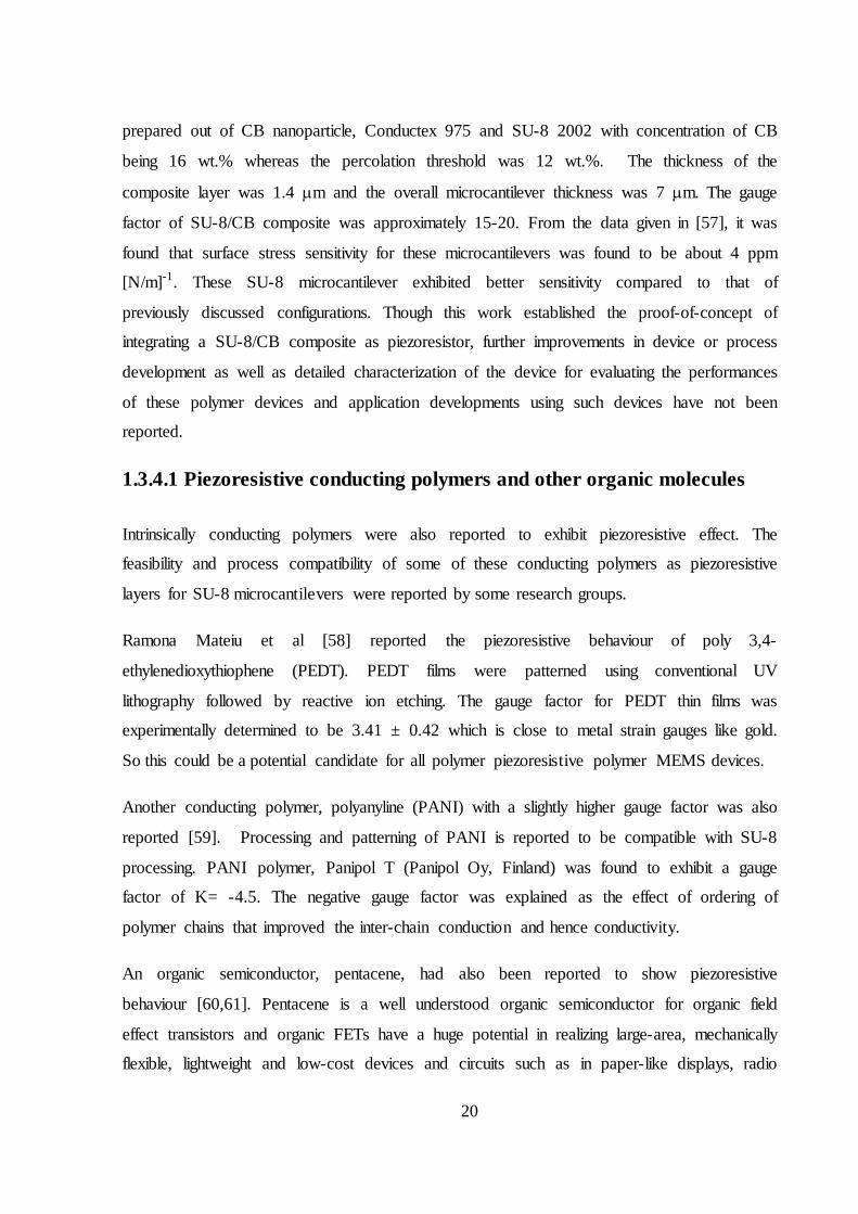
20
prepared out of CB nanoparticle, Conductex 975 and SU-8 2002 with concentration of CB
being 16 wt.% whereas the percolation threshold was 12 wt.%. The thickness of the
composite layer was 1.4 m and the overall microcantilever thickness was 7 m. The gauge
factor of SU-8/CB composite was approximately 15-20. From the data given in [57], it was
found that surface stress sensitivity for these microcantilevers was found to be about 4 ppm
[N/m]-1. These SU-8 microcantilever exhibited better sensitivity compared to that of
previously discussed configurations. Though this work established the proof-of-concept of
integrating a SU-8/CB composite as piezoresistor, further improvements in device or process
development as well as detailed characterization of the device for evaluating the performances
of these polymer devices and application developments using such devices have not been
reported.
1.3.4.1 Piezoresistive conducting polymers and other organic molecules
Intrinsically conducting polymers were also reported to exhibit piezoresistive effect. The
feasibility and process compatibility of some of these conducting polymers as piezoresistive
layers for SU-8 microcantilevers were reported by some research groups.
Ramona Mateiu et al [58] reported the piezoresistive behaviour of poly 3,4-
ethylenedioxythiophene (PEDT). PEDT films were patterned using conventional UV
lithography followed by reactive ion etching. The gauge factor for PEDT thin films was
experimentally determined to be 3.41 ± 0.42 which is close to metal strain gauges like gold.
So this could be a potential candidate for all polymer piezoresistive polymer MEMS devices.
Another conducting polymer, polyanyline (PANI) with a slightly higher gauge factor was also
reported [59]. Processing and patterning of PANI is reported to be compatible with SU-8
processing. PANI polymer, Panipol T (Panipol Oy, Finland) was found to exhibit a gauge
factor of K= -4.5. The negative gauge factor was explained as the effect of ordering of
polymer chains that improved the inter-chain conduction and hence conductivity.
An organic semiconductor, pentacene, had also been reported to show piezoresistive
behaviour [60,61]. Pentacene is a well understood organic semiconductor for organic field
effect transistors and organic FETs have a huge potential in realizing large-area, mechanically
flexible, lightweight and low-cost devices and circuits such as in paper-like displays, radio
21
frequency identification tags, and large area sensors on flexible substrates. However, the
effect of strain on the electrical behaviour of pentacene based OFETs has always been a
concern while discussing the reliability of OFETs for flexible electronics applications and
different device design ideas to overcome this effect is an on-going research for realizing
ultra-flexible OFET devices and circuits [62-64]. There are a very few reports available in
literature that investigated the effect of bending induced strain on change in current of
pentacene OFETs [61,65][66]. This negative aspect of dependence of electrical behaviour on
bending induced strain in pentacene OFETs for flexible electronics can be utilized in a
positive way in realizing sensor applications using pentacene. The reported applications of
pentacene as strain sensor include flexible strain sensors[60], large area force sensors[67],
tactile sensors and pressure sensors [68,69] all of them being large area sensors. The most
common deposition process for Pentacene is vacuum sublimation. This allows uniform
deposition of pentacene layers and the deposition process is done at room temperature making
it suitable for polymer substrates [70] . As pentacene is a well understood organic
semiconductor for organic field effect transistors, most of these reported sensor applications
employed pentacene based OFETs as strain sensor. This was highly beneficial as the
resistivity of pentacene thin films were known be very high (~2x10³ Ωm [71] and the
transistor configuration would support the arrays of sensors with built-in switching matrix
using these integrated OFETs.
1.3.5 Applications of microcantilever as bio/chemical sensors
Microcantilevers have been employed for various bio/chemical sensing applications that
could be categorized as (1) sensors in medicine and biology and (2) sensors in chemistry and
environmental monitoring. The most common microcantilevers based bio/chemical
applications demonstrated so far in literature can be listed as Table 1-2. In addition to these
categories, microcantilever based sensors can also be categorized as gas sensors and
biosensors.
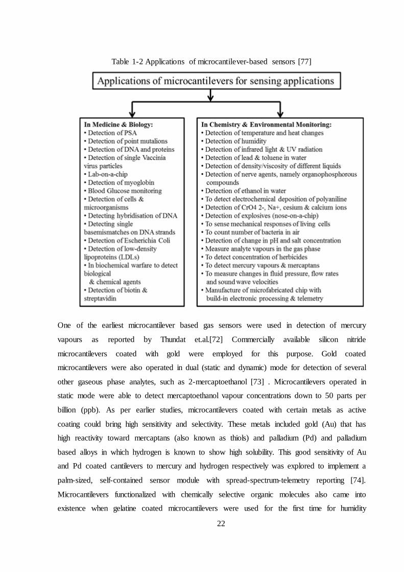
22
Table 1-2 Applications of microcantilever-based sensors [77]
One of the earliest microcantilever based gas sensors were used in detection of mercury
vapours as reported by Thundat et.al.[72] Commercially available silicon nitride
microcantilevers coated with gold were employed for this purpose. Gold coated
microcantilevers were also operated in dual (static and dynamic) mode for detection of several
other gaseous phase analytes, such as 2-mercaptoethanol [73] . Microcantilevers operated in
static mode were able to detect mercaptoethanol vapour concentrations down to 50 parts per
billion (ppb). As per earlier studies, microcantilevers coated with certain metals as active
coating could bring high sensitivity and selectivity. These metals included gold (Au) that has
high reactivity toward mercaptans (also known as thiols) and palladium (Pd) and palladium
based alloys in which hydrogen is known to show high solubility. This good sensitivity of Au
and Pd coated cantilevers to mercury and hydrogen respectively was explored to implement a
palm-sized, self-contained sensor module with spread-spectrum-telemetry reporting [74].
Microcantilevers functionalized with chemically selective organic molecules also came into
existence when gelatine coated microcantilevers were used for the first time for humidity
23
sensing [75]. Since then a number of sensors were reported using organic layer coated
microcantilevers. Subsequently, the concept of ‘chemical nose’, which was available with
other conventional sensors such as SAW etc., was also being implemented using
microcantilever arrays. Berger et al. [76] reported microcantilever based chemical nose using
single row microcantilever array containing eight cantilevers each functionalized with
different coating to distinguish between different volatile organic compounds.
In early days, biosensor applications using microcantilevers were based on an indirect method
of detection of bio-molecular interactions. For example, in [78], a glucose sensor developed
using microcantilevers took advantage of ultrahigh calorimetric sensitivity of a bimaterial
microcantilever. In this case, bimaterial microcantilever functionalized with glucose oxidize
performed the glucose sensing by responding to enzyme-induced exothermic processes on its
surface.
Microcantilever based biosensors with direct conversion of biological receptor-ligand
interactions into mechanical response of the microcantilever were also developed for different
biosensing applications [79]. The concept of using reference and measurements
microcantilevers was implemented to minimize the unwanted responses to environmental
effects such as temperature changes, vibrations and effect of fluid flow and this was a
significant milestone in developing microcantilever based biosensors. Since then
microcantilevers were in use for biomolecular recognition of streptavidin (Biotin-streptavidin
interaction), myoglobin an early marker for acute myocardial infarction (AMI), prostate
specific antigen (PSA) etc.
1.3.6 Microcantilevers for detection of explosive vapours
The rise in the number of deadly terrorist attacks over the last decade has encouraged the
technologists to come up with new solutions to quickly detect the concealed explosives. Most
of these explosives are usually very difficult to detect as they have very low vapour pressures
(Ref. Table 1-3). In addition to this requirement of high sensitivity, the desired sensor is also
expected to provide very good selectivity. Also there exist demands for explosive sensors
with minimum production and deployment costs [11] especially since cost effective
technologies can globally revolutionize the battle against terrorist attacks. Though optical
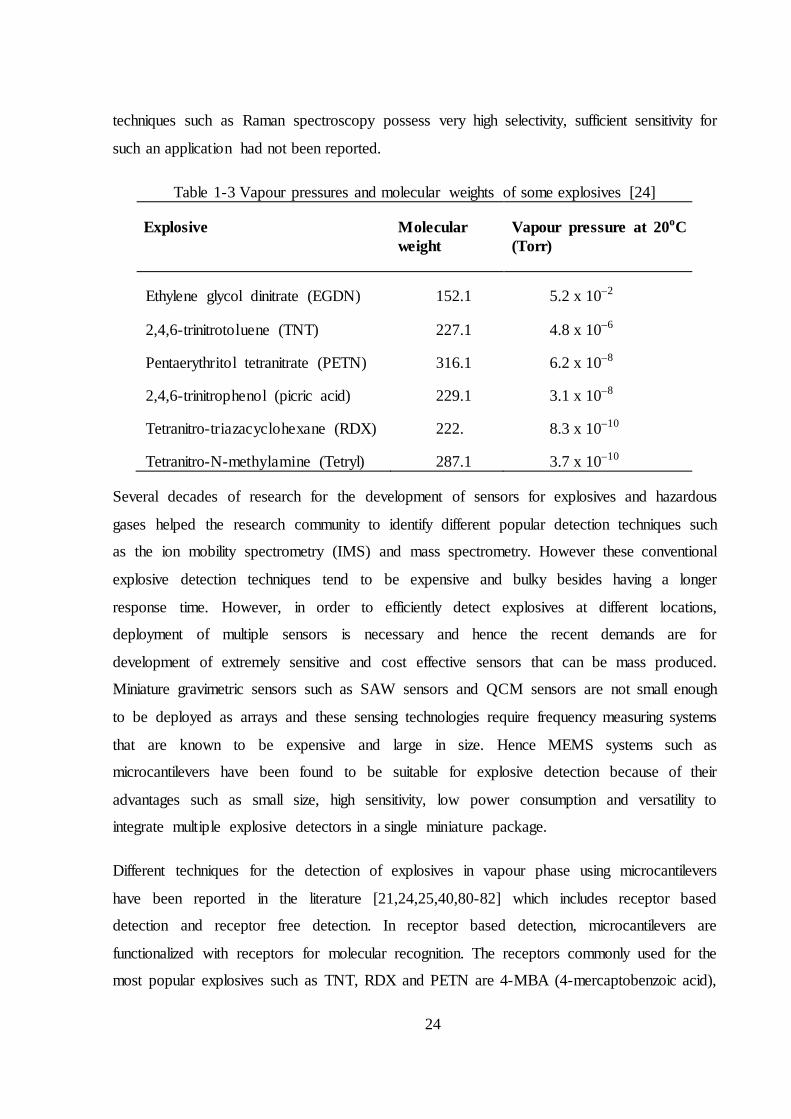
24
techniques such as Raman spectroscopy possess very high selectivity, sufficient sensitivity for
such an application had not been reported.
Table 1-3 Vapour pressures and molecular weights of some explosives [24]
Explosive Molecular weight
Vapour pressure at 20oC (Torr)
Ethylene glycol dinitrate (EGDN) 152.1 5.2 x 10⁻²
2,4,6-trinitrotoluene (TNT) 227.1 4.8 x 10⁻⁶
Pentaerythritol tetranitrate (PETN) 316.1 6.2 x 10⁻⁸
2,4,6-trinitrophenol (picric acid) 229.1 3.1 x 10⁻⁸
Tetranitro-triazacyclohexane (RDX) 222. 8.3 x 10⁻¹⁰
Tetranitro-N-methylamine (Tetryl) 287.1 3.7 x 10⁻¹⁰
Several decades of research for the development of sensors for explosives and hazardous
gases helped the research community to identify different popular detection techniques such
as the ion mobility spectrometry (IMS) and mass spectrometry. However these conventional
explosive detection techniques tend to be expensive and bulky besides having a longer
response time. However, in order to efficiently detect explosives at different locations,
deployment of multiple sensors is necessary and hence the recent demands are for
development of extremely sensitive and cost effective sensors that can be mass produced.
Miniature gravimetric sensors such as SAW sensors and QCM sensors are not small enough
to be deployed as arrays and these sensing technologies require frequency measuring systems
that are known to be expensive and large in size. Hence MEMS systems such as
microcantilevers have been found to be suitable for explosive detection because of their
advantages such as small size, high sensitivity, low power consumption and versatility to
integrate multiple explosive detectors in a single miniature package.
Different techniques for the detection of explosives in vapour phase using microcantilevers
have been reported in the literature [21,24,25,40,80-82] which includes receptor based
detection and receptor free detection. In receptor based detection, microcantilevers are
functionalized with receptors for molecular recognition. The receptors commonly used for the
most popular explosives such as TNT, RDX and PETN are 4-MBA (4-mercaptobenzoic acid),
25
SXFA (poly(1-(4-hydroxy-4-trifluoromethyl-5,5,5-trifluoro)pent-1-enyl)methylsiloxane)etc.
[24,83,84] and the functionalization procedure is based on the receptor and microcantilever
surface chemistry. The molecular recognition mechanisms in these cases are based on the
weak interactions that can be reversed making the microcantilever sensors reversible. Self-
assembled siloxane-based TNT-sensitive bi-layer are also reported to be in use with silicon
dioxide microcantilevers and are seen to be more stable than thiol based SAM such as 4-MBA
[85]. Another novel coating material, hexa-fluoro-isopropanol-functionalized mesoporous-
silica (HFMS) possessing ultra-high specific-surface-area was also been reported. This seems
to be one of the effective coating materials as it allows more specific-capture of a large
number of the very small TNT molecules [86]. All these receptors based on weak molecular
interactions enable sensitive and reversible mechanisms for detection of explosive vapours.
However, reversible receptor-based approaches are known to lack selectivity and therefore
identifying highly specific receptor molecules to improve selectivity in detection of explosive
is an on-going research. Receptor free techniques such as , differential thermal analysis that
produces unique and reproducible thermal response patterns for different molecules [80][81]
and photothermal deflection spectroscopy (PDS) [22] were introduced to bring selectivity
along with sensitivity and sensor reversibility. Both these techniques utilized extremely high
thermal sensitivity of a bimaterial cantilever.
1.4 Objectives and scope of the work
Based on the literature survey that has been carried out on microcantilever based bio/chemical
sensors, it has been found that the demand for low cost, highly sensitive and handheld
portable microcantilever bio/chemical sensor platform might be fulfilled by using SU-8
microcantilevers with integrated piezoresistive transduction. The selection of the
piezoresistive layer should be in such a way that it possesses high gauge factor, low Young’s
modulus(comparable to that of SU-8), process compatibility with SU-8 and patternability
using standard processes followed in microfabrication.
As per the available literature on piezoresistive SU-8 microcantilevers summarized in section
1.2.4, SU-8 microcantilevers with SU-8/CB strain sensor could offer very good sensitivity due
to large value of K/E for this composite structure. As the piezoresistor is SU-8 based, the
26
process compatibility and cost effectiveness could be additional merits. However, the
literature could only convey a basic proof of concept of integrating SU-8/CB nanocomposite
as piezoresistor. Hence, investigating the scope of improving the sensitivity of these sensors
and evaluating their performance for bio/chemical sensing applications could be an interesting
topic of research. It can be hypothesized that the performance of SU-8 nanocomposite
microcantilevers can be improved by using well dispersed and optimized composite of CB in
SU-8 with desirable electrical, mechanical and piezoresistive properties and by improving the
design of the microcantilever.
SU-8 being an organic material, integration of a strain sensitive conducting polymer or
organic layer with very good gauge factor for electrical transduction in SU-8 microcantilevers
could also be explored. As discussed section 1.2.4.1, pentacene is an organic semiconductor
with proven capability as strain sensor though not in use for MEMS based sensors. Its low
temperature deposition process would make it compatible for deposition on polymer
structures. In line with the previously reported configuration (pentacene as channel material
in OFET) of large area strain sensors using pentacene, pentacene based OFET could be
integrated with SU-8 microcantilevers. This might be a cost effective counterpart of the
MOSFET embedded silicon nitride microcantilevers that were demonstrated to show better
performances over piezoresistive microcantilevers [50].
Based on these hypotheses, the objectives and scope of this thesis could be listed as below:-
1. Explore the different possibilities of improving the performances of SU-8
nanomechanical cantilever sensors with integrated nanocomposite as piezoresistor.
(i) Prepare SU-8/CB nanocomposites to study their thin film and electrical conduction
behaviour in order to integrate the nanocomposite as piezoresistive layer with SU-8
microcantilevers.
(ii) Fabrication process development for polymer nanocomposite microcantilevers with
minimum possible beam and piezoresistive layer thicknesses. This approach could
lead to fabrication of SU-8/CB nanocomposite microcantilevers with improved
sensitivity.
(iii) A systematic characterization of the SU-8/CB nanocomposite in order to
understand its electrical and mechanical characteristics. This is required to decide
the optimal range of concentration of CB filler in SU-8 in order to improve the

27
overall performance of the polymer nanocomposite microcantilever sensor in terms
of its sensitivity and device variability
(iv) Fabrication of SU-8 microcantilevers (using a microcantilever design with
minimum possible fabrication process complexity chosen for surface stress
measurements) with integrated SU-8 nanocomposite prepared with optimum filler
concentration and improved dispersion technique.
(v) Systematic characterization of fabricated nanocomposite microcantilevers for their
mechanical, electrical and electromechanical and noise parameters so as to
benchmark their performances with other microcantilever based bio/chemical
sensors.
(vi) Application development for these nanocomposite microcantilevers in the field of
chemical sensing, more specifically for detection of explosive vapours.
2. Explore a novel electrical transduction technique for SU-8 nanomechanical cantilever
sensors by integrating a strain sensitive organic field effect transistor (OFET) with a
polymer nanomechanical cantilever. This device could be thought of as a low cost
polymer counterpart of a similar reported device in silicon, MOSFET embedded
microcantilever that was discussed in the literature review. The ways of integrating the
OFET with an SU-8 microcantilever could be evolved by evaluating the performance of
OFET with polymer dielectric compatible with SU-8 processes and by analysing process
compatibility for fabricating these two devices (OFET and SU-8 microcantilever). With
optimizations in the unit process level, an SU-8 nanomechanical cantilever device with
embedded OFET (here after named as ‘Organic CantiFET’) could be fabricated and
characterized.
Though the focus of this thesis has been on the development of SU-8 nanomechanical
cantilever sensors with integrated electrical read out, simple single layer SU-8
microcantilevers for optical transduction could also be developed in order to get familiarized
with SU-8 microcantilever fabrication process and to optimize the unit processes involved in
the fabrication of SU-8 based microcantilevers. In addition to this, due to ease in
implementing such a simple sensor in a laboratory environment, this would also aid in
application development using SU-8 microcantilever platforms.
28
1.5 Thesis Organization
This thesis is organized in six chapters.
Chapter 1 i.e. the present chapter provided a detailed introduction and motivation for this research
supported by literature survey along with the list of objectives and scope of the research work
presented this thesis.
Chapter 2 gives a basic understanding of the polymer SU-8 and microfabrication processing.
Design and fabrication of single layer SU-8 microcantilevers for optical lever transduction is
also covered in this chapter. The microfabrication process development for SU-8
microcantilevers presented in this chapter forms the base for the development of multilayer
SU-8 microcantilevers that are discussed in the following chapters. Mechanical
characterization of SU-8 microcantilevers and application development for explosive vapour
detections using a standard atomic force microscope (AFM) for optical transduction also has
been discussed in this chapter.
Chapter 3 deals with the development of polymer nanomechanical cantilevers with embedded
polymer/nanoparticle composite for electrical transduction. This chapter covers the (i)
systematic characterization of the piezoresistor material, SU-8/Carbon black composite for its
thin film, mechanical and electrical characterizations (ii) design and fabrication process
development for SU-8 nanocomposite microcantilevers and (iii) various characterizations of
the fabricated nanocomposite nanomechanical cantilever devices for evaluating their
performances for bio/chemical sensing applications.
In Chapter 4, application development for explosive detection using polymer nanocomposite
microcantilevers is discussed.
In Chapter 5, polymer nanomechanical cantilever sensor with a novel transduction scheme
using an embedded strain sensitive organic field effect transistor (OFET) inside an SU-8
microcantilever structure is explored. In this chapter, fabrication process development for this
device and various characterizations of these devices to benchmark their performances with
other existing polymer microcantilever devices have been covered in detail.

29
Chapter 6 finally concludes this research work. Results obtained in the previous chapters are
summarized based on which some future recommendations are made is 8also presented in this
chapter.
30
Chapter 2
SU-8 Microcantilevers for Optical Transduction
2.1 Introduction
The focus of the research work in this thesis has been on the development of novel SU-8
nanomechanical cantilever sensors with integrated electrical readout for bio/chemical sensing
applications. However, the microfabrication process integration for such SU-8
microcantilevers could be complex as these microcantilevers would be multilayer composite
structure that accommodates the in-situ electrical transduction scheme. The unit processes had
to be optimized before the final process integration for these SU-8 microcantilevers.
Development of a fabrication process for single layer SU-8 microcantilevers could be
considered as the first milestone as this would aid in establishing the process scheme and the
main unit processes for SU-8 microcantilevers using the available materials in the given
laboratory conditions. In principle, these single layer SU-8 microcantilevers could be used as
sensors with optical transduction that are very similar to atomic force microscope probes.
Moreover, the development of these simple SU-8 cantilever sensors might also help in testing
the feasibility of using SU-8 microcantilevers for various sensing applications.
This chapter provides an overview of SU-8 material, processing, fabrication of single layer
SU-8 microcantilevers for optical transduction, device characterization and finally application
31
development using these SU-8 microcantilevers for detection of explosive molecules in
vapour phase.
2.2 SU-8 material properties and processing
SU-8 is an epoxy based, negative tone, near-UV sensitive photoresist developed by IBM
Research [30,32]. It has a great potential for high aspect ratio structures [31] . It can be spin
coated to thicknesses in range of few hundreds of nm to few mm. The very low Young's
modulus (~ 4-5 GPa) and the ease of processing makes this photoresist a very promising
material for the fabrication of microcantilever sensor with very good sensitivity.
SU-8 monomer has eight epoxy groups . Such molecules are capable of being converted to a
thermoset form or three-dimensional network structure. This process is called curing or
crosslinking. So these eight epoxy groups are responsible for the crosslinking with other
monomers to form a polymer with the highest known crosslinking density.
SU-8 is commercially available from Microchem [87] and comes in two series which differs
from each other by the type of solvent present. The SU-8 formulations used in this research
work belong to SU-8 2000 series with cyclopentanone as the solvent. SU-8 resist contains a
monomer, a solvent and a photo-initiator which is triarylsulfonium salt that has the property
of disintegrating when exposed to light. One of the disintegration products is strong Lewis
acid that initiates the crosslinking chain reaction between SU-8 monomers and this
mechanism is termed as cationic polymerization [88,89].
The typical processing sequence for microfabrication of SU-8 structures is illustrated in
Figure 2.1.
1. Dehydration bake
The cleaned or pre-treated (cleaning or pre-treatment decided based on the history of the
sample) sample is kept for dehydration bake in an oven or a hotplate at 110oC. This ensures
removal of moisture from the sample surface.
32
2. Spin coating
The formation of SU-8 layer is done by spin coating of SU-8 on the sample using a standard
spinner. The thicknesses of the spin coated SU-8 layers are determined by the viscosity of the
resist and the spin coating parameters such as speed (rpm) and time. In the case of thick SU-8
layers, the thickness depends on the quantity of photoresist initially placed on the substrate for
spin coating. SU-8 2000 series comes with different formulations that have different solvent
content and hence different viscosities. For example, SU-8 2000.5 ,SU-8 2002 and SU-8 2100
spin coated at 3000 rpm for 35 seconds are expected to form SU-8 layers of thicknesses of
500 nm, 2 m and 100 m respectively. In the case of high viscous SU-8 formulations, spin
coating process imparts edge bead. This can be minimized by leaving the spin coated sample
for a few minutes on a levelled surface at room temperature. As this is done at room
temperature, the solvent present in the resist allows reflow of SU-8 and hence minimises the
edge bead.
3. Prebake
Prebake or soft bake step is performed for removing solvent from the SU-8 layer after spin
coating. It is performed by slowly heating the substrate on a levelled hotplate. Microchem
recommends a two-step baking process at 65oC and 95oC with the baking times decided based
on the SU-8 thickness. As reported earlier in [90], over baking is less critical than under
baking. The glass transition temperature (Tg) of SU-8 is about 50oC, and so the prebake
temperature of SU-8 being greater than this, reflow of the resist occurs during initial few
minutes of prebake. In order to produce smooth, uniform coating of SU-8 on the substrate, it
is very critical to have a levelled hotplate.
4. UV Exposure
As per the catalytic polymerization of SU-8, the basic source of crosslinking of SU-8 is the
Lewis acid that has been generated during UV exposure. So this is one of the most critical
steps that can decide the quality of the final SU-8 structure aimed for. Exposure doses
(defined as product of UV lamp intensity and duration of exposure) need to be optimized
depending upon the formulation of SU-8 and prebaking history. Optical mask aligners with
UV sources having wavelengths near to 365 nm are used for this process. Light absorbance in
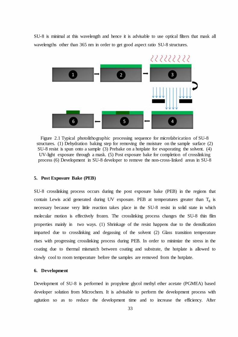
33
SU-8 is minimal at this wavelength and hence it is advisable to use optical filters that mask all
wavelengths other than 365 nm in order to get good aspect ratio SU-8 structures.
Figure 2.1 Typical photolithographic processing sequence for microfabrication of SU-8 structures. (1) Dehydration baking step for removing the moisture on the sample surface (2) SU-8 resist is spun onto a sample (3) Prebake on a hotplate for evaporating the solvent. (4) UV-light exposure through a mask. (5) Post exposure bake for completion of crosslinking process (6) Development in SU-8 developer to remove the non-cross-linked areas in SU-8
5. Post Exposure Bake (PEB)
SU-8 crosslinking process occurs during the post exposure bake (PEB) in the regions that
contain Lewis acid generated during UV exposure. PEB at temperatures greater than Tg is
necessary because very little reaction takes place in the SU-8 resist in solid state in which
molecular motion is effectively frozen. The crosslinking process changes the SU-8 thin film
properties mainly in two ways. (1) Shrinkage of the resist happens due to the densification
imparted due to crosslinking and degassing of the solvent (2) Glass transition temperature
rises with progressing crosslinking process during PEB. In order to minimize the stress in the
coating due to thermal mismatch between coating and substrate, the hotplate is allowed to
slowly cool to room temperature before the samples are removed from the hotplate.
6. Development
Development of SU-8 is performed in propylene glycol methyl ether acetate (PGMEA) based
developer solution from Microchem. It is advisable to perform the development process with
agitation so as to reduce the development time and to increase the efficiency. After
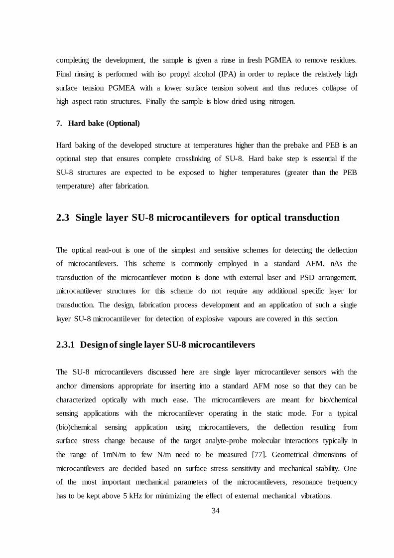
34
completing the development, the sample is given a rinse in fresh PGMEA to remove residues.
Final rinsing is performed with iso propyl alcohol (IPA) in order to replace the relatively high
surface tension PGMEA with a lower surface tension solvent and thus reduces collapse of
high aspect ratio structures. Finally the sample is blow dried using nitrogen.
7. Hard bake (Optional)
Hard baking of the developed structure at temperatures higher than the prebake and PEB is an
optional step that ensures complete crosslinking of SU-8. Hard bake step is essential if the
SU-8 structures are expected to be exposed to higher temperatures (greater than the PEB
temperature) after fabrication.
2.3 Single layer SU-8 microcantilevers for optical transduction
The optical read-out is one of the simplest and sensitive schemes for detecting the deflection
of microcantilevers. This scheme is commonly employed in a standard AFM. nAs the
transduction of the microcantilever motion is done with external laser and PSD arrangement,
microcantilever structures for this scheme do not require any additional specific layer for
transduction. The design, fabrication process development and an application of such a single
layer SU-8 microcantilever for detection of explosive vapours are covered in this section.
2.3.1 Design of single layer SU-8 microcantilevers
The SU-8 microcantilevers discussed here are single layer microcantilever sensors with the
anchor dimensions appropriate for inserting into a standard AFM nose so that they can be
characterized optically with much ease. The microcantilevers are meant for bio/chemical
sensing applications with the microcantilever operating in the static mode. For a typical
(bio)chemical sensing application using microcantilevers, the deflection resulting from
surface stress change because of the target analyte-probe molecular interactions typically in
the range of 1mN/m to few N/m need to be measured [77]. Geometrical dimensions of
microcantilevers are decided based on surface stress sensitivity and mechanical stability. One
of the most important mechanical parameters of the microcantilevers, resonance frequency
has to be kept above 5 kHz for minimizing the effect of external mechanical vibrations.
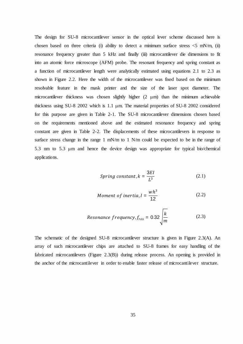
35
The design for SU-8 microcantilever sensor in the optical lever scheme discussed here is
chosen based on three criteria (i) ability to detect a minimum surface stress <5 mN/m, (ii)
resonance frequency greater than 5 kHz and finally (iii) microcantilever die dimensions to fit
into an atomic force microscope (AFM) probe. The resonant frequency and spring constant as
a function of microcantilever length were analytically estimated using equations 2.1 to 2.3 as
shown in Figure 2.2. Here the width of the microcantilever was fixed based on the minimum
resolvable feature in the mask printer and the size of the laser spot diameter. The
microcantilever thickness was chosen slightly higher (2 m) than the minimum achievable
thickness using SU-8 2002 which is 1.1 m. The material properties of SU-8 2002 considered
for this purpose are given in Table 2-1. The SU-8 microcantilever dimensions chosen based
on the requirements mentioned above and the estimated resonance frequency and spring
constant are given in Table 2-2. The displacements of these microcantilevers in response to
surface stress change in the range 1 mN/m to 1 N/m could be expected to be in the range of
5.3 nm to 5.3 m and hence the device design was appropriate for typical bio/chemical
applications.
푆푝푟푖푛푔푐표푛푠푡푎푛푡, 푘 =3퐸퐼퐿
(2.1)
푀표푚푒푛푡표푓푖푛푒푟푡푖푎, 퐼 =
푤ℎ12
(2.2)
푅푒푠표푛푎푛푐푒푓푟푒푞푢푒푛푐푦, 푓 = 0.32
푘푚
(2.3)
The schematic of the designed SU-8 microcantilever structure is given in Figure 2.3(A). An
array of such microcantilever chips are attached to SU-8 frames for easy handling of the
fabricated microcantilevers (Figure 2.3(B)) during release process. An opening is provided in
the anchor of the microcantilever in order to enable faster release of microcantilever structure.
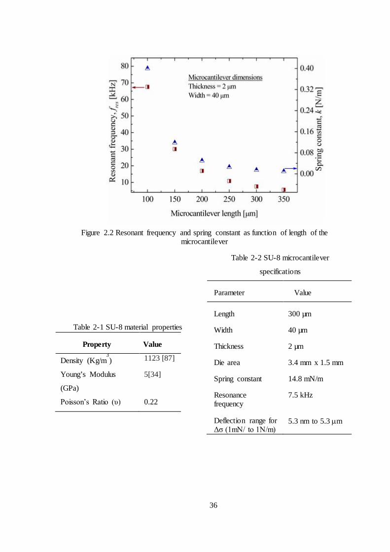
36
Figure 2.2 Resonant frequency and spring constant as function of length of the
microcantilever
Table 2-1 SU-8 material properties
Property Value
Density (Kg/m3) 1123 [87]
Young’s Modulus
(GPa)
5[34]
Poisson’s Ratio (υ) 0.22
Table 2-2 SU-8 microcantilever
specifications
Parameter Value
Length 300 µm
Width 40 µm
Thickness 2 µm
Die area 3.4 mm x 1.5 mm
Spring constant 14.8 mN/m
Resonance frequency
7.5 kHz
Deflection range for Δσ (1mN/ to 1N/m)
5.3 nm to 5.3 m
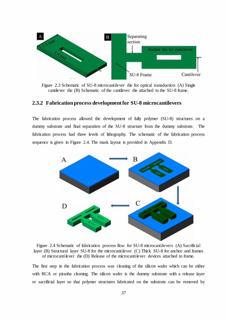
37
Figure 2.3 Schematic of SU-8 microcantilever die for optical transduction (A) Single
cantilever die (B) Schematic of the cantilever die attached to the SU-8 frame.
2.3.2 Fabrication process development for SU-8 microcantilevers
The fabrication process allowed the development of fully polymer (SU-8) structures on a
dummy substrate and final separation of the SU-8 structure from the dummy substrate. The
fabrication process had three levels of lithography. The schematic of the fabrication process
sequence is given in Figure 2.4. The mask layout is provided in Appendix D.
Figure 2.4 Schematic of fabrication process flow for SU-8 microcantilevers (A) Sacrificial
layer (B) Structural layer SU-8 for the microcantilever (C) Thick SU-8 for anchor and frames of microcantilever die (D) Release of the microcantilever devices attached to frame.
The first step in the fabrication process was cleaning of the silicon wafer which can be either
with RCA or piranha cleaning. The silicon wafer is the dummy substrate with a release layer
or sacrificial layer so that polymer structures fabricated on the substrate can be removed by

38
etching a sacrificial layer. Each of the unit processes in the fabrication of these
microcantilevers is detailed below. Though the dummy substrate considered in this research
work was silicon wafer, in principle the substrate could be glass substrate or polymeric
substrates. However, the substrates should possess certain prerequisites such as the substrate
surface roughness as minimal as possible, substrate dimensions compatible for the processing
equipment to be used for the fabrication process and the stability of the substrate material
during the entire processing.
(A) Sacrificial layer
The essential qualities of release or sacrificial layers are:-
1. It should be possible to coat a sufficiently thick layer of the release layer material so
that it ensures the easy access for the etchant chemical to perform under etch reaction
that would not be diffusion limited. An efficiently progressing under etch process aids
in easy release of the structure from the substrate.
2. The sacrificial layer should possess uniform thickness and minimum surface
roughness. This is important because any non-uniformity or roughness on the
sacrificial layer could get transferred to the microcantilever structural layer.
3. The surface properties of the sacrificial layer should enable uniform spin coating of
SU-8 layer and provide good adhesion for SU-8 layer without delamination or peeling
off.
4. The etching reaction should be fast enough for easy release of the SU-8 structure from
the underlying substrate.
5. The etchant for the sacrificial layer should not attack the crosslinked SU-8.
A comparative study on different sacrificial layer materials such as metals (Al,Cr/Au and Cu)
and polymers ( polymethylmethacrylate, polyimide and poly-styrene) were reported [91]. Out
of the metals, Cu provided better results. However, they were the best choice as sacrificial
layers for SU-8 structures with planar dimensions up to 200 m. Polymers were shown to be
good as sacrificial layers for SU-8 structures up to 600 m. But there are certain issues that
were reported such as poor adhesion between the polymeric sacrificial layer and SU-8 and the
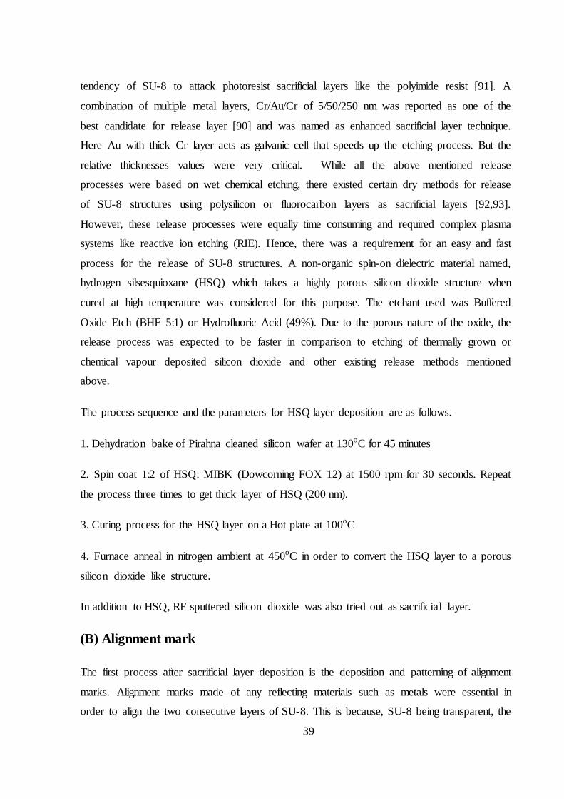
39
tendency of SU-8 to attack photoresist sacrificial layers like the polyimide resist [91]. A
combination of multiple metal layers, Cr/Au/Cr of 5/50/250 nm was reported as one of the
best candidate for release layer [90] and was named as enhanced sacrificial layer technique.
Here Au with thick Cr layer acts as galvanic cell that speeds up the etching process. But the
relative thicknesses values were very critical. While all the above mentioned release
processes were based on wet chemical etching, there existed certain dry methods for release
of SU-8 structures using polysilicon or fluorocarbon layers as sacrificial layers [92,93].
However, these release processes were equally time consuming and required complex plasma
systems like reactive ion etching (RIE). Hence, there was a requirement for an easy and fast
process for the release of SU-8 structures. A non-organic spin-on dielectric material named,
hydrogen silsesquioxane (HSQ) which takes a highly porous silicon dioxide structure when
cured at high temperature was considered for this purpose. The etchant used was Buffered
Oxide Etch (BHF 5:1) or Hydrofluoric Acid (49%). Due to the porous nature of the oxide, the
release process was expected to be faster in comparison to etching of thermally grown or
chemical vapour deposited silicon dioxide and other existing release methods mentioned
above.
The process sequence and the parameters for HSQ layer deposition are as follows.
1. Dehydration bake of Pirahna cleaned silicon wafer at 130oC for 45 minutes
2. Spin coat 1:2 of HSQ: MIBK (Dowcorning FOX 12) at 1500 rpm for 30 seconds. Repeat
the process three times to get thick layer of HSQ (200 nm).
3. Curing process for the HSQ layer on a Hot plate at 100oC
4. Furnace anneal in nitrogen ambient at 450oC in order to convert the HSQ layer to a porous
silicon dioxide like structure.
In addition to HSQ, RF sputtered silicon dioxide was also tried out as sacrificial layer.
(B) Alignment mark
The first process after sacrificial layer deposition is the deposition and patterning of alignment
marks. Alignment marks made of any reflecting materials such as metals were essential in
order to align the two consecutive layers of SU-8. This is because, SU-8 being transparent, the
40
patterns on first layer of SU-8 of thickness 2 m could be very difficult to resolve after the
subsequent spin coat and bake processes for thick SU-8 2100. Here, alignment marks made of
30 nm of gold were used. A thin layer (5 nm) of chromium or titanium could be used as
adhesion promoting layer for gold. The patterning process followed was standard lift-off
process (mask # 1). This step is not shown in the process sequence as the alignment marks
were global alignment marks for the wafer and not part of the device structure.
(C) SU-8 layer for cantilever structural layer
Next step is the patterning of SU-8 layer of 2 m that defined the structural layer of the
microcantilever along with an extension of the layer to microcantilever anchors and frames.
For this, the wafer was kept for dehydration bake step at 110oC for 30 minutes. Then SU-8
2002 was spin coated at 500 rpm for 5 seconds and then at 3000 rpm for 35 seconds with
proper acceleration. Subsequently the sample was kept for prebake (PB) which was a two-step
baking on a hotplate maintained at 70oC for 3 minutes and 90oC for 7 minutes. The SU-8
layer was subjected to UV exposure through mask # 2 for 10 seconds in Karl Suss MJB 3
standard mask aligner. This was followed by post exposure bake (PEB) which was again a
two-step bake at 70oC for 2 minutes and 90oC for 5 minutes. Then the development in SU-8
developer for 1 minute followed by rinse in IPA was performed. The wafer was blow dried
using nitrogen gun.
(D) Thick layer of SU-8 for microcantilever anchor and holding frame
SU-8 2100 was used for forming anchor and frame layers with thickness greater than 220
microns. The processes were very similar to SU-8 2002 process explained earlier with an
increase in bake and exposure timings.
The optical micrograph of the SU-8 structures on wafer after this process is shown in Figure
2.5(A). Lot of stress lines were observed in the structure.
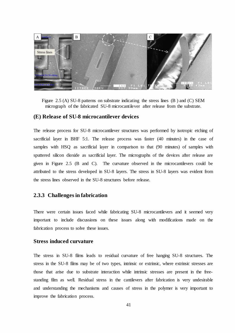
41
Figure 2.5 (A) SU-8 patterns on substrate indicating the stress lines (B ) and (C) SEM micrograph of the fabricated SU-8 microcantilever after release from the substrate.
(E) Release of SU-8 microcantilever devices
The release process for SU-8 microcantilever structures was performed by isotropic etching of
sacrificial layer in BHF 5:1. The release process was faster (40 minutes) in the case of
samples with HSQ as sacrificial layer in comparison to that (90 minutes) of samples with
sputtered silicon dioxide as sacrificial layer. The micrographs of the devices after release are
given in Figure 2.5 (B and C). The curvature observed in the microcantilevers could be
attributed to the stress developed in SU-8 layers. The stress in SU-8 layers was evident from
the stress lines observed in the SU-8 structures before release.
2.3.3 Challenges in fabrication
There were certain issues faced while fabricating SU-8 microcantilevers and it seemed very
important to include discussions on these issues along with modifications made on the
fabrication process to solve these issues.
Stress induced curvature
The stress in SU-8 films leads to residual curvature of free hanging SU-8 structures. The
stress in the SU-8 films may be of two types, intrinsic or extrinsic, where extrinsic stresses are
those that arise due to substrate interaction while intrinsic stresses are present in the free-
standing film as well. Residual stress in the cantilevers after fabrication is very undesirable
and understanding the mechanisms and causes of stress in the polymer is very important to
improve the fabrication process.
42
The thermal stress may be due to difference in coefficient of thermal expansion between the
substrate Si and SU-8. So during cooling stage after PEB, it develops tensile stress [94].
Before crosslinking, SU-8 is stress free since the monomers are not constrained to move by
the polymer lattice. So stress is developed mainly in the thermal cycle after exposure. This
can be reduced by reducing the PEB temperature and slow ramp down to room temperature
after the second step of PEB. However if thermal stresses are uniform across the thickness of
SU-8 layer, it should not curve after being released.
The stress in thick SU-8 anchor layer could be the major cause of curvature seen in
microcantilevers. This origin of stress could be mainly controlled by optimizing the
combination of UV exposure dose and PEB. When SU-8 is baked on a hot plate, a linear
temperature gradient through the SU-8 film could be expected to exist [95]. As a result, the
bottom layers of the SU-8 film will be curing at higher temperatures than the top surface. As
per the theory given in [95], with moderate UV doses, the crosslinking density through the
SU-8 film and hence stress can be altered with baking parameters. Compliant structures may
have a negative, positive or zero curvature. However, with very large UV doses, the catalyst
concentration through the film is at or near a maximum, and the thermal gradient from baking
on a hot plate dominates stress behaviour of the film. The bottom layers of film are expected
to be at a higher temperature than the top layers. So the crosslinking density would be higher
near the bottom than at the top. Feng et.al.in [96] reported that thermal expansion of epoxies
depends on the extent of crosslinking. Hence when an SU-8 film with a through thickness
gradient of crosslinking density is cooled, the bottom contracts less than the top, resulting in
less tensile strain at the bottom and more at the top. This gradient in strains causes the SU-8
hanging structures to curl up for all baking times.
Another observation was that the bending of the microcantilevers and the frames were more
in the case of those with thicker SU-8 pad layer. This may also be due to non-uniform
shrinkage of thick SU-8 along the thickness during cross-linking. And this effect is more
severe in thicker pads. This happens because the bottom side is getting heated up more during
hot plate bake. So a possible solution may be to reduce the thickness of anchor layer of SU-8.
However in order to have uniform crosslinking of SU-8, it is good to reduce the PEB
temperature and increase the time of PEB.
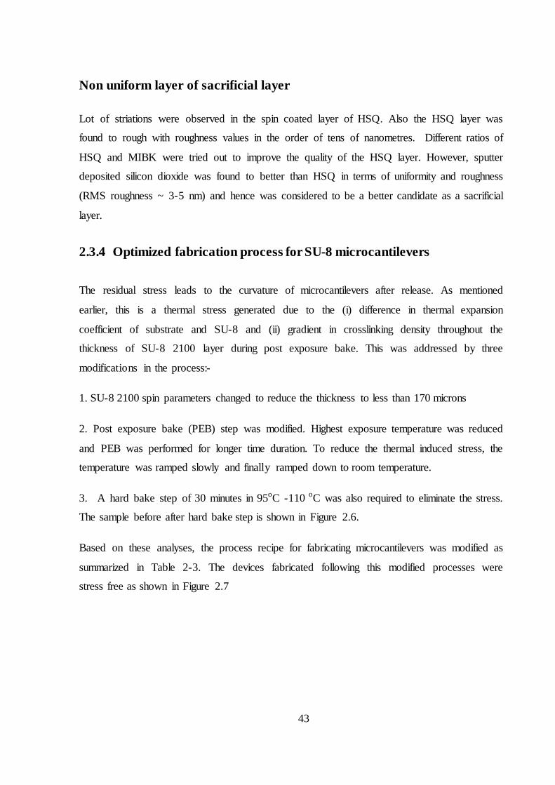
43
Non uniform layer of sacrificial layer
Lot of striations were observed in the spin coated layer of HSQ. Also the HSQ layer was
found to rough with roughness values in the order of tens of nanometres. Different ratios of
HSQ and MIBK were tried out to improve the quality of the HSQ layer. However, sputter
deposited silicon dioxide was found to better than HSQ in terms of uniformity and roughness
(RMS roughness ~ 3-5 nm) and hence was considered to be a better candidate as a sacrificial
layer.
2.3.4 Optimized fabrication process for SU-8 microcantilevers
The residual stress leads to the curvature of microcantilevers after release. As mentioned
earlier, this is a thermal stress generated due to the (i) difference in thermal expansion
coefficient of substrate and SU-8 and (ii) gradient in crosslinking density throughout the
thickness of SU-8 2100 layer during post exposure bake. This was addressed by three
modifications in the process:-
1. SU-8 2100 spin parameters changed to reduce the thickness to less than 170 microns
2. Post exposure bake (PEB) step was modified. Highest exposure temperature was reduced
and PEB was performed for longer time duration. To reduce the thermal induced stress, the
temperature was ramped slowly and finally ramped down to room temperature.
3. A hard bake step of 30 minutes in 95oC -110 oC was also required to eliminate the stress.
The sample before after hard bake step is shown in Figure 2.6.
Based on these analyses, the process recipe for fabricating microcantilevers was modified as
summarized in Table 2-3. The devices fabricated following this modified processes were
stress free as shown in Figure 2.7
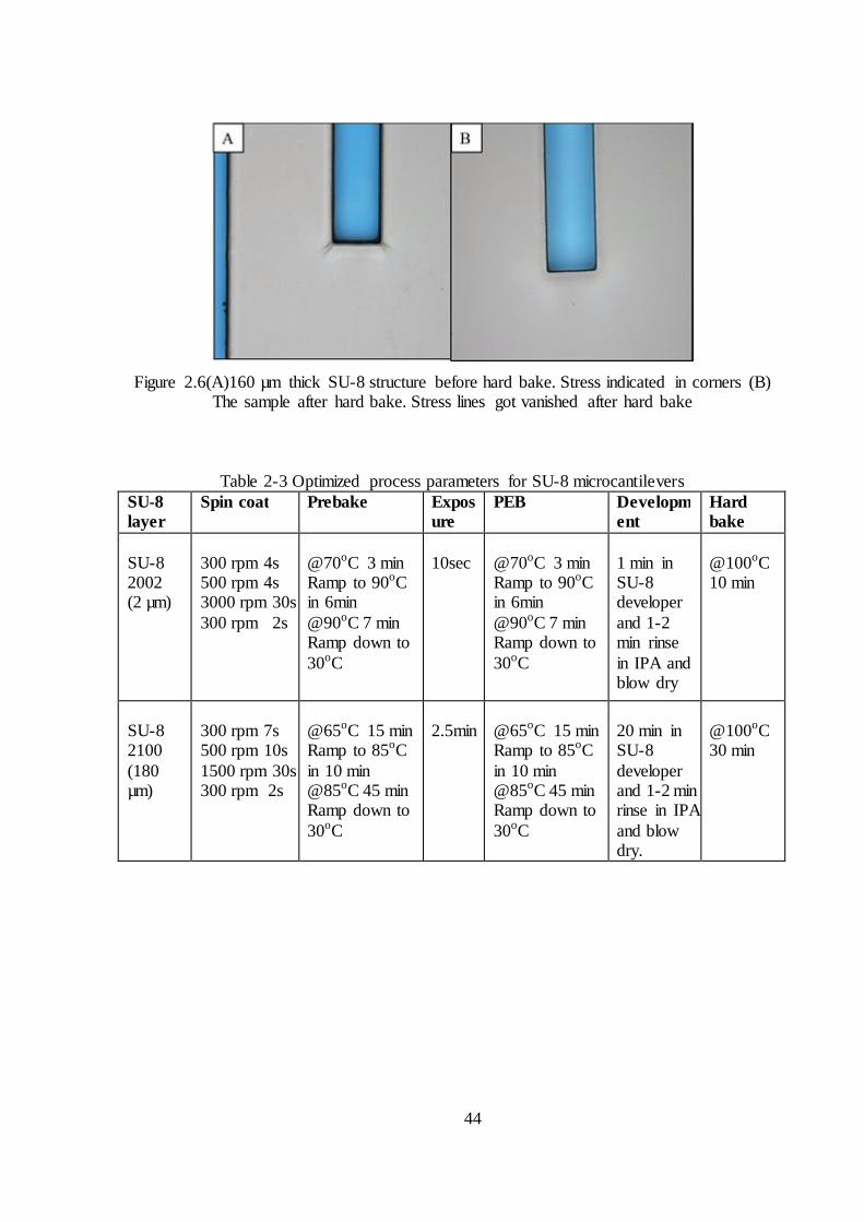
44
Figure 2.6(A)160 µm thick SU-8 structure before hard bake. Stress indicated in corners (B)
The sample after hard bake. Stress lines got vanished after hard bake
Table 2-3 Optimized process parameters for SU-8 microcantilevers SU-8 layer
Spin coat
Prebake Exposure
PEB Development
Hard bake
SU-8 2002 (2 µm)
300 rpm 4s 500 rpm 4s 3000 rpm 30s 300 rpm 2s
@70oC 3 min Ramp to 90oC in 6min @90oC 7 min Ramp down to 30oC
10sec
@70oC 3 min Ramp to 90oC in 6min @90oC 7 min Ramp down to 30oC
1 min in SU-8 developer and 1-2 min rinse in IPA and blow dry
@100oC 10 min
SU-8 2100 (180 µm)
300 rpm 7s 500 rpm 10s 1500 rpm 30s 300 rpm 2s
@65oC 15 min Ramp to 85oC in 10 min @85oC 45 min Ramp down to 30oC
2.5min
@65oC 15 min Ramp to 85oC in 10 min @85oC 45 min Ramp down to 30oC
20 min in SU-8 developer and 1-2 min rinse in IPA and blow dry.
@100oC 30 min

45
Figure 2.7 SU-8 microcantilevers fabricated after optimization process (A) SU-8 frames holding arrays of SU-8 microcantilevers. These devices were coated with gold. (B) Optical micrograph of one of the microcantilevers (C) SEM micrograph indicating the stress free
nature of the microcantilevers
2.3.5 Characterization
The dynamic characterization of these microcantilevers had to be performed in order to find
out their resonant frequency. For this purpose, a PicoSPM II, (Agilent) AFM system was
employed. The typical laser diameter is approximately 35 μm and the minimum detectable
deflection of cantilevers is in the sub-nanometer range.
SU-8 microcantilevers to be characterized using AFM were coated with 45 nm of gold for
providing a reflecting surface for laser beam. 10 nm of chromium was used as the adhesion
promoting layer. Microcantilever chip was mounted on acoustic AC mode nose of the AFM
scanner. The laser was focused near the free end of the cantilever and the position of the
photo detector of AFM was adjusted to get maximum output signal. In acoustic AC mode, the
piezoelectric stack inside the scanner excites the microcantilever to oscillate and the laser
beam reflected from the oscillating microcantilever gets deflected in a regular pattern over a
photodiode array, generating a sinusoidal electronic signal. The root mean square voltage
value for this signal is displayed on the display unit. Microcantilever was excited with signals
of different frequencies ranging from 5 kHz to 100 kHz. The drive signal was gradually
increased from 20% of the maximum possible value, in order to maximize the response
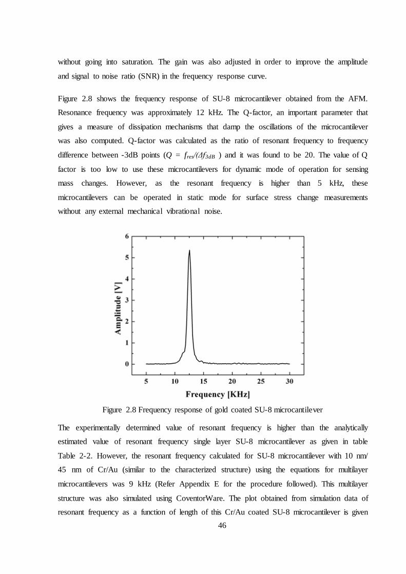
46
without going into saturation. The gain was also adjusted in order to improve the amplitude
and signal to noise ratio (SNR) in the frequency response curve.
Figure 2.8 shows the frequency response of SU-8 microcantilever obtained from the AFM.
Resonance frequency was approximately 12 kHz. The Q-factor, an important parameter that
gives a measure of dissipation mechanisms that damp the oscillations of the microcantilever
was also computed. Q-factor was calculated as the ratio of resonant frequency to frequency
difference between -3dB points (Q = fres/(Δf3dB ) and it was found to be 20. The value of Q
factor is too low to use these microcantilevers for dynamic mode of operation for sensing
mass changes. However, as the resonant frequency is higher than 5 kHz, these
microcantilevers can be operated in static mode for surface stress change measurements
without any external mechanical vibrational noise.
Figure 2.8 Frequency response of gold coated SU-8 microcantilever
The experimentally determined value of resonant frequency is higher than the analytically
estimated value of resonant frequency single layer SU-8 microcantilever as given in table
Table 2-2. However, the resonant frequency calculated for SU-8 microcantilever with 10 nm/
45 nm of Cr/Au (similar to the characterized structure) using the equations for multilayer
microcantilevers was 9 kHz (Refer Appendix E for the procedure followed). This multilayer
structure was also simulated using CoventorWare. The plot obtained from simulation data of
resonant frequency as a function of length of this Cr/Au coated SU-8 microcantilever is given
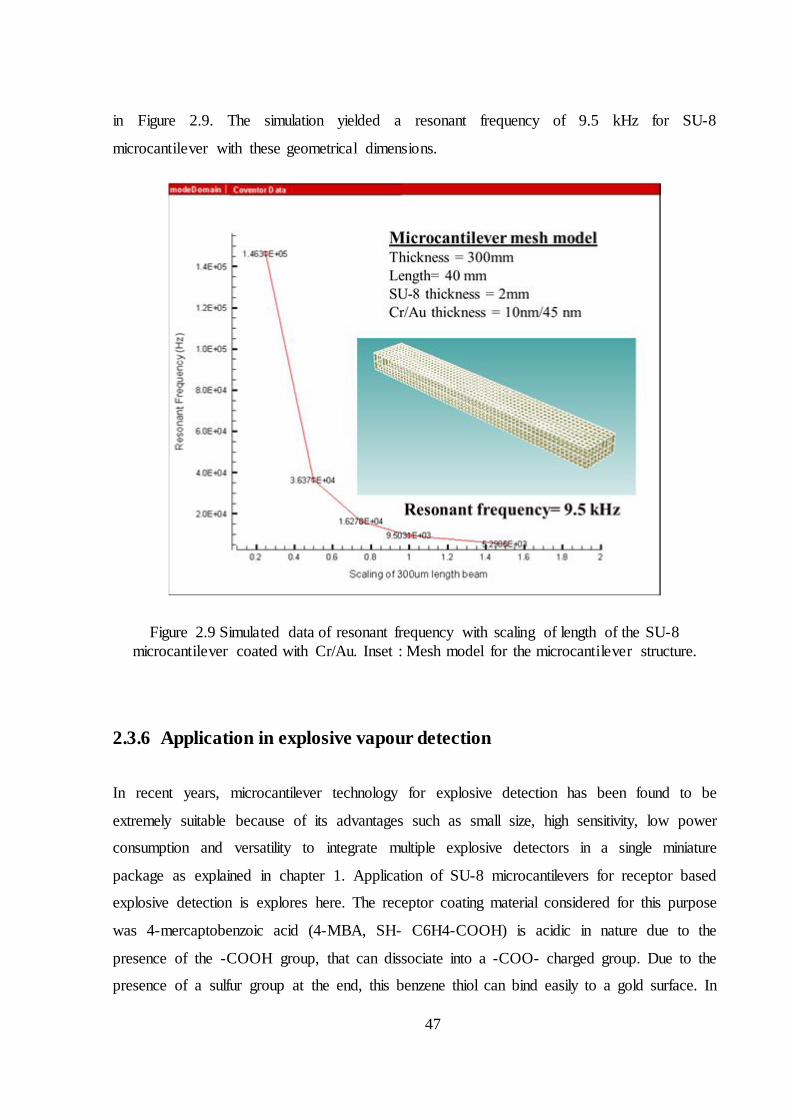
47
in Figure 2.9. The simulation yielded a resonant frequency of 9.5 kHz for SU-8
microcantilever with these geometrical dimensions.
Figure 2.9 Simulated data of resonant frequency with scaling of length of the SU-8 microcantilever coated with Cr/Au. Inset : Mesh model for the microcantilever structure.
2.3.6 Application in explosive vapour detection
In recent years, microcantilever technology for explosive detection has been found to be
extremely suitable because of its advantages such as small size, high sensitivity, low power
consumption and versatility to integrate multiple explosive detectors in a single miniature
package as explained in chapter 1. Application of SU-8 microcantilevers for receptor based
explosive detection is explores here. The receptor coating material considered for this purpose
was 4-mercaptobenzoic acid (4-MBA, SH- C6H4-COOH) is acidic in nature due to the
presence of the -COOH group, that can dissociate into a -COO- charged group. Due to the
presence of a sulfur group at the end, this benzene thiol can bind easily to a gold surface. In
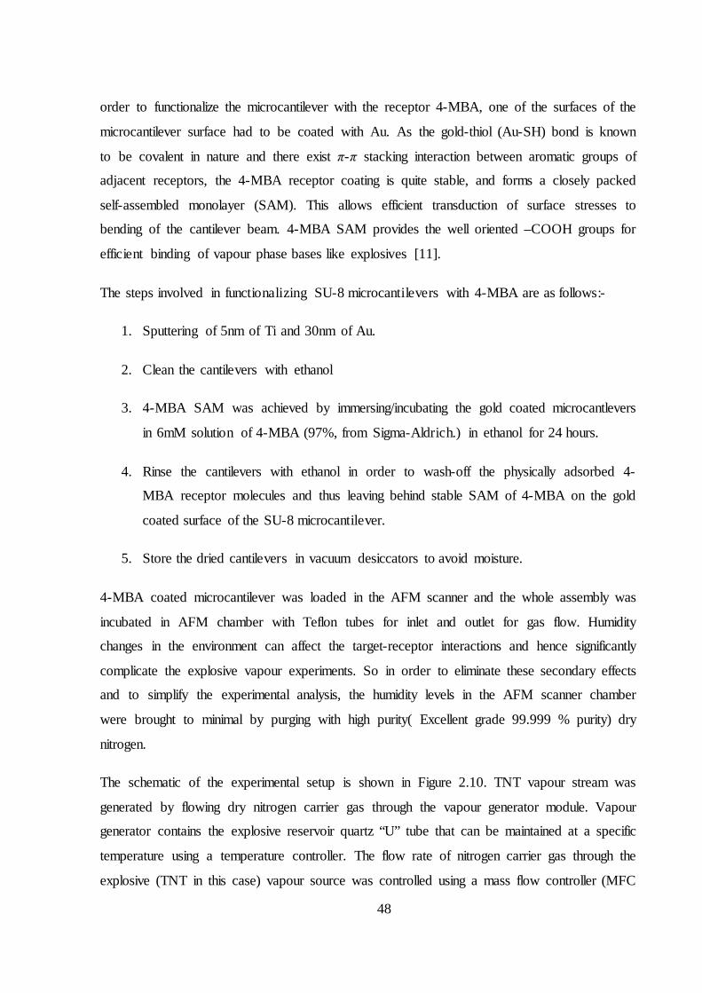
48
order to functionalize the microcantilever with the receptor 4-MBA, one of the surfaces of the
microcantilever surface had to be coated with Au. As the gold-thiol (Au-SH) bond is known
to be covalent in nature and there exist π-π stacking interaction between aromatic groups of
adjacent receptors, the 4-MBA receptor coating is quite stable, and forms a closely packed
self-assembled monolayer (SAM). This allows efficient transduction of surface stresses to
bending of the cantilever beam. 4-MBA SAM provides the well oriented –COOH groups for
efficient binding of vapour phase bases like explosives [11].
The steps involved in functionalizing SU-8 microcantilevers with 4-MBA are as follows:-
1. Sputtering of 5nm of Ti and 30nm of Au.
2. Clean the cantilevers with ethanol
3. 4-MBA SAM was achieved by immersing/incubating the gold coated microcantlevers
in 6mM solution of 4-MBA (97%, from Sigma-Aldrich.) in ethanol for 24 hours.
4. Rinse the cantilevers with ethanol in order to wash-off the physically adsorbed 4-
MBA receptor molecules and thus leaving behind stable SAM of 4-MBA on the gold
coated surface of the SU-8 microcantilever.
5. Store the dried cantilevers in vacuum desiccators to avoid moisture.
4-MBA coated microcantilever was loaded in the AFM scanner and the whole assembly was
incubated in AFM chamber with Teflon tubes for inlet and outlet for gas flow. Humidity
changes in the environment can affect the target-receptor interactions and hence significantly
complicate the explosive vapour experiments. So in order to eliminate these secondary effects
and to simplify the experimental analysis, the humidity levels in the AFM scanner chamber
were brought to minimal by purging with high purity( Excellent grade 99.999 % purity) dry
nitrogen.
The schematic of the experimental setup is shown in Figure 2.10. TNT vapour stream was
generated by flowing dry nitrogen carrier gas through the vapour generator module. Vapour
generator contains the explosive reservoir quartz “U” tube that can be maintained at a specific
temperature using a temperature controller. The flow rate of nitrogen carrier gas through the
explosive (TNT in this case) vapour source was controlled using a mass flow controller (MFC
49
from SIERRA). The gas flow rate was maintained at 30 SCCM (Standard Cubic Centimetre
per Minute) using the MFC. When the TNT vapour stream had to be stopped, the same carrier
gas flow was maintained through the microcantilever gas flow cell by redirecting the nitrogen
flow stream through a bypass line. This switching between TNT vapour stream and dry
nitrogen stream was performed using three way valves V1 and V2.
Initial experiments were carried out with TNT vapour generated at 65oC. AFM chamber was
purged with dry nitrogen till the signal got stabilized. Purging was done for 1-2 hours before
starting the experiment. This helped in reducing the humidity levels. The response of the
microcantilever for TNT vapour is shown in Figure 2.11.
Figure 2.10 Experimental setup for explosive vapour experiment (A) Schematic of the setup
(B) Explosive vapour generator

50
Figure 2.11 Response of the microcantilever to TNT vapour stream generated at 65oC with a
flow rate of 30 SCCM
The microcantilever response curve verifies the proof of concept of detection of TNT vapours
using 4-MBA coated SU-8 microcantilevers. The response curve indicates the direction of
bending of the microcantilever the side in which laser is focussed which is the gold coated
surface. Curvature of the microcantilever in this direction could indicate presence of
compressive stress in the gold coating. This experimental result could be supported by the
theoretical analysis for the interaction chemistry between 4-MBA and a similar molecule,
dinitrotoluene (DNT) which is a decomposition product of TNT [97] which is also a
nitroaromatic with two nitro groups. The origin of compressive stress could be either of the
two possible interactions given below:-
1. Considering the case of closely packed 4-MBA SAM without any defect. The TNT
molecule can bring the adjacent thiol molecules of the 4-MBA SAM closer to each other
via hydrogen bonding. This leads to a compressive stress in the gold film (Figure 2.12(B).
2. Considering the case of microcantilever functionalized with 4-MBA SAM with certain
defects leading to grain boundaries in the SAM. In this case the TNT molecule can
occupy the grain boundaries and generate attractive forces between adjascent receptor
molecules via weak pi-pi interactions and hydrogen bonding. This can also lead to
compressive stress in the gold film (Figure 2.12(C)).
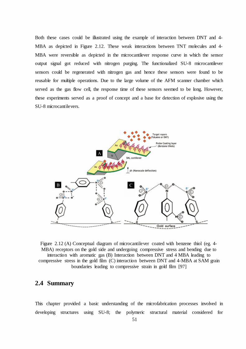
51
Both these cases could be illustrated using the example of interaction between DNT and 4-
MBA as depicted in Figure 2.12. These weak interactions between TNT molecules and 4-
MBA were reversible as depicted in the microcantilever response curve in which the sensor
output signal got reduced with nitrogen purging. The functionalized SU-8 microcantilever
sensors could be regenerated with nitrogen gas and hence these sensors were found to be
reusable for multiple operations. Due to the large volume of the AFM scanner chamber which
served as the gas flow cell, the response time of these sensors seemed to be long. However,
these experiments served as a proof of concept and a base for detection of explosive using the
SU-8 microcantilevers.
Figure 2.12 (A) Conceptual diagram of microcantilever coated with benzene thiol (eg. 4-MBA) receptors on the gold side and undergoing compressive stress and bending due to
interaction with aromatic gas (B) Interaction between DNT and 4 MBA leading to compressive stress in the gold film (C) interaction between DNT and 4-MBA at SAM grain
boundaries leading to compressive strain in gold film [97]
2.4 Summary
This chapter provided a basic understanding of the microfabrication processes involved in
developing structures using SU-8; the polymeric structural material considered for
52
microcantilevers. A simple fully polymeric microcantilever sensor device with a single layer
of SU-8 in the microcantilever structure with a capability to optically detect surface stress of
few mN/m was designed and fabricated. The process followed allowed the fabrication of all
polymer structures on a dummy substrate and release of the structures from the substrate by
removing the sacrificial layer. The capabilities of thin films of HSQ and sputtered silicon
dioxide as sacrificial layers were explored and were found to be better candidates compared to
the release layers reported in the literature. The unit processes in fabricating single layer SU-8
microcantilevers were optimized and this could serve as a base work for fabrication of
multilayer SU-8 microcantilevers that has been developed in the lab as part of this thesis
work. The fabricated SU-8 microcantilevers for optical transduction were characterized using
standard AFM. An application for these microcantilevers for detection of explosive vapours,
TNT has been successfully implemented. The functionalization protocol and the explosive
vapour experiments could also serve as a background work in developing sensors for
explosive detection using SU-8 microcantilever with integrated electrical transduction
mechanism to be discussed in chapter 4.
53
Chapter 3
Polymer Nanocomposite Microcantilever Sensor with
Integrated Electrical Transduction
3.1 Introduction
Microcantilevers with integrated piezoresistors perform electrical transduction of strain by
resultant change in resistance. Therefore, when a microcantilever with its surface
functionalised with a coating that is selective to target molecules is exposed to the analyte, the
molecular adsorption induces a differential surface stress between top and bottom surface of
the microcantilevers. This differential surface stress results in a change in resistance of the
piezoresistive layer as represented in equation1.8 in Chapter 1, which says that surface stress
sensitivity depends on the ratio of gauge factor (K) of the piezoresistive film to the Young’s
modulus (E) of the structural material. The development of SU-8 (low Young’s modulus)
microcantilever with SU-8 nanocomposite piezoresistor (aimed at providing good gauge
factor and low young’s modulus) is presented in this chapter. Added to the benefit of expected
improvement in sensitivity, unlike the previously reported piezoresistive layers used in SU-8
54
microcantilevers, SU-8 nanocomposite piezoresistor would exhibit compliance compatibility
with that of the structural material, SU-8.
The device concept of a polymer nanocomposite microcantilever is to embed a piezoresistive
nanocomposite made of SU-8 and Carbon Black (CB) conducting nanoparticles inside an SU-
8 microcantilever. A similar idea was reported in [57] in which SU-8 microcantilevers of
thickness 7 m with embedded SU-8/CB nanocomposite (16 wt. % of CB in SU-8)
piezoresistor with a gauge factor in the range of 15-20 was presented. However further
improvements in device or process development or detailed characterization of the device for
evaluating and optimizing the performances of these polymer devices for any kind of sensing
applications have not been reported. There is still a lot of room for improvement in this
technology and developing a platform based on this technology for many applications in
bio/chemical sensing.
The performance of SU-8 nanocomposite microcantilevers could be improved on first hand
by improving the dispersion of CB in SU-8 and reducing the thickness of the cantilever
structure which is discussed in this chapter. The other focus points discussed in this chapter
pertain to the improvement in performance of polymer nanocomposite microcantilever
sensors that could be achieved by (i) performing a systematic characterization of the SU-8/CB
nanocomposite in order to understand its electrical and mechanical characteristics. This was
required to decide the optimal range of concentration of CB filler in SU-8 in order to improve
the overall performance of the polymer nanocomposite microcantilever sensors in terms of
sensitivity and device variability. (ii) Improving the microcantilever design aimed for surface
stress measurement based nanomechanical cantilever. (iii) Systematic characterization of the
fabricated microcantilever devices for analysing their electrical, mechanical,
electromechanical and noise characteristics. These analyses are of prime importance in
verifying the capability of these polymer nanocomposite microcantilevers for bio/chemical
sensing applications.
3.2 SU-8/CB nanocomposite thin film preparation and patterning
The polymer nanocomposite was prepared by ultrasonic mixing of a high-structured Carbon
Black (CB), Conductex 7067 Ultra (Columbian Chemicals) in SU-8 and Nanothinner
55
(Microchem). The diameter of carbon black nanoparticles was approximately 40 nm. In order
to use SU-8/Carbon black as piezoresistor layer, the composite material should satisfy certain
prerequisites such as (i) possess proper dispersion of CB in SU-8 (ii) it should be spin
coatable and photo-lithographically patternable with compatible process close to that of SU-8
(iii) it should be conductive and piezoresistive (v) possess thermal and mechanical stability
similar to SU-8 (vi) possess compliance compatibility with SU-8 (similar Young’ modulus
value as that of SU-8). SU-8/CB nanocomposites were prepared and characterized in order to
investigate in these aspects.
The preparation of SU-8/CB nanocomposite layer involves the following steps:-
1. Carbon Black being hygroscopic, it was required to pre-heat the CB powder in a baking
oven at a temperature between 100oC and 110oC to remove the trapped moisture.
2. Mechanically grind the CB powder and weigh the quantity as per the required
concentration of CB in SU-8 typically quantified as CB weight percentage or CB volume
percentage. CB weight % and CB volume % can be defined as
퐶퐵푤푒푖푔ℎ푡% =
(푀 )(푀 ) + 푉 × 휌
× 100 (3.1)
퐶퐵푉표푙푢푚푒% =
⎩⎪⎨
⎪⎧ 푀
휌
푀휌 + 푉
⎭⎪⎬
⎪⎫
× 100 (3.2)
Where M,휌 and V are mass, density and volume respectively. 휌 = 1.12 g/mL ;
휌 =1.2 g/mL
3. Ultrasonic mixing process of CB in SU-8.
The mixing processes of CB in SU-8 2002 were tried out with bath ultra-sonication as
well as probe sonication out of which the probe sonication provided better dispersion than
the other. Sonication was carried out at energy of 600 J. Sonication generated lot of heat
because of which the solvent in the SU-8 was found to get evaporated, leaving a highly
viscous SU-8 /CB mixtures which were very difficult to be spin coated. This problem was
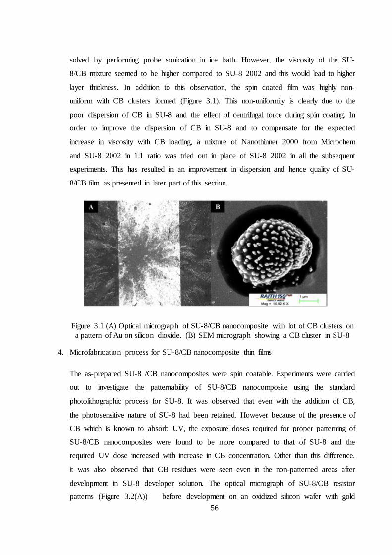
56
solved by performing probe sonication in ice bath. However, the viscosity of the SU-
8/CB mixture seemed to be higher compared to SU-8 2002 and this would lead to higher
layer thickness. In addition to this observation, the spin coated film was highly non-
uniform with CB clusters formed (Figure 3.1). This non-uniformity is clearly due to the
poor dispersion of CB in SU-8 and the effect of centrifugal force during spin coating. In
order to improve the dispersion of CB in SU-8 and to compensate for the expected
increase in viscosity with CB loading, a mixture of Nanothinner 2000 from Microchem
and SU-8 2002 in 1:1 ratio was tried out in place of SU-8 2002 in all the subsequent
experiments. This has resulted in an improvement in dispersion and hence quality of SU-
8/CB film as presented in later part of this section.
Figure 3.1 (A) Optical micrograph of SU-8/CB nanocomposite with lot of CB clusters on a pattern of Au on silicon dioxide. (B) SEM micrograph showing a CB cluster in SU-8
4. Microfabrication process for SU-8/CB nanocomposite thin films
The as-prepared SU-8 /CB nanocomposites were spin coatable. Experiments were carried
out to investigate the patternability of SU-8/CB nanocomposite using the standard
photolithographic process for SU-8. It was observed that even with the addition of CB,
the photosensitive nature of SU-8 had been retained. However because of the presence of
CB which is known to absorb UV, the exposure doses required for proper patterning of
SU-8/CB nanocomposites were found to be more compared to that of SU-8 and the
required UV dose increased with increase in CB concentration. Other than this difference,
it was also observed that CB residues were seen even in the non-patterned areas after
development in SU-8 developer solution. The optical micrograph of SU-8/CB resistor
patterns (Figure 3.2(A)) before development on an oxidized silicon wafer with gold
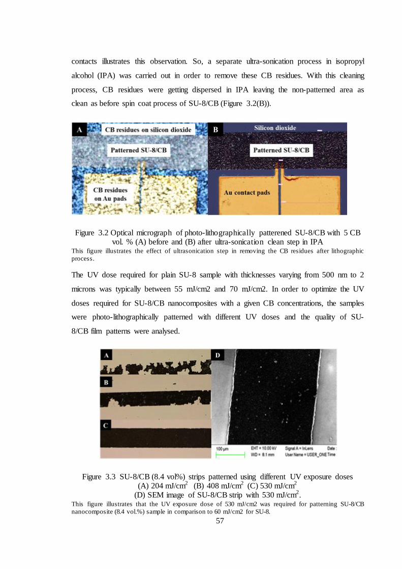
57
contacts illustrates this observation. So, a separate ultra-sonication process in isopropyl
alcohol (IPA) was carried out in order to remove these CB residues. With this cleaning
process, CB residues were getting dispersed in IPA leaving the non-patterned area as
clean as before spin coat process of SU-8/CB (Figure 3.2(B)).
Figure 3.2 Optical micrograph of photo-lithographically patterened SU-8/CB with 5 CB vol. % (A) before and (B) after ultra-sonication clean step in IPA
This figure illustrates the effect of ultrasonication step in removing the CB residues after lithographic process.
The UV dose required for plain SU-8 sample with thicknesses varying from 500 nm to 2
microns was typically between 55 mJ/cm2 and 70 mJ/cm2. In order to optimize the UV
doses required for SU-8/CB nanocomposites with a given CB concentrations, the samples
were photo-lithographically patterned with different UV doses and the quality of SU-
8/CB film patterns were analysed.
Figure 3.3 SU-8/CB (8.4 vol%) strips patterned using different UV exposure doses (A) 204 mJ/cm2 (B) 408 mJ/cm2 (C) 530 mJ/cm2
(D) SEM image of SU-8/CB strip with 530 mJ/cm2. This figure illustrates that the UV exposure dose of 530 mJ/cm2 was required for patterning SU-8/CB nanocomposite (8.4 vol.%) sample in comparison to 60 mJ/cm2 for SU-8.
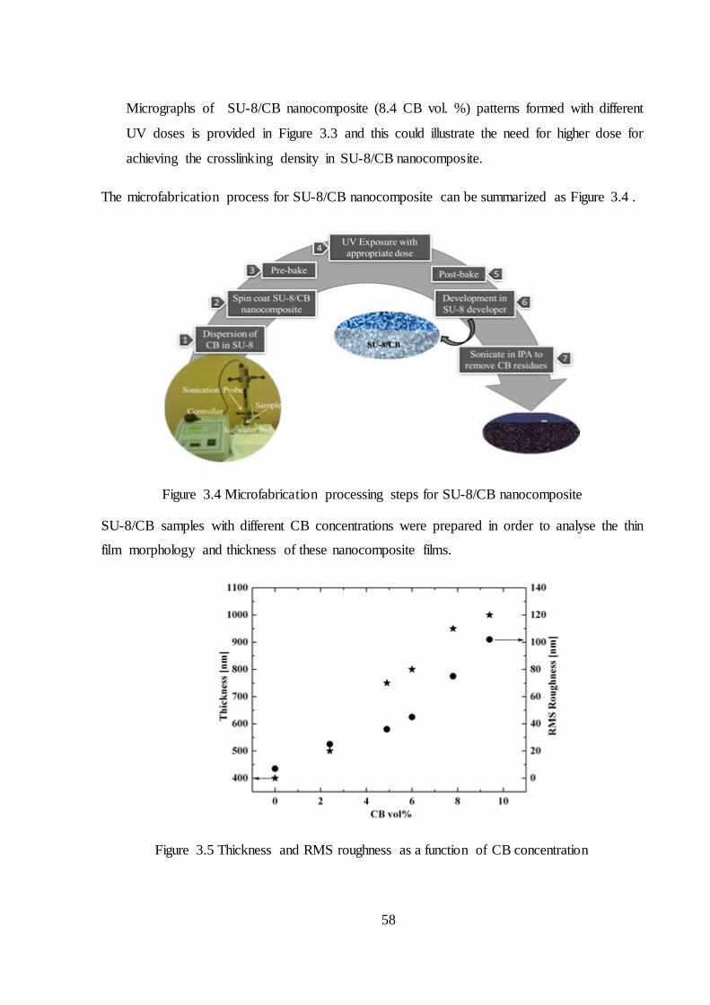
58
Micrographs of SU-8/CB nanocomposite (8.4 CB vol. %) patterns formed with different
UV doses is provided in Figure 3.3 and this could illustrate the need for higher dose for
achieving the crosslinking density in SU-8/CB nanocomposite.
The microfabrication process for SU-8/CB nanocomposite can be summarized as Figure 3.4 .
Figure 3.4 Microfabrication processing steps for SU-8/CB nanocomposite
SU-8/CB samples with different CB concentrations were prepared in order to analyse the thin
film morphology and thickness of these nanocomposite films.
Figure 3.5 Thickness and RMS roughness as a function of CB concentration
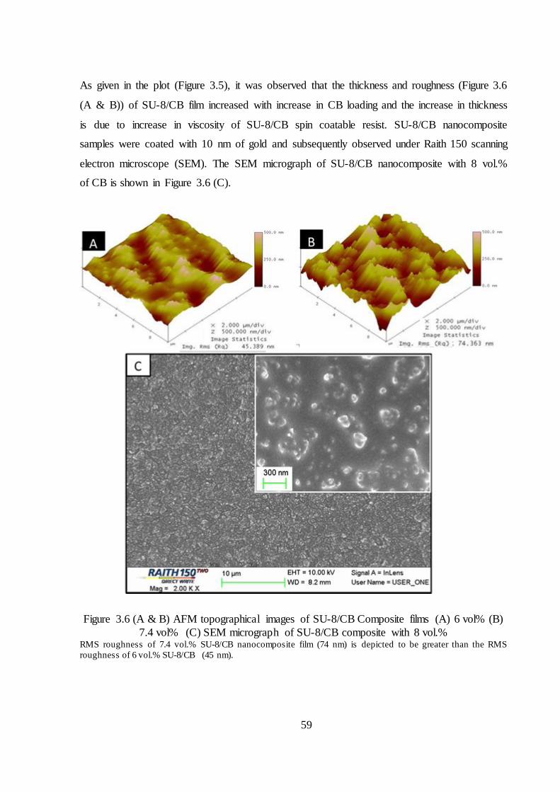
59
As given in the plot (Figure 3.5), it was observed that the thickness and roughness (Figure 3.6
(A & B)) of SU-8/CB film increased with increase in CB loading and the increase in thickness
is due to increase in viscosity of SU-8/CB spin coatable resist. SU-8/CB nanocomposite
samples were coated with 10 nm of gold and subsequently observed under Raith 150 scanning
electron microscope (SEM). The SEM micrograph of SU-8/CB nanocomposite with 8 vol.%
of CB is shown in Figure 3.6 (C).
Figure 3.6 (A & B) AFM topographical images of SU-8/CB Composite films (A) 6 vol% (B) 7.4 vol% (C) SEM micrograph of SU-8/CB composite with 8 vol.%
RMS roughness of 7.4 vol.% SU-8/CB nanocomposite film (74 nm) is depicted to be greater than the RMS roughness of 6 vol.% SU-8/CB (45 nm).
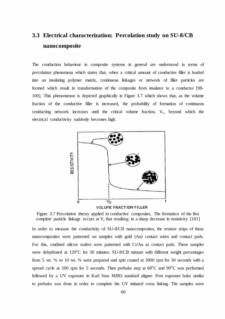
60
3.3 Electrical characterization: Percolation study on SU-8/CB
nanocomposite
The conduction behaviour in composite systems in general are understood in terms of
percolation phenomena which states that, when a critical amount of conductive filler is loaded
into an insulating polymer matrix, continuous linkages or network of filler particles are
formed which result in transformation of the composite from insulator to a conductor [98-
100]. This phenomenon is depicted graphically in Figure 3.7 which shows that, as the volume
fraction of the conductive filler is increased, the probability of formation of continuous
conducting network increases until the critical volume fraction, Vc, beyond which the
electrical conductivity suddenly becomes high.
Figure 3.7 Percolation theory applied to conductive composites. The formation of the first complete particle linkage occurs at Vc that resulting in a sharp decrease in resistivity [101]
In order to measure the conductivity of SU-8/CB nanocomposites, the resistor strips of these
nanocomposites were patterned on samples with gold (Au) contact wires and contact pads.
For this, oxidized silicon wafers were patterned with Cr/Au as contact pads. These samples
were dehydrated at 120oC for 30 minutes. SU-8/CB mixture with different weight percentages
from 5 wt. % to 10 wt. % were prepared and spin coated at 3000 rpm for 30 seconds with a
spread cycle at 500 rpm for 5 seconds. Then prebake step at 68oC and 90oC was performed
followed by a UV exposure in Karl Suss MJB3 standard aligner. Post exposure bake similar
to prebake was done in order to complete the UV initiated cross linking. The samples were

61
developed in SU-8 developer and finally ultrasonicated in IPA leaving SU-8/CB strip patterns
between the Au electrodes (Figure 3.2(B)).
Figure 3.8 Percolation characteristics of SU-8/CB composite. Power law fit parameters indicate a good fit with R2 = 0.99 and percolation threshold, fc = 6.5 wt.% ( or 6.1 vol.%)
The resistors were probed inside standard Suss Microtech probe station and their resistances
were measured using Keithley 2602 source measuring unit. The resistivity of these composite
resistors decreased with increase in CB wt. % (Figure 3.8). This obeyed a power law equation
for percolation, given by resistivity, ρ ~ (f - fc)-t where f is the fraction of the conductive filler
and fc is the critical fraction known as the percolation threshold and t is the critical exponent
[102]. This power law fit on the experimental data yielded a typical percolation threshold of
6.5 wt%. The conduction in these films was due to the formation of carbon black conductive
network which became denser with increase in conductive particle concentration as depicted
in Figure 3.9.
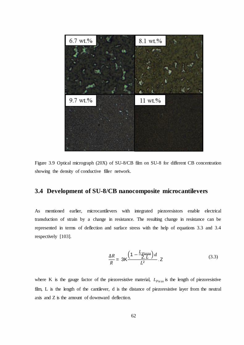
62
Figure 3.9 Optical micrograph (20X) of SU-8/CB film on SU-8 for different CB concentration
showing the density of conductive filler network.
3.4 Development of SU-8/CB nanocomposite microcantilevers
As mentioned earlier, microcantilevers with integrated piezoresistors enable electrical
transduction of strain by a change in resistance. The resulting change in resistance can be
represented in terms of deflection and surface stress with the help of equations 3.3 and 3.4
respectively [103].
∆푅푅
= 3K1 −퐿
2. 퐿 푑
퐿. Z (3.3)
where K is the gauge factor of the piezoresistive material, Pie zoL is the length of piezoresistive
film, L is the length of the cantilever, d is the distance of piezoresistive layer from the neutral
axis and Z is the amount of downward deflection.
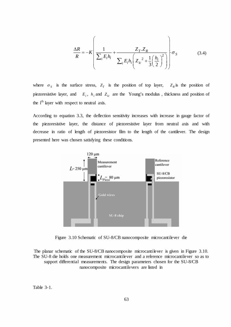
63
22
1 .
13 2
T RS
i ii ii i ici
R Z ZKR E h hE h Z
(3.4)
where S is the surface stress, TZ is the position of top layer, RZ is the position of
piezoresistive layer, and iE , ih and icZ are the Young’s modulus , thickness and position of
the ith layer with respect to neutral axis.
According to equation 3.3, the deflection sensitivity increases with increase in gauge factor of
the piezoresistive layer, the distance of piezoresistive layer from neutral axis and with
decrease in ratio of length of piezoresistor film to the length of the cantilever. The design
presented here was chosen satisfying these conditions.
Figure 3.10 Schematic of SU-8/CB nanocomposite microcantilever die
The planar schematic of the SU-8/CB nanocomposite microcantilever is given in Figure 3.10. The SU-8 die holds one measurement microcantilever and a reference microcantilever so as to
support differential measurements. The design parameters chosen for the SU-8/CB nanocomposite microcantilevers are listed in
Table 3-1.
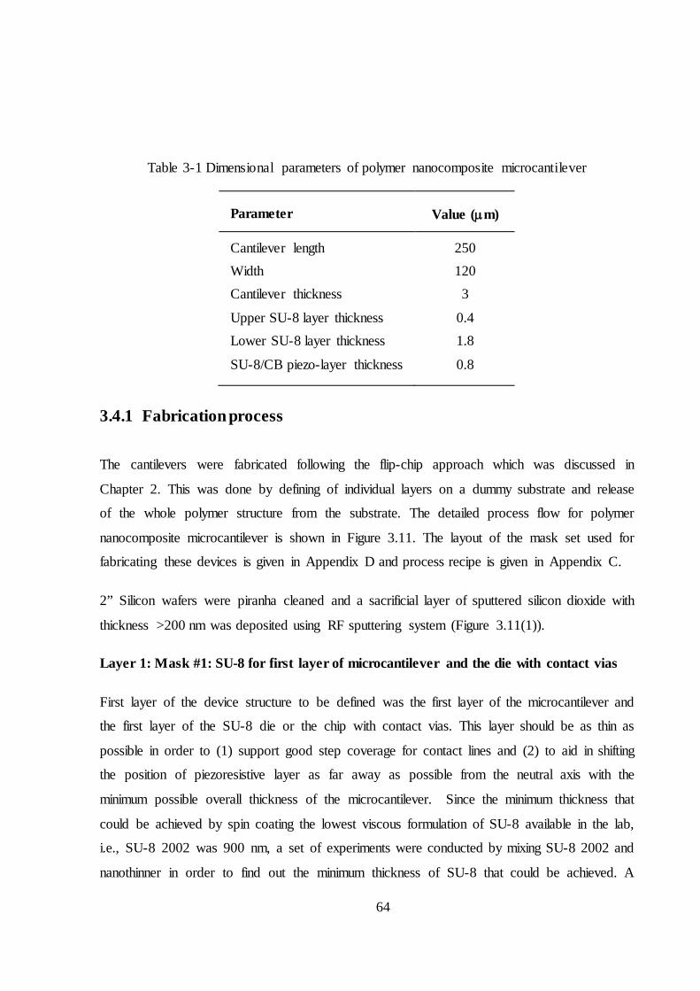
64
Table 3-1 Dimensional parameters of polymer nanocomposite microcantilever
Parameter Value (m)
Cantilever length 250 Width 120 Cantilever thickness 3
Upper SU-8 layer thickness 0.4 Lower SU-8 layer thickness 1.8
SU-8/CB piezo-layer thickness 0.8
3.4.1 Fabrication process
The cantilevers were fabricated following the flip-chip approach which was discussed in
Chapter 2. This was done by defining of individual layers on a dummy substrate and release
of the whole polymer structure from the substrate. The detailed process flow for polymer
nanocomposite microcantilever is shown in Figure 3.11. The layout of the mask set used for
fabricating these devices is given in Appendix D and process recipe is given in Appendix C.
2” Silicon wafers were piranha cleaned and a sacrificial layer of sputtered silicon dioxide with
thickness >200 nm was deposited using RF sputtering system (Figure 3.11(1)).
Layer 1: Mask #1: SU-8 for first layer of microcantilever and the die with contact vias
First layer of the device structure to be defined was the first layer of the microcantilever and
the first layer of the SU-8 die or the chip with contact vias. This layer should be as thin as
possible in order to (1) support good step coverage for contact lines and (2) to aid in shifting
the position of piezoresistive layer as far away as possible from the neutral axis with the
minimum possible overall thickness of the microcantilever. Since the minimum thickness that
could be achieved by spin coating the lowest viscous formulation of SU-8 available in the lab,
i.e., SU-8 2002 was 900 nm, a set of experiments were conducted by mixing SU-8 2002 and
nanothinner in order to find out the minimum thickness of SU-8 that could be achieved. A
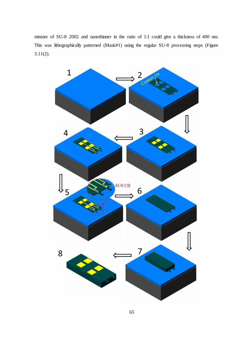
65
mixture of SU-8 2002 and nanothinner in the ratio of 1:1 could give a thickness of 400 nm.
This was lithographically patterned (Mask#1) using the regular SU-8 processing steps (Figure
3.11(2).
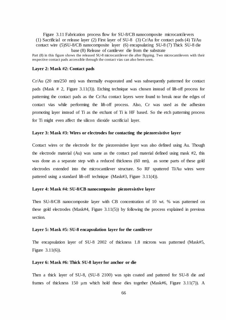
66
Figure 3.11 Fabrication process flow for SU-8/CB nanocomposite microcantilevers (1) Sacrificial or release layer (2) First layer of SU-8 (3) Cr/Au for contact pads (4) Ti/Au contact wire (5)SU-8/CB nanocomposite layer (6) encapsulating SU-8 (7) Thick SU-8 die
base (8) Release of cantilever die from the substrate Part (8) in this figure shows the released SU-8 microcantilever die after flipping. Two microcantilevers with their respective contact pads accessible through the contact vias can also been seen.
Layer 2: Mask #2: Contact pads
Cr/Au (20 nm/250 nm) was thermally evaporated and was subsequently patterned for contact
pads (Mask # 2, Figure 3.11(3)). Etching technique was chosen instead of lift-off process for
patterning the contact pads as the Cr/Au contact layers were found to break near the edges of
contact vias while performing the lift-off process. Also, Cr was used as the adhesion
promoting layer instead of Ti as the etchant of Ti is HF based. So the etch patterning process
for Ti might even affect the silicon dioxide sacrificial layer.
Layer 3: Mask #3: Wires or electrodes for contacting the piezoresistive layer
Contact wires or the electrode for the piezoresistive layer was also defined using Au. Though
the electrode material (Au) was same as the contact pad material defined using mask #2, this
was done as a separate step with a reduced thickness (60 nm), as some parts of these gold
electrodes extended into the microcantilever structure. So RF sputtered Ti/Au wires were
pattered using a standard lift-off technique (Mask#3, Figure 3.11(4)).
Layer 4: Mask #4: SU-8/CB nanocomposite piezoresistive layer
Then SU-8/CB nanocomposite layer with CB concentration of 10 wt. % was patterned on
these gold electrodes (Mask#4, Figure 3.11(5)) by following the process explained in previous
section.
Layer 5: Mask #5: SU-8 encapsulation layer for the cantilever
The encapsulation layer of SU-8 2002 of thickness 1.8 microns was patterned (Mask#5,
Figure 3.11(6)).
Layer 6: Mask #6: Thick SU-8 layer for anchor or die
Then a thick layer of SU-8, (SU-8 2100) was spin coated and pattered for SU-8 die and
frames of thickness 150 m which hold these dies together (Mask#6, Figure 3.11(7)). A
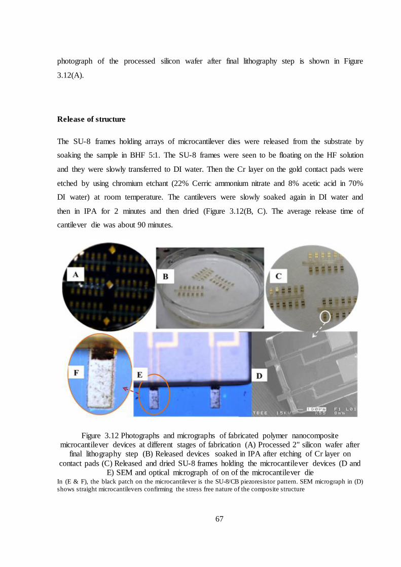
67
photograph of the processed silicon wafer after final lithography step is shown in Figure
3.12(A).
Release of structure
The SU-8 frames holding arrays of microcantilever dies were released from the substrate by
soaking the sample in BHF 5:1. The SU-8 frames were seen to be floating on the HF solution
and they were slowly transferred to DI water. Then the Cr layer on the gold contact pads were
etched by using chromium etchant (22% Cerric ammonium nitrate and 8% acetic acid in 70%
DI water) at room temperature. The cantilevers were slowly soaked again in DI water and
then in IPA for 2 minutes and then dried (Figure 3.12(B, C). The average release time of
cantilever die was about 90 minutes.
Figure 3.12 Photographs and micrographs of fabricated polymer nanocomposite microcantilever devices at different stages of fabrication (A) Processed 2" silicon wafer after
final lithography step (B) Released devices soaked in IPA after etching of Cr layer on contact pads (C) Released and dried SU-8 frames holding the microcantilever devices (D and
E) SEM and optical micrograph of on of the microcantilever die In (E & F), the black patch on the microcantilever is the SU-8/CB piezoresistor pattern. SEM micrograph in (D) shows straight microcantilevers confirming the stress free nature of the composite structure
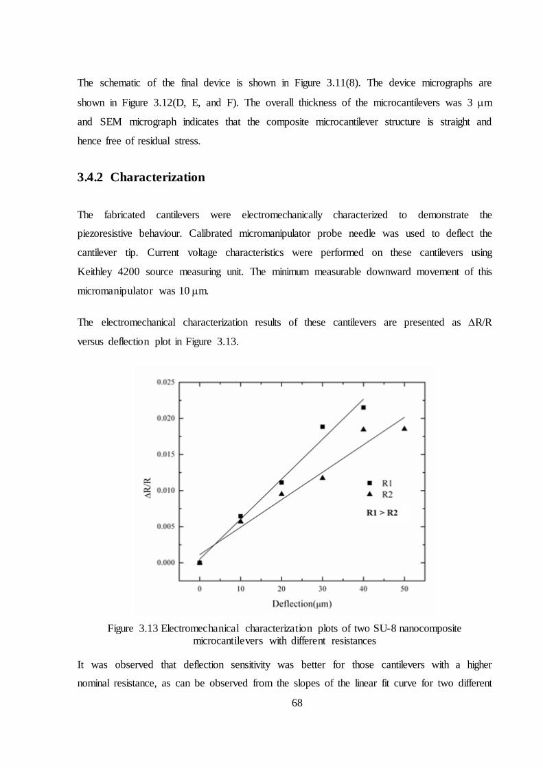
68
The schematic of the final device is shown in Figure 3.11(8). The device micrographs are
shown in Figure 3.12(D, E, and F). The overall thickness of the microcantilevers was 3 m
and SEM micrograph indicates that the composite microcantilever structure is straight and
hence free of residual stress.
3.4.2 Characterization
The fabricated cantilevers were electromechanically characterized to demonstrate the
piezoresistive behaviour. Calibrated micromanipulator probe needle was used to deflect the
cantilever tip. Current voltage characteristics were performed on these cantilevers using
Keithley 4200 source measuring unit. The minimum measurable downward movement of this
micromanipulator was 10 m.
The electromechanical characterization results of these cantilevers are presented as R/R
versus deflection plot in Figure 3.13.
Figure 3.13 Electromechanical characterization plots of two SU-8 nanocomposite
microcantilevers with different resistances
It was observed that deflection sensitivity was better for those cantilevers with a higher
nominal resistance, as can be observed from the slopes of the linear fit curve for two different
69
samples of varying resistances. The highest deflection sensitivity achieved with these devices
was 0.55 ppm/nm. Using this experimental result on deflection sensitivity, the gauge factor of
the 10 wt. % SU-8/CB nanocomposite piezoresistor was extracted using equation 3.3. The
gauge factor was found to be 20 that is approximately 10 times higher compared to Au strain
gauges. The surface stress sensitivity of these cantilevers was extracted using equation 3.4 and
was found to be 4.1x10⁻³ [N/m]-1. This is 10 times the sensitivity of the SU-8 cantilever with
Au [34] and at least a factor of two higher compared to the previously reported results on SU-
8/CB composite cantilevers [57] . This could be attributed primarily to the lower thicknesses
of the piezoresistive layer and the microcantilever structure achieved with this fabrication
process.
3.4.3 Shortcomings and scope for improvement
(i) The fabricated devices exhibited good deflection sensitivity and surface stress
sensitivity. The design helped in investigating the feasibility of fabricating polymer
nanocomposite microcantilevers with a minimum thickness of 3 m and aided in
extracting the gauge factor of SU-8/CB nanocomposite. However, the design of the
device is not optimum for surface stress measurements based microcantilevers for
bio/chemical sensors, as the SU-8/CB nanocomposite piezoresistive layer did not
encompass the entire length of the cantilever.
(ii) Process and device variability due to statistical distribution of CB in SU-8 matrix
and edge roughness and random breakages of SU-8/CB pattern formed during the
final ultra-sonication cleaning step. A systematic characterization experiment to
study the dispersion of CB in SU-8 was required in order to understand the source of
variability and to optimize the SU-8/CB nanocomposite preparation process.
(iii) Though the sensor concept with improved sensitivity was demonstrated, a systematic
characterization study of the SU-8/CB nanocomposite was necessary to decide the
optimal range of concentration of CB filler in SU-8.
(iv) The fabrication process was complex with 6 levels of lithography which obviously
affect the process yield and increases the cost of fabrication. So the possibility of
reducing the number of mask levels had to be investigated.
(v) Sensitivity of the SU-8/CB nanocomposite sensor was as high as 4 ppm [mN/m]-1.
But in order to evaluate the sensor for any application, along with the
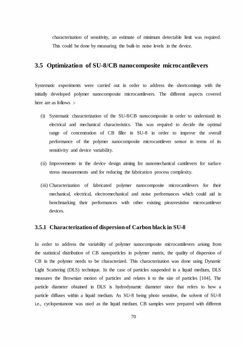
70
characterization of sensitivity, an estimate of minimum detectable limit was required.
This could be done by measuring the built-in noise levels in the device.
3.5 Optimization of SU-8/CB nanocomposite microcantilevers
Systematic experiments were carried out in order to address the shortcomings with the
initially developed polymer nanocomposite microcantilevers. The different aspects covered
here are as follows :-
(i) Systematic characterization of the SU-8/CB nanocomposite in order to understand its
electrical and mechanical characteristics. This was required to decide the optimal
range of concentration of CB filler in SU-8 in order to improve the overall
performance of the polymer nanocomposite microcantilever sensor in terms of its
sensitivity and device variability.
(ii) Improvements in the device design aiming for nanomechanical cantilevers for surface
stress measurements and for reducing the fabrication process complexity.
(iii) Characterization of fabricated polymer nanocomposite microcantilevers for their
mechanical, electrical, electromechanical and noise performances which could aid in
benchmarking their performances with other existing piezoresistive microcantilever
devices.
3.5.1 Characterization of dispersion of Carbon black in SU-8
In order to address the variability of polymer nanocomposite microcantilevers arising from
the statistical distribution of CB nanoparticles in polymer matrix, the quality of dispersion of
CB in the polymer needs to be characterized. This characterization was done using Dynamic
Light Scattering (DLS) technique. In the case of particles suspended in a liquid medium, DLS
measures the Brownian motion of particles and relates it to the size of particles [104]. The
particle diameter obtained in DLS is hydrodynamic diameter since that refers to how a
particle diffuses within a liquid medium. As SU-8 being photo sensitive, the solvent of SU-8
i.e., cyclopentanone was used as the liquid medium. CB samples were prepared with different
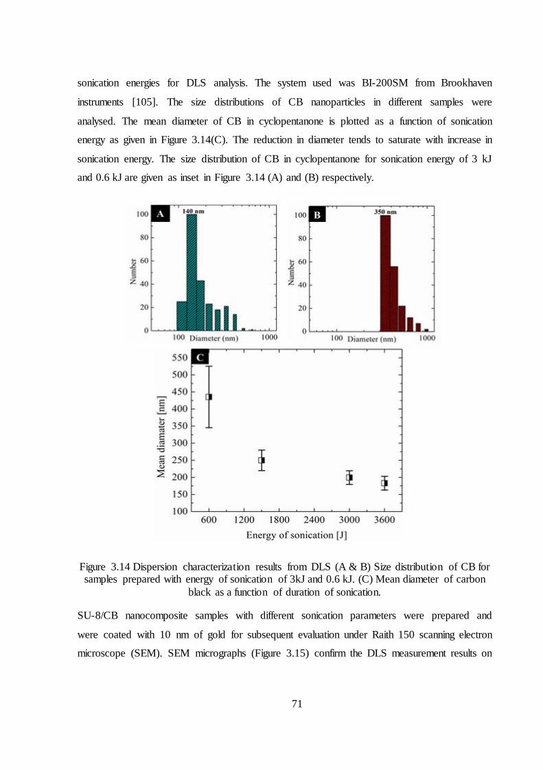
71
sonication energies for DLS analysis. The system used was BI-200SM from Brookhaven
instruments [105]. The size distributions of CB nanoparticles in different samples were
analysed. The mean diameter of CB in cyclopentanone is plotted as a function of sonication
energy as given in Figure 3.14(C). The reduction in diameter tends to saturate with increase in
sonication energy. The size distribution of CB in cyclopentanone for sonication energy of 3 kJ
and 0.6 kJ are given as inset in Figure 3.14 (A) and (B) respectively.
Figure 3.14 Dispersion characterization results from DLS (A & B) Size distribution of CB for samples prepared with energy of sonication of 3kJ and 0.6 kJ. (C) Mean diameter of carbon
black as a function of duration of sonication.
SU-8/CB nanocomposite samples with different sonication parameters were prepared and
were coated with 10 nm of gold for subsequent evaluation under Raith 150 scanning electron
microscope (SEM). SEM micrographs (Figure 3.15) confirm the DLS measurement results on
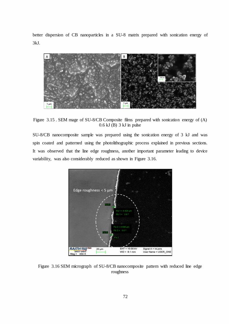
72
better dispersion of CB nanoparticles in a SU-8 matrix prepared with sonication energy of
3kJ.
Figure 3.15 . SEM mage of SU-8/CB Composite films prepared with sonication energy of (A) 0.6 kJ (B) 3 kJ in pulse
SU-8/CB nanocomposite sample was prepared using the sonication energy of 3 kJ and was
spin coated and patterned using the photolithographic process explained in previous sections.
It was observed that the line edge roughness, another important parameter leading to device
variability, was also considerably reduced as shown in Figure 3.16.
Figure 3.16 SEM micrograph of SU-8/CB nanocomposite pattern with reduced line edge roughness
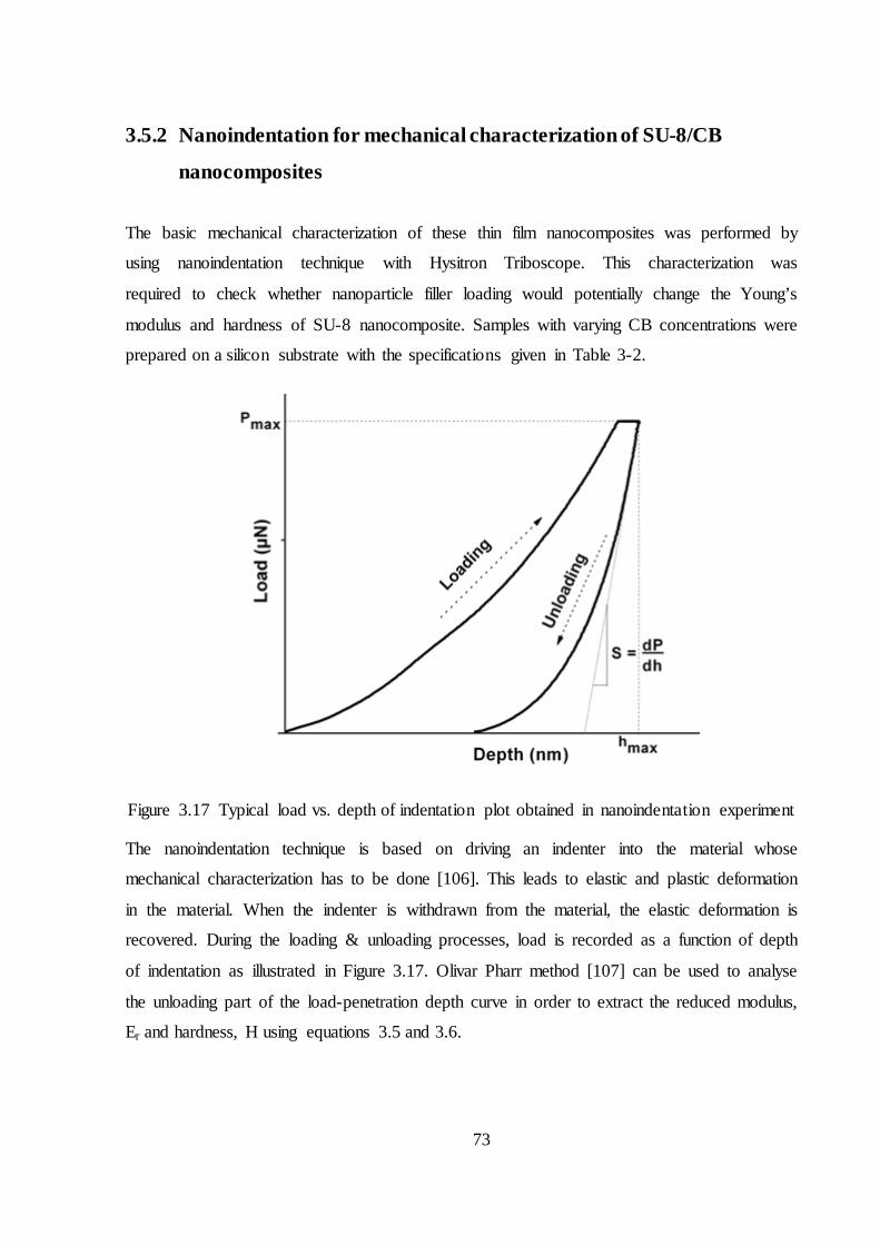
73
3.5.2 Nanoindentation for mechanical characterization of SU-8/CB
nanocomposites
The basic mechanical characterization of these thin film nanocomposites was performed by
using nanoindentation technique with Hysitron Triboscope. This characterization was
required to check whether nanoparticle filler loading would potentially change the Young’s
modulus and hardness of SU-8 nanocomposite. Samples with varying CB concentrations were
prepared on a silicon substrate with the specifications given in Table 3-2.
Figure 3.17 Typical load vs. depth of indentation plot obtained in nanoindentation experiment
The nanoindentation technique is based on driving an indenter into the material whose
mechanical characterization has to be done [106]. This leads to elastic and plastic deformation
in the material. When the indenter is withdrawn from the material, the elastic deformation is
recovered. During the loading & unloading processes, load is recorded as a function of depth
of indentation as illustrated in Figure 3.17. Olivar Pharr method [107] can be used to analyse
the unloading part of the load-penetration depth curve in order to extract the reduced modulus,
Er and hardness, H using equations 3.5 and 3.6.
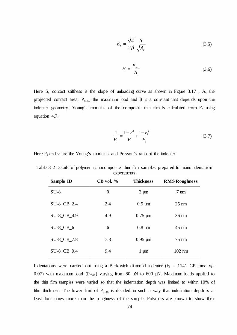
74
2rc
SEA
(3.5)
max
c
PHA
(3.6)
Here S, contact stiffness is the slope of unloading curve as shown in Figure 3.17 , Ac the
projected contact area, Pmax the maximum load and β is a constant that depends upon the
indenter geometry. Young’s modulus of the composite thin film is calculated from Er using
equation 4.7.
22 11 1 i
r iE E E
(3.7)
Here Ei and νi are the Young’s modulus and Poisson’s ratio of the indenter.
Table 3-2 Details of polymer nanocomposite thin film samples prepared for nanoindentation experiments
Sample ID CB vol. % Thickness RMS Roughness
SU-8 0 2 µm 7 nm
SU-8_CB_2.4 2.4 0.5 µm 25 nm
SU-8_CB_4.9 4.9 0.75 µm 36 nm
SU-8_CB_6 6 0.8 µm 45 nm
SU-8_CB_7.8 7.8 0.95 µm 75 nm
SU-8_CB_9.4 9.4 1 µm 102 nm
Indentations were carried out using a Berkovich diamond indenter (Ei = 1141 GPa and νi=
0.07) with maximum load (Pmax) varying from 80 µN to 600 µN. Maximum loads applied to
the thin film samples were varied so that the indentation depth was limited to within 10% of
film thickness. The lower limit of Pmax is decided in such a way that indentation depth is at
least four times more than the roughness of the sample. Polymers are known to show their

75
peculiar viscoelastic behavior while indenting and in order to minimize the effect of
viscoelasticity high loading and unloading rates were used [108]. The viscoelastic behaviour
if present would be indicated with the presence of a “nose” in the force curve due to the
increase in penetration depth even during the unloading portion of the load curve.
Figure 3.18 Load versus indentation depth for different loads. Inset: Scanned image of a set of
indents in SU-8
Load-indentation depth curves for different Pmax values are shown in Figure 3.18 along with
an array of Berkovich indents on the SU-8 surface. It can be noticed that viscoelastic
behaviour is not seen in these load curves.
Young’s moduli and hardness values for different load-depth curves were extracted using the
method explained above and are shown as a function of maximum indentation depth in Figure
3.19. Young’s modulus tends to increase for higher depth of indentation, whereas hardness
does not show a significant variation with indentation depths. It is widely accepted that for
depths of indentation greater than 10% of film thickness, substrate interaction effects are
observed. This can be clearly seen in Figure 3.19, where the dotted line indicates 10% of film
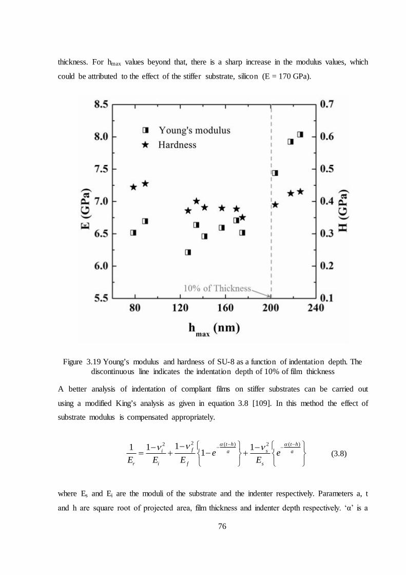
76
thickness. For hmax values beyond that, there is a sharp increase in the modulus values, which
could be attributed to the effect of the stiffer substrate, silicon (E = 170 GPa).
Figure 3.19 Young’s modulus and hardness of SU-8 as a function of indentation depth. The discontinuous line indicates the indentation depth of 10% of film thickness
A better analysis of indentation of compliant films on stiffer substrates can be carried out
using a modified King’s analysis as given in equation 3.8 [109]. In this method the effect of
substrate modulus is compensated appropriately.
2 ( ) ( )2 211 11 1t h t h
fi sa a
r i f s
e eE E E E
(3.8)
where Es and Ei are the moduli of the substrate and the indenter respectively. Parameters a, t
and h are square root of projected area, film thickness and indenter depth respectively. ‘α’ is a
77
fitting parameter which is obtained from King’s plot [109] based on the value of normalized
punch size, a / (t-h). The calculated modulus as a function of indentation depth based on the
modified King’s analysis is given in Figure 3.20 (A).
Figure 3.20 (A) Young’s modulus of SU-8 as a function of indentation depth after modified King’s analysis. (B)Young’s Modulus of SU-8/CB composite as a function of CB Vol %.
Here all the samples were indented with Pmax = 450 N
Similarly Young’s moduli and hardness for other samples with different CB concentrations
were also calculated. Here the data shown is for indentations carried out for an array of
indents carried out at a Pmax of 450 N. Modulus values were found to increase with
increasing CB filler loading (Figure 3.20 (B)). This agrees reasonably well with two existing
theories for particulate filled polymer nanocomposites with spherical fillers, namely parallel
mixing model (ref. equation 3.9) and the modified Guth’s model (ref. equation
3.10)[110,111].
m m f fE V E V E (3.9)
21 2.5 14.1m f fE E V V
(3.10)
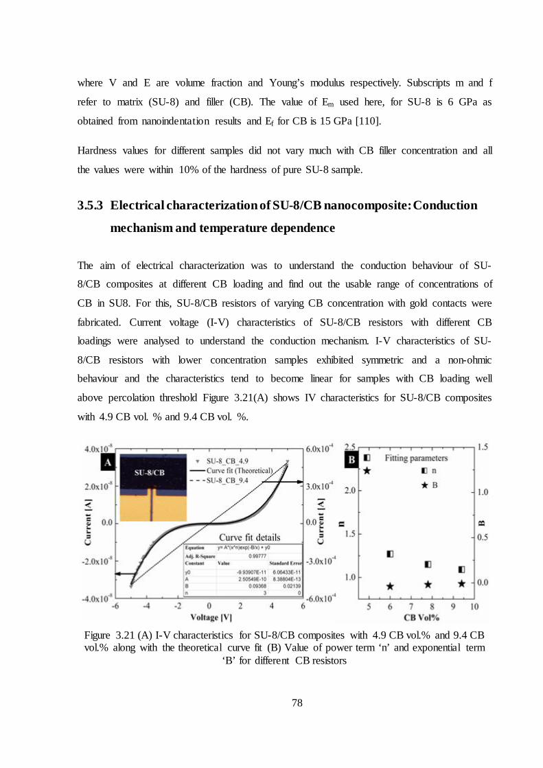
78
where V and E are volume fraction and Young’s modulus respectively. Subscripts m and f
refer to matrix (SU-8) and filler (CB). The value of Em used here, for SU-8 is 6 GPa as
obtained from nanoindentation results and Ef for CB is 15 GPa [110].
Hardness values for different samples did not vary much with CB filler concentration and all
the values were within 10% of the hardness of pure SU-8 sample.
3.5.3 Electrical characterization of SU-8/CB nanocomposite: Conduction
mechanism and temperature dependence
The aim of electrical characterization was to understand the conduction behaviour of SU-
8/CB composites at different CB loading and find out the usable range of concentrations of
CB in SU8. For this, SU-8/CB resistors of varying CB concentration with gold contacts were
fabricated. Current voltage (I-V) characteristics of SU-8/CB resistors with different CB
loadings were analysed to understand the conduction mechanism. I-V characteristics of SU-
8/CB resistors with lower concentration samples exhibited symmetric and a non-ohmic
behaviour and the characteristics tend to become linear for samples with CB loading well
above percolation threshold Figure 3.21(A) shows IV characteristics for SU-8/CB composites
with 4.9 CB vol. % and 9.4 CB vol. %.
Figure 3.21 (A) I-V characteristics for SU-8/CB composites with 4.9 CB vol.% and 9.4 CB vol.% along with the theoretical curve fit (B) Value of power term ‘n’ and exponential term
‘B’ for different CB resistors
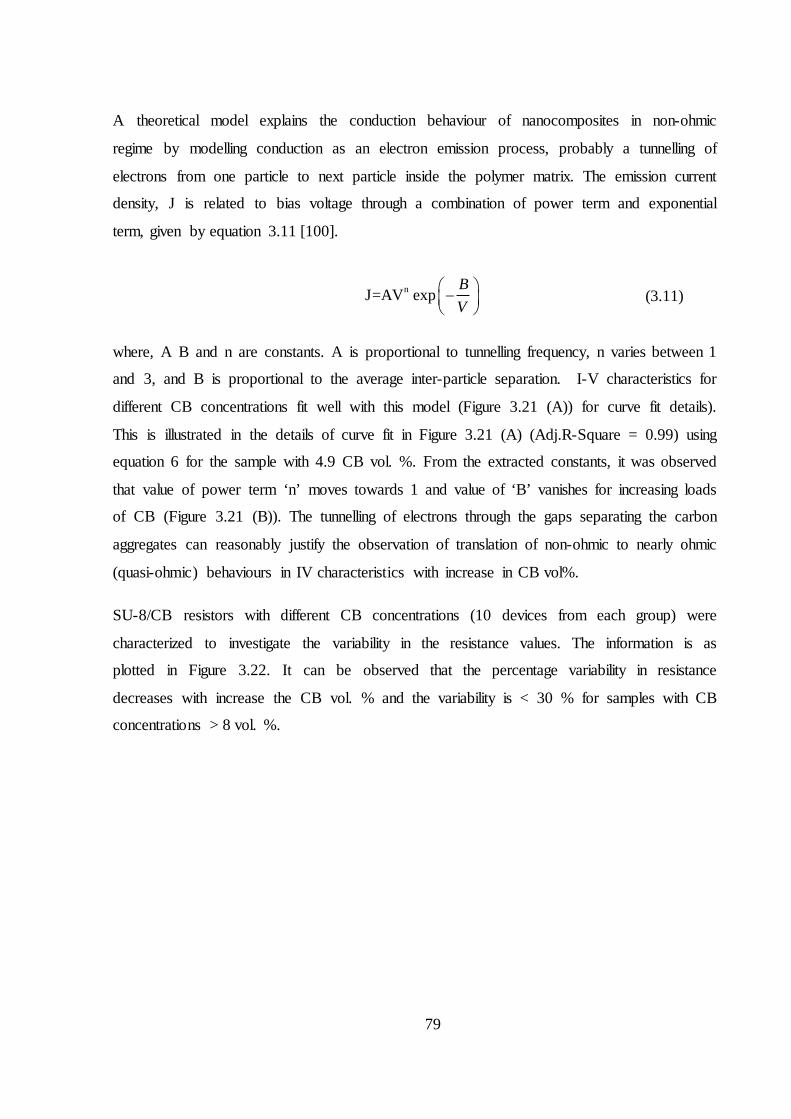
79
A theoretical model explains the conduction behaviour of nanocomposites in non-ohmic
regime by modelling conduction as an electron emission process, probably a tunnelling of
electrons from one particle to next particle inside the polymer matrix. The emission current
density, J is related to bias voltage through a combination of power term and exponential
term, given by equation 3.11 [100].
nJ=AV expBV
(3.11)
where, A B and n are constants. A is proportional to tunnelling frequency, n varies between 1
and 3, and B is proportional to the average inter-particle separation. I-V characteristics for
different CB concentrations fit well with this model (Figure 3.21 (A)) for curve fit details).
This is illustrated in the details of curve fit in Figure 3.21 (A) (Adj.R-Square = 0.99) using
equation 6 for the sample with 4.9 CB vol. %. From the extracted constants, it was observed
that value of power term ‘n’ moves towards 1 and value of ‘B’ vanishes for increasing loads
of CB (Figure 3.21 (B)). The tunnelling of electrons through the gaps separating the carbon
aggregates can reasonably justify the observation of translation of non-ohmic to nearly ohmic
(quasi-ohmic) behaviours in IV characteristics with increase in CB vol%.
SU-8/CB resistors with different CB concentrations (10 devices from each group) were
characterized to investigate the variability in the resistance values. The information is as
plotted in Figure 3.22. It can be observed that the percentage variability in resistance
decreases with increase the CB vol. % and the variability is < 30 % for samples with CB
concentrations > 8 vol. %.
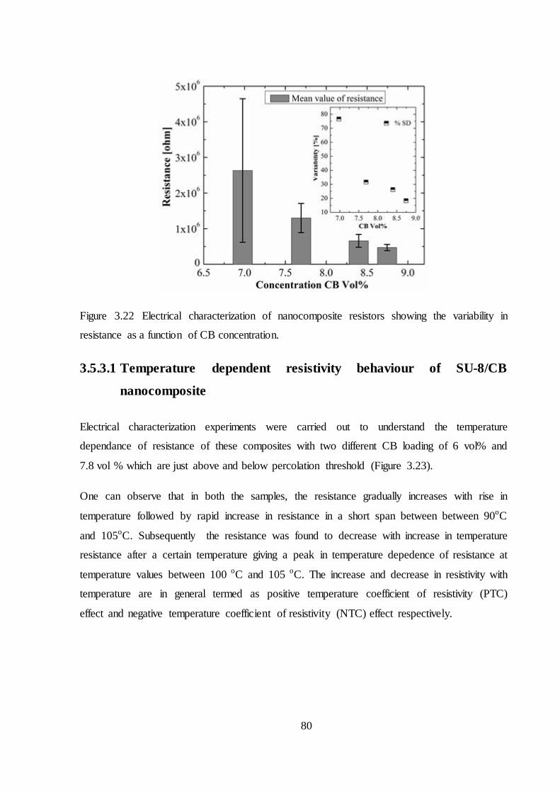
80
Figure 3.22 Electrical characterization of nanocomposite resistors showing the variability in
resistance as a function of CB concentration.
3.5.3.1 Temperature dependent resistivity behaviour of SU-8/CB
nanocomposite
Electrical characterization experiments were carried out to understand the temperature
dependance of resistance of these composites with two different CB loading of 6 vol% and
7.8 vol % which are just above and below percolation threshold (Figure 3.23).
One can observe that in both the samples, the resistance gradually increases with rise in
temperature followed by rapid increase in resistance in a short span between between 90oC
and 105oC. Subsequently the resistance was found to decrease with increase in temperature
resistance after a certain temperature giving a peak in temperature depedence of resistance at
temperature values between 100 oC and 105 oC. The increase and decrease in resistivity with
temperature are in general termed as positive temperature coefficient of resistivity (PTC)
effect and negative temperature coefficient of resistivity (NTC) effect respectively.
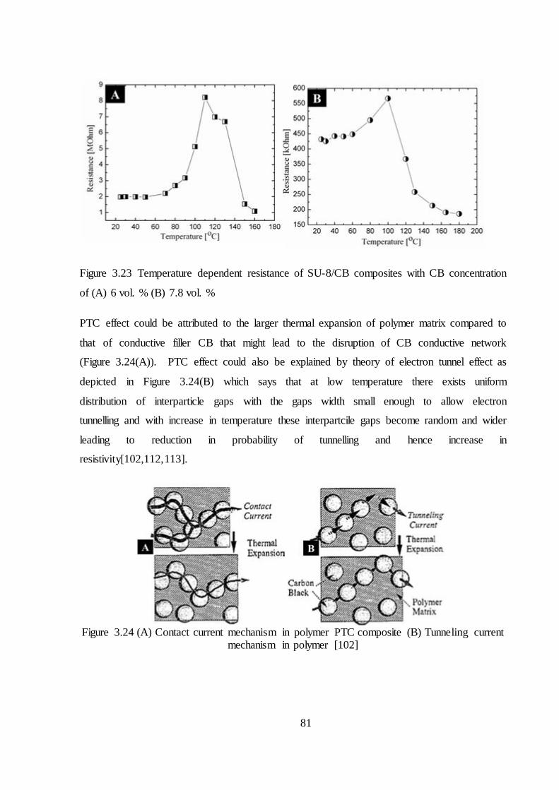
81
Figure 3.23 Temperature dependent resistance of SU-8/CB composites with CB concentration
of (A) 6 vol. % (B) 7.8 vol. %
PTC effect could be attributed to the larger thermal expansion of polymer matrix compared to
that of conductive filler CB that might lead to the disruption of CB conductive network
(Figure 3.24(A)). PTC effect could also be explained by theory of electron tunnel effect as
depicted in Figure 3.24(B) which says that at low temperature there exists uniform
distribution of interparticle gaps with the gaps width small enough to allow electron
tunnelling and with increase in temperature these interpartcile gaps become random and wider
leading to reduction in probability of tunnelling and hence increase in
resistivity[102,112,113].
Figure 3.24 (A) Contact current mechanism in polymer PTC composite (B) Tunneling current
mechanism in polymer [102] A
82
The NTC effect might be due to densification of SU-8 polymer with progressive crosslinking
above the highest temperature of the latest bake cycle during the processing (~95oC). This
densification leads to decrease in distance between the conductive CB particles and hence
decrease in resistivity of the SU-8/CB nanocomposite. It was also observed that samples with
lower filler, CB loadings, exhibited strong temperature dependent resistivity behaviour.
3.5.4 Design and fabrication of SU-8/CB nanocomposite microcantilevers
with improved sensor performance
Second generation SU-8 nanocomposite microcantilevers were designed with new parameters
and were fabricated based on the knowhow obtained from the systematic characterization
experiments detailed in the previous sections. The design for polymer nanocomposite
microcantilever is chosen in order to improve the surface stress sensitivity, common mode
rejection, mechanical stability and packaging compatibility of the sensor. Dimensions of
microcantilevers are decided based on stiffness and resonance frequency of microcantilever
which are the two important mechanical properties of beams for mechanical sensitivity and
stability under external vibrations. The resonance frequency should be greater than 5 kHz so
that mechanical noise would not excite the microcantilever. The thicknesses of individual SU-
8 layers were chosen in order to keep the piezoresistive SU-8 nanocomposite layer away from
neutral axis to improve the piezoresistive sensitivity, while considering the microfabrication
constraints for SU-8. SU-8 cantilever die contains two sets of measurement and reference
cantilevers as depicted in the planar and cross sectional schematic of the polymer device die
(Figure 3.25).

83
Figure 3.25 Device design schematic. (A) Planar schematic (B).Cross sectional schematic of SU-8 cantilever with embedded SU-8/CB composite.
Other than the “U” shaped cantilevers, “V” shaped cantilevers were also designed as part of
the same mask. Mechanical stability of “V” shaped cantilevers was known to better compared
to that of simple rectangular cantilevers and it has got inherent advantage of reducing the
lateral torsion.
For the SU-8/CB nanocomposite piezoresistor, optimum carbon black filler loading in the
range of 8 – 9 vol. % was chosen based on the following requirements and the justification
provided in the previous section based on the material characterization data. (i) Low Young’s
modulus: for this, the CB concentration is kept as low as possible. (ii) UV patternability of the
SU-8/CB nanocomposite with minimum possible edge roughness: the quality of patterns
worsens for SU-8/CB samples for CB filler loadings > 9 vol.%. (iii) Good strain sensitivity:
SU-8/CB composites with CB concentrations just above the percolation threshold are
expected to give the maximum strain sensitivity. (iv) Ohmic conduction behaviour and
minimum variability in conduction: the variability in SU-8/CB resistance values decreases
with increase in CB concentration.
The fabrication of this device structure involves the defining of individual layers on a dummy
substrate, silicon and release of the whole polymer structure from the silicon substrate.
The detailed process sequence with individual layer patterns is illustrated in Figure 3.26.
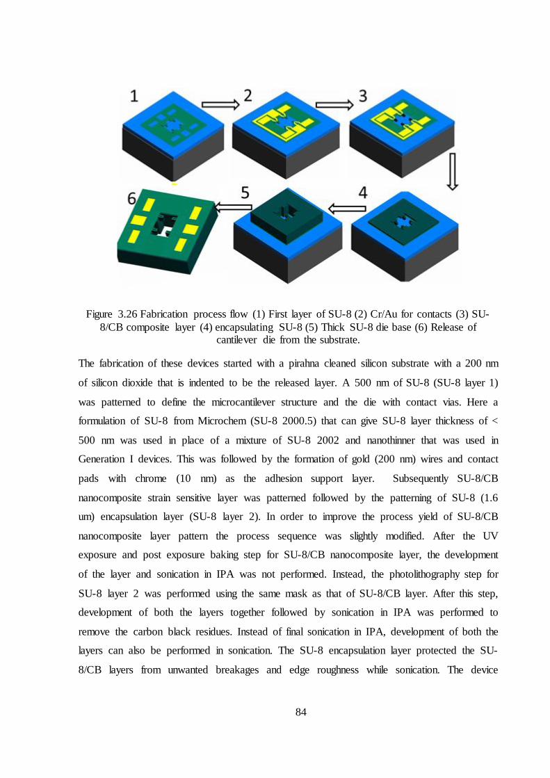
84
Figure 3.26 Fabrication process flow (1) First layer of SU-8 (2) Cr/Au for contacts (3) SU-8/CB composite layer (4) encapsulating SU-8 (5) Thick SU-8 die base (6) Release of
cantilever die from the substrate.
The fabrication of these devices started with a pirahna cleaned silicon substrate with a 200 nm
of silicon dioxide that is indented to be the released layer. A 500 nm of SU-8 (SU-8 layer 1)
was patterned to define the microcantilever structure and the die with contact vias. Here a
formulation of SU-8 from Microchem (SU-8 2000.5) that can give SU-8 layer thickness of <
500 nm was used in place of a mixture of SU-8 2002 and nanothinner that was used in
Generation I devices. This was followed by the formation of gold (200 nm) wires and contact
pads with chrome (10 nm) as the adhesion support layer. Subsequently SU-8/CB
nanocomposite strain sensitive layer was patterned followed by the patterning of SU-8 (1.6
um) encapsulation layer (SU-8 layer 2). In order to improve the process yield of SU-8/CB
nanocomposite layer pattern the process sequence was slightly modified. After the UV
exposure and post exposure baking step for SU-8/CB nanocomposite layer, the development
of the layer and sonication in IPA was not performed. Instead, the photolithography step for
SU-8 layer 2 was performed using the same mask as that of SU-8/CB layer. After this step,
development of both the layers together followed by sonication in IPA was performed to
remove the carbon black residues. Instead of final sonication in IPA, development of both the
layers can also be performed in sonication. The SU-8 encapsulation layer protected the SU-
8/CB layers from unwanted breakages and edge roughness while sonication. The device
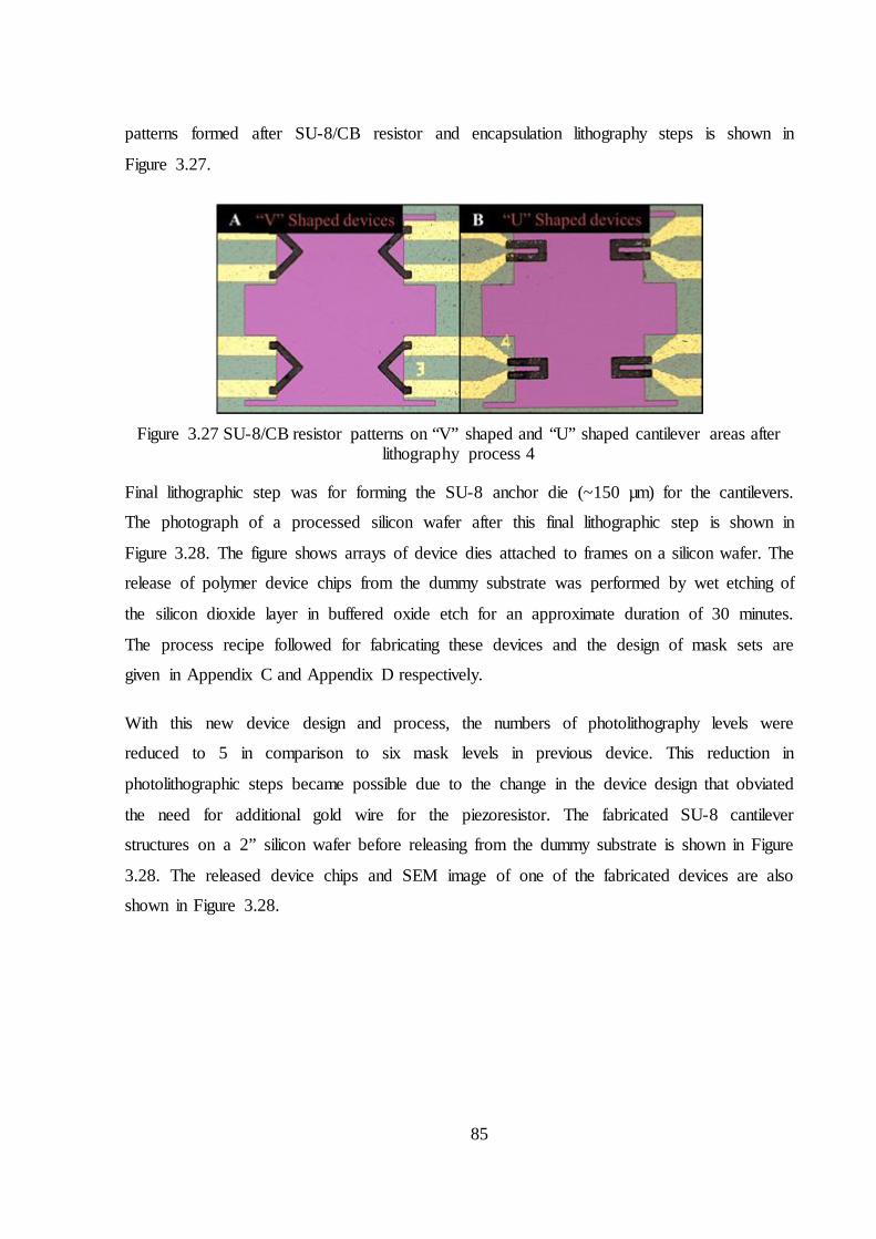
85
patterns formed after SU-8/CB resistor and encapsulation lithography steps is shown in
Figure 3.27.
Figure 3.27 SU-8/CB resistor patterns on “V” shaped and “U” shaped cantilever areas after
lithography process 4
Final lithographic step was for forming the SU-8 anchor die (~150 µm) for the cantilevers.
The photograph of a processed silicon wafer after this final lithographic step is shown in
Figure 3.28. The figure shows arrays of device dies attached to frames on a silicon wafer. The
release of polymer device chips from the dummy substrate was performed by wet etching of
the silicon dioxide layer in buffered oxide etch for an approximate duration of 30 minutes.
The process recipe followed for fabricating these devices and the design of mask sets are
given in Appendix C and Appendix D respectively.
With this new device design and process, the numbers of photolithography levels were
reduced to 5 in comparison to six mask levels in previous device. This reduction in
photolithographic steps became possible due to the change in the device design that obviated
the need for additional gold wire for the piezoresistor. The fabricated SU-8 cantilever
structures on a 2” silicon wafer before releasing from the dummy substrate is shown in Figure
3.28. The released device chips and SEM image of one of the fabricated devices are also
shown in Figure 3.28.
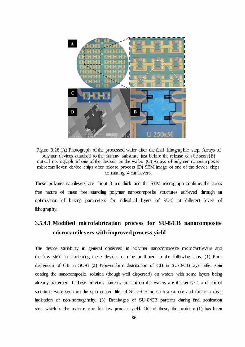
86
Figure 3.28 (A) Photograph of the processed wafer after the final lithographic step. Arrays of polymer devices attached to the dummy substrate just before the release can be seen (B)
optical micrograph of one of the devices on the wafer. (C) Arrays of polymer nanocomposite microcantilever device chips after release process (D) SEM image of one of the device chips
containing 4 cantilevers.
These polymer cantilevers are about 3 µm thick and the SEM micrograph confirms the stress
free nature of these free standing polymer nanocomposite structures achieved through an
optimization of baking parameters for individual layers of SU-8 at different levels of
lithography.
3.5.4.1 Modified microfabrication process for SU-8/CB nanocomposite microcantilevers with improved process yield
The device variability in general observed in polymer nanocomposite microcantilevers and
the low yield in fabricating these devices can be attributed to the following facts. (1) Poor
dispersion of CB in SU-8 (2) Non-uniform distribution of CB in SU-8/CB layer after spin
coating the nanocomposite solution (though well dispersed) on wafers with some layers being
already patterned. If these previous patterns present on the wafers are thicker (> 1 m), lot of
striations were seen on the spin coated film of SU-8/CB on such a sample and this is a clear
indication of non-homogeneity. (3) Breakages of SU-8/CB patterns during final sonication
step which is the main reason for low process yield. Out of these, the problem (1) has been
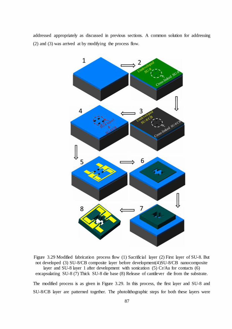
87
addressed appropriately as discussed in previous sections. A common solution for addressing
(2) and (3) was arrived at by modifying the process flow.
Figure 3.29 Modified fabrication process flow (1) Sacrificial layer (2) First layer of SU-8. But not developed (3) SU-8/CB composite layer before development(4)SU-8/CB nanocomposite
layer and SU-8 layer 1 after development with sonication (5) Cr/Au for contacts (6) encapsulating SU-8 (7) Thick SU-8 die base (8) Release of cantilever die from the substrate.
The modified process is as given in Figure 3.29. In this process, the first layer and SU-8 and
SU-8/CB layer are patterned together. The photolithographic steps for both these layers were
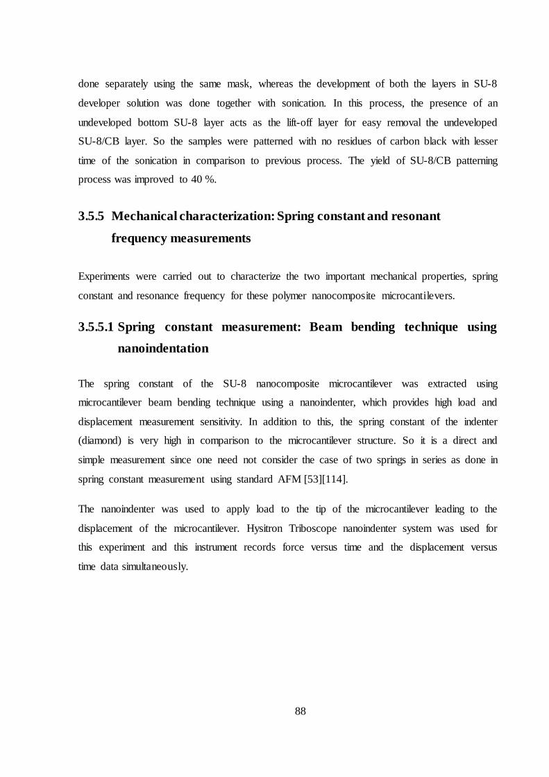
88
done separately using the same mask, whereas the development of both the layers in SU-8
developer solution was done together with sonication. In this process, the presence of an
undeveloped bottom SU-8 layer acts as the lift-off layer for easy removal the undeveloped
SU-8/CB layer. So the samples were patterned with no residues of carbon black with lesser
time of the sonication in comparison to previous process. The yield of SU-8/CB patterning
process was improved to 40 %.
3.5.5 Mechanical characterization: Spring constant and resonant
frequency measurements
Experiments were carried out to characterize the two important mechanical properties, spring
constant and resonance frequency for these polymer nanocomposite microcantilevers.
3.5.5.1 Spring constant measurement: Beam bending technique using nanoindentation
The spring constant of the SU-8 nanocomposite microcantilever was extracted using
microcantilever beam bending technique using a nanoindenter, which provides high load and
displacement measurement sensitivity. In addition to this, the spring constant of the indenter
(diamond) is very high in comparison to the microcantilever structure. So it is a direct and
simple measurement since one need not consider the case of two springs in series as done in
spring constant measurement using standard AFM [53][114].
The nanoindenter was used to apply load to the tip of the microcantilever leading to the
displacement of the microcantilever. Hysitron Triboscope nanoindenter system was used for
this experiment and this instrument records force versus time and the displacement versus
time data simultaneously.
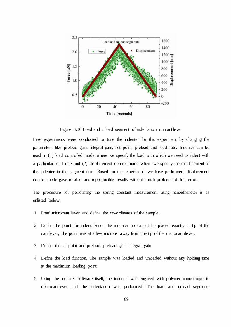
89
Figure 3.30 Load and unload segment of indentation on cantilever
Few experiments were conducted to tune the indenter for this experiment by changing the
parameters like preload gain, integral gain, set point, preload and load rate. Indenter can be
used in (1) load controlled mode where we specify the load with which we need to indent with
a particular load rate and (2) displacement control mode where we specify the displacement of
the indenter in the segment time. Based on the experiments we have performed, displacement
control mode gave reliable and reproducible results without much problem of drift error.
The procedure for performing the spring constant measurement using nanoidneneter is as
enlisted below.
1. Load microcantilever and define the co-ordinates of the sample.
2. Define the point for indent. Since the indenter tip cannot be placed exactly at tip of the
cantilever, the point was at a few microns away from the tip of the microcantilever.
3. Define the set point and preload, preload gain, integral gain.
4. Define the load function. The sample was loaded and unloaded without any holding time
at the maximum loading point.
5. Using the indenter software itself, the indenter was engaged with polymer nanocomposite
microcantilever and the indentation was performed. The load and unload segments
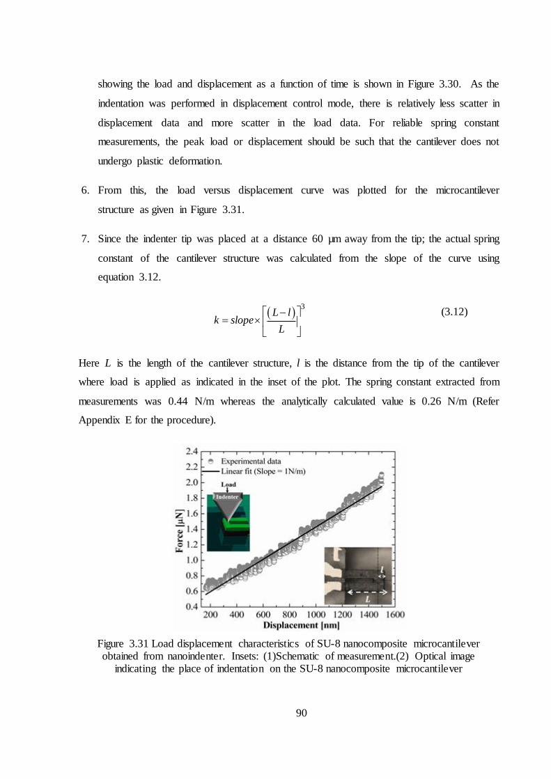
90
showing the load and displacement as a function of time is shown in Figure 3.30. As the
indentation was performed in displacement control mode, there is relatively less scatter in
displacement data and more scatter in the load data. For reliable spring constant
measurements, the peak load or displacement should be such that the cantilever does not
undergo plastic deformation.
6. From this, the load versus displacement curve was plotted for the microcantilever
structure as given in Figure 3.31.
7. Since the indenter tip was placed at a distance 60 µm away from the tip; the actual spring
constant of the cantilever structure was calculated from the slope of the curve using
equation 3.12.
3L lk slope
L
(3.12)
Here L is the length of the cantilever structure, l is the distance from the tip of the cantilever
where load is applied as indicated in the inset of the plot. The spring constant extracted from
measurements was 0.44 N/m whereas the analytically calculated value is 0.26 N/m (Refer
Appendix E for the procedure).
Figure 3.31 Load displacement characteristics of SU-8 nanocomposite microcantilever obtained from nanoindenter. Insets: (1)Schematic of measurement.(2) Optical image
indicating the place of indentation on the SU-8 nanocomposite microcantilever
91
3.5.5.2 Resonance Frequency using LDV
For resonance frequency measurements, the experimentation was performed with Polytec
Laser Doppler Vibrometer1(LDV). Microcantilever die was attached to a piezo buzzzer which
provided the actuation. The laser beam from the LDV was directed to the cantilever surface.
The vibration amplitude and frequency were extracted from the doppler shift of the laser
beam frequency due to the motion of the cantilever. The output of an LDV is a continuous
analog voltage that is proportional to the target velocity component along the direction of the
laser beam. When the structure is excited at its natural frequencies, the structure will start to
show its mode shapes. Hence from the frequency response obtained from LDV, the resonant
frequency of the structure can be obtained. The resonant frequency plot obtained from the
LDV for SU-8 nanocomposite microcantilevers (CB concentration of 8.4 vol. %) is given in
Figure 3.32. These microcantilevers were coated with 30 nm of Au.
Figure 3.32 Frequency plot from Laser Doppler Vibrometer (A) “U” shaped cantilever(B)
“V” shaped cantilever
Measured resonant frequency for “U shaped and “V” shaped microcantilevers were 22.6 kHz
and 38.8 kHz respectively. This is closer to the analytically calculated value (~ 20 kHz for
“U” shaped microcantilever) obtained by following the case of multilayer composite
cantilever beam given in Appendix E. Since the resonance frequency of the device is higher
than 5 kHz, it would not be affected by external mechanical vibrations.
1 The LDV measurements performed at IISC Bangalore.
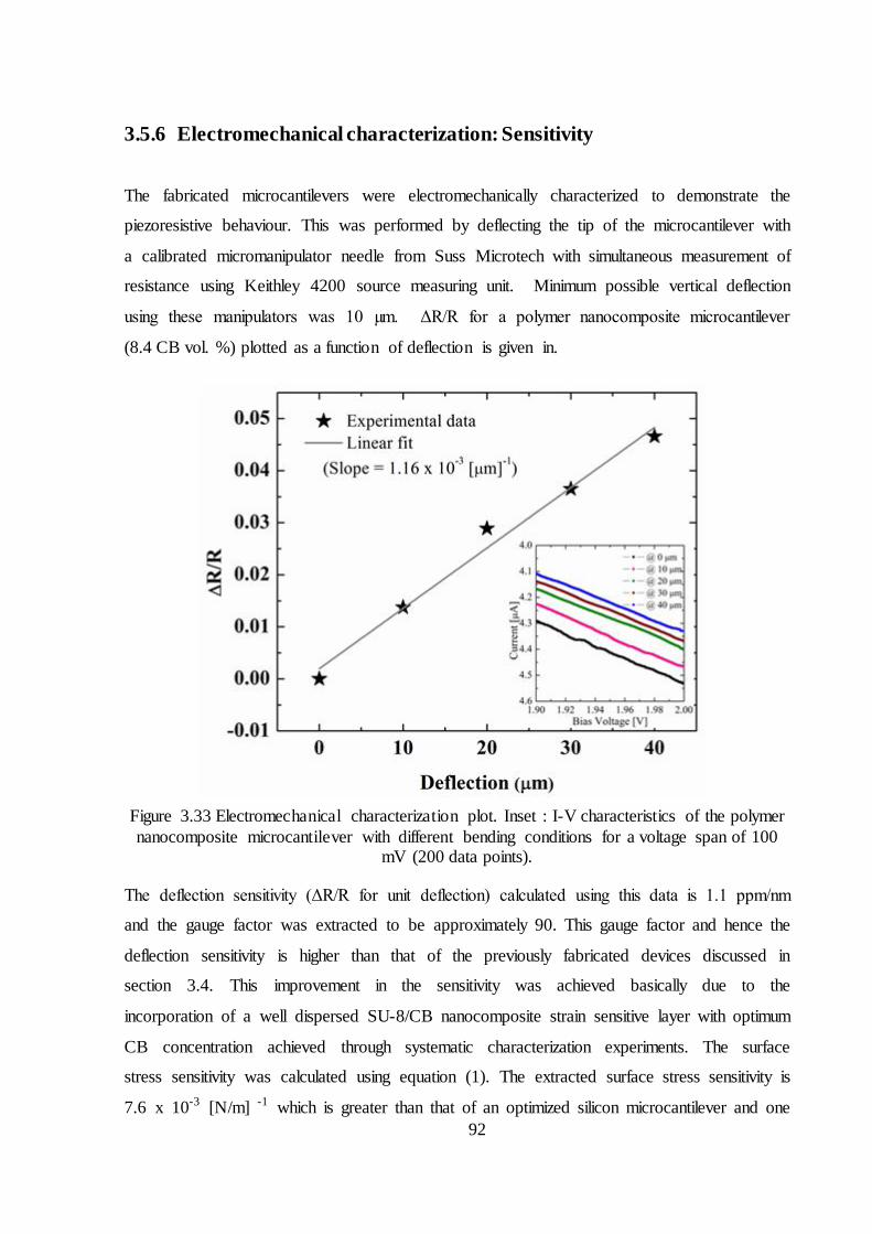
92
3.5.6 Electromechanical characterization: Sensitivity
The fabricated microcantilevers were electromechanically characterized to demonstrate the
piezoresistive behaviour. This was performed by deflecting the tip of the microcantilever with
a calibrated micromanipulator needle from Suss Microtech with simultaneous measurement of
resistance using Keithley 4200 source measuring unit. Minimum possible vertical deflection
using these manipulators was 10 µm. ΔR/R for a polymer nanocomposite microcantilever
(8.4 CB vol. %) plotted as a function of deflection is given in.
Figure 3.33 Electromechanical characterization plot. Inset : I-V characteristics of the polymer nanocomposite microcantilever with different bending conditions for a voltage span of 100
mV (200 data points).
The deflection sensitivity (ΔR/R for unit deflection) calculated using this data is 1.1 ppm/nm
and the gauge factor was extracted to be approximately 90. This gauge factor and hence the
deflection sensitivity is higher than that of the previously fabricated devices discussed in
section 3.4. This improvement in the sensitivity was achieved basically due to the
incorporation of a well dispersed SU-8/CB nanocomposite strain sensitive layer with optimum
CB concentration achieved through systematic characterization experiments. The surface
stress sensitivity was calculated using equation (1). The extracted surface stress sensitivity is
7.6 x 10⁻³ [N/m] -1 which is greater than that of an optimized silicon microcantilever and one
93
order of magnitude higher than that of polymer microcantilevers with Au as the strain gauge
[115] reported in literature. Further improvement can be achieved by tuning the thickness and
shape of the polymer microcantilever structure.
Polymer nanocomposite microcantilevers with lower concentration were also
electromechanically characterized. It was observed that for devices with 7 vol.% CB, the
deflection sensitivity was found to be around 20 ppm /nm and this increased sensitivity is
attributed to the CB concentration nearing percolation threshold. But because of the same
reason, the variability of these low CB concentration devices is also higher (Figure 3.22). So
until the availability of ‘device variability aware design’ for the interface electronics, these
lower concentration devices might not be considered for bio/chemical sensing applications.
3.5.7 Noise characterization
The performance evaluation of a piezoresistive microcantilever sensor is not complete just by
estimating their sensitivity. The resolution of the measurement signal decides the minimum
detectable surface stress or minimum detectable deflection using these polymer
nanomechanical microcantilever sensors. The measurement signal resolution is limited by the
noise originating from the piezoresistor. The two major and important sources of noise in
piezoresistors are (1) Johnson Noise and (2) Hooge noise which is also known as 1/f noise
[42]. Thermal fluctuations of charge carriers cause the Johnson noise and this noise is
frequency independent. The Hooge noise or 1/f noise is an electrical noise that dominates at
smaller frequencies and falls off at high frequencies. According to Hooge’s model [116], the
power spectral density of this noise is inversely proportional to the number of carriers in the
resistor and it increases with increase in bias voltage of the resistor. The total noise power
spectral density can be obtained by adding the all the noise components. The noise level is
obtained by integrating the noise power spectral density over the measurement bandwidth.
The noise spectrum of SU-8/CB nanocomposite microcantilevers with different CB
concentrations were recorded using a noise measurement set up with the schematic shown in
Figure 3.34 .
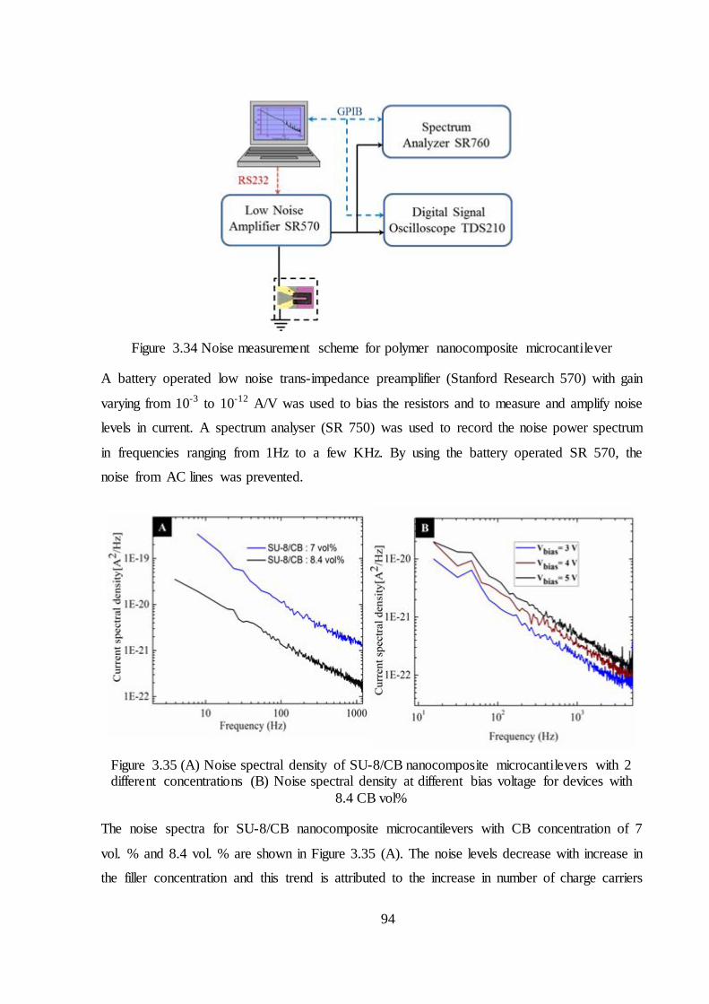
94
Figure 3.34 Noise measurement scheme for polymer nanocomposite microcantilever
A battery operated low noise trans-impedance preamplifier (Stanford Research 570) with gain
varying from 10-3 to 10-12 A/V was used to bias the resistors and to measure and amplify noise
levels in current. A spectrum analyser (SR 750) was used to record the noise power spectrum
in frequencies ranging from 1Hz to a few KHz. By using the battery operated SR 570, the
noise from AC lines was prevented.
Figure 3.35 (A) Noise spectral density of SU-8/CB nanocomposite microcantilevers with 2 different concentrations (B) Noise spectral density at different bias voltage for devices with
8.4 CB vol%
The noise spectra for SU-8/CB nanocomposite microcantilevers with CB concentration of 7
vol. % and 8.4 vol. % are shown in Figure 3.35 (A). The noise levels decrease with increase in
the filler concentration and this trend is attributed to the increase in number of charge carriers
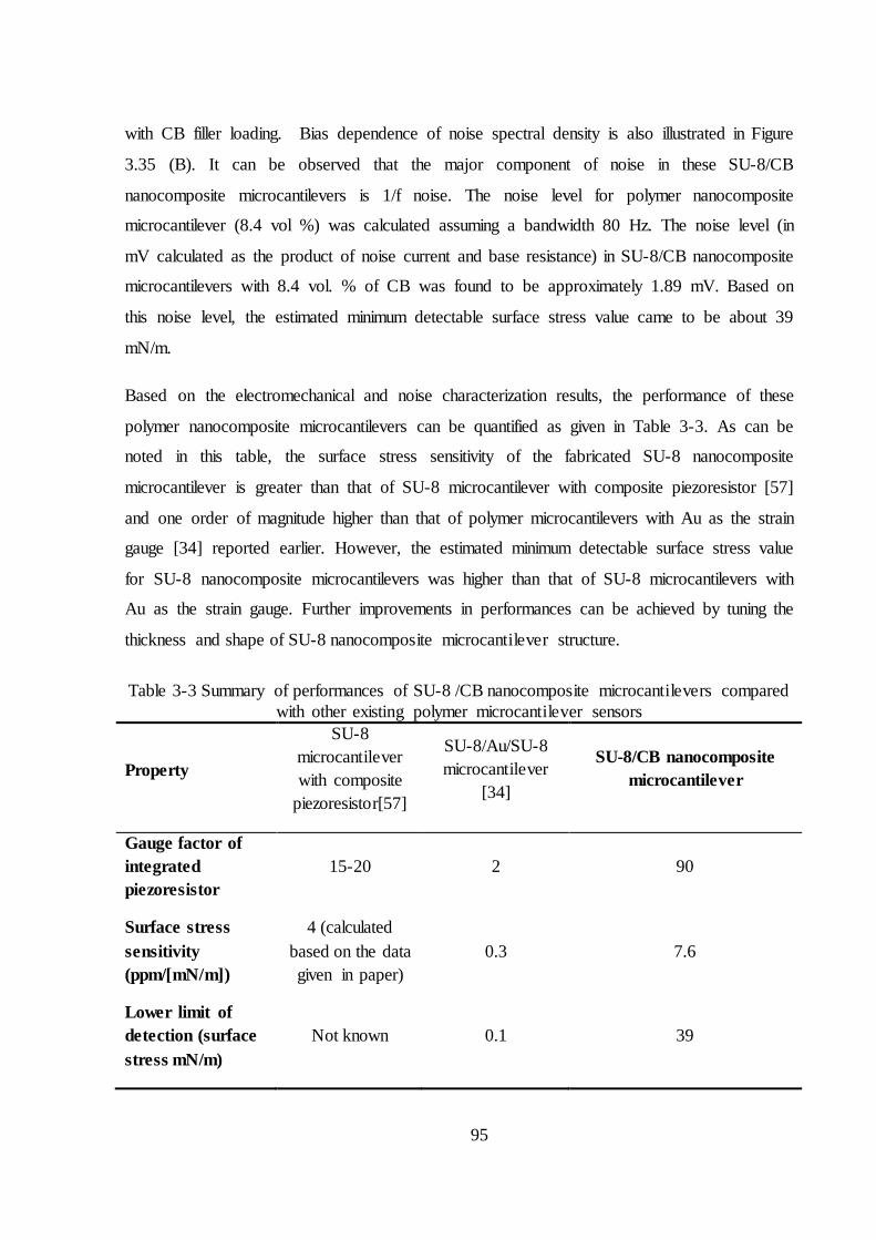
95
with CB filler loading. Bias dependence of noise spectral density is also illustrated in Figure
3.35 (B). It can be observed that the major component of noise in these SU-8/CB
nanocomposite microcantilevers is 1/f noise. The noise level for polymer nanocomposite
microcantilever (8.4 vol %) was calculated assuming a bandwidth 80 Hz. The noise level (in
mV calculated as the product of noise current and base resistance) in SU-8/CB nanocomposite
microcantilevers with 8.4 vol. % of CB was found to be approximately 1.89 mV. Based on
this noise level, the estimated minimum detectable surface stress value came to be about 39
mN/m.
Based on the electromechanical and noise characterization results, the performance of these
polymer nanocomposite microcantilevers can be quantified as given in Table 3-3. As can be
noted in this table, the surface stress sensitivity of the fabricated SU-8 nanocomposite
microcantilever is greater than that of SU-8 microcantilever with composite piezoresistor [57]
and one order of magnitude higher than that of polymer microcantilevers with Au as the strain
gauge [34] reported earlier. However, the estimated minimum detectable surface stress value
for SU-8 nanocomposite microcantilevers was higher than that of SU-8 microcantilevers with
Au as the strain gauge. Further improvements in performances can be achieved by tuning the
thickness and shape of SU-8 nanocomposite microcantilever structure.
Table 3-3 Summary of performances of SU-8 /CB nanocomposite microcantilevers compared with other existing polymer microcantilever sensors
Property
SU-8 microcantilever with composite
piezoresistor[57]
SU-8/Au/SU-8 microcantilever
[34]
SU-8/CB nanocomposite microcantilever
Gauge factor of integrated piezoresistor
15-20 2 90
Surface stress sensitivity (ppm/[mN/m])
4 (calculated based on the data given in paper)
0.3 7.6
Lower limit of detection (surface stress mN/m)
Not known 0.1 39

96
The SU-8 nanocomposite devices exhibited high noise levels which lead to lower resolution
in sensing as compared that of silicon based piezoresistive microcantilevers. However, they
possess higher sensitivity and the polymer nanocomposite microcantilever fabrication process
tends to be simple and cost effective compared to that of silicon based microcantilevers and
this makes them suitable for a variety of low cost bio/chemical sensing applications which
could make this technology extremely attractive.
3.6 Summary
In summary, the development of a polymer nanomechanical cantilever bio/chemical sensors
with embedded polymer nanocomposite as the piezoresistive layer has been presented. The
summary of the key aspects covered in this chapter are enlisted below.
[1] SU-8/CB composites were prepared by ultrasonic mixing of SU-8 2002, Nanothinner and
Carbon Black, Conductex 7067 Ultra. Experimental results on photolithographic
patterning and basic conductivity studies the composite with different CB filler
concentrations were presented. The percolation threshold achieved with the process was
6.5 wt.% which is less than that reported for similar composite in [57].
[2] Design and fabrication of SU-8 microcantilevers with embedded polymer nanocomposite
(SU-8/CB) piezoresistor was presented. The microcantilevers had an overall stack
thickness of just 3 µm compared to 7 µm in [57].
[3] Characterization of these devices was performed to measure the deflection and surface
stress sensitivity. The deflection sensitivity of these cantilevers was found to be 0.55
ppm/nm. The surface stress sensitivity for these devices is 4.1x10⁻³ [N/m]-1 which is
more than 10 times the sensitivity of the SU-8 cantilever with Au and at least a factor of
two higher compared to the reported result on SU-8/CB cantilevers.
[4] Systematic and more detailed material characterizations were performed for improving
the device performance and efficiency of fabrication process. Improvement in dispersion
characteristics of SU-8/CB composites was achieved with characterization study
conducted with dynamic light scattering technique. SU-8/CB composites with different
CB concentrations were prepared with improved CB dispersion in order to find out the
effect of varying CB filler concentration on the mechanical and electrical characteristics
97
of the polymer nanocomposite. This has been done for identifying the optimal range of
CB concentrations for improved device performance. Using nanoindentation experiments
for SU-8/CB composite, effect of CB filler loading on the mechanical properties of the
composites were studied. Young’s modulus was observed to increase with CB loading
and the values for 8 vol% samples were about 30-40% higher compared to a pure SU-8
sample. Electrical conduction behaviour and the device to device resistance variability of
SU-8/CB nanocomposite with different CB loading were analysed. Device variability was
observed to be decreasing with increasing concentrations of CB and the variability was <
30 % for samples with CB concentrations > 8 vol. %. Based on these characterization
results, the preferable range of concentration of CB in SU-8 turned out to be 8 – 9 vol. %
.
[5] SU-8 microcantilevers with embedded SU-8/CB nanocomposite piezoresistor having
optimum carbon black filler loading in the range of 8 – 9 vol. % were designed and
fabricated. The design for polymer nanocomposite microcantilever was chosen in order to
improve the surface stress sensitivity, common mode rejection, mechanical stability and
packaging compatibility of the sensor with an additional benefit of reduction in process
complexity.
[6] The experimentally determined resonance frequency and spring constant for the
fabricated polymer nanocomposite cantilever of thickness 3 µm were 22.6 kHz and
0.44N/m respectively. These devices exhibited surface stress sensitivity of 7.6 x 10⁻³
[N/m]-1 which is greater than that of an optimized silicon microcantilever and one order
of magnitude higher than that of polymer microcantilevers with Au as the strain gauge.
The noise spectrum of polymer nanocomposite microcantilevers indicated that the major
component of noise in these devices was 1/f noise. Though the polymer nanocomposite
devices showed higher noise levels compared to that of silicon based piezoresistive
microcantilevers, their higher sensitivity supports their suitability for low cost
bio/chemical sensing applications.
[7] A novel polymer MEMS accelerometer with SU-8/Carbon black as a piezoresistor was
also designed and fabricated. This was the first time demonstration of a piezoresistive
polymer accelerometer. The device design, fabrication and characterization of the device
is presented in Appendix 2.
98
Chapter 4
Detection of Explosive Vapours using Polymer
Nanocomposite Microcantilevers
4.1 Introduction
Receptor based detection of explosive vapours using microcantilevers works on the principle
of translation of target molecule-receptor binding into nanomechanical motion of the
microcantilever. As per the current literature available, microcantilever that have been used
for these applications are mostly silicon or derived materials such as silicon dioxide and
silicon nitride. The major challenge in explosive vapour detection is that sensor should be able
to detect the explosive molecules in very low concentrations. So there is always a need for
more sensitive microcantilever sensing platforms. So polymer nanocomposite microcantilever
with their very good surface stress sensitivity might be a good candidate for these
applications. Also developing an application using these polymer nanocomposite
microcantilevers would help in understanding the real time challenges using these
microcantilevers as a platform technology for different sensing applications.
99
In order to use polymer nanocomposite microcantilevers for explosive detection, the
cantilever surface needs to be coated or functionalized with a receptor ie., a chemically
selective layer for the target molecule. As mentioned in Chapter 2, 4-MBA (4-
Mercaptobenzoic acid, also known as thiosalicylic acid) is chosen as the receptor layer as the
most popular explosives such as TNT, RDX and PETN are known to bind with 4-MBA
[117,118]. 4-MBA forms stable self-assembled monolayers (SAM) on Au. 4-MBA is acidic in
nature due to the presence of –COOH group that can dissociate into a –COO- charged group.
The SAM provides well oriented –COOH groups for efficient binding of vapour phase bases
like explosives.
Polymer nanocomposite microcantilevers (CB concentrations of 8.4 vol. %) were
functionalized using 4-MBA by following the functionalization procedure detailed in Chapter
2 for single layer SU-8 microcantilevers.
4.2 Explosive Vapour Experiments
Functionalized microcantilevers had to be attached to a custom designed PCB for further
characterization. Wire-bonding technique was tried out for making connections between
device contact pads and PCB contacts. But the device contact pads were getting damaged
during wire bonding. This is basically because of the thin contact pads of 180 nm of PVD
deposited gold on SU-8. Electroplated Au contact pads could have been a viable option to
solve this issue. However the process and masks had to be adapted in order to accommodate
the gold electroplating step. So in place of wire-bonding, a low temperature curable 2-part
epoxy, Epotek H20E (Epoxy Technologies) was used to make the contact lines from device to
PCB. The curing was performed in an oven at 80oC for 3 hours.
The functionalized microcantilever along with non-functionalized microcantilever as
reference microcantilever were attached to a PCB using insulating epoxy (EPO-TEK H70E)
with contacts made using conducting silver epoxy (EPO-TEK H20E)). The microcantilevers
were kept inside a PTFE gas flow cell (25 mm diameter) with a proper ‘O’ ring seal. The PCB
was partially placed inside the flow cell, so that the microcantilevers are inside the flow cell
and the PCB contacts were available outside the flow cell for making connections to the
circuit. The microcantilever PCB and the arrangement of PTFE gas flow cell and the circuit
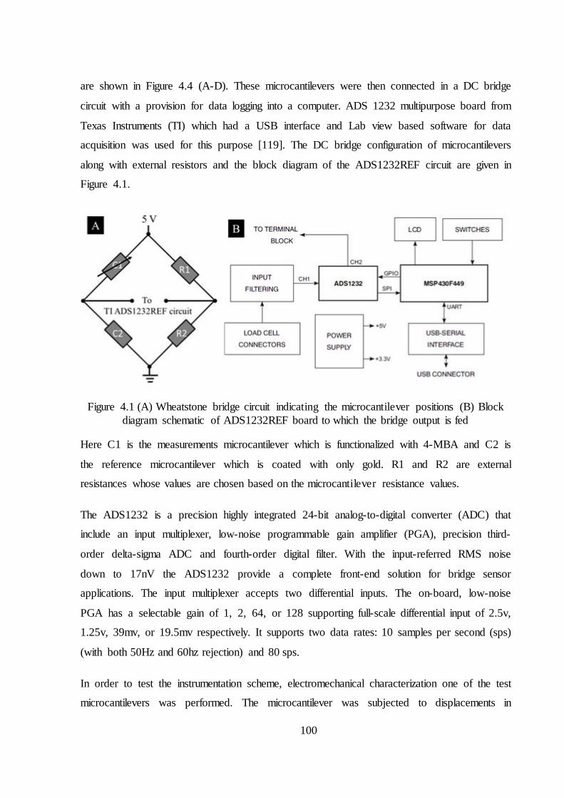
100
are shown in Figure 4.4 (A-D). These microcantilevers were then connected in a DC bridge
circuit with a provision for data logging into a computer. ADS 1232 multipurpose board from
Texas Instruments (TI) which had a USB interface and Lab view based software for data
acquisition was used for this purpose [119]. The DC bridge configuration of microcantilevers
along with external resistors and the block diagram of the ADS1232REF circuit are given in
Figure 4.1.
Figure 4.1 (A) Wheatstone bridge circuit indicating the microcantilever positions (B) Block diagram schematic of ADS1232REF board to which the bridge output is fed
Here C1 is the measurements microcantilever which is functionalized with 4-MBA and C2 is
the reference microcantilever which is coated with only gold. R1 and R2 are external
resistances whose values are chosen based on the microcantilever resistance values.
The ADS1232 is a precision highly integrated 24-bit analog-to-digital converter (ADC) that
include an input multiplexer, low-noise programmable gain amplifier (PGA), precision third-
order delta-sigma ADC and fourth-order digital filter. With the input-referred RMS noise
down to 17nV the ADS1232 provide a complete front-end solution for bridge sensor
applications. The input multiplexer accepts two differential inputs. The on-board, low-noise
PGA has a selectable gain of 1, 2, 64, or 128 supporting full-scale differential input of 2.5v,
1.25v, 39mv, or 19.5mv respectively. It supports two data rates: 10 samples per second (sps)
(with both 50Hz and 60hz rejection) and 80 sps.
In order to test the instrumentation scheme, electromechanical characterization one of the test
microcantilevers was performed. The microcantilever was subjected to displacements in
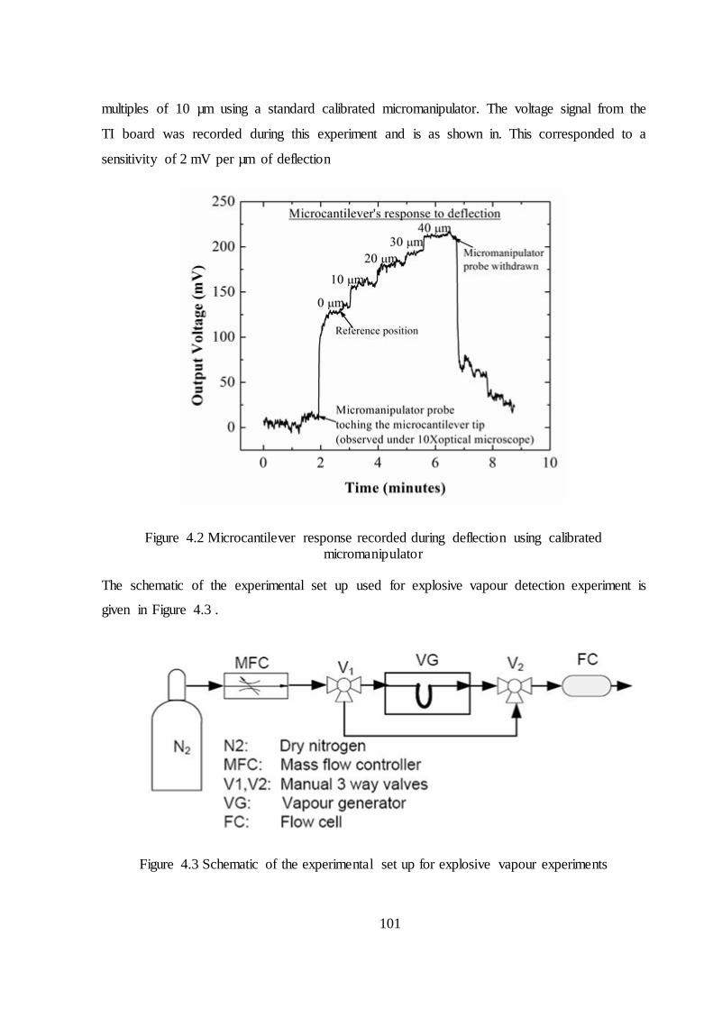
101
multiples of 10 µm using a standard calibrated micromanipulator. The voltage signal from the
TI board was recorded during this experiment and is as shown in. This corresponded to a
sensitivity of 2 mV per µm of deflection
Figure 4.2 Microcantilever response recorded during deflection using calibrated micromanipulator
The schematic of the experimental set up used for explosive vapour detection experiment is
given in Figure 4.3 .
Figure 4.3 Schematic of the experimental set up for explosive vapour experiments
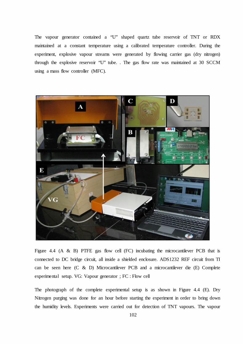
102
The vapour generator contained a “U” shaped quartz tube reservoir of TNT or RDX
maintained at a constant temperature using a calibrated temperature controller. During the
experiment, explosive vapour streams were generated by flowing carrier gas (dry nitrogen)
through the explosive reservoir “U” tube. . The gas flow rate was maintained at 30 SCCM
using a mass flow controller (MFC).
Figure 4.4 (A & B) PTFE gas flow cell (FC) incubating the microcantilever PCB that is
connected to DC bridge circuit, all inside a shielded enclosure. ADS1232 REF circuit from TI
can be seen here (C & D) Microcantilever PCB and a microcantilever die (E) Complete
experimental setup. VG: Vapour generator ; FC : Flow cell
The photograph of the complete experimental setup is as shown in Figure 4.4 (E). Dry
Nitrogen purging was done for an hour before starting the experiment in order to bring down
the humidity levels. Experiments were carried out for detection of TNT vapours. The vapour

103
generator had been calibrated for TNT concentrations at different temperatures using Gas
chromatography/Mass spectroscopy (GC/MS) and the calibration data is as given in Figure
4.5.
Figure 4.5 Calibration of TNT vapour generator at different temperature2
For TNT vapour exposure experiment, TNT “U” tube reservoir was maintained at 65oC.
During the experiment, TNT vapour streams were generated by flowing dry nitrogen through
the TNT reservoir. In order to switch from TNT vapour, the same nitrogen gas flow was
maintained through the microcantilever gas flow cell by redirecting the nitrogen flow stream
through a bypass line. This switching between TNT vapour stream and dry nitrogen stream
was performed using 3-way valves V1 and V2 indicated in the schematic (Figure 4.3).
Extrapolating the calibration curve (Figure 4.5) for 65oC, TNT vapour concentration was
approximately 30 ppb. Microcantilever response for alternating cycles of TNT (~30 ppb) and
2 TNT concentrations were calculated from the TNT vapour generator calibration data obtained from Dr. Pramod Soni, TBRL.
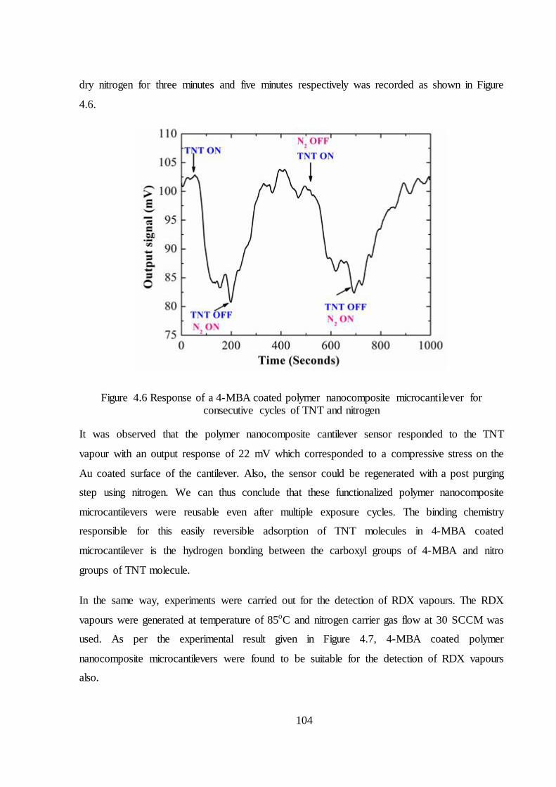
104
dry nitrogen for three minutes and five minutes respectively was recorded as shown in Figure
4.6.
Figure 4.6 Response of a 4-MBA coated polymer nanocomposite microcantilever for consecutive cycles of TNT and nitrogen
It was observed that the polymer nanocomposite cantilever sensor responded to the TNT
vapour with an output response of 22 mV which corresponded to a compressive stress on the
Au coated surface of the cantilever. Also, the sensor could be regenerated with a post purging
step using nitrogen. We can thus conclude that these functionalized polymer nanocomposite
microcantilevers were reusable even after multiple exposure cycles. The binding chemistry
responsible for this easily reversible adsorption of TNT molecules in 4-MBA coated
microcantilever is the hydrogen bonding between the carboxyl groups of 4-MBA and nitro
groups of TNT molecule.
In the same way, experiments were carried out for the detection of RDX vapours. The RDX
vapours were generated at temperature of 85oC and nitrogen carrier gas flow at 30 SCCM was
used. As per the experimental result given in Figure 4.7, 4-MBA coated polymer
nanocomposite microcantilevers were found to be suitable for the detection of RDX vapours
also.
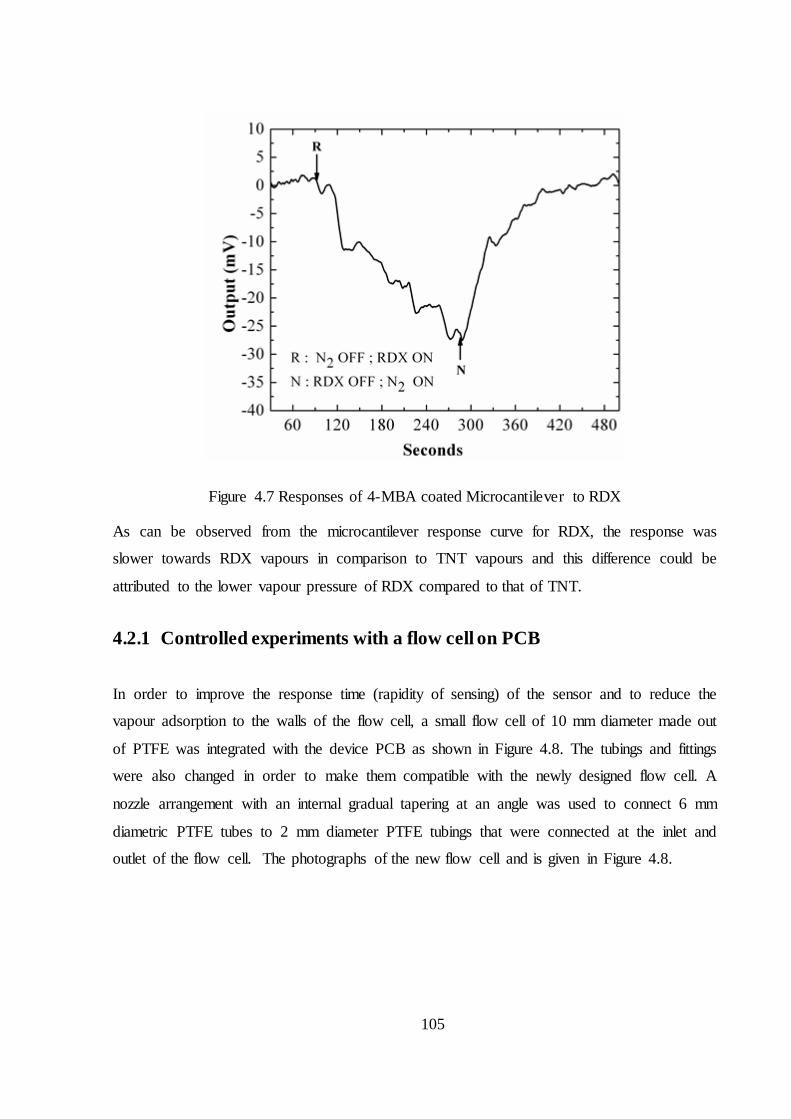
105
Figure 4.7 Responses of 4-MBA coated Microcantilever to RDX
As can be observed from the microcantilever response curve for RDX, the response was
slower towards RDX vapours in comparison to TNT vapours and this difference could be
attributed to the lower vapour pressure of RDX compared to that of TNT.
4.2.1 Controlled experiments with a flow cell on PCB
In order to improve the response time (rapidity of sensing) of the sensor and to reduce the
vapour adsorption to the walls of the flow cell, a small flow cell of 10 mm diameter made out
of PTFE was integrated with the device PCB as shown in Figure 4.8. The tubings and fittings
were also changed in order to make them compatible with the newly designed flow cell. A
nozzle arrangement with an internal gradual tapering at an angle was used to connect 6 mm
diametric PTFE tubes to 2 mm diameter PTFE tubings that were connected at the inlet and
outlet of the flow cell. The photographs of the new flow cell and is given in Figure 4.8.
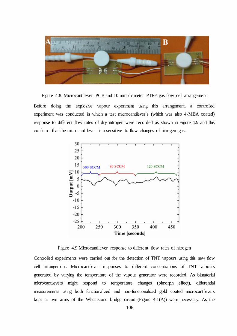
106
Figure 4.8. Microcantilever PCB and 10 mm diameter PTFE gas flow cell arrangement
Before doing the explosive vapour experiment using this arrangement, a controlled
experiment was conducted in which a test microcantilever’s (which was also 4-MBA coated)
response to different flow rates of dry nitrogen were recorded as shown in Figure 4.9 and this
confirms that the microcantilever is insensitive to flow changes of nitrogen gas.
Figure 4.9 Microcantilever response to different flow rates of nitrogen
Controlled experiments were carried out for the detection of TNT vapours using this new flow
cell arrangement. Microcantilever responses to different concentrations of TNT vapours
generated by varying the temperature of the vapour generator were recorded. As bimaterial
microcantilevers might respond to temperature changes (bimorph effect), differential
measurements using both functionalized and non-functionalized gold coated microcantilevers
kept at two arms of the Wheatstone bridge circuit (Figure 4.1(A)) were necessary. As the
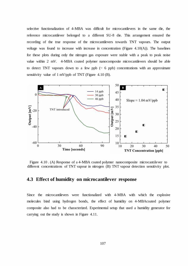
107
selective functionalization of 4-MBA was difficult for microcantilevers in the same die, the
reference microcantilever belonged to a different SU-8 die. This arrangement ensured the
recording of the true response of the microcantilevers towards TNT vapours. The output
voltage was found to increase with increase in concentration (Figure 4.10(A)). The baselines
for these plots during only the nitrogen gas exposure were stable with a peak to peak noise
value within 2 mV. 4-MBA coated polymer nanocomposite microcantilevers should be able
to detect TNT vapours down to a few ppb (~ 6 ppb) concentrations with an approximate
sensitivity value of 1 mV/ppb of TNT (Figure 4.10 (B).
Figure 4.10 . (A) Response of a 4-MBA coated polymer nanocomposite microcantilever to different concentrations of TNT vapour in nitrogen (B) TNT vapour detection sensitivity plot.
4.3 Effect of humidity on microcantilever response
Since the microcantilevers were functionalized with 4-MBA with which the explosive
molecules bind using hydrogen bonds, the effect of humidity on 4-MBAcoated polymer
composite also had to be characterized. Experimental setup that used a humidity generator for
carrying out the study is shown in Figure 4.11.
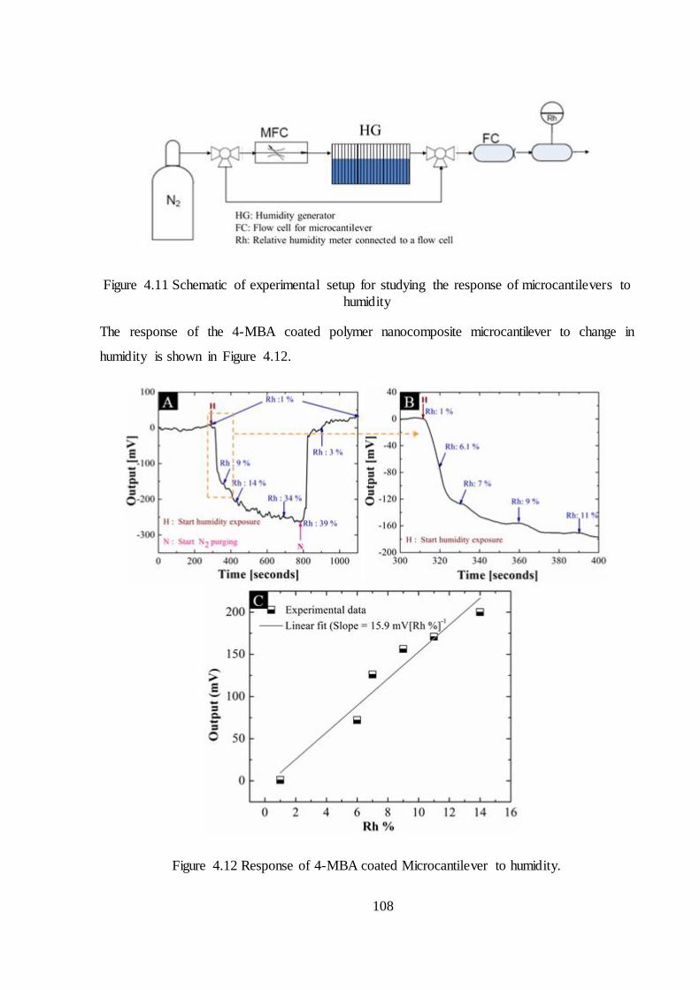
108
Figure 4.11 Schematic of experimental setup for studying the response of microcantilevers to humidity
The response of the 4-MBA coated polymer nanocomposite microcantilever to change in
humidity is shown in Figure 4.12.
Figure 4.12 Response of 4-MBA coated Microcantilever to humidity.
109
The microcantilever output signal was found to be increasing with increase in humidity levels
and the signal went back to near the original value as humidity levels were decreased with dry
nitrogen stream. It was observed that there was a change in voltage of 200 mV for a relative
humidity change of 13 % (Figure 4.12). Water is a polar solvent and so it forms hydrogen
bonds with other polar molecules and with itself. In the case of exposure of a 4-MBA coated
microcantilever, water molecules form hydrogen bonds with –COOH group of 4-MBA which
causes a surface stress change on the microcantilever. As the water molecule can form
hydrogen bonds with itself, this adsorption induced surface stress increases with increase in
humidity levels.
From this study on response of 4-MBA coated polymer nanocomposite microcantilevers
towards variation in humidity levels, one can realize that selectivity could be a major concern
in detecting explosive vapour molecules using microcantilevers functionalized with molecules
such as 4-MBA with which unwanted molecules such as water molecules that adsorb easily
by formation of hydrogen bond. However this selectivity problem related to humidity has
been partially addressed for these 4-MBA functionalized microcantilevers. For this,
experiments were conducted to study the response of the microcantilever to trace TNT in
normal ambient in place of controlled experiments using vapour generator and dry nitrogen
source arrangement. Microcantilevers were placed in the flow cell in the same way as
explained in controlled explosive vapour experiments. A DC pump [1.4 litre/min] was
incorporated at the outlet of cantilever flow cell in order to sample the air with forced
circulation. This was used in place of MFC. Microcantilever response was recorded while
sampling the ambient air using the pump and this was continued for stabilizing the signal
(Figure 4.13). TNT trace sample was brought near the inlet of the flow cell and the sensor
responded indicating the presence of TNT. As per the literature available, the approximate
TNT concentration in air can be 4 ppb at room temperature [120]. During this part of the
cycle the pump takes in the TNT along with the ambient air. When the TNT source was taken
away (by closing the vial containing TNT), the sensor signal went back to the original level
(Figure 4.13). The pump was on throughout the experiment. The ambient air took the role of
purging the adsorbed TNT on 4-MBA and bringing the sensor back to the status where only
ambient air was present which might be at a specific level of humidity. Another cycle of
experiment was carried out with exposure to trace RDX source as depicted in Figure 4.13. As
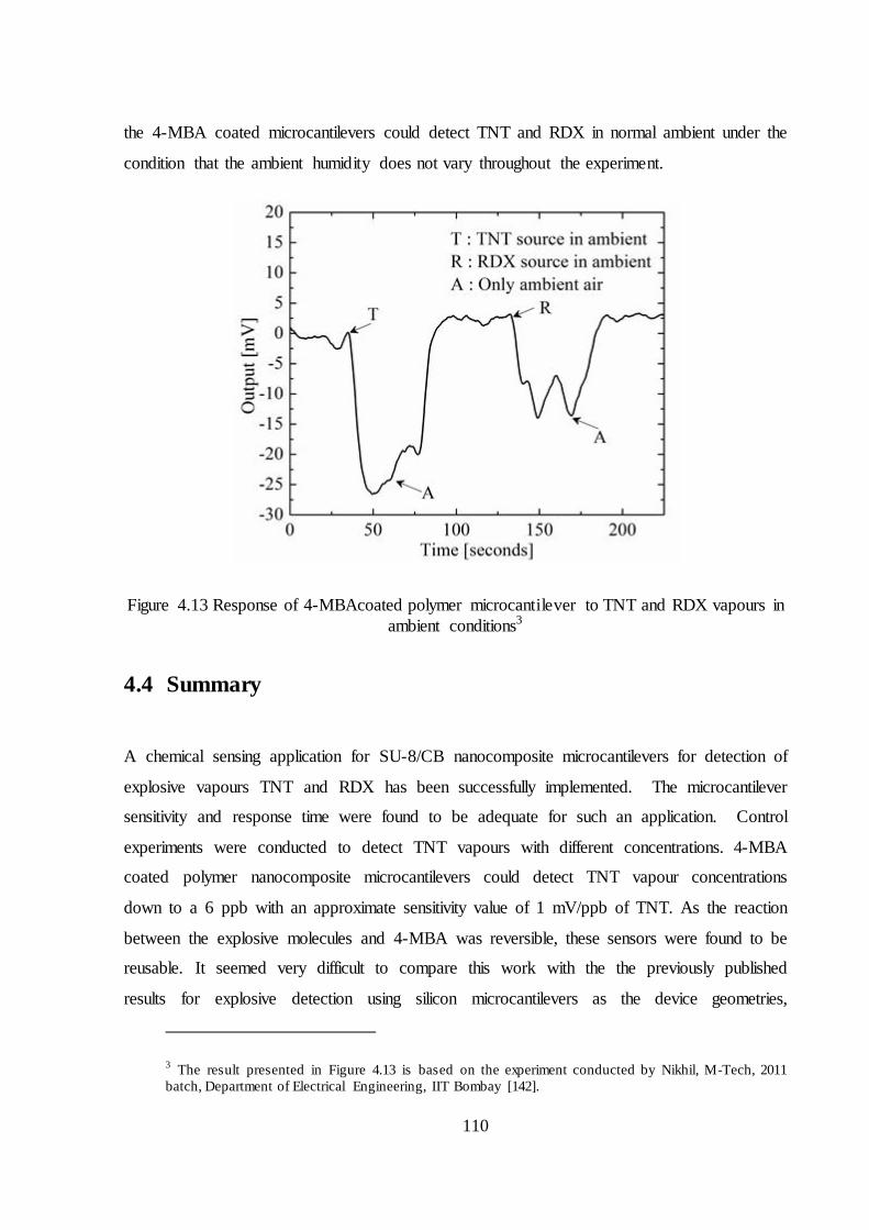
110
the 4-MBA coated microcantilevers could detect TNT and RDX in normal ambient under the
condition that the ambient humidity does not vary throughout the experiment.
Figure 4.13 Response of 4-MBAcoated polymer microcantilever to TNT and RDX vapours in ambient conditions3
4.4 Summary
A chemical sensing application for SU-8/CB nanocomposite microcantilevers for detection of
explosive vapours TNT and RDX has been successfully implemented. The microcantilever
sensitivity and response time were found to be adequate for such an application. Control
experiments were conducted to detect TNT vapours with different concentrations. 4-MBA
coated polymer nanocomposite microcantilevers could detect TNT vapour concentrations
down to a 6 ppb with an approximate sensitivity value of 1 mV/ppb of TNT. As the reaction
between the explosive molecules and 4-MBA was reversible, these sensors were found to be
reusable. It seemed very difficult to compare this work with the the previously published
results for explosive detection using silicon microcantilevers as the device geometries,
3 The result presented in Figure 4.13 is based on the experiment conducted by Nikhil, M-Tech, 2011 batch, Department of Electrical Engineering, IIT Bombay [142].
111
functionalization materials and methods and the electronic instrumentation schemes and
systems were different. However the main focus of this thesis was to optimize the material
and the fabrication aspects for the polymer nanocomposite cantilever platform in order to
improve their surface stress sensitivity so as to demonstrate their potential for bio/chemical
sensing applications. With the help of this part of the work, the potential of this cost effective
and ultra-sensitive polymer nanocomposite microcantilever sensing platform for a typical, yet
challenging chemical sensing application was demonstrated.
For a sensor, selectivity is as important as sensitivity. Explosive vapour exposure experiments
presented in this Chapter were conducted by isolating secondary effects such as ambient
humidity changes. However, a set of dedicated experiments were conducted in order to the
test the effect of ambient humidity. The results obtained based on the experiments conducted
to test the effect of humidity changes on 4-MBA coated SU-8 nanocomposite
microcantilevers were alarming as the sensor was responding to humidity changes with a
better sensitivity compared to that of explosive vapours. The hydrogen bond between 4-MBA
and water molecules was responsible for this. However, the experiments conducted using
microcantilevers functionalized with 4-MBA for detection of TNT and RDX in ambient
conditions could support their candidature for detection of explosive vapours in ambient
where the humidity levels do not vary within a measurement cycle. In addition, such
secondary effects can be solved either by using microcantilever array approach with separate
coatings that support different types of interactions with the analyte molecules or by using a
very specific coating materials and both these approaches are part of the on-going research
activities in our group. Also, as per the available literatures, selectivity is considered to be a
major bottleneck faced in developing receptor based micro fabricated explosive sensors.
112
Chapter 5
Polymer nanomechanical sensor with integrated OFET
for electrical transduction
5.1 Introduction
Polymer nanomechanical cantilever sensors with one of the most popular electrical
transduction schemes using integrated piezoresistors were discussed in previous chapters.
Piezoresistive SU-8 microcantilevers with different strain sensitive layers such as gold (Au)
[34,36,51] and polysilicon [52,53] have been reported earlier. These approaches have their
own advantages and disadvantages which were also discussed in Chapter 3. The limitations of
using such strain sensitive or piezoresisitive materials (lower gauge factor for gold and
compliance compatibility and noise related issues for polysilicon) with SU-8 nanomechanical
devices have been overcome by integrating a compliant strain sensitive material SU-8/Carbon
Black nanocomposite as the strain sensitive layer which was presented in Chapter 3 and
Chapter 4. Polymer nanomechanical sensor platforms using SU-8 nanocomposite
microcantilevers find applications in low cost chemical sensing owing to their high sensitivity
113
and low cost of fabrication. However, it was found that there exist certain issues with polymer
nanocomposite microcantilevers which were discussed in Chapter 3. To enlist them:-
(1) Process variability issues attributed to the processing of SU-8/CB nanocomposite that
affect the process yield in fabricating these devices. The main reason for this is the statistical
distribution of conducting nanoparticles, carbon black in the insulating matrix SU-8.
(2) Larger noise levels compared to reported SU-8 microcantilevers with gold as strain gauge
and this affected the resolution (minimum detectable surface stress/ deflection) of sensing. .
Considering these limitations of the former technology and as part of the efforts in finding out
better electrical transduction methods for polymer microcantilevers with higher sensitivities,
the scope of integrating a strain sensitive conducting/semiconducting and compliant material
with SU-8 microcantilevers were being explored and presented in this chapter. One such
strain sensitive organic material, pentacene is a well-studied organic semiconductor and is
commonly used as a channel material in organic field effect transistors (OFET). Pentacene is
reported to exhibit good strain sensitivity [60,61] with its Young’s modulus nearly matching
with that of SU-8 [121]. Pentacene based large area strain and pressure sensors on flexible
substrates like polyethylene naphthalate (PEN) have also been reported earlier as mentioned
in Chapter 1. The common and simple process followed for deposition of pentacene is
vacuum sublimation (resistive thermal evaporation or electron beam evaporation) which
allows uniform deposition of these layers and so process variability can be expected to be
lower compared to spin coated polymer/nanoparticle composite layers. Pentacene films can be
deposited at low substrate temperatures and hence the integration with polymer substrates
becomes possible [70]. Since the resistivity of as deposited pentacene is known to be high,
instead of using pentacene as a piezoresistor, an OFET with pentacene as a strain sensitive
channel material were explored in this study for electrical transduction in an SU-8
nanomechanical cantilever sensor.
The device concept is to embed a pentacene based OFET inside a SU-8 microcantilever as
shown in Figure 5.1. This device named as ‘Organic CantiFET’ in this work, can be thought
of as a low cost polymer counterpart of a similar device in silicon, a MOSFET embedded
microcantilever reported earlier [50,122]. When SU-8 microcantilevers with embedded
pentacene OFET undergo nanomechanical motion during sensing events, the strain sensitive
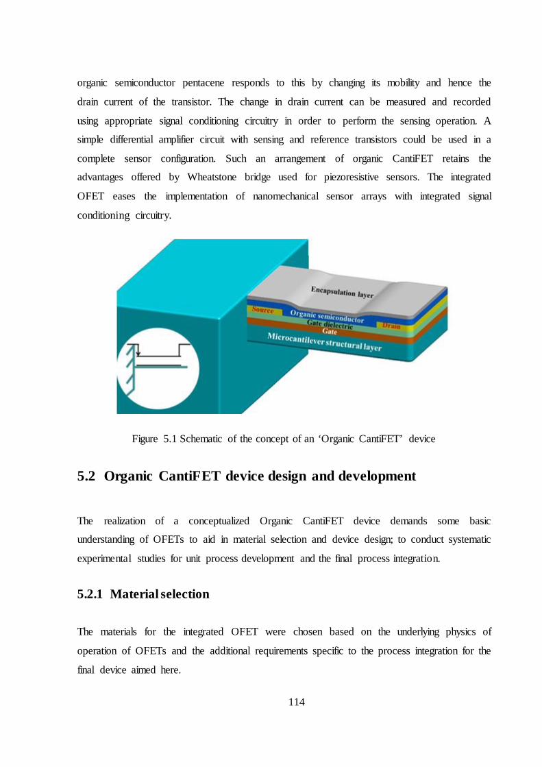
114
organic semiconductor pentacene responds to this by changing its mobility and hence the
drain current of the transistor. The change in drain current can be measured and recorded
using appropriate signal conditioning circuitry in order to perform the sensing operation. A
simple differential amplifier circuit with sensing and reference transistors could be used in a
complete sensor configuration. Such an arrangement of organic CantiFET retains the
advantages offered by Wheatstone bridge used for piezoresistive sensors. The integrated
OFET eases the implementation of nanomechanical sensor arrays with integrated signal
conditioning circuitry.
Figure 5.1 Schematic of the concept of an ‘Organic CantiFET’ device
5.2 Organic CantiFET device design and development
The realization of a conceptualized Organic CantiFET device demands some basic
understanding of OFETs to aid in material selection and device design; to conduct systematic
experimental studies for unit process development and the final process integration.
5.2.1 Material selection
The materials for the integrated OFET were chosen based on the underlying physics of
operation of OFETs and the additional requirements specific to the process integration for the
final device aimed here.
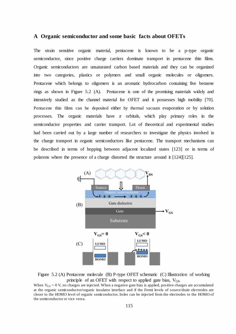
115
A Organic semiconductor and some basic facts about OFETs
The strain sensitive organic material, pentacene is known to be a p-type organic
semiconductor, since positive charge carriers dominate transport in pentacene thin films.
Organic semiconductors are unsaturated carbon based materials and they can be organized
into two categories, plastics or polymers and small organic molecules or oligomers.
Pentacene which belongs to oligomers is an aromatic hydrocarbon containing five benzene
rings as shown in Figure 5.2 (A). Pentacene is one of the promising materials widely and
intensively studied as the channel material for OFET and it possesses high mobility [70].
Pentacene thin films can be deposited either by thermal vacuum evaporation or by solution
processes. The organic materials have π orbitals, which play primary roles in the
semiconductor properties and carrier transport. Lot of theoretical and experimental studies
had been carried out by a large number of researchers to investigate the physics involved in
the charge transport in organic semiconductors like pentacene. The transport mechanisms can
be described in terms of hopping between adjacent localized states [123] or in terms of
polarons where the presence of a charge distorted the structure around it [124][125].
Figure 5.2 (A) Pentacene molecule (B) P-type OFET schematic (C) Illustration of working principle of an OFET with respect to applied gate bias, VGS.
When VGS = 0 V, no charges are injected. When a negative gate bias is applied, positive charges are accumulated at the organic semiconductor/organic insulator interface and if the Fermi levels of source/drain electrodes are closer to the HOMO level of organic semiconductor, holes can be injected from the electrodes to the HOMO of the semiconductor or vice versa.
116
Organic field-effect transistors (OFETs) are 3-terminal devices like MOSFETs in which the
carrier density in the channel region between source and drain can be controlled by the
voltage applied to the third terminal i.e., gate voltage. The schematic of an OFET is shown in
Figure 5.2 (B). The core structure of OFET is the metal insulator semiconductor (MIS)
structure constituted by gate electrode, gate dielectric and the organic semiconductor. The
operating principle of OFET can be imagined similar to that of enhancement MOSFET with a
main difference that OFETs work in accumulation mode whereas MOSFETs work in
inversion mode. The working of an OFET could be described using a simplified energy level
diagram for Fermi level of source/drain electrodes and the energy levels, HOMO (highest
occupied molecular orbital) and LUMO (lowest unoccupied molecular orbital) of the organic
semiconductor. Considering the case where gate voltage is not applied (Figure 5.2 (C)), direct
injection of charge carriers from the source/drain electrodes creates current flow in the
organic semiconductor. Such currents will be relatively small due to high resistance of the
organic semiconductors (the organic semiconductor behaves like an insulator as it is
intrinsically undoped) and large distance between the source and drain electrodes. When a
negative gate voltage is applied (Figure 4b), positive charges are induced or accumulated near
the organic semiconductor/gate dielectric interface to form a p-type conducting channel. If the
Fermi level of source/drain metal is close to the HOMO level of the organic semiconductor,
these positive charges can be extracted by these electrodes by applying appropriate voltage
between these electrodes. The operation of OFETs requires low energetic barriers at the
metal-organic interfaces for both source and drain contacts for proper injection and extraction
of carriers.
Despite the fundamental differences between the modes of operation of OFETs and
MOSFETs, the characteristic equations (eqn. for linear regime and eqn. for saturation regime)
of MOSFET transistors can be applied to the OFETs also [126] as given in equation 5.1 and
5.2.
퐼퐷푠 = μ퐶푂푋
푊퐿
(푉퐺푆 −푉푇퐻)푉퐷푆 −푉퐷푆
2 (5.1)
117
퐼퐷푠 = μ퐶푂푋푊퐿
(푉퐺푆 −푉푇퐻)2 (5.2)
B Source/drain and gate electrodes
In the case of pentacene based OFETS, source and drain regions are not usually doped. So
charge carriers that form the conducting channel of the transistor must get injected from
contacts. The charge injected into the pentacene film depends on the schottky barrier between
the source/ drain metal contacts and the active layer. Thus the charge injection is determined
by the work function of the metal contacts. So for a p-type semiconductor like pentacene, high
work function metals like gold (Au) are commonly used as source/ drain electrodes [127]. The
work function of Au (~5.1 eV)) is closer to the HOMO level of pentacene (~5.2 eV) and
hence reduces the contact resistance. Gate electrode chosen was also Au.
C Gate dielectric
There are a certain number of aspects to be considered for choosing the gate dielectric
material and they include leakage, patterning convenience and compatibility, semiconductor
compatibility, achievable capacitance, hysteresis etc. [127]. The gate dielectric material to be
considered for the organic CantiFET should possess certain qualities other than these basic
qualities required for a good dielectric material for OFETs. To enlist them, the material
should be easily patternable with good process compatibility with SU-8 to and compliance
compatibility with SU-8. Various dielectric materials such as silicon dioxide, HfO2 [126] and
some polymer materials [128][129] are reported to be in use in Pentacene OFETs. Reported
dielectric constant value for Microchem SU-8 2000 series is 4.1 which is close to the value for
silicon dioxide. Hence the feasibility of using SU-8 itself as the dielectric material for
pentacene OFETs was explored.
OFETS with SU-8 as dielectric have been scarcely reported in the literature. A preliminary
study is required in order to analyse the performance of pentacene OFETs with the gate
dielectric made of SU-8 processed in the present laboratory conditions and hence to optimize
the process and layer thickness of SU-8. For this purpose, bottom gate bottom contact
(BGBC) [126] pentacene OFETs were fabricated with different SU-8 dielectric thicknesses
varying from 300 nm to 1µm. The schematic of this BGBC OFET fabrication process
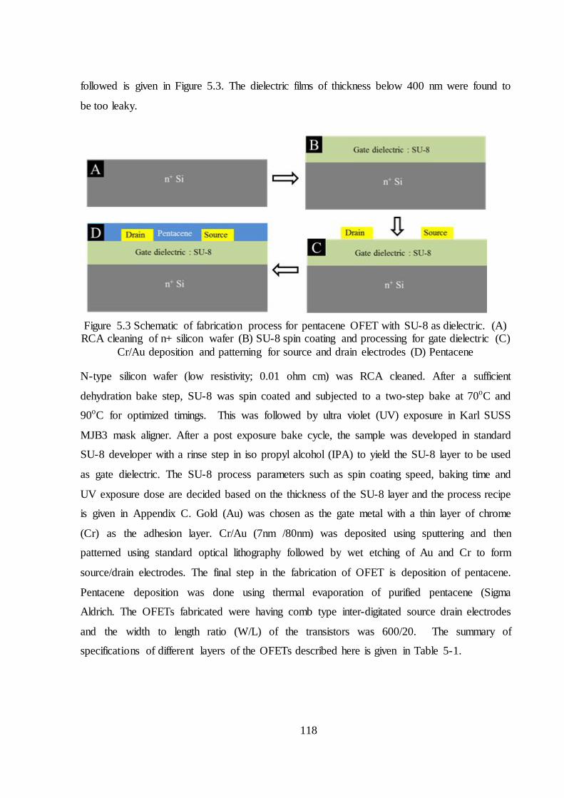
118
followed is given in Figure 5.3. The dielectric films of thickness below 400 nm were found to
be too leaky.
Figure 5.3 Schematic of fabrication process for pentacene OFET with SU-8 as dielectric. (A)
RCA cleaning of n+ silicon wafer (B) SU-8 spin coating and processing for gate dielectric (C) Cr/Au deposition and patterning for source and drain electrodes (D) Pentacene
N-type silicon wafer (low resistivity; 0.01 ohm cm) was RCA cleaned. After a sufficient
dehydration bake step, SU-8 was spin coated and subjected to a two-step bake at 70oC and
90oC for optimized timings. This was followed by ultra violet (UV) exposure in Karl SUSS
MJB3 mask aligner. After a post exposure bake cycle, the sample was developed in standard
SU-8 developer with a rinse step in iso propyl alcohol (IPA) to yield the SU-8 layer to be used
as gate dielectric. The SU-8 process parameters such as spin coating speed, baking time and
UV exposure dose are decided based on the thickness of the SU-8 layer and the process recipe
is given in Appendix C. Gold (Au) was chosen as the gate metal with a thin layer of chrome
(Cr) as the adhesion layer. Cr/Au (7nm /80nm) was deposited using sputtering and then
patterned using standard optical lithography followed by wet etching of Au and Cr to form
source/drain electrodes. The final step in the fabrication of OFET is deposition of pentacene.
Pentacene deposition was done using thermal evaporation of purified pentacene (Sigma
Aldrich. The OFETs fabricated were having comb type inter-digitated source drain electrodes
and the width to length ratio (W/L) of the transistors was 600/20. The summary of
specifications of different layers of the OFETs described here is given in Table 5-1.
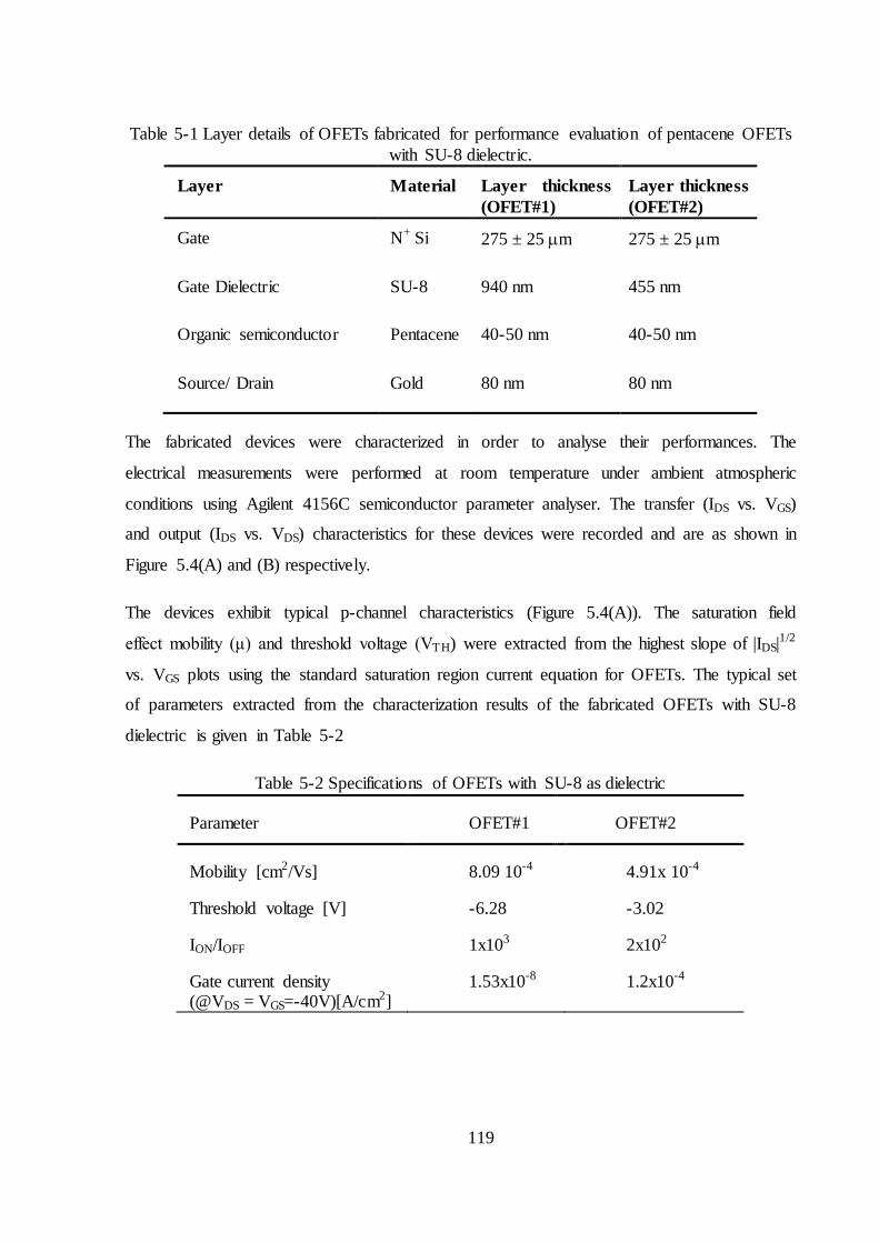
119
Table 5-1 Layer details of OFETs fabricated for performance evaluation of pentacene OFETs with SU-8 dielectric.
Layer Material Layer thickness (OFET#1)
Layer thickness (OFET#2)
Gate N+ Si 275 ± 25 m 275 ± 25 m
Gate Dielectric SU-8 940 nm 455 nm
Organic semiconductor Pentacene 40-50 nm 40-50 nm
Source/ Drain Gold 80 nm 80 nm
The fabricated devices were characterized in order to analyse their performances. The
electrical measurements were performed at room temperature under ambient atmospheric
conditions using Agilent 4156C semiconductor parameter analyser. The transfer (IDS vs. VGS)
and output (IDS vs. VDS) characteristics for these devices were recorded and are as shown in
Figure 5.4(A) and (B) respectively.
The devices exhibit typical p-channel characteristics (Figure 5.4(A)). The saturation field
effect mobility (μ) and threshold voltage (VTH) were extracted from the highest slope of |IDS|1/2
vs. VGS plots using the standard saturation region current equation for OFETs. The typical set
of parameters extracted from the characterization results of the fabricated OFETs with SU-8
dielectric is given in Table 5-2
Table 5-2 Specifications of OFETs with SU-8 as dielectric
Parameter OFET#1 OFET#2
Mobility [cm2/Vs] 8.09 10-4 4.91x 10⁻⁴
Threshold voltage [V] -6.28 -3.02
ION/IOFF 1x10³ 2x10²
Gate current density (@VDS = VGS=-40V)[A/cm2]
1.53x10⁻⁸ 1.2x10⁻⁴
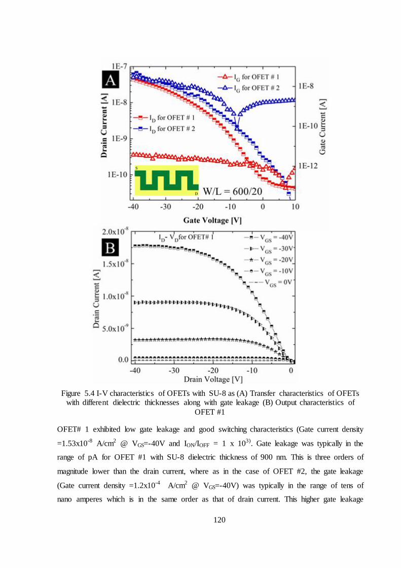
120
Figure 5.4 I-V characteristics of OFETs with SU-8 as (A) Transfer characteristics of OFETs
with different dielectric thicknesses along with gate leakage (B) Output characteristics of OFET #1
OFET# 1 exhibited low gate leakage and good switching characteristics (Gate current density
=1.53x10⁻⁸ A/cm2 @ VGS=-40V and ION/IOFF = 1 x 10³). Gate leakage was typically in the
range of pA for OFET #1 with SU-8 dielectric thickness of 900 nm. This is three orders of
magnitude lower than the drain current, where as in the case of OFET #2, the gate leakage
(Gate current density =1.2x10⁻⁴ A/cm2 @ VGS=-40V) was typically in the range of tens of
nano amperes which is in the same order as that of drain current. This higher gate leakage
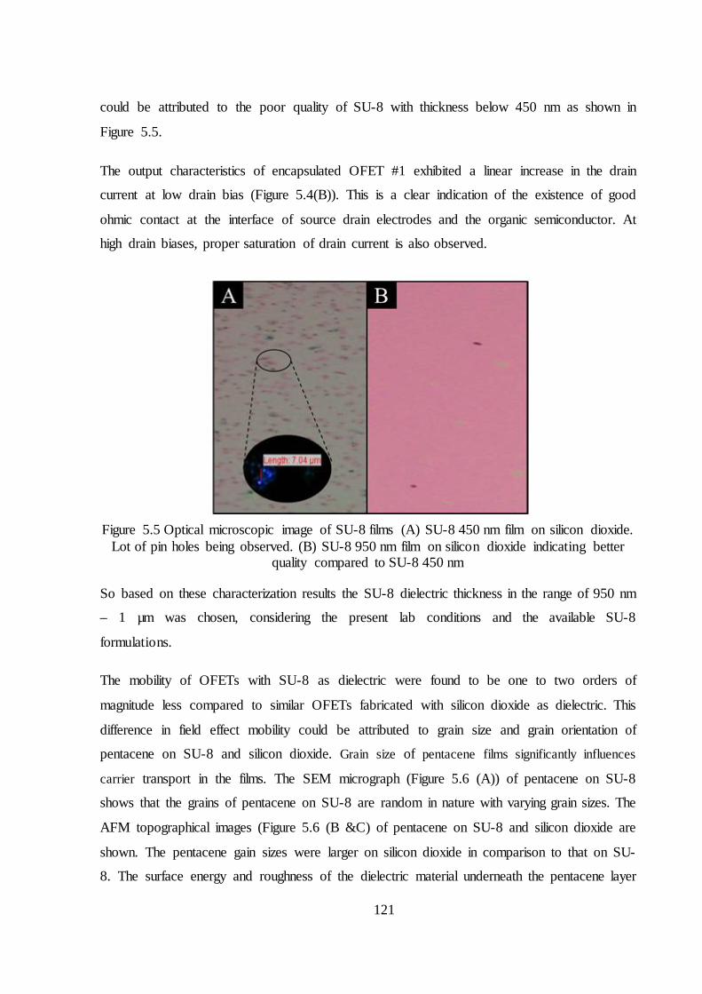
121
could be attributed to the poor quality of SU-8 with thickness below 450 nm as shown in
Figure 5.5.
The output characteristics of encapsulated OFET #1 exhibited a linear increase in the drain
current at low drain bias (Figure 5.4(B)). This is a clear indication of the existence of good
ohmic contact at the interface of source drain electrodes and the organic semiconductor. At
high drain biases, proper saturation of drain current is also observed.
Figure 5.5 Optical microscopic image of SU-8 films (A) SU-8 450 nm film on silicon dioxide.
Lot of pin holes being observed. (B) SU-8 950 nm film on silicon dioxide indicating better quality compared to SU-8 450 nm
So based on these characterization results the SU-8 dielectric thickness in the range of 950 nm
– 1 µm was chosen, considering the present lab conditions and the available SU-8
formulations.
The mobility of OFETs with SU-8 as dielectric were found to be one to two orders of
magnitude less compared to similar OFETs fabricated with silicon dioxide as dielectric. This
difference in field effect mobility could be attributed to grain size and grain orientation of
pentacene on SU-8 and silicon dioxide. Grain size of pentacene films significantly influences
carrier transport in the films. The SEM micrograph (Figure 5.6 (A)) of pentacene on SU-8
shows that the grains of pentacene on SU-8 are random in nature with varying grain sizes. The
AFM topographical images (Figure 5.6 (B &C) of pentacene on SU-8 and silicon dioxide are
shown. The pentacene gain sizes were larger on silicon dioxide in comparison to that on SU-
8. The surface energy and roughness of the dielectric material underneath the pentacene layer
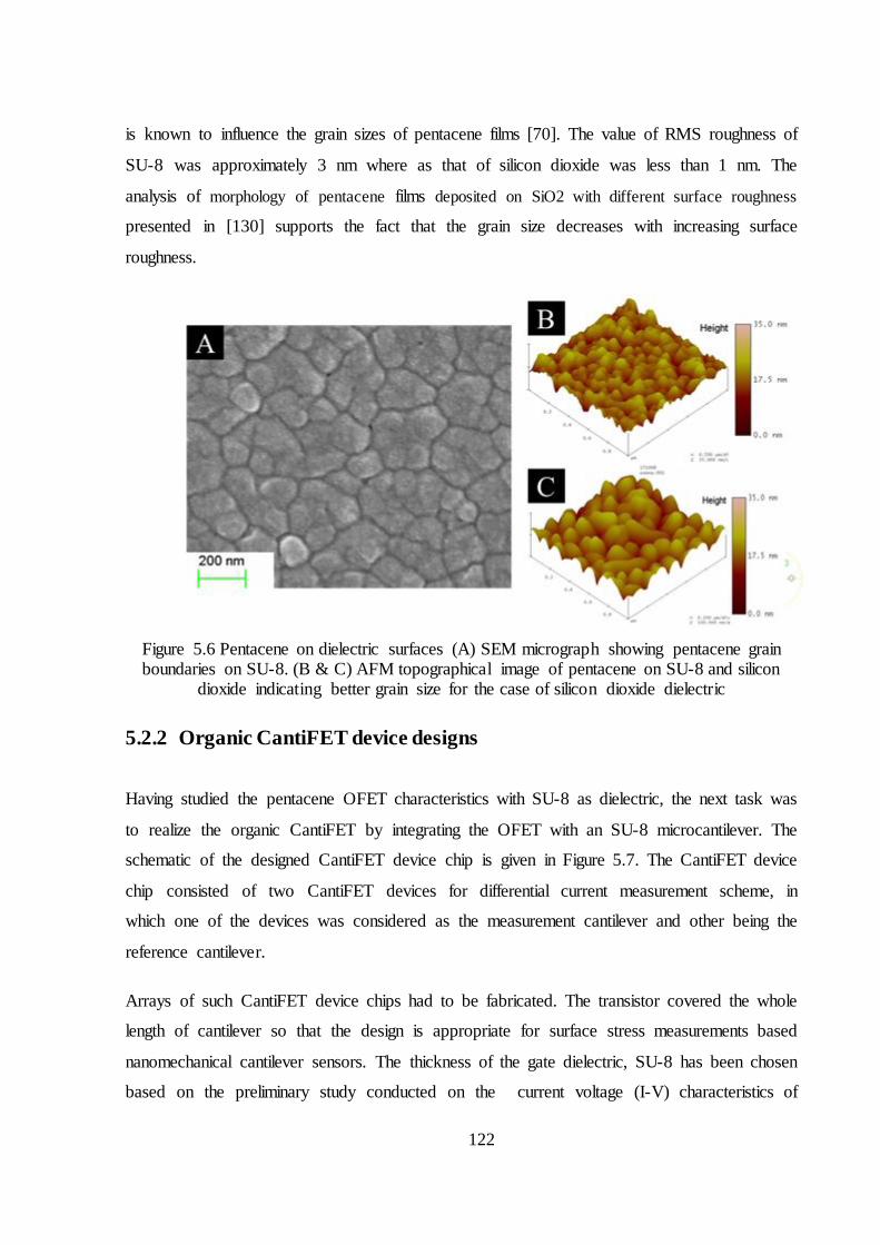
122
is known to influence the grain sizes of pentacene films [70]. The value of RMS roughness of
SU-8 was approximately 3 nm where as that of silicon dioxide was less than 1 nm. The
analysis of morphology of pentacene films deposited on SiO2 with different surface roughness
presented in [130] supports the fact that the grain size decreases with increasing surface
roughness.
Figure 5.6 Pentacene on dielectric surfaces (A) SEM micrograph showing pentacene grain boundaries on SU-8. (B & C) AFM topographical image of pentacene on SU-8 and silicon
dioxide indicating better grain size for the case of silicon dioxide dielectric
5.2.2 Organic CantiFET device designs
Having studied the pentacene OFET characteristics with SU-8 as dielectric, the next task was
to realize the organic CantiFET by integrating the OFET with an SU-8 microcantilever. The
schematic of the designed CantiFET device chip is given in Figure 5.7. The CantiFET device
chip consisted of two CantiFET devices for differential current measurement scheme, in
which one of the devices was considered as the measurement cantilever and other being the
reference cantilever.
Arrays of such CantiFET device chips had to be fabricated. The transistor covered the whole
length of cantilever so that the design is appropriate for surface stress measurements based
nanomechanical cantilever sensors. The thickness of the gate dielectric, SU-8 has been chosen
based on the preliminary study conducted on the current voltage (I-V) characteristics of
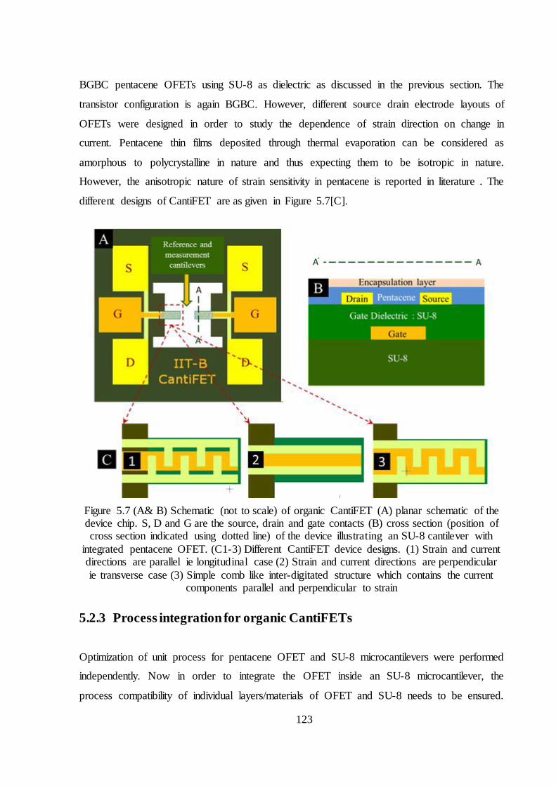
123
BGBC pentacene OFETs using SU-8 as dielectric as discussed in the previous section. The
transistor configuration is again BGBC. However, different source drain electrode layouts of
OFETs were designed in order to study the dependence of strain direction on change in
current. Pentacene thin films deposited through thermal evaporation can be considered as
amorphous to polycrystalline in nature and thus expecting them to be isotropic in nature.
However, the anisotropic nature of strain sensitivity in pentacene is reported in literature . The
different designs of CantiFET are as given in Figure 5.7[C].
Figure 5.7 (A& B) Schematic (not to scale) of organic CantiFET (A) planar schematic of the device chip. S, D and G are the source, drain and gate contacts (B) cross section (position of cross section indicated using dotted line) of the device illustrating an SU-8 cantilever with
integrated pentacene OFET. (C1-3) Different CantiFET device designs. (1) Strain and current directions are parallel ie longitudinal case (2) Strain and current directions are perpendicular ie transverse case (3) Simple comb like inter-digitated structure which contains the current
components parallel and perpendicular to strain
5.2.3 Process integration for organic CantiFETs
Optimization of unit process for pentacene OFET and SU-8 microcantilevers were performed
independently. Now in order to integrate the OFET inside an SU-8 microcantilever, the
process compatibility of individual layers/materials of OFET and SU-8 needs to be ensured.

124
The process integration of organic FET with solution processed polymer materials like SU-8
is a real challenge as the organic semiconductor, pentacene is known to get degraded by
organic solvents. Effect of SU-8 or its solvent cyclopentanone and developer PGMEA on
pentacene is not yet reported. So simple and quick test experiments were conducted in which
pentacene OFETs were fabricated and characterized. SU-8 was spin coated and then removed
immediately using PGMEA developer. Then the transistor was characterized and it was found
that the OFET did not show transistor behaviour and this is clear indication that pentacene
semiconductor was degraded in exposure to SU-8 or its developer. In order to separate the
two effects one more set of experiments were conducted in which the pentacene OFET was
dipped inside the solvent for SU-8 ie, cyclopentanone and then dried and the transistor was
characterized. OFET in this case also did not work. With these two sets of experiments, it
became clear that SU-8 and SU-8 developer would degrade the pentacene layer and hence the
process integration of OFET with SU-8 cantilever needs to be planned to avoid the exposure
of pentacene layer to organic solvents used in SU-8 lithography.
For this, a novel, yet simple process sequence is followed, in which, one develops all the
required layers except the pentacene layer for OFET on the SU-8 cantilever and then deposits
pentacene layer after the releasing the device chips from the substrate to form the final
organic cantiFET. This process has inherent advantages such as (1) this avoids the exposure
of pentacene layer to organic solvents used in SU-8 lithography (2) obviates the need for
patterning of pentacene layer which is known to be a difficult task. The schematic of this
fabrication sequence is given in figure and process steps are detailed as below. The process
recipe followed while fabricating organic CantiFET and the design of mask sets are given in
Appendix C and Appendix D respectively.
Step 1: Release/Sacrificial Layer
An RCA /Pirahna cleaned silicon wafer that was used as a reusable dummy substrate. The
first layer to be developed was sacrificial layer used as the release layer for separating out the
polymer cantiFET chips from the dummy substrate. The sacrificial layer chosen here was
silicon dioxide layer (sputtered oxide with thickness more than 200 nm or thermally grown
silicon dioxide with thickness = 700 nm to 800 nm) and the arguments for choosing this
material remains the same as described in Chapter 2 and Chapter 3.
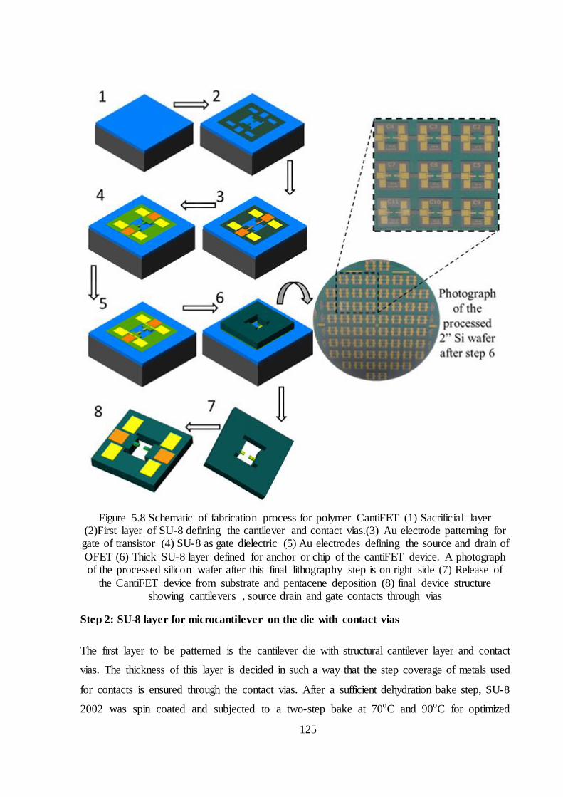
125
Figure 5.8 Schematic of fabrication process for polymer CantiFET (1) Sacrificial layer
(2)First layer of SU-8 defining the cantilever and contact vias.(3) Au electrode patterning for gate of transistor (4) SU-8 as gate dielectric (5) Au electrodes defining the source and drain of OFET (6) Thick SU-8 layer defined for anchor or chip of the cantiFET device. A photograph of the processed silicon wafer after this final lithography step is on right side (7) Release of
the CantiFET device from substrate and pentacene deposition (8) final device structure showing cantilevers , source drain and gate contacts through vias
Step 2: SU-8 layer for microcantilever on the die with contact vias
The first layer to be patterned is the cantilever die with structural cantilever layer and contact
vias. The thickness of this layer is decided in such a way that the step coverage of metals used
for contacts is ensured through the contact vias. After a sufficient dehydration bake step, SU-8
2002 was spin coated and subjected to a two-step bake at 70oC and 90oC for optimized
126
timings with a slow ramp up and ramp down to reduce the stress in structural layer. This was
followed by ultra violet (UV) exposure in Karl SUSS MJB3 mask aligner using the respective
mask (Mask#1). After a post exposure bake cycle, the sample was developed in standard SU-
8 developer with a rinse step in iso propyl alcohol (IPA) to yield the first SU-8 layer as shown
in step 2 of Figure 5.8. This layer was subjected to a post development baking step (hard bake
at low temperature) in order to improve the stability of the layer and to remove built-in
thermal stress developed if any.
Step 3: Gate electrode and contact pads for integrated OFET
Gate electrode and contact pads of the OFET are defined using gold (Au). Au was chosen as
the gate metal with a thin layer of chrome (Cr) as the adhesion layer. Cr/Au (7nm /80nm) was
deposited using sputtering and then patterned using standard optical lithography (Mask #2)
followed by wet etching of Au and Cr to form the gate electrode and contact pads as given in
in step 3 of Figure 5.8.
Step 4: Gate dielectric (SU-8)
Gate dielectric of the OFET is defined using SU-8 2002. The process as well as the mask is
very similar to the first SU-8 layer (mask used was Mask #1).
Step 5: Source and drain electrodes and contact pads
Cr/Au layers were sputter deposited and patterned using the respective mask (Mask #3) for
the formation of source, drain electrodes and the contacts, by following the same process
recipe for gate electrode/contacts.
Step 6: Anchor or polymer device die
A thick SU-8 layer of thickness more than 100 microns is to be patterned to form the anchor
or the device chip and the frames for holding arrays of device chips for ease in handling. For
this SU-8 2100 is spin coated followed by a two-step baking process on a hot plate at
temperatures 65oC and 85oC and subsequent lithography steps using an optimized process
recipe for 150 micron thick SU-8. Photograph of a processed 2” silicon wafer after the final
lithography step (in step 6 of Figure 5.8) is also shown in Figure 5.8, where arrays of SU-8
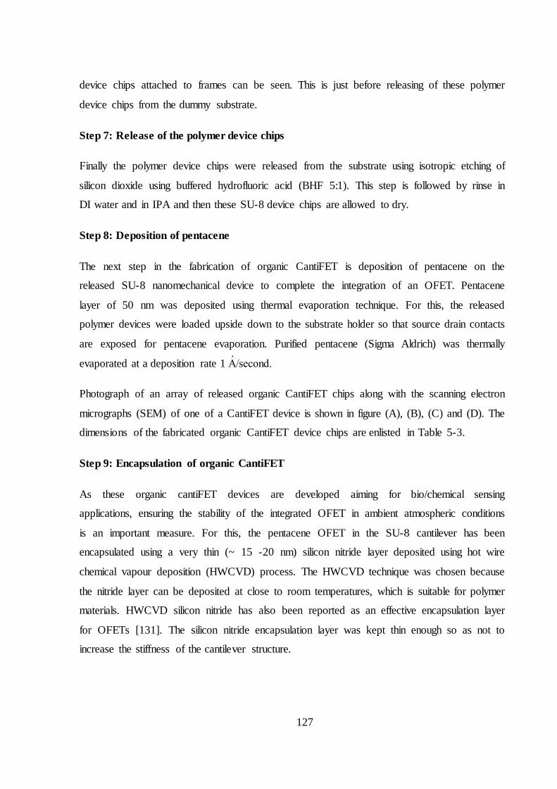
127
device chips attached to frames can be seen. This is just before releasing of these polymer
device chips from the dummy substrate.
Step 7: Release of the polymer device chips
Finally the polymer device chips were released from the substrate using isotropic etching of
silicon dioxide using buffered hydrofluoric acid (BHF 5:1). This step is followed by rinse in
DI water and in IPA and then these SU-8 device chips are allowed to dry.
Step 8: Deposition of pentacene
The next step in the fabrication of organic CantiFET is deposition of pentacene on the
released SU-8 nanomechanical device to complete the integration of an OFET. Pentacene
layer of 50 nm was deposited using thermal evaporation technique. For this, the released
polymer devices were loaded upside down to the substrate holder so that source drain contacts
are exposed for pentacene evaporation. Purified pentacene (Sigma Aldrich) was thermally
evaporated at a deposition rate 1 Ǻ/second.
Photograph of an array of released organic CantiFET chips along with the scanning electron
micrographs (SEM) of one of a CantiFET device is shown in figure (A), (B), (C) and (D). The
dimensions of the fabricated organic CantiFET device chips are enlisted in Table 5-3.
Step 9: Encapsulation of organic CantiFET
As these organic cantiFET devices are developed aiming for bio/chemical sensing
applications, ensuring the stability of the integrated OFET in ambient atmospheric conditions
is an important measure. For this, the pentacene OFET in the SU-8 cantilever has been
encapsulated using a very thin (~ 15 -20 nm) silicon nitride layer deposited using hot wire
chemical vapour deposition (HWCVD) process. The HWCVD technique was chosen because
the nitride layer can be deposited at close to room temperatures, which is suitable for polymer
materials. HWCVD silicon nitride has also been reported as an effective encapsulation layer
for OFETs [131]. The silicon nitride encapsulation layer was kept thin enough so as not to
increase the stiffness of the cantilever structure.

128
Figure 5.9 (A) Photographs of released arrays of organic CantiFETs (B) SEM micrograph of
the fabricated CantiFET device (C) Bottom and enlarged view of cantilever portion of the CantiFET from SEM showing the inter digitated source drain electrode configuration (Type 1 & 3 CantiFET) (D) Top and enlarged view of cantilever portion of the CantiFET from SEM
Table 5-3 Specifications of organic CantiFET device chips
Property CantiFET#1
(Unit : µm)
CantiFET#2
(Unit : µm)
CantiFET#3
(Unit : µm)
Cantilever length 312 312 312
Cantilever width 168 168 168
Cantilever thickness 2 2 2
SU-8 dielectric thickness 0.95 0.95 0.95
OFET W/L 300/17 300/27 523/17
Pentacene thickness
Silicon nitride encapsulation
0.05
0.015
0.05
0.015
0.05
0.015
CantiFET chip area 4000 x 4000 4000 x 4000 4000 x 4000
5.3 Characterization of Organic CantiFET
The as-fabricated organic CantiFET devices were systematically characterized with respect to
their electrical, mechanical and electromechanical and noise parameters.
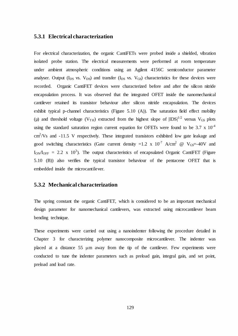
129
5.3.1 Electrical characterization
For electrical characterization, the organic CantiFETs were probed inside a shielded, vibration
isolated probe station. The electrical measurements were performed at room temperature
under ambient atmospheric conditions using an Agilent 4156C semiconductor parameter
analyser. Output (IDS vs. VDS) and transfer (IDS vs. VGS) characteristics for these devices were
recorded. Organic CantiFET devices were characterized before and after the silicon nitride
encapsulation process. It was observed that the integrated OFET inside the nanomechanical
cantilever retained its transistor behaviour after silicon nitride encapsulation. The devices
exhibit typical p-channel characteristics (Figure 5.10 (A)). The saturation field effect mobility
(µ) and threshold voltage (VTH) extracted from the highest slope of |IDS|1/2 versus VGS plots
using the standard saturation region current equation for OFETs were found to be 3.7 x 10⁻⁴
cm2/Vs and -11.5 V respectively. These integrated transistors exhibited low gate leakage and
good switching characteristics (Gate current density =1.2 x 10⁻⁷ A/cm2 @ VGS=-40V and
ION/IOFF = 2.2 x 10³). The output characteristics of encapsulated Organic CantiFET (Figure
5.10 (B)) also verifies the typical transistor behaviour of the pentacene OFET that is
embedded inside the microcantilever.
5.3.2 Mechanical characterization
The spring constant the organic CantiFET, which is considered to be an important mechanical
design parameter for nanomechanical cantilevers, was extracted using microcantilever beam
bending technique.
These experiments were carried out using a nanoindenter following the procedure detailed in
Chapter 3 for characterizing polymer nanocomposite microcantilever. The indenter was
placed at a distance 55 m away from the tip of the cantilever. Few experiments were
conducted to tune the indenter parameters such as preload gain, integral gain, and set point,
preload and load rate.
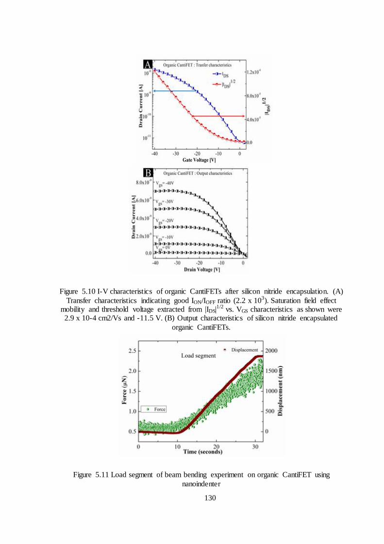
130
Figure 5.10 I-V characteristics of organic CantiFETs after silicon nitride encapsulation. (A) Transfer characteristics indicating good ION/IOFF ratio (2.2 x 10³). Saturation field effect
mobility and threshold voltage extracted from |IDS|1/2 vs. VGS characteristics as shown were 2.9 x 10⁻⁴ cm2/Vs and -11.5 V. (B) Output characteristics of silicon nitride encapsulated
organic CantiFETs.
Figure 5.11 Load segment of beam bending experiment on organic CantiFET using nanoindenter
131
The load segment showing the load and displacement as a function of time for the optimized
load rate is shown in Figure 5.11. The load vs. displacement curve for the CantiFET structure
can be plotted as given in Figure 5.12, with the slope being 0.6 N/m. The actual spring
constant of the cantilever structure was calculated from the slope of the curve using equation
given in the graph. Here L is the length of the cantilever structure, l is the distance from the
tip of the cantilever where indenter tip is placed as indicated in the inset of the plot. The
spring constant obtained using this method was 0.4 N/m.
Figure 5.12 Load displacement characteristics of Organic CantiFET. Inset showing the optical
micrograph of the image indicating the location of indenter placement.
From this the resonance frequency was calculated using the equation (equation 5.3) used for
first mode of vibration of rectangular microcantilever beams
*
12res
kfm
(5.3)
where k is the spring constant and m* is the effective mass of the microcantilever. Here the
value of the spring constant obtained from previous beam bending technique (0.4 N/m) was
used. The effective mass was calculated considering the layers of SU-8 and gold. Given the
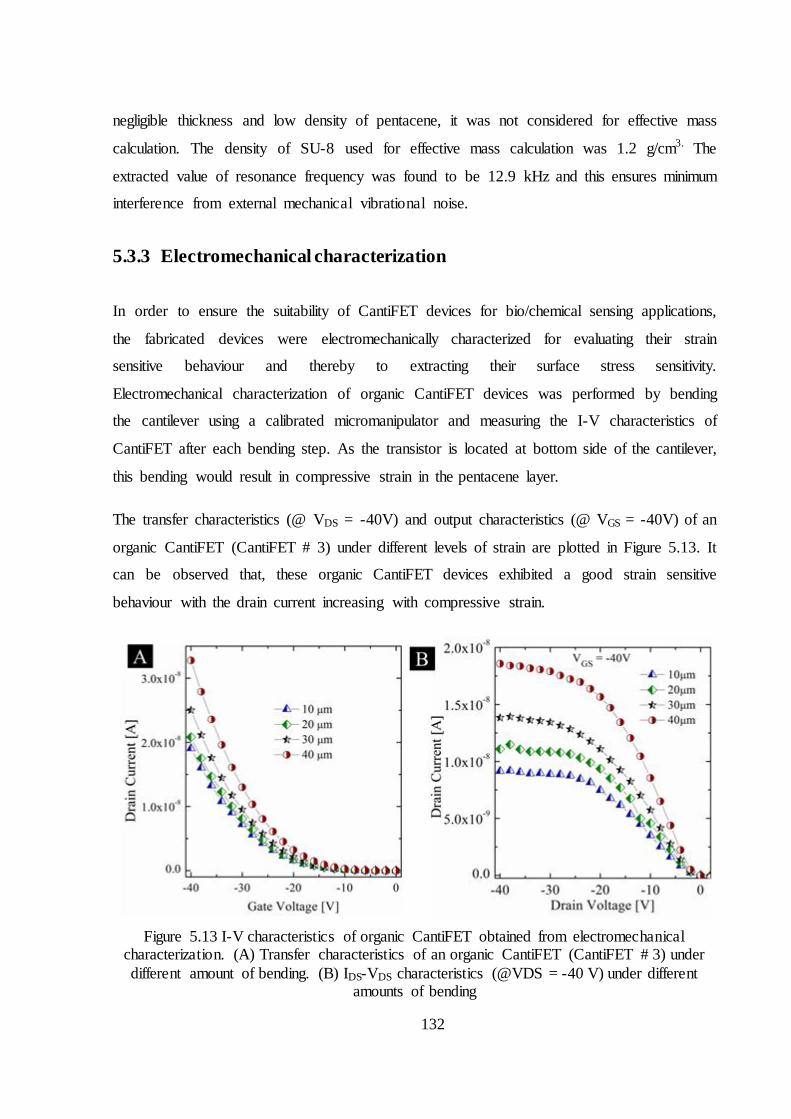
132
negligible thickness and low density of pentacene, it was not considered for effective mass
calculation. The density of SU-8 used for effective mass calculation was 1.2 g/cm3. The
extracted value of resonance frequency was found to be 12.9 kHz and this ensures minimum
interference from external mechanical vibrational noise.
5.3.3 Electromechanical characterization
In order to ensure the suitability of CantiFET devices for bio/chemical sensing applications,
the fabricated devices were electromechanically characterized for evaluating their strain
sensitive behaviour and thereby to extracting their surface stress sensitivity.
Electromechanical characterization of organic CantiFET devices was performed by bending
the cantilever using a calibrated micromanipulator and measuring the I-V characteristics of
CantiFET after each bending step. As the transistor is located at bottom side of the cantilever,
this bending would result in compressive strain in the pentacene layer.
The transfer characteristics (@ VDS = -40V) and output characteristics (@ VGS = -40V) of an
organic CantiFET (CantiFET # 3) under different levels of strain are plotted in Figure 5.13. It
can be observed that, these organic CantiFET devices exhibited a good strain sensitive
behaviour with the drain current increasing with compressive strain.
Figure 5.13 I-V characteristics of organic CantiFET obtained from electromechanical
characterization. (A) Transfer characteristics of an organic CantiFET (CantiFET # 3) under different amount of bending. (B) IDS-VDS characteristics (@VDS = -40 V) under different
amounts of bending
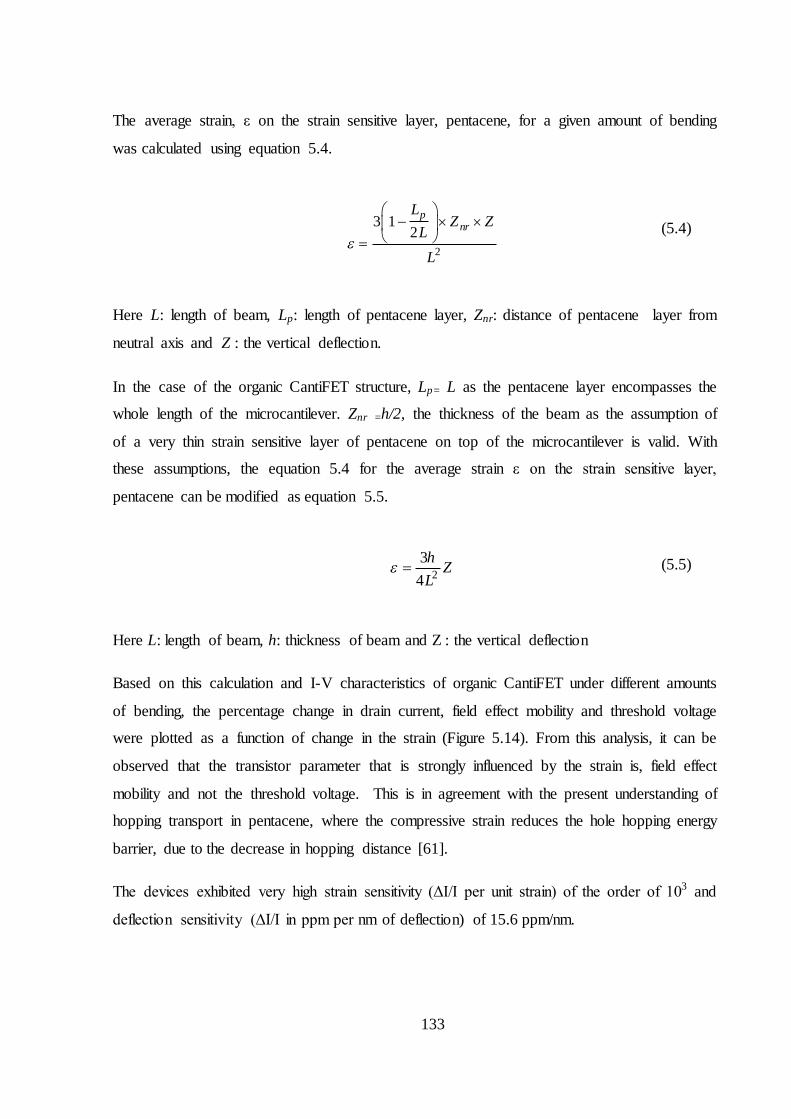
133
The average strain, ε on the strain sensitive layer, pentacene, for a given amount of bending
was calculated using equation 5.4.
2
3 12
pnr
LZ Z
LL
(5.4)
Here L: length of beam, Lp: length of pentacene layer, Znr: distance of pentacene layer from
neutral axis and Z : the vertical deflection.
In the case of the organic CantiFET structure, Lp= L as the pentacene layer encompasses the
whole length of the microcantilever. Znr =h/2, the thickness of the beam as the assumption of
of a very thin strain sensitive layer of pentacene on top of the microcantilever is valid. With
these assumptions, the equation 5.4 for the average strain ε on the strain sensitive layer,
pentacene can be modified as equation 5.5.
2
34
h ZL
(5.5)
Here L: length of beam, h: thickness of beam and Z : the vertical deflection
Based on this calculation and I-V characteristics of organic CantiFET under different amounts
of bending, the percentage change in drain current, field effect mobility and threshold voltage
were plotted as a function of change in the strain (Figure 5.14). From this analysis, it can be
observed that the transistor parameter that is strongly influenced by the strain is, field effect
mobility and not the threshold voltage. This is in agreement with the present understanding of
hopping transport in pentacene, where the compressive strain reduces the hole hopping energy
barrier, due to the decrease in hopping distance [61].
The devices exhibited very high strain sensitivity (ΔI/I per unit strain) of the order of 103 and
deflection sensitivity (ΔI/I in ppm per nm of deflection) of 15.6 ppm/nm.
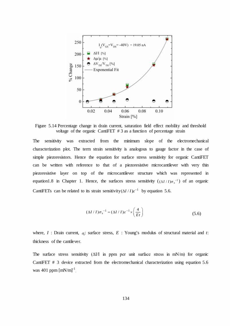
134
Figure 5.14 Percentage change in drain current, saturation field effect mobility and threshold
voltage of the organic CantiFET # 3 as a function of percentage strain
The sensitivity was extracted from the minimum slope of the electromechanical
characterization plot. The term strain sensitivity is analogous to gauge factor in the case of
simple piezoresistors. Hence the equation for surface stress sensitivity for organic CantiFET
can be written with reference to that of a piezoresistive microcantilever with very thin
piezoresistive layer on top of the microcantilever structure which was represented in
equation1.8 in Chapter 1. Hence, the surfaces stress sensitivity ( 1( / ) sI I ) of an organic
CantiFETs can be related to its strain sensitivity 1( / )I I by equation 5.6.
1 1 4( / ) ( / )sI I I IE t
(5.6)
where, I : Drain current, s : surface stress, E : Young’s modulus of structural material and t:
thickness of the cantilever.
The surface stress sensitivity (ΔI/I in ppm per unit surface stress in mN/m) for organic
CantiFET # 3 device extracted from the electromechanical characterization using equation 5.6
was 401 ppm [mN/m]-1.
135
Figure 5.15 Percentage change in drain of as a function of percentage strain (A) CantiFET # 1
The average value of Idsat at strain %= 0 was 11 nA (B) CantiFET # 2. The average value of Idsat at strain %= 0 was 6 nA
Other two types of organic CantiFET devices were also characterized for evaluating their
strain sensitive behaviours. The characterization method and the extraction of parameters
remains the same. The percentage change in drain current as a function of strain for CantiFET
#1 and CantiFET #2 are given in Figure 5.15. It was observed that, CantiFET #1 devices
showed increase in drain current with compressive strain (Figure 5.15 (A)). But CantiFET #2
devices did not show any clear trend in their strain sensitivity behaviour as is illustrated in
Figure 5.15 (B).
Organic CantiFET # 1 and CantiFET # 3 exhibited similar levels of strain sensitivity. So a set
of devices of CantiFET # 1 and CantiFET # 3 were fabricated and characterized together to
investigate the device variability pertaining to strain sensitivity. A plot of mean and standard
deviation of percentage change in current as a function of strain is shown in Figure 5.16. The
standard deviation in sensitivity was found to be within 40 %.
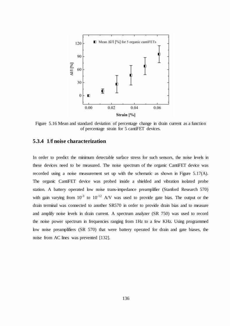
136
Figure 5.16 Mean and standard deviation of percentage change in drain current as a function
of percentage strain for 5 cantiFET devices.
5.3.4 1/f noise characterization
In order to predict the minimum detectable surface stress for such sensors, the noise levels in
these devices need to be measured. The noise spectrum of the organic CantiFET device was
recorded using a noise measurement set up with the schematic as shown in Figure 5.17(A).
The organic CantiFET device was probed inside a shielded and vibration isolated probe
station. A battery operated low noise trans-impedance preamplifier (Stanford Research 570)
with gain varying from 10-3 to 10-12 A/V was used to provide gate bias. The output or the
drain terminal was connected to another SR570 in order to provide drain bias and to measure
and amplify noise levels in drain current. A spectrum analyzer (SR 750) was used to record
the noise power spectrum in frequencies ranging from 1Hz to a few KHz. Using programmed
low noise preamplifiers (SR 570) that were battery operated for drain and gate biases, the
noise from AC lines was prevented [132].
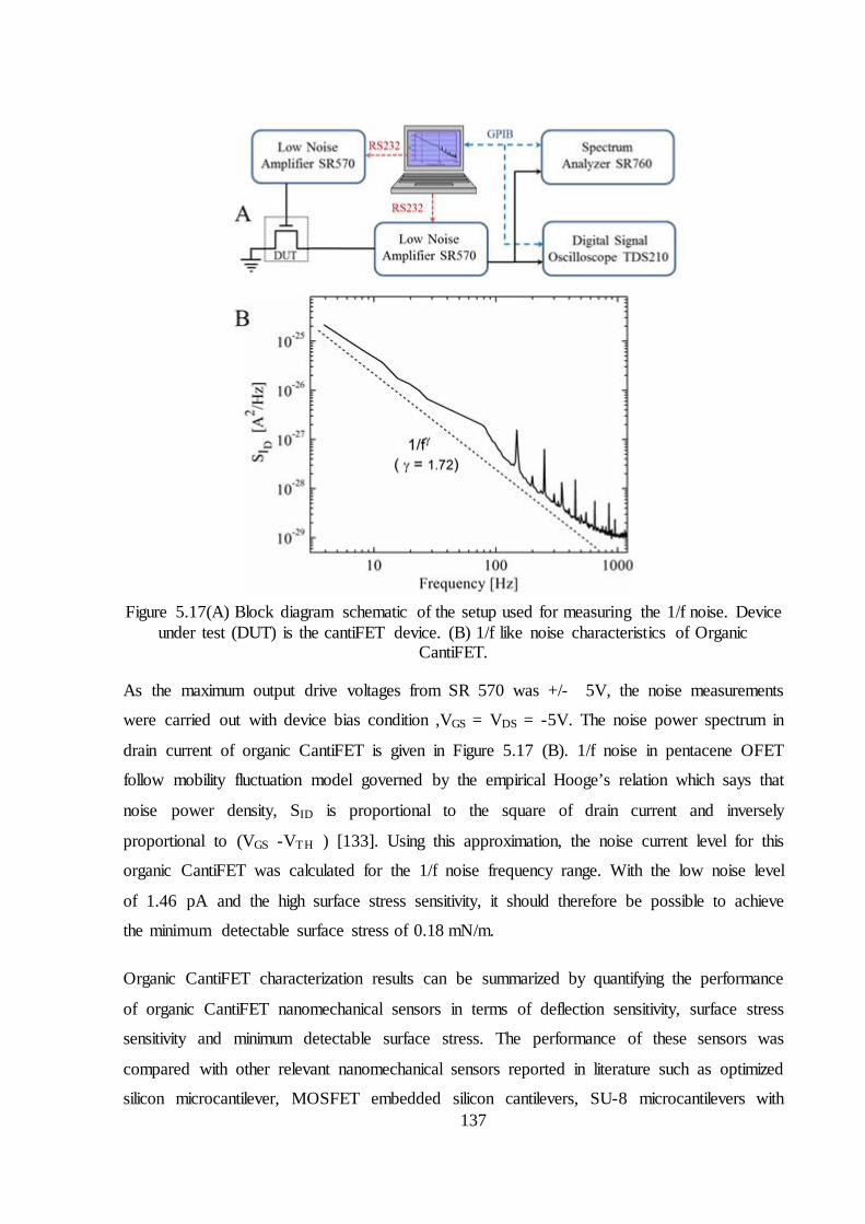
137
Figure 5.17(A) Block diagram schematic of the setup used for measuring the 1/f noise. Device
under test (DUT) is the cantiFET device. (B) 1/f like noise characteristics of Organic CantiFET.
As the maximum output drive voltages from SR 570 was +/- 5V, the noise measurements
were carried out with device bias condition ,VGS = VDS = -5V. The noise power spectrum in
drain current of organic CantiFET is given in Figure 5.17 (B). 1/f noise in pentacene OFET
follow mobility fluctuation model governed by the empirical Hooge’s relation which says that
noise power density, SID is proportional to the square of drain current and inversely
proportional to (VGS -VTH ) [133]. Using this approximation, the noise current level for this
organic CantiFET was calculated for the 1/f noise frequency range. With the low noise level
of 1.46 pA and the high surface stress sensitivity, it should therefore be possible to achieve
the minimum detectable surface stress of 0.18 mN/m.
Organic CantiFET characterization results can be summarized by quantifying the performance
of organic CantiFET nanomechanical sensors in terms of deflection sensitivity, surface stress
sensitivity and minimum detectable surface stress. The performance of these sensors was
compared with other relevant nanomechanical sensors reported in literature such as optimized
silicon microcantilever, MOSFET embedded silicon cantilevers, SU-8 microcantilevers with
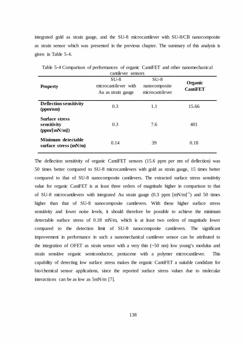
138
integrated gold as strain gauge, and the SU-8 microcantilever with SU-8/CB nanocomposite
as strain sensor which was presented in the previous chapter. The summary of this analysis is
given in Table 5-4.
Table 5-4 Comparison of performances of organic CantiFET and other nanomechanical cantilever sensors
Property SU-8
microcantilever with Au as strain gauge
SU-8 nanocomposite microcantilever
Organic CantiFET
Deflection sensitivity (ppm/nm) 0.3 1.1 15.66
Surface stress sensitivity (ppm/[mN/m])
0.3 7.6 401
Minimum detectable surface stress (mN/m) 0.14 39 0.18
The deflection sensitivity of organic CantiFET sensors (15.6 ppm per nm of deflection) was
50 times better compared to SU-8 microcantilevers with gold as strain gauge, 15 times better
compared to that of SU-8 nanocomposite cantilevers. The extracted surface stress sensitivity
value for organic CaniFET is at least three orders of magnitude higher in comparison to that
of SU-8 microcantilevers with integrated Au strain gauge (0.3 ppm [mN/m]-1) and 50 times
higher than that of SU-8 nanocomposite cantilevers. With these higher surface stress
sensitivity and lower noise levels, it should therefore be possible to achieve the minimum
detectable surface stress of 0.18 mN/m, which is at least two orders of magnitude lower
compared to the detection limit of SU-8 nanocomposite cantilevers. The significant
improvement in performance in such a nanomechanical cantilever sensor can be attributed to
the integration of OFET as strain sensor with a very thin (~50 nm) low young’s modulus and
strain sensitive organic semiconductor, pentacene with a polymer microcantilever. This
capability of detecting low surface stress makes the organic CantiFET a suitable candidate for
bio/chemical sensor applications, since the reported surface stress values due to molecular
interactions can be as low as 5mN/m [7].
139
5.4 Summary
In summary, polymer nanomechanical cantilever sensors with a novel electrical transduction
scheme by integrating a strain sensitive pentacene OFET inside an SU-8 cantilever have been
explored. This novel device was named as ‘Organic CantiFET’. The ways of integrating the
pentacene OFET with an SU-8 microcantilever were explored by evaluating the performance
of OFET with SU-8 dielectric and by analysing process compatibility for fabricating these
two devices (OFET and SU-8 microcantilever). With optimizations at the unit process level,
organic CantiFET devices with different configurations were designed and fabricated. The
fabrication process followed is a novel yet simple process that avoided the exposure of
pentacene to organic solvents used in SU-8 processing with an additional benefit of omitting
the patterning step of the pentacene layer. These devices have been subsequently
characterized for their mechanical, electrical, electromechanical and noise characteristics and
thereby evaluating their performance parameters. It has been observed that these devices
exhibit a very high deflection sensitivity (15.6 ppm/nm) and their surface stress sensitivity
(401 ppm [mN/m]-1) is at least 50 times higher as compared to that of a polymer
nanocomposite cantilever while the lower limit surface stress detection is in the range of 0.18
mN/m. The cost of fabrication of such polymer devices is typically much lower than the
conventional silicon based microcantilevers. Because of these advantages, organic CantiFETs
could pave the way for development of low cost and highly sensitive bio/chemical sensors for
a variety of applications. Further, the concept of integrating a strain sensitive OFET on a
suspended polymer structure can open up new avenues for realizing ultra-sensitive strain
sensors for pressure and inertial sensing applications.
140
Chapter 6
Conclusion and future recommendations
SU-8 nanomechanical cantilever sensors with two efficient electrical transduction schemes
have been successfully developed. The highlights of the major contributions from this
research work discussed in various chapters are enlisted below:-
[1] Design and fabrication of polymer nanocomposite (SU-8/CB) microcantilevers with
overall stack thickness of just 3 µm. The deflection sensitivity of these cantilevers was
found to be 0.55 ppm/nm. The surface stress sensitivity for these devices is 4.1x10⁻³
[N/m]-1 which is more than 10 times the sensitivity of the SU-8 cantilever with Au and at
least a factor of two higher compared to the reported result on SU-8/CB cantilevers.
[2] Characterization and optimization of dispersion characteristics of CB in polymer matrix
to address the variability issue with the fabrication of polymer nanocomposite
microcantilevers. Standard deviation of device resistances values were brought down to
25 % for SU-8/CB with CB concentration of 8.5 vol. %.
[3] Systematic mechanical characterization of these polymer nanocomposite thin films was
performed using nanoindentation experiments in order to analyse the effect of CB filler
loading on the Young’s modulus and hardness of the polymer composite. It was very
important to estimate the Young’s modulus of this piezoresistor layer in order to predict
the performance parameters of the sensor, to be more specific, the sensitivity.
[4] Electrical characterization of these nanocomposites was performed to study the
conduction behaviour of these composites in order to arrive at an optimum range of CB
141
filler concentration in the composite for the strain sensitive layer. Polymer
nanocomposite thin film resistors were also characterized for temperature dependence.
The composite showed both PTC and NTC behaviour.
[5] After successful material characterization, SU-8 microcantilevers with embedded SU-
8/CB nanocomposite piezoresistor having optimum carbon black filler loading in the
range of 8 – 9 vol. % were designed and fabricated. The improved version of polymer
nanocomposite microcantilever was designed to maximize the surface stress sensitivity
and reduce one mask level in the fabrication process. The experimentally determined
resonance frequency and spring constant for the fabricated polymer nanocomposite
cantilever of thickness 3 µm were 22.6 kHz and 0.44N/m respectively. These devices
exhibited surface stress sensitivity of 7.6 x 10⁻³ [N/m]-1 which is greater than that of an
optimized silicon microcantilever and one order of magnitude higher than that of polymer
microcantilevers with Au as the strain gauge. The noise spectrum of polymer
nanocomposite microcantilevers indicated that the major component of noise in these
devices was 1/f noise. Though the polymer nanocomposite devices showed higher noise
levels compared to that of silicon based piezoresistive microcantilevers, their higher
sensitivity supports their suitability for low cost bio/chemical sensing applications.
[6] For the first time, a chemical sensing application for SU-8/CB nanocomposite
microcantilevers for the detection of explosive vapours has been successfully
implemented. These SU-8 nanocomposite microcantilevers functionalized with 4-MBA
were found to be suitable for detection of explosives in vapour phase. The controlled
experiments that had been carried out for detection of different concentrations of TNT
vapours generated from a calibrated vapour generator verified their potential to detect
TNT vapour concentrations down to less than 6 ppb with an approximate sensitivity value
of 1 mV/ppb of TNT. The microcantilever sensitivity and response time were found to be
adequate for such an application. The sensor was found to be reusable for multiple
sensing operations.
[7] A novel polymer MEMS accelerometer with SU-8/Carbon black as a piezoresistor was
also designed and fabricated. This was the first time demonstration of a piezoresistive
polymer accelerometer. The device design, fabrication and characterization of the device
are presented in Appendix 2.
142
[8] A novel device concept of an ultra-sensitive polymer nanomechanical cantilever sensor
with integrated electrical transduction using a strain sensitive organic field effect
transistor (OFET) inside a polymer cantilever structure had been introduced in as the final
contribution from this research work. This device named as ‘Organic CantiFET’ can be
thought of as a low cost polymer counterpart of a similar device in silicon, a metal oxide
semiconductor field effect transistor (MOSFET) embedded microcantilever reported
earlier. This nanomechanical device combines the benefits of having a compliant (low
Young’s modulus) structural material (SU-8) for the cantilever and a compliant integrated
strain sensitive polymer (pentacene) in transistor configuration with very good strain
sensitivity. The device design, fabrication and a detailed characterization of these sensors
for their mechanical, electrical, electromechanical and noise parameters were presented. .
A novel and simple fabrication process was developed that allowed the integration of an
OFET with pentacene as the channel material inside an SU-8 nanomechanical cantilever.
The characterization results show that the deflection sensitivity of organic CantiFET
sensors was 15.6 ppm per nm of deflection and the extracted surface stress sensitivity was
401 ppm/[mN/m]-1. The surface stress sensitivity value for organic CantiFET is at least
three orders of magnitude higher in comparison to that of SU-8 microcantilevers with
integrated Au strain gauge and 50 times higher than that of SU-8 nanocomposite
cantilevers. Thus these fabricated organic CantiFETs exhibited excellent performance
that aid in categorizing them as efficient and cost effective bio/chemical sensors having a
minimum detectable surface stress in the range of 0.18 mN/m. The concept of integrating
a strain sensitive OFET on a suspended polymer thin film structure can also open up new
avenues for realizing ultra-sensitive strain sensors for pressure and inertial sensing
applications.
In summary, SU-8 nanomechanical microcantilever sensors with two efficient electrical
transduction schemes have been successfully designed, fabricated and characterized. A
chemical sensing application of SU-8 nanocomposite microcantilevers for the detection of
explosive vapours has been successfully implemented. The a comparison of the performances
of SU-8/CB nanocomposite microcantilevers and organic CantiFETs with that of other
polymer microcantilevers reported in the literature is summarized in Table 6-1
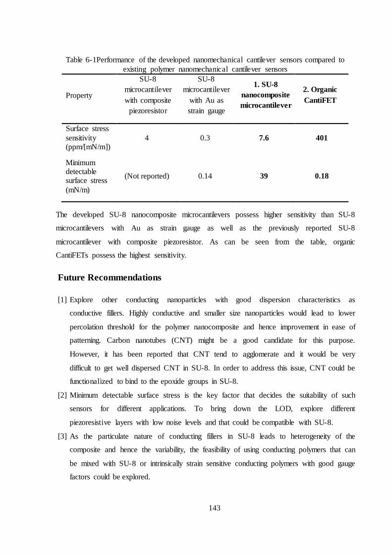
143
Table 6-1Performance of the developed nanomechanical cantilever sensors compared to existing polymer nanomechanical cantilever sensors
Property
SU-8 microcantilever with composite
piezoresistor
SU-8 microcantilever
with Au as strain gauge
1. SU-8 nanocomposite microcantilever
2. Organic CantiFET
Surface stress sensitivity (ppm/[mN/m])
4 0.3 7.6 401
Minimum detectable surface stress (mN/m)
(Not reported) 0.14 39 0.18
The developed SU-8 nanocomposite microcantilevers possess higher sensitivity than SU-8
microcantilevers with Au as strain gauge as well as the previously reported SU-8
microcantilever with composite piezoresistor. As can be seen from the table, organic
CantiFETs possess the highest sensitivity.
Future Recommendations
[1] Explore other conducting nanoparticles with good dispersion characteristics as
conductive fillers. Highly conductive and smaller size nanoparticles would lead to lower
percolation threshold for the polymer nanocomposite and hence improvement in ease of
patterning. Carbon nanotubes (CNT) might be a good candidate for this purpose.
However, it has been reported that CNT tend to agglomerate and it would be very
difficult to get well dispersed CNT in SU-8. In order to address this issue, CNT could be
functionalized to bind to the epoxide groups in SU-8.
[2] Minimum detectable surface stress is the key factor that decides the suitability of such
sensors for different applications. To bring down the LOD, explore different
piezoresistive layers with low noise levels and that could be compatible with SU-8.
[3] As the particulate nature of conducting fillers in SU-8 leads to heterogeneity of the
composite and hence the variability, the feasibility of using conducting polymers that can
be mixed with SU-8 or intrinsically strain sensitive conducting polymers with good gauge
factors could be explored.
144
[4] In the case of detection of explosive vapours, in order to improve upon selectivity aspect,
three approaches could be adopted. (1) Follow microcantilever array approach with
separate coatings that support different types of interactions with the analyte molecules
and then selectively detect the explosives by performing pattern recognition (2)
Functionalize microcantilevers with coating materials very specific (probably
Calixarenes, molecular imprinted polymers) to explosive molecules (3) Use
microcantilevers with other potential explosive sensors such as OFET based explosive
sensors which together could bring orthogonality to the sensing.
[5] In the case of organic CantiFETs, the bias voltage range can still be reduced by using
polymer dielectric with dielectric constant higher than SU-8. Though SU-8 was used as
the dielectric material in the developed organic CantiFETs, better dielectric materials
could be incorporated into the integrated OFET to improve the mobility and to reduce the
bias stress instability.
[6] Polymer materials such as parylene that can be easily deposited at low temperature could
replace the HWCVD silicon nitride encapsulation layer for these CantiFETs.
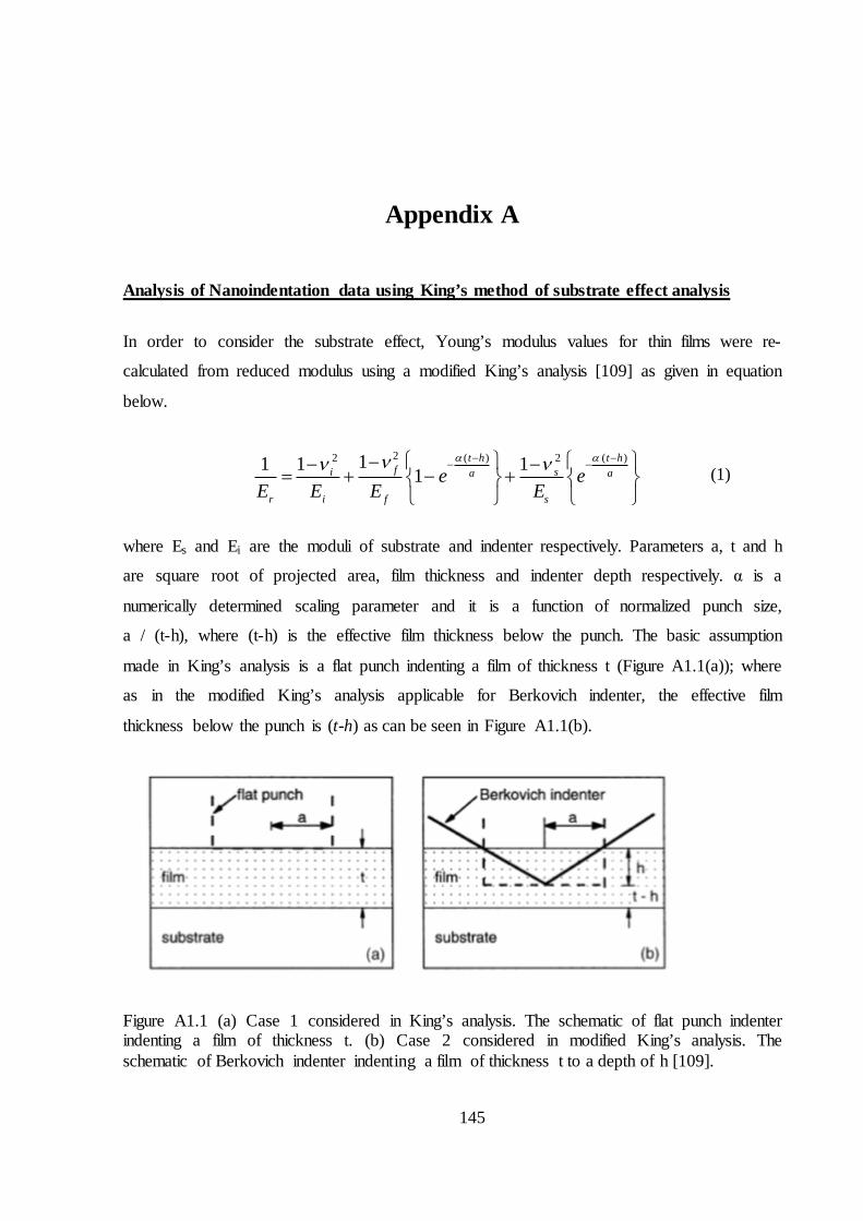
145
Appendix A
Analysis of Nanoindentation data using King’s method of substrate effect analysis
In order to consider the substrate effect, Young’s modulus values for thin films were re-
calculated from reduced modulus using a modified King’s analysis [109] as given in equation
below.
2 ( ) ( )2 211 11 1t h t h
fi sa a
r i f s
e eE E E E
(1)
where Es and Ei are the moduli of substrate and indenter respectively. Parameters a, t and h
are square root of projected area, film thickness and indenter depth respectively. α is a
numerically determined scaling parameter and it is a function of normalized punch size,
a / (t-h), where (t-h) is the effective film thickness below the punch. The basic assumption
made in King’s analysis is a flat punch indenting a film of thickness t (Figure A1.1(a)); where
as in the modified King’s analysis applicable for Berkovich indenter, the effective film
thickness below the punch is (t-h) as can be seen in Figure A1.1(b).
Figure A1.1 (a) Case 1 considered in King’s analysis. The schematic of flat punch indenter indenting a film of thickness t. (b) Case 2 considered in modified King’s analysis. The schematic of Berkovich indenter indenting a film of thickness t to a depth of h [109].
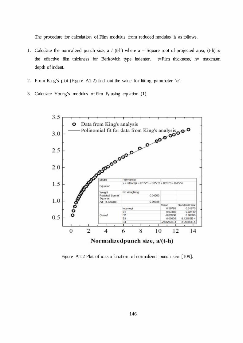
146
The procedure for calculation of Film modulus from reduced modulus is as follows.
1. Calculate the normalized punch size, a / (t-h) where a = Square root of projected area, (t-h) is
the effective film thickness for Berkovich type indenter. t=Film thickness, h= maximum
depth of indent.
2. From King’s plot (Figure A1.2) find out the value for fitting parameter ‘α’.
3. Calculate Young’s modulus of film Ef using equation (1).
Figure A1.2 Plot of α as a function of normalized punch size [109].
147
Appendix B
SU-8/CB nanocomposite for a novel all polymer piezoresistive microaccelerometer4
MEMS accelerometers use a variety of transduction principles, such as capacitive [134],
piezoelectric[135], tunnelling [136] and piezoresistive [137-140] . Among these,
piezoresistive accelerometers seem to be especially attractive due to their structural
simplicity, easier fabrication process and their immunity to parasitic capacitance and
electromagnetic interference. Various research groups have worked on the design, fabrication
and optimization of piezoresistive MEMS accelerometers. However, the reported
piezoresistive micro-accelerometers are silicon based with the associated complex and
expensive fabrication steps such as the SOI wafer processing, double sided alignment, silicon
bulk micromachining, etc. Piezoresistive accelerometers are also considered to be less
sensitive compared to the capacitive accelerometers. However, it has been shown that
sensitivity of the piezoresistive accelerometers can be improved by novel device designs or by
introducing compliant structural materials and high gauge factor piezoresistive elements. The
latter direction very similar to the polymer nanocomposite piezoresistive microcantilevers
presented in this chapter would be an optimum solution for improving the performance and
reducing the cost of production.
SU-8 based piezoresistive MEMS accerometers were developed for the first time by
integrating SU-8/CB nanocomposite strain sensitive layer. The polymer nanocomposite
microaccelerometer has a quad beam structure with a suspended proof mass, surrounded by a
thick frame; all fabricated using SU-8. The outer frame provides support for the beams and a
region for contact pads. Individual beams contain polymer nanocomposite (composite of SU-
8 and Carbon Black) layer sandwiched between two SU-8 layers. The polymer nanocomposite
4 MEMS accelerometer developed in collaboration with Prajakta S Vaidya, M-Tech Batch 2009, Department of Electrical Engineering, IIT Bombay [143].
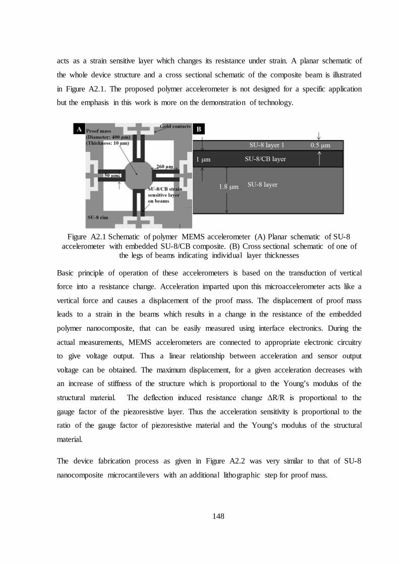
148
acts as a strain sensitive layer which changes its resistance under strain. A planar schematic of
the whole device structure and a cross sectional schematic of the composite beam is illustrated
in Figure A2.1. The proposed polymer accelerometer is not designed for a specific application
but the emphasis in this work is more on the demonstration of technology.
Figure A2.1 Schematic of polymer MEMS accelerometer (A) Planar schematic of SU-8 accelerometer with embedded SU-8/CB composite. (B) Cross sectional schematic of one of
the legs of beams indicating individual layer thicknesses
Basic principle of operation of these accelerometers is based on the transduction of vertical
force into a resistance change. Acceleration imparted upon this microaccelerometer acts like a
vertical force and causes a displacement of the proof mass. The displacement of proof mass
leads to a strain in the beams which results in a change in the resistance of the embedded
polymer nanocomposite, that can be easily measured using interface electronics. During the
actual measurements, MEMS accelerometers are connected to appropriate electronic circuitry
to give voltage output. Thus a linear relationship between acceleration and sensor output
voltage can be obtained. The maximum displacement, for a given acceleration decreases with
an increase of stiffness of the structure which is proportional to the Young’s modulus of the
structural material. The deflection induced resistance change ΔR/R is proportional to the
gauge factor of the piezoresistive layer. Thus the acceleration sensitivity is proportional to the
ratio of the gauge factor of piezoresistive material and the Young’s modulus of the structural
material.
The device fabrication process as given in Figure A2.2 was very similar to that of SU-8
nanocomposite microcantilevers with an additional lithographic step for proof mass.
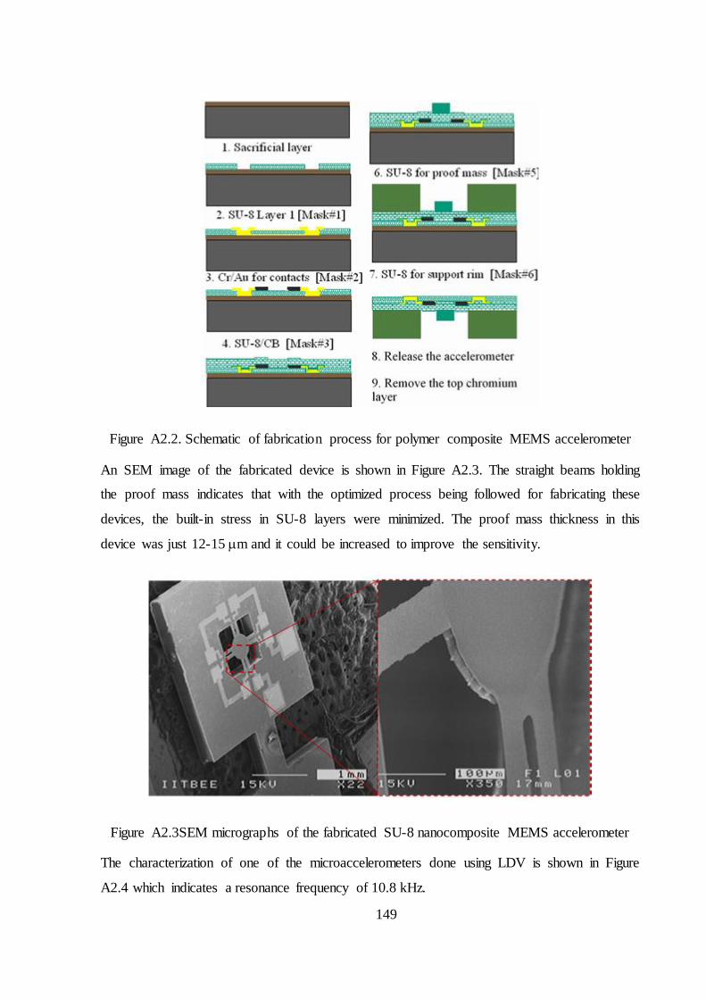
149
Figure A2.2. Schematic of fabrication process for polymer composite MEMS accelerometer
An SEM image of the fabricated device is shown in Figure A2.3. The straight beams holding
the proof mass indicates that with the optimized process being followed for fabricating these
devices, the built-in stress in SU-8 layers were minimized. The proof mass thickness in this
device was just 12-15 m and it could be increased to improve the sensitivity.
Figure A2.3SEM micrographs of the fabricated SU-8 nanocomposite MEMS accelerometer
The characterization of one of the microaccelerometers done using LDV is shown in Figure
A2.4 which indicates a resonance frequency of 10.8 kHz.
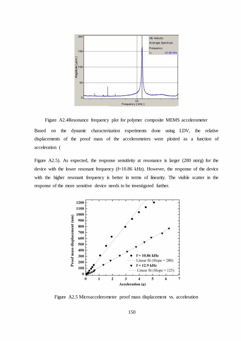
150
Figure A2.4Resonance frequency plot for polymer composite MEMS accelerometer
Based on the dynamic characterization experiments done using LDV, the relative
displacements of the proof mass of the accelerometers were plotted as a function of
acceleration (
Figure A2.5). As expected, the response sensitivity at resonance is larger (280 nm/g) for the
device with the lower resonant frequency (f=10.86 kHz). However, the response of the device
with the higher resonant frequency is better in terms of linearity. The visible scatter in the
response of the more sensitive device needs to be investigated further.
Figure A2.5 Microaccelerometer proof mass displacement vs. acceleration
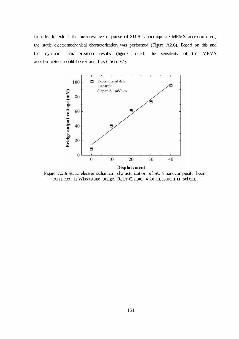
151
In order to extract the piezoresistive response of SU-8 nanocomposite MEMS accelerometers,
the static electromechanical characterization was performed (Figure A2.6). Based on this and
the dynamic characterization results (figure A2.5), the sensitivity of the MEMS
accelerometers could be extracted as 0.56 mV/g.
Figure A2.6 Static electromechanical characterization of SU-8 nanocomposite beam
connected in Wheatstone bridge. Refer Chapter 4 for measurement scheme.

152
Appendix C
I. Common processes
A. Release layers or sacrificial layers for releasing SU-8 microcantilevers
1. RF Sputtered silicon dioxide
Base Vacuum 2 x 10⁻⁶ mbar
Process Vacuum 0.023 mbar
Sputter Gas Argon
Substrate Temperature Room temperature
Thickness (For 55 min) 200 nm
2. Thermally grown silicon dioxide Pyrogenic oxidation @ 1050oC (for 2 hr. 30 min) to yield silicon dioxide thickness
between 800 nm.
B. Physical vapour deposition of metals (Cr, Ti and Au)
1. Thermal evapouration
Method : Resistive thermal evaporation.
Vacuum : 2 x 10⁻⁶ ; Deposition rate for Cr = 0.16 nm/sec at filament current of 81 Amps
Deposition rate for Au = 0.1-0.3 nm/sec for filament current of 70 Amps.
2. RF Sputtering
Parameter Value Cr Ti Au
Base Vacuum 1.3 x 10⁻⁵ mbar
Process Vacuum 1.2 x 10⁻² mbar
Sputter Gas Argon
Substrate Temperature Room temperature
RF Power 150 W 150 W 80 W
Thickness (Dur.: 1min.) 15 nm 3.6 nm 55 nm

153
C. Lift-off patterning of metals (Ti/Au)
1. Take 2-3 ml Positive Resist (PPR) S1813; spin coat @1500 rpm for 35 seconds with a
spread cycle of 500 rpm for 15 seconds
2. Prebake on a hot plate for 12 min at 70oC
3. UV exposure in Karl Suss MJB 3 std. aligner for 1 minute
(@Lamp intensity = 3.4 mW/cm2 )
4. Develop in MF 319 developer for 24 sec.
5. Rinse in water, blow dry. DO NOT HARD BAKE.
6. Deposit Ti/Au film with substrate at room temperature.
Ensure that substrate is not heated for extended periods of time
7. Stir or ultrasonicate in Acetone to lift-off the deposited film from unexposed areas
D. Etching of metals (Cr/Au)
1. Deposit Cr/Au film
2. Take 2 ml Positive Resist (PPR) S1813; spin coat @3000 rpm for 35 seconds with a
spread cycle of 500 rpm for 15 seconds
3. Prebake on a hot plate for 13 min at 70oC
4. UV exposure in Karl Suss MJB 3 std. aligner for 45 sec.
(@Lamp intensity = 3.4 mW/cm2 )
5. Develop in MF 319 developer for 18 sec.
6. Rinse in water, blow dry.
7. Perform etching in respective etchants for Au and Cr. After etching Au, remove PPR
with Acetone. This is very important as the Cr etchant hardens the PPR5. Then perform
the Cr etching. Finally rinse in DI water and blow dry the sample in nitrogen.
5 Private communication with Nidhi Maheswari, Ph.D. student, IIT Bombay
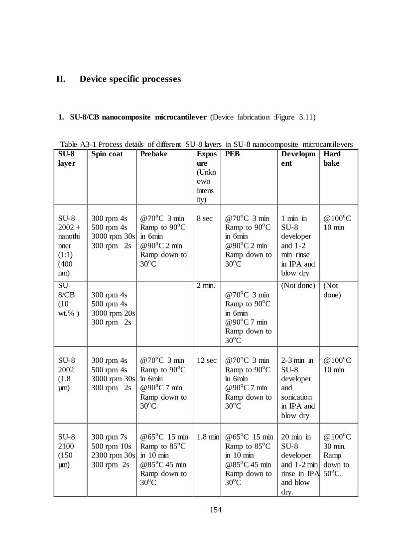
154
II. Device specific processes
1. SU-8/CB nanocomposite microcantilever (Device fabrication :Figure 3.11)
Table A3-1 Process details of different SU-8 layers in SU-8 nanocomposite microcantilevers SU-8 layer
Spin coat
Prebake Exposure (Unknown intensity)
PEB Development
Hard bake
SU-8 2002 + nanothinner (1:1) (400 nm)
300 rpm 4s 500 rpm 4s 3000 rpm 30s 300 rpm 2s
@70oC 3 min Ramp to 90oC in 6min @90oC 2 min Ramp down to 30oC
8 sec
@70oC 3 min Ramp to 90oC in 6min @90oC 2 min Ramp down to 30oC
1 min in SU-8 developer and 1-2 min rinse in IPA and blow dry
@100oC 10 min
SU-8/CB (10 wt.% )
300 rpm 4s 500 rpm 4s 3000 rpm 20s 300 rpm 2s
2 min. @70oC 3 min Ramp to 90oC in 6min @90oC 7 min Ramp down to 30oC
(Not done) (Not done)
SU-8 2002 (1.8 µm)
300 rpm 4s 500 rpm 4s 3000 rpm 30s 300 rpm 2s
@70oC 3 min Ramp to 90oC in 6min @90oC 7 min Ramp down to 30oC
12 sec
@70oC 3 min Ramp to 90oC in 6min @90oC 7 min Ramp down to 30oC
2-3 min in SU-8 developer and sonication in IPA and blow dry
@100oC 10 min
SU-8 2100 (150 µm)
300 rpm 7s 500 rpm 10s 2300 rpm 30s 300 rpm 2s
@65oC 15 min Ramp to 85oC in 10 min @85oC 45 min Ramp down to 30oC
1.8 min
@65oC 15 min Ramp to 85oC in 10 min @85oC 45 min Ramp down to 30oC
20 min in SU-8 developer and 1-2 min rinse in IPA and blow dry.
@100oC 30 min. Ramp down to 50oC.
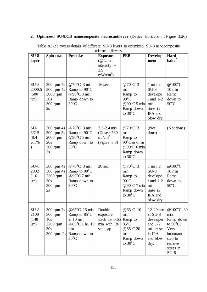
155
2. Optimized SU-8/CB nanocomposite microcantilever (Device fabrication : Figure 3.26)
Table A3-2 Process details of different SU-8 layers in optimized SU-8 nanocomposite microcantilevers
SU-8 layer
Spin coat
Prebake Exposure (@Lamp intensity = 3.9 mW/cm2)
PEB Development
Hard bake*
SU-8 2000.5 (500 nm)
300 rpm 4s 500 rpm 4s 3000 rpm 30s 300 rpm 2s
@70oC 3 min Ramp to 90oC @90oC 3 min Ramp down to 30oC
16 sec
@70oC 3 min Ramp to 90oC @90oC 5 min Ramp down to 30oC
1 min in SU-8 developer and 1-2 min rinse in IPA and blow dry
@100oC 10 min Ramp down to 50oC
SU-8/CB (8.4 vol.% )
300 rpm 4s 500 rpm 5s 2000 rpm 20s 300 rpm 2s
@70oC 3 min Ramp to 90oC @90oC 5 min Ramp down to 30oC
2.3-2.4 min (Dose : 530 mJ/cm2 (Figure 3.3)
@70oC 3 min Ramp to 90oC in 6min @90oC 6 min Ramp down to 30oC
(Not done)
(Not done)
SU-8 2002 (1.6 µm)
300 rpm 4s 500 rpm 4s 2300 rpm 30s 300 rpm 2s
@70oC 3 min Ramp to 90oC @90oC 7 min Ramp down to 30oC
20 sec
@70oC 3 min Ramp to 90oC @90oC 7 min Ramp down to 30oC
1 min in SU-8 developer and 1-2 min rinse in IPA and blow dry
@100oC 10 min Ramp down to 50oC
SU-8 2100 (148 µm)
300 rpm 7s 500 rpm 10s 2200 rpm 30s 300 rpm 2s
@65oC 15 min Ramp to 85oC in 10 min @85oC 1 hr. 10 min Ramp down to 30oC
Double exposure. Each for 0.65 min with 30 sec. gap
@65oC 10 min Ramp to 85oC @85oC 20 min Ramp down to 30oC
12-20 min in SU-8 developer and 1-2 min rinse in IPA and blow dry.
@100oC 30 min. Ramp down to 50oC. Very important step to remove stress in SU-8
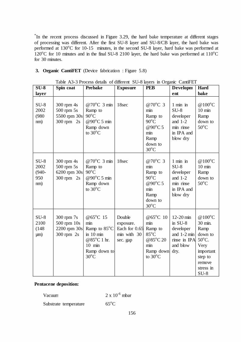
156
*In the recent process discussed in Figure 3.29, the hard bake temperature at different stages of processing was different. After the first SU-8 layer and SU-8/CB layer, the hard bake was performed at 130oC for 10-15 minutes, in the second SU-8 layer, hard bake was performed at 120oC for 10 minutes and in the final SU-8 2100 layer, the hard bake was performed at 110oC for 30 minutes.
3. Organic CantiFET (Device fabrication : Figure 5.8)
Table A3-3 Process details of different SU-8 layers in Organic CantiFET SU-8 layer
Spin coat
Prebake Exposure PEB Development
Hard bake
SU-8 2002 (980 nm)
300 rpm 4s 500 rpm 5s 5500 rpm 30s 300 rpm 2s
@70oC 3 min Ramp to 90oC @90oC 5 min Ramp down to 30oC
18sec
@70oC 3 min Ramp to 90oC @90oC 5 min Ramp down to 30oC
1 min in SU-8 developer and 1-2 min rinse in IPA and blow dry
@100oC 10 min Ramp down to 50oC
SU-8 2002 (940-950 nm)
300 rpm 4s 500 rpm 5s 6200 rpm 30s 300 rpm 2s
@70oC 3 min Ramp to 90oC @90oC 5 min Ramp down to 30oC
18sec
@70oC 3 min Ramp to 90oC @90oC 5 min Ramp down to 30oC
1 min in SU-8 developer and 1-2 min rinse in IPA and blow dry
@100oC 10 min Ramp down to 50oC
SU-8 2100 (148 µm)
300 rpm 7s 500 rpm 10s 2200 rpm 30s 300 rpm 2s
@65oC 15 min Ramp to 85oC in 10 min @85oC 1 hr. 10 min Ramp down to 30oC
Double exposure. Each for 0.65 min with 30 sec. gap
@65oC 10 min Ramp to 85oC @85oC 20 min Ramp down to 30oC
12-20 min in SU-8 developer and 1-2 min rinse in IPA and blow dry.
@100oC 30 min. Ramp down to 50oC. Very important step to remove stress in SU-8
Pentacene deposition:
Vacuum 2 x 10⁻⁶ mbar
Substrate temperature 65oC
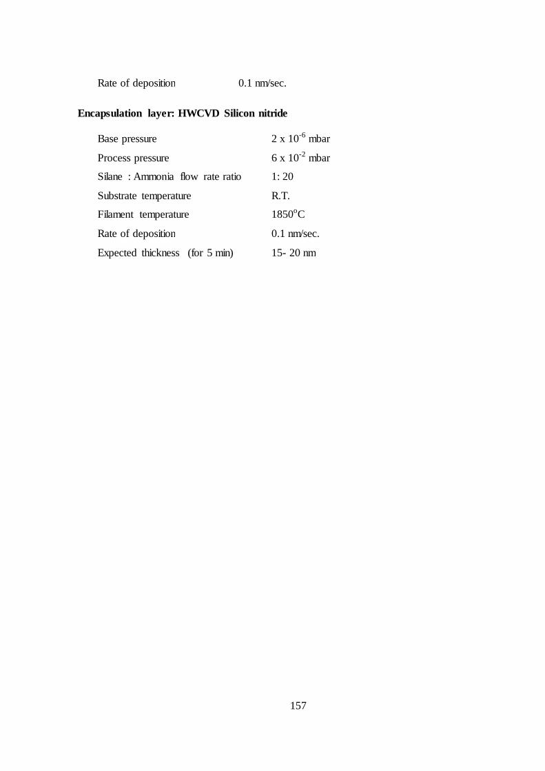
157
Rate of deposition 0.1 nm/sec.
Encapsulation layer: HWCVD Silicon nitride
Base pressure 2 x 10⁻⁶ mbar
Process pressure 6 x 10⁻² mbar
Silane : Ammonia flow rate ratio 1: 20
Substrate temperature R.T.
Filament temperature 1850oC
Rate of deposition 0.1 nm/sec.
Expected thickness (for 5 min) 15- 20 nm
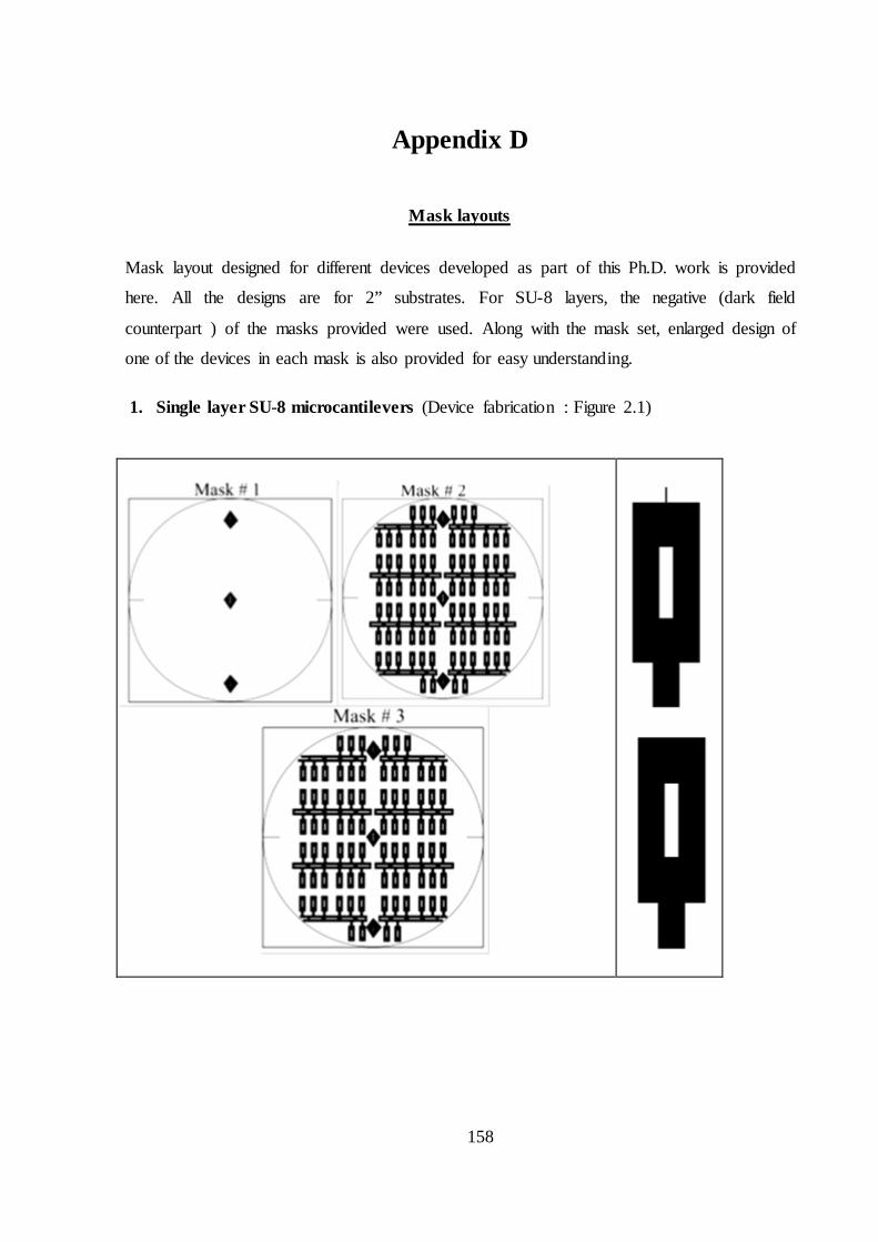
158
Appendix D
Mask layouts
Mask layout designed for different devices developed as part of this Ph.D. work is provided
here. All the designs are for 2” substrates. For SU-8 layers, the negative (dark field
counterpart ) of the masks provided were used. Along with the mask set, enlarged design of
one of the devices in each mask is also provided for easy understanding.
1. Single layer SU-8 microcantilevers (Device fabrication : Figure 2.1)
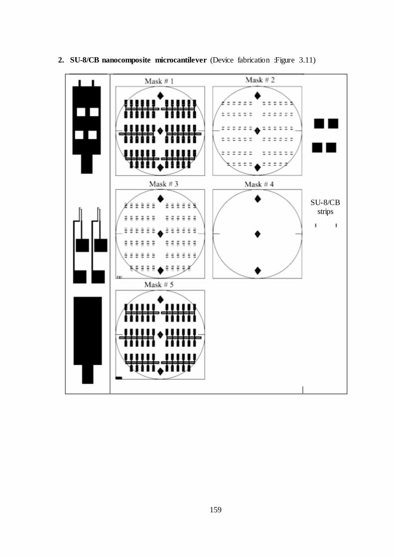
159
2. SU-8/CB nanocomposite microcantilever (Device fabrication :Figure 3.11)
SU-8/CB strips
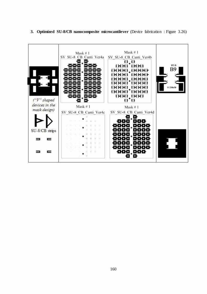
160
3. Optimized SU-8/CB nanocomposite microcantilever (Device fabrication : Figure 3.26)
(“V” shaped devices in the mask design)
SU-8/CB strips
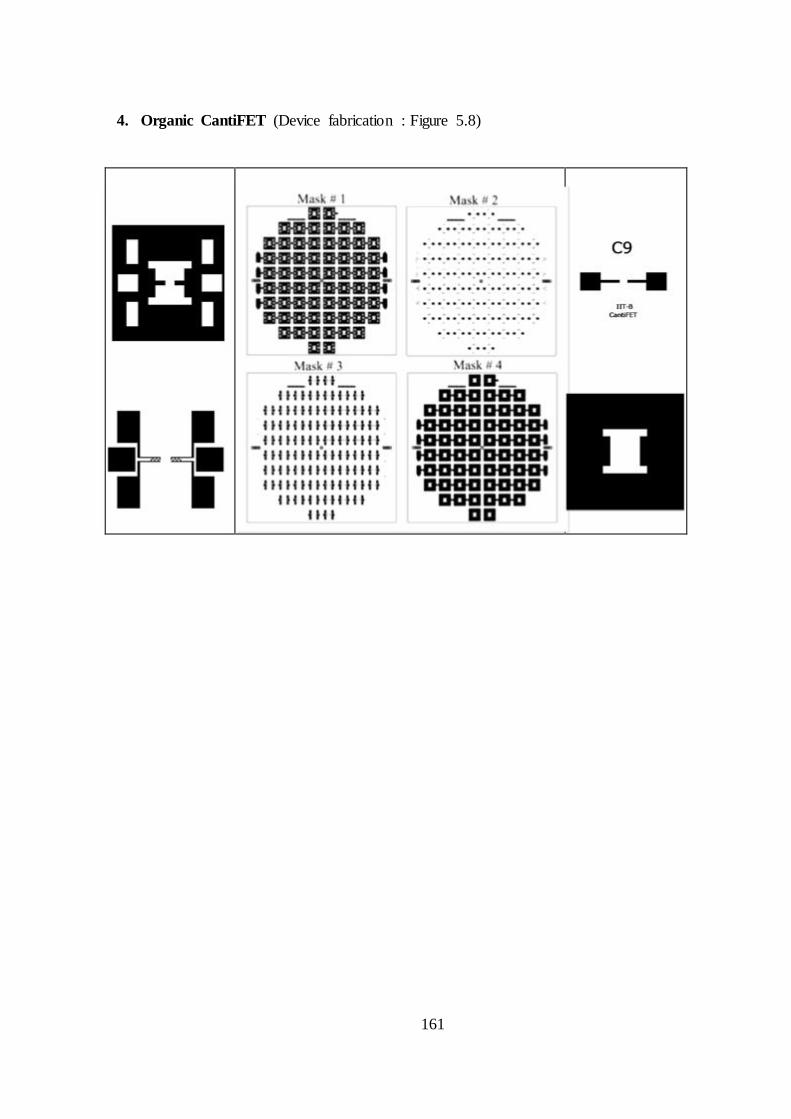
161
4. Organic CantiFET (Device fabrication : Figure 5.8)

162
Appendix E
Spring constant and resonant frequency
Resonant frequency of a cantilever beam in first mode of vibration could be written as
*1
2eff
resk
fm
Here, effk : Effective spring constant, m* : effective mass of the beam.
Case 1: Single layer cantilever beam
33
effEIkL
Here, I: Area moment of inertia; E: Young’s modulus of the cantilever structural material; L: Length of the cantilever beam
For a rectangular cantilever beam, 3
12WhI ;
* 0.243m L W h
Here, W: Width of the rectangular cantilever beam; h: Thickness of the beam; : Density
For a “U” shaped cantilever beam, 3
6WhI ;
* 2 0.243m L W h
Here, W: Width of the rectangular cantilever beam; h: Thickness of the beam; : Density
For a “V” shaped cantilever beam[141] 3
31 1 46
WI bhb
;
* 0.163m L b h

163
Case 2: Multi layer cantilever beam
Consider the case of a multilayer composite beam.
The effective spring constant, 3(3 )eff
effEI
kL
Here, eff i ii
EI E I is for the composite structure.
Ei : Young’s modulus of the ith layer; Ii : Area moment of inertia of the ith layer.
For a rectangular beam, 3
2
12i
i i i NWhI Wh h h
Here hi : Thickness of the ith layer ; hN : Position of the neutral axis.
164
References
[1] J. w Gardner and V.K. Varadan, Osama O. Awadelkarim, Microsensors, MEMS and Smart devices, John Wiley & Sons, 2002.
[2] Bharat Bhushan, “Introduction to Nanotechnology,” Springer Handbook of Nanotechnology, B. Bhushan, ed., Springer, , pp. 1-10.
[3] S.P. Mohanty and E. Kougianos, “Biosensors : A Tutorial Review,” IEEE Potentials, 2006, pp. 1-16.
[4] King W P et.al., “Design of atomic force microscope cantilevers for combined thermomechanical writing and thermal reading in array operation,” J. Microelectromech. Syst., vol. 11, p. 765–74.
[5] B. R, L.H. P, G. Ch, G.J. K, F.J. H, S. L, and M.E. and G¨. H-J, “Micromechanical thermogravimetry,” Chem. Phys. Lett., vol. 294, p. 363–9.
[6] S.-hyung S. Lim, D. Raorane, S. Satyanarayana, and A. Majumdar, “Nano-chemo-mechanical sensor array platform for high-throughput chemical analysis,” Sensors And Actuators, vol. 119, 2006, pp. 466-474.
[7] Y. Arntz, J.D. Seelig, H.P. Lang, J. Zhang, P. Hunziker, J.P. Ramseyer, E. Meyer, M. Hegner, and C. Gerber, “Label-free protein assay based on a nanomechanical cantilever array,” vol. 14, 2003, pp. 86-90.
[8] L.G. Carrascosa and M. Moreno, “Nanomechanical biosensors : a new sensing tool,” Trends Anal. Chem., vol. 25, 2005, p. 196–206.
[9] C. Ziegler, “Cantilever-based biosensors,” Analytical and Bioanalytical Chemistry, vol. 379, 2004, pp. 946-959.
[10] J. Fritz, M.K. Baller, H.P. Lang, and H. Rothuizen, “Translating Biomolecular Recognition into Nanomechanics,” Science, vol. 288, 2000, pp. 316-318.
[11] J.W. Gardner, JehudaYinon, ed., Electronic Noses & Sensors for the Detection of Explosives, NATO Science series, .
[12] H.-peter Lang, M. Hegner, and C. Gerber, “Nanomechanical Cantilever Array Sensors,” Handbook of Nanotechnology, Springer, , pp. 443-459.
[13] Stoney G G, “The tension of metallic films deposited by electrolysis,” Proc. R. Soc. Lond. A, vol. 82, 1909, p. 172.
[14] R. Raiteri, “Micromechanical cantilever-based biosensors,” Sensors and Actuators B: Chemical, 2001.
165
[15] N.V. Lavrik and M.J. Sepaniak, “Cantilever transducers as a platform for chemical and biological sensors,” Review of Scientific Instruments, vol. 75, 2004, pp. 29-33.
[16] R. Berger, E. Delamarche, H.P. Lang, C. Gerber, J.K. Gimzewski, E. Meyer, and H. Güntherodt, “Surface stress in the self-assembly of alkanethiols on gold probed by a force microscopy technique,” Applied Physics A: Mater.Sci.Process, vol. 66, 1998, pp. 55-59.
[17] R. Berger, E. Delamarche, H.P. Lang, C. Gerber, J.K. Gimzewski, E. Meyer, and H.-joachim Gu, “Surface Stress in the Self-Assembly of Alkanethiols on Gold Ru,” Science, vol. 276, 1997, pp. 2021-2024.
[18] K.W. Wee, “Novel electrical detection of label-free disease marker proteins using piezoresistive self-sensing micro-cantilevers,” Biosensors and Bioelectronics,, 2005.
[19] G. Wu, H. Ji, K. Hansen, T. Thundat, R. Datar, R. Cote, M.F. Hagan, A.K. Chakraborty, and A. Majumdar, “Origin of nanomechanical cantilever motion generated from biomolecular interactions,” Materials Science, 2001, pp. 18-22.
[20] K.M. Hansen and T. Thundat, “Microcantilever biosensors,” Methods, vol. 37, 2008, pp. 57-64.
[21] L.A. Pinnaduwage, D.L. Hedden, A. Gehl, V.I. Boiadjiev, J.E. Hawk, R.H. Farahi, and T. Thundat, “A sensitive , handheld vapor sensor based on microcantilevers,” Review of Scientific Instruments, vol. 75, 2008, pp. 4554-4557.
[22] A.R. Krause, C.V. Neste, L. Senesac, T. Thundat, and E. Finot, “Trace explosive detection using photothermal deflection spectroscopy,” Journal of Applied Physics, vol. 103, 2008, p. 094906.
[23] C.W.V. Neste, L.R. Senesac, D. Yi, and T. Thundat, “Standoff detection of explosive residues using photothermal microcantilevers,” 2008, pp. 2008-2010.
[24] L. Senesac and T.G. Thundat, “Nanosensors for trace explosive detection,” Materialstoday, vol. 11, 2008, pp. 28-36.
[25] L.A. Pinnaduwage, A. Wig, D.L. Hedden, A. Gehl, D. Yi, T. Thundat, R.T. Lareau, and I. Introduction, “Detection of trinitrotoluene via deflagration on a microcantilever,” Journal of Applied Physics, vol. 95, 2004, pp. 5871-5875.
[26] K.M. Hansen and T. Thundat, “Microcantilever biosensors,” Methods, vol. 37, 2008, pp. 57-64.
[27] M.A. and B.A. Greve A, Keller S, Vig A L, Kristensen A, Larsson D, Yvind K, Hvam J M, Cerruti M, “Thermoplastic microcantilevers fabricated by nanoimprint lithography,” J. Micromech. Microeng., vol. 20, 2010, p. 015009.
166
[28] L.Y. and X.Y. Katragadda R, Wang Z, Khalid W, “Parylene cantilevers integrated with polycrystalline silicon piezoresistors for surface stress sensing,” Appl. Phys. Lett., vol. 91, 2007, p. 083505.
[29] A. Boisen, S. Dohn, S.S. Keller, S. Schmid, and M. Tenje, “Cantilever- like micromechanical sensors,” Rep. Prog. Phys., vol. 74, 2011, pp. 1-30.
[30] J.M. Shaw, J.D. Gelorme, N.C. LaBianca, W.E. Conley, and S.J. Holmes, “Negative photoresists for optical lithography,” IBM Journal of Research and Development, vol. 41, 1997, pp. 81-94.
[31] J. Brugger, P. Renaud, and P. Vettiger, with M. Despont and H. Lorenz, N.Fahrni, “High aspect ratio ultrathick, negative-tone near-UV photoresist for MEMS applications,” IEEE MEMS, 1997, pp. 518-522.
[32] H. Lorenz, M. Despont, M. Fahrni, N. LaBianca, P. Vettiger, and P. Renaud, “SU-8: a low-cost negative resist for MEMS,” J. Micromech. Microeng, vol. 7, 1997, pp. 121-124.
[33] de R.N.F. and A.D. Genolet G, Brugger J, Despont M, Drechsler U, Vettiger P, “Soft, entirely photoplastic probes for scanning force microscopy,” Rev. Sci. Instrum., vol. 70, 1999, p. 2398.
[34] J. Theysen, A.D. Yalcinkaya, P. Vettiger, and A. Menon, “Polymer-based stress sensor with integrated readout,” Journal of Physics D: Applied Physics, vol. 35, 2002, pp. 2698-2703.
[35] J.H.T. Ransley, M. Watari, D. Sukumaran, and R.A. McKendry, A.A. Seshia, “SU8 bio-chemical sensor microarrays,” Microelectronic Engineering, vol. 83, 2006, pp. 1621-1625.
[36] M. Nordström, S. Keller, M. Lillemose, A. Johansson, S. Dohn, D. Haefliger, G. Blagoi, M. Havsteen-jakobsen, and A. Boisen, “SU-8 Cantilevers for Bio/chemical Sensing; Fabrication, Characterisation and Development of Novel Read-out Methods,” Sensors, 2008, pp. 1595-1612.
[37] H P Lang et.al, “Sequential position readout from arrays of micromechanical cantilever sensors,” Appl. Phys. Lett., vol. 72, 1998, p. 383.
[38] H P Lang, “A chemical sensor based on a micromechanical cantilever array for the identification of gases and vapors,” Appl. Phys. A, vol. 66, 1998.
[39] C.A. Savran, T.P. Burg, J. Fritz, and S.R. Manalis, “Microfabricated mechanical biosensor with inherently differential readout,” Applied Physics Letters, vol. 83, 2003, pp. 1659-1661.
[40] S.-hyung S. Lim, D. Raorane, S. Satyanarayana, and A. Majumdar, “Nano-chemo-mechanical sensor array platform for high-throughput chemical analysis,” Sensors And Actuators, vol. 119, 2006, pp. 466-474.
167
[41] M. Yue, H. Lin, D.E. Dedrick, S. Satyanarayana, A. Majumdar, A.S. Bedekar, J.W. Jenkins, and S. Sundaram, “A 2-D Microcantilever Array for Multiplexed Biomolecular Analysis,” Journal Of Microelectromechanical Systems, vol. 13, 2004, pp. 290-299.
[42] B.A.A. Barlian, W.-tae Park, J.R. Mallon, A.J. Rastegar, and B.L. Pruitt, “Review : Semiconductor Piezoresistance for Microsystems,” Proceedings of the IEEE, vol. 97, 2009.
[43] A.A. Barlian, W.-tae Park, J.R.M. Jr, A.J. Rastegar, B.L. Pruitt, and M. Engineering, “Review: Semiconductor Piezoresistance for Microsystems,” Proc IEEE Inst Electr Electron Eng, vol. 97, 2009, pp. 513-552.
[44] J.H. and H.O. Boisen A, Thaysen J, “Environmental sensors based on micromachined cantilevers with integrated read-out,” Ultramicroscopy, vol. 82, 2000, p. 11.
[45] S.T. and G.C. Yoshikawa G, Lang H P, Akiyama T, Aeschimann L, Staufer U, Vettiger P, Aono M, “Sub-ppm detection of vapors using piezoresistive microcantilever array sensors,” Nanotechnology, vol. 20, 2009, p. 15501.
[46] F.T. Goericke and W.P. King, “Modeling Piezoresistive Microcantilever Sensor Response to Surface Stress for Biochemical Sensors,” IEEE Sensors, vol. 8, 2008, pp. 1404-1410.
[47] P.S. J, D.J. C, and B.L. Pruitt, “Piezoresistive cantilever performance: I. Analytical model for sensitivity.,” J. Microelectromech. Syst, vol. 19, 2010, p. 137.
[48] S.-J. Park, J.C. Doll, A.J. Rastegar, and B.L. Pruitt, “Piezoresistive Cantilever Performance—Part II: Optimization,” J Microelectromech Syst., vol. 19, 2010, pp. 149-161.
[49] B. N, B. J, de R.N. F, and D. U, “Scanning force microscopy in the dynamic mode using microfabricated capacitive sensors,” J. Vac. Sci. Technol. B, vol. 14, 1996, p. 901.
[50] G. Shekhawat, S.-H. Tark, and V.P. Dravid, “MOSFET-Embedded Microcantilevers for Measuring Deflection in Biomolecular Sensors,” Science, vol. 311, 2006, pp. 1592-1595.
[51] J. Thaysen, A.D. Yalçinkaya, R.K. Vestergaard, S. Jensen, M.W. Mortensen, P. Vettiger, and A. Menon, “SU-8 BASED PIEZORESISTIVE MECHANICAL SENSOR,” IEEE MEMS, 2002, pp. 320-323.
[52] N.S. Kale, S. Nag, R. Pinto, V.R. Rao, and S. Member, “Fabrication and Characterization of a Polymeric Microcantilever With an Encapsulated Hotwire CVD Polysilicon Piezoresistor,” Journal Of Microelectromechanical Systems, 2008, pp. 1-9.
[53] N.S. Kale, “Making Hotwire CVD a Viable Technology Alternative for BioMEMS Applications : Device Optimization , Fabrication and Characterization,” 2007.
168
[54] X.-wu Zhang, Y.I. Pan, Q. Zheng, and X.-su Yi, “Time Dependence of Piezoresistance for the Conductor-,” Polymer, 2000, pp. 2739-2749.
[55] M.H.G. Wichmann, S.T. Buschhorn, J. Gehrmann, and K. Schulte, “Piezoresistive response of epoxy composites with carbon nanoparticles under tensile load,” vol. c, 2009, pp. 1-8.
[56] H.C. Chiamori, J.W. Brown, E.V. Adhiprakasha, and E.T. Hantsoo, “Suspension of nanoparticles in SU-8 : Processing and characterization of nanocomposite polymers,” Microelectronics Journal, vol. 39, 2008, pp. 228-236.
[57] L. Gammelgaard, P.A. Rasmussen, M. Calleja, P. Vettiger, and A. Boisen, “Microfabricated photoplastic cantilever with integrated photoplastic/carbon based piezoresistive strain sensor,” Applied Physics Letters, vol. 88, 2006, p. 113508.
[58] R. Mateiu, M. Lillemose, T. Steen, A. Boisen, and O. Geschke, “Reliability of poly 3 , 4-ethylenedioxythiophene strain gauge,” Microelectronic Engineering, vol. 84, 2007, pp. 1270-1273.
[59] M. Lillemose, M. Spieser, N.O. Christiansen, A. Christensen, and A. Boisen, “Intrinsically conductive polymer thin film piezoresistors,” Microelectronic Engineering, vol. 85, 2008, pp. 969-971.
[60] T. Ji, S. Jung, and V.K. Varadan, “Field-Controllable Flexible Strain Sensors Using Pentacene Semiconductors,” IEEE Electron Device Letters, vol. 28, 2007, pp. 1105-1107.
[61] T. Sekitani, Y. Kato, S. Iba, H. Shinaoka, and T. Someya, “Bending experiment on pentacene field-effect transistors on plastic films,” Applied Physics Letters, 2005, pp. 3-5.
[62] T. Sekitani, U. Zschieschang, H. Klauk, and T. Someya, “Flexible organic transistors and circuits with extreme bending stability,” Nature Materials, vol. 9, 2010, p. 1015.
[63] A. Jedaa and M. Halik, “Toward strain resistant flexible organic thin film transistors,” Applied Physics Letters, vol. 95, 2009, p. 103309.
[64] T. Sekitani, S. Iba, Y. Kato, Y. Noguchi, and T. Someya, “Ultraflexible organic field-effect transistors embedded at a neutral strain position,” Applied Physics Letters, vol. 87, 2005, p. 173502.
[65] C. Yang, J. Yoon, S.H. Kim, K. Hong, D.S. Chung, K. Heo, C.E. Park, and M. Ree, “Bending-stress-driven phase transitions in pentacene thin films for flexible organic field-effect transistors,” Applied Physics Letters, vol. 92, 2008, p. 243305.
[66] M. Kanari, M. Kunimoto, T. Wakamatsu, and I. Ihara, “Critical bending radius and electrical behaviors of organic field effect transistors under elastoplastic bending strain,” Thin Solid Films, vol. 518, 2010, pp. 2764-2768.
169
[67] G. Darlinski, U. Böttger, R. Waser, H. Klauk, M. Halik, U. Zschieschang, G. Schmid, and C. Dehm, “Mechanical force sensors using organic thin-film transistors,” Journal of Applied Physics, vol. 97, 2005, p. 093708.
[68] I. Manunza, A. Sulis, and A. Bonfiglio, “Pressure sensing by flexible, organic, field effect transistors,” Applied Physics Letters, vol. 89, 2006, p. 143502.
[69] I. Manunza and A. Bonfiglio, “Pressure sensing using a completely flexible organic transistor,” Biosensors and Bioelectronics, vol. 22, 2007, pp. 2775-2779.
[70] M. Kitamura and Y. Arakawa, “Pentacene-based organic field-effect,” J. Phys.: Condens. Matter, vol. 20, 2008, p. 184011.
[71] S. Jung, T. Ji, and V.K. Varadan, “Pentacene-Based Low-Voltage Strain Sensors With PVP/Ta2O5 Hybrid Gate Dielectrics,” IEEE Transactions on Electron Devices, vol. 57, 2010, pp. 391-396.
[72] T. Thundat, E. A. Wachter and S.L. SharpR. J. Warmack, “""” Appl. Phys. Lett., vol. 66, 1995, p. 1695.
[73] P.G. Datskos, I. Sauers, “""” Sens. Actuators B, vol. 61, 1999, p. 75.
[74] C. L. Britton et.al, “C. L. Britton et. al,” Ultramicroscopy, vol. 82, 2000, p. 17.
[75] T. Thundat, G.Y. Chen, R.J. Warmack, and D.P. Allison, E. A. Wachter, “""” Anal. Chem., vol. 67, 1995, p. 519.
[76] R. Berger, C. Gerber, and H.P. Lang, J. K. Gimzewski, “""” Microelectron. Eng., vol. 35, 1997, p. 373.
[77] S.K. Vashist, “A Review of Microcantilevers for Sensing Applications,” Journal of Nanotechnology Online, 2007, p. http://www.azonano.com/Details.asp?ArticleID=1927.
[78] A. Subramanian, P.I. Oden, S.J. Kennel, K.B. Jacobson, R.J. Warmack, T. Thundat, and M.J. Doktycz, “""” Appl. Phys. Lett., vol. 81, 2002, p. 385.
[79] N.V. Lavrik and M.J. Sepaniak, “Cantilever transducers as a platform for chemical and biological sensors,” Review of Scientific Instruments, vol. 75, 2004, pp. 29-33.
[80] D. Yi, A. Greve, J.H. Hales, L.R. Senesac, Z.J. Davis, D.M. Nicholson, A. Boisen, and T. Thundat, “Detection of adsorbed explosive molecules using thermal response of suspended microfabricated bridges,” Applied Physics Letters, vol. 93, 2008, p. 154102.
[81] L.R. Senesac, D. Yi, A. Greve, J.H. Hales, Z.J. Davis, D.M. Nicholson, A. Boisen, and T. Thundat, “Micro-differential thermal analysis detection of adsorbed explosive molecules using microfabricated bridges,” Review of Scientific Instruments, vol. 80, 2009, p. 035102.
170
[82] P.L. Edmiston, D.P. Campbell, D.S. Gottfried, J. Baughman, and M.M. Timmers, “Sensors and Actuators B : Chemical Detection of vapor phase trinitrotoluene in the parts-per-trillion range using waveguide interferometry,” Response, vol. 143, 2010, pp. 574-582.
[83] L.A. Pinnaduwage, A.C. Gehl, and S.L. Allman, “Miniature sensor suitable for electronic nose applications,” Review of Scientific Instruments, vol. 78, 2007, p. 055101.
[84] 2010L.X., with C. Y, Xu P, “Self-assembling siloxane bilayer directly on SiO2 surface of micro-cantilevers for long-term highly repeatable sensing to trace explosives,” Nanotechnology, vol. 21, 2010, p. 26550.
[85] Y. Chen, P.C. Xu, Y. Liu, T.T. Yang, Y.L. Yang, and X.X. Li, “A NOVEL METHOD OF SELF-ASSEMBLING SILOXANE BI-LAYER DIRECTLY ON S I O 2 SURFACE OF MICRO-CANTILEVER FOR LONG-TERM REPEATABLE SENSING TO TRACE EXPLOSIVES State Key Lab of Transducer Technology , Shanghai Institute of Microsystem and Information Technology,” Transducers, 2009, pp. 600-603.
[86] P. Xu, H. Yu, X. Gan, M. Liu, X. Li, and C. Academy, “RESONANT CANTILEVERS WITH ULTRA-DENSELY INWALL- FUNCTIONALIZED MESOPOROUS-SILICA SENSING-LAYER FOR DETECTION OF ppt-LEVEL TNT State Key Lab of Transducer technology , Shanghai Institute of Microsystem and Information ( a ) ( b ) ( c ) ( d ),” 23rd International Conference on MicroElectroMechanical Systems (IEEE MEMS), 2010, pp. 128-131.
[87] “www.microchem.com.”
[88] “http://www.geocities.ws/guerinlj/.”
[89] “http://memscyclopedia.org/su8.html.”
[90] Grégoire GENOLET, “NEW PHOTOPLASTIC FABRICATION TECHNIQUES AND DEVICES BASED ON HIGH ASPECT RATIO PHOTORESIST,” 2001.
[91] S.D. Psoma and D.W.K. Jenkins, “COMPARATIVE ASSESSMENT OF DIFFERENT SACRIFICIAL MATERIALS FOR RELEASING SU-8 STRUCTURES,” Rev.Adv.Mat.Sci, vol. 10, 2005, pp. 149-155.
[92] P.A. Rasmussen and A. Boisen, “Dry release of all-polymer structures,” Microelectronic Engineering, vol. 79, 2005, pp. 88-92.
[93] S. Mouaziz, G. Boero, and R.S. Popovic, “Polymer-Based Cantilevers With Integrated Electrodes,” Journal Of Microelectromechanical Systems, vol. 15, 2006, pp. 890-895.
[94] S.J.H. I, S. Choi, Y. Choi, M. Alien, and G.S. May, “Characterization of low-temperature SU-8 photoresist processing for MEMS applications,” ASMCʼ04, 2004, pp. 404-408.
171
[95] D. Sameoto, S.-h Tsang, I.G. Foulds, S.-w Lee, and M. Parameswaran, “Control of the out-of-plane curvature in SU-8 compliant microstructures by exposure dose and baking times,” Journal of Micromechanics and Microengineering, vol. 17, 2007, pp. 1093-1098.
[96] R. Feng and R.J. Farris, “Influence of processing conditions on the thermal andmechanical properties of SU8 negative photoresist coatings,” J.Micromech.Microeng., vol. 13, 2003, pp. 80-88.
[97] D. Raorane, S.-hyung S. Lim, and A. Majumdar, “Nanomechanical Assay to Investigate the Selectivity of Binding Interactions,” Nano Letters, 2008, pp. 1-7.
[98] V. Panwar, V.K. Sachdev, and R.M. Mehra, “POLYMER Insulator conductor transition in low-density polyethylene – graphite composites,” European Polymer Journal, vol. 43, 2007, pp. 573-585.
[99] E. Station, “Percolation phenomena in polymer / carbon composites,” Journal of material science letters, vol. 7, 1988, pp. 459-462.
[100] T. Blythe and D. Bloor, Electrical Properties of Polymers, Cambridge: Cambridge University Press, .
[101] G.R. Ruschau, S. Yoshikawa, and R.E. Newnham, “Resistivities of conductive composites,” J. Appl. Phys., vol. 72, 1992, pp. 953-959.
[102] H.P. Xu, Y.H. Wu, D.D. Yang, J.R. Wang, and H.Q. Xie, “STUDY ON THEORIES AND INFLUENCE FACTORS OF PTC PROPERTY IN POLYMER-BASED CONDUCTIVE COMPOSITES,” Rev.Adv.Mat.Sci, vol. 27, 2011, pp. 173-183.
[103] J. Thaysen, “Cantilever for biochemical sensing integrated in a microliquid handling system,” 2001.
[104] “http://www.bic.com/literature/lit_theory_01.html.”
[105] “http://www.bic.com/products/particle_sizing/p_PS_BI-200SM.html.”
[106] W.D. Nix, “Elastic and plastic properties of thin films on substrates : nanoindentation techniques,” Materials Science and engineering, vol. A234-236, 1997, pp. 37-44.
[107] W.C. Oliver and G.M. Pharr, “Measurement of hardness and elastic modulus by instrumented indentation: Advances in understanding and refinements to methodology,” J. Mat. Res., vol. 19, 2004, pp. 3-20.
[108] D. Tranchida, S. Piccarolo, J. Loos, A. Alexeev, D. Tranchida, S. Piccarolo, J. Loos, and A. Alexeev, “Mechanical Characterization of Polymers on a Nanometer Scale through Nanoindentation . A Study on Pile-up and Viscoelasticity Mechanical Characterization of Polymers on a Nanometer Scale through Nanoindentation . A Study on Pile-up and Viscoelasticity,” Macromolecules, vol. 40, 2007, pp. 1259-1267.
172
[109] R. Saha and W.D. Nix, “Effects of the substrate on the determination of thin film mechanical properties by nanoindentation,” Acta Materialia, vol. 50, 2002, pp. 23-38.
[110] J.C. Grunlan, D. Rowenhorst, L.F. Francis, and W.W. Gerberich, “Modulus Determination of Polymer Matrix Composites: Comparison of Nanoindentation and Dynamic Mechanical Analysis,” Mat. Res. Soc. Symp, 2001, pp. 1-6.
[111] N. Abdel-Aal, F. El-Tantawy, A. Al-Hajry, and M. Bououdina, “Epoxy Resin / Plasticized Carbon Black Composites . Part II . Correlation Among Network Structure and Mechanical Properties,” Polymer Composites, 2008, pp. 804-808.
[112] F. El-tantawy, K. Kamada, and H. Ohnabe, “Electrical properties and stability of epoxy reinforced carbon black composites,” vol. 57, 2002, pp. 242 - 251.
[113] E.K. Sichel and J.I. Gittleman, “ELECTRICAL PROPERTIES OF CARBON - POLYMER COMPOSITES,” Journal of Electronic Materials, vol. 11, 1982, pp. 699-747.
[114] C. Serre, P. Gorostiza, A. Prez-rodriguez, F. Sanz, and J.R. Morante, “Measurement of micromechanical properties of polysilicon microstructures with an atomic force microscope,” Sensors and Actuators, vol. 67, 1998, pp. 215-219.
[115] A.D. Yalcinkaya, P. Vettiger, and A. Menon, with J. Thaysen, “Polymer-based stress sensor with integrated readout,” J. Phys. D: Appl. Phys., vol. 35, 2002, p. 2698–2703.
[116] F.N. Hooge, T.G.M. Kleinpenning, and L.K.J. Vandamme, “Experimental studies on l/f noise,” Rep. Prog. Phys., vol. 44, 1981.
[117] L.A. Pinnaduwage, V. Boiadjiev, J.E. Hawk, and T. Thundat, “Sensitive detection of plastic explosives with self-assembled monolayer-coated microcantilevers,” Applied Physics Letters, vol. 83, 2008, pp. 1471-1473.
[118] L.A. Pinnaduwage, J.E. Hawk, V. Boiadjiev, D. Yi, and T. Thundat, “Use of Microcantilevers for the Monitoring of Molecular Binding to Self-Assembled Monolayers,” Langmuir, vol. 19, 2008, pp. 7841-7844.
[119] T. Instruments, “http://datasheet.octopart.com/ADS1232-Texas-Instruments-datasheet-152680.pdf.”
[120] G.A.S. John, “Determination of the concentration of explosives in air by isotope dilution analysis,” Forensic Science, vol. 6, 1975.
[121] L.F. Drummy, P.K. Miska, and D.C. Martin, “Plasticity in pentacene thin films,” JOURNAL OF MATERIALS SCIENCE, vol. 39, 2004, pp. 4465 - 4474.
[122] S.-hyun Tark, A. Srivastava, S. Chou, and G. Shekhawat, “Nanomechanoelectronic signal transduction scheme with metal-oxide- semiconductor field-effect transistor-embedded microcantilevers,” APPLIED PHYSICS LETTERS, vol. 94, 2009, p. 104101.
173
[123] D. D.H., “Explanation for the E -dependent mobilities of charge transport in molecularly doped polymers,” Physical Review B, vol. 52, pp. 939-954.
[124] H.A. J, “Semiconducting and metallic polymers : The fourth generation of polymeic metals,” Synthetic metals, vol. 125, pp. 23-42.
[125] S. E.A. and C. V., “Organic molecualr crystals : Their electronic states,” 1980.
[126] S.P. Tiwari, “FABRICATION AND CHARACTERIZATION OF LOW VOLTAGE SOLUTION PROCESSED ORGANIC,” 2008.
[127] I. Kymissis, Organic Field Effect Transistors Theory , Fabrication and, Springer, 2008.
[128] J. Puigdollers, C. Voz, A. Orpella, R. Quidant, I.M. A, M. Vetter, and R. Alcubilla, “Pentacene thin-film transistors with polymeric gate dielectric,” Organic Electronics, vol. 5, 2004, pp. 67-71.
[129] A. Wang, I. Kymissis, V. Bulović, and A.I. Akinwande, “Tunable threshold voltage and flatband voltage in pentacene field effect transistors,” Applied Physics Letters, vol. 89, 2006, p. 112109.
[130] S. Steudel, S. De Vusser, S. De Jonge, D. Janssen, S. Verlaak, J. Genoe, and P. Heremans, “No Title,” Appl. Phys. Lett., vol. 85, 2004, p. 4400–2.
[131] S.P.Tiwari et.al., “Organic FETs with HWCVD silicon nitride as a passivation and gate dielecritc layer,” Thin Solid Films, vol. 516, 2008, p. 770–772.
[132] R. Bijesh, “Study of flicker noise and RTN for characterization of gate dielectrics in MOS systems,” 2010.
[133] Z. Jia, S. Member, I. Meric, and S. Member, “Doping and Illumination Dependence of 1 / f Noise in Pentacene Thin-Film Transistors,” IEEE Electron Device Letters, vol. 31, 2010, pp. 1050-1052.
[134] B.S. Butefisch S, Schoft A, “Three-axes monolithic low-g accelerometer,” Journal Of Microelectromechanical Systems, vol. 9, 2000, p. 551–556.
[135] K Okada, “Tri-axial piezoelectric accelerometer T IX), Stockholm. Sweden , pp.,” Technical Digest, 8th Intl.conf.solid-state sens. and act.(Transducers ’95/Eurosensors, p. 566–569.
[136] S.S. Dong H, Jia Y, Hao Y, “A novel out-of-plane MEMS tunneling accelerometer,” Sens Actuators A Phys, vol. 120, 2005, p. 360–364.
[137] A.J. Roylance LM, “A batch fabricated silicon accelerometer. IEEE Trans Electron Dev 26:1911–1917. doi:10.1109/ T-ED.1979.19795,” 1979.
174
[138] M.G. Ning Y, Loke Y, “Fabrication and characterization of high g- force, silicon piezoresistive accelerometers,” Sens Actuators A Phys., vol. 48, 1995, pp. 55-61.
[139] L.J. Pak JJ, Kabir AE, Neudeck GW, “A bridge-type piezoresistive accelerometer using merged epitaxial lateral overgrowth for thin silicon beam formation,” Sens Actuators A Phys, vol. 56, 1996, p. 267–271.
[140] L.S. Kal S, Das S, Maurya DK, Biswas K, Ravi Sankar A, “CMOS compatible bulk micromachined silicon piezoresistive accelerometer with low off-axis sensitivity,” Microelectron J, vol. 37, 2006, pp. 22-30.
[141] E. Finot, A. Passian, and T. Thundat, “Measurement of Mechanical Properties of Cantilever Shaped,” Sensors, vol. 8, 2008, pp. 3497-3541.
[142] N.M. Duragkar, “Approach towards Cantilever Array for Explosive Detection,” 2011.
[143] P.S. Vaidya, M.Tech Thesis 2009.
175
List of publications
INTERNATIONAL JOURNALS
1. V.Seena, A.Fernandes, P.Pant, S.Mukherji and V.R.Rao “Development of polymer
nanocomposite nicrocantilever sensors: Material characterization, fabrication and
application in explosive detection”, Nanotechnology (IOP), Vol 22, 2011
2. V.Seena, Akash Nigam, Prita Pant, Soumyo Mukherji and V.Ramgopal Rao, “Organic
CantiFET”: A Nanomechanical Polymer Cantilever Sensor with Integrated OFET”,
Accepted to appear in Journal of Microelectromechanical Systems (IEEE/ASME) 2011.
3. V.Seena, Ravishankar S. Dudhe, Harshil N. Raval, Sheetal Patil, Anil Kumar, Soumyo
Mukherji and V. Ramgopal Rao, "Organic Sensor Platforms for Environmental and
Security Applications", Electro-Chemical-Society (ECS) Transactions - Volume 35,
"Tutorials in Nanotechnology:Dielectrics in Nanosystems", April, 2011
4. Seena.V, Avil Fernandes, Soumyo Mukherji, V.Ramgopal Rao, "Photoplastic
Microcantilever Sensor Platform for Explosive Vapor Detection", Accepted to appear in
International Journal of Nanoscience 2011.
5. Seena.V, Anukool Rajorya, Prita Pant, Soumyo Mukherji, V.Ramgopal Rao “Polymer
microcantilever biochemical sensors with integrated polymer composites for electrical
detection”, Solid State Sci. (Elsevier)), v.11, p.1606-1611, 2009
6. Seena.V, Nitin.S.Kale, Sudip Nag, Soumyo Mukherji, V.Ramgopal Rao “Development of
polymeric microcantilever platform technology for biosensing applications”, International
Journal for Micro and Nano systems, 2009, pp.65-70.
7. V.Seena, Prajakta Vaidya, Soumyo Mukherji, Rudra Pratap, V.Ramgopal Rao “A Novel
SU-8 Composite Piezo-resistive MEMS Accelerometer ” , JMEMS Letters (IEEE/ASME)
(To be resubmitted)
INTERNATIONAL CONFERENCES
8. V.Seena, Prasenjit Ray, Rohit V. Pandharipande, Prakash.R.Apte and V. Ramgopal Rao,
“A novel high yield microfabrication process and Porphyrin SAM functionalization for
polymeric piezoresistive microcantilevers for biochemical sensing” Accepted for oral
presentation in MRS Fall meeting 2011.
176
9. V. Seena, Anukool Rajorya, Avil Fernaundus,Karuna, Prita Pant, Soumyo Mukherji, V
Ramgopal Rao, “Fabrication and Characterization of a Novel Polymer Composite
Microcantilever Sensors for Explosive Detection ”, Technical digest 23rd IEEE
International Conference on MEMS (IEEE MEMS 2010), Hong Kong, Jan 2010.
10. V.Seena, Sudip Nag, Sheetal Patil, Soumyo Mukherji, V Ramgopal Rao, "An Ultra-
Sensitive Polymer Composite Microcantilever Platform for Explosive Detection", 7 th
International Workshop on Nanomechanical Cantilever Sensors, May 26-28, 2010
Banff, Canada.
11. V.Ramgopal Rao, V. Seena, Nitin Kale, Abhinav Prasad, Sheetal Patil, Deepika Reddy,
Dilip Agarwal, Sahir Gandhi, Soumyo Mukherji, "An Ultra-Sensitive Polymer Composite
Lab-on-Chip Platform for Disposable Cardiac Diagnostic Applications", 2010 MRS Fall
Meeting, November 29-December 3, 2010 Boston, Massachusetts, USA.
12. V.Seena, Avil Fernandes, Soumyo Mukherji, V.Ramgopal Rao, "Photoplastic
Microcantilever Sensor Platform for Explosive Vapor Detection", International
Conference on Nano Science and Technology, Mumbai, India, February 17-20, 2010.
13. Ravishankar.S.Dudhe, Seena. V, Soumyo Mukherji, Anil Kumar, and Ramgopal Rao,
"Organic Sensors for Explosive Detection", Proceedings of the International Conference on
Computers and Devices for Communication (CODEC’09), December 14- 16, 2009, Hyatt
Regency, Kolkata .
14. Seena.V, Nitin.S.Kale, Anukool Rajoriya, Akash Nigam, Soumyo Mukherji and
V.Ramgopal Rao,"Nano-Electro-Mechanical-systems for Cardiac Diagnostics", 2nd
Bangalore Nano, Dec 11-13, 2008, Bangalore
15. Seena.V, Nitin.S.Kale, Soumyo Mukherji, V.Ramgopal Rao, “Development of polymeric
microcantilevers with novel transduction schemes for biosensing applications”, 5 th
International Workshop on Nanomechanical Cantilever Sensors, May 19 - 21,
2008,Mainz, Germany 2008.
16. Seena.V, Nitin.S.Kale, Sudip Nag, Soumyo Mukherji, V.Ramgopal Rao “Development of
polymeric microcantilever platform technology for biosensing applications”, Proceedings
of the International Conference on Smart materials Structures and Systems, July 24-26
2008, Bangalore, India
17. V. Seena, P. Nageswararao, S.Mukherji, Anil Kumar, V.Ramgopal Rao, "Polymer
microcantilever biochemical sensors with integrated polymer composites for electrical

177
detection", Proceedings of the European Materials Research Society Symposium, E-MRS
spring meeting, Strasbourg, 25-29, May 2008.
BOOK CHAPTER
18. H. N. Raval, R. S. Dudhe, V. Seena, Ramesh R.Navan, Anil Kumar, and V. Ramgopal
Rao, "Solution Processed Polymers: Properties, Fabrication and Applications", book
chapter for the series "Organic Semiconductors: Properties, Fabrication and Applications",
Nova Science Publishers, Inc.2010.
Top Related