


Languages
Pages
Legal


© 2015 Microsemi Corporation. Company Proprietary. 1
Power Matters.TM
RTG4 Reliability and Qualification
Microsemi Space Forum 2015 Dr. Amal Zerrouki, Senior Manager Verification

Power Matters.TM 2 © 2015 Microsemi Corporation. Company Proprietary.
RTG4 Reliability background
Qualification and QML listing plans
Production Test Methodology
Burn-In Design highlights
Preliminary Qualification Results
Summary
Agenda

Power Matters.TM 3 © 2015 Microsemi Corporation. Company Proprietary.
G4 product family is 65m Flash product fabricated at UMC, qualified per JEDEC47 for Commercial, Industrial & M-Temp application (plastic packages only).
• G4 family includes : SmartFusion2 [M2S] & IGLOO2 [M2GL]
RTG4 vs. G4 family (CMOS) • Same silicon design rules and fabrication technology.
• Same LV/MV/HV oxide thickness.
• Same UMC standard cell library used.
• Same low voltage transistor bias (1.2V typical).
• RTG4 shares features with qualified G4 products.
• RTG4 added features include SpaceWire, EDAC SRAM, STMR FlipFlops, TMR PLL …
• RTG4 device size (gate and IO counts) is larger than qualified G4 products.
65 m UMC Flash CMOS FPGA FIT = 3.22 (MTTF 3.11E+08), as of 6/30/2015 – FIT per JESD85 (CI = 60%, Ea = 0.7eV, Tuse 55C), Life test performed on 4340 units from 12 lots
RTG4 Reliability Background
Device SS Test Tj BI Hrs BI Hrs @ 125C Fail Device Hrs Comments
M2S050 244 138.6 1000 1962.9 0 478940 FP-178 Qualification Summary
M2S050 80 138.6 6000 11777.2 0 942177 FP-181 Qualification Summary
M2S050 19 146.8 2000 5772.3 0 109673
M2S150 136 133.2 6000 9059.3 0 1232067 FP-185 Qualification Summary
M2S090 246 140 1000 2099 0 516276 FP-190 Qualification Summary
M2S090 3615 140.31 48 102 0 369576 FP-190 Qualification Summary
Total 4340 0 3648710
Power Matters.TM 4 © 2015 Microsemi Corporation. Company Proprietary.
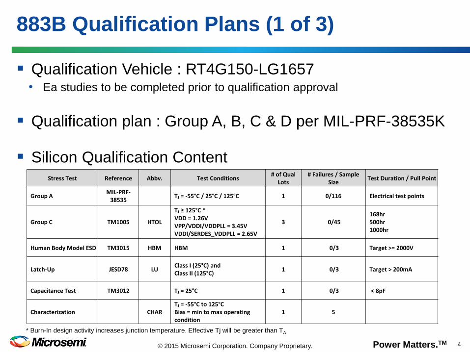
Qualification Vehicle : RT4G150-LG1657 • Ea studies to be completed prior to qualification approval
Qualification plan : Group A, B, C & D per MIL-PRF-38535K
Silicon Qualification Content
883B Qualification Plans (1 of 3)
Stress Test Reference Abbv. Test Conditions # of Qual
Lots # Failures / Sample
Size Test Duration / Pull Point
Group A MIL-PRF-
38535 TJ = -55°C / 25°C / 125°C 1 0/116 Electrical test points
Group C TM1005 HTOL
TJ ≥ 125°C * VDD = 1.26V VPP/VDDI/VDDPLL = 3.45V VDDI/SERDES_VDDPLL = 2.65V
3 0/45 168hr 500hr 1000hr
Human Body Model ESD TM3015 HBM HBM 1 0/3 Target >= 2000V
Latch-Up JESD78 LU Class I (25°C) and Class II (125°C)
1 0/3 Target > 200mA
Capacitance Test TM3012 TJ = 25°C 1 0/3 < 8pF
Characterization CHAR TJ = -55°C to 125°C Bias = min to max operating condition
1 5
* Burn-In design activity increases junction temperature. Effective Tj will be greater than TA

Power Matters.TM 5 © 2015 Microsemi Corporation. Company Proprietary.
Group C • Pre group C
– Endurance test – 220 erase/program cycles to exercise the worst user condition
– Sample margining to record Vt of flash cells
• Group C – 1000 cumulative hours of HTOL
• Post Group C
– Full electrical / functional test
– Margining – monitor Vt shift (charge leakage) on sample flash cells
Group B & Group D • Mechanical and Environmental tests per MIL-PRF-38535K
• Package related tests per MIL-PRF-38535K
883B Qualification Plans (2 of 3)

Power Matters.TM 6 © 2015 Microsemi Corporation. Company Proprietary.
Additional NVM studies planned • Same Flash cell; New Push-Pull bit cell
• Significantly more radiation tolerant structure
• Enhanced HV devices used in programming circuits
883B Qualification Plans (3 of 3)
P-Channel
N-Channel
Pass
Transistor
Simplified view of Push-Pull Cell
Stress Test Reference Abbv. Test Conditions # of Qual Lots # Failures / Sample
Size Test Duration / Pull Point
Non-Volatile Memory Cycling Endurance
JESD22-A117 1-04-12006
NVCE 25 °C and 85°C ≥Tj ≥ 55 °C 3 0/77 220 cycles
Nonvolatile Memory Post-cycling High Temperature Data Retention
JESD22-A117 1-04-12007
PCHTDR Ta = 150°C 3 0/39 Cycles per NVCE
(≥55 °C) / 100 hrs
Non-Volatile Memory Low-Temperature Retention and Read Disturb
JESD22-A117 1-04-12008
LTDR 3 0/38 Cycles per NVCE (25 °C) / 500 hrs
High Temperature Data Retention
JESD22-A117
HTR Ta = 250C 3 0/39 NVM 220 cycles
(25°C), 168 hrs / 0 Fail
Power Matters.TM 7 © 2015 Microsemi Corporation. Company Proprietary.
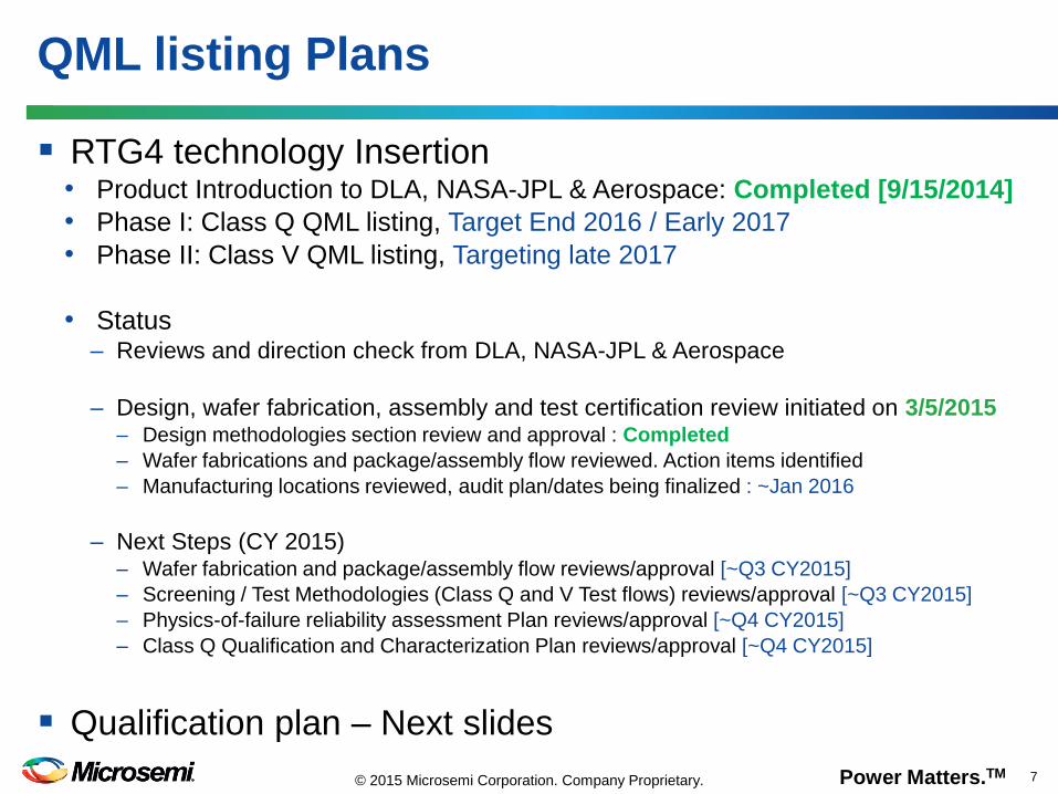
RTG4 technology Insertion • Product Introduction to DLA, NASA-JPL & Aerospace: Completed [9/15/2014]
• Phase I: Class Q QML listing, Target End 2016 / Early 2017
• Phase II: Class V QML listing, Targeting late 2017
• Status – Reviews and direction check from DLA, NASA-JPL & Aerospace
– Design, wafer fabrication, assembly and test certification review initiated on 3/5/2015 – Design methodologies section review and approval : Completed
– Wafer fabrications and package/assembly flow reviewed. Action items identified
– Manufacturing locations reviewed, audit plan/dates being finalized : ~Jan 2016
– Next Steps (CY 2015) – Wafer fabrication and package/assembly flow reviews/approval [~Q3 CY2015]
– Screening / Test Methodologies (Class Q and V Test flows) reviews/approval [~Q3 CY2015]
– Physics-of-failure reliability assessment Plan reviews/approval [~Q4 CY2015]
– Class Q Qualification and Characterization Plan reviews/approval [~Q4 CY2015]
Qualification plan – Next slides
QML listing Plans

Power Matters.TM 8 © 2015 Microsemi Corporation. Company Proprietary.
Process units from 3 wafer lots on Class Q Flow (SoC B Flow)
Complete Group A, B, C & D per MIL-PRF-38535
Group C – 1000hrs @ 125°C • 45 units (LTPD 5); Life test samples evenly distributed
from 3 wafer lots
• Assumptions: Ea = 0.7eV, Tj ≥ 125°C
QML – Class Q approval • Complete Technology Insertion Plan reviews, SMD for
Class Q part number only
RTG4 Class Q Qualification – Phase I
Class Q (Microsemi SoC B Flow)
Wafer Sort
Package Assembly (B flow)
Internal Visual (Cond. B)
Serialization (RT only)
Temperature Cycling (10 Cycles)
Constant Acceleration
PIND (RT only)
Seal (Fine/Gross Leak Test)
Binning Circuit
Comm Temp Test
Dynamic Burn-in (160 Hrs @125C)
Post-BI-Test +25C
Final Test -55C
Final Test +125C
100% QA Electrical +25C
Visual Inspection
Power Matters.TM 9 © 2015 Microsemi Corporation. Company Proprietary.
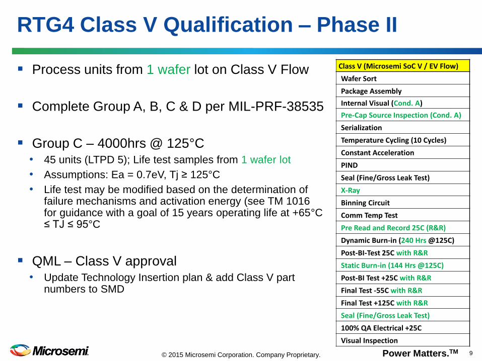
Process units from 1 wafer lot on Class V Flow
Complete Group A, B, C & D per MIL-PRF-38535
Group C – 4000hrs @ 125°C • 45 units (LTPD 5); Life test samples from 1 wafer lot
• Assumptions: Ea = 0.7eV, Tj ≥ 125°C
• Life test may be modified based on the determination of failure mechanisms and activation energy (see TM 1016 for guidance with a goal of 15 years operating life at +65°C ≤ TJ ≤ 95°C
QML – Class V approval • Update Technology Insertion plan & add Class V part
numbers to SMD
RTG4 Class V Qualification – Phase II
Class V (Microsemi SoC V / EV Flow)
Wafer Sort
Package Assembly
Internal Visual (Cond. A)
Pre-Cap Source Inspection (Cond. A)
Serialization
Temperature Cycling (10 Cycles)
Constant Acceleration
PIND
Seal (Fine/Gross Leak Test)
X-Ray
Binning Circuit
Comm Temp Test
Pre Read and Record 25C (R&R)
Dynamic Burn-in (240 Hrs @125C)
Post-BI-Test 25C with R&R
Static Burn-in (144 Hrs @125C)
Post-BI Test +25C with R&R
Final Test -55C with R&R
Final Test +125C with R&R
Seal (Fine/Gross Leak Test)
100% QA Electrical +25C
Visual Inspection

Power Matters.TM 10 © 2015 Microsemi Corporation. Company Proprietary.
Compliant with
MIL-PRF-38535K
Class V production flow adds • 240h dynamic burn-in @ 125 °C
• 144h static burn-in @ 125 °C
• Pre & Post Static and Dynamic BI RnR
RTG4 Production Test Flow (Class Q)
BAKE
Serialization
ASSEMBLYTemp. Cycle / Const.
Accel./PIND / SEAL / Xray
NVM / ATPG /FUNCTIONAL TESTS
Pre Burnin Electrical Test (25C)
START
Dynamic BI160hrs (125C)
Post Burnin Electrical Test (25C)
QA Electrical Test (25C)
CG Attach
QA Electrical Test (25C)
MIL HOT Electrical Test (125C)
MIL Cold Electrical Test (-55C)
NVM / ATPG /FUNCTIONAL TESTS
FINISH
WS
SEAL (fine/gross) Leak Test
Power Matters.TM 11 © 2015 Microsemi Corporation. Company Proprietary.
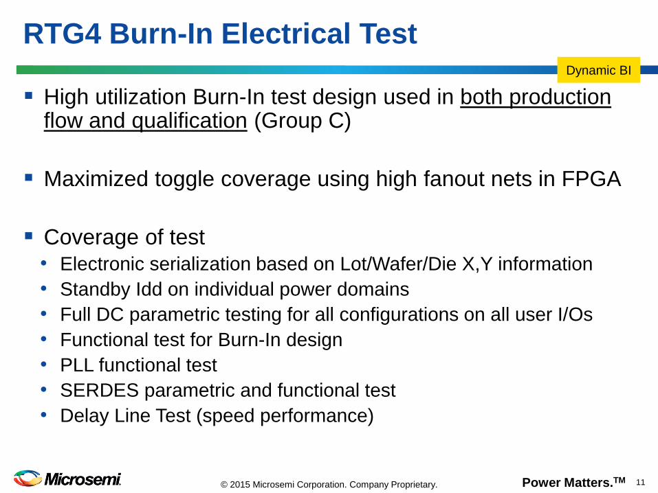
High utilization Burn-In test design used in both production flow and qualification (Group C)
Maximized toggle coverage using high fanout nets in FPGA
Coverage of test
• Electronic serialization based on Lot/Wafer/Die X,Y information
• Standby Idd on individual power domains
• Full DC parametric testing for all configurations on all user I/Os
• Functional test for Burn-In design
• PLL functional test
• SERDES parametric and functional test
• Delay Line Test (speed performance)
RTG4 Burn-In Electrical Test Dynamic BI

Power Matters.TM 12 © 2015 Microsemi Corporation. Company Proprietary.
RTG4 Burn-In Design Overview (1 of 5)
Clock Source • On Chip RCOSC 50MHz clock is fed into all 8 Fabric PLLs of the device
• PLLs deliver the clock signals through global (low skew) networks
UPROM • Checkerboard pattern is stored into the UPROM to maximize output toggle
rate; LFSR generated addresses for read access
• Output read out of UPROM is compared to reference during burn-in
Combo Block • Combinatorial macros available
in the RTG4 library are exercised and compared to reference during burn-in
Register & Latch Block • Sequential macros available in
the RTG4 library are exercised and compared to reference during burn-in.
Combinatorial Macro Block
10 bits
3 bits
7 bits
16 bit CRC
generator
Comparator
9F03
10 bit
counter
BIST
Outputs of
“SR block”
Monitor
Out
Dynamic BI

Power Matters.TM 13 © 2015 Microsemi Corporation. Company Proprietary.
Embedded SRAM blocks • Full R/W toggle coverage on all 209 fabric LSRAM and 210 uRAM blocks
• Dual Port / Two Port configurations ; Maximum width configurations (x18)
• Built-in BIST to monitor functionality during Burn-In
RTG4 Burn-In Design Overview (2 of 5)
Pattern / Address
Generator (Port 1)
Pattern / Address
Generator (Port 2)
Control Signal
Generator
(WEN / BLK / CLK)
Comparator
monitor
Pattern / Address
Generator (Port 1)
Pattern / Address
Generator (Port 2)
Control Signal
Generator
(WEN / BLK / CLK)
Comparator
monitor
Pattern / Address
Generator (Port 1)
Pattern / Address
Generator (Port 2)
Control Signal
Generator
(WEN / BLK / CLK)
1 2
RAM
OUT
Comparator
monitor
MONITOR
1 2
RAM
OUT
1 2
RAM
OUT
Dynamic BI

Power Matters.TM 14 © 2015 Microsemi Corporation. Company Proprietary.
Shift Register Block • Scalable block to maximize core
utilization
• Controlled SSR
IO Block • Scalable block for maximizing I/O
utilization
• Controlled SSO
Math Block • Full toggle coverage on all 462
fabric Mathblocks
• Maximum width configuration
RTG4 Burn-In Design Overview (3 of 5)
MonitorPattern
Generator
Shift Register
Block
Serial
Pattern
Checker
Clock
Out0
1
S
S
0
1
S
S
Output Enable
Pattern In
Reset
Q
QSET
CLR
D0
1
S
S
Q
QSET
CLR
D
Q
QSET
CLR
D
Q
QSET
CLR
D
Math Block
Math Block
Pattern Generator Comparator Monitor
Dynamic BI

Power Matters.TM 15 © 2015 Microsemi Corporation. Company Proprietary.
Oscillator Block (Delay Lines) • Free running ring oscillator circuits to monitor silicon performance pre & post
Burn-In
• Utilizes FPGA resources (Combinatorial, routing tracks and Flash cells)
• Identical paths placed across the chip (6 locations) to capture on-chip variation
• Both Intra and Inter Cluster routing resources exercised
RTG4 Burn-In Design Overview (4 of 5)
OSC_EN
OSC_IN
OSC_OUT
24 stages
Dynamic BI

Power Matters.TM 16 © 2015 Microsemi Corporation. Company Proprietary.
SERDES Block • 100% SERDES blocks utilized (24 lanes)
• Provisions for internal loopback mode in EPCS mode
RTG4 Burn-In Design Overview (5 of 5)
Un
der Evalu
ation
TXDP
TXDN
RXDP
RXDN
Dynamic BI
Power Matters.TM 17 © 2015 Microsemi Corporation. Company Proprietary.
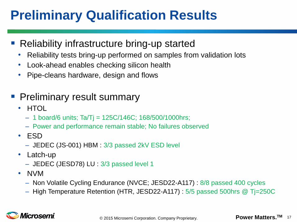
Reliability infrastructure bring-up started • Reliability tests bring-up performed on samples from validation lots
• Look-ahead enables checking silicon health
• Pipe-cleans hardware, design and flows
Preliminary result summary • HTOL
– 1 board/6 units; Ta/Tj = 125C/146C; 168/500/1000hrs;
– Power and performance remain stable; No failures observed
• ESD
– JEDEC (JS-001) HBM : 3/3 passed 2kV ESD level
• Latch-up
– JEDEC (JESD78) LU : 3/3 passed level 1
• NVM
– Non Volatile Cycling Endurance (NVCE; JESD22-A117) : 8/8 passed 400 cycles
– High Temperature Retention (HTR, JESD22-A117) : 5/5 passed 500hrs @ Tj=250C
Preliminary Qualification Results

Power Matters.TM 18 © 2015 Microsemi Corporation. Company Proprietary.
Qualification plans defined to comply with MIL-PRF-38535K/MIL-STD-883B
Initial reliability assessment on samples silicon shows great silicon health
QML listing plans defined • Technology insertion ongoing with DLA, NASA-JPL & Aerospace
• Qualification : Action plan defined; Review and ratification in progress
Timeline • 883 class B qualification completion : Fist Half 2016
• QML class Q classification : Target End 2016 / Early 2017
• QML class V classification : Target late 2017
RTG4 Reliability and Qualification Summary
Power Matters.TM 19 © 2015 Microsemi Corporation. Company Proprietary.
Microsemi Corporation (MSCC) offers a comprehensive portfolio of semiconductor and system solutions for
communications, defense & security, aerospace and industrial markets. Products include high-performance and radiation-
hardened analog mixed-signal integrated circuits, FPGAs, SoCs and ASICs; power management products; timing and
synchronization devices and precise time solutions, setting the world's standard for time; voice processing devices; RF
solutions; discrete components; security technologies and scalable anti-tamper products; Ethernet solutions; Power-over-
Ethernet ICs and midspans; as well as custom design capabilities and services. Microsemi is headquartered in Aliso
Viejo, Calif., and has approximately 3,600 employees globally. Learn more at www.microsemi.com.
©2015 Microsemi Corporation. All rights reserved. Microsemi and the Microsemi logo are registered trademarks of Microsemi Corporation. All other
trademarks and service marks are the property of their respective owners.
Microsemi makes no warranty, representation, or guarantee regarding the information contained herein or the suitability of its products and services for any particular
purpose, nor does Microsemi assume any liability whatsoever arising out of the application or use of any product or circuit. The products sold hereunder and any other
products sold by Microsemi have been subject to limited testing and should not be used in conjunction with mission-critical equipment or applications. Any
performance specifications are believed to be reliable but are not verified, and Buyer must conduct and complete all performance and other testing of the products,
alone and together with, or installed in, any end-products. Buyer shall not rely on any data and performance specifications or parameters provided by Microsemi. It is
the Buyer’s responsibility to independently determine suitability of any products and to test and verify the same. The information provided by Microsemi hereunder is
provided “as is, where is” and with all faults, and the entire risk associated with such information is entirely with the Buyer. Microsemi does not grant, explicitly or
implicitly, to any party any patent rights, licenses, or any other IP rights, whether with regard to such information itself or anything described by such information.
Information provided in this document is proprietary to Microsemi, and Microsemi reserves the right to make any changes to the information in this document or to any
products and services at any time without notice.
Microsemi Corporate Headquarters
One Enterprise, Aliso Viejo, CA 92656 USA
Within the USA: +1 (800) 713-4113
Outside the USA: +1 (949) 380-6100
Sales: +1 (949) 380-6136
Fax: +1 (949) 215-4996
email: [email protected]
Thank You
Top Related