


Languages
Pages
Legal

RIDL visit-1BEB 04/18/23
MIT Lincoln Laboratory
Orthogonal-Transfer Charge-Coupled Devices and Low-Noise Charge-Coupled Devices Readout Circuits*
Barry E. Burke
*The MIT Lincoln Laboratory portion of this work was performed under a Collaboration Agreement between MIT Lincoln Laboratory and The University of Hawaii, Institute for Astronomy (IfA). Opinions, interpretations, conclusions, and recommendations are those of the authors, and do not necessarily represent the view of the United States Government.
MIT Lincoln LaboratoryRIDL visit-2
BEB 04/18/23
Outline
• Review of Orthogonal-Transfer Charge-Coupled Devices (OTCCD)
• Development of the orthogonal transfer array (OTA)
• Low-noise CCD readout circuits
• Summary
MIT Lincoln LaboratoryRIDL visit-3
BEB 04/18/23
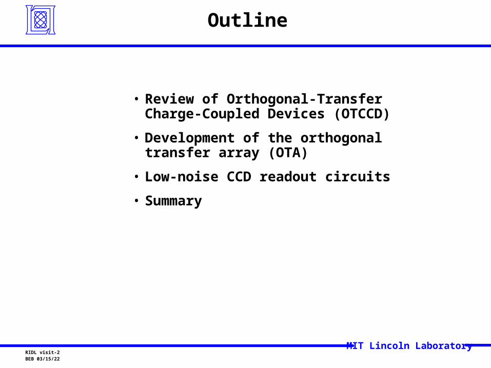
Conventional vs. Orthogonal-Transfer CCDs
MIT Lincoln LaboratoryRIDL visit-4
BEB 04/18/23
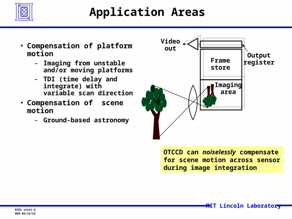
Application Areas
• Compensation of platform motion– Imaging from unstable
and/or moving platforms– TDI (time delay and integrate)
with variable scan direction
• Compensation of scene motion– Ground-based astronomy
Outputregister
Videoout
Framestore
Imagingarea
OTCCD can noiselessly compensatefor scene motion across sensorduring image integration
MIT Lincoln LaboratoryRIDL visit-5
BEB 04/18/23
Application of OTCCDs in Astronomy
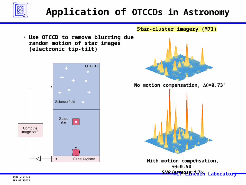
Star-cluster imagery (M71)
With motion compensation, =0.50”SNR increase: 1.7
• Use OTCCD to remove blurring due random motion of star images (electronic tip-tilt)
No motion compensation, =0.73"
MIT Lincoln LaboratoryRIDL visit-6
BEB 04/18/23
Outline
• Review of Orthogonal-Transfer Charge-Coupled Devices (OTCCD)
• Development of the orthogonal transfer array (OTA)
• Low-noise CCD readout circuits• Summary
MIT Lincoln LaboratoryRIDL visit-7
BEB 04/18/23
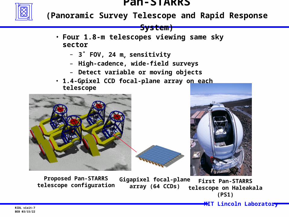
Pan-STARRS(Panoramic Survey Telescope and Rapid Response System)
Proposed Pan-STARRStelescope configuration
Gigapixel focal-planearray (64 CCDs)
• Four 1.8-m telescopes viewing same sky sector– 3˚ FOV, 24 mv sensitivity– High-cadence, wide-field surveys– Detect variable or moving objects
• 1.4-Gpixel CCD focal-plane array on each telescope
First Pan-STARRStelescope on Haleakala
(PS1)
MIT Lincoln LaboratoryRIDL visit-8
BEB 04/18/23
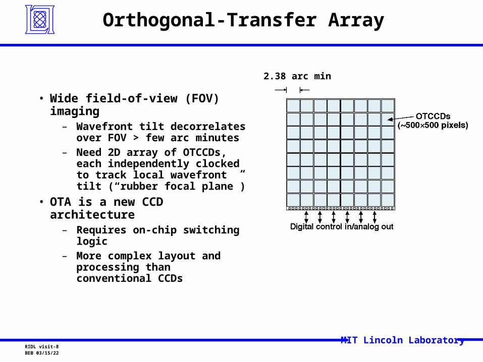
Orthogonal-Transfer Array
• Wide field-of-view (FOV) imaging– Wavefront tilt decorrelates over
FOV > few arc minutes– Need 2D array of OTCCDs, each
independently clocked to track local wavefront tilt (“rubber focal plane”)
• OTA is a new CCD architecture– Requires on-chip switching logic– More complex layout and
processing than conventional CCDs
2.38 arc min
MIT Lincoln LaboratoryRIDL visit-9
BEB 04/18/23
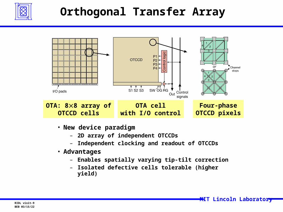
Orthogonal Transfer Array
• New device paradigm– 2D array of independent OTCCDs– Independent clocking and readout of OTCCDs
• Advantages– Enables spatially varying tip-tilt correction– Isolated defective cells tolerable (higher yield)
OTA: 88 array ofOTCCD cells
OTA cellwith I/O control
Four-phaseOTCCD pixels
MIT Lincoln LaboratoryRIDL visit-10BEB 04/18/23
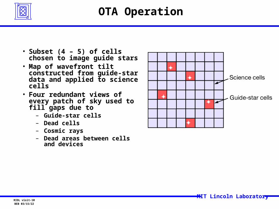
OTA Operation
• Subset (4 – 5) of cells chosen to image guide stars
• Map of wavefront tilt constructed from guide-star data and applied to science cells
• Four redundant views of every patch of sky used to fill gaps due to– Guide-star cells– Dead cells– Cosmic rays– Dead areas between cells and
devices
MIT Lincoln LaboratoryRIDL visit-11BEB 04/18/23
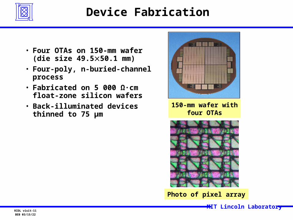
Device Fabrication
• Four OTAs on 150-mm wafer (die size 49.550.1 mm)
• Four-poly, n-buried-channel process
• Fabricated on 5 000 Ω·cm float-zone silicon wafers
• Back-illuminated devices thinned to 75 µm
150-mm wafer withfour OTAs
Photo of pixel array
MIT Lincoln LaboratoryRIDL visit-12BEB 04/18/23
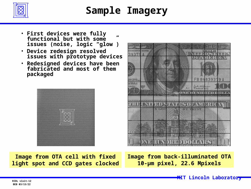
Sample Imagery
• First devices were fully functional but with some issues (noise, logic “glow”)
• Device redesign resolved issues with prototype devices
• Redesigned devices have been fabricated and most of them packaged
Image from back-illuminated OTA10-µm pixel, 22.6 Mpixels
Image from OTA cell with fixedlight spot and CCD gates clocked
MIT Lincoln LaboratoryRIDL visit-13BEB 04/18/23
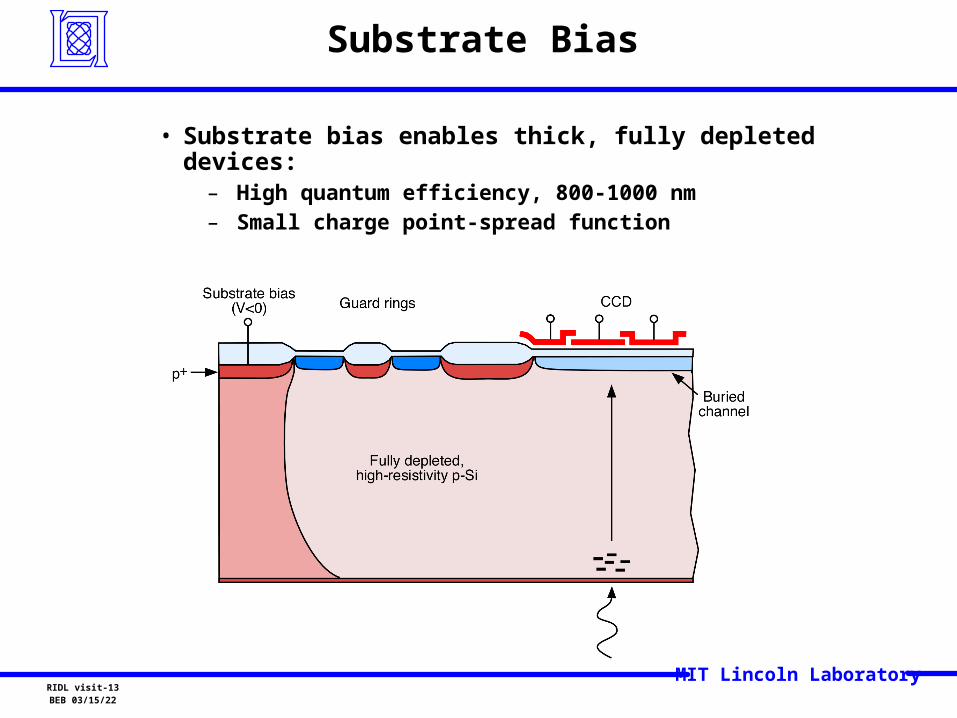
Substrate Bias
• Substrate bias enables thick, fully depleted devices:– High quantum efficiency, 800-1000 nm– Small charge point-spread function
MIT Lincoln LaboratoryRIDL visit-14BEB 04/18/23
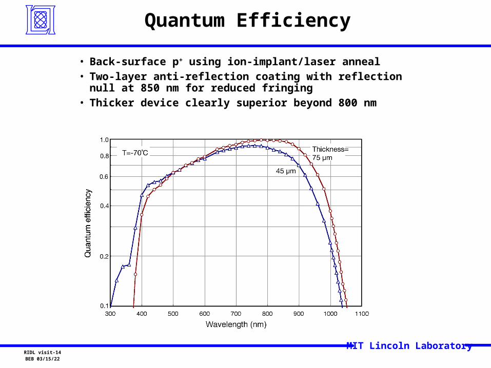
Quantum Efficiency
• Back-surface p+ using ion-implant/laser anneal• Two-layer anti-reflection coating with reflection null at
850 nm for reduced fringing• Thicker device clearly superior beyond 800 nm
MIT Lincoln LaboratoryRIDL visit-15BEB 04/18/23
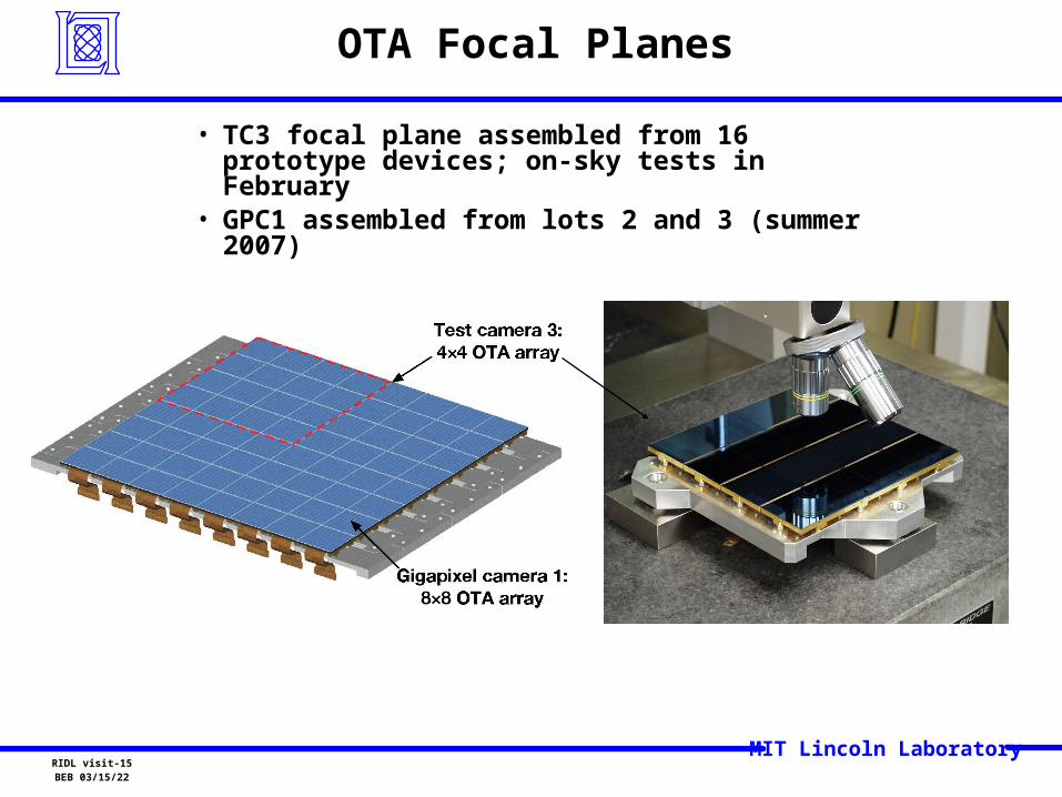
OTA Focal Planes
• TC3 focal plane assembled from 16 prototype devices; on-sky tests in February
• GPC1 assembled from lots 2 and 3 (summer 2007)
MIT Lincoln LaboratoryRIDL visit-16BEB 04/18/23
Outline
• Review of Orthogonal-Transfer Charge-Coupled Devices (OTCCD)
• Development of the orthogonal transfer array (OTA)
• Low-noise CCD readout circuits• Summary
MIT Lincoln LaboratoryRIDL visit-17BEB 04/18/23
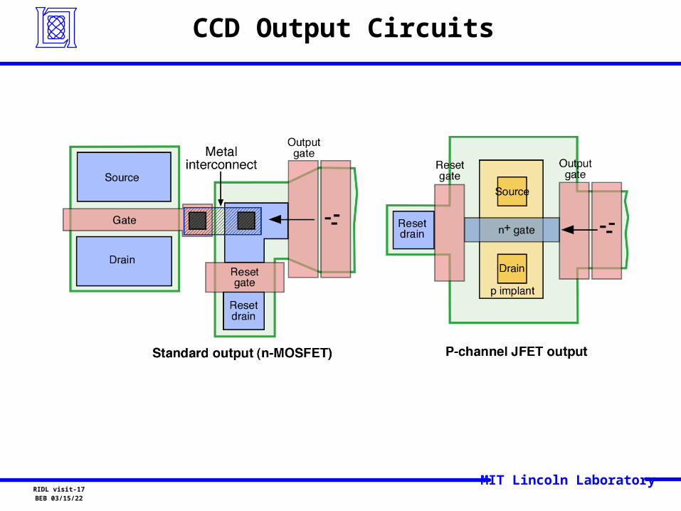
CCD Output Circuits
MIT Lincoln LaboratoryRIDL visit-18BEB 04/18/23
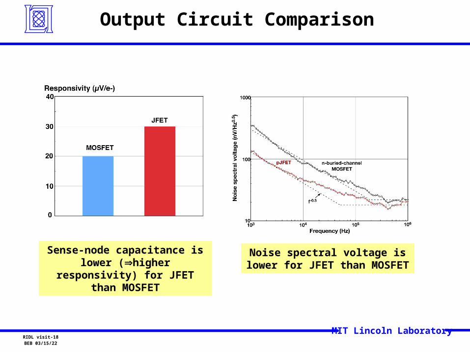
Output Circuit Comparison
Sense-node capacitance is lower (higher responsivity) for JFET
than MOSFET
Noise spectral voltage is lower for JFET than MOSFET
MIT Lincoln LaboratoryRIDL visit-19BEB 04/18/23
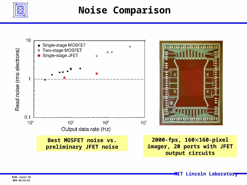
Noise Comparison
Best MOSFET noise vs. preliminary JFET noise
2000-fps, 160160-pixel imager, 20 ports with JFET output circuits
MIT Lincoln LaboratoryRIDL visit-20BEB 04/18/23
Summary
• OTCCD developed for astronomical applications but has a potentially much broader range of uses
• OTA development for Pan-STARRS is new OTCCD concept, also with other applications
• Recent work with JFETs shows noise levels better than BCMOSFETs and nearing 1 e-
Top Related