


Languages
Pages
Legal

Dr. Ahmed Bassyouni 1
Dr. Ahmed M. BassyouniDr. Ahmed M. Bassyouni Research ProfessorResearch Professor
Electrical and Computer Engineering DepartmentElectrical and Computer Engineering DepartmentBoise State University, IdahoBoise State University, Idaho
On-chip RF On-chip RF Transceiver CircuitsTransceiver Circuits
Dr. Ahmed Bassyouni 2
A Design Approach for Sub-micronCMOS Low Noise Amplifier
Electrical Engineering Department
Boise State University, Boise Idaho
Dr. Ahmed Bassyouni 3
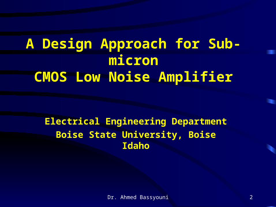
Receiver channel
Dr. Ahmed Bassyouni 4
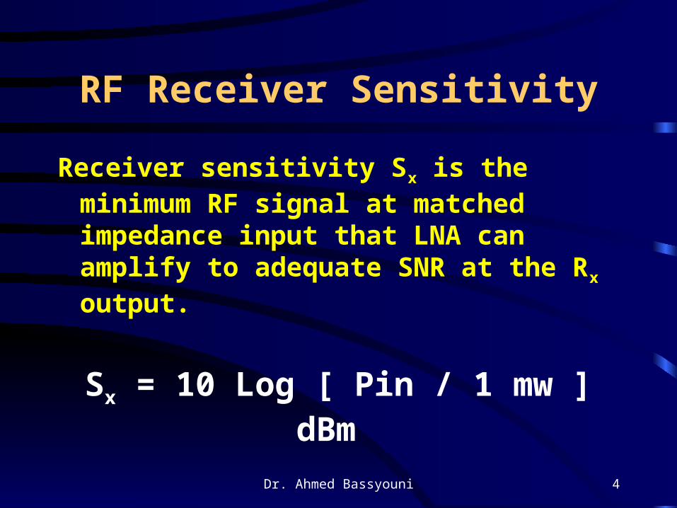
RF Receiver Sensitivity
Receiver sensitivity Sx is the minimum RF signal at matched impedance input that LNA can amplify to adequate SNR at the Rx output.
Sx = 10 Log [ Pin / 1 mw ] dBm
Dr. Ahmed Bassyouni 5
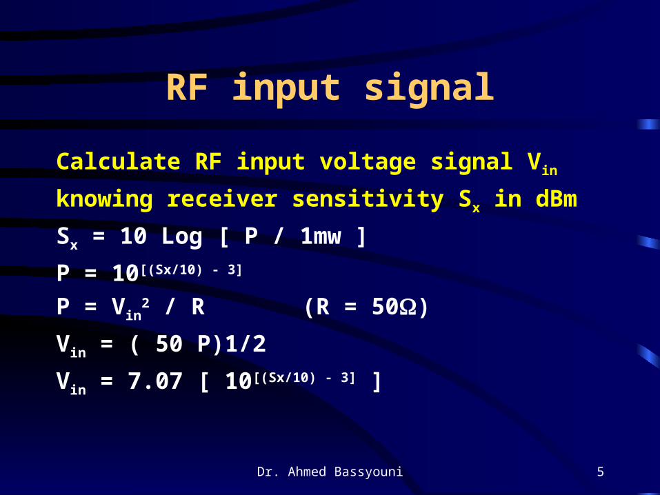
RF input signal
Calculate RF input voltage signal Vin
knowing receiver sensitivity Sx in dBm
Sx = 10 Log [ P / 1mw ]
P = 10[(Sx/10) - 3]
P = Vin2 / R (R = 50)
Vin = ( 50 P)1/2
Vin = 7.07 [ 10[(Sx/10) - 3] ]
Dr. Ahmed Bassyouni 6
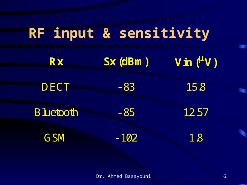
RF input & sensitivity
Rx Sx (dBm) Vin (V)
DECT - 83 15.8
Bluetooth - 85 12.57
GSM - 102 1.8
Dr. Ahmed Bassyouni 7
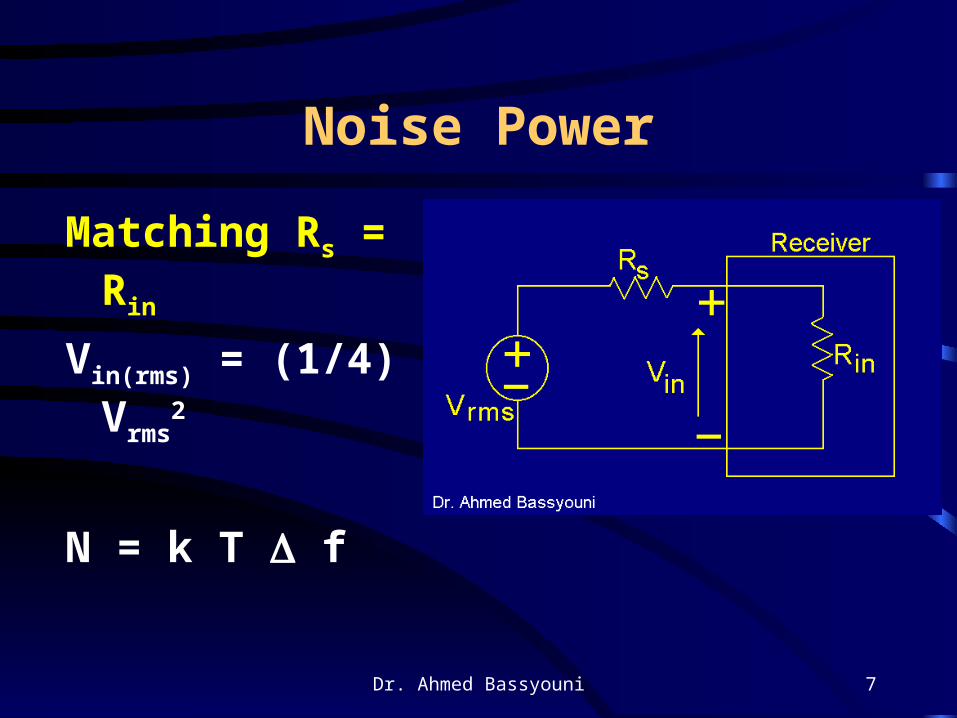
Noise Power
Matching Rs = Rin
Vin(rms) = (1/4) Vrms2
N = k T f
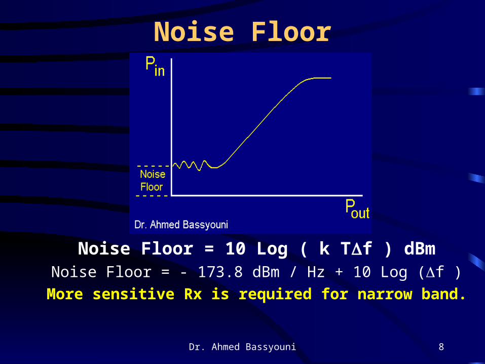
Dr. Ahmed Bassyouni 8
Noise Floor
Noise Floor = 10 Log ( k Tf ) dBmNoise Floor = - 173.8 dBm / Hz + 10 Log (f )
More sensitive Rx is required for narrow band.
Dr. Ahmed Bassyouni 9
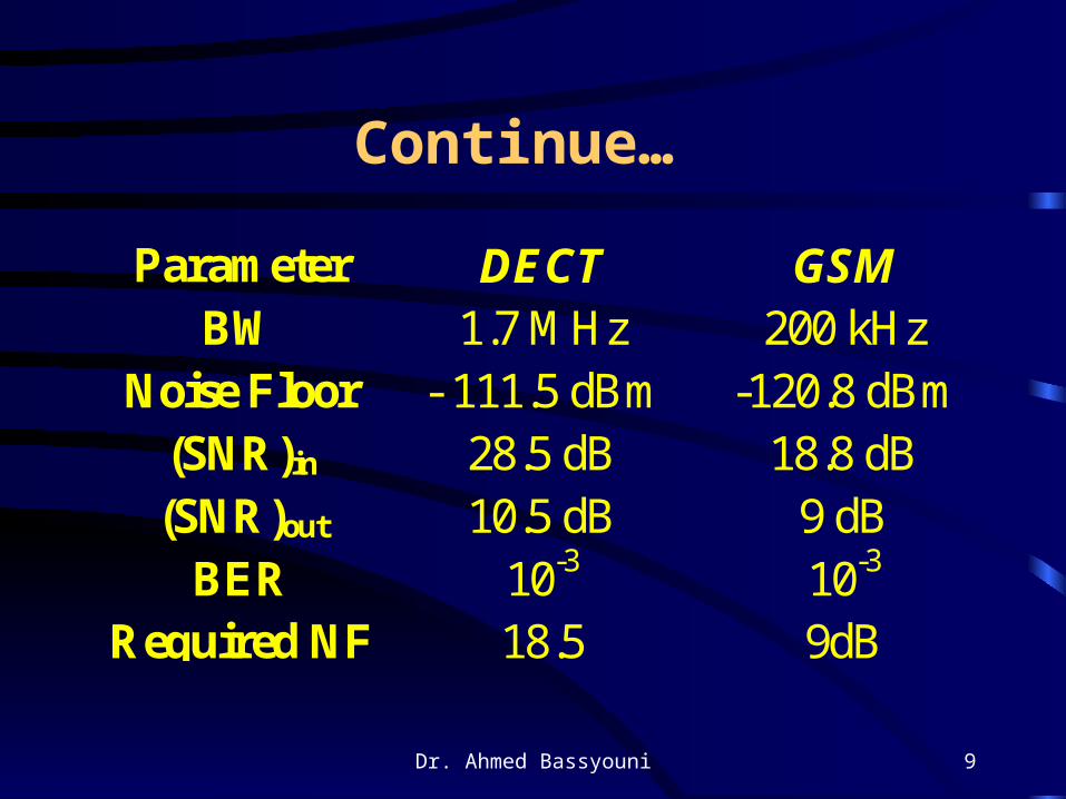
Continue…
Parameter DECT GSMBW 1.7 MHz 200 kHz
Noise Floor - 111.5 dBm -120.8 dBm(SNR)in 28.5 dB 18.8 dB(SNR)out 10.5 dB 9 dB
BER 10-3 10-3
Required NF 18.5 9dB
Dr. Ahmed Bassyouni 10
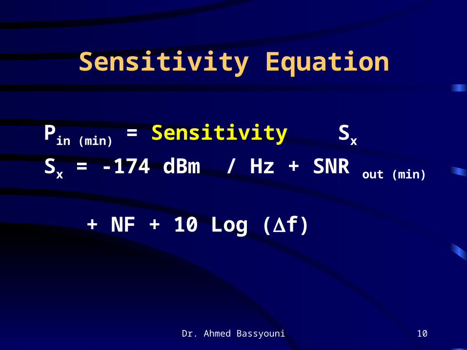
Sensitivity Equation
Pin (min) = Sensitivity Sx
Sx = -174 dBm / Hz + SNR out (min)
+ NF + 10 Log (f)
Dr. Ahmed Bassyouni 11
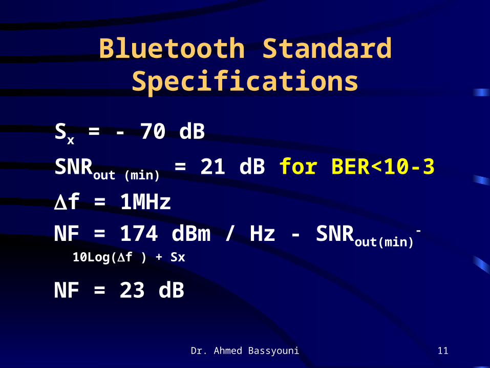
Bluetooth Standard Specifications
Sx = - 70 dB
SNRout (min) = 21 dB for BER<10-3
f = 1MHz
NF = 174 dBm / Hz - SNRout(min)-10Log(f ) + Sx
NF = 23 dB

Dr. Ahmed Bassyouni 12
Noise Figure Definition
Noise Factor F = [ SNRin / SNRout ]
NF = 10 Log F dB
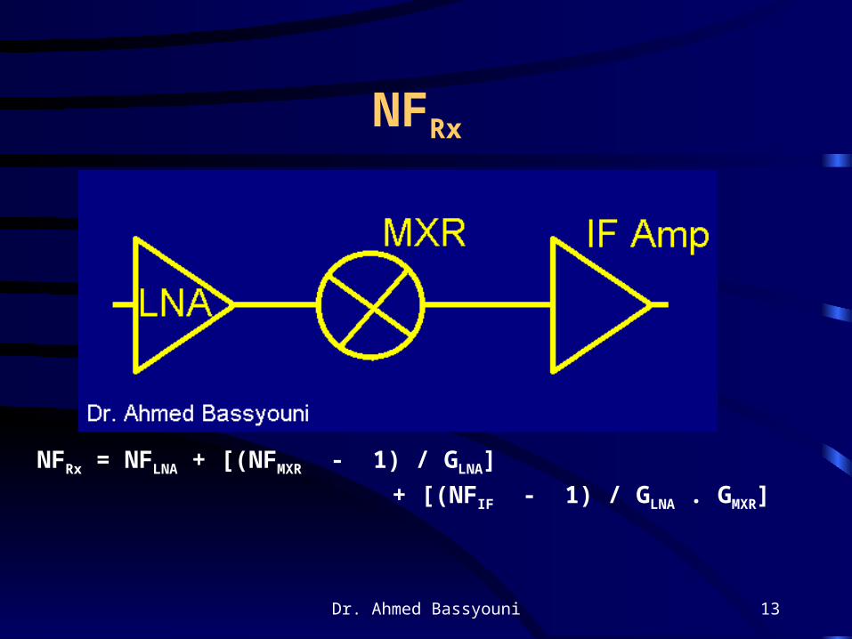
Dr. Ahmed Bassyouni 13
NFRx
NFRx = NFLNA + [(NFMXR - 1) / GLNA]
+ [(NFIF - 1) / GLNA . GMXR]
Dr. Ahmed Bassyouni 14
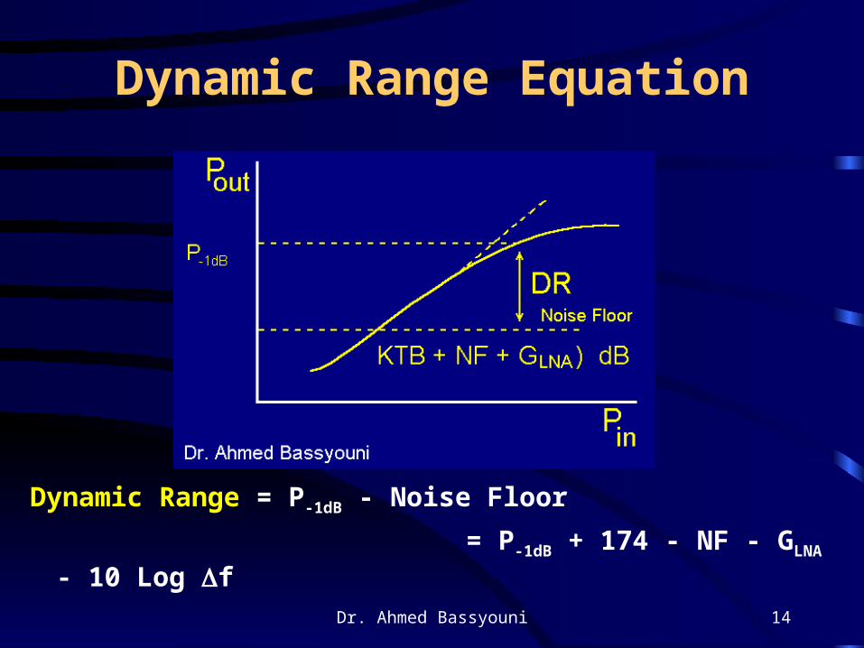
Dynamic Range Equation
Dynamic Range = P-1dB - Noise Floor
= P-1dB + 174 - NF - GLNA - 10 Log f
Dr. Ahmed Bassyouni 15
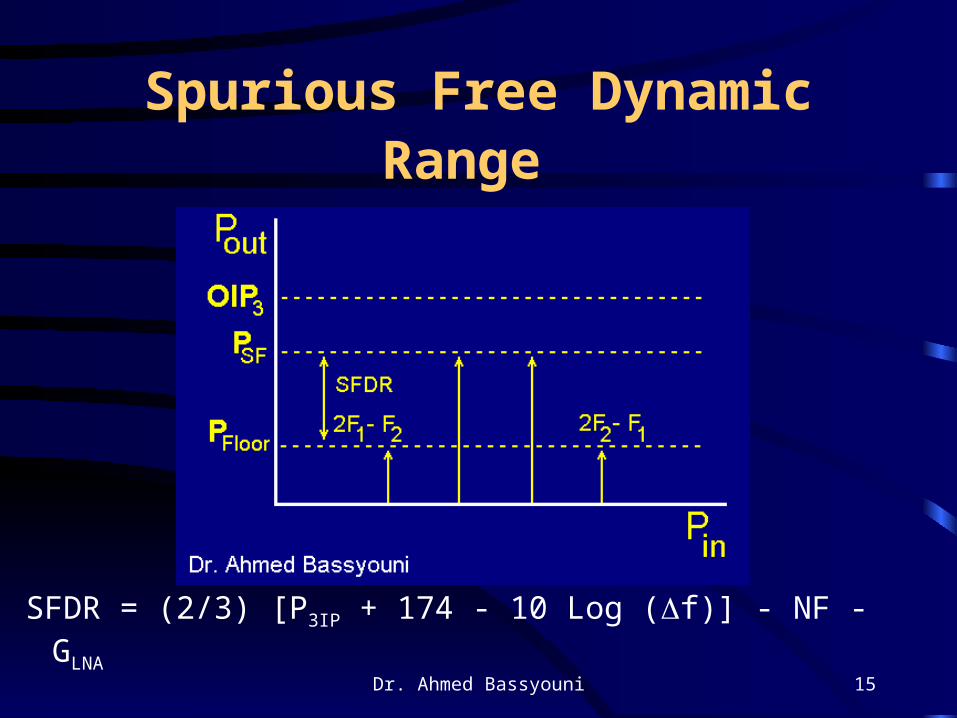
Spurious Free Dynamic Range
SFDR = (2/3) [P3IP + 174 - 10 Log (f)] - NF -GLNA
Dr. Ahmed Bassyouni 16
Linearity Linearity of the receiver determines the
maximum allowable signal level to its input.
Nonlinear system V0 = f (V0)
V0 = a0 + a1 Vi + a2 Vi2 + a3 Vi3
a0 dc……. offset term
a1 Vi……. linear term
a2 Vi2…... quadratic term
a3 Vi3…... 3th order term
Dr. Ahmed Bassyouni 17
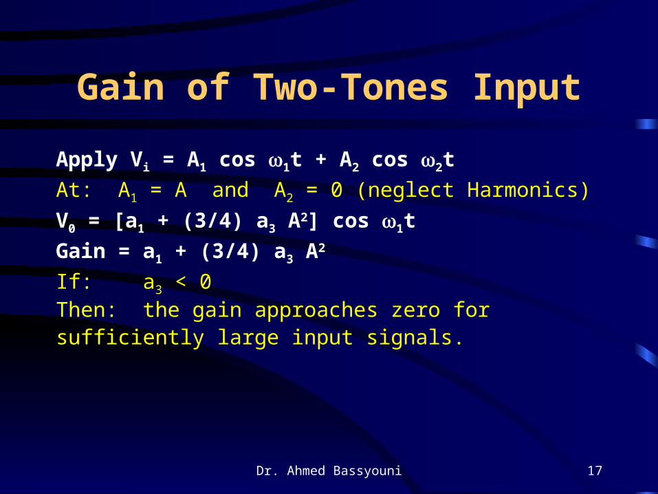
Gain of Two-Tones Input
Apply Vi = A1 cos 1t + A2 cos 2t
At: A1 = A and A2 = 0 (neglect Harmonics)
V0 = [a1 + (3/4) a3 A2] cos 1t
Gain = a1 + (3/4) a3 A2
If: a3 < 0Then: the gain approaches zero for sufficiently large input signals.
Dr. Ahmed Bassyouni 18
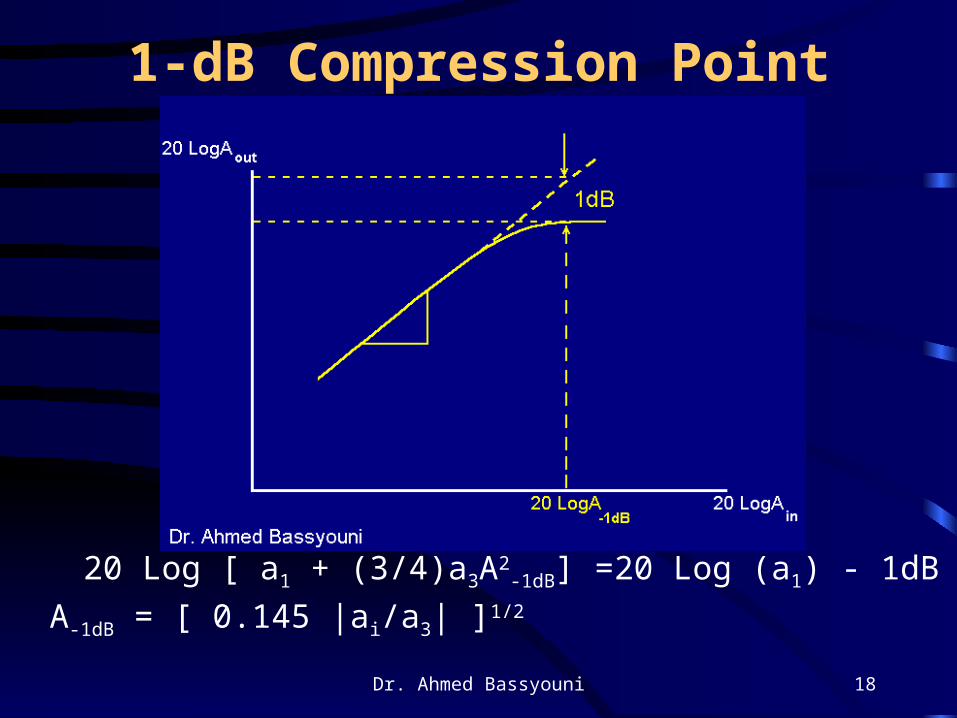
1-dB Compression Point
20 Log [ a1 + (3/4)a3A2-1dB] =20 Log (a1) - 1dB
A-1dB = [ 0.145 |ai/a3| ]1/2
Dr. Ahmed Bassyouni 19
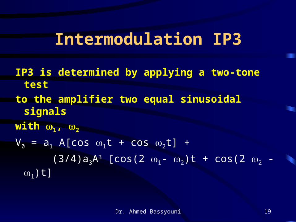
Intermodulation IP3
IP3 is determined by applying a two-tone test
to the amplifier two equal sinusoidal signals
with 1, 2
V0 = a1 A[cos 1t + cos 2t] +
(3/4)a3A3 [cos(2 1- 2)t + cos(2 2 - 1)t]
Dr. Ahmed Bassyouni 20
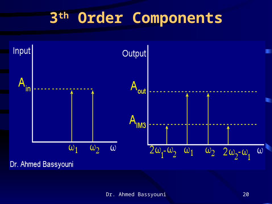
3th Order Components
Dr. Ahmed Bassyouni 21
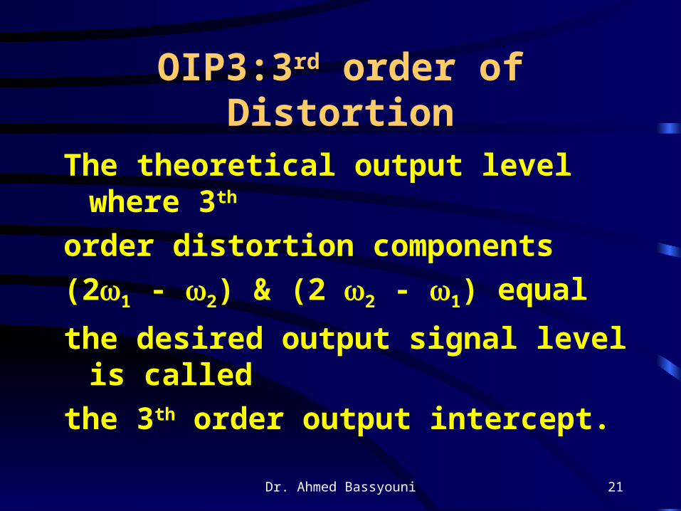
OIP3:3rd order of Distortion
The theoretical output level where 3th
order distortion components
(21 - 2) & (2 2 - 1) equal
the desired output signal level is called
the 3th order output intercept.
Dr. Ahmed Bassyouni 22
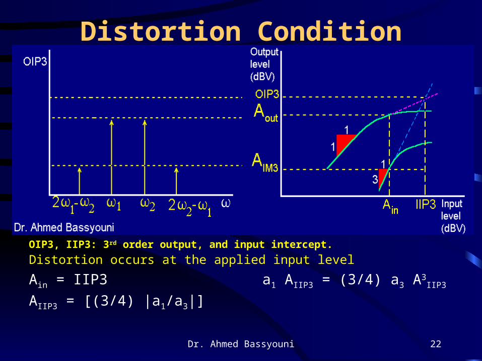
Distortion Condition
OIP3, IIP3: 3rd order output, and input intercept.
Distortion occurs at the applied input level
Ain = IIP3 a1 AIIP3 = (3/4) a3 A3IIP3
AIIP3 = [(3/4) |a1/a3|]
Dr. Ahmed Bassyouni 23
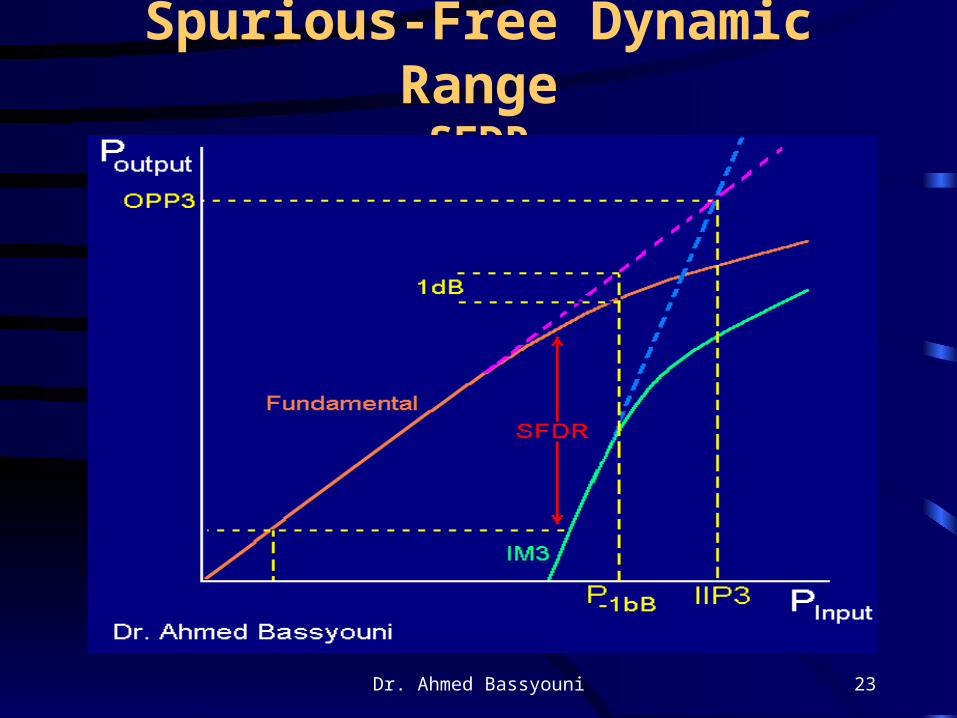
Spurious-Free Dynamic RangeSFDR
Dr. Ahmed Bassyouni 24
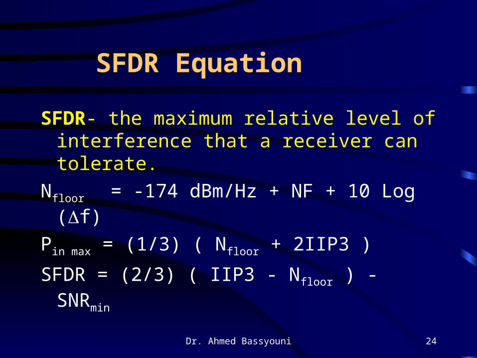
SFDR Equation
SFDR- the maximum relative level of interference that a receiver can tolerate.
Nfloor = -174 dBm/Hz + NF + 10 Log (f)
Pin max = (1/3) ( Nfloor + 2IIP3 )
SFDR = (2/3) ( IIP3 - Nfloor ) - SNRmin
Dr. Ahmed Bassyouni 25
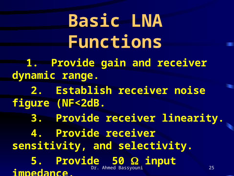
Basic LNA Functions
1. Provide gain and receiver dynamic range.
2. Establish receiver noise figure (NF<2dB.
3. Provide receiver linearity.
4. Provide receiver sensitivity, and selectivity.
5. Provide 50 input impedance.
6. Minimum power dissipation.
7. Provide receiver stability.
Dr. Ahmed Bassyouni 26
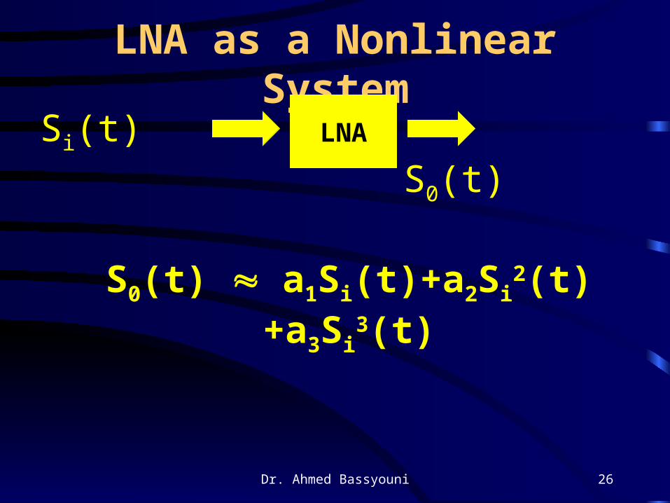
LNA as a Nonlinear System
Si(t) S0(t)
S0(t) a1Si(t)+a2Si2(t)+a3Si
3(t)
LNA
Dr. Ahmed Bassyouni 27
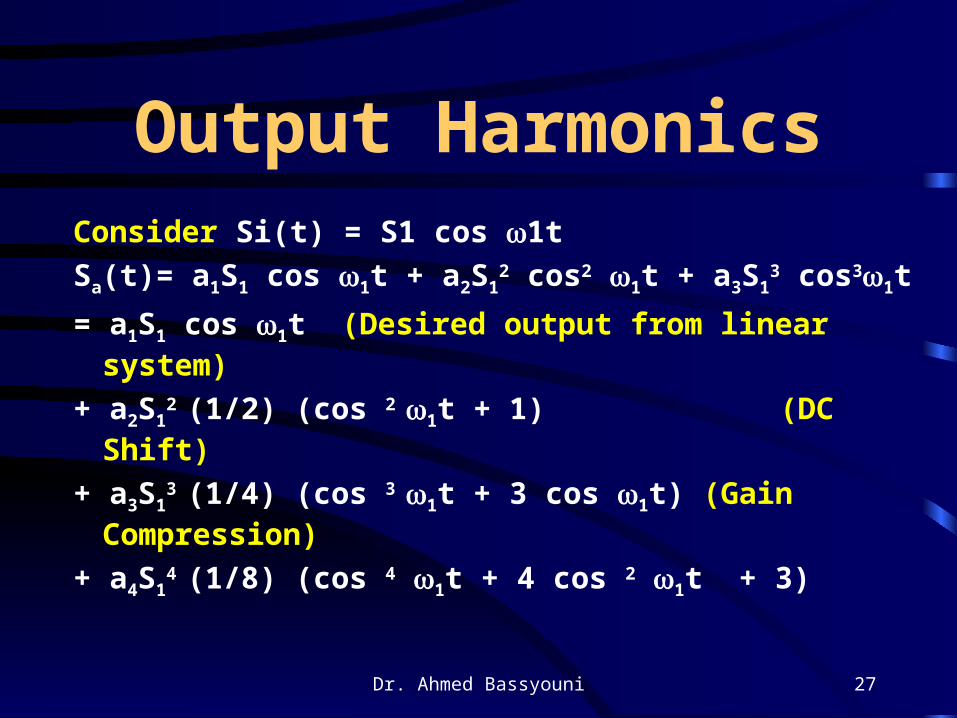
Output HarmonicsConsider Si(t) = S1 cos 1t
Sa(t)= a1S1 cos 1t + a2S12 cos2 1t + a3S1
3 cos31t
= a1S1 cos 1t (Desired output from linear system)
+ a2S12 (1/2) (cos 2 1t + 1) (DC Shift)
+ a3S13 (1/4) (cos 3 1t + 3 cos 1t) (Gain Compression)
+ a4S14 (1/8) (cos 4 1t + 4 cos 2 1t + 3)
Dr. Ahmed Bassyouni 28
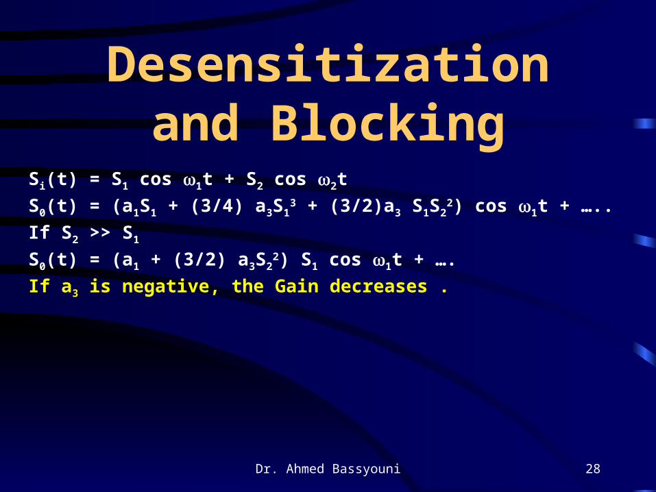
Desensitization and Blocking
Si(t) = S1 cos 1t + S2 cos 2t
S0(t) = (a1S1 + (3/4) a3S13 + (3/2)a3 S1S2
2) cos 1t + …..
If S2 >> S1
S0(t) = (a1 + (3/2) a3S22) S1 cos 1t + ….
If a3 is negative, the Gain decreases .
Dr. Ahmed Bassyouni 29
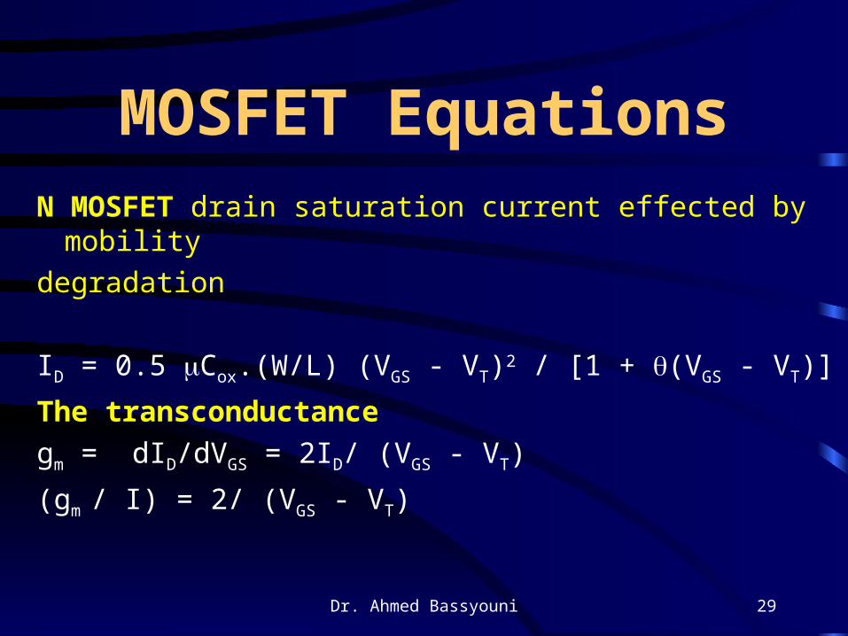
MOSFET EquationsN MOSFET drain saturation current effected by mobility
degradation
ID = 0.5 Cox.(W/L) (VGS - VT)2 / [1 + (VGS - VT)]
The transconductance
gm = dID/dVGS = 2ID/ (VGS - VT)
(gm / I) = 2/ (VGS - VT)
Dr. Ahmed Bassyouni 30
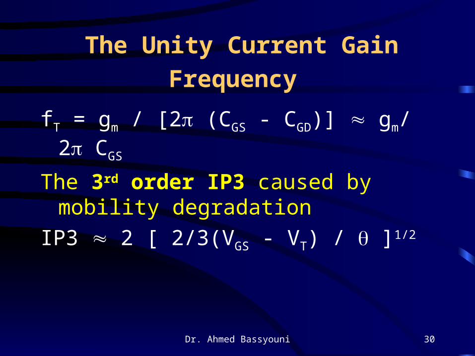
The Unity Current Gain Frequency
fT = gm / [2 (CGS - CGD)] gm/ 2 CGS
The 3rd order IP3 caused by mobility degradation
IP3 2 [ 2/3(VGS - VT) / ]1/2
Dr. Ahmed Bassyouni 31
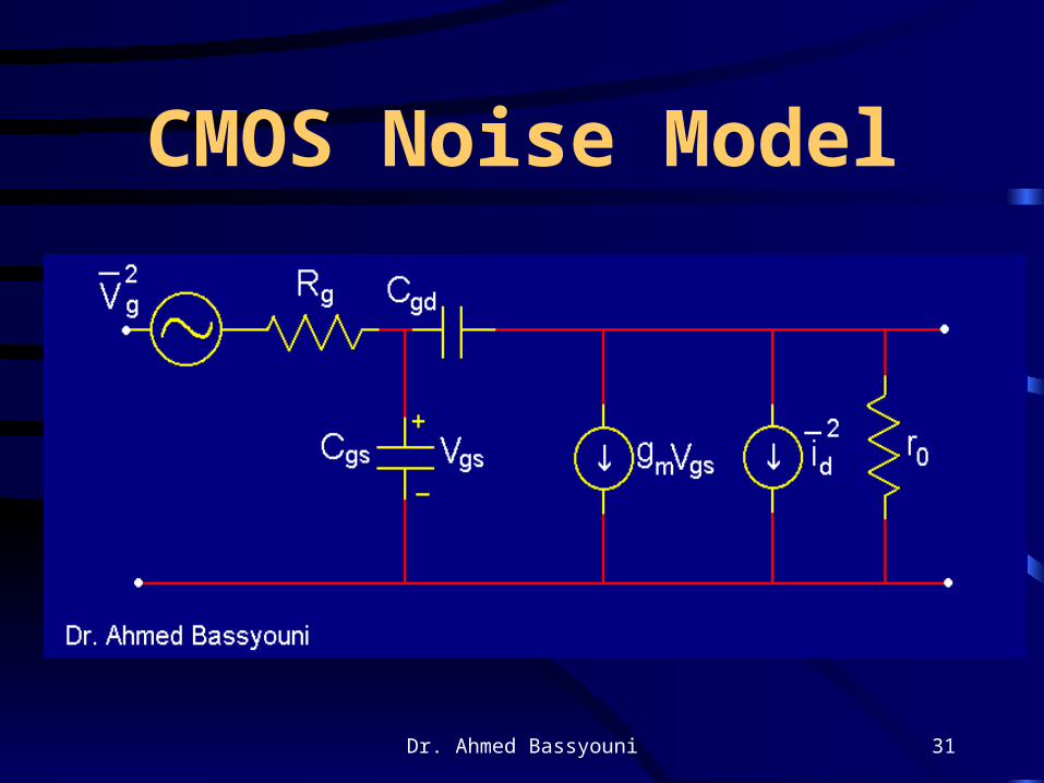
CMOS Noise Model
Dr. Ahmed Bassyouni 32
CMOS Noise Model(Id
2/f) = 4kT gdo + (k/f) (gm2 / WLCox
2)
Vg2 = 4kT Rg , Rg = (1/ 5gdo)
= a bias dependant factor.
(2/3) < <1 (Long channel) >1 (Short Channel)
gdo zero-bias drain conductance.
gate noise-factor.
= 4/3 (Long channel) =2 (Short Channel)
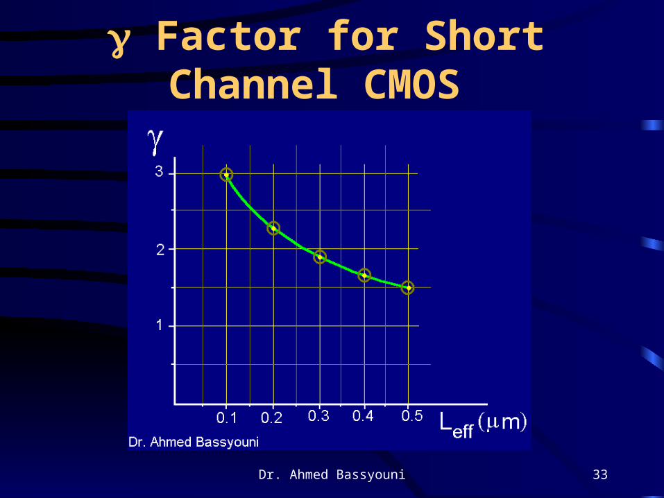
Dr. Ahmed Bassyouni 33
Factor for Short Channel CMOS
Dr. Ahmed Bassyouni 34
LNA Design Considerations
• The Gain is typically 10 dB < Gain <10 dB Sufficient gain to minimize
the influence of noise, but not too
high, otherwise interfering signals will exceed mixer’s linearity.
• NF must be as little as possible, up to the application. Bluetooth NF < 4 dB.
• Good linearity to accommodate large signals without distraction.
• Zin = 50 to ensure high quality gain-frequency for narrow band.
• Minimum power dissipation (can be achieved with scaled CMOS).
Dr. Ahmed Bassyouni 35
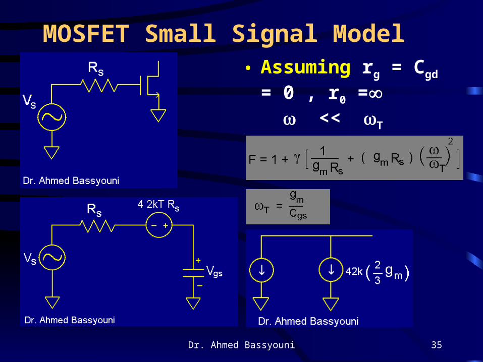
MOSFET Small Signal Model • Assuming rg = Cgd = 0 ,
r0 = << T
• Noise Factor
Dr. Ahmed Bassyouni 36
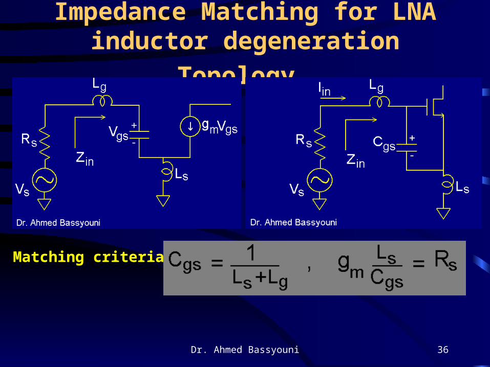
Impedance Matching for LNA
inductor degeneration Topology
Matching criteria
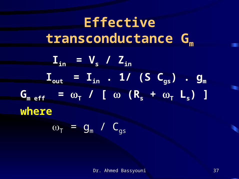
Dr. Ahmed Bassyouni 37
Effective transconductance Gm
Iin = Vs / Zin
Iout = Iin . 1/ (S Cgs) . gm
Gm eff = T / [ (Rs + T Ls) ]
where
T = gm / Cgs
Dr. Ahmed Bassyouni 38
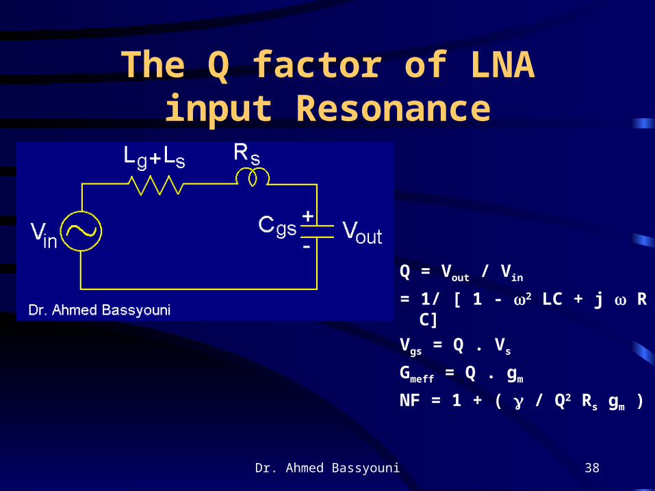
The Q factor of LNA input Resonance
Q = Vout / Vin
= 1/ [ 1 - 2 LC + j R C]
Vgs = Q . Vs
Gmeff = Q . gm
NF = 1 + ( / Q2 Rs gm )
Dr. Ahmed Bassyouni 39
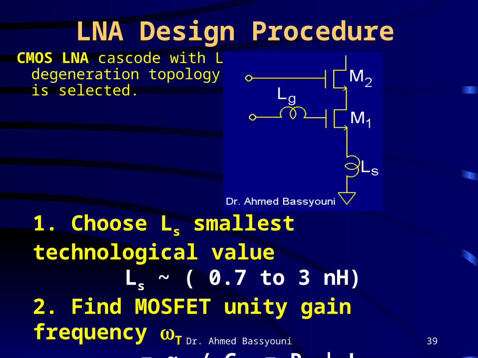
LNA Design ProcedureCMOS LNA cascode with
L degeneration topology is selected.
1. Choose Ls smallest technological value Ls ~ ( 0.7 to 3 nH)
2. Find MOSFET unity gain frequency T
T = gm / Cgs = Rs | Ls
Dr. Ahmed Bassyouni 40
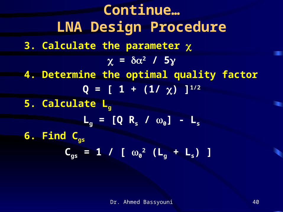
Continue…LNA Design Procedure
3. Calculate the parameter = 2 / 5
4. Determine the optimal quality factor
Q = [ 1 + (1/ ) ]1/2
5. Calculate Lg
Lg = [Q Rs / 0] - Ls
6. Find Cgs
Cgs = 1 / [ 02 (Lg + Ls) ]
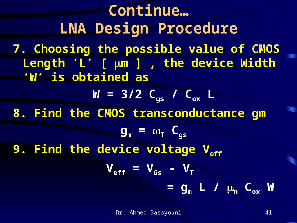
Dr. Ahmed Bassyouni 41
Continue…LNA Design Procedure
7. Choosing the possible value of CMOS Length ‘L’ [ m ] , the device Width ‘W’ is obtained as
W = 3/2 Cgs / Cox L
8. Find the CMOS transconductance gm
gm = T Cgs
9. Find the device voltage Veff
Veff = VGs - VT
= gm L / n Cox W

Dr. Ahmed Bassyouni 42
Continue…LNA Design Procedure
10 . Find the device drain current
ID = 0.5 gm Veff
11. Calculate the noise factor F
Dr. Ahmed Bassyouni 43
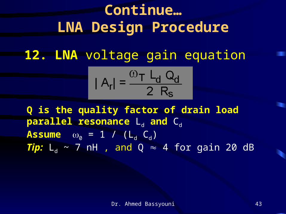
Continue…LNA Design Procedure
12. LNA voltage gain equation
Q is the quality factor of drain load parallel resonance Ld and Cd
Assume 0 = 1 / (Ld Cd)Tip: Ld ~ 7 nH , and Q 4 for gain 20 dB
Dr. Ahmed Bassyouni 44
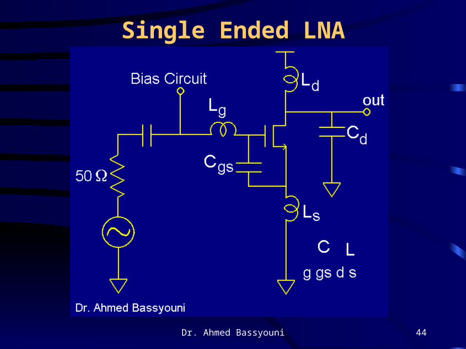
Single Ended LNA
Dr. Ahmed Bassyouni 45
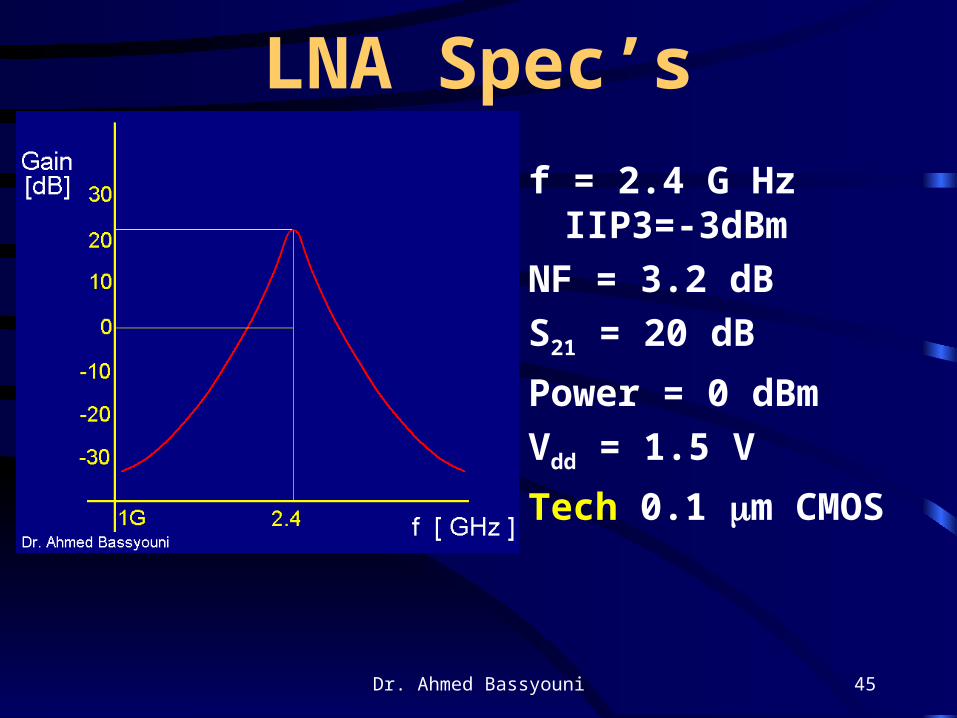
LNA Spec’s
f = 2.4 G Hz IIP3=-3dBm
NF = 3.2 dB
S21 = 20 dB
Power = 0 dBm
Vdd = 1.5 V
Tech 0.1 m CMOS
Top Related