


Languages
Pages
Legal


SANYO FISHER SERVICE CORPORATION
TRAINING MANUAL
AS
REFERENCE No. TI780010
INTRODUCTION TO THE VB7CCHASSIS (AVM-2780G)
ASFGH

i
FOREWORDThis technical publication familiarizes service technicians with the C-003 CPUcircuits, the new BUS Controlled Signal Processor, the new MTS Processor,the new PIP Signal Processor, the new Comb Filter and the new SwitchingPower Supply circuits employed in type VB7C color television chassis. TheC-003 CPU is used on all models using the VB7C chassis, which includes theAVM-2550S, AVM-2580G, AVM-2759S (Chassis No. G5G-2759S2), AVM-2760S, AVM-2780G, AVM-3259G (Chassis No. G5R-3259G2/3/4), AVM-3260G, AVM-3259S (Chassis No. G5R-3259S1), AVM-3280G, AVM-3650G,AVM-3680G, PC-25S00, PC-27S90 (Chassis No. G5G-27S901/2), PC-32S90(Chassis No. G5R-32S901/2) and PC-36S00. The descriptions given in thismanual for the circuit operations use model AVM-2780G for the schematicnomenclature. Circuit operations for all VB7C chassis will be the same,however, schematic nomenclature may vary with the model.
Note: This publication should be used only as a training aid. Refer to thespecific service data for information about parts, CPU programming,safety and alignment procedures.
Safety Information:All product safety requirements and testing must be completed prior toreturning the television to the consumer. Do not defeat safety features orfail to perform safety checks. Failure to comply with these safetyprocedures may result in damage or personal injury.
Integrated circuits and many other semiconductors are electrostaticallysensitive. Special handling techniques are required when handling thesecomponents.
Many electrical and mechanical parts have special safety relatedcharacteristics, some of which are often not evident from visual inspection,nor can the protection they give necessarily be obtained by replacing the partswith components rated for higher voltage, wattage, etc. Such parts are oftenidentified in the service literature. A common means of identification isshading or a on the schematic and/or parts list. Always be on the alert forany special product safety notices, special parts identification etc. Use of asubstitute part that does not have the same safety characteristics can createshock, fire, and/or other hazards. Use the part recommended in the serviceliterature.

1
TABLE OF CONTENTS
INTRODUCTION TO THE C-003 CPU • • • • • • • • • • • • • • 2
CPU PROGRAMMING • • • • • • • • • • • • • • • • • • • • • • • • 4
KEY SCAN CIRCUIT 6
REMOTE CONTROL INPUT 8
PLL DATA OUT CIRCUIT 10
AFT CIRCUIT 12
SIGNAL PROCESSOR BUS CONTROL CIRCUIT 14
MTS PROCESSOR BUS CONTROL CIRCUITS • • • • • • • 16
SOUND CONTROL CIRCUIT • • • • • • • • • • • • • • • • • • • • 18
DIGITAL CONTROL CIRCUITS 20
POWER ON/OFF and PROTECTION CIRCUITS • • • • • • • 22
TV/AV SWITCHING CIRCUITS • • • • • • • • • • • • • • • • • • • 24
REFERENCE OSCILLATOR 26
CRT DISPLAY CIRCUIT 27
MEMORY CONTROL CIRCUIT 28
MOMENTARY MUTE CIRCUIT • • • • • • • • • • • • • • • • • • • 30
AFT DEFEAT CIRCUIT 32
CPU RESET OPERATION 34
AUTOMATIC BRIGHT LEVEL ADJUSTMENT SYSTEM 36
AUTOMATIC RF AGC ADJUSTMENT SYSTEM 40
CLOSED-CAPTIONING DESCRIPTION 44
THE CLOSED-CAPTION DECODER SECTION 46
CAPTION DATA SLICER 48
F/S TUNING SYSTEM DESCRIPTION • • • • • • • • • • • • • • 52
PLL OPERATION • • • • • • • • • • • • • • • • • • • • • • • • • • • • 54
PIP CONTROL CIRCUITS • • • • • • • • • • • • • • • • • • • • • • 56
PIP CIRCUITS • • • • • • • • • • • • • • • • • • • • • • • • • • • • • • 58
MTS CIRCUIT • • • • • • • • • • • • • • • • • • • • • • • • • • • • • • 60
COLOR ENHANCER CONTROL CIRCUIT 62
COMB FILTER • • • • • • • • • • • • • • • • • • • • • • • • • • • • • • 63
SWITCHING POWER SUPPLY • • • • • • • • • • • • • • • • • • 64
CPU TROUBLESHOOTING HINTS 70
2
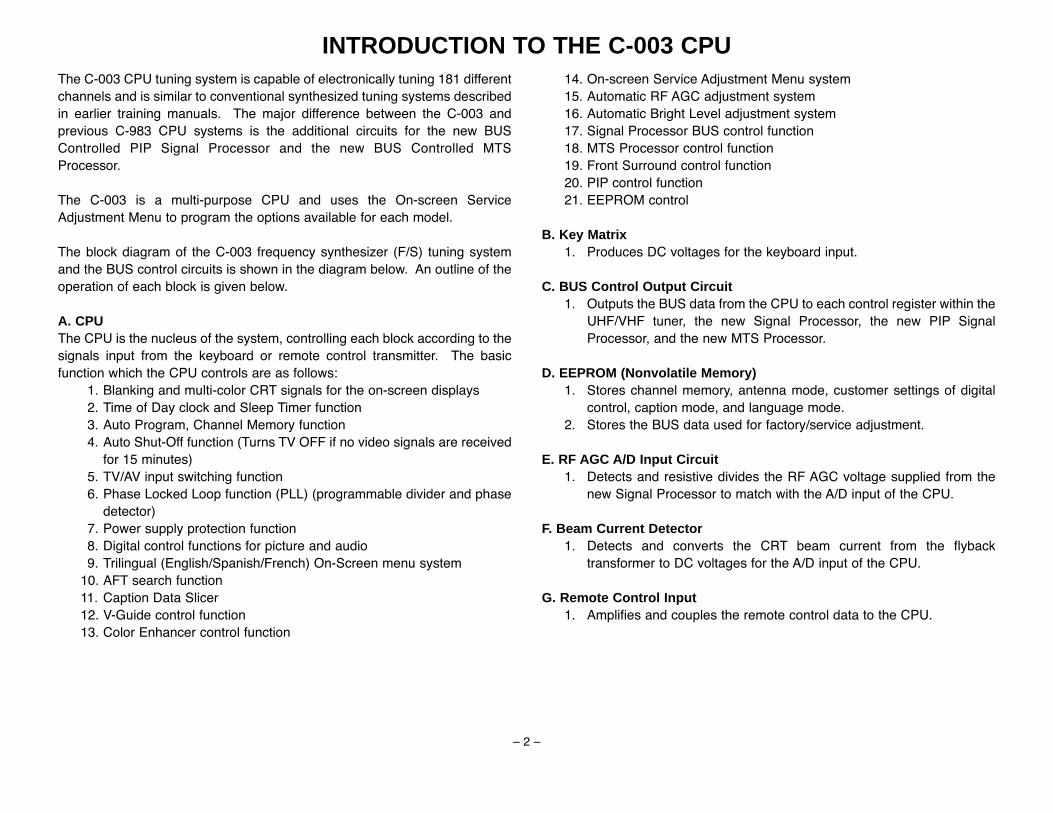
INTRODUCTION TO THE C-003 CPUThe C-003 CPU tuning system is capable of electronically tuning 181 differentchannels and is similar to conventional synthesized tuning systems describedin earlier training manuals. The major difference between the C-003 andprevious C-983 CPU systems is the additional circuits for the new BUSControlled PIP Signal Processor and the new BUS Controlled MTSProcessor.
The C-003 is a multi-purpose CPU and uses the On-screen ServiceAdjustment Menu to program the options available for each model.
The block diagram of the C-003 frequency synthesizer (F/S) tuning systemand the BUS control circuits is shown in the diagram below. An outline of theoperation of each block is given below.
A. CPUThe CPU is the nucleus of the system, controlling each block according to thesignals input from the keyboard or remote control transmitter. The basicfunction which the CPU controls are as follows:
1. Blanking and multi-color CRT signals for the on-screen displays2. Time of Day clock and Sleep Timer function3. Auto Program, Channel Memory function4. Auto Shut-Off function (Turns TV OFF if no video signals are received
for 15 minutes)5. TV/AV input switching function6. Phase Locked Loop function (PLL) (programmable divider and phase
detector)7. Power supply protection function8. Digital control functions for picture and audio9. Trilingual (English/Spanish/French) On-Screen menu system
10. AFT search function11. Caption Data Slicer12. V-Guide control function13. Color Enhancer control function
14. On-screen Service Adjustment Menu system15. Automatic RF AGC adjustment system16. Automatic Bright Level adjustment system17. Signal Processor BUS control function18. MTS Processor control function19. Front Surround control function20. PIP control function21. EEPROM control
B. Key Matrix1. Produces DC voltages for the keyboard input.
C. BUS Control Output Circuit1. Outputs the BUS data from the CPU to each control register within the
UHF/VHF tuner, the new Signal Processor, the new PIP SignalProcessor, and the new MTS Processor.
D. EEPROM (Nonvolatile Memory)1. Stores channel memory, antenna mode, customer settings of digital
control, caption mode, and language mode.2. Stores the BUS data used for factory/service adjustment.
E. RF AGC A/D Input Circuit1. Detects and resistive divides the RF AGC voltage supplied from the
new Signal Processor to match with the A/D input of the CPU.
F. Beam Current Detector1. Detects and converts the CRT beam current from the flyback
transformer to DC voltages for the A/D input of the CPU.
G. Remote Control Input1. Amplifies and couples the remote control data to the CPU.

3
C-003 Tuning System Block Diagram
TUNEREEPROM
KEYBOARD
RCPRE-AMP
DISPLAY
DIGICONSOUNDAVMTSPIPAFT
CAPTIONDATA SLICER OSD
CPU(C-003)
COMPOSITEVIDEO
RF AGCA/D INPUT
BUS CONTROLLEDSIGNAL PROCESSOR
BEAM CURRENTDETECTOR
PLLPRE-SCALER
BAND SW

4
CPU PROGRAMMINGThe On-screen Service Adjustment Menu system employed in the VB7Cchassis replaces the resistors used to change the voltage on the option pinsof the previous CPU. In order to program the CPU for the different optionsavailable for the VB7C chassis, the On-screen Service Adjustment Menu isused to change the option data in IC802, the EEPROM.
The Service Adjustment Menu display shown below and the following tableshow the different options available and the necessary data. The option datashown are for Mode AVM-2780G and include these options: with Clock, withSurround, with Software for PIP Rating Information Processing, with ColorEnhancer, with Initial Channel, with PIP, with 2 AV Inputs, and with Bass &Treble controls.
Memory Control Circuits
33
31
IC802EEPROM
6
5
R807
R808
SCL
SDA
L801
IICSCL
C801
ALWAYS 5V
IC801CPU
IICSDA

5
PROGRAM CODESThe microprocessor used in the VB7C chassis is a multi-purpose type and isused in several different models. To ensure proper operation and the correctfeatures for your particular model, the Program Codes must be correct.
Note: To enter the service adjustment menu, connect the AC power cordwhile pressing the MENU key. The service adjustment can be madewith the remote control. To exit the service adjustment mode, press theMENU key again. Refer to the specific Service Manual for your modelfor complete adjustment procedure. * . . . .When the Initial Channel option is used, the Initial Channel (the TV can
be set automatically to tune to a specific channel each time it is turnedon.) and XDS (Extended Data Service) features are available.
BIT FUNCTIONDATA
0 1
0 NOT USED 1 NOT USED 2 NOT USED
00: NONE3, 4 CLOCK 01: YES (AC 60 Hz)
10: YES (INT OSC)11: INHIBITED (=NONE)
5 NOT USED 6 SURROUND NONE YES
7 NOT USED
BIT FUNCTIONDATA
0 1
0 PIP RATING INFO. 1 COLOR ENHANCER NONE YES
2 INITIAL CHANNEL NONE YES *
3 NOT USED 4 PIP NONE YES
5 AV1 / AV1, AV2 AV1 AV1, AV2
6 TONE / BASS, TREBLE BASS, TRE. TONE
7 NOT USED
NO. DATAXXX OPT XXX XXXXXXXX
DECIMAL DATA (ZERO SUPPRESSED)
NO. 29, 30
TITLE OPT, OP2
BINARY DATA (8 bit)
Option Data 1
Option Data 2

6
Key ScanThe Key Scan circuit uses an analog circuit to generate and send voltage tothe CPU when a key is pressed. The CPU uses this voltage to determinewhich key was pressed. This resistive circuit eliminates the need forencoder/decoder devices, simplifying design and adding to the reliability ofthe receiver.
The CPU performs a key scan approximately every 20ms to check for apressed key. When the key data change is the same for two consecutivereads, it is determined that a key has been pressed and the correspondingcommand executed.
The table below shows the voltages input to CPU pin 9 when a given key ispressed.
Key InputThe function of the keys on keyboard and those of the remote controltransmitter are the same.
The following keys, when activated, perform a series step action. The time ofeach series step action is also shown below.
A . CH Up/Down 500 ms/step.B . Vol Up/Down 140ms/step. It takes about 9 seconds to change from
minimum to maximum volume.
Preceding and succeeding mutes are performed when turning power Off/On,changing channels, switching Antenna mode, searching channels, changingMTS or TV/AV mode, exchanging programs between the main screen andPIP window, or switching Surround sound mode.
Channel and Mode Change Mutes
MUTE SIGNAL MUTE OFFMUTE ON
PRECEDINGMUTE
SUCCEEDINGMUTE
MODE CHANGEPRESSING KEY
MODE OUTPUT
Key Scan Voltages
KEY INPUT VOLTAGE FUNCTION
SW1901 4.26 ~ 5.00 POWER
SW1902 3.63 ~ 4.26 VOL +
SW1903 3.01 ~ 3.63 VOL -
SW1904 2.38 ~ 3.01 CH
SW1905 1.60 ~ 2.38 CH
SW1906 1.13 ~ 1.60 MENU
OFF 0.00 ~ 1.13 –––
KEY SCAN CIRCUIT

7
9
ALWAYS5V
SW1901(POWER)
SW1902(VOL + )
SW1903(VOL )
SW1904(CH )
SW1906(MENU)
R1907R1906R1905R1904R1903R1902
R1901
C1902
L1901
R1910
IC801CPU
SW1905(CH ) D1901
(7.5V)
Key Scan Circuit
8
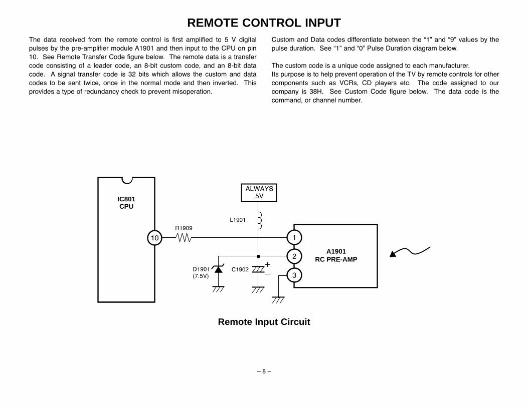
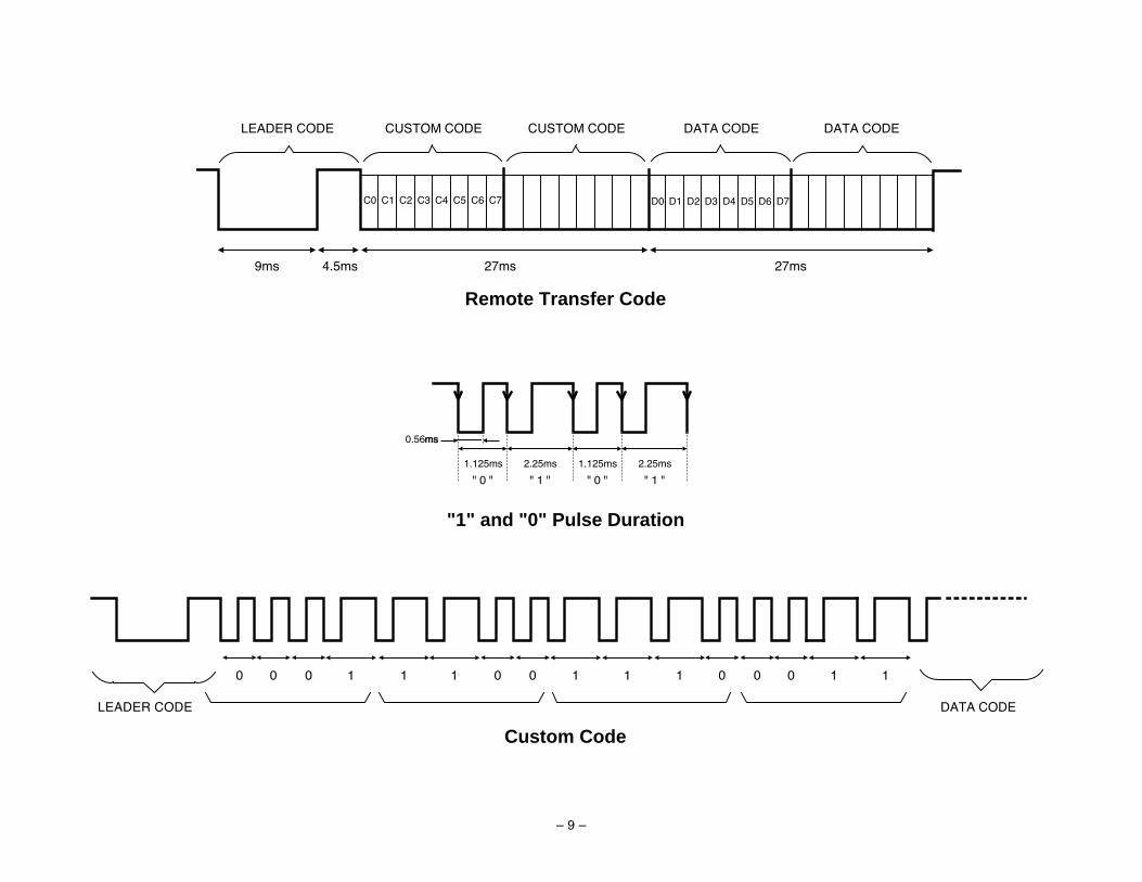
REMOTE CONTROL INPUTThe data received from the remote control is first amplified to 5 V digitalpulses by the pre-amplifier module A1901 and then input to the CPU on pin10. See Remote Transfer Code figure below. The remote data is a transfercode consisting of a leader code, an 8-bit custom code, and an 8-bit datacode. A signal transfer code is 32 bits which allows the custom and datacodes to be sent twice, once in the normal mode and then inverted. Thisprovides a type of redundancy check to prevent misoperation.
Custom and Data codes differentiate between the 1 and 9 values by thepulse duration. See 1 and 0 Pulse Duration diagram below.
The custom code is a unique code assigned to each manufacturer.Its purpose is to help prevent operation of the TV by remote controls for othercomponents such as VCRs, CD players etc. The code assigned to ourcompany is 38H. See Custom Code figure below. The data code is thecommand, or channel number.
ALWAYS5V
A1901RC PRE-AMP
10
IC801CPU
2
1
3
L1901
C1902
R1909
D1901(7.5V)
Remote Input Circuit
9
Remote Transfer Code
"1" and "0" Pulse Duration
Custom Code
LEADER CODE CUSTOM CODE CUSTOM CODE DATA CODE DATA CODE
27ms9ms 4.5ms 27ms
C0C1C2C3C4C5C6C7 D0D1D2D3D4D5D6D7
1.125ms 2.25ms 1.125ms 2.25ms
" 0 " " 1 " " 0 " " 1 "
0.56msms
0 1
LEADER CODE DATA CODE
10011100111000

10
PLL DATA OUT CIRCUITThe VB7C chassis uses a new BUS-Controlled UHF/VHF Tuner with a built-in Phase Locked Loop, Prescaler and Band Switch. Including these circuitsin the tuner reduced RF radiation and simplified shielding requirements andprinted wiring board layout. The primary difference between this chassis andthe previous chassis (C-983) is the exclusive PLL control lines (PLL Enable,PLL Data, PLL Clock) are unified to the common BUS control lines (BUS SDA,BUS SCL), and the BUS control program is incorporated in the CPU (C-003).
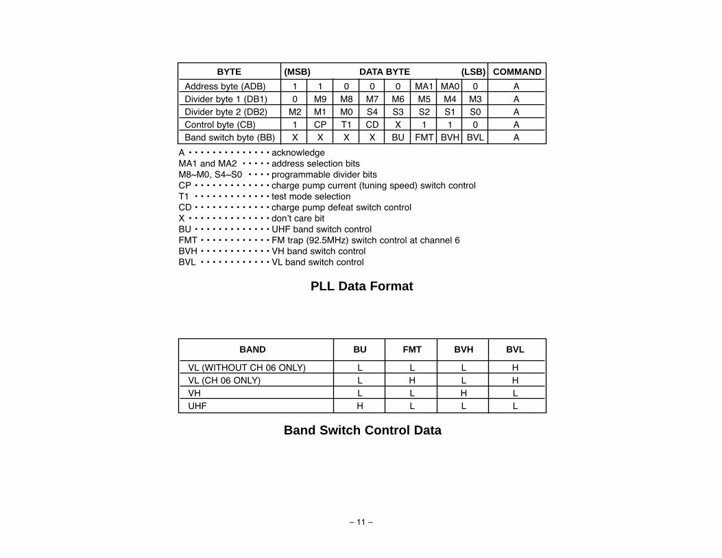
Channel selection requires only two inputs from the CPU. These are the Datasignal input from pin 32, and the Clock signal input from pin 34. The Datasignal controls the band switching, the channel selection and the AFT. Thechannel selection and the AFT function are controlled by changing the divideratio for the PLL.The tuning data format is composed of 5 byte data. See Tuning Data Formatfigure below.
PLL Data Circuit
IC801CPU
A101TUNER
DATA
CLOCK
BUSSDA
BUSSCL
32
34
R856R881
R882 R857
L881
L882
11
BYTE (MSB) DATA BYTE (LSB) COMMAND
Address byte (ADB) 1 1 0 0 0 MA1 MA0 0 ADivider byte 1 (DB1) 0 M9 M8 M7 M6 M5 M4 M3 ADivider byte 2 (DB2) M2 M1 M0 S4 S3 S2 S1 S0 AControl byte (CB) 1 CP T1 CD X 1 1 0 ABand switch byte (BB) X X X X BU FMT BVH BVL A
PLL Data Format
A acknowledgeMA1 and MA2 address selection bitsM8~M0, S4~S0 programmable divider bitsCP charge pump current (tuning speed) switch control T1 test mode selection CD charge pump defeat switch controlX dont care bitBU UHF band switch controlFMT FM trap (92.5MHz) switch control at channel 6BVH VH band switch controlBVL VL band switch control
BAND BU FMT BVH BVL
VL (WITHOUT CH 06 ONLY) L L L HVL (CH 06 ONLY) L H L HVH L L H LUHF H L L L
Band Switch Control Data

12
AFT CIRCUITThe Automatic Fine Tuning (AFT) program incorporated in the CPU functionsto fine tune the tuner local oscillator to the center of the actual broadcastfrequency. This is necessary because the transmitted TV signal may not beexactly on its assigned channel frequency. In addition, certain CATVchannels are purposely slightly offset to reduce interference from broadcastfrequencies. The operating range of the AFT is ± 2.25 MHz from FCC center.
Specifically, the AFT searches the frequency band ± 2.25 MHz from FCCcenter in 62.5 KHz steps by changing the PLL division ratios while evaluatingthe binary signals from IC101, the Signal Processor.
The station center is determined to have been found when the Time Basesignal at pin 26 is High and the AFT S-Curve signal at pin 29 is between 3.3VDC and 1.67 VDC. However, the slope (right down) is also checked todistinguish the station center from a pseudo-tuning point.
The Time Base signal is the AND signal of the horizontal sync signal from theflyback transformer and the horizontal sync signal from the video (Y) signal.
The AFT S-Curve signal is an indication of the video IF carrier frequency45.75 MHz.
The Time Base and AFT S-Curve signals are checked after each steppingaction. If station center cannot be confirmed after a complete search of theupper and lower limits of the AFT range, the frequency is returned to FCCcenter and the AFT action ceased.
The AFT only operates when first entering the channel. When entering thechannel C05 or C06, the operating range of the AFT is ± 2.25MHz from FCCcenter +125 KHz (2 steps).
AFT Circuit
IC801CPU
29 13
26
R168
7.6 V
R161
R162
AFTS-CURVE
TIMEBASE
18
C161
R376
Q371R371
R377
R372
Q372
R373
C258
R167
C371
IC101SIGNALPROCESSOR

13
RANGE OF 0 ~ 5 V
AFT S-Curve Signal
3.3 V
1.67 V
TUNINGPOINT
AFTS-CURVE
Station Center
Time Base Signal
CPUTIME BASE
SIGNAL

14
SIGNAL PROCESSOR BUS CONTROL CIRCUITThe VB7C chassis is equipped with a new single-chip BUS-Controlled NTSCSignal Processor IC to replace much of the mechanically adjustedfactory/service controls and all of the low pass filters in the PWM control linesfor the customer setting digital controls used in the conventional chassis.
The primary difference between this chassis and the conventional chassis isthe addition of the BUS Interface circuit and the movement of the controlregisters into the Signal Processor IC, and the BUS control programincorporated in the CPU (C-003).
The advantages of this chassis include reduced control lines and associatedcircuitry, and improved productivity and increased accuracy of the factoryadjustments during production. This is due to the computerized and digitizedcontrol circuit which allows remote operation.
Control of the Signal Processor IC is through CPU pins 32 and 34.
Pin 34 is the BUS SCL (Serial Data) signal. The BUS SDA is a bi-directionalsignal and is used to transfer data into and out of the control registers withinIC101. Data is processed through an 8 bit read or write for each sub addressin an IC address 1011010 with in IC101.
Signal Processor BUS Control Circuit
STA
STA = START ConditionICW = IC Address* + WriteSUB = Sub. Address*DA = Data*STO = STOP Condition
* cSee Bit Map below for IC Address,Sub Address or Data for details.
BUS Data Format In Write Mode
ICW SUB DA STO
34
32
43
44
R804
CLK
DATA
BUSSCL
BUSSDA
R803
BUSInterface
ControlRegisters
L814
L813
IC801CPU
IC101SIGNAL PROCESSOR
See Bit Map below for IC Address,Sub Address or Data for details.

15
Register Name Bits General DescriptionT Enable 1 Disable the Test SW & enable Video Mute SWVideo Mute 1 Disable video outputsSync Kill 1 Force free-run modeABL Defeat SW 1 Disable ABL functionAFC Gain 2 Select horizontal first loop gainHorizontal Phase 5 Align sync to flyback phaseIF AGC SW 1 Disable IF and RF AGCAFT Defeat 1 Disable AFT outputRF AGC Delay 6 Align RF AGC thresholdVideo SW 1 Select Video Signal (INT/EXT)PLL Tuning 7 Align IF VCO frequencyBNI Enable 1 Enable black noise inverterAudio Mute 1 Disable audio outputsAPC Det Adjust 6 Align AFT crossoverV Count Down Mode 1 Selected vertical countdown modeVertical Test Enable 3 Selected vertical DAC test modesVertical DC 6 Align Vertical DC biasVertical Kill 1 Disable vertical outputColor Kill 1 Enable Color KillerVertical Size 6 Align vertical amplitudeRed Bias 8 Align Red OUT DC levelGreen Bias 8 Align Green OUT DC levelBlue Bias 8 Align Blue OUT DC levelBlanking Defeat 1 Disable RGB output blankingRed Drive 7 Align Red OUT AC levelDrive Test 1 Enable drive DAC test modeBlue Drive 7 Align Blue OUT AC levelColor Difference Mode Enable 1 Enable Color difference modeBrightness Control 7 Customer brightness controlContrast Test 1 Enable Contrast DAC test modeContrast Control 7 Customer contrast controlTrap & Delay SW 1 Select luma filter modeAutoFlesh Enable 1 Enable autoflesh functionBlack Stretch Defeat 1 Disable black stretchSharpness Control 5 Customer sharpness controlTint Test 1 Enable tint DAC test modeTint Control 7 Customer tint controlColor Test Enable 1 Enable color DAC test modeColor Control 7 Customer color controlWhite Peak Limiter Enable 1 Disable White Peak LimiterG Drive Reduction 4 Select Green OUT AC levelV Size Compensation 3 Selected Gain of V Size CompensationVideo Level 3 Align IF video levelFM Level 5 Align WBA output levelAudio SW 1 Select Audio Signal (INT/EXT)Volume Control 7 Customer volume control
Control Register Descriptions
IC Address: BAh (10111010)Sub Address (MSB) DATA (LSB)D7 D0 DA7 DA6 DA5 DA4 DA3 DA2 DA1 DA0
$00 T_Enable Vid_Mute SSnncc KK ii ll ll(tr0) 1 0 0$01 ABL DEF AFC Gain H_Phase(tr1) 1 1 1 0 1 1 1 1$02 IF AGC SW AAFFTT DDEEFF RF_AGC_Delay (Note-1)(tr2) 0 0 1 1 0 0 1 0$03 VIDEO SW PLL TUNING(tr3) 0 1 0 0 0 0 0 0$04 N/I SW Audio_Mute APC DET ADJUST(tr4) 1 0 0 1 1 1 1 1$05 VCD MODE V_Test Ver_DC(tr5) 0 0 1 0 0 0 0 0$06 VVeerr KK ii ll ll CCoo ll KK ii ll ll Ver_size(tr6) 0 0 1 0 0 0 0 0$07 R_Bias (Note-2)(tr7) 0 0 0 0 0 0 0 0$08 G_Bias (Note-2)(tr8) 0 0 0 0 0 0 0 0$09 B_Bias (Note-2)(tr9) 0 0 0 0 0 0 0 0$0A BLK_DEF R-Drive
(tr10) 0 0 1 1 0 1 1 1$0B Drv_Test B_Drive(tr11) 0 0 1 1 0 1 1 1$0C C_Diff BBrr ii gghh tt(tr12) 0 1 0 0 0 0 0 0$0D Cot_Test CCoonn tt rraass tt(tr13) 0 1 1 1 1 1 1 1$0E Trap&D_SW A Flesh Black ST SShhaarrppnneessss
(tr14) 0 1 0 1 0 0 0 0$0F Tin_Test TTii nn tt
(tr15) 0 1 0 0 0 0 0 0$10 Col_Test CCoo lloo rr
(tr16) 0 1 0 0 0 0 0 0$11 W Peak G Drive Reduction V-Comp.
(tr17) 1 1 0 0 0 0 0 0$12 VIDEO LEVEL FM LEVEL
(tr18) 1 0 0 0 1 1 1 1$13 AUDIO SW Volume
(tr19) 1 1 1 1 1 1 1 1
The shaded data shows fixed data. The outlined data can be changed except during the Service Menu mode. The data except above can be set with the Service Menu. Note-1: shows the data that can be set with the Service Menu or the Automatic Adjustment Menu. Note-2: shows the data that can be set with the R/G/B Bias Adjustments in the Service Menu.
Bit Map

16
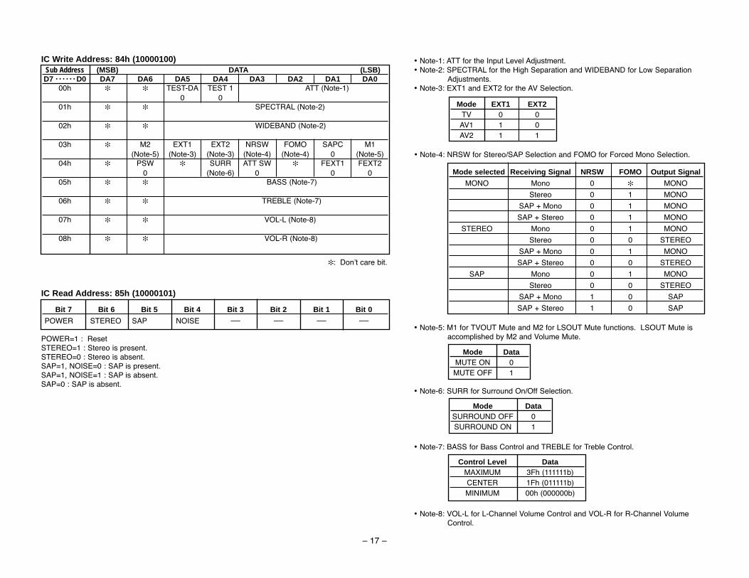
MTS PROCESSOR BUS CONTROL CIRCUITThe VB7C chassis is equipped with a new single-chip BUS-Controlled MTSProcessor IC to replace much of the mechanically adjusted factory/servicecontrols and all of the low pass filters in the PWM control lines for thecustomer setting digital controls used in the conventional chassis. In addition,the Bass, Treble and Volume control circuits have been also integrated into asingle-chip IC.
The primary difference between this chassis and the conventional chassis isthe addition of the BUS Interface circuit and movement of the control registersinto the MTS Processor IC, and the BUS control program incorporated in theCPU (C-003).
The advantages of this chassis include reduced control lines and associatedcircuitry, and improved productivity and increased accuracy of the factoryadjustments during production. This is due to the computerized and digitizedcontrol circuit which allows remote operation.
Control of the MTS Processor IC is through CPU pins 32 and 34.
Pin 34 is the BUS SCL (Serial Clock) signal. The BUS SCL input is used toclock all data into and out of IC101.
Pin 32 is the BUS SDA (Serial Data) signal. The BUS SDA is a bi-directionalsignal and is used to transfer data into and out of the control registers withinIC3401. Data is processed through an 8-bit read or write for each subaddress in an IC address 10000100 (Read Address) or 10000101 (WriteAddress) within IC3401.
MTS Processor BUS Control Circuit
R881
SCL
SDA
BUSSDA
BUSSCL
R882
IC3401MTS PROCESSOR
BUSInterface
ControlRegisters
L881
L882
R3401
R3402
STA
STA = START ConditionICA = IC Address* + Read or WriteSUB = Sub. Address* (needed only in Write mode)DA = Data*STO = STOP Condition
* cSee Bit Map below for IC Address,Sub Address or Data for details.
BUS Data Format in Write Mode
ICA SUB DA STO
32
34
5
6
IC801CPU
See Bit Map below for IC Address,Sub Address or Data for details.
17
IC Write Address: 84h (10000100)Sub Address (MSB) DATA (LSB)D7 D0 DA7 DA6 DA5 DA4 DA3 DA2 DA1 DA0
00h TEST-DA TEST 1 ATT (Note-1)0 0
01h SPECTRAL (Note-2)
02h WIDEBAND (Note-2)
03h M2 EXT1 EXT2 NRSW FOMO SAPC M1(Note-5) (Note-3) (Note-3) (Note-4) (Note-4) 0 (Note-5)
04h PSW SURR ATT SW FEXT1 FEXT20 (Note-6) 0 0 0
05h BASS (Note-7)
06h TREBLE (Note-7)
07h VOL-L (Note-8)
08h VOL-R (Note-8)
Note-1: ATT for the Input Level Adjustment. Note-2: SPECTRAL for the High Separation and WIDEBAND for Low Separation
Adjustments. Note-3: EXT1 and EXT2 for the AV Selection.
Note-4: NRSW for Stereo/SAP Selection and FOMO for Forced Mono Selection.
Mode EXT1 EXT2TV 0 0AV1 1 0AV2 1 1
Mode selected Receiving Signal NRSW FOMO Output Signal
MONO Mono 0 MONO
Stereo 0 1 MONO
SAP + Mono 0 1 MONO
SAP + Stereo 0 1 MONO
STEREO Mono 0 1 MONO
Stereo 0 0 STEREO
SAP + Mono 0 1 MONO
SAP + Stereo 0 0 STEREO
SAP Mono 0 1 MONO
Stereo 0 0 STEREO
SAP + Mono 1 0 SAP
SAP + Stereo 1 0 SAP
Note-5: M1 for TVOUT Mute and M2 for LSOUT Mute functions. LSOUT Mute isaccomplished by M2 and Volume Mute.
Mode DataMUTE ON 0MUTE OFF 1
Note-6: SURR for Surround On/Off Selection.
Mode DataSURROUND OFF 0SURROUND ON 1
Note-7: BASS for Bass Control and TREBLE for Treble Control.
Control Level DataMAXIMUM 3Fh (111111b)CENTER 1Fh (011111b)MINIMUM 00h (000000b)
Note-8: VOL-L for L-Channel Volume Control and VOL-R for R-Channel VolumeControl.
IC Read Address: 85h (10000101)
Bit 7 Bit 6 Bit 5 Bit 4 Bit 3 Bit 2 Bit 1 Bit 0
POWER STEREO SAP NOISE
: Dont care bit.
POWER=1 : ResetSTEREO=1 : Stereo is present.STEREO=0 : Stereo is absent.SAP=1, NOISE=0 : SAP is present.SAP=1, NOISE=1 : SAP is absent.SAP=0 : SAP is absent.

18
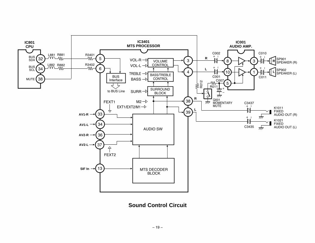
SOUND CONTROL CIRCUITThe sound level is controlled by the BUS control signal form the CPU, theBUS SDA (Serial Data) signal from pin 32, and the BUS SCL (Serial Clock)signal from pin 34. The BUS control signals from the CPU are coupled to theBUS Interface circuit within IC3401, the MTS Processor. The BUS Interfacecircuit transfers a 6-bit volume data into both of the Volume Control RegistersVOL-L and VOL-R. A 6-bit volume control data from each of the VolumeControl Registers is converted to a 0-63 steps analog signal (DC voltages) inthe Volume D/A converter for input to the Volume Control Circuit. Now theaudio signal is output from pins 3 and 4 of IC3401.
The volume control data 000000 and the audio mute control data 0 areinput to the Volume Control Registers VOL-L and VOL-R, and the Audio MuteControl Register M2 (Sub Address 03h, Bit 6), respectively to set the outputsound level to step 0/63 during Mute ON. (See page 30 for the Audio MuteControl Register M2.)In addition, the CPU outputs the Mute (High) signal from pin 38 to preventbuzz or static in the speakers when turning On/Off or during Standby mode.The Mute (High) is coupled to the base of Q001, switching Q001 On,grounding pin 5 of the Audio Amplifier IC001.
BUS Data Format in Write Mode - Volume Level at 16/63 step
STA ICW SUB DA STOSTA: START ConditionICW: IC Address + WriteSUB: Sub. AddressDA : DataSTO: STOP Condition
0 1 0 0 0 00000001 1
IC WRITE ADDRESS
1100000 1
SUB. ADDRESS
0 1 0 0 0 0
VOL-R
0000001 1 0010000 0
(LSB)(LSB) (LSB) (MSB)(MSB)(MSB)
DA0DA1DA2DA3DA4DA5DA6DA7D0D1D2D3D4D5D6D7 D0D1D2D3D4D5D6D7
DA0DA1DA2DA3DA4DA5DA6DA7D0D1D2D3D4D5D6D7 D0D1D2D3D4D5D6D7
(LSB)(LSB) (LSB) (MSB)(MSB)(MSB)
IC WRITE ADDRESS SUB. ADDRESS
VOL-LDon't care bits
Don't care bits
19
Sound Control Circuit
IC801CPU
3BUSSDA 5
64
38
R882
R881
BUSSCL
BUSInterface
SIF In
8
10
IC001AUDIO AMP.
C010L881
L882
R3401
R3402
AV1-L
AV1-R
AV2-L
AV2-R
13 MTS DECODERBLOCK
AUDIO SW
39
C002
L
R
C001
3
1C011
SP901SPEAKER (R)
SP902SPEAKER (L)
C3437
L
R
C3435
R
L
K1011FIXEDAUDIO OUT (R)
K1021FIXEDAUDIO OUT (L)
to BUS Line
32
34
IC3401MTS PROCESSOR
VOLUMECONTROL
BASS/TREBLECONTROL
SURROUNDBLOCK
VOL-R
VOL-L
BASS
TREBLE
SURR
M2EXT1/EXT2/M1
33
34
36
37
FEXT1
FEXT2
MUTE 385
C007
R011
Q001MOMENTARYMUTE
R01
2

20
DIGITAL CONTROL CIRCUITSDigital electronic controls replace the mechanical customer controls. Thisprovides a more precise setting of the controls as well as allowing theconvenience of remote operation. The BUS data output from the CPU foreach Control Register are essentially the same as those previously describedfor the Sound Control Circuit.
The BUS Interface circuit (see diagram below) is necessary to transfer eachcontrol data in the BUS data from the CPU into a corresponding ControlRegister in the Signal Processor IC101, and the MTS Processor IC3401.
After accessing the on-screen main menu system with the MENU key andselecting the Picture/Sound Manual adjustment menu with the CH / andVOL / + keys, digital control is carried out by pressing the MENU key forseven separate controls. the CH / key is used to select the control tobe changed. Each time a CH / key is pressed, the mode will advanceto the next control. The sequence is: Color, Tint, Contrast, Brightness,Sharpness, Bass and Treble. the active control will be displayed on thescreen and then can be adjusted with the VOL / + keys.
It takes 140 ms per step to change the control level with the VOL / + keys.There are 64 step control level changes in each control mode with the outputcharacteristics of each control mode independent of the others. When a VOL / + key is pressed it takes approximately 5 seconds to change from centerto minimum or center to maximum. The BUS data changes for the controlsare the same as those shown for the volume control.
When the FACTORY PRESET mode is selected with the RESET key, thePicture/Sound controls will return to the factory settings. During FACTORYPRESET mode the settings are as follows: COLOR 32/64*1, TINT 32/64*1,CONTRAST 64/64*2, BRIGHTNESS 32/64*3, SHARPNESS 32/64*4, BASS32/64, TREBLE 32/64. Furthermore, the FACTORY PRESET mode clears allthe other customized settings.
When the FACTORY PRESET mode is selected, the customized settings ofthe digital controls will be reset. If desired, customized settings can be madeagain using the on-screen menu.
*1 A 7-bit control data up to 127 steps are output for each control register.One and one half of the customer control steps (1.5x64 =96 steps) areassigned for customer setting and the remainder (31 steps) areprovided for service adjustment.
*2 A 7-bit control data up to 127 steps are output for this control register.One and one half of the customer control steps (1.5x64 =96 steps) areassigned for customer setting and the remainder (31 steps) are alwaysoutput.
*3 A 7-bit control data up to 127 steps are output for this control register.64 steps are assigned for customer setting and the remainder (63steps) are provided for service adjustment.
*4 A 5-bit control data up to 31 steps are output for this control register.One fourth of the customer control steps (1/4x64=16 steps) areassigned for customer setting and the remainder (15 steps) areprovided for service adjustment.

21
Output Range of BUS Data
IC101SIGNAL PROCESSOR
Digital Controls
32BUSSDA 44
43R804
R803L813
34BUSSCL
L814
ColorWrite7 bit
to BUS Line
Tint
Brightness
Contrast
Sharpness
BUSInterface
CRT
Vid
eo/C
hrom
aP
roce
ssin
g C
ircui
t
IC3401MTS PROCESSOR
5
6R3402
R3401
L881
L882
Volume-L/R
to BUS Line
Bass
Treble
BUSInterface
MT
S S
igna
lP
roce
ssin
g C
ircui
tR881
R882
3
4
R-OUT
L-OUT
IC801CPU
Write5 bit
Write7 bit
Write7 bit
Write7 bit
Write6/6 bit
Write6 bit
Write6 bit
FUNCTION BTSOUTPUT
RANGE OFBUS DATA
RANGE OF STEPS
CUSTOMERCONTROL
SERVICEADJUSTMENT
Color 7 0 ~ 127(0~64)/127x1.5=0/127~96/127
(0~31)/127=0/127~31/127
Tint 7 0 ~ 127(0~64)/127x1.5=0/127~96/127
(0~31)/127=0/127~31/127
Contrast 7 31 ~ 127(0~64)/127x1.5+31/127
=31/127~127/127(0)/127=0/127
Brightness 7 0 ~ 127(0~64)/127
=0/127~64/127(0~63)/127
=0/127~63/127
Sharpness 5 0 ~ 31(0~64)/31x1/4=0/31~16/31
(0~15)/31=0/31~15/31
Volume 6 0 ~ 63 0/63~63/63
Bass 6 10 ~ 54 10/63~54/63
Treble 6 10 ~ 54 10/63~54/63

22
POWER ON/OFF and PROTECTION CIRCUITSPower On/OffThe CPU performs the On/Off function through pin 27. In the Power On modepin 27 changes from Low to High, forward biasing Q681. When Q681switches On, the base of Q627 will become Low, forward biasing Q627.When Q627 (+12V Sw.) switches On, forward bias will be applied to Q486(+9V Reg.). When Q627 switches On, current will flow through relay RL601,closing the contacts and applying AC power to the degaussing circuit.
In the Power Off mode, pin 27 of the CPU will become Low. Q681 will nowbe switched Off, switching Off Q627. Then Q486 (+9V Reg.) will switch Off.With Q627 Off, current will cease to flow through RL601, opening thecontacts.
Power Supply ProtectionThe C-003 CPU provides a power source protection function to automaticallyswitch Off the power if an abnormal condition occurs in the chassis powersupplies to help prevent secondary damage.
Detection of an abnormal condition is accomplished by monitoring the +4.8V(IC301 VDD), +7.6V and the +9V DC supplies at pin 3 of the CPU.
Pin 3 is normally High, approximately 5V (Vcc). If, while the power is On, pin3 becomes Low (0.4 VCC or less) for a continuous period of approximately 1.5seconds, pin 27 (power) of the CPU will be switched Low, shutting Off thepower.
If, while the power is Off, the power is switched On and pin 3 remains Low fora period of approximately 3.0 seconds, pin 27 will be switched Low, shuttingOff the power.
In circuit operation, if all +4.8V, +7.6V and +9V supplies are their normalpotential, the diodes D312, D801, and D489 will be reversed biased. With alldiodes Off, a High of 5V will be input to pin 3 of the CPU. Should either +4.8V,+7.6V, or +9V supply become 2V or less, one of the diodes will switch On,forcing a Low at pin 3 of the CPU. The input to pin 3 is evaluated every 20ms.
Note: The C-003 CPU provides a Power Surge Protection feature. If powerfailures occur three times within 15 minutes, the CPU will automaticallystop functioning to help prevent secondary damage. (TV will not turnOn by pressing the POWER key.) To reset the operating programswithin the CPU, disconnect the AC power cord for at least 10 seconds.
Auto Shut Off FunctionThe Auto Shut Off feature operates to switch the TV Off if no video signal isreceived for a certain period of time. The Time Base signal is used within theCPU to determine the presence of an active channel. If pin 26 of the CPUgoes Low for a continuous period of approximately 15 minutes, the CPUprogram will determine that no active channel is present and activate the AutoShut Off feature. The Auto Shut Off has priority over the Sleep Timer function,however, it is inactive when the TV is in the AV (Video) mode.
Anode Current Leak ProtectionThe VB7C chassis provides an anode current leak protection circuit toautomatically switch Off the power to help prevent the risk of fire if anabnormal condition such as high voltage arcing occurs on the picture tubeanode or in the high voltage circuits due to accumulated dust or liquid spilledinto the TV cabinet.
Detection of an abnormal condition is accomplished by monitoring the Heatervoltage supply at pin 3 of the CPU. Since the high voltage arcing on thepicture tube anode or in the high voltage circuits causes excessive currentflows and lower voltage supplies from the secondary windings of the FlybackTransformer (T402), the excessive current flows are effectively monitored.
In circuit operation, the normal potential Heater voltage, approximately22VDC higher than the zener voltage (15V) of D428, is applied to the cathodeof D428, diode D429 will be reversed biased.With D429 Off, a High of 5V will be input to pin 3 of the CPU. Should thecathode voltage of D428 become 15.2V or less, D429 will, switch On, forcinga Low at pin 3 of the CPU.

23
Power and Protection Circuits
Q681
27
3
26TIME BASE
R852
AC IN
T402 (F.B.T)
CRT HEATER
ALWAYS+5V
C683R683
TIMEBASE
POWERON/OFF
POWERFAIL
R629
D629(20V)
D680
R628R627
R691Q627B4
+12V L623 D624T601 (POWER)
D683
TJ2
RL601
PS601POSISTOR
L901DEGAUSSINGCOIL
R835
+7.6VD801
TJ7 R498C497C258
D493(7.5V)
R310+4.8V
TJ5 Q486
+9VR486
R487
D486(10V)
D312
R311
D311(5V)
D489
C484D429
R428 D428(15V)
D482
R482 R497
(7V)
IC801CPU C629
C626
R489
IC681+5V REG
24
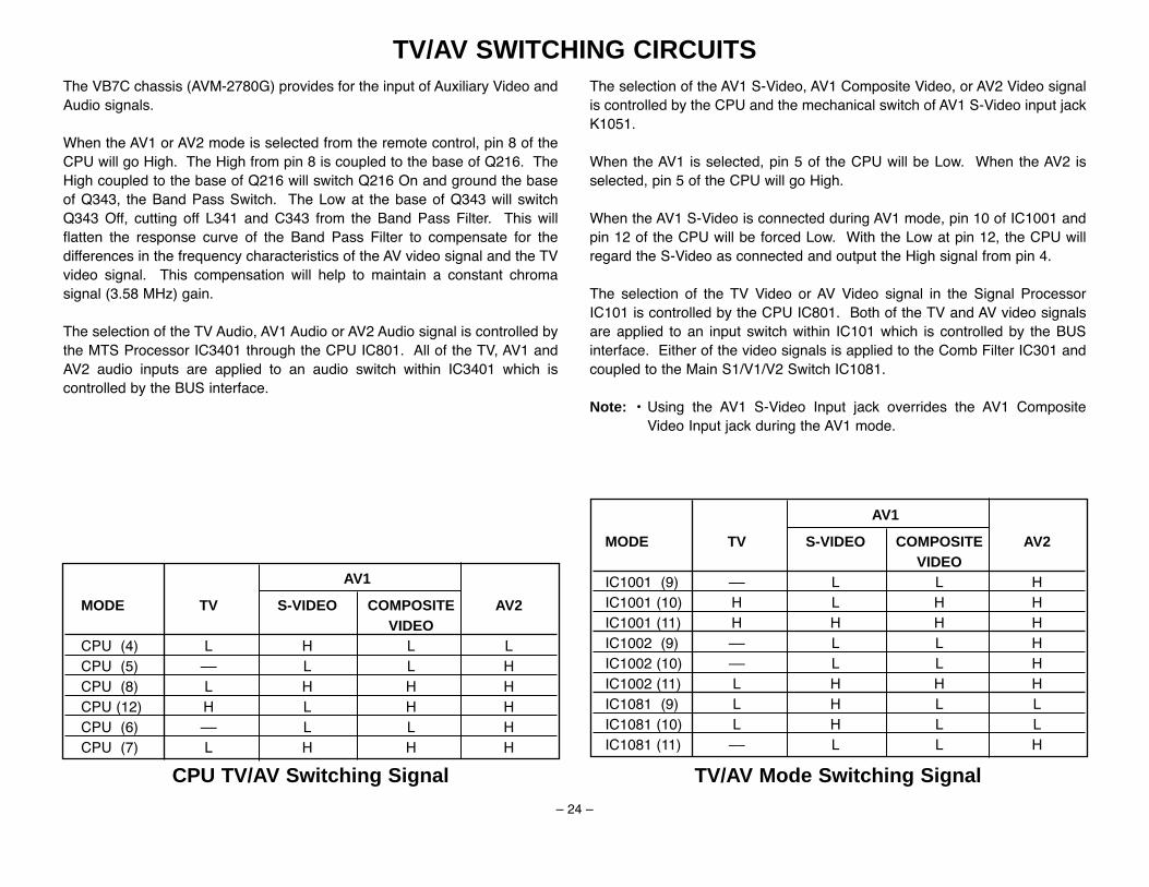
TV/AV SWITCHING CIRCUITSThe VB7C chassis (AVM-2780G) provides for the input of Auxiliary Video andAudio signals.
When the AV1 or AV2 mode is selected from the remote control, pin 8 of theCPU will go High. The High from pin 8 is coupled to the base of Q216. TheHigh coupled to the base of Q216 will switch Q216 On and ground the baseof Q343, the Band Pass Switch. The Low at the base of Q343 will switchQ343 Off, cutting off L341 and C343 from the Band Pass Filter. This willflatten the response curve of the Band Pass Filter to compensate for thedifferences in the frequency characteristics of the AV video signal and the TVvideo signal. This compensation will help to maintain a constant chromasignal (3.58 MHz) gain.
The selection of the TV Audio, AV1 Audio or AV2 Audio signal is controlled bythe MTS Processor IC3401 through the CPU IC801. All of the TV, AV1 andAV2 audio inputs are applied to an audio switch within IC3401 which iscontrolled by the BUS interface.
CPU TV/AV Switching Signal
The selection of the AV1 S-Video, AV1 Composite Video, or AV2 Video signalis controlled by the CPU and the mechanical switch of AV1 S-Video input jackK1051.
When the AV1 is selected, pin 5 of the CPU will be Low. When the AV2 isselected, pin 5 of the CPU will go High.
When the AV1 S-Video is connected during AV1 mode, pin 10 of IC1001 andpin 12 of the CPU will be forced Low. With the Low at pin 12, the CPU willregard the S-Video as connected and output the High signal from pin 4.
The selection of the TV Video or AV Video signal in the Signal ProcessorIC101 is controlled by the CPU IC801. Both of the TV and AV video signalsare applied to an input switch within IC101 which is controlled by the BUSinterface. Either of the video signals is applied to the Comb Filter IC301 andcoupled to the Main S1/V1/V2 Switch IC1081.
Note: Using the AV1 S-Video Input jack overrides the AV1 CompositeVideo Input jack during the AV1 mode.
TV/AV Mode Switching Signal
AV1
MODE TV S-VIDEO COMPOSITE AV2VIDEO
CPU (4) L H L LCPU (5) L L HCPU (8) L H H HCPU (12) H L H HCPU (6) L L HCPU (7) L H H H
AV1
MODE TV S-VIDEO COMPOSITE AV2VIDEO
IC1001 (9) L L HIC1001 (10) H L H HIC1001 (11) H H H HIC1002 (9) L L HIC1002 (10) L L HIC1002 (11) L H H HIC1081 (9) L H L LIC1081 (10) L H L LIC1081 (11) L L H

25
TV ANT
Q1621STVIDEO
11
4538
40
Q8065BUFFER
K1011FIXED AUDIO OUT (R)
TV COMP.AUDIO (L)
C
Y
Y
C
IC301COMBFILTER
K1051S1 IN
LPF
K1021FIXED AUDIO OUT (L)
5
3
1
(R)SP901SPEAKER (R)
(L)SP902SPEAKER (L)
8
10
25
24
13
47
PIPPROCESSOR
YC SEP
PIPSWITCH
Y OUT
PIP CVBS IN
SDA
SCL
Q343BANDPASSSW
VIDEODET.
K1002V2 IN
10
47
1 42
44
43
Q202BUFFER
Q306BUFFER
INPUTFILTER
Q307BUFFER
415
13
Q1071BUFFER
BAND PASSFILTER
Q342BUFFER
Q341BUFFER
Q216INVERT.
BUSInterface
BUSInterface
49MAIN Y
51MAIN C
45C OUT
Q001MOMENTARYMUTE ON/OFF
R
L
L
R
IC101SIGNAL PROCESSOR
AV1 AUDIO(L)
AV2 AUDIO(L)
AV1 AUDIO(R)
AV2 AUDIO(R)
IC001AUDIO AMP.
IC8001PIP SIGNAL PROCESSOR
34
36
37
33
IC3401MTS PROCESSOR
5
6
38
39
3
4
13
23ACK
Q8097BUFFER
Q8093BUFFER
Q8090BUFFER
Q8076BUFFER
SDA
SCL
INPUTFILTER
Q8073BUFF.
BUS SCL34
MUTE38
TV/AV8
BUS SDA32
IC801CPU
S1-SW 12
MAIN AV1/AV2 5
PIP TV/AV 7
PIP AV1/AV2 6
MAIN S SELECT 4
A101TUNER
+9V
16 15 14 13 12 11 10 9
1 2 3 4 5 6 7 8
H L H L
H L
IC1001S1/V1/V2SWITCH
R1027
+9V
16 15 14 13 12 11 10 9
1 2 3 4 5 6 7 8
H L H L
H LIC1002
PIP COMPO.
VIDEOSWITCH
R1041
+9V
16 15 14 13 12 11 10 9
1 2 3 4 5 6 7 8
H L H L
H LIC1081
MAINS1/V1/V2SWITCH
R1082
K1001V1 IN
Q1093,Q1094,Q1096
R1007
C1C1Y1
V1
R1042
C
C
Y
R1081
C1
C(COMB)
EXT.VY Y(COMB)
Q332BUFFER
YC MIX
V2
EXT V IN
INT V FOR PIP
TV/AV Switching Circuit
26
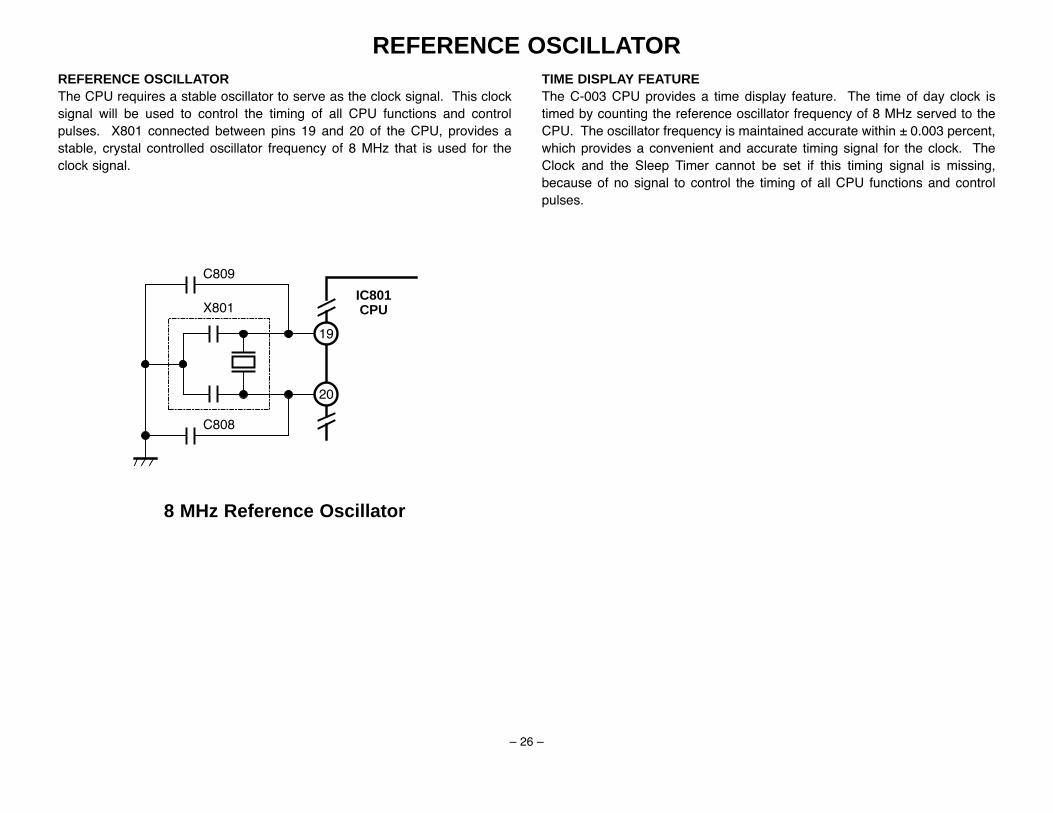
REFERENCE OSCILLATORREFERENCE OSCILLATORThe CPU requires a stable oscillator to serve as the clock signal. This clocksignal will be used to control the timing of all CPU functions and controlpulses. X801 connected between pins 19 and 20 of the CPU, provides astable, crystal controlled oscillator frequency of 8 MHz that is used for theclock signal.
TIME DISPLAY FEATUREThe C-003 CPU provides a time display feature. The time of day clock istimed by counting the reference oscillator frequency of 8 MHz served to theCPU. The oscillator frequency is maintained accurate within ± 0.003 percent,which provides a convenient and accurate timing signal for the clock. TheClock and the Sleep Timer cannot be set if this timing signal is missing,because of no signal to control the timing of all CPU functions and controlpulses.
8 MHz Reference Oscillator
IC801CPUX801
19
20
C809
C808

27
CRT DISPLAY CIRCUITThe CPU generates and controls all characters and data for the on-screendisplays. Excluding Captions, the VB7C chassis is designed for a green, red,white, yellow and cyan screen display. In order to provide correct positioning,vertical and horizontal sync signals are input to IC801 (CPU) on pins 1 (H-sync) and 2 (V-sync). The horizontal and vertical sync pulses are limited andwave shaped by Q882 and Q881 respectively.
OperationBeginning with the input of the vertical sync signal, horizontal sync pulses arecounted. After counting a certain number of horizontal sync pulses, the CPUwill begin counting 8 MHz clock pulses developed at pins 19 and 20. At the
desired number of clock pulses, the letter signals are output on pins 40-42,and the blanking signals are output on pin 39. The letter and the blankingsignals are output as active Highs. The exact count of horizontal sync pulsesand 8 MHz clock pulses is controlled by the CPU program and will changewith the display pattern.
All display signals from the CPU are input to IC101, the Signal Processor, onpins 33-36 where they are added to the video signal. Since the C-003 CPUincludes the Caption Data Slicer and Caption OSD, the screen displays andcaption displays cannot be shown simultaneously.
IC801CPU
20
19
33
34
35
5
7
X801
Q881C832 R828
IC501
T402C831
R822
Q882
R842
R846
R847
R848
R843
R844
R849
42R-OUT
41G-OUT
40B-OUT
39BLK-OUT
1H-SYNC
2V-SYNC
R827
IC101SIGNAL PROCESSOR
36
C843
C842
C841
R823
(8 MHz)
C809
C808
X-IN
X-OUT
ALWAYS5V
R821
R826
Screen Display Control Circuit

28
MEMORY CONTROL CIRCUITThe VB7C chassis is equipped with a nonvolatile memory IC to store certaininformation that should remain intact through a power failure. IC802 is the 2Kbit serial EEPROM used to store this information. An EEPROM or E2PROMis an Electrical Erasable Programmable Read Only Memory integrated circuit.
IC802 will store Channel Memory, including active and inactive channels fortotal of 125 channels, the Air/Cable mode, the customer settings of DigitalControl, Caption mode, Language mode, TV/AV mode, Surround On/Offmode, Color Enhancer mode, the Line-SW On/Off mode, and the BUS dataused for factory/service adjustments. (The Line-SW On/Off mode is a specialmode used only for production.)
Control of the memory IC is through CPU pins 31 and 33.
Pin 33 is the IIC SCL (Serial Clock) signal. The IIC SCL input is used to clockall data into and out of IC802.
Pin 31 is the IIC SDA (Serial Data) signal. The IIC SDA is a bidirectionalsignal and is used to transfer data into and out of memory. Data is processedthrough an 8 bit read or write for each address and there are 256 addresses.Therefore, IC802 has a capacity of 256 x 8 or 2K bits of data.
Memory Control Circuit
33
31
6
5
ALWAYS5V
R807
R808
SCL
SDA
L801
IICSCL
IICSDA
C801
IC802EEPROM
IC801CPU

29
S 1 10 0 0 00 0 0
START
DEVICE CODE
CONTROL BYTE
ACK
READ/WRITE
WORDADDRESS(n)
DATA n DATA n+1 DATA n+7STOP
P
NOTE : ACK=ACKNOWLEDGE BIT Write-In Mode
S 1 10 0 1 00 0 0
P
Read-Out Mode
CPU
CPU
CPU
CPU
ACK
ACK
ACK
ACK
CONTROL BYTEREAD/WRITE
NOTE : ACK=ACKNOWLEDGE BIT
DEVICE CODE
START
ACK
STOP
ACKDATA n DATA n+X
S 1 10 0 0 00 0 0
START
DEVICE CODE
CONTROL BYTE
ACK
READ/WRITE
WORDADDRESS(n)
ACK

30
MOMENTARY MUTE CIRCUITThe Momentary Mute circuit is provided to prevent buzz or static in thespeakers when changing channels. The momentary mute circuit operateswhen the power key is pressed, when changing channels, when switchingAntenna mode, when searching channels, when changing MTS or TV/AVmodes, when switching Surround On/Off mode, and when exchangingprograms between the main screen and PIP window. The momentary muteshould not be confused with the normal mute function performed by pressingthe MUTE key on the remote control. The momentary mute operates for aperiod of 0.2 to 1.6 seconds depending on the operation being performed.
The momentary mute is controlled by the BUS control signal and the Mutesignal from the CPU: the BUS SDA (Serial Data) signal from pin 32, the BUSSCL (Serial Clock) signal from pin 34, and the Mute signal from pin 38.
When changing channels, the CPU will output the BUS control signals and theMute signal to perform the momentary mute. The BUS control signals fromthe CPU are input to the BUS Interface circuit within IC3401, the MTSProcessor. The BUS interface circuit will write a 6-bit data 000000 into eachof the Volume Control Registers and a 1 bit data 0 into each of the AudioMute Control Registers to minimize the output level at pins 3, 4, 38 and 39 ofIC3401. In addition the Mute (High) is coupled to the base of Q001, switchingQ001 On, grounding pin 5 of IC001. The minimum output level at pins 3, 4,38 and 39 of IC3401 and the Low at pin 5 of IC001 will mute the audio outputof the Audio Amplifier IC001 and the external audio equipment, preventingbuzz or static in the speakers. Once the operation is complete, the CPU willoutput the BUS control signal and the Mute (Low) signal to restore the outputsound level, allowing the audio to return to normal.
BUS Data Format in Write Mode - Momentary Mute Operation
STA ICW SUB DA STOSTA: START ConditionICW: IC Address + WriteSUB: Sub. AddressDA : DataSTO: STOP Condition
0 0 0 0 0 00000001 1IC WRITE ADDRESS
1100000 1SUB. ADDRESS
0 0 0 0 0 0VOL-R
0000001 1 0010000 0
DA0DA1DA2DA3DA4DA5DA6DA7D0D1D2D3D4D5D6D7 D0D1D2D3D4D5D6D7
DA0DA1DA2DA3DA4DA5DA6DA7D0D1D2D3D4D5D6D7 D0D1D2D3D4D5D6D7
(LSB)(LSB) (LSB) (MSB)(MSB)(MSB)
IC WRITE ADDRESS SUB. ADDRESS
VOL-LDon't care bits
Don't care bits
(MSB) (LSB)
0000001 1
D0D1D2D3D4D5D6D7
(MSB) (LSB)
IC WRITE ADDRESS
1100000 0SUB. ADDRESS
D0D1D2D3D4D5D6D7
(LSB)
(LSB)
(MSB)
(MSB)
(MSB) (LSB)
DA0DA1DA2DA3DA4DA5DA6DA7
(MSB) (LSB)
0 0 0 0 0 0M2 EXT1
Don't care bit EXT2 NRSW FOMO SAPC M1
0

31
Sound Control Circuit
IC801CPU
3BUSSDA 5
64
38
R882
R881
BUSSCL
BUSInterface
SIF In
8
10
IC001AUDIO AMP.
C010L881
L882
R3401
R3402
AV1-L
AV1-R
AV2-L
AV2-R
13 MTS DECODERBLOCK
AUDIO SW
39
C002
L
R
C001
3
1C011
SP901SPEAKER (R)
SP902SPEAKER (L)
C3437
L
R
C3435
R
L
K1011FIXEDAUDIO OUT (R)
K1021FIXEDAUDIO OUT (L)
to BUS Line
32
34
IC3401MTS PROCESSOR
VOLUMECONTROL
BASS/TREBLECONTROL
SURROUNDBLOCK
VOL-R
VOL-L
BASS
TREBLE
SURR
M2EXT1/EXT2/M1
33
34
36
37
FEXT1
FEXT2
MUTE 385
C007
R011
Q001MOMENTARYMUTE
R01
2

32
AFT DEFEAT CIRCUITThe AFT Defeat circuit is provided to reduce interference or tweet in thevideo produced by the AFT circuitry. Since the AFT function is needed onlywhen changing channels, the AFT can be disabled at all other times.
The AFT enabling/disabling is controlled by the BUS control signal from theCPU: the BUS SDA (Serial Data) signal from pin 32, and the BUS SCL (SerialClock) signal from pin 34. Normally the CPU outputs the BUS control signalto disable the AFT circuitry. The BUS control signal from the CPU are inputto the BUS interface circuit within IC101, the Signal Processor. The BUSinterface circuit will write a 1 bit data 1 into the AFT Defeat Control Register
to turn off the AFT Amplifier, then the AFT output voltage at pin 13 of IC101will be fixed to 1/2Vcc (approx. 3.8VDC). When changing channels, the AFTenabling BUS data is input to the BUS Interface circuit to write a 1 bit data 0into the AFT Defeat Control Register, allowing the AFT circuit to operate.
An additional adjustment mode is provided for the service adjustment todisable the AFT Circuitry continuously for adjusting the APC DET and PLLTuning. When you enter the APC DET or PLL Tuning adjustment mode in theservice menu, the CPU will automatically output the BUS data to disable theAFT circuitry continuously.
BUS Data Format in Write Mode - AFT Defeat Operation
STA ICW SUB DA STOSTA: START ConditionICW: IC Address + WriteSUB: Sub. AddressDA : DataSTO: STOP Condition
AFTDEFEAT
0 1 0 1 1 0 0 1
RF AGC DELAY
0111101 0
IC WRITE ADDRESS
0100000 0
SUB. ADDRESS
(MSB)
IF AGC
DA0DA1DA2DA3DA4DA5DA6DA7D0D1D2D3D4D5D6D7 D0D1D2D3D4D5D6D7
(MSB)(LSB) (MSB)(LSB) (LSB)

33
IF System
TP113
BuzzCanceler
VCO
Write7 bit
PLL Tuning
W/NINV
B/N INV
AMP
Write3 bit
VideoLevel
- π / 4
+ π / 4
Video Det.
APC Det.
Write6 bit
APC Det.Adjust
VIF-1
VIF AMP10
11
9
IFGND
Write6 bit
Write1 bit
RFAGC
IF AGCDrive
RF AGCDelay
IF AGCSW
6
BUSInterface
to BUS Line
46
44
4334
32BUSSDA
BUSSCL
Data
Clock
IF AGCFilter
12
IC801CPU
LockDet
B/NINV
IFAGC
48
PLL Pull-in SW
N/I SW
Write1 bit
+
-
AFTDefeat
AFT
13
Write6 bit
VolumeD/A
Volume
AudioMute
Volume
8
51
AudioSW 5
3
2
LIMAMP
Write5 bit
FM Level
+
-
FMAMP 7
+
-50
3.8V
Multiplier5249
CLAMP
4547
VideoSW
1424
R167
C161R162R168
R161AFT Out
29AFT
S-Curve C142
PIF AGCFilter
C151
R151
PIF APCFilter
BUSGND
N/C(Vol. Filter)
N/C(Audio Out)
N/C(EXT Audio In)
T151VCO Tank
FM Filter
C131
FM Out
TP21
T131FM Coil
R133
C133
R207
SelectedVideo Out
C147
VIF VCC R159R163
R169
X1534.5MHzBPFX161
L164
TP16
C143
R143
X141SAW
IF In
TP132
R142
C106
RF AGCOut
TP11
IC101SIGNAL PROCESSOR
A
B B: When PLL Unlocked.A: When PLL Locked.
R164L166
C16
6
FM Trap(88.1 ~ 91.9MHz)
TP12
R138
C139
ExternalVideo In
InternalVideo Out
R16
0R
165
Q162
7.6V
7.6V
7.6V
VIF-2
VIF-3
7.6V
Write1 bit Write
1 bit
TP20

34
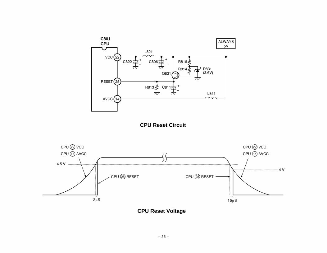
CPU RESET OPERATIONThe CPU must be reset each time AC power is applied. The reset functionensures that the 5 volt power supply is supplying sufficient power to the CPU,and the crystal-controlled reference oscillator has stabilized before the CPUmay detect inputs from the keyboard or remote control. The reset operationwill also cancel any programs operating before the power was removed. Thecircuitry to reset the CPU consists of Q831 and associated components.
After the reset function is complete, the following CPU conditions will exist:
A. Pin 27 (power) will be maintained in a Low state (TV power supplyOff).
B. The digital control functions (brightness, contrast, etc.) will be set tothe last setting modes (FACTORY PRESET or MANUAL).
C. The BUS data (sub color, sub tint, etc.) will be set to the last settings.D. The time of day clock will be reset to zero and all Timer functions
cleared.E. The volume control output is set to the last setting level.F. The channel selection will be set to last channel selected.G. The TV/AV mode will be set to the last TV/AV mode selected.H. The MTS mode will be reset to Stereo.I. The Surround mode will be set to the last Surround mode (ON or OFF)
selected.J. The PIP mode will be set to OFF.K. The Caption mode will be set to the last Caption mode selected.L. The Language mode will be set to the last Language selected.M. The Color Enhancer mode will be set to the last Color Enhancer mode
(NORMAL or WARM) selected.
The reset operation provides two functions for the CPU system First, whenpower is first applied to the system the reset circuit will initiate a microcomputer program within the CPU. This sets the CPU into the conditionsdescribed above. Second, at the time of a power failure and before the CPUcan go into disarray, the reset circuit clears any operating programs within theCPU.
When a power failure occurs, the rest program keeps the TV in the Offcondition after the power is restored, until the power key is pressed.
Reset operation – AC power applied.When AC is applied, the 5 VDC supply line to CPU pins 14 and 22 and theemitter of Q831 will gradually rise. At 2 µs after the power supply line reaches4.5 V, the collector of Q831 will change from a Low to High level. At this pointthe CPU will execute a Reset On/Off, resetting the program counter to 0(zero), and restart the program from the beginning.
Reset operation – AC power Off.When the AC power is lost, the 5 VDC supply line to CPU pins 14 and 22 andthe emitter of Q831 will gradually begin to drop. At 15 µs after the powersupply line reaches 4.5 V, the collector of Q831 will change from a High toLow level. At this point the CPU will execute a Reset Off/On, interrupt theprogram in progress, reset the program counter to 0, and enter a standbystate. When the supply line reaches 4 V, the CPU will cease to function.
35
14
IC801CPU
C811
25+
RESET
AVCC
CPU Reset Circuit
22VCC
L851
L821
ALWAYS5V
D831(3.6V)
R816
R814Q831
R813
C822+
C806+
4.5 V
2µS 15µS
CPU Reset Voltage
4 V
CPU VCC22
CPU AVCC14
CPU RESET25 CPU RESET25
CPU VCC22
CPU AVCC14

36
AUTOMATIC BRIGHT LEVEL ADJUSTMENT SYSTEMThe Automatic Bright Level Adjustment System employed in the VB7Cchassis replaces the mechanically adjusted Sub-Bright Level control used inconventional systems. The primary difference between this system andconventional systems is the addition of the beam current detection circuit andthe adjustment program incorporated within the CPU (C-003).
The advantages of this system include improved productivity and increasedaccuracy of the bright level adjustment during production. This is due to thecomputerized and digitized alignment procedure which allows remoteoperation.
A block diagram comparison of the previous and present system is shownbelow.
Note: The automatic bright level adjustment system requires specialequipment and test signals. For this reason, this system should beused only for production.An additional adjustment mode is provided in the CPU (C-003) forservice. To enter the service menu, press and hold the MENU keywhile connecting the AC power. Then select NO. 25 SB (SubBrightness) and adjust the data with the remote control. To turn off theservice menu display, press the MENU key again. Refer to the specificService Manual for your model for the complete Bright LevelAdjustment procedure.
The automatic bright level adjustment system is composed of the beamcurrent detection circuit and the automatic adjustment program in the CPU.The fundamental operations are described below.
Fundamental OperationThe BUS data for the brightness control with the 7-bit control data up to 127steps is output from IC801, the CPU. The 64 steps are used for customercontrol and the remainder (63 steps) are provided for bright level adjustment.The BUS data for the brightness control is input to IC101, the SignalProcessor, and coupled to the BUS Interface circuit within IC101. The BUSInterface circuit transfers the 7-bit control data to the Brightness ControlRegister in IC101. The 7-bit control data changes for the brightness controlare the same as those shown for the bright level on the screen.
Since the beam current required for displaying pictures on the screen issupplied from the +B (130V) DC line within the beam current detection circuit,the average beam current is detected and transformed into a DC level forinput to the CPU, pin 30 (A/D input). Maximum A/D input voltage is producedat 0 beam current.
The average beam current is in inverse proportion to the A/D input voltage asshown below. The beam current detection circuit has been designed to outputa certain DC voltage between 21/128 Vcc (0.82V) and Vcc (5.0V), at 0 beamcurrent. The CPU (C-003) has been programmed to automatically adjust thebright level at a suggested beam current for a specified video signal inputduring FACTORY PRESET mode.

37
Memory CPUD/AConverter(L.P.F)
R/CReceiver
R/CTransmitter
Tuner
SignalProcessor
Conventional Bright Level Adjustment System
Sub-Bright LevelControl
CRT
FBT
HV
DCVoltagePWM
IC802Memory
IC801CPU(C-003)
BUSInterface
A1901R/CReceiver
R/CTransmitter
A101Tuner
ContrastBright
AVM-2780G Automatic Bright Level Adjustment System
CRT
T402FBT
ABL
Beam Current Detection Circuit
+B(130V)
C829
R831
D834(18V)
D836
R833
R494
R493
R491
R492
D487
C493
HV
BrightnessControlRegister
IC101 Signal ProcessorBUSData
Special SignalInput
A/D Input Voltage
AVERAGE BEAM CURRENT ( µ A)
VccA/D Input Voltage at 0 beam current
Suggested Beam Current for12 IRE flat video signal inputduring FACTORY PRESET mode
0 100 200
5 steps (20/128 Vcc)
A/D
INP
UT
VO
LT
AG
E (
Vcc
= 5
V)
53/128 Vcc
49/128 Vcc
33/128 Vcc
29/128 Vcc
57/128 Vcc
Standard Voltage: A
Reference Voltage for specifiedbeam current during FACTORYPRESET mode
45/128 Vcc
41/128 Vcc
37/128 Vcc
D843
ALWAYS5V
38
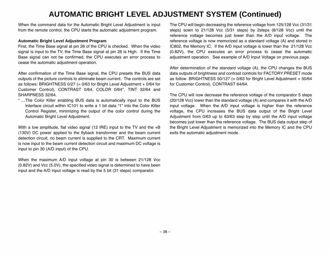
AUTOMATIC BRIGHT LEVEL ADJUSTMENT SYSTEM (Continued)When the command data for the Automatic Bright Level Adjustment is inputfrom the remote control, the CPU starts the automatic adjustment program.
Automatic Bright Level Adjustment ProgramFirst, the Time Base signal at pin 26 of the CPU is checked. When the videosignal is input to the TV, the Time Base signal at pin 26 is High. If the TimeBase signal can not be confirmed, the CPU executes an error process tocease the automatic adjustment operation.
After confirmation of the Time Base signal, the CPU presets the BUS dataoutputs of the picture controls to eliminate beam current. The controls are setas follows: BRIGHTNESS 0/27 (= 0/63 for Bright Level Adjustment + 0/64 forCustomer Control), CONTRAST 0/64, COLOR 0/64*, TINT 32/64 andSHARPNESS 32/64.* ....The Color Killer enabling BUS data is automatically input to the BUS
Interface circuit within IC101 to write a 1 bit data 1 into the Color KillerControl Register, minimizing the output of the color control during theAutomatic Bright Level Adjustment.
With a low amplitude, flat video signal (12 IRE) input to the TV and the +B(130V) DC power applied to the flyback transformer and the beam currentdetection circuit, no beam current is supplied to the CRT. Maximum currentis now input to the beam current detection circuit and maximum DC voltage isinput to pin 30 (A/D input) of the CPU.
When the maximum A/D input voltage at pin 30 is between 21/128 Vcc(0.82V) and Vcc (5.0V), the specified video signal is determined to have beeninput and the A/D input voltage is read by the 5 bit (31 steps) comparator.
The CPU will begin decreasing the reference voltage from 125/128 Vcc (31/31steps) sown to 21/128 Vcc (5/31 steps) by 2steps (8/128 Vcc) until thereference voltage becomes just lower than the A/D input voltage. Thereference voltage is now memorized as a standard voltage (A) and stored inIC802, the Memory IC. If the A/D input voltage is lower than the 21/128 Vcc(0.82V), the CPU executes an error process to cease the automaticadjustment operation. See example of A/D Input Voltage on previous page.
After determination of the standard voltage (A), the CPU changes the BUSdata outputs of brightness and contrast controls for FACTORY PRESET modeas follow: BRIGHTNESS 50/127 (= 0/63 for Bright Level Adjustment + 50/64for Customer Control), CONTRAST 64/64.
The CPU will now decrease the reference voltage of the comparator 5 steps(20/128 Vcc) lower than the standard voltage (A) and compares it with the A/Dinput voltage. When the A/D input voltage is higher than the referencevoltage, the CPU increases the BUS data output of the Bright LevelAdjustment from 0/63 up to 63/63 step by step until the A/D input voltagebecomes just lower than the reference voltage. The BUS data output step ofthe Bright Level Adjustment is memorized into the Memory IC and the CPUexits the automatic adjustment mode.

39
Automatic Bright Level Adjustment Program
Time Base signalat CPU pin 26 is High ?
Preset BUS Data Outputs to eliminate beamcurrent: BRIGHTNESS 0/127*1, CONTRAST 0/64
Read A/D Input Voltage at CPU pin 30
*1 ... 0/127 = 0/63 for Bright Level Adjustment + 0/64 for Customer Control
A/D Input Voltageis in the range*2 ?
Memorize A/D Input Voltage(Standard Voltage (A))
Change BUS Data Outputs for AUTO mode:BRIGHTNESS 50/127*3, CONTRAST 64/64
Read A/D Input Voltage at CPU pin 30
A/D Input Voltage*4< (A)-(20/128Vcc)
Increase 1 step (1/63) of BUS Data Output for Bright Level Adjustment
Memorize Bright Level
Exit Automatic Adjustment mode
(Error)
YES
NO
YES
YES
NO
NO
Enter Automatic Adjustment mode
(Error)
Wait for 100 msec
Wait for 1 sec
Wait for 200 msec
Wait for 70 msec
*2 ... range is between 21/128 Vcc (0.82V) and Vcc (5.0 V)
*3 ... 50/127 = 0/63 for Bright Level Adjustment + 50/64 for Customer Control
*4 ... A/D Input Voltage [Standard Voltage (A)] - [20/128 Vcc (0.39 V)]

40
AUTOMATIC RF AGC ADJUSTMENT SYSTEMThe Automatic RF AGC Adjustment System employed in the VB7C chassisreplaces the mechanically adjusted RF AGC control used in conventionalsystems. The primary difference between this system and conventionalsystem is the addition of the RF AGC A/D input circuit and the adjustmentprogram incorporated in the CPU (C-003).
The advantages of this system include improved productivity and increasedaccuracy of the RF AGC adjustment during production. This is due to thecomputerized and digitized adjustment procedure which allows remoteoperation.
Note: The automatic RF AGC adjustment system requires special equipmentand test signals. For this reason, this system should be used only forproduction.An additional adjustment mode is provided in the CPU (C-003) forservice. To enter the service menu, press and hold the MENU keywhile connecting the AC power. Then select NO. 03 RAD (RF AGCDelay) and adjust the data with the remote control. To turn off theservice menu display, press the MENU key again. Refer to the specificService Manual for your model for the complete RF AGC Adjustmentprocedure.
The automatic RF AGC adjustment system is composed of the RF AGC A/D(Analog/Digital) input circuit, the automatic adjustment program in the CPUand the Signal Processor. The fundamental operations are described below.
Fundamental OperationThe BUS data for the RF AGC Delay control with the 6-bit control data up to64 steps is output from IC801, the CPU. The BUS data for the RF AGCcontrol is coupled to the BUS Interface circuit within IC101 the SignalProcessor. The BUS Interface circuit transfers the 6-bit control data to the RFAGC Delay Control Register within IC101. The 6-bit control data changes forthe RF AGC Delay control are the same as those shown for the RF AGCvoltage output from pin 6 of IC101 and coupled to the AGC input terminal ofA101, the Tuner.
Since the RF AGC voltage required for the Tuner to control the AGC gain isalso connected to the RF AGC A/D input circuit, the RF AGC voltage suppliedfrom pin 6 of IC101 is detected and input to the CPU, pin 28 (RF AGC A/Dinput).
The RF AGC A/D input voltage is corresponding with the antenna input levelas shown below. The RF AGC A/D input circuit has been designed to applythe maximum rating RF AGC A/D input voltage to pin 28 of the CPU when themaximum RF AGC voltage is supplied from pin 6 of IC101. The CPU (C-003)has been programmed to automatically adjust the RF AGC voltage between69/128 Vcc (2.70V) and 85/128 Vcc (3.32V) at a specified antenna input level.

41
VideoAmp.
Tuner
Video/ChromaProcessingCircuit
Conventional RF AGC Adjustment System
RF AGCControll
CRT
DCLevel
AudioProcessingCircuit
Speaker
VideoDetector
VIFAmp.
IFAGC
RFAGC
IF VCC
SAWAGC IF
VIF/SIF Processing Circuit
ANTENNA INPUT (dB µ ) - 75 Ω / open
This curve can be moved to right or left by the RF AGC Delay Control Register.r
0 68
RF
AG
C A
/D IN
PU
T V
OL
TA
GE
(V
cc =
5V
)RF AGC A/D Input Voltage
79/128 Vcc
DOMAIN OFDISTORTION
DOMAINOF NOISE
VideoAmp.
A101Tuner
Video/ChromaProcessingCircuit
AVM-2780G Automatic RF AGC Adjustment System
CRT
DC Level
AudioProcessingCircuit
Speaker
VideoDetector
VIFAmp.
IFAGC
RF AGCAmp.
X141SAW
AGC IF
(VIF/SIF Processing Circuit)
2nd AGCFiter
IF AGCDrive
BUSInterface
Write6 bit
IC101 Signal Processor
RF AGC DelayControl Register
IC801CPU
(C-003)
A/DInput
IC802Memory
A1901R/CReceiver
R/CTransmitter
C106
BUSData
R142
R864
R862
C862
Special SignalInput
+7.6V
42
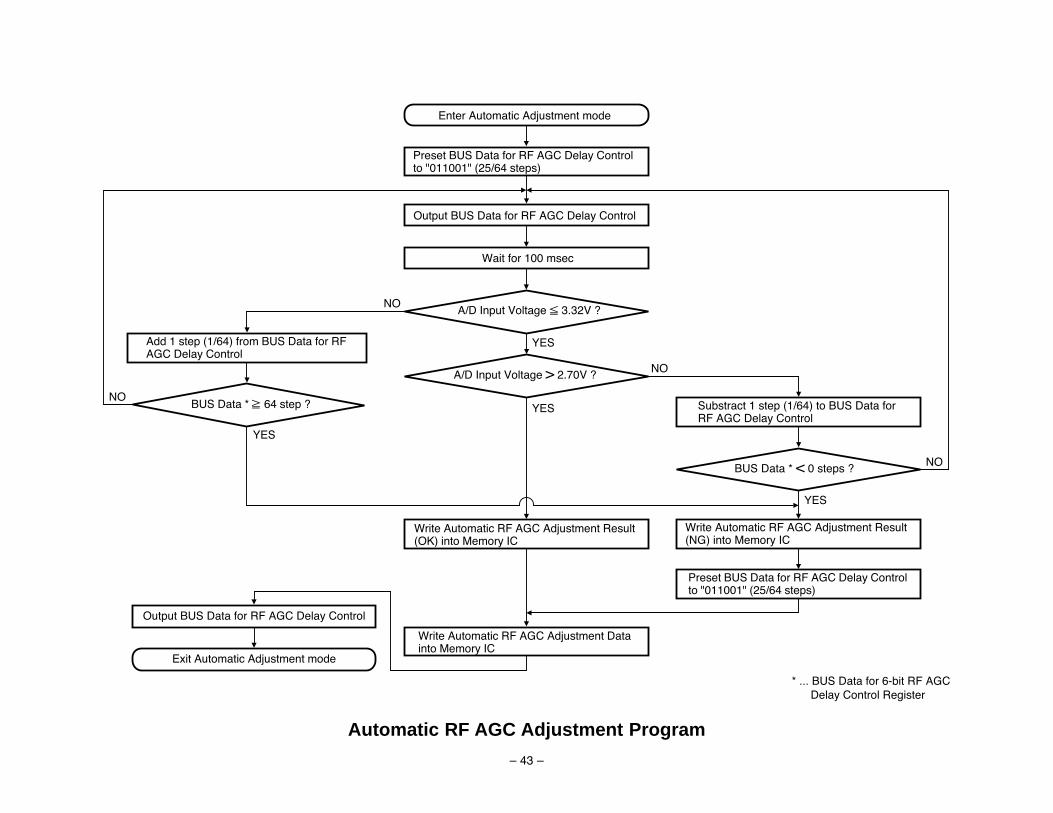
AUTOMATIC RF AGC ADJUSTMENT SYSTEM (Continued)When the command data for the Automatic RF AGC Adjustment is input fromthe remote control, the CPU starts the automatic adjustment program.
Automatic RF AGC Adjustment ProgramFirst, the CPU presets the BUS data to 011001 (25/64 steps) for the 6-bit RFAGC Delay Control Register within IC101, the Signal Processor.
With a standard field intensity (68 dBµ), specified video signal input to the TV,the RF AGC voltage (approximately 3.1V) is output from pin 6 of IC101, theSignal Processor. The RF AGC voltage will be input to pin 28 (A/D input) ofthe CPU.
At 100 msec* after the RF AGC Delay Control Register has been preset, theA/D input voltage at pin 28 of the CPU is read by the 6-bit comparator withinthe CPU.
* ....Due to the time constant of the RF AGC voltage, the CPU will wait for 100msec after the RF AGC Delay Control Register is preset before readingthe A/D input voltage so that a stable RF AGC voltage can be read.
When the A/D input voltage is between 69/128 Vcc (2.70V) and 85/128 Vcc(3.32V), the RF AGC adjustment is determined to have been normallycompleted and the BUS data in the RF AGC Delay Control Register ismemorized into IC802, the Memory IC.
If, when the A/D input voltage is read, the A/D input voltage is higher than85/128 Vcc (3.32V), the CPU will begin increasing the BUS data for the RFAGC Delay Control Register from 011001 (25/64 steps) up to 111111(64/64 steps) by 1/64 step until the A/D input voltage becomes just lower thanor equal to 85/128 Vcc (3.32V).
If, when the A/D input voltage is read, the A/D input is lower than 69/128 Vcc(2.70V), the CPU will begin decreasing BUS data for the RF AGC DelayControl Register from 011001 (25/64 steps) down to 000000 (0/64 steps)by 1/64 step until the A/D input voltage becomes just higher than 69/128 Vcc(2.70V).
When the A/D input voltage is out of the range from 69/128 Vcc (2.70V) to85/128 Vcc (3.32V) after all, the CPU will preset the BUS data for the RF AGCDelay Control Register to 011001 (25/64 steps) and store the data in IC802,the Memory IC.
43
Automatic RF AGC Adjustment Program
Enter Automatic Adjustment mode
A/D Input Voltage 3.32V ?
Preset BUS Data for RF AGC Delay Control to "011001" (25/64 steps)
Wait for 100 msec
A/D Input Voltage > 2.70V ?
YES
NO
Output BUS Data for RF AGC Delay Control
Substract 1 step (1/64) to BUS Data for RF AGC Delay Control
BUS Data * < 0 steps ?
Write Automatic RF AGC Adjustment Result (NG) into Memory IC
Write Automatic RF AGC Adjustment Result(OK) into Memory IC
Preset BUS Data for RF AGC Delay Controlto "011001" (25/64 steps)
Write Automatic RF AGC Adjustment Datainto Memory IC
Add 1 step (1/64) from BUS Data for RFAGC Delay Control
BUS Data * 64 step ?
Output BUS Data for RF AGC Delay Control
Exit Automatic Adjustment mode
* ... BUS Data for 6-bit RF AGC Delay Control Register
YES
NO
YES
NO
YES
NO

44
CLOSED-CAPTIONING DESCRIPTIONThe VB7C chassis provides for the decoding and displaying the latest Closed-Captioning information transmitted with many of todays television broadcasts.
Captioning is a printed version of the program sound or other informationdisplayed on the screen. Television stations and Cable companies controlwhich programs are broadcast with these services. At the present, there aretwo types of Closed-Captions in use, Captions and Text.
CaptionsCaptions are video related information and are normally one or two lines, butcan be up to four lines, appearing anywhere on the screen. They can bedisplayed as roll-up, pop-on, or paint-on. In the roll-up mode, captioninformation is displayed in two, three or four consecutive rows. Data appearsin the bottom row and scrolls up as new information is received. In the pop-on mode, two memories are used. One memory is displayed while the otheris receiving new data. When the proper command is received the memoriesare swapped, causing the complete caption to appear at once. In the paint-on mode, the characters are displayed as they are received, one column at atime from left to right.
TextText is non-video related information and is displayed in a black box whichoverwrites the screen. In a full screen Text mode the box is 15 rows high and34 columns wide. The rows may contain a maximum of 32 characters. Whenall 15 rows have been used, the display scrolls up as additional data isreceived.
ChannelsThe closed-caption system provides for four different data channels. The are;Captions-Language l (C1), Captions-Language ll (C 2), Text-Language l (T1),and Text-Language ll (T2). Both languages can be English, Spanish or anyother language in either case.
The complete captioning information, including location, color, characters,commands, channel etc., is transmitted using an encoded composite datasignal sent on Line 21, field one of the TV signal.
The caption data on Line 21 consists of a seven cycle sine-wave clock run-inburst, a start bit and two bytes of data. Each byte is an 8 bit alphanumericcharacter based on the USA Standard Code for Information Interchange(USASCll) with odd parity. Additional codes have been added for foreigncharacters and special symbols. The Clock rate is .5035 MHz (32 fH).

45
Line 21 Field 1 Encoded Composite Data Signal
D1 D7 D1P D7 P
H-sync ProgramColorBurst
Character 1 Character 2
Start Bit
Clock Run-in(7 Cycles)
CLOCK PULSEin BURST
Odd Field

46
THE CLOSED CAPTION DECODER SECTIONThe closed-caption decoder system used in the VB7C type chassis is capableof processing and displaying all of the latest standard line 21 closed-captiontransmissions.
The system employed in the VB7C chassis is comprised of two blocks: theData Slicer and the Screen Display Controller (OSD). Notice from the blockdiagram below that the Data Slicer and the Screen Display Controller areintegrated into the CPU. The other components necessary for displaying thecaption data are shared circuits already in use for normal TV video.
Data SlicerThe Data Slicer extracts the caption data encoded on line 21 field 1 of thecomposite video signal. The data is limited, shaped to a digital signal andoutput to the OSD block through the Internal Bus. The Data Slicer alsogenerates the clock signal, the 21H detection pulse, and the odd/even fielddiscrimination pulse required for decoding the caption data.
On Screen DisplayThe OSD block interprets the digital data signal input from the Data Slicerthrough the Internal Bus. Specifically, the Data Slicer applies error detectionand correction to the incoming data and evaluates the data for display formatand character attributes. The OSD then directs the operation of the DisplayRAM and Character ROM of the OSD. In addition, the OSD block controls themode selection (Caption/Text, C1/C2 etc.) based on the on-screen menudirectives. The OSD generates the R, G, B and blanking signals and controlsthe character type (upper/lower case, italics and color attributes) based on thecommands from the OSD Controller. Included in the OSD section is a DisplayRAM for storage and display of the recovered data and a CharacterGenerator. Serial data input from the Data Slicer is written to the Display RAMand input to the Character Generator. The Character Generator contains theCharacter ROM which holds the dot pattern for all the characters. TheCharacter Generator outputs the characters corresponding to the displaydata. The character display area is a 26 x 16 dot matrix surrounding a 18 x13 character. The additional area provides for spacing between charactersand underlining.

47
OSD Control Registers CompositeVideo signal
Closed-Caption Decoder Block Diagram
OSDRAM
OSDROM
H-Sync
V-Sync
IC801CPU(C-003)
INT
ER
NA
L B
US
Shift Register Output Circuit
OSDController
OSD Control Register (address 00D016)
Horiz. Position Register (address 00D116)
Block Control Register (address 00D216, 00D316)
Vert. Position Register (address 00D416, 00D516)
Window Register (address 00D616, 00D716)
I/O Polarity Control Register (address 00D816)
Raster Color Register (address 00D916)
B output
G output
BOX output
R outputG
R
B
OUT1
42
41
40
39
1
2
23
24OSC
N/C
Data Slicer
DATA SLICER CLOCK(27MHz)
OSC1
OSC2
17
C854
R854
R853
C853
2 bytes x 32 characters x 2 lines
16 dots x 20 dots x 254 characters
16 bit

48
CAPTION DATA SLICERThe Data Slicer extracts the caption data encoded on ling 21, field 1 (odd) ofthe composite video signal for input into the OSD Controller included in theCPU. The Data Slicer also generates the necessary clock and synchronizingsignals required for decoding the data.
Operation:CLAMP CIRCUIT, LOW PASS FILTERComposite video (2 Vp-p) is AC coupled to the CPU on pin 17 and clampedby an internal clamp circuit. The clamp circuit clamps the sync tips of thevideo to a fixed reference voltage to provide a degree of noise rejection. Fromthe clamp circuit the composite signal is coupled to the Low Pass Filter toattenuate the noise within the composite signal.
SYNC SLICERThe composite signal from the Low Pass Filter is coupled to the Sync Slicerand the composite sync signal extracted from the composite video signal.
SYNC SEPARATOR, TIMING GENERATORThe composite sync signal from the Sync Slicer is input to the Sync Separatorand separated into the horizontal sync signal (Hsep) and the vertical syncsignal (Vsep).
The Timing Signal Generator controlled by the Data Slicer Control Registers1-2 generates a reference clock signal with a clock rate of 13.0832MHz(832fH). The clock signal, the separated horizontal sync signal and theseparated vertical sync signal are used to generate other timing signalsrequired for the Data Slicer. The reference clock signal generated from theTiming Signal Generator is also used as the clock for the OSD Controller.
The horizontal sync signal (Hsep) is generated and synchronized with thehorizontal sync signal within the composite sync signal. The vertical syncsignal (Vsep) is generated at the first rising point of the timing signal and acertain period of time has past after the composite sync signal has become aLow level (see Figure below).
CompositeSync Signal
Timing Signal
Vsep Signal
Timing of Generating Vsep Signal
Vsep is generated at this rising point.
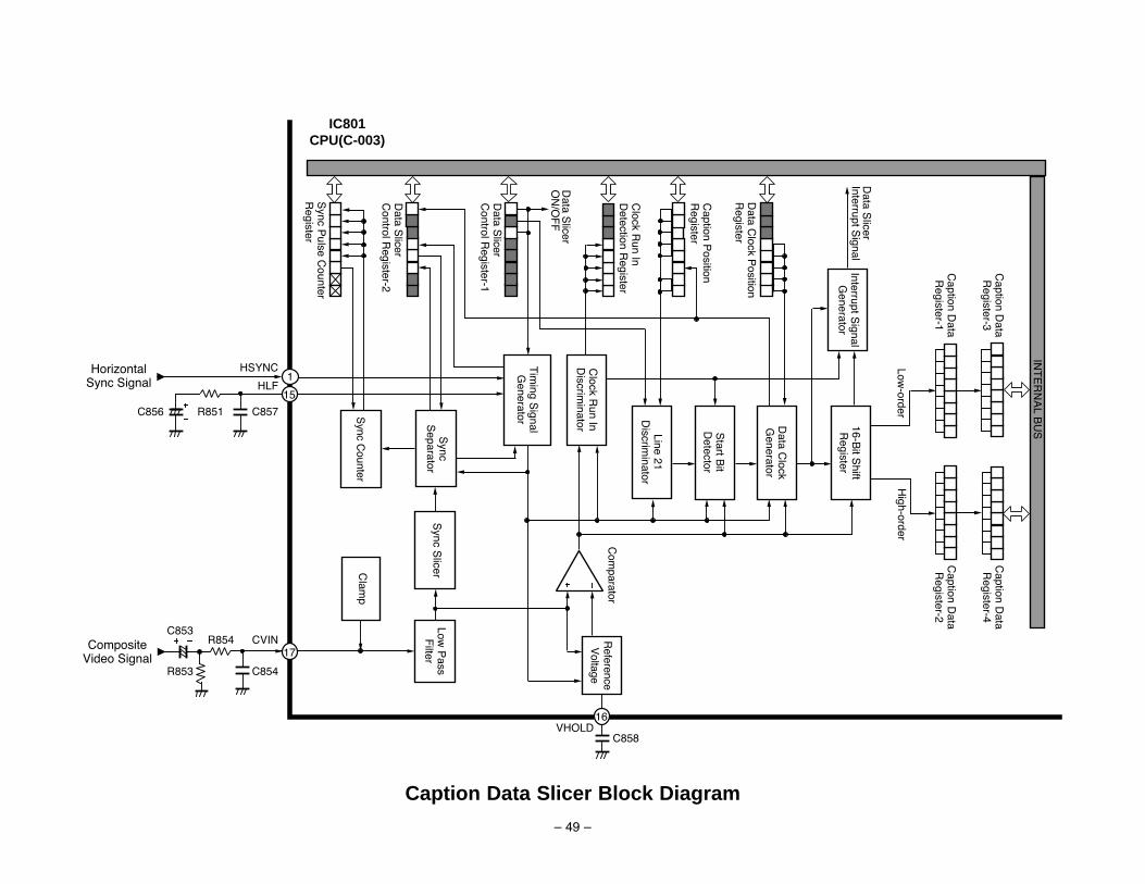
49
Caption Data Slicer Block DiagramC
lamp
Sync C
ounter
Low P
assF
ilterS
ync Slicer
Sync
Separator
Tim
ing Signal
Generator
Clock R
un InD
iscriminator Line 21
Discrim
inator
Start B
itD
etector
Data C
lockG
enerator
16-Bit S
hiftR
egister
ReferenceV
oltage
Caption D
ataR
egister-3
Interrupt Signal
Generator
Data S
licerInterrupt S
ignal
Sync P
ulse Counter
Register
Data S
licerC
ontrol Register-2
Caption P
ositionR
egister
Data C
lock Position
Register
15
1
17
16
C853
R853
R854
C854
C856 R851 C857
HLF
HSYNC
CVIN
VHOLDC858
Com
parator
IC801CPU(C-003)
Data S
licerO
N/O
FF
INT
ER
NA
L BU
S
Clock R
un InD
etection Register
Data S
licerC
ontrol Register-1
CompositeVideo Signal
HorizontalSync Signal
t
Caption D
ataR
egister-1
Caption D
ataR
egister-4
Caption D
ataR
egister-2
Low-order
High-order

50
CAPTION DATA SLICER (Continued)REFERENCE VOLTAGE GENERATOR, COMPARATORThe Reference Voltage Generator generates the reference voltagecorresponding to the amplitude of Clock Run-In Burst in line 21 field 1 of thecomposite video. Line 21 is detected by the Line 21 Discriminator. Thecomposite video signal is compared with the reference voltage and convertedinto digital pulses in the Comparator.
LINE 21 DISCRIMINATORThe Line 21 Discriminator detects line 21 in which the caption data isencoded. Line 21 discrimination is determined by counting the number ofseparated horizontal sync pulses (Hsep) between the falling point of theseparated vertical sync pulse (Vsep) and the incoming line 21 of thecomposite video signal, and then comparing the number to the data in theCaption Position Register. Field discrimination is determined by the data inthe Data Slicer Control Register-1 and 2.
START BIT DETECTORThe Start Bit Detector detects a start bit on Line 21 detected by the Line 21Discriminator.
CLOCK RUN-IN DISCRIMINATORThe Clock Run-In discrimination is accomplished by counting the number ofthe output pulses from the Comparator in the window set up after the firstpulse of the Clock-Run In.
16-BIT SHIFT REGISTERThe output signal from the Comparator is stored in the 16-Bit Shift Registeronly when the data clock is output. The caption data is obtained by readingout the higher byte (8 bits) in the caption data from the Caption Data Register2 and 4 and the lower byte in the caption data from the Caption Data Register1 and 3, after the interrupt signal has been generated.
INTERRUPT SIGNAL GENERATORThe Interrupt Signal Generator outputs the interrupt signal after the line 21assigned by the Caption Position Register has been sliced off.
SYNC COUNTERThe Sync Counter counts the number of the composite sync pulses separatedfrom the composite video signal by the Data Slicer, or the horizontal syncpulses (HSYNC) input from pin 1 of the CPU, and stores the counted data intothe Sync Pulse Counter Register.

51
Signals In Vertical Interval
Video Signal
CompositeVideo
Vsep
Hsep
Vertical IntervalCaption Data
Line 21
Caption Data (Enlarged)
Hsep
VideoSignal
Clock Run-InStart Bit + 16 Data
The presence of the Clock Run-In is determinedby the number (4 - 6) of Clock Run-In pulses in the Window.
Window
Data SlicerTiming ControlSignal

52
F/S TUNING SYSTEM DESCRIPTIONThe C-003 Frequency Synthesizer Tuning System is similar to previous PLL(Phase Locked Loop) systems described in earlier training manuals. Theprimary difference between this system and previous systems is that much ofthe system has been integrated into a single IC and included in the Tuner.
The advantages of this new synthesizer IC tuner package include: single ICchip and a smaller circuit board due to synthesizer integration, reducedcontrol lines are required from the CPU (2 versus 3), and reduced powerconsumption, RF radiation and interference.
A block diagram comparison of the previous and present system is shownbelow.
In operation, the tuner is precisely adjusted to the frequency of the channelselected by phase comparing (after frequency division) the tuner localoscillator frequency with a crystal controlled oscillator reference frequency inthe MIX-OSC/PLL IC (CXA3135AN). Any deviation of the local oscillatorfrequency from the correct channel frequency will result in an output from thephase detector.
The output from the phase detector is amplified and used to control the exactfrequency of the tuner local oscillator.
Channel selection is accomplished by control pulses from the CPU whichdetermine the frequency division ratio of the programmable divider in the MIX-OSC/PLL IC.
Previous Synthesizer Tuning Systems AVM-2780G Synthesizer Tuning System
CPU
TUNER
DATA CLOCK
CPU
TUNER
DATA CLOCK ENABLE

53
BYTE (MSB) DATA BYTE (LSB) COMMAND
Address byte (ADB) 1 1 0 0 0 MA1 MA0 0 A
Divider byte 1 (DB1) 0 M9 M8 M7 M6 M5 M4 M3 A
Divider byte 2 (DB2) M2 M1 M0 S4 S3 S2 S1 S0 A
Control byte (CB) 1 CP T1 CD X 1 1 0 A
Band switch byte (BB) X X X X BU FMT BVH BVL A
PLL Data Format
A acknowledgeMA1 and MA2 address selection bits (See Table 1)M8~M0, S4~S0 programmable divider bits: N = M8x213 + . . . + S2x22 + S1x2 + S0CP charge pump current (tuning speed) switch control T1 test mode selection CD charge pump defeat switch controlX dont care bitBU UHF band switch controlFMT FM trap (92.5MHz) switch control at channel 6 (See Table. 2)BVH VH band switch controlBVL VL band switch control
BAND BU FMT BVH BVL
VL (WITHOUT CH 06 ONLY) L L L H
VL (CH 06 ONLY) L H L H
VH L L H L
UHF H L L L
Table 2. Band Switch Byte
Table 1. Address Byte
Voltage applied to the AddressInput (ADSW) of Tuner
MA1 MA2 Address
0 to 0.5V 0 0 C0 h
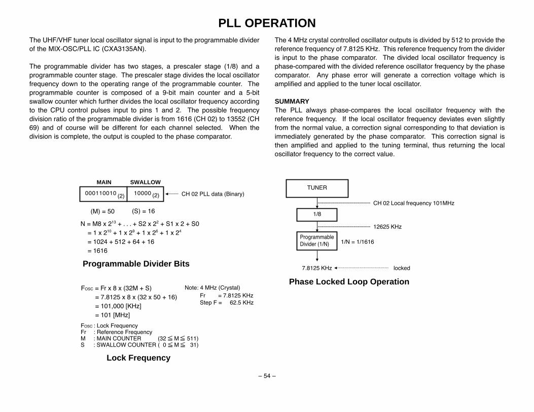
54
PLL OPERATIONThe UHF/VHF tuner local oscillator signal is input to the programmable dividerof the MIX-OSC/PLL IC (CXA3135AN).
The programmable divider has two stages, a prescaler stage (1/8) and aprogrammable counter stage. The prescaler stage divides the local oscillatorfrequency down to the operating range of the programmable counter. Theprogrammable counter is composed of a 9-bit main counter and a 5-bitswallow counter which further divides the local oscillator frequency accordingto the CPU control pulses input to pins 1 and 2. The possible frequencydivision ratio of the programmable divider is from 1616 (CH 02) to 13552 (CH69) and of course will be different for each channel selected. When thedivision is complete, the output is coupled to the phase comparator.
The 4 MHz crystal controlled oscillator outputs is divided by 512 to provide thereference frequency of 7.8125 KHz. This reference frequency from the divideris input to the phase comparator. The divided local oscillator frequency isphase-compared with the divided reference oscillator frequency by the phasecomparator. Any phase error will generate a correction voltage which isamplified and applied to the tuner local oscillator.
SUMMARYThe PLL always phase-compares the local oscillator frequency with thereference frequency. If the local oscillator frequency deviates even slightlyfrom the normal value, a correction signal corresponding to that deviation isimmediately generated by the phase comparator. This correction signal isthen amplified and applied to the tuning terminal, thus returning the localoscillator frequency to the correct value.
MAIN SWALLOW
CH 02 PLL data (Binary)000110010 10000(2) (2)
Programmable Divider Bits
Phase Locked Loop Operation
TUNER
1/8
CH 02 Local frequency 101MHz
12625 KHz
ProgrammableDivider (1/N)
7.8125 KHz
1/N = 1/1616
locked
N = M8 x 213 + . . . + S2 x 22 + S1 x 2 + S0 = 1 x 210 + 1 x 29 + 1 x 26 + 1 x 24 = 1024 + 512 + 64 + 16 = 1616
Lock Frequency
FOSC = Fr x 8 x (32M + S) = 7.8125 x 8 x (32 x 50 + 16) = 101,000 [KHz] = 101 [MHz]
(M) = 50 (S) = 16
Note: 4 MHz (Crystal)Fr = 7.8125 KHzStep F = 62.5 KHz
FOSC : Lock FrequencyFr : Reference FrequencyM : MAIN COUNTER (32 M 511)S : SWALLOW COUNTER ( 0 M 31)

55
PHASECOMPARATOR
CHARGEPUMP
BAND SW
REF. DIVIDER1/512
REF. OSD
28
29123
I2C BUSRECEIVER
18-bit SHIFTREGISTER
PRESCALER1/8
4 5 6 7
DECODER CPU
TUNERCHARGE
PUMP OUTBUBVHBVL
LOCAL
(CXA3135AN)
MAIN COUNTER SWALLOWCOUNTER9-bit 5-bit
PROGRAMMABLEDIVIDER
4-bit14-bit
ADSW SDA SCL
7.8125 KHz
4 MHz
7.8125 KHz
REF. OSC4 MHz CRYSTAL
Synthesizer Tuning Circuit
LOCKDET.
BAND SWDRIVER
UHF/VHFLOCAL OSC
BUFFER
26
LOCKFMT

56
PIP CONTROL CIRCUITThe AVM-2780G provides for Picture In Picture (PIP) function throughIC8001, the PIP Signal Processor IC.The PIP circuits perform PIP On/Off, PIP Swap, PIP Location, PIP Freeze andPIP Select functions.The PIP functions are operated using the remote control transmitter.
The PIP circuits are controlled by the PIP Signal Processor IC8001 throughthe CPU IC801. The PIP Signal Processor IC8001 requires 6 inputs: the
CPU, the horizontal and vertical sync circuits, the PIP sync separation circuitand the PIP 3.3 VDC supply circuit. There are two inputs from CPU; the SDA(Serial Data) input/output from pin 32, and the SCL (Serial Clock) input frompin 34. The Data signals control the PIP On/Off, the PIP Swap, PIP Location,PIP Freeze and PIP Select functions. When the power is switched On, the 12VDC and PIP 3.3 VDC supply lines will gradually rise. At 60ms after pin 27 ofthe CPU goes High, IC8001 will execute a Power On Reset, initializing allinternal registers to 0 (zero) and resetting the BUS interface.
60ms5V
0V
H
L
(POWER:OFF ON)
PIP Power On Reset
PIP Control Data Signals (BUS Data Transfer)
POWER ON
160ms
(POWER ON RESET)
MSB
1 2 7 8 9
MSB
1 2 7 8 9
ACKACK
StartCondition
StopConditionS IC Address Data Byte
Sub Address = auto-incrementsA = Acknowledge bitS = Start bit
P = Stop bit
0 Sub Address
n Bytes
IC Address = 24 hex (00100100)
IC8001
CPU
CPU
CPU
A A A P
(BUS SDA)
(BUS SCL)
(ACK)IC8001

57
IC801CPU
32
34
1
12V
2
17
24
25
32
33
BUSSDA
BUSSCL
H-SYNC
V-SYNC
R8004
C831
R822
Q882
Q881
R827
C832 R828
R823
C8002
L8036
R8097
MAIN PIX H-SYNC
MAIN PIX V-SYNC
5
7
T402
IC501
IC8001PIP SIGNAL PROCESSOR
PIP Control Circuits
R8006
9V
R8036
C8036
SCL
SDA
POWER ON RESET
3.3V
L8094
L8098
H-PULSE
V-PULSE
ALWAYS5V
R821
R826
L8008
Q8006
R8003
R8005
L8007
Q8005
L8036
C8003
R8095R8088
Q8097 R8096
23ACK
R8091
R8090
R8092
R8089
R8093
Q8090
Q8093
L8070
Q8000
R8002
R8001
R8009
D8000(3.9V)
C8072
3.3V
58
PIP CIRCUITSThe new YC Picture In Picture (PIP) system employed on the VB7C (AVM-2780G) is different from the previous PIP system on the VB7A chassis. Theprimary difference between this system and the previous system is that the V-chip data slicer and the Y/C processing of the sub-picture signal have beenprovided in the new PIP Signal Processor.
Since the sub-picture signal is Y/C separated and Y/C processed within thenewly developed PIP Signal Processor, the signal processing is simplified andthe picture quality is improved.
When the PIP circuits are activated by the CPU through the remote controltransmitter, the PIP circuits provide five functions to control the PIP screen.These are :
1. PIP On/Off turns the PIP screen On or Off.2. PIP Location changes the PIP screen position from corner to
corner on the screen.3. PIP Swap switches pictures between the TVs main screen
and PIP screen.4. PIP Freeze to obtain a still picture on the PIP screen.5. PIP Select to select Video 1 or Video 2 screen.
The PIP signal processing is accomplished by the TV/AV switching circuit, thePIP Signal Processor and other video circuits. The fundamental operationsare described below.
PIP Signal ProcessorThe PIP Signal Processor IC8001 is composed of the sub-picture Y/Cprocessing circuits and the Y/C Input/Output Switch. The PIP SignalProcessor contains the sub-picture signal processing circuit. The built-in fieldmemory (96K-bit RAM) is necessary to provide for the data storage of a sub-picture into the main-picture of a television.
The sub-picture processing circuit includes the A/D Converter, Y/C Separator,V-Chip Data Slicer, Timing Control, Vertical Filter, Multiplexer, Field Memory,Demultiplexer, Encoder, D/A Converters, and Y/C Input/Output Switch. Allnecessary controls are provided by registers in the PIP Signal Processor.These registers are set by external control through the BUS Interface.
One of the TV, AV1 and AV2 composite video signal is selected in the TV/AVSwitching circuits which is controlled by the BUS interface. The selectedvideo signal is applied to the sub-picture processing circuitry and input to theY/C mode switch. The Y/C mode switch selects and inserts the sub-pictureY/C signal into the main-picture Y/C signal when the PIP mode is selected.
In operation, IC8001 overlays a single sub-picture on the main video in 1/9thsize. In 1/9th the sub-picture is 228 samples (171Y, 28.5 BY, 28.5 RY) by69 lines.
The selected TV or AV video is output from the Y/C Input/Output switch (pins45 and 47 of IC8001) mixed with the PIP overlay when the PIP On mode isselected. The Y and C signals output from pins 45 and 47 of IC8001 are inputto pins 40 and 38 of the Signal Processor IC101 respectively.
Note: Using the S-Video Input jack overrides the Composite Video Inputjack when the AV1 is selected.
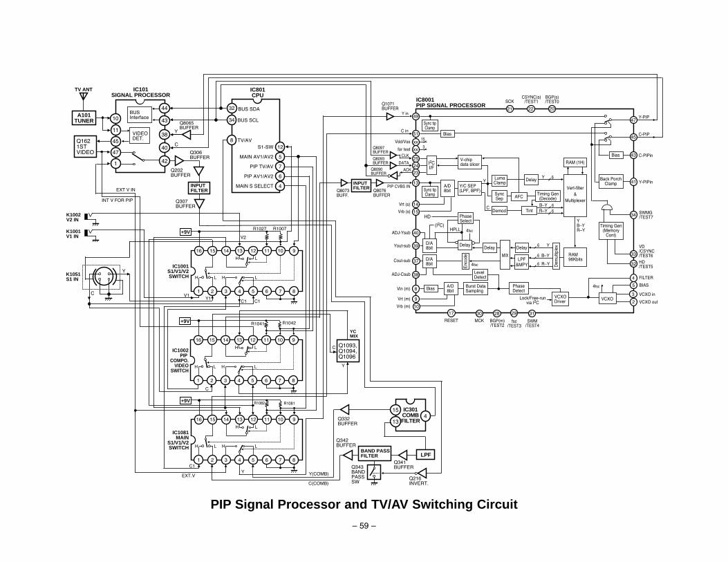
59
TV ANT
Q1621STVIDEO
11
4538
40
Q8065BUFFER
C
Y
Y
C
IC301COMBFILTER
K1051S1 IN
LPF
Y-PIP
PIP CVBS IN
DATA
CLK
Q343BANDPASSSW
VIDEODET.
K1002V2 IN
10
47
1 42
44
43
Q202BUFFER
Q306BUFFER
INPUTFILTER
Q307BUFFER
415
13
Q1071BUFFER
BAND PASSFILTER
Q342BUFFER
Q341BUFFER
Q216INVERT.
BUSInterface
Y in
C inC-PIP
IC101SIGNAL PROCESSOR
IC8001PIP SIGNAL PROCESSOR
ACK
Q8097BUFFER
Q8093BUFFER
Q8090BUFFER
Q8076BUFFER
INPUTFILTERQ8073
BUFF.
BUS SCL34
TV/AV8
BUS SDA32
IC801CPU
S1-SW 12
MAIN AV1/AV2 5
PIP TV/AV 7
PIP AV1/AV2 6
MAIN S SELECT 4
A101TUNER
+9V
16 15 14 13 12 11 10 9
1 2 3 4 5 6 7 8
H L H L
H L
IC1001S1/V1/V2SWITCH
R1027
+9V
16 15 14 13 12 11 10 9
1 2 3 4 5 6 7 8
H L H L
H LIC1002
PIP COMPO.
VIDEOSWITCH
R1041
+9V
16 15 14 13 12 11 10 9
1 2 3 4 5 6 7 8
H L H L
H LIC1081
MAINS1/V1/V2SWITCH
R1082
K1001V1 IN
Q1093,Q1094,Q1096
R1007
C1C1Y1
V1
R1042
C
C
Y
R1081
C1
C(COMB)
EXT.VY Y(COMB)
Q332BUFFER
YC MIX
V2
EXT V IN
INT V FOR PIP
49
Sync tipClamp
51
xx
xx
25
23
13
14
40
39
37
38
8
24
9
15
10
Bias15
3
I2CI/F
V-chipdata slicer
Sync tipClamp
A/D8bit
Y/C SEP(LPF, BPF)
PhaseSelect
HD
D/A8bit
D/A8bit
Delay
(I2C)HPLL 4fsc
Delay
Enc
ode
4fsc
MIX
LevelDetect
Burst DataSampling
A/D8bitBias
LumaClamp
SyncSep
Demod
Y
C
PhaseDetect
AFC
Tint
Timing Gen(Decode)
Delay
6RY6BY
6Y
Vert-filter&
Multiplexer
RAM (1H)
LPF&MPY
Delay 6 Y
Dem
ultip
lex
6 RY
6 BY RAM 96Kbits
YBYRY
VCXODriver
Lock/Free-runvia I2C
4fsc
Bias
Back PorchClamp
Timing Gen(Memory
Cont)
VCXO
47
45
43
41
34
33
32
4
5
3
2
21 22 20
17 30 28 29 31
Vdd/Vss
for test
Vrt (s)
Vrb (s)
ADJ-Ysub
Yout-sub
Cout-sub
ADJ-Csub
Vin (m)
Vrt (m)
Vrb (m)
RESET MCK BGP(m)/TEST2
fsc/TEST3
SWM/TEST4
BGP(s)/TEST0
CSYNC(s)/TEST1SCK
C-PIPin
Y-PIPin
SWMG/TEST7
VD/CSYNC/TEST6HD/TEST5
FILTER
BIAS
VCXO in
VCXO out
PIP Signal Processor and TV/AV Switching Circuit

60
MTS CIRCUIT(1) L+R (MAIN)
After the audio multiplexing signal input from COMPIN (Pin 13) passesthrough MVCA, the SAP signal and telemetry signal are suppressed bySTEREO LPF. Next, the pilot signals are canceled. Finally, the LR signaland SAP signal are removed by MAIN LPF, and the frequency response isflattened (de-emphasized) and input to the matrix.
(2) L–R (SUB)The LR signal follows the same course as L+R before the pilot signal iscanceled. LR has no carrier signal, as it is a suppressed-carrier double-sideband amplitude modulated signal (DSB-AM modulated). For thisreason, the pilot signal is used to regenerate the carrier signal (quasi-sinewave) to be used for the demodulation of the LR signal. In the last stage,the residual high frequency components are removed by SUB LPF and theLR signal is input to the dbx-TV block via the NRSW circuit after passingthrough SUBVCA.
(3) SAPSAP is an FM signal using 5fH as a carrier as shown in the Fig. 1. First,the SAP signal only is extracted using SAP BPF. Then, this is subjectedto FM detection. Finally residual high frequency components are removedand frequency response flattened using SAP LPF, and the SAP signal isinput to the dbx-TV block via the NRSW circuit. When there is no SAPsignal, the Pin 24 output is soft muted.
(4) Mode discriminationStereo discrimination is performed by detecting the pilot signal amplitude.SAP discrimination is performed by detecting the 5fH carrier amplitude.NOISE discrimination is performed by detecting the noise near 25kHz afterFM detection of SAP signal.
(5) dbx-TV blockEither the LR signal or SAP signal input respectively from ST IN (Pin 22)or SAP IN (Pin 25) is selected by the mode control and input to the dbx-TV block.The input signal then passes through the fixed de-emphasis circuit and isapplied to the variable de-emphasis circuit. The signal output from thevariable de-emphasis circuit passes through an external capacitor and isapplied to VCA (voltage control amplifier). Finally, the VCA output isconverted from a current to a voltage using an operational amplifier andthen input to the matrix.
The variable de-emphasis circuit transmittance and VCA gain arerespectively controlled by each of effective value detection circuits. Eachof the effective value detection circuits passes the input signal through apredetermined filter for weighting before the effective value of the weightedsignal is detected to provide the control signal.
(6) Matrix, TVSWThe signals (L+R, LR, SAP) input to "MATRIX" become the outputs forthe ST-L, ST-R, MONO and SAP signals according to the BUS data andwhether there is ST/SAP discrimination."TVSW" switches the "MATRIX" output signal, external input signal (inputto AUX1-L, R), external input signal (input to AUS2-L, R) and externalforced MONO.
(7) Sound processor blockThe sound processor block contains "SURROUND" (quasi-surroundfunction), "BASS/TREBLE" tone control functions, and "VOLUME."
• SurroundAt "SURROUND," the L and R differential components are phase-shiftedand these components are added to the left and right channels.When surround is OFF (SURR=0)Input are output as is.
When surround is ON (SURR=1)
(Lin, Lout) and (Rin, Rout) indicate the left- and right- channel I/O of thesurround circuit.
(8) OthersMVCA is a VCA which adjusts the input signal level to the standard levelof this IC. Bias supplies the reference voltage and reference current tothe other blocks. The current flowing to the resistor connecting IREF (Pin15) with GND becomes the reference current.
Lout=LinRout=Rin
Lout=Lin
Rout=Rin+
1 jωRC1+ jωRC
(LinRin)
1 jωRC1+ jωRC
(LinRin)
R=24kΩ (On-chip)C=0.022µF (Externally attached to Pin 40)

61
PEAK DEVkHz
50
25 25
L + R50 15kHz
L-Rdbx-TV
NR
50AM-DSB-SC
SAPdbx-TV NRFM 10kHz50 10kHz
TELEMETRYFM 3kHz
15
fH =15.734kHz
fH 2fH 3fH 4fH 5fH 6fH 6.5fH f
5
PIL
OT
3
Fig.1. Base-band spectrum
(COMPIN) STEREO LPF
PLL(VCO 8fH)
2fHL0ûfHL90ûfHL0û
MODECONTROL
PILOTDET
MVCA PILOTCANCEL
MAIN LPFDE.EM (MAIN OUT)
L + R4.7µ
(MAIN IN)
L-R (DSB)DET
INJ.LOCK
SUBVCA
SUB LPF WIDEBAND(SUBOUT)(ST IN)
4.7µNR SW
dbx-TVBLOCK
MATRIX
(Lch)
(Rch)
MODECONTROL
(SAP IN)
4.7µ
SAP(FM)DET SAP LPF
I2C BUSDECODERMODECONTROL
SAP BPF (SAP OUT)
L RtoTVSW
NOISEDET
I2C BUSDECODER
SAPDET
I2C BUSDECODER
A B
13 9 8
21 22
24
25
Fig.2. Overall block diagram (See Fig.3 for the dbx-TV block)
NR SWFIXED
DEEMPHASISVARIABLE
DEEMPHASIS(VE OUT)(VCA IN)
toMATRIX4.7µ
HPF
LPF
LPF
RMSDET
RMSDET
VCA
A B
(ST IN)
(SAP IN)
22
25
29 30
Fig.3. dbx-TV block
(Lch) (Rch)
(AUX1-L)
(AUX1-R)
from MATRIX
SURROUND
BASS TREBLE
(LSOUT-L)
(LSOUT-R)
(TVOUT-L)(TVOUT-R)
TVSW
(AUX2-L)(AUX2-R)
VOL-L
VOL-R33
34
37 36
39 38
1
44
48
43
3
4
(VOLIN-L)
(VOLIN-R)
(TOUT-L)
(TOUT-R)
4.7µ
4.7µ
Fig.4. Sound processor block

62
COLOR ENHANCER CONTROL CIRCUITModel AVM-2780G provides for a Color Enhancer function. The ColorEnhancer function is selected by using the on-screen menu. The ColorEnhancer circuits perform color temperature selection. The color temperatureis controlled by the BUS control signals from the CPU IC801 to the SignalProcessor IC101.
When the Color Enhancer mode is Normal, the CPU will output the BUScontrol data to IC101 for the normal picture.
When the color Enhancer mode is Warm, the CPU will change the BUS datafor the R-Drive Control Registers to decrease the color temperature of thescreen by adding 8 steps (8/127) of the BUS data for the R-Drive Control
Register and subtracting 8 steps (8/127) or the BUS data for the B-DriveControl Register. However, if the result in the addition or the subtraction ofthe BUS data for the R-Drive or B-Drive control was out of the range of theControl Register, the data is limited to 0 step(0/127) or 127step (127/127).
When the Color Enhancer mode is Warm and during the larger amplitude ofwhite signal in brighter scenes, the white balance will become reddish. Thisoperation is accomplished by decreasing the amplitude, white simultaneouslyincreasing the R amplitude to change the white balance in bright scenes toreddish.
32
KS
BUSSDA
R803
1
2
3
5
CRT DRIVER BOARDMAIN BOARD
Color Enhancer Control Circuit
L81344
34BUSSCL
R804L814
43
IC801CPU
IC101SIGNAL PROCESSOR
BUSInterface
Write7 bit
R-Drive
Write7 bit
B-DriveRGBOUT
28
29
30
+ 8 steps to R-Drive 8 steps from B Drive
R287R
G
B
4
R288
R289
K7S
1
2
3
5
4
R
G
B
R703
C701
R701
Q701B-OUT
R704
R713
C711
R711
Q711G-OUT
R723
C721
R721
Q721R-OUT
R714
R724DATA
CLK
2
3
4
1
KB
2
3
4
1
K7B
210V
Heater
9V
210V
R722
R712
R702
R717
R727 R707
9V

63
COMB FILTERThe VB7C chassis (AVM-2780G) provides for the 2-line digital Y/C separationIC to separate luminance (Y) and chrominance (C) signals from the compositevideo signal by using 2 horizontal (H) lines separation. The Y/C separationunit for TV set requires few external parts and no adjustment.
(1) Input ClampThis is a sync tip clamp circuit for composite signal. This circuit makesfeedback so that the minimum data after A/D conversion and at Y/Cseparation equals an internal DC bias level.
(2) A/D Converter (ADC)This is high speed series-parallel 8 bit A/D converter. Recommended Inputlevel is 0.75 Vp-p (Sync chip ~ white 100%).
(3) Line MemoryThis block is DRAM line memory for 1H delay.
(4) Band-Pass Filter (BFP)This filter extracts the signal of chrominance band from composite videosignal. The center frequency is fsc.
(5) Dynamic Comb Filter (DCF)This block is logical comb filter to extract the chrominance signal. Filteringlogic applies a correlation of two lines to reduce color dot crawl and crosscolor.
(6) Color Killer Circuit (Killer)This block is applied for black and white (B/W) signals which have no colorburst. When pin 10 (Killer) is H, logic stops Y/C separation and outputscomposite video signal from pin 15 (Y out).
(7) PLL (4 Times Multiply Clock Generator)This block is a 4 times multiplier and makes 4fsc the system clock. Thisblock supplies the system clock (4fsc) to each block via buffers andgenerates timing signals for memories.
(8) D/A Converter (DAC)This is high speed 8 bit D/A converter. Y output level is 1.73 Vp-p (Typ.).C output level is 437 mVp-p (Typ.). (Input condition is 0.75 Vp-p)
System Clock
ADC
Clamp
PLL
ColorKiller
DAC
BPF DAC
4
10
15
13
7
+ Y Output
Color Killer
C Output
Composite Video In
fsc
1H LineMemory
BPFDynamic
Comb FilterBPF

64
SWITCHING POWER SUPPLYThe switching power supply circuits employed in the VB7C chassis iscomprised of four blocks: the smoothing circuit, oscillating circuit, controlcircuit and rectified output circuit as shown is Figure 1 below.
FUNDAMENTAL OPERATIONThe AC input voltage is rectified in the smoothing circuit, and an unstable DCvoltage will be produced by capacitor C609. This unstable DC voltage will beinput into the oscillating circuit. The blocking oscillator in the oscillating circuitwill turn the switching transistor Q601 On and Off, producing rectangularpulses in the input coil at the frequency determined by the control circuit. Thegenerated pulses will be converted into rectangular waves according to theturn ratio of input coil to output coil, and smoothed by the rectified outputcircuits, to obtain the desired DC voltages.
STARTING OPERATIONWhen the power is turned On, a micro-current will be applied to the base ofswitching transistor Q601, after going through the starting resistors R603 andR615, and the drive resistors R613 and R618. A small current will flow fromthe collector after passing through the input coil pins 5 to 8 of the convertertransformer T601. When the starting power is produced from the input coil, afeedback voltage will be produced in the feedback coil pins 3 to 2. Thisvoltage serves to apply positive feedback to the base of transistor Q601, aftergoing through D609, C612, R614, R613 and R618, and turns Q601 On. Theoperation is performed almost instantaneously when the power is turned Onand the state of transistor Q601 remains On. The collector current increasesin direct proportion to time as seen in equation i=(V/L*) x t.
* L is the inductance of input coil pins 5 to 8.
OSCILLATING CIRCUITThe oscillating circuit uses a blocking circuit to produce oscillation by turningthe switching transistor Q601 On and Off. Therefore, we need to examineeach state (Off Operation, Off Period, On Operation and On Period) of theswitching transistor separately.
( l ) Off operation • When control circuit is not operating:Because the feedback voltage is determined by the turn ratio of input coil tofeedback coil, it is constant when the DC input voltage from C609 is stable.Therefore, a constant base current is applied from the feedback coil, aftergoing through the drive resistors R613 and R618.Since the collector current increases in direct proportion to time, when it isthen multiplied over the base current, Q601 can not remain On and it willquickly turn Off.
• When control circuit is operating:While Q601 is On, a voltage pulse is fed through the feedback coil pins 3 to2 and integrated by an integrator circuit consisting of resistor R622 andcapacitor C613, and a saw tooth wave voltage will be generated.The collector and emitter of transistor Q604 are connected to the base andemitter of switching transistor Q601 as shown in Figure 1. The output voltagefrom the aforementioned integrator together with the output from the detectioncircuit consisting of +130V power regulator IC601, photo coupler D612 anderror amplifier Q605, will be applied to the base of Q604.When this voltage reaches the triggering value (0.6~0.7V) for the base/emitterof Q604, Q604 will turn On and the current from the base of switchingtransistor Q601 will be bypassed by the collector/emitter of Q604, and Q601will go Off.
( ll ) Off Period (T1 Period in Figure 2)When Q601 is Off, the energy stored in the input coil 5-8 during its OnOperation will be supplied to the load side from the output coils through therectified output circuit. An output voltage determined by the turn ratio ofoutput coils will be produced from this energy. The current produced from theoutput coils will decrease in inverse proportion to time. (See T1 period inFigure 2(E).)

65
Figure 1. Power Supply Circuits
L901
W601F601C601
LF601D604
D601D602
D603
R601
C609
R602C632
C612
R61
4R
622
D60
9R
613
R61
5
D610R620
D61
4
R61
7
R616
C613
Q60
5
R603R604
Q60
4
R61
9D
611
Q601
R606
C608
T601D621
D612
R630
TJ1
TJ2
TJ6
R621
C622
L621
D624
C625
D625
L625L628
R695
C628
C626
IC801CPU
B4(12V)
B1(130V)
16V
RL601
D683
KD
A1
A2
PS601
(5.6
V)
.
2712
1
2
4
3
2
3
14
5
6
7
8
11
15
16
L601
13
POWER
R61
8
B4(12V)
C620
L623
123
IC601
C630
Q695
R694
Q693
D693(6.2V)
C693
R693
R692
Q635R631
R634R632
C634
A
R691R627
R628
Q627
Q681
R629
D680
D629(16V)
C629C481
C683R683POWER ON/OFF
1
2
3ALWAYS5V
IC681 D694
D627
Q1R1
R2
R3
Z1
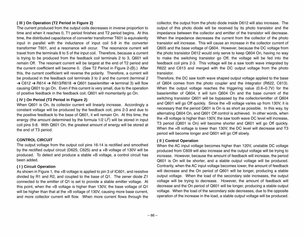
66
( lll ) On Operation (T2 Period in Figure 2)The current produced from the output coils decreases in inverse proportion totime and when it reaches 0, T1 period finishes and T2 period begins. At thistime, the distributed capacitance of converter transformer T601 is equivalentlyinput in parallel with the inductance of input coil 5-8 in the convertertransformer T601, and a resonance will occur. The resonance current willtravel from the terminals 8 to 5 of the input coil. Therefore, because a currentis trying to be produced from the feedback coil terminals 2 to 3, Q601 willremain Off. The resonant current will be largest at the end of T2 period andthe current coefficient will become 0. (See T2 Period in Figure 2-(B).) Afterthis, the current coefficient will reverse the polarity. Therefore, a current willbe produced in the feedback coil terminals 3 to 2 and the current (terminal 2 C612 R614 R613/R618 Q601 base/emitter terminal 3) will flowcausing Q601 to go On. Even if this current is very small, due to the operationof positive feedback in the feedback coil, Q601 will momentarily go On.
( lV ) On Period (T3 Period in Figure 2)When Q601 is On, its collector current will linearly increase. Accordingly aconstant voltage will be produced by the feedback coil, pins 2-3 and due tothe positive feedback to the base of Q601, it will remain On. At this time, theenergy (the amount determined by the formula 1/2 Ll2) will be stored in inputcoil pins 5-8. With Q601 On, the greatest amount of energy will be stored atthe end of T3 period.
CONTROL CIRCUITThe output voltage from the output coil pins 16-14 is rectified and smoothedby the rectified output circuit (D625, C625) and a +B voltage of 130V will beproduced. To detect and produce a stable +B voltage, a control circuit hasbeen added.
( l ) Circuit OperationAs shown in Figure 1, the +B voltage is applied to pin 3 of IC601, and resistivedivided by R1 and R2, and coupled to the base of Q1. The zener diode Z1connected to the emitter of Q1 is set to provide a stable emitter voltage. Atthis point, when the +B voltage is higher than 130V, the base voltage of Q1will be higher than that at the +B voltage of 130V, causing more base current,and more collector current will flow. When more current flows through the
collector, the output from the photo diode inside D612 will also increase. Theoutput of this photo diode will be received by its photo transistor and theimpedance between the collector and emitter of the transistor will decrease.When the impedance decreases the current from the collector of the phototransistor will increase. This will cause an increase in the collector current ofQ605 and the base voltage of Q604. However, because the DC voltage fromthe photo transistor D612 would only serve to keep Q604 On, having no wayto make the switching transistor go Off, the voltage will be fed into thefeedback coil pins 2-3. This voltage will be a saw tooth wave integrated byR622 and C613 and merged with the DC output voltage from the phototransistor.Therefore, the DC saw tooth wave shaped output voltage applied to the baseof Q604 comes from the photo coupler and the integrator (R622, C613).When the output voltage reaches the triggering value (0.6~0.7V) for thebase/emitter of Q604, it will turn Q604 On and the base current of theswitching transistor Q601 will be bypassed by the collector/emitter of Q604and Q601 will go Off quickly. Since the +B voltage varies up from 130V, it isnecessary that the period Q601 is On is as short as possible. In this way, byalternating Q604 On, and Q601 Off control is achieved. In other words, whenthe +B voltage is higher than 130V, the saw tooth wave DC level will increase,T3 period (Q601 is On) will become shorter and Q601 will go Off quickly.When the +B voltage is lower than 130V, the DC level will decrease and T3period will become longer and Q601 will go Off slowly.
( ll ) Control OperationWhen the AC input voltage becomes higher than 120V, unstable DC voltageproduced from C609 will also increase and the output voltage will be trying toincrease. However, because the amount of feedback will increase, the periodQ601 is On will be shorter, and a stable output voltage will be produced.Contrarily, when the AC input voltage becomes lower, the amount of feedbackwill decrease and the On period of Q601 will be longer, producing a stableoutput voltage. When the load of the secondary side increases, the outputvoltage will be trying to decrease. However, the amount of feedback willdecrease and the On period of Q601 will be longer, producing a stable outputvoltage. When the load of the secondary side decreases, due to the oppositeoperation of the increase in the load, a stable output voltage will be produced.

67
Figure 2. Waveforms in Power Supply Circuits
Q601 OFF PERIOD
Q601 ON OPERATIONQ601 ON PERIOD
T1 T3T2
RESONANTCURRENT
POSITIVEFEEDBACKVOLTAGE
OUTPUTVOLTAGE
0V
0A
0A
0V
(A) Q601 COLLECTOR EMITTER VOLTAGE
(B) T601 TERMINAL CURRENT
(C) Q601 COLLECTOR CURRENT
(D) T601 TERMINAL VOLTAGE
(E) T601 TERMINAL CURRENT
0A
(F) T601 TERMINAL VOLTAGE
(G) Q604 BASE ~ EMITTER VOLTAGE
T1 T3T2
I
Q601 OFF PERIOD
Q601 ON OPERATIONQ601 ON PERIOD
0V
0V
0A
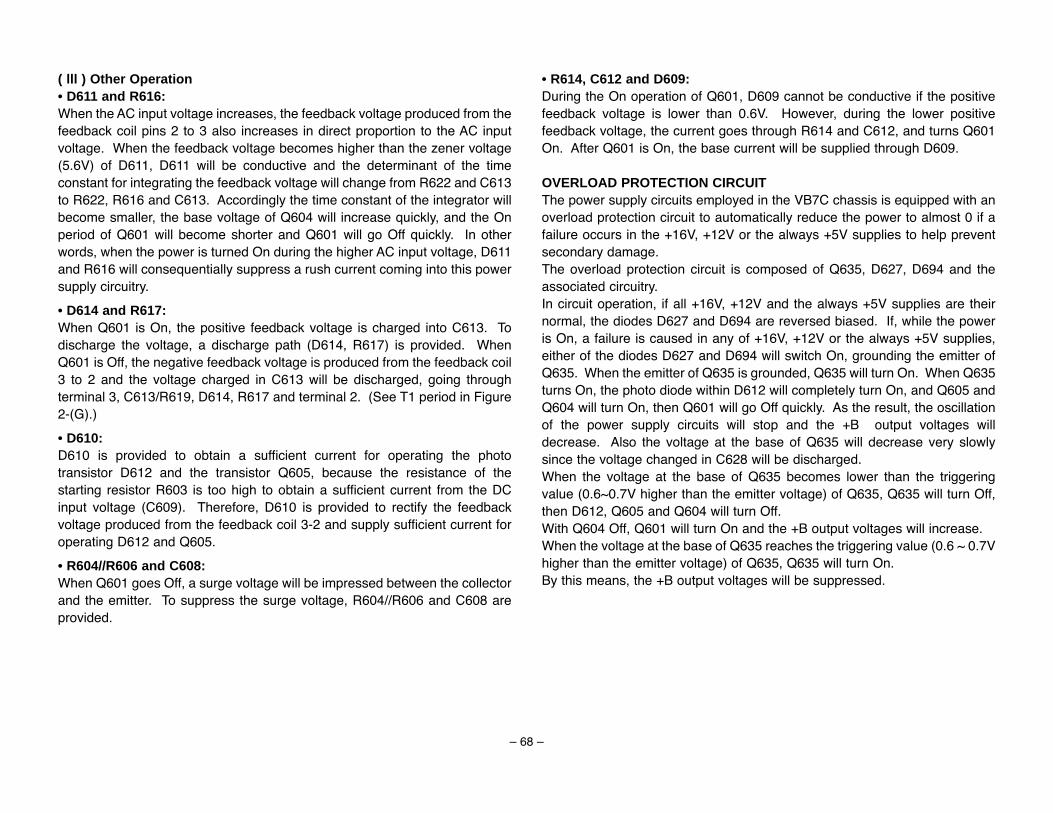
68
( lll ) Other Operation• D611 and R616:When the AC input voltage increases, the feedback voltage produced from thefeedback coil pins 2 to 3 also increases in direct proportion to the AC inputvoltage. When the feedback voltage becomes higher than the zener voltage(5.6V) of D611, D611 will be conductive and the determinant of the timeconstant for integrating the feedback voltage will change from R622 and C613to R622, R616 and C613. Accordingly the time constant of the integrator willbecome smaller, the base voltage of Q604 will increase quickly, and the Onperiod of Q601 will become shorter and Q601 will go Off quickly. In otherwords, when the power is turned On during the higher AC input voltage, D611and R616 will consequentially suppress a rush current coming into this powersupply circuitry.
• D614 and R617:When Q601 is On, the positive feedback voltage is charged into C613. Todischarge the voltage, a discharge path (D614, R617) is provided. WhenQ601 is Off, the negative feedback voltage is produced from the feedback coil3 to 2 and the voltage charged in C613 will be discharged, going throughterminal 3, C613/R619, D614, R617 and terminal 2. (See T1 period in Figure2-(G).)
• D610:D610 is provided to obtain a sufficient current for operating the phototransistor D612 and the transistor Q605, because the resistance of thestarting resistor R603 is too high to obtain a sufficient current from the DCinput voltage (C609). Therefore, D610 is provided to rectify the feedbackvoltage produced from the feedback coil 3-2 and supply sufficient current foroperating D612 and Q605.
• R604//R606 and C608:When Q601 goes Off, a surge voltage will be impressed between the collectorand the emitter. To suppress the surge voltage, R604//R606 and C608 areprovided.
• R614, C612 and D609:During the On operation of Q601, D609 cannot be conductive if the positivefeedback voltage is lower than 0.6V. However, during the lower positivefeedback voltage, the current goes through R614 and C612, and turns Q601On. After Q601 is On, the base current will be supplied through D609.
OVERLOAD PROTECTION CIRCUITThe power supply circuits employed in the VB7C chassis is equipped with anoverload protection circuit to automatically reduce the power to almost 0 if afailure occurs in the +16V, +12V or the always +5V supplies to help preventsecondary damage. The overload protection circuit is composed of Q635, D627, D694 and theassociated circuitry.In circuit operation, if all +16V, +12V and the always +5V supplies are theirnormal, the diodes D627 and D694 are reversed biased. If, while the poweris On, a failure is caused in any of +16V, +12V or the always +5V supplies,either of the diodes D627 and D694 will switch On, grounding the emitter ofQ635. When the emitter of Q635 is grounded, Q635 will turn On. When Q635turns On, the photo diode within D612 will completely turn On, and Q605 andQ604 will turn On, then Q601 will go Off quickly. As the result, the oscillationof the power supply circuits will stop and the +B output voltages willdecrease. Also the voltage at the base of Q635 will decrease very slowlysince the voltage changed in C628 will be discharged.When the voltage at the base of Q635 becomes lower than the triggeringvalue (0.6~0.7V higher than the emitter voltage) of Q635, Q635 will turn Off,then D612, Q605 and Q604 will turn Off.With Q604 Off, Q601 will turn On and the +B output voltages will increase.When the voltage at the base of Q635 reaches the triggering value (0.6 ~ 0.7Vhigher than the emitter voltage) of Q635, Q635 will turn On.By this means, the +B output voltages will be suppressed.

69
POWER SAVING CIRCUITThe power supply circuits employed in the VB7C chassis are equipped withthe interval oscillation circuit for saving the power consumed during the stand-by mode.The interval oscillation circuit is composed of Q693, Q695, D693 and theassociated circuitry.When the TV is turned Off, the voltage at point (A) is almost 0V, and Q693 andQ695 remain Off. When the TV set is turned On, the voltage at point (A) willincrease to approximately 12V. The voltage is resistive divided by R692 andR693 and applied the base of Q693, then Q693 and Q695 will turn On. WhenQ695 turns On, the photo divide within D612 will completely turn On, andQ605 and Q604 will turn On, then the switching transistor Q601 will turn Off.
As a result, the oscillation of the power supply circuits will stop and the outputvoltages of the power supply circuits will fall down. Also the voltage at point(A) will gradually fall down from 12V. When the voltage at the base of Q693becomes lower than the triggering value (0.6~0.7V higher than emittervoltage) of Q693, Q693 will turn Off, then Q695, D612, Q605 and Q604 willturn Off.As a result, Q601 will start oscillation and the output voltages of the powersupply circuits will be supplied.By this means, the voltage at point (A) will increase and turn Q693 On again.By repeating the above operation, power consumption during the stand-bymode can be reduced.
Operating period of Power Supply Circuits
12 V
0 VVoltage at point A
Figure 3. Interval Oscillation

70
CPU TROUBLESHOOTING HINTSDescribed in this section are some suggested techniques for discoveringdefects in the frequency synthesizer and CPU controlled circuits. An isolationtransformer should always be used when servicing the TV to prevent possibleelectrical shock (Hot Chassis) and equipment damage. When connecting anyequipment to a circuit, start by connecting the negative side. This will reducethe possibility of damage to semiconductors and IC chips.
When determining the cause of a trouble by checking a waveform, starttracing it down from the output or input end of the signal system to facilitatethis work. This will help you discover in which circuit the cause of trouble islocated.
The troubleshooting hints included here do not include all possible defectsthat may be encountered. This section is only intended to be a guide. Alwaysrefer to the service literature for the specifications, parts lists, and safetyrelated items. DO NOT defeat any safety items or features.
Dead1. Check the 5 volt power supply (IC801, pins 14 and 22).
A. If no 5 volt supply, check IC681 and D624.2. Check reset terminal (IC801, pin 25) for 5 volts.
A. If no 5 volts, check Q831.3. Check operation of clock oscillator (IC801, pins 19-20).
A. Check X801.B. Check IC801.
4. Check for a LOW to HIGH state change (IC801, pin 27) with operation ofthe power key.A. If no change, check all keys for stuck-closed condition.B. Check remote operation.C. Check IC801.
5. If pin 27 of IC801 changes from a LOW to a HIGH state, check +12VSwitch Drive Transistor Q681 and +12V Switch Transistor Q627.
No Remote Operation (Manual Operation OK)1. Check for 5 volts on pin 2 of RC Pre-Amp (A1901).2. With an oscilloscope, check for output pulses on pin 1 of A1901 with
operation of a known good remote.3. Check IC801.
No Manual Operation (Remote Operation OK)1. Check for correct voltage changes at pin 9 of IC801. (Check while
pressing keys).2. Check IC801.
Display1. If incorrect position or no display, check Q881 and Q882 for proper sync
pulses.2. If no display, check IC801, pin 17 for proper sync pulses in the composite
video signal.3. Check IC801, pins 39-42 for 5Vp-p pulses.4. Check IC101.
Audio1. With an oscilloscope, check for audio output signal on pins 3 and 4 of
IC3401 while pressing volume keys.A. If signal is normal, check IC001 and/or associated circuitry.B. Check IC801.
AFT1. Check PLL Tuning alignment per service literature.2. Check for correct operation of TB circuitry (Q371, Q372).3. Check IC801.
Tuning (Cannot Receive Stations)1. Check IC801, pins 32 and 34 for 5Vp-p pulses.2. Check Tuner voltages and Tuner.
A. If tuning voltage (TU) changes when selecting different channels,problem is with tuner and/or associated circuitry.

71
No MTS Function1. While receiving known stereo and SAP signals, check for audio output
signals on pins 3, 4, 38 and 39 of IC 3401 with and oscilloscope.A. If signal is not normal, problem is with MTS Processor (IC3401) and/orassociated circuitry.
2. Check Multi-Sound Section alignment per service manual.
No Caption1. While receiving known Caption encoded signals, check CPU pins 39-42
for 5Vp-p pulses and recheck Captions Menu.2. Check CPU pin 17 for 2 Vp-p composite video.
No AV1. Check for proper Low to High switching when selecting AV mode on CPU
pins 7 and 8. (See page 24 for TV/AV Switching Circuits.)A. If CPU pins 7 and 8 do not switch correctly, check IC801.B. If pins 7 and 8 switch correctly, check IC101, IC1001, IC1002, IC1081for video signal switching and IC3401 for audio signal switching.
No S-Video1. Check for proper Low to High switching at IC1081 pins 9 and 10 when
connecting known S-Video signal to S-Video Input jack.A. If pins 9-10 do not switch correctly, check IC801 and IC1081.
Color Enhancer1. With an oscilloscope, check for R and B output signals on pins 28 and 30
of IC101 when selecting Warm mode.A. If pins 28 and 30 do not change, check IC101 and IC801.
No PIP Picture1. Check PIP 3.3 volt power supply (Q8000, emitter).
A. If no 3.3 volt power supply, check Q8000.2. Check for clock pulses and PIP control data at IC8001, pins 24-25.
A. If signals are correct, check IC8001.B. If signals are not correct, check IC801.
3. Check for vertical and horizontal sync pulses at IC8001, pins 32-33.A. If pulses are correct, check IC8001.B. If pulses are not correct, check Q881, Q882, Q8005 and Q8006 forproper sync pulses.
4. Check for TV or AV video signal at IC8001, pin 13.A. If signals are correct, check IC8001.B. If TV video signal is not correct, check IC1002, Q162 and IC101 for
proper TV video signal.C. If AV video signal is not correct, check IC1002, Q1093, Q1094 and
Q1096 for proper video input from external equipment.

72
1
2
4
3
5
6
7
8
9
10
11
12
14
13
15
16
17
18
19
20
21
42
41
39
40
38
37
36
35
34
32
31
30
28
29
27
26
25
24
23
22
33
H-SYNC
V-SYNC
POWER FAIL
MAIN S SELECT
MAIN AV1/AV2
PIP AV1/AV2
PIP TV/AV
MAIN TV/VIDEO
KEY SCAN IN
REMOTE CONTROL IN
N/A (Open)
S1 DETECT SW
CVIN
N/A (Open)
AVcc (+5V)
X IN
V HOLD IN
Vss (GND)
R
G
B
BLK
MUTE
ACK
STATUS
S2 DEFEAT SW
BUS SCL
IIC SCL
IIC SDA
AFT S-CURVE
RF AGC
POWER
TIME BASE
RESET
N/A (Pull Down)
AC 50/60Hz (Open)
Vcc (+5V)
ABL-IN
CPU Pin Allotment
HLF
CNVss (GND)
X OUT
BUS SDA
( I )
( I )
( I )
(O)
(O)
(O)
(O)
(O)
( I )
( I )
( I )
(O)
(O)
(O)
(O)
(O)
( I )
( I )
(I/O)
(I/O)
( I )
( I )
(O)
( I )
( I )
( I )
(O)
(O)
( I )
(O)
( I )
(O)
( I )
( I )
(O)
( I )
( )
( )
(O)
( )
( )
( I )
Top Related