


Languages
Pages
Legal


Visit analog.com
POWERING ADI COMPONENTSIn Industrial and Instrumentation Applications
2 Powering ADI Components Visit analog.com 3 2 Powering ADI Components Visit analog.com 3
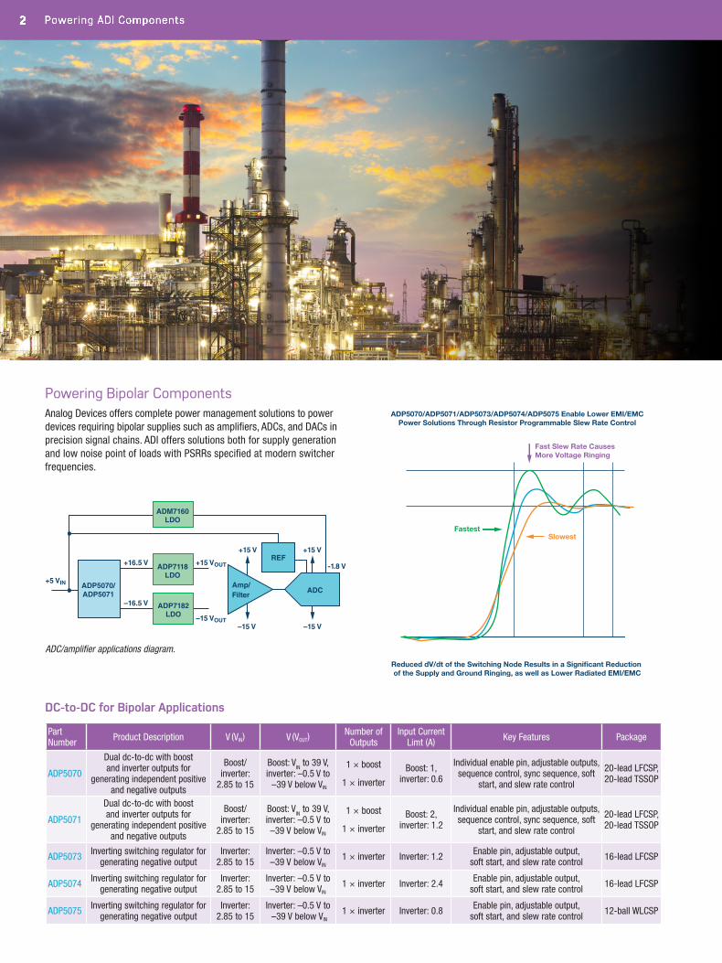
Powering Bipolar ComponentsAnalog Devices offers complete power management solutions to power devices requiring bipolar supplies such as amplifiers, ADCs, and DACs in precision signal chains. ADI offers solutions both for supply generation and low noise point of loads with PSRRs specified at modern switcher frequencies.
ADP5070/ADP5071
ADP7118LDO
+16.5 V
+5 VIN
–16.5 V
+15 VOUT
+15 V
–15 VOUT–15 V
Amp/Filter
ADC
REF-1.8 V
+15 V
–15 V
ADP7182LDO
ADM7160LDO
ADC/amplifier applications diagram.
DC-to-DC for Bipolar Applications
Part Number Product Description V (VIN) V (VOUT)
Number of Outputs
Input Current Limt (A) Key Features Package
ADP5070
Dual dc-to-dc with boost and inverter outputs for
generating independent positive and negative outputs
Boost/ inverter:
2.85 to 15
Boost: VIN to 39 V,
inverter: –0.5 V to –39 V below VIN
1 × boost
1 × inverter
Boost: 1, inverter: 0.6
Individual enable pin, adjustable outputs, sequence control, sync sequence, soft
start, and slew rate control
20-lead LFCSP, 20-lead TSSOP
ADP5071
Dual dc-to-dc with boost and inverter outputs for
generating independent positive and negative outputs
Boost/inverter:
2.85 to 15
Boost: VIN to 39 V,
inverter: –0.5 V to –39 V below VIN
1 × boost
1 × inverter
Boost: 2, inverter: 1.2
Individual enable pin, adjustable outputs, sequence control, sync sequence, soft
start, and slew rate control
20-lead LFCSP, 20-lead TSSOP
ADP5073 Inverting switching regulator for generating negative output
Inverter: 2.85 to 15
Inverter: –0.5 V to –39 V below VIN
1 × inverter Inverter: 1.2 Enable pin, adjustable output, soft start, and slew rate control 16-lead LFCSP
ADP5074 Inverting switching regulator for generating negative output
Inverter: 2.85 to 15
Inverter: –0.5 V to –39 V below VIN
1 × inverter Inverter: 2.4 Enable pin, adjustable output, soft start, and slew rate control 16-lead LFCSP
ADP5075 Inverting switching regulator for generating negative output
Inverter: 2.85 to 15
Inverter: –0.5 V to –39 V below VIN
1 × inverter Inverter: 0.8 Enable pin, adjustable output, soft start, and slew rate control 12-ball WLCSP
ADP5070/ADP5071/ADP5073/ADP5074/ADP5075 Enable Lower EMI/EMCPower Solutions Through Resistor Programmable Slew Rate Control
Fastest
Fast Slew Rate CausesMore Voltage Ringing
Slowest
Reduced dV/dt of the Switching Node Results in a Significant Reduction of the Supply and Ground Ringing, as well as Lower Radiated EMI/EMC
2 Powering ADI Components Visit analog.com 3 2 Powering ADI Components Visit analog.com 3
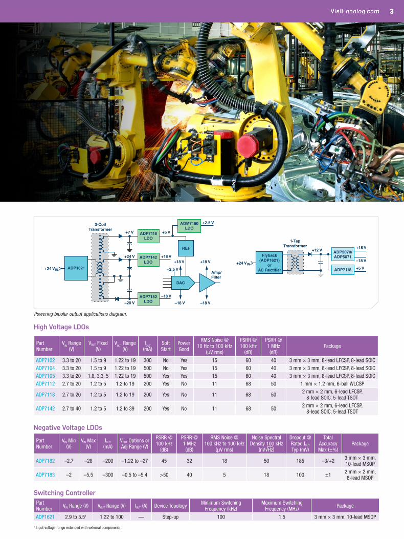
+24 VIN ADP1621
3-CoilTransformer
–18 V
–18 V
+18 V
–18 V
+18 V+18 V
+5 V
+2.5 V
+2.5 V
–20 V
DAC
REF
Amp/Filter
+24 V
+7 V ADP7118LDO
ADM7160LDO
ADP7142LDO
ADP7182LDO
High Voltage LDOs
Part Number
VIN Range (V)
VOUT Fixed (V)
VOUT
Range (V)
IOUT
(mA) Soft Start
Power Good
RMS Noise @ 10 Hz to 100 kHz
(μV rms)
PSRR @ 100 kHz
(dB)
PSRR @ 1 MHz (dB)
Package
ADP7102 3.3 to 20 1.5 to 9 1.22 to 19 300 No Yes 15 60 40 3 mm × 3 mm, 8-lead LFCSP, 8-lead SOIC
ADP7104 3.3 to 20 1.5 to 9 1.22 to 19 500 No Yes 15 60 40 3 mm × 3 mm, 8-lead LFCSP, 8-lead SOIC
ADP7105 3.3 to 20 1.8, 3.3, 5 1.22 to 19 500 Yes Yes 15 60 40 3 mm × 3 mm, 8-lead LFCSP, 8-lead SOIC
ADP7112 2.7 to 20 1.2 to 5 1.2 to 19 200 Yes No 11 68 50 1 mm × 1.2 mm, 6-ball WLCSP
ADP7118 2.7 to 20 1.2 to 5 1.2 to 19 200 Yes No 11 68 50 2 mm × 2 mm, 6-lead LFCSP, 8-lead SOIC, 5-lead TSOT
ADP7142 2.7 to 40 1.2 to 5 1.2 to 39 200 Yes No 11 68 50 2 mm × 2 mm, 6-lead LFCSP, 8-lead SOIC, 5-lead TSOT
Negative Voltage LDOs
Part Number
VIN Min (V)
VIN Max (V)
IOUT (mA)
VOUT Options or Adj Range (V)
PSRR @ 100 kHz
(dB)
PSRR @ 1 MHz (dB)
RMS Noise @ 100 kHz to 100 kHz
(μV rms)
Noise Spectral Density 100 kHz
(nV√Hz)
Dropout @ Rated IOUT Typ (mV)
Total Accuracy Max (±%)
Package
ADP7182 –2.7 –28 –200 –1.22 to –27 45 32 18 50 185 –3/+2 3 mm × 3 mm, 10-lead MSOP
ADP7183 –2 –5.5 –300 –0.5 to –5.4 >50 40 5 18 100 ±1 2 mm × 2 mm, 8-lead MSOP
Switching ControllerPart Number VIN Range (V) VOUT Range (V) IOUT (A) Device Topology Minimum Switching
Frequency (kHz)Maximum Switching
Frequency (MHz) Package
ADP1621 2.9 to 5.51 1.22 to 100 — Step-up 100 1.5 3 mm × 3 mm, 10-lead MSOP
1 Input voltage range extended with external components.
+5 V
–18 V
+18 V
+24 VIN
Flyback(ADP1621)
orAC Recti�er
1-TapTransformer
+12 V ADP5070/ADP5071
ADP7118
Powering bipolar output applications diagram.
4 Powering ADI Components 4 Powering ADI Components
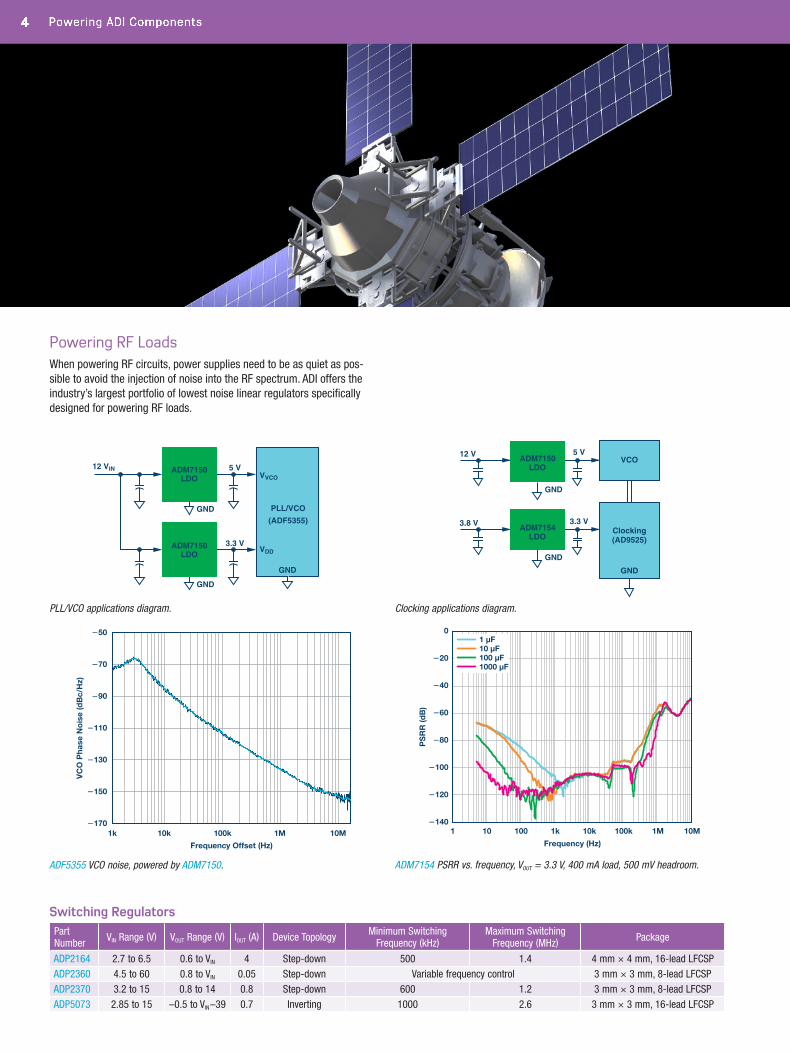
12 VIN 5 V
3.3 V
ADM7150VVCO
VDDADM7150
PLL/VCO
(ADF5355)
LDO
LDO
GND
GND
GND
3.8 V 3.3 VADM7154 Clocking
(AD9525)
GND
LDO
GND
12 V 5 VADM7150
GND
LDOVCO
Powering RF LoadsWhen powering RF circuits, power supplies need to be as quiet as pos-sible to avoid the injection of noise into the RF spectrum. ADI offers the industry’s largest portfolio of lowest noise linear regulators specifically designed for powering RF loads.
−50
−70
−170
−150
−130
−110
−90
1k 10k 100k 1M 10M
VC
O P
hase
No
ise
(dB
c/H
z)
Frequency Offset (Hz)
PS
RR
(dB
)
Frequency (Hz)
10M1 10 100 1k 10k 100k 1M−140
−120
−100
−80
−60
−40
−20
01 µF10 µF100 µF1000 µF
PLL/VCO applications diagram. Clocking applications diagram.
ADF5355 VCO noise, powered by ADM7150. ADM7154 PSRR vs. frequency, VOUT = 3.3 V, 400 mA load, 500 mV headroom.
Switching RegulatorsPart Number VIN Range (V) VOUT Range (V) IOUT (A) Device Topology Minimum Switching
Frequency (kHz)Maximum Switching
Frequency (MHz) Package
ADP2164 2.7 to 6.5 0.6 to VIN 4 Step-down 500 1.4 4 mm × 4 mm, 16-lead LFCSPADP2360 4.5 to 60 0.8 to VIN 0.05 Step-down Variable frequency control 3 mm × 3 mm, 8-lead LFCSPADP2370 3.2 to 15 0.8 to 14 0.8 Step-down 600 1.2 3 mm × 3 mm, 8-lead LFCSP
ADP5073 2.85 to 15 –0.5 to VIN–39 0.7 Inverting 1000 2.6 3 mm × 3 mm, 16-lead LFCSP
Visit analog.com 5 Visit analog.com 5
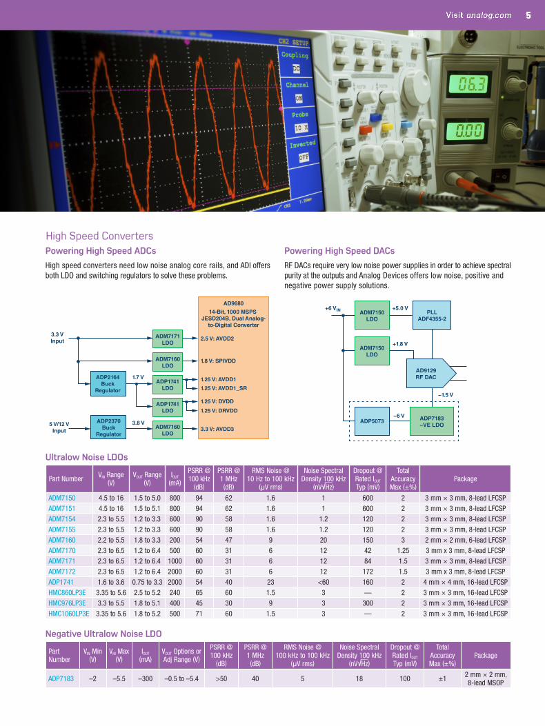
High Speed ConvertersPowering High Speed ADCs
High speed converters need low noise analog core rails, and ADI offers both LDO and switching regulators to solve these problems.
2.5 V: AVDD2
1.8 V: SPIVDD
AD9680
1.25 V: AVDD1
14-Bit, 1000 MSPS JESD204B, Dual Analog-
to-Digital Converter
1.25 V: AVDD1_SR
ADP2164Buck
Regulator
ADP2370Buck
Regulator
1.25 V: DVDD
1.25 V: DRVDD
3.3 V: AVDD33.8 V
1.7 V
5 V/12 VInput
3.3 VInput
ADP1741LDO
ADP1741LDO
ADM7171LDO
ADM7160LDO
ADM7160LDO
Powering High Speed DACs
RF DACs require very low noise power supplies in order to achieve spectral purity at the outputs and Analog Devices offers low noise, positive and negative power supply solutions.
ADM7150LDO
PLLADF4355-2
AD9129RF DAC
ADP7183−VE LDO
−1.5 V
−6 V
+6 VIN +5.0 V
+1.8 VADM7150
LDO
ADP5073
Ultralow Noise LDOs
Part Number VIN Range (V)
VOUT Range (V)
IOUT
(mA)
PSRR @ 100 kHz
(dB)
PSRR @ 1 MHz (dB)
RMS Noise @ 10 Hz to 100 kHz
(μV rms)
Noise Spectral Density 100 kHz
(nV√Hz)
Dropout @ Rated IOUT Typ (mV)
Total Accuracy Max (±%)
Package
ADM7150 4.5 to 16 1.5 to 5.0 800 94 62 1.6 1 600 2 3 mm × 3 mm, 8-lead LFCSP
ADM7151 4.5 to 16 1.5 to 5.1 800 94 62 1.6 1 600 2 3 mm × 3 mm, 8-lead LFCSP
ADM7154 2.3 to 5.5 1.2 to 3.3 600 90 58 1.6 1.2 120 2 3 mm × 3 mm, 8-lead LFCSP
ADM7155 2.3 to 5.5 1.2 to 3.3 600 90 58 1.6 1.2 120 2 3 mm × 3 mm, 8-lead LFCSP
ADM7160 2.2 to 5.5 1.8 to 3.3 200 54 47 9 20 150 3 2 mm × 2 mm, 6-lead LFCSP
ADM7170 2.3 to 6.5 1.2 to 6.4 500 60 31 6 12 42 1.25 3 mm x 3 mm, 8-lead LFCSP
ADM7171 2.3 to 6.5 1.2 to 6.4 1000 60 31 6 12 84 1.5 3 mm × 3 mm, 8-lead LFCSP
ADM7172 2.3 to 6.5 1.2 to 6.4 2000 60 31 6 12 172 1.5 3 mm x 3 mm, 8-lead LFCSP
ADP1741 1.6 to 3.6 0.75 to 3.3 2000 54 40 23 <60 160 2 4 mm × 4 mm, 16-lead LFCSP
HMC860LP3E 3.35 to 5.6 2.5 to 5.2 240 65 60 1.5 3 — 2 3 mm × 3 mm, 16-lead LFCSP
HMC976LP3E 3.3 to 5.5 1.8 to 5.1 400 45 30 9 3 300 2 3 mm × 3 mm, 16-lead LFCSP
HMC1060LP3E 3.35 to 5.6 1.8 to 5.2 500 71 60 1.5 3 — 2 3 mm × 3 mm, 16-lead LFCSP
Negative Ultralow Noise LDO
Part Number
VIN Min (V)
VIN Max (V)
IOUT (mA)
VOUT Options or Adj Range (V)
PSRR @ 100 kHz
(dB)
PSRR @ 1 MHz (dB)
RMS Noise @ 100 kHz to 100 kHz
(μV rms)
Noise Spectral Density 100 kHz
(nV√Hz)
Dropout @ Rated IOUT Typ (mV)
Total Accuracy Max (±%)
Package
ADP7183 –2 –5.5 –300 –0.5 to –5.4 >50 40 5 18 100 ±1 2 mm × 2 mm, 8-lead MSOP

6 Powering ADI Components
Typical application circuits.
ADP1761/ADP1762/ADP1763 X 1 A, 2 A, and 3 A versions available
Ultralow Dropout Voltage
X 80 mV @ 2 A load
X ±1.5% accuracy over line, load, and temperature
Excellent PSRR Performance
X 55 dB @ 100 kHz @ 2 A load
X 40 dB @ 1 MHz @ 2 A load
X 16-lead, 3 mm × 3 mm LFCSP package
Upcoming Solutions for Powering High Speed Converters
VOUT
VOUT = 0.80 V
Sense
COUT10 µF
CIN10 µF
CREF1 µF
CREG1 µF
PGOOD
ADP1761/ADP1762/ADP1763
VADJ
REFCAP
GND
VREG
SS
ENOff
On
VIN
VIN = 1.1 VADI
High SpeedConverter
(ADC or DAC)
ADP7183 X Input voltage range:
–2 V to –5.5 V
X Max current rating: –300 mA
X Very low noise 5 μV rms independent of VOUT
X PSRR at 1 MHz 40 dB, 100 kHz >50 dB
X Fixed output voltage options: –0.5 V to –4.5 V
X Initial accuracy: ±0.5%
X Precision enable at –1.2 V
X Positive enable control
X 8-lead, 2 mm × 2 mm LFCSP
CIN10 µF
CBYP1 µF
CREG10 µF
1 µF
CFIL
+1.2 V
0 V–1.2 V
VIN = –5 V
Off
On
On
VOUT = –3.3 V
COUT10 µF
VA
Sense
VAFB
GND
VREG
EN
VOUTVIN8
7
6
5
1
2
3
4
ADIRF DAC
ADP5003
Low Noise Buck and LDO
X 3 A low noise buck regulator
X Buck wide input range: 4.2 V to 15 V
X Buck programmable output range: 0.6 V to 5 V
X <40 μV rms buck output noise (independent of VOUT setting)
X Internal 3 A, low noise NFET LDO acts as an active filter for sensitive analog supplies
X LDO wide input range: 0.65 V to 5 V
X LDO fixed/programmable output range: 0.6 V to 3.3 V
X True differential remote sensing
X Below 10 μV rms LDO output noise (independent of VOUT)
X PSRR >50 dB (up to 100 kHz) @ 200 mV headroom at 2 A
X Power-good output
EN1
EN2
BuckRegulator
3 A
System
Low Noise,LDO Active
Filter3 A
ADI RFTransceiver,
HS ADC/DAC,Clock, ASIC/Processor
AGND
PVIN1 VIN = 12 V
VFB1
SW1 L12.2 µH
PGND1
VMID(Adaptive)
SS/RT
PWRGD
Optional2nd Filter
SyncIN/SyncOUT
PVIN2
VOUT2 VOUT = 1.300 V(<10 µV rms, ±1.5%)
VFB2P
VFB2N
COMP
VSET1
VREG
VIN = 12 V PVINSYS
REFOUT
VSET2
VBUF
VREGLDO
Visit analog.com 7
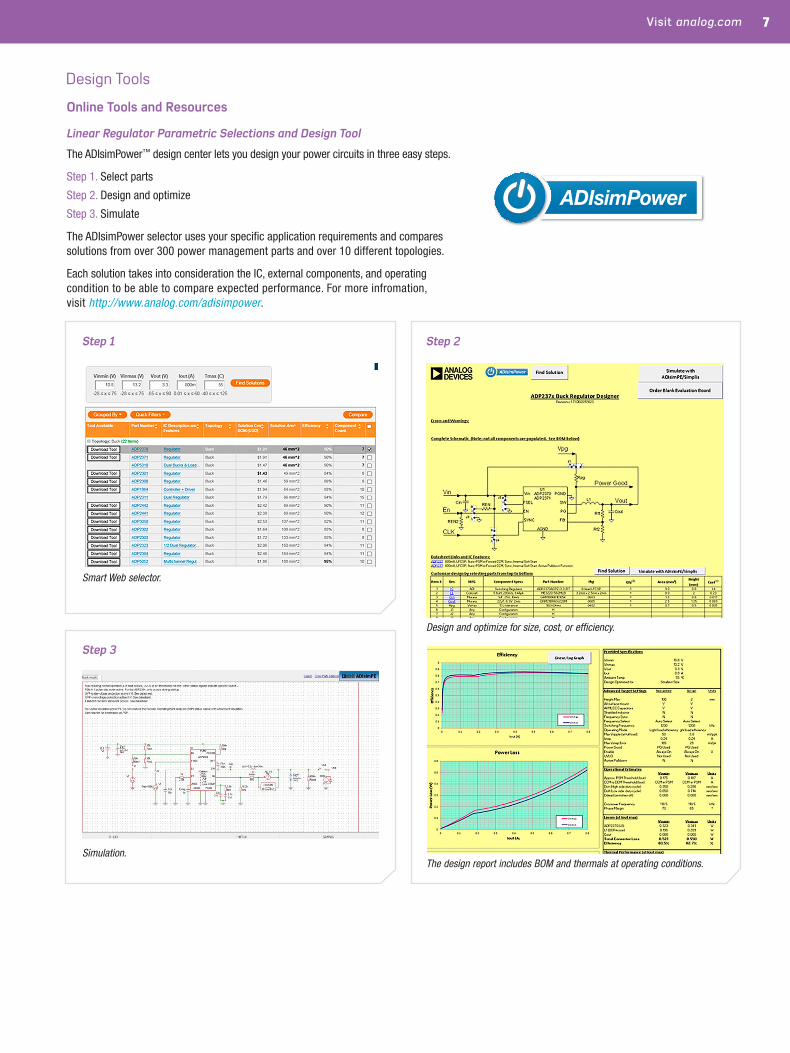
Step 3
Design Tools
Online Tools and Resources
Linear Regulator Parametric Selections and Design Tool
The ADIsimPower™ design center lets you design your power circuits in three easy steps.
Step 1. Select parts
Step 2. Design and optimize
Step 3. Simulate
The ADIsimPower selector uses your specific application requirements and compares solutions from over 300 power management parts and over 10 different topologies.
Each solution takes into consideration the IC, external components, and operating condition to be able to compare expected performance. For more infromation, visit http://www.analog.com/adisimpower.
Step 1 Step 2
Smart Web selector.
Design and optimize for size, cost, or efficiency.
The design report includes BOM and thermals at operating conditions.Simulation.
Analog Devices, Inc. Worldwide Headquarters
Analog Devices, Inc. One Technology Way P.O. Box 9106 Norwood, MA 02062-9106 U.S.A. Tel: 781.329.4700 (800.262.5643, U.S.A. only) Fax: 781.461.3113
Analog Devices, Inc. Europe Headquarters
Analog Devices, Inc. Wilhelm-Wagenfeld-Str. 6 80807 Munich Germany Tel: 49.89.76903.0 Fax: 49.89.76903.157
Analog Devices, Inc. Japan Headquarters
Analog Devices, KK New Pier Takeshiba South Tower Building 1-16-1 Kaigan, Minato-ku, Tokyo, 105-6891 Japan Tel: 813.5402.8200 Fax: 813.5402.1064
Analog Devices, Inc. Asia Pacific Headquarters
Analog Devices 5F, Sandhill Plaza 2290 Zuchongzhi Road Zhangjiang Hi-Tech Park Pudong New District Shanghai, China 201203 Tel: 86.21.2320.8000 Fax: 86.21.2320.8222
©2016 Analog Devices, Inc. All rights reserved. Trademarks and registered trademarks are the property of their respective owners.Ahead of What’s Possible is a trademark of Analog Devices.BR13573-2.5-2/16
analog.com
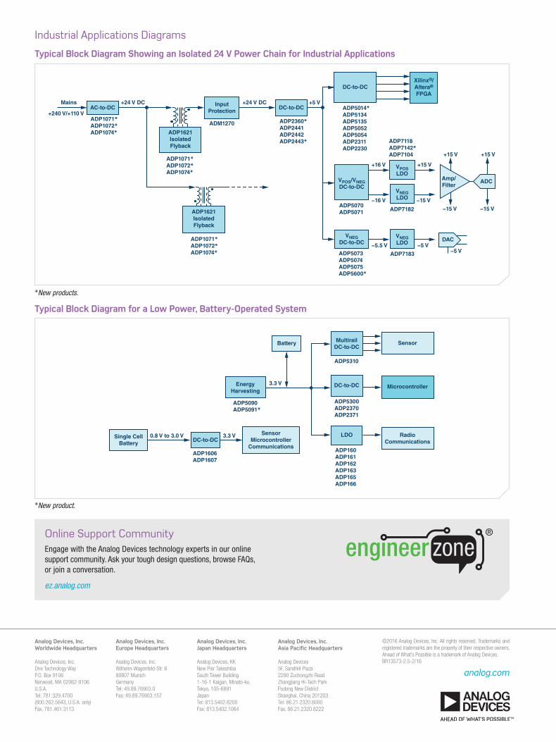
Industrial Applications Diagrams
Typical Block Diagram Showing an Isolated 24 V Power Chain for Industrial Applications
Mains
+240 V/+110 V
+24 V DC +24 V DC +5 V
+16 V
−16 V
+15 V
−15 V
+15 V
−15 V
+15 V
−15 V
ADP1621IsolatedFlyback
AC-to-DC
ADM1270
InputProtection
ADP2360*ADP2441ADP2442ADP2443*
DC-to-DC ADP5014*ADP5134ADP5135ADP5052ADP5054ADP2311ADP2230
DC-to-DC
Amp/Filter
ADC
ADP5070ADP5071 ADP7182
ADP7183
ADP7118ADP7142*ADP7104
VPOSLDO
VNEGLDO
−5.5 V −5 V
VNEGLDO
VPOS/VNEGDC-to-DC
VNEGDC-to-DC
Xilinx®/Altera®
FPGA
ADP1071*ADP1072*ADP1074*
ADP1071*ADP1072*ADP1074*
ADP1621IsolatedFlyback
ADP1071*ADP1072*ADP1074*
DAC
−5 VADP5073ADP5074ADP5075ADP5600*
*New products.
Typical Block Diagram for a Low Power, Battery-Operated System
SensorBattery
Single CellBattery
3.3 V
3.3 V0.8 V to 3.0 V
EnergyHarvesting
Microcontroller
SensorMicrocontroller
Communications
RadioCommunications
ADP5310
ADP5090ADP5091*
ADP1606ADP1607
ADP5300ADP2370ADP2371
ADP160ADP161ADP162ADP163ADP165ADP166
MultirailDC-to-DC
DC-to-DC
DC-to-DCLDO
*New product.
Online Support CommunityEngage with the Analog Devices technology experts in our online support community. Ask your tough design questions, browse FAQs, or join a conversation.
ez.analog.com
Top Related