


Languages
Pages
Legal


nature materials | VOL 9 | MARCH 2010 | www.nature.com/naturematerials 193
review articlePublished online: 19 february 2010 | doi: 10.1038/nmat2630
Plasmonics is a flourishing new field of science and technology that exploits the unique optical properties of metallic nanostructures to route and manipulate light at nanometre length
scales. Nanometallic objects derive their properties from an ability to support collective electron excitations, known as surface plasmons. At present, plasmonics research enables new fundamental science and device technologies, and we are witnessing a dramatic growth in both the number and scope of plasmonic applications. Plasmonics may soon become a pervasive technology, offering unusual optical capabilities and a tantalizing opportunity to attain unprecedented levels of synergy between optical and electronic functions. Although resistive heating losses in metals can severely limit the performance of devices that depend critically on longdistance propagation of surface plasmon waves (surface plasmon polaritons or SPPs), many useful functionalities have recently been realized despite the presence of loss. The most successful ones tend to use structures for extreme light concentration; plasmonic antennas, lenses and resonators provide excellent examples.
The ability to concentrate light and/or produce high localfield intensities has traditionally been the domain of dielectric lenses and resonators. These objects provide a convenient way to manipulate light and enhance a range of linear and nonlinear phenomena. Owing to the fundamental laws of diffraction, dielectric lenses cannot focus light to spots less than about half a wavelength of light (~λ/2) and dielectric resonators have electromagnetic mode volumes (vm) limited to vm ~ (λ/2)3, where λ is the wavelength of light inside the dielectric medium. The nature of nanometallic light concentrators and resonators is distinct from their dielectric counterparts, and nanometallic structures do not have these limitations. Plasmonic antennas and lenses can convert optical radiation into intense, engineered, localized field distributions or enable coupling to deepsubwavelengthguided modes. Thus, wherever subwavelength control over light is desired, nanometallic structures are likely to play an important part. By squeezing light into subwavelength volumes, plasmonic structures can efficiently mediate interactions between propagating radiation and nanoscale objects and devices. The first part of this article summarizes the fundamentals behind such plasmonic light concentrators and reviews their use in imaging techniques with improved spatial resolution, ultrafast and compact photodetectors and modulators,
Plasmonics for extreme light concentration and manipulationJon a. schuller, edward s. barnard, Wenshan Cai, young Chul Jun, Justin s. White and mark l. brongersma*
The unprecedented ability of nanometallic (that is, plasmonic) structures to concentrate light into deep-subwavelength volumes has propelled their use in a vast array of nanophotonics technologies and research endeavours. Plasmonic light con-centrators can elegantly interface diffraction-limited dielectric optical components with nanophotonic structures. Passive and active plasmonic devices provide new pathways to generate, guide, modulate and detect light with structures that are similar in size to state-of-the-art electronic devices. With the ability to produce highly confined optical fields, the conventional rules for light–matter interactions need to be re-examined, and researchers are venturing into new regimes of optical physics. In this review we will discuss the basic concepts behind plasmonics-enabled light concentration and manipulation, make an attempt to capture the wide range of activities and excitement in this area, and speculate on possible future directions.
higher efficiency solar cells, and techniques for locally controlling catalytic and thermally stimulated processes.
As well as acting as an interface with the nanoscale, plasmonic structures can also change light–matter interactions at a very fundamental level. The possibility to confine light in subwavelength modevolume cavities has a profound effect on the efficacy of many optical processes that benefit from highopticalquality factors (Q) and ultrasmall vm. Despite modest values of Q (typically between 10–100), metallic cavities with sufficiently small mode volumes can often outperform much higher Q dielectric cavities (Q ~ 106) and benefit from having a more broadband response and easy electrical access. In the second part of this article, we review the use of plasmonic structures to enhance a range of nonlinear processes in ultracompact device geometries, modify the temporal and spatial properties of light emitters, control both near and farfield thermal radiation pathways, and manipulate light using new optical materials with engineered refractive indices.
In this review, we attempt to describe the very wide range of plasmonic research activities that involve extreme light concentration and manipulation. However, no review of a large field can be exhaustive and we have chosen not to discuss important efforts on plasmonbased sensors, which constitute a large body of research for which excellent recent reviews already exist1.
fundamentals of plasmonic light concentratorsResearchers are investigating the optical properties of an increasing variety of metallic nanostructures with the hope of effectively concentrating light into nanoscale volumes. The structures come in two distinct varieties: resonant and nonresonant. In resonant structures, timevarying electric fields associated with light waves exert a force on the gas of negatively charged electrons inside a metal and drive them into a collective oscillation, known as a surface plasmon. At specific optical frequencies this oscillation is resonantly driven to produce a very strong charge displacement and associated (light) field concentration. We will first discuss such resonant behaviour in quasistatic and retardationbased structures, before continuing with nonresonant objects.
The quasistatic approximation for electromagnetics is valid when the size of a nanostructure is significantly smaller than the
Geballe Laboratory for Advanced Materials, Stanford, California 94305, USA. *e-mail: [email protected]
nmat_2630_MAR10.indd 193 9/2/10 11:16:02
© 20 Macmillan Publishers Limited. All rights reserved10
194 nature materials | VOL 9 | MARCH 2010 | www.nature.com/naturematerials
review article NaTure maTerIals doi: 10.1038/nmat2630
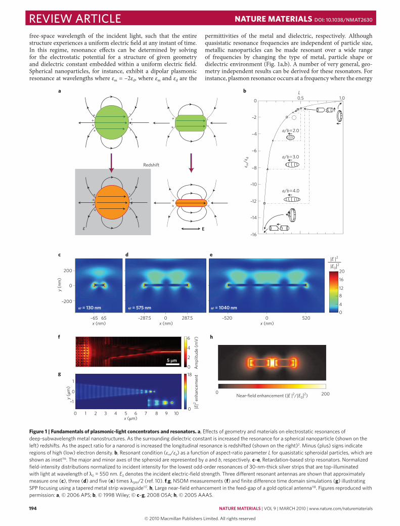
freespace wavelength of the incident light, such that the entire structure experiences a uniform electric field at any instant of time. In this regime, resonance effects can be determined by solving for the electrostatic potential for a structure of given geometry and dielectric constant embedded within a uniform electric field. Spherical nano particles, for instance, exhibit a dipolar plasmonic resonance at wavelengths where εm = –2εd, where εm and εd are the
permittivities of the metal and dielectric, respectively. Although quasistatic resonance frequencies are independent of particle size, metallic nanoparticles can be made resonant over a wide range of frequencies by changing the type of metal, particle shape or dielectric environment (Fig. 1a,b). A number of very general, geometry independent results can be derived for these resonators. For instance, plasmon resonance occurs at a frequency where the energy
++
++
––
––
++
++
––
––
––
––
++
++
Redshift
ε
a b
c|E |2
|E0|2
–16
–14
–12
–10
–8
–6
–4a/b=2.0
a/b=3.0
ε m/ε
d
a/b=4.0
–2
0
L0.5 1.0
d e
200
–200
–65 –287.5 –5200
4
812
16
20
520287.565 0 0
0
y (n
m)
x (nm)
ω = 130 nm ω = 575 nm ω = 1040 nm
x (nm) x (nm)
6
4
2
0
0
18
|E|2 e
nhan
cem
ent
5 µm
f
g
h
0Near-field enhancement (|E |2/|E0|2) 200
0 1
–1
0
1
2 3 4 5x (µm)
y (µ
m)
6 7 8 9 10
E
Am
plitu
de (m
V)
Figure 1 | Fundamentals of plasmonic-light concentrators and resonators. a, Effects of geometry and materials on electrostatic resonances of deep-subwavelength metal nanostructures. As the surrounding dielectric constant is increased the resonance for a spherical nanoparticle (shown on the left) redshifts. As the aspect ratio for a nanorod is increased the longitudinal resonance is redshifted (shown on the right)2. Minus (plus) signs indicate regions of high (low) electron density. b, Resonant condition (εm/εd) as a function of aspect-ratio parameter L for quasistatic spheroidal particles, which are shown as inset116. The major and minor axes of the spheroid are represented by a and b, respectively. c–e, Retardation-based strip resonators. Normalized field-intensity distributions normalized to incident intensity for the lowest odd-order resonances of 30-nm-thick silver strips that are top-illuminated with light at wavelength of λ0 = 550 nm. E0 denotes the incident electric-field strength. Three different resonant antennas are shown that approximately measure one (c), three (d) and five (e) times λSPP/2 (ref. 10). f,g, NSOM measurements (f) and finite difference time domain simulations (g) illustrating SPP focusing using a tapered metal strip waveguide117. h, Large near-field enhancement in the feed-gap of a gold optical antenna118. Figures reproduced with permission: a, © 2006 APS; b, © 1998 Wiley; © c–g, 2008 OSA; h, © 2005 AAAS.
nmat_2630_MAR10.indd 194 9/2/10 11:16:03
© 20 Macmillan Publishers Limited. All rights reserved10
nature materials | VOL 9 | MARCH 2010 | www.nature.com/naturematerials 195
review articleNaTure maTerIals doi: 10.1038/nmat2630
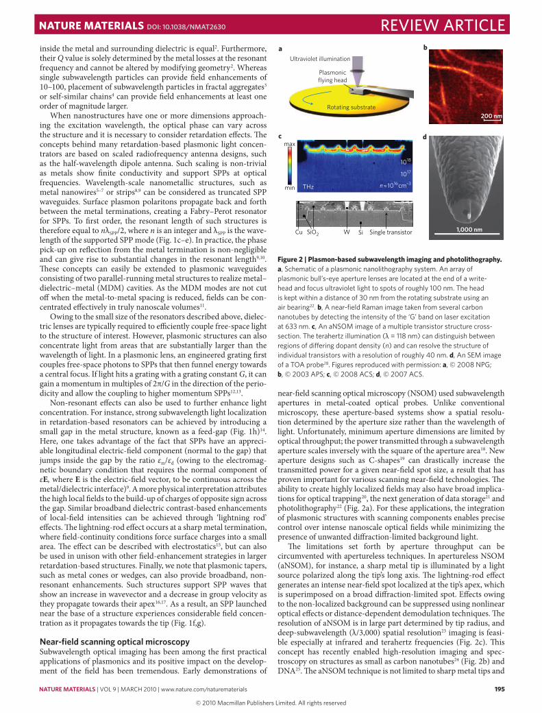
nearfield scanning optical microscopy (NSOM) used subwavelength apertures in metalcoated optical probes. Unlike conventional microscopy, these aperturebased systems show a spatial resolution determined by the aperture size rather than the wavelength of light. Unfortunately, minimum aperture dimensions are limited by optical throughput; the power transmitted through a subwavelength aperture scales inversely with the square of the aperture area18. New aperture designs such as Cshapes19 can drastically increase the transmitted power for a given nearfield spot size, a result that has proven important for various scanning nearfield technologies. The ability to create highly localized fields may also have broad implications for optical trapping20, the next generation of data storage21 and photolithography22 (Fig. 2a). For these applications, the integration of plasmonic structures with scanning components enables precise control over intense nanoscale optical fields while minimizing the presence of unwanted diffractionlimited background light.
The limitations set forth by aperture throughput can be circumvented with apertureless techniques. In apertureless NSOM (aNSOM), for instance, a sharp metal tip is illuminated by a light source polarized along the tip’s long axis. The lightningrod effect generates an intense nearfield spot localized at the tip’s apex, which is superimposed on a broad diffractionlimited spot. Effects owing to the nonlocalized background can be suppressed using nonlinear optical effects or distancedependent demodulation techniques. The resolution of aNSOM is in large part determined by tip radius, and deepsubwavelength (λ/3,000) spatial resolution23 imaging is feasible especially at infrared and terahertz frequencies (Fig. 2c). This concept has recently enabled highresolution imaging and spectroscopy on structures as small as carbon nanotubes24 (Fig. 2b) and DNA25. The aNSOM technique is not limited to sharp metal tips and
Rotating substrate
Plasmonicflying head
Ultraviolet illumination
200 nm
a b
Cu SiO2 W Si Single transistor
min
max
THz
c d
1,000 nm
1018
1017
n≈1016cm–3
inside the metal and surrounding dielectric is equal2. Furthermore, their Q value is solely determined by the metal losses at the resonant frequency and cannot be altered by modifying geometry2. Whereas single subwavelength particles can provide field enhancements of 10–100, placement of subwavelength particles in fractal aggregates3 or selfsimilar chains4 can provide field enhancements at least one order of magnitude larger.
When nanostructures have one or more dimensions approaching the excitation wavelength, the optical phase can vary across the structure and it is necessary to consider retardation effects. The concepts behind many retardationbased plasmonic light concentrators are based on scaled radiofrequency antenna designs, such as the halfwavelength dipole antenna. Such scaling is nontrivial as metals show finite conductivity and support SPPs at optical frequencies. Wavelengthscale nanometallic structures, such as metal nanowires5–7 or strips8,9 can be considered as truncated SPP waveguides. Surface plasmon polaritons propagate back and forth between the metal terminations, creating a Fabry–Perot resonator for SPPs. To first order, the resonant length of such structures is therefore equal to nλSPP/2, where n is an integer and λSPP is the wavelength of the supported SPP mode (Fig. 1c–e). In practice, the phase pickup on reflection from the metal termination is nonnegligible and can give rise to substantial changes in the resonant length9,10.
These concepts can easily be extended to plasmonic waveguides consisting of two parallelrunning metal structures to realize metal–dielectric–metal (MDM) cavities. As the MDM modes are not cut off when the metaltometal spacing is reduced, fields can be concentrated effectively in truly nanoscale volumes11.
Owing to the small size of the resonators described above, dielectric lenses are typically required to efficiently couple freespace light to the structure of interest. However, plasmonic structures can also concentrate light from areas that are substantially larger than the wavelength of light. In a plasmonic lens, an engineered grating first couples freespace photons to SPPs that then funnel energy towards a central focus. If light hits a grating with a grating constant G, it can gain a momentum in multiples of 2π/G in the direction of the periodicity and allow the coupling to higher momentum SPPs12,13.
Nonresonant effects can also be used to further enhance light concentration. For instance, strong subwavelength light localization in retardationbased resonators can be achieved by introducing a small gap in the metal structure, known as a feedgap (Fig. 1h)14. Here, one takes advantage of the fact that SPPs have an appreciable longitudinal electricfield component (normal to the gap) that jumps inside the gap by the ratio εm/εd (owing to the electromagnetic boundary condition that requires the normal component of εE, where E is the electricfield vector, to be continuous across the metal/dielectric interface)9. A more physical interpretation attributes the high local fields to the buildup of charges of opposite sign across the gap. Similar broadband dielectric contrastbased enhancements of localfield intensities can be achieved through ‘lightning rod’ effects. The lightningrod effect occurs at a sharp metal termination, where fieldcontinuity conditions force surface charges into a small area. The effect can be described with electrostatics15, but can also be used in unison with other fieldenhancement strategies in larger retardationbased structures. Finally, we note that plasmonic tapers, such as metal cones or wedges, can also provide broadband, nonresonant enhancements. Such structures support SPP waves that show an increase in wavevector and a decrease in group velocity as they propagate towards their apex16,17. As a result, an SPP launched near the base of a structure experiences considerable field concentration as it propagates towards the tip (Fig. 1f,g).
near-field scanning optical microscopySubwavelength optical imaging has been among the first practical applications of plasmonics and its positive impact on the development of the field has been tremendous. Early demonstrations of
Figure 2 | Plasmon-based subwavelength imaging and photolithography. a, Schematic of a plasmonic nanolithography system. An array of plasmonic bull’s-eye aperture lenses are located at the end of a write-head and focus ultraviolet light to spots of roughly 100 nm. The head is kept within a distance of 30 nm from the rotating substrate using an air bearing22. b, A near-field Raman image taken from several carbon nanotubes by detecting the intensity of the ‘G’ band on laser excitation at 633 nm. c, An aNSOM image of a multiple transistor structure cross-section. The terahertz illumination (λ = 118 nm) can distinguish between regions of differing dopant density (n) and can resolve the structure of individual transistors with a resolution of roughly 40 nm. d, An SEM image of a TOA probe28. Figures reproduced with permission: a, © 2008 NPG; b, © 2003 APS; c, © 2008 ACS; d, © 2007 ACS.
nmat_2630_MAR10.indd 195 9/2/10 11:16:04
© 20 Macmillan Publishers Limited. All rights reserved10
196 nature materials | VOL 9 | MARCH 2010 | www.nature.com/naturematerials
review article NaTure maTerIals doi: 10.1038/nmat2630
alternative configurations have used different lightconcentrating structures including metal nanoparticles26 and bowtie antennas27.
The tiponaperture (TOA) approach is a particularly interesting probe geometry that has emerged recently. Here, a metal protrusion is deposited adjacent to an NSOM aperture, further localizing the aperture fields. Tiponaperture combines the background suppression of conventional apertures with the enhanced fields and tiplimited resolution of apertureless techniques. Initial TOA techniques achieved field enhancements owing to tip sharpness only25. Later, researchers optimized tip length to fully take advantage of retardation effects28 (Fig. 2d). Although primarily used in nearfield microscopy, the TOA method could prove useful for a diversity of technologies that require light to be delivered to extremely small volumes.
PhotodetectorsThe ability of plasmonic structures to manipulate light well below the classical diffraction limit is giving rise to a myriad of new chipscale photonic components. The integration of plasmonic structures with existing electronic and dielectric devices can be realized by an increasing number of nanofabrication techniques, including mature siliconintegratedcircuit technology. Of the many emerging applications, plasmonenhanced photodetectors are particularly promising.
At present, our ability to shrink conventional photodetectors is constrained in the lateral dimensions by the diffraction limit and in the vertical dimension by the finite absorption depth of semiconductors. These size limitations significantly affect detector performance. Reducing detector size below these limits would result in increased speed, decreased noise and reduced power consumption. The speed of a detector is generally limited either by its carriertransit time (the time it takes photogenerated carriers to transit the detector’s intrinsic region), or resistor–capacitor (RC) time constant (the time required to charge the device’s effective capacitance, C). Whereas the carriertransit time scales with the length of the device,
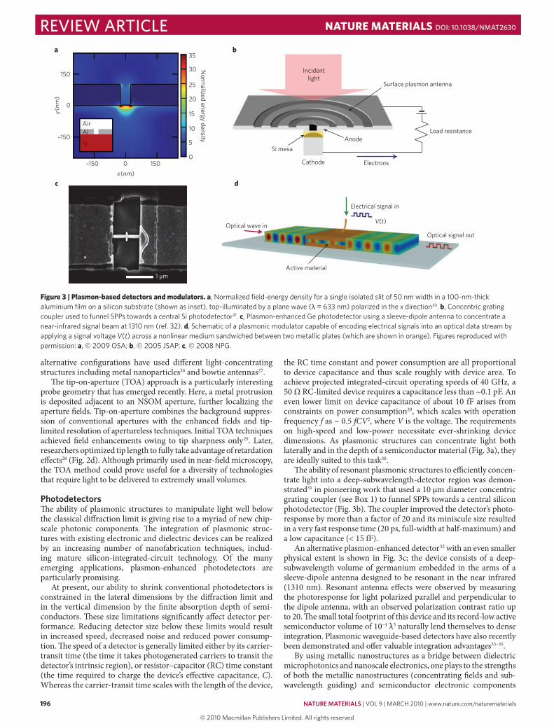
the RC time constant and power consumption are all proportional to device capacitance and thus scale roughly with device area. To achieve projected integratedcircuit operating speeds of 40 GHz, a 50 Ω RClimited device requires a capacitance less than ~0.1 pF. An even lower limit on device capacitance of about 10 fF arises from constraints on power consumption29, which scales with operation frequency f as ~ 0.5 fCV2, where V is the voltage. The requirements on highspeed and lowpower necessitate evershrinking device dimensions. As plasmonic structures can concentrate light both laterally and in the depth of a semiconductor material (Fig. 3a), they are ideally suited to this task30.
The ability of resonant plasmonic structures to efficiently concentrate light into a deepsubwavelengthdetector region was demonstrated31 in pioneering work that used a 10 μm diameter concentric grating coupler (see Box 1) to funnel SPPs towards a central silicon photodetector (Fig. 3b). The coupler improved the detector’s photoresponse by more than a factor of 20 and its miniscule size resulted in a very fast response time (20 ps, fullwidth at halfmaximum) and a low capacitance (< 15 fF).
An alternative plasmonenhanced detector32 with an even smaller physical extent is shown in Fig. 3c; the device consists of a deepsubwavelength volume of germanium embedded in the arms of a sleevedipole antenna designed to be resonant in the near infrared (1310 nm). Resonant antenna effects were observed by measuring the photoresponse for light polarized parallel and perpendicular to the dipole antenna, with an observed polarization contrast ratio up to 20. The small total footprint of this device and its recordlow active semiconductor volume of 10–4 λ3 naturally lend themselves to dense integration. Plasmonic waveguidebased detectors have also recently been demonstrated and offer valuable integration advantages33–35.
By using metallic nanostructures as a bridge between dielectric microphotonics and nanoscale electronics, one plays to the strengths of both the metallic nanostructures (concentrating fields and subwavelength guiding) and semiconductor electronic components
AirAI
Si
x(nm)
150
a b
c
150
–150
–150
0
00
5
10
15
20
25
30
35y(
nm)
d
1 µm
Incidentlight
Surface plasmon antenna
Load resistanceAnode
ElectronsCathode
Si mesa
V(t)
Active material
Optical wave in
Electrical signal in
Optical signal out
Norm
alized energy density
Figure 3 | Plasmon-based detectors and modulators. a, Normalized field-energy density for a single isolated slit of 50 nm width in a 100-nm-thick aluminium film on a silicon substrate (shown as inset), top-illuminated by a plane wave (λ = 633 nm) polarized in the x direction30. b, Concentric grating coupler used to funnel SPPs towards a central Si photodetector31. c, Plasmon-enhanced Ge photodetector using a sleeve-dipole antenna to concentrate a near-infrared signal beam at 1310 nm (ref. 32). d, Schematic of a plasmonic modulator capable of encoding electrical signals into an optical data stream by applying a signal voltage V(t) across a nonlinear medium sandwiched between two metallic plates (which are shown in orange). Figures reproduced with permission: a, © 2009 OSA; b, © 2005 JSAP; c, © 2008 NPG.
nmat_2630_MAR10.indd 196 9/2/10 11:16:06
© 20 Macmillan Publishers Limited. All rights reserved10
nature materials | VOL 9 | MARCH 2010 | www.nature.com/naturematerials 197
review articleNaTure maTerIals doi: 10.1038/nmat2630
(highspeed and highperformance information processing). Plasmonics also offers the possibility of introducing new functionality, including polarization, angle or wavelength selectivity36.
modulatorsAs well as photodetectors, the realization of a complete chipscale optical link will require highspeed and powerefficient optical
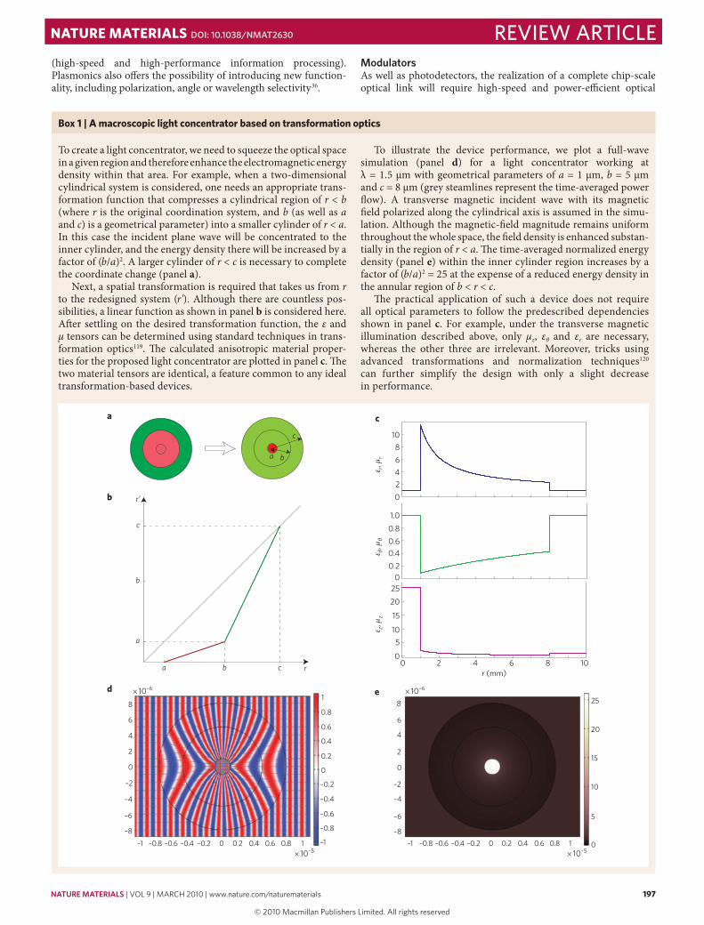
To create a light concentrator, we need to squeeze the optical space in a given region and therefore enhance the electro magnetic energy density within that area. For example, when a twodimensional cylindrical system is considered, one needs an appropriate transformation function that compresses a cylindrical region of r < b (where r is the original coordination system, and b (as well as a and c) is a geometrical parameter) into a smaller cylinder of r < a. In this case the incident plane wave will be concentrated to the inner cylinder, and the energy density there will be increased by a factor of (b/a)2. A larger cylinder of r < c is necessary to complete the coordinate change (panel a).
Next, a spatial transformation is required that takes us from r to the redesigned system (r'). Although there are countless possibilities, a linear function as shown in panel b is considered here. After settling on the desired transformation function, the ε and μ tensors can be determined using standard techniques in transformation optics119. The calculated anisotropic material properties for the proposed light concentrator are plotted in panel c. The two material tensors are identical, a feature common to any ideal transformationbased devices.
To illustrate the device performance, we plot a fullwave simulation (panel d) for a light concentrator working at λ = 1.5 μm with geometrical parameters of a = 1 μm, b = 5 μm and c = 8 μm (grey steamlines represent the timeaveraged power flow). A transverse magnetic incident wave with its magnetic field polarized along the cylindrical axis is assumed in the simulation. Although the magneticfield magnitude remains uniform throughout the whole space, the field density is enhanced substantially in the region of r < a. The timeaveraged normalized energy density (panel e) within the inner cylinder region increases by a factor of (b/a)2 = 25 at the expense of a reduced energy density in the annular region of b < r < c.
The practical application of such a device does not require all optical parameters to follow the predescribed dependencies shown in panel c. For example, under the transverse magnetic illumination described above, only μz, εθ and εr are necessary, whereas the other three are irrelevant. Moreover, tricks using advanced transformations and normalization techniques120 can further simplify the design with only a slight decrease in performance.
Box 1 | a macroscopic light concentrator based on transformation optics
a b c
a
b
c
r
r’ 02468
10
0
510
15
2025
0 2 4 6 8 10r (mm)
a
b
c
d
1.00.80.60.40.2
0
e
–1 –0.8 –0.6 –0.4 –0.2 0.2 0.4 0.6 0.8 10 –1 –0.8 –0.6 –0.4 –0.2 0.2 0.4 0.6 0.8 10
× 10–6
× 10–5 × 10–5
× 10–6
–8
–6
–4
–2
0
4
2
6
8
–0.8
–1
–0.6
–0.4
–0.2
0
0
5
10
15
20
25
0.2
0.4
0.6
0.8
1
a b
c
–8
–6
–4
–2
0
2
4
6
8
ε r, µ
rε z
, µz
ε θ, µ
θ
nmat_2630_MAR10.indd 197 9/2/10 11:16:06
© 20 Macmillan Publishers Limited. All rights reserved10
198 nature materials | VOL 9 | MARCH 2010 | www.nature.com/naturematerials
review article NaTure maTerIals doi: 10.1038/nmat2630
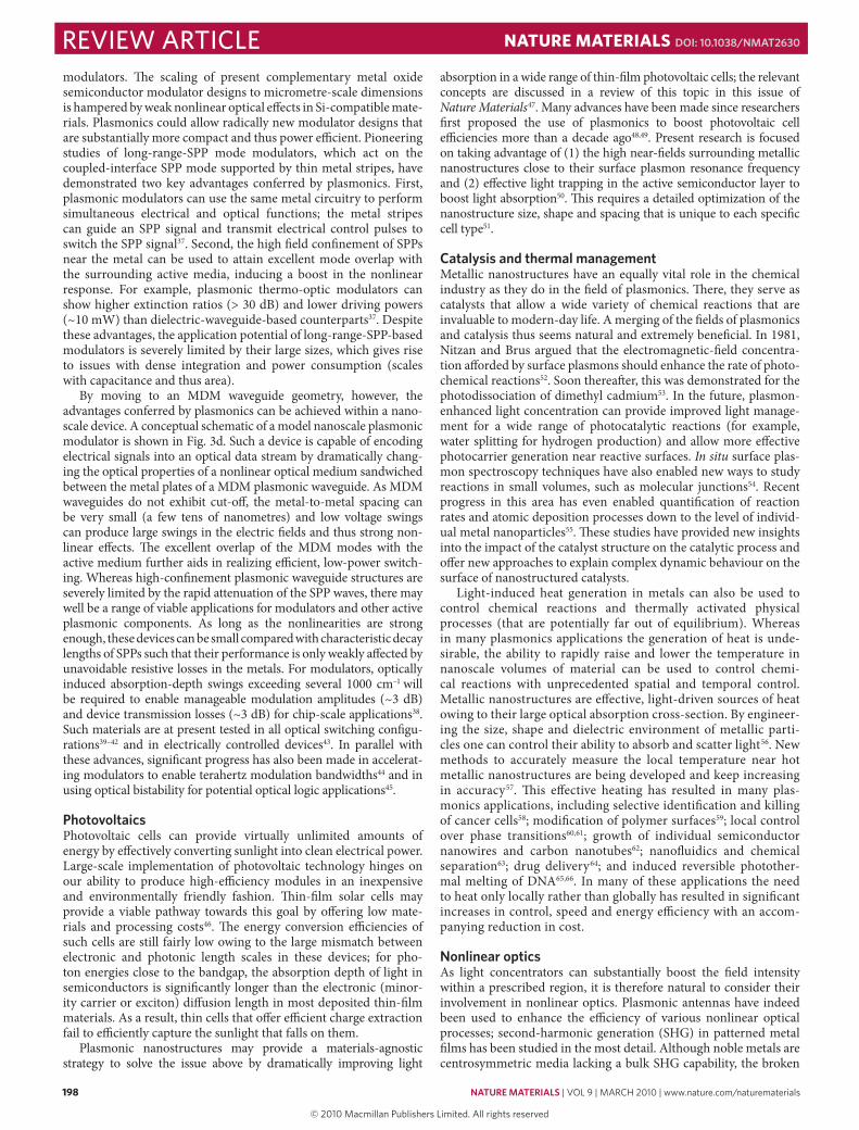
modulators. The scaling of present complementary metal oxide semiconductor modulator designs to micrometrescale dimensions is hampered by weak nonlinear optical effects in Sicompatible materials. Plasmonics could allow radically new modulator designs that are substantially more compact and thus power efficient. Pioneering studies of longrangeSPP mode modulators, which act on the coupledinterface SPP mode supported by thin metal stripes, have demonstrated two key advantages conferred by plasmonics. First, plasmonic modulators can use the same metal circuitry to perform simultaneous electrical and optical functions; the metal stripes can guide an SPP signal and transmit electrical control pulses to switch the SPP signal37. Second, the high field confinement of SPPs near the metal can be used to attain excellent mode overlap with the surrounding active media, inducing a boost in the nonlinear response. For example, plasmonic thermooptic modulators can show higher extinction ratios (> 30 dB) and lower driving powers (~10 mW) than dielectricwaveguidebased counterparts37. Despite these advantages, the application potential of longrangeSPPbased modulators is severely limited by their large sizes, which gives rise to issues with dense integration and power consumption (scales with capacitance and thus area).
By moving to an MDM waveguide geometry, however, the advantages conferred by plasmonics can be achieved within a nanoscale device. A conceptual schematic of a model nanoscale plasmonic modulator is shown in Fig. 3d. Such a device is capable of encoding electrical signals into an optical data stream by dramatically changing the optical properties of a nonlinear optical medium sandwiched between the metal plates of a MDM plasmonic waveguide. As MDM waveguides do not exhibit cutoff, the metaltometal spacing can be very small (a few tens of nanometres) and low voltage swings can produce large swings in the electric fields and thus strong nonlinear effects. The excellent overlap of the MDM modes with the active medium further aids in realizing efficient, lowpower switching. Whereas highconfinement plasmonic waveguide structures are severely limited by the rapid attenuation of the SPP waves, there may well be a range of viable applications for modulators and other active plasmonic components. As long as the nonlinearities are strong enough, these devices can be small compared with characteristic decay lengths of SPPs such that their performance is only weakly affected by unavoidable resistive losses in the metals. For modulators, optically induced absorptiondepth swings exceeding several 1000 cm–1
will be required to enable manageable modulation amplitudes (~3 dB) and device transmission losses (~3 dB) for chipscale applications38. Such materials are at present tested in all optical switching configurations39–42 and in electrically controlled devices43. In parallel with these advances, significant progress has also been made in accelerating modulators to enable terahertz modulation bandwidths44 and in using optical bistability for potential optical logic applications45.
PhotovoltaicsPhotovoltaic cells can provide virtually unlimited amounts of energy by effectively converting sunlight into clean electrical power. Largescale implementation of photovoltaic technology hinges on our ability to produce highefficiency modules in an inexpensive and environmentally friendly fashion. Thinfilm solar cells may provide a viable pathway towards this goal by offering low materials and processing costs46. The energy conversion efficiencies of such cells are still fairly low owing to the large mismatch between electronic and photonic length scales in these devices; for photon energies close to the bandgap, the absorption depth of light in semiconductors is significantly longer than the electronic (minority carrier or exciton) diffusion length in most deposited thinfilm materials. As a result, thin cells that offer efficient charge extraction fail to efficiently capture the sunlight that falls on them.
Plasmonic nanostructures may provide a materialsagnostic strategy to solve the issue above by dramatically improving light
absorption in a wide range of thinfilm photovoltaic cells; the relevant concepts are discussed in a review of this topic in this issue of Nature Materials47. Many advances have been made since researchers first proposed the use of plasmonics to boost photovoltaic cell efficiencies more than a decade ago48,49. Present research is focused on taking advantage of (1) the high nearfields surrounding metallic nanostructures close to their surface plasmon resonance frequency and (2) effective light trapping in the active semiconductor layer to boost light absorption50. This requires a detailed optimization of the nanostructure size, shape and spacing that is unique to each specific cell type51.
Catalysis and thermal managementMetallic nanostructures have an equally vital role in the chemical industry as they do in the field of plasmonics. There, they serve as catalysts that allow a wide variety of chemical reactions that are invaluable to modernday life. A merging of the fields of plasmonics and catalysis thus seems natural and extremely beneficial. In 1981, Nitzan and Brus argued that the electromagneticfield concentration afforded by surface plasmons should enhance the rate of photochemical reactions52. Soon thereafter, this was demonstrated for the photodissociation of dimethyl cadmium53. In the future, plasmonenhanced light concentration can provide improved light management for a wide range of photocatalytic reactions (for example, water splitting for hydrogen production) and allow more effective photocarrier generation near reactive surfaces. In situ surface plasmon spectroscopy techniques have also enabled new ways to study reactions in small volumes, such as molecular junctions54. Recent progress in this area has even enabled quantification of reaction rates and atomic deposition processes down to the level of individual metal nanoparticles55. These studies have provided new insights into the impact of the catalyst structure on the catalytic process and offer new approaches to explain complex dynamic behaviour on the surface of nanostructured catalysts.
Lightinduced heat generation in metals can also be used to control chemical reactions and thermally activated physical processes (that are potentially far out of equilibrium). Whereas in many plasmonics applications the generation of heat is undesirable, the ability to rapidly raise and lower the temperature in nanoscale volumes of material can be used to control chemical reactions with unprecedented spatial and temporal control. Metallic nanostructures are effective, lightdriven sources of heat owing to their large optical absorption crosssection. By engineering the size, shape and dielectric environment of metallic particles one can control their ability to absorb and scatter light56. New methods to accurately measure the local temperature near hot metallic nanostructures are being developed and keep increasing in accuracy57. This effective heating has resulted in many plasmonics applications, including selective identification and killing of cancer cells58; modification of polymer surfaces59; local control over phase transitions60,61; growth of individual semiconductor nanowires and carbon nanotubes62; nanofluidics and chemical separation63; drug delivery64; and induced reversible photothermal melting of DNA65,66. In many of these applications the need to heat only locally rather than globally has resulted in significant increases in control, speed and energy efficiency with an accompanying reduction in cost.
nonlinear opticsAs light concentrators can substantially boost the field intensity within a prescribed region, it is therefore natural to consider their involvement in nonlinear optics. Plasmonic antennas have indeed been used to enhance the efficiency of various nonlinear optical processes; secondharmonic generation (SHG) in patterned metal films has been studied in the most detail. Although noble metals are centrosymmetric media lacking a bulk SHG capability, the broken
nmat_2630_MAR10.indd 198 9/2/10 11:16:07
© 20 Macmillan Publishers Limited. All rights reserved10
nature materials | VOL 9 | MARCH 2010 | www.nature.com/naturematerials 199
review articleNaTure maTerIals doi: 10.1038/nmat2630
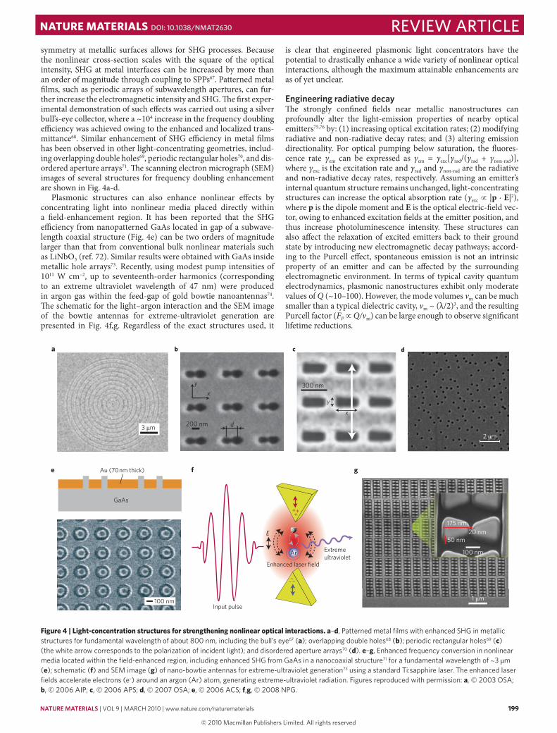
symmetry at metallic surfaces allows for SHG processes. Because the nonlinear crosssection scales with the square of the optical intensity, SHG at metal interfaces can be increased by more than an order of magnitude through coupling to SPPs67. Patterned metal films, such as periodic arrays of subwavelength apertures, can further increase the electromagnetic intensity and SHG. The first experimental demonstration of such effects was carried out using a silver bull’seye collector, where a ~104 increase in the frequency doubling efficiency was achieved owing to the enhanced and localized transmittance68. Similar enhancement of SHG efficiency in metal films has been observed in other lightconcentrating geometries, including overlapping double holes69, periodic rectangular holes70, and disordered aperture arrays71. The scanning electron micrograph (SEM) images of several structures for frequency doubling enhancement are shown in Fig. 4ad.
Plasmonic structures can also enhance nonlinear effects by concentrating light into nonlinear media placed directly within a fieldenhancement region. It has been reported that the SHG efficiency from nanopatterned GaAs located in gap of a subwavelength coaxial structure (Fig. 4e) can be two orders of magnitude larger than that from conventional bulk nonlinear materials such as LiNbO3 (ref. 72). Similar results were obtained with GaAs inside metallic hole arrays73. Recently, using modest pump intensities of 1011 W cm–2, up to seventeenthorder harmonics (corresponding to an extreme ultraviolet wavelength of 47 nm) were produced in argon gas within the feedgap of gold bowtie nano antennas74. The schematic for the light–argon interaction and the SEM image of the bowtie antennas for extremeultraviolet generation are presented in Fig. 4f,g. Regardless of the exact structures used, it
is clear that engineered plasmonic light concentrators have the potential to drastically enhance a wide variety of nonlinear optical interactions, although the maximum attainable enhancements are as of yet unclear.
engineering radiative decayThe strongly confined fields near metallic nanostructures can profoundly alter the lightemission properties of nearby optical emitters75,76 by: (1) increasing optical excitation rates; (2) modifying radiative and nonradiative decay rates; and (3) altering emission directionality. For optical pumping below saturation, the fluorescence rate γem can be expressed as γem = γexc[γrad/(γrad + γnonrad)], where γexc is the excitation rate and γrad and γnonrad are the radiative and nonradiative decay rates, respectively. Assuming an emitter’s internal quantum structure remains unchanged, lightconcentrating structures can increase the optical absorption rate (γexc ∝ |p · E|2), where p is the dipole moment and E is the optical electricfield vector, owing to enhanced excitation fields at the emitter position, and thus increase photoluminescence intensity. These structures can also affect the relaxation of excited emitters back to their ground state by introducing new electromagnetic decay pathways; according to the Purcell effect, spontaneous emission is not an intrinsic property of an emitter and can be affected by the surrounding electromagnetic environment. In terms of typical cavity quantum electrodynamics, plasmonic nanostructures exhibit only moderate values of Q (~10–100). However, the mode volumes vm can be much smaller than a typical dielectric cavity, vm ~ (λ/2)3, and the resulting Purcell factor (FP ∝ Q/vm) can be large enough to observe significant lifetime reductions.
e–
Ar
e f g
dcba
x
y
Au (70nm thick)
Extremeultraviolet
E
Enhanced laser field
Input pulse
2 µm
200 nm d
xy 300 nm
3 µm
GaAs
100 nm
100 nm
1 µm
20 nm175 nm
50 nm
+++
–––
Figure 4 | light-concentration structures for strengthening nonlinear optical interactions. a–d, Patterned metal films with enhanced SHG in metallic structures for fundamental wavelength of about 800 nm, including the bull’s eye67 (a); overlapping double holes68 (b); periodic rectangular holes69 (c) (the white arrow corresponds to the polarization of incident light); and disordered aperture arrays70 (d). e–g, Enhanced frequency conversion in nonlinear media located within the field-enhanced region, including enhanced SHG from GaAs in a nanocoaxial structure71 for a fundamental wavelength of ~3 µm (e); schematic (f) and SEM image (g) of nano-bowtie antennas for extreme-ultraviolet generation73 using a standard Ti:sapphire laser. The enhanced laser fields accelerate electrons (e–) around an argon (Ar) atom, generating extreme-ultraviolet radiation. Figures reproduced with permission: a, © 2003 OSA; b, © 2006 AIP; c, © 2006 APS; d, © 2007 OSA; e, © 2006 ACS; f,g, © 2008 NPG.
nmat_2630_MAR10.indd 199 9/2/10 11:16:08
© 20 Macmillan Publishers Limited. All rights reserved10

200 nature materials | VOL 9 | MARCH 2010 | www.nature.com/naturematerials
review article NaTure maTerIals doi: 10.1038/nmat2630
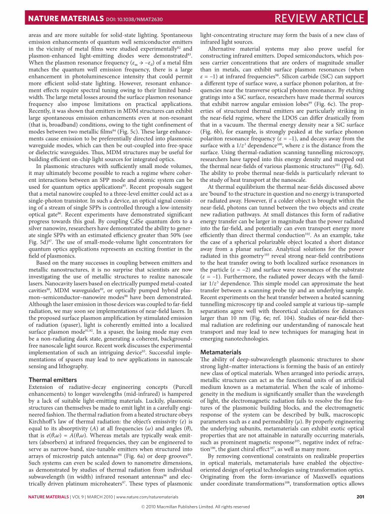
When located near metal nanoparticles, excited molecules relax rapidly by exciting localized surface plasmons by means of nearfield coupling. The total decay rate (γ rad + γnonrad) can increase by a considerable degree owing to the large local density of optical states (LDOS) near the metal surface. Particularly large enhancements are obtained when the molecular emission frequency matches the surface plasmon resonance frequency of the nanoparticle or if fields are squeezed into a smaller volume by coupling to a second nanoparticle77. Once excited, localized surface plasmons can either decay nonradiatively because of internal damping, or reradiate into free space. Depending on a variety of parameters, coupled molecule–nanoparticle systems can exhibit either increased or decreased (quenching) luminescence75,76,78, as shown in Fig. 5a. For most applications it is desirable that metal nanoparticles behave in a similar way to optical antennas — increasing luminescence yields by obtaining energy from nearby emitters and redistributing it to the farfield. Recently, it was also demonstrated that the angular emission of a single molecule near a metal nanoparticle (that is, optical antenna)
follows the antenna mode, regardless of the molecular orientation79. Thus, properly designed metal nanoparticles can both increase light output and redirect light emission into preferred directions, resulting in a superior class of light emitter.
Subwavelength metal holes can also enhance excitation and decay rates of embedded emitters by means of coupling to guided SPP modes. Depending on the hole diameter, these two effects may have varying contribution to the total fluorescence enhancement80 (Fig. 5b). The observed enhancement is largest around the cutoff of the fundamental guided mode of the excitation field, where the group velocity is minimized and the LDOS is maximized. By using nanoholes to restrict excitation and collection to a nanoscale volume, researchers can now perform fluorescencebased singlemolecule detection at high, micromolar concentrations81.
Localized surface plasmons in metal nanoparticles and holes couple to only a small number of nearby emitters and are useful for singlemolecule spectroscopy. Propagating SPPs on metal films, on the other hand, can affect light emission over large
z (nm)
z
80 nm Au
0 20 40 600
10
20
30
0
2
4
6
8Co
unt r
ate
(kH
z)
a
c
12
10
8
6
4
2300250200150100
Aperture diameter (nm)
L = 30 nm
L = 50 nm
L = 100 nm
4000
20
40
60
80
100
800 1,200 1,600
Wavelength (nm)
F p
Heat
Gold 200 nm
80–310nmGlass
ExcitationFluorescence
ηF, sat
ηF, low
oγem
γem
Γrad
Γpl
b
d
Enha
ncem
ent t
o op
en s
olut
ion
Figure 5 | radiative-decay engineering and quantum plasmonics. a, Fluorescence rate (γem) of a vertically oriented molecule near a metal nanoparticle as a function of particle–surface distance (z) normalized by the rate in the absence of the nanoparticle (γ0
em). The fluorescence enhancement reaches a maximum at a distance of z ≈ 5 nm. For shorter distances, fluorescence is quenched (red curve: theory; black dots: experiment)74. b, Fluorescence enhancement of a single molecule in a metal nanohole as a function of hole diameter (red curve: at fluorescence saturation (ηF, sat); blue curve: below saturation (ηF, low)). Error bars indicate the standard deviation of measurements and numerical fitting. The enhancement difference between the red and blue curves results from the respective influence of the excitation intensity enhancement and lifetime reduction79. c, Spontaneous emission enhancement of a dipole source in an MDM slab as a function of emission wavelength. The dipole source is in the centre of the gap and oscillates normal to the interfaces. As the gap size L (shown as inset) decreases, the enhancement factor (FP) increases rapidly83. d, Generation of guided single plasmons (shown in red) along a silver nanowire86. Γrad and Γpl refer to the spontaneous emission rate of a coupled quantum dot into free space or guided surface plasmons, respectively. Figures reproduced with permission: a, © 2006 APS; b, © 2008 OSA; c, © 2008 APS; d, © 2007 NPG.
nmat_2630_MAR10.indd 200 9/2/10 11:16:09
© 20 Macmillan Publishers Limited. All rights reserved10
nature materials | VOL 9 | MARCH 2010 | www.nature.com/naturematerials 201
review articleNaTure maTerIals doi: 10.1038/nmat2630
areas and are more suitable for solidstate lighting. Spontaneous emission enhancements of quantum well semiconductor emitters in the vicinity of metal films were studied experimentally82 and plasmonenhanced lightemitting diodes were demonstrated83. When the plasmon resonance frequency (εm → –εd) of a metal film matches the quantum well emission frequency, there is a large enhancement in photoluminescence intensity that could permit more efficient solidstate lighting. However, resonant enhancement effects require spectral tuning owing to their limited bandwidth. The large metal losses around the surface plasmon resonance frequency also impose limitations on practical applications. Recently, it was shown that emitters in MDM structures can exhibit large spontaneous emission enhancements even at nonresonant (that is, broadband) conditions, owing to the tight confinement of modes between two metallic films84 (Fig. 5c). These large enhancements cause emission to be preferentially directed into plasmonic waveguide modes, which can then be outcoupled into freespace or dielectric waveguides. Thus, MDM structures may be useful for building efficient onchip light sources for integrated optics.
In plasmonic structures with sufficiently small mode volumes, it may ultimately become possible to reach a regime where coherent interactions between an SPP mode and atomic system can be used for quantum optics applications85. Recent proposals suggest that a metal nanowire coupled to a threelevel emitter could act as a singlephoton transistor. In such a device, an optical signal consisting of a stream of single SPPs is controlled through a lowintensity optical gate86. Recent experiments have demonstrated significant progress towards this goal. By coupling CdSe quantum dots to a silver nanowire, researchers have demonstrated the ability to generate single SPPs with an estimated efficiency greater than 50% (see Fig. 5d)87. The use of smallmodevolume light concentrators for quantum optics applications represents an exciting frontier in the field of plasmonics.
Based on the many successes in coupling between emitters and metallic nanostructures, it is no surprise that scientists are now investigating the use of metallic structures to realize nanoscale lasers. Nanocavity lasers based on electrically pumped metalcoated cavities88, MDM waveguides89, or optically pumped hybrid plasmon–semiconductor–nanowire modes90 have been demonstrated. Although the laser emission in those devices was coupled to farfield radiation, we may soon see implementations of nearfield lasers. In the proposed surface plasmon amplification by stimulated emission of radiation (spaser), light is coherently emitted into a localized surface plasmon mode91,92. In a spaser, the lasing mode may even be a nonradiating dark state, generating a coherent, backgroundfree nanoscale light source. Recent work discusses the experimental implementation of such an intriguing device93. Successful implementations of spasers may lead to new applications in nanoscale sensing and lithography.
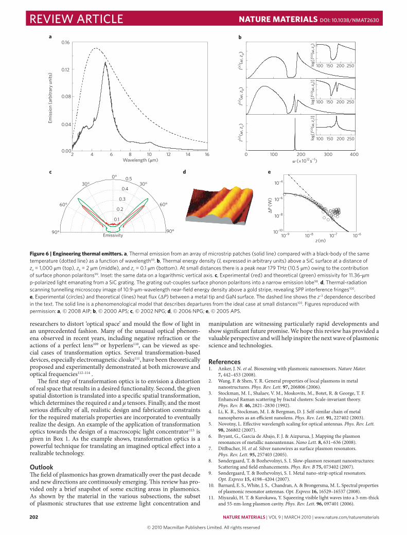
thermal emittersExtension of radiativedecay engineering concepts (Purcell enhancements) to longer wavelengths (midinfrared) is hampered by a lack of suitable lightemitting materials. Luckily, plasmonic structures can themselves be made to emit light in a carefully engineered fashion. The thermal radiation from a heated structure obeys Kirchhoff ’s law of thermal radiation: the object’s emissivity (e) is equal to its absorptivity (A) at all frequencies (ω) and angles (θ), that is e(θ,ω) = A(θ,ω). Whereas metals are typically weak emitters (absorbers) at infrared frequencies, they can be engineered to serve as narrowband, sizetunable emitters when structured into arrays of microstrip patch antennas94 (Fig. 6a) or deep grooves95. Such systems can even be scaled down to nanometre dimensions, as demonstrated by studies of thermal radiation from individual subwavelength (in width) infrared resonant antennas96 and electrically driven platinum microheaters97. These types of plasmonic
lightconcentrating structure may form the basis of a new class of infrared light sources.
Alternative material systems may also prove useful for constructing infrared emitters. Doped semiconductors, which possess carrier concentrations that are orders of magnitude smaller than in metals, can exhibit surface plasmon resonances (when ε = –1) at infrared frequencies98. Silicon carbide (SiC) can support a different type of surface wave, a surface phonon polariton, at frequencies near the transverse optical phonon resonance. By etching gratings into a SiC surface, researchers have made thermal sources that exhibit narrow angular emission lobes99 (Fig. 6c). The properties of structured thermal emitters are particularly striking in the nearfield regime, where the LDOS can differ drastically from that in a vacuum. The thermal energy density near a SiC surface (Fig. 6b), for example, is strongly peaked at the surface phonon polariton resonance frequency (ε = –1), and decays away from the surface with a 1/z3 dependence100, where z is the distance from the surface. Using thermalradiation scanning tunnelling microscopy, researchers have tapped into this energy density and mapped out the thermal nearfields of various plasmonic structures101 (Fig. 6d). The ability to probe thermal nearfields is particularly relevant to the study of heat transport at the nanoscale.
At thermal equilibrium the thermal nearfields discussed above are ‘bound’ to the structure in question and no energy is transported or radiated away. However, if a colder object is brought within the nearfield, photons can tunnel between the two objects and create new radiation pathways. At small distances this form of radiative energy transfer can be larger in magnitude than the power radiated into the farfield, and potentially can even transport energy more efficiently than direct thermal conduction102. As an example, take the case of a spherical polarizable object located a short distance away from a planar surface. Analytical solutions for the power radiated in this geometry103 reveal strong nearfield contributions to the heat transfer owing to both localized surface resonances in the particle (ε = –2) and surface wave resonances of the substrate (ε = –1). Furthermore, the radiated power decays with the familiar 1/z3 dependence. This simple model can approximate the heat transfer between a scanning probe tip and an underlying sample. Recent experiments on the heat transfer between a heated scanning tunnelling microscopy tip and cooled sample at various tip–sample separations agree well with theoretical calculations for distances larger than 10 nm (Fig. 6e; ref. 104). Studies of nearfield thermal radiation are redefining our understanding of nanoscale heat transport and may lead to new techniques for managing heat in emerging nanotechnologies.
metamaterialsThe ability of deepsubwavelength plasmonic structures to show strong light–matter interactions is forming the basis of an entirely new class of optical materials. When arranged into periodic arrays, metallic structures can act as the functional units of an artificial medium known as a metamaterial. When the scale of inhomogeneity in the medium is significantly smaller than the wavelength of light, the electromagnetic radiation fails to resolve the fine features of the plasmonic building blocks, and the electromagnetic response of the system can be described by bulk, macroscopic parameters such as ε and permeability (μ). By properly engineering the underlying subunits, metamaterials can exhibit exotic optical properties that are not attainable in naturally occurring materials, such as prominent magnetic response105, negative index of refraction106, the giant chiral effect107, as well as many more.
By removing conventional constraints on realizable properties in optical materials, metamaterials have enabled the objectiveoriented design of optical technologies using transformation optics. Originating from the forminvariance of Maxwell’s equations under coordinate transformations108, transformation optics allows
nmat_2630_MAR10.indd 201 9/2/10 11:16:09
© 20 Macmillan Publishers Limited. All rights reserved10
202 nature materials | VOL 9 | MARCH 2010 | www.nature.com/naturematerials
review article NaTure maTerIals doi: 10.1038/nmat2630
researchers to distort ‘optical space’ and mould the flow of light in an unprecedented fashion. Many of the unusual optical phenomena observed in recent years, including negative refraction or the actions of a perfect lens109 or hyperlens110, can be viewed as special cases of transformation optics. Several transformationbased devices, especially electromagnetic cloaks111, have been theoretically proposed and experimentally demonstrated at both microwave and optical frequencies112–114 .
The first step of transformation optics is to envision a distortion of real space that results in a desired functionality. Second, the given spatial distortion is translated into a specific spatial transformation, which determines the required ε and μ tensors. Finally, and the most serious difficulty of all, realistic design and fabrication constraints for the required materials properties are incorporated to eventually realize the design. An example of the application of transformation optics towards the design of a macroscopic light concentrator115 is given in Box 1. As the example shows, transformation optics is a powerful technique for translating an imagined optical effect into a realizable technology.
outlookThe field of plasmonics has grown dramatically over the past decade and new directions are continuously emerging. This review has provided only a brief snapshot of some exciting areas in plasmonics. As shown by the material in the various subsections, the subset of plasmonic structures that use extreme light concentration and
manipulation are witnessing particularly rapid developments and show significant future promise. We hope this review has provided a valuable perspective and will help inspire the next wave of plasmonic science and technologies.
references1. Anker, J. N. et al. Biosensing with plasmonic nanosensors. Nature Mater.
7, 442–453 (2008).2. Wang, F. & Shen, Y. R. General properties of local plasmons in metal
nanostructures. Phys. Rev. Lett. 97, 206806 (2006).3. Stockman, M. I., Shalaev, V. M., Moskovits, M., Botet, R. & George, T. F.
Enhanced Raman scattering by fractal clusters: Scaleinvariant theory. Phys. Rev. B. 46, 2821–2830 (1992).
4. Li, K. R., Stockman, M. I. & Bergman, D. J. Selfsimilar chain of metal nanospheres as an efficient nanolens. Phys. Rev. Lett. 91, 227402 (2003).
5. Novotny, L. Effective wavelength scaling for optical antennas. Phys. Rev. Lett. 98, 266802 (2007).
6. Bryant, G., Garcia de Abajo, F. J. & Aizpurua, J. Mapping the plasmon resonances of metallic nanoantennas. Nano Lett. 8, 631–636 (2008).
7. Ditlbacher, H. et al. Silver nanowires as surface plasmon resonators. Phys. Rev. Lett. 95, 257403 (2005).
8. Søndergaard, T. & Bozhevolnyi, S. I. Slowplasmon resonant nanostructures: Scattering and field enhancements. Phys. Rev. B 75, 073402 (2007).
9. Søndergaard, T. & Bozhevolnyi, S. I. Metal nanostrip optical resonators. Opt. Express 15, 4198–4204 (2007).
10. Barnard, E. S., White, J. S., Chandran, A. & Brongersma, M. L. Spectral properties of plasmonic resonator antennas. Opt. Express 16, 16529–16537 (2008).
11. Miyazaki, H. T. & Kurokawa, Y. Squeezing visible light waves into a 3nmthick and 55nmlong plasmon cavity. Phys. Rev. Lett. 96, 097401 (2006).
Figure 6 | engineering thermal emitters. a, Thermal emission from an array of microstrip patches (solid line) compared with a black-body of the same temperature (dotted line) as a function of wavelength93. b, Thermal energy density (l, expressed in arbitrary units) above a SiC surface at a distance of za = 1,000 μm (top), zb = 2 μm (middle), and zc = 0.1 μm (bottom). At small distances there is a peak near 179 THz (10.5 μm) owing to the contribution of surface phonon polaritons99. Inset: the same data on a logarithmic vertical axis. c, Experimental (red) and theoretical (green) emissivity for 11.36-μm p-polarized light emanating from a SiC grating. The grating out-couples surface phonon polaritons into a narrow emission lobe98. d, Thermal-radiation scanning tunnelling microscopy image of 10.9-μm-wavelength near-field energy density above a gold stripe, revealing SPP interference fringes100. e, Experimental (circles) and theoretical (lines) heat flux (ΔP) between a metal tip and GaN surface. The dashed line shows the z–3 dependence described in the text. The solid line is a phenomenological model that describes departures from the ideal case at small distances103. Figures reproduced with permission: a, © 2008 AIP; b, © 2000 APS; c, © 2002 NPG; d, © 2006 NPG; e, © 2005 APS.
020.00
0.04
0.08
Emis
sion
(arb
itrar
y un
its)
0.12
0.16
4 6 8 10 12 14 16 100 200 300 400
100 150 200 250
100 150 200 250
100 150 200 250log[
l(x) (ω
, zc)
]lo
g[l(x
) (ω, z
b)]
log[
l(x) (ω
, za)
a b
c
0.1
0.2
0.3
0.4
0.5
Emissivity
d
∆P (W
)
z(m)
e
Wavelength (µm) ω (× 1012s−1)
l(x) (ω
, zc)
l(x) (ω
, zb)
l(x) (ω
, za)
90°
60°
30°0°
30°
60°
90°
10–4
10–6
10–8
10–10
10–9 10–8 10–7 10–6
nmat_2630_MAR10.indd 202 9/2/10 11:16:10
© 20 Macmillan Publishers Limited. All rights reserved10
nature materials | VOL 9 | MARCH 2010 | www.nature.com/naturematerials 203
review articleNaTure maTerIals doi: 10.1038/nmat2630
12. Thio, T., Pellerin, K. M., Linke, R. A., Lezec, H. J. & Ebbesen, T. W. Enhanced light transmission through a single subwavelength aperture. Opt. Lett. 26, 1972–1974 (2001).
13. Ditlbacher, H., Krenn, J. R., Hohenau, A., Leitner, A. & Aussenegg, F. R. Efficiency of local lightplasmon coupling. Appl. Phys. Lett. 83, 3665–3667 (2003).
14. Schuck, P. J., Fromm, D. P., Sundaramurthy, A., Kino, G. S. & Moerner, W. E. Improving the mismatch between light and nanoscale objects with gold bowtie nanoantennas. Phys. Rev. Lett. 94, 017402 (2005).
15. Gersten, J. & Nitzan, A. Electromagnetic theory of enhanced Raman scattering by molecules adsorbed on rough surfaces. J. Chem. Phys. 73, 3023–3037 (1980).
16. Stockman, M. I. Nanofocusing of optical energy in tapered plasmonic waveguides. Phys. Rev. Lett. 93, 137404 (2004).
17. Verhagen, E., Spasenovic, M., Polman, A. & Kuipers, L. Nanowire plasmon excitation by adiabatic mode transformation. Phys. Rev. Lett. 102, 203904 (2009).
18. Bethe, H. A. Theory of diffraction by small holes. Phys. Rev. 66, 163–182 (1944).19. Shi, X. & Hesselink, L. Mechanisms for enhancing power throughput from
planar nanoapertures for nearfield optical data storage. Jpn. J. Appl. Phys. 41, 1632–1635 (2002).
20. Novotny, L., Bian, R. X. & Xie, X. S. Theory of nanometric optical tweezers Phys. Rev. Lett. 79, 645–648 (1997).
21. Challener, W. A. et al. Heatassisted magnetic recording by a nearfield transducer with efficient optical energy transfer. Nature Photon. 3, 220–224 (2009).
22. Srituravanich, W. et al. Flying plasmonic lens in the nearfield for highspeed nanolithography. Nature Nanotech. 3, 733–737 (2008).
23. Huber, A. J. et al. Terahertz nearfield nanoscopy of mobile carriers in single semiconductor nanodevices. Nano Lett. 8, 3766–3770 (2008).
24. Hartschuh, A., Sanchez, E. J., Xie, X. S. & Novotny, L. Highresolution nearfield Raman microscopy of singlewalled carbon nanotubes. Phys. Rev. Lett. 90, 095503 (2003).
25. Frey, H., Witt, S., Felderer, K. & Guckenberger, R. Highresolution imaging of single fluorescent molecules with the optical nearfield of a metal tip. Phys. Rev. Lett. 93, 200801 (2004).
26. Kalkbrenner, T., Ramstein, M., Mlynek, J. & Sandoghar, V. A single gold particle as a probe for apertureless scanning nearfield optical microscopy. J. Microsc. 202, 72–76 (2001).
27. Farahani, J. N., Pohl, D. W., Eisler, H. J. & Hecht, B. Single quantum dot coupled to a scanning optical antenna: A tunable superemitter. Phys. Rev. Lett. 95, 017402 (2005).
28. Taminiau, T. H. et al. λ/4 resonance of an optical monopole antenna probed by single molecule fluorescence. Nano Lett. 7, 28–33 (2007).
29. Barwicz, T. et al. Silicon photonics for compact, energyefficient interconnects [Invited]. J. Opt. Netw. 6, 63–73 (2007).
30. White, J. S. et al. Extraordinary optical absorption through subwavelength slits. Opt. Lett. 34, 686–688 (2009).
31. Ishi, T., Fujikata, T., Makita, K., Baba, T. & Ohashi, K. Si nanophotodiode with a surface plasmon antenna. Jpn. J. Appl. Phys. 44, 364–366 (2005).
32. Tang, L. et al. Nanometrescale germanium photodetector enhanced by a nearinfrared dipole antenna. Nature Photon. 2, 226–229 (2008).
33. Ditlbacher, H. et al. Organic diodes as monolithically integrated surface plasmon polariton detectors. Appl. Phys. Lett. 89, 161101 (2006).
34. Neutens, P., Van Dorpe, P., De Vlaminck, I., Lagae, L. & Borghs, G. Electrical detection of confined gap plasmons in metalinsulatormetal waveguides. Nature Photon. 3, 283–286 (2009).
35. LyGagnon, D. S., Kocabas, S. E. & Miller, D. A. B. Characteristic impedance model for plasmonic metal slot waveguides. IEEE J. Quantum Electron. 14, 1473–1478 (2008).
36. Laux, E., Genet, C., Skauli, T. & Ebbesen, T. W. Plasmonic photon sorters for spectral and polarimetric imaging. Nature Photon. 2, 161–164 (2008).
37. Nikolajsen, T., Leosson, K. & Bozhevolnyi, S. I. Surface plasmon polariton modulators and switches operating at telecom wavelengths. Appl. Phys. Lett. 85, 5833–5835 (2004).
38. Cai, W., White, J. S. & Brongersma, M. L. Highspeed and powerefficient electrooptic plasmonic modulators. Nano Lett. 9, 4403–4411 (2009).
39. Krasavin, A. V. & Zheludev, N. I. Active plasmonics: Controlling signals in Au/Ga waveguide using nanoscalestructural transformations. Appl. Phys. Lett. 84, 1416–1418 (2004).
40. Dintinger, J., Robel, I., Kamat, P. V., Genet, C. & Ebbesen, T. W. Terahertz alloptical moleculeplasmon modulation. Adv. Mater. 18, 1645–1648 (2006).
41. Pacifici, D., Lezec, H. J. & Atwater, H. A. Alloptical modulation by plasmonic excitation of CdSe quantum dots. Nature Photon. 1, 402–406 (2007).
42. Pala, R. A., Shimizu, K. T., Melosh, N. A. & Brongersma, M. L. A nonvolatile plasmonic switch employing photochromic molecules. Nano Lett. 8, 1506–1510 (2008).
43. Dicken, M. J. et al. Electrooptic modulation in thin film barium titanate plasmonic interferometers. Nano Lett. 8, 4048–4052 (2008).
44. MacDonald, K. F., Sámson, Z. L., Stockman, M. I. & Zheludev, N. I. Ultrafast active plasmonics. Nature Photon. 3, 55–58 (2009).
45. Shen, Y. & Wang, G. P. Optical bistability in metal gap waveguide nanocavities. Opt. Express 16, 8421–8426 (2008).
46. Green, M. A. Recent developments in photovoltaics. Sol Energy 76, 3–8 (2004).47. Atwater, H. A. & Polman, A. Plasmonics for improved photovoltaic devices.
Nature Mater. 9, 205–213 (2010).48. Kume, T. et al. Enhancement of photoelectric conversion efficiency in copper
phthalocyanine solar cell: white light excitation of surface plasmon polaritons. Jpn. J. Appl. Phys. 34, 6448–6451 (1995).
49. Stenzel, O. et al. Enhancement of the photovoltaic conversion efficiency of copper phthalocyanine thin film devices by incorporation of metal clusters. Sol. Energy Mater. Sol. Cells 37, 337–348 (1995).
50. Pala, R. A., White, J., Barnard, E., Liu, J. & Brongersma, M. L. Design of plasmonic thinfilm solar cells with broadband absorption enhancements. Adv. Mater. 21, 3504–3509 (2009).
51. Catchpole, K. R. & Polman, A. Design principles for particle plasmon enhanced solar cells. Appl. Phys. Lett. 93, 191113 (2008).
52. Nitzan, A. & Brus, L. E. Theoretical model for enhanced photochemistry on rough surfaces. J. Chem. Phys. 75, 2205–2214 (1981).
53. Chen, C. J. & Osgood, R. M. Direct observation of the localfieldenhanced surface photochemical reactions Phys. Rev. Lett. 50, 1705–1708 (1983).
54. Shimizu, K. T., Pala, R. A., Fabbri, J. D., Brongersma, M. L. & Melosh, N. A. Probing molecular junctions using surface plasmon resonance spectroscopy. Nano Lett. 6, 2797–2803 (2006).
55. Novo, C., Funston, A. M. & Mulvaney, P. Direct observation of chemical reactions on single gold nanocrystals using surface plasmon spectroscopy. Nature Nanotech. 3, 598–602 (2008).
56. Baffou, G., Quidant, R. & Girard, C. Heat generation in plasmonic nanostructures: influence of morphology. Appl. Phys. Lett. 94, 153109 (2009).
57. Baffou, G., Kreuzer, M. P., Kulzer, F. & Quidant, R. Temperature mapping near plasmonic nanostructures using fluorescence polarization anisotropy. Opt. Express 17, 3291–3298 (2009).
58. Hirsch, L. R. et al. Nanoshellmediated nearinfrared thermal therapy of tumours under magnetic resonance guidance. Proc. Natl Acad. Sci. USA 100, 13549–13554 (2003).
59. Rontzsch, L., Heinig, K. H., Schuller, J. A. & Brongersma, M. L. Thin film patterning by surfaceplasmoninduced thermocapillarity. Appl. Phys. Lett. 90, 044105 (2007).
60. Govorov, A. O. et al. Gold nanoparticles ensembles as heaters and actuators: melting and collective plasmon resonances. Nanoscale Res. Lett. 1, 84–90 (2006).
61. Soares, B. F., Jonsson, F. & Zheludev, N. I. Alloptical phasechange memory in a single gallium nanoparticle. Phys. Rev. Lett. 98, 153905 (2007).
62. Cao, L., Barsic, D. N., Guichard, A. R. & Brongersma, M. L. Plasmonassisted local temperature control to pattern individual semiconductor nanowires and carbon nanotubes. Nano Lett. 7, 3523–3527 (2007).
63. Boyd, D. A., Adleman, J. R., Goodwin, D. G. & Psaltis, D. Chemical separations by bubbleassisted interphase masstransfer. Anal. Chem. 80, 2452–2456 (2008).
64. Sershen, S. R., Wescott, S. L., Halas, N. J. & West, J. L. Temperaturesensitive polymernanoshell composites for photothermally modulated drug delivery. J. Biomed. Mater. Res. A 51, 293–298 (2000).
65. Reismann, M., Bretschneider, J. C., von Plessen, G. & Simon, U. Reversible photothermal melting of DNA in DNAgoldnanoparticle networks. Small 4, 607–610 (2008).
66. Stehr, J. et al. Gold nanostoves for microsecond DNA melting analysis. Nano Lett. 8, 619–623 (2008).
67. Simon, H. J., Mitchell, D. E. & Watson, J. G. Optical secondharmonic generation with surface plasmons in silver films. Phys. Rev. Lett. 33, 1531–1534 (1974).
68. Nahata, A., Linke, R. A., Ishi, T. & Ohashi, K. Enhanced nonlinear optical conversion from a periodically nanostructured metal film. Opt. Lett. 28, 423–425 (2003).
69. Lesuffleur, A., Kumar, L. & Gordon, R. Enhanced second harmonic generation from nanoscale doublehole arrays in a gold film. Appl. Phys. Lett. 88, 261104 (2006).
70. Van Nieuwstadt, J. A. H. et al. Strong modification of the nonlinear optical response of metallic subwavelength hole arrays. Phys. Rev. Lett. 97, 146102 (2006).
71. Xu, T., Jiao, X., Zhang, G.P. & Blair, S. Secondharmonic emission from subwavelength apertures: Effects of aperture symmetry and lattice arrangement. Opt. Express 15, 13894–13906 (2007).
72. Fan, W. et al. Second harmonic generation from a nanopatterned isotropic nonlinear material. Nano Lett. 6, 1027–1030 (2006).
73. Fan, W. et al. Second harmonic generation from patterned GaAs inside a subwavelength metallic hole array. Opt. Express 14, 9570–9575 (2006).
nmat_2630_MAR10.indd 203 9/2/10 11:16:10
© 20 Macmillan Publishers Limited. All rights reserved10
204 nature materials | VOL 9 | MARCH 2010 | www.nature.com/naturematerials
review article NaTure maTerIals doi: 10.1038/nmat2630
74. Kim, S. et al. Highharmonic generation by resonant plasmon field enhancement. Nature 453, 757–760 (2008).
75. Anger, P., Bharadwaj, P. & Novotny, L. Enhancement and quenching of singlemolecule fluorescence. Phys. Rev. Lett. 96, 113002 (2006).
76. Kuhn, S., Hakanson, U., Rogobete, L. & Sandoghdar, V. Enhancement of singlemolecule fluorescence using a gold nanoparticle as an optical nanoantenna. Phys. Rev. Lett. 97, 017402 (2006).
77. Muskens, O. L. et al. Strong enhancement of the radiative decay rate of emitters by single plasmonic nanoantennas. Nano Lett. 7, 2871–2875 (2007).
78. Mertens, H., Koenderink, A. F. & Polman, A. Plasmonenhanced luminsecence near noblemetal nanospheres: comparison of exact theory and an improved Gersten and Nitzan model. Phys. Rev. B 76, 115123 (2007).
79. Taminiau, T. H., Stefani, F. D., Segerink, F. B. & Van Hulst, N. F. Optical antennas direct singlemolecule emission. Nature Photon. 2, 234–237 (2008).
80. Wenger, J. et al. Emission and excitation contributions to enhance single molecule fluorescence by gold nanometric apertures. Opt. Express 16, 3008–3020 (2008).
81. Levene, M. J. et al. Zeromode waveguides for singlemolecule analysis at high concentrations. Science 299, 682–686 (2003).
82. Neogi, A. et al. Enhancement of spontaneous recombination rate in a quantum well by resonant surface plasmon coupling. Phys. Rev. B 66, 153305 (2002).
83. Okamoto, K. et al. Surfaceplasmonenhanced light emitters based on InGaN quantum wells. Nature Mater. 3, 601–605 (2004).
84. Jun, Y. C., Kekatpure, R. D., White, J. S. & Brongersma, M. L. Nonresonant enhancement of spontaneous emission in metaldielectricmetal plasmon waveguide structures. Phys. Rev. B 78, 153111 (2008).
85. Chang, D. E., Sorensen, A. S., Haemmer, P. R. & Lukin, M. D. Quantum optics with surface plasmons. Phys. Rev. Lett. 97, 053002 (2006).
86. Chang, D. E., Sorensen, A. S., Demler, E. A. & Lukin, M. D. A singlephoton transistor using nanoscale surface plasmons. Nature Phys. 3, 807–812 (2007).
87. Akimov, A. V. et al. Generation of single optical plasmons in metallic nanowires coupled to quantum dots. Nature 450, 402–406 (2007).
88. Hill, M. T. et al. Lasing in metalliccoated nanocavities. Nature Photon. 1, 589–594 (2007).
89. Hill, M. T. et al. Lasing in metalinsulatormetal subwavelength plasmonic waveguides. Opt. Express 17, 11107–11112 (2009).
90. Oulton, R. F. et al. Plasmon lasers at deep subwavelength scale. Nature 461, 629–632 (2010).
91. Bergman, D. J. & Stockman, M. I. Surface plasmon amplification by stimulated emission of radiation: quantum generation of coherent surface plasmons in nanosystems. Phys. Rev. Lett. 90, 027402 (2003).
92. Stockman, M. I. Spasers explained. Nature Photon. 2, 327–329 (2008).93. Noginov, M. A. Demonstration of a spaserbased nanolaser. Nature
460, 1110–1112 (2009).94. Puscasu, I. & Schaich, W. L. Narrowband, tunable infrared emission from
arrays of microstrip patches. Appl. Phys. Lett. 92, 233102 (2008).95. Miyazaki, H. T. et al. Thermal emission of twocolour polarized infrared
waves from integrated plasmon cavities. Appl. Phys. Lett. 92, 141114 (2008).96. Schuller, J. A., Taubner, T. & Brongersma, M. L. Optical antenna thermal
emitters. Nature Photon. 3, 658–661 (2009).97. Au, Y. Y. Thermal radiation spectra of individual subwavelength microheaters.
Phys. Rev. B 78, 085402 (2008).98. Marquier, F. et al. Engineering infrared emission properties of silicon in the
near and far field. Opt. Commun. 237, 379–388 (2004).99. Greffet, J. J. et al. Coherent emission of light by thermal sources. Nature
416, 61–64 (2002).
100. Shchegrov, A. V., Joulain, K., Carminati, R. & Greffet, J. J. Nearfield spectral effects due to electromagnetic surface excitations. Phys. Rev. Lett. 85, 1548–1551 (2000).
101. Wilde, Y. D. et al. Thermal radiation scanning tunneling microscopy. Nature 444, 740–743 (2006).
102. Volokitin, A. I. & Persson, B. N. J. Nearfield radiative heat transfer and noncontact friction. Rev. Mod. Phys. 79, 1291–1329 (2007).
103. Mulet, J. P., Joulain, K., Carminati, R. & Greffet, J. J. Nanoscale radiative heat transfer between a small particle and a plane surface. Appl. Phys. Lett. 78, 2931–2933 (2001).
104. Kittel, A. et al. Nearfield heat transfer in a scanning thermal microscope. Phys. Rev. Lett. 95, 224301 (2005).
105. Cai, W. S. et al. Metamagnetics with rainbow colours. Opt. Express 15, 3333–3341 (2007).
106. Shalaev, V. M. Optical negativeindex metamaterials. Nature Photon. 1, 41–48 (2007).
107. Plum, E. et al. Giant optical gyrotropy due to electromagnetic coupling. Appl. Phys. Lett. 90, 223113 (2007).
108. Ward, A. J. & Pendry, J. B. Refraction and geometry in Maxwell’s equations. J. Mod. Opt. 43, 773–793 (1996).
109. Pendry, J. B. Negative refraction makes a perfect lens. Phys. Rev. Lett. 85, 3966–3969 (2000).
110. Jacob, Z., Alekseyev, L. V. & Narimanov, E. Optical hyperlens: Farfield imaging beyond the diffraction limit. Opt. Express 14, 8247–8256 (2006).
111. Pendry, J. B., Schurig, D. & Smith, D. R. Controlling electromagnetic fields. Science 312, 1780–1782 (2006).
112. Schurig, D. et al. Metamaterial electromagnetic cloak at microwave frequencies. Science 314, 977–980 (2006).
113. Cai, W. S., Chettiar, U. K., Kildishev, A. V. & Shalaev, V. M. Optical cloaking with metamaterials. Nature Photon. 1, 224–227 (2007).
114. Valentine, J., Li, J., Zentgraf, T., Bartal, G. & Zhang, X. An optical cloak made of dielectrics. Nature Mater. 8, 568–571 (2009).
115. Rahm, M. et al. Design of electromagnetic cloaks and concentrators using forminvariant coordinate transformations of Maxwell’s equations. Photonic. Nanostruct. 6, 87–95 (2008).
116. Bohren, C. F. & Huffman, D. R. Absorption and Scattering of Light by Small Particles (Wiley InterScience, 1998).
117. Verhagen, E., Polman, A. & Kuipers, L. K. Nanofocusing in laterally tapered plasmonic waveguides. Opt. Express 16, 45–57 (2008).
118. Mühlschlegel, P., Eisler, H. J., Martin, O. J. F., Hecht, B. & Pohl, D. W. Resonant optical antennas. Science 308, 1607–1609 (2005).
119. Schurig, D., Pendry, J. B. & Smith, D. R. Calculation of material properties and ray tracing in transformation media. Opt. Express. 14, 9794–9804 (2006).
120. Cai, W. S. et al. Nonmagnetic cloak with minimized scattering. Appl. Phys. Lett. 91, 111105 (2007).
acknowledgementsThe authors of this article would like to acknowledge support from a US Department of Defense Multidisciplinary University Research Initiative sponsored by the Air Force Office of Scientific Research (F495500410437). The authors also thank the Centre on Nanostructuring for Efficient Energy Conversion, an Energy Frontier Research Center funded by the US Department of Energy, Office of Science, Office of Basic Energy Sciences under award number DESC0001060.
additional informationThe authors declare no competing financial interests.
nmat_2630_MAR10.indd 204 9/2/10 11:16:10
© 20 Macmillan Publishers Limited. All rights reserved10
Top Related