


Languages
Pages
Legal


Phase Locked LoopsTheory and Design
Chien-Jung Li
Department of Electronic EngineeringNational Taipei University of Technology

Outline
• Frequency Synthesis Techniques
• Frequency Synthesizers based on the Phase-Locked-Loop (PLL)
• Loop Analysis and Stability
• Components in a PLL
• Noise Analysis
• PLL Architectures
• Simulation Examples
Department of Electronic Engineering, NTUT2/140

Generic Transceiver Front End
Bandpass FilterLNA
Duplexer
Antenna
vFrequency
SynthesizerLO
PA
• Local oscillator (LO) provides the carrier signal for both the receiveand transmit paths.
• If the LO output contains phase noise, both downconverted andupconverted signals are corrupted.
Department of Electronic Engineering, NTUT3/140

Effect of Phase Noise in Receivers
f0f
Wanted Signal
LO Output
Wanted Signal
DownconvertedSignal
f
DownconvertedSignals
ff0f
Wanted Signal
LO Output Interferer
• Reciprocal Mixing
Department of Electronic Engineering, NTUT4/140
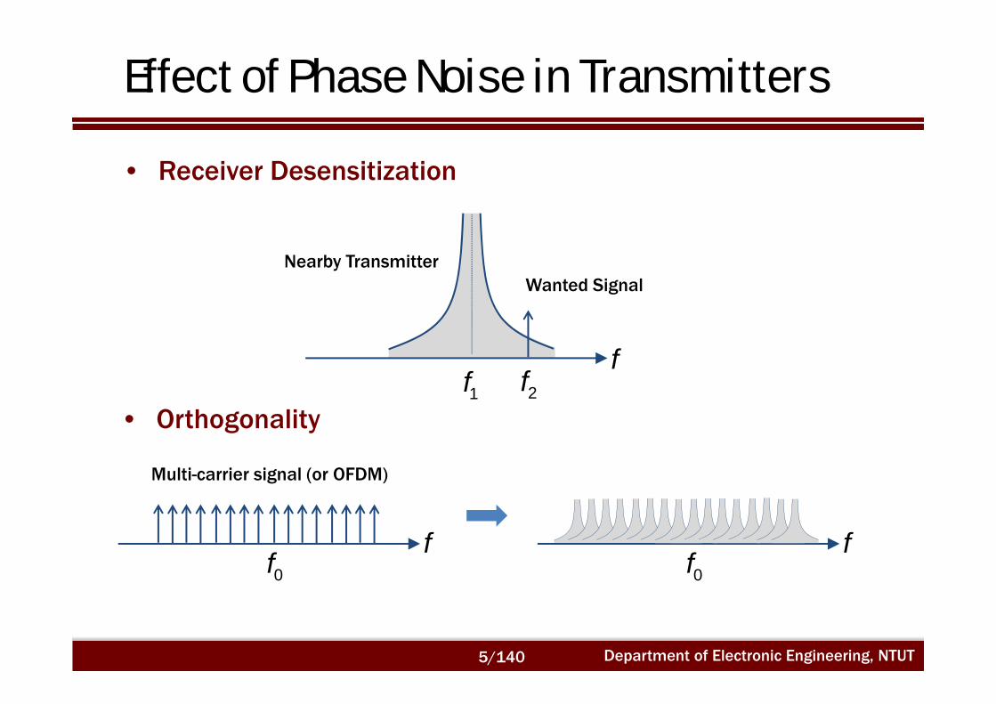
Effect of Phase Noise in Transmitters
f1f
Wanted SignalNearby Transmitter
2f
f0f
Multi-carrier signal (or OFDM)
f0f
• Receiver Desensitization
• Orthogonality
Department of Electronic Engineering, NTUT5/140

Frequency Synthesis
v t
t
• Meaning of frequency synthesisGeneration of a frequency or frequencies that are exact multiples of areference frequency. Usually the reference is very precise and the synthesizedfrequencies are selectable over some range of whole-number multiples of asubmultiple of the frequency at
out refnf fM
where n and M are integers, n varies from Nmin to Nmax, and M is constant.
1T
1
1f
V f
f1f
• Meaning of frequency
reff
Department of Electronic Engineering, NTUT6/140

Transformation to and from Voltage or Current
A B1f
Frequency Discriminator
C D
ddt
Voltage Controlled Oscillator (VCO)
Phase Detector Phase Modulator
1 1v Af2 1f Bv
1 1f dt 2 1v C 2 2Dv
3 2dfdt
V/Hz Hz/V
V/rad or V/cycle rad/V or cycle/V
Department of Electronic Engineering, NTUT7/140

Demonstration of the Transfer Functions
rms rms rms rms rms1 rad 2 V rad rad 11 V 2 V 2 V V 0.32 V
V cycle cycle 2 radAV
Phase Modulator1 rad/V
Phase Detector2 V/Cycle
220 MHz VCO1.5 MHz/V
1 k200 MHz ICO1 MHz/mA
100 MHz signal
Low-pass Filter
50 MHz Cut-off
Frequency Discriminator
5 V/MHz
AB
D
• RMS voltage at point A:
Modulation voltage(1 Vrms at 10 kHz)
1 rmsMHz0.32 V 1.5 0.48 MHz
Vf
rms
20.32 V MHz1 0.32 MHz
1 k mAf
rms5 V0.48 MHz-0.32 MHz 0.8 VMHzDV
C
Department of Electronic Engineering, NTUT8/140

Mathematical Operations on Frequency (I)
• Addition and Subtraction: The Mixer RF
LO
IF
cos 2RF RF RFv t A f t
cos 2 cos 2IF RF LO RF RF LO LOv t v t v t A f t B f t
For the practical mixer with nonlinear operation:
IF RF LOf mf nf
Department of Electronic Engineering, NTUT9/140
cos 2LO LO LOv t B f t
cos 2 cos 22 RF LO RF LO RF LO RF LO
AB f f t f f t
cos2 cos2 for 02 RF LO RF LO RF LO
AB f f t f f t
, cosIF m nv t K m n 2 RF RFf t 2 LO LOf t where and
or we can say the intermediate frequency is:

Mathematical Operations on Frequency (II)
• Frequency Dividers
Subharmonically synchronized oscillators Digital dividers
• Frequency Multiplier Full-wave rectifier (frequency doubler) Harmonically tuned class-C amplifier Step-recovery diode (SRD)
1powerG
N
10/140 Department of Electronic Engineering, NTUT

Frequency Synthesis Techniques
• Direct Analog Synthesis (DAS)
• Direct Digital Synthesis (DDS)
• Indirect Synthesis- Phase-Locked Loops (PLLs)
• Hybrid DDS/PLL
Department of Electronic Engineering, NTUT11/140

Direct Analog Synthesis (DAS) I
• Frequency generated by mixed frequencies
1f2f3f
2Nf1Nf
Nf
outf
filter1
filter2
filter3
filterN-2
filterN-1
filterN
out a bf mf nf
Department of Electronic Engineering, NTUT12/140
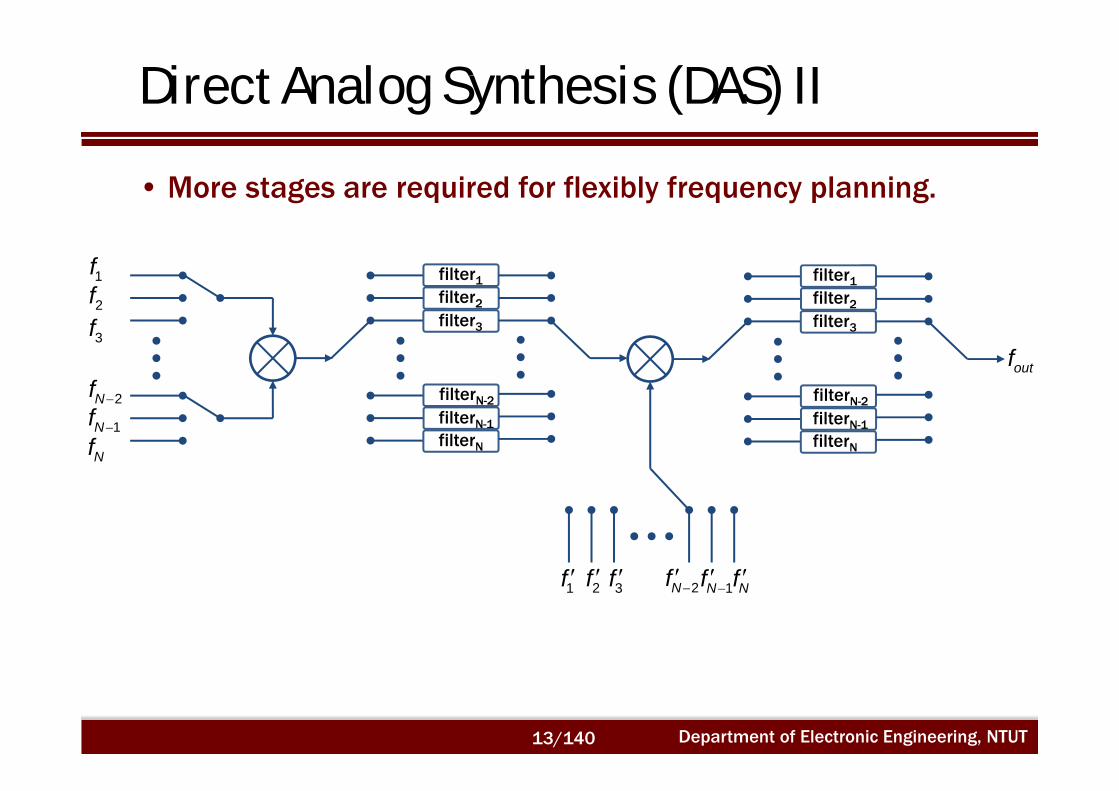
Direct Analog Synthesis (DAS) II
• More stages are required for flexibly frequency planning.
1f2f3f
2Nf1Nf
Nf
filter1
filter2
filter3
filterN-2
filterN-1
filterN
filter1
filter2
filter3
filterN-2
filterN-1
filterN
outf
1f 2f 3f 2Nf 1Nf Nf
Department of Electronic Engineering, NTUT13/140

Direct Digital Synthesis (DDS) I
• Waveform construction is based on the lookup table (LUT)and a digital to analog converter (DAC)
• Direct synthesis• Generated frequency is lower than input frequency
ref cf f
Department of Electronic Engineering, NTUT14/140

Direct Digital Synthesis (DDS) II
• Hardware technique to reduce the spur level of a DDS• Reduce bandwidth
1000MHz
100-150MHz 1100-1150MHz 110-115MHz
div-by-10
DDS FilterFrequency
Divider
0f
outf
BW=50MHz BW=15MHz
reff
Department of Electronic Engineering, NTUT15/140

Hybrid DDS/DAS
• Scheme to increase a DDS output bandwidth
1f 2f 3f 2Nf 1Nf Nf
outf
filter1
filter2
filter3
filterN-2
filterN-1
filterN
DDS FrequencyDivider
reff
Department of Electronic Engineering, NTUT16/140

Indirect Frequency Synthesis (PLL) II
PFD LPF
Frequency Divider
reff outf
/N
• The main goal of the PLL is to sync the divided oscillatorfrequency with the reference frequency outf N reff
out reff N f out reff N f
VCO
Department of Electronic Engineering, NTUT17/140

Fractional-N Frequency Synthesis
• Lower division ratio N to reduce inband phase-noise gain• Effectively produce a fractional division value• Generally employee a delta-sigma modulator for division ratio
dithering
PFD LPF
Dual-modulusFrequency Divider
reff outf
/N, (N+1)
FCW
Department of Electronic Engineering, NTUT18/140

Principle of PLL Operation
vco
con
out reff f
Department of Electronic Engineering, NTUT19/140
• The main goal of the PLL is to sync the divided oscillatorsignal with the reference signal (usually a pure sinusoid).
Phase-Locked Loop Analysis

The Phase-Locked Loop
• PFD: Phase Frequency Detector
• LPF: Loop Filter
• VCO: Voltage Controlled Oscillator
PFD LPF
Frequency Divider
reff outf
/N
VCO
• /N: Divied-by-N Frequency Divider
Department of Electronic Engineering, NTUT21/140

Feedback System
iV s oV s G s
H s
error
o i oV s V s V s H s G s
i oG s V s V s G s H s
1
o
i
V s G sV s G s H s
Department of Electronic Engineering, NTUT22/140
Closed-loop transfer function
G(s)H(s) is the open-loop transfer function
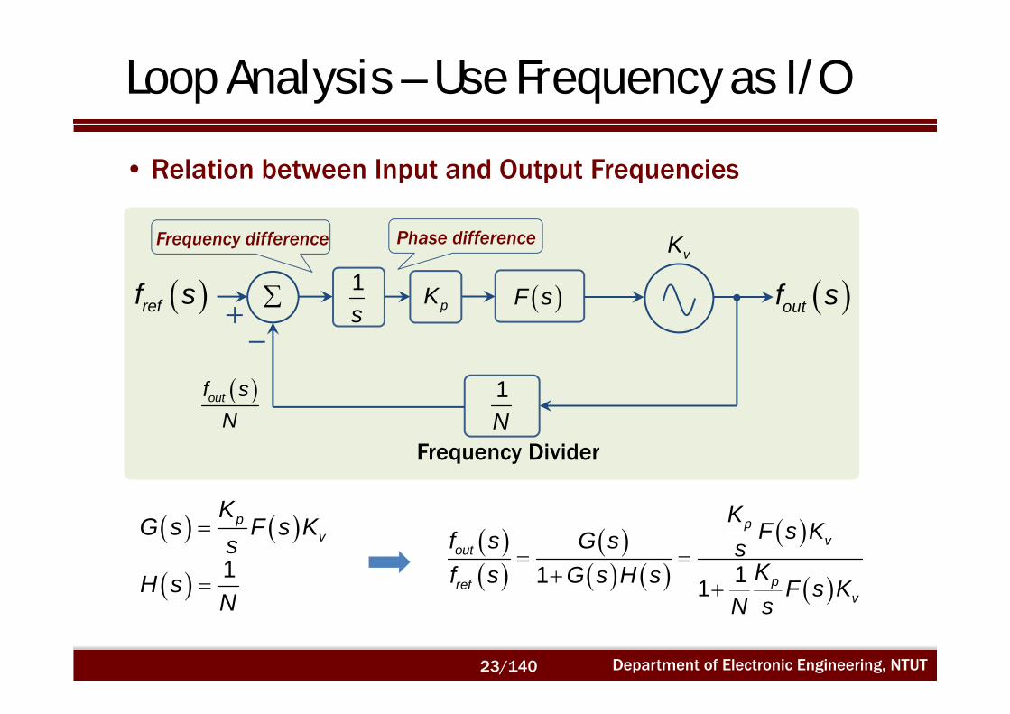
Loop Analysis – Use Frequency as I/O
Frequency Divider
reff s outf s 1s pK F s
vK
1N
Phase differenceFrequency difference
outf sN
• Relation between Input and Output Frequencies
pv
KG s F s K
s
1H sN
11 1
pv
out
prefv
KF s Kf s G s sKf s G s H s F s K
N s
Department of Electronic Engineering, NTUT23/140

Loop Analysis – Use Phase as I/O
Frequency Divider
ref s out s pK F s
vKs
1N
• Relation between Input and Output Phases
Phase difference Frequency to Phase
vp
KG s K F ss
1H sN
11 1
vp
out
vrefp
KK F ss G s sKs G s H s K F s
N s
Department of Electronic Engineering, NTUT24/140

Loop Transfer Functions
0 0
0 01 1p po
i p p
K F s K s K F s K G sT s
K F s K Ns Ns K F s K G s H s
T(s) : closed-loop PLL transfer function
G(s) : forward-path transfer function
F(s) : loop filter transfer function
Kp: phase detector gain
K0/s: VCO transfer function
1 0G s H s
• A PLL is unstable when
1 0 dB@ 180G s H s
The condition of unity open loop gain and a phase angle of 180 degrees mustbe avoided.
H(s) : feedback-path transfer function
G(s)H(s) : open-loop transfer function
or
Department of Electronic Engineering, NTUT25/140

PLL Response without a Loop Filter (I)
0 0
0 01
Fp LPFo
Fi p LPF
KK K K s NT s N NKK K K Ns ss N
• 3 dB cutoff frequency is KF/N = KpKLPFKo/N
LPFF s K
• Without the loop filter, the feedback loop is equivalent to a DC gain ofN plus a low-pass filter with cutoff at .0
log
dB
0FK
N
20logN
3 dB
0
Department of Electronic Engineering, NTUT26/140

PLL Response without a Loop Filter (II)
• The open loop gain has a slope of -6dB/octave or -20dB/decade forall frequencies.
• The phase angle is always -90 degrees at all frequencies. Hencewith no low-pass filter, the PLL is always stable. But the maindrawback is that designers loose control over the loop.
• The simplest PLL is called a type-I loop because the open-loop gainhas one pole at DC (pure integration). It is also a first-order loopbecause the open-loop gain has one significant pole.
p vK F s KG s H s
Ns
Department of Electronic Engineering, NTUT27/140

Single Pole Loop Filter
• The function of the LPF is to filter out any high frequency harmonics inthe loop that might cause the loop to go out of lock, and also tostabilize the loop.
• Adding a LPF also affects the loop response including parameters suchas the loop time response, bandwidth, and the damping factor.
1LPF
p
KF ss
• If we add a low-pass filter with a pole located at , the loop will bestill type-I, but it will become a second-order loop.
1 1
p LPF v F
p p
K K K KN NG s H s
s ss s
p
Department of Electronic Engineering, NTUT28/140

Bode Plot of Forward-path Transfer Function
minLlog m
mG
6 dB/oct1020log FK
10 max20log N
10 min20log N
maxLp1m
90
135
180
mG
12 dB/oct
• Where the curves cross, the open-loop gain equals unity.
1
G sG s H s
N G s N (forward-loop gain )
Department of Electronic Engineering, NTUT29/140

Bode Plot of Open-loop Transfer Function
log m
m mG H
6 dB/oct1020log FK
N
0 dB
Lp1m
90
135
180
mG
12 dB/oct
• Where the curves cross, the open-loop gain equals unity.
1
G sG s H s
N G s N (forward-loop gain )
Phase margin
Department of Electronic Engineering, NTUT30/140

Natural Frequency and Damping ratio
0
0
1
1 1 1 11
F
ppo F
Fi pF
p
p
K
ssK F s K sG s NKT s KG s H s K F s K Ns sNs KsNs
0F p
n p
KN
0
1 1 12 2 2
p pp
n F
NK
is geometric mean of the loop bandwidth in the absenceof a filter and the filter corner frequency.
2
2 2 2 22 2 2
p F p F n
p F n n n np
K KNK s s s ss s
N
Characteristics equation
• Prototype second-order equation
•Natural frequency
•Damping ratio
Department of Electronic Engineering, NTUT31/140

Closed-Loop Gain for Large Damping Ratio
As long as damping ratio is greater than one, the poles are real and atangential plot of closed loop gain looks
20logN
6 dB/oct
12 dB/oct
log m
out
ref
f sf
2 202 1 1 1
21 1 1
2p
The characteristics are similar to the case with no loop filter, except for theincreasing rate of attenuation in fout/fref beyond approximately the filtercorner frequency .
2 1p n ns • The poles of the closed-loop function are located at
0
p
Department of Electronic Engineering, NTUT32/140
p

Close-loop Responses
0F p
n p
KN
0
1 1 12 2 2
p pp
n F
NK
• As decreases toward , the damping ratio decreases and the phase shiftat increases. Correspondingly, the transient response of the loop becomesless damped (more ringing) and the response peaks near .
p 00
n
m n 0m
• For large damping, the response is similar to that for no filter but, as thedamping ratio decreases, the response peaks and the peak moves to a lowerfrequency relative to .0
Department of Electronic Engineering, NTUT33/140

Relative Stability – Phase Margin
• Left figure shows the phase margin(relative stability) as a function of thedamping factor. More highly dampedloops are safer, in that moreparameter variation is allowablebefore instability occurs.
log m
m mG H
6 dB/oct1020log FK
N
0 dB
Lp1m
90
135
180
mG
12 dB/oct
Phase margin
• With a single-pole low-pass filter, theloop is inherently stable, sine -180o
phase shift cannot be attained for anyfinite frequency. (not always true practically)
Department of Electronic Engineering, NTUT34/140

Transient Response
reff outf G s
1 N
e
1N2N
1 refN f2 refN f
2 1N N
e
1
2
1 refN fN
t
0t toldf
newf
Synthesizer output frequency
A
B
CD
Overshot
Ringing • Lower damping ratio bringsa higher percent overshootcan cause the loop to goout of lock. (more unstable)
• Narrower bandwidth withsmaller damping ratio andlonger settling time.
Department of Electronic Engineering, NTUT35/140
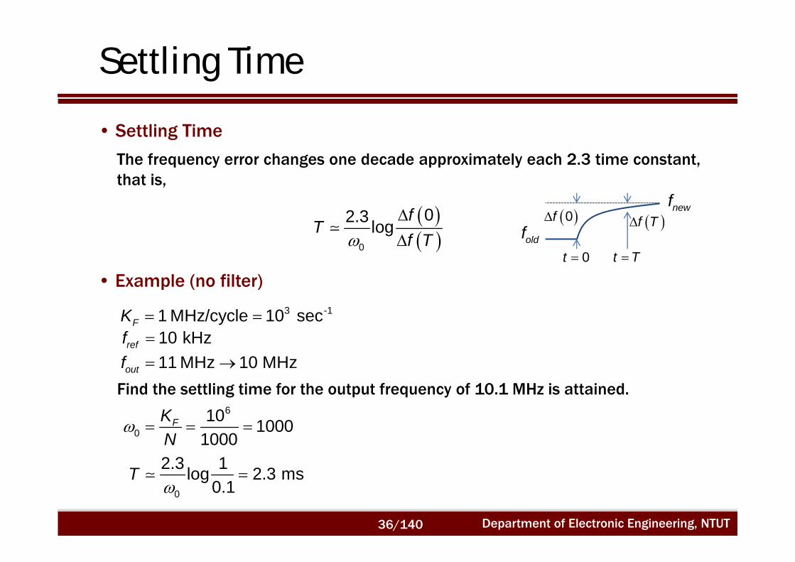
Settling Time
• Settling Time
The frequency error changes one decade approximately each 2.3 time constant,that is,
0
02.3 logf
Tf T
oldf
newf 0f
0t t T
f T
• Example (no filter)
3 -11 MHz/cycle 10 secFK 10 kHzreff 11 MHz 10 MHzoutf
Find the settling time for the output frequency of 10.1 MHz is attained.6
010 1000
1000FK
N
0
2.3 1log 2.3 ms0.1
T
Department of Electronic Engineering, NTUT36/140

A Pole-Zero Filter
• A pole-zero filter is a low pass filter with a pole frequency and azero frequency . The addition of a pole in the transfer functioncauses the transfer function slope to drop at a rate of 6 dB per octavewhereas the addition of a zero in the PLL transfer function has theopposite effect. The pole-zero filter transfer response is given by
11
z
p
sF s
s• The open loop transfer function is:
1
1p v zp v
p
K K sK F s KG s H s
Ns Ns s
pz
6 dB/oct
12 dB/oct
log mzp
6 dB/oct
• The closed-loop transfer function is:
0
01po
i p
K F s K sT s
K F s K Ns
Department of Electronic Engineering, NTUT37/140
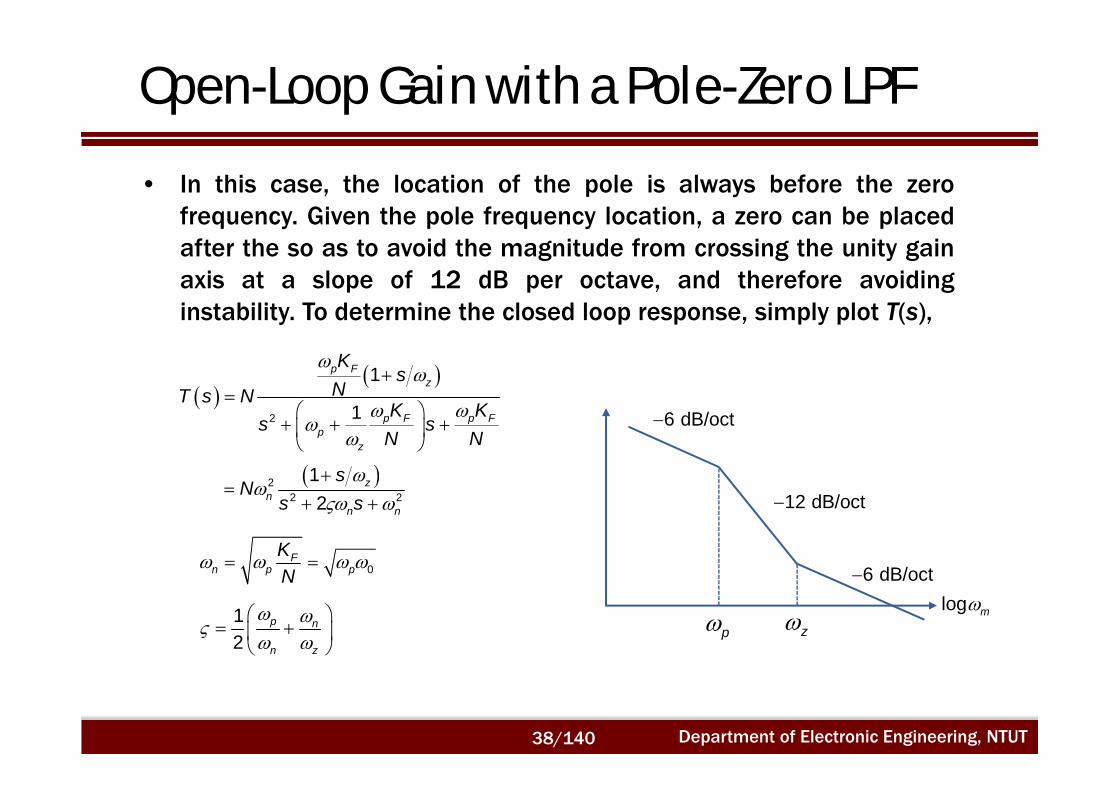
Open-Loop Gain with a Pole-Zero LPF
• In this case, the location of the pole is always before the zerofrequency. Given the pole frequency location, a zero can be placedafter the so as to avoid the magnitude from crossing the unity gainaxis at a slope of 12 dB per octave, and therefore avoidinginstability. To determine the closed loop response, simply plot T(s),
2
1
1
p Fz
p F p Fp
z
Ks
NT s NK K
s sN N
0F
n p pKN
12
p n
n z
6 dB/oct
12 dB/oct
log mzp
6 dB/oct
22 2
12
zn
n n
sN
s s
Department of Electronic Engineering, NTUT38/140

Open-Loop Gain with a Pole-Zero LPF
• From the results, selecting the pole frequency sets the naturalfrequency (and subsequently the loop bandwidth) and selecting thezero (based on the pole location in the open loop gain response)determines the desired percentage overshoot. Therefore, a pole-zerofilter allows the designer to select the loop bandwidth and thedamping factor independently and still achieve stability.
0F
n p pKN
12
p n
n z
Department of Electronic Engineering, NTUT39/140

Components in PLLs

Phase Detector (PD) – Mixer
1 2cosd dv A
2i i if
1 2coss sv A
• The balanced mixer
IF d sv v v
1 2 1 1 2cos cos 4IF d sv A A f t
1 2f fFor filtered-out by the LPF
1 2
2
1 2 2
IF dv A
and is very small
1 1 12 f
2 2 22 f
IFvPhase of signal 1
Phase of signal 2
Department of Electronic Engineering, NTUT41/140
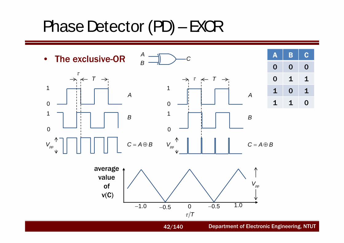
A B C
0 0 0
0 1 1
1 0 1
1 1 0
Phase Detector (PD) – EXOR
AB
C
1
01
0
T
A
B
ppV C A B
average value
of v(C)
ppV
1.0 0.5 0 0.5 1.0T
• The exclusive-OR
1
01
0
T
A
B
ppV C A B
Department of Electronic Engineering, NTUT42/140

Phase Detector (PD) – SR-FF
S
R
QA
B
C
T
Av
Bv
ppV
Cv
0 1 2
average value
of v(C)
T
ppV
A B C
0 0 N
0 1 0
1 0 1
1 1 X
• S-R Flip-Flops
Department of Electronic Engineering, NTUT43/140

Phase/Frequency Detector (PFD)
A lagging B ( same )
• Detectable range : -2π~ 2π
CLK
DQ
CLR
Q
DCLR
CLK
A
B
1
QA
QB
A
B
QA
QB
A BQ Q
2 4
24
A leading B ( same )
A
B
QA
QB
Department of Electronic Engineering, NTUT44/140

Two General Types of PFD
Tt
ref(t)
div(t)
ref/2(t)
div/2(t)
e(t)1
-1
• XOR-Based PFD
ref(t)
div(t)
up(t)
dn(t)
e(t)
1
0
-1 Tt
• Tri-state PFD
Department of Electronic Engineering, NTUT45/140

Typical Dead-Zone for Various PFDs
Type Dead Zone
Conventional ~800ps
NC-PFD ~160ps
TSPC-PFD ~210ps
MPTPFD ~10ps
• Commercial product Motorola MC4044 using conventional PFDintroduce 30 degree dead-zone@20MHz (~400ps).
• The first XOR-based dead-zone free design was proposed by AnalogDevice (AD9901).
1f
2f
UP
UP
DN
DN
Department of Electronic Engineering, NTUT46/140

Dead-zone Problem of PFDs
• In a PLL, the contribution of every block is essential to thetotal phase noise if a high-quality frequency synthesizer isthe goal.
• If the input frequency reference to be compared is as high asseveral MHz, the linearity of the phase detector becomesessential.
• In the passband of the PLL, the output phase noise dependson noise contribution from the phase detector, loop filter andfrequency divider.
• In charge pump based PLL, there are more problems.
Department of Electronic Engineering, NTUT47/140

The Principle of PFD and Dead-Zone Problem
• The PFD operates as a frequency detector initially and asphase detector finally to achieve loop lock.
• The dead-zone problem:- When two signals have the same frequency and almost identical
phase, the PFD block is not able to generate a proper output signalso that an identical phase may be obtain.
- This uncertainty leads to phase noise (jitter in time domain) andgeneration of spurious at the output of VCO.
AND gate switch threshold
ref(t)
div(t)
up(t) dn(t)
1
0
1
0
ref(t)
div(t)
up(t)
1
0
1
0
dn(t)
ref(t)
div(t)
1
0
1
0
up(t)dn(t)
Department of Electronic Engineering, NTUT48/140

Solve the Dead-Zone Problem
• Delayed reset path• Inphase operation• Need accurate timing analysis• Low spurious tones• Bad linearity
• Alternatively current output• Non-inphase operation• More power consumption at lock state• Current mismatch with CP is the issue• High spurious tones• Good linearity
• XOR-Based PFD
• Tri-state PFD
Department of Electronic Engineering, NTUT49/140
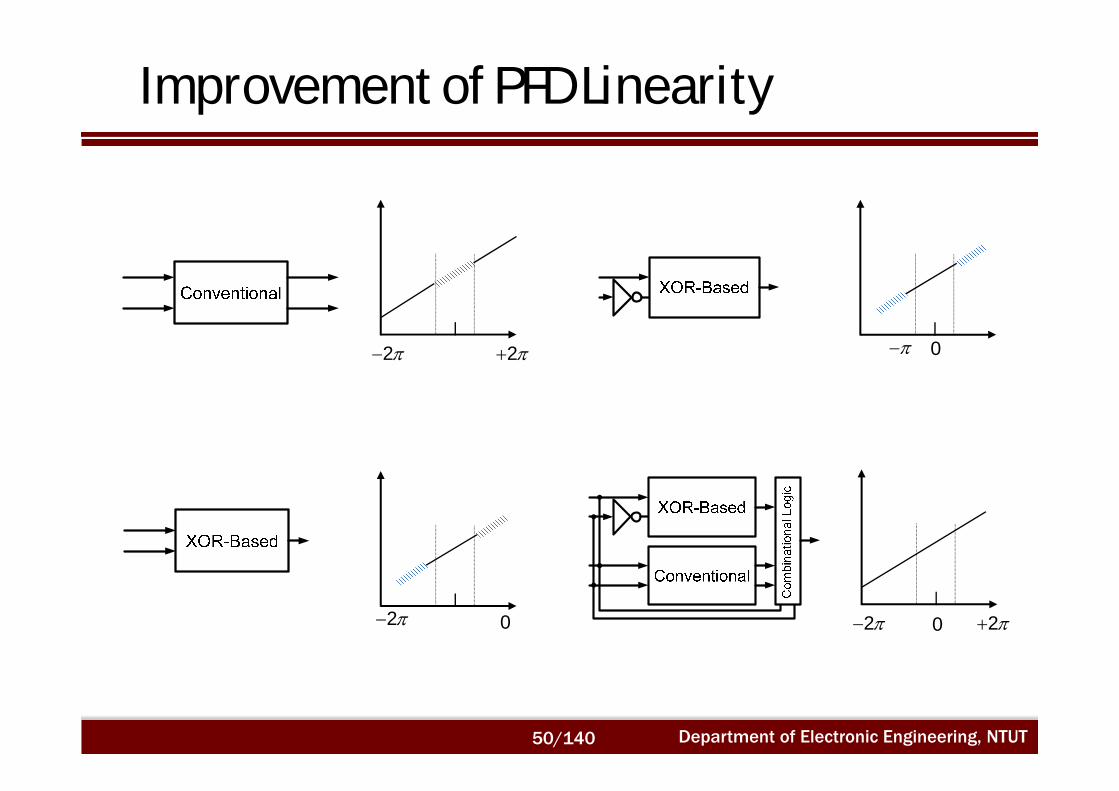
Improvement of PFD Linearity
22
2 0
0
22 0
Department of Electronic Engineering, NTUT50/140

Charge-Pump Phase Detector
• The most popular phase-detector type is both a charge-pump (CP)detector and a phase-frequency detector (PFD), the terms, thecharge-pump PD and PFD, are sometimes interchangeably.
• The PFD acts as a phase detector during lock and provides afrequency-sensitive signal to aid acquisition when the loop is out oflock.
• The charge pump is so named because it is supposed to deliver acharge proportional to phase error to the loop filter.
PFD ChargePump
Switched Output(analog)
Charge Up
Charge Down
CU (digital)
CD (digital)
RD
VD
Department of Electronic Engineering, NTUT51/140
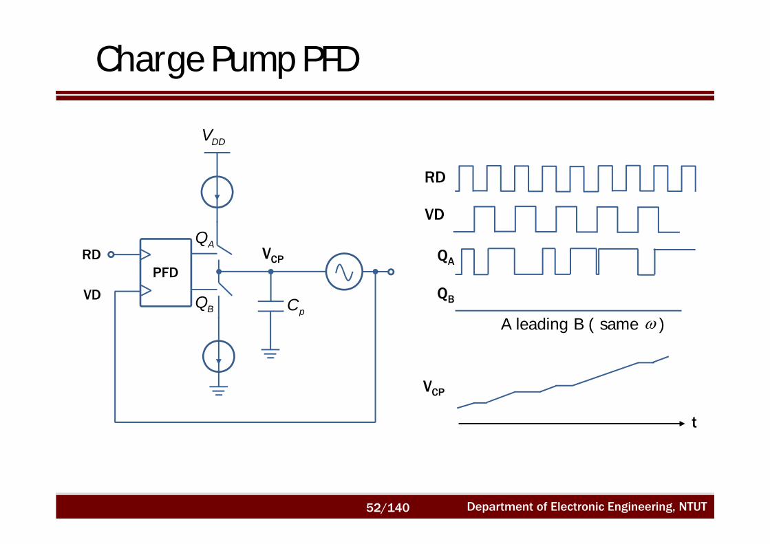
Charge Pump PFD
PFD
AQ
BQpC
DDV
A leading B ( same )
RD
VD
QA
QB
VCP
VCP
t
Department of Electronic Engineering, NTUT52/140
RD
VD

Charging Current
RD
VD
CU
CD
Current Out
Department of Electronic Engineering, NTUT53/140

Charge Pump (Current Source and Sink)
PFD
AQ
BQ
DDV
RD
VD
LZ
oV
DDV
R
1M 2M
1
1
WL
2
2
WL
2D oI I1DI
GSVoV
sink current
211 2
DD GSD GS thn
V VI V VR
222 2D GS thnI V V
2 2 2 2 2
1 1 1 1 1
D
D
I W L WI W L W
DDV
R
1M 2M1
1
WL
2
2
WL
2D oI I
1DI
SGV
oV
source current
211 2
DD SGD SG thp
V VI V VR
222 2D SG thpI V V
2 2 2 2 2
1 1 1 1 1
D
D
I W L WI W L W
• Saturation region:
DS GS thnV V V
GS thnV V
• Saturation region:SD SG thpV V V
SG thpV V
Department of Electronic Engineering, NTUT54/140

Early Effect
DDV
R
1M 2M
1
1
WL
2
2
WL
2D oI I1DI
GSVoV
sink current
222 ,1
2D GS thn DS DS satI V V V V
1L
• Channel length modulation and Early effect
DI
DS oV V
(prefer a long channel length)
2
1 1Ao
D o D
VrI I I
(prefer a high output resistance)
Department of Electronic Engineering, NTUT55/140

Cascode Connection and Switch
3 3 2 21o o m o oR r g r r
DI
DS oV V
• Cascode connection increasesoutput resistance
PFD
AQ
BQ
DDV
RD
VD
LZ
oV
DDV
R
1M 2M
1
1
WL
2
2
WL
2D oI I1DI
GSV
oV
sink current
BQ
switch
3M
2 thnV V
• Need excess gate-sourcevoltage V
BQ is a digital signal (0~VDD)
thnV
Cascoded (with switch)
Department of Electronic Engineering, NTUT56/140

Current Mismatch
DI
DS oV V
Department of Electronic Engineering, NTUT57/140

Spurs and CP Non-ideal Effect
tsource
toff
tsink
Isink
Isource
tcomp
• Reference Spurs- current leakage- current source mismatch(a) current mismatch with different
output node voltage(b) unequal switching time
• Non-reference Spurs- crosstalk(a) dual loop(b) interferences
- non-crosstalk(a) fractional spurs(b) interferences(c) dual loop references mixing(d) prescaler miss counting
Department of Electronic Engineering, NTUT58/140

Charge-Pump Switching Time
• When the charge-pump(CP) based PLL is used, the CP isalso the bottle neck since the PFD can’t distinguish inputedges separated by less than the CP switching time.
CPI
CPI
PFDPFD
CP
CP
Department of Electronic Engineering, NTUT59/140
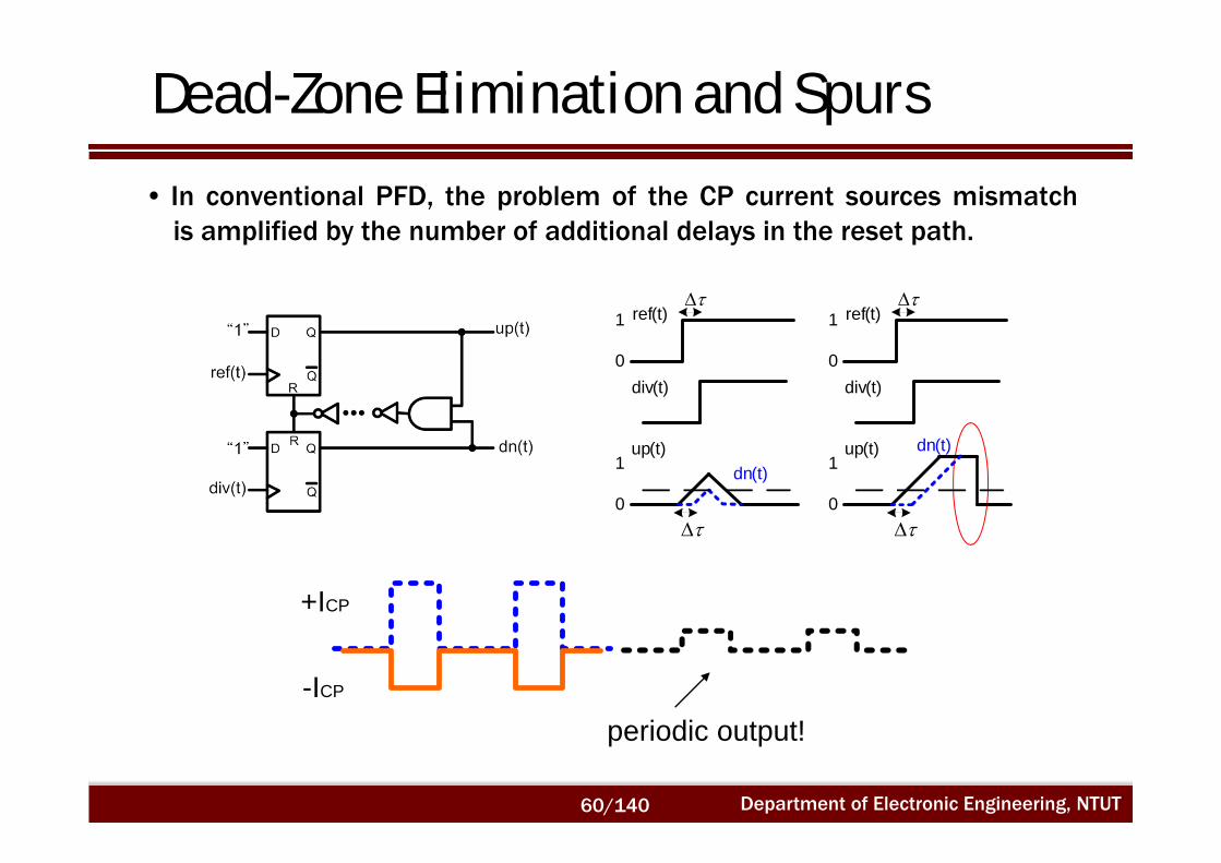
Dead-Zone Elimination and Spurs
• In conventional PFD, the problem of the CP current sources mismatchis amplified by the number of additional delays in the reset path.
ref(t)
div(t)
1
0
1
0
up(t)dn(t)
ref(t)
div(t)
1
0
1
0
up(t) dn(t)
periodic output!
+ICP
-ICP
Department of Electronic Engineering, NTUT60/140

Dead-Zone Issues
• In charge pump based PLL, the dead-zone problem is notonly considered in PFD design but charge pump.
• As reference frequency goes higher, the dead-zone issue ismore serious, because the linearity highly depends on thedead-zone.
• In charge pump design, it’s hard to achieve low powerconsumption, fast current switching and perfect currentmismatch.
Department of Electronic Engineering, NTUT61/140
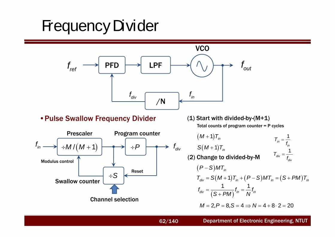
Frequency Divider
PFD LPFreff outf
/N
VCO
divf inf
/ 1M M
Prescaler
P
S
infdivf
Program counter
Swallow counter
Reset
Modulus control
Channel selection
•Pulse Swallow Frequency Divider
1in
in
Tf
1 inM T
1 inS M T
inP S MT
1div in in inT S M T P S MT S PM T
(1) Start with divided-by-(M+1)Total counts of program counter = P cycles
(2) Change to divided-by-M1
divdiv
Tf
1 1
div in inf f fS PM N
2, 8, 4 4 8 2 20M P S N
Department of Electronic Engineering, NTUT62/140

Asynchronous Divider
J Q
KC
J Q
KC
J Q
KC
1
1
1
1
1
1inf
2inf
4inf
8inf
inf2inf4inf8inf
outf
inf
2inf
4inf
8inf
outf
Department of Electronic Engineering, NTUT63/140

Synchronous Divider (2 versions)
J Q
KC
J Q
KC
J Q
KC
J Q
KC
J Q
KC
1
1
2inf 4inf8inf
16inf
16inf
Department of Electronic Engineering, NTUT64/140

Spikes in Synchronous Divider
2inf4inf8inf
outf
2inf
4inf
8inf
outf
2inf late
8inf early
• Racing in synchronous divider producing output spikes
Department of Electronic Engineering, NTUT65/140

Synchronous Divider w/ Enable
J Q
KC
J Q
KC
J Q
KC
J Q
KC
J Q
KC
J Q
KC
1
1
J Q
KC
J Q
KC
J Q
KC
J Q
KC
J Q
KC
J Q
KC
1
1
•Parallel Enable
•Serial Enable
Department of Electronic Engineering, NTUT66/140

Direct Variable Frequency Divider
Department of Electronic Engineering, NTUT67/140

Type and Order of the Loop
Frequency Divider
ref s out s pK F s
vKs
1N
1
G s N sT s
G s H s D s
• The simplest PLL is the type-I loop because the open-loop gain hasone pole at DC (pure integration). It is also a first-order loop becausethe open-loop gain has one significant pole.
11 0
n nn nN s a s a s a
1
1 0m m
m mD s b s b s b
Order = m (m roots)Type = n (n roots at DC)
Department of Electronic Engineering, NTUT68/140

Filter First-order Type 1
• First order, type I (no filter)
1Riv
ov
2R
Llog m0 dB
G
6 / .dB oct
2
1 2
oLPF
i
v RGv R R
A3R
iv
4R
ov A
4
3
oLPF
i
v RGv R
Department of Electronic Engineering, NTUT69/140

Filter Second-order Type I
• Second order, type I (Lag-and-lead filter)
1Riv
ov
2R
1C
A3R
iv
5R
ov
2C
4R
Llog m0 dB
G
12 / .dB oct
6 / .dB octzp
1
1z
LPF
p
s
G s
2 1
1z R C 1 2 1
1p R R C
1
1z
LPF
p
s
G s
4 52
4 5
1z R R C
R R
5 2
1p R C
Department of Electronic Engineering, NTUT70/140

Filter Second-order Type 1
• Second order, type I (Lag filter)
1Riv
ov
2R1C
Llog m0 dB
G
6 / .dB oct
p
12 / .dB oct
A3R
iv
4R
ov
2C
A
2
1 2
1
1LPF
p
RG sR R
4
3
1
1LPF
p
RG sR
1 1 2
1 1 1p C R R
4 2
1p R C
Department of Electronic Engineering, NTUT71/140

Filter Second-order Type II
• Second order, type II (Integrator and lead filter)
Llog m0 dB
G12 / .dB oct
6 / .dB octz
A1R
iv
2R
ov
C
A
1 1
11 z
LPF
s
GR C s
2
1z R C
Department of Electronic Engineering, NTUT72/140

Filter Third-order Type II
• Third order, type II (Integrator plus lead-lag filter)
Llog m0 dB
G12 / .dB oct
p
12 / .dB oct6 / .dB octz
A1R
iv
2R
ov
2C
1C
A
A3R
iV
4R
oV
3C
5R
4CA
1 1
11
1
zLPF
p
s
GR C ss
3 3
11
1
zLPF
p
s
GR C ss
2 1 2
1z R C C
2 2
1p R C
4 3
1z R C
5 4
1p R C
Department of Electronic Engineering, NTUT73/140

Filter Third-order Type II
• Third order, type I (imperfect integrator plus lead-lag filter)
Llog m0 dB
G6 / .dB oct
2p
12 / .dB oct6 / .dB octz 1p
12 / .dB oct
A
1oA R
A
A
Department of Electronic Engineering, NTUT74/140

Oscillator
• Oscillator provides a sinusoidal signal
v t
t
1
1f
V f
f1f
v t
t
1
1f
V f
f1f
Department of Electronic Engineering, NTUT75/140

Voltage Controlled Oscillator (VCO)
• VCO is an oscillator of which frequency is controlled by atuning voltage
• VCO is a simple FM modulator
vcof
tuneV
tuneV
Department of Electronic Engineering, NTUT76/140
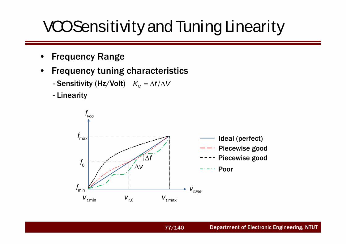
VCO Sensitivity and Tuning Linearity
• Frequency Range
• Frequency tuning characteristics- Sensitivity (Hz/Volt)
- LinearityVK f V
vcof
tunev,0tv
0f
maxf
minf,mintv ,maxtv
vf
Ideal (perfect)Piecewise goodPiecewise good
Poor
Department of Electronic Engineering, NTUT77/140
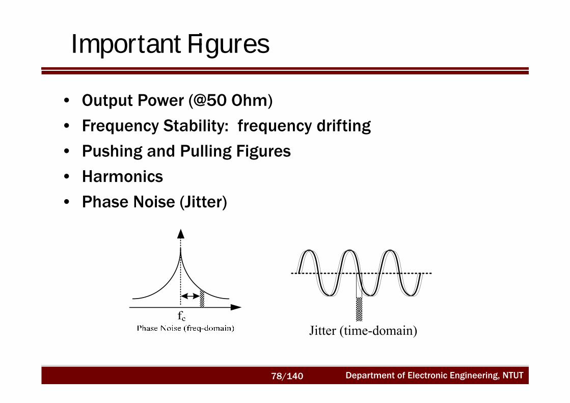
Important Figures
• Output Power (@50 Ohm)
• Frequency Stability: frequency drifting
• Pushing and Pulling Figures
• Harmonics
• Phase Noise (Jitter)
Department of Electronic Engineering, NTUT78/140

Phase Noise and Jitter
1 Hz10log 10log dBc Hz
2noise
carrier
S fPL f
P
• Phase Noise
• Jitter
Cycle jitter
cn nT T T 2
1
1limN
c cnn nT
N
Cycle-to-cycle jitter
1ccn n nT T T 2
1
1limN
c ccnn nT
N
Absolute jitter (long-term jitter, accumulated jitter) of N cycles
1 1
N N
abs n cnn n
T N T T T
2
1
1limN
c ccnn nT
N
for white noise sources 0
2abs ccfT t t and 2cc c
Department of Electronic Engineering, NTUT79/140

Relation of Phase Noise and Jitter
• Relationship between the SSB phase noise and the rms cycle jitter: (Weigandt et al.)
3 20
2cfL f
f
• Relationship between the SSB phase noise and the rms cycle jitter: (Herzel and Razavi)
3 20
22 3 40
4
8cc
cc
L
• Self-referred jitter and phase noise with white noise: (Demir et al.)
20
2 2 4 20
f cL ff f c
2 t t c 20
2 ccfc
Department of Electronic Engineering, NTUT80/140

Oscillator Design (I)
• Feedback : Barkhausen’s Criteria
( )( )1 ( ) ( )
of
i
V G sG sV G s H s
( ) ( ) 1G s H s (Phase is 0 deg. or multiple of 360 deg.)
Department of Electronic Engineering, NTUT81/140

Oscillator Design (II)
'11 1G S
'22 1L S
If the two-port network is oscillating at one port, it must be simultaneouslyoscillating at the other port.
• Two Port ReflectionSine the resonator is passive, thus 1G
Department of Electronic Engineering, NTUT82/140

Oscillator Design (III)
0)()( DRR
0)()( DXX
• One-port Negative Resistance
Department of Electronic Engineering, NTUT83/140

Common Oscillator Configurations
bici
C
E
B
1C
2C
3Lbi
ci
C
E
B
1L
2L
3C
bici
C
E
B
1C
2C
3Lbi
ci
C
E
B
1C
2C
3L
Colpitts Hartley
Clapp Siler
Department of Electronic Engineering, NTUT84/140
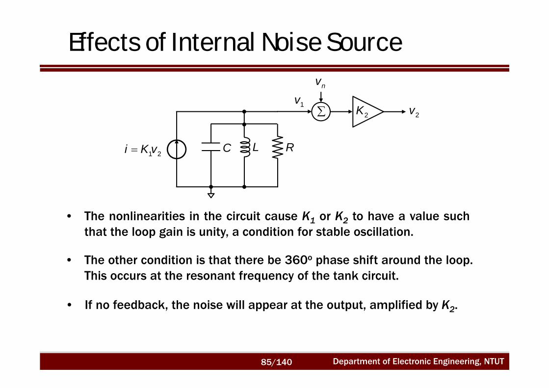
Effects of Internal Noise Source
• The nonlinearities in the circuit cause K1 or K2 to have a value suchthat the loop gain is unity, a condition for stable oscillation.
• The other condition is that there be 360o phase shift around the loop.This occurs at the resonant frequency of the tank circuit.
2K
RC L1 2i K v
1v
nv
2v
• If no feedback, the noise will appear at the output, amplified by K2.
Department of Electronic Engineering, NTUT85/140

Small Noise Introduced
• But what effect does the feedback have?(1) Far from spectral center: the output contains amplified circuit noise
(2) Close to spectral center: the feedback has an important effect
11 1
iT
v Zi j C
R LPhase shift of this factor is
1 1tanT R C
L
2K
RC L1 2i K v
1v
nv
2v
Department of Electronic Engineering, NTUT86/140

Tank Phase Shift
0 0
2Td Qd
Q is the loaded quality factor of the frequency-determining circuit.
• For modulation rates small compared to one-half ofthe resonant bandwidth of ZT, a change infrequency causes a phase change in thetransfer function, where the two changes are
2osc
Q
0
10
0
1tan 0T R CL
0
T
0
TH
1
Department of Electronic Engineering, NTUT87/140
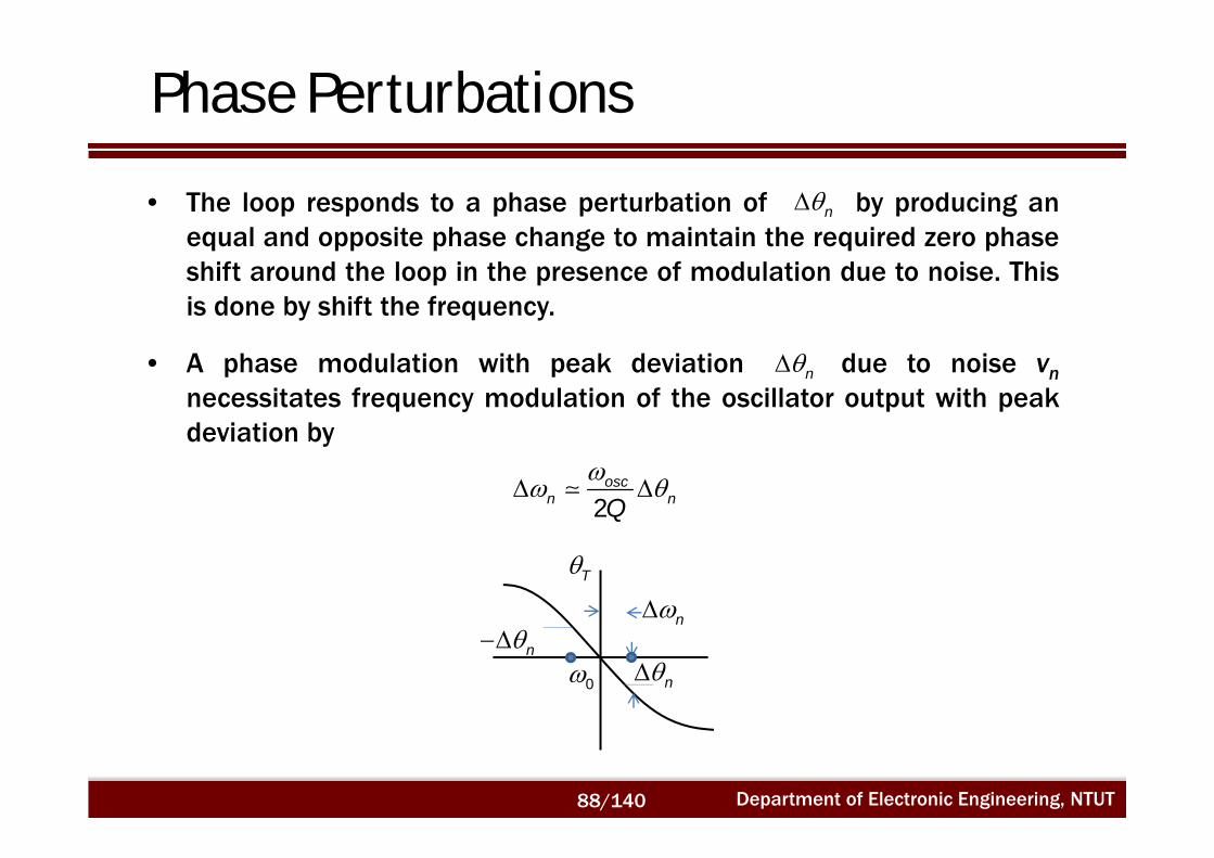
Phase Perturbations
• The loop responds to a phase perturbation of by producing anequal and opposite phase change to maintain the required zero phaseshift around the loop in the presence of modulation due to noise. Thisis done by shift the frequency.
• A phase modulation with peak deviation due to noise vnnecessitates frequency modulation of the oscillator output with peakdeviation by
2osc
n nQ
n
n
0
T
n
nn
Department of Electronic Engineering, NTUT88/140

Closed-Loop Noise
2 2oscn
nm mQ
where is the noise modulation frequency.
2
osc
Q 1
m
n
n 2
• The phase noise would ordinarily appear at the output due to circuitnoise is accentuated by a factor . 2osc mf Qf
m
2osc
mffQ
log mf
Open loop
Closed looplogS
2rad Hz
Department of Electronic Engineering, NTUT89/140

Oscillator Phase Noise
f0f mff 0
1 Hz
RPV avs
avsRMS
RFkTVnRMS 11 HzR
FkTVnRMS 2
• The input phase noise in a 1-Hz bandwidth at any frequency from the carrier produces a phase deviation.
0 mf f
sPnP
Department of Electronic Engineering, NTUT90/140
Noise

Noise Caused Phase Deviation
1nRMSpeak
avsRMS avs
V FkTV P
112RMS
avs
FkTP
RMS totalavs
FkTP
Noise
212RMS
avs
FkTP
(total phase deviation)
12 nRMSV
m
2 avsRMSV
0
peak
Department of Electronic Engineering, NTUT91/140

Lesson’s Model (I)
avsRMSm P
FkTBfS 2)(
1)(B dBm/Hz 174 kTB
S
cfmf
avsPFkTB
1)(B 1)(
m
c
avsm f
fP
FkTBfS
• The spectral density of phase noise :
(theoretical noise floor of the amplifier)
• Flicker Noise
The purity of signal is degraded by the flicker noise at the frequencies close tothe carrier.
noise floor
flicker noise
Department of Electronic Engineering, NTUT92/140

Lesson’s Model (II)
)2(1
1)(
0
loadm
m QjL
in
Equivalent lowpass forresonator
out
+)( min f
)(2
0min
mL
fQj
• The oscillator may be modeled as an amplifier with feedback
0
1( )21
L mL m
HQj
0
2 2L
BQ
0( ) 1 ( )2out m in m
L m
f fj Q
2
0 2
1( ) 1 ( )2out m in m
m L
fS f S ff Q
( ) 1 cin m
avs m
fFkTBS fP f
( )L mH
Department of Electronic Engineering, NTUT93/140

Lesson’s Model (III)
22
3 2 21 1L( ) 1
2 4 2o c o c
mavs m L m L m
f f f fFkTBfP f Q f Q f
Up-convert 1/f noise
Thermal FM noise
Flicker noise
Thermal noise floor
• Lesson’s Oscillator Model:
slope
fcf
f1
Thermal Noise Floor
1/f noise at carrier
0f
C
2
0 2
1 1L( ) 1 ( )2 2m in m
m L
ff S ff Q
( ) 1 c
in mavs m
fFkTBS fP f
Open-loop amp.Closed-loop with resonator
Department of Electronic Engineering, NTUT94/140

Lesson’s Model (IV)
1mf
1mf 0
mf
3mf
1mf
2mf
3mf
0mf
cf
cf
cf
cfQfo
2 Qfo
2
avsPFkTB
avsPFkTB2
avsPFkTB
High Q OscillatorPhase perturbation
Low Q OscillatorPhase perturbation
Resulting phase noise Resulting phase noise
Department of Electronic Engineering, NTUT95/140

Noise Analysis

PLL Phase Noise Model
Frequency Divider
,ref n
out
1N
PFD LPF
,pfd nV ,op nV
,vco n
,div n
VCO
Xtal
Department of Electronic Engineering, NTUT97/140

Noise Transfer Functions (I)
, , , , , ,out n pfd n op n ref n div n e vco nd
T sV V T s H s
K
1
G sT s
G s H s
1
1eH sG s H s
for for1
c
c
NG sT s
G sG s H s
for 1
for11
ce
c
NG sH s
G s H s
Department of Electronic Engineering, NTUT98/140

Noise Transfer Functions (II)
clog m
1
G sG s H s
N
G s
Transfer function multiplying all sources except VCOc
log m
1
1 G s H s1
1
G s H s
Transfer function for VCO
clog m
20logN G s
dB
0
Department of Electronic Engineering, NTUT99/140

Typical VCO and PLL Noise Performance
Department of Electronic Engineering, NTUT100/140

PLL Design with Sheets
http://www.peregrine-semi.com
Department of Electronic Engineering, NTUT101/140

Phase-Locked Loop Architectures
• Integer-N PLL• Fractional-N PLL• Offset PLL• DDS Offset PLL• Dual Loop PLL• Multi-Loop PLL
Department of Electronic Engineering, NTUT102/140

Offset PLL
out ref offsetf N f f
• Lower division ratio N to reduce inband phase-noise gain
?
PFD LPF
Frequency Divider
reff outf
/N
offsetf
• Extend bandwidth with different offsetf• Avoid LO pulling
Department of Electronic Engineering, NTUT103/140

Dual-Loop PLL (I)
PFD LPF
Frequency Divider
reff outf
/N
offsetf
PFD LPF outf
/M2nd loop
Department of Electronic Engineering, NTUT104/140

Dual-loop PLL (II)
PFD LPF
Frequency Divider
1reff
outf/N
1f
PFD LPF
2f
/M2nd loop
2reff
Department of Electronic Engineering, NTUT105/140

Multi-Loop PLL
3rd loop
2nd loop
foffset1
PFD LPF
/N
foutVCOfref
PFD LPF
/M
VCO
foffset2
PFD LPF
/P
VCO
foffset3
Department of Electronic Engineering, NTUT106/140

DDS Offset PLL
PFD LPF
Frequency Divider
reff outf
/N
offsetf
DDS
Department of Electronic Engineering, NTUT107/140

Fractional-N Frequency Synthesis
• Lower division ratio N to reduce inband phase-noise gain• Effectively produce a fractional division value• Generally employee a delta-sigma modulator for division
ratio dithering
PFD LPF
Dual-modulusFrequency Divider
reff outf
/N, (N+1)
FCW
Department of Electronic Engineering, NTUT108/140

DDS-Driven Fractional-N Synthesizer
• DDS acts a reference source or phase/frequency modulator• A variable reference frequency source can drive a fractional
frequency output.
PFD LPF
Frequency Divider
reff outf
/N
DDS
FCW
Hybrid DDS/PLL
Department of Electronic Engineering, NTUT109/140
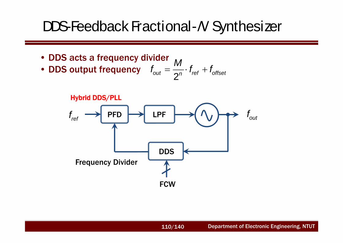
DDS-Feedback Fractional-N Synthesizer
• DDS acts a frequency divider• DDS output frequency
Hybrid DDS/PLL
PFD LPF
Frequency Divider
reff outf
DDS
FCW
2out ref offsetn
Mf f f
Department of Electronic Engineering, NTUT110/140

Comparison of Frequency Synthesizers
DDSSingle-Loop
PLL
Multi-Loop
PLLDDS/DAS
DDS Offset
PLL
DDS Driven
PLL
BW
(output)
Narrow
< 100MHz
Broad
> 1GHz
Broad
> 1GHz
Broad
> DDS
Broad
(carefully design)
Broad
ResolutionExtremely
Fine
< 0.02 Hz
Very Course
> 250kHz
(typical)
Medium
> 1kHz
(typical)
Extremely Fine
< 0.01 Hz
Extremely Fine
< 0.01 Hz
Extremely Fine
< 1Hz
Switching
Time
Very Fast
< 100 ns
Fast
< 100us
(typical)
Very Slow
> 1ms
(typical)
Very Fast
< 1us
(limited by RF switch)
Fast
< 100us
(typical)
Trade-off vsclose-in spurious
tones
Spurious
Noise
< 75dBc
(limited by DAC)
Very GoodGood
(carefully design)
Minimum Close-in Spurious
Minimum Close-in Spurious
Excellent over Broad Bandwidth
Phase
Noise
Better than clock
referenceVery Good Very Good Very Good Very Good Good
Circuitry Simple Simple Very Complex Moderate Moderate Moderate
Department of Electronic Engineering, NTUT111/140
PLL Simulation
• ADS Circuit Envelope Simulation Basics
• Integer-N Frequency Synthesizer Simulation
• Fractional-N Frequency Synthesizer Simulation
• Closed-In Phase Noise Characteristics
Department of Electronic Engineering, NTUT112/140

Circuit Envelope Simulation Technique
• Time samples the modulation envelope (not carrier)
• Compute the spectrum at each time sample
• Output a time-varying spectrum
• Use equations on the data
• Faster than HB or SPICE in many case
• Integrates with System Simulation & HP Ptolemy
Department of Electronic Engineering, NTUT113/140

What Test Can it Perform?• Test circuits with realistic signals
Simulation can include:• Adjacent Channel Power Ratio• Noise Power Ratio• Error Vector Magnitude• Power Added Efficiency• Bit Error Rate
Also, it can be used for PLL simulation:• Locking time• Spurious signal• Modulation in the loop• Phase noise
Features of Circuit Envelope Simulation
Department of Electronic Engineering, NTUT114/140

• Time sample the envelope and then perform HarmonicBalance on the samples. V(t) can be complex – am, fm orpm
Circuit Envelope Sampling
Department of Electronic Engineering, NTUT115/140

Spectrum Computation
Department of Electronic Engineering, NTUT116/140

EnvelopeEnv1
Step=1 nsecStop=100 nsecOrder[1]=3Freq[1]=1.0 GHz
ENVELOPETime step– Determines bandwidth of Circuit Envelope simulation– Small enough to capture highest modulation frequencyStop time– Determines resolution bandwidth of output spectrum– Large enough to resolve spectral components of interest
Frequency Span and Resolution Bandwidth
Department of Electronic Engineering, NTUT117/140

Vin VoutEnvelopeEnv1
Step=1 nsecStop=50 nsecOrder[1]=1Freq[1]=900 MHz
ENVELOPE
RR1R=50 Ohm
PtRF_PulsePORT1
Period=100 nsecWidth=30 nsecFall=10 nsecRise=5 nsecDelay=0 nsecOffRatio=0Freq=900 MHzP=dbmtow(0)Z=50 OhmNum=1 Amplifier
AMP1
S12=0S22=dbpolar(-50,0)S11=dbpolar(-50,0)S21=dbpolar(10,0)
Circuit Envelope Simulation Example (I)
Department of Electronic Engineering, NTUT118/140

m2time=5.000nsecreal(Vout[1])=1.000
m1time=0.0000 secreal(Vout[1])=0.000m2time=5.000nsecreal(Vout[1])=1.000
m1time=0.0000 secreal(Vout[1])=0.000
10 20 30 400 50
-0.5
0.0
0.5
-1.0
1.0
time, nsec
real
(Vin
[1])
real
(Vou
t[1])
m2
m1
ts(V
out),
V m2time=5.000nsecreal(Vout[1])=1.000
m1time=0.0000 secreal(Vout[1])=0.000m2time=5.000nsecreal(Vout[1])=1.000
m1time=0.0000 secreal(Vout[1])=0.000
10 20 30 400 50
-0.5
0.0
0.5
-1.0
1.0
time, nsec
real
(Vin
[1])
real
(Vou
t[1])
m2
m1
ts(V
out),
V
m2time=10.00nsecreal(Vout[1])=1.000
m1time=0.0000 secreal(Vout[1])=0.000m2time=10.00nsecreal(Vout[1])=1.000
m1time=0.0000 secreal(Vout[1])=0.000
10 20 30 400 50
-0.5
0.0
0.5
-1.0
1.0
time, nsec
real
(Vin
[1])
real
(Vou
t[1])
m2
m1
ts(V
out),
V m2time=0.0000 secreal(Vout[1])=0.000
m1time=0.0000 secreal(Vout[1])=0.000m2time=0.0000 secreal(Vout[1])=0.000
m1time=0.0000 secreal(Vout[1])=0.000
10 20 30 40 500 60
-0.5
0.0
0.5
-1.0
1.0
time, nsecre
al(V
in[1
])re
al(V
out[1
])
m2m1
ts(V
out),
V
Circuit Envelope Simulation Example (II)
Department of Electronic Engineering, NTUT119/140
Tstep = 1 ns Tstep = 5 ns
Tstep = 10 ns Tstep = 20 ns

Integer-N Frequency Synthesizer

0out ch reff f k f M f 0out ch reff f k f M f
For channel 1 (k=0)
0out L reff f M f
, 0,1,2, ,LM M k k N
ch reff fch reff f
Architecture of Integer-N Frequency Synthesizer
1 MHzreff 0 2.4 GHzf
2400N
Department of Electronic Engineering, NTUT121/140

vtuneVCOfreq
VCOout
EnvelopeEnv1
Other=Step=TstepStop=4000*TstepSweepOffset=0StatusLevel=2Order[1]=1Freq[1]=fvco
ENVELOPE
V_1ToneSRC3
Freq=1 MHzV=polar(1,-90) V
VARVAR1
Tstep=1/(5*fref)DeltaN=(fvco+Deltaf)/fref -N0Deltaf=0 MHzN0=fvco/freffref=1 MHzfvco=2.4 GHz
EqnVar VtStep
SRC4
Rise=1/frefDelay=0 nsecVhigh=DeltaN VVlow=0 Vt
MeasEqnmeas2
VCOfreqGHz=real(VCOfreq[0])VCOphase=phase(VCOout[1])fund=VCOout[1]Vtune=real(vtune[0])
EqnMeas
VCO_DivideByNVCO1
Delay=0Power=dbmtow(10)Rout=50 OhmN=N0F0=fvcoVCO_Freq=50 MHz * _v1
f r eq
VCO
.
vcon
- N.VCOt une
dN
CC3C=100 pF
RR3R=50 Ohm
RR4R=50 Ohm
ResetSwitchSWITCH1
t>0
t=0
CC2C=16.4 nF
RR1R=3.3 kOhmC
C1C=1 nF
RR2R=15 kOhmPhaseFreqDetCP
PFD1
Ilow=1 mAIhigh=1 mA
FREQ/CP
I low
I high
PHASE/
VCO
r ef
Schematic of Integer-N Frequency Synthesizer
PFD LPF VCO & Divider
Output load
Modulus
Divided signal
Department of Electronic Engineering, NTUT122/140

-2 -1 0 1 2-3 3
-100
-50
0
-150
50
freq, MHz
spec
trum
Reference Spurs (I)
Reference spurs
Department of Electronic Engineering, NTUT123/140

Reference Spurs (II)
Department of Electronic Engineering, NTUT124/140
A
B
UPDN
A
B
AQ
BQ
Gate Delay (comparison transition)

100 200 300 400 500 600 7000 800
2.3999995
2.4000000
2.4000005
2.3999990
2.4000010
time, usec
VCO
freqG
Hz
0 100
-0.000015
-0.000010
-0.000005
0.000000
0.000005
0.000010
-0.000020
0.000015
time, usec
Vtun
e
Improper LPF Design and Discrete Effect
Department of Electronic Engineering, NTUT125/140

m1time=570.0000000usecVCOfreqGHz=2.401000000
m1time=570.0000000usecVCOfreqGHz=2.401000000
100 200 300 400 5000 600
2.40
2.41
2.42
2.43
2.39
2.44
time, usec
VCO
freqG
Hz
m1
100 200 300 400 5000 600
0.0
0.2
0.4
0.6
-0.2
0.8
time, usec
Vtun
e
Eqn spectrum=dBm(fs(fund))
m2freq=1000.kHzspectrum=10.00
m2freq=1000.kHzspectrum=10.00
-2 -1 0 1 2-3 3
-150
-100
-50
0
-200
50
freq, MHz
spec
trum
m2
VCO output spectrum at steady-state, jump from fcenter at 2.4GHz to 2.401GHz
1 MHzf
PLL Transient Response (I)
Department of Electronic Engineering, NTUT126/140

m1time=539.4000000usecVCOfreqGHz=2.410000000
m1time=539.4000000usecVCOfreqGHz=2.410000000
100 200 300 400 5000 600
2.41
2.42
2.43
2.40
2.44
time, usec
VC
Ofre
qGH
z
m1
100 200 300 400 5000 600
0.2
0.4
0.6
0.0
0.8
time, usec
Vtun
e
m1time=590.4000000usecVCOfreqGHz=2.480000000
m1time=590.4000000usecVCOfreqGHz=2.480000000
100 200 300 400 5000 600
2.42
2.44
2.46
2.48
2.40
2.50
time, usec
VC
Ofre
qGH
z
m1
100 200 300 400 5000 600
0.5
1.0
1.5
0.0
2.0
time, usec
Vtun
e
10 MHzf 80 MHzf
PLL Transient Response (II)
Department of Electronic Engineering, NTUT127/140

Fractional-N Frequency Synthesizer

( 1) ( )A N M A N ANM M
( ) ( )out ref refAf N f N fM
Architecture of Fractional-N Frequency Synthesizer
Department of Electronic Engineering, NTUT129/140

deltaN
vtuneVCOfreq
VCOout
VARVAR1
Tstep=1/(5*fref)Num=Denom*fractionDenom=20fraction=DeltaN-intDeltaNintDeltaN=int(DeltaN)DeltaN=(fvco+Deltaf)/fref -N0Deltaf=0.75 MHzN0=fvco/freffref=1 MHzfvco=2.4 GHz
EqnVarMeasEqn
meas2
VCOfreqGHz=real(VCOfreq[0])VCOphase=phase(VCOout[1])fund=VCOout[1]Vtune=real(vtune[0])
EqnMeas
EnvelopeEnv1
Other=Step=TstepStop=4000*TstepSweepOffset=0*TstepStatusLevel=2Order[1]=1Freq[1]=fvco
ENVELOPE
CC3C=100 pF
RR2R=15 kOhm
RR1R=3.3 kOhm
CC2C=16.4 nF
V_1ToneSRC3
Freq=1 MHzV=polar(1,-90) V
VtPulseSRC5
Period=Denom/frefWidth=Num/frefEdge=linearDelay=(Denom-Num)/frefVhigh=1 VVlow=0 V
t
PhaseFreqDetCPPFD1
Ilow=1 mAIhigh=1 mA
FREQ/CP
I low
I high
PHASE/
VCO
r ef
VCO_DivideByNVCO1
Delay=0Power=dbmtow(10)Rout=50 OhmN=N0F0=fvcoVCO_Freq=50 MHz * _v1
f r eq
VCO
.
vcon
- N.VCOt une
dN
CC1C=1 nF
RR3R=50 Ohm
RR4R=50 Ohm
ResetSwitchSWITCH1
t>0
t =0
Schematic of Fractional-N Frequency Synthesizer
Department of Electronic Engineering, NTUT130/140

Denom (M)
Num (A)VtPulseSRC5
Period=Denom/frefWidth=Num/frefDelay=(Denom-Num)/frefVhigh=1 VVlow=0 V
t
VCO_DivideByNVCO1
freq
VCO
.
vcon
- N.VCOtune
dN
The Simulation Method
Department of Electronic Engineering, NTUT131/140

m1time=227.000usecVCOfreqGHz=2.40005
100 200 300 400 500 600 7000 800
2.40
2.41
2.42
2.39
2.43
time, usec
VC
Ofre
qGH
z
m1
0.5 MHz 0.5 MHzreff f
PLL Transient Response
Department of Electronic Engineering, NTUT132/140

m2freq=100.0kHzspectrum=-7.185
m1freq=50.00kHzspectrum=9.827
m3freq=150.0kHzspectrum=-28.277
m2freq=100.0kHzspectrum=-7.185
m1freq=50.00kHzspectrum=9.827
m3freq=150.0kHzspectrum=-28.277
-2 -1 0 1 2-3 3
-80
-60
-40
-20
0
-100
20
f req, MHz
spec
trum
m2m1
m3
100 200 300 400 500 600 7000 800
2.40004
2.40005
2.40006
2.40003
2.40007
time, usec
VC
Ofr
eqG
Hz
m2freq=800.0spectrum=
m1freq=750.0spectrum=
m3freq=850.0spectrum=
-2 -1 0 1 2-3 3
-60
-40
-20
0
-80
20
freq, MHz
spec
trum
m2m1m3
100 200 300 400 500 600 7000 800
2.40070
2.40075
2.40080
2.40065
2.40085
time, usec
VC
Ofre
qGH
z
Fractional Spurs
Department of Electronic Engineering, NTUT133/140
Closed-In Phase Noise Characteristics

m1freq=10.00kHzPN_Loop_Div_only=-87.846
m2freq=100.0kHzPN_Loop_Div_only=-123.089
10.00 100.0 1.000k 10.00k 100.0k 1.000M1.000 10.00M
-240
-220
-200
-180
-160
-140
-120
-100
-80
-60
-260
-40
freq, Hz
PN
_Loo
p_D
iv_o
nly
m1
m2
m1freq=10.00kHzPN_Loop_Div_only=-88.255
m2freq=100.0kHzPN_Loop_Div_only=-92.859
10.00 100.0 1.000k 10.00k 100.0k 1.000M1.000 10.00M
-240
-220
-200
-180
-160
-140
-120
-100
-80
-60
-260
-40
freq, Hz
PN
_Loo
p_D
iv_o
nly
m1 m2
m1freq=10.00kHzPN_Loop_Div_only=-112.609
m2freq=100.0kHzPN_Loop_Div_only=-155.546
10.00 100.0 1.000k 10.00k 100.0k 1.000M1.000 10.00M
-240
-220
-200
-180
-160
-140
-120
-100
-80
-60
-260
-40
freq, Hz
PN
_Loo
p_D
iv_o
nly
m1
m2
(1)
(2) (3)
(1) Loop BW = 1 kHz(2) Loop BW =10 kHz(3) Loop BW =100 kHz
Phase Noise with Loop Divider Only
Department of Electronic Engineering, NTUT135/140

(1)
(2) (3)
(1) Loop BW = 1 kHz(2) Loop BW =10 kHz(3) Loop BW =100 kHz
m1freq=10.00kHzPN_PFD_only=-79.177
m2freq=100.0kHzPN_PFD_only=-78.781
10.00 100.0 1.000k 10.00k 100.0k 1.000M1.000 10.00M
-220
-200
-180
-160
-140
-120
-100
-80
-240
-60
freq, Hz
PN
_PFD
_onl
y
m1 m2
m1freq=10.00kHzPN_PFD_only=-103.531
m2freq=100.0kHzPN_PFD_only=-141.468
10.00 100.0 1.000k 10.00k 100.0k 1.000M1.000 10.00M
-220
-200
-180
-160
-140
-120
-100
-80
-240
-60
freq, Hz
PN
_PFD
_onl
y
m1
m2
m1freq=10.00kHzPN_PFD_only=-78.768
m2freq=100.0kHzPN_PFD_only=-109.011
10.00 100.0 1.000k 10.00k 100.0k 1.000M1.000 10.00M
-220
-200
-180
-160
-140
-120
-100
-80
-240
-60
freq, Hz
PN
_PFD
_onl
y
m1
m2
Phase Noise with PFD Only
Department of Electronic Engineering, NTUT136/140

(1)
(2) (3)
m1freq=10.00kHzPN_Ref_only=-88.246
m2freq=100.0kHzPN_Ref_only=-92.857
10.00 100.0 1.000k 10.00k 100.0k 1.000M1.000 10.00M
-240
-220
-200
-180
-160
-140
-120
-100
-80
-60
-40
-260
-20
freq, Hz
PN
_Ref
_onl
y
m1 m2
m1freq=10.00kHzPN_Ref_only=-112.600
m2freq=100.0kHzPN_Ref_only=-155.544
10.00 100.0 1.000k 10.00k 100.0k 1.000M1.000 10.00M
-240
-220
-200
-180
-160
-140
-120
-100
-80
-60
-40
-260
-20
freq, Hz
PN
_Ref
_onl
y
m1
m2
m1freq=10.00kHzPN_Ref_only=-87.837
m2freq=100.0kHzPN_Ref_only=-123.087
10.00 100.0 1.000k 10.00k 100.0k 1.000M1.000 10.00M
-240
-220
-200
-180
-160
-140
-120
-100
-80
-60
-40
-260
-20
freq, Hz
PN
_Ref
_onl
y
m1
m2
(1) Loop BW = 1 kHz(2) Loop BW =10 kHz(3) Loop BW =100 kHz
Phase Noise with Reference Osc. Only
Department of Electronic Engineering, NTUT137/140
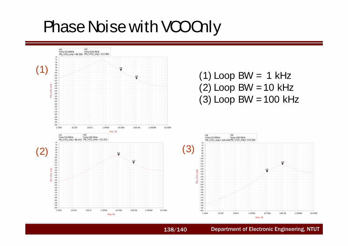
(1)
(2) (3)
m1freq=10.00kHzPN_VCO_only=-126.536
m2freq=100.0kHzPN_VCO_only=-112.256
10.00 100.0 1.000k 10.00k 100.0k 1.000M1.000 10.00M
-195-190-185-180-175-170-165-160-155-150-145-140-135-130-125-120-115-110-105-100-95-90-85-80-75
-200
-70
freq, Hz
PN
_VC
O_o
nly m1
m2
m1freq=10.00kHzPN_VCO_only=-96.380
m2freq=100.0kHzPN_VCO_only=-112.580
10.00 100.0 1.000k 10.00k 100.0k 1.000M1.000 10.00M
-195-190-185-180-175-170-165-160-155-150-145-140-135-130-125-120-115-110-105-100-95-90-85-80-75
-200
-70
freq, Hz
PN
_VC
O_o
nly
m1
m2
m1freq=10.00kHzPN_VCO_only=-96.443
m2freq=100.0kHzPN_VCO_only=-112.315
10.00 100.0 1.000k 10.00k 100.0k 1.000M1.000 10.00M
-195-190-185-180-175-170-165-160-155-150-145-140-135-130-125-120-115-110-105-100-95-90-85-80-75
-200
-70
freq, Hz
PN
_VC
O_o
nly
m1
m2
(1) Loop BW = 1 kHz(2) Loop BW =10 kHz(3) Loop BW =100 kHz
Phase Noise with VCO Only
Department of Electronic Engineering, NTUT138/140

(1)
(2) (3)
m1freq=1.000kHzPNTotal=-75.603
m2freq=10.00kHzPNTotal=-78.205
m3freq=1.000kHzPN_VCO_only=-146.498
m4freq=10.00kHzPN_VCO_only=-126.536
10.00 100.0 1.000k 10.00k 100.0k 1.000M1.000 10.00M
-140
-120
-100
-80
-60
-40
-20
0
-160
20
f req, Hz
PNTo
tal
m1 m2
PN
_VC
O_o
nly
m3
m4P
N_V
CO
_Fre
eRun
m1freq=1.000kHzPNTotal=-70.960
m2freq=10.00kHzPNTotal=-93.347
m3freq=1.000kHzPN_VCO_only=-76.978
m4freq=10.00kHzPN_VCO_only=-96.380
10.00 100.0 1.000k 10.00k 100.0k 1.000M1.000 10.00M
-140
-120
-100
-80
-60
-40
-20
0
-160
20
f req, Hz
PN
Tot
al m1
m2PN
_VC
O_o
nly
m3
m4PN
_VC
O_F
reeR
un
m1freq=1.000kHzPNTotal=-75.282
m2freq=10.00kHzPNTotal=-76.852
m3freq=1.000kHzPN_VCO_only=-106.753
m4freq=10.00kHzPN_VCO_only=-96.443
10.00 100.0 1.000k 10.00k 100.0k 1.000M1.000 10.00M
-140
-120
-100
-80
-60
-40
-20
0
-160
20
f req, Hz
PNTo
tal
m1 m2
PN
_VC
O_o
nly
m3m4P
N_V
CO
_Fre
eRun
(1) Loop BW = 1 kHz(2) Loop BW =10 kHz(3) Loop BW =100 kHz
VCO in Loop vs. VCO Free-Running
Department of Electronic Engineering, NTUT139/140

(1) N = 2400
(2) N= 1400
m1freq=1.000kHzPNTotal=-75.282
m2freq=10.00kHzPNTotal=-76.852
m3freq=1.000kHzPN_VCO_only=-106.753
m4freq=10.00kHzPN_VCO_only=-96.443
10.00 100.0 1.000k 10.00k 100.0k 1.000M1.000 10.00M
-140
-120
-100
-80
-60
-40
-20
0
-160
20
f req, Hz
PNTo
tal
m1 m2
PN_V
CO
_onl
y
m3m4PN
_VC
O_F
reeR
un
m1freq=1.000kHzPNTotal=-83.041
m2freq=10.00kHzPNTotal=-83.673
m3freq=1.000kHzPN_VCO_only=-114.513
m4freq=10.00kHzPN_VCO_only=-103.265
10.00 100.0 1.000k 10.00k 100.0k 1.000M1.000 10.00M
-140
-120
-100
-80
-60
-40
-20
0
-160
20
f req, Hz
PN
Tota
l
m1 m2
PN_V
CO
_onl
y
m3
m4PN
_VC
O_F
reeR
un
Phase Noise with Various Modulus N
Department of Electronic Engineering, NTUT140/140
Top Related