


Languages
Pages
Legal

OPEN ACCESS
Resistance switching at the nanometre scale inamorphous carbonTo cite this article: Abu Sebastian et al 2011 New J. Phys. 13 013020
View the article online for updates and enhancements.
You may also likeMicrowave preparation of two-dimensionalfermionic spin mixturesB Peaudecerf, M Andia, M Brown et al.
-
Fundamental physical features of resonantspontaneous bremsstrahlung radiation ofultrarelativistic electrons on nuclei instrong laser fieldsS P Roshchupkin, A V Dubov, V V Dubovet al.
-
Diamond-based single-molecule magneticresonance spectroscopyJianming Cai, Fedor Jelezko, Martin BPlenio et al.
-
This content was downloaded from IP address 27.33.79.2 on 18/03/2022 at 19:39
T h e o p e n – a c c e s s j o u r n a l f o r p h y s i c s
New Journal of Physics
Resistance switching at the nanometre scale inamorphous carbon
Abu Sebastian1,5, Andrew Pauza2, Christophe Rossel1,Robert M Shelby3, Arantxa Fraile Rodríguez4,6,Haralampos Pozidis1 and Evangelos Eleftheriou1
1 IBM Research—Zurich, 8803 Rüschlikon, Switzerland2 Plarion Limited, Melbourn Science Park, Melbourn, Herts SG8 6HB, UK3 IBM Research—Almaden, 650 Harry Road, San Jose, CA 95120, USA4 Swiss Light Source, Paul Scherrer Institut, 5232 Villigen PSI, SwitzerlandE-mail: [email protected]
New Journal of Physics 13 (2011) 013020 (12pp)Received 23 September 2010Published 14 January 2011Online at http://www.njp.org/doi:10.1088/1367-2630/13/1/013020
Abstract. The electrical transport and resistance switching mechanism inamorphous carbon (a-C) is investigated at the nanoscale. The electricalconduction in a-C thin films is shown to be captured well by a Poole–Frenkeltransport model that involves nonisolated traps. Moreover, at high electric fieldsa field-induced threshold switching phenomenon is observed. The followingresistance change is attributed to Joule heating and subsequent localized thermalannealing. We demonstrate that the mechanism is mostly due to clustering ofthe existing sp2 sites within the sp3 matrix. The electrical conduction behaviour,field-induced switching and Joule-heating-induced rearrangement of atomicorder resulting in a resistance change are all reminiscent of conventional phase-change memory materials. This suggests the potential of a-C as a similarnonvolatile memory candidate material.
5 Author to whom any correspondence should be addressed.6 Currently at Departament de Física Fonamental and Institut de Nanociència i Nanotecnologia (IN2UB),Universitat de Barcelona, 08028 Barcelona, Spain.
New Journal of Physics 13 (2011) 0130201367-2630/11/013020+12$33.00 © IOP Publishing Ltd and Deutsche Physikalische Gesellschaft
2
Contents
1. Introduction 22. I–V measurements on thin-film stacks consisting of amorphous carbon (a-C) 33. Electrical transport in a-C 54. The permanent resistance-change mechanism in a-C 75. Large-scale resistance patterning 106. Conclusions 10Acknowledgments 11References 11
1. Introduction
Recently, much attention has been focused on the use of various forms of carbon, such as carbonnanotubes and graphene, for nonvolatile memory applications [1]–[3]. However, compared tothese forms of carbon, amorphous carbon (a-C) is particularly interesting given the ease withwhich it can be incorporated into the cell structure of the most promising nonvolatile memorytechnology, phase-change memory [4, 5]. In fact, in this paper we illustrate the remarkablesimilarity between the behaviour of a-C and conventional phase-change materials such asgermanium antimony telluride (GST).
Carbon exists in multiple forms, the most prominent being the sp2-dominated graphiticform with its low resistivity and the sp3-dominated diamond form with its high resistivity [6, 7].As-deposited a-C has a certain ratio of sp2 and sp3 carbon. Changing this ratio can significantlyinfluence the conduction behaviour of carbon. Even for the same sp3/sp2 ratio, clustering ofsp2 carbons can lead to enhanced conductivity. The potential for changing the conductivityof a-C at the nanoscale makes it a promising candidate for nonvolatile memory applications.Moreover, the elemental nature of carbon makes a memory device based on carbon scale tovery small feature sizes. The deposition techniques will be much simpler. Carbon-based memorydevices will be immune to compositional changes that typically plague phase-change memorymaterials. There is also potential for reduced resistance drift and high levels of data retention.The aforementioned characteristics, along with the high resilience of carbon to a variety ofstimuli, make it an attractive material for memory applications.
In previous studies, heat treatment has been shown to change the electrical propertiesof a-C. By performing bulk annealing, Takai et al [8] changed the structure and electronicproperties of a-C. They concluded that there is no substantial change in the sp3–sp2 ratio upto a temperature of 1100 ◦C and explained the reduction in resistance during heat treatmentat lower temperatures by the clustering of sp2 carbon. A similar study was conducted byFerrari et al [9] and, more recently, by Grierson et al [10]. The application of high electricfields has also been shown to introduce structural changes in a-C. By applying high electricfields locally using a scanning tunnelling microscope probe, Mercer et al [11] demonstratedthat graphitic nanostructures can be formed on amorphous tetrahedral diamond-like carbon.In these experiments, there is no significant current flowing through the sample and thegraphitic formation is assumed to be field induced. Using spatially resolved electron energy
New Journal of Physics 13 (2011) 013020 (http://www.njp.org/)
3
loss spectroscopy, they concluded that the nanostructures arise after an electric-field-inducedtransformation from predominantly fourfold- to threefold-coordinated carbon.
It has also been shown that the resistance of a-C can be altered by passing current throughthe material. While studying conduction processes in doped diamond-like carbon films, Ronninget al [12] observed a permanent change in resistance. This effect has also been observed by Liuet al [13] while designing antifuses, by Tsuchitani et al [14] while exploring carbon for probe-based data storage, and by Kostylev et al [15] while investigating carbon as a potential electrodematerial for phase-change memory cells. This means of changing the electrical resistance ofa-C is particularly interesting for memory applications. Recently, Kreupl et al [16] built asimplistic memory device with a-C and were able to vary the resistance by applying currentpulses. The device structure also allowed them to reversibly switch the material between a highand a low resistance state.
In spite of these studies, there is a lack of understanding of the resistance-changemechanism. First of all, given the electrothermal origin of this resistance change, it is essentialto establish whether it is field induced or thermally induced. There is also a need to establishwhether the mechanism is rehybridization or rearrangement of carbon atoms. Moreover, theseinvestigations have to be conducted at the scale of tens of nanometres that is appropriate formemory applications. Besides the resistance-change mechanism, the conduction mechanism ina-C films needs to be investigated further because it has significant ramifications for propertiessuch as resistance drift and programming voltage, which are critical for nonvolatile memoryapplications.
In this paper, we present a thorough investigation of the electrical transport and resistanceswitching in a-C films. Conductive-mode atomic force microscopy (c-AFM) on thin carbonfilms deposited on conductive bottom electrodes is used in this study. Using this local probetechnique, we can switch the resistance of a-C with a spatial resolution of tens of nanometres.c-AFM and our stack configuration also enable the study of the electrical transport mechanismin a-C films across the thickness of these films. Films of varying thickness of a-C and probeswith different diameters are employed for this. The effect of thermal annealing is investigatedby the application of laser pulses, as well as bulk annealing using rapid thermal annealers.Raman and near-edge x-ray absorption fine structure (NEXAFS) spectroscopy are employedto investigate the resistance-change mechanism. Moreover, the capability of c-AFM probesto pattern large surfaces resistively is demonstrated. This can be exploited for probe-basednano-manufacturing, nano-electronics and probe-based data storage.
2. I–V measurements on thin-film stacks consisting of amorphous carbon (a-C)
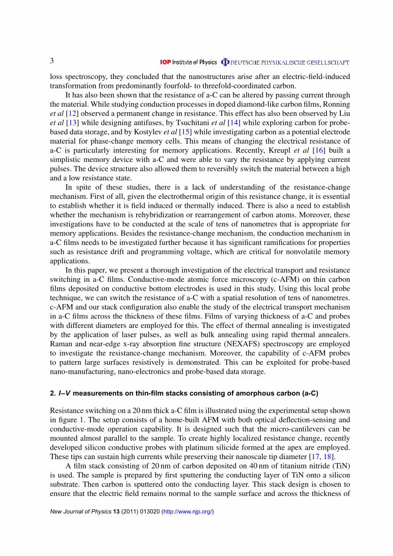
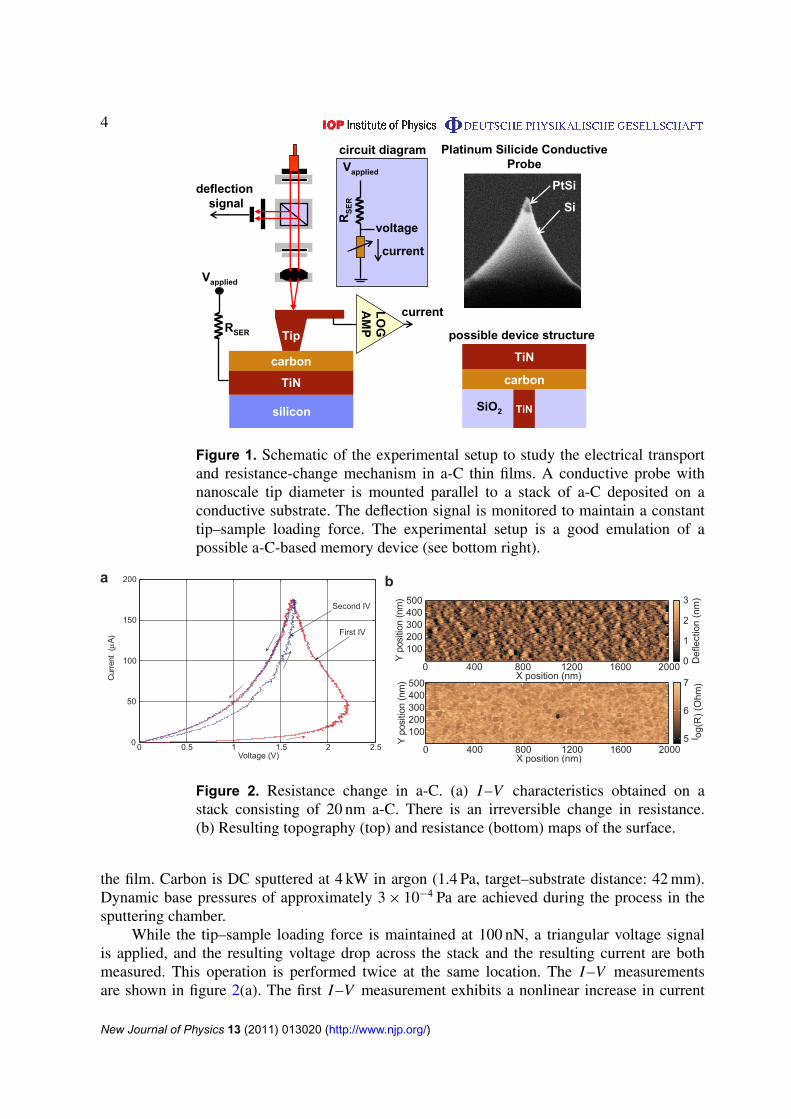
Resistance switching on a 20 nm thick a-C film is illustrated using the experimental setup shownin figure 1. The setup consists of a home-built AFM with both optical deflection-sensing andconductive-mode operation capability. It is designed such that the micro-cantilevers can bemounted almost parallel to the sample. To create highly localized resistance change, recentlydeveloped silicon conductive probes with platinum silicide formed at the apex are employed.These tips can sustain high currents while preserving their nanoscale tip diameter [17, 18].
A film stack consisting of 20 nm of carbon deposited on 40 nm of titanium nitride (TiN)is used. The sample is prepared by first sputtering the conducting layer of TiN onto a siliconsubstrate. Then carbon is sputtered onto the conducting layer. This stack design is chosen toensure that the electric field remains normal to the sample surface and across the thickness of
New Journal of Physics 13 (2011) 013020 (http://www.njp.org/)
4
possible device structure R
SE
R
Vapplied
voltage
current
TiN
carbon
TiNSiO2
current
silicon
Tip
TiN
carbon
LO
GA
MP
Vapplied
RSER
deflection signal
PtSi
Si
circuit diagram Platinum Silicide Conductive Probe
Figure 1. Schematic of the experimental setup to study the electrical transportand resistance-change mechanism in a-C thin films. A conductive probe withnanoscale tip diameter is mounted parallel to a stack of a-C deposited on aconductive substrate. The deflection signal is monitored to maintain a constanttip–sample loading force. The experimental setup is a good emulation of apossible a-C-based memory device (see bottom right).
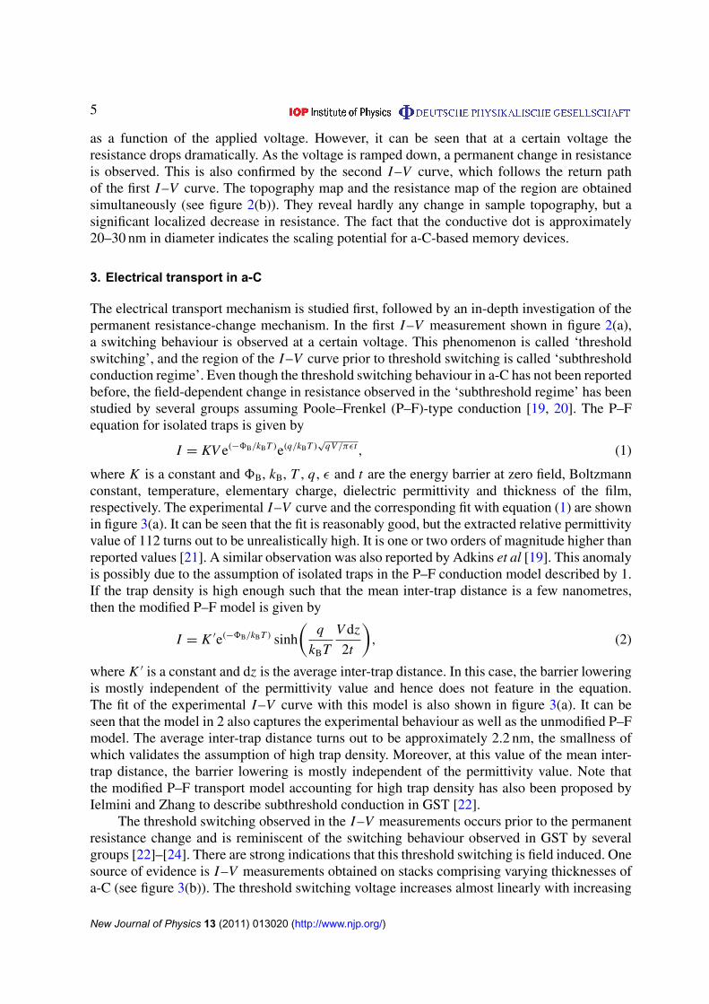
Figure 2. Resistance change in a-C. (a) I –V characteristics obtained on astack consisting of 20 nm a-C. There is an irreversible change in resistance.(b) Resulting topography (top) and resistance (bottom) maps of the surface.
the film. Carbon is DC sputtered at 4 kW in argon (1.4 Pa, target–substrate distance: 42 mm).Dynamic base pressures of approximately 3 × 10⁻⁴ Pa are achieved during the process in thesputtering chamber.
While the tip–sample loading force is maintained at 100 nN, a triangular voltage signalis applied, and the resulting voltage drop across the stack and the resulting current are bothmeasured. This operation is performed twice at the same location. The I –V measurementsare shown in figure 2(a). The first I –V measurement exhibits a nonlinear increase in current
New Journal of Physics 13 (2011) 013020 (http://www.njp.org/)
5
as a function of the applied voltage. However, it can be seen that at a certain voltage theresistance drops dramatically. As the voltage is ramped down, a permanent change in resistanceis observed. This is also confirmed by the second I –V curve, which follows the return pathof the first I –V curve. The topography map and the resistance map of the region are obtainedsimultaneously (see figure 2(b)). They reveal hardly any change in sample topography, but asignificant localized decrease in resistance. The fact that the conductive dot is approximately20–30 nm in diameter indicates the scaling potential for a-C-based memory devices.
3. Electrical transport in a-C
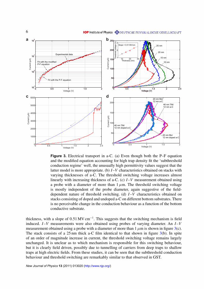
The electrical transport mechanism is studied first, followed by an in-depth investigation of thepermanent resistance-change mechanism. In the first I –V measurement shown in figure 2(a),a switching behaviour is observed at a certain voltage. This phenomenon is called ‘thresholdswitching’, and the region of the I –V curve prior to threshold switching is called ‘subthresholdconduction regime’. Even though the threshold switching behaviour in a-C has not been reportedbefore, the field-dependent change in resistance observed in the ‘subthreshold regime’ has beenstudied by several groups assuming Poole–Frenkel (P–F)-type conduction [19, 20]. The P–Fequation for isolated traps is given by
I = KV e(−8B/kBT )e(q/kBT )√
qV /πεt , (1)
where K is a constant and 8B, kB, T , q, ε and t are the energy barrier at zero field, Boltzmannconstant, temperature, elementary charge, dielectric permittivity and thickness of the film,respectively. The experimental I –V curve and the corresponding fit with equation (1) are shownin figure 3(a). It can be seen that the fit is reasonably good, but the extracted relative permittivityvalue of 112 turns out to be unrealistically high. It is one or two orders of magnitude higher thanreported values [21]. A similar observation was also reported by Adkins et al [19]. This anomalyis possibly due to the assumption of isolated traps in the P–F conduction model described by 1.If the trap density is high enough such that the mean inter-trap distance is a few nanometres,then the modified P–F model is given by
I = K ′e(−8B/kBT ) sinh
(q
kBT
V dz
2t
), (2)
where K ′ is a constant and dz is the average inter-trap distance. In this case, the barrier loweringis mostly independent of the permittivity value and hence does not feature in the equation.The fit of the experimental I –V curve with this model is also shown in figure 3(a). It can beseen that the model in 2 also captures the experimental behaviour as well as the unmodified P–Fmodel. The average inter-trap distance turns out to be approximately 2.2 nm, the smallness ofwhich validates the assumption of high trap density. Moreover, at this value of the mean inter-trap distance, the barrier lowering is mostly independent of the permittivity value. Note thatthe modified P–F transport model accounting for high trap density has also been proposed byIelmini and Zhang to describe subthreshold conduction in GST [22].
The threshold switching observed in the I –V measurements occurs prior to the permanentresistance change and is reminiscent of the switching behaviour observed in GST by severalgroups [22]–[24]. There are strong indications that this threshold switching is field induced. Onesource of evidence is I –V measurements obtained on stacks comprising varying thicknesses ofa-C (see figure 3(b)). The threshold switching voltage increases almost linearly with increasing
New Journal of Physics 13 (2011) 013020 (http://www.njp.org/)
6
0 0.5 1 1.5 210
-1
100
101
102
Voltage (V)
Cur
rent
( µA
)
0 0.5 1 1.5 210
-1
100
101
102
Cur
rent
( µA
)
0 0.5 1 1.5 2 2.50
50
100
150
200
250
Voltage (V)0 0.5 1 1.5 2 2.5
0
50
100
150
200
250
Voltage (V)
25 nm
20 nm
10 nm
10 nm 10 20 301
2
3
Thickness (nm)
Thr
esho
ldvo
l tage
(V)
Slope = 0.51 MV/cm
0 0.5 1 1.5 2 2.50
1000
2000
3000
4000
5000
6000
Voltage (V)
Cur
rent
( µA
)
0 0.5 1 1.5 20
50
100
150
200
Voltage (V)
20 nm Mo/ 12 nm a-C
40 nm TiN/ 12 nm a-C
Cur
rent
( µA
)
40 nm TiN/ 12 nm doped a-C
20 nm Mo/ 12 nm doped a-C
a b
c d
Fit with the modifiedP-F equation
Experimental data
Fit with the P-F equation
Figure 3. Electrical transport in a-C. (a) Even though both the P–F equationand the modified equation accounting for high trap density fit the ‘subthresholdconduction regime’ well, the unusually high permittivity values suggest that thelatter model is more appropriate. (b) I –V characteristics obtained on stacks withvarying thicknesses of a-C. The threshold switching voltage increases almostlinearly with increasing thickness of a-C. (c) I –V measurement obtained usinga probe with a diameter of more than 1 µm. The threshold switching voltageis mostly independent of the probe diameter, again suggestive of the field-dependent nature of threshold switching. (d) I –V characteristics obtained onstacks consisting of doped and undoped a-C on different bottom substrates. Thereis no perceivable change in the conduction behaviour as a function of the bottomconductive substrate.
thickness, with a slope of 0.51 MV cm−1. This suggests that the switching mechanism is fieldinduced. I –V measurements were also obtained using probes of varying diameter. An I –Vmeasurement obtained using a probe with a diameter of more than 1 µm is shown in figure 3(c).The stack consists of a 25 nm thick a-C film identical to that shown in figure 3(b). In spiteof an order of magnitude increase in current, the threshold switching voltage remains largelyunchanged. It is unclear as to which mechanism is responsible for this switching behaviour,but it is clearly field driven, possibly due to tunnelling of carriers from deep traps to shallowtraps at high electric fields. From these studies, it can be seen that the subthreshold conductionbehaviour and threshold switching are remarkably similar to that observed in GST.
New Journal of Physics 13 (2011) 013020 (http://www.njp.org/)
7
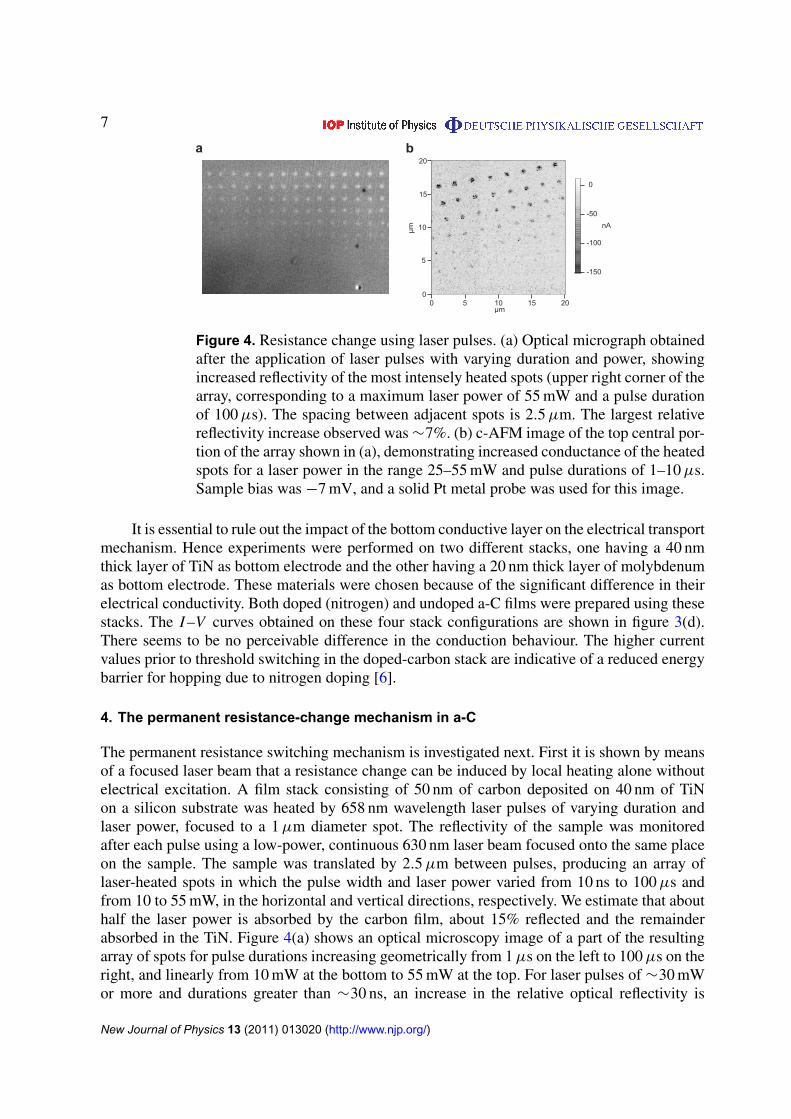
Figure 4. Resistance change using laser pulses. (a) Optical micrograph obtainedafter the application of laser pulses with varying duration and power, showingincreased reflectivity of the most intensely heated spots (upper right corner of thearray, corresponding to a maximum laser power of 55 mW and a pulse durationof 100 µs). The spacing between adjacent spots is 2.5 µm. The largest relativereflectivity increase observed was ∼7%. (b) c-AFM image of the top central por-tion of the array shown in (a), demonstrating increased conductance of the heatedspots for a laser power in the range 25–55 mW and pulse durations of 1–10 µs.Sample bias was −7 mV, and a solid Pt metal probe was used for this image.
It is essential to rule out the impact of the bottom conductive layer on the electrical transportmechanism. Hence experiments were performed on two different stacks, one having a 40 nmthick layer of TiN as bottom electrode and the other having a 20 nm thick layer of molybdenumas bottom electrode. These materials were chosen because of the significant difference in theirelectrical conductivity. Both doped (nitrogen) and undoped a-C films were prepared using thesestacks. The I –V curves obtained on these four stack configurations are shown in figure 3(d).There seems to be no perceivable difference in the conduction behaviour. The higher currentvalues prior to threshold switching in the doped-carbon stack are indicative of a reduced energybarrier for hopping due to nitrogen doping [6].
4. The permanent resistance-change mechanism in a-C
The permanent resistance switching mechanism is investigated next. First it is shown by meansof a focused laser beam that a resistance change can be induced by local heating alone withoutelectrical excitation. A film stack consisting of 50 nm of carbon deposited on 40 nm of TiNon a silicon substrate was heated by 658 nm wavelength laser pulses of varying duration andlaser power, focused to a 1 µm diameter spot. The reflectivity of the sample was monitoredafter each pulse using a low-power, continuous 630 nm laser beam focused onto the same placeon the sample. The sample was translated by 2.5 µm between pulses, producing an array oflaser-heated spots in which the pulse width and laser power varied from 10 ns to 100 µs andfrom 10 to 55 mW, in the horizontal and vertical directions, respectively. We estimate that abouthalf the laser power is absorbed by the carbon film, about 15% reflected and the remainderabsorbed in the TiN. Figure 4(a) shows an optical microscopy image of a part of the resultingarray of spots for pulse durations increasing geometrically from 1 µs on the left to 100 µs on theright, and linearly from 10 mW at the bottom to 55 mW at the top. For laser pulses of ∼30 mWor more and durations greater than ∼30 ns, an increase in the relative optical reflectivity is
New Journal of Physics 13 (2011) 013020 (http://www.njp.org/)
8
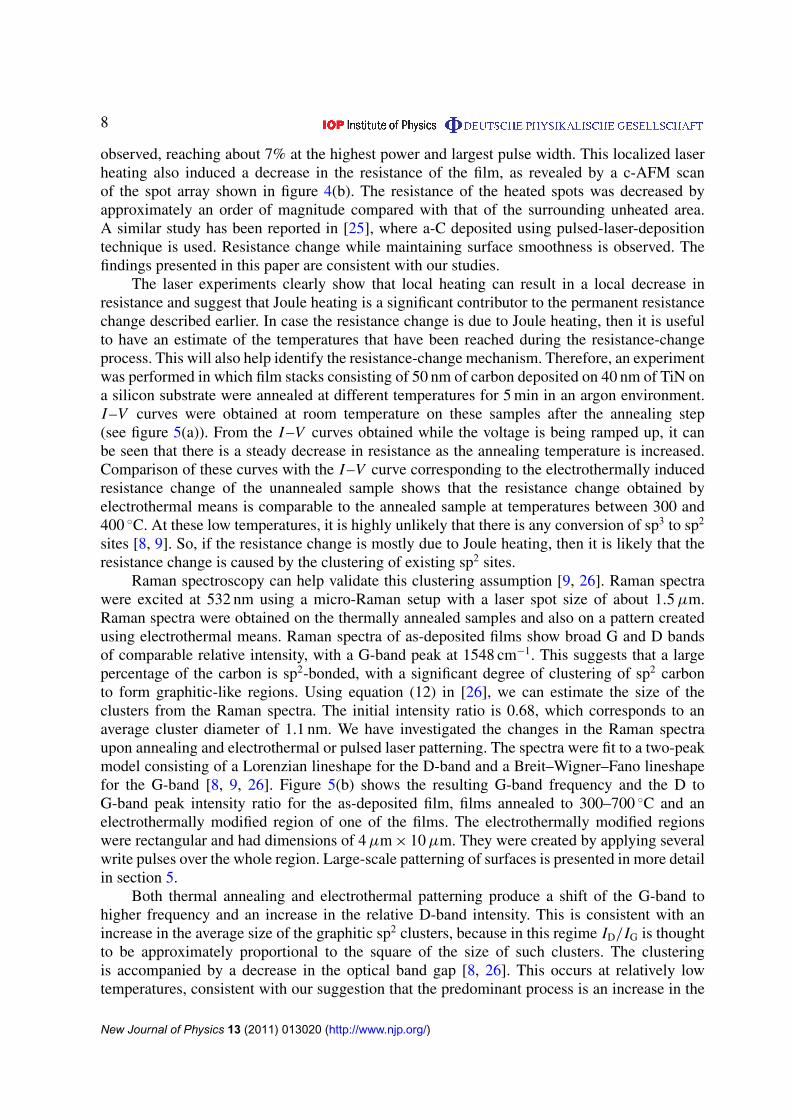
observed, reaching about 7% at the highest power and largest pulse width. This localized laserheating also induced a decrease in the resistance of the film, as revealed by a c-AFM scanof the spot array shown in figure 4(b). The resistance of the heated spots was decreased byapproximately an order of magnitude compared with that of the surrounding unheated area.A similar study has been reported in [25], where a-C deposited using pulsed-laser-depositiontechnique is used. Resistance change while maintaining surface smoothness is observed. Thefindings presented in this paper are consistent with our studies.
The laser experiments clearly show that local heating can result in a local decrease inresistance and suggest that Joule heating is a significant contributor to the permanent resistancechange described earlier. In case the resistance change is due to Joule heating, then it is usefulto have an estimate of the temperatures that have been reached during the resistance-changeprocess. This will also help identify the resistance-change mechanism. Therefore, an experimentwas performed in which film stacks consisting of 50 nm of carbon deposited on 40 nm of TiN ona silicon substrate were annealed at different temperatures for 5 min in an argon environment.I –V curves were obtained at room temperature on these samples after the annealing step(see figure 5(a)). From the I –V curves obtained while the voltage is being ramped up, it canbe seen that there is a steady decrease in resistance as the annealing temperature is increased.Comparison of these curves with the I –V curve corresponding to the electrothermally inducedresistance change of the unannealed sample shows that the resistance change obtained byelectrothermal means is comparable to the annealed sample at temperatures between 300 and400 ◦C. At these low temperatures, it is highly unlikely that there is any conversion of sp3 to sp2
sites [8, 9]. So, if the resistance change is mostly due to Joule heating, then it is likely that theresistance change is caused by the clustering of existing sp2 sites.
Raman spectroscopy can help validate this clustering assumption [9, 26]. Raman spectrawere excited at 532 nm using a micro-Raman setup with a laser spot size of about 1.5 µm.Raman spectra were obtained on the thermally annealed samples and also on a pattern createdusing electrothermal means. Raman spectra of as-deposited films show broad G and D bandsof comparable relative intensity, with a G-band peak at 1548 cm−1. This suggests that a largepercentage of the carbon is sp2-bonded, with a significant degree of clustering of sp2 carbonto form graphitic-like regions. Using equation (12) in [26], we can estimate the size of theclusters from the Raman spectra. The initial intensity ratio is 0.68, which corresponds to anaverage cluster diameter of 1.1 nm. We have investigated the changes in the Raman spectraupon annealing and electrothermal or pulsed laser patterning. The spectra were fit to a two-peakmodel consisting of a Lorenzian lineshape for the D-band and a Breit–Wigner–Fano lineshapefor the G-band [8, 9, 26]. Figure 5(b) shows the resulting G-band frequency and the D toG-band peak intensity ratio for the as-deposited film, films annealed to 300–700 ◦C and anelectrothermally modified region of one of the films. The electrothermally modified regionswere rectangular and had dimensions of 4 µm × 10 µm. They were created by applying severalwrite pulses over the whole region. Large-scale patterning of surfaces is presented in more detailin section 5.
Both thermal annealing and electrothermal patterning produce a shift of the G-band tohigher frequency and an increase in the relative D-band intensity. This is consistent with anincrease in the average size of the graphitic sp2 clusters, because in this regime ID/IG is thoughtto be approximately proportional to the square of the size of such clusters. The clusteringis accompanied by a decrease in the optical band gap [8, 26]. This occurs at relatively lowtemperatures, consistent with our suggestion that the predominant process is an increase in the
New Journal of Physics 13 (2011) 013020 (http://www.njp.org/)
9
b
c d
a
0 0.5 1 1.5 2 2.50
50
100
150
200
250
300
350
400
450
Voltage (V)
Cur
rent
(μA
)
500oC400oC 300oC
600oC
ETM Un-An.0.6
0.7
0.8
0.9
1
1.1
II D/II G
1540
1550
1560
1570
1580
VG
(cm
-1)
1540
1550
1560
1570
1580
400oC 500oC 600oC 700oC300oC
1000 1500 20000
1000
2000
3000
ν (cm-1)
Inte
nsity
(cou
nts)
GD
0 0.25 0.5 0.75 1 1.25 1.5 1.75 2 2.250
25
50
75
100
125
150
175
200
225
250
Voltage (V)
Cur
rent
( μA
)
280 285 290 295 300 305 310
0
0.2
0.4
0.6
0.8
1
Energy (eV)
Inte
nsity
(a.u
.)I n
ten s
i ty(a
.u.)
Modified surface
Unmodified surface
Un-An.
ETM
Unannealed
Increasing current
C 1s π*
C 1s σ*
Figure 5. The permanent resistance-change mechanism. (a) I –V curves obtainedat room temperature on annealed a-C stacks compared with an electrothermalswitching at room temperature. (b) Variation of G-band peak positions (squares)and ID/IG peak intensity ratios (circles) from the visible Raman spectraobtained from thermally annealed samples (300–700◦C), unannealed (Un-An.)and electrothermally modified (ETM) samples. In the inset, the Raman spectrumobtained from the electrothermally modified sample is compared with thatobtained from the unannealed sample. (c) I –V characteristics obtained withincreasing values of current on a stack consisting of 20 nm a-C. There is adirect correlation between the extent of resistance change and the applied power.(d) Comparison of the NEXAFS spectra of the a-C film inside and outside anelectrothermally modified area. The ratio of the areas under the C 1s → π∗ andC 1s → σ ∗ resonances remains largely unchanged.
average size of sp2 clusters rather than sp3 to sp2 conversion. The increase in ID/IG ratio andin the G-band peak position for the electrothermally modified sample similar in magnitude tothose for thermally annealed samples at 400–500 ◦C, which is remarkably close to the estimatefrom the I –V measurements presented earlier.
In figure 5(c), experimental results are presented in which resistance change is obtainedwith increasing current amplitudes. It can be seen that the extent of resistance change increaseswith increasing current and the corresponding increase in power. This is also suggestive of theresistance-change mechanism being induced by Joule heating. It has significant ramificationsfor multi-level storage in the context of memory applications.
New Journal of Physics 13 (2011) 013020 (http://www.njp.org/)
10
Given the electrothermal nature of resistance switching, there could be some sp3 to sp2
conversion due to the high fields that are generated within the carbon film. NEXAFS spectra ofthe as-deposited a-C film and the electrothermally modified surface were obtained to investigatethis possibility. The NEXAFS spectra were obtained using a photoemission electron microscope(PEEM) in ultra-high vacuum conditions. The laterally resolved NEXAFS experiments wereperformed at the surface/interface:microscopy beamline of the Swiss Light Source, using anElmitec PEEM equipped with an energy analyzer. Several NEXAFS spectra were obtainedinside and outside an electrothermally modified area and the average of these spectra is shownin figure 5(d). The peak at around 285.5 eV is due to the C 1s → π∗ transition for disorderedcarbon–carbon sp2-hybridized bonds and a broad peak starting above 288 eV and extendingup to 305 eV is due to the C 1s → σ ∗ transition for disordered carbon–carbon σ bonds. Thesimilarity between the two curves suggests that the sp3–sp2 ratio remains largely unchanged.The ratio of the area under the C 1s → π∗ and C 1s → σ ∗ resonances would have changedsignificantly if there was a change in the sp3–sp2 ratio [10]. Hence from all these results, it isestablished that the resistance change is caused by Joule-heating-induced clustering of existingsp2 sites, or in other words the rearrangement of sp2 carbon atoms within the sp3 matrix, asopposed to any significant rehybridization of the carbon atoms.
5. Large-scale resistance patterning
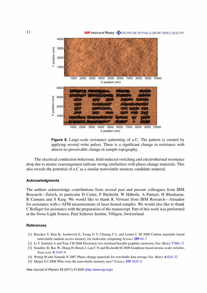
Besides memory applications, the capability of conductive probes to create highly localizedresistance change on a-C thin films can be exploited for applications such as probe-basednano-manufacturing, nano-electronics and probe-based data storage [27]–[30]. To study thepotential for large-scale resistance patterning at the nanoscale, a large pattern consisting ofapproximately 5000 write pulses was written using the platinum silicide conductive probes ona stack consisting of 50 nm of carbon film on 40 nm of TiN. The resulting topography andconduction maps are shown in figure 6. It can be seen that there is no appreciable change in thesample topography; however, there is a significant change in resistance. This experiment clearlydemonstrates the capability of conductive probes to resistively pattern large areas of a-C filmswith high throughput.
6. Conclusions
The electrical transport and resistance-change mechanisms in thin a-C films are investigated.It is demonstrated that we can locally switch the resistance of these films down to tens ofnanometres using c-AFM probes. Newly developed platinum silicide conductive probes whichcan sustain high currents while maintaining a small tip diameter were employed.
A P–F-type transport model that accounts for nonisolated traps describes the electricaltransport up to a certain electric field well, at which point there is evidence of a thresholdswitching behaviour. This results in a significant increase in the current flowing through thesample and subsequent Joule heating, which results in a permanent resistance drop. Thethermal origins of this resistance change are firmly established by laser-pulse-induced resistancepatterning and bulk annealing studies. Raman spectroscopy and NEXAFS spectroscopy allowus to conclude that the resistance change is caused by the clustering of existing sp2 sites withinthe sp3 matrix.
New Journal of Physics 13 (2011) 013020 (http://www.njp.org/)
11
12
X position (nm)
Y p
ositi
on (
nm)
1000 2000 3000 4000 5000 6000 7000 8000 9000 10000
1000
2000
3000
4000
X position (nm)
Y p
ositi
on (
nm)
1000 2000 3000 4000 5000 6000 7000 8000 9000 10000
1000
2000
3000
4000
Figure 6. Large-scale resistance patterning of a-C. The pattern is created byapplying several write pulses. There is a significant change in resistance withalmost no perceivable change in sample topography.
The electrical conduction behaviour, field-induced switching and electrothermal resistancedrop due to atomic rearrangement indicate strong similarities with phase-change materials. Thisalso reveals the potential of a-C as a similar nonvolatile memory candidate material.
Acknowledgments
The authors acknowledge contributions from several past and present colleagues from IBMResearch—Zurich, in particular D Caimi, P Bächtold, W Häberle, A Pantazi, H Bhaskaran,R Cannara and S Karg. We would like to thank K Virwani from IBM Research—Almadenfor assistance with c-AFM measurements of laser-heated samples. We would also like to thankC Bolliger for assistance with the preparation of the manuscript. Part of this work was performedat the Swiss Light Source, Paul Scherrer Institut, Villigen, Switzerland.
References
[1] Rueckes T, Kim K, Joselevich E, Tseng G Y, Cheung C-L and Lieber C M 2000 Carbon nanotube basednonvolatile random access memory for molecular computing Science 289 94–7
[2] Li Y, Sinitskii A and Tour J M 2008 Electronic two-terminal bistable graphitic memories Nat. Mater. 7 966–71[3] Standley B, Bao W, Zhang H, Bruck J, Lau C N and Bockrath M 2008 Graphene-based atomic-scale switches
Nano Lett. 8 3345–9[4] Wuttig M and Yamada N 2007 Phase-change materials for rewritable data storage Nat. Mater. 6 824–32[5] Meijer G I 2008 Who wins the nonvolatile memory race? Science 319 1625–6
New Journal of Physics 13 (2011) 013020 (http://www.njp.org/)
12
[6] Robertson J 2002 Diamond-like amorphous carbon Mater. Sci. Eng. 37 129–81[7] Silva S R P 2003 Properties of Amorphous Carbon 1st edn (Stevenage: The Institution of Engineering and
Technology)[8] Takai K, Oga M, Sato H, Enoki T, Ohki Y, Taomoto A, Suenaga K and Iijima S 2003 Structure and electronic
properties of a nongraphitic disordered carbon system and its heat-treatment effects Phys. Rev. B 67 214202[9] Ferrari A C, Kleinsorge B, Morrison N A, Hart A, Stolojan V and Robertson J 1999 Stress reduction and
bond stability during thermal annealing of tetrahedral amorphous carbon J. Appl. Phys. 85 7191–7[10] Grierson D S, Sumant A V, Konicek A R, Friedmann T A, Sullivan J P and Carpick R W 2010 Thermal
stability and rehybridization of carbon bonding in tetrahedral amorphous carbon J. Appl. Phys. 107 033523[11] Mercer T W, DiNardo N J, Rothman J B, Siegal M P, Friedmann T A and Martinez-Miranda L J 1998 Electron
emission induced modifications in amorphous tetrahedral diamondlike carbon Appl. Phys. Lett. 72 2244–6[12] Ronning C, Griesmeier U, Gross M, Hoffsäss H C, Downing R G and Lamaze G P 1995 Conduction processes
in boron-nitrogen-doped diamond-like carbon films prepared by mass-separated ion beam deposition Diam.Relat. Mater. 4 666–72
[13] Liu S, Lamp D, Gangopadhyay S, Sreenivas G, Ang S S and Naseem H A 1998 A new metal-to-metal antifusewith amorphous carbon IEEE Electron Device Lett. 19 317
[14] Tsuchitani S, Isozaki M, Kaneko R, Tanaka I and Hirono S 2004 Nanometer-scale recording on a superhardand conductive carbon film using an atomic force microscope Japan. J. Appl. Phys. 43 7677–81
[15] Kostylev S, Lowrey T and Czubatyj W 2007 Programming speed in ovonic unified memory Proc. of theEuropean Phase Change and Ovonics Symp.
[16] Kreupl F et al 2008 Carbon-based resistive memory IEEE Int. Electron Devices Meeting Technical Digestpp 521–4
[17] Bhaskaran H, Sebastian A and Despont M 2009 Nanoscale PtSi tips for conducting probe technologies IEEETrans. Nanotechnol. 8 128–31
[18] Bhaskaran H, Sebastian A, Pauza A, Pozidis H and Despont M 2009 Nanoscale phase transformationin Ge2Sb2Te5 using encapsulated scanning probes and retraction force microscopy Rev. Sci. Instrum.80 083701
[19] Adkins C J, Freake S M and Hamilton E M 1970 Electrical conduction in amorphous carbon Phil. Mag.22 183–8
[20] Khan R U A and Silva S R P 2000 Electronic conduction in ion implanted amorphous carbon thin filmsInt. J. Mod. Phys. B 14 195–2005
[21] Balachova O V, Swart J W, Braga E S and Cescato L 2001 Permittivity of amorphous hydrogenated carbon(a-C:H) films as a function of thermal annealing Microelectron. J. 32 673–8
[22] Ielmini D and Zhang Y 2007 Analytical model for subthreshold conduction and threshold switching inchalcogenide-based memory devices J. Appl. Phys. 102 054517
[23] Adler D, Shur M S, Silver M and Ovshinsky S R 1980 Threshold switching in chalcogenide-glass thin filmsJ. Appl. Phys. 51 3289–309
[24] Pirovano A, Lacaita A L, Benvenuti A, Pellizer F and Bez R 2004 Electronic switching in phase-changememories IEEE Trans. Electron. Devices 51 452–9
[25] Miyajima Y, Adikaari A A D T, Henley S J, Shannon J M and Silva S R P 2008 Electrical properties of pulsedUV laser irradiated amorphous carbon Appl. Phys. Lett. 92 152104
[26] Ferrari A C and Robertson J 2000 Interpretation of Raman spectra of disordered and amorphous carbonPhys. Rev. B 61 14095
[27] Pires D, Hedrick J L, Silva De A, Frommer J, Gotsmann B, Wolf H, Despont M, Duerig U and Knoll A W2010 Nanoscale three-dimensional patterning of molecular resists by scanning probes Science 328 732–5
[28] Guisinger N P and Arnold M S 2010 Beyond silicon: carbon-based nanotechnology MRS Bull. 35 273–9[29] Wright C D, Shah P, Wang L, Aziz M M, Sebastian A and Pozidis H 2010 Write strategies for multiterabit
per square inch scanned-probe phase-change memories Appl. Phys. Lett. 97 173104[30] Pantazi A et al 2008 Probe-based ultrahigh-density storage technology IBM J. Res. Dev. 52 493–511
New Journal of Physics 13 (2011) 013020 (http://www.njp.org/)