


Languages
Pages
Legal

COP820CJ
Application Note 953 LCD Triplex Drive with COP820CJ
Literature Number: SNOA329
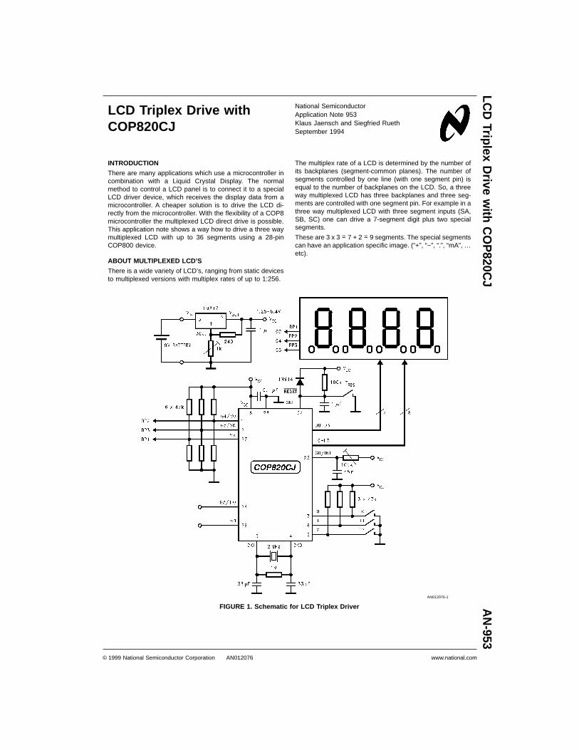
LCD Triplex Drive withCOP820CJ
INTRODUCTION
There are many applications which use a microcontroller incombination with a Liquid Crystal Display. The normalmethod to control a LCD panel is to connect it to a specialLCD driver device, which receives the display data from amicrocontroller. A cheaper solution is to drive the LCD di-rectly from the microcontroller. With the flexibility of a COP8microcontroller the multiplexed LCD direct drive is possible.This application note shows a way how to drive a three waymultiplexed LCD with up to 36 segments using a 28-pinCOP800 device.
ABOUT MULTIPLEXED LCD’S
There is a wide variety of LCD’s, ranging from static devicesto multiplexed versions with multiplex rates of up to 1:256.
The multiplex rate of a LCD is determined by the number ofits backplanes (segment-common planes). The number ofsegments controlled by one line (with one segment pin) isequal to the number of backplanes on the LCD. So, a threeway multiplexed LCD has three backplanes and three seg-ments are controlled with one segment pin. For example in athree way multiplexed LCD with three segment inputs (SA,SB, SC) one can drive a 7-segment digit plus two specialsegments.
These are 3 x 3 = 7 + 2 = 9 segments. The special segmentscan have an application specific image. (“+”, “−”, “.”, “mA”, …etc).
AN012076-1
FIGURE 1. Schematic for LCD Triplex Driver
National SemiconductorApplication Note 953Klaus Jaensch and Siegfried RuethSeptember 1994
LCD
TriplexD
rivew
ithC
OP
820CJ
AN
-953
© 1999 National Semiconductor Corporation AN012076 www.national.com
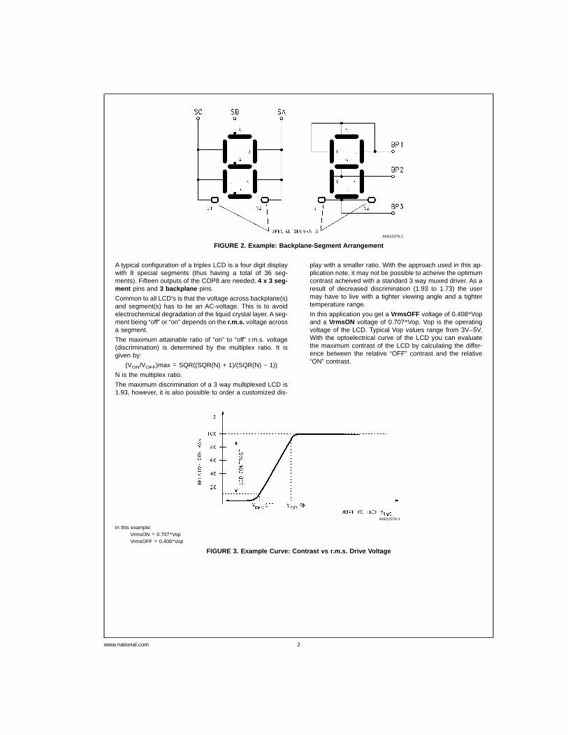
A typical configuration of a triplex LCD is a four digit displaywith 8 special segments (thus having a total of 36 seg-ments). Fifteen outputs of the COP8 are needed; 4 x 3 seg-ment pins and 3 backplane pins.
Common to all LCD’s is that the voltage across backplane(s)and segment(s) has to be an AC-voltage. This is to avoidelectrochemical degradation of the liquid crystal layer. A seg-ment being “off” or “on” depends on the r.m.s. voltage acrossa segment.
The maximum attainable ratio of “on” to “off” r.m.s. voltage(discrimination) is determined by the multiplex ratio. It isgiven by:
(VON/VOFF)max = SQR((SQR(N) + 1)/(SQR(N) − 1))
N is the multiplex ratio.
The maximum discrimination of a 3 way multiplexed LCD is1.93, however, it is also possible to order a customized dis-
play with a smaller ratio. With the approach used in this ap-plication note, it may not be possible to acheive the optimumcontrast acheived with a standard 3 way muxed driver. As aresult of decreased discrimination (1.93 to 1.73) the usermay have to live with a tighter viewing angle and a tightertemperature range.
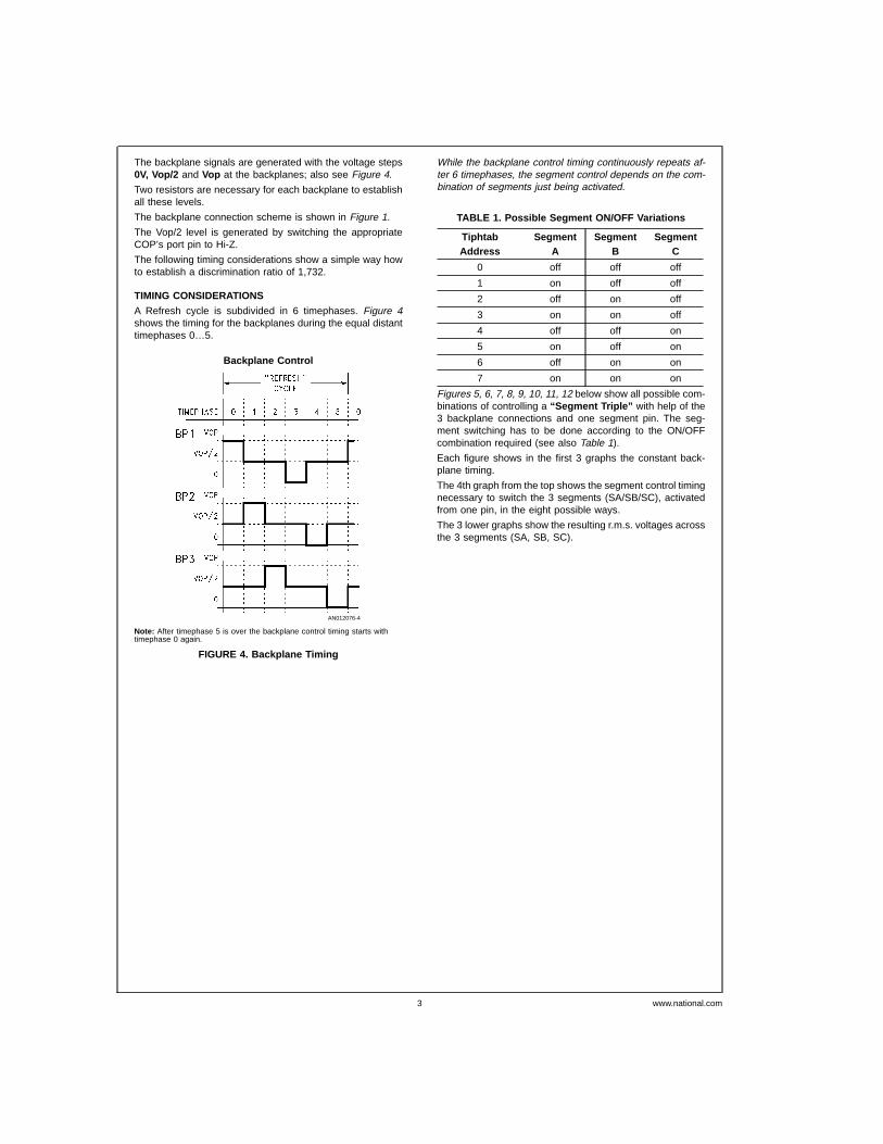
In this application you get a VrmsOFF voltage of 0.408*Vopand a VrmsON voltage of 0.707*Vop. Vop is the operatingvoltage of the LCD. Typical Vop values range from 3V–5V.With the optoelectrical curve of the LCD you can evaluatethe maximum contrast of the LCD by calculating the differ-ence between the relative “OFF” contrast and the relative“ON” contrast.
AN012076-2
FIGURE 2. Example: Backplane-Segment Arrangement
AN012076-3
In this example:VrmsON = 0.707*VopVrmsOFF = 0.408*Vop
FIGURE 3. Example Curve: Contrast vs r.m.s. Drive Voltage
www.national.com 2
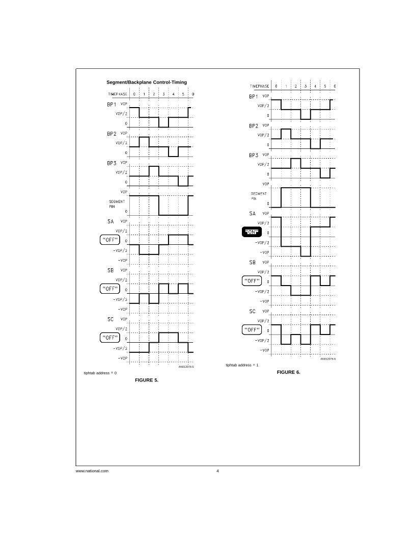
The backplane signals are generated with the voltage steps0V, Vop/2 and Vop at the backplanes; also see Figure 4.
Two resistors are necessary for each backplane to establishall these levels.
The backplane connection scheme is shown in Figure 1.
The Vop/2 level is generated by switching the appropriateCOP’s port pin to Hi-Z.
The following timing considerations show a simple way howto establish a discrimination ratio of 1,732.
TIMING CONSIDERATIONS
A Refresh cycle is subdivided in 6 timephases. Figure 4shows the timing for the backplanes during the equal distanttimephases 0…5.
While the backplane control timing continuously repeats af-ter 6 timephases, the segment control depends on the com-bination of segments just being activated.
TABLE 1. Possible Segment ON/OFF Variations
TiphtabAddress
SegmentA
SegmentB
SegmentC
0 off off off
1 on off off
2 off on off
3 on on off
4 off off on
5 on off on
6 off on on
7 on on on
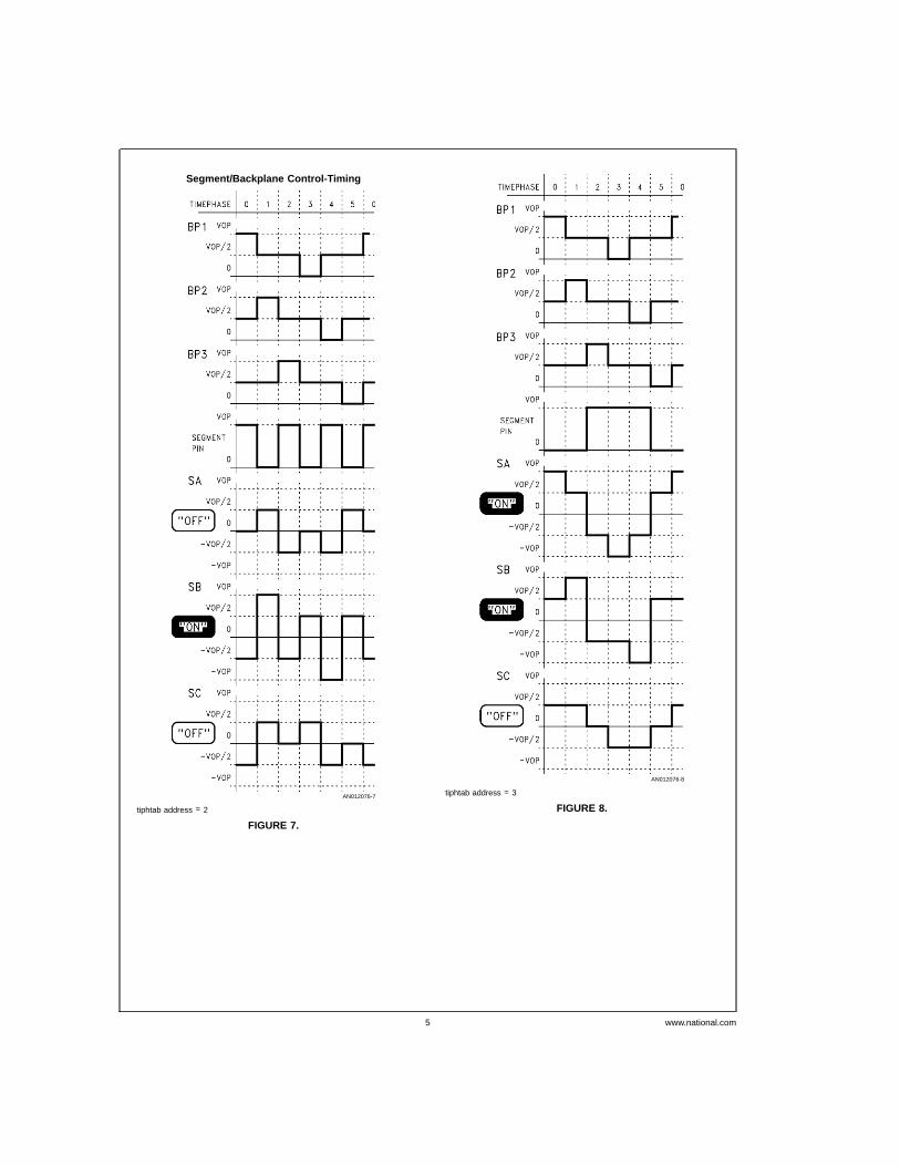
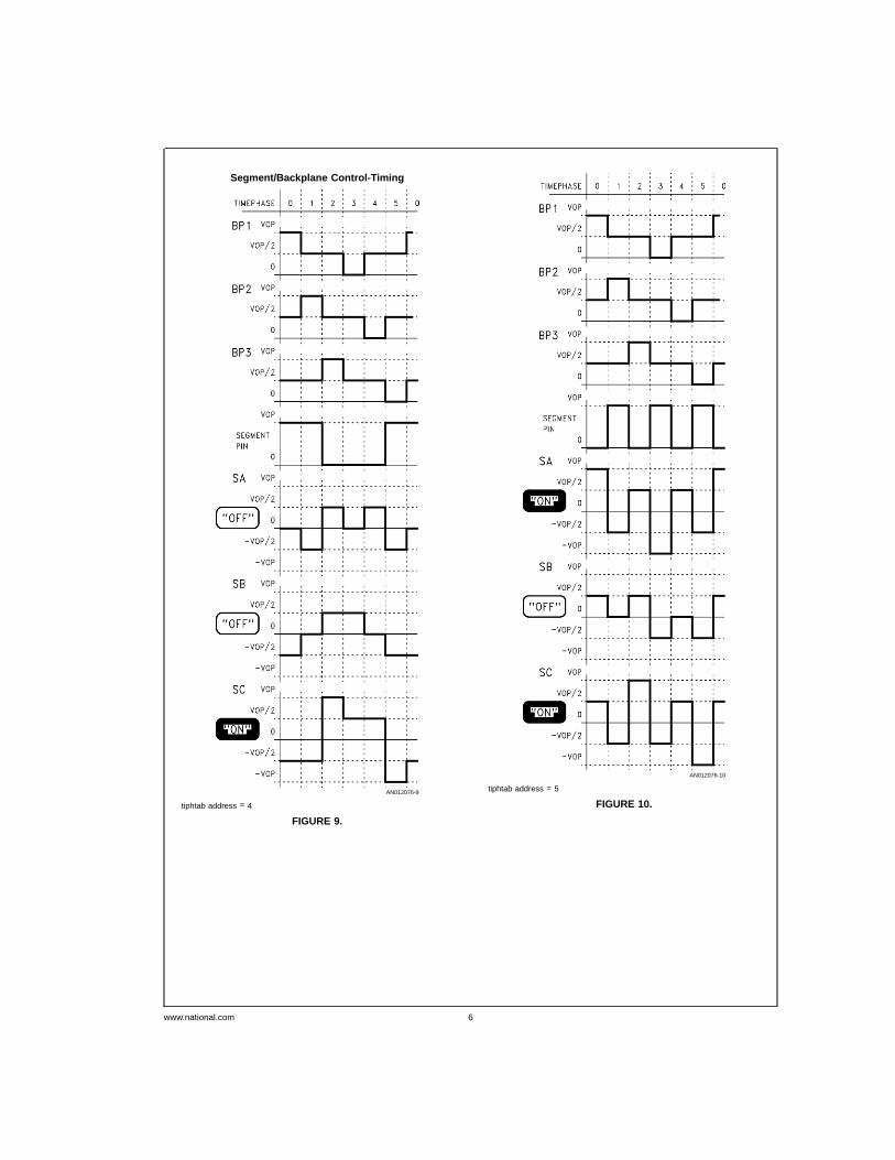
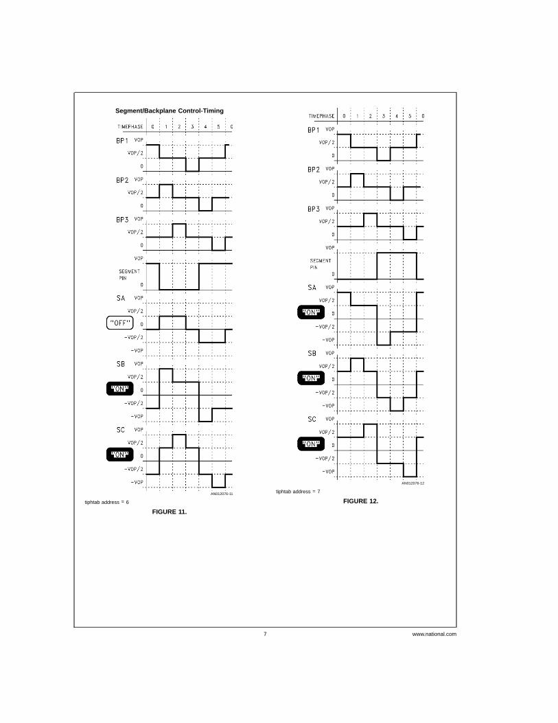
Figures 5, 6, 7, 8, 9, 10, 11, 12 below show all possible com-binations of controlling a “Segment Triple” with help of the3 backplane connections and one segment pin. The seg-ment switching has to be done according to the ON/OFFcombination required (see also Table 1).
Each figure shows in the first 3 graphs the constant back-plane timing.
The 4th graph from the top shows the segment control timingnecessary to switch the 3 segments (SA/SB/SC), activatedfrom one pin, in the eight possible ways.
The 3 lower graphs show the resulting r.m.s. voltages acrossthe 3 segments (SA, SB, SC).
Backplane Control
AN012076-4
Note: After timephase 5 is over the backplane control timing starts withtimephase 0 again.
FIGURE 4. Backplane Timing
www.national.com3
Segment/Backplane Control-Timing
AN012076-5
tiphtab address = 0
FIGURE 5.
AN012076-6
tiphtab address = 1
FIGURE 6.
www.national.com 4
Segment/Backplane Control-Timing
AN012076-7
tiphtab address = 2
FIGURE 7.
AN012076-8
tiphtab address = 3
FIGURE 8.
www.national.com5
Segment/Backplane Control-Timing
AN012076-9
tiphtab address = 4
FIGURE 9.
AN012076-10
tiphtab address = 5
FIGURE 10.
www.national.com 6
Segment/Backplane Control-Timing
AN012076-11
tiphtab address = 6
FIGURE 11.
AN012076-12
tiphtab address = 7
FIGURE 12.
www.national.com7
REFRESH FREQUENCY
One period with six timephases is called a refresh cycle(also see Figure 4).
The refresh cycle should be in a frequency range of 30…60Hz. A frequency below 30 Hz will cause a flickering display.On the other hand, current consumption increases with theLCD’s frequency. So it is also recommended to choose a fre-quency below 60 Hz.
In order to periodically update the µC’s port pins (involved inbackplane or segment control) at the beginning of a newtimephase, the COP8 needs a timebase of typ. 4 ms which isrealized with an external RC-circuit at the G0/INT pin.
The G0 pin is programmable as input (Schmitt Trigger). Theconditions for the external interrupt could be set for a low tohigh transition on the G0 pin setting the IPND-flag (externalinterrupt pending flag) upon an occurrence of such a transi-tion. The external capacitor can be discharged, with the G0pin configured as Push/Pull output and programmed to “0”.When, switching G0 as input the Cap. will be chargedthrough the resistor, until the threshold voltage of theSchmitt-Trigger input is reached. This triggers the externalinterrupt. The first thing the interrupt service routine has todo is to discharge the capacitor and switch G0 as input to re-start the procedure.
This timing method has the advantage, that the timer of thedevice is free for other tasks (for example to do an A/D con-version).
The time interval between two interrupts depends on the RCcircuit and the threshold of the G0 Schmitt Trigger VTH.
The refresh frequency is independent of the clock frequencyprovided to the COPs device.
The variations of “threshold” levels relative to VCC (over pro-cess) are as follows:
(VTH /VCC) min = 0.376
(VTH /VCC) max = 0.572
at VCC = 5V
Charge Time:
T = −(ln(1-VTH/VCC)*RC)
To prevent a flickering display one should aim at a minimumrefresh frequency of frefr = 30 Hz. This means an interruptfrequency of fint = 6 x 30 Hz = 180 Hz. So, the maximumcharge up time Tmax must not exceed 5.5 ms (Tmin =2.78 ms).
With the formula:
RCmax =Tmax/(−In(1−(VTH/VCC)max)) =5.5 msx0.849
RCmax = 6.48 ms
(RCmin = 5.98 ms)
The maximum RC time-constant is calculated. The minimumRC time constant can be calculated similarly.
A capacitor in the nF-range should be used (e.g. 68 nF), be-cause a bigger one needs too much time to discharge. Todischarge a 68 nF Cap., the G0 pin of the device has to below for about 40 µs.
On the other hand the capacitor should be large enough toreduce noise susceptibility.
When the RC combination is chosen, one can calculate themaximum refresh frequency by using the minimum values ofthe RC constant and the minimum threshold voltage:
Tmin =RCmin *(−In(1−(VTH/VCC)min)) =RCmin *0.472
and
frefr,max = fint,max /6 = 1/(Tmin *6)
In the above example one timephase would be minimum2.82 ms long. This means that about 250 instructions couldbe executed during this time.
SOFTWARE
The software for the triplex LCD drive-demo is composed ofthree parts:
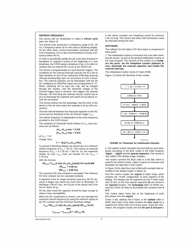
1. The initialization routine is executed only once after reset-ting the device, as part of the general initialization routine ofthe main program. The function of this routine is to config-ure the ports, set the timephase counter (tiphase) tozero, discharge the external capacitor and enable theexternal interrupt.
The initialization routine needs 37 bytes ROM.
Figure 13 shows the flowchart of this routine.
2. The update routine calculates the port-data for each time-phase according to the BCD codes in the RAM locations‘digit1’… ‘digit4’ and the special segments . This routine isonly called if the display image changes.
The routine converts the BCD code to a list 1st , which isused by the refresh routine. Figure 14 gives an overview andillustrates the data flow in this routine.
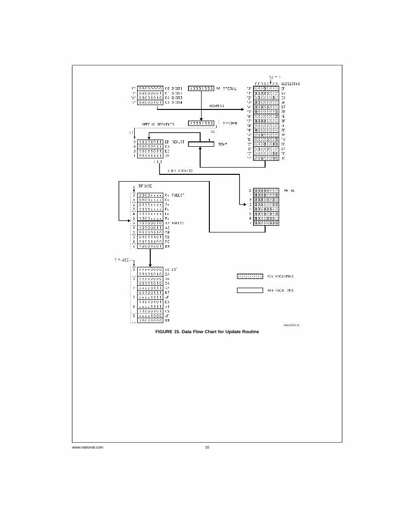
In Figure 15 the data flow chart is filled with example data ac-cording to the display image in Figure 16.
First the routine creates the seg1st (4 bytes long), whichcontains the “on/off” configuration of each segment of thedisplay. The display has 36 segments but the 4 bytes haveonly 32 bits, so the four special segments S1 are stored inthe specbuf location. The bcdsegtab table (in ROM) con-tains the LOOK-UP data for all possible Hex numbers from 0to F .
The routine takes three bits at the beginning of eachtime-phase from the seg1st .
These 3 bits address the 8 bytes of the tiphtab table inROM. Each byte of this table contains the time curve for asegment pin (only 6 bits out of 8 are used). Using this infor-mation, the program creates the lists for port D and port L
AN012076-13
FIGURE 13. Flowchart for Initialization Routine
www.national.com 8
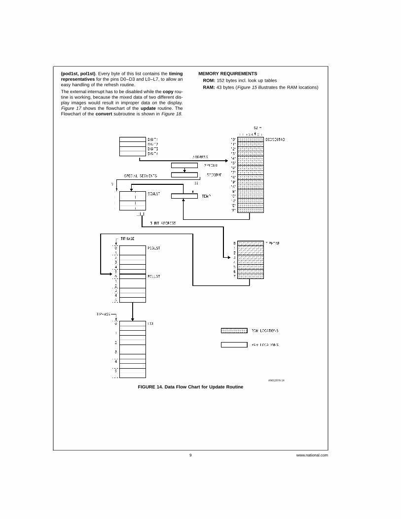
(pod1st, pol1st) . Every byte of this list contains the timingrepresentatives for the pins D0–D3 and L0–L7, to allow aneasy handling of the refresh routine.
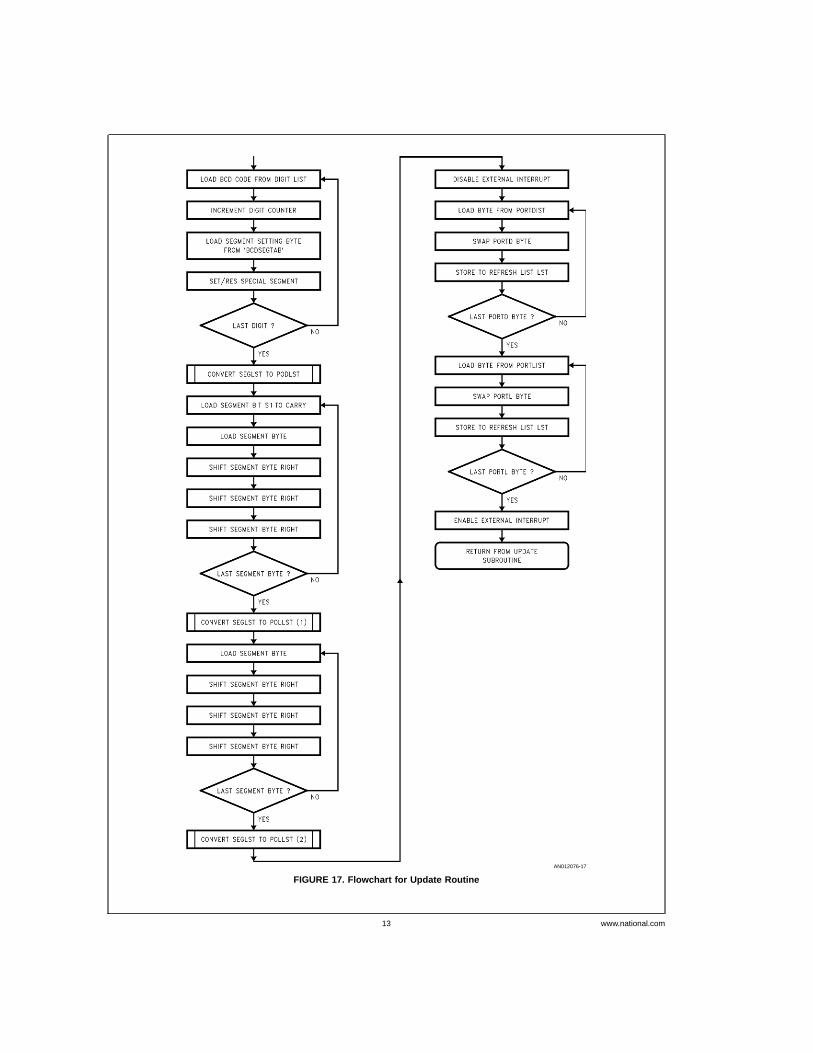
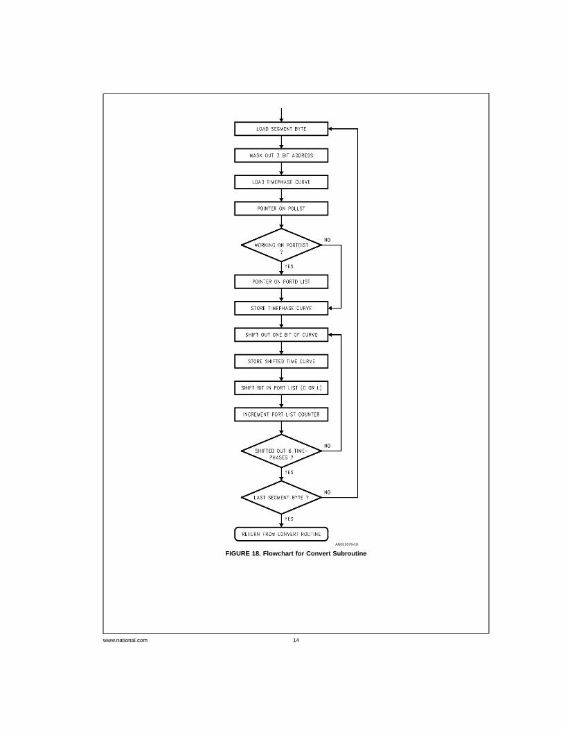
The external interrupt has to be disabled while the copy rou-tine is working, because the mixed data of two different dis-play images would result in improper data on the display.Figure 17 shows the flowchart of the update routine. TheFlowchart of the convert subroutine is shown in Figure 18.
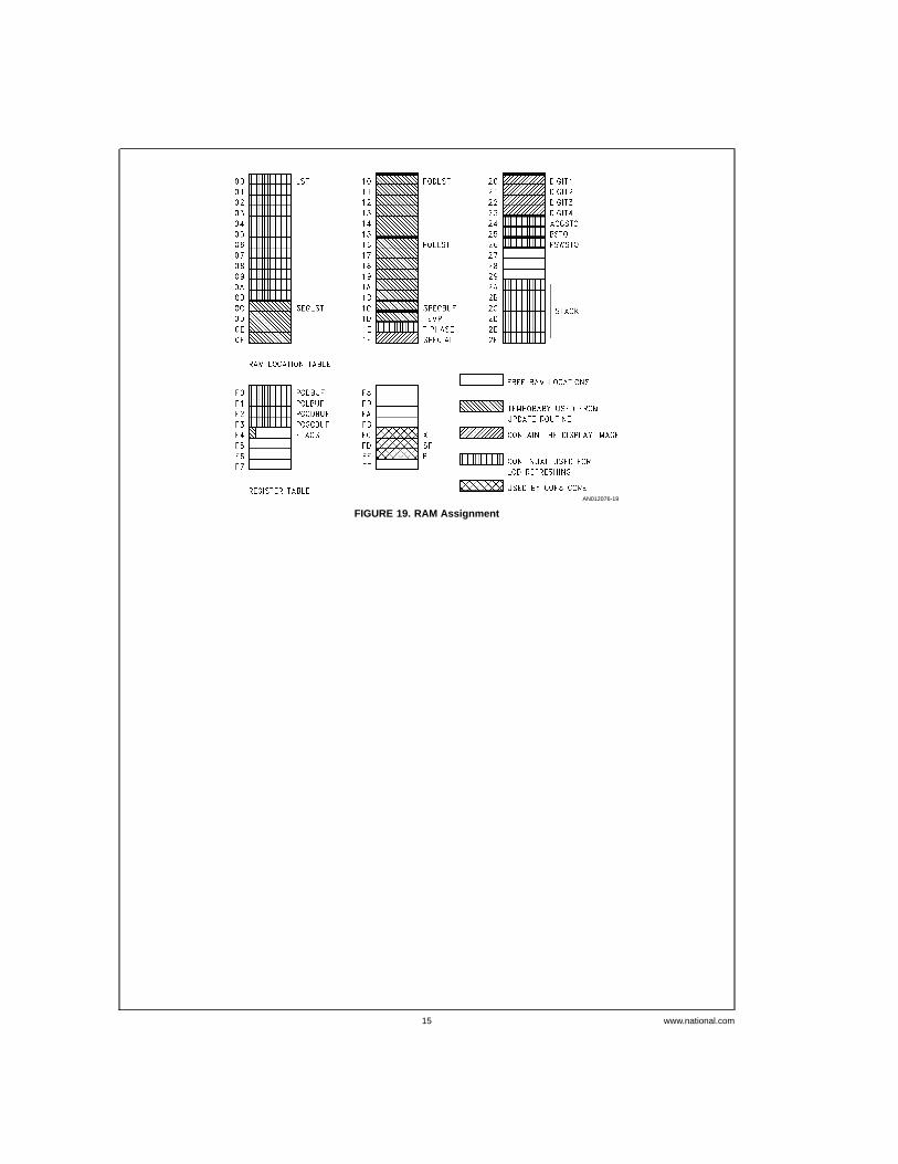
MEMORY REQUIREMENTS
ROM: 152 bytes incl. look up tables
RAM: 43 bytes (Figure 15 illustrates the RAM locations)
AN012076-14
FIGURE 14. Data Flow Chart for Update Routine
www.national.com9
AN012076-15
FIGURE 15. Data Flow Chart for Update Routine
www.national.com 10

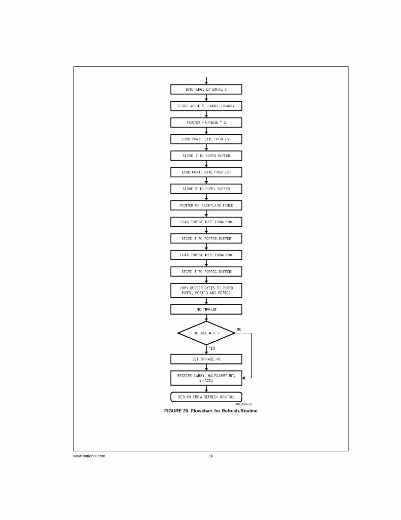
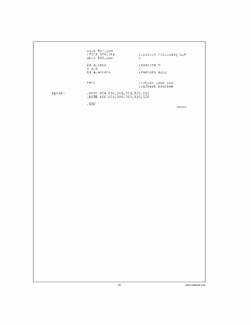
3. The refresh routine is the interrupt service routine of theexternal interrupt and is invoked at the beginning of a newtimephase. First the routine discharges the external capaci-tor and switches the G0/INT pin back to the input mode, toinitialize the next timephase. The backplane ports G2, G4and G5 and the segment pin ports D and L are updated bythis routine according to the actual timephase. For the back-planes the data are loaded from the bptab table in ROM.
Table 2 shows how the bptab values are gathered. Figure 20shows the flowchart for the refresh routine.
TIME REQUIREMENTS
The routine runs max. 150 cycles.
For a non flickering display, the refresh frequency must be30 Hz minimum. One refresh cycle has six timephases andis max. 33 ms long. So each timephase is 5.5 ms long. Withan oscillator (CKI) frequency of 2 MHz, one instruction cycletakes 1/(2 MHz/10) = 5 µs to execute. During one timephasethe controller can execute:
5.5 ms/5 µs = 1100 cycles. So the refresh routine needs 134/1100 = 0.122 = 12.2% of the whole processing time (in thiscase).
With a refresh frequency of 50 Hz the routine needs about20.1% of the whole processing time.
The refresh routine needs about 103 ROM bytes.
TABLE 2. Phase Values
Tiphase G5 G4 G2 Portg Data Hex Portg Config. Hex
0 0/0 0/0 1/1 XX00X1XX 04 XX00X1XX 04
1 0/0 1/1 0/0 XX01X0XX 10 XX01X0XX 10
2 1/1 0/0 0/0 XX10X0XX 20 XX10X0XX 20
3 0/0 0/0 0/1 XX00X0XX 00 XX00X1XX 04
4 0/0 0/1 0/0 XX00X0XX 00 XX01X0XX 10
5 0/1 0/0 0/0 XX00X0XX 00 XX10X0XX 20
data/configuration register of portg
0/0 : Hi-Z input
0/1 : output low
1/1 : output high
AN012076-16
FIGURE 16. Display Example
www.national.com11
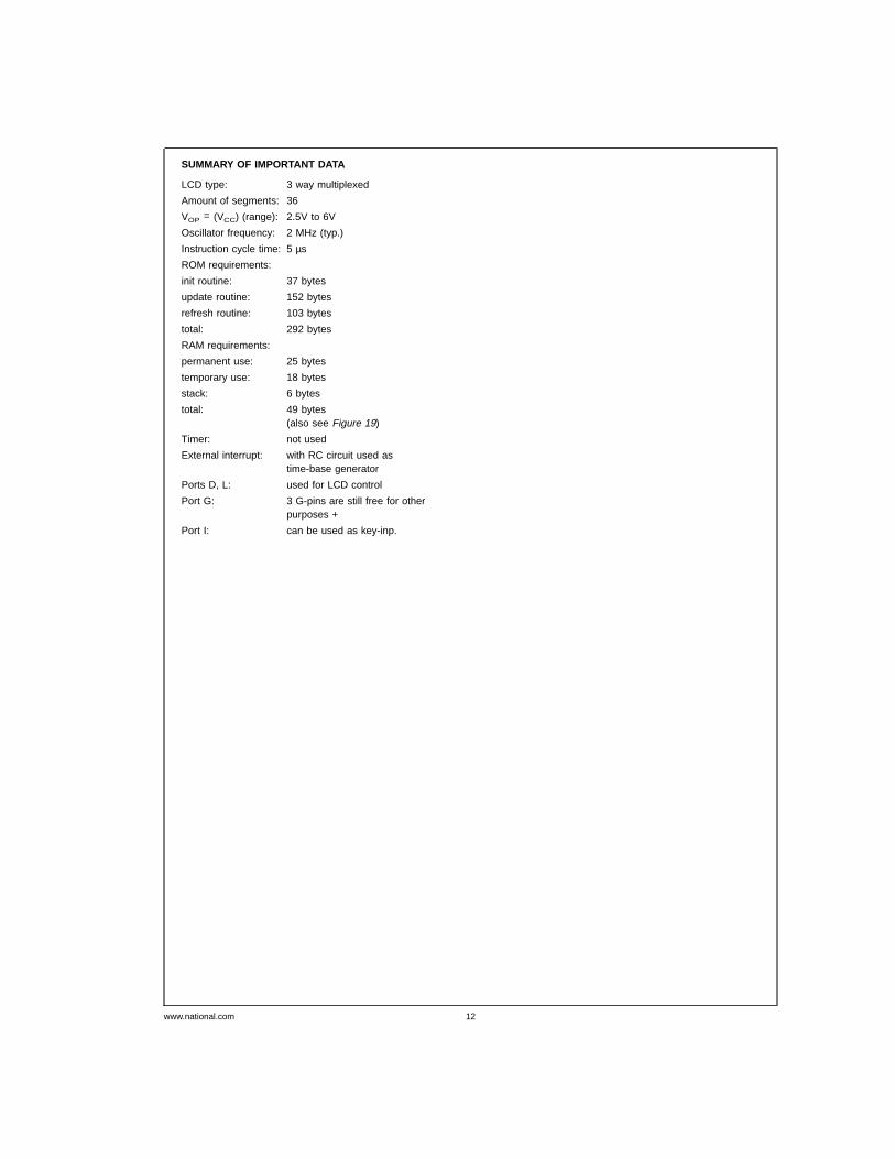
SUMMARY OF IMPORTANT DATA
LCD type: 3 way multiplexed
Amount of segments: 36
VOP = (VCC) (range): 2.5V to 6V
Oscillator frequency: 2 MHz (typ.)
Instruction cycle time: 5 µs
ROM requirements:
init routine: 37 bytes
update routine: 152 bytes
refresh routine: 103 bytes
total: 292 bytes
RAM requirements:
permanent use: 25 bytes
temporary use: 18 bytes
stack: 6 bytes
total: 49 bytes(also see Figure 19)
Timer: not used
External interrupt: with RC circuit used astime-base generator
Ports D, L: used for LCD control
Port G: 3 G-pins are still free for otherpurposes +
Port I: can be used as key-inp.
www.national.com 12
AN012076-17
FIGURE 17. Flowchart for Update Routine
www.national.com13
AN012076-18
FIGURE 18. Flowchart for Convert Subroutine
www.national.com 14
AN012076-19
FIGURE 19. RAM Assignment
www.national.com15
AN012076-20
FIGURE 20. Flowchart for Refresh-Routine
www.national.com 16
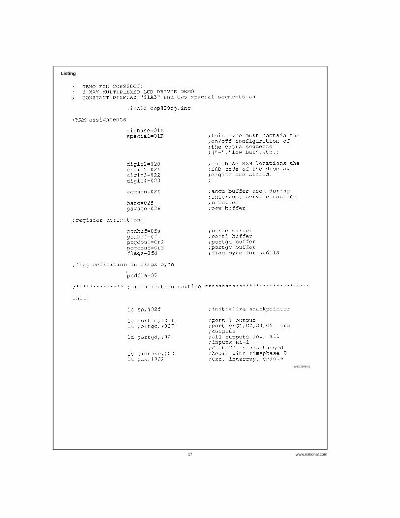
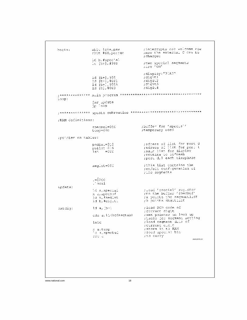
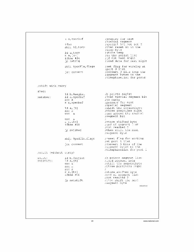
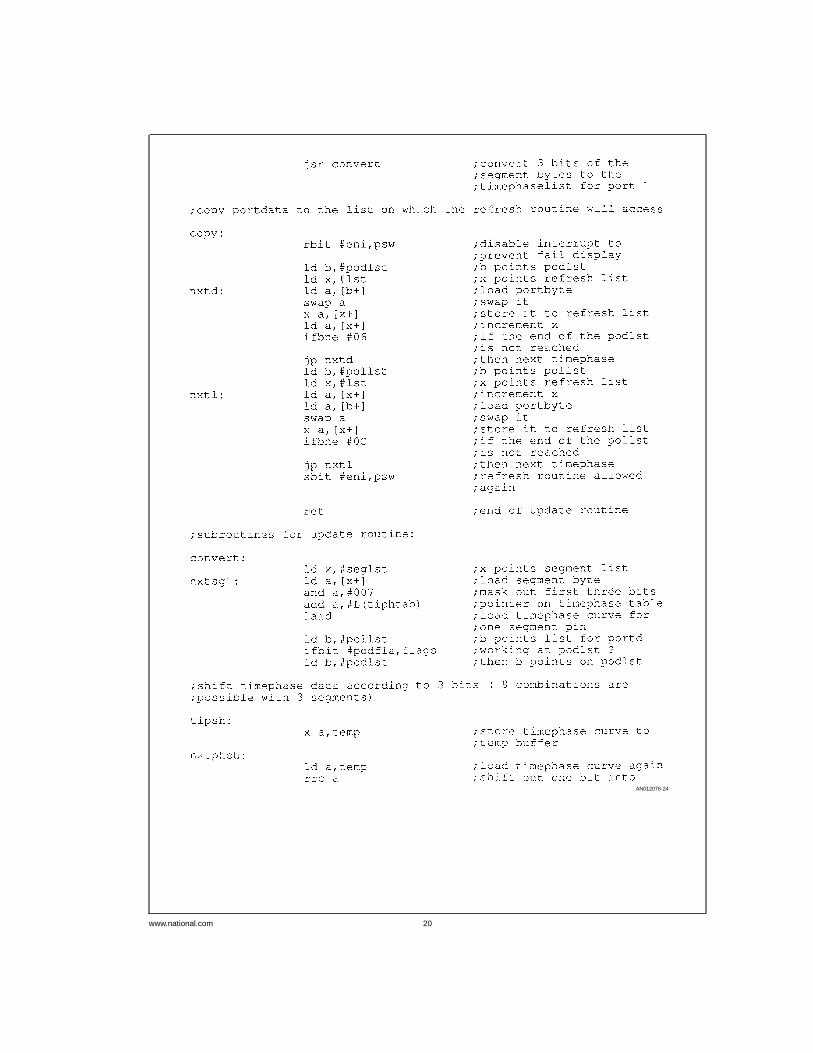
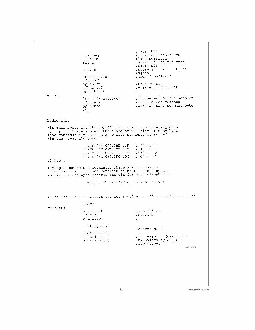
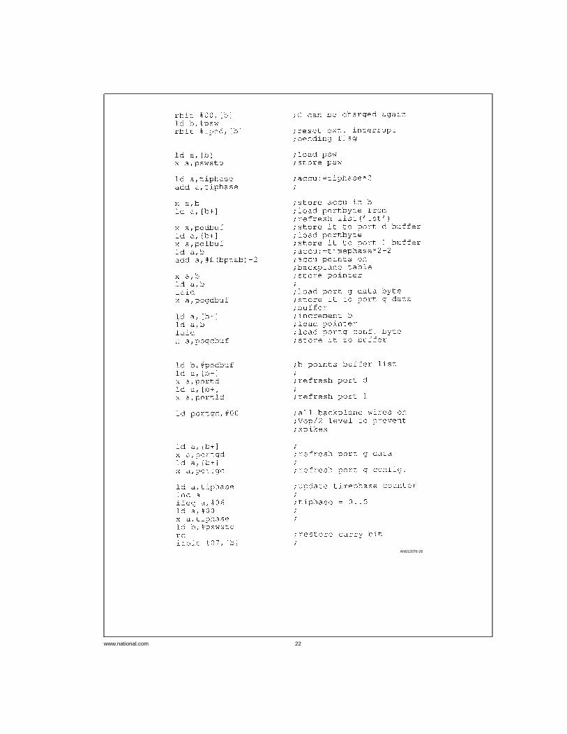
Listing
AN012076-21
www.national.com17
AN012076-22
www.national.com 18
AN012076-23
www.national.com19
AN012076-24
www.national.com 20
AN012076-25
www.national.com21
AN012076-26
www.national.com 22
AN012076-27
www.national.com23
LIFE SUPPORT POLICY
NATIONAL’S PRODUCTS ARE NOT AUTHORIZED FOR USE AS CRITICAL COMPONENTS IN LIFE SUPPORT DE-VICES OR SYSTEMS WITHOUT THE EXPRESS WRITTEN APPROVAL OF THE PRESIDENT OF NATIONAL SEMI-CONDUCTOR CORPORATION. As used herein:1. Life support devices or systems are devices or sys-
tems which, (a) are intended for surgical implant intothe body, or (b) support or sustain life, and whose fail-ure to perform when properly used in accordancewith instructions for use provided in the labeling, canbe reasonably expected to result in a significant injuryto the user.
2. A critical component is any component of a life supportdevice or system whose failure to perform can be rea-sonably expected to cause the failure of the life supportdevice or system, or to affect its safety or effectiveness.
National SemiconductorCorporationAmericasTel: 1-800-272-9959Fax: 1-800-737-7018Email: [email protected]
www.national.com
National SemiconductorEurope
Fax: +49 (0) 1 80-530 85 86Email: [email protected]
Deutsch Tel: +49 (0) 1 80-530 85 85English Tel: +49 (0) 1 80-532 78 32Français Tel: +49 (0) 1 80-532 93 58Italiano Tel: +49 (0) 1 80-534 16 80
National SemiconductorAsia Pacific CustomerResponse GroupTel: 65-2544466Fax: 65-2504466Email: [email protected]
National SemiconductorJapan Ltd.Tel: 81-3-5639-7560Fax: 81-3-5639-7507
AN
-953
LCD
Trip
lex
Driv
ew
ithC
OP
820C
J
National does not assume any responsibility for use of any circuitry described, no circuit patent licenses are implied and National reserves the right at any time without notice to change said circuitry and specifications.
IMPORTANT NOTICE
Texas Instruments Incorporated and its subsidiaries (TI) reserve the right to make corrections, modifications, enhancements, improvements,and other changes to its products and services at any time and to discontinue any product or service without notice. Customers shouldobtain the latest relevant information before placing orders and should verify that such information is current and complete. All products aresold subject to TI’s terms and conditions of sale supplied at the time of order acknowledgment.
TI warrants performance of its hardware products to the specifications applicable at the time of sale in accordance with TI’s standardwarranty. Testing and other quality control techniques are used to the extent TI deems necessary to support this warranty. Except wheremandated by government requirements, testing of all parameters of each product is not necessarily performed.
TI assumes no liability for applications assistance or customer product design. Customers are responsible for their products andapplications using TI components. To minimize the risks associated with customer products and applications, customers should provideadequate design and operating safeguards.
TI does not warrant or represent that any license, either express or implied, is granted under any TI patent right, copyright, mask work right,or other TI intellectual property right relating to any combination, machine, or process in which TI products or services are used. Informationpublished by TI regarding third-party products or services does not constitute a license from TI to use such products or services or awarranty or endorsement thereof. Use of such information may require a license from a third party under the patents or other intellectualproperty of the third party, or a license from TI under the patents or other intellectual property of TI.
Reproduction of TI information in TI data books or data sheets is permissible only if reproduction is without alteration and is accompaniedby all associated warranties, conditions, limitations, and notices. Reproduction of this information with alteration is an unfair and deceptivebusiness practice. TI is not responsible or liable for such altered documentation. Information of third parties may be subject to additionalrestrictions.
Resale of TI products or services with statements different from or beyond the parameters stated by TI for that product or service voids allexpress and any implied warranties for the associated TI product or service and is an unfair and deceptive business practice. TI is notresponsible or liable for any such statements.
TI products are not authorized for use in safety-critical applications (such as life support) where a failure of the TI product would reasonablybe expected to cause severe personal injury or death, unless officers of the parties have executed an agreement specifically governingsuch use. Buyers represent that they have all necessary expertise in the safety and regulatory ramifications of their applications, andacknowledge and agree that they are solely responsible for all legal, regulatory and safety-related requirements concerning their productsand any use of TI products in such safety-critical applications, notwithstanding any applications-related information or support that may beprovided by TI. Further, Buyers must fully indemnify TI and its representatives against any damages arising out of the use of TI products insuch safety-critical applications.
TI products are neither designed nor intended for use in military/aerospace applications or environments unless the TI products arespecifically designated by TI as military-grade or "enhanced plastic." Only products designated by TI as military-grade meet militaryspecifications. Buyers acknowledge and agree that any such use of TI products which TI has not designated as military-grade is solely atthe Buyer's risk, and that they are solely responsible for compliance with all legal and regulatory requirements in connection with such use.
TI products are neither designed nor intended for use in automotive applications or environments unless the specific TI products aredesignated by TI as compliant with ISO/TS 16949 requirements. Buyers acknowledge and agree that, if they use any non-designatedproducts in automotive applications, TI will not be responsible for any failure to meet such requirements.
Following are URLs where you can obtain information on other Texas Instruments products and application solutions:
Products Applications
Audio www.ti.com/audio Communications and Telecom www.ti.com/communications
Amplifiers amplifier.ti.com Computers and Peripherals www.ti.com/computers
Data Converters dataconverter.ti.com Consumer Electronics www.ti.com/consumer-apps
DLP® Products www.dlp.com Energy and Lighting www.ti.com/energy
DSP dsp.ti.com Industrial www.ti.com/industrial
Clocks and Timers www.ti.com/clocks Medical www.ti.com/medical
Interface interface.ti.com Security www.ti.com/security
Logic logic.ti.com Space, Avionics and Defense www.ti.com/space-avionics-defense
Power Mgmt power.ti.com Transportation and Automotive www.ti.com/automotive
Microcontrollers microcontroller.ti.com Video and Imaging www.ti.com/video
RFID www.ti-rfid.com
OMAP Mobile Processors www.ti.com/omap
Wireless Connectivity www.ti.com/wirelessconnectivity
TI E2E Community Home Page e2e.ti.com
Mailing Address: Texas Instruments, Post Office Box 655303, Dallas, Texas 75265Copyright © 2011, Texas Instruments Incorporated
Top Related