


Languages
Pages
Legal


MODULATION AND CONSTRAINED CODING TECHNIQUES FORWIRELESS INFRARED COMMUNICATION CHANNELS
by
Steve Hranilovic
A thesis submitted in conformity with the requirementsfor the degree of Master of Applied Science
Graduate Department of Electrical & Computer EngineeringUniversity of Toronto
c© Copyright by Steve Hranilovic 1999
Abstract
MODULATION AND CONSTRAINED CODING TECHNIQUES FOR
WIRELESS INFRARED COMMUNICATION CHANNELS
Steve Hranilovic
Master of Applied Science
Graduate Department of Electrical & Computer Engineering
University of Toronto
1999
Short-distance, point-to-point wireless infrared optical links provide a cost-effective
means of high speed data transfer between portable devices. To investigate such links, a test-
bench and circuits were constructed to determine the limitations of existing optoelectronics.
The results of these measurements are used to formulate a signal-space channel model
which is employed for the subsequent analysis of candidate bandwidth efficient modulation
schemes.
The modulation scheme Adaptively Biased QAM (AB-QAM) is developed based
on the channel model. AB-QAM provides an asymptotic 3 dB optical SNR improvement
over PAM while maintaining the same bandwidth efficiency. The use of constellation shaping
is shown to further improve the average optical power efficiency of AB-QAM.
This thesis proposes the use of constrained coding techniques to satisfy the non-
negativity constraint of the optical channel. These coding techniques are illustrated through
an example and contrasted to a baseline case. Constrained coding techniques allow greater
flexibility in the choice of pulse shapes used in the channel, leading to possible optical power
and bandwidth gains.
ii

Acknowledgements
This thesis has required a great deal of sacrifice and effort to complete. However, as
with any significant endeavour it was not accomplished without the help of a great number
of individuals.
I would like to express my sincere thanks to my supervisors, Professors David Johns
and Frank Kschischang. I appreciate the freedom they provided me to explore directions in
this thesis that were not originally anticipated. Also their patience and insightful comments
were key elements in the formulation of this work.
My parents have been a source of support not only during the writing of this
thesis but throughout my life. Although not involved in the technical aspects of this work,
their encouragement and perspective were integral to its completion. It is impossible to
adequately thank them for the love and care they have given me and continue to provide.
This work also reflects numerous conversations and debates with my colleagues in
room EA104. I thank them for the interest they took in my work as well as for their helpful
criticisms. However, foremost I would like to thank them for the friendship and camaraderie
they have displayed through my time at UofT.
Finally, I would like to acknowledge the financial support provided by the Natural
Sciences and Engineering Research Council of Canada through a post graduate scholarship.
iii

Table of Contents
List of Tables vi
List of Figures vii
1 Introduction and Motivation 11.1 Context . . . . . . . . . . . . . . . . . . . . . . . . . . . . . . . . . . . . . . 11.2 Survey of Current Implementations . . . . . . . . . . . . . . . . . . . . . . . 21.3 Research Direction . . . . . . . . . . . . . . . . . . . . . . . . . . . . . . . . 41.4 Thesis Structure . . . . . . . . . . . . . . . . . . . . . . . . . . . . . . . . . 5
2 Channel Modelling and Characterisation 62.1 The Wireless Optical Channel . . . . . . . . . . . . . . . . . . . . . . . . . . 6
2.1.1 Basic Channel Structure . . . . . . . . . . . . . . . . . . . . . . . . . 72.1.2 Eye Safety . . . . . . . . . . . . . . . . . . . . . . . . . . . . . . . . . 82.1.3 Channel Propagation Properties . . . . . . . . . . . . . . . . . . . . 10
2.2 Optoelectronic Components . . . . . . . . . . . . . . . . . . . . . . . . . . . 112.2.1 Light Emitting Devices . . . . . . . . . . . . . . . . . . . . . . . . . 112.2.2 Photodetectors . . . . . . . . . . . . . . . . . . . . . . . . . . . . . . 18
2.3 Experimental Channel . . . . . . . . . . . . . . . . . . . . . . . . . . . . . . 232.3.1 Circuit Design . . . . . . . . . . . . . . . . . . . . . . . . . . . . . . 232.3.2 Channel Measurements . . . . . . . . . . . . . . . . . . . . . . . . . 28
2.4 Noise . . . . . . . . . . . . . . . . . . . . . . . . . . . . . . . . . . . . . . . . 312.5 Summary of Characteristics and Conclusions . . . . . . . . . . . . . . . . . 34
3 Modulation Schemes 363.1 Definitions . . . . . . . . . . . . . . . . . . . . . . . . . . . . . . . . . . . . . 36
3.1.1 Channel Characteristics . . . . . . . . . . . . . . . . . . . . . . . . . 373.1.2 System Model . . . . . . . . . . . . . . . . . . . . . . . . . . . . . . . 383.1.3 Relating Channel Constraints to the Signal Space . . . . . . . . . . 403.1.4 Definition of Measures . . . . . . . . . . . . . . . . . . . . . . . . . . 43
3.2 Binary Level Modulation Schemes . . . . . . . . . . . . . . . . . . . . . . . 483.2.1 On-Off Keying . . . . . . . . . . . . . . . . . . . . . . . . . . . . . . 483.2.2 Pulse Position Modulation . . . . . . . . . . . . . . . . . . . . . . . . 503.2.3 Comparisons and Conclusions . . . . . . . . . . . . . . . . . . . . . . 54
iv

3.3 Multilevel Modulation Schemes . . . . . . . . . . . . . . . . . . . . . . . . . 553.3.1 Pulse Amplitude Modulation . . . . . . . . . . . . . . . . . . . . . . 553.3.2 Quadrature Pulse Amplitude Modulation . . . . . . . . . . . . . . . 573.3.3 Comparisons and Conclusions . . . . . . . . . . . . . . . . . . . . . . 60
3.4 Adaptively Biased QAM . . . . . . . . . . . . . . . . . . . . . . . . . . . . . 623.4.1 Modulation Scheme Definition . . . . . . . . . . . . . . . . . . . . . 633.4.2 Development . . . . . . . . . . . . . . . . . . . . . . . . . . . . . . . 643.4.3 Probability of Error Analysis . . . . . . . . . . . . . . . . . . . . . . 693.4.4 Coding and Shaping Gain in the AB-QAM Framework . . . . . . . . 743.4.5 Spectral Characteristics . . . . . . . . . . . . . . . . . . . . . . . . . 773.4.6 Extension of AB-QAM to Different Pulse Shapes . . . . . . . . . . . 803.4.7 Comparison with other Multilevel Schemes . . . . . . . . . . . . . . 81
3.5 Conclusions and Comparison . . . . . . . . . . . . . . . . . . . . . . . . . . 83
4 Constrained Coding Techniques for Intensity Modulated Channels 864.1 Motivation . . . . . . . . . . . . . . . . . . . . . . . . . . . . . . . . . . . . 864.2 Constrained Coding and Symbolic Dynamics . . . . . . . . . . . . . . . . . 884.3 A Constrained Code for Intensity Modulated Channels . . . . . . . . . . . . 92
4.3.1 Introduction . . . . . . . . . . . . . . . . . . . . . . . . . . . . . . . 924.3.2 Structure and Methods . . . . . . . . . . . . . . . . . . . . . . . . . 934.3.3 Results . . . . . . . . . . . . . . . . . . . . . . . . . . . . . . . . . . 964.3.4 Comparison to Baseline . . . . . . . . . . . . . . . . . . . . . . . . . 994.3.5 Code Construction . . . . . . . . . . . . . . . . . . . . . . . . . . . . 1024.3.6 Decoder Structure . . . . . . . . . . . . . . . . . . . . . . . . . . . . 103
4.4 Conclusions . . . . . . . . . . . . . . . . . . . . . . . . . . . . . . . . . . . . 108
5 Conclusions and Future Directions 1095.1 Conclusions . . . . . . . . . . . . . . . . . . . . . . . . . . . . . . . . . . . . 1095.2 Future Directions . . . . . . . . . . . . . . . . . . . . . . . . . . . . . . . . . 110
A Optimum Binary Pulse Set for Average Constrained Channels 112A.1 Introduction . . . . . . . . . . . . . . . . . . . . . . . . . . . . . . . . . . . . 112A.2 Problem Definition . . . . . . . . . . . . . . . . . . . . . . . . . . . . . . . . 112A.3 Development . . . . . . . . . . . . . . . . . . . . . . . . . . . . . . . . . . . 114
B Minimum Bandwidth, Non-Negative Nyquist Pulse 118B.1 Purpose . . . . . . . . . . . . . . . . . . . . . . . . . . . . . . . . . . . . . . 118B.2 Problem Definition . . . . . . . . . . . . . . . . . . . . . . . . . . . . . . . . 118B.3 Development . . . . . . . . . . . . . . . . . . . . . . . . . . . . . . . . . . . 119
Bibliography 123
v

List of Tables
1.1 Some key points of the IrDA 4 Mbps wireless infrared link specification [1]. 3
2.1 Interpretation of IEC safety classification for optical sources [2]. . . . . . . . 92.2 Point source safety classification based on allowable average optical power
output for a variety of optical wavelengths [3, 2]. . . . . . . . . . . . . . . . 102.3 Comparison of LEDs versus LDs for wireless optical links (based on [4, 5]) . 182.4 Comparison of p-i-n photodiodes versus avalanche photodiodes for wireless
optical links (based on [5, 6]) . . . . . . . . . . . . . . . . . . . . . . . . . . 232.5 Measurement results of experimental free-space optical link. . . . . . . . . . 31
4.1 Sliding block decoder for 4b-3s code considered in the example. u is thecurrent input block and v is the previous input block. r is the decoded blockof binary data represented in decimal format. The entries denoted by “∗”indicate that any block may be received in this interval. . . . . . . . . . . . 107
vi

List of Figures
2.1 Basic channel structure of a wireless optical link. . . . . . . . . . . . . . . . 72.2 An example of a one dimensional variation of band edges with wave number
(k) for (a) direct band gap material, (b) indirect band gap material [7]. . . 122.3 An example of an AlGaAs/GaAs/AlGaAs double heterostructure LED (a)
construction and (b) band diagram under forward bias [8, 9]. . . . . . . . . 142.4 An example of an optical intensity versus drive current for LED and LD [10] 162.5 Relative sensitivity curve for a silicon photodiode [11]. Note that the posi-
tion of the GaAs emission line is located near the peak in sensitivity of thephotodiode. . . . . . . . . . . . . . . . . . . . . . . . . . . . . . . . . . . . . 19
2.6 Structure of a simple silicon p-i-n photodiode [12]. . . . . . . . . . . . . . . 202.7 Schematic of transmit transconductance amplifier and test setup. . . . . . . 242.8 Measurement results of transmit transconductor : (a) frequency response and
(b) harmonic distortion. . . . . . . . . . . . . . . . . . . . . . . . . . . . . . 252.9 Schematic of receive transimpedance amplifier and test setup. . . . . . . . . 272.10 Measurement results of receive transimpedance amplifier : (a) frequency re-
sponse and (b) harmonic distortion. . . . . . . . . . . . . . . . . . . . . . . 282.11 Photographs of the transmit and receive electronics with test optoelectronics
mounted in test fixture. . . . . . . . . . . . . . . . . . . . . . . . . . . . . . 292.12 Frequency response (a) and harmonic distortion (20 MHz input tone) (b)
measurements of link. . . . . . . . . . . . . . . . . . . . . . . . . . . . . . . 30
3.1 A conceptualised communication model of the wireless optical link for anisolated pulse si(t) (following [13]). . . . . . . . . . . . . . . . . . . . . . . . 38
3.2 Basis function (a) and constellation (b) of on-off keying. . . . . . . . . . . . 493.3 The continuous portion of the power spectral density of on-off keying, for
RP = 1 and Ts = 1. . . . . . . . . . . . . . . . . . . . . . . . . . . . . . . . 503.4 Basis functions for 4-PPM. . . . . . . . . . . . . . . . . . . . . . . . . . . . 513.5 The continuous portion of the power spectral density of 4-PPM, for RP = 1
and Ts = 1. . . . . . . . . . . . . . . . . . . . . . . . . . . . . . . . . . . . . 543.6 Basis function (a) and constellation (b) of pulse amplitude modulation (where
∆ = 2RPL−1
√Ts). . . . . . . . . . . . . . . . . . . . . . . . . . . . . . . . . . . 56
3.7 The continuous portion of the power spectral density of 5-PAM, for RP = 1and Ts = 1. . . . . . . . . . . . . . . . . . . . . . . . . . . . . . . . . . . . . 58
vii
3.8 Basis function (a) and L2 = 16 point constellation (b) of quadrature pulseamplitude modulation (for ωp = 2π/Ts). . . . . . . . . . . . . . . . . . . . . 59
3.9 The continuous portion of the power spectral density of 25-QAM, for RP = 1and Ts = 1. . . . . . . . . . . . . . . . . . . . . . . . . . . . . . . . . . . . . 61
3.10 Basis functions for AB-QAM. . . . . . . . . . . . . . . . . . . . . . . . . . . 643.11 Distribution of symbol averages for 5-PAM and 5-AB-PAM (dmin = 1, R = 1
and Ts=1). . . . . . . . . . . . . . . . . . . . . . . . . . . . . . . . . . . . . 663.12 Constellations for 5-PAM and 5-AB-PAM for P = 1, R = 1 and Ts=1. . . . 673.13 Constellations of 5-AB-PAM and 6-AB-PAM in the φ2 and φ3 dimensions.
Note the bold lines indicate the dmin of the constellation, and ∆ indicatesthe one-dimensional minimum distance. . . . . . . . . . . . . . . . . . . . . 68
3.14 Two views of the constellations for 16-AB-QAM and 25-AB-QAM for ∆ = 1,R = 1 and Ts=1 in each. Bold lines indicate minimum distance betweenconstellation points, while the dotted lines connect points of equal symbolaverage. . . . . . . . . . . . . . . . . . . . . . . . . . . . . . . . . . . . . . . 72
3.15 Comparison of simulated symbol error rates to approximations in (3.35) and(3.37), with Ts=1 s, P=1 W, R=0.9 and σ2
n = 10−2 W/Hz. . . . . . . . . . 733.16 Shaped constellation for 25-AB-QAM for ∆ = 1, R = 1 and Ts=1 in each. . 763.17 Shaped constellation for 64-AB-QAM for ∆ = 1, R = 1 and Ts=1 in each. . 783.18 The continuous portion of the power spectral density of 25-AB-QAM, for
RP = 1 and Ts = 1. . . . . . . . . . . . . . . . . . . . . . . . . . . . . . . . 793.19 Comparison of bit error rates versus optical signal-to-noise ratio for 49-
QAM, 7-PAM, 49-AB-QAM and shaped 49-AB-QAM (R = 1 A/W, σ2n =
10−2 W/Hz, B = 2 Hz and Rb = log2(49) bits/s). . . . . . . . . . . . . . . . 823.20 Comparison of bit error rates versus optical signal-to-noise ratio for 64-
QAM, 8-PAM, 64-AB-QAM and shaped 64-AB-QAM (R = 1 A/W, σ2n =
10−2 W/Hz, B = 2 Hz and Rb = 6 bits/s). . . . . . . . . . . . . . . . . . . . 823.21 Comparison of power efficiency gain of modulation schemes over OOK plotted
versus bandwidth efficiency. . . . . . . . . . . . . . . . . . . . . . . . . . . . 84
4.1 Graph G representing the (1,2) run-length limited shift. . . . . . . . . . . . 914.2 The family of pulse shapes used for the example PAM scheme. . . . . . . . 944.3 Description of the coder and the pulse shape used in the example, where D
indicates a delay of one interval. . . . . . . . . . . . . . . . . . . . . . . . . 944.4 Topological entropy, h(X) in bits/symbol, of each modulation scheme over
k1 and L. . . . . . . . . . . . . . . . . . . . . . . . . . . . . . . . . . . . . . 974.5 Average output amplitude of each modulation scheme over k1 and L. . . . . 984.6 Same data as figure 4.5, where dashed lines connect points of equal entropy
h(X) bits/symbol. . . . . . . . . . . . . . . . . . . . . . . . . . . . . . . . . 994.7 Description of the baseline scheme. . . . . . . . . . . . . . . . . . . . . . . . 1004.8 Power gain G (dB) of constrained coding technique over baseline case versus
topological entropy, h(X) in bits/symbol. . . . . . . . . . . . . . . . . . . . 1014.9 State transition diagram of the example 4b-3s coder (Note: edges are labelled
with the pairs input/output). . . . . . . . . . . . . . . . . . . . . . . . . . . 104
viii

4.10 Critical signals in the 4b-3s code example : (a) the input sequence (in decimalformat), (b) the output of the coder, (c) the output intensity signal of thefilter. . . . . . . . . . . . . . . . . . . . . . . . . . . . . . . . . . . . . . . . . 105
A.1 Graphical representation of re-arranged problem definition in (A.4) in theplane containing γ1 and γ2. . . . . . . . . . . . . . . . . . . . . . . . . . . . 115
B.1 Time Domain Representation of (2) and observation on first derivative of p(t) 120B.2 Real and Imaginary Components of P (ω) . . . . . . . . . . . . . . . . . . . 121
ix

Chapter 1
Introduction and Motivation
1.1 Context
In recent years, there has been a migration of computing power from the desktop
to portable, mobile formats. Devices such as digital still and video cameras, portable digital
assistants and laptop computers offer users the ability to process and capture vast quan-
tities of data. Although convenient, the interchange of data between such devices remains
a challenge due to their small size, portability and low cost. A high performance link is
necessary to allow data exchange from these portable devices to established computing in-
frastructure such as backbone networks, data storage devices and user interface peripherals.
Also, the ability to form ad hoc networks between portable devices remains an attractive
application. The links considered need to operate over relatively short distances, on the
order of centimetres. These types of links would be useful for the interchange of data when
the two communicating devices were in close proximity to one another. This type of link
can be seen as a means of transferring data between portable devices or between a portable
device and a fixed computer. Several solutions have been proposed to fulfil this need for a
short distance high speed link.
The use of a direct electrical connection between portable devices and a host is
a simple means of establishing a link. This electrical connection is made via a cable and
connectors on both ends or by some other direct connection method. The connectors can
be expensive due to the small size of the portable device. In addition, these connectors
are prone to wear and break with repeated use. The physical pin-out of the link is fixed
and incompatibility among various vendors solutions may exist. Also, the need to carry the
1

Section 1.2. Survey of Current Implementations 2
physical medium for communication makes this solution inconvenient for the user.
Wireless radio frequency (RF) solutions alleviate most of the disadvantages of a
fixed electrical connection. RF wireless solutions allow a short distance link to be established
without any physical connection. However, these solutions remain relatively expensive and
have low data rates. A recently proposed “low cost” RF link over short distances provides
data rates of 730 kbps in the 2.4 GHz band for a cost of US$10 per module [14]. Another
factor which increases the cost of RF wireless links are the spectrum licensing fees paid to
federal regulatory bodies. These frequency allocations are determined by local authorities
and may vary from country to country, making a standard interface difficult. In addition,
the broadcast nature of the RF channel creates problems with interference between devices
communicating to a host in close proximity. Containment of electromagnetic energy at RF
frequencies is difficult and if improperly done can impede system performance.
Wireless optical links provide a high data rate, low cost option to fulfil this short
distance communication application. Present day wireless optical links can transmit at
4 Mbps over short distances using optoelectronic devices which cost approximately US$1
[15]. Since the electromagnetic spectrum is not licensed in the infrared range, spectrum
licensing fees are avoided, further reducing system cost. Optical radiation in the infrared
or visible range is easily contained by opaque boundaries. As a result, interference between
adjacent devices can be minimised easily and economically. In contrast to direct electrical
connections, a wireless infrared link can be programmed to support many different protocols
which can be managed automatically by the device. Wireless optical links are also suited to
portable devices since small surface mount light emitting and light detecting components
are available in high volumes at relatively low cost.
1.2 Survey of Current Implementations
The Infrared Data Association (IrDA) is a group of industrial partners which
specify hardware and software specifications for short distance infrared links [15]. Currently,
the most popular link is a 4 Mbps serial point-to-point link which operates over a distance
of a metre with optical emissions conforming to stringent class 1 eye safety levels [1]. Table
1.1 summarises some key points of the IrDA short distance wireless specification 1. The1The classification of optical radiating devices in terms of their eye safety limits is discussed in Section
2.1.2. Chapter 3 defines PPM and presents an analysis of error performance.

Section 1.2. Survey of Current Implementations 3
Link Type Line-of-sightModulation Scheme 4-PPMBit Rate 4 MbpsBit Error Rate 10−8
Range Min : 0 m ; Max : 1 m
Table 1.1: Some key points of the IrDA 4 Mbps wireless infrared link specification [1].
restrictions of this specification are commonly satisfied with inexpensive optoelectronics
and without the need of extensive signal processing at the receiver. Over 60 million devices
satisfying the IrDA specification have already been installed in laptop computers, digital
cameras, printers, cellular phones and other portable computing equipment. It is projected
that the short distance infrared market is growing at 40% per annum and will reach world
wide sales of US$290 million dollars by 2002 [15, 16].
The IrDA has also recently extended its specification to 16 Mbps links over short
distances. The standard was finalised in March 1999, and products are expected to ship by
year end. Work has already started on extending this new standard to 32 Mbps in the near
future [17].
A simple extension of point-to-point links are telepoint links in which a wider
diverging beam is used to establish a one to many connection. A network base station
may be mounted on the ceiling and provide access to a limited number of terminals. Each
terminal, however, requires a line-of-sight link to the base station. The IrDA has started
work on an advanced infrared (AIR) specification for just such a link. Prototype links
are expected by year end which would provide 4 Mbps operation in a radius of 4 m, and
250 kbps in a radius of 8 m [18]. Others have extended this system to provide a shared
10 Mbps wireless infrared extension to an Ethernet network over a range of 10 m from the
base station. Approximately six users can be accommodated per base station [19].
Another direction for wireless infrared links has been towards diffuse multipoint
links. These types of links require base station satellites which are mounted on the ceiling or
wall and communicate to many portable devices. These devices offer the freedom to move
about a room while maintaining the data link. A line of site path is not required for the
link to be established, since reflected paths are used as well. An example of a diffuse optical
link operates at rates as high as 4 Mbps over a coverage area of approximately 90 m2 [20].
The operation of this type of link is, however, highly dependent on the room layout and the
composition of the walls [3].
Section 1.3. Research Direction 4
Longer distance free-space optical links have been constructed to provide a high
data rate wireless link. They are used primarily for inter-building communications or to
provide a portable redundant link for fibre optic and video systems. These systems operate
exclusively outdoors due to the high optical power used. Long distance wireless infrared
links have been shown to allow up to 622 Mbps data rates for distances as long as one
kilometre [21]. Prototype links have also been constructed which provide a 1 Gbps data
rate over 40 m distances [22]. All long distance wireless optical systems are degraded by
atmospheric conditions, especially fog. The availability of these links has been shown to be
approximately 99.99% which is insufficient for some backbone telecommunication systems.
1.3 Research Direction
Short distance wireless optical links are an economical and convenient means to
transfer data to a portable device. The use of inexpensive optoelectronics in the 880 nm
band will allow these inexpensive links to be used in a wide variety of applications.
The goal of this research is to initiate work on the construction of a short range,
wireless optical link capable of data rates in the gigabit per second range. This link must be
constructed using inexpensive optoelectronic components, so as to encourage its application
over a wide variety of computing devices. The proposed range of communication is on the
order of centimetres. It is also required that the output of the link remain eye safe so that
the conditions of operation are not limited.
A potential application for this type of high speed, short distance link would be
for data transfer between a small, portable personal computing device and other computing
infrastructure. This type of link would allow a user to carry a note pad sized device which
would house all data processing and storage elements. The portable device would have some
rudimentary user interface, perhaps using handwriting recognition, to allow work to be done
while away from network connections. The short infrared link could be used to connect this
device to an interface unit when in a wired location. This interface unit would provide the
portable device with a network connection, a connection to user interface peripherals and
would display video images sent from the portable unit. In this manner, the interface unit
would become an inexpensive shell for use with any unit, and could be placed in public
locations. The infrared link would provide a robust means of linking the portable device to
the interface unit. This wireless optical link could also be used to link two portable devices
to transfer data when away from computing infrastructure. In this manner, the wireless

Section 1.4. Thesis Structure 5
optical link provides a universal port for all data entering or leaving the portable personal
computing device.
Another application for this type of link is in the digital video imaging arena. Vast
quantities of data can be collected in short times using digital video cameras. Transferring
these large amount of data directly into a network via a short distance infrared link would
be convenient and efficient. In order to move these large amounts of data in a reasonable
amount of time, a high data rate link is required. An inexpensive, short range, wireless
optical link would be well suited to this task.
In summary, the proposed high data rate infrared link over short distances would
provide a robust and inexpensive data port for a variety of next generation portable com-
puting devices.
1.4 Thesis Structure
The goal of this thesis is to investigate system issues involved in transmitting data
over wireless infrared links at high data rates. In order to begin to consider the system
issues of such a link, preliminary channel characteristics are required. Chapter 2 describes
the basic channel structure of wireless infrared channels. A more detailed description of
channel characteristics follows through the use of device physics and measurements from an
experimental channel.
Chapter 3 uses the characteristics and constraints of the wireless optical channel
to evaluate a variety of modulation schemes for the channel. Conventional binary level
modulation schemes are shown to provide insufficient bandwidth efficiency, while multi-
level schemes do not provide sufficient power efficiency. The modulation scheme adaptively
biased QAM is proposed and shown as a bandwidth efficient alternative with favourable
power efficiency. The use of constellation shaping is also investigated to improve the power
efficiency of the scheme.
Chapter 4 describes an alternate method of satisfying the non-negativity constraint
of the wireless optical channel. The use of constrained coding to satisfy channel constraints
allows the use of symbol pulses which individually do not satisfy the channel constraints.
This gives the system designer the freedom to choose pulses with favourable spectral or
average optical power characteristics.
The thesis concludes in chapter 5 with a summary of the results as well as some
directions for future work.

Chapter 2
Channel Modelling and
Characterisation
In order to proceed with the design of a high-speed wireless optical link, a basic
knowledge of the channel characteristics is required. This chapter presents a high-level
overview of the characteristics and constraints of wireless optical links. The basic chan-
nel characteristics are further illuminated by an overview of the device physics governing
optoelectronic devices. On the basis of device behaviour, a comparison between popular
devices is used to justify the design choices. The chapter continues with a description of the
experimental apparatus constructed to determine channel bandwidth and linearity. Experi-
mental results are presented on the performance of test circuitry as well as on the free-space
optical link. Various noise sources present in the free space optical link are also discussed
to determine which are dominant.
The chapter concludes with a summary of the main topics covered. The choice
of optoelectronic components is justified. Conclusions on the channel structure are drawn
based on measurements and noise considerations.
2.1 The Wireless Optical Channel
Wireless optical channels differ in several key ways from conventional communica-
tions channels treated extensively in literature. This section presents introductory remarks
on the channel characteristics and structure.
6

Section 2.1. The Wireless Optical Channel 7
ElectricalSignal
ReceiveElectronics
TransmitElectronics
ElectricalSignal
Light Emitter
x(t)
Optical IntensitySignal
Light Detector
itx(t) irx(t)
Figure 2.1: Basic channel structure of a wireless optical link.
2.1.1 Basic Channel Structure
In a wireless optical channel, information is transmitted by sending a time varying
optical signal between the transmitter and receiver. The information sent on this channel
is not contained in the amplitude, phase or frequency of the transmitted optical waveform,
but rather in the intensity of the transmitted signal. Present day optoelectronics cannot
operate directly on the frequency or phase of the 1014 Hz range optical signal. Instead, only
the intensity, defined as the power per area in W/m2, can be modulated or detected by the
optoelectronics.
On a conceptual level, the operation of optoelectronic devices can be seen as per-
forming a conversion between the optical domain, where the signal is a time varying inten-
sity, and the electrical domain, where the information is sent as a current signal. In ideal
devices, the conversion between the two signal domains is governed by a linear proportion-
ality constant. The operation of some popular optoelectronic components is described in
more detail in Sections 2.2.1 and 2.2.2.
The operation of a wireless optical channel is outlined in Figure 2.1. The transmit
electronics convert an input data stream into a time varying current, itx(t). This current is
used to drive a light emitting device to produce the output optical radiation. The electrical
characteristics of the light emitter can be modelled as a diode, as shown in the figure. The
electrical current signal is converted to an optical intensity signal, x(t), by the light emitter.
The intensity signal x(t) ideally is proportional to the magnitude of the electrical signal
current, itx(t).
This optical radiation propagates through free-space until it reaches the light de-
tector at the receive side of the link. The light detector is often termed a square law device
Section 2.1. The Wireless Optical Channel 8
since its operation is modelled as squaring the amplitude of the incoming electromagnetic
signal and integrating over time to find the intensity. The output of the light detector is
a current signal, irx(t), proportional to the intensity of the received optical signal. The
electrical operation of this device is most often modelled as a reverse biased diode, as shown
in Figure 2.1. This received electrical current signal is amplified and the digital information
detected.
The fact that the optical channel is an intensity modulated one, adds constraints on
the class of signals which may be transmitted. The information bearing intensity signal must
remain positive for all time since the transmitted power can physically never be negative.
Thus, the physics of the link imposes the fundamental constraint that the transmitted
signals remain non-negative for all time.
2.1.2 Eye Safety
Safety considerations must be taken into account when designing a wireless optical
link. Since the energy is propagated in a free-space channel, the impact of this radiation on
eye safety must be considered.
The International Electrotechnical Commission (IEC) is the standards body which
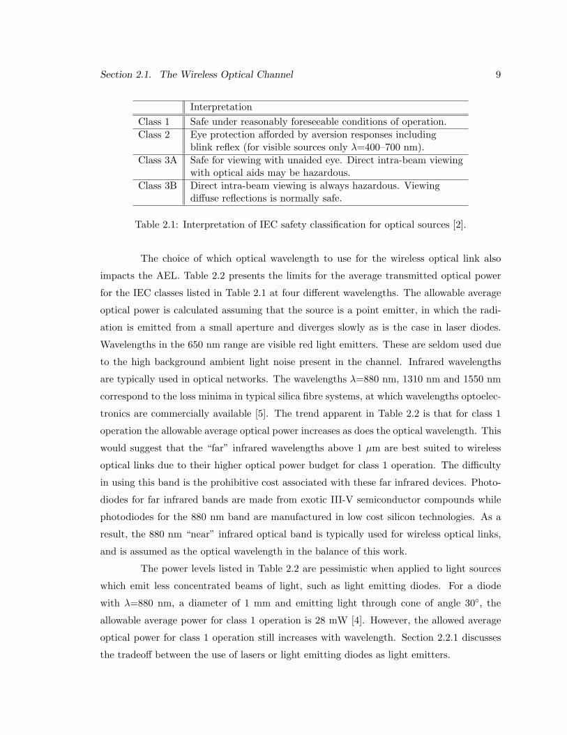
classifies exposure limits of optical sources. Table 2.1 includes a list of the primary classes
under which an optical radiator can fall. Class 1 operation is most desirable for a wireless
optical system since emissions from products are safe under all circumstances. Under these
conditions, no warning labels need to be applied and the device can be used without special
safety precautions. This is important since these optical links are destined to be inexpensive,
portable and convenient for the user. Longer distance free-space links often operate in class
3B mode, and are used for high data rate transmission over moderate distances (40 m in
[22]). The safety of these systems is maintained by locating optical beams on rooftops or
on towers to prevent inadvertent interruption [3].
The critical parameter which determines whether a source falls into a given class
depends on the application. The allowable exposure limit (AEL) depends on the wavelength
of the optical source, the geometry of the emitter and the intensity of the source. For high
frequency modulated sources, the average transmitted power of modulation scheme used
sets the AEL for a given geometry and wavelength. At modulation frequencies greater than
about 24 kHz, the AEL can be calculated based on average output power of the source [4].
Section 2.1. The Wireless Optical Channel 9
InterpretationClass 1 Safe under reasonably foreseeable conditions of operation.Class 2 Eye protection afforded by aversion responses including
blink reflex (for visible sources only λ=400–700 nm).Class 3A Safe for viewing with unaided eye. Direct intra-beam viewing
with optical aids may be hazardous.Class 3B Direct intra-beam viewing is always hazardous. Viewing
diffuse reflections is normally safe.
Table 2.1: Interpretation of IEC safety classification for optical sources [2].
The choice of which optical wavelength to use for the wireless optical link also
impacts the AEL. Table 2.2 presents the limits for the average transmitted optical power
for the IEC classes listed in Table 2.1 at four different wavelengths. The allowable average
optical power is calculated assuming that the source is a point emitter, in which the radi-
ation is emitted from a small aperture and diverges slowly as is the case in laser diodes.
Wavelengths in the 650 nm range are visible red light emitters. These are seldom used due
to the high background ambient light noise present in the channel. Infrared wavelengths
are typically used in optical networks. The wavelengths λ=880 nm, 1310 nm and 1550 nm
correspond to the loss minima in typical silica fibre systems, at which wavelengths optoelec-
tronics are commercially available [5]. The trend apparent in Table 2.2 is that for class 1
operation the allowable average optical power increases as does the optical wavelength. This
would suggest that the “far” infrared wavelengths above 1 µm are best suited to wireless
optical links due to their higher optical power budget for class 1 operation. The difficulty
in using this band is the prohibitive cost associated with these far infrared devices. Photo-
diodes for far infrared bands are made from exotic III-V semiconductor compounds while
photodiodes for the 880 nm band are manufactured in low cost silicon technologies. As a
result, the 880 nm “near” infrared optical band is typically used for wireless optical links,
and is assumed as the optical wavelength in the balance of this work.
The power levels listed in Table 2.2 are pessimistic when applied to light sources
which emit less concentrated beams of light, such as light emitting diodes. For a diode
with λ=880 nm, a diameter of 1 mm and emitting light through cone of angle 30, the
allowable average power for class 1 operation is 28 mW [4]. However, the allowed average
optical power for class 1 operation still increases with wavelength. Section 2.2.1 discusses
the tradeoff between the use of lasers or light emitting diodes as light emitters.

Section 2.1. The Wireless Optical Channel 10
650 nm 880 nm 1310 nm 1550 nmvisible infrared infrared infrared
Class 1 < 0.2 mW < 0.5 mW < 8.8 mW < 10 mWClass 2 0.2–1 mW n/a n/a n/aClass 3A 1–5 mW 0.5–2.5 mW 8.8–45 mW 10–50 mWClass 3B 5–500 mW 2.5–500 mW 45–500 mW 50–500 mW
Table 2.2: Point source safety classification based on allowable average optical power outputfor a variety of optical wavelengths [3, 2].
Eye safety considerations limit the average optical power which can be transmitted.
This is another fundamental limit on the performance of free-space optical links. Therefore,
the constraint on any modulation scheme constructed for wireless optical links is that the
average optical power is limited.
2.1.3 Channel Propagation Properties
As is the case in radio frequency transmission systems, multipath propagation
effects are important for wireless optical networks. The power launched from the transmitter
may take many reflected and refracted paths before arriving at the receiver. In radio
systems, the sum of the transmitted signal and its images at the receive antenna cause
spectral nulls in the transmission characteristic. These nulls are located at frequencies
where the phase shift between the paths causes destructive interference at the receiver.
This effect is known as multipath fading [13].
Unlike radio systems, multipath fading is not a major impairment in wireless
optical transmission. The “antenna” in a wireless optical system is the light detector which
typically has an active radiation collection area of approximately 1 cm2. The relative size
of this antenna with respect to the wavelength of the infrared light is immense, on the order
of 104λ. The multipath propagation of light produces fades in the amplitude of the received
electromagnetic signal at spacings on the order of half a wavelength apart. As mentioned
earlier, the light detector is a square law device which integrates the square of the amplitude
of the electromagnetic radiation impinging on it. The large size of the detector with respect
to the wavelength of the light provides a degree of inherent spatial diversity in the receiver
which mitigates the impact of multipath fading [23].
Although multipath fading is not a major impediment to wireless optical links,
temporal dispersion of the received signal due to multipath propagation remains a prob-
lem. This dispersion is often modelled as a linear time invariant system since the channel

Section 2.2. Optoelectronic Components 11
properties change slowly over many symbol periods. The impact of multipath dispersion is
most noticeable in diffuse infrared communication systems. In short distance line-of-sight
(LOS) links, multipath dispersion is seldom an issue. Indeed, channel models proposed for
LOS links assume the LOS path dominates and model the channel as a linear attenuation
and delay. Thus, for the short range optical links considered in this work, multipath effects
are not significant [24, 25, 26].
2.2 Optoelectronic Components
The basic channel characteristics can be investigated more fully by considering the
operation of the optoelectronic devices alone. Device physics provides significant insight into
the operation of these optoelectronic devices. This section presents an overview of the basic
device physics governing the operation of certain optoelectronic devices, emphasising their
benefits and disadvantages for wireless optical applications.
2.2.1 Light Emitting Devices
Solid state light emitting devices are essentially diodes operating in forward bias
which output an optical intensity approximately linearly related to the drive current. This
output optical intensity is due to the fact that a large proportion of the injected minority
carriers recombine giving up their energy as emitted photons.
To ensure a high probability of recombination events causing photon emission, light
emitting devices are constructed of materials known as direct band gap semiconductors. In
this type of crystal, the extrema of the conduction and valence bands coincide at the same
value of wave vector. As a result, recombination events can take place across the band gap
while conserving momentum, represented by the wave vector (as seen in Figure 2.2)[9]. A
majority of photons emitted by this process have energy Ephoton = Eg = hν, where Eg is
the band gap energy, h is Planck’s constant and ν is the photon frequency in hertz. This
equation can be re-written in terms of the wavelength of the emitted photon as
λ =1240Eg
(2.1)
where λ is the wavelength of the photon in nm and Eg is the band gap of the material in
electron-Volts. Commercial direct band gap materials are typically compound semiconduc-
tors of group III and group V elements. Examples of these types of crystals include: GaAs,
InP, InGaAsP and AlGaAs (for Al content less than ≈ 0.45) [8].

Section 2.2. Optoelectronic Components 12
(a) (b)
+k-k
Electron Energy
Eg
+k-k
Electron Energy
Egphoton
phonon
Conduction Band
photon
Valence Band
Conduction Band
Valence Band
hν
hν
Figure 2.2: An example of a one dimensional variation of band edges with wave number (k)for (a) direct band gap material, (b) indirect band gap material [7].
Elemental semiconducting crystals silicon and germanium are indirect band gap
materials. In these types of materials, the extrema of conduction and valence bands do not
coincide at the same value of wave vector k, as shown in Figure 2.2. Recombination events
cannot occur without a variation in the momentum of the interacting particles. The required
change in momentum is supplied by collisions with the lattice. The lattice interaction
is modelled as the transfer of phonon particles which represent the quantization of the
crystalline lattice vibrations. Recombination is also possible due to lattice defects or due to
impurities in the lattice which produce energy states within the band gap [8, 11]. Due to
the need for a change in momentum for carriers to cross the band gap, recombination events
in indirect band gap materials are less likely to occur. Furthermore, when recombination
does take place, most of the energy of recombination process is lost to the lattice as heat
and little is left for photon generation. As a result, indirect band gap materials produce
highly inefficient light emitting devices [7].
The structure of light emitting devices fabricated in direct band gap III-V com-
pounds greatly varies the properties of the emitted optical intensity signal. The two most
popular solid-state light emitting devices are light emitting diodes (LEDs) and laser diodes
(LDs).

Section 2.2. Optoelectronic Components 13
Light Emitting Diodes
As was mentioned in Section 2.1.2, the use of the 780 − 950 nm optical band
is preferable due to the availability of low cost optoelectronic components. The direct
band gap, compound semiconductor GaAs has a band gap of approximately 1.43 eV which
corresponds to a wavelength of approximately 880 nm following (2.1).
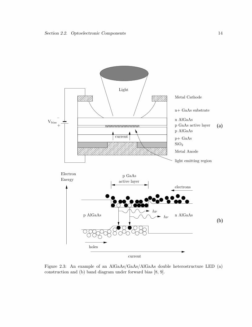
Most modern LEDs in the band of interest are constructed from GaAs and AlGaAs
as double heterostructure devices. This type of structure is formed by depositing two
wide band gap materials on either side of a lower band gap material, and doping the
materials appropriately to give diode action. An example of an AlGaAs/GaAs/AlGaAs
double heterostructure LED is illustrated in Figure 2.3. Under forward bias conditions, the
band diagram forms a potential well in the low band gap material (GaAs) into which carriers
are injected. This region is known as the active region where recombination of the injected
carriers takes place. The recombination process in the active region occurs randomly and as
a result the photons are generated incoherently (i.e., the phase relationship between emitted
photons is random in time). This type of radiation is termed spontaneous emission [8].
The advantages of using a double heterostructure stem from the fact that the
injected carriers are confined to a well defined region. This confinement results in large
concentration of injected carriers in the active region. This in turn reduces the radiative
recombination time constant, improving the frequency response of the device. Another
advantage of this carrier confinement is that the generated photons are also confined to a
well defined area. Since the adjoining regions have a larger band gap than the active region,
the losses of due to absorption in these regions is minimised [9].
Using the structure for the LED in Figure 2.3, it is possible to derive an expression
for the output optical power of the device as a function of the drive current in the following
form :
Pvol = hνJ
qdBτn
(po + no +
τnJ
qd
), (2.2)
where Pvol is the output power per unit device volume, J is the the current density ap-
plied, hν is the photonic energy, d is the thickness of the active region, B is the radiative
recombination coefficient, τn is electron lifetime in the active region and po, no are carrier
concentrations at thermal equilibrium in the active region [8].
Equation 2.2 shows that for low levels of injected current, po > τnJ/qd and Pi is
approximately proportional to the current density. As the applied current density increases
Section 2.2. Optoelectronic Components 14
(a)
(b)
electrons
ElectronEnergy
holes
current
hν
hν
p GaAsactive layer
Light
n+ GaAs substrate
p+ GaAs
Metal Anode
SiO2
+
–
current
p GaAs active layern AlGaAs
p AlGaAs
Vbias
Metal Cathode
light emitting region
p AlGaAs n AlGaAs
Figure 2.3: An example of an AlGaAs/GaAs/AlGaAs double heterostructure LED (a)construction and (b) band diagram under forward bias [8, 9].
Section 2.2. Optoelectronic Components 15
(by increasing drive current) the optical output of the device exhibits more non-linear
components. The choice of active region thickness, d, is a critical design parameter for
source linearity. By increasing the thickness of the active region, the device has a wider
range of input currents over which the behaviour is linear. However, an increase in the active
region thickness reduces the confinement of carriers. This, in turn, limits the frequency
response of the device as mentioned above. Thus, there is a trade-off between the linearity
and frequency response of LEDs.
Another important characteristic of the LED is the performance of the device due
to self-heating. As the drive current flows through the device, heat is generated due to
the Ohmic resistance of the regions as well as the inefficiency of the device. This increase
in temperature degrades the internal quantum efficiency of the device by reducing the
confinement of carriers in the active region since a large majority have enough energy
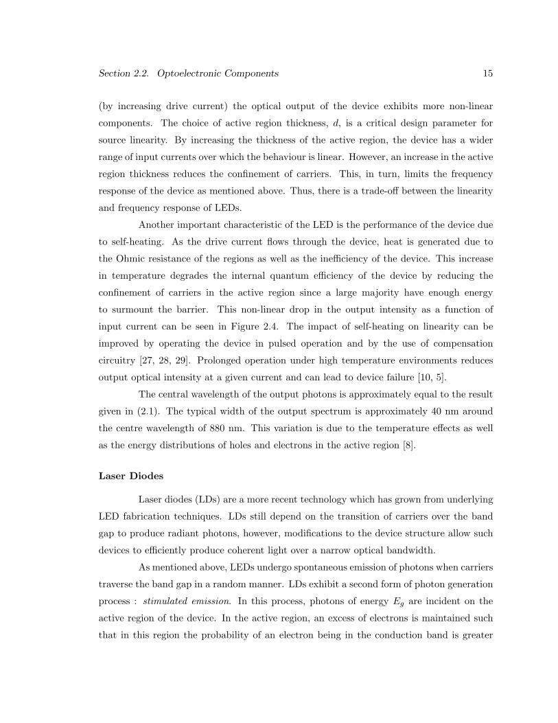
to surmount the barrier. This non-linear drop in the output intensity as a function of
input current can be seen in Figure 2.4. The impact of self-heating on linearity can be
improved by operating the device in pulsed operation and by the use of compensation
circuitry [27, 28, 29]. Prolonged operation under high temperature environments reduces
output optical intensity at a given current and can lead to device failure [10, 5].
The central wavelength of the output photons is approximately equal to the result
given in (2.1). The typical width of the output spectrum is approximately 40 nm around
the centre wavelength of 880 nm. This variation is due to the temperature effects as well
as the energy distributions of holes and electrons in the active region [8].
Laser Diodes
Laser diodes (LDs) are a more recent technology which has grown from underlying
LED fabrication techniques. LDs still depend on the transition of carriers over the band
gap to produce radiant photons, however, modifications to the device structure allow such
devices to efficiently produce coherent light over a narrow optical bandwidth.
As mentioned above, LEDs undergo spontaneous emission of photons when carriers
traverse the band gap in a random manner. LDs exhibit a second form of photon generation
process : stimulated emission. In this process, photons of energy Eg are incident on the
active region of the device. In the active region, an excess of electrons is maintained such
that in this region the probability of an electron being in the conduction band is greater
Section 2.2. Optoelectronic Components 16
spontaneousemission
spontaneousemission
stimulatedemission
3000 100 2000
2
4
6
8
Opt
ical
Pow
erE
mit
ted
(mW
)
current (mA)
LED
Laser
LED operating mode
Laser operating modes
Ithreshold
Figure 2.4: An example of an optical intensity versus drive current for LED and LD [10]
than it being in the valence band. This state is called population inversion and is created
by the confinement of carriers in the active region and the carrier pumping of the forward
biased junction. The incident photon induces recombination processes to take place. The
emitted photons in this process have the same energy, frequency, and phase as the incident
photon. The output light from this reaction is said to be coherent [8, 7, 30].
In order for this process to be sustainable, the double heterostructure is modified
to provide optical feedback. This optical feedback occurs essentially by placing a reflective
surface to send generated photons back through the active region to re-initiate the recom-
bination process. There are many techniques to provide this optical feedback, each with
their merits and disadvantages. A Fabry-Perot laser achieves photon confinement by having
internal reflection inside the active region. This is accomplished by adjusting the refractive-
index of surrounding materials. The ends of the device have mirrored facets which are
cleaved from the bulk material. One facet provides nearly total reflection while the other
allows some transmission to free-space [8].
The operation of this optical feedback structure is analogous to microwave res-
onators which confine electromagnetic energy by high conductivity metal. These structures

Section 2.2. Optoelectronic Components 17
resonate at fixed set of modes depending on the physical construction of the cavity. As a
result, due to the structure of the resonant cavity LDs emit their energy over a very narrow
spectral width. Also, the resonant nature of the device allows for the emission of relatively
high power levels.
Unlike LEDs which emit a light intensity approximately proportional to the drive
current, lasers are threshold devices. As shown in Figure 2.4, at low drive currents sponta-
neous emission dominates and the device behaves essentially as a low intensity LED. After
the current surpasses the threshold level, Ithreshold, stimulated emission dominates and the
device exhibits a high optical efficiency as indicated by the large slope in the figure. In the
stimulated emission region, the device exhibits an approximately linear variation of optical
intensity versus drive current.
Comparison
The chief advantage of LDs over LEDs is in the speed of operation. Under condi-
tions of stimulated emission, the recombination time constant is approximately one to two
orders of magnitude shorter than during spontaneous recombination [9]. This allows LDs
to operate at pulse rates in the gigahertz range, while LEDs are limited to megahertz range
operation.
The variation of optical characteristics over temperature and age are more pro-
nounced in LDs than in LEDs. As is the case with LEDs, the general trend is to have
lower radiated power as temperature increases. However, a marked difference in LDs is that
the threshold current as well as the slope of the characteristic can change drastically as a
function of temperature or age of the device. For commercial applications of these devices,
such as laser printers, copiers or optical drives, additional circuitry is required to stabilize
operating characteristics over the life of the device [31, 32].
For LDs the linearity of the optical output power as a function of drive current
above Ithreshold also degrades with device aging. Abrupt slope changes, known as kinks,
are evident in the characteristic due to defects in the junction region as well as due to
device degradation in time [10]. LEDs do not suffer from kinks over their lifetimes. Few
manufactures quote linearity performance of their devices over their operating lifetimes.
LDs are more difficult to construct and as a result can be more expensive than
LEDs. As stated in Chapter 1, the use of inexpensive optical components is a key factor

Section 2.2. Optoelectronic Components 18
Characteristic LED LDOptical Spectral Width 25–100 nm 0.1 to 5 nmModulation Bandwidth Tens of kHz to Tens of kHz to
Hundreds of MHz Tens of GHzSpecial Circuitry Required None Threshold and Temperature
Compensation CicuitryEye Safety Considered Eye Safe Must be rendered eye safeReliability High ModerateCost Low Moderate to High
Table 2.3: Comparison of LEDs versus LDs for wireless optical links (based on [4, 5])
determining the implementation of a wireless IR link.
An important limitation for the use of LDs for wireless optical applications is the
fact that it is difficult to render laser output eye safe. Due to the coherency and high
intensity of the emitted radiation, the output light must be diffused. This requires the use
of filters which reduce the efficiency of the device and increase system cost. LEDs are not
optical point sources, as are LDs, and can launch greater radiated power while maintaining
eye safety limits [4, 3].
As a result of these issues, LEDs were chosen as the light emitting devices for the
target application. The strengths and weakness of LDs and LEDs for wireless applications
are summarised in Table 2.3.
2.2.2 Photodetectors
Photodetectors are solid-state devices which perform the inverse operation of light
emitting devices : they convert the incident radiant light into an electrical current. Photode-
tectors are essentially reverse biased diodes on which the radiant optical energy is incident,
and are also referred to as photodiodes. The incident photons, if they have sufficient energy,
generate free electron-hole pairs. The drift or diffusion of these carriers to the contacts of
the device constitutes the detected photocurrent.
Inexpensive photodetectors can be constructed of silicon (Si) for the 780–950 nm
optical band. The photonic energy at the 880 nm emission peak of GaAs is approximately
Eg = 1.43 eV, by rearranging (2.1). Since the band gap of silicon is approximately 1.15 eV,
these photons have enough energy to promote electrons to the conduction band, and hence
are able to create free electron-hole pairs. Figure 2.5 shows that the sensitivity of a silicon
Section 2.2. Optoelectronic Components 19
Ultra-Violet Visible Close Infrared
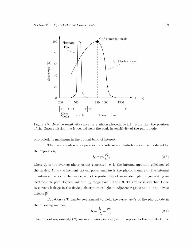
HumanEye
0
20
40
60
80
100
200 500 1000 1300λ (nm)
880
Si Photodiode
GaAs emission peak
Sens
itiv
ity
(%)
Figure 2.5: Relative sensitivity curve for a silicon photodiode [11]. Note that the positionof the GaAs emission line is located near the peak in sensitivity of the photodiode.
photodiode is maximum in the optical band of interest.
The basic steady-state operation of a solid-state photodiode can be modelled by
the expression,
Ip = qηiPp
hν, (2.3)
where Ip is the average photocurrent generated, ηi is the internal quantum efficiency of
the device, Pp is the incident optical power and hν is the photonic energy. The internal
quantum efficiency of the device, ηi, is the probability of an incident photon generating an
electron-hole pair. Typical values of ηi range from 0.7 to 0.9. This value is less than 1 due
to current leakage in the device, absorption of light in adjacent regions and due to device
defects [5].
Equation (2.3) can be re-arranged to yield the responsivity of the photodiode in
the following manner,
R =Ip
Pp=
qηi
hν(2.4)
The units of responsivity (R) are in amperes per watt, and it represents the optoelectronic
Section 2.2. Optoelectronic Components 20
intrinsicregionlayer
depletion
Metal Anode
SiO2
Anti-reflection Coating
p+ region
n+ region
hν
E
+
–Vbias
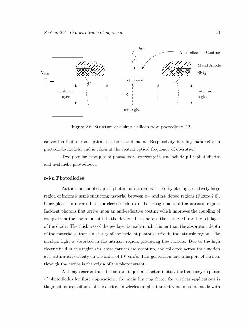
Figure 2.6: Structure of a simple silicon p-i-n photodiode [12].
conversion factor from optical to electrical domain. Responsivity is a key parameter in
photodiode models, and is taken at the central optical frequency of operation.
Two popular examples of photodiodes currently in use include p-i-n photodiodes
and avalanche photodiodes.
p-i-n Photodiodes
As the name implies, p-i-n photodiodes are constructed by placing a relatively large
region of intrinsic semiconducting material between p+ and n+ doped regions (Figure 2.6).
Once placed in reverse bias, an electric field extends through most of the intrinsic region.
Incident photons first arrive upon an anti-reflective coating which improves the coupling of
energy from the environment into the device. The photons then proceed into the p+ layer
of the diode. The thickness of the p+ layer is made much thinner than the absorption depth
of the material so that a majority of the incident photons arrive in the intrinsic region. The
incident light is absorbed in the intrinsic region, producing free carriers. Due to the high
electric field in this region (E), these carriers are swept up, and collected across the junction
at a saturation velocity on the order of 107 cm/s. This generation and transport of carriers
through the device is the origin of the photocurrent.
Although carrier transit time is an important factor limiting the frequency response
of photodiodes for fibre applications, the main limiting factor for wireless applications is
the junction capacitance of the device. In wireless applications, devices must be made with

Section 2.2. Optoelectronic Components 21
relatively large areas so as to be able to collect as much radiant optical power as possible.
As a result, the capacitance of the device can be relatively large. Additionally, the junction
capacitance is increased due to the fact that low reverse bias voltages must be used. This
is due to the fact that these devices are destined for applications in portable devices where
power consumption and hence voltage rails are minimised. Typical values for this junction
depletion capacitance at a reverse bias of 3.3 V range from 2 pF for expensive devices used
in some fibre applications to 20 pF for very low speed, and cost devices. Careful design of
receiver structures is necessary so as not to unduly reduce system bandwidth or increase
noise [33].
The relationship between generated photocurrent and incident optical power for
p-i-n photodiodes in (2.3) has been shown to be linear over six to eight decades of input
level [6, 11]. Second order effects appear when the device is operated at high frequencies
as a result of variations in transport of carriers through the high-field region. These effects
become prevalent at frequencies above approximately 5 GHz and do not limit the linearity
of links at lower frequencies of operation [34]. Since the frequency of operation is limited
due to junction capacitance, the non-linearities due to charge transport in the device are
negligible. The p-i-n photodiode behaves in a linear fashion over a wide range for the
proposed application.
Avalanche Photodiodes
The basic construction of avalanche photodiodes (APDs) is very similar to that
of a p-i-n photodiode. The difference is that for every photon which is absorbed by the
intrinsic layer, more than on electron-hole pair may be generated. As a result, APDs have
a photocurrent gain of greater than unity, while p-i-n photodiodes are fixed at unit gain.
The process by which this gain arrives is known as avalanche multiplication of
the generated carriers. A high intensity electric field is established in the depletion region.
This field accelerates the generated carriers so that collisions with the lattice generate
more carriers. The newly generated carriers are also accelerated by the field, repeating the
impact generation of carriers. The photocurrent gain possible with this type of arrangement
is of the order 102 to 104 [6, 12]. In wired fibre networks, the amplifying effect of APDs
improves the sensitivity of the receiver allowing for longer distances between repeaters in
the transmission network [9].

Section 2.2. Optoelectronic Components 22
The disadvantage of this scheme is that the avalanche process generates excess shot
noise due to the current flowing in the device. This excess noise can degrade the operation
of free space links since a majority of the noise present in the system is due to high intensity
ambient light. These noise sources are discussed in more detail in Section 2.4.
The avalanche gain is a strong non-linear function of bias voltage and temperature.
The primary use of these devices is in digital systems due to their poor linearity. Additional
circuitry is required to stabilize the operation of these devices. As a result of the overhead
required to use these devices, the system reliability is also degraded [5].
Comparison
APDs provide a gain in the generated photocurrent while p-i-n diodes generate
at most one electron-hole pair per photon. It is not clear that this gain produces an
improvement in the signal-to-noise ratio (SNR) in every case. Indeed, for the case of a free
space optical link operating in ambient light, APDs can actually provide a decrease in SNR
[23], as described in Section 2.4.
Due to the non-linear dependence of avalanche gain on the supply voltage and
temperature, APDs exhibit non-linear behaviour throughout their operating regime. The
addition of extra circuitry to improve this situation increases cost and lowers system relia-
bility. Additional circuitry is also necessary to generate the high bias voltages necessary for
high field APDs. Typical supply voltages range from 30 V for InGaAs APDs to 300 V for
silicon APDs. Since these devices are destined for portable devices with limited supplies,
APDs are not appropriate for this application.
p-i-n diodes are available at relatively low cost and at a variety of wavelengths.
They have nearly linear optoelectronic characteristics over many decades of input level.
p-i-n photodiodes can be biased from lower supplies with the penalty of increasing junction
capacitance.
Due to the issues discussed in the preceding section, a p-i-n photodiode was chosen
as the photodetector in this application. The characteristics of both p-i-n photodiodes as
well as APDs are summarised in Table 2.4.

Section 2.3. Experimental Channel 23
Characteristic p-i-n Photodiode Avalanche PhotodiodeModulation Bandwidth Tens of MHz to Hundreds of MHz to(ignoring circuit) Tens of GHz Tens of GHzPhotocurrent Gain 1 102 − 104
Special Circuitry Required None High Bias Voltages andTemperature Compensation Circuitry
Linearity High Low – suited to digital applicationsCost Low Moderate to High
Table 2.4: Comparison of p-i-n photodiodes versus avalanche photodiodes for wireless opti-cal links (based on [5, 6])
2.3 Experimental Channel
The use of LEDs and p-i-n photodiodes offer distinct advantages in implementation
ease over other optoelectronic components. However, to have a wireless infrared solution
viable for wide spread use, inexpensive optical components must be used. Additionally, since
most optical links are destined for pulsed operation, few analog measurements are available
in the literature. Notably, the linearity of optical components is typically unreported.
An experimental channel has been constructed using commercially available op-
toelectronic components. The purpose of creating an experimental channel is to determine
the impact of inexpensive optical components on system bandwidth and linearity. This
section presents the design methodology used to create the components of the link as well
as the results of measurements on the entire channel.
2.3.1 Circuit Design
As shown in Figure 2.1 on page 7, a wireless optical link consists of transmit
and receive electronics in addition to optoelectronic components. Since the goal of the
experimental link is to provide information about the linearity and bandwidth of the optical
components, care must be taken to ensure that the electronics do not limit or corrupt the
measurements.
Transmit and receive side electronics were constructed using discrete Motorola
MRF581 high-frequency bipolar transistors. The circuits were implemented on custom
designed circuit boards. The issues involved in the design of these circuits along with
measurements of the constructed circuits is presented in the subsequent sections.
Section 2.3. Experimental Channel 24
40kΩ
50Ω
10nF
50Ω
MeasurementCircuit
SpectrumAnalyzer10nF
50Ω
50Ω
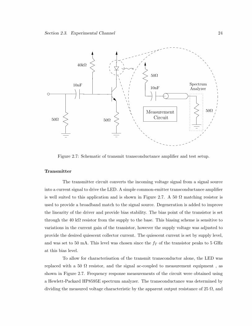
Figure 2.7: Schematic of transmit transconductance amplifier and test setup.
Transmitter
The transmitter circuit converts the incoming voltage signal from a signal source
into a current signal to drive the LED. A simple common-emitter transconductance amplifier
is well suited to this application and is shown in Figure 2.7. A 50 Ω matching resistor is
used to provide a broadband match to the signal source. Degeneration is added to improve
the linearity of the driver and provide bias stability. The bias point of the transistor is set
through the 40 kΩ resistor from the supply to the base. This biasing scheme is sensitive to
variations in the current gain of the transistor, however the supply voltage was adjusted to
provide the desired quiescent collector current. The quiescent current is set by supply level,
and was set to 50 mA. This level was chosen since the fT of the transistor peaks to 5 GHz
at this bias level.
To allow for characterisation of the transmit transconductor alone, the LED was
replaced with a 50 Ω resistor, and the signal ac-coupled to measurement equipment , as
shown in Figure 2.7. Frequency response measurements of the circuit were obtained using
a Hewlett-Packard HP8595E spectrum analyzer. The transconductance was determined by
dividing the measured voltage characteristic by the apparent output resistance of 25 Ω, and

Section 2.3. Experimental Channel 25
100 200 300 400−60
−55
−50
−45
−40
(a)
Frequency (MHz)
Tra
nsco
nduc
tanc
e G
ain
(dB
)
50 100 150 200 250 300 350−70
−60
−50
−40
−30
−20
−10
0(b)
Frequency (MHz)
Out
put P
ower
(dB
c)
Figure 2.8: Measurement results of transmit transconductor : (a) frequency response and(b) harmonic distortion.
the plot in Figure 2.8 was generated. The harmonic distortion of the circuit was measured
by applying a 0 dBm tone at 100 MHz at the input of the transconductor from a Rhode &
Schwartz RF generator (5 kHz-3 GHz). The resulting spectrum at the output was captured
by the HP8595E, and is also illustrated in Figure 2.8. The measured harmonic content
of the RF generator output alone showed that the second harmonic was 35 dB below the
fundamental for the test tone applied.
The measurements indicate that the circuit provides a nearly constant transcon-
ductance of -40 dBf in a frequency range from 1 MHz to 300 MHz. The harmonic distortion
of the circuit is better than approximately 35 dB and measurement is limited by the dis-
tortion of the signal source.
Receiver
The receive electronics amplify the received photocurrent signal and buffer the
output to drive measurement equipment. The pre-amplifiers of the receive stage are critical
components in any system design. As is the case in any receive chain, the front-end architec-
ture is most important in determining the noise performance of the entire chain. A variety
of amplifier techniques and topologies are available to provide low noise operation [35, 33].
The goal of the pre-amplifier for this application is to emphasize frequency response and
linearity over noise performance of the circuit to allow for unhindered characterisation of
these two parameters.

Section 2.3. Experimental Channel 26
The receive amplifier, as shown in Figure 2.9, ac-couples the incoming photocur-
rent, allowing only the signal portion to enter the amplifier. The front end stage, consisting
of Q1 and feedback network, forms a transimpedance input stage. This type of topology
provides a good compromise between low noise characteristic and high bandwidth implemen-
tation. Transimpedance amplifiers are commonly used in optical receiver design [36, 37, 33].
Placing decoupling around Rf1 allows the DC bias of Q1 to be specified independently of
its AC gain. This stage can be thought of as converting the current signal to a voltage
signal and provides a gain of approximately 700 Ω at midband frequencies. Q2 forms the
heart of a common emitter amplifier which provides a modest voltage gain. The frequency
response of the amplifier is improved by the addition of compensation elements Re2 and
Ce2. It is possible to show that the compensation components add a zero in the amplifier
transfer characteristic at ωz = 1/Re2Ce2 rad/s. By careful design, this zero can be used to
cancel the dominant pole of the first stage determined by Rf2 and the Cµ of Q1. For the
final design, Re2 was set by bias and linearity issues and Ce2 was estimated and optimised
iteratively in hardware. Q3 buffers the voltage output of the previous stage and presents a
matched load to the measurement device.
As in the transmitter, circuit techniques were employed to allow for the measure-
ment of the circuit parameters without optoelectronic components. A small signal current
source was constructed on the same circuit board as the transimpedance amplifier, and is
also shown in Figure 2.9. This circuit provides a matched load to the signal source and uses
the 20 kΩ resistor to approximate voltage independence with current.
The same test equipment was used to characterise the receive amplifier as were
used for the transmit amplifier. The supply voltage was set to 20 V, to improve the linearity
of the amplifier (due to increased VCB) and to allow for reasonably sized resistors for the
bias currents required for maximum fT . Using the same input signals as in the transmitter
case, the frequency response and harmonic distortion were measured and are presented in
Figure 2.10. The transimpedance gain is obtained from the voltage gain of the amplifier by
approximating the input current to be iin ≈ vin/40kΩ.
The measured values indicate that the transimpedance receiver provides a gain of
approximately 61 dBΩ over a range from 1 MHz to 350 MHz. The linearity of the amplifier
is better than 35 dB and is limited by the harmonic distortion present in the source, as was
the case in the transmitter.

Section 2.3. Experimental Channel 27
50Ω
50Ω
20kΩ
iphoto
CircuitMeasurement
1kΩ10pF
Q1
Q3
Q2
10nF
750Ω
135Ω
50Ω
20Ω220Ω320Ω
iphoto
10nF 10nF
Vsrc
5kΩRf1
Rf2
60Ω
Re2
Ce2
Figure 2.9: Schematic of receive transimpedance amplifier and test setup.

Section 2.3. Experimental Channel 28
100 200 300 400 5000
20
40
60
80(a)
Frequency (MHz)
Tra
nsim
pede
nce
Gai
n (d
BΩ)
50 100 150 200 250 300 350
−40
−30
−20
−10
0(b)
Frequency (MHz)
Out
put P
ower
(dB
c)
Figure 2.10: Measurement results of receive transimpedance amplifier : (a) frequency re-sponse and (b) harmonic distortion.
2.3.2 Channel Measurements
The test circuits used to characterise receiver and transmitter were replaced with
optoelectronic components to determine their linearity and frequency response. A Mitel
1A301 LED [38] and a Temic BPV10NF [39] silicon p-i-n photodiode were chosen as test
subjects representative of current optoelectronics. The Mitel LED is designed for 266 Mbps
fibre links, and has a reported bandwidth of 350 MHz. The Temic photodiode is reported as
having a bandwidth of 100 MHz, however, the measurement method is not well documented.
The suggested applications for this photodiode are for 450 kHz/1.3 MHz FSK remote control
purposes as well as 4 Mbps IrDA links (as described in Chapter 1).
The optoelectronic devices were soldered onto the circuit boards and the test
circuits were removed from the signal path. The boards were mounted in a test fixture, as
shown in Figure 2.11, the LED and photodiode where aligned by hand and the distance
between then adjusted to 1.5 cm.
At the transmitter, the bias for the LED was set at 50 mA, since this is in the
middle of the range of allowed currents for the Mitel component. The reverse bias across
the photodiode was set at 20 V. According to the data sheet [39], this should place the
depletion capacitance near 2.5 pF. The reverse bias was set to a high level to limit the
deletion capacitance. In this manner, the time constant due to photodiode capacitance and
the input impedance of the receive amplifier is pushed to a higher frequency. This was done
Section 2.3. Experimental Channel 29
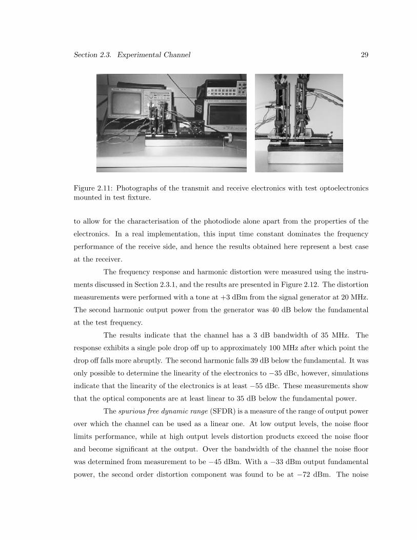
Figure 2.11: Photographs of the transmit and receive electronics with test optoelectronicsmounted in test fixture.
to allow for the characterisation of the photodiode alone apart from the properties of the
electronics. In a real implementation, this input time constant dominates the frequency
performance of the receive side, and hence the results obtained here represent a best case
at the receiver.
The frequency response and harmonic distortion were measured using the instru-
ments discussed in Section 2.3.1, and the results are presented in Figure 2.12. The distortion
measurements were performed with a tone at +3 dBm from the signal generator at 20 MHz.
The second harmonic output power from the generator was 40 dB below the fundamental
at the test frequency.
The results indicate that the channel has a 3 dB bandwidth of 35 MHz. The
response exhibits a single pole drop off up to approximately 100 MHz after which point the
drop off falls more abruptly. The second harmonic falls 39 dB below the fundamental. It was
only possible to determine the linearity of the electronics to −35 dBc, however, simulations
indicate that the linearity of the electronics is at least −55 dBc. These measurements show
that the optical components are at least linear to 35 dB below the fundamental power.
The spurious free dynamic range (SFDR) is a measure of the range of output power
over which the channel can be used as a linear one. At low output levels, the noise floor
limits performance, while at high output levels distortion products exceed the noise floor
and become significant at the output. Over the bandwidth of the channel the noise floor
was determined from measurement to be −45 dBm. With a −33 dBm output fundamental
power, the second order distortion component was found to be at −72 dBm. The noise
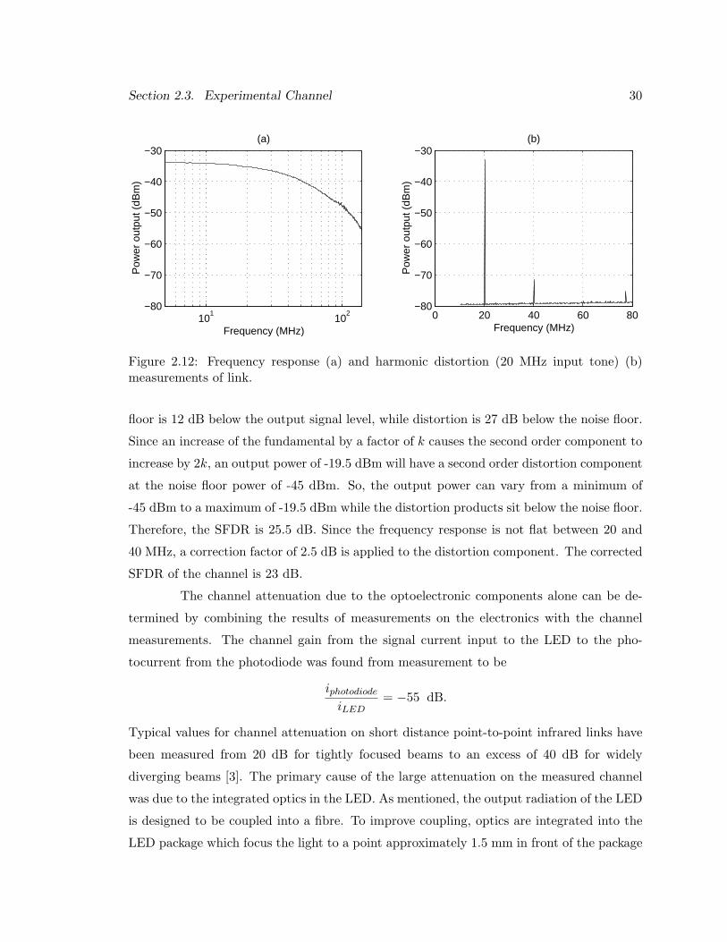
Section 2.3. Experimental Channel 30
0 20 40 60 80−80
−70
−60
−50
−40
−30(b)
Frequency (MHz)
Pow
er o
utpu
t (dB
m)
101
102
−80
−70
−60
−50
−40
−30(a)
Frequency (MHz)
Pow
er o
utpu
t (dB
m)
Figure 2.12: Frequency response (a) and harmonic distortion (20 MHz input tone) (b)measurements of link.
floor is 12 dB below the output signal level, while distortion is 27 dB below the noise floor.
Since an increase of the fundamental by a factor of k causes the second order component to
increase by 2k, an output power of -19.5 dBm will have a second order distortion component
at the noise floor power of -45 dBm. So, the output power can vary from a minimum of
-45 dBm to a maximum of -19.5 dBm while the distortion products sit below the noise floor.
Therefore, the SFDR is 25.5 dB. Since the frequency response is not flat between 20 and
40 MHz, a correction factor of 2.5 dB is applied to the distortion component. The corrected
SFDR of the channel is 23 dB.
The channel attenuation due to the optoelectronic components alone can be de-
termined by combining the results of measurements on the electronics with the channel
measurements. The channel gain from the signal current input to the LED to the pho-
tocurrent from the photodiode was found from measurement to be
iphotodiode
iLED= −55 dB.
Typical values for channel attenuation on short distance point-to-point infrared links have
been measured from 20 dB for tightly focused beams to an excess of 40 dB for widely
diverging beams [3]. The primary cause of the large attenuation on the measured channel
was due to the integrated optics in the LED. As mentioned, the output radiation of the LED
is designed to be coupled into a fibre. To improve coupling, optics are integrated into the
LED package which focus the light to a point approximately 1.5 mm in front of the package

Section 2.4. Noise 31
Measurement Value Unit3 dB Bandwidth 35 MHzSecond OrderHarmonic Distortion -39 dBcSFDR 23 dBChannel Attenuation 55 dB
Table 2.5: Measurement results of experimental free-space optical link.
[38]. As the distance increases beyond this point, the radiation pattern diverges rapidly.
As a result, most the the launched power from the LED is dispersed to the environment
before arriving at the photodiode. This LED was chosen since most present-day high-speed
optoelectronic devices are destined for fibre applications. With the expansion of the wireless
optical communication market, this trend is expected to change.
Table 2.5 presents a summary of the results of channel measurements as well as
derived quantities based on those measurements.
2.4 Noise
Along with specifications regarding the frequency and distortion performance, the
noise sources of a wireless optical link are critical factors in determining performance. The
determination of noise sources at the input of the receiver is necessary since this is the
location where the incoming signal contains the least power.
As was justified in Section 2.2.2, p-i-n photodiodes are commonly used as pho-
todetectors for wireless infrared links. The two primary sources of noise at the receiver
front end are due to noise from the receive electronics and shot noise from the received DC
photocurrent.
As is the case with all electronics, noise is generated due to the random motion
of carriers in resistive and active devices. A major source of noise is thermal noise due to
resistive elements in the pre-amplifier. If a low resistance is used in the front end to improve
the frequency response, an excessive amount of thermal noise is added to the photocurrent
signal. Transimpedance pre-amplifiers provide a low impedance front end through negative
feedback and represent a compromise between these constraints [33]. Thermal noise is
generated independently of the received signal and can be modelled as having a Gaussian
Section 2.4. Noise 32
distribution. This noise is shaped by a transfer function dependent on the topology of the
pre-amplifier once the noise power is referred to the input of the amplifier. As a result, the
noise due to the circuit follows a Gaussian distribution, but it is generally non-white [4].
Photogenerated shot noise is a major noise source in the wireless optical link. This
noise is fundamentally due to the discrete nature of energy and charge in the photodiode.
Carrier pairs are generated randomly in the space charge region due to the incident photons.
Furthermore, carriers traverse the potential barrier of the p-n junction in a random fashion
dependent on their energy. The probabilistic generation and transport of carriers due to
quantum effects in the photodiode gives rise to shot noise in the photocurrent. This random
process can be modelled as a having Poisson distribution with a white power spectral density
[33, 40].
Using these two sources of noise, the signal-to-noise ratio for a wireless optical link
can be approximated in a simple example (based on [35]). The input signal to the receiver
is a time varying optical intensity signal. Let the transmitted intensity signal, x(t), be a
fixed sinusoid of the form
x(t) = Pt(1 + m sinωt)
where Pt is the average transmitted power and m is the amplitude of the sinusoid. To
ensure transmission of this signal requires |m| < 1, since negative intensity values are not
possible as discussed in Section 2.1.
This intensity signal is attenuated as it propagates through free-space to the receive
side. The received signal also consists of ambient, background light that is present in the
channel and detected by the photodiode. This ambient light consists of incandescent light,
natural light and other illumination in the environment. The received intensity, r(t), can
be written as
r(t) = Pr(1 + m sinωt) + Pamb,
where Pr is the average power at the receive side and Pamb is the power of the ambient light
incident on the photodiode. The photodiode converts this incident optical intensity into a
photocurrent in accordance with the responsivity relationship in (2.4). The signal and DC
quantities of the photocurrent can be isolated in the following form :
iphoto(t) = R · r(t) = R(Pr + Pamb) + (RPrm sinωt).
The electrical signal power at the receive side is contained entirely in the time varying
Section 2.4. Noise 33
component and can be written as
Psignal =12m2(RPr)2.
The noise power due to the pre-amplifier and due to shot noise is uncorrelated,
and so the total noise power is simply the sum of the individual noise source powers. If the
noise power due to the circuit is i2circ, the total noise power takes the form
Pnoise = i2circ + i2shot = i2circ + 2qR(Pr + Pamb)Beff ,
where q is the electronic charge and Beff is the equivalent noise bandwidth of the system.
Combining the results, an estimate of the signal-to-noise ratio of the system can be formed
as
SNRlink =Psignal
Pnoise=
12· m2(RPr)2
i2circ + 2qR(Pr + Pamb)Beff
. (2.5)
The dominant source of noise in a wireless optical channel is due to the ambient
background light. To reduce the impact of ambient light, optical low-pass filtering can be
used to attenuate visible and higher frequency light sources with little added cost [24]. In
some links, this ambient light may be as much as 25 dB greater than the signal power, even
after optical filtering [23]. The high ambient light levels cause the ambient light shot noise
component to dominate the circuit noise, allowing (2.5) to be simplified to
SNRlink ≈ m2(RPr)2
4qRPambBeff.
Using this assumption, the resulting noise of the channel is signal independent, white shot
noise following a Poisson distribution. This high intensity shot noise is the result of the
summation of many independent, Poisson distributed random variables. In the limit, as the
number of random variables summed approaches infinity, the cumulative distribution func-
tion approaches a Gaussian distribution by the central limit theorem. Thus, the dominant
noise source can be modelled as being white, signal independent and having a Gaussian
distribution [41, 40, 4].
This situation is in contrast to optical fibres where the ambient light is essentially
zero, and circuit noise is the dominant noise factor [35, 41]. The use of an APD is advanta-
geous in fibre applications as long as the circuit noise is much greater than the added shot
noise of the APD. In this manner, APDs can provide a gain to the signal portion of the
received power while keeping the noise power essentially constant. The net effect is to allow
for wider repeater spacing in a fibre network, reducing system cost [9].
Section 2.5. Summary of Characteristics and Conclusions 34
Emissions from fluorescent lighting create a noise source unique to wireless optical
channels. Fluorescent lamps have strong emissions at the spectral lines of argon in the 780–
950 nm near infrared band. Although economical narrow band optical filters have been used
for some time in such links [24], significant energies are still detected by the photodiode. The
detected output of fluorescent lamps is nearly deterministic and periodic with components
at multiples of the ballast drive frequency. Most fluorescent ballasts drive the lamps at
the line frequency of 50–60 Hz, with harmonics up to tens of kilohertz. Modern ballasts
modulate the lamp at higher frequencies to improve power efficiency and reduce unit size.
Typical modulation rates are 22 kHz and 45 kHz. The harmonics generated by these sources,
and detected by the photodiode extend into the hundreds of kilohertz and can present an
impediment to wireless optical data transmission. The impact of periodic interference from
high frequency modulated fluorescent light sources has only recently been investigated for
wireless optical links [42, 4, 23]. In this work it is assumed that the additive white noise
is dominant over fluorescent light interference. However, the robustness of certain key
modulation schemes against fluorescent light sources is briefly discussed in Chapter 3.
2.5 Summary of Characteristics and Conclusions
LEDs and p-i-n diodes are economical and practical optoelectronic components for
implementing wireless optical links. They remain reliable over a long lifetime, and require
no additional support circuitry to guarantee operation. The disadvantages of these devices
over other optoelectronic components is their slower frequency response as well as lower
efficiency.
Measurements on an experimental link were performed to characterise linearity
and frequency response using typical optical components. The measured second harmonic
distortion was better than 35 dB, and measurement was limited by the test setup. The
linear range of operation can be extended using circuit techniques [27, 28, 29], or by using
more expensive higher linearity components. These results tend to suggest that sufficient
linearity is present to allow distortion-free analog transmission over a practical range. As a
result, transmission need not be constrained to baseband digital techniques. The bandwidth
of the link was measured to be approximately 35 MHz. In order to support higher data rates,
bandwidth efficient techniques must be investigated to exploit the available bandwidth.

Section 2.5. Summary of Characteristics and Conclusions 35
The noise corrupting the input signal is due to high intensity shot noise due to am-
bient light impinging on the photodiode. This noise can be modelled as signal independent,
additive, white Gaussian noise. Low pass interference is also present due to the modulation
of ballasts in fluorescent lighting fixtures. The impact of this low pass interferer depends
heavily on system architecture and on the modulation scheme used.
Chapter 3
Modulation Schemes
The development of a high data rate wireless optical data link using inexpensive
components requires the use of efficient system level concepts to overcome the limitations
of the optoelectronics. The modulation scheme selected for such a link must satisfy all the
channel constraints while providing a high bandwidth and power efficiency. In order to
reduce the cost of the system, the scheme must be highly efficient for a relatively modest
complexity.
This chapter reviews the constraints of the wireless optical channel, and casts
them in a more formal light. After a channel model is described for the analysis of modu-
lation schemes, critical measures of performance are defined. These tools are then used to
analyse popular binary level modulation schemes for wireless optical channels. The need
for higher bandwidth efficiency leads to an investigation of multilevel modulation schemes.
We propose a new modulation scheme, adaptively biased QAM, which improves upon the
power efficiency of other multilevel schemes, while providing greater bandwidth efficiency
than binary level techniques. The chapter concludes with a comparison of the modulation
schemes considered and a discussion of the appropriateness of each scheme.
3.1 Definitions
This section reviews the characteristics of the wireless optical channel described
in earlier chapters. A simple model for the communication system is outlined, and used in
the balance of the chapter as a reference for the analysis of candidate modulation schemes.
The measures used to determine the performance of the modulation scheme are also defined
36
Section 3.1. Definitions 37
and contrasted to similar measures for conventional channels.
3.1.1 Channel Characteristics
Wireless optical links transmit information in the form of an optical intensity sig-
nal. Optoelectrical conversion is ideally linear, and produces an intensity waveform propor-
tional to the electrical signal. Due to the limitations of the optoelectronics, direct detection
of the radiant energy is performed at the receiver, rather than heterodyning techniques as
in microwave links. Since the information transmitted in the free-space channel is a power
signal, negative amplitude values are impossible. If x(t) is taken to represent the time vary-
ing optical intensity signal in the free-space channel, this non-negativity constraint can be
compactly written as
x(t) ≥ 0, ∀ t ∈ R. (3.1)
This implies that any intensity modulation scheme for the wireless infrared channel must
have a DC component which transmits no information, but consumes power.
Since the wireless infrared channel shares the same space as the user environment,
eye safety requirements impose further constraints. For time varying signals, the average
optical power transmitted must be limited. Since the signal is a time-varying intensity, eye
safety imposes a limit on the average amplitude of all signals in the channel. If the average
optical power allowed in the channel is P , the constraint due to eye safety considerations is
limT→∞
12T
∫ T
−Tx(t)dt ≤ P. (3.2)
The channel measurements in Chapter 2, indicate that inexpensive optoelectronic
devices for free-space communication have bandwidths in the 35 MHz range. Optoelectron-
ics destined for wireless communications are soon expected to provide bandwidths on the
order of several hundred megahertz. In order to implement high data rate links, approach-
ing 1 Gbps, bandwidth efficient modulation schemes must be investigated. Unlike fibre
systems, in which higher cost devices are used and in which the underlying medium has
thousands of gigahertz of available bandwidth, wireless optical links are constrained both
by low cost and by low bandwidth.

Section 3.1. Definitions 38
R n(t)
ModulatorVector
TransmitterSourceInformation Unit Energy
Matched FilterBank
Estimator
mi si(t) z(t)si
kTs
z m
Figure 3.1: A conceptualised communication model of the wireless optical link for an isolatedpulse si(t) (following [13]).
3.1.2 System Model
In order to compare various modulation schemes for wireless optical links, a sim-
plified model of the communication system was formed. Figure 3.1 graphically shows the
transmitter, channel and receiver representations, as well as the signals at various points.
At the transmitter, an information source outputs a message at a rate of Rs = 1/Ts
symbols per second. The message sent during a symbol interval is chosen as one of the M
elements in the alphabet M = m1,m2, . . . ,mM. Messages are sent independently of each
other, and the messages are selected from the alphabet with an equal probability of 1/M .
The vector transmitter accepts the generated message and performs a one-to-one
mapping between the set of messages and a set of vectors, Ω, in an N -dimensional Euclidean
space. The set of all vectors corresponding to transmitted messages, Ω, is known as the
constellation of the modulation scheme. Thus, message mi input to the vector transmitter
generates an N dimensional constellation vector si, where
si =
ai1
ai2
...
aiN
. (3.3)
The modulator converts the constellation point si into a continuous time waveform.
In the case of a wireless optical link, the vector is converted into a time varying optical
intensity. This operation is accomplished by taking the inner product of si with the set of

Section 3.1. Definitions 39
orthonormal basis functions Φ, where
Φ =
φ1(t)
φ2(t)...
φN (t)
.
The φi(t) are a set of real valued functions, time limited to t = [0, Ts]. They are determined
by the modulation scheme and must be set so that the constraints of the channel are met.
The set of φi(t) basis functions are conventionally chosen to be orthonormal, satisfying the
constraint,∫ Ts
0φk(t) · φl(t) dt =
1 : k = l
0 : k 6= l.
For message mi, the modulator outputs a time-limited optical intensity pulse, si(t), deter-
mined as
si(t) = 〈si,Φ〉 =N∑
k=1
aikφk(t), (3.4)
where the operation 〈·, ·〉 is the inner product between two vectors. The collection of the
individual si(t) symbol pulses sent over all symbol periods form the transmitted signal on
the link, defined earlier as x(t). Explicitly, x(t) takes the form
x(t) =∞∑
k=−∞sik(t− kTs) (3.5)
where sik(t) is the symbol pulse at symbol interval k, as chosen by the information source.
The symbol pulse then propagates through the free-space channel. The channel is
modelled as having a very wide bandwidth, to simplify the comparison of various schemes,
as is customary in other analyses of wireless optical modulation schemes [4, 23, 43]. The
optical intensity signal is converted to the electrical domain by the factor R which represents
the responsivity of the photodiode, defined in Chapter 2. The signal is corrupted by additive
white Gaussian noise of zero mean and two sided power spectral density of σ2n at the front-
end of the receiver.
The corrupted symbol pulse at the receiver, z(t), is detected using a bank of
N unit energy matched filters. These filters are matched to the φi(t) basis functions.
Assuming perfect timing synchronisation, the symbol rate sampled output of the matched
filters produces an N -dimensional vector z = si + n where the noise vector, n, is composed
Section 3.1. Definitions 40
of N independent discrete Gaussian random variables of zero mean and variance σ2n. Unit
energy matched filters are used to ensure that for all modulation schemes investigated, the
variance of the discrete Gaussian random variables is the same. It is well known, that the
received vector contains sufficient statistics to form an estimate of the sent message [13].
An estimate of the sent symbol, m, is formed based on the received vector z. Since
the source outputs all the symbols with equal probability, maximum likelihood (ML) rules
can be used to detect the sent symbol. Since the likelihood function
fz|mi sent = (2πσ2n)−N/2 exp(‖z− si‖2/2σ2
n),
the ML detector assigns m = mi, for the the i which minimises the Euclidean distance
criterion ‖z−si‖2. In this manner, maximum likelihood decoding is equivalent to minimum-
distance decoding [13].
3.1.3 Relating Channel Constraints to the Signal Space
The model of the wireless optical channel in Section 3.1.2 is useful in determining
the error performance of a given modulation scheme in the presence of additive white
Gaussian noise. The model, however, does not represent the fundamental constraints of the
wireless optical channel described in (3.1) and (3.2). The essential trade-offs in the design
of modulation schemes for wireless optical channels depend on the relationship between
the optical channel constraints and the properties of the signal space, which determine the
probability of symbol error.
The decoding process involves searching the constellation and computing the Eu-
clidean distance between the received message point and each constellation point. The
constellation point closest to the received point is taken as the estimate of the received
symbol. An error in decoding occurs if m 6= mi, when mi is sent. This decoding process
suggests that the distance between constellation points in the signal space determines the
probability of error for a given modulation scheme. The squared Euclidean distance, d2,
between any two constellation points in the signal space, si and sj, can be written as,
d2 = ‖si − sj‖2 =N∑
k=1
(aik − ajk)2. (3.6)
where the aik are the vectorial components as defined in (3.3).

Section 3.1. Definitions 41
Equation 3.4 demonstrates the link between the coordinates in the signal space
and the time domain intensity functions, si(t). The channel imposes constraints on these
time domain functions, which can then be related to the signal space model.
The non-negativity constraint in (3.1) is imposed on the infinite extent intensity
function, x(t) defined in (3.5). According to this definition of x(t), each of the si(t) must
be transmittable in isolation which requires si(t) ≥ 0 within the symbol period 1. Using
(3.4), the non-negativity constraint can be written as
si(t) =N∑
k=1
aikφk(t) ≥ 0 (3.7)
for t ∈ [0, Ts].
In a similar fashion, the average optical power constraint of (3.2) can also be
written in terms of the vectorial components of the constellation points. P is related to the
transmitted symbols through the set of functions si(t) defined in (3.4). Since the symbols are
equiprobable, the average optical power is the expected value over all of the time averages
of the si(t). Formally,
P =1M
M∑
i=1
1Ts
∫ Ts
0si(t) dt
=1M
M∑
i=1
N∑
k=1
aik1Ts
∫ Ts
0φk(t) dt
=1M
M∑
i=1
N∑
k=1
aikφk(t), (3.8)
where φk(t) is the average value of the basis function within a symbol period. The implica-
tion of (3.8) can be demonstrated by considering the variation of the aik with P for a fixed
set of basis functions. Following (3.8), the average optical power P is proportional to every
aik with the same proportionality constant. For example, an increase in P by a factor of
K, implies that each aik also increases by a factor of K, since the φk(t) are fixed. Applying
this fact to (3.6), shows that d2 ∝ P 2. Therefore, d ∝ P , where P is the average optical
power transmitted on the link.
The channel constraints in signal space domain provide a set of relationships be-
tween the coordinates of the constellation points for any intensity modulated channel. These1Chapter 4 addresses the case when the si(t) overlap in time and are not necessarily transmittable in
isolation.
Section 3.1. Definitions 42
relationships can be simplified by noticing that the function φavg(t), defined as
φavg(t) =√
1Ts
rect(
t− Ts/2Ts
)(3.9)
where,
rect(t) =
1 : |t| ≤ 1/2
0 : otherwise
can be chosen as a basis function for every intensity modulation technique. This basis
function represents the average value added to each symbol. The non-negativity constraint
ensures that all non-zero symbols transmitted must have a DC component. Defining φavg(t)
as a basis function, ensures the average of all other basis functions in [0, Ts], is zero due to
the orthogonality of the basis functions.
For notation’s sake, let φ1(t) = φavg(t). The non-negativity constraint in (3.7) can
be simplified as
ai11√Ts≥ −
N∑
k=2
aikφk(t)
for t ∈ [0, Ts]. It is enough to have this expression satisfied at the value of t where the
summation is minimised, since by definition all other points are more positive. Additionally,
since the right hand side of the inequality consists of functions with zero average value, the
minimum value will always be less than or equal to zero. As a result, we can write
ai11√Ts≥ − min
t∈[0,Ts]
N∑
k=2
aikφk(t)
, (3.10)
which states that the DC bias added to each symbol must at least be equal in magnitude
to the maximum negative excursion of the signal components which vary inside the symbol
period.
The average power constraint in (3.8) can also be simplified by noting that
φi(t) = 0 , i > 1.
The simplified expression takes the form,
P =1M
M∑
i=1
ai1φ1(t)
=1M
M∑
i=1
ai11√Ts
. (3.11)
Section 3.1. Definitions 43
Substituting (3.10) gives,
P ≥ − 1M
M∑
i=1
mint∈[0,Ts]
N∑
k=2
aikφk(t)
.
Let Pexi ≥ 0 be the excess power added to symbol i above the minimum required by (3.10).
The expression for the average power constraint can then be written as an equality in the
form
P − 1M
M∑
j=1
Pexj = − 1M
M∑
i=1
mint∈[0,Ts]
N∑
k=2
aikφk(t)
. (3.12)
For a given set of φi(t) and P , the average value is set by the choice of excess power and
vector coordinates aik. The power term on the left hand side of (3.12) fixes the negative
peak values of the symbol functions represented on the right hand side. Minimisation of the
excess power allows larger negative amplitude values for the symbols, or equivalently larger
aik values. Although large values for the aik do not guarantee better separation of signal
points, they increase the size of the region in signal space in which constellation points can
be placed while satisfying the channel constraints. Thus, for a given modulation scheme
defined by a set of φi(t), the minimisation of excess optical power increases the the region in
signal space where constellation points can exist for a given P , which in turn can potentially
lead to an increase in spacing between signal points.
This coincides with intuition, since the excess power transmitted does not transmit
any information and consumes a larger than necessary part of the average power budget.
Power efficient schemes should then transmit zero excess power per symbol to allow for
larger values of aik which in turn provides a greater degree of flexibility in choosing points
from the signal space.
It must be noted that (3.12) is highly dependent on the structure of the φi(t)
through the minimisation term. Further generalisation is difficult since the aik are con-
strained not only by the channel but also by the choice of basis functions. As a result, the
expression for a distance in the signal space in (3.6) is not only dependent on the average
power P , but is dependent on the pulse shapes of the φi(t) due to the channel constraints.
3.1.4 Definition of Measures
In order to compare modulation schemes on the intensity modulated channel,
figures of merit must be specified which encapsulate the performance of each technique. Key
Section 3.1. Definitions 44
figures of merit are measures that illustrate the power efficiency and bandwidth efficiency
of the modulation scheme in light of the channel constraints.
Probability of Error
The estimation of the probability of a symbol error occurring in the detection
process is a key parameter of any modulation scheme. The probability of symbol error
is defined as, Pe(sym) = Prm 6= mi | mi sent. In practice, this quantity is difficult to
calculate exactly, and bounds are used to estimate its value. Where the probability of
symbol error cannot be calculated exactly, the following union bound approximation on the
probability of error is used
Pe(sym) ≈ Kmin ·Q(
dmin
2σn
), (3.13)
where dmin is the minimum Euclidean distance between two points in the signal constel-
lation, Kmin is the average number of constellation points dmin away from any point, and
Q(x) ∆= 1√2π
∫∞x exp(−z2/2)dz. In the comparison of various modulation schemes, the prob-
ability of bit error, Pe, is a figure of merit. Pe can be determined from Pe(sym) exactly in
some cases, while approximations must be made in others. A common approximation is that
Gray coding is used between adjacent symbols in the constellation. In this way, a symbol
error is with high probability associated with a single bit error. Using this approximation,
for an alphabet size of M , Pe ≈ Pe(sym)/ log2 M .
Constellation Figure of Merit
In a conventional scheme, the amount of electrical power that can be sent on the
channel is limited. It is possible to show that in this case d2min is proportional to the
electrical power of the symbols sent [41]. Improvements in Pe can be made by increasing
the transmitted electrical power, thereby increasing dmin. However, in a wireless optical
system, the limitation is not on the electrical power, but on the average optical power. Since
the relationship between optical power (or intensity) and electrical amplitude is linear, the
channel limitation translates to a constraint on the signal amplitude. Section 3.1.3 shows
that the distance between signal points in the constellation is proportional to the average
optical power. Therefore by extension, in an optical intensity channel dmin ∝ P .
In conventional channels, a key measure is the constellation figure of merit (CFM)
[44]. The constellation figure of merit is used to categorise the energy efficiency of a mod-
Section 3.1. Definitions 45
ulation scheme, and is defined as the ratio CFM ∆= d2min/E, where E is the average energy
of the constellation. This quantity is dimensionless, and independent of the pulse shape or
scaling.
In an intensity modulated channel a similar measure can be established. The
constellation figure of merit in an optical channel can be defined as
CFM =dmin
P. (3.14)
The CFM is scale invariant in terms of the transmitted optical power, since dmin ∝ P .
However, unlike the CFM defined for the conventional channel, the optical CFM is not
unitless, but suffers from a mismatch of electrical and optical quantities. The optical CFM
depends on the structure of the pulses used for a given modulation scheme as well as the
average power as discussed in Section 3.1.3.
Using the definition of CFM in (3.14), the probability of symbol error defined in
(3.13) can then be re-written as
Pe(sym) ≈ Kmin ·Q(
CFM · P2σn
).
For conventional channels corrupted by Gaussian white noise, the ratio of the
CFMs for different modulation schemes is used to compare their relative electrical energy
efficiency. It can be shown that in a conventional channel for two modulation schemes,
denoted 1 and 2, that CFM1/CFM2 is the factor improvement in electrical signal-to-noise
ratio due to the use of modulation scheme 1 over 2, for the same Pe(sym) and noise power
[45].
An analogous quantity can be computed for optical intensity channels corrupted
by Gaussian white noise. Using the definition of optical CFM in (3.14), the gain of optical
modulation scheme 1 over 2 is given as
Γ1/2 = 10 log10
CFM1
CFM2dB, (3.15)
where Γ1/2 is the gain for using modulation scheme 1 over 2. The meaning of this expression
can be simplified using (3.13), which contains an expression for the probability of symbol
error. For cases where the Pe(sym) approaches zero, the Kmin term becomes less significant
than the exponential Q(·) function, and the probability of error can be thought to depend
on dmin and σ2n alone. So, in this case, if the two modulation schemes have the same
Section 3.1. Definitions 46
probability of error and noise variance, then the dmin for both schemes is approximately
the same. Applying this simplification to (3.15) gives,
Γ1/2 = 10 log10
P2
P1dB (3.16)
where P1, P2 are the average optical power transmitted in modulation scheme 1 and 2
respectively. Therefore the gain Γ is equal to the number of decibels savings in average
optical transmit power required for scheme 1 over scheme 2 for the same noise power and
probability of symbol error.
It must be noted that the gain values are in terms of the received average optical
power and not in terms of electrical quantities. As noted earlier, dmin ∝ P in optical
channels and d2min ∝ E in electrical channels, where E is the average pulse electrical energy
for the constellation. Therefore, the gain in (3.16), in decibels, is a factor of 0.5 less than
the comparable measure in the electrical domain. For example, a Γ = 3 dB corresponds to
an increase in the electrical signal-to-noise ratio (SNR) by 6 dB.
The optical CFM is calculated for each modulation scheme considered here and is
used to perform comparisons on the relative optical power efficiency of the schemes.
Spectral Characteristics
The frequency characteristics of the transmitted modulation scheme must also be
considered. For a wide-sense stationary or wide-sense cyclostationary random process it is
possible to define a quantity called the power spectral density (psd). The psd is an averaged
second order statistic of a random process, and gives insight on the distribution of power over
frequency. As discussed in Chapter 2, the electrical characteristics of the channel impose
the bandwidth penalty to the data bearing signal. The psd of the transmitted waveform in
electrical domain, Rx(t), is used to determine the frequency characteristics of a modulation
scheme. The power spectral density of Rx(t) can be calculated for a modulation scheme of
the form of (3.5), assuming that all symbols are sent independently and equally likely using
the expression
Gx(f) =R2
M2T 2s
∞∑n=−∞
∣∣∣∣∣M∑
i=1
Si
(n
Ts
)∣∣∣∣∣
2
δ
(f − n
Ts
)
+R2
Ts
M∑
i=1
1M|Si(f)|2 −
∣∣∣∣∣M∑
i=1
1M
Si(f)
∣∣∣∣∣
2 , (3.17)
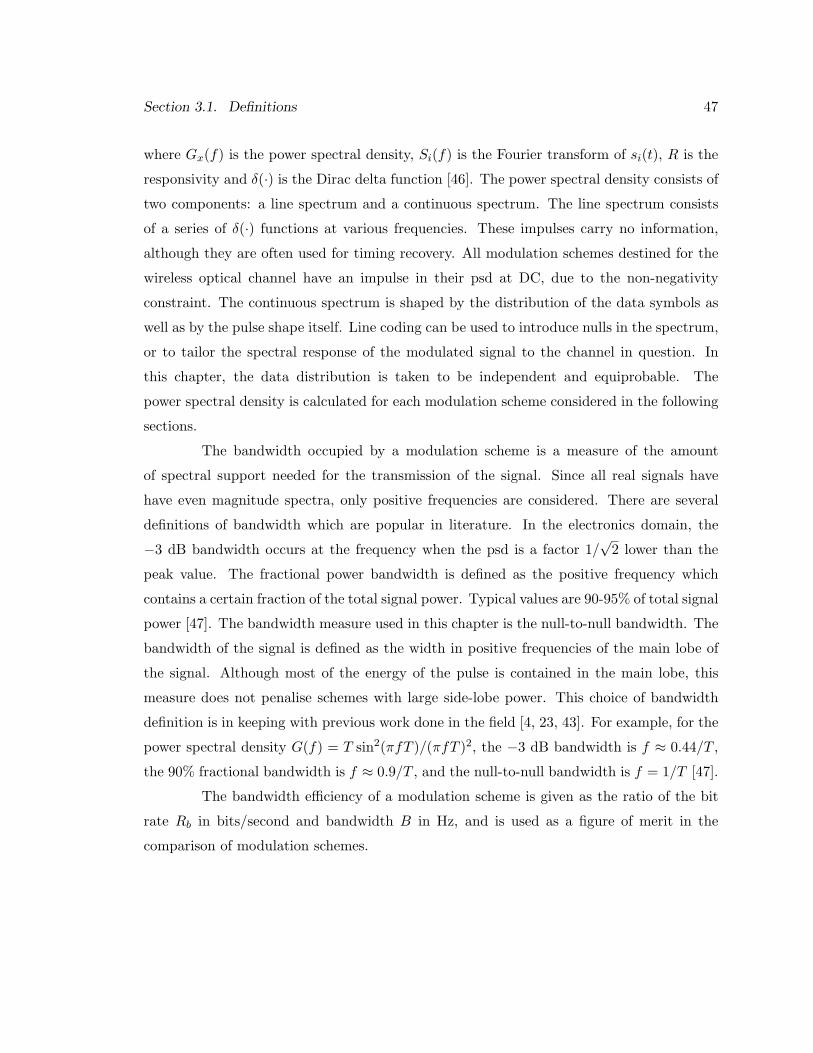
Section 3.1. Definitions 47
where Gx(f) is the power spectral density, Si(f) is the Fourier transform of si(t), R is the
responsivity and δ(·) is the Dirac delta function [46]. The power spectral density consists of
two components: a line spectrum and a continuous spectrum. The line spectrum consists
of a series of δ(·) functions at various frequencies. These impulses carry no information,
although they are often used for timing recovery. All modulation schemes destined for the
wireless optical channel have an impulse in their psd at DC, due to the non-negativity
constraint. The continuous spectrum is shaped by the distribution of the data symbols as
well as by the pulse shape itself. Line coding can be used to introduce nulls in the spectrum,
or to tailor the spectral response of the modulated signal to the channel in question. In
this chapter, the data distribution is taken to be independent and equiprobable. The
power spectral density is calculated for each modulation scheme considered in the following
sections.
The bandwidth occupied by a modulation scheme is a measure of the amount
of spectral support needed for the transmission of the signal. Since all real signals have
have even magnitude spectra, only positive frequencies are considered. There are several
definitions of bandwidth which are popular in literature. In the electronics domain, the
−3 dB bandwidth occurs at the frequency when the psd is a factor 1/√
2 lower than the
peak value. The fractional power bandwidth is defined as the positive frequency which
contains a certain fraction of the total signal power. Typical values are 90-95% of total signal
power [47]. The bandwidth measure used in this chapter is the null-to-null bandwidth. The
bandwidth of the signal is defined as the width in positive frequencies of the main lobe of
the signal. Although most of the energy of the pulse is contained in the main lobe, this
measure does not penalise schemes with large side-lobe power. This choice of bandwidth
definition is in keeping with previous work done in the field [4, 23, 43]. For example, for the
power spectral density G(f) = T sin2(πfT )/(πfT )2, the −3 dB bandwidth is f ≈ 0.44/T ,
the 90% fractional bandwidth is f ≈ 0.9/T , and the null-to-null bandwidth is f = 1/T [47].
The bandwidth efficiency of a modulation scheme is given as the ratio of the bit
rate Rb in bits/second and bandwidth B in Hz, and is used as a figure of merit in the
comparison of modulation schemes.
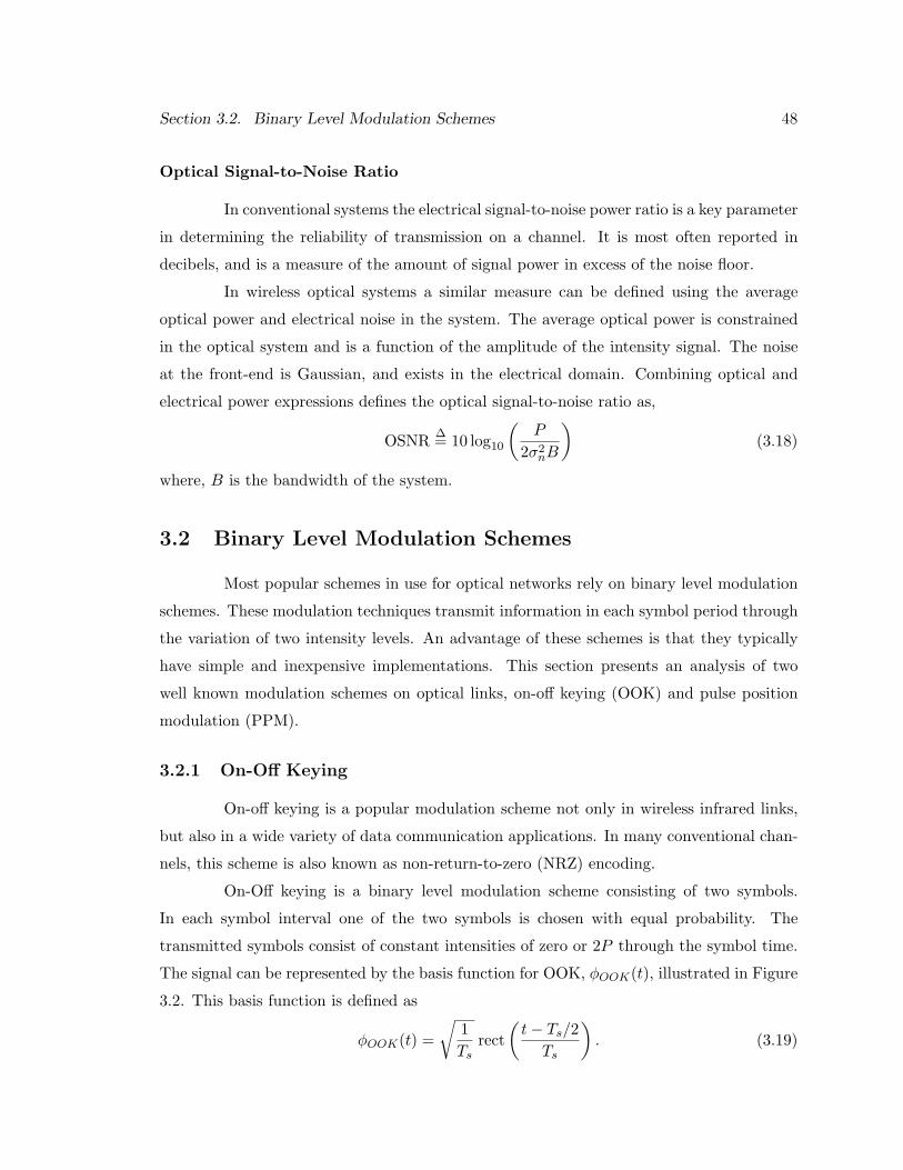
Section 3.2. Binary Level Modulation Schemes 48
Optical Signal-to-Noise Ratio
In conventional systems the electrical signal-to-noise power ratio is a key parameter
in determining the reliability of transmission on a channel. It is most often reported in
decibels, and is a measure of the amount of signal power in excess of the noise floor.
In wireless optical systems a similar measure can be defined using the average
optical power and electrical noise in the system. The average optical power is constrained
in the optical system and is a function of the amplitude of the intensity signal. The noise
at the front-end is Gaussian, and exists in the electrical domain. Combining optical and
electrical power expressions defines the optical signal-to-noise ratio as,
OSNR ∆= 10 log10
(P
2σ2nB
)(3.18)
where, B is the bandwidth of the system.
3.2 Binary Level Modulation Schemes
Most popular schemes in use for optical networks rely on binary level modulation
schemes. These modulation techniques transmit information in each symbol period through
the variation of two intensity levels. An advantage of these schemes is that they typically
have simple and inexpensive implementations. This section presents an analysis of two
well known modulation schemes on optical links, on-off keying (OOK) and pulse position
modulation (PPM).
3.2.1 On-Off Keying
On-off keying is a popular modulation scheme not only in wireless infrared links,
but also in a wide variety of data communication applications. In many conventional chan-
nels, this scheme is also known as non-return-to-zero (NRZ) encoding.
On-Off keying is a binary level modulation scheme consisting of two symbols.
In each symbol interval one of the two symbols is chosen with equal probability. The
transmitted symbols consist of constant intensities of zero or 2P through the symbol time.
The signal can be represented by the basis function for OOK, φOOK(t), illustrated in Figure
3.2. This basis function is defined as
φOOK(t) =√
1Ts
rect(
t− Ts/2Ts
). (3.19)

Section 3.2. Binary Level Modulation Schemes 49
2RP√
Ts0
φOOK
0 Ts
√1Ts
t
φOOK(t)
(a) (b)
Figure 3.2: Basis function (a) and constellation (b) of on-off keying.
Using this basis function, an expression for the time varying optical intensity is
x(t) =∞∑
k=−∞2P
√TsakφOOK(t− kTs) (3.20)
where ak ∈ 0, 1. Since the basis function is non-negative in the symbol period, and since
only non-negative multipliers are used, x(t) satisfies the non-negativity constraint. The
average amplitude of x(t) is set at P due to the distribution of the data symbols and the
scaling of the multipliers.
The constellation for OOK consists of two points in a one dimensional space as il-
lustrated in Figure 3.2. The probability of a bit error can be determined using the previously
defined framework as
Pe = Q
(RP√Rbσ2
n
)
since the bit rate Rb = 1/Ts and Pe(sym) = Pe in this case. The constellation figure of
merit can be calculated, following (3.14) as
CFMOOK =2R√Rb
.
The power spectral density of OOK was calculated to determine the bandwidth of
the system. Using (3.17), the power spectral density of OOK was found to be
GOOK(f) = (RP )2δ(f) + (RP )2Ts sinc2(πfTs),
where sinc(x) = sin(x)/x. Figure 3.3 contains a plot of the continuous portion of power
spectral density of OOK, indicating that the bandwidth, as defined earlier, is 1/Ts Hz.
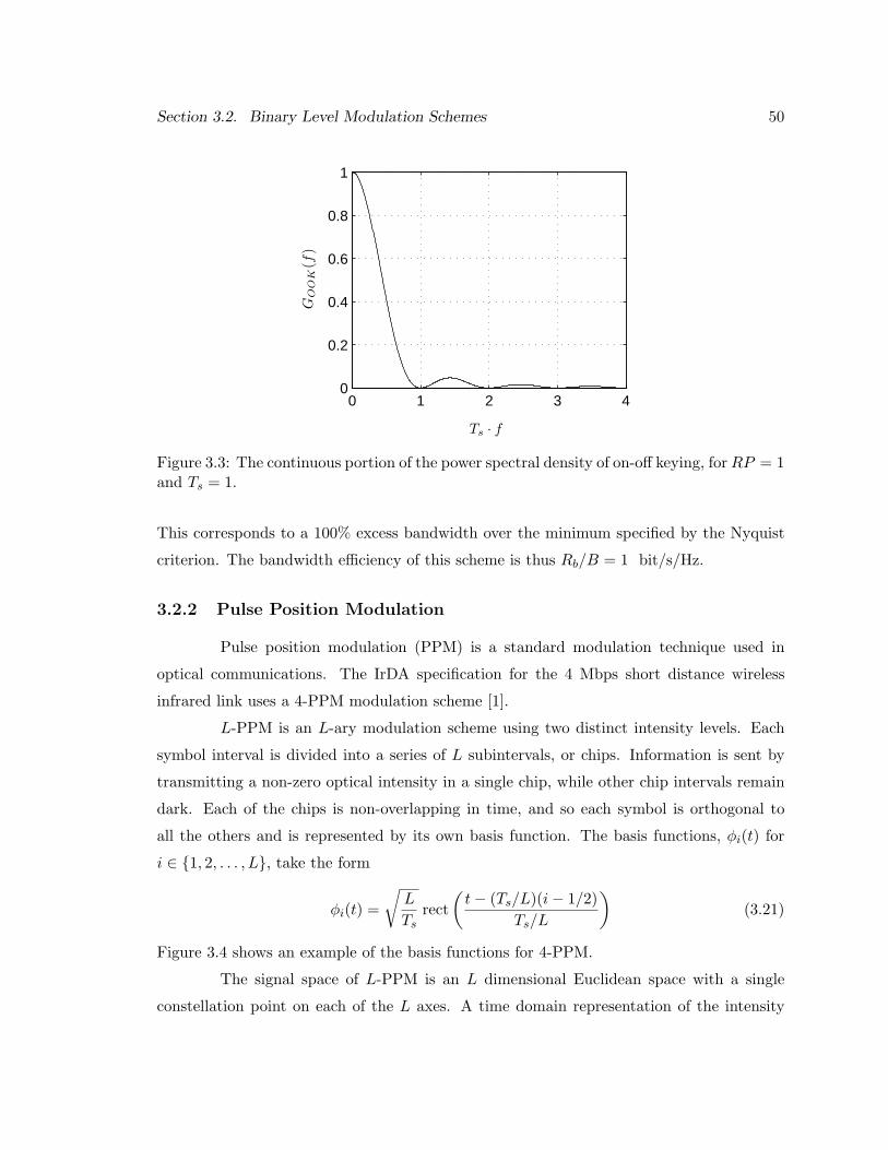
Section 3.2. Binary Level Modulation Schemes 50
0 1 2 3 40
0.2
0.4
0.6
0.8
1
GO
OK
(f)
Ts · f
Figure 3.3: The continuous portion of the power spectral density of on-off keying, for RP = 1and Ts = 1.
This corresponds to a 100% excess bandwidth over the minimum specified by the Nyquist
criterion. The bandwidth efficiency of this scheme is thus Rb/B = 1 bit/s/Hz.
3.2.2 Pulse Position Modulation
Pulse position modulation (PPM) is a standard modulation technique used in
optical communications. The IrDA specification for the 4 Mbps short distance wireless
infrared link uses a 4-PPM modulation scheme [1].
L-PPM is an L-ary modulation scheme using two distinct intensity levels. Each
symbol interval is divided into a series of L subintervals, or chips. Information is sent by
transmitting a non-zero optical intensity in a single chip, while other chip intervals remain
dark. Each of the chips is non-overlapping in time, and so each symbol is orthogonal to
all the others and is represented by its own basis function. The basis functions, φi(t) for
i ∈ 1, 2, . . . , L, take the form
φi(t) =√
L
Tsrect
(t− (Ts/L)(i− 1/2)
Ts/L
)(3.21)
Figure 3.4 shows an example of the basis functions for 4-PPM.
The signal space of L-PPM is an L dimensional Euclidean space with a single
constellation point on each of the L axes. A time domain representation of the intensity

Section 3.2. Binary Level Modulation Schemes 51
√4Ts
t
√4Ts
φ1(t)
t
√4Ts
φ4(t)
t
√4Ts
φ2(t)
t
φ3(t)
Ts0
Ts0 0
0 Ts
Ts
Figure 3.4: Basis functions for 4-PPM.
waveform as sent on the channel is
x(t) =∞∑
k=−∞LP
√Ts
Lφak
(t− kTs)
where ak chooses the basis function according to the symbol to be sent with ak ∈ 1, 2, . . . , L.The pulses remain non-negative for all time due to their construction. The average optical
power of each symbol is fixed at P by setting the peak value of each symbol to LP . The
information in this system is transmitted in the position of the pulse within the symbol
interval.
The probability of error for this modulation scheme can be calculated by noting
that each constellation point is orthogonal to all others and that each constellation point is
equidistant to all the other points. Based on this geometry the probability of symbol error
can be found as
Pe(sym) ≈ (L− 1) ·Q(
RP
√L
2Rsσ2n
).
Due to the orthogonality of all the points in the space, and the fact they are equiprobable,
the probability of symbol error can be converted to a probability of bit error by multiplying

Section 3.2. Binary Level Modulation Schemes 52
by a factor of L2 /(L− 1) [48]. Combining these results gives the probability of bit error as
Pe ≈ L
2·Q
(RP
√L log2 L
2Rbσ2n
)
since the bit rate Rb = Rs log2 L in this case. The CFM for PPM can be written directly
from the probability of symbol error expression as,
CFMPPM = R
√2L log2 L
Rb.
The characteristics of PPM are well suited to fibre applications. Fibre optical links
are limited by the thermal noise of the electronics, as noted in Chapter 2. However, insight
into the fundamental workings of optical transmission are gained by considering the optical
channel apart from the electronics. In this regime, the main impediment to communication
is due to the discrete nature of photons and electrons. The random arrival times of photons,
the random motion of electrons across the potential barrier include a random, yet signal
dependent noise source in the link. In these types of links, the receiver is modelled as an
electron counter over discrete intervals of time. If K is a random variable indicating the
number of electrons received in a given interval, the probability of receiving k electrons is
modelled as the Poisson distribution PrK = k = exp(−λ)λk/k!, where λ is the average
number of received electrons per interval.
Significant work has been done on the consideration of pulses transmitted on Pois-
son counting channels. Indeed, this scenario is merely a low intensity illumination case
of the Gaussian noise limited channel considered in this chapter. For modulation schemes
with only two symbols and in which the average output amplitude is limited, the optimum
signal set has been derived using a signal-to-noise ratio criterion similar to a matched filter
relationship. If the symbol period is broken into J counting intervals, each signal can be
represented as a vector of J electron counts. This optimum signal set is represented by the
count vectors
s0 = 0
s1 = v ∈ RJ | vj = S · δjo ,v = vj, j = 1, 2, . . . , J
where s0 and s1 represent the two symbol vectors, S is a scaling factor and δjo is 1 for some
jo ∈ 1, 2, . . . , J and zero otherwise [49, 50]. Appendix A contains a simple proof which
confirms this result using a distance criterion.

Section 3.2. Binary Level Modulation Schemes 53
This work has been extended to prove the optimality of L-ary modulation tech-
niques as well. It has been shown that the following intensity set of L waveforms is optimal
for average amplitude limited signalling on a Poisson counting channel :
si = v ∈ RL | vj = S · δij ,v = vj, j = 1, 2, . . . , L
for i = 1, 2, . . . , L where S is a scaling factor and δij is the Kronecker delta function [51].
Some have even gone so far as to conjecture that the above modulation scheme may be
optimal in a global sense for a Poisson counting receiver, although no proof was provided
[40].
Therefore, for channels in which the average output amplitude is limited, signifi-
cant theoretical work has been done to establish that concentrating symbol energy in disjoint
short intervals is beneficial. L-PPM approximates these “optimal” pulses to provide a large
separation in the signal space, and hence a lower Pe, for a given average optical power. The
high power efficiency of PPM can also be explained using the channel constraints along with
the signal space concepts, as demonstrated in Section 3.1.3. For a given P , PPM maximises
the vector coordinate values in (3.8) while keeping the average of the basis function low.
The average value of the basis functions is equal and set at√
Ts/L, which decreases with
increasing dimensionality. The magnitude of the coordinate factors increase as L. As a
result, for a given P , the distance between signal points increases with L to yield a lower
probability of error. PPM enjoys wide application in wireless and wired optical networks
due to its high power efficiency.
The price paid for this power efficiency is a reduction in the bandwidth efficiency of
the scheme. Qualitatively, the concentration of power in short pulses spreads the frequency
spectrum over a wide range. Using (3.17), the power spectral density of L-PPM is
GPPM (f) = (RP )2δ(f)
+(RP )2Ts sinc2
(πfTs
L
)[1− 1
L2
(L + 2
L−1∑
i=1
(L− i) cos(
2πfTs
Li
))].
Figure 3.5 contains an example of the continuous power spectral density for 4-PPM. This re-
sult can be generalised to show that the occupied bandwidth is B = L/Ts = LRs. Following
this expression, the bandwidth efficiency is given as
Rb
B=
1L
log2 Lbits/sHz
since Rs = Rb/ log2 L.
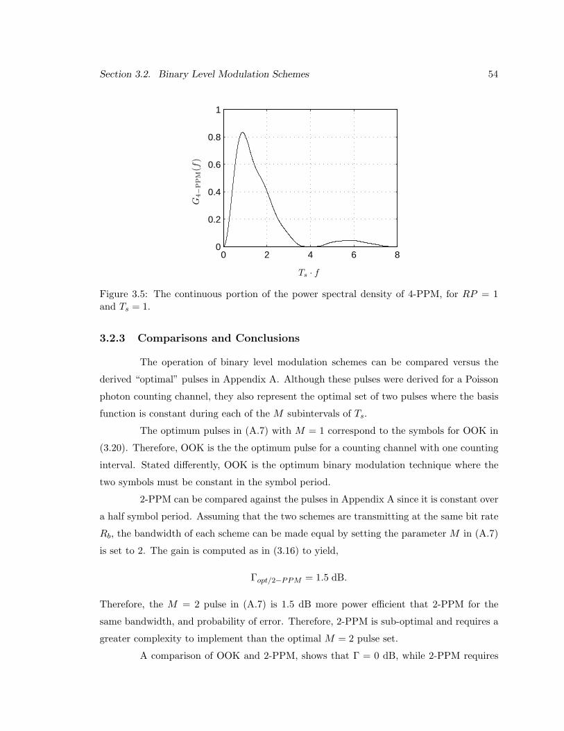
Section 3.2. Binary Level Modulation Schemes 54
0 2 4 6 80
0.2
0.4
0.6
0.8
1
Ts · f
G4−
PPM
(f)
Figure 3.5: The continuous portion of the power spectral density of 4-PPM, for RP = 1and Ts = 1.
3.2.3 Comparisons and Conclusions
The operation of binary level modulation schemes can be compared versus the
derived “optimal” pulses in Appendix A. Although these pulses were derived for a Poisson
photon counting channel, they also represent the optimal set of two pulses where the basis
function is constant during each of the M subintervals of Ts.
The optimum pulses in (A.7) with M = 1 correspond to the symbols for OOK in
(3.20). Therefore, OOK is the the optimum pulse for a counting channel with one counting
interval. Stated differently, OOK is the optimum binary modulation technique where the
two symbols must be constant in the symbol period.
2-PPM can be compared against the pulses in Appendix A since it is constant over
a half symbol period. Assuming that the two schemes are transmitting at the same bit rate
Rb, the bandwidth of each scheme can be made equal by setting the parameter M in (A.7)
is set to 2. The gain is computed as in (3.16) to yield,
Γopt/2−PPM = 1.5 dB.
Therefore, the M = 2 pulse in (A.7) is 1.5 dB more power efficient that 2-PPM for the
same bandwidth, and probability of error. Therefore, 2-PPM is sub-optimal and requires a
greater complexity to implement than the optimal M = 2 pulse set.
A comparison of OOK and 2-PPM, shows that Γ = 0 dB, while 2-PPM requires

Section 3.3. Multilevel Modulation Schemes 55
twice the bandwidth of OOK for the same Rb. Therefore, the advantage of using PPM
comes in using it with greater than two symbols.
Binary level modulation schemes provide an efficient means to implement mod-
ulation for optical links which are limited by the amount of transmitted power. In fibre
applications, which are primarily loss limited, these schemes are popular due to their high
average optical power efficiency.
The price paid for this advantage is that the bandwidth efficiency of the schemes is
poor. For fibre links, where the medium has thousands of gigahertz of unused bandwidth,
this is an acceptable trade-off. However, inexpensive, wireless optical links do not share
this luxury. In order to be able to attain high speed data transmission with current opto-
electronics, bandwidth efficiencies greater than 1 are required. This motivates the study of
multilevel modulation schemes for wireless optical channels.
3.3 Multilevel Modulation Schemes
Traditional approaches to modulation for the optical intensity channel centre on
developing power efficient schemes. The bandwidth of the transmitted symbols is not a
critical issue due to the wide bandwidth available in fibre systems. However, the wireless
optical channel relies on the use of inexpensive devices which are severely limited in available
bandwidth, as shown in Chapter 2. As a result, for wireless optical links, the bandwidth
efficiency of the modulation scheme is a parameter of critical importance.
Multilevel modulation techniques transmit symbols in which the intensity values
are continuous in a range or take on a set of values. The advantage of these schemes is
that they provide a higher bandwidth efficiency than binary level techniques, since data is
transmitted in the amplitude level as well as the structure of the basis functions.
This section presents an analysis of two classical multilevel schemes for the intensity
modulated channel: pulse amplitude modulation (PAM) and quadrature pulse amplitude
modulation (QAM).
3.3.1 Pulse Amplitude Modulation
Pulse amplitude modulation is a classical modulation scheme which can be adapted
to operate on an intensity modulated optical channel. PAM is a generalisation of on-off
keying from a set of two symbols to a set of L symbols. The basis function for L-PAM is
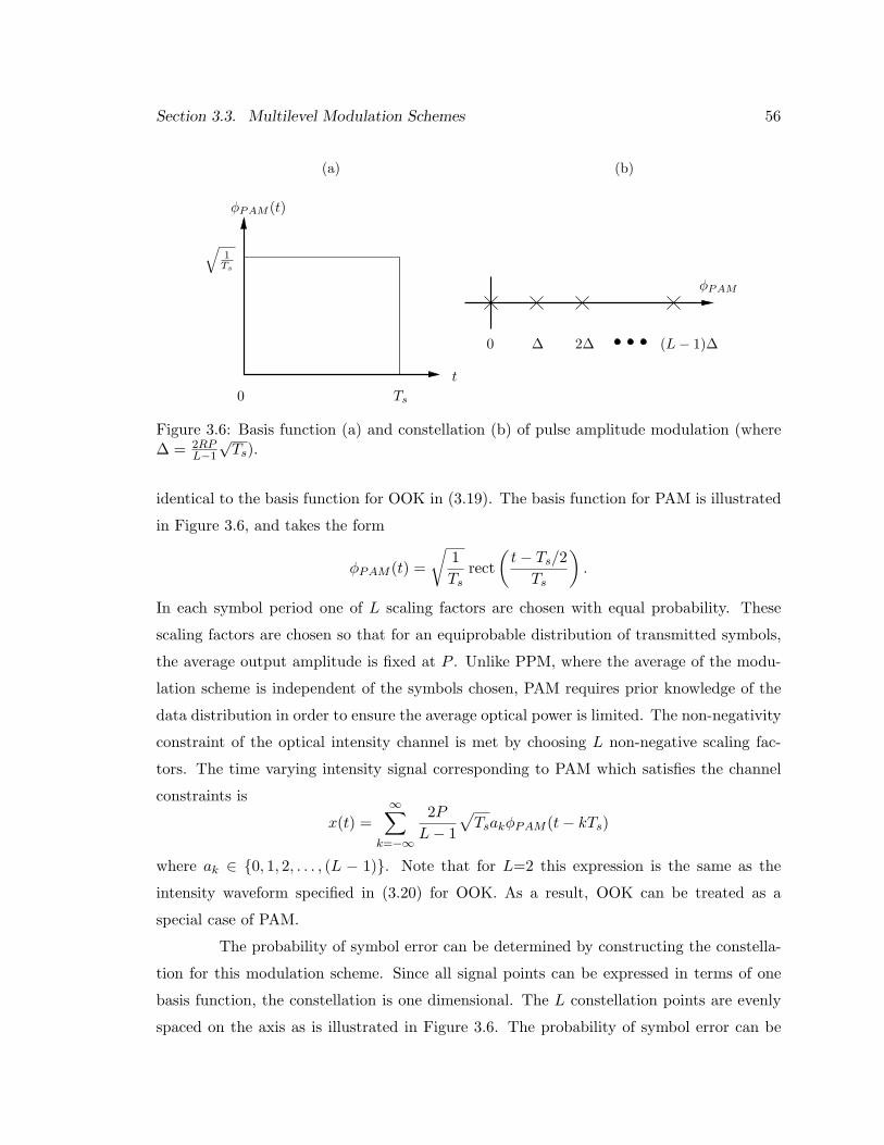
Section 3.3. Multilevel Modulation Schemes 56
0 Ts
√1Ts
t
φPAM (t)
(a) (b)
0 ∆ 2∆ (L− 1)∆
φPAM
Figure 3.6: Basis function (a) and constellation (b) of pulse amplitude modulation (where∆ = 2RP
L−1
√Ts).
identical to the basis function for OOK in (3.19). The basis function for PAM is illustrated
in Figure 3.6, and takes the form
φPAM (t) =√
1Ts
rect(
t− Ts/2Ts
).
In each symbol period one of L scaling factors are chosen with equal probability. These
scaling factors are chosen so that for an equiprobable distribution of transmitted symbols,
the average output amplitude is fixed at P . Unlike PPM, where the average of the modu-
lation scheme is independent of the symbols chosen, PAM requires prior knowledge of the
data distribution in order to ensure the average optical power is limited. The non-negativity
constraint of the optical intensity channel is met by choosing L non-negative scaling fac-
tors. The time varying intensity signal corresponding to PAM which satisfies the channel
constraints is
x(t) =∞∑
k=−∞
2P
L− 1
√TsakφPAM (t− kTs)
where ak ∈ 0, 1, 2, . . . , (L − 1). Note that for L=2 this expression is the same as the
intensity waveform specified in (3.20) for OOK. As a result, OOK can be treated as a
special case of PAM.
The probability of symbol error can be determined by constructing the constella-
tion for this modulation scheme. Since all signal points can be expressed in terms of one
basis function, the constellation is one dimensional. The L constellation points are evenly
spaced on the axis as is illustrated in Figure 3.6. The probability of symbol error can be
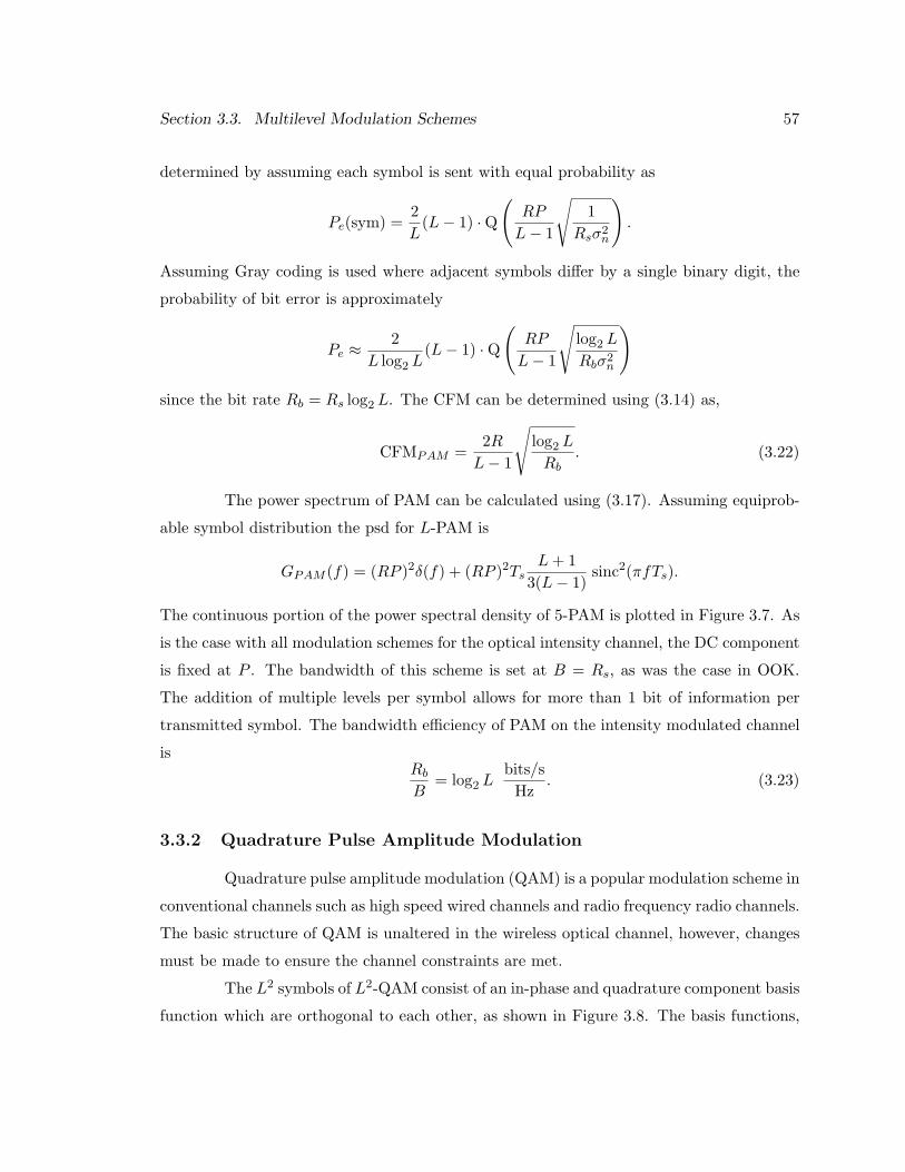
Section 3.3. Multilevel Modulation Schemes 57
determined by assuming each symbol is sent with equal probability as
Pe(sym) =2L
(L− 1) ·Q(
RP
L− 1
√1
Rsσ2n
).
Assuming Gray coding is used where adjacent symbols differ by a single binary digit, the
probability of bit error is approximately
Pe ≈ 2L log2 L
(L− 1) ·Q(
RP
L− 1
√log2 L
Rbσ2n
)
since the bit rate Rb = Rs log2 L. The CFM can be determined using (3.14) as,
CFMPAM =2R
L− 1
√log2 L
Rb. (3.22)
The power spectrum of PAM can be calculated using (3.17). Assuming equiprob-
able symbol distribution the psd for L-PAM is
GPAM (f) = (RP )2δ(f) + (RP )2TsL + 1
3(L− 1)sinc2(πfTs).
The continuous portion of the power spectral density of 5-PAM is plotted in Figure 3.7. As
is the case with all modulation schemes for the optical intensity channel, the DC component
is fixed at P . The bandwidth of this scheme is set at B = Rs, as was the case in OOK.
The addition of multiple levels per symbol allows for more than 1 bit of information per
transmitted symbol. The bandwidth efficiency of PAM on the intensity modulated channel
isRb
B= log2 L
bits/sHz
. (3.23)
3.3.2 Quadrature Pulse Amplitude Modulation
Quadrature pulse amplitude modulation (QAM) is a popular modulation scheme in
conventional channels such as high speed wired channels and radio frequency radio channels.
The basic structure of QAM is unaltered in the wireless optical channel, however, changes
must be made to ensure the channel constraints are met.
The L2 symbols of L2-QAM consist of an in-phase and quadrature component basis
function which are orthogonal to each other, as shown in Figure 3.8. The basis functions,

Section 3.3. Multilevel Modulation Schemes 58
0 1 2 3 40
0.1
0.2
0.3
0.4
0.5
G5−
PA
M(f
)
Ts · f
Figure 3.7: The continuous portion of the power spectral density of 5-PAM, for RP = 1and Ts = 1.
φI(t) and φQ(t), represent the in-phase and quadrature components of the data signal and
take the form
φI(t) =√
2Ts
cos (ωpt) rect(
t− Ts/2Ts
)
φQ(t) =√
2Ts
sin (ωpt) rect(
t− Ts/2Ts
)(3.24)
where ωk = 2pπ/Ts for any p ∈ N. In each symbol instant, independent data is used
to modulate the two basis functions. As a result, each basis function is multiplied by a
series of L amplitude values to comprise the L2 symbols. Taking into account the channel
constraints, the time varying intensity function, x(t) can be written as
x(t) =∞∑
k=−∞
P
2(L− 1)
√Ts (akφI(t− kTs) + bkφQ(t− kTs)) + P · rect
(t− Ts(k + 1/2)
Ts
).
(3.25)
for ak, bk ∈ −(L − 1),−(L − 3),−(L − 5), . . . , (L − 1). Since the basis functions φI(t)
and φQ(t) take on negative amplitudes at intervals within the symbol period, a DC bias
must be added to ensure the non-negativity constraint is met. QAM adds a fixed bias of P
to every symbol. This added DC bias is rejected by the matched filter front end since the
basis functions have an average value of zero. The addition of a fixed DC bias also ensures
that the average power constraint in (3.2) is met, independent of the data distribution. The
maximum amplitude value for the data is fixed at P√
Ts/2, and the minimum amplitude
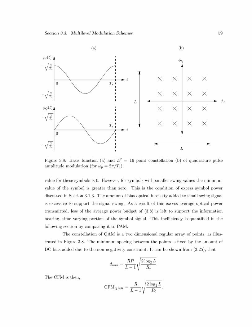
Section 3.3. Multilevel Modulation Schemes 59
φI(t)
t
φQ(t)
t
0
0 Ts
Ts
+√
2Ts
−√
2Ts
−√
2Ts
+√
2Ts
φQ
φI
L
L
(a) (b)
Figure 3.8: Basis function (a) and L2 = 16 point constellation (b) of quadrature pulseamplitude modulation (for ωp = 2π/Ts).
value for these symbols is 0. However, for symbols with smaller swing values the minimum
value of the symbol is greater than zero. This is the condition of excess symbol power
discussed in Section 3.1.3. The amount of bias optical intensity added to small swing signal
is excessive to support the signal swing. As a result of this excess average optical power
transmitted, less of the average power budget of (3.8) is left to support the information
bearing, time varying portion of the symbol signal. This inefficiency is quantified in the
following section by comparing it to PAM.
The constellation of QAM is a two dimensional regular array of points, as illus-
trated in Figure 3.8. The minimum spacing between the points is fixed by the amount of
DC bias added due to the non-negativity constraint. It can be shown from (3.25), that
dmin =RP
L− 1
√2 log2 L
Rb.
The CFM is then,
CFMQAM =R
L− 1
√2 log2 L
Rb.

Section 3.3. Multilevel Modulation Schemes 60
The probability of symbol error can be determined by applying the union bound approx-
imation in (3.13). By computing the average number of neighbours dmin away from each
constellation point, an estimate for Pe(sym) can be formed as
Pe(sym) ≈ 4(L− 1)L
·Q(
RP
L− 1
√1
4Rsσ2n
).
Using the Gray coding approximation, the probability of bit error for L2-QAM is found to
be
Pe ≈ 2(L− 1)L log2 L
·Q(
RP
L− 1
√log2 L
2Rbσ2n
)
where Rb = Rs log2 L2.
The spectral characteristics of QAM can be investigated by computing the power
spectral density via (3.17). The power spectral density for the L2-QAM signal in (3.25) is
GQAM (f) = (RP )2δ(f)
+(RP )2TsL + 1
12(L− 1)
[sinc2
(πTs
(f − 1
Ts
))+ sinc2
(πTs
(f +
1Ts
))].
Figure 3.9 illustrates an example of the continuous portion of the psd for 25-QAM. QAM
is a passband modulation scheme with little signal energy at low frequencies. This is
a beneficial trait in channels which are corrupted by low frequency interferers, such as
fluorescent lighting ballasts in wireless optical channels (see Section 2.4).
The bandwidth of L2-QAM, as defined by the frequency of the first spectral null,
is B = 2Rs Hz. Following this result, the bandwidth efficiency of L2-QAM is
Rb
B= log2 L
bits/sHz
.
which is identical to the bandwidth efficiency of L-PAM in (3.23). Although the bandwidth
required for L2-QAM is double that of L-PAM, the entropy of the QAM symbols is double
that of PAM, which satisfies intuition.
3.3.3 Comparisons and Conclusions
For the same bandwidth, bit rate and Pe(sym), ΓL−PAM/L2−QAM = 1.5 dB. This
is in contrast to a conventional channel, in which L-PAM and L2-QAM have the same
energy efficiency. The loss in power efficiency in the optical QAM constellation is due to
the fact that the fixed DC bias added to every symbol is excessive for the signals with small

Section 3.3. Multilevel Modulation Schemes 61
0 1 2 3 40
0.1
0.2
0.3
0.4
0.5
G25−
QA
M(f
)
Ts · f
Figure 3.9: The continuous portion of the power spectral density of 25-QAM, for RP = 1and Ts = 1.
amplitude. The excessive DC content of low amplitude symbols transmits no information
and reduces the power efficiency of the scheme as shown in Section 3.1.3.
The loss of average power efficiency in QAM over PAM can also be explained by
viewing QAM as a series of two orthogonal PAM signals. Since the average power is fixed
at P by the DC bias, the peak amplitude of the resulting modulated signal is P . According
to this constraint, the maximum value that any signal in either in-phase or quadrature
directions can take is P/√
2. 2 Therefore, each phase of L2-QAM behaves as an L-PAM
signal with its signal points distributed evenly between −P/√
2 and P/√
2. It is easy to
show that in this case, the distance between constellation points in this L-PAM signal is a
factor of√
2 smaller than in the L-PAM constellation in Section 3.3.1. Therefore, L2-QAM
constellation is 10 log10
√2 = 1.5 dB less power efficient than L-PAM for the same Pe and
bandwidth efficiency.
The comparison between L-PAM and L-PPM is necessary to justify the use of a
multilevel scheme over a binary system. Computing the gain of the two schemes assuming
the same Rb in both cases yields
ΓPPM/PAM = 5 log10
(L(L− 1)2
)− 1.5 dB,
2Note that the use of sinusoids as basis functions improves the power efficiency of QAM, since the peakvalue of the sum of sinusoids is the geometric sum of the component amplitudes, and not the linear sum.Therefore, the maximum of the sum of phases adds according to Pythagorean identity,
pa2
k + b2k, as in
(3.25), which fixes the maximum value per dimension at P/√
2 for a DC bias of P .

Section 3.4. Adaptively Biased QAM 62
which is greater than or equal to zero for all L ≥ 2. As the number of symbols increases
in either constellation it is clear that L-PPM enjoys a significant advantage over L-PAM
in the area of average power efficiency. For example, for 4-ary signalling 4-PPM has a
10 log10 4.24 = 6.3 dB average optical power advantage over 4-PAM.
However, since the wireless optical channel is constrained by bandwidth consid-
erations, the bandwidth of the two schemes must be compared as well. For the same Rb,
L-PPM requires L times more bandwidth than L-PAM. So, in the example of 4-ary sig-
nalling, although 4-PPM enjoys an average optical power advantage over 4-PAM, it requires
four times the bandwidth.
Multilevel schemes achieve the goal of increased bandwidth efficiency at the price
of reduced average optical power efficiency when compared to binary level schemes. Since
bandwidth restrictions on the wireless optical channel are a severe limitation for high speed
communications, highly bandwidth efficient schemes are required. At the same time, in
order to have a highly robust link, a high average power efficiency is needed. A modu-
lation scheme which conserves the bandwidth efficiency of L-PAM while improving on its
bandwidth efficiency is necessary for the high speed short distance infrared link.
3.4 Adaptively Biased QAM
In this section we present a new modulation scheme for the wireless infrared chan-
nel called Adaptively Biased QAM (AB-QAM). It improves the average optical power ef-
ficiency of current bandwidth efficient techniques while maintaining the same bandwidth
efficiency for a small increase in complexity [52].
This section introduces the basic structure of AB-QAM and shows that it meets all
the constraints imposed by the optical channel. The methodology used in the development of
AB-QAM is highlighted by examining a single phase of the modulation scheme. The spectral
characteristics of the modulation scheme are described via the power spectral density to
demonstrate the bandwidth efficiency of this scheme. The impact of fluorescent interferers
as well as the use of different pulse shapes is also briefly discussed. The section concludes
with comparison of AB-QAM to the multilevel techniques described earlier.

Section 3.4. Adaptively Biased QAM 63
3.4.1 Modulation Scheme Definition
The operation of AB-QAM is best described by using the signal space framework
of Section 3.1.2. The basis functions follow the methodology laid out in Section 3.1.3, where
one basis function defines the symbol average and the others vary in the symbol period.
The basis functions of AB-QAM are illustrated in Figure 3.10, and can also be represented
mathematically as
φ1(t) =√
1Ts
(rect
(t− Ts/2
Ts
)− 2 rect
(t− Ts/2
Ts/2
))
φ2(t) =√
1Ts
(rect
(t− Ts/2
Ts
)− 2 rect
(t− 3Ts/4
Ts/2
))
φ3(t) =√
1Ts
rect(
t− Ts/2Ts
). (3.26)
The basis function φ3(t) determines the average of each symbol, while φ1(t) and φ2(t) have
zero average value in the symbol period. 3
The collection of scaled basis functions forms all of the signals of the modulation
scheme. AB-QAM transmits one of L2 symbols per Ts, chosen independently and with
equal probability. The transmitted intensity waveform for L2-AB-QAM is denoted x(t) and
takes the form,
x(t) =∞∑
k=−∞
AP
(L− 1)
√Ts (akφ1(t− kTs) + bkφ2(t− kTs) + ckφ3(t− kTs)) (3.27)
for ak, bk ∈ −(L− 1),−(L− 3),−(L− 5), . . . , (L− 1), ck = |ak|+ |bk|, and
A =
LL+1 : for L2 odd;L−1
L : for L2 even.(3.28)
The information in this modulation scheme is carried in the independent choice of L values
for each ak and bk. The information sent on the φ3 basis is not independent, but is used to
satisfy the non-negativity constraint of the channel. The magnitude of the DC bias added
to the intensity waveform is equal to the sum of the amplitudes of the signals sent in the
φ1 and φ2 dimensions. This adaptive bias term added to each symbol is analogous to the
general case in (3.10), since the minimum amount of DC bias is added to each intensity
symbol to satisfy the non-negativity constraint.3If the signals in (3.26) are written in terms of the 4-ary basis functions in (3.21), the co-ordinates form
three rows of the 4 × 4 Hadamard matrix. The fourth row of the matrix, which is orthogonal to the otherthree, is not used since it requires twice the bandwidth.

Section 3.4. Adaptively Biased QAM 64
φ1
t
√1Ts
−√
1Ts
Ts
0
φ2
t
√1Ts
−√
1Ts
Ts
0
0 Ts
√1Ts
φ3
t
Figure 3.10: Basis functions for AB-QAM.
The average power of the modulation scheme is dependent on the data distribution.
The scaling term A is set to ensure that for equiprobable symbol selection the average power
is set at P . The need for different expressions for A in the case of odd and even sized
constellations is due to the fact that the constellation points are evenly spaced in the φ1
and φ2 directions. For even sized constellations, there is no zero symbol for either ak or bk,
which is reflected by the change in the scaling factor to maintain the same average optical
transmitted power. The derivation of these terms is given in more detail in the following
section.
3.4.2 Development
The motivation for the development of AB-QAM is to improve the optical power
efficiency of multilevel modulation schemes while conserving their bandwidth efficiency.
This section presents the central factors which improve the power efficiency of AB-QAM
over traditional multilevel schemes. The structure of the modulation scheme is justified by
considering a simple example, and then generalising it to the AB-QAM case.
Section 3.4. Adaptively Biased QAM 65
Adaptively Biased PAM
The key ideas which lead to the power efficiency of AB-QAM can be analysed using
a single phase of the modulation scheme. Suppose a modulation scheme, named adaptively
biased PAM (AB-PAM), is defined using basis functions φ2(t) and φ3(t) in (3.26) and Figure
3.10. The optical intensity waveform for this modulation scheme is
x(t) =∞∑
k=−∞
AP
(L− 1)
√Ts (bkφ2(t− kTs) + ckφ3(t− kTs))
for bk ∈ −(L−1),−(L−3),−(L−5), . . . , (L−1), ck = |bk|, and A is a scaling factor used
to ensure that the average optical power constraint is met. The fundamental idea of AB-
PAM is the same as that for AB-QAM : in each symbol instant, a scaled time varying pulse
is sent, and the minimum amount of DC bias is added to ensure that the non-negativity
constraint in (3.10) is met. It was also shown in (3.12) that this intuitive notion of sending
zero excess average optical power for improved power efficiency was justified.
The scaling factor A determines the average power of AB-PAM. The scaling factors
for φ2(t) are evenly spaced from −(L−1) to (L−1) to ensure the same dmin between adjacent
symbols. Due to this fact, schemes with an odd number of signal points will have a zero
symbol, while constellations with an even number of points will not have a zero symbol. Due
to this asymmetry, the value of A for the AB-PAM modulation scheme with L constellation
points can be found to be,
A =
2LL+1 : for L odd;
2(L−1)L : for L even.
(3.29)
If the symbols are detected using a filter matched to φ2(t) only, then the minimum
distance between the constellation points is a function of the scaling factor A and the
number of points L for a fixed P , and Rb. The CFM for AB-PAM can be written as,
CFMAB−PAM =2RA
L− 1
√log2 L
Rb. (3.30)
The gain of AB-PAM over PAM using the information from the φ2 dimension only, Γ(1)AB−P ,
can be determined using the CFM of PAM in (3.22) and (3.30) as,
Γ(1)AB−P =
3 + 10 log10
(L
L+1
)dB : for L odd
3 + 10 log10
(L−1
L
)dB : for L even
(3.31)
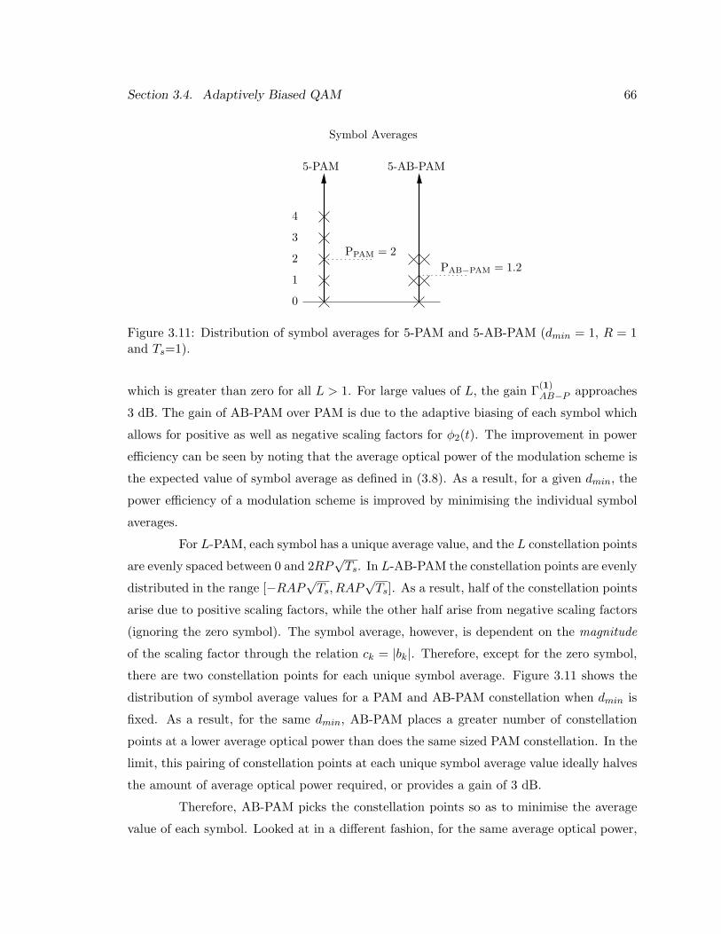
Section 3.4. Adaptively Biased QAM 66
Symbol Averages
5-PAM 5-AB-PAM
0
1
3
4
2PAB−PAM = 1.2
PPAM = 2
Figure 3.11: Distribution of symbol averages for 5-PAM and 5-AB-PAM (dmin = 1, R = 1and Ts=1).
which is greater than zero for all L > 1. For large values of L, the gain Γ(1)AB−P approaches
3 dB. The gain of AB-PAM over PAM is due to the adaptive biasing of each symbol which
allows for positive as well as negative scaling factors for φ2(t). The improvement in power
efficiency can be seen by noting that the average optical power of the modulation scheme is
the expected value of symbol average as defined in (3.8). As a result, for a given dmin, the
power efficiency of a modulation scheme is improved by minimising the individual symbol
averages.
For L-PAM, each symbol has a unique average value, and the L constellation points
are evenly spaced between 0 and 2RP√
Ts. In L-AB-PAM the constellation points are evenly
distributed in the range [−RAP√
Ts, RAP√
Ts]. As a result, half of the constellation points
arise due to positive scaling factors, while the other half arise from negative scaling factors
(ignoring the zero symbol). The symbol average, however, is dependent on the magnitude
of the scaling factor through the relation ck = |bk|. Therefore, except for the zero symbol,
there are two constellation points for each unique symbol average. Figure 3.11 shows the
distribution of symbol average values for a PAM and AB-PAM constellation when dmin is
fixed. As a result, for the same dmin, AB-PAM places a greater number of constellation
points at a lower average optical power than does the same sized PAM constellation. In the
limit, this pairing of constellation points at each unique symbol average value ideally halves
the amount of average optical power required, or provides a gain of 3 dB.
Therefore, AB-PAM picks the constellation points so as to minimise the average
value of each symbol. Looked at in a different fashion, for the same average optical power,
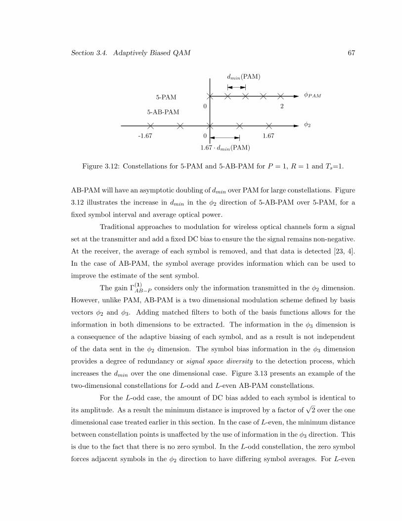
Section 3.4. Adaptively Biased QAM 67
φPAM
φ2
0-1.67 1.67
0 2
dmin(PAM)
1.67 · dmin(PAM)
5-PAM
5-AB-PAM
Figure 3.12: Constellations for 5-PAM and 5-AB-PAM for P = 1, R = 1 and Ts=1.
AB-PAM will have an asymptotic doubling of dmin over PAM for large constellations. Figure
3.12 illustrates the increase in dmin in the φ2 direction of 5-AB-PAM over 5-PAM, for a
fixed symbol interval and average optical power.
Traditional approaches to modulation for wireless optical channels form a signal
set at the transmitter and add a fixed DC bias to ensure the the signal remains non-negative.
At the receiver, the average of each symbol is removed, and that data is detected [23, 4].
In the case of AB-PAM, the symbol average provides information which can be used to
improve the estimate of the sent symbol.
The gain Γ(1)AB−P considers only the information transmitted in the φ2 dimension.
However, unlike PAM, AB-PAM is a two dimensional modulation scheme defined by basis
vectors φ2 and φ3. Adding matched filters to both of the basis functions allows for the
information in both dimensions to be extracted. The information in the φ3 dimension is
a consequence of the adaptive biasing of each symbol, and as a result is not independent
of the data sent in the φ2 dimension. The symbol bias information in the φ3 dimension
provides a degree of redundancy or signal space diversity to the detection process, which
increases the dmin over the one dimensional case. Figure 3.13 presents an example of the
two-dimensional constellations for L-odd and L-even AB-PAM constellations.
For the L-odd case, the amount of DC bias added to each symbol is identical to
its amplitude. As a result the minimum distance is improved by a factor of√
2 over the one
dimensional case treated earlier in this section. In the case of L-even, the minimum distance
between constellation points is unaffected by the use of information in the φ3 direction. This
is due to the fact that there is no zero symbol. In the L-odd constellation, the zero symbol
forces adjacent symbols in the φ2 direction to have differing symbol averages. For L-even

Section 3.4. Adaptively Biased QAM 68
0
φ3
φ2
dmin = ∆
0
∆
∆
φ3
φ2
dmin =√
2∆
6-AB-PAM
5-AB-PAM
∆
∆
Figure 3.13: Constellations of 5-AB-PAM and 6-AB-PAM in the φ2 and φ3 dimensions. Notethe bold lines indicate the dmin of the constellation, and ∆ indicates the one-dimensionalminimum distance.

Section 3.4. Adaptively Biased QAM 69
the absence of this zero symbol causes the minimum distance for the pair of points with
lowest symbol average to be unchanged from the one dimensional case.
The gain of AB-PAM over PAM using the information contained in the two dimen-
sions is denoted Γ(2)AB−P . Using the definition of Γ(1)
AB−P in (3.31), the gain can be written
as
Γ(2)AB−P =
Γ(1)AB−P + 1.5 dB : for L odd;
Γ(1)AB−P : for L even.
(3.32)
From AB-PAM to AB-QAM
Although AB-PAM offers a significant improvement in power efficiency over PAM,
it suffers from a reduction in the bandwidth efficiency. It can be shown that the bandwidth
efficiency of AB-PAM is half of that for PAM. Since bandwidth efficiency is a key param-
eter for inexpensive wireless optical links, steps must be taken to preserve the bandwidth
efficiency of PAM and maintain some of the power efficiency improvement of AB-PAM.
In order to recoup the bandwidth efficiency of AB-PAM another data bearing
signal is added in quadrature to φ2. The basis function φ1(t) in (3.26) is orthogonal to
φ2(t) and φ3(t), and has the same bandwidth requirements as φ2(t). As a result, AB-QAM
is formed by composing two information bearing signals in quadrature, and then adding
sufficient DC bias to ensure the non-negativity constraint is met. This preserves the basic
AB-PAM framework while providing the same bandwidth efficiency as PAM.
The cost associated with this method is that the amplitude values allowed for
each phase are halved from those allowed in AB-PAM. This is because the amplitudes of
the φ1 and φ2 phases are linearly related to the DC bias which must be added to ensure
non-negativity. Since the two phases send independent data, it is as if two AB-PAM signals
were combined to form the AB-QAM signal. This addition of the signals, causes the average
of each phase to add as well. As a result, the 3 dB improvement Γ(1)AB−P of AB-PAM, is lost
in AB-QAM.
3.4.3 Probability of Error Analysis
In order to determine the error performance of AB-QAM, the geometry of the
signal space must be investigated. AB-QAM is a three dimensional modulation scheme
defined by φ1, φ2 and φ3 in (3.26). The information contained in all three dimensions is
used to form the estimate of the received symbol.

Section 3.4. Adaptively Biased QAM 70
One of the basic principles behind AB-QAM is that the DC bias added per symbol
is equal to the sum of the magnitudes of the data sent in the φ1 and φ2 directions. Ignoring
the scaling factors, if x and y are taken to represent the amplitudes of the the data symbols
in the φ2 and φ2 directions respectively, the amount of DC bias added to each symbol is
z = |x|+ |y|. (3.33)
This expression defines a set of four intersecting planes in R3 defined by the various per-
mutations of sign for x and y and where z ≥ 0. Due to the construction of the modulation
scheme, all the constellation points of AB-QAM lie on the surface defined in (3.33). Suppose
that only one of the bounding planes is considered, z = x + y, where z, x, y ≥ 0. It can be
shown that all the AB-QAM constellation points in this bounding plane can be written in
terms of the [x, y, z]T basis vectors,
ν1 =
1
0
1
, ν2 =
0
1
1
.
This definition of basis vectors satisfies intuition since every change in the magnitude of the
x or y signal values is accompanied by the same change in DC bias added through the z
coordinate. The set of constellation points in the bounding plane in question form a subset
of points of the infinite lattice defined by ν1 and ν2. The packing density of the lattice
can be found to equal π/√
12, which is the most dense packing possible in two dimensions.
This lattice is termed hexagonal, since each constellation point has six neighbours and the
distance between any two points is the same throughout the lattice [53]. Generalising, the
constellation points in each of the bounding planes of AB-QAM are subsets of the hexagonal
lattice in two dimensions. Since the minimum distance between all points in each plane is
the same, dmin of the modulation scheme is determined by either the spacing of the lattice
points or due to distances between points in adjacent planes at the interface of the four
bounding planes.
Figure 3.14 shows the constellation for two AB-QAM schemes. The distance be-
tween points in the φ1-φ2 plane is set at ∆ = 1. In order to aid in the visualisation of the
constellation, the constellation is drawn from two orthogonal views. Due to the symmetry
of the constellations, these two views capture the positioning of points in the space. The
dotted lines indicate contours which represent a unique bias level in the φ3 dimension that
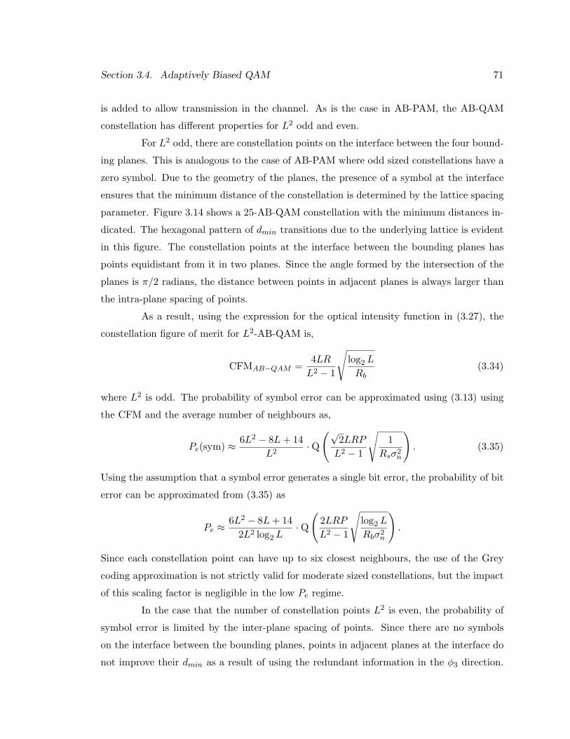
Section 3.4. Adaptively Biased QAM 71
is added to allow transmission in the channel. As is the case in AB-PAM, the AB-QAM
constellation has different properties for L2 odd and even.
For L2 odd, there are constellation points on the interface between the four bound-
ing planes. This is analogous to the case of AB-PAM where odd sized constellations have a
zero symbol. Due to the geometry of the planes, the presence of a symbol at the interface
ensures that the minimum distance of the constellation is determined by the lattice spacing
parameter. Figure 3.14 shows a 25-AB-QAM constellation with the minimum distances in-
dicated. The hexagonal pattern of dmin transitions due to the underlying lattice is evident
in this figure. The constellation points at the interface between the bounding planes has
points equidistant from it in two planes. Since the angle formed by the intersection of the
planes is π/2 radians, the distance between points in adjacent planes is always larger than
the intra-plane spacing of points.
As a result, using the expression for the optical intensity function in (3.27), the
constellation figure of merit for L2-AB-QAM is,
CFMAB−QAM =4LR
L2 − 1
√log2 L
Rb(3.34)
where L2 is odd. The probability of symbol error can be approximated using (3.13) using
the CFM and the average number of neighbours as,
Pe(sym) ≈ 6L2 − 8L + 14L2
·Q(√
2LRP
L2 − 1
√1
Rsσ2n
). (3.35)
Using the assumption that a symbol error generates a single bit error, the probability of bit
error can be approximated from (3.35) as
Pe ≈ 6L2 − 8L + 142L2 log2 L
·Q(
2LRP
L2 − 1
√log2 L
Rbσ2n
).
Since each constellation point can have up to six closest neighbours, the use of the Grey
coding approximation is not strictly valid for moderate sized constellations, but the impact
of this scaling factor is negligible in the low Pe regime.
In the case that the number of constellation points L2 is even, the probability of
symbol error is limited by the inter-plane spacing of points. Since there are no symbols
on the interface between the bounding planes, points in adjacent planes at the interface do
not improve their dmin as a result of using the redundant information in the φ3 direction.
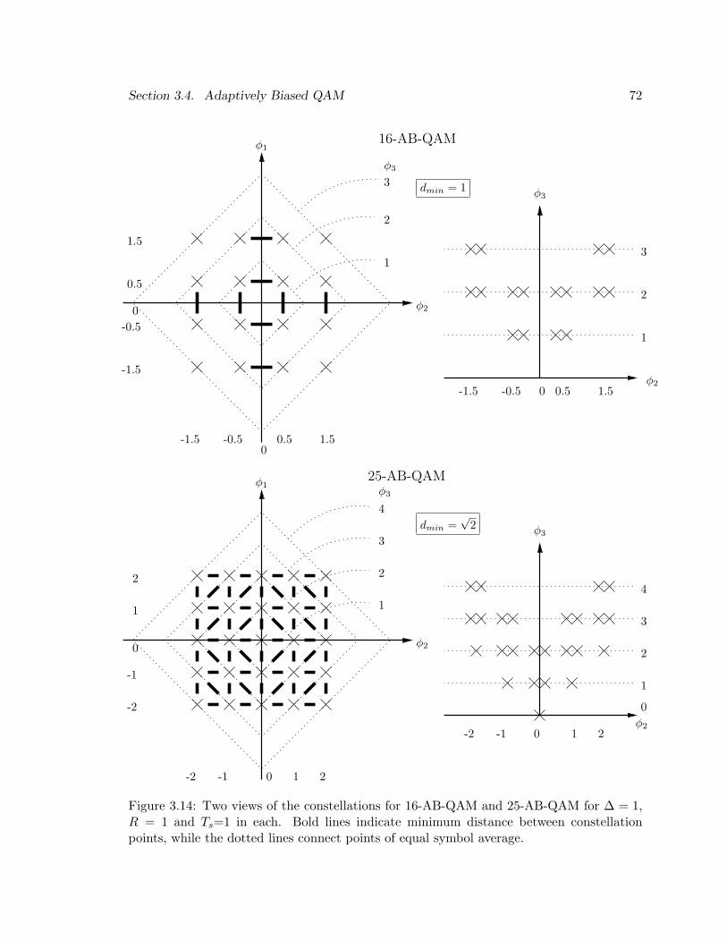
Section 3.4. Adaptively Biased QAM 72
1.5
0
φ1
φ3
φ2
-1.5 -0.5 0.50
-1.5
-0.5
0.5
1.5
1
2
3φ3
φ2
3
2
1
0 0.5 1.5-0.5-1.5
16-AB-QAM
dmin = 1
1
2
3
4φ3
0 21-2 -1
-2
-1
0
1
2
210-1-2
φ1
φ3
1
2
3
4
0φ2
25-AB-QAM
φ2
dmin =√
2
Figure 3.14: Two views of the constellations for 16-AB-QAM and 25-AB-QAM for ∆ = 1,R = 1 and Ts=1 in each. Bold lines indicate minimum distance between constellationpoints, while the dotted lines connect points of equal symbol average.

Section 3.4. Adaptively Biased QAM 73
0 10 20 30 40 50 60 7010
−6
10−4
10−2
100
Pe(s
ym)
L2
simulatedapprox.
Figure 3.15: Comparison of simulated symbol error rates to approximations in (3.35) and(3.37), with Ts=1 s, P=1 W, R=0.9 and σ2
n = 10−2 W/Hz.
This is analogous to the case of an even sized AB-PAM constellation. The distance between
points at the boundary in the three dimensional signal space is the same as the distance of
the points in the φ1-φ2 plane. As a result, there is no gain in exploiting the signal space
diversity inherent in AB-QAM for L2-even constellations. The CFM for L2-AB-QAM can
be written as,
CFMAB−QAM =2√
2R
L
√log2 L
Rb(3.36)
where L2 is even. The probability of symbol error can be determined approximately as,
Pe(sym) ≈ 4L·Q
(RP
L
√1
Rsσ2n
)+ 6 ·Q
(√2RP
L
√1
Rsσ2n
). (3.37)
The AB-QAM modulation scheme described in (3.27) was simulated using the channel model
of Figure 3.1. The symbol error rates were determined for a variety of constellation sizes.
Assuming that the random processes in the simulation are ergodic, the symbol error rate
can be used to estimate the probability of symbol error. Figure 3.15 presents a comparison
between the simulated symbol error rate and the approximates for Pe(sym) presented in
this section. The approximations on Pe(sym) based on the geometry of the constellation
closely approximate the simulated error rates.
The gain of AB-QAM over PAM, ΓAB−Q, can be determined using the same
methodology as was used to compute the gain for AB-PAM. The two dimensional gain,
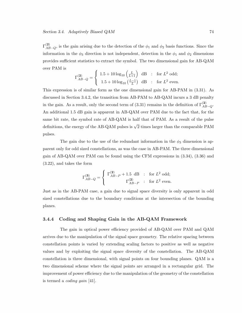
Section 3.4. Adaptively Biased QAM 74
Γ(2)AB−Q, is the gain arising due to the detection of the φ1 and φ2 basis functions. Since the
information in the φ3 direction is not independent, detection in the φ1 and φ2 dimensions
provides sufficient statistics to extract the symbol. The two dimensional gain for AB-QAM
over PAM is
Γ(2)AB−Q =
1.5 + 10 log10
(L
L+1
)dB : for L2 odd;
1.5 + 10 log10
(L−1
L
)dB : for L2 even.
This expression is of similar form as the one dimensional gain for AB-PAM in (3.31). As
discussed in Section 3.4.2, the transition from AB-PAM to AB-QAM incurs a 3 dB penalty
in the gain. As a result, only the second term of (3.31) remains in the definition of Γ(2)AB−Q.
An additional 1.5 dB gain is apparent in AB-QAM over PAM due to the fact that, for the
same bit rate, the symbol rate of AB-QAM is half that of PAM. As a result of the pulse
definitions, the energy of the AB-QAM pulses is√
2 times larger than the comparable PAM
pulses.
The gain due to the use of the redundant information in the φ3 dimension is ap-
parent only for odd sized constellations, as was the case in AB-PAM. The three dimensional
gain of AB-QAM over PAM can be found using the CFM expressions in (3.34), (3.36) and
(3.22), and takes the form
Γ(3)AB−Q =
Γ(2)AB−P + 1.5 dB : for L2 odd;
Γ(2)AB−P : for L2 even.
Just as in the AB-PAM case, a gain due to signal space diversity is only apparent in odd
sized constellations due to the boundary conditions at the intersection of the bounding
planes.
3.4.4 Coding and Shaping Gain in the AB-QAM Framework
The gain in optical power efficiency provided of AB-QAM over PAM and QAM
arrives due to the manipulation of the signal space geometry. The relative spacing between
constellation points is varied by extending scaling factors to positive as well as negative
values and by exploiting the signal space diversity of the constellation. The AB-QAM
constellation is three dimensional, with signal points on four bounding planes. QAM is a
two dimensional scheme where the signal points are arranged in a rectangular grid. The
improvement of power efficiency due to the manipulation of the geometry of the constellation
is termed a coding gain [41].

Section 3.4. Adaptively Biased QAM 75
Another means of improving the power efficiency of a modulation scheme is by
the selection of constellation points from a lattice to minimise the power requirements. In
conventional channels, a constellation is formed as a subset of points chosen from an infinite
lattice of points, such that the average energy of the constellation is minimised. For an N -
dimensional modulation scheme, this is done by bounding all the constellation points within
an N -dimensional sphere, since this surface has the lowest average energy encompassing a
given volume [54]. This gain is known as a shaping gain [41].
In optical intensity channels, a similar principle can be applied to minimise the
amount of average optical power. Using the framework defined in Section 3.1.3, a single
basis function, φavg in (3.9), is used to determine the average power of each symbol. In order
to minimise the average optical amplitude of the modulation scheme, each individual symbol
average should be minimised, following (3.8). Since the symbol averages are represented in
one dimension, this suggests that all symbols should occupy the lowest average power level
possible. Therefore, determining the optimum enclosing boundary for intensity channels is
a one dimensional problem, and symbol points must be chosen from the underlying lattice
such that they occupy the lowest possible coordinates in the φavg dimension.
Constellation shaping can be applied to the array of points defined for odd sized
AB-QAM constellations. These constellations consist of points on four bounding planes,
with signal points at the interface between planes. The minimum distance for these con-
stellations is due to the spacing of points within the underlying lattice of each plane, as
described in Section 3.4.2. Figure 3.14 shows the constellation for 25-AB-QAM. In keeping
with the paradigm of assigning constellation points to the lowest possible symbol averages,
the four constellation points with the highest average of 4 can be moved into the lower aver-
age power level with an average of 3. This is possible by moving these points to the (φ1, φ2)
coordinates (3, 0), (0, 3), (−3, 0) and (0,−3) as seen in Figure 3.16. This new shaped 25-
AB-QAM constellation requires less average optical power for the same minimum distance.
This improvement in the CFM over AB-QAM described in Section 3.4.2 is denoted as the
shaping gain Γs.
The shaping gain can be quantified by noting that for an L2 sized constellation,
the points are assigned such that the lowest levels of average optical power are filled. This
is equivalent to stating that points are assigned so that the φ3 coordinate value of each
constellation point is minimised. Therefore, the assignment of points can proceed from
the point of view of starting at the φ3 = 0 average plane, and filling points in lower
Section 3.4. Adaptively Biased QAM 76
φ3
1
2
3
0 21-2 -1
-2
-1
0
1
2
φ1
φ2
3-3
-3
3
Γs = 0.3 dB
Figure 3.16: Shaped constellation for 25-AB-QAM for ∆ = 1, R = 1 and Ts=1 in each.
average planes before a higher average plane is used. For an L2-AB-QAM constellation,
the minimum number of unique average levels required other than zero is denoted N , and
takes the form
N =
⌈√2L2 − 1− 1
2
⌉
where dye denotes the smallest integer not smaller than y. This expression is derived
assuming that the points are assigned so that the zero and the first N −1 average levels are
filled with the N th level filled to satisfy the L2 points of the constellation. It can be shown
that the shaping gain over the specified AB-QAM constellation in Section 3.4.2 takes the
form
Γs =
10 log10
(3L2
N(3L2−1)−2N3L2−12L
)dB : for L odd
10 log10
(3L2
N(3L2−1)−2N3L2−12L
)+ 1.5 dB : for L even
. (3.38)
The fixed gain of 1.5 dB is added to even sized constellations since in the case of unshaped
AB-QAM no gains are derived from the signal space diversity of the constellation. Using
the array of points contained in all odd sized AB-QAM constellations, and choosing a
subset with an even number of points ensures that this coding gain is present for even sized
constellations as well.
Section 3.4. Adaptively Biased QAM 77
Using the shaping gain expression in (3.38), the shaping gain available for 25-AB-
QAM is Γs = 0.3 dB. Figure 3.17 shows the constellation for 64-AB-QAM after shaping.
The gain due to shaping in this case is Γs = 1.75 dB. A majority of this gain is due to the
availability of coding gain using the information in the φ3 basis.
The complexity of the receiver for a multilevel modulation scheme can be measured
by the number of distinct output amplitudes which are generated. For any AB-QAM
constellation, the number of discrete levels in the output is equal to the number of unique
symbol averages possible. This is due to the fact that in AB-QAM the symbol average is
the sum of the individual phase magnitudes. Therefore, every possible amplitude which can
be generated by the scheme must have a corresponding DC bias term to ensure its non-
negativity. For the L2-AB-QAM modulation scheme of Section 3.4.2 the number of symbol
averages possible is L for odd size constellations and L−1 for even sized constellations. With
shaping gain, N + 1 distinct average values are present in the constellation. The shaped
constellation has a smaller number of output levels, and hence complexity, for L ≥ 3 except
L = 4.
Therefore, a shaping gain is possible for AB-QAM by using the set of all points
contained in odd sized AB-QAM constellations and choosing constellation points with the
minimum average optical power requirements. Constellations with an even number of points
benefit from this techniques not only through the efficiency of the shaping but also due to
the availability of coding gain.
3.4.5 Spectral Characteristics
As was done for the other modulation schemes, the frequency characteristics of the
AB-QAM, as defined in Section 3.4.1, were investigated using the power spectral density.
Using (3.17) the psd of L2-AB-QAM was found to be
GAB−QAM (f) =
(RP )2δ(f)− Ts(RP )2
2sinc2(πfTs)
+2TsA
2(RP )2(L + 1)3(L− 1)
2 sinc2(πfTs) + sinc2
(π2 fTs
)
− (1 + cos
(π2 fTs
))sinc(πfTs) sinc
(π2 fTs
)
,
where A is defined in (3.28). Figure 3.18 illustrates the power spectral density of 25-AB-
QAM. The bandwidth, as defined as the first spectral null, can be shown to be at f = 2/Ts.

Section 3.4. Adaptively Biased QAM 78
φ1
φ2
φ3
3
4
1
2
5
6
0 1-1 2 3 4 5 6-2-3-4-5
1
2
3
4
5
6
0
-1
-2
-3
-4
-5
-6
Γs = 1.75 dB
Figure 3.17: Shaped constellation for 64-AB-QAM for ∆ = 1, R = 1 and Ts=1 in each.
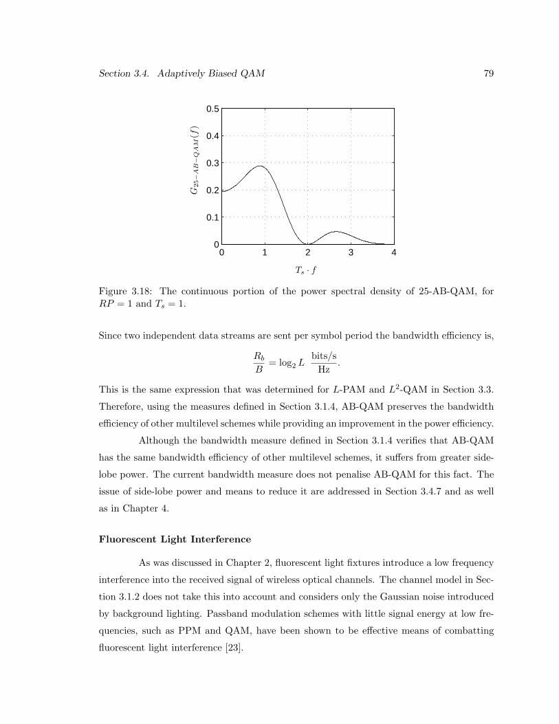
Section 3.4. Adaptively Biased QAM 79
0 1 2 3 40
0.1
0.2
0.3
0.4
0.5
G25−
AB−
QA
M(f
)
Ts · f
Figure 3.18: The continuous portion of the power spectral density of 25-AB-QAM, forRP = 1 and Ts = 1.
Since two independent data streams are sent per symbol period the bandwidth efficiency is,
Rb
B= log2 L
bits/sHz
.
This is the same expression that was determined for L-PAM and L2-QAM in Section 3.3.
Therefore, using the measures defined in Section 3.1.4, AB-QAM preserves the bandwidth
efficiency of other multilevel schemes while providing an improvement in the power efficiency.
Although the bandwidth measure defined in Section 3.1.4 verifies that AB-QAM
has the same bandwidth efficiency of other multilevel schemes, it suffers from greater side-
lobe power. The current bandwidth measure does not penalise AB-QAM for this fact. The
issue of side-lobe power and means to reduce it are addressed in Section 3.4.7 and as well
as in Chapter 4.
Fluorescent Light Interference
As was discussed in Chapter 2, fluorescent light fixtures introduce a low frequency
interference into the received signal of wireless optical channels. The channel model in Sec-
tion 3.1.2 does not take this into account and considers only the Gaussian noise introduced
by background lighting. Passband modulation schemes with little signal energy at low fre-
quencies, such as PPM and QAM, have been shown to be effective means of combatting
fluorescent light interference [23].
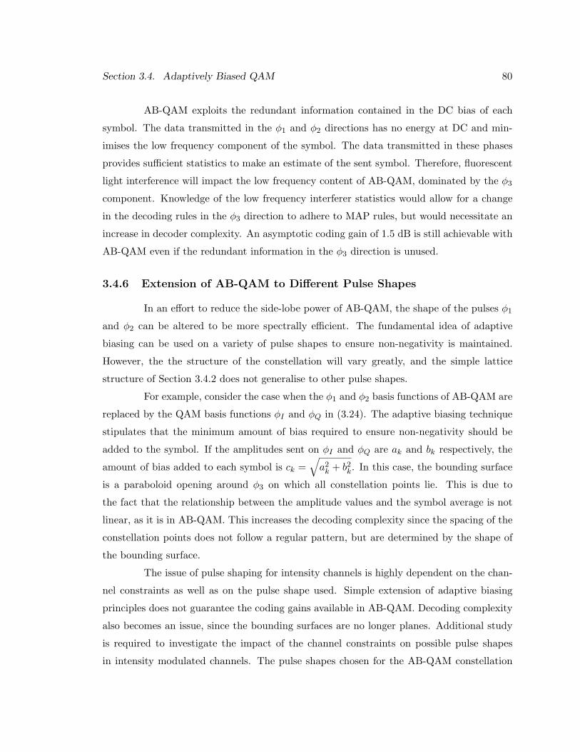
Section 3.4. Adaptively Biased QAM 80
AB-QAM exploits the redundant information contained in the DC bias of each
symbol. The data transmitted in the φ1 and φ2 directions has no energy at DC and min-
imises the low frequency component of the symbol. The data transmitted in these phases
provides sufficient statistics to make an estimate of the sent symbol. Therefore, fluorescent
light interference will impact the low frequency content of AB-QAM, dominated by the φ3
component. Knowledge of the low frequency interferer statistics would allow for a change
in the decoding rules in the φ3 direction to adhere to MAP rules, but would necessitate an
increase in decoder complexity. An asymptotic coding gain of 1.5 dB is still achievable with
AB-QAM even if the redundant information in the φ3 direction is unused.
3.4.6 Extension of AB-QAM to Different Pulse Shapes
In an effort to reduce the side-lobe power of AB-QAM, the shape of the pulses φ1
and φ2 can be altered to be more spectrally efficient. The fundamental idea of adaptive
biasing can be used on a variety of pulse shapes to ensure non-negativity is maintained.
However, the the structure of the constellation will vary greatly, and the simple lattice
structure of Section 3.4.2 does not generalise to other pulse shapes.
For example, consider the case when the φ1 and φ2 basis functions of AB-QAM are
replaced by the QAM basis functions φI and φQ in (3.24). The adaptive biasing technique
stipulates that the minimum amount of bias required to ensure non-negativity should be
added to the symbol. If the amplitudes sent on φI and φQ are ak and bk respectively, the
amount of bias added to each symbol is ck =√
a2k + b2
k. In this case, the bounding surface
is a paraboloid opening around φ3 on which all constellation points lie. This is due to
the fact that the relationship between the amplitude values and the symbol average is not
linear, as it is in AB-QAM. This increases the decoding complexity since the spacing of the
constellation points does not follow a regular pattern, but are determined by the shape of
the bounding surface.
The issue of pulse shaping for intensity channels is highly dependent on the chan-
nel constraints as well as on the pulse shape used. Simple extension of adaptive biasing
principles does not guarantee the coding gains available in AB-QAM. Decoding complexity
also becomes an issue, since the bounding surfaces are no longer planes. Additional study
is required to investigate the impact of the channel constraints on possible pulse shapes
in intensity modulated channels. The pulse shapes chosen for the AB-QAM constellation
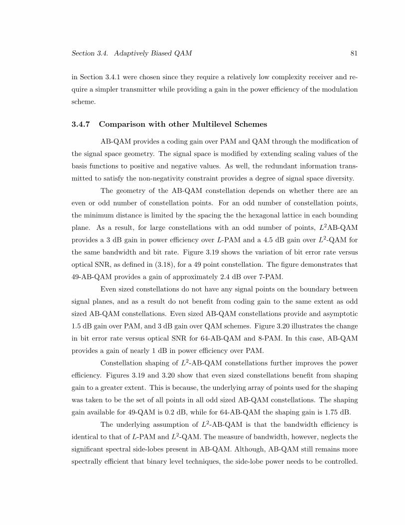
Section 3.4. Adaptively Biased QAM 81
in Section 3.4.1 were chosen since they require a relatively low complexity receiver and re-
quire a simpler transmitter while providing a gain in the power efficiency of the modulation
scheme.
3.4.7 Comparison with other Multilevel Schemes
AB-QAM provides a coding gain over PAM and QAM through the modification of
the signal space geometry. The signal space is modified by extending scaling values of the
basis functions to positive and negative values. As well, the redundant information trans-
mitted to satisfy the non-negativity constraint provides a degree of signal space diversity.
The geometry of the AB-QAM constellation depends on whether there are an
even or odd number of constellation points. For an odd number of constellation points,
the minimum distance is limited by the spacing the the hexagonal lattice in each bounding
plane. As a result, for large constellations with an odd number of points, L2AB-QAM
provides a 3 dB gain in power efficiency over L-PAM and a 4.5 dB gain over L2-QAM for
the same bandwidth and bit rate. Figure 3.19 shows the variation of bit error rate versus
optical SNR, as defined in (3.18), for a 49 point constellation. The figure demonstrates that
49-AB-QAM provides a gain of approximately 2.4 dB over 7-PAM.
Even sized constellations do not have any signal points on the boundary between
signal planes, and as a result do not benefit from coding gain to the same extent as odd
sized AB-QAM constellations. Even sized AB-QAM constellations provide and asymptotic
1.5 dB gain over PAM, and 3 dB gain over QAM schemes. Figure 3.20 illustrates the change
in bit error rate versus optical SNR for 64-AB-QAM and 8-PAM. In this case, AB-QAM
provides a gain of nearly 1 dB in power efficiency over PAM.
Constellation shaping of L2-AB-QAM constellations further improves the power
efficiency. Figures 3.19 and 3.20 show that even sized constellations benefit from shaping
gain to a greater extent. This is because, the underlying array of points used for the shaping
was taken to be the set of all points in all odd sized AB-QAM constellations. The shaping
gain available for 49-QAM is 0.2 dB, while for 64-AB-QAM the shaping gain is 1.75 dB.
The underlying assumption of L2-AB-QAM is that the bandwidth efficiency is
identical to that of L-PAM and L2-QAM. The measure of bandwidth, however, neglects the
significant spectral side-lobes present in AB-QAM. Although, AB-QAM still remains more
spectrally efficient that binary level techniques, the side-lobe power needs to be controlled.
Section 3.4. Adaptively Biased QAM 82
15 20 2510
−20
10−15
10−10
10−5
100
Bit
Err
orR
ate
OSNR (dB)
PAM
QAM
AB-QAMShaped
AB-QAM
Figure 3.19: Comparison of bit error rates versus optical signal-to-noise ratio for 49-QAM,7-PAM, 49-AB-QAM and shaped 49-AB-QAM (R = 1 A/W, σ2
n = 10−2 W/Hz, B = 2 Hzand Rb = log2(49) bits/s).
15 20 2510
−20
10−15
10−10
10−5
100
Bit
Err
orR
ate
OSNR (dB)
ShapedAB-QAM
AB-QAM
QAM
PAM
Figure 3.20: Comparison of bit error rates versus optical signal-to-noise ratio for 64-QAM,8-PAM, 64-AB-QAM and shaped 64-AB-QAM (R = 1 A/W, σ2
n = 10−2 W/Hz, B = 2 Hzand Rb = 6 bits/s).

Section 3.5. Conclusions and Comparison 83
Pulse shaping techniques present an interesting avenue of future research to accomplish this
goal. Chapter 4 presents a constrained coding approach which aims to further improve the
spectral efficiency of modulation schemes on intensity channels.
3.5 Conclusions and Comparison
The need for bandwidth efficient modulation schemes is motivated by the use of
inexpensive optoelectronic devices for wireless optical links. Binary level schemes, although
power efficient, do not provide a high degree of bandwidth efficiency. As a result, multilevel
schemes, which trade-off power efficiency for bandwidth efficiency are investigated.
A multilevel modulation scheme, adaptively biased QAM, is proposed which pre-
serves the bandwidth of PAM and QAM while providing a gain in power efficiency. The
use of shaping gain to further improve the power efficiency has also been discussed in the
framework established for intensity modulated channels in this chapter.
In order to compare the various modulation schemes discussed in the chapter, the
constellation figure of merit is used. The gain of each modulation scheme relative to on-off
keying was calculated as a metric of comparison. OOK was chosen as a reference point
due to its simplicity of implementation, and pervasiveness in conventional communications.
Formally, the gain ΓOOK is defined as,
ΓOOK = 10 log10
(CFMx
CFMOOK
)
where CFMx is the constellation figure of merit for modulation scheme under consideration.
In order to capture the spectral performance of each scheme as well, ΓOOK is plotted versus
the bandwidth efficiency for various sized constellations in Figure 3.21.
The optimal point for any modulation scheme destined for wireless optical links
would be in the upper right hand corner of the figure, where bandwidth efficiency and power
efficiency are maximised. Binary level techniques offer the best power efficiency at the
cost of reduced bandwidth efficiency. Multilevel schemes provide the necessary bandwidth
efficiency for wireless optical links at the cost of power efficiency. AB-QAM maintains the
bandwidth efficiency of other multilevel techniques while improving on the power efficiency.
The use of constellation shaping techniques provides significant gains in the power efficiency
of AB-QAM, especially for even sized constellations. The use of even sized constellations
which are powers of 2 is commonly used in binary data communication systems.

Section 3.5. Conclusions and Comparison 84
0 0.5 1 1.5 2 2.5 3
−8
−6
−4
−2
0
2
4
6
OOKPulses in appendix AL-PPM
L2-AB-QAMShaped L2-AB-QAM
L2-QAML-PAM
2
6
33
6
49
64
64
64
9
3
16
16
16
8
9
M = 2
ΓO
OK
(dB
)
Bandwidth Efficiency Rb/B
Figure 3.21: Comparison of power efficiency gain of modulation schemes over OOK plottedversus bandwidth efficiency.

Section 3.5. Conclusions and Comparison 85
The focus of this chapter has been to develop means of improving the power effi-
ciency of existing multilevel techniques. Although AB-QAM does provide an improvement
in the power efficiency over other multilevel techniques, significant spectral side-lobes are
present. In order to achieve the high bandwidth efficiencies required by high speed wireless
optical links, spectrally efficient pulses must be used on intensity modulated channels.
Chapter 4
Constrained Coding Techniques for
Intensity Modulated Channels
The optical intensity channel imposes constraints on the type of signals which may
be transmitted. Chapter 3 discusses the physical channel constraints imposed by the nature
of information transmission using an optical intensity signal. The use of inexpensive optical
components along with the requirement for high data rates imposes an added constraint of
high bandwidth efficiency. Conventional schemes satisfy the channel constraints through
the careful selection of the pulse shapes used. As a result, the choice of pulse shapes which
are bandwidth efficient cannot be made independently of the channel constraints.
This chapter introduces a novel means of satisfying the channel constraints of the
optical intensity channel. Well-developed techniques of constrained coding are applied to
ensure that the non-negativity constraint is met when using bandwidth efficient pulses in
the optical intensity channel. Basic elements of constrained coding are reviewed and the
mathematical constructs of symbolic dynamics are introduced. The general concepts are
applied to an intensity modulated channel using an example and compared to a simple
baseline. A coder is developed using well known techniques, and issues involved in the
construction of practical encoders and decoders are briefly discussed.
4.1 Motivation
Coding techniques have been used for some time to surmount physical constraints
imposed by a communications channel. In magnetic disk channels, runlength-limited codes
86

Section 4.1. Motivation 87
are used to ensure the minimum and maximum number of consecutive “1” or “0” symbols
recorded. If the transitions between symbols are too close together, intersymbol inter-
ference will occur due to the proximity of the magnetic domains on the disk. However,
transitions between the symbol levels must occur with a guaranteed periodicity to ensure
timing synchronisation is maintained [55, 56]. In channels where the signals are capacitor
or transformer coupled to the receiver, baseline wander is introduced. This effect is due to
the fact that AC coupling introduces a zero at DC which causes intersymbol interference to
be introduced into the signal. So called charge-constrained codes ensure that the running
digital sum is bounded, minimising the baseline wander interference [41, 57].
The goal of this chapter is to propose and demonstrate the use of similar con-
strained coding techniques for the intensity modulated channel. The non-negativity con-
straint (3.1) specifies that the channel constraint applies to the transmitted intensity wave-
form x(t). The definition of x(t) is contained in (3.5), which states simply that the intensity
waveform over all time is composed of the addition of symbol functions for each interval. The
previous chapter assumed that each symbol was time limited and non-negative throughout
a symbol period in order to ensure that the non-negativity constraint was met. However,
this is an overly conservative assumption since the non-negativity constraint applies to the
sum of the symbol pulses and not to each individual symbol function. If a PAM type mod-
ulation scheme is considered, the non-negativity constraint can be satisfied by choosing a
bandwidth efficient pulse which is non-zero outside the symbol interval and constraining
the scaling factors so that the sum of the symbol pulses remains non-negative. The aver-
age optical power transmitted can then be controlled by a scaling factor dependent on the
output data distribution.
The impact of using coding techniques to satisfy the non-negativity constraint can
be illustrated by looking at the case of Nyquist pulses. Nyquist pulses are a set of functions
which introduce no intersymbol interference to the transmission. In a conventional channel,
the minimum bandwidth Nyquist pulse occupies a bandwidth of B = 1/Ts Hz, where
Ts is the symbol period. However, Appendix B shows that in an intensity channel the
minimum bandwidth of a non-negative Nyquist pulse occupies twice this bandwidth or B =
2/Ts Hz. Therefore, the imposition of the non-negativity constraint increased the minimum
bandwidth required for Nyquist pulses. On the other hand, 1/Ts Hz bandwidth Nyquist
pulses can be used on an intensity modulated channel if a coding scheme is developed so that
the choice of scaling factors ensures that the summation of all symbols remains non-negative

Section 4.2. Constrained Coding and Symbolic Dynamics 88
for all time.
The remainder of the chapter describes the development of constrained codes for
a pulse amplitude modulated type scheme with a family of pulse shapes. Before discussing
the application of constrained coding techniques to the intensity modulated channel, the
basic framework for the development of these codes is presented.
4.2 Constrained Coding and Symbolic Dynamics
Channels which do not permit certain sequences of symbols to be sent due to
physical or practical limitations are referred to as constrained channels or input-restricted
channels. The channel constraints are taken to be deterministic and invariant in time. The
role of the channel coder, or constrained coder, is to take an unrestricted input sequence
and transform it into a constrained sequence which satisfies all of the channel restrictions.
The development of constrained codes can be analysed using the mathematics
of symbolic dynamics. Symbolic dynamics deals with the transformation and analysis of
fundamental units known as shift spaces. Shift spaces are composed of bi-infinite sequences
of symbols chosen from a finite alphabet A. A block is a finite length sequence of symbols
chosen over A. Constraints are introduced by specifying a set F of forbidden blocks, none of
which may appear as a sub-block of any sequence in the shift space. The forbidden blocks,
in the case of an optical intensity channel, correspond to sequences of symbols which are
not transmittable in the channel. A shift space, X, is defined as a bi-infinite sequence of
symbols chosen over a finite alphabet A such that no sub-block is contained in the set F .
For the systems considered in this chapter, the set F is finite, and hence the shift spaces
considered are called shifts of finite type.
Shifts of finite type in which every block in F is of length M +1 are called M -step
shifts. In this type of shift space, it is only necessary to look at the past M symbols to
detect whether a forbidden block was sent. In other words, the system has a memory of
M symbols. It can be shown that any shift of finite type, X, can be represented as a
directed graph, G. If the labelling of the edges in G is taken from A, the resulting shift
is known in literature as a sofic shift [55]. The connection of the vertices in the graph is
determined so that the sequence of edges traversed in any bi-infinite walk through the graph
form X. Explicitly, every element of the shift space X corresponds to some infinite walk
in the graph G. In this manner, analysis of the shift space X can be performed using the

Section 4.2. Constrained Coding and Symbolic Dynamics 89
model represented by the graph G.
The graph G, which represents the shift space is composed of a set of L vertices
from the vertex set V interconnected by a set of edges. The topology of the graph can be
represented in the form of an N ×N non-negative, integer matrix known as the adjacency
matrix. Without loss of generality we assume that the vertices are numbered from the set
of natural numbers such that V = 1, 2, 3, . . . , N. If I, J ∈ V are two vertices in the graph,
let aIJ denote the number of edges originating at vertex I and terminating at vertex J . The
adjacency matrix of a graph is composed of the set of all aIJ in the form A = [aIJ ]. The
adjacency matrix determines the structure of the graph, but neglects the labelling of the
edges. The graphs considered in this chapter have the property that no two edges leaving
a given vertex carry the same labelling. This type of graph is known as a right-resolving
presentation, and it can be shown that every sofic shift has this type of presentation [55].
The entropy of the shift space is a measure of the maximum amount of information
that can be represented in the messages coded according to the rules of the space. For
noiseless, discrete channels, this measure can be thought of as the capacity of the channel,
since it determines the upper bound on the amount of information which can be represented
in the shift. The entropy of a shift space X is defined as
h(X) ∆= limn→∞
1n
log2 |Bn(X)|, (4.1)
where |Bn(X)| is the number of blocks of length n which occur in the shift X [55]. This
definition is analogous to the definition for the capacity of a noiseless discrete channel given
by Shannon [58], and can be thought of as the capacity of the channel as imposed by the
structure of the shift space.
The notion of entropy can be related to the directed graph representation of the
shift space. The fundamental definition of the entropy of the shift space can be written
using the adjacency matrix of the graph. The entropy of a shift X is
h(X) = log2 λ (4.2)
where λ is the largest, real eigenvalue of the adjacency matrix A, satisfying
Av = λv (4.3)
for the corresponding eigenvector v. The existence of λ > 0 for the adjacency matrices con-
sidered in this chapter is guaranteed by the Perron-Frobenius Theorem [55]. The calculated

Section 4.2. Constrained Coding and Symbolic Dynamics 90
entropy of X in (4.1) and (4.2) is often referred to as the topological entropy of the shift
space [59]. This terminology is more precise since conventional definitions of entropy rely
on probabilistic distributions while the entropy of the shift space, as defined, depends only
on the structure of the shift space itself. As a result, the topological entropy is determined
by the structure of the shift space and sets the upper bound on the entropy of all messages
arising from the space.
The probabilistic nature of data transmission can be incorporated into the graph
model of the shift space. If the vertices of the graph are viewed as a set of states, S, and if
transition probabilities are assigned to each edge, the resulting structure is a discrete-time
Markov process. The probability of making a transition to state j given that the current
state is i is denoted qij , where i, j ∈ S. Assuming that S is chosen in the same way as V, the
collection of all transition probabilities forms an N × N state transition matrix Q = [qij ].
The matrix Q is a stochastic matrix since its row sums are all unity, or formally,
N∑
j=1
qij = 1
for every i = 1, 2, 3, . . . , N . Given a starting state, so ∈ S, the process chooses one of the
outgoing edges according to the transition probabilities. At each transition, a symbol value
is output corresponding to the edge labelling. The maximum entropy of the output messages
is the topological entropy of the underlying graph. Assuming no multiple edges between
pairs of states, as is the case in the graphs considered in this chapter, the maxentropic state
transition matrix, Q, can be determined in terms of its elements qij as,
qij = Prnext state = j | current state = i = aij1λ
vj
vi, (4.4)
where aij are the elements of A and v = [v1, v2, . . . , vN ]T, λ are defined in (4.3) [56]. To
summarise, if the state transition probabilities in (4.4) are used, the entropy of the resulting
Markov chain will be equal to the topological entropy of the shift space defined in (4.2).
The Markov chain derived from the graphs presented in this chapter is homoge-
neous since the channel constraints are fixed and deterministic. Additionally, it can be
shown that the Markov chain is fully regular [55, 47]. In this case, the stationary distri-
bution vector, Π, is independent of the starting state, and illustrates the probability of
being in a given state. The stationary distribution vector, Π, can be determined from the
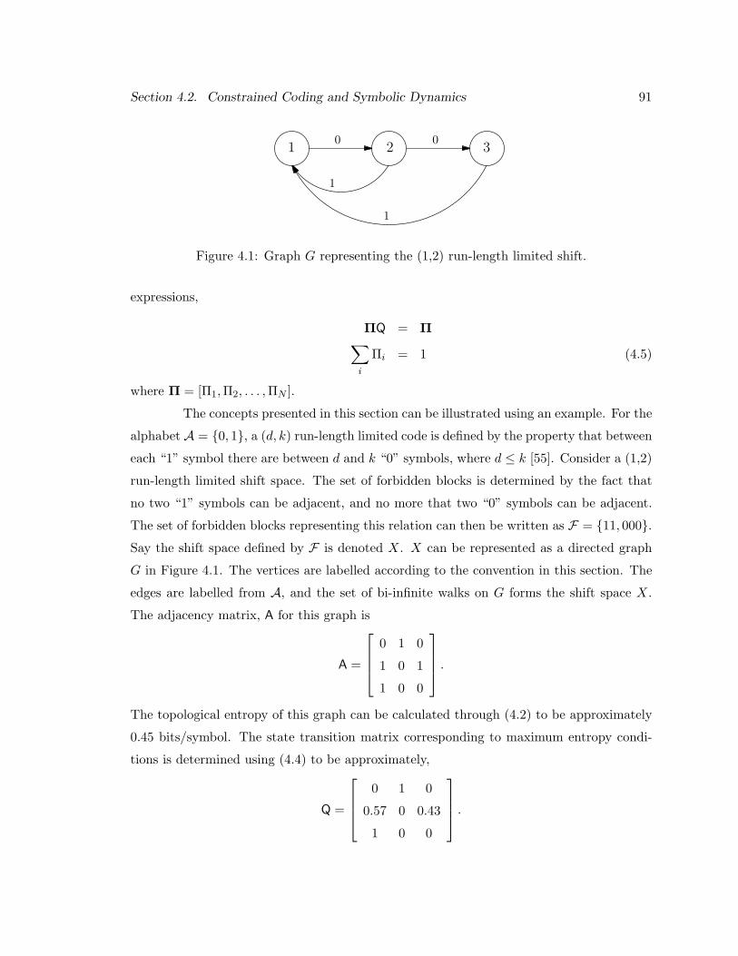
Section 4.2. Constrained Coding and Symbolic Dynamics 91
1 2 3
1
1
0 0
Figure 4.1: Graph G representing the (1,2) run-length limited shift.
expressions,
ΠQ = Π∑
i
Πi = 1 (4.5)
where Π = [Π1, Π2, . . . , ΠN ].
The concepts presented in this section can be illustrated using an example. For the
alphabet A = 0, 1, a (d, k) run-length limited code is defined by the property that between
each “1” symbol there are between d and k “0” symbols, where d ≤ k [55]. Consider a (1,2)
run-length limited shift space. The set of forbidden blocks is determined by the fact that
no two “1” symbols can be adjacent, and no more that two “0” symbols can be adjacent.
The set of forbidden blocks representing this relation can then be written as F = 11, 000.Say the shift space defined by F is denoted X. X can be represented as a directed graph
G in Figure 4.1. The vertices are labelled according to the convention in this section. The
edges are labelled from A, and the set of bi-infinite walks on G forms the shift space X.
The adjacency matrix, A for this graph is
A =
0 1 0
1 0 1
1 0 0
.
The topological entropy of this graph can be calculated through (4.2) to be approximately
0.45 bits/symbol. The state transition matrix corresponding to maximum entropy condi-
tions is determined using (4.4) to be approximately,
Q =
0 1 0
0.57 0 0.43
1 0 0
.

Section 4.3. A Constrained Code for Intensity Modulated Channels 92
The stationary distribution vector for this Q is Π =[0.41 0.41 0.18].
This section aims to provide a brief overview of some central concepts in symbolic
dynamics as applied to the examples in this chapter. More complete references cataloguing
the links between symbolic dynamics and coding can be found elsewhere in the literature
[55, 59, 60, 57].
4.3 A Constrained Code for Intensity Modulated Channels
4.3.1 Introduction
In an effort to control the spectral characteristics of a modulation scheme band-
width efficient pulses are employed. In PAM, spectrally efficient pulses such as raised-cosine
pulses are used to control the amount of bandwidth occupied by each pulse and minimise
the out of band power.
The goal of the constrained coding technique in this chapter is to exploit similar
bandwidth efficient pulses on an intensity modulated channel. Indeed, the same raised-
cosine pulses could be employed on an intensity modulated channel if a suitable constrained
coder could be constructed to ensure that the resulting collection of pulses remains non-
negative for all time.
In order to initiate study into the applicability of constrained coding for intensity
modulated channels, a simplified discrete time channel model is employed. The channel
is set as being discrete in order to simplify the computation requirements required for the
example, while preserving some meaning in the results. This discrete case can be looked
upon as a bounding case for a set of continuous functions where non-negativity at the
sample points of the output implies global non-negativity of the function. Additionally, the
channel is taken as being noiseless to determine the maximum possible information transfer
rate.
This section presents a discrete time example of constrained coding applied to the
non-negativity constraint for intensity modulated channels. We present the structure of the
pulses along with the procedure used to determine the performance of the coding scheme.
Comparisons to a low complexity baseline scheme are presented in the same framework to
determine the possible gains available from the constrained coding technique.
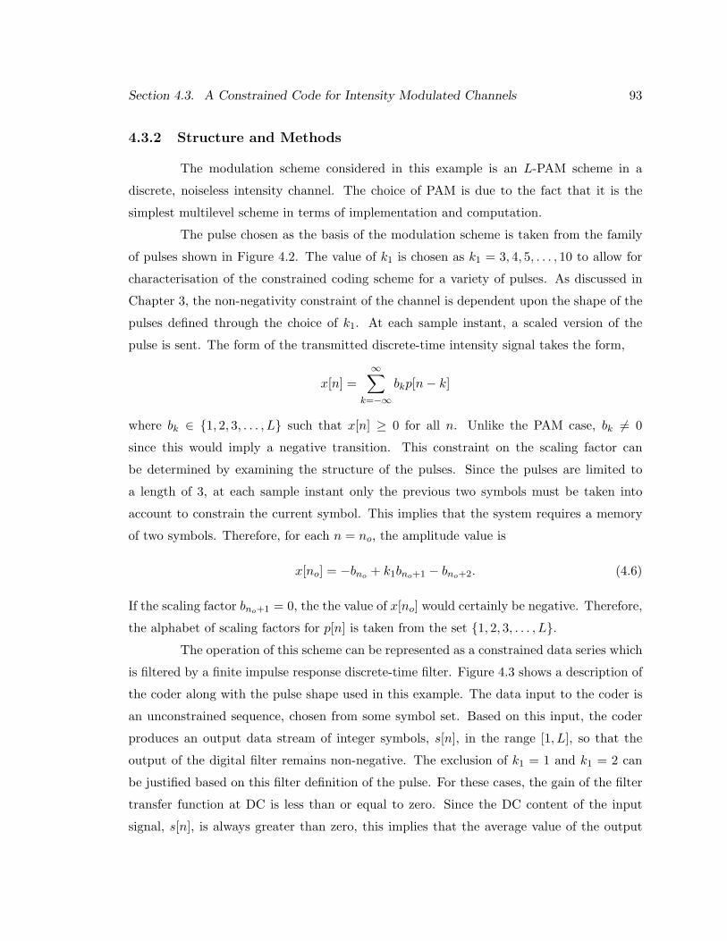
Section 4.3. A Constrained Code for Intensity Modulated Channels 93
4.3.2 Structure and Methods
The modulation scheme considered in this example is an L-PAM scheme in a
discrete, noiseless intensity channel. The choice of PAM is due to the fact that it is the
simplest multilevel scheme in terms of implementation and computation.
The pulse chosen as the basis of the modulation scheme is taken from the family
of pulses shown in Figure 4.2. The value of k1 is chosen as k1 = 3, 4, 5, . . . , 10 to allow for
characterisation of the constrained coding scheme for a variety of pulses. As discussed in
Chapter 3, the non-negativity constraint of the channel is dependent upon the shape of the
pulses defined through the choice of k1. At each sample instant, a scaled version of the
pulse is sent. The form of the transmitted discrete-time intensity signal takes the form,
x[n] =∞∑
k=−∞bkp[n− k]
where bk ∈ 1, 2, 3, . . . , L such that x[n] ≥ 0 for all n. Unlike the PAM case, bk 6= 0
since this would imply a negative transition. This constraint on the scaling factor can
be determined by examining the structure of the pulses. Since the pulses are limited to
a length of 3, at each sample instant only the previous two symbols must be taken into
account to constrain the current symbol. This implies that the system requires a memory
of two symbols. Therefore, for each n = no, the amplitude value is
x[no] = −bno + k1bno+1 − bno+2. (4.6)
If the scaling factor bno+1 = 0, the the value of x[no] would certainly be negative. Therefore,
the alphabet of scaling factors for p[n] is taken from the set 1, 2, 3, . . . , L.The operation of this scheme can be represented as a constrained data series which
is filtered by a finite impulse response discrete-time filter. Figure 4.3 shows a description of
the coder along with the pulse shape used in this example. The data input to the coder is
an unconstrained sequence, chosen from some symbol set. Based on this input, the coder
produces an output data stream of integer symbols, s[n], in the range [1, L], so that the
output of the digital filter remains non-negative. The exclusion of k1 = 1 and k1 = 2 can
be justified based on this filter definition of the pulse. For these cases, the gain of the filter
transfer function at DC is less than or equal to zero. Since the DC content of the input
signal, s[n], is always greater than zero, this implies that the average value of the output
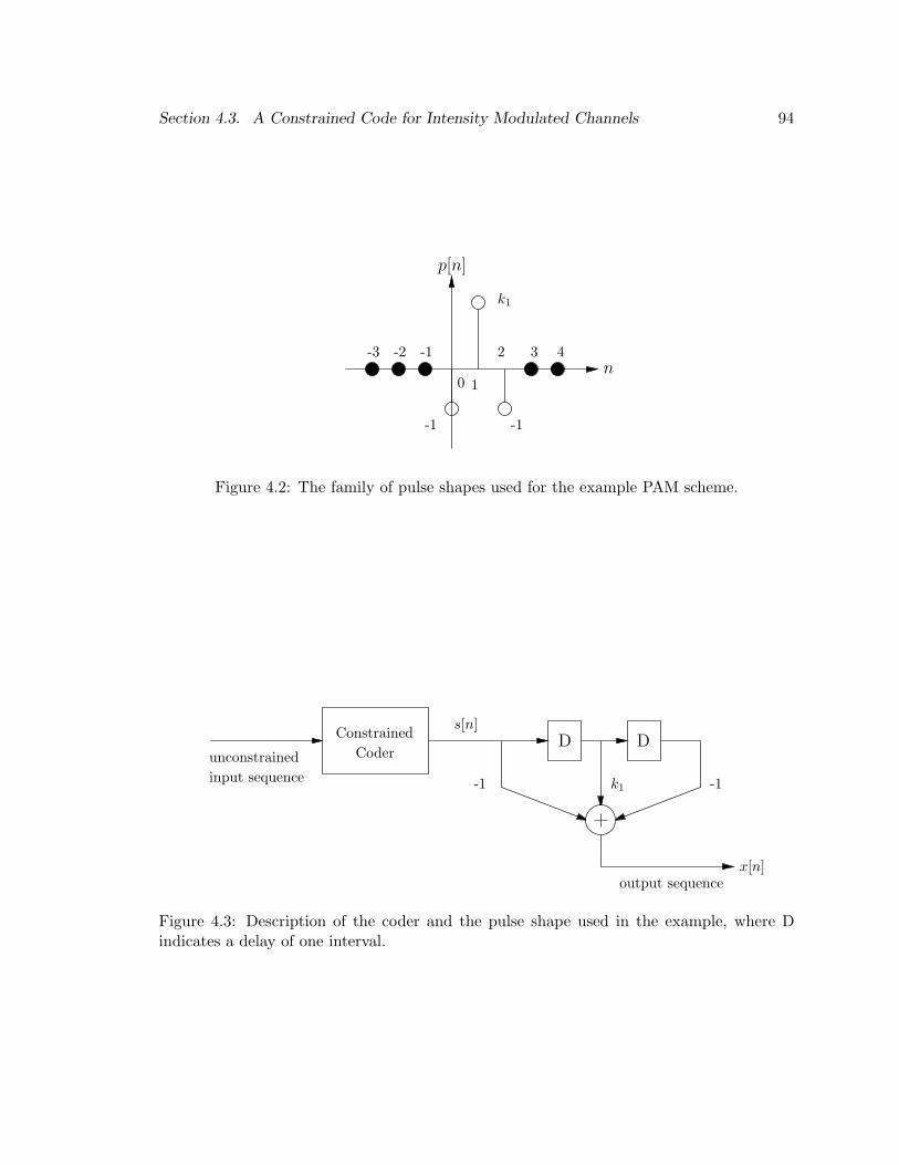
Section 4.3. A Constrained Code for Intensity Modulated Channels 94
k1
-1
-1
-1
0
-2-3
1
32 4n
p[n]
Figure 4.2: The family of pulse shapes used for the example PAM scheme.
D DConstrainedCoderunconstrained
input sequence
s[n]
output sequencex[n]
-1 -1k1
Figure 4.3: Description of the coder and the pulse shape used in the example, where Dindicates a delay of one interval.

Section 4.3. A Constrained Code for Intensity Modulated Channels 95
is zero or negative. A zero average value implies that zero is sent at every instant, while a
negative average is impermissible.
The parameters L and k1 completely describe a modulation scheme in the form of
that in Figure 4.3. In order to determine the maximum amount of information that a given
scheme can send, the techniques in Section 4.2 must be employed.
Define a shift space, X, which is determined by the set of forbidden blocks F ,
where symbols are chosen from the alphabet A = 1, 2, 3, . . . , L. The bi-infinite sequence
generated through X is used to define the signal s[n] at the input of the filter in Figure
4.3. The blocks in F can be seen as the set of inputs which cause negative transitions in
x[n]. Since the system has a memory of two symbols, each of the forbidden blocks can
be represented as length three blocks. The number of blocks in F is finite since both the
alphabet and memory of the system are finite. Therefore, X is a 2-step shift of finite type
and can be represented by a directed graph G.
The graph G can be determined by specifying a set of L2 vertices, V, corresponding
to the set of all length 2 blocks over A. These 2-blocks correspond to possible values for
the filter state and are represented as the ordered pair Ψi = [ψ1i, ψ2i] where Ψi ∈ V and
i ∈ 1, 2, 3, . . . , L2. The edges interconnecting the vertices are determined according to the
non-negativity constraint of the channel as determined by the filter transfer function. An
edge exists between state Ψi and Ψj if and only if the inequality
−ψ1j + k1ψ1i − ψ2i ≥ 0 (4.7)
is satisfied. Let eij = ψ1j for those edges which exist. Due to this construction, for a
given state there is at most one edge leading to any other state since each of the Ψi are
unique. The adjacency matrix corresponding to G, A, can be determined based on the
above structure.
Once the adjacency matrix is formed, A is simplified by removing unnecessary
states. All vertices with zero indegree or outdegree can be pruned from the graph. These
states represent discontinuities in the bi-infinite shift space represented by the graph, and
are not permitted. An adjacency matrix which has vertices with outdegree and indegree of
at least one is termed essential. Similarly, all vertices with an outdegree of one with self
loops were eliminated. These states are called “black hole” states since once entered, there
is no sequence of inputs to escape the state. These states can be removed since they provide

Section 4.3. A Constrained Code for Intensity Modulated Channels 96
no information to the output message. After pruning, let the number of states remaining
be N ≤ L2.
Using the adjacency matrix, the topological entropy of the graph can be calculated
via (4.2) for each L and k1.
The average power constraint in (3.2), fixes the distribution of the amplitude values
of the output. In this discrete channel, it is necessary to determine the expected value
of the sequence x[n] for some probability distribution. Using the maxentropic transition
probabilities in (4.4) to form Q, ensures that the average amplitude calculated corresponds
to the case where the entropy of the output message is equal to the topological entropy of
the graph. Using the state transition matrix, Q, the stationary distribution vector in (4.5) is
calculated. The Πi are the steady-state probability of being in a given state. The transition
between states i and j in Q represents the output of a symbol, and occurs with probability
Πiqij . Visiting every element of Q, the expected value of x[n] can then be written in the
form,
Ex[n] =N∑
i=1
N∑
j=1
(−eij + k1ψ1i − ψ2i) ·Πiqij . (4.8)
Note that qij = 0 if there is no edge between states Ψi and Ψj , and so the inconsistency in
the eij definition is removed.
4.3.3 Results
The topological entropy and the average of each modulation scheme defined by k1
and L are calculated according to the guidelines in Section 4.3.2.
Figure 4.4 shows a plot of the topological entropy of each modulation scheme over
k1 and L. The function h(X)max = log2 L plotted in the figure represents the maximum
capacity of a noiseless channel using L symbols. The distance from every curve in Figure
4.4 to the h(X)max curve indicates the number of bits/symbol lost due to the channel
constraints. This loss of capacity is due to the sequences of symbols which must be excluded
due to the non-negativity constraint. The figure indicates that the penalty reduces as the
k1 term of the pulse increases. For a fixed L, the alphabet A of all the schemes is the same.
The inequality in (4.7), demonstrates that for a fixed alphabet increasing k1 increases the
number of points which satisfy the inequality. Qualitatively, the amount of DC bias of
each symbol is increased as k1 increases. This added bias term allows more flexibility in
the choice of symbols since the negative components of each pulse become less significant
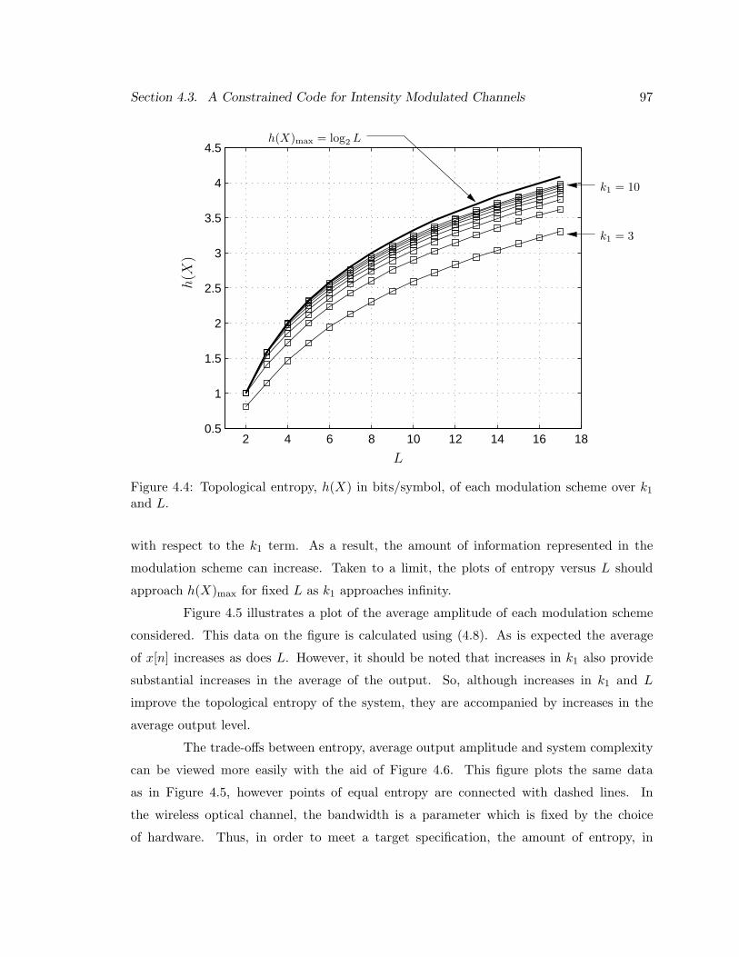
Section 4.3. A Constrained Code for Intensity Modulated Channels 97
2 4 6 8 10 12 14 16 180.5
1
1.5
2
2.5
3
3.5
4
4.5
h(X
)
L
h(X)max = log2 L
k1 = 3
k1 = 10
Figure 4.4: Topological entropy, h(X) in bits/symbol, of each modulation scheme over k1
and L.
with respect to the k1 term. As a result, the amount of information represented in the
modulation scheme can increase. Taken to a limit, the plots of entropy versus L should
approach h(X)max for fixed L as k1 approaches infinity.
Figure 4.5 illustrates a plot of the average amplitude of each modulation scheme
considered. This data on the figure is calculated using (4.8). As is expected the average
of x[n] increases as does L. However, it should be noted that increases in k1 also provide
substantial increases in the average of the output. So, although increases in k1 and L
improve the topological entropy of the system, they are accompanied by increases in the
average output level.
The trade-offs between entropy, average output amplitude and system complexity
can be viewed more easily with the aid of Figure 4.6. This figure plots the same data
as in Figure 4.5, however points of equal entropy are connected with dashed lines. In
the wireless optical channel, the bandwidth is a parameter which is fixed by the choice
of hardware. Thus, in order to meet a target specification, the amount of entropy, in

Section 4.3. A Constrained Code for Intensity Modulated Channels 98
2 4 6 8 10 12 14 16 180
10
20
30
40
50
60
70
80
Ex
[n]
L
k1 = 3
k1 = 10
Figure 4.5: Average output amplitude of each modulation scheme over k1 and L.
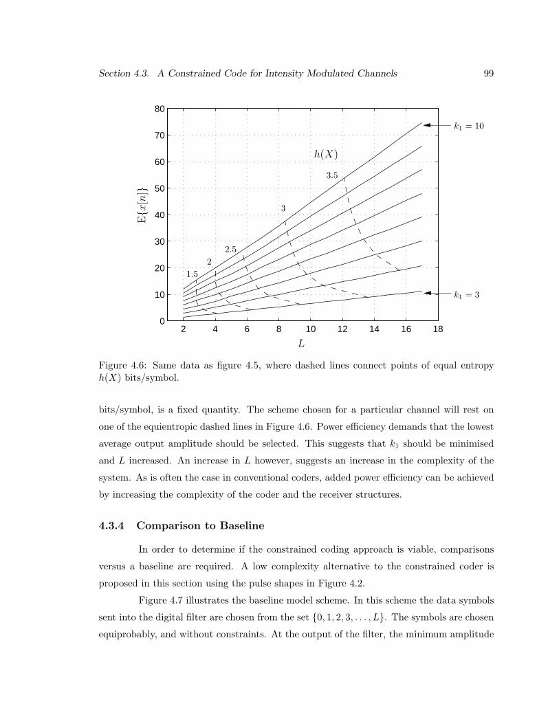
Section 4.3. A Constrained Code for Intensity Modulated Channels 99
2 4 6 8 10 12 14 16 180
10
20
30
40
50
60
70
80
Ex
[n]
L
k1 = 3
k1 = 10
3.5
h(X)
3
2.52
1.5
Figure 4.6: Same data as figure 4.5, where dashed lines connect points of equal entropyh(X) bits/symbol.
bits/symbol, is a fixed quantity. The scheme chosen for a particular channel will rest on
one of the equientropic dashed lines in Figure 4.6. Power efficiency demands that the lowest
average output amplitude should be selected. This suggests that k1 should be minimised
and L increased. An increase in L however, suggests an increase in the complexity of the
system. As is often the case in conventional coders, added power efficiency can be achieved
by increasing the complexity of the coder and the receiver structures.
4.3.4 Comparison to Baseline
In order to determine if the constrained coding approach is viable, comparisons
versus a baseline are required. A low complexity alternative to the constrained coder is
proposed in this section using the pulse shapes in Figure 4.2.
Figure 4.7 illustrates the baseline model scheme. In this scheme the data symbols
sent into the digital filter are chosen from the set 0, 1, 2, 3, . . . , L. The symbols are chosen
equiprobably, and without constraints. At the output of the filter, the minimum amplitude

Section 4.3. A Constrained Code for Intensity Modulated Channels 100
D Dunconstrainedinput sequence
s[n]
-1 -1k1
2Loutput sequence
x[n]
Figure 4.7: Description of the baseline scheme.
value possible is −2L. As a result, a fixed bias added to the output ensure that the non-
negativity constraint is met.
The maximum entropy available from this scheme is equal to the entropy of the
data symbols entering the filter. Since the alphabet of input sources consists of L + 1
symbols, the entropy of the messages arising from the baseline case is H = log2(L + 1).
Due to the fact that the amplitude values are chosen equiprobably, it can be shown that
the expected value of the output amplitude for the baseline case is
Ex[n] =k1 + 2
2L.
The comparison between the baseline case and the constrained coding technique of
Section 4.3.2 is done using the fact that the output discrete signals represent and intensity
function. Hence the expected value of the output amplitude is really a measure of the
average optical power transmitted. For a given entropy, the gain G is defined as,
G∆= 10 log10
Pbaseline
Pcoded
where P represents the average optical power required for the baseline and coded schemes.
Figure 4.8 plots this comparison for k1 = 3, 4, 5, . . . , 10.
The figure demonstrates that constrained coding has the greatest benefits over the
baseline as the entropy required increases and as k1 decreases. The essential trade-off of
the constrained coder is that it takes a given pulse shape and a number of levels L such
that log2 L is greater than the entropy of the data to be coded. Through the structure of
the constrained coder, the excess entropy of system is traded to ensure that the channel
constraints are met. The addition of excess L in large k1 schemes is costly to the average

Section 4.3. A Constrained Code for Intensity Modulated Channels 101
0.5 1 1.5 2 2.5 3 3.5 4
−3
−2
−1
0
1
2
3
G(d
B)
h(X)
k1 = 3
k1 = 10
Figure 4.8: Power gain G (dB) of constrained coding technique over baseline case versustopological entropy, h(X) in bits/symbol.
Section 4.3. A Constrained Code for Intensity Modulated Channels 102
optical power budget due to their inherent high DC content. In the low k1 case, the addition
of levels requires less average optical power than adding a bias to each symbol ensure non-
negativity. As a result, Figure 4.8 indicates that constrained coding is advantageous over
the baseline for small k1, at the cost of increased number of levels and complexity.
4.3.5 Code Construction
The constrained coder accepts an unconstrained input sequence and outputs a
sequence which meets the channel constraints. In order to implement the constrained
systems discussed in Section 4.3.2, a coder must be designed. In the example presented
in Figure 4.3, the constrained coder is designed so that the output sequence remains non-
negative once filtered by the digital filter corresponding to the pulse shape. This section
presents an example of a code which satisfies the non-negativity constraint for a given pulse
shape and L.
Let a modulation scheme be defined by the pulse shape in Figure 4.2 with k1 = 3
and where the alphabet is set by L = 4. Assume that the input symbols are chosen from
the binary alphabet Ain = 0, 1 with equal probability. This corresponds to the types of
signals commonly used in data communications. It is also assumed that the input symbols
are grouped in blocks of length p, while the output symbols are grouped in blocks of length
q. The constrained coder performs a mapping from the set of p length binary input blocks
to the set of q length blocks over A = 1, 2, 3, . . . , L.The topological entropy of the defined system is h(X) ≈ 1.46 bits/symbol, as
shown in Figure 4.4. The amount of information that can be coded in the output sequence
must be less than the topological entropy of the shift space. This follows directly from
Shannon’s channel coding theorem, where the data transfer rate must be less than or equal
to the channel capacity for lossless transmission of data. The constraint on the amount of
information which can be transmitted in the k1 = 3, L = 4 system can be written in terms
of the input and output block sizes as,
h(X) ≥ p
q.
Stated in words, the topological entropy of the underlying graph must be greater than or
equal to the number of bits/symbol encoded in the output sequence. Integer values for p
and q are chosen so that their ratio satisfies the inequality. The choice of p and q affects the

Section 4.3. A Constrained Code for Intensity Modulated Channels 103
complexity of the coder design, and determines the coder latency. In this example, p = 4
and q = 3 yielding a 4b-3s coder : four input bits map to a three symbol output sequence.
The formulation of the structure of the coder was performed using a well know
technique known as the ACH algorithm [59, 55]. This algorithm provides a set of guidelines
which direct a series of state splittings of a higher order edge shift. At each step of the algo-
rithm decisions are made which can affect the final form of the coder. Heuristic techniques
are used to ensure that like states are merged at every step to minimise the complexity of
the implementation.
In the end, the algorithm produces a state transition diagram, where the outdegree
of every state is equal to 2p. Figure 4.9 presents the state transition diagram for the
example 4b-3s code after applying the ACH algorithm. The branches of the state transition
diagram are labelled with the input sequence and output sequence corresponding to each
transition. For compactness, the sequences of four input bits are represented by the integer
set 0, 1, 2, 3, . . . , 15 through the traditional binary to decimal number system relationship.
At each transition one of the 16 edges leaving each state is selected by the input sequence.
The assignment of four bit input sequences to each edge, also known as the input road-
colouring, determines the implementation complexity of the coder and is discussed in Section
4.3.6.
Using the 4b-3s coder defined in this section, Figure 4.10 shows a series of se-
quences at various point in the model presented in Figure 4.3. The input sequence is
an unconstrained equiprobable sequence of binary symbols represented in decimal format.
The output of the coder consists of the symbols taken from A according to the channel
constraints. The output sequence remains non-negative over the period of the simulation,
as stipulated by the coder.
4.3.6 Decoder Structure
The implementation of the constrained code as given by the state transition di-
agram in Figure 4.9 depends on the assignment of the input symbol values to each edge.
The set of labellings corresponding to the input values which choose an edge to be followed
is know as the input road-colouring of the coder.
The input road-colouring has no impact on whether the channel constraints are
satisfied. The code is structured so that any walk through the state transition diagram
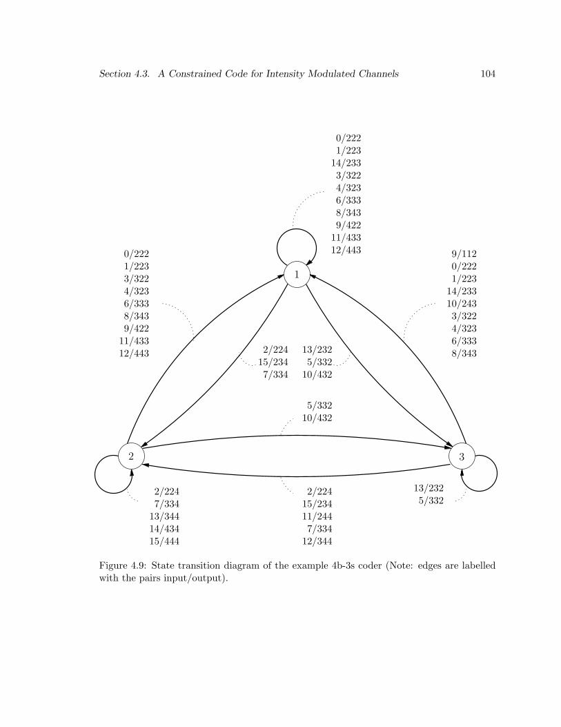
Section 4.3. A Constrained Code for Intensity Modulated Channels 104
1
2 3
0/2221/223
14/2333/3224/3236/3338/3439/422
11/43312/443 9/112
0/2221/223
14/23310/2433/3224/3236/3338/343
0/2221/2233/3224/3236/3338/3439/422
11/43312/443 2/224
15/2347/334
13/2325/332
10/432
5/33210/432
2/22415/23411/2447/334
12/344
13/2325/332
2/2247/334
13/34414/43415/444
Figure 4.9: State transition diagram of the example 4b-3s coder (Note: edges are labelledwith the pairs input/output).

Section 4.3. A Constrained Code for Intensity Modulated Channels 105
0 50 100 150 200 2500
5
10
15
0 100 200 300 400 500 600 7000
1
2
3
4
0 100 200 300 400 500 600 700
0
2
4
6
8
Input
sequen
cex[n
]s[
n]
(a)
(b)
(c)
n
n
n
Figure 4.10: Critical signals in the 4b-3s code example : (a) the input sequence (in decimalformat), (b) the output of the coder, (c) the output intensity signal of the filter.

Section 4.3. A Constrained Code for Intensity Modulated Channels 106
results in output sequences which are transmittable.
At the receiver a structure is necessary to decode the received symbols. The
decoder must perform the inverse mapping of the coder to arrive at the binary symbols
transmitted in the channel. A straightforward way in which to accomplish this decoding
is to use the same state machine in the decoder as was used in the coder. The output of
the decoder in this scheme depends on the input as well as an internal state variable. If
some of the transmitted symbols are corrupted by noise, the internal state variable may
also become corrupted. In theory, one incorrect symbol detected may permanently corrupt
the internal state, causing every input sequence to be decoded incorrectly. This situation
is known as infinite error propagation.
A class of decoders known as sliding block decoders alleviate this infinite error
propagation problem. The data input to the decoder is broken into a series of blocks of
length q symbols, where the block and instant n is denoted xn. At instant n, the decoder
mapping function f maps the input blocks to a decoded binary block of length p, which is
denoted bn. This mapping can be represented as
bn = f(xn−a, . . . , xn, . . . , xn+m)
where m is known as the memory of the decoder and a is the anticipation of the decoder.
Therefore, the data is decoded using only the input sequence of symbol blocks. An error
in decoding a given block propagates a distance of m + a + 1 blocks which is known as the
window length of the decoder. This sliding block decoder can be implemented with the
prudent choice of input road-colouring.
Table 4.1 shows the relationships between received and decoded symbol blocks
which define a sliding block decoder for the 4b-3s code of Section 4.3.5. The input to the
decoder is a set of blocks of length q = 3, chosen over A. The memory of the decoder is one
block and the anticipation is zero. Therefore an error in detecting a block will propagate
for two input blocks to the decoder, or for eight output bits. The entries in table 4.1
are grouped according to the states from which they originate. There are 22 unique edge
labellings for the coded data, which originate from the 3 states. No two edges coming from
a given state can share the same input or output labellings. The input labellings assigned to
each unique edge value depend on the states from which these edges can be generated. For
the edge “334”, the input labelling depends on the value of the previous block. Analysis of
the graph in Figure 4.9 shows that in this case, the previous block received at the decoder

Section 4.3. A Constrained Code for Intensity Modulated Channels 107
u v r Relationship222 ∗ 0223 ∗ 1224 ∗ 2322 ∗ 3323 ∗ 4 Edges from all states332 ∗ 5333 ∗ 6334 ∗ 7343 ∗ 8422 ∗ 9432 ∗ 10 Edges from states433 ∗ 11 1 and 2443 ∗ 12232 ∗ 13233 ∗ 14
Edges from states
234 ∗ 151 and 3
434 ∗ 14 Edges from state444 ∗ 15 2 only112 ∗ 9243 ∗ 10
Edges from state
244 ∗ 113 only
334 224 13334 234 13334 244 13334 334 13
Edges from self-loop
334 344 13of state 2
334 434 13334 444 13334 232 12334 332 12
Edges from state
334 432 123 to 2
Table 4.1: Sliding block decoder for 4b-3s code considered in the example. u is the currentinput block and v is the previous input block. r is the decoded block of binary datarepresented in decimal format. The entries denoted by “∗” indicate that any block may bereceived in this interval.
Section 4.4. Conclusions 108
gives information about the previous state of the decoder. This fact is used to differentiate
the two possible decoded values for this state.
The final structure of the sliding block decoder is heavily dependent on the choice
of actions during the code formation and decoder determination. Decisions at every step of
code construction process can lead to different structures for the coder structure. The size
of the decoding window as well dependent on the process used to derive the code.
4.4 Conclusions
This chapter has introduced the concept of using constrained coding techniques
to satisfy the non-negativity constraint in wireless optical channels. The use of constrained
coding eliminates the assumption that non-negative pulses must be used, and applies the
constraint directly to the intensity function. This scheme has applications in the use of
bandwidth efficient pulses, which do not remain non-negative, but whose sum can be con-
strained to be non-negative.
The example of a constrained code applied to a discrete optical channel shows that
constrained coding techniques are able to satisfy channel constraints over a family of pulses.
The inherent trade-off in using constrained coding is an increase in complexity over simpler
baseline cases. The formulation of coder and decoder structures using the ACH algorithm
is highly dependent on decisions made during at each step of the algorithm. Heuristic
techniques are used to achieve lower complexity implementations.
The use of a discrete channel as an example was adopted to reduce the complexity
of the calculations required for the formulation of the coder. The results of this example
apply directly to the set of continuous time functions of length three symbol periods where
non-negativity at the sampling instants of the output signal ensures that the signal remains
non-negative between instants. If this set of functions is used to bound the amplitudes
of practical bandwidth efficient pulses, conservative estimates on performance are possible
from this framework. Additional study is necessary to apply this work to a more general
class of continuous time pulses.
This chapter is intended as an introduction to the concept of using constrained
coding to satisfy the constraints of an optical channel. To the knowledge of the author,
this is the first suggestion of using constrained coding to implement modulation schemes
on wireless optical channels. Further work is required to extend these results to a set of
bandwidth efficient pulses suitable for implementation.
Chapter 5
Conclusions and Future Directions
5.1 Conclusions
Wireless optical links are a viable solution to the problem of short distance, high
data rate connections. These links have advantages over mechanical and RF wireless tech-
niques due to their flexibility and low cost. The channel characteristics of a wireless optical
channel differ significantly from those in conventional communications channels. Since the
data is sent as an intensity waveform, negative amplitudes are not possible. Additionally,
eye-safety constraints limit the average amplitude level of the signalling scheme.
In order to develop signalling schemes for the wireless optical channel, the channel
characteristics were investigated. The optoelectronic components used to generate and de-
tect the launched optical intensity signal are key determinants in the channel characteristics.
Light emitting diodes and p-i-n photodiodes are well suited to wireless optical applications
due to their low cost, high linearity and modest support circuitry requirements. Measure-
ments on an experimental channel were performed using typical optoelectronics indicating
that the wireless optical channel is limited by poor bandwidth and moderate linearity.
These effects are primarily due to the fact that inexpensive optical components are needed
to ensure that the proposed link has the widest field of application possible.
To surmount the channel constraints and limitations, the modulation scheme cho-
sen for the wireless optical channel must simultaneously provide good bandwidth and power
efficiency. Conventional modulation schemes for optical channels rely on binary level pulse
techniques which sacrifice bandwidth efficiency for power efficiency. Multilevel schemes pro-
vide high bandwidth efficiencies at the price of reduced power efficiency. Adaptively biased
109

Section 5.2. Future Directions 110
QAM is developed as a modulation scheme which preserves the high bandwidth efficiency
of other multilevel techniques while improving on the power efficiency. An asymptotic gain
of 3 dB is possible over PAM for large constellations. Constellation shaping was also shown
to provide added power savings, especially for even sized constellations.
The non-negativity constraint of the optical channel applies to the transmitted
intensity signal. Symbol pulses can be chosen so that they are spectrally efficient, so long as
the resulting sum of signals remains non-negative. The use of constrained coding techniques
allows for the selection of pulses which assume both positive and negative amplitudes while
satisfying the non-negativity constraint. This allows a degree of freedom in the choice of
pulse shape giving the system designer the ability to tradeoff of system complexity for
bandwidth efficiency or power efficiency.
5.2 Future Directions
The selection of optoelectronics determines the severity of the channel limitations.
The development of inexpensive, high bandwidth optoelectronics for the 1.55 µm infrared
wavelength would improve the channel constraints, allowing for simpler implementations.
The longer wavelength lessens the impact of the average optical power constraint as seen in
Chapter 2. Higher bandwidth devices would more easily accommodate the high data rates
required, and device structures which deliver these characteristics at low cost are required.
In addition to the development of advanced optoelectronics, models are required to
allow system designers to more accurately predict link performance. In order to formulate
a model for the optoelectronics, a sensitive design bench must be constructed to extract all
relevant properties of the devices. Calibrated light emitters along with receivers are required
to test the linear as well as non-linear performance of the LEDs as well as photodiodes.
The model for the optoelectronics would simplify the design of linearised transmitters and
receivers for future high speed links.
The development of pulse shaping techniques for intensity channels is also a nec-
essary next step. In an effort to improve the spectral performance of existing modulation
schemes, pulse shaping may be employed. The links between individual pulse shapes and
the channel constraints on the amplitude must be generalised in order to determine what
gains are possible with this technique. The concept of signal space diversity, introduced
in Chapter 3, fits in with the pulse shaping idea since the amount of bias for each symbol

Section 5.2. Future Directions 111
transmitted is intimately linked to the pulse shape. As a result, the use of redundant in-
formation in the average of each pulse transmitted can be used to improve the estimate of
the received symbol, improving power efficiency.
This thesis has introduced the notion of employing constrained coding techniques
to satisfy the non-negativity constraint of optical channels. Further generalisation of this
concept to a set of continuous time pulses is required, as well as a study of candidate pulse
shapes that optimise performance on the link. Simulation with an accurate channel model
of the link is required to explore the practicality of using constrained coding techniques in
optical channels.
Appendix A
Optimum Binary Pulse Set for
Average Constrained Channels
A.1 Introduction
Intensity modulated channels are limited by the fact that all signals must remain
positive for all time and that the average amplitude is limited. This appendix presents
a squared distance argument which is used to develop an optimum set of two signals for
binary signalling on an intensity channel.
A.2 Problem Definition
Let γ1(t) and γ2(t) be the two time domain representations of the intensity signal
set which are time limited to t ∈ [0, Ts], where Ts is the symbol interval. Furthermore,
assume that each symbol interval is divided into M disjoint time intervals of equal duration.
If the intensity is taken not to vary in each sub-interval, then the set of time functions in
which only one interval is non-zero may be taken as a set of basis functions of the functions
γ1(t) and γ2(t). More formally, the basis functions can be written as
φi(t) =√
M
Tsrect
(t− Ts/M(i− 1/2)
Ts/M
)(A.1)
where i = 1, 2, . . . , M and rect(·) is the rectangular window functions as defined in Section
3.2.
112
Section A.2. Problem Definition 113
The signals can be represented as a pair of L dimensional vectors, γ1 and γ2, in
the signal space defined by the φi(t) basis functions. These signal vectors can be broken
into a set of components to give
γ1 = γ11, γ12, . . . , γ1Mγ2 = γ21, γ22, . . . , γ2M. (A.2)
The channel constraints can now be applied to the components of γ1 and γ2.
The non-negativity constraint forces all of the components of the signal vectors to
be non-negative. Since the basis functions are always non-negative, the vector components
must satisfy
γij ≥ 0, i = 1, 2 j = 1, 2, 3, . . . , M.
The average amplitude constraint forces the average of the output signal to be
fixed. The average value of each signal, avg(γi) is specified as
avg(γi) =1Ts
∫ Ts
0γi(t) dt.
The expression for each symbol average can be simplified by re-writing γi in terms of its
basis functions, giving
avg(γi) =1Ts
∫ Ts
0
M∑
m=1
γimφm(t) dt.
Since both the summation and integration are over finite intervals, they can be exchanged
yielding,
avg(γi) =M∑
m=1
γim1Ts
∫ Ts
0φm(t) dt.
The average value of the amplitude of each basis function is the same, and is represented
as the constant Kφ. Simplifying the expression for symbol average gives,
avg(γi) = Kφ
M∑
m=1
γim. (A.3)
Assuming that the two signals are sent independently and equiprobably, the expected value
of the symbol averages is proportional to the sum of the symbol averages. If the average
amplitude of the modulation scheme is fixed at P , then the sum of the symbol averages can
be related to P through (A.3) as
2∑
i=1
M∑
m=1
γim ∝ P.
Section A.3. Development 114
So, the average amplitude constraint reduces to the following constraint on the sum of the
components of γ1 and γ22∑
i=1
M∑
m=1
γim = K
for some constant K.
Chapter 3 discusses how the distance between constellation points is indicative of
the reliability of transmission for a given modulation scheme. The figure of merit of a set of
signal points is taken as the square distance between them in the signal space. The optimal
scheme in this sense can be determined by maximising the distance between constellation
points subject to the channel constraints.
The non-negativity constraint and the limited average amplitude constraint are
then just limitations on the values and sum of the components of the signal vectors in the
defined signal space. Since the constraints and the objective function to maximise are vector
quantities, the problem definition is formulated as a generic vector problem.
Find :
γ1 and γ2 are two L dimensional vectors in a Euclidean L space. The components of these
vectors are given as in (A.2).
Find γ1 and γ1 such that ‖γ1 − γ2‖2 is maximised subject to the constraints :
1. γij ≥ 0, i = 1, 2 j = 1, 2, 3, . . . ,M
2.∑2
i=1
∑Mm=1 γim = K
A.3 Development
Since the channel constraints are written in terms of the co-ordinate values of the
vectors, the objective function is rewritten in terms of components values as,
‖γ1 − γ2‖2 =M∑
m=1
(γ1m − γ2m)2
Re-arranging the terms,
‖γ1 − γ2‖2 =M∑
m=1
γ21m + γ2
2m − 2M∑
m=1
γ1mγ2m
= ‖γ1 + γ2‖2 − 4 〈γ1, γ2〉 (A.4)
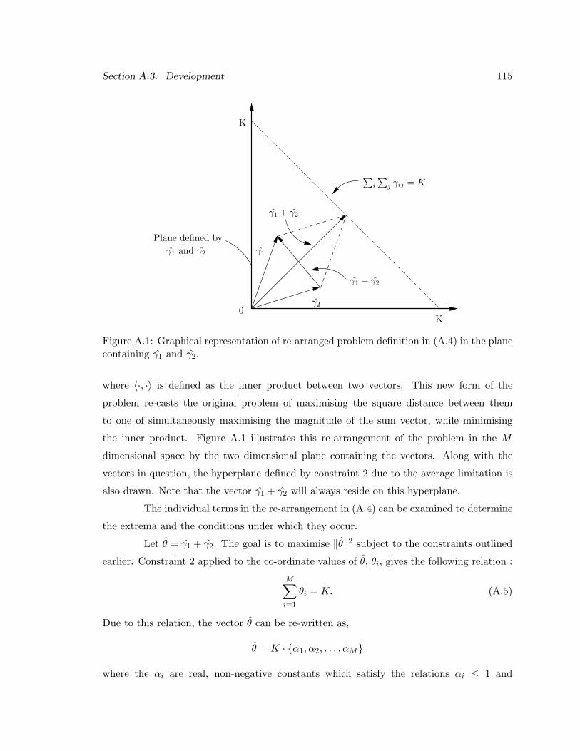
Section A.3. Development 115
Plane defined byγ1 and γ2 γ1
γ2
γ1 − γ2
γ1 + γ2
K
K0
∑i
∑j γij = K
Figure A.1: Graphical representation of re-arranged problem definition in (A.4) in the planecontaining γ1 and γ2.
where 〈·, ·〉 is defined as the inner product between two vectors. This new form of the
problem re-casts the original problem of maximising the square distance between them
to one of simultaneously maximising the magnitude of the sum vector, while minimising
the inner product. Figure A.1 illustrates this re-arrangement of the problem in the M
dimensional space by the two dimensional plane containing the vectors. Along with the
vectors in question, the hyperplane defined by constraint 2 due to the average limitation is
also drawn. Note that the vector γ1 + γ2 will always reside on this hyperplane.
The individual terms in the re-arrangement in (A.4) can be examined to determine
the extrema and the conditions under which they occur.
Let θ = γ1 + γ2. The goal is to maximise ‖θ‖2 subject to the constraints outlined
earlier. Constraint 2 applied to the co-ordinate values of θ, θi, gives the following relation :
M∑
i=1
θi = K. (A.5)
Due to this relation, the vector θ can be re-written as,
θ = K · α1, α2, . . . , αM
where the αi are real, non-negative constants which satisfy the relations αi ≤ 1 and

Section A.3. Development 116
∑Mi=1 αi = 1. An expression for ‖θ‖2 can be given by performing the operation
⟨θ, θ
⟩
to give,
‖θ‖2 = K2 ·M∑
i=1
α2i .
Since 0 ≤ αi ≤ 1 then α2i ≤ αi. So, if
∑Mi=1 αi = 1, then
∑Mi=1 α2
i ≤ 1. Applying this
inequality gives,
‖θ‖2 = K2 ·M∑
i=1
α2i ≤ K2. (A.6)
Therefore, max‖γ1 + γ2‖2 = K2.
The second term of the objective function in (A.4) consists of the inner product
between signal vectors γ1 and γ2. This inner product is the sum of a series of products
of corresponding co-ordinate values in the two vectors. Since all co-ordinate values are
constrained to be non-negative by constraint 1, the minimum sum possible is 0.
Using Figure A.1 and geometric intuition, the choice of γ1 and γ2 can be directed
by the expansion in (A.4). To achieve the minimum possible inner product, γ1 and γ2 must
be orthogonal. Additionally, to have the maximum possible magnitude for θ = γ1 + γ2,
from (A.6),M∑
i=1
α2i =
M∑
i=1
αi = 1.
This equality holds in the case that α2i = αi. In this case, the αi must be chosen from the set
0,1, where α2i = αi. Equation (A.5) implies that all the θi co-ordinates are zero except for
at one co-ordinate value, θio , where θio = K. From the definition, θio = γ1io + γ2io = K. If
the inner product 〈γ1, γ2〉 = 0, which is the minimum possible, this implies that γ1ioγ2io = 0,
since all other co-ordinate values are zero. The two constraints on the io co-ordinate values
can only be met if one co-ordinate is set to 0 while the other is set at K.
Therefore, setting the signal vectors γ1 and γ2 as
γ1 = 0
γ2 = v ∈ RM | vm = K · δmo ,v = vm,m = 1, 2, . . . , M, mo ∈ 1, 2, . . . ,M
simultaneously maximises the term ‖γ1 + γ2‖2 while minimising 〈γ1, γ2〉 of (A.4). This
implies that the above choice for signal vectors maximises the square distance between the
signal points while satisfying constraints 1 and 2.
Section A.3. Development 117
Using the basis functions in (A.1), a time domain representation for the signal
points can be given for t ∈ [0, Ts] as
γ1(t) = 0
γ2(t) = 2MP · rect(
t− Ts/M(i− 1/2)Ts/M
)(A.7)
for some i ∈ 1, 2, . . . , M.If these pulses were transmitted on the linear, Gaussian white noise limited chan-
nel described in Section 3.1.2, it is possible to determine key metrics to allow for comparison
with other schemes. For this optimal signalling set, the constellation figure of merit, de-
scribed in (3.14), can can be found to be,
CFMopt =2MR√MRb
(A.8)
where Rb = Rs = 1/Ts, as defined in Chapter 3. Similarly, the bandwidth efficiency can be
shown to beRb
B=
1M
bits/sHz
. (A.9)

Appendix B
Minimum Bandwidth,
Non-Negative Nyquist Pulse
B.1 Purpose
Optical intensity modulated channels impose the constraint that transmitted sig-
nals must remain non-negative for all time. This is due the the fact that optoelectronic
components can only modulate or detect the presence of an optical power signal. Since
data is transmitted as a power signal on the channel, no negative values are physically
possible.
In a conventional channel, the minimum bandwidth required for zero ISI trans-
mission is π/T rad/s (where T is the sampling period). The purpose of this appendix is to
identify the pulse which occupies the minimum bandwidth required to meet the Nyquist I
criterion while satisfying the optical channel non-negativity constraint.
B.2 Problem Definition
Let p(·) be a real valued, smooth, continuous function of time t, t ∈ R. Let p(t)
have a Fourier transform P (ω). Additionally, let p(t) satisfy the following constraints :
1. P (ω) = 0, for |ω| ≥ B, B > π/T .
2. p(kT ) = δk, where T is the sampling period, k ∈ I.
3. p(t) ≥ 0 ∀ t ∈ R.
118
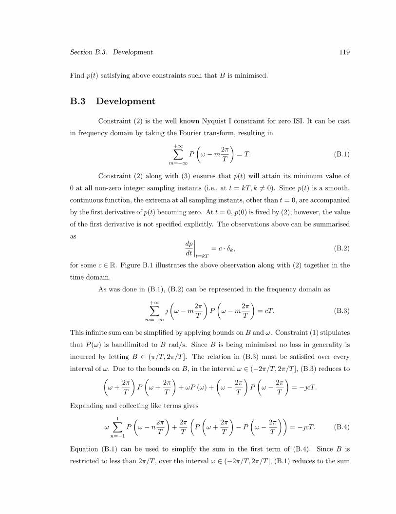
Section B.3. Development 119
Find p(t) satisfying above constraints such that B is minimised.
B.3 Development
Constraint (2) is the well known Nyquist I constraint for zero ISI. It can be cast
in frequency domain by taking the Fourier transform, resulting in
+∞∑m=−∞
P
(ω −m
2π
T
)= T. (B.1)
Constraint (2) along with (3) ensures that p(t) will attain its minimum value of
0 at all non-zero integer sampling instants (i.e., at t = kT, k 6= 0). Since p(t) is a smooth,
continuous function, the extrema at all sampling instants, other than t = 0, are accompanied
by the first derivative of p(t) becoming zero. At t = 0, p(0) is fixed by (2), however, the value
of the first derivative is not specified explicitly. The observations above can be summarised
asdp
dt
∣∣∣∣t=kT
= c · δk, (B.2)
for some c ∈ R. Figure B.1 illustrates the above observation along with (2) together in the
time domain.
As was done in (B.1), (B.2) can be represented in the frequency domain as
+∞∑m=−∞
(ω −m
2π
T
)P
(ω −m
2π
T
)= cT. (B.3)
This infinite sum can be simplified by applying bounds on B and ω. Constraint (1) stipulates
that P (ω) is bandlimited to B rad/s. Since B is being minimised no loss in generality is
incurred by letting B ∈ (π/T, 2π/T ]. The relation in (B.3) must be satisfied over every
interval of ω. Due to the bounds on B, in the interval ω ∈ (−2π/T, 2π/T ], (B.3) reduces to(
ω +2π
T
)P
(ω +
2π
T
)+ ωP (ω) +
(ω − 2π
T
)P
(ω − 2π
T
)= −cT.
Expanding and collecting like terms gives
ω
1∑
n=−1
P
(ω − n
2π
T
)+
2π
T
(P
(ω +
2π
T
)− P
(ω − 2π
T
))= −cT. (B.4)
Equation (B.1) can be used to simplify the sum in the first term of (B.4). Since B is
restricted to less than 2π/T , over the interval ω ∈ (−2π/T, 2π/T ], (B.1) reduces to the sum
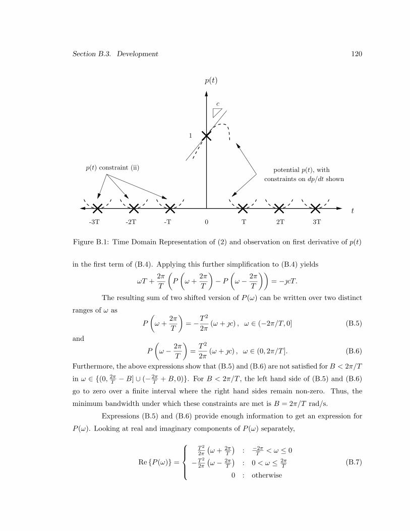
Section B.3. Development 120
p(t)
t
1
c
p(t) constraint (ii)
constraints on dp/dt shown
3T2TT0-T-2T-3T
potential p(t), with
Figure B.1: Time Domain Representation of (2) and observation on first derivative of p(t)
in the first term of (B.4). Applying this further simplification to (B.4) yields
ωT +2π
T
(P
(ω +
2π
T
)− P
(ω − 2π
T
))= −cT.
The resulting sum of two shifted version of P (ω) can be written over two distinct
ranges of ω as
P
(ω +
2π
T
)= −T 2
2π(ω + c) , ω ∈ (−2π/T, 0] (B.5)
and
P
(ω − 2π
T
)=
T 2
2π(ω + c) , ω ∈ (0, 2π/T ]. (B.6)
Furthermore, the above expressions show that (B.5) and (B.6) are not satisfied for B < 2π/T
in ω ∈ (0, 2πT − B] ∪ (−2π
T + B, 0). For B < 2π/T , the left hand side of (B.5) and (B.6)
go to zero over a finite interval where the right hand sides remain non-zero. Thus, the
minimum bandwidth under which these constraints are met is B = 2π/T rad/s.
Expressions (B.5) and (B.6) provide enough information to get an expression for
P (ω). Looking at real and imaginary components of P (ω) separately,
Re P (ω) =
T 2
2π
(ω + 2π
T
): −2π
T < ω ≤ 0
−T 2
2π
(ω − 2π
T
): 0 < ω ≤ 2π
T
0 : otherwise
(B.7)
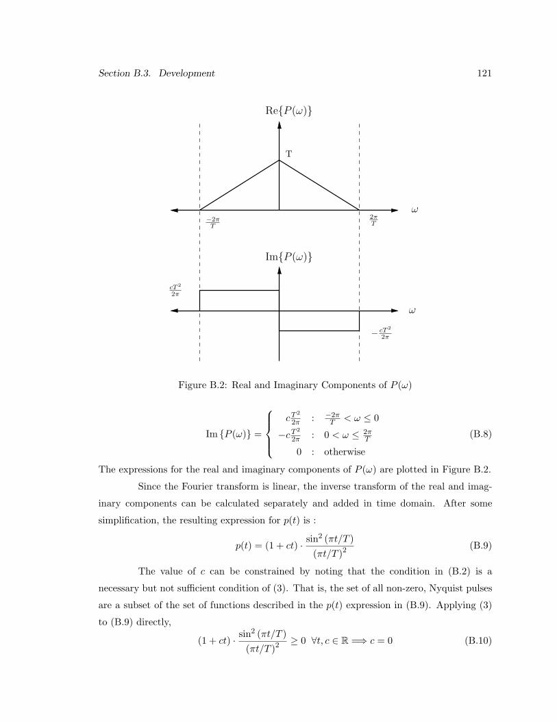
Section B.3. Development 121
ImP (ω)
ω
ω
T
ReP (ω)
−2πT
2πT
cT 2
2π
− cT 2
2π
Figure B.2: Real and Imaginary Components of P (ω)
Im P (ω) =
cT 2
2π : −2πT < ω ≤ 0
−cT 2
2π : 0 < ω ≤ 2πT
0 : otherwise
(B.8)
The expressions for the real and imaginary components of P (ω) are plotted in Figure B.2.
Since the Fourier transform is linear, the inverse transform of the real and imag-
inary components can be calculated separately and added in time domain. After some
simplification, the resulting expression for p(t) is :
p(t) = (1 + ct) · sin2 (πt/T )(πt/T )2
(B.9)
The value of c can be constrained by noting that the condition in (B.2) is a
necessary but not sufficient condition of (3). That is, the set of all non-zero, Nyquist pulses
are a subset of the set of functions described in the p(t) expression in (B.9). Applying (3)
to (B.9) directly,
(1 + ct) · sin2 (πt/T )(πt/T )2
≥ 0 ∀t, c ∈ R =⇒ c = 0 (B.10)

Section B.3. Development 122
Therefore, the minimum bandwidth Nyquist pulse which remains non-negative
occupies a bandwidth of 2π/T rad/s and takes the form :
p(t) =sin2 (πt/T )
(πt/T )2(B.11)
2

Bibliography
[1] Infrared Data Association, “Infrared data association serial infrared physical layer
specification,” Version 1.3, www.irda.org, 1998.
[2] International Electrotechnical Commission, “Safety of laser products – part 1: Equip-
ment classification, requirements and user’s guide,” Group safety publication, reference
number 825-1, 1993.
[3] D. J. T. Heatley, D. R. Wisely, I. Neild, and P. Cochrane, “Optical wireless: The story
so far,” IEEE Communications Magazine, pp. 72–82, December 1998.
[4] J. M. Kahn and J. R. Barry, “Wireless infrared communications,” Proceedings of the
IEEE, vol. 85, no. 2, pp. 263–298, February 1997.
[5] D. R. Goff, Fiber Optic Reference Guide — A Practical Guide to the Technology, Focal
Press, Boston, MA, 1996.
[6] D. P. Schinke, R. G. Smith, and A. R. Hartman, “Photodetectors,” in Semiconductor
Devices for Optical Communication, H. Kressel, Ed., chapter 3, pp. 61–87. Springer-
Verlag, Berlin, Germany, 1980.
[7] D. H. Navon, Semiconductor Microdevices and Materials, Holt, Rinehart and Winston,
New York, NY, 1986.
[8] M. Fukuda, Reliability and Degradation of Semiconductor Lasers and LEDs, Artech
House, Boston, MA, 1991.
[9] W. B. Leigh, Devices for Optoelectronics, Marcel Dekker, Inc., New York, NY, 1996.
123
Bibliography 124
[10] H. Kressel, M. Ettenberg, J. P. Wittke, and I. Ladany, “Laser diodes and LEDs for
fiber optical communication,” in Semiconductor Devices for Optical Communication,
H. Kressel, Ed., chapter 2, pp. 9–62. Springer-Verlag, Berlin, Germany, 1980.
[11] Siemens Microelectronics, “General IR and photodetector information,” Application
note 37, www.infineon.com/products/37/37.html, 1997.
[12] H. Melchior, M. B. Fisher, and F. R. Arams, “Photodetectors for optical communi-
cation systems,” Proceedings of the IEEE, vol. 58, no. 10, pp. 1466–1486, October
1970.
[13] S. Haykin, Digital Communications, John Wiley & Sons, New York, NY, 1988.
[14] R. Boyd-Merritt, “Blue Tooth group readies short-range RF LAN,” EE Times web
site, www.eet.com, May 14, 1998.
[15] Infrared Data Association, Web Site, www.irda.org.
[16] K. Lewotsky, Ed., “IR data link market to pass $290 million by 2002,” Photonics
Online web site, www.photonicsonline.com, September 23, 1998.
[17] Infineon Technologies, Inc., Web Site, www.infineon.com/irdt.
[18] IBM Electronics, Web Site, www.chips.ibm.com/products/infrared.
[19] JVC, VIPSLAN-10, Web Site, www.jvc-victor.co.jp/english/pro/lan-e/index.html.
[20] Spectrix Corporation, Web Site, www.spectrixcorp.com.
[21] CableFree Solutions Ltd., Web Site, www.cablefree.co.uk.
[22] P. L. Eardley and D. R. Wisely, “1Gbit/s optical free space link operating over 40m
– system and applications,” IEE Proceedings on Optoelectronics, vol. 143, no. 6, pp.
330–333, December 1996.
[23] J. R. Barry, Wireless Infrared Communications, Kluwer Academic Publishers, Boston,
MA, 1994.
[24] F. R. Gfeller and U. Bapst, “Wireless in-house communication via diffuse infrared
radiation,” Proceedings of the IEEE, vol. 67, no. 11, pp. 1474–1486, November 1979.
Bibliography 125
[25] J. M. Kahn, W. J. Krause, and J. B. Carruthers, “Experimental characterization of
non-directed indoor infrared channels,” IEEE Transactions on Communications, vol.
43, no. 2/3/4, pp. 1613–1623, February/March/April 1995.
[26] J. B. Carruthers and J. M. Kahn, “Modeling of nondirected wireless infrared channels,”
IEEE Transactions on Communications, vol. 45, no. 10, pp. 1260–1268, October 1997.
[27] J. Straus, “Linearized transmitters for analog fiber links,” Laser Focus, pp. 54–61,
October 1978.
[28] D. Hassin and R. Vahldieck, “Feedforward linearization of analog modulated laser
diodes–theoretcial analysis and experimental verification,” IEEE Transactions on Mi-
crowave Theory and Techniques, vol. 41, no. 12, pp. 2376–2382, December 1993.
[29] M. Bertelsmeier and W. Zschunke, “Linearization of broadband optical transmission
systems by adaptive predistortion,” Frequenz, vol. 38, no. 9, pp. 206–212, 1984.
[30] R. P. Feynman, R. B. Leighton, and M. Sands, The Feynman Lectures on Physics :
Vol I, Addson-Wesley Publishing, Reading, MA, 1977.
[31] Analog Devices Inc., “AD9660 laser diode driver with light power control,” Data sheet,
One Technology Way, Norwood, MA, 1995.
[32] P. W. Shumate and M. DiDomenico Jr., “Lightwave transmitters,” in Semiconductor
Devices for Optical Communication, H. Kressel, Ed., chapter 5, pp. 161–200. Springer-
Verlag, Berlin, Germany, 1980.
[33] S. B. Alexander, Optical Communication Receiver Design, Institution of Electrical
Engineers, SPIE Optical Engineering Press, London, UK, 1997.
[34] R. R. Hayes and D. L. Persechini, “Nonlinearity of p-i-n photodetectors,” IEEE
Photonics Technology Letters, vol. 5, no. 1, pp. 70–72, January 1993.
[35] R. G. Smith and S. D. Personick, “Receiver design for optical fiber communication
systems,” in Semiconductor Devices for Optical Communication, H. Kressel, Ed., chap-
ter 4, pp. 89–160. Springer-Verlag, Berlin, Germany, 1980.

Bibliography 126
[36] B. Zand, K. Phang, and D. A. Johns, “Transimpedance amplifier with differential pho-
todiode current sensing,” in IEEE International Symposium on Circuits and Systems,
1999, vol. II, pp. 624–627.
[37] K. Phang and D. A. Johns, “A 3-V CMOS optical preamplifier with dc photocurrent
rejection,” in IEEE International Symposium on Circuits and Systems, 1998, vol.
TAA8-8.
[38] ABB HAFO, “1A301 — high performance LED,” Data sheet, Mitel Microelectronics,
1994.
[39] Temic, “BPV 10 NF — high speed silicon pin photodiode,” Data sheet, Telefunken
Semiconductors, 1994.
[40] S. Karp, E. L. O’Neill, and R. M. Gagliardi, “Communication theory for the free-space
optical channel,” Proceedings of the IEEE, vol. 58, no. 10, pp. 1611–1626, October
1970.
[41] E. A. Lee and D. G. Messerschmitt, Digital Communication, Kluwer Academic Pub-
lishers, Boston, MA, second edition, 1994.
[42] R. Narasimhan, M. D. Audeh, and J. M. Kahn, “Effect of electronic-balast fluorescent
lighting on wireless infrared links,” IEE Proceedings on Optoelectronics, vol. 143 6, pp.
347–354, December 1996.
[43] H. Park and J. R. Barry, “Modulation analysis for wireless infrared communications,”
in IEEE International Conference on Communications, 1995, pp. 1182–1186.
[44] G. D. Forney Jr. and L.-F. Wei, “Multidimensional constellations – Part I: Introduction,
figures of merit, and generalized cross constellations,” IEEE Journal on Selected Areas
of Communications, vol. 7, no. 6, pp. 877–892, August 1989.
[45] F. R. Kschischang and S. Pasupathy, “Optimal nonuniform signalling for Gaussian
channels,” IEEE Transactions on Information Theory, vol. 39, no. 3, pp. 913–929,
May 1993.
[46] S. G. Wilson, Digital Modulation and Coding, Prentice-Hall, Upper Saddle River, NJ,
1996.
Bibliography 127
[47] S. Pasupathy, “ECE 1520S–Data Communications I Course Notes,” Course notes,
University of Toronto, 1998.
[48] J. G. Proakis, Digital Communications, McGraw-Hill, New York, NY, 1983.
[49] B. Reiffen and H. Sherman, “An optimum demodulator for Poisson processes: Photon
source detectors,” Proceedings of the IEEE, vol. 51, pp. 1316–1320, October 1963.
[50] K. Abend, “Optimum photon detection,” IEEE Transactions on Information Theory,
vol. 12, no. 1, pp. 64–65, January 1966.
[51] R. M. Gagliardi and S. Karp, “M-ary Poisson detection and optical communications,”
IEEE Transactions on Communication Technology, vol. COM-17, no. 2, pp. 208–216,
April 1969.
[52] S. Hranilovic and D. A. Johns, “A multilevel modulation scheme for high-speed wireless
infrared communications,” in IEEE International Symposium on Circuits and Systems,
1999, vol. VI, pp. 338–341.
[53] J. H. Conway and N. J. A. Sloane, Sphere Packings, Lattices and Groups, Springer-
Verlag, New York, NY, 2nd edition, 1993.
[54] G. D. Forney Jr., R. G. Gallager, G. R. Lang, F. M Longstaff, and S. U. Qureshi,
“Efficient modulation for band-limited channels,” IEEE Journal on Selected Areas in
Communications, vol. SAC-2, no. 5, pp. 632–647, September 1984.
[55] D. Lind and B. Marcus, An Introduction to Symbolic Dynamics and Coding, Cambridge
University Press, New York, NY, 1995.
[56] K. A. Schouhamer Immink, Coding Techniques for Digital Recorders, Prentice-Hall
International, London, UK, 1991.
[57] R. Karabed and B. H. Marcus, “Sliding-block coding for input-restricted channels,”
IEEE Transactions on Information Theory, vol. 34, no. 1, pp. 2–26, January 1988.
[58] C. E. Shannon, “A mathematical theory of communication,” Bell System Technical
Journal, vol. 27, pp. 379–423, 623–656, July, October 1948.

Bibliography 128
[59] R. L. Adler, D. Coppersmith, and M. Hassner, “Algorithms for sliding block codes –
an application of symbolic dynamics to information theory,” IEEE Transactions on
Information Theory, vol. IT-29, no. 1, pp. 5–22, January 1983.
[60] B. Marcus, “Sofic systems and encoding data,” IEEE Transactions on Information
Theory, vol. IT-31, no. 3, pp. 366–377, May 1985.
Top Related