


Languages
Pages
Legal


MICROMACHINED THIN-FILM SENSORS FOR SOI-CMOS CO-INTEGRATION

Micromachined Thin-Film Sensorsfor SOI-CMOS Co-Integration
Dr. J. LACONTEIntersema Sensoric SA, Bevaix, Switzerland
Prof. D. FLANDREUniversité Catholique de Louvain,
and
Prof. J.-P. RASKINUniversité Catholique de Louvain,Louvain-La-
by
Louvain-La-Neu e, Belgiumv
Neu e, Belgiumv
A C.I.P. Catalogue record for this book is available from the Library of Congress.
ISBN-10 0-387-28842-2 (HB)ISBN-13 978-0-387-28842-0 (HB)
ISBN-13 978-0-387-28843-7 (e-book)
Published by Springer,P.O. Box 17, 3300 AA Dordrecht, The Netherlands.
Printed on acid-free paper
All Rights Reserved
No part of this work may be reproduced, stored in a retrieval system, or transmittedin any form or by any means, electronic, mechanical, photocopying, microfilming, recordingor otherwise, without written permission from the Publisher, with the exceptionof any material supplied specifically for the purpose of being enteredand executed on a computer system, for exclusive use by the purchaser of the work.
Printed in the Netherlands.
ISBN-10 0-387-28843-0 (e-book)
www.springer.com
© 2006 Springer

Abstract
While in some applications such as gas-flow sensors, the co-integration of a sensor with
its surrounding electronics on a single chip is just an asset, co-integration is inescapable
in other cases such as transistors-based pressure sensors or low-loss microwave circuits
insulated from the substrate, on a membrane. Moreover, co-integration performed in the
most advanced of the Complementary-Metal-Oxide-Semiconductor (CMOS) technologies
to date -namely Silicon-on-Insulator (SOI) technology- provides many significant benefits
regarding the performance, reliability, miniaturization and processing easiness without
significantly increasing the final cost.
Thin dielectric membranes constitute the starting material for a large number of sen-
sors thanks to their ability to act as a mechanical support or an electrical and thermal
insulator. We particularly focused on the thermal insulation feature to build fully CMOS-
SOI co-integrated gas-flow sensors. A one-µm-thick robust and flat dielectric multilayered
membrane has been built taking precisely into account the residual stresses in each consti-
tutive layer. A complete review and summary of the main concepts of thin film mechanics
is detailed for an in-depth understanding. A new measurement methodology based on
substrate curvature and deflected microstructures has been developed in order to accu-
rately quantify the residual stresses in each layer and in their stacking. To release the
membrane in post-processing, the Tetramethyl Ammonium Hydroxide (TMAH) silicon
micromachining solution has been used and optimized in order to increase its selectivity
towards aluminum. This particular wet etching technique was extensively reviewed and
enhanced by our own experiments, in particular for assuring CMOS compatibility.
A novel loop-shape polysilicon microheater implementing the basic heating cell of new
simple gas-flow sensors has been designed and produced in a CMOS-SOI standard process.
High thermal uniformity, low power consumption and high working temperature have been
targeted and confirmed by extensive measurements. In particular, the electrical properties
of polysilicon versus temperature and annealing time have been analyzed in depth. The
gas-flow sensor has been optimized to be integrated in intermediate- and post-processing
v

of a standard CMOS-SOI fabrication. The thermopiles of the flow sensor as well as the
interdigitated electrodes of the gas sensor have judiciously been chosen in this purpose.
The sensing films of the gas sensors consisted in sputtered and drop coated metal oxide
layers such as SnO2 and WO3. Measurements in the presence of a nitrogen flow and gas
revealed a fair sensitivity on a large flow velocity range for the flow transducer, as well
as a good sensitivity to gases such as ethanol, ammonia and nitrogen dioxide for the gas
transducer. The whole process has confirmed its full CMOS compatibility by measuring
MOS transistors, capacitors and gated diodes on the same chip as the sensors after each
post-processing step.
Finally, transistors integrated in small silicon islands located in the middle of our
dielectric membrane have been studied and presented as a concluding demonstrator of
the co-integration in SOI technology. Such devices open the door to numerous new ap-
plications where integrated circuits and sensors are merged in order to target higher
vi
performance in harsh environments.

Acknowledgments
The authors are grateful to the external members of Mr. Laconte’s PhD jury, Professors
Dominique Collard, Eduard Llobet and Nico de Rooij who gave judicious advices to put
the final touch to the researches and the manuscript.
Large parts of the work presented in this book are the result of collaborations with the
technical staff of UCL clean-rooms. We would really like to thank Andre Crahay, Christian
Renaux, David Spote, Nathanael Mahieux for their devotedly help for processing the
unrewarding steps of the fabrications, without forgetting Bohdan Katschmarskyj for its
occasional implantations. Pierrot Loumaye and Miloud Zitout were also of great help
to perform the incalculable wafer dicing and sensors packaging. We would also like to
thank Laurent Morelle and Miloud Zitout for their electrical realizations as well as Pierrot
Loumaye for his numerous mechanical manufacturings.
The students supported during their master theses were also essential to the accom-
plishment of this work. We would like to thank Cedric Dupont, Valerie Wilmart and
Bertrand Rue. The help of Sebastien Jorez from the optical Laboratory of the university
was also invaluable to me. He devoted a large part of its post-doctoral research to per-
form all the needed optical measurement set-ups, with a great patience and always, with
a lot of efficiency. Thomas Pardoen, Yannick Bertholet and Joris Proost from the IMAP
laboratory of the university were also of great help for their numerous advices in the me-
chanics of materials. Peter Tsolov Ivanov, thank you for your gas sensors measurements
in Tarragona. We would also thank other UCL researchers, especially Bertrand Parvais,
Francois Iker, Remi Charavel, Luis Moreno, Remi Pampin, David Levacq, Andre Tuor,
Loık Gence, Aryan Afzalian, Valeria Kilchytska and Alexandru Vlad who collaborated in
the fabrications, designs or even in the reading of some parts of this manuscript. Many
thanks for your pleasant company.
We also thank the computing staff of our laboratory which solved the incredible num-
ber of little problems I faced on Windows or Unix environments, Brigitte Dupont, Geoffroy
vii

Simon, Damien Giry and Laurent Vancaillie. Moreover, we cannot thank enough our sec-
retaries, Anne Adant and Annette Kreuwels and our accountant, Marie-Helene Dewael
for the numerous urgent orders, always placed at the last minute.
Our final thoughts go to Axelle for her help to correct the introduction and conclusions
of this work. Jean also especially thanks his wife, Benedicte, who immensely supported
him in his daily investments for his thesis and who encouraged him to finalize it despite
of the organization of their wedding at the same time...
Denis and Jean-Pierre have also grateful thoughts for their wives and children who
sometimes endure their long working hours and regular absences.
viii

Contents
I Introduction: Context and motivations 1
0.1 Why Silicon-on-Insulator technology ? . . . . . . . . . . . . . . . . . . . . 4
0.2 Why a thin-film membrane ? . . . . . . . . . . . . . . . . . . . . . . . . . . 6
0.3 Why co-integration and CMOS compatibility ? . . . . . . . . . . . . . . . . 8
0.4 Contents of the work . . . . . . . . . . . . . . . . . . . . . . . . . . . . . . 10
II Techniques and materials 15
1 Silicon bulk micromachining with TMAH 17
1.1 Introduction . . . . . . . . . . . . . . . . . . . . . . . . . . . . . . . . . . . 17
1.2 Generalities about silicon micromachining . . . . . . . . . . . . . . . . . . 19
1.3 TMAH silicon etching . . . . . . . . . . . . . . . . . . . . . . . . . . . . . 23
1.4 Selectivity versus dielectrics . . . . . . . . . . . . . . . . . . . . . . . . . . 28
1.5 Selectivity versus aluminum . . . . . . . . . . . . . . . . . . . . . . . . . . 29
1.5.1 State of the art . . . . . . . . . . . . . . . . . . . . . . . . . . . . . 29
1.5.2 Experimental results . . . . . . . . . . . . . . . . . . . . . . . . . . 32
1.5.3 Summary of the TMAH etching steps in presence of Al . . . . . . . 36
1.6 Selectivity versus other metals . . . . . . . . . . . . . . . . . . . . . . . . . 37
1.7 Etch-Stop . . . . . . . . . . . . . . . . . . . . . . . . . . . . . . . . . . . . 38
1.8 Undercutting . . . . . . . . . . . . . . . . . . . . . . . . . . . . . . . . . . 41
1.8.1 Generalities . . . . . . . . . . . . . . . . . . . . . . . . . . . . . . . 41
1.8.2 Membranes patterning . . . . . . . . . . . . . . . . . . . . . . . . . 43
1.9 Summary . . . . . . . . . . . . . . . . . . . . . . . . . . . . . . . . . . . . 45
2 Thin dielectric films stress extraction 47
2.1 Introduction - Definitions . . . . . . . . . . . . . . . . . . . . . . . . . . . 48
2.1.1 Stress, strain and Elastic constants . . . . . . . . . . . . . . . . . . 48
2.1.2 Uniform and non-uniform stresses and strains in thin films . . . . . 52
ix

CONTENTS
Extrinsic stress . . . . . . . . . . . . . . . . . . . . . . . . . . . . . 53
Intrinsic stress . . . . . . . . . . . . . . . . . . . . . . . . . . . . . . 55
2.2 Stress measurements by substrate
curvature method . . . . . . . . . . . . . . . . . . . . . . . . . . . . . . . . 56
2.2.1 Theory . . . . . . . . . . . . . . . . . . . . . . . . . . . . . . . . . . 56
2.2.2 Experimental results . . . . . . . . . . . . . . . . . . . . . . . . . . 61
2.2.3 Discussions and summary . . . . . . . . . . . . . . . . . . . . . . . 68
2.3 Strain measurements using micromachined
structures . . . . . . . . . . . . . . . . . . . . . . . . . . . . . . . . . . . . 69
2.3.1 Clamped-clamped beam and ring-and-beam
structures analysis . . . . . . . . . . . . . . . . . . . . . . . . . . . 71
Theory . . . . . . . . . . . . . . . . . . . . . . . . . . . . . . . . . . 71
Experimental setups and results . . . . . . . . . . . . . . . . . . . . 76
2.3.2 Microgauges analysis . . . . . . . . . . . . . . . . . . . . . . . . . . 82
2.3.3 Cantilever beams analysis . . . . . . . . . . . . . . . . . . . . . . . 86
Monolayer cantilever beams . . . . . . . . . . . . . . . . . . . . . . 86
Multilayer cantilever beams . . . . . . . . . . . . . . . . . . . . . . 94
Discussion on multilayer membranes . . . . . . . . . . . . . . . . . 96
2.3.4 Summary and outlook . . . . . . . . . . . . . . . . . . . . . . . . . 97
2.4 Final conclusions . . . . . . . . . . . . . . . . . . . . . . . . . . . . . . . . 102
III Microsensors 105
1 Low power microhotplate as basic cell 107
1.1 Introduction . . . . . . . . . . . . . . . . . . . . . . . . . . . . . . . . . . . 107
1.2 Motivations . . . . . . . . . . . . . . . . . . . . . . . . . . . . . . . . . . . 110
1.2.1 Gas sensors . . . . . . . . . . . . . . . . . . . . . . . . . . . . . . . 110
1.2.2 Other sensors . . . . . . . . . . . . . . . . . . . . . . . . . . . . . . 111
1.3 Materials selection . . . . . . . . . . . . . . . . . . . . . . . . . . . . . . . 111
1.3.1 Membrane . . . . . . . . . . . . . . . . . . . . . . . . . . . . . . . . 111
1.3.2 Microheater . . . . . . . . . . . . . . . . . . . . . . . . . . . . . . . 112
1.4 Thermal design . . . . . . . . . . . . . . . . . . . . . . . . . . . . . . . . . 113
1.4.1 Basis of heat transfer theory . . . . . . . . . . . . . . . . . . . . . . 113
Conduction . . . . . . . . . . . . . . . . . . . . . . . . . . . . . . . 113
Convection . . . . . . . . . . . . . . . . . . . . . . . . . . . . . . . 114
Radiation . . . . . . . . . . . . . . . . . . . . . . . . . . . . . . . . 115
x

CONTENTS
1.4.2 Thermal simulations . . . . . . . . . . . . . . . . . . . . . . . . . . 115
1.5 Device fabrication . . . . . . . . . . . . . . . . . . . . . . . . . . . . . . . . 120
1.5.1 On bulk silicon substrate . . . . . . . . . . . . . . . . . . . . . . . . 120
1.5.2 On SOI substrate . . . . . . . . . . . . . . . . . . . . . . . . . . . . 122
1.5.3 Dicing and packaging . . . . . . . . . . . . . . . . . . . . . . . . . . 126
1.6 Microheater characterization and results . . . . . . . . . . . . . . . . . . . 127
1.6.1 Introduction . . . . . . . . . . . . . . . . . . . . . . . . . . . . . . . 127
1.6.2 Calibrations . . . . . . . . . . . . . . . . . . . . . . . . . . . . . . . 129
1.6.3 Measurements . . . . . . . . . . . . . . . . . . . . . . . . . . . . . . 133
1.6.4 Discussion on the microheater geometry . . . . . . . . . . . . . . . 136
1.6.5 Thermal uniformity measurements . . . . . . . . . . . . . . . . . . 138
1.6.6 Measurements at high temperatures . . . . . . . . . . . . . . . . . . 142
Experimental results . . . . . . . . . . . . . . . . . . . . . . . . . . 142
Physical and structural behavior . . . . . . . . . . . . . . . . . . . . 148
Summary . . . . . . . . . . . . . . . . . . . . . . . . . . . . . . . . 149
1.6.7 Thermal ageing . . . . . . . . . . . . . . . . . . . . . . . . . . . . . 150
Tests at constant current . . . . . . . . . . . . . . . . . . . . . . . . 150
Tests at constant voltage . . . . . . . . . . . . . . . . . . . . . . . . 153
Physical explanations . . . . . . . . . . . . . . . . . . . . . . . . . . 156
Summary . . . . . . . . . . . . . . . . . . . . . . . . . . . . . . . . 157
1.6.8 Reliability . . . . . . . . . . . . . . . . . . . . . . . . . . . . . . . . 158
1.7 Conclusions . . . . . . . . . . . . . . . . . . . . . . . . . . . . . . . . . . . 159
2 Microheater based flow sensor 163
2.1 Introduction . . . . . . . . . . . . . . . . . . . . . . . . . . . . . . . . . . . 163
2.2 Design and fabrication . . . . . . . . . . . . . . . . . . . . . . . . . . . . . 164
2.3 Measurements results . . . . . . . . . . . . . . . . . . . . . . . . . . . . . . 168
2.3.1 Calibration and temperature measurements without flow . . . . . . 168
2.3.2 Microheater and thermopiles response time measurements without
flow . . . . . . . . . . . . . . . . . . . . . . . . . . . . . . . . . . . 173
2.3.3 Flow measurements . . . . . . . . . . . . . . . . . . . . . . . . . . . 175
Introduction . . . . . . . . . . . . . . . . . . . . . . . . . . . . . . . 175
Sensor in configuration 1 . . . . . . . . . . . . . . . . . . . . . . . . 176
Sensor in configuration 2 . . . . . . . . . . . . . . . . . . . . . . . . 179
Sensor in configuration 3 . . . . . . . . . . . . . . . . . . . . . . . . 184
Discussions and summary . . . . . . . . . . . . . . . . . . . . . . . 185
xi

CONTENTS
2.4 Discussions and comparison with the
state-of-the-art . . . . . . . . . . . . . . . . . . . . . . . . . . . . . . . . . 187
2.5 Conclusions . . . . . . . . . . . . . . . . . . . . . . . . . . . . . . . . . . . 188
3 Gas Sensors on microhotplate 193
3.1 Introduction . . . . . . . . . . . . . . . . . . . . . . . . . . . . . . . . . . . 193
3.2 Interdigitated electrodes: from design
to deposition . . . . . . . . . . . . . . . . . . . . . . . . . . . . . . . . . . 195
3.2.1 Design . . . . . . . . . . . . . . . . . . . . . . . . . . . . . . . . . . 195
3.2.2 Metal selection and deposition . . . . . . . . . . . . . . . . . . . . . 196
3.3 Sensitive layer deposition . . . . . . . . . . . . . . . . . . . . . . . . . . . . 200
3.4 Summary of the fabrication steps . . . . . . . . . . . . . . . . . . . . . . . 203
3.5 Measurements results without gas . . . . . . . . . . . . . . . . . . . . . . . 205
3.6 Measurement results under gas and discussions . . . . . . . . . . . . . . . . 207
3.7 Conclusions . . . . . . . . . . . . . . . . . . . . . . . . . . . . . . . . . . . 212
4 SOI-CMOS compatibility validation 213
4.1 Introduction . . . . . . . . . . . . . . . . . . . . . . . . . . . . . . . . . . . 213
4.2 Basics of SOI technology . . . . . . . . . . . . . . . . . . . . . . . . . . . . 215
4.2.1 The main SOI technology issues . . . . . . . . . . . . . . . . . . . . 216
4.2.2 The transconductance over drain ratio current . . . . . . . . . . . . 218
4.2.3 The properties of the oxide and the Si/SiO2 interface traps . . . . . 218
4.3 Post-processing steps . . . . . . . . . . . . . . . . . . . . . . . . . . . . . . 220
4.4 Measurements . . . . . . . . . . . . . . . . . . . . . . . . . . . . . . . . . . 220
4.4.1 MOS transistors . . . . . . . . . . . . . . . . . . . . . . . . . . . . . 222
Measurements results . . . . . . . . . . . . . . . . . . . . . . . . . . 222
Discussion . . . . . . . . . . . . . . . . . . . . . . . . . . . . . . . . 225
4.4.2 MOS capacitors . . . . . . . . . . . . . . . . . . . . . . . . . . . . . 230
4.4.3 Gated Diodes . . . . . . . . . . . . . . . . . . . . . . . . . . . . . . 232
4.4.4 Summary . . . . . . . . . . . . . . . . . . . . . . . . . . . . . . . . 234
4.5 Transistors on membrane as final demonstrator . . . . . . . . . . . . . . . 235
4.5.1 Design and fabrication . . . . . . . . . . . . . . . . . . . . . . . . . 235
4.5.2 Measurements and discussion . . . . . . . . . . . . . . . . . . . . . 238
4.5.3 Applications . . . . . . . . . . . . . . . . . . . . . . . . . . . . . . . 241
Pressure sensor . . . . . . . . . . . . . . . . . . . . . . . . . . . . . 241
Gas sensor . . . . . . . . . . . . . . . . . . . . . . . . . . . . . . . . 242
xii
CONTENTS
4.6 Conclusions . . . . . . . . . . . . . . . . . . . . . . . . . . . . . . . . . . . 243
IV Conclusions and outlook 245
Appendixes 253
A (100) Silicon crystallography 255
B About Interferometry... 259
C About Reflectometry... 263
Bibliography 265
Publications originated from this work 285
Index 289
xiii

Part I
Introduction: Context and
motivations

3
Sensors are devices that provide an interface between the electronics and the physical
world. When converting non-electrical physical or chemical quantities into electrical sig-
nals, the sensors help the electronics to “see”, “hear”, “smell”, “taste”, and “touch” [1].
Sensors have become an essential element of process control and measurement systems
in almost all spheres of our life and tend to be more and more miniaturized. Electrical
signals coming from sensors always need to be processed in order to be understood by the
sensor user, and require therefore additional electronics. Unfortunately, sensor fabrica-
tion techniques (such as micromachining) are only more or less compatible with electronic
circuits which are processed using the well established Complementary Metal Oxide Semi-
conductor (CMOS) process. These circuits can then be placed far away from the sensor
and its environment to sense, and can be connected to the sensor by wires of which the
length can vary. Sensor and electronics can also be implemented on two different chips
connected together with thin wires in the same package, and placed in the environment
to sense. In both cases, electronics and sensors are separately processed and connected
together at the end of the process so as to avoid compatibility problems during their
fabrication. Such solutions are named hybrid solutions since they use microelectronics
fabrication techniques but cannot be merged due to some incompatibilities. Most of the
high production sensors -such as pressure sensors and accelerometers- which we can find
in the automotive sector, are processed this way thanks to their lower cost (less processing
steps).
Nevertheless, in order to shrink their size, to increase their performances, their reli-
ability and their economical added value, it intuitively seems more efficient to integrate
the sensor and its electronics on the same silicon die. This technique is thus called co-
integration and the resulting co-integrated device is called smart sensor or microsystem.
In such fabrication processes, the compatibility between CMOS techniques and the ones
that are necessary to build sensors must be complete.

4 Introduction: Context and motivations
The purpose of this work, by means of typical sensors realizations, is to add contri-
butions to the growing research in this promising field (see more particularly the works
of Baltes and its staff, in [2]). We will especially focus on a specific process technology,
Silicon-on-Insulator (SOI), which is the best candidate for successful co-integrations in
the largest kinds of applications. Only sensors based on micromachined thin film
membranes will be studied, especially thermal sensors which need to be built on dielec-
tric membranes to ensure a maximal thermal insulation and maintain power as low as
possible.
In this introductive part, we firstly justify our choice regarding the fact that all this
work is based on SOI technology. We explain then why thin film membranes are essential
to successfully sense the surrounding world as well as to increase the performance of
some integrated circuits. A debate follows about the advantages and drawbacks of the
co-integration on the same chip. Finally, the table of contents is detailed.
0.1 Why Silicon-on-Insulator technology ?
Silicon-on-Insulator (SOI) technology is the most advanced of the present CMOS tech-
nologies [3]. This technology offers the possibility of building electronic devices on a thin
layer of silicon that is electrically isulated from the thick silicon substrate through the
use of a buried dielectric layer. In standard silicon technology (named bulk Si), the sili-
con substrate is associated with undesirable effects such as high leakage currents from the
source and drain towards the substrate, parasitic bipolar components, parasitic source and
drain capacitances and more importantly, interference between individual active devices
or circuits built in the same integrated chip [3]. The use of Silicon-on-Insulator (SOI) sub-
strate is likely the best way to overcome the limitations of bulk technology. The insulating
layer blocks charge transport between the active layer and the substrate, featuring this
technology as the best one for radiation and high temperature environments, like outer
space [4][5], military or industrial, avionics and automotive sectors [6][7]. In addition,
the reduction of parasitic capacitances and leakage currents allow better high-frequency
performances and lower power consumption when compared to bulk counterparts [8]. Fi-
nally, SOI devices benefit from improved insulation between devices which allows higher
device density compared to that possible in bulk Si [4].
The first confirmation that SOI technology has become the state-of-the-art technology
in low power high speed ICs came when IBM announced its first fully functional SOI
0.1. WHY SILICON-ON-INSULATOR TECHNOLOGY ? 5
mainstream microprocessor in 1998. More recently, AMD started its new generation of
high-end microprocessors based on SOI technology. Nowadays, SOI ICs are only a fraction
more expensive than their counterparts made in bulk technology (10 or 15 % more per
die [4]). This is due to the high initial costs of the SOI wafers (3 or 4 times as much as
bulk silicon [4]). These are however counterbalanced by the reduction of process steps and
by the higher packing density of ICs per wafers. In addition, it is expected that as the
volume of SOI wafers increases, the costs will significantly decrease, i.e. making SOI the
favorite route to ultimate MOS devices [3][4].
Recently, SOI technology has also been applied to Micro-Electro-Mechanical Sensors
(MEMS) [9][10]. The buried oxide present in the SOI material can be very successfully
used as an etch-stop layer for both wet and dry bulk micromachinings, either from the back
or from the front side of the wafer. When releasing the silicon substrate from the backside
of the wafer for instance, a stacked buried-oxide/silicon membrane can be obtained. The
high quality of the top crystalline silicon film enables semiconductor devices such as
temperature sensors, microheaters, MOSFETs, microwave circuits to be built within the
membrane in order to get a better thermal or electrical insulation. This membrane can
also play the role of support for mechanical sensors to sense pressure for instance, and
integrate their sensing elements such as piezoresistors, directly in the silicon film. The
use of SOI material is imperative in the cases where a silicon membrane is desired.
The merit of silicon as a mechanical material in comparison to other ones do not need
to be reminded. The ability to use Si as a superficial layer for surface micromachined
structures is a great benefit and can be fulfilled by SOI technology. In this case, the surface
micromachining consists in selectively etching the buried oxide, acting as a sacrificial layer,
in order to release silicon structures in suspension above the substrate. The sacrificial layer
features in this case a high etching selectivity compared to the superficial layer and the
substrate (both silicon layers), and a high degree of uniformity. Capacitive structures
between the top silicon film and the substrate can be built this way [9].
The use of SOI thereby appears as the best approach for processing either circuits or
sensors. In addition, it offers the unique advantage to save a great deal of design time
and efforts in fabrication of microsystems, combining the electronics and the sensors on
the same chip, in order to improve their thermal, electrical and mechanical performances.
Furthermore, the high temperature and radiation hardness of SOI technology make it
the best option to achieve microsystems dedicated to work in harsh environment, such as
automotive, aerospace and military sectors.
6 Introduction: Context and motivations
0.2 Why a thin-film membrane ?
Our work especially focuses on sensors requiring a thin film dielectric membrane to achieve
a great thermal insulation coupled with a low electrical power consumption. It is well
known that silicon conducts heat very well (its thermal conductivity is about 100 times
higher than silicon oxide [11]) and therefore leads to consume a lot of power to reach a
temperature as high as 400◦C. Dielectric membranes, as thin as 1 µm, constitute thereby
the best choice for thermal insulation.
A dielectric membrane can also play two main other functions:
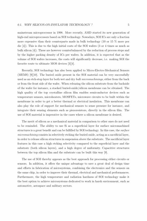
• A significant purpose of a dielectric membrane is its ability to provide with elec-
trical insulation. A typical application based on this purpose is demonstrated
when integrating a meander microwave inductor (Fig. 1(a)) on the membrane and
comparing its quality factor as well as its resonance frequency with and without the
silicon substrate. The results depicted in Fig. 1(b) show that the membrane enables
to increase the resonance frequency as well as the quality factor of the inductance
thanks to the loss of parasitic capacitances to the substrate. The same kinds of
results were reported in [12].
(a) (b)
Figure 1: (a) Picture of a meander inductor (0.65 nH) on our dielectric membrane; (b), qualityfactor Q versus frequency for the meander on membrane and on substrate.
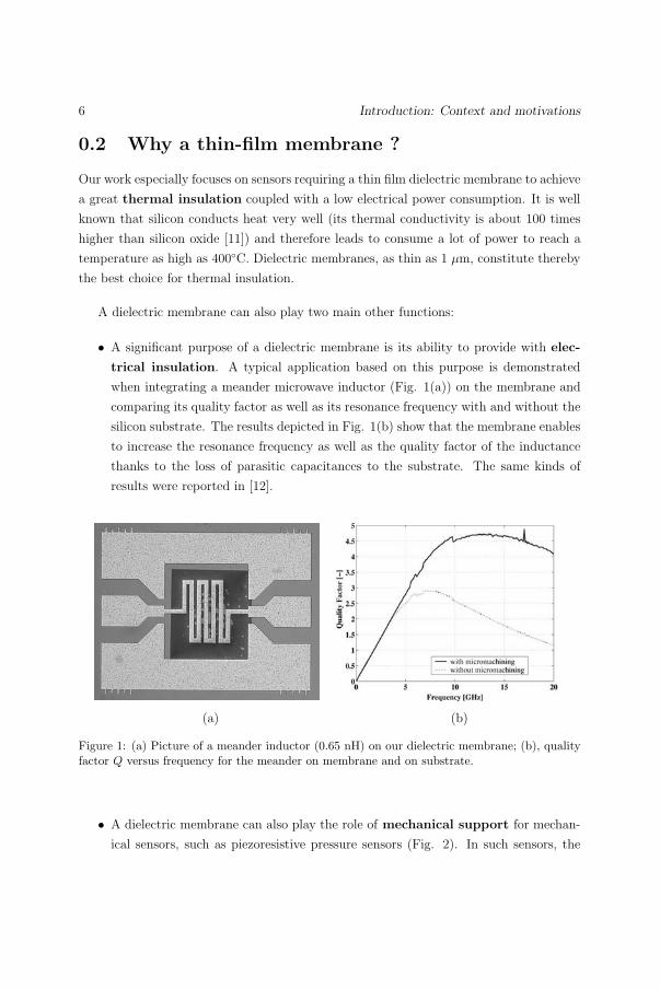
• A dielectric membrane can also play the role of mechanical support for mechan-
ical sensors, such as piezoresistive pressure sensors (Fig. 2). In such sensors, the
0.2. WHY A THIN-FILM MEMBRANE ? 7
membrane is deflected by a difference between the upper and lower applied pres-
sures. The membrane deformation induces a resistance variation in the 4 polysilicon
piezoresistors connected in a Wheatstone bridge, and then a voltage difference across
the bridge, that is proportional to the differential pressure which is applied [13].
Figure 2: Pressure sensor on dielectric membrane based on 4 polysilicon piezoresistors connectedin Wheatstone bridge.
It must be noted that in some cases, the dielectric membrane that is built from the
standard inorganic layers of the microelectronics fabrication can be successfully replaced
by an other constituting material, i.e. Polyimide for instance. This is a new promising
organic polymer, fully CMOS compatible, that features high dielectric properties, high
planarization, excellent self-adhesion, high thermal stability, ease of patterning (coat-
ing by centrifugation and photosensitive), great chemical stability and good mechanical
properties such as high elasticity and low thermal dilatation coefficient [14]. In addition,
it offers the great advantage to be deposited in much higher thickness compared to oxide
or nitride. Polyimide can be successfully used as an electrical insulator for high frequency
sensors as reported in [15], or as a thermal insulator for thermal sensors [16]. Further-
more, it can be noted that -thanks to its high water permeability in some formulas- it can
constitute the sensing layer of a humidity sensor [17].

8 Introduction: Context and motivations
0.3 Why co-integration and CMOS compatibility ?
In some applications, it can be sufficient to package the sensor and the signal-processing
electronics on two separate chips (or dies), but in a single module, using hybrid technolo-
gies [13]. Such technologies thereby require interconnection wires between the sensor-chip
and the electronic-chip, processed separately but finally integrated in the same package.
This technology allows for performing very low cost (but low performance) sensors on
their own chip, coupled with powerful electronics dedicated to offset their defects, on a
second chip in the same package. This technology is well established in many high pro-
ductivity sensors companies due to its low cost per chip since requiring less processing
steps.
On the other hand, the co-integration on the same chip, of the signal circuitry with
the sensor structure is determined mostly by how the performance, the reliability, the size
gain, the overall yield, the packaging and the overall system cost are affected. Neverthe-
less, in many applications, to reach high performances, co-integration nowadays appears
inescapable and can plentifully be justified by an eventually lower starting cost.
In the first example (electrical insulation) outlined here above, we showed that the bulk
micromachining, which is a typical sensor-fabrication technology, and passive microwave
circuits require to be intimately co-integrated to increase their frequency performance. In
addition, when the typical described inductor needs to be integrated into a more complex
circuit (in a high-frequency and low-power oscillator for instance), the hybrid technology
is unthinkable due to the too high parasitic capacitances between the interconnections
wires which would increase the response time, as well as the power consumption.
On the contrary, the pressure sensor of the second example does not need to be espe-
cially co-integrated with its electronics on the same chip to be impressive. Nevertheless,
polysilicon piezoresistors requiring a Wheatstone bridge to provide an interpretable sig-
nal, are more and more replaced by MOS transistors in order to make an easier signal
processing and to get an increase in the sensor sensitivity in some applications [18]. An
example will be discussed in the last chapter (last part). In this case, co-integration still
appears to be an asset.
Regarding gas sensors, solid state gas sensors of semiconductor type deposited on ce-
ramic substrates have been known for more than 25 years, but it is only recently that
the possibility of using microelectronics technology to fabricate them has been contem-
plated [19]. This technological revolution offers several advantages such as small size, low

0.3. WHY CO-INTEGRATION AND CMOS COMPATIBILITY ? 9
weight, low power consumption, more uniform temperature distribution, low cost due to
automatic and batch production [19] for this kind of sensors. The considerable interest
for such sensors arises from the need to find solutions everywhere -from the industrial,
agricultural and military activities to the domestic ones- to reinforce environmental reg-
ulations for the next decades [20], and fully justifies the growing research in this field. In
addition, the possibility to co-integrate the sensor and its electronics on the same chip
increases its fabrication easiness, especially in the SOI technology, as discussed above [3].
Consequently, such gas sensing microsystems can be used in radiation or high tempera-
ture environments, without affecting their reliability. It would not be the case if the same
sensor was integrated in hybrid technology.
Finally, the co-integration interest is to a large extent dependent on economic con-
siderations [13]. An important economic factor is the yield of both the sensor and the
circuitry. For most semiconductor sensors, it is expected that the yield will be dominated
by gross defects, or parametric processing problems (e.g. errors of proportions in the
preparation of a wet etchant), as opposed to the situation in integrated circuits where
random defects (e.g. pinholes, photolithographic defects) dominate the yield. This is due
to the difference of area between circuits and sensors, and their difference of physical and
structural complexity. The yield of integrated circuits is strongly dependent on the area of
the circuit. Therefore, while the circuit yield is determined especially by the circuit area
and the defect density, the overall yield of a co-integrated sensor-circuit chip will moreover
depend on the number of additional processing steps that have to be performed, which
results in its reduction [13].
An other important problem linked to sensors is their packaging. No sensor can be
designed without a consideration of the final package and the influence on its final costs
[13]. The package for each type of sensor is different and has different requirements as it
must transfer the variable being measured to the sensor while protecting the sensor from
harmful environmental effects [13].When sensors and circuits are co-integrated on the same
chip, the packaging becomes easier and cheaper to design and fabricate, especially thanks
to the reduction in the number of wire bonds. Consequently, the long-term reliability is
increased as well as the miniaturization.
In conclusion, in most cases, co-integration may increase the costs because of the ad-
ditional processing (and therefore decreased yield) and design efforts of the individual Si
devices. However, the manufacture final cost of a reliable system is not always increased.
Packaging problems are reduced, co-integration increases the long-term reliability as well

10 Introduction: Context and motivations
as the miniaturization and it can improve the overall system performance with less com-
ponents, which results in a higher quality system. Furthermore, if SOI technology is used,
the microsystem performances as well as its design easiness are increased, featuring finally
high performance sensors which often offset the higher costs of the starting SOI material.
0.4 Contents of the work
The content of the present work is divided in two main sections following the introductive
part I. Part II will focus on the techniques and materials, especially the TMAH silicon
bulk micromachining used to release our membranes and the measurements of the resid-
ual stresses in the thin dielectric films which will constitute our membrane. Part III will
describe our sensors realizations based on such thin dielectric micromachined membranes.
Two sensors will be investigated, both of them based on a unique basic cell, a microhot-
plate designed to uniformly heat a given area of the membrane. This last part will be
concluded by an in-depth study aimed at validating the fully SOI-CMOS compatibility
of our devices.
Chapter 1 of part II is focused on a particular silicon micromachining technique
based on the TetraMethyl Ammonium Hydroxide (TMAH) wet etchant dedicated to ma-
chine a dielectric membrane from the silicon substrate. This well-known technique has
been recently introduced in the world of MEMS. Tabata et all. [21] reported in 1992 their
first tests with this promising technique. This etchant featured the great advantage, in
comparison with former ones, to be fully CMOS compatible and easy to handle. The
amount of publications on this technique has slightly been increasing after ’92 with a first
significant peak around 1998. Nevertheless, a lot of review papers and books still reported
the same results. Nowadays, this technique is well documented but needs to be carefully
reviewed in order to be well defined. Our review on the TMAH etching is the first original
contribution of this work. All its etching properties are described and illustrated with
our own tests performed with our in-house optimized etching benches. The selectivity
of TMAH versus aluminum is especially studied and we develop for the first time a new
etching method, based on new proportions of the needed additive chemicals, for allowing
the etching of a whole processed wafer fully immersed in the etchant. Furthermore, the
selectivity of TMAH versus other metals is tested and reported for the first time. Finally,
a particular etching property of TMAH is developped, i.e. its ability to etch under a
masking material in order to build suspended microstructures. This property is plenti-

0.4. CONTENTS OF THE WORK 11
fully illustrated by the fabrication of test beams, bridges and rings aiming to extract the
residual stress in thin dielectric films. This is the purpose of the second chapter.
Chapter 2 of part II is relative to the stresses which appear in the films during
their processing and which remain in residual-stress form in the processed mechanical
structures. Particularly, residual stresses (compressive or tensile) affect the profile as well
as the robustness of a thin dielectric membrane. Various methods have been published
to extract the residual stress in polysilicon and in nitride layers. Nevertheless, residual
stresses in silicon oxide have not been much studied so far. Stress measurements of combi-
nations of oxide and nitride layers are even more rare. So, the major original contribution
of this chapter is to detail and compare two measurement methods of the residual stresses
in the thin dielectric films constituting our membrane, either when they are separated or
when they are combined. The first method is the well-known substrate curvature tech-
nique, here generalized to extract the residual stress in thin-stacked films. The second
one is based on micromachined microstructures newly designed for our purpose and to
be released using the appropriate underetching property of TMAH. Finally, the residual
stress as well as the variation of stress throughout the membrane thickness have been
extracted by the two methods and compared. This technique appears to be a new way
to design robust membranes with well-controlled residual stresses.
In part III, chapter 1 deals with the design of a new low-power microhotplate.
To decrease the power consumption, it is well known that this kind of device needs to
be insulated from the substrate, on a thin dielectric membrane for instance. Our strong
membrane optimized in chapter 2 of part II constitutes the mechanical support of our
microhotplate. The main purpose of our microhotplate is to heat a gas sensitive layer
which can only react with ambient gases at temperatures around 300-400◦C. Numerous
high-performance microhotplate-based gas sensors are reported in literature and many
of them are termed “CMOS compatible”. Nevertheless, most of them use layers which
are not inherent in a standard IC fabrication or use technological steps which are far too
complicated to be co-integrated with CMOS circuits. Furthermore, only a few have been
actually produced in standard CMOS processes, based on the layers available in such
processes. We propose a new co-integrated microhotplate-based gas sensor, that is cheap
and which can easily be processed in the frame of CMOS-SOI technology. The advantages
of SOI technology on the standard bulk one are clearly shown in this application. The
originality of our design also lies in the novel loop shape polysilicon microheater optimized
to uniformely heat a given area. The thermal uniformity is measured by means of a
thermoreflectometry technique developed for this purpose. Polysilicon features well know

12 Introduction: Context and motivations
drawbacks regarding its thermal stability with time when exposed at high temperatures
(from 400◦C) but needs to be heated up to 700◦C to guarantee a great stability of the gas
sensors at their operating temperatures. An other originality of our work is to study in
depth the behaviour of the polysilicon resistor at high temperature as well as a function
of time. Some works in this field can be found in literature but always suffer from serious
deficiencies. A lot of other measurements have opened the discussion on the effect of
the membrane size and microheater loop shape on the power consumption. Finally, the
limitations of our design are detailed and some improvements proposed for future designs.
Chapter 2 of part III moves on to the expansion of our optimized microhotplate
towards calorimetric flow sensor. A lot of such sensors based on many different sensing
principles can be found in literature. A complete review of most recently published flow
sensor results is reported and reveals that many of them are still referred as “CMOS
compatible” but use materials which are not available in standard low cost IC processes.
Our calorimetric sensor is based on a microheater (on membrane) integrated between two
thermopiles (i.e. integrated thermocouples) to sense the temperature variations when a
flow passes on the surface of the sensor. Three configurations are compared and help us to
complete our thermal study about the microheater as well as about the membrane for a
better understanding of their behaviour. Finally, the results of our various measurements
under flow reveal the main characteristics as well as the limitations of our design.
Chapter 3 of part III develops the work that had been started in the first chapter
of this part, in order to expand the microhotplate towards a gas sensor. The choice of the
metal needed to build the interdigitated electrodes, designed to sense the gas sensitive
layer, is carefully studied, followed by a description of the gas sensitive layers deposition.
The chapter concludes on some measurements with and without gas.
Chapter 4 of part III validates the SOI-CMOS compatibility of our process. The
chapter starts with a helpful summary on SOI technology, its technological issues and a
short section about oxide charges and interface traps. Several integrated devices such as
transistors of different types and sizes, capacitors and gated diodes have been measured
after each critical step of our post-process. The impact of each post-processing step on the
integrated devices has then been carefully discussed comparing electrical characteristics
such as the transconductance over drain current ratio (versus drain current normalized to
width/length aspect ratio), the recombination currents, the leakage currents through the
gate, ... The conclusions of our measurements constitute a really original contribution
since the literature never in depth reports the interactions between CMOS circuits charac-

0.4. CONTENTS OF THE WORK 13
teristics and post-processing. A final demonstrator consisting in n- and pMOS transistors
located on a dielectric membrane has been studied. It illustrates and demonstrates in
one device the full SOI-CMOS compatibility of our process and opens the door to re-
ally interesting new developments, such as high performance pressure sensors, gasFET or
thermodiodes-based flow sensors.
Finally, a conclusion in part IV summarizes this work and introduces future re-
search perspectives.

Part II
Techniques and materials

Chapter 1
Silicon bulk micromachining with
TMAH
1.1 Introduction
A classical approach to the fabrication of integrated sensors is to use standard (or lightly
modified) integrated circuits (IC) processes, and to enhance it with one, or several, post-
processing steps, as micromachining [22]. This method has the benefit that it enables
merging IC circuits and micromachined structures with high performance on the same
chip. It needs nevertheless to trade off flexibility in the sensor structure design and ability
to easily fabricate fully integrated systems on one chip. Instead of radically changing the
circuit processing to conform it to the sensors fabrication steps, the post-processing should
be better compatible with the integrated circuits process to allow their mass production
[22][23].
For example, typical integrated gas sensors or integrated flow sensors require the circuit
fabrication in first step, followed in final step by the back side micromachining of the wafer
to create the thermally isolated dielectric membranes. In such sensors case, the membrane
supports a polysilicon microheater, an interlevel densified PECVD oxide layer and the
metallic wires connected to the circuits located outside of the membrane. Therefore, to
etch membranes at the end without damaging standard CMOS integrated circuits, the
four following conditions must be respected:
1. Etching must not damage aluminum contacts and densified PECVD silicon oxide
on top side;
2. Thermal silicon oxide must be usable to stop the etching on backside;
17

18 CHAPTER 1. SILICON BULK MICROMACHINING WITH TMAH
3. A good selectivity versus silicon nitride is a plus to use it as masking material on
back side;
4. Etching must not contaminate CMOS circuits by introducing alkaline ions.
A good selectivity to aluminum, silicon oxide and silicon nitride is therefore required
as well as the lack of K or Na ions. Finally, it is better to choose a safe and easy-to-use
solution. When further speaking about IC-CMOS compatibility, if all of these conditions
are observed, a fully processed wafer can then be directly immersed, with no special
measures, in the silicon etchant. In this case, frontside (circuits side) protection is not
necessary when etching the backside of the wafer and batches of wafers can therefore
be processed in same time. Furthermore, it is highly practical to be able to use a fully
compatible CMOS etchant when etching on front side, i.e. on the same face as the circuits.
This technique can even be used on packaged and bonded circuits as demonstrated in [24].
We will finally see further that a good selectivity to aluminum allows its use as a high
quality mask to protect silicon from etching instead of other layers more difficult to deposit
in post processing.
If such compatibility is not provided, a mechanical holder is unavoidable to protect
the front side of the wafer since no other front side protection coating is sufficiently
reliable. It is particularly the case when polymer (as polyimide for humidity sensors) or
screen-printed tin oxide (for some gas sensors) is deposited on front side at the end of the
process, just prior to the back side etching. In this method, the wafer is held in a holder
(often made from PEEK) in order to hermetically seal the front side from the etchant
solution, allowing most often two wafers to be processed at the same time. The wafer is
fixed between O-rings which are carefully machined in order to avoid mechanical stress in
the wafer (Fig. 1.4). Furthermore, the process reliability is increased by a venting hole
that avoids pressure to build up in the cavity behind the wafer when the closed holder
is transferred into the hot etchant. However, if a membrane breaks before the end of the
etching, etchant leaks on circuits side and damage them.
So, in the following chapter, some generalities about silicon micromachining will be
firstly reminded including a comparison between most silicon etchants. Only one solution
observing the previous CMOS compatibility conditions will be chosen, the anisotropic
tetramethylammonium hydroxyde etchant or TMAH. A description of TMAH etching
will follow with its specific introduction in our clean rooms and its properties, illustrated
with our experiments. Its selectivity versus dielectric, aluminum and other metals will
1.2. GENERALITIES ABOUT SILICON MICROMACHINING 19
then constitute three special sections. And we will finish with the two main properties of
TMAH: its capability to stop its etching on some layers and its undercutting inherent to
the etchant anisotropy.
1.2 Generalities about silicon micromachining
The purpose of silicon bulk micromachining is to selectively and locally remove significant
amounts of silicon from a silicon substrate [25]. In comparison with surface micromachin-
ing achieved by building up starting from the substrate surface, the bulk micromachining
is performed by digging in the substrate [26]. Only bulk micromachining will will be of
interest in the present context.
Not only membranes but also a wide variety of structures as holes, bridges, cantilevers
can be fabricated using bulk micromachining or etching of silicon. Etching can be done
either in liquid form (wet etching) or in gaseous form (dry etching or plasma deep re-
active ion etching - DRIE ). Although deep RIE has become popular for realizing high
aspect ratio silicon microstructures, the advantages of wet etching technology such as low
process cost, better surface smoothness and lower environmental pollution make them a
complementary technology [21]. Furthermore, wet etching features an effective etch stop
in contact with dielectrics or other layers. We will focus only on wet etching in this work.
Wet silicon etchants can be divided into isotropic and anisotropic types [22]. Isotropic
etchants etch in all directions at the same rate whereas anisotropic etchants etch much
faster in one direction than another [11]. A typical isotropic etchant is a combination
of hydrofluoric acid (HF), nitric acid (HNO3) and acetic acid (CH3COOH), also known
as HNA [22]. It leads to rounded etched structures (as on Fig. 1.1) which geometry is
dependent on the agitation of the etchant. The etch can be masked with silicon nitride or
silicon dioxide but the latter is attacked fairly quickly [25]. Due to the lateral undercut-
ting and resulting lack of dimensional control and reproducibility, isotropic etchants are
not often used in micromachining [22] in spite of their very fast etching rates at ambient
temperature.
Anisotropic etchants shape or “machine” desired structures in crystalline silicon and
are more powerful but need for etching temperature higher than the room temperature
(typically 80-90◦C). Anisotropic etching results in geometric shapes bounded by perfectly
defined crystallographic planes1 [27]. As explained in Appendix A, a (100) silicon wafer
1See Appendix A for a summary about the repartition of the crystallographic planes in a oriented

20 CHAPTER 1. SILICON BULK MICROMACHINING WITH TMAH
Figure 1.1: Cross section of an isotropic etched cavity.
has a surface coplanar with the (100) crystal plane. In anisotropic etchants, the (100)
plane etches much faster than the (111) crystal plane oriented at 54.74◦ to it [22][25]. As
illustrated in Fig. 1.2(a) a square mask opening will result in an inverted pyramidal cavity,
truncated or not depending on the width of the mask and the etching depth. In case (a),
the square mask aligned with the [110] direction has only concave corners and the etching
is stopped at {111} intersections [11]. But if the same square concave mask is misaligned
with the [110] direction, undercutting will occur (Fig. 1.2(b)). As a general rule, assuming
a low etch rate of {111} planes, a mask opening with arbitrary closed geometry and
orientation (as shown on Fig. 1.3(a)) which is exposed to an anisotropic etchant for
a sufficiently long time will produce an inverted pyramidal cavity, the base of which is
determined by the smallest rectangular shape that contains the entire pattern [22][28].
Furthermore, if convex mask corners are exposed to anisotropic etchant (Fig 1.3(b)),
they become undercut along other crystal planes and the etchant tends to circumscribe
the mask opening with {111} walled cavities [27]. We will later come back on these
undercutting behaviors.
There are several anisotropic silicon etchants, such as EDP (ethylene diamine, py-
rocatechol and water), KOH (potassium hydroxide) and TMAH (tetramethylammonium
hydroxide). Their principal characteristics are listed in Table 1.1 [27][11][25][1][21]. These
anisotropic etchants are more or less selective to dielectrics such as silicon oxide and sili-
con nitride and to metal as aluminum. Anisotropic etching can also be stopped on heavy
boron doped silicon junction (p++ etch stop) or at biased P-N junctions (electrochemical
etch stop). Boron doses resulting in a decreasing of the silicon etch rate are included in
Table 1.1.
Each etchant has its advantages and problems. The well known KOH etchant pro-
vides the best selectivity for {111} planes versus {100} planes to produce well defined and
controlled cavities and very smooth etched surfaces. But it is not fully CMOS compatible
as it contains alkali ions (potassium) which can introduce charges under MOS transistor
(100) silicon wafer, the standard wafer used in CMOS processes.

1.2. GENERALITIES ABOUT SILICON MICROMACHINING 21
Figure 1.2: Illustration of anisotropic etching of (100) silicon. Cross section on the middle; (a)top view when the mask is perfectly aligned with [110] direction; and (b), top view when edgesof the opening are misaligned from [110] directions resulting in undercuting as shown in dottedlines on cross section.
(a) (b)
Figure 1.3: Resulting structures due to undercutting of different mask opening; (a) misalignedstructures and (b) undercutting at convex corners.
(100)
[110] directions
(111)(100)
[110] directions
(a)
(b)
Top Related