


Languages
Pages
Legal


Instruction Set Reference Manual
MicroLogix™ 1200 and MicroLogix 1500 Programmable ControllersBulletins 1762 and 1764

Important User InformationSolid-state equipment has operational characteristics differing from those of electromechanical equipment. Safety Guidelines for the Application, Installation and Maintenance of Solid State Controls (publication SGI-1.1 available from your local Rockwell Automation sales office or online at http://www.rockwellautomation.com/literature/) describes some important differences between solid-state equipment and hard-wired electromechanical devices. Because of this difference, and also because of the wide variety of uses for solid-state equipment, all persons responsible for applying this equipment must satisfy themselves that each intended application of this equipment is acceptable.
In no event will Rockwell Automation, Inc. be responsible or liable for indirect or consequential damages resulting from the use or application of this equipment.
The examples and diagrams in this manual are included solely for illustrative purposes. Because of the many variables and requirements associated with any particular installation, Rockwell Automation, Inc. cannot assume responsibility or liability for actual use based on the examples and diagrams.
No patent liability is assumed by Rockwell Automation, Inc. with respect to use of information, circuits, equipment, or software described in this manual.
Reproduction of the contents of this manual, in whole or in part, without written permission of Rockwell Automation, Inc., is prohibited.
Throughout this manual, when necessary, we use notes to make you aware of safety considerations.
Allen-Bradley, Rockwell Automation, MicroLogix and TechConnect are trademarks of Rockwell Automation, Inc.
Trademarks not belonging to Rockwell Automation are property of their respective companies.
WARNING: Identifies information about practices or circumstances that can cause an explosion in a hazardous environment, which may lead to personal injury or death, property damage, or economic loss.
ATTENTION: Identifies information about practices or circumstances that can lead to personal injury or death, property damage, or economic loss. Attentions help you identify a hazard, avoid a hazard, and recognize the consequence.
SHOCK HAZARD: Labels may be on or inside the equipment, for example, a drive or motor, to alert people that dangerous voltage may be present.
BURN HAZARD: Labels may be on or inside the equipment, for example, a drive or motor, to alert people that surfaces may reach dangerous temperatures.
IMPORTANT Identifies information that is critical for successful application and understanding of the product.

Summary of Changes
The information below summarizes the changes to this manual since the last printing as publication 1762-RM001F-EN-P, October 2009.
To help you locate new and updated information in this release of the manual, we have included change bars as shown to the right of this paragraph.
Firmware Revision History
Features are added to the controllers through firmware upgrades. See the latest release notes, 1762-RN001, to be sure that your controller’s firmware is at the level you need. Firmware upgrades are not required, except to allow you access to the new features. See “Firmware Upgrades” for details.
Firmware Upgrades Enhanced features are added to the controllers through a firmware upgrade. This firmware upgrade is not required, except to allow you access to the latest features. To use the newest features, be sure your controller’s firmware is at the following level:
To upgrade the firmware for a MicroLogix controller visit the MicroLogix web site at http://www.ab.com/micrologix.
To use all of the latest features, RSLogix 500 programming software must be version 6.10.10 or higher.
New Information The table below lists pages of this manual where new information appears.
Programmable Controller
Firmware Revision Catalog Numbers
MicroLogix 1200 Series C, Revision H, FRN12 1762-L24AWA, -L24BWA, - L24BXB, -L40AWA, -L40BWA and -L40BXB controllers
MicroLogix 1500 Series C, Revision D, FRN9 1764-LSP, -LRP processors
For This New Information See PageAdded Modbus RTU Link Layer Error Codes table 456
3 Publication 1762-RM001G-EN-P - September 2011

4 Summary of Changes
Notes:
Publication 1762-RM001G-EN-P - September 2011
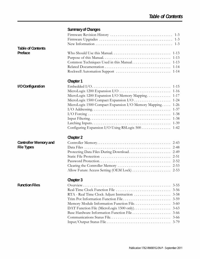
Table of Contents
Summary of ChangesFirmware Revision History . . . . . . . . . . . . . . . . . . . . . . . . . . . . . . . . . . 1-3Firmware Upgrades . . . . . . . . . . . . . . . . . . . . . . . . . . . . . . . . . . . . . . . . 1-3New Information . . . . . . . . . . . . . . . . . . . . . . . . . . . . . . . . . . . . . . . . . . 1-3
Table of ContentsPreface Who Should Use this Manual. . . . . . . . . . . . . . . . . . . . . . . . . . . . . . . . 1-13
Purpose of this Manual. . . . . . . . . . . . . . . . . . . . . . . . . . . . . . . . . . . . . 1-13Common Techniques Used in this Manual . . . . . . . . . . . . . . . . . . . . . 1-13Related Documentation . . . . . . . . . . . . . . . . . . . . . . . . . . . . . . . . . . . . 1-14Rockwell Automation Support . . . . . . . . . . . . . . . . . . . . . . . . . . . . . . 1-14
Chapter 1I/O Configuration Embedded I/O. . . . . . . . . . . . . . . . . . . . . . . . . . . . . . . . . . . . . . . . . . . 1-15
MicroLogix 1200 Expansion I/O . . . . . . . . . . . . . . . . . . . . . . . . . . . . 1-16MicroLogix 1200 Expansion I/O Memory Mapping . . . . . . . . . . . . . 1-17MicroLogix 1500 Compact Expansion I/O . . . . . . . . . . . . . . . . . . . . 1-24MicroLogix 1500 Compact Expansion I/O Memory Mapping. . . . . 1-26I/O Addressing. . . . . . . . . . . . . . . . . . . . . . . . . . . . . . . . . . . . . . . . . . . 1-37I/O Forcing . . . . . . . . . . . . . . . . . . . . . . . . . . . . . . . . . . . . . . . . . . . . . 1-38Input Filtering . . . . . . . . . . . . . . . . . . . . . . . . . . . . . . . . . . . . . . . . . . . . 1-38Latching Inputs. . . . . . . . . . . . . . . . . . . . . . . . . . . . . . . . . . . . . . . . . . . 1-39Configuring Expansion I/O Using RSLogix 500 . . . . . . . . . . . . . . . . 1-42
Chapter 2Controller Memory and File Types
Controller Memory . . . . . . . . . . . . . . . . . . . . . . . . . . . . . . . . . . . . . . . . 2-43Data Files . . . . . . . . . . . . . . . . . . . . . . . . . . . . . . . . . . . . . . . . . . . . . . . 2-48Protecting Data Files During Download. . . . . . . . . . . . . . . . . . . . . . . 2-49Static File Protection . . . . . . . . . . . . . . . . . . . . . . . . . . . . . . . . . . . . . . 2-51Password Protection. . . . . . . . . . . . . . . . . . . . . . . . . . . . . . . . . . . . . . . 2-52Clearing the Controller Memory . . . . . . . . . . . . . . . . . . . . . . . . . . . . . 2-53Allow Future Access Setting (OEM Lock) . . . . . . . . . . . . . . . . . . . . . 2-53
Chapter 3Function Files Overview. . . . . . . . . . . . . . . . . . . . . . . . . . . . . . . . . . . . . . . . . . . . . . . . 3-55
Real-Time Clock Function File . . . . . . . . . . . . . . . . . . . . . . . . . . . . . . 3-56RTA - Real Time Clock Adjust Instruction . . . . . . . . . . . . . . . . . . . . 3-58Trim Pot Information Function File . . . . . . . . . . . . . . . . . . . . . . . . . . 3-59Memory Module Information Function File. . . . . . . . . . . . . . . . . . . . 3-60DAT Function File (MicroLogix 1500 only). . . . . . . . . . . . . . . . . . . . 3-63Base Hardware Information Function File . . . . . . . . . . . . . . . . . . . . . 3-66Communications Status File. . . . . . . . . . . . . . . . . . . . . . . . . . . . . . . . . 3-66Input/Output Status File . . . . . . . . . . . . . . . . . . . . . . . . . . . . . . . . . . . 3-79
5 Publication 1762-RM001G-EN-P - September 2011

6 Table of Contents
Chapter 4Programming Instructions Overview
Instruction Set . . . . . . . . . . . . . . . . . . . . . . . . . . . . . . . . . . . . . . . . . . . . 4-81Using the Instruction Descriptions . . . . . . . . . . . . . . . . . . . . . . . . . . . . 4-82
Chapter 5Using the High-Speed Counter and Programmable Limit Switch
High-Speed Counter Overview . . . . . . . . . . . . . . . . . . . . . . . . . . . . . . . 5-87Programmable Limit Switch Overview . . . . . . . . . . . . . . . . . . . . . . . . . 5-87High-Speed Counter (HSC) Function File . . . . . . . . . . . . . . . . . . . . . . 5-87High-Speed Counter Function File Sub-Elements Summary . . . . . . . 5-89HSC Function File Sub-Elements . . . . . . . . . . . . . . . . . . . . . . . . . . . . . 5-90HSL - High-Speed Counter Load . . . . . . . . . . . . . . . . . . . . . . . . . . . . 5-110RAC - Reset Accumulated Value. . . . . . . . . . . . . . . . . . . . . . . . . . . . . 5-111Programmable Limit Switch (PLS) File. . . . . . . . . . . . . . . . . . . . . . . . 5-112
Chapter 6Using High-Speed Outputs PTO - Pulse Train Output. . . . . . . . . . . . . . . . . . . . . . . . . . . . . . . . . . 6-119
Pulse Train Output Function. . . . . . . . . . . . . . . . . . . . . . . . . . . . . . . . 6-119Pulse Train Outputs (PTO) Function File . . . . . . . . . . . . . . . . . . . . . 6-123Pulse Train Output Function File Sub-Elements Summary . . . . . . . 6-124PWM - Pulse Width Modulation . . . . . . . . . . . . . . . . . . . . . . . . . . . . . 6-137PWM Function. . . . . . . . . . . . . . . . . . . . . . . . . . . . . . . . . . . . . . . . . . . 6-137Pulse Width Modulation (PWM) Function File . . . . . . . . . . . . . . . . . 6-138Pulse Width Modulated Function File Elements Summary . . . . . . . . 6-139
Chapter 7Relay-Type (Bit) Instructions XIC - Examine if Closed
XIO - Examine if Open. . . . . . . . . . . . . . . . . . . . . . . . . . . . . . . . . . . . 7-147OTE - Output Energize. . . . . . . . . . . . . . . . . . . . . . . . . . . . . . . . . . . . 7-148OTL - Output LatchOTU - Output Unlatch . . . . . . . . . . . . . . . . . . . . . . . . . . . . . . . . . . . . 7-149ONS - One Shot. . . . . . . . . . . . . . . . . . . . . . . . . . . . . . . . . . . . . . . . . . 7-150OSR - One Shot RisingOSF - One Shot Falling . . . . . . . . . . . . . . . . . . . . . . . . . . . . . . . . . . . . 7-151
Chapter 8Timer and Counter Instructions
Timer Instructions Overview . . . . . . . . . . . . . . . . . . . . . . . . . . . . . . . 8-153TON - Timer, On-Delay . . . . . . . . . . . . . . . . . . . . . . . . . . . . . . . . . . . 8-155TOF - Timer, Off-Delay . . . . . . . . . . . . . . . . . . . . . . . . . . . . . . . . . . . 8-156RTO - Retentive Timer, On-Delay . . . . . . . . . . . . . . . . . . . . . . . . . . . 8-156How Counters Work . . . . . . . . . . . . . . . . . . . . . . . . . . . . . . . . . . . . . . 8-157CTU - Count UpCTD - Count Down. . . . . . . . . . . . . . . . . . . . . . . . . . . . . . . . . . . . . . . 8-159RES - Reset. . . . . . . . . . . . . . . . . . . . . . . . . . . . . . . . . . . . . . . . . . . . . . 8-160
Publication 1762-RM001G-EN-P - September 2011
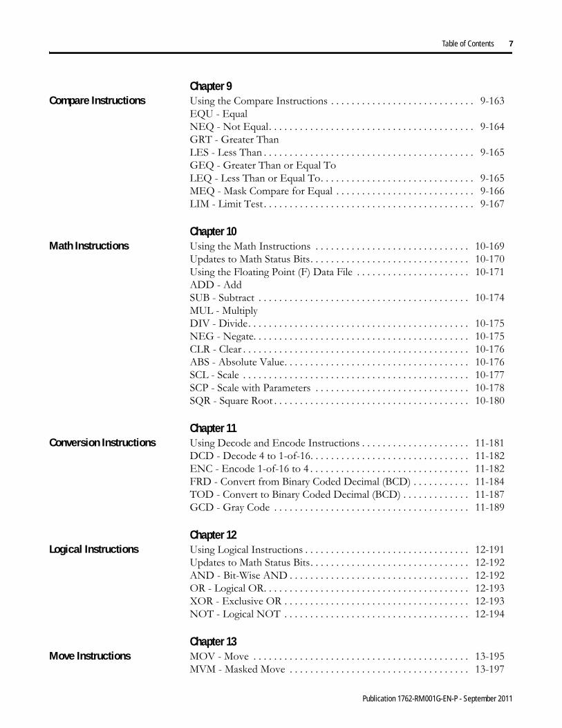
Table of Contents 7
Chapter 9Compare Instructions Using the Compare Instructions . . . . . . . . . . . . . . . . . . . . . . . . . . . . 9-163
EQU - EqualNEQ - Not Equal. . . . . . . . . . . . . . . . . . . . . . . . . . . . . . . . . . . . . . . . 9-164GRT - Greater ThanLES - Less Than . . . . . . . . . . . . . . . . . . . . . . . . . . . . . . . . . . . . . . . . . 9-165GEQ - Greater Than or Equal ToLEQ - Less Than or Equal To. . . . . . . . . . . . . . . . . . . . . . . . . . . . . . 9-165MEQ - Mask Compare for Equal . . . . . . . . . . . . . . . . . . . . . . . . . . . 9-166LIM - Limit Test . . . . . . . . . . . . . . . . . . . . . . . . . . . . . . . . . . . . . . . . . 9-167
Chapter 10Math Instructions Using the Math Instructions . . . . . . . . . . . . . . . . . . . . . . . . . . . . . . 10-169
Updates to Math Status Bits. . . . . . . . . . . . . . . . . . . . . . . . . . . . . . . 10-170Using the Floating Point (F) Data File . . . . . . . . . . . . . . . . . . . . . . 10-171ADD - AddSUB - Subtract . . . . . . . . . . . . . . . . . . . . . . . . . . . . . . . . . . . . . . . . . 10-174MUL - MultiplyDIV - Divide. . . . . . . . . . . . . . . . . . . . . . . . . . . . . . . . . . . . . . . . . . . 10-175NEG - Negate. . . . . . . . . . . . . . . . . . . . . . . . . . . . . . . . . . . . . . . . . . 10-175CLR - Clear . . . . . . . . . . . . . . . . . . . . . . . . . . . . . . . . . . . . . . . . . . . . 10-176ABS - Absolute Value. . . . . . . . . . . . . . . . . . . . . . . . . . . . . . . . . . . . 10-176SCL - Scale . . . . . . . . . . . . . . . . . . . . . . . . . . . . . . . . . . . . . . . . . . . . 10-177SCP - Scale with Parameters . . . . . . . . . . . . . . . . . . . . . . . . . . . . . . 10-178SQR - Square Root . . . . . . . . . . . . . . . . . . . . . . . . . . . . . . . . . . . . . . 10-180
Chapter 11Conversion Instructions Using Decode and Encode Instructions . . . . . . . . . . . . . . . . . . . . . 11-181
DCD - Decode 4 to 1-of-16. . . . . . . . . . . . . . . . . . . . . . . . . . . . . . . 11-182ENC - Encode 1-of-16 to 4 . . . . . . . . . . . . . . . . . . . . . . . . . . . . . . . 11-182FRD - Convert from Binary Coded Decimal (BCD) . . . . . . . . . . . 11-184TOD - Convert to Binary Coded Decimal (BCD) . . . . . . . . . . . . . 11-187GCD - Gray Code . . . . . . . . . . . . . . . . . . . . . . . . . . . . . . . . . . . . . . 11-189
Chapter 12Logical Instructions Using Logical Instructions . . . . . . . . . . . . . . . . . . . . . . . . . . . . . . . . 12-191
Updates to Math Status Bits. . . . . . . . . . . . . . . . . . . . . . . . . . . . . . . 12-192AND - Bit-Wise AND . . . . . . . . . . . . . . . . . . . . . . . . . . . . . . . . . . . 12-192OR - Logical OR. . . . . . . . . . . . . . . . . . . . . . . . . . . . . . . . . . . . . . . . 12-193XOR - Exclusive OR . . . . . . . . . . . . . . . . . . . . . . . . . . . . . . . . . . . . 12-193NOT - Logical NOT . . . . . . . . . . . . . . . . . . . . . . . . . . . . . . . . . . . . 12-194
Chapter 13Move Instructions MOV - Move . . . . . . . . . . . . . . . . . . . . . . . . . . . . . . . . . . . . . . . . . . 13-195
MVM - Masked Move . . . . . . . . . . . . . . . . . . . . . . . . . . . . . . . . . . . 13-197
Publication 1762-RM001G-EN-P - September 2011

8 Table of Contents
Chapter 14File Instructions CPW - Copy Word . . . . . . . . . . . . . . . . . . . . . . . . . . . . . . . . . . . . . . . 14-199
COP - Copy File. . . . . . . . . . . . . . . . . . . . . . . . . . . . . . . . . . . . . . . . . 14-200FLL - Fill File . . . . . . . . . . . . . . . . . . . . . . . . . . . . . . . . . . . . . . . . . . . 14-201BSL - Bit Shift Left. . . . . . . . . . . . . . . . . . . . . . . . . . . . . . . . . . . . . . . 14-203BSR - Bit Shift Right . . . . . . . . . . . . . . . . . . . . . . . . . . . . . . . . . . . . . 14-204FFL - First In, First Out (FIFO) Load . . . . . . . . . . . . . . . . . . . . . . . 14-206FFU - First In, First Out (FIFO) Unload . . . . . . . . . . . . . . . . . . . . . 14-208LFL - Last In, First Out (LIFO) Load . . . . . . . . . . . . . . . . . . . . . . . 14-210LFU - Last In, First Out (LIFO) Unload . . . . . . . . . . . . . . . . . . . . . 14-212SWP - Swap . . . . . . . . . . . . . . . . . . . . . . . . . . . . . . . . . . . . . . . . . . . . 14-214
Chapter 15Sequencer Instructions SQC- Sequencer Compare . . . . . . . . . . . . . . . . . . . . . . . . . . . . . . . . . 15-215
SQO- Sequencer Output . . . . . . . . . . . . . . . . . . . . . . . . . . . . . . . . . . 15-218SQL - Sequencer Load . . . . . . . . . . . . . . . . . . . . . . . . . . . . . . . . . . . . 15-221
Chapter 16Program Control Instructions JMP - Jump to Label . . . . . . . . . . . . . . . . . . . . . . . . . . . . . . . . . . . . . 16-223
LBL - Label. . . . . . . . . . . . . . . . . . . . . . . . . . . . . . . . . . . . . . . . . . . . . 16-224JSR - Jump to Subroutine . . . . . . . . . . . . . . . . . . . . . . . . . . . . . . . . . 16-224SBR - Subroutine Label . . . . . . . . . . . . . . . . . . . . . . . . . . . . . . . . . . . 16-224RET - Return from Subroutine . . . . . . . . . . . . . . . . . . . . . . . . . . . . . 16-225SUS - Suspend . . . . . . . . . . . . . . . . . . . . . . . . . . . . . . . . . . . . . . . . . . 16-225TND - Temporary End . . . . . . . . . . . . . . . . . . . . . . . . . . . . . . . . . . . 16-225END - Program End . . . . . . . . . . . . . . . . . . . . . . . . . . . . . . . . . . . . . 16-226MCR - Master Control Reset . . . . . . . . . . . . . . . . . . . . . . . . . . . . . . . 16-226
Chapter 17Input and Output Instructions IIM - Immediate Input with Mask . . . . . . . . . . . . . . . . . . . . . . . . . . 17-229
IOM - Immediate Output with Mask . . . . . . . . . . . . . . . . . . . . . . . . 17-230REF - I/O Refresh. . . . . . . . . . . . . . . . . . . . . . . . . . . . . . . . . . . . . . . 17-231
Chapter 18Using Interrupts Information About Using Interrupts . . . . . . . . . . . . . . . . . . . . . . . . 18-233
User Interrupt Instructions . . . . . . . . . . . . . . . . . . . . . . . . . . . . . . . . 18-237INT - Interrupt Subroutine . . . . . . . . . . . . . . . . . . . . . . . . . . . . . . . . 18-238STS - Selectable Timed Start . . . . . . . . . . . . . . . . . . . . . . . . . . . . . . . 18-238UID - User Interrupt Disable . . . . . . . . . . . . . . . . . . . . . . . . . . . . . . 18-239UIE - User Interrupt Enable . . . . . . . . . . . . . . . . . . . . . . . . . . . . . . . 18-240UIF - User Interrupt Flush . . . . . . . . . . . . . . . . . . . . . . . . . . . . . . . . 18-241Using the Selectable Timed Interrupt (STI) Function File . . . . . . . 18-242Using the Event Input Interrupt (EII) Function File. . . . . . . . . . . . 18-247
Publication 1762-RM001G-EN-P - September 2011

Table of Contents 9
Chapter 19Process Control Instruction The PID Concept . . . . . . . . . . . . . . . . . . . . . . . . . . . . . . . . . . . . . . . 19-253
The PID Equation . . . . . . . . . . . . . . . . . . . . . . . . . . . . . . . . . . . . . . 19-254PD Data File . . . . . . . . . . . . . . . . . . . . . . . . . . . . . . . . . . . . . . . . . . . 19-254PID - Proportional Integral Derivative . . . . . . . . . . . . . . . . . . . . . . 19-255Input Parameters . . . . . . . . . . . . . . . . . . . . . . . . . . . . . . . . . . . . . . . 19-256Output Parameters . . . . . . . . . . . . . . . . . . . . . . . . . . . . . . . . . . . . . . 19-259Tuning Parameters . . . . . . . . . . . . . . . . . . . . . . . . . . . . . . . . . . . . . . 19-260Runtime Errors . . . . . . . . . . . . . . . . . . . . . . . . . . . . . . . . . . . . . . . . . 19-268Analog I/O Scaling. . . . . . . . . . . . . . . . . . . . . . . . . . . . . . . . . . . . . . 19-269Application Notes. . . . . . . . . . . . . . . . . . . . . . . . . . . . . . . . . . . . . . . 19-270Application Examples . . . . . . . . . . . . . . . . . . . . . . . . . . . . . . . . . . . 19-274
Chapter 20ASCII Instructions General Information. . . . . . . . . . . . . . . . . . . . . . . . . . . . . . . . . . . . . 20-279
ASCII Instructions . . . . . . . . . . . . . . . . . . . . . . . . . . . . . . . . . . . . . . 20-279Instruction Types and Operation. . . . . . . . . . . . . . . . . . . . . . . . . . . 20-280Protocol Overview . . . . . . . . . . . . . . . . . . . . . . . . . . . . . . . . . . . . . . 20-281String (ST) Data File. . . . . . . . . . . . . . . . . . . . . . . . . . . . . . . . . . . . . 20-282Control Data File . . . . . . . . . . . . . . . . . . . . . . . . . . . . . . . . . . . . . . . 20-283ACL - ASCII Clear Buffers . . . . . . . . . . . . . . . . . . . . . . . . . . . . . . . 20-284AIC - ASCII Integer to String . . . . . . . . . . . . . . . . . . . . . . . . . . . . . 20-286AWA - ASCII Write with Append . . . . . . . . . . . . . . . . . . . . . . . . . 20-287AWT - ASCII Write . . . . . . . . . . . . . . . . . . . . . . . . . . . . . . . . . . . . . 20-289ABL - Test Buffer for Line . . . . . . . . . . . . . . . . . . . . . . . . . . . . . . . 20-291ACB - Number of Characters in Buffer . . . . . . . . . . . . . . . . . . . . . 20-293ACI - String to Integer . . . . . . . . . . . . . . . . . . . . . . . . . . . . . . . . . . . 20-294ACN - String Concatenate . . . . . . . . . . . . . . . . . . . . . . . . . . . . . . . . 20-295AEX - String Extract . . . . . . . . . . . . . . . . . . . . . . . . . . . . . . . . . . . . 20-296AHL - ASCII Handshake Lines. . . . . . . . . . . . . . . . . . . . . . . . . . . . 20-298ARD - ASCII Read Characters . . . . . . . . . . . . . . . . . . . . . . . . . . . . 20-299ARL - ASCII Read Line . . . . . . . . . . . . . . . . . . . . . . . . . . . . . . . . . . 20-301ASC - String Search . . . . . . . . . . . . . . . . . . . . . . . . . . . . . . . . . . . . . 20-302ASR - ASCII String Compare . . . . . . . . . . . . . . . . . . . . . . . . . . . . . 20-304Timing Diagram for ARD, ARL, AWA, and AWT Instructions. . 20-305Using In-line Indirection . . . . . . . . . . . . . . . . . . . . . . . . . . . . . . . . . 20-305ASCII Instruction Error Codes . . . . . . . . . . . . . . . . . . . . . . . . . . . . 20-306ASCII Character Set . . . . . . . . . . . . . . . . . . . . . . . . . . . . . . . . . . . . . 20-307
Chapter 21Communications Instructions Messaging Overview. . . . . . . . . . . . . . . . . . . . . . . . . . . . . . . . . . . . . 21-309
SVC - Service Communications. . . . . . . . . . . . . . . . . . . . . . . . . . . . 21-310MSG - Message. . . . . . . . . . . . . . . . . . . . . . . . . . . . . . . . . . . . . . . . . 21-313The Message Element . . . . . . . . . . . . . . . . . . . . . . . . . . . . . . . . . . . 21-314Timing Diagram for the MSG Instruction . . . . . . . . . . . . . . . . . . . 21-320
Publication 1762-RM001G-EN-P - September 2011

10 Table of Contents
MSG Instruction Ladder Logic . . . . . . . . . . . . . . . . . . . . . . . . . . . . . 21-323Local Messages . . . . . . . . . . . . . . . . . . . . . . . . . . . . . . . . . . . . . . . . . . 21-324Configuring a Local Message . . . . . . . . . . . . . . . . . . . . . . . . . . . . . . . 21-325Local Messaging Examples . . . . . . . . . . . . . . . . . . . . . . . . . . . . . . . . 21-333Remote Messages . . . . . . . . . . . . . . . . . . . . . . . . . . . . . . . . . . . . . . . . 21-346Configuring a Remote Message . . . . . . . . . . . . . . . . . . . . . . . . . . . . . 21-348MSG Instruction Error Codes. . . . . . . . . . . . . . . . . . . . . . . . . . . . . . 21-351
Chapter 22Recipe (MicroLogix 1500 only) and Data Logging (MicroLogix 1500 1764-LRP Processor only)
RCP - Recipe (MicroLogix 1500 only) . . . . . . . . . . . . . . . . . . . . . . . 22-359Data Logging . . . . . . . . . . . . . . . . . . . . . . . . . . . . . . . . . . . . . . . . . . . 22-364Queues and Records . . . . . . . . . . . . . . . . . . . . . . . . . . . . . . . . . . . . . 22-364Configuring Data Log Queues. . . . . . . . . . . . . . . . . . . . . . . . . . . . . . 22-368DLG - Data Log Instruction . . . . . . . . . . . . . . . . . . . . . . . . . . . . . . . 22-370Data Log Status File . . . . . . . . . . . . . . . . . . . . . . . . . . . . . . . . . . . . . . 22-370Retrieving (Reading) Records . . . . . . . . . . . . . . . . . . . . . . . . . . . . . . 22-372Accessing the Retrieval File . . . . . . . . . . . . . . . . . . . . . . . . . . . . . . . . 22-373Conditions that Will Erase the Data Retrieval File. . . . . . . . . . . . . . 22-374
Appendix AMicroLogix 1200 Memory Usage and Instruction Execution Time
Programming Instructions Memory Usage and Execution Time . . A-375MicroLogix 1200 Scan Time Worksheet. . . . . . . . . . . . . . . . . . . . . . A-380
Appendix BMicroLogix 1500 Memory Usage and Instruction Execution Time
Programming Instructions Memory usage and Execution Time . . . B-381MicroLogix 1500 Scan Time Worksheet. . . . . . . . . . . . . . . . . . . . . . B-386
Appendix CSystem Status File Status File Overview . . . . . . . . . . . . . . . . . . . . . . . . . . . . . . . . . . . . . C-389
Status File Details . . . . . . . . . . . . . . . . . . . . . . . . . . . . . . . . . . . . . . . . C-390
Appendix DFault Messages and Error Codes
Identifying Controller Faults . . . . . . . . . . . . . . . . . . . . . . . . . . . . . . . D-413Contacting Rockwell Automation for Assistance . . . . . . . . . . . . . . . D-421
Appendix EProtocol Configuration DH-485 Communication Protocol . . . . . . . . . . . . . . . . . . . . . . . . . . E-423
DF1 Full-Duplex Protocol. . . . . . . . . . . . . . . . . . . . . . . . . . . . . . . . . E-426DF1 Half-Duplex Protocol . . . . . . . . . . . . . . . . . . . . . . . . . . . . . . . . E-427DF1 Radio Modem Protocol . . . . . . . . . . . . . . . . . . . . . . . . . . . . . . . E-439Modbus RTU Protocol . . . . . . . . . . . . . . . . . . . . . . . . . . . . . . . . . . . E-447ASCII Driver . . . . . . . . . . . . . . . . . . . . . . . . . . . . . . . . . . . . . . . . . . . E-456
Publication 1762-RM001G-EN-P - September 2011
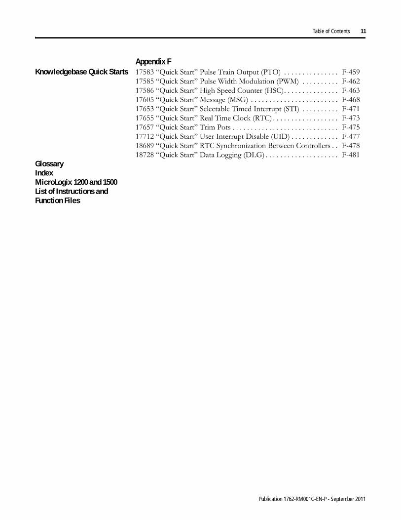
Table of Contents 11
Appendix FKnowledgebase Quick Starts 17583 “Quick Start” Pulse Train Output (PTO) . . . . . . . . . . . . . . . F-459
17585 “Quick Start” Pulse Width Modulation (PWM) . . . . . . . . . . F-46217586 “Quick Start” High Speed Counter (HSC). . . . . . . . . . . . . . . F-46317605 “Quick Start” Message (MSG) . . . . . . . . . . . . . . . . . . . . . . . . F-46817653 “Quick Start” Selectable Timed Interrupt (STI) . . . . . . . . . . F-47117655 “Quick Start” Real Time Clock (RTC) . . . . . . . . . . . . . . . . . . F-47317657 “Quick Start” Trim Pots . . . . . . . . . . . . . . . . . . . . . . . . . . . . . F-47517712 “Quick Start” User Interrupt Disable (UID) . . . . . . . . . . . . . F-47718689 “Quick Start” RTC Synchronization Between Controllers . . F-47818728 “Quick Start” Data Logging (DLG) . . . . . . . . . . . . . . . . . . . . F-481
GlossaryIndexMicroLogix 1200 and 1500 List of Instructions and Function Files
Publication 1762-RM001G-EN-P - September 2011

12 Table of Contents
Notes:
Publication 1762-RM001G-EN-P - September 2011

Preface
Read this preface to familiarize yourself with the rest of the manual. It provides information concerning:
• who should use this manual• the purpose of this manual• related documentation• conventions used in this manual• Rockwell Automation support
Who Should Use this Manual
Use this manual if you are responsible for designing, installing, programming, or troubleshooting control systems that use MicroLogix 1200 or MicroLogix 1500 controllers.
You should have a basic understanding of electrical circuitry and familiarity with relay logic. If you do not, obtain the proper training before using this product.
Purpose of this Manual This manual is a reference guide for MicroLogix 1200 and MicroLogix 1500 controllers. It describes the procedures you use to program and troubleshoot your controller. This manual:
• gives you an overview of the file types used by the controllers• provides the instruction set for the controllers• contains application examples to show the instruction set in use
Common Techniques Used in this Manual
The following conventions are used throughout this manual:
• Bulleted lists such as this one provide information, not procedural steps.• Numbered lists provide sequential steps or hierarchical information.• Italic type is used for emphasis.• Change bars appear beside information that has been changed or added
since the last revision of this manual. Change bars appear in the margin as shown to the right of this paragraph.
13 Publication 1762-RM001G-EN-P - September 2011

14 Preface
Related Documentation The following documents contain additional information concerning Rockwell Automation products. To obtain a copy, contact your local Rockwell Automation office or distributor.
Rockwell Automation Support
Before you contact Rockwell Automation for technical assistance, we suggest you please review the troubleshooting information contained in this publication first.
If the problem persists, call your local distributor or contact Rockwell Automation in one of the following ways:
For Read this Document Document NumberInformation on mounting and wiring the MicroLogix 1200 Programmable Controller, including a mounting template and door labels.
MicroLogix 1200 Programmable Controllers Installation Instructions
1762-IN006
Detailed information on planning, mounting, wiring, and troubleshooting your MicroLogix 1200 system.
MicroLogix 1200 Programmable Controllers User Manual
1762-UM001
Information on mounting and wiring the MicroLogix 1500 Base Units, including a mounting template for easy installation
MicroLogix 1500 Programmable Controllers Base Unit Installation Instructions
1764-IN001
Detailed information on planning, mounting, wiring, and troubleshooting your MicroLogix 1500 system.
MicroLogix 1500 Programmable Controllers User Manual
1764-UM001
A description on how to install and connect an AIC+. This manual also contains information on network wiring.
Advanced Interface Converter (AIC+) User Manual
1761-6.4
Information on how to install, configure, and commission a DNI DeviceNet™ Interface User Manual 1761-6.5
Information on DF1 open protocol. DF1 Protocol and Command Set Reference Manual
1770-6.5.16
In-depth information on grounding and wiring Allen-Bradley programmable controllers
Allen-Bradley Programmable Controller Grounding and Wiring Guidelines
1770-4.1
A description of important differences between solid-state programmable controller products and hard-wired electromechanical devices
Application Considerations for Solid-State Controls
SGI-1.1
An article on wire sizes and types for grounding electrical equipment National Electrical Code - Published by the National Fire Protection Association of Boston, MA.
A glossary of industrial automation terms and abbreviations Allen-Bradley Industrial Automation Glossary
AG-7.1
Phone United States/Canada 1.440.646.3434
Outside United States/Canada You can access the phone number for your country via the Internet:
1. Go to http://www.ab.com2. Click on Product Support (http://support.automation.rockwell.com)3. Under Support Centers, click on Contact Information
Internet ⇒ 1. Go to http://www.ab.com2. Click on Product Support (http://support.automation.rockwell.com)
Publication 1762-RM001G-EN-P - September 2011
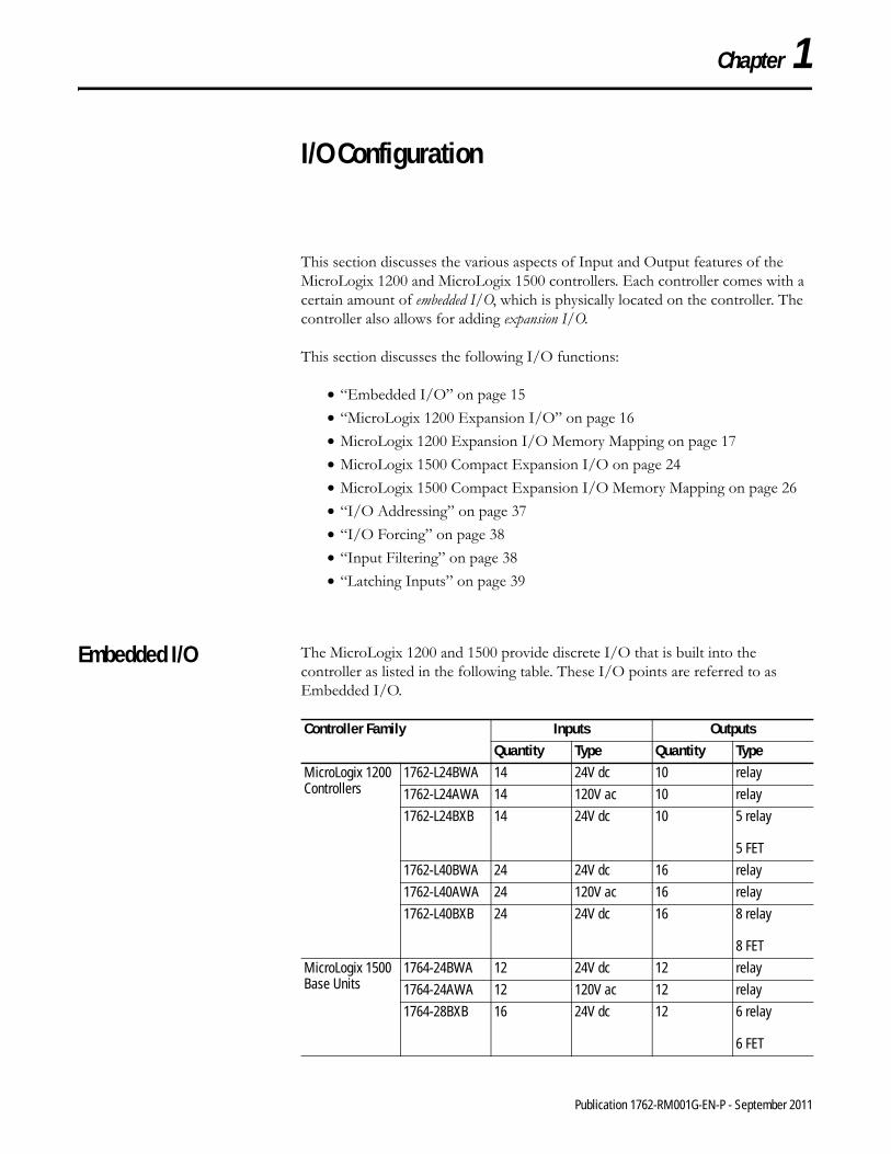
Chapter 1
I/O Configuration
This section discusses the various aspects of Input and Output features of the MicroLogix 1200 and MicroLogix 1500 controllers. Each controller comes with a certain amount of embedded I/O, which is physically located on the controller. The controller also allows for adding expansion I/O.
This section discusses the following I/O functions:
• “Embedded I/O” on page 15• “MicroLogix 1200 Expansion I/O” on page 16• MicroLogix 1200 Expansion I/O Memory Mapping on page 17• MicroLogix 1500 Compact Expansion I/O on page 24• MicroLogix 1500 Compact Expansion I/O Memory Mapping on page 26• “I/O Addressing” on page 37• “I/O Forcing” on page 38• “Input Filtering” on page 38• “Latching Inputs” on page 39
Embedded I/O The MicroLogix 1200 and 1500 provide discrete I/O that is built into the controller as listed in the following table. These I/O points are referred to as Embedded I/O.
Controller Family Inputs OutputsQuantity Type Quantity Type
MicroLogix 1200 Controllers
1762-L24BWA 14 24V dc 10 relay
1762-L24AWA 14 120V ac 10 relay
1762-L24BXB 14 24V dc 10 5 relay
5 FET
1762-L40BWA 24 24V dc 16 relay
1762-L40AWA 24 120V ac 16 relay
1762-L40BXB 24 24V dc 16 8 relay
8 FET
MicroLogix 1500 Base Units
1764-24BWA 12 24V dc 12 relay
1764-24AWA 12 120V ac 12 relay
1764-28BXB 16 24V dc 12 6 relay
6 FET
15 Publication 1762-RM001G-EN-P - September 2011

16 I/O Configuration
AC embedded inputs have fixed input filters. DC embedded inputs have configurable input filters for a number of special functions that can be used in your application. These are: high-speed counting, event interrupts, and latching inputs. The 1764-28BXB has two high-speed outputs for use as pulse train output (PTO) and/or pulse width modulation (PWM) outputs. The 1762-L24BXB and -L40BXB each have one high-speed output.
MicroLogix 1200 Expansion I/O
If the application requires more I/O than the controller provides, you can attach I/O modules. These additional modules are called expansion I/O.
Expansion I/O Modules
MicroLogix 1200 expansion I/O (Bulletin 1762) is used to provide discrete and analog inputs and outputs, and specialty modules. For the MicroLogix 1200, you can attach up to six additional I/O modules. The number of 1762 I/O modules that can be attached to the MicroLogix 1200 is dependent on the amount of power required by the I/O modules.
See the MicroLogix 1200 User Manual, publication 1762-UM001 for more information on valid configurations.
Addressing Expansion I/O Slots
The figure below shows the addressing for the MicroLogix 1200 and its I/O.
The expansion I/O is addressed as slots 1 through 6 (the controller’s embedded I/O is addressed as slot 0). Modules are counted from left to right as shown below.
TIP Visit the MicroLogix web site (http://www.ab.com/micrologix.) for the MicroLogix 1200 Expansion I/O System Qualifier.
Expansion I/O
Embedded I/O = Slot 0
Slot
1
Slot
2
Publication 1762-RM001G-EN-P - September 2011

I/O Configuration 17
MicroLogix 1200 Expansion I/O Memory Mapping
Discrete I/O Configuration
1762-IA8 and 1762-IQ8 Input Image
For each input module, the input data file contains the current state of the field input points. Bit positions 0 through 7 correspond to input terminals 0 through 7.
r = read only, x = not used, always at a 0 or OFF state
1762-IQ16 Input Image
For each input module, the input data file contains the current state of the field input points. Bit positions 0 through 15 correspond to input terminals 0 through 15.
r = read only
1762-IQ32T Input Image
For each input module, the input data file contains the current state of the field input points. Bit positions 0…15 together with word 0/1 correspond to input terminals 0…31.
r = read only
TIP In most cases, you can use the following address format: X:s/b (X = file type letter, s = slot number, b = bit number)
See I/O Addressing on page 37 for complete information on address formats.
Wor
d Bit Position15 14 13 12 11 10 9 8 7 6 5 4 3 2 1 0
0 x x x x x x x x r r r r r r r r
Wor
d Bit Position15 14 13 12 11 10 9 8 7 6 5 4 3 2 1 0
0 r r r r r r r r r r r r r r r r
Wor
d Bit Position15 14 13 12 11 10 9 8 7 6 5 4 3 2 1 0
0 r r r r r r r r r r r r r r r r
1 r r r r r r r r r r r r r r r r
Publication 1762-RM001G-EN-P - September 2011

18 I/O Configuration
1762-OX6I Output Image
For each output module, the output data file contains the controller-directed state of the discrete output points. Bit positions 0 through 5 correspond to output terminals 0 through 5.
r/w = read and write, 0 = always at a 0 or OFF state
1762-OA8, 1762-OB8, and 1762-OW8 Output Image
For each output module, the output data file contains the controller-directed state of the discrete output points. Bit positions 0 through 7 correspond to output terminals 0 through 7.
r/w = read and write, 0 = always at a 0 or OFF state
1762-OB16 and 1762-OW16 Output Image
For each output module, the output data file contains the controller-directed state of the discrete output points. Bit positions 0 through 15 correspond to output terminals 0 through 15.
r/w = read and write
1762-OV32T, 1762-OB32T Output Image
For each output module, the output data file contains the controller-directed state of the discrete output points. Bit positions 0…15 together with word 0/1 correspond to output terminals 0…31.
Wor
d Bit Position15 14 13 12 11 10 9 8 7 6 5 4 3 2 1 0
0 0 0 0 0 0 0 0 0 0 0 r/w r/w r/w r/w r/w r/wW
ord Bit Position
15 14 13 12 11 10 9 8 7 6 5 4 3 2 1 00 0 0 0 0 0 0 0 0 r/w r/w r/w r/w r/w r/w r/w r/w
Wor
d Bit Position15 14 13 12 11 10 9 8 7 6 5 4 3 2 1 0
0 r/w r/w r/w r/w r/w r/w r/w r/w r/w r/w r/w r/w r/w r/w r/w r/w
Wor
d Bit Position 15 14 13 12 11 10 9 8 7 6 5 4 3 2 1 0
0 r/w r/w r/w r/w r/w r/w r/w r/w r/w r/w r/w r/w r/w r/w r/w r/w
Publication 1762-RM001G-EN-P - September 2011

I/O Configuration 19
r/w = read and write
Analog I/O Configuration
The following table shows the data ranges for 0 to 10V dc and 4 to 20 mA.
1762-IF2OF2 Input Data File
For each input module, slot x, words 0 and 1 contain the analog values of the inputs. The module can be configured to use either raw/proportional data or scaled-for-PID data. The input data file for each configuration is shown below.
1 r/w r/w r/w r/w r/w r/w r/w r/w r/w r/w r/w r/w r/w r/w r/w r/w
Valid Input/Output Data Word Formats/Ranges
Normal Operating Range Full Scale Range Raw/Proportional Data Scaled-for-PID0 to 10V dc 10.5V dc 32760 16380
0.0V dc 0 0
4 to 20 mA 21.0 mA 32760 16380
20.0 mA 31200 15600
4.0 mA 6240 3120
0.0 mA 0 0
Raw/Proportional Format
Wor
d Bit Position15 14 13 12 11 10 9 8 7 6 5 4 3 2 1 0
0 0 Channel 0 Data 0 to 32768 0 0 01 0 Channel 1 Data 0 to 32768 0 0 02 reserved3 reserved4 reserved S1 S05 U0 O0 U1 O1 reserved
Scaled-for-PID Format
Wor
d Bit Position15 14 13 12 11 10 9 8 7 6 5 4 3 2 1 0
0 0 0 Channel 0 Data 0 to 16,383 0 01 0 0 Channel 1 Data 0 to 16,383 0 02 reserved3 reserved4 reserved S1 S05 U0 O0 U1 O1 reserved
Wor
d Bit Position 15 14 13 12 11 10 9 8 7 6 5 4 3 2 1 0
Publication 1762-RM001G-EN-P - September 2011

20 I/O Configuration
The bits are defined as follows:
• Sx = General status bits for channels 0 and 1. This bit is set when an error (over- or under-range) exists for that channel, or there is a general module hardware error.
• Ox = Over-range flag bits for channels 0 and 1. These bits can be used in the control program for error detection.
• Ux = Under-range flag bits for channels 0 and 1. These bits can be used in the control program for error detection.
1762-IF2OF2 Output Data File
For each module, slot x, words 0 and 1 contain the channel output data.
1762-IF4 Input Data File
For each module, slot x, words 0 and 1 contain the analog values of the inputs. The module can be configured to use either raw/proportional data or scaled-for-PID data. The input data file for either configuration is shown below.
Raw/Proportional Format
Wor
d Bit Position15 14 13 12 11 10 9 8 7 6 5 4 3 2 1 0
0 0 Channel 0 Data 0 to 32,768 0 0 0
1 0 Channel 1 Data 0 to 32,768 0 0 0
Scaled-for-PID Format
Wor
d Bit Position15 14 13 12 11 10 9 8 7 6 5 4 3 2 1 0
0 0 0 Channel 0 Data 0 to 16,383 0 0
1 0 0 Channel 1 Data 0 to 16,383 0 0
1762-IF4 Input Data File
Wor
d Bit Position15 14 13 12 11 10 9 8 7 6 5 4 3 2 1 0
0 SGN0 Channel 0 Data1 SGN1 Channel 1 Data2 SGN2 Channel 2 Data3 SGN3 Channel 3 Data4 reserved S3 S2 S1 S05 U0 O0 U1 O1 U2 O2 U3 O3 reserved6 reserved
Publication 1762-RM001G-EN-P - September 2011

I/O Configuration 21
The bits are defined as follows:
• Sx = General status bits for channels 0 through 3. This bit is set when an error (over- or under-range) exists for that channel, or there is a general module hardware error.
• Ox = Over-range flag bits for channels 0 through 3. These bits are set when the input signal is above the user-specified range. The module continues to convert data to the maximum full range value during an over-range condition. The bits reset when the over-range condition clears.
• UIx = Under-range flag bits for input channels 0 through 3. These bits are set when the input signal is below the user-specified range. The module continues to convert data to the maximum full range value during an under-range condition. The bits reset when the under-range condition clears.
• SGNx = The sign bit for channels 0 through 3.
1762-OF4 Input Data File
For each module, slot x, words 0 and 1 contain the analog output module status data for use in the control program.
The bits are defined as follows:
• SOx = General status bits for output channels 0 through 3. This bit is set when an error (over- or under-range) exists for that channel, or there is a general module hardware error.
• OOx = Over-range flag bits for output channels 0 through 3. These bits indicate an input signal above the user range and can be used in the control program for error detection. The module continues to convert analog data to the maximum full range value while this bit is set (1). The bit is reset (0) when the error clears.
• UOx = Under-range flag bits for output channels 0 through 3. These bits indicate an input signal below the user range. They can be used in the control program for error detection. The module continues to convert analog data to the minimum full range value while this bit is set (1). The bit is reset (0) when the error clears.
1762-OF4 Input Data File
Wor
d Bit Position15 14 13 12 11 10 9 8 7 6 5 4 3 2 1 0
0 Reserved SO3 SO2 SO1 SO0
1 Reserved UO0 OO0 UO1 OO1 UO2 OO2 UO3 OO3
Publication 1762-RM001G-EN-P - September 2011

22 I/O Configuration
1762-OF4 Output Data File
For each module, slot x, words 0 through 3 contain the channel output data.
Words 0 through 3 contain the analog output data for channels 0 through 3, respectively. The module ignores the “don’t care” bits (0 through 2), but checks the sign bit (15). If bit 15 equals 1, the module sets the output value to 0V or 0 mA.
Words 0 through 3 contain the analog output data for channels 0 through 3, respectively. The module ignores the “don’t care” bits (0 and 1), but checks the sign bit (15), and bit 14. If bit 15 equals 1, the module sets the output value to 0V or 0 mA. If bit 15 equals zero and bit 14 equals 1, the module sets the output value to 10.5V dc or 21 mA.
Specialty I/O Configuration
1762-IR4 RTD/resistance Module Input Data File
For each module, slot x, words 0 through 3 contain the analog values of the inputs. Words 4 and 5 provide sensor/channel status feedback. The input data file for each configuration is shown below.
Raw/Proportional Format
Wor
d Bit Position15 14 13 12 11 10 9 8 7 6 5 4 3 2 1 0
0 0 Channel 0 Data 0 to 32,760 0 0 0
1 0 Channel 1 Data 0 to 32,760 0 0 0
2 0 Channel 2 Data 0 to 32,760 0 0 0
3 0 Channel 3 Data 0 to 32,760 0 0 0
Scaled-for-PID Format
Wor
d Bit Position15 14 13 12 11 10 9 8 7 6 5 4 3 2 1 0
0 0 0 Channel 0 Data 0 to 16,380 0 0
1 0 0 Channel 1 Data 0 to 16,380 0 0
2 0 0 Channel 2 Data 0 to 16,380 0 0
3 0 0 Channel 3 Data 0 to 16,380 0 0
Word/Bit
15 14 13 12 11 10 9 8 7 6 5 4 3 2 1 0
0 Analog Input Data Channel 0
1 Analog Input Data Channel 1
2 Analog Input Data Channel 2
Publication 1762-RM001G-EN-P - September 2011

I/O Configuration 23
The bits are defined as follows:
• Sx = General status bits for input channels 0 through 3. This bit is set (1) when an error (over- or under-range, open-circuit or input data not valid condition) exists for that channel, or there is a general module hardware error. An input data not valid condition is determined by the user program. See the MicroLogix™ 1200 RTD/Resistance Input Module User Manual, publication number 1762-UM003, for details.
• OCx = Open-circuit indication for channels 0 through 3, using either RTD or resistance inputs. Short-circuit detection for RTD inputs only. Short-circuit detection for resistance inputs is not indicated because 0 is a valid number.
• Ox = Over-range flag bits for input channels 0 through 3, using either RTD or resistance inputs. These bits can be used in the control program for error detection.
• Ux = Under-range flag bits for channels 0 through 3, using RTD inputs only.These bits can be used in the control program for error detection. Under-range detection for direct resistance inputs is not indicated because 0 is a valid number.
1762-IT4 Thermocouple Module Input Data File
For each module, slot x, words 0 through 3 contain the analog values of the inputs. The input data file is shown below.
3 Analog Input Data Channel 3
4 Reserved OC3 OC2 OC1 OC0 Reserved S3 S2 S1 S0
5 U0 O0 U1 O1 U2 O2 U3 O3 Reserved
Word/Bit
15 14 13 12 11 10 9 8 7 6 5 4 3 2 1 0
0
SGN Analog Input Data Channel 0
1
SGN Analog Input Data Channel 1
2
SGN Analog Input Data Channel 2
3
SGN Analog Input Data Channel 3
4 Reserved OC4 OC3 OC2 OC1 OC0 Reserved S4 S3 S2 S1 S0
5 U0 O0 U1 O1 U2 O2 U3 O3 U4 O4 Reserved
Word/Bit
15 14 13 12 11 10 9 8 7 6 5 4 3 2 1 0
Publication 1762-RM001G-EN-P - September 2011
24 I/O Configuration
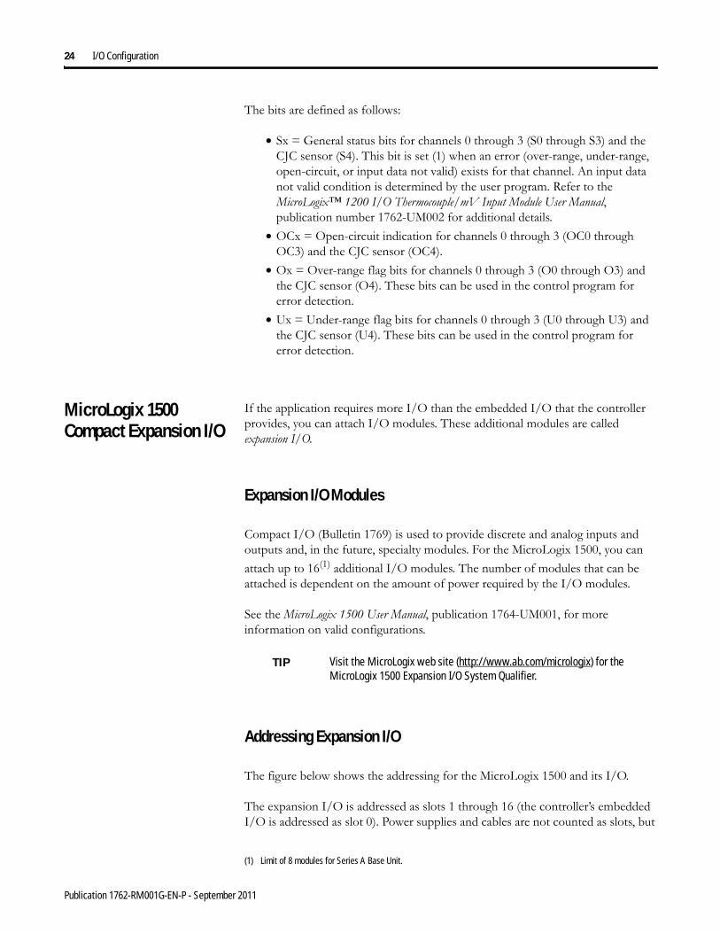
The bits are defined as follows:
• Sx = General status bits for channels 0 through 3 (S0 through S3) and the CJC sensor (S4). This bit is set (1) when an error (over-range, under-range, open-circuit, or input data not valid) exists for that channel. An input data not valid condition is determined by the user program. Refer to the MicroLogix™ 1200 I/O Thermocouple/mV Input Module User Manual, publication number 1762-UM002 for additional details.
• OCx = Open-circuit indication for channels 0 through 3 (OC0 through OC3) and the CJC sensor (OC4).
• Ox = Over-range flag bits for channels 0 through 3 (O0 through O3) and the CJC sensor (O4). These bits can be used in the control program for error detection.
• Ux = Under-range flag bits for channels 0 through 3 (U0 through U3) and the CJC sensor (U4). These bits can be used in the control program for error detection.
MicroLogix 1500 Compact Expansion I/O
If the application requires more I/O than the embedded I/O that the controller provides, you can attach I/O modules. These additional modules are called expansion I/O.
Expansion I/O Modules
Compact I/O (Bulletin 1769) is used to provide discrete and analog inputs and outputs and, in the future, specialty modules. For the MicroLogix 1500, you can attach up to 16(1) additional I/O modules. The number of modules that can be attached is dependent on the amount of power required by the I/O modules.
See the MicroLogix 1500 User Manual, publication 1764-UM001, for more information on valid configurations.
Addressing Expansion I/O
The figure below shows the addressing for the MicroLogix 1500 and its I/O.
The expansion I/O is addressed as slots 1 through 16 (the controller’s embedded I/O is addressed as slot 0). Power supplies and cables are not counted as slots, but
(1) Limit of 8 modules for Series A Base Unit.
TIP Visit the MicroLogix web site (http://www.ab.com/micrologix) for the MicroLogix 1500 Expansion I/O System Qualifier.
Publication 1762-RM001G-EN-P - September 2011

I/O Configuration 25
must be added to the RSLogix 500 project in the I/O configuration. Modules are counted from left to right on each bank as shown in the illustrations below.
Vertical Orientation
Horizontal Orientation
Expansion Power Supplies and Cables
To use a MicroLogix 1500 controller with a 1769 Expansion I/O Power Supply, verify that you have the following:
• MicroLogix 1500 Processor: Catalog Number 1764-LSP, FRN 3 and higherCatalog Number 1764-LRP, FRN 4 and higher
• Operating System Version: You can check the FRN by looking at word S:59 (Operating System FRN) in the Status File.
TIP In most cases, you can use the following address format: X:s/b (X = file type letter, s = slot number, b = bit number)
See I/O Addressing on page 37 for complete information on address formats.
Embedded I/O = Slot 0
Slot
1
Expansion
Expansion
Slot
2
Slot
3
Slot
4
Slot
5
Embedded I/O = Slot 0
Slot
1
Expansion Expansion
Slot
2
Slot
3
Slot
4
Slot
5
Publication 1762-RM001G-EN-P - September 2011

26 I/O Configuration
MicroLogix 1500 Compact Expansion I/O Memory Mapping
Discrete I/O Configuration
1769-IA8I Input Image
For each input module, the input data file contains the current state of the field input points. Bit positions 0 through 7 correspond to input terminals 0 through 7, bits 8 through 15 are not used.
r = read, x = not used, always at a 0 or OFF state
1769-IM12 Input Image
For each input module, the input data file contains the current state of the field input points. Bit positions 0 through 11 correspond to input terminals 0 through 11, bits 12 through 15 are not used.
r = read, x = not used, always at a 0 or OFF state
IMPORTANT If your processor is at an older revision, you must upgrade the operating system to FRN 3 or higher to use an expansion cable and power supply. On the Internet, go to http://www.ab.com/micrologix to download the operating system upgrade. Select MicroLogix 1500 System; go to downloads.
ATTENTION: LIMIT OF ONE EXPANSION POWER SUPPLY AND CABLE
The expansion power supply cannot be connected directly to the controller. It must be connected using one of the expansion cables. Only one expansion power supply may be used in a MicroLogix 1500 system. Exceeding these limitations may damage the power supply and result in unexpected operation.
Wor
d Bit Position15 14 13 12 11 10 9 8 7 6 5 4 3 2 1 0
0 x x x x x x x x r r r r r r r r
Wor
d Bit Position15 14 13 12 11 10 9 8 7 6 5 4 3 2 1 0
0 x x x x r r r r r r r r r r r r
Publication 1762-RM001G-EN-P - September 2011

I/O Configuration 27
1769-IA16, 1769-IQ16, and 1769-IQ16F Input Image
For each input module, the input data file contains the current state of the field input points. Bit positions 0 through 15 correspond to input terminals 0 through 15.
r = read
1769-IQ32 Input Data File
For each input module, slot x, word 0 in the input data file contains the current state of the field input points.
r = read
1769-IQ6XOW4 Input Image
For each module, the input data file contains the current state of the field input points. Bit positions 0 through 5 correspond to input terminals 0 through 5, bits 6 through 15 are not used.
r = read, x = not used, always at a 0 or OFF state
Wor
d Bit Position15 14 13 12 11 10 9 8 7 6 5 4 3 2 1 0
0 r r r r r r r r r r r r r r r rW
ord Bit Position
15 14 13 12 11 10 9 8 7 6 5 4 3 2 1 00 r r r r r r r r r r r r r r r r
1 r r r r r r r r r r r r r r r r
Wor
d Input Bit Position15 14 13 12 11 10 9 8 7 6 5 4 3 2 1 0
0 x x x x x x x x x x r r r r r r
Publication 1762-RM001G-EN-P - September 2011

28 I/O Configuration
1769-IQ6XOW4 Output Image
For each module, the output data file contains the current state of the control program’s directed state of the discrete output points. Bit positions 0 through 3 correspond to output terminals 0 through 3, bits 4 through 15 are not used.
r/w = read and write, x = not used, always at a 0 or OFF state
1769-OA8, 1769-OB8, 1769-OW8, and 1769-OW8I Output Image
For each module, the output data file contains the current state of the control program’s directed state of the discrete output points. Bit positions 0 through 7 correspond to output terminals 0 through 7, bits 8 through 15 are not used.
r/w = read and write, x = not used, always at a 0 or OFF state
1769-OA16, 1769-OB16, 1769-OB16P, 1769-OV16, and 1769-OW16 Output Image
For each module, the output data file contains the current state of the control program’s directed state of the discrete output points. Bit positions 0 through 15 correspond to output terminals 0 through 15.
r/w = read and write
1769-OB32 Output Data File
For each module, slot x, word 0 in the output data file contains the control program’s directed state of the discrete output points.
r/w = write
Wor
d Output Bit Position15 14 13 12 11 10 9 8 7 6 5 4 3 2 1 0
0 x x x x x x x x x x x x r/w r/w r/w r/wW
ord Output Bit Position
15 14 13 12 11 10 9 8 7 6 5 4 3 2 1 00 x x x x x x x x r/w r/w r/w r/w r/w r/w r/w r/w
Wor
d Output Bit Position15 14 13 12 11 10 9 8 7 6 5 4 3 2 1 0
0 r/w r/w r/w r/w r/w r/w r/w r/w r/w r/w r/w r/w r/w r/w r/w r/w
Wor
d Output Bit Position15 14 13 12 11 10 9 8 7 6 5 4 3 2 1 0
0 r/w r/w r/w r/w r/w r/w r/w r/w r/w r/w r/w r/w r/w r/w r/w r/w1 r/w r/w r/w r/w r/w r/w r/w r/w r/w r/w r/w r/w r/w r/w r/w r/w
Publication 1762-RM001G-EN-P - September 2011

I/O Configuration 29
Analog I/O Configuration
1769-IF4 Input Data File
For each input module, words 0 through 3 contain the analog values of the inputs.
The bits are defined as follows:
• SGN = Sign bit in two’s complement format.• Sx = General status bits for channels 0 through 3. This bit is set (1) when an
error (over- or under-range) exists for that channel.• Ux = Under-range flag bits for channels 0 through 3. These bits can be used
in the control program for error detection.• Ox = Over-range flag bits for channels 0 through 3. These bits can be used
in the control program for error detection.
1769-OF2 Output Data File
For each module, words 0 and 1 in the output data file contain the channel 0 and channel 1 output data.
SGN = Sign bit in two’s complement format.
Wor
d Bit Position15 14 13 12 11 10 9 8 7 6 5 4 3 2 1 0
0 SGN Analog Input Data Channel 0
1 SGN Analog Input Data Channel 1
2 SGN Analog Input Data Channel 2
3 SGN Analog Input Data Channel 3
4 not used S3 S2 S1 S0
5 U0 O0 U1 O1 U2 O2 U3 O3 Set to 0
Wor
d Bit Position15 14 13 12 11 10 9 8 7 6 5 4 3 2 1 0
0 SGN Channel 0 Data 0 to 32,768
1 SGN Channel 1 Data 0 to 32,768
Publication 1762-RM001G-EN-P - September 2011

30 I/O Configuration
1769-IF4XOF2 Input Data File
The input data file provides access to input data for use in the control program, over-range indication for the input and output channels, and output data feedback as described below.
The bits are defined as follows:
• SGN = Sign bit in two’s complement format. Always positive (equal to zero) for the 1769-IF4XOF2 module.
• Ix = Over-range flag bits for input channels 0 through 3. These bits can be used in the control program for error detection. When set to 1, the bits signal that the input signal is outside the normal operating range. However, the module continues to convert analog data to the maximum full-range value. When the over-range condition is cleared, the bits automatically reset (0).
• Ox = Word 5, bits 0 and 1 provide over-range indication for output channels 0 and 1. These bits can be used in the control program for error detection. When set to 1, the bits signal that the output signal is outside the normal operating range. However, the module continues to convert analog data to the maximum full-range value. When the over-range condition is cleared, the bits automatically reset (0).
• Ex = When set (1), this bit indicates that invalid data (e.g. the value sent by the controller is outside the standard output range or increment; e.g. 128, 256, etc.) has been set in the output data bits 0 through 6, or the sign bit (15).
Wor
d Bit Position15 14 13 12 11 10 9 8 7 6 5 4 3 2 1 0
0 SGN Analog Input Data Channel 0 0 0 0 0 0 0 0
1 SGN Analog Input Data Channel 1 0 0 0 0 0 0 0
2 SGN Analog Input Data Channel 2 0 0 0 0 0 0 0
3 SGN Analog Input Data Channel 3 0 0 0 0 0 0 0
4 Not Used(1)
(1) All unused bits are set to 0 by the module.
I3 I2 I1 I0
5 Not Used H0 Not Used H1 Not Used(1) E1 E0 O1 O0
6 SGN Output Data Echo/Loopback for Output Channel 0 0 0 0 0 0 0 0
7 SGN Output Data Echo/Loopback for Output Channel 1 0 0 0 0 0 0 0
IMPORTANT Input words 6 and 7 contain the Output Data Echo/Loopback information for output channels 0 and 1 respectively. Bits 0 through 6 and Bit 15 of words 6 and 7 should always be set to zero in your control program. If they are not set to 0, the invalid data flag (Ex) will be set for that channel by the module. However the channel will continue to operate with the previously converted value.
TIP Under-range indication is not provided because zero is a valid number.
Publication 1762-RM001G-EN-P - September 2011

I/O Configuration 31
• Hx = Hold Last State bits. When set (1), these bits indicate that the channel is in a Hold Last State condition.
• Words 6 and 7 = These words reflect the analog output data echo of the analog value being converted by the digital/analog converter, not necessarily the electrical state of the output terminals. They do not reflect shorted or open outputs.
1769-IF4XOF2 Output Data File
The output data file applies only to output data from the module as shown in the table below.
Specialty I/O Configuration
1769-IR6 RTD/resistance Module Input Data File
The first six words (0 to 5) of the input data file contain the analog RTD or resistance values of the inputs. Words 6 and 7 provide sensor/channel status feedback for use in your control program as shown below.
IMPORTANT It is only important to use the loopback function of input words 6 and 7 if the controller supports the Program Mode or Fault Mode functions, and if it is configured to use them.
Wor
d Bit Position15 14 13 12 11 10 9 8 7 6 5 4 3 2 1 0
0 SGN Analog Output Data Channel 0 0 0 0 0 0 0 0
1 SGN Analog Output Data Channel 1 0 0 0 0 0 0 0
IMPORTANT Bits 0 through 6 and Bit 15 of output data words 0 and 1 should always be set to zero in your control program. If they are not set to 0, the invalid data flag (Ex) will be set for that channel. However the channel will continue to operate with the previously converted value. If a MVM (Move with Mask) instruction is used with a mask of 7F80 (hexidecimal) to move data to the output words, writing to bits 0 through 6 and bit 15 can be avoided.
Wor
d Bit Position15 14 13 12 11 10 9 8 7 6 5 4 3 2 1 0
0 RTD/resistance Input Data Channel 01 RTD/resistance Input Data Channel 12 RTD/resistance Input Data Channel 23 RTD/resistance Input Data Channel 34 RTD/resistance Input Data Channel 4
Publication 1762-RM001G-EN-P - September 2011
32 I/O Configuration
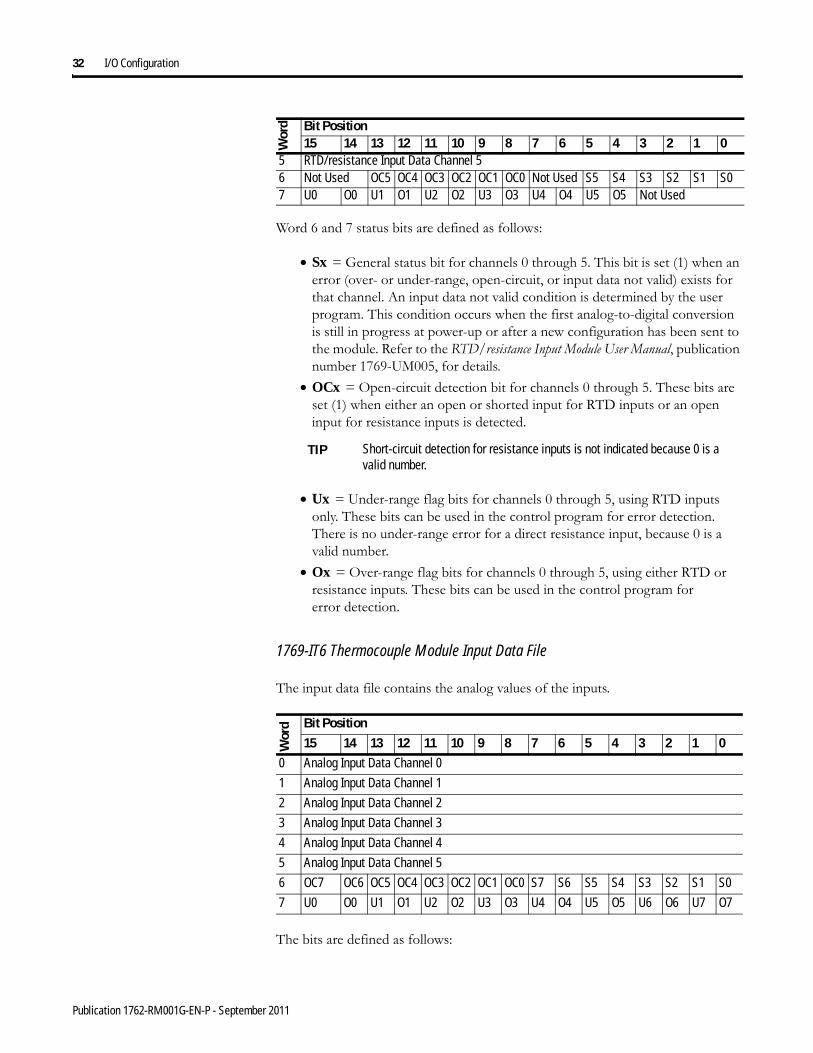
Word 6 and 7 status bits are defined as follows:
• Sx = General status bit for channels 0 through 5. This bit is set (1) when an error (over- or under-range, open-circuit, or input data not valid) exists for that channel. An input data not valid condition is determined by the user program. This condition occurs when the first analog-to-digital conversion is still in progress at power-up or after a new configuration has been sent to the module. Refer to the RTD/resistance Input Module User Manual, publication number 1769-UM005, for details.
• OCx = Open-circuit detection bit for channels 0 through 5. These bits are set (1) when either an open or shorted input for RTD inputs or an open input for resistance inputs is detected.
• Ux = Under-range flag bits for channels 0 through 5, using RTD inputs only. These bits can be used in the control program for error detection. There is no under-range error for a direct resistance input, because 0 is a valid number.
• Ox = Over-range flag bits for channels 0 through 5, using either RTD or resistance inputs. These bits can be used in the control program for error detection.
1769-IT6 Thermocouple Module Input Data File
The input data file contains the analog values of the inputs.
The bits are defined as follows:
5 RTD/resistance Input Data Channel 56 Not Used OC5 OC4 OC3 OC2 OC1 OC0 Not Used S5 S4 S3 S2 S1 S07 U0 O0 U1 O1 U2 O2 U3 O3 U4 O4 U5 O5 Not Used
TIP Short-circuit detection for resistance inputs is not indicated because 0 is a valid number.
Wor
d Bit Position15 14 13 12 11 10 9 8 7 6 5 4 3 2 1 0
0 Analog Input Data Channel 0
1 Analog Input Data Channel 1
2 Analog Input Data Channel 2
3 Analog Input Data Channel 3
4 Analog Input Data Channel 4
5 Analog Input Data Channel 5
6 OC7 OC6 OC5 OC4 OC3 OC2 OC1 OC0 S7 S6 S5 S4 S3 S2 S1 S0
7 U0 O0 U1 O1 U2 O2 U3 O3 U4 O4 U5 O5 U6 O6 U7 O7
Wor
d Bit Position15 14 13 12 11 10 9 8 7 6 5 4 3 2 1 0
Publication 1762-RM001G-EN-P - September 2011

I/O Configuration 33
• Sx = General status bit for channels 0 through 5 and CJC sensors (S6 and S7). This bit is set (1) when an error (over-range, under-range, open-circuit, or input data not valid) exists for that channel. An input data not valid condition is determined by the user program. This condition occurs when the first analog-to-digital conversion is still in progress, after a new configuration has been sent to the module.
• OCx = Open circuit detection bits indicate an open input circuit on channels 0 through 5 (OC0 through OC5) and on CJC sensors CJC0 (OC6) and CJC1 (OC7). The bit is set (1) when an open-circuit condition exists.
• Ux = Under-range flag bits for channels 0 through 5 and the CJC sensors (U6 and U7). For thermocouple inputs, the under-range bit is set when a temperature measurement is below the normal operating range for a given thermocouple type. For millivolt inputs, the under-range bit indicates a voltage that is below the normal operating range. These bits can be used in the control program for error detection.
• Ox = Over-range flag bits for channels 0 through 5 and the CRC sensors (O6 and O7). For thermocouple inputs, the over-range bit is set when a temperature measurement is above the normal operating range for a given thermocouple type. For millivolt inputs, the over-range bit indicates a voltage that is above the normal operating range. These bits can be used in the control program for error detection.
1769-HSC High-Speed Counter Module Output Array
The information in the following table is a quick reference of the array. Refer to the Compact I/O High Speed Counter User Manual, publication 1769-UM006, for detailed information.
The default value for the Output Array is all zeros.
15 14 13 12 11 10 9 8 7 6 5 4 3 2 1 0 Description
0 Out15 Out14 Out13 Out12 Out11 Out10 Out09 Out08 Out07 Out06 Out05 Out04 Out03 Out02 Out01 Out00 OutputOnMask.0 -- OutputOnMask.15
1 Out15 Out14 Out13 Out12 Out11 Out10 Out09 Out08 Out07 Out06 Out05 Out04 Out03 Out02 Out01 Out00 OutputOffMask.0 -- OutputOffMask.15
2 R15 R14 R13 R12 R11 R10 R09 R08 R07 R06 R05 R04 R03 R02 R01 R00 RangeEn.0 -- RangeEn.15
3 Reserved
4 RBF ResetBlownFuse
5 RPW RREZ Z Inh Z Inv D Inh D Inv RCU RCO SP En Ctr0ControlBits → Ctr0En
Ctr0SoftPreset
Ctr0ResetCountOverflow
Ctr0ResetCountUnderflow
Ctr0DirectionInvert
Ctr0DirectionInhibit
Ctr0ZInvert
Ctr0ZInhibit
Ctr0ResetRisingEdgeZ
Ctr0ResetCtrPresetWarning
6 RPW RREZ Z Inh Z Inv D Inh D Inv RCU RCO SP En Ctr1ControlBits
7 RPW D Inv RCU RCO SP En Ctr2ControlBits
8 RPW D Inv RCU RCO SP En Ctr3ControlBits
9 Reserved
10
11Range12To15[0].HiLimOrDirWr Range12To15[0].HiLimOrDirWr
12
13Range12To15[0].LowLimit Range12To15[0].LowLimit
14 Out15 Out14 Out13 Out12 Out11 Out10 Out09 Out08 Out07 Out06 Out05 Out04 Out03 Out02 Out01 Out00 Range12To15[0].OutputControl.0 ... .15
Publication 1762-RM001G-EN-P - September 2011

34 I/O Configuration
1769-HSC High-Speed Counter Module Input Array
The information in the following table is a quick reference of the array. Refer to the Compact I/O High Speed Counter User Manual, publication 1769-UM006, for detailed information.
The default value for the Input Array is all zeros.
15 Inv LDW Type ToThisCtr Range12To15[0].Config Flags → Range12To15[0].ToThisCounter_0
Range12To15[0].ToThisCounter_1
Range12To15[0].Type
Range12To15[0].LoadDirectWrite
Range12To15[0].Invert
16
17Range12To15[1].HiLimOrDirWr Range12To15[1].HiLimOrDirWr
18
19Range12To15[1].LowLimit Range12To15[1].LowLimit
20 Out15 Out14 Out13 Out12 Out11 Out10 Out09 Out08 Out07 Out06 Out05 Out04 Out03 Out02 Out01 Out00 Range12To15[1].OutputControl.0 ... .15
21 Inv LDW Type ToThisCtr Range12To15[1].Config Flags → Range12To15[1].ToThisCounter_0
Range12To15[1].ToThisCounter_1
Range12To15[1].Type
Range12To15[1].LoadDirectWrite
Range12To15[1].Invert
22
23Range12To15[2].HiLimOrDirWr Range12To15[2].HiLimOrDirWr
24
25Range12To15[2].LowLimit Range12To15[2].LowLimit
26 Out15 Out14 Out13 Out12 Out11 Out10 Out09 Out08 Out07 Out06 Out05 Out04 Out03 Out02 Out01 Out00 Range12To15[2].OutputControl.0 ... .15
27 Inv LDW Type ToThisCtr Range12To15[2].Config Flags → Range12To15[2].ToThisCounter_0
Range12To15[2].ToThisCounter_1
Range12To15[2].Type
Range12To15[2].LoadDirectWrite
Range12To15[2].Invert
28
29Range12To15[3].HiLimOrDirWr Range12To15[3].HiLimOrDirWr
30
31Range12To15[3].LowLimit Range12To15[3].LowLimit
32 Out15 Out14 Out13 Out12 Out11 Out10 Out09 Out08 Out07 Out06 Out05 Out04 Out03 Out02 Out01 Out00 Range12To15[3].OutputControl.0 ... .15
33 Inv LDW Type ToThisCtr Range12To15[3].Config Flags → Range12To15[3].ToThisCounter_0
Range12To15[3].ToThisCounter_1
Range12To15[3].Type
Range12To15[3].LoadDirectWrite
Range12To15[3].Invert
15 14 13 12 11 10 9 8 7 6 5 4 3 2 1 0 Description
0 Z1 B1 A1 Z0 B0 A0 InputStateA0 -- InputStateZ1
1 Out15 Out14 Out13 Out12 Out11 Out10 Out09 Out08 Out07 Out06 Out05 Out04 Out03 Out02 Out01 Out00 Readback.0 -- Readback.15
2 InvalidRangeLimit12…15 InvalidCtrAssignToRange12…15 GenErr InvOut MCfg Out0Overcurrent -- Out3… Status Flags → InvalidRangeLimit12 ... 15
InvalidCtrAssignToRange12 ... 15
GenError
InvalidOutput
ModConfig
Out0Overcurrent0 ... 3
3 R15 R14 R13 R12 R11 R10 R09 R08 R07 R06 R05 R04 R03 R02 R01 R00 RangeActive.0 -- RangeActive.15
4
5Ctr[0].CurrentCount Ctr[0].CurrentCount
6
7Ctr[0].StoredCount Ctr[0].StoredCount
8
9Ctr[0].CurrentRate Ctr[0].CurrentRate
10
11Ctr[0].PulseInterval Ctr[0].PulseInterval
Publication 1762-RM001G-EN-P - September 2011

I/O Configuration 35
1769-SDN DeviceNet Scanner Module Data Organization
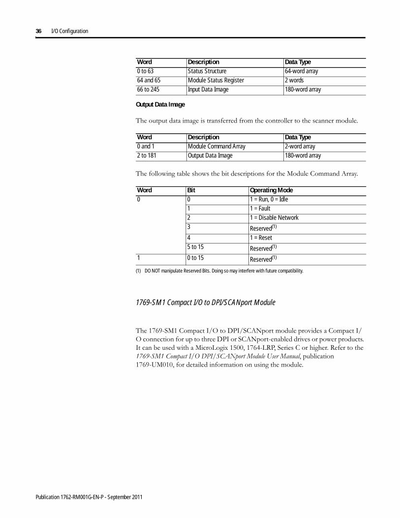
The scanner uses the input and output data images to transfer data, status and command information between the scanner and the controller. The basic structure is shown below. Refer to the Compact I/O DeviceNet Scanner Module User Manual, publication 1769-UM009, for more detailed information.
Input Data Image
The input data image is transferred from the scanner module to the controller.
12 C0PW RV IDW REZ CUdf COvf Ctr[0].StatusFlags → Ctr[0].Overflow
Ctr[0].Underflow
Ctr[0].RisingEdgeZ
Ctr[0].InvalidDirectWrite
----------------
Ctr[0].RateValid
Ctr[0].PresetWarning
13 Reserved
14
15Ctr[1].CurrentCount Ctr[1].CurrentCount
16
17Ctr[1].StoredCount Ctr[1].StoredCount
18
19Ctr[1].CurrentRate Ctr[1].CurrentRate
20
21Ctr[1].PulseInterval Ctr[1].PulseInterval
22 C1PW RV IC IDW REZ CUdf COvf Ctr[1].StatusFlags → Ctr[1].Overflow
Ctr[1].Underflow
Ctr[1].RisingEdgeZ
Ctr[1].InvalidDirectWrite
Ctr[1].InvalidCounter
Ctr[1].RateValid
Ctr[1].PresetWarning
23 Reserved
24
25Ctr[2].CurrentCount Ctr[2].CurrentCount
26
27Ctr[2].CurrentRate Ctr[2].CurrentRate
28 C2PW RV IC IDW CUdf COvf Ctr[2].StatusFlags → Ctr[2].Overflow
Ctr[2].Underflow
----------------
Ctr[2].InvalidDirectWrite
Ctr[2].InvalidCounter
Ctr[2].RateValid
Ctr[2].PresetWarning
29 Reserved
30
31Ctr[3].CurrentCount Ctr[3].CurrentCount
32
33Ctr[3].CurrentRate Ctr[3].CurrentRate
34 C3PW RV IC IDW CUdf COvf Ctr[3].StatusFlags → Ctr[3].Overflow
Ctr[3].Underflow
----------------
Ctr[3].InvalidDirectWrite
Ctr[3].InvalidCounter
Ctr[3].RateValid
Ctr[3].PresetWarning
Publication 1762-RM001G-EN-P - September 2011
36 I/O Configuration
Output Data Image
The output data image is transferred from the controller to the scanner module.
The following table shows the bit descriptions for the Module Command Array.
1769-SM1 Compact I/O to DPI/SCANport Module
The 1769-SM1 Compact I/O to DPI/SCANport module provides a Compact I/O connection for up to three DPI or SCANport-enabled drives or power products. It can be used with a MicroLogix 1500, 1764-LRP, Series C or higher. Refer to the 1769-SM1 Compact I/O DPI/SCANport Module User Manual, publication 1769-UM010, for detailed information on using the module.
Word Description Data Type0 to 63 Status Structure 64-word array64 and 65 Module Status Register 2 words66 to 245 Input Data Image 180-word array
Word Description Data Type0 and 1 Module Command Array 2-word array2 to 181 Output Data Image 180-word array
Word Bit Operating Mode0 0 1 = Run, 0 = Idle
1 1 = Fault2 1 = Disable Network3 Reserved(1)
(1) DO NOT manipulate Reserved Bits. Doing so may interfere with future compatibility.
4 1 = Reset5 to 15 Reserved(1)
1 0 to 15 Reserved(1)
Publication 1762-RM001G-EN-P - September 2011
I/O Configuration 37
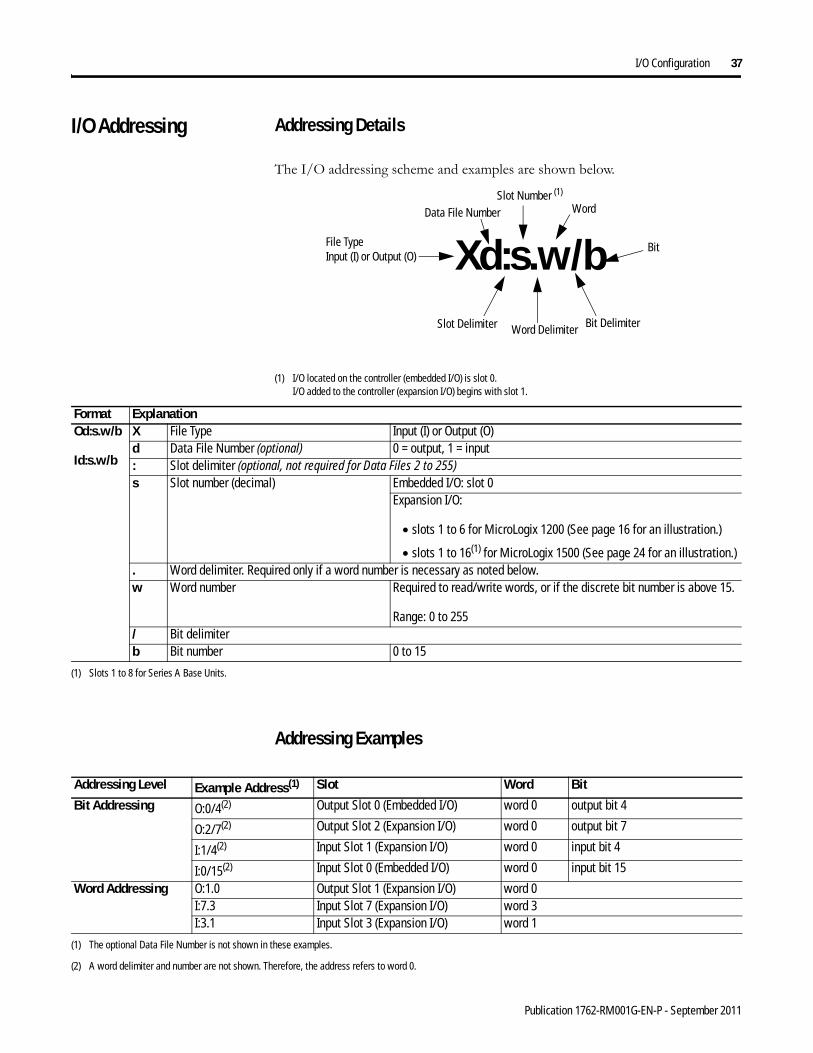
I/O Addressing Addressing Details
The I/O addressing scheme and examples are shown below.
(1) I/O located on the controller (embedded I/O) is slot 0. I/O added to the controller (expansion I/O) begins with slot 1.
Addressing Examples
Xd:s.w/bFile Type Input (I) or Output (O)
Data File NumberSlot Number (1)
Word
Bit
Bit DelimiterWord DelimiterSlot Delimiter
Format ExplanationOd:s.w/b
Id:s.w/b
X File Type Input (I) or Output (O)d Data File Number (optional) 0 = output, 1 = input: Slot delimiter (optional, not required for Data Files 2 to 255)s Slot number (decimal) Embedded I/O: slot 0
Expansion I/O:
• slots 1 to 6 for MicroLogix 1200 (See page 16 for an illustration.)
• slots 1 to 16(1) for MicroLogix 1500 (See page 24 for an illustration.). Word delimiter. Required only if a word number is necessary as noted below.w Word number Required to read/write words, or if the discrete bit number is above 15.
Range: 0 to 255/ Bit delimiterb Bit number 0 to 15
(1) Slots 1 to 8 for Series A Base Units.
Addressing Level Example Address(1) Slot Word Bit
Bit Addressing O:0/4(2) Output Slot 0 (Embedded I/O) word 0 output bit 4
O:2/7(2) Output Slot 2 (Expansion I/O) word 0 output bit 7
I:1/4(2) Input Slot 1 (Expansion I/O) word 0 input bit 4
I:0/15(2) Input Slot 0 (Embedded I/O) word 0 input bit 15
Word Addressing O:1.0 Output Slot 1 (Expansion I/O) word 0I:7.3 Input Slot 7 (Expansion I/O) word 3I:3.1 Input Slot 3 (Expansion I/O) word 1
(1) The optional Data File Number is not shown in these examples.
(2) A word delimiter and number are not shown. Therefore, the address refers to word 0.
Publication 1762-RM001G-EN-P - September 2011

38 I/O Configuration
I/O Forcing I/O forcing is the ability to override the actual status of the I/O at the user’s discretion.
Input Forcing
When an input is forced, the value in the input data file is set to a user-defined state. For discrete inputs, you can force an input “on” or “off ”. When an input is forced, it no longer reflects the state of the physical input or the input LED. For embedded inputs, the controller reacts as if the force is applied to the physical input terminal.
Output Forcing
When an output is forced, the controller overrides the status of the control program, and sets the output to the user-defined state. Discrete outputs can be forced “on” or “off ”. The value in the output file is unaffected by the force. It maintains the state determined by the logic in the control program. However, the state of the physical output and the output LED will be set to the forced state.
Input Filtering The MicroLogix 1200 and 1500 controllers allow users to configure groups of DC inputs for high-speed or normal operation. Users can configure each input group’s response time. A configurable filter determines how long the input signal must be “on” or “off ” before the controller recognizes the signal. The higher the value, the longer it takes for the input state to be recognized by the controller. Higher values provide more filtering, and are used in electrically noisy environments. Lower values provide less filtering, and are used to detect fast or narrow pulses. You typically set the filters to a lower value when using high-speed counters, latching inputs, and input interrupts.
Input filtering is configured using RSLogix 500 programming software. To configure the filters using RSLogix 500:
1. Open the “Controller” folder.
2. Open the “I/O Configuration” folder.
3. Open slot 0 (controller).
TIP When an input is forced, it has no effect on the input device connected to the controller.
TIP If you force an output controlled by an executing PTO or PWM function, an instruction error is generated.
Publication 1762-RM001G-EN-P - September 2011

I/O Configuration 39
4. Select the “embedded I/O configuration” tab.
The input groups are pre-arranged. Simply select the filter time you require for each input group. You can apply a unique input filter setting to each of the input groups:
The minimum and maximum response times associated with each input filter setting can be found in your controller’s User Manual.
Latching Inputs The MicroLogix 1200 and 1500 controllers provide the ability to individually configure inputs to be latching inputs (sometimes referred to as pulse catching inputs). A latching input is an input that captures a very fast pulse and holds it for a single controller scan. The pulse width that can be captured is dependent upon the input filtering selected for that input.
The following inputs can be configured as latching inputs:
You enable this feature with RSLogix 500 programming software. With an open project:
1. Open the “Controller” folder.
2. Open the “I/O Configuration” folder.
3. Open slot 0 (controller).
4. Select the “embedded I/O configuration” tab.
5. Select the mask bits for the inputs that you want to operate as latching inputs.
6. Select the state for the latching inputs. The controller can detect both “on” (rising edge) and “off ” (falling edge) pulses, depending upon the configuration selected in the programming software.
Controller MicroLogix 1200 MicroLogix 1500Input Groups • 0 and 1
• 2 and 3
• 4 and above
• 0 and 1
• 2 and 3
• 4 and 5
• 6 and 7
• 8 and above
Controller MicroLogix 1200 MicroLogix 1500DC Inputs 0 through 3 0 through 7
Publication 1762-RM001G-EN-P - September 2011

40 I/O Configuration
The following information is provided for a controller looking for an “on” pulse. When an external signal is detected “on”, the controller “latches” this event. In general, at the next input scan following this event, the input image point is turned “on” and remains “on” for the next controller scan. It is then set to “off ” at the next input scan. The following figures help demonstrate this.
Rising Edge Behavior - Example 1
Rising Edge Behavior - Example 2
TIP The “gray” area of the Latched Status waveform is the input filter delay.
IMPORTANT The input file value does not represent the external input when the input is configured for latching behavior. When configured for rising edge behavior, the input file value is normally “off” (“on” for 1 scan when a rising edge pulse is detected).
Scan Number (X) Scan Number (X+1) Scan Number (X+2)
ExternalInput
LatchedStatus
Input FileValue
InputScan
LadderScan
OutputScan
InputScan
LadderScan
OutputScan
InputScan
LadderScan
OutputScan
Scan Number (X) Scan Number (X+1) Scan Number (X+2)
ExternalInput
LatchedStatus
Input FileValue
InputScan
LadderScan
OutputScan
InputScan
LadderScan
OutputScan
InputScan
LadderScan
OutputScan
Publication 1762-RM001G-EN-P - September 2011

I/O Configuration 41
The previous examples demonstrate rising edge behavior. Falling edge behavior operates exactly the same way with these exceptions:
• The detection is on the “falling edge” of the external input.• The input image is normally “on” (1), and changes to “off ” (0) for one scan.
Falling Edge Behavior - Example 1
Falling Edge Behavior - Example 2
TIP The “gray” area of the Latched Status waveform is the input filter delay.
IMPORTANT The input file value does not represent the external input when the input is configured for latching behavior. When configured for falling edge behavior, the input file value is normally “on” (“off” for 1 scan when a falling edge pulse is detected).
Scan Number (X) Scan Number (X+1) Scan Number (X+2)
ExternalInput
LatchedStatus
Input FileValue
InputScan
LadderScan
OutputScan
Scan Number (X+3)
InputScan
LadderScan
OutputScan
InputScan
LadderScan
OutputScan
InputScan
LadderScan
OutputScan
Scan Number (X) Scan Number (X+1) Scan Number (X+2)
ExternalInput
LatchedStatus
Input FileValue
InputScan
LadderScan
OutputScan
InputScan
LadderScan
OutputScan
InputScan
LadderScan
OutputScan
Publication 1762-RM001G-EN-P - September 2011

42 I/O Configuration
Configuring Expansion I/O Using RSLogix 500
Expansion I/O must be configured for use with the controller. Configuring expansion I/O can be done either manually, or automatically. Using RSLogix 500:
1. Open the “Controller” folder.
2. Open the “I/O Configuration” folder.
3. For manual configuration, drag the Compact I/O module to the slot.
For automatic configuration, you must have the controller connected online to the computer (either directly or over a network). Click the “Read I/O Config” button on the I/O configuration screen. RSLogix 500 will read the existing configuration of the controller’s I/O.
Some I/O modules support or require configuration. To configure a specific module, double-click on the module, an I/O configuration screen will open that is specific to the module.
Publication 1762-RM001G-EN-P - September 2011

Chapter 2
Controller Memory and File Types
This chapter describes controller memory and the types of files used by the MicroLogix 1200 and MicroLogix 1500 controllers. The chapter is organized as follows:
• “Controller Memory” on page 43• “Data Files” on page 48• “Protecting Data Files During Download” on page 49• “Static File Protection” on page 51• “Password Protection” on page 52• “Clearing the Controller Memory” on page 53• “Allow Future Access Setting (OEM Lock)” on page 53
Controller Memory File Structure
MicroLogix 1200 and 1500 user memory is comprised of Data Files, Function Files, and Program Files (and B-Ram files for the MicroLogix 1500 1764-LRP processor). Function Files are exclusive to the MicroLogix 1200 and 1500 controllers; they are not available in the MicroLogix 1000 or SLC controllers.
TIP The file types shown below for data files 3 through 7 are the default filetypes for those file numbers and cannot be changed. Data files 9 through 255 can be added to your program to operate as bit, timer, counter, control, integer, string, long word, message, or PID files.
Data Files Function Files Program Files Specialty Files(1)
0 Output File HSC High Speed Counter 0 System File 0 0 Data Log Queue 0
1 Input File PTO(2) Pulse Train Output 1 System File 1 1 Data Log Queue 1
2 Status File PWM(2) Pulse Width Modulation
2 Program File 2 2 to 255 Data Log Queues 2 to 255
43 Publication 1762-RM001G-EN-P - September 2011

44 Controller Memory and File Types
User Memory
User memory is the amount of storage available to a user for storing ladder logic, data table files, I/O configuration, etc., in the controller.
User data files consist of the system status file, I/O image files, and all other user-creatable data files (bit, timer, counter, control, integer, string, long word, MSG, and PID).
3 Bit File STI Selectable Timed Interrupt
3 to 255 Program Files 3 to 255 0 Recipe File 0
4 Timer File EII Event Input Interrupt 1 Recipe File 1
5 Counter File RTC Real Time Clock 2 to 255 Recipe Files 2 to 255
6 Control File TPI Trim Pot Information
7 Integer File MMI Memory Module Information
8 Floating Point File DAT(3) Data Access Tool
9 to 255 (B) Bit
(T) Timer
(C) Counter
(R) Control
(N) Integer
(F) Floating Point(4)
(ST) String(5)
(L) Long Word
(MG) Message
(PD) PID
(PLS) Programmable Limit Switch(4)
BHI Base Hardware Information
CS Communications Status
IOS I/O Status
DLS(1) Data Log Status
(1) Specialty files for Data Logging are only used by the MicroLogix 1500 1764-LRP processor. Specialty files for Recipes are only used by MicroLogix 1500 Series C processors.
(2) The PTO and PWM files are only used in MicroLogix 1200 and 1500 BXB units.
(3) The DAT files are only used in MicroLogix 1500 controllers.
(4) The floating point and programmable limit switch files are available in MicroLogix 1200 and 1500 Series C controllers.
(5) The string file is available in MicroLogix 1200 controllers and MicroLogix 1500 1764-LSP Series B (and later) and 1764-LRP processors.
Data Files Function Files Program Files Specialty Files(1)
Publication 1762-RM001G-EN-P - September 2011
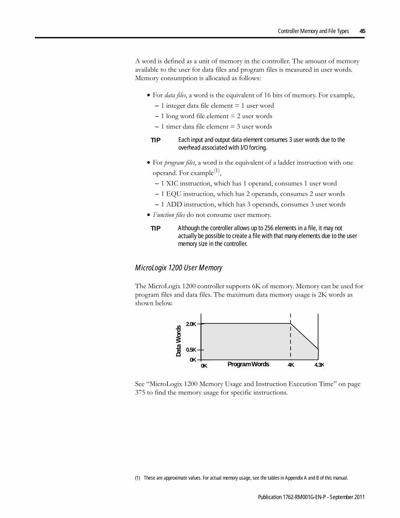
Controller Memory and File Types 45
A word is defined as a unit of memory in the controller. The amount of memory available to the user for data files and program files is measured in user words. Memory consumption is allocated as follows:
• For data files, a word is the equivalent of 16 bits of memory. For example,– 1 integer data file element = 1 user word– 1 long word file element = 2 user words– 1 timer data file element = 3 user words
• For program files, a word is the equivalent of a ladder instruction with one operand. For example(1),– 1 XIC instruction, which has 1 operand, consumes 1 user word– 1 EQU instruction, which has 2 operands, consumes 2 user words– 1 ADD instruction, which has 3 operands, consumes 3 user words
• Function files do not consume user memory.
MicroLogix 1200 User Memory
The MicroLogix 1200 controller supports 6K of memory. Memory can be used for program files and data files. The maximum data memory usage is 2K words as shown below.
See “MicroLogix 1200 Memory Usage and Instruction Execution Time” on page 375 to find the memory usage for specific instructions.
TIP Each input and output data element consumes 3 user words due to the overhead associated with I/O forcing.
(1) These are approximate values. For actual memory usage, see the tables in Appendix A and B of this manual.
TIP Although the controller allows up to 256 elements in a file, it may not actually be possible to create a file with that many elements due to the user memory size in the controller.
2.0K
0.5K
0K0K 4K 4.3K
Dat
a W
ords
Program Words
Publication 1762-RM001G-EN-P - September 2011

46 Controller Memory and File Types
MicroLogix 1500 User Memory
MicroLogix 1500, 1764-LSP Processor
The 1764-LSP processor supports over 7K of memory. Memory can be used for program files and data files. The maximum data memory usage is 4K words as shown below.
MicroLogix 1500, 1764-LRP Processor
The 1764-LRP processor supports 14K of memory. Memory can be used for program files and data files. The maximum data memory usage is 4K words as shown below.
The 1764-LRP processor also supports 48K bytes of battery backed memory for Data Logging or Recipe operations. See Chapter 22 for Data Logging and Recipe information.
See “MicroLogix 1500 Memory Usage and Instruction Execution Time” on page 381 to find the memory usage for specific instructions.
IMPORTANT For the MicroLogix 1500, the maximum file size of any single ladder file is 6.4K words. You can utilize the entire programming space by using multiple ladder files through the use of subroutines.
4.0K
0.5K
0K0K 3.65K 4.35K
Dat
a W
ords
Program Words
4.0K
0.5K
0K0K 10K 10.7K
Dat
a W
ords
Program Words
Publication 1762-RM001G-EN-P - September 2011
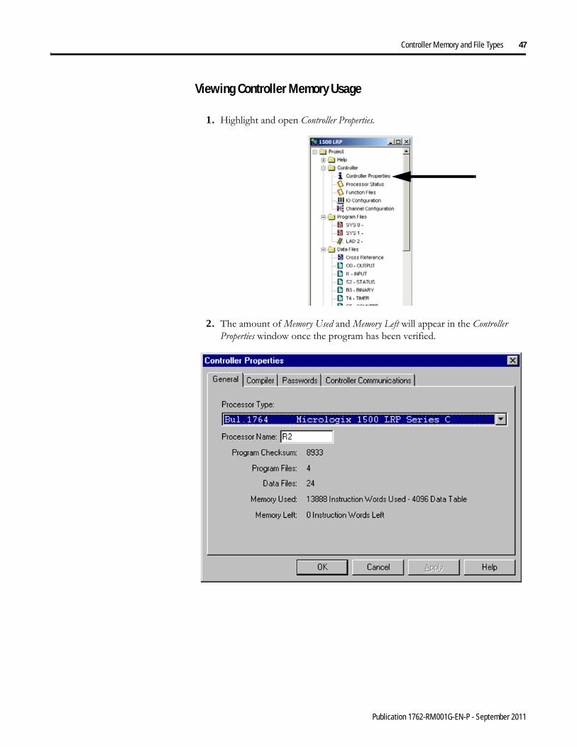
Controller Memory and File Types 47
Viewing Controller Memory Usage
1. Highlight and open Controller Properties.
2. The amount of Memory Used and Memory Left will appear in the Controller Properties window once the program has been verified.
Publication 1762-RM001G-EN-P - September 2011
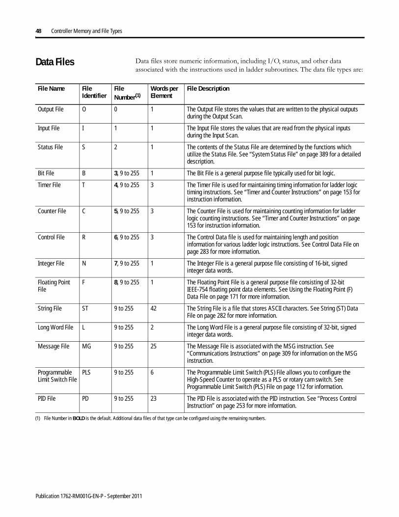
48 Controller Memory and File Types
Data Files Data files store numeric information, including I/O, status, and other data associated with the instructions used in ladder subroutines. The data file types are:
File Name File Identifier
File Number(1)
Words per Element
File Description
Output File O 0 1 The Output File stores the values that are written to the physical outputs during the Output Scan.
Input File I 1 1 The Input File stores the values that are read from the physical inputs during the Input Scan.
Status File S 2 1 The contents of the Status File are determined by the functions which utilize the Status File. See “System Status File” on page 389 for a detailed description.
Bit File B 3, 9 to 255 1 The Bit File is a general purpose file typically used for bit logic.
Timer File T 4, 9 to 255 3 The Timer File is used for maintaining timing information for ladder logic timing instructions. See “Timer and Counter Instructions” on page 153 for instruction information.
Counter File C 5, 9 to 255 3 The Counter File is used for maintaining counting information for ladder logic counting instructions. See “Timer and Counter Instructions” on page 153 for instruction information.
Control File R 6, 9 to 255 3 The Control Data file is used for maintaining length and position information for various ladder logic instructions. See Control Data File on page 283 for more information.
Integer File N 7, 9 to 255 1 The Integer File is a general purpose file consisting of 16-bit, signed integer data words.
Floating Point File
F 8, 9 to 255 1 The Floating Point File is a general purpose file consisting of 32-bit IEEE-754 floating point data elements. See Using the Floating Point (F) Data File on page 171 for more information.
String File ST 9 to 255 42 The String File is a file that stores ASCII characters. See String (ST) Data File on page 282 for more information.
Long Word File L 9 to 255 2 The Long Word File is a general purpose file consisting of 32-bit, signed integer data words.
Message File MG 9 to 255 25 The Message File is associated with the MSG instruction. See “Communications Instructions” on page 309 for information on the MSG instruction.
Programmable Limit Switch File
PLS 9 to 255 6 The Programmable Limit Switch (PLS) File allows you to configure the High-Speed Counter to operate as a PLS or rotary cam switch. See Programmable Limit Switch (PLS) File on page 112 for information.
PID File PD 9 to 255 23 The PID File is associated with the PID instruction. See “Process Control Instruction” on page 253 for more information.
(1) File Number in BOLD is the default. Additional data files of that type can be configured using the remaining numbers.
Publication 1762-RM001G-EN-P - September 2011

Controller Memory and File Types 49
Protecting Data Files During Download
Data File Download Protection
Once a user program is in the controller, there may be a need to update the ladder logic and download it to the controller without destroying user-configured variables in one or more data files in the controller. This situation can occur when an application needs to be updated, but the data that is relevant to the installation needs to remain intact.
This capability is referred to as Data File Download Protection. The protection feature operates when:
• A User Program is downloaded via programming software• A User Program is downloaded from a Memory Module
Setting Download File Protection
Download File Protection can be applied to the following data file types:
• Output (O)• Input (I)• Binary (B)• Timer (T)• Counter (C)• Control (R)• Integer (N)• Floating Point (F)• String (ST)• Long Word (L)• Proportional Integral Derivative (PD)• Message (MG)• Programmable Limit Switch (PLS)
TIP The data in the Status File cannot be protected.
Publication 1762-RM001G-EN-P - September 2011

50 Controller Memory and File Types
User Program Transfer Requirements
Data File Download Protection only operates when the following conditions are met during a User Program or Memory Module download to the controller:
• The controller contains protected data files.• The program being downloaded has the same number of protected data files
as the program currently in the controller.• All protected data file numbers, types, and sizes (number of elements)
currently in the controller exactly match that of the program being downloaded to the controller.
If all of these conditions are met, the controller will not write over any data file in the controller that is configured as Download Protected when a program is downloaded from a memory module or programming software.
If any of these conditions are not met, the entire User Program is transferred to the controller. Additionally, if the program in the controller contains protected files, the Data Protection Lost indicator (S:36/10) is set to indicate that protected data has been lost. For example, a control program with protected files is transferred to the controller. The original program did not have protected files or the files did not match. The data protection lost indicator (S:36/10) is then set. The data protection lost indicator represents that the protected files within the controller have had values downloaded and the user application may need to be re-configured.
Access the Download Data File Protect feature using RSLogix 500 programming software. For each data file you want protected, check the Memory Module/Download item within the protection box in the Data File Properties screen as shown in this illustration. To access this screen, right mouse click on the desired data file.
TIP The controller will not clear the Data Protection Lost indicator. It is up to the user to clear this bit.
Publication 1762-RM001G-EN-P - September 2011

Controller Memory and File Types 51
Static File Protection When a data file is Static File Protected, the values contained in it cannot be changed via communications, except during a program download to the controller.
Using Static File Protection with Data File Download Protection
Static File Protection and Data File Download Protection can be used in combination with any MicroLogix 1200 Controller Series B and higher, and MicroLogix 1500 Processor Series B and higher.
Setting Static File Protection
Static File Protection can be applied to the following data file types:
• Output (O)• Input (I)• Status (S)• Binary (B)• Timer (T)• Counter (C)• Control (R)• Integer (N)• Floating Point (F)• String (ST)• Long Word (L)• Proportional Integral Derivative (PD)• Message (MG)• Programmable Limit Switch (PLS)
Publication 1762-RM001G-EN-P - September 2011
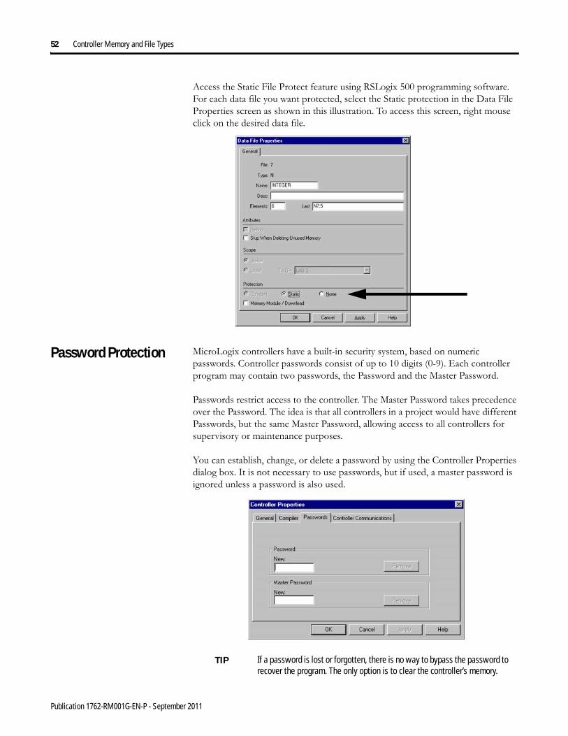
52 Controller Memory and File Types
Access the Static File Protect feature using RSLogix 500 programming software. For each data file you want protected, select the Static protection in the Data File Properties screen as shown in this illustration. To access this screen, right mouse click on the desired data file.
Password Protection MicroLogix controllers have a built-in security system, based on numeric passwords. Controller passwords consist of up to 10 digits (0-9). Each controller program may contain two passwords, the Password and the Master Password.
Passwords restrict access to the controller. The Master Password takes precedence over the Password. The idea is that all controllers in a project would have different Passwords, but the same Master Password, allowing access to all controllers for supervisory or maintenance purposes.
You can establish, change, or delete a password by using the Controller Properties dialog box. It is not necessary to use passwords, but if used, a master password is ignored unless a password is also used.
TIP If a password is lost or forgotten, there is no way to bypass the password to recover the program. The only option is to clear the controller’s memory.
Publication 1762-RM001G-EN-P - September 2011

Controller Memory and File Types 53
If the Memory Module User Program has the “Load Always” functionality enabled, and the controller User Program has a password specified, the controller compares the passwords before transferring the User Program from the Memory Module to the controller. If the passwords do not match, the User Program is not transferred and the program mismatch bit is set (S:5/9).
Clearing the Controller Memory
If you are locked out because you do not have the password for the controller, you can clear the controller memory and download a new User Program.
You can clear the memory when the programming software prompts you for a System or Master Password to go on-line with the controller. To do so:
1. Enter 65257636 (the telephone keypad equivalent of MLCLRMEM, MicroLogix Clear Memory).
2. When the Programming Software detects this number has been entered, it asks if you want to clear the memory in the controller.
3. If you reply “yes” to this prompt, the programming software instructs the controller to clear Program memory.
Allow Future Access Setting (OEM Lock)
The controller supports a feature which allows you to select if future access to the User Program should be allowed or disallowed after it has been transferred to the controller. This type of protection is particularly useful to an OEM (original equipment manufacturer) who develops an application and then distributes the application via a memory module or within a controller.
The Allow Future Access setting is found in the Controller Properties window as shown below.
Publication 1762-RM001G-EN-P - September 2011

54 Controller Memory and File Types
When Allow Future Access is deselected, the controller requires that the User Program in the controller is the same as the one in the programming device. If the programming device does not have a matching copy of the User Program, access to the User Program in the controller is denied. To access the User Program, clear controller memory and reload the program.
TIP Functions such as change mode, clear memory, restore program, and transfer memory module are allowed regardless of this selection.
Controller passwords are not associated with the Allow Future Access setting.
Publication 1762-RM001G-EN-P - September 2011

Chapter 3
Function Files
This chapter describes controller function files. The chapter is organized as follows:
• “Overview” on page 55• “Real-Time Clock Function File” on page 56• “Trim Pot Information Function File” on page 59• “Memory Module Information Function File” on page 60• “DAT Function File (MicroLogix 1500 only)” on page 63• “Base Hardware Information Function File” on page 66• “Communications Status File” on page 66• “Input/Output Status File” on page 79
Overview Function Files are one of the three primary file structures within the MicroLogix 1200 and MicroLogix 1500 controllers (Program Files and Data Files are the others). Function Files provide an efficient and logical interface to controller resources. Controller resources are resident (permanent) features such as the Real-Time Clock and High-Speed Counter. The features are available to the control program through either instructions that are dedicated to a specific function file, or via standard instructions such as MOV and ADD. The Function File types are:
Function FilesFile Name File
IdentifierFile Description
High-Speed Counter HSC This file type is associated with the High-Speed Counter function. See “Using the High-Speed Counter and Programmable Limit Switch” on page 87 for more information.
Pulse Train Output
(MicroLogix 1200 and 1500 BXB units only.)
PTO This file type is associated with the Pulse Train Output Instruction. See “Pulse Train Outputs (PTO) Function File” on page 123 for more information.
Pulse Width Modulation
(MicroLogix 1200 and 1500 BXB units only.)
PWM This file type is associated with the Pulse Width Modulation instruction. See “Pulse Width Modulation (PWM) Function File” on page 138 for more information.
Selectable Timed Interrupt STI This file type is associated with the Selectable Timed Interrupt function. See “Using the Selectable Timed Interrupt (STI) Function File” on page 242 for more information.
Event Input Interrupt EII This file type is associated with the Event Input Interrupt instruction. See “Using the Event Input Interrupt (EII) Function File” on page 247 for more information.
Real-Time Clock RTC This file type is associated with the Real-Time Clock (time of day) function. See “Real-Time Clock Function File” on page 56 for more information.
55 Publication 1762-RM001G-EN-P - September 2011

56 Function Files
Real-Time Clock Function File
The real-time clock provides year, month, day of month, day of week, hour, minute, and second information to the Real-Time Clock (RTC) Function File in the controller.
The Real-Time Clock parameters and their valid ranges are shown in the table below.
Trim Pot Information TPI This file type contains information about the Trim Pots. See “Trim Pot Information Function File” on page 59 for more information.
Memory Module Information
MMI This file type contains information about the Memory Module. See “Memory Module Information Function File” on page 60 for more information.
Data Access Tool Information
(MicroLogix 1500 only.)
DAT This file type contains information about the Data Access Tool. See “DAT Function File (MicroLogix 1500 only)” on page 63 for more information.
Base Hardware Information BHI This file type contains information about the controller’s hardware. See “Base Hardware Information Function File” on page 66 for the file structure.
Communications Status File
CS This file type contains information about the Communications with the controller. See “Communications Status File” on page 66 for the file structure.
I/O Status File IOS This file type contains information about the controller I/O. See “Input/Output Status File” on page 79 for the file structure.
Function FilesFile Name File
IdentifierFile Description
Real-Time Clock Function File
Feature Address Data Format Range Type User Program AccessYR - RTC Year RTC:0.YR word 1998 to 2097 status read-onlyMON - RTC Month RTC:0.MON word 1 to 12 status read-onlyDAY - RTC Day of Month RTC:0.DAY word 1 to 31 status read-onlyHR - RTC Hours RTC:0.HR word 0 to 23 (military time) status read-onlyMIN - RTC Minutes RTC:0.MIN word 0 to 59 status read-onlySEC - RTC Seconds RTC:0.SEC word 0 to 59 status read-onlyDOW - RTC Day of Week RTC:0.DOW word 0 to 6 (Sunday to Saturday) status read-onlyDS - Disabled RTC:0/DS binary 0 or 1 status read-onlyBL - RTC Battery Low RTC:0/BL binary 0 or 1 status read-only
Publication 1762-RM001G-EN-P - September 2011
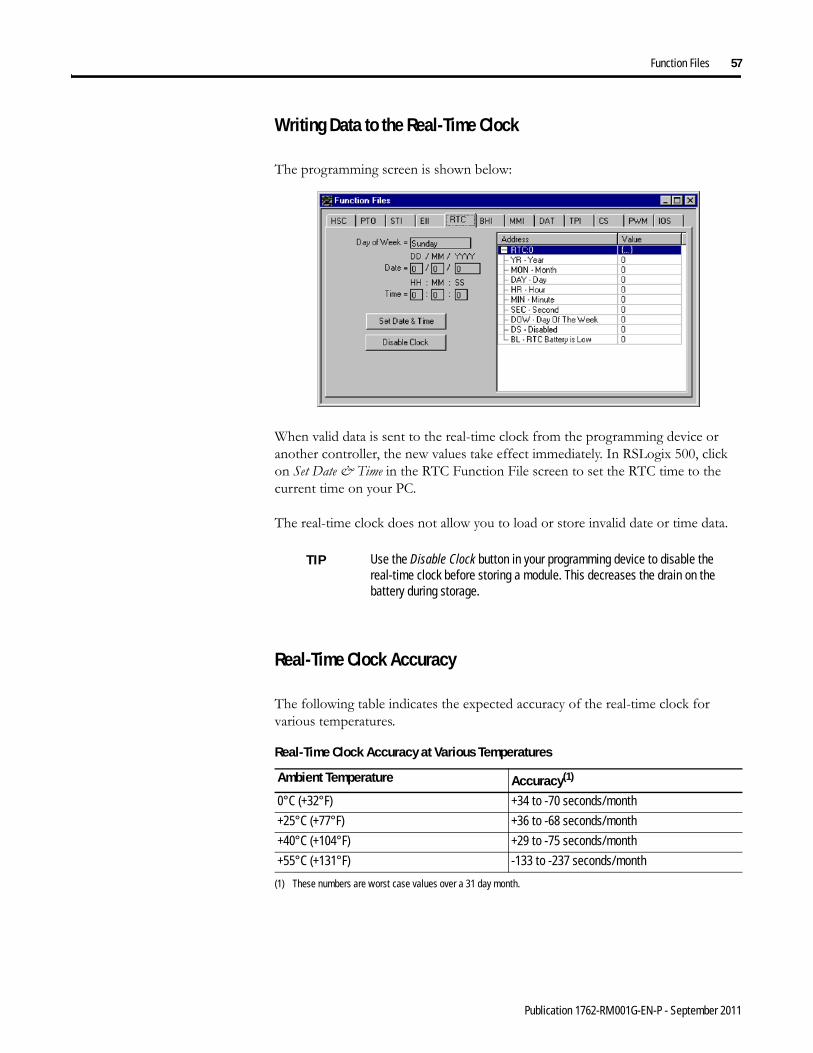
Function Files 57
Writing Data to the Real-Time Clock
The programming screen is shown below:
When valid data is sent to the real-time clock from the programming device or another controller, the new values take effect immediately. In RSLogix 500, click on Set Date & Time in the RTC Function File screen to set the RTC time to the current time on your PC.
The real-time clock does not allow you to load or store invalid date or time data.
Real-Time Clock Accuracy
The following table indicates the expected accuracy of the real-time clock for various temperatures.
TIP Use the Disable Clock button in your programming device to disable the real-time clock before storing a module. This decreases the drain on the battery during storage.
Real-Time Clock Accuracy at Various Temperatures
Ambient Temperature Accuracy(1)
(1) These numbers are worst case values over a 31 day month.
0°C (+32°F) +34 to -70 seconds/month
+25°C (+77°F) +36 to -68 seconds/month
+40°C (+104°F) +29 to -75 seconds/month
+55°C (+131°F) -133 to -237 seconds/month
Publication 1762-RM001G-EN-P - September 2011
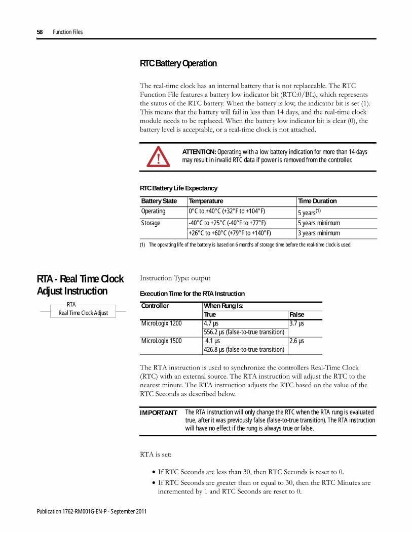
58 Function Files
RTC Battery Operation
The real-time clock has an internal battery that is not replaceable. The RTC Function File features a battery low indicator bit (RTC:0/BL), which represents the status of the RTC battery. When the battery is low, the indicator bit is set (1). This means that the battery will fail in less than 14 days, and the real-time clock module needs to be replaced. When the battery low indicator bit is clear (0), the battery level is acceptable, or a real-time clock is not attached.
RTA - Real Time Clock Adjust Instruction
Instruction Type: output
The RTA instruction is used to synchronize the controllers Real-Time Clock (RTC) with an external source. The RTA instruction will adjust the RTC to the nearest minute. The RTA instruction adjusts the RTC based on the value of the RTC Seconds as described below.
RTA is set:
• If RTC Seconds are less than 30, then RTC Seconds is reset to 0.• If RTC Seconds are greater than or equal to 30, then the RTC Minutes are
incremented by 1 and RTC Seconds are reset to 0.
ATTENTION: Operating with a low battery indication for more than 14 days may result in invalid RTC data if power is removed from the controller.
RTC Battery Life Expectancy
Battery State Temperature Time DurationOperating 0°C to +40°C (+32°F to +104°F) 5 years(1)
(1) The operating life of the battery is based on 6 months of storage time before the real-time clock is used.
Storage -40°C to +25°C (-40°F to +77°F) 5 years minimum
+26°C to +60°C (+79°F to +140°F) 3 years minimum
Execution Time for the RTA Instruction
Controller When Rung Is:True False
MicroLogix 1200 4.7 µs 3.7 µs556.2 µs (false-to-true transition)
MicroLogix 1500 4.1 µs 2.6 µs426.8 µs (false-to-true transition)
IMPORTANT The RTA instruction will only change the RTC when the RTA rung is evaluated true, after it was previously false (false-to-true transition). The RTA instruction will have no effect if the rung is always true or false.
RTAReal Time Clock Adjust
Publication 1762-RM001G-EN-P - September 2011

Function Files 59
The following conditions cause the RTA instruction to have no effect on the RTC data:
• No RTC attached to the controller• RTC is present, but disabled• An external (via communications) message to the RTC is in progress when
the RTA instruction is executed. (External communications to the RTC takes precedence over the RTA instruction.)
To re-activate the RTA instruction, the RTA rung must become false, and then true.
Trim Pot Information Function File
The composition of the Trim Pot Information (TPI) Function File is described below.
The data resident in TPI:0.POT0 represents the position of trim pot 0. The data resident in TPI:0.POT1 corresponds to the position of trim pot 1. The valid data range for both is from 0 (counterclockwise) to 250 (clockwise).
TIP There is only one internal storage bit allocated in the system for this instruction. Do not use more than one RTA instruction in your program.
TIP You can also use a MSG instruction to write RTC data from one controller to another to synchronize time. To send (write) RTC data, use RTC:0 as the source and the destination. This feature not available with the Series A controllers.
Trim Pot Function File
Data Address Data Format Range Type User Program Access
TPD Data O TPI:0.POT0 Word (16-bit integer)
0 - 250 Status Read Only
TPD Data 1 TPI:0.POT1 Word (16-bit integer)
0 - 250 Status Read Only
TP0 Error Code TPI:0.ER Word (bits 0 to 7) 0 - 3 Status Read Only
TP1 Error Code Word (bits 8 to 15)
Publication 1762-RM001G-EN-P - September 2011

60 Function Files
Error Conditions
If the controller detects a problem with either trim pot, the last values read remain in the data location, and an error code is put in the error code byte of the TPI file for whichever trim pot had the problem. Once the controller can access the trim pot hardware, the error code is cleared. The error codes are described in the table below.
Memory Module Information Function File
The controller has a Memory Module Information (MMI) File which is updated with data from the attached memory module. At power-up or on detection of a memory module being inserted, the catalog number, series, revision, and type (memory module and/or real-time clock) are identified and written to the MMI file in the user program. If a memory module and/or real-time clock is not attached, zeros are written to the MMI file.
The memory module function file programming screen is shown below:
Trim Pot Error Codes
Error Code Description0 Trim pot data is valid.
1 Trim pot subsystem detected, but data is invalid.
2 Trim pot subsystem did not initialize.
3 Trim pot subsystem failure.
Publication 1762-RM001G-EN-P - September 2011
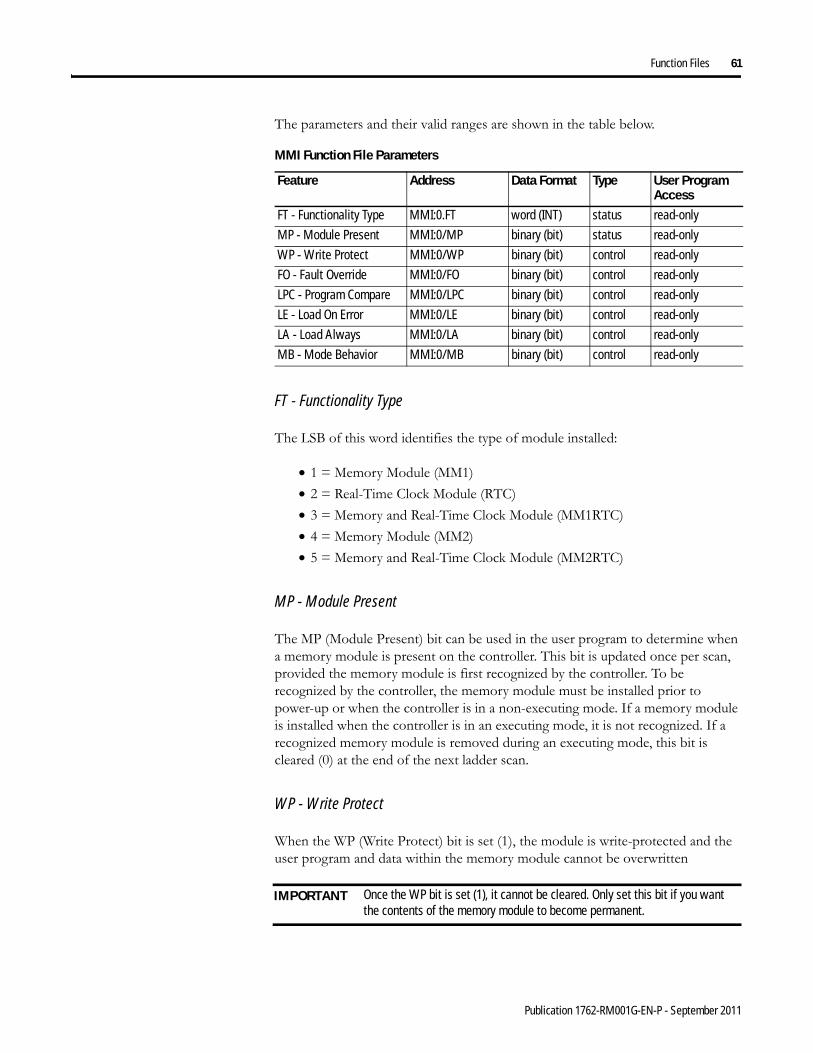
Function Files 61
The parameters and their valid ranges are shown in the table below.
FT - Functionality Type
The LSB of this word identifies the type of module installed:
• 1 = Memory Module (MM1)• 2 = Real-Time Clock Module (RTC)• 3 = Memory and Real-Time Clock Module (MM1RTC)• 4 = Memory Module (MM2)• 5 = Memory and Real-Time Clock Module (MM2RTC)
MP - Module Present
The MP (Module Present) bit can be used in the user program to determine when a memory module is present on the controller. This bit is updated once per scan, provided the memory module is first recognized by the controller. To be recognized by the controller, the memory module must be installed prior to power-up or when the controller is in a non-executing mode. If a memory module is installed when the controller is in an executing mode, it is not recognized. If a recognized memory module is removed during an executing mode, this bit is cleared (0) at the end of the next ladder scan.
WP - Write Protect
When the WP (Write Protect) bit is set (1), the module is write-protected and the user program and data within the memory module cannot be overwritten
MMI Function File Parameters
Feature Address Data Format Type User Program Access
FT - Functionality Type MMI:0.FT word (INT) status read-only
MP - Module Present MMI:0/MP binary (bit) status read-only
WP - Write Protect MMI:0/WP binary (bit) control read-only
FO - Fault Override MMI:0/FO binary (bit) control read-only
LPC - Program Compare MMI:0/LPC binary (bit) control read-only
LE - Load On Error MMI:0/LE binary (bit) control read-only
LA - Load Always MMI:0/LA binary (bit) control read-only
MB - Mode Behavior MMI:0/MB binary (bit) control read-only
IMPORTANT Once the WP bit is set (1), it cannot be cleared. Only set this bit if you want the contents of the memory module to become permanent.
Publication 1762-RM001G-EN-P - September 2011

62 Function Files
FO - Fault Override
The FO (Fault Override) bit represents the status of the fault override setting of the program stored in the memory module. It enables you to determine the value of the FO bit without actually loading the program from the memory module.
See “Fault Override At Power-Up” on page 392 for more information.
LPC - Load Program Compare
The LPC (Load Program Compare) bit shows the status of the load program compare selection in the memory module’s user program status file. It enables you to determine the value without actually loading the user program from the memory module.
See “Memory Module Program Compare” on page 396 for more information.
LE - Load on Error
The LE (Load on Error) bit represents the status of the load on error setting in the program stored in the memory module. It enables you to determine the value of the selection without actually loading the user program from the memory module.
See “Load Memory Module On Error Or Default Program” on page 393 for more information.
LA - Load Always
The LA (Load Always) bit represents the status of the load always setting in the program stored in the memory module. It enables you to determine the value of the selection without actually loading the user program from the memory module.
See “Load Memory Module Always” on page 393 for more information.
MB - Mode Behavior
The MB (Mode Behavior) bit represents the status of the mode behavior setting in the program stored in the memory module. It enables you to determine the value of the selection without actually loading the user program from the memory module.
See “Power-Up Mode Behavior” on page 393 for more information.
IMPORTANT The memory module fault override selection in the Memory Module Information (MMI) file does not determine the controller’s operation. It merely displays the setting of the user program’s Fault Override bit (S:1/8) in the memory module.
Publication 1762-RM001G-EN-P - September 2011
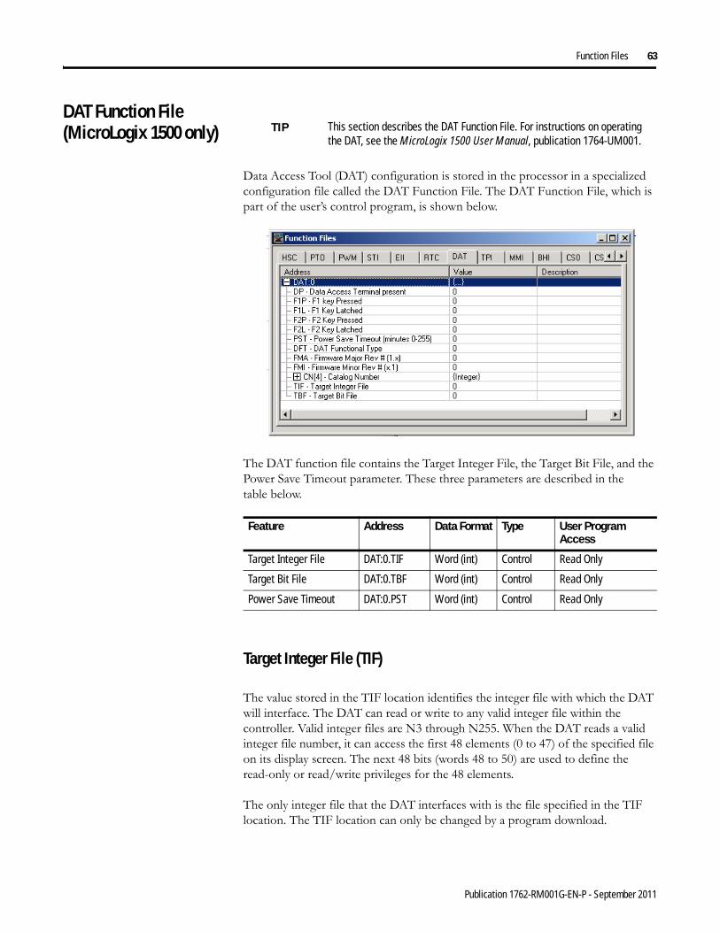
Function Files 63
DAT Function File (MicroLogix 1500 only)
Data Access Tool (DAT) configuration is stored in the processor in a specialized configuration file called the DAT Function File. The DAT Function File, which is part of the user’s control program, is shown below.
The DAT function file contains the Target Integer File, the Target Bit File, and the Power Save Timeout parameter. These three parameters are described in the table below.
Target Integer File (TIF)
The value stored in the TIF location identifies the integer file with which the DAT will interface. The DAT can read or write to any valid integer file within the controller. Valid integer files are N3 through N255. When the DAT reads a valid integer file number, it can access the first 48 elements (0 to 47) of the specified file on its display screen. The next 48 bits (words 48 to 50) are used to define the read-only or read/write privileges for the 48 elements.
The only integer file that the DAT interfaces with is the file specified in the TIF location. The TIF location can only be changed by a program download.
TIP This section describes the DAT Function File. For instructions on operating the DAT, see the MicroLogix 1500 User Manual, publication 1764-UM001.
Feature Address Data Format Type User Program Access
Target Integer File DAT:0.TIF Word (int) Control Read Only
Target Bit File DAT:0.TBF Word (int) Control Read Only
Power Save Timeout DAT:0.PST Word (int) Control Read Only
Publication 1762-RM001G-EN-P - September 2011
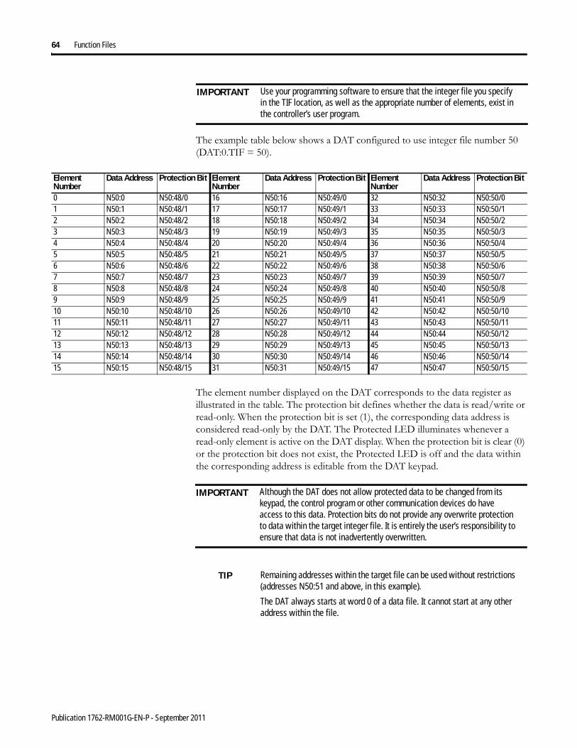
64 Function Files
The example table below shows a DAT configured to use integer file number 50 (DAT:0.TIF = 50).
The element number displayed on the DAT corresponds to the data register as illustrated in the table. The protection bit defines whether the data is read/write or read-only. When the protection bit is set (1), the corresponding data address is considered read-only by the DAT. The Protected LED illuminates whenever a read-only element is active on the DAT display. When the protection bit is clear (0) or the protection bit does not exist, the Protected LED is off and the data within the corresponding address is editable from the DAT keypad.
IMPORTANT Use your programming software to ensure that the integer file you specify in the TIF location, as well as the appropriate number of elements, exist in the controller’s user program.
Element Number
Data Address Protection Bit Element Number
Data Address Protection Bit Element Number
Data Address Protection Bit
0 N50:0 N50:48/0 16 N50:16 N50:49/0 32 N50:32 N50:50/01 N50:1 N50:48/1 17 N50:17 N50:49/1 33 N50:33 N50:50/12 N50:2 N50:48/2 18 N50:18 N50:49/2 34 N50:34 N50:50/23 N50:3 N50:48/3 19 N50:19 N50:49/3 35 N50:35 N50:50/34 N50:4 N50:48/4 20 N50:20 N50:49/4 36 N50:36 N50:50/45 N50:5 N50:48/5 21 N50:21 N50:49/5 37 N50:37 N50:50/56 N50:6 N50:48/6 22 N50:22 N50:49/6 38 N50:38 N50:50/67 N50:7 N50:48/7 23 N50:23 N50:49/7 39 N50:39 N50:50/78 N50:8 N50:48/8 24 N50:24 N50:49/8 40 N50:40 N50:50/89 N50:9 N50:48/9 25 N50:25 N50:49/9 41 N50:41 N50:50/910 N50:10 N50:48/10 26 N50:26 N50:49/10 42 N50:42 N50:50/1011 N50:11 N50:48/11 27 N50:27 N50:49/11 43 N50:43 N50:50/1112 N50:12 N50:48/12 28 N50:28 N50:49/12 44 N50:44 N50:50/1213 N50:13 N50:48/13 29 N50:29 N50:49/13 45 N50:45 N50:50/1314 N50:14 N50:48/14 30 N50:30 N50:49/14 46 N50:46 N50:50/1415 N50:15 N50:48/15 31 N50:31 N50:49/15 47 N50:47 N50:50/15
IMPORTANT Although the DAT does not allow protected data to be changed from its keypad, the control program or other communication devices do have access to this data. Protection bits do not provide any overwrite protection to data within the target integer file. It is entirely the user’s responsibility to ensure that data is not inadvertently overwritten.
TIP Remaining addresses within the target file can be used without restrictions (addresses N50:51 and above, in this example).
The DAT always starts at word 0 of a data file. It cannot start at any other address within the file.
Publication 1762-RM001G-EN-P - September 2011
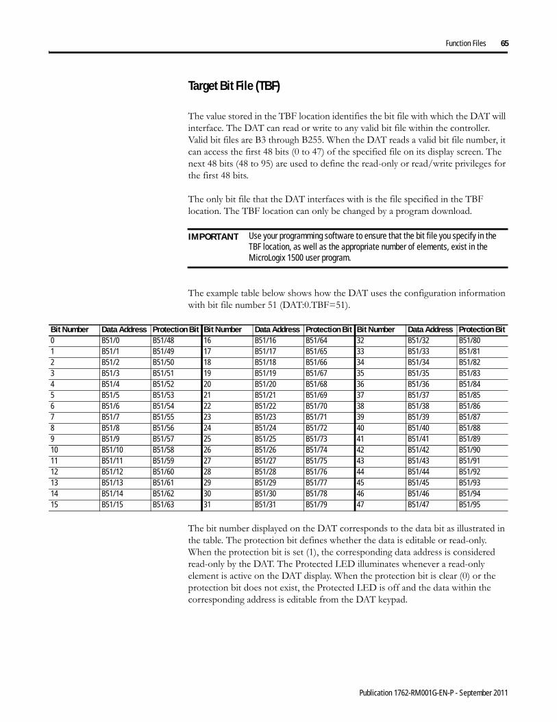
Function Files 65
Target Bit File (TBF)
The value stored in the TBF location identifies the bit file with which the DAT will interface. The DAT can read or write to any valid bit file within the controller. Valid bit files are B3 through B255. When the DAT reads a valid bit file number, it can access the first 48 bits (0 to 47) of the specified file on its display screen. The next 48 bits (48 to 95) are used to define the read-only or read/write privileges for the first 48 bits.
The only bit file that the DAT interfaces with is the file specified in the TBF location. The TBF location can only be changed by a program download.
The example table below shows how the DAT uses the configuration information with bit file number 51 (DAT:0.TBF=51).
The bit number displayed on the DAT corresponds to the data bit as illustrated in the table. The protection bit defines whether the data is editable or read-only. When the protection bit is set (1), the corresponding data address is considered read-only by the DAT. The Protected LED illuminates whenever a read-only element is active on the DAT display. When the protection bit is clear (0) or the protection bit does not exist, the Protected LED is off and the data within the corresponding address is editable from the DAT keypad.
IMPORTANT Use your programming software to ensure that the bit file you specify in the TBF location, as well as the appropriate number of elements, exist in the MicroLogix 1500 user program.
Bit Number Data Address Protection Bit Bit Number Data Address Protection Bit Bit Number Data Address Protection Bit0 B51/0 B51/48 16 B51/16 B51/64 32 B51/32 B51/801 B51/1 B51/49 17 B51/17 B51/65 33 B51/33 B51/812 B51/2 B51/50 18 B51/18 B51/66 34 B51/34 B51/823 B51/3 B51/51 19 B51/19 B51/67 35 B51/35 B51/834 B51/4 B51/52 20 B51/20 B51/68 36 B51/36 B51/845 B51/5 B51/53 21 B51/21 B51/69 37 B51/37 B51/856 B51/6 B51/54 22 B51/22 B51/70 38 B51/38 B51/867 B51/7 B51/55 23 B51/23 B51/71 39 B51/39 B51/878 B51/8 B51/56 24 B51/24 B51/72 40 B51/40 B51/889 B51/9 B51/57 25 B51/25 B51/73 41 B51/41 B51/8910 B51/10 B51/58 26 B51/26 B51/74 42 B51/42 B51/9011 B51/11 B51/59 27 B51/27 B51/75 43 B51/43 B51/9112 B51/12 B51/60 28 B51/28 B51/76 44 B51/44 B51/9213 B51/13 B51/61 29 B51/29 B51/77 45 B51/45 B51/9314 B51/14 B51/62 30 B51/30 B51/78 46 B51/46 B51/9415 B51/15 B51/63 31 B51/31 B51/79 47 B51/47 B51/95
Publication 1762-RM001G-EN-P - September 2011
66 Function Files
Base Hardware Information Function File
The base hardware information (BHI) file is a read-only file that contains a description of the MicroLogix 1200 Controller or the MicroLogix 1500 Base Unit.
Communications Status File
The Communications Status (CS) File is a read-only file that contains information on how the controller communication parameters are configured and status information on communications activity.
The communications status file uses:
There is one Communications Status File for each communications port. Communications Status File CS0 corresponds to Channel 0 on the controller. Communications Status File CS1 corresponds to Channel 1 on the 1764-LRP processor.
IMPORTANT Although the DAT does not allow protected data to be changed from its keypad, the control program or other communication devices do have access to this data. Protection bits do not provide any overwrite protection to data within the target bit file. It is entirely the user’s responsibility to ensure that data is not inadvertently overwritten.
TIP Remaining addresses within the target file can be used without restrictions (addresses B51/96 and above, in this example).
The DAT always starts at bit 0 of a data file. It cannot start at any other address within the file.
Base Hardware Information Function File (BHI)
Address DescriptionBHI:0.CN CN - Catalog Number
BHI:0.SRS SRS - Series
BHI:0.REV REV - Revision
BHI:0.FT FT - Functionality Type
Communications Status File Size
Controller Number of Word ElementsMicroLogix 1500 1764-LSP Series A Processor 44 1-word elements
MicroLogix 1200
MicroLogix 1500 1764-LSP Series B and 1764-LRP Processors
71 1-word elements
TIP You can use the Communications Status File information as a troubleshooting tool for communications issues.
Publication 1762-RM001G-EN-P - September 2011

Function Files 67
The data file is structured as:
The following tables show the details of each block in the Communications Status File.
General Status Block of Communications Status File
Communications Status File
Word Description Applies to Controller Details on Page
0 to 5 General Channel Status Block MicroLogix 1200 and 1500 67
6 to 22 DLL Diagnostic Counters Block MicroLogix 1200 and 1500 69
23 to 42 DLL Active Node Table Block MicroLogix 1200 and 1500 78
words 43 to 70 when using DF1 Full-Duplex, DF1 Half-Duplex, DH-485, or ASCII (1):
(1) ASCII can only be used with the MicroLogix 1200 and MicroLogix 1500 1764-LSP Series B (and higher) and 1764-LRP Processors.
43 End of List Category Identifier Code (always 0)
MicroLogix 1200 and 1500 --
43 to 70 Reserved • MicroLogix 1200
• MicroLogix 1500 1764-LSP Series B and 1764-LRP Processors
--
words 43 to 70 when using Modbus RTU Slave:
43 to 69 Modbus Slave Diagnostic Counters Block • MicroLogix 1200
• MicroLogix 1500 1764-LSP Series B and 1764-LRP Processors
74
70 End of List Category Identifier Code (always 0)
• MicroLogix 1200
• MicroLogix 1500 1764-LSP Series B and 1764-LRP Processors
--
General Channel Status Block
Word Bit Description0 - Communications Channel General Status Information Category Identifier
Code
1 - Length
2 - Format Code
3 - Communications Configuration Error Code
Publication 1762-RM001G-EN-P - September 2011

68 Function Files
Diagnostic Counter Block of Communications Status File
With RSLogix 500 version 6.10.10 and later, formatted displays of the diagnostic counters for each configured channel are available under Channel Status. These displays include a Clear button that allows you to reset the diagnostic counters while monitoring them online with the programming software.
4 0 ICP – Incoming Command Pending Bit
This bit is set (1) when the controller determines that another device has requested information from this controller. Once the request has been satisfied, the bit is cleared (0).
1 MRP – Incoming Message Reply Pending Bit
This bit is set (1) when the controller determines that another device has supplied the information requested by a MSG instruction executed by this controller. When the appropriate MSG instruction is serviced (during end-of-scan, SVC, or REF), this bit is cleared (0).
2 MCP – Outgoing Message Command Pending Bit
This bit is set (1) when the controller has one or more MSG instructions enabled and in the communication queue. This bit is cleared (0) when the queue is empty.
3 SSB – Selection Status Bit
This bit indicates that the controller is in the System Mode. It is always set.
4 CAB – Communications Active Bit
This bit is set (1) when at least one other device is on the DH-485 network. If no other devices are on the network, this bit is cleared (0).
5 to 14 Reserved
15 Communications Toggle Push Button Communications Defaults Active. This bit is set (1) whenever Channel 0 is in the default communications mode. The bit is cleared (0) when Channel 0 is in user configured communications mode. (Always 0 for 1764-LRP Processor Channel 1) This bit is not available with the Series A controllers.
5 0 to 7 Node Address - This byte value contains the node address of your controller on the network.
8 to 15 Baud Rate - This byte value contains the baud rate of the controller on the network.
General Channel Status Block
Publication 1762-RM001G-EN-P - September 2011

Function Files 69
Diagnostic Counter Blocks are shown for:
• DH-485 ( on page 69)• DF1 Full-Duplex ( on page 70)• DF1 Half-Duplex Slave ( on page 71)• DF1 Half-Duplex Master ( on page 72)• DF1 Radio Modem ( on page 73)• Modbus RTU Slave ( on page 74)• Modbus RTU Master ( on page 76)• ASCII ( on page 77)
TIP For the MicroLogix 1500 LRP with OS Series C, FRN 8, and higher, clicking on the Clear button while online monitoring Channel Status of either channel 0 or channel 1 will reset all of the channel status diagnostic counters for both channels to zero.
Prior to OS Series C, FRN 8, the only channel status diagnostic counters that are reset when the Clear button is clicked are the ones on the channel that the programming terminal is connected through. For instance, if your programming terminal is connected online via channel 0 and you are monitoring the Channel Status of channel 1, when you click on the Clear button, only the channel 0 diagnostic counters will be reset - the channel 1 diagnostic counters will not be reset.
DH-485 Diagnostic Counters Block
Word Bit Description6 - Diagnostic Counters Category Identifier Code (always 2)
7 - Length (always 30)
8 - Format Code (always 0)
9 - Total Message Packets Received
10 - Total Message Packets Sent
11 0 to 7 Message Packet Retries
8 to 15 Retry Limit Exceeded (Non-Delivery)
12 0 to 7 NAK – No Memories Sent
8 to 15 NAK – No Memories Received
13 0 to 7 Total Bad Message Packets Received
8 to 15 Reserved
14 to 22 - Reserved
Publication 1762-RM001G-EN-P - September 2011

70 Function Files
DF1 Full-Duplex Diagnostic Counters Block
Word Bit Description6 - Diagnostic Counters Category Identifier Code (always 2)
7 - Length (always 30)
8 - Format Code (always 1)
9 0 CTS
1 RTS
2 Reserved
3 Channel 0 - Reserved, Channel 1 - DCD
4 to 15 Reserved
10 - Total Message Packets Sent
11 - Total Message Packets Received
12 - Undelivered Message Packets
13 - ENQuiry Packets Sent
14 - NAK Packets Received
15 - ENQuiry Packets Received
16 - Bad Message Packets Received and NAKed
17 - No Buffer Space and NAK’ed
18 - Duplicate Message Packets Received
19 to 22 - Reserved
Publication 1762-RM001G-EN-P - September 2011

Function Files 71
DF1 Half-Duplex Slave Diagnostic Counters Block
Word Bit Description6 - Diagnostic Counters Category Identifier Code (always 2)
7 - Length (always 30)
8 - Format Code (always 2)
9 0 CTS
1 RTS
2 Reserved
3 Channel 0 - Reserved, Channel 1 - DCD
4 to 15 Reserved
10 - Total Message Packets Sent
11 - Total Message Packets Received
12 - Undelivered Message Packets
13 - Message Packets Retried
14 - NAK Packets Received
15 - Polls Received
16 - Bad Message Packets Received
17 - No Buffer Space
18 - Duplicate Message Packets Received
19 to 22 - Reserved
Publication 1762-RM001G-EN-P - September 2011

72 Function Files
DF1 Half-Duplex Master Diagnostic Counters Block(MicroLogix 1200, FRN 7 and higherMicroLogix 1500 1764-LSP, FRN 8 and higherMicroLogix 1500 1764-LRP, FRN 8 and higher [Channel 1 only])
Word Bit Description6 - Diagnostic Counters Category Identifier Code (always 2)
7 - Length (always 30)
8 - Format Code (always 3)
9 0 CTS
1 RTS
2 Reserved
3 Channel 0 - Reserved, Channel 1 - DCD
4 to 15 Reserved
10 - Total Message Packets Sent
11 - Total Message Packets Received
12 - Undelivered Message Packets
13 - Message Packets Retried
14 - Reserved
15 - Polls Sent
16 - Bad Message Packets Received
17 - No Buffer Space, Received Packet Dropped
18 - Duplicate Message Packets Received
19 - Last Normal Poll List Scan
20 - Max. Normal Poll List Scan
21 - Last Priority Poll List Scan
22 - Max. Priority Poll List Scan
Publication 1762-RM001G-EN-P - September 2011

Function Files 73
DF1 Radio Modem Diagnostic Counters Block(MicroLogix 1200, FRN 7 and higherMicroLogix 1500 1764-LSP, FRN 8 and higherMicroLogix 1500 1764-LRP, FRN 8 and higher [Channel 1 only]
Word Bit Description6 - Diagnostic Counters Category Identifier Code (always 2)
7 - Length (always 30)
8 - Format Code (always 1)
9 0 CTS
1 RTS
2 Reserved
3 Channel 0 - Reserved, Channel 1 - DCD
4 to 15 Reserved
10 - Total Message Packets Sent
11 - Total Message Packets Received
12 - Undelivered Message Packets
13 to 15 - Reserved
16 - Bad Message Packets Received
17 - No Buffer Space, Received Packet Dropped
18 - Duplicate Message Packets Received
19 to 22 - Reserved
Publication 1762-RM001G-EN-P - September 2011

74 Function Files
Modbus RTU Slave Diagnostic Counters Block (Data Link Layer)(MicroLogix 1200 Controllers, and MicroLogix 1500 1764-LSP Series B and 1764-LRP Processors)
Word Bit Description6 - Diagnostic Counters Category Identifier Code (always 2)
7 - Length (always 30)
8 - Format Code (always 4)
9 0 CTS
1 RTS
2 Reserved
3 Channel 0 - Reserved, Channel 1 - DCD
4 to 15 Reserved
10 - Total Message Packets Sent
11 - Total Message Packets Received for This Slave
12 - Total Message Packets Received
13 - Link Layer Error Count
14 - Link Layer Error Code
15 to 22 - Reserved
Modbus RTU Slave Diagnostic Counters Block (Presentation Layer) (MicroLogix 1200 Controllers, and MicroLogix 1500 1764-LSP Series B and 1764-LRP Processors)
Word Bit Description43 - Diagnostic Counters Category Identifier Code (always 10)44 - Length (always 14)45 - Format Code (always 0)46 - Pre-Send Time Delay47 0 to 7 Node Address
8 to 15 Reserved48 - Inter-Character Timeout49 - RTS Send Delay
Publication 1762-RM001G-EN-P - September 2011

Function Files 75
50 - RTS Off Delay51 0 to 7 Baud Rate
8 and 9 Parity10 to 15 Reserved
52 - Diagnostic Counters Category Identifier Code (always 6)53 - Length (always 32)54 - Format Code (always 0)55 - Presentation Layer Error Code56 - Presentation Layer Error Count57 - Execution Function Error Code58 - Last Transmitted Exception Code59 - Data File Number of Error Request60 - Element Number of Error Request61 - Function Code 1 Message Counter62 - Function Code 2 Message Counter63 - Function Code 3 Message Counter64 - Function Code 4 Message Counter65 - Function Code 5 Message Counter66 - Function Code 6 Message Counter67 - Function Code 8 Message Counter68 - Function Code 15 Message Counter69 - Function Code 16 Message Counter
Modbus RTU Slave Diagnostic Counters Block (Presentation Layer) (MicroLogix 1200 Controllers, and MicroLogix 1500 1764-LSP Series B and 1764-LRP Processors)
Word Bit Description
Publication 1762-RM001G-EN-P - September 2011

76 Function Files
Modbus RTU Master Diagnostic Counters Block (Data Link Layer)(MicroLogix 1200, FRN 8 and higherMicroLogix 1500 1764-LSP, FRN 9 and higherMicroLogix 1500 1764-LRP, FRN 9 and higher)
Word Bit Description6 - Diagnostic Counters Category Identifier Code (always 2)
7 - Length (always 30)
8 - Format Code (always 9)
9 0 CTS
1 RTS
2 Reserved
3 Channel 0 - Reserved, Channel 1 - DCD
4 to 15 Reserved
10 - Total Message Packets Sent
11 - Reserved
12 - Total Message Packets Received
13 - Link Layer Error Count
14 - Link Layer Error Code
15 to 22 - Reserved
Modbus RTU Master Diagnostic Counters Block (Presentation Layer)(MicroLogix 1200, FRN 8 and higherMicroLogix 1500 1764-LSP, FRN 9 and higherMicroLogix 1500 1764-LRP, FRN 9 and higher)
Word Bit Description52 - Diagnostic Counters Category Identifier Code (always 6)53 - Length (always 32)54 - Format Code (always 0)55 - ERR 1: Illegal Function56 - Last Device Reporting ERR 157 - ERR 2: Illegal Data Address58 - Last Device Reporting ERR 259 - ERR 3: Illegal Data Value60 - Last Device Reporting ERR 361 - ERR 4: Slave Device Failure62 - ERR 5: Acknowledge63 - ERR 6: Slave Device Busy64 - ERR 7: Negative Acknowledgement65 - ERR 8: Memory Parity Error66 - Non-Standard Response67 - Last Device Reporting ERR 4 to ERR 8 or Non-Standard Response68 and 69 - Reserved (always 0)
Publication 1762-RM001G-EN-P - September 2011

Function Files 77
ASCII Diagnostic Counters Block(MicroLogix 1200 Series B Controllers, and MicroLogix 1500 1764-LSP Series B and 1764-LRP Processors)
Word Bit Description6 - DLL Diagnostic Counters Category Identifier code (always 2)
7 - Length (always 30)
8 - Format Code (always 5)
9 0 CTS
1 RTS
2 Reserved
3 Channel 0 - Reserved, Channel 1 - DCD
4 to 15 Reserved
10 0 Software Handshaking Status
1 to 15 Reserved
11 - Echo Character Count
12 - Received Character Count
13 to 18 - Reserved
19 - Bad Character Count
20 to 22 - Reserved
Publication 1762-RM001G-EN-P - September 2011
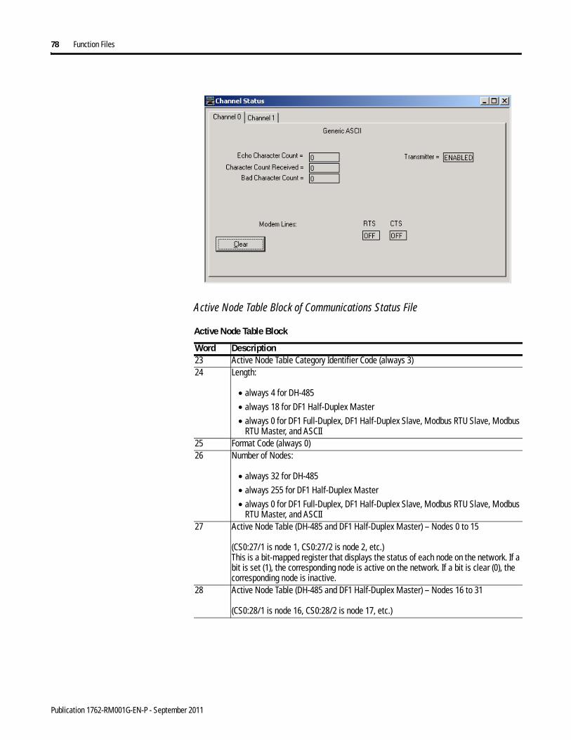
78 Function Files
Active Node Table Block of Communications Status File
Active Node Table Block
Word Description23 Active Node Table Category Identifier Code (always 3)24 Length:
• always 4 for DH-485
• always 18 for DF1 Half-Duplex Master
• always 0 for DF1 Full-Duplex, DF1 Half-Duplex Slave, Modbus RTU Slave, Modbus RTU Master, and ASCII
25 Format Code (always 0)26 Number of Nodes:
• always 32 for DH-485
• always 255 for DF1 Half-Duplex Master
• always 0 for DF1 Full-Duplex, DF1 Half-Duplex Slave, Modbus RTU Slave, Modbus RTU Master, and ASCII
27 Active Node Table (DH-485 and DF1 Half-Duplex Master) – Nodes 0 to 15
(CS0:27/1 is node 1, CS0:27/2 is node 2, etc.)This is a bit-mapped register that displays the status of each node on the network. If a bit is set (1), the corresponding node is active on the network. If a bit is clear (0), the corresponding node is inactive.
28 Active Node Table (DH-485 and DF1 Half-Duplex Master) – Nodes 16 to 31
(CS0:28/1 is node 16, CS0:28/2 is node 17, etc.)
Publication 1762-RM001G-EN-P - September 2011

Function Files 79
If you are using RSLogix 500 version 6.10.10 or higher, you can view the active node table by clicking on “Processor Status” and then selecting the tab for the configured channel.
Input/Output Status File The input/output status (IOS) file is a read-only file in the controller that contains information on the status of the embedded and local expansion I/O. The data file is structured as:
29 Active Node Table (DF1 Half-Duplex Master) – Nodes 32 to 47
(CS0:29/1 is node 32, CS0:29/2 is node 33, etc.)
…
42 Active Node Table (DF1 Half-Duplex Master) – Nodes 240 to 255
(CS0:42/1 is node 240, CS0:42/2 is node 241, etc.)
Active Node Table Block
I/O Status File
Word Description0 Embedded Module Error Code – Always zero
1 to 6 Expansion Module Error Code – The word number corresponds to the module’s slot number. Refer to the I/O module’s documentation for specific information. (MicroLogix 1200)
1 to 16(1) Expansion Module Error Code – The word number corresponds to the module’s slot number. Refer to the I/O module’s documentation for specific information. (MicroLogix 1500)
(1) 1 to 8 for Series A Base Units.
Publication 1762-RM001G-EN-P - September 2011

80 Function Files
Notes:
Publication 1762-RM001G-EN-P - September 2011

Chapter 4
Programming Instructions Overview
Instruction Set The following table shows the MicroLogix 1200 and 1500 programming instructions listed within their functional group.(1)
(1) The RTA - Real Time Clock Adjust Instruction appears on page 58 following the Real-Time Clock Function File information.
Functional Group Description PageHigh-Speed Counter HSL, RAC – The high-speed counter instructions (along with the HSC function file) allow you to monitor
and control the high-speed outputs. Generally used with DC inputs.87
High-Speed Outputs PTO, PWM – The high-speed output instructions (along with the PTO and PWM function files) allow you to monitor and control the high-speed outputs. Generally used with FET outputs (BXB units).
119
Relay-Type (Bit) XIC, XIO, OTE, OTL, OTU, OSR, ONS, OSF – The relay-type (bit) instructions monitor and control the status of bits.
147
Timer and Counter TON, TOF, RTO, CTU, CTD, RES – The timer and counter instructions control operations based on time or the number of events.
153
Compare EQU, NEQ, LES, LEQ, GRT, GEQ, MEQ, LIM – The compare instructions compare values by using a specific compare operation.
163
Math ADD, SUB, MUL, DIV, NEG, CLR, ABS, SQR, SCL, SCP, SWP – The math instructions perform arithmetic operations.
169
Conversion DCD, ENC, TOD, FRD, GCD – The conversion instructions multiplex and de-multiplex data and perform conversions between binary and decimal values.
181
Logical AND, OR, XOR, NOT – The logical instructions perform bit-wise logical operations on words. 191
Move MOV, MVM – The move instructions modify and move words. 195
File CPW, COP, FLL, BSL, BSR, FFL, FFU, LFL, LFU – The file instructions perform operations on file data. 199
Sequencer SQC, SQO, SQL – Sequencer instructions are used to control automatic assembly machines that have consistent and repeatable operations.
215
Program Control JMP, LBL, JSR, SBR, RET, SUS, TND, MCR, END – The program flow instructions change the flow of ladder program execution.
223
Input and Output IIM, IOM, REF – The input and output instructions allow you to selectively update data without waiting for the input and output scans.
229
User Interrupt STS, INT, UID, UIE, UIF – The user interrupt instructions allow you to interrupt your program based on defined events.
233
Process Control PID – The process control instruction provides closed-loop control. 253
ASCII ABL, ACB, ACI, ACL, ACN, AEX, AHL, AIC, ARD, ARL, ASC, ASR, AWA, AWT – The ASCII instructions convert and write ASCII strings. They cannot be used with MicroLogix 1500 1764-LSP Series A processors.
279
Communications MSG, SVC – The communication instructions read or write data to another station. 309
Recipe(MicroLogix 1500 only)
RCP – The recipe instruction allows you to transfer a data set between the recipe database and a set of user-specified data table elements.
359
Data Logging(MicroLogix 1500 1764-LRP only)
DLG – The data logging instruction allow you to capture time-stamped and date-stamped data. 359
81 Publication 1762-RM001G-EN-P - September 2011
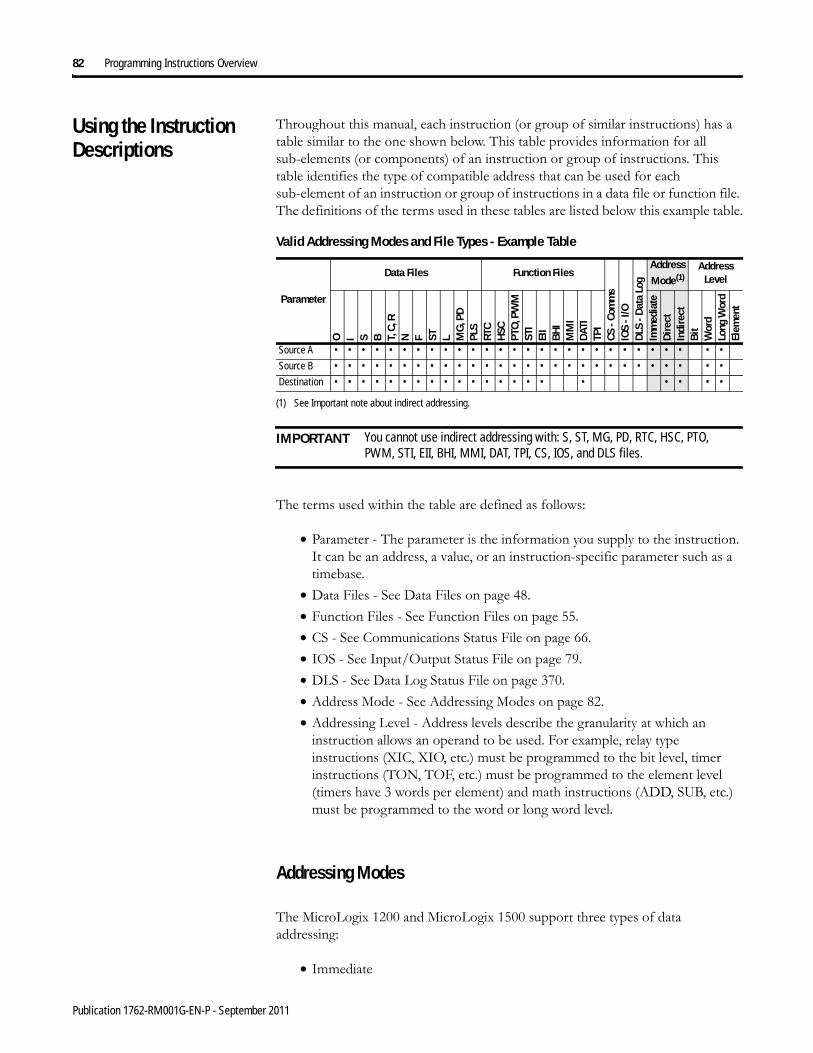
82 Programming Instructions Overview
Using the Instruction Descriptions
Throughout this manual, each instruction (or group of similar instructions) has a table similar to the one shown below. This table provides information for all sub-elements (or components) of an instruction or group of instructions. This table identifies the type of compatible address that can be used for each sub-element of an instruction or group of instructions in a data file or function file. The definitions of the terms used in these tables are listed below this example table.
The terms used within the table are defined as follows:
• Parameter - The parameter is the information you supply to the instruction. It can be an address, a value, or an instruction-specific parameter such as a timebase.
• Data Files - See Data Files on page 48.• Function Files - See Function Files on page 55.• CS - See Communications Status File on page 66.• IOS - See Input/Output Status File on page 79.• DLS - See Data Log Status File on page 370.• Address Mode - See Addressing Modes on page 82.• Addressing Level - Address levels describe the granularity at which an
instruction allows an operand to be used. For example, relay type instructions (XIC, XIO, etc.) must be programmed to the bit level, timer instructions (TON, TOF, etc.) must be programmed to the element level (timers have 3 words per element) and math instructions (ADD, SUB, etc.) must be programmed to the word or long word level.
Addressing Modes
The MicroLogix 1200 and MicroLogix 1500 support three types of data addressing:
• Immediate
Valid Addressing Modes and File Types - Example Table
Parameter
Data Files Function Files
CS -
Com
ms
IOS
- I/O
DLS
- D
ata
Log
Address Mode(1)
(1) See Important note about indirect addressing.
Address Level
O I S B T, C
, RN F ST L M
G, P
DPL
SRT
CH
SCPT
O, P
WM
STI
EII
BHI
MM
IDA
TITP
I
Imm
edia
teD
irec
tIn
dire
ctB
itW
ord
Long
Wor
dEl
emen
t
Source A • • • • • • • • • • • • • • • • • • • • • • • • • • • •
Source B • • • • • • • • • • • • • • • • • • • • • • • • • • • •
Destination • • • • • • • • • • • • • • • • • • • • •
IMPORTANT You cannot use indirect addressing with: S, ST, MG, PD, RTC, HSC, PTO, PWM, STI, EII, BHI, MMI, DAT, TPI, CS, IOS, and DLS files.
Publication 1762-RM001G-EN-P - September 2011
Programming Instructions Overview 83
• Direct• Indirect
The MicroLogix 1200 and 1500 do not support indexed addressing. Indexed addressing can be duplicated with indirect addressing. See Example - Using Indirect Addressing to Duplicate Indexed Addressing on page 85.
How or when each type is used depends on the instruction being programmed and the type of elements specified within the operands of the instruction. By supporting these three addressing methods, the MicroLogix 1200 and 1500 allow incredible flexibility in how data can be monitored or manipulated. Each of the addressing modes are described below.
Immediate Addressing
Immediate addressing is primarily used to assign numeric constants within instructions. For example: You require a 10 second timer, so you program a timer with a 1 second time base and a preset value of 10. The numbers 1 and 10 in this example are both forms of immediate addressing.
Direct Addressing
When you use direct addressing, you define a specific data location within the controller. Any data location that is supported by the elements of an operand within the instruction being programmed can be used. In this example we are illustrating a limit instruction, where:
• Low Limit = Numeric value (from -32,768 to 32,767) entered from the programming software.
• Test Value = TPI:0.POT0 (This is the current position/value of trim pot 0.)
• High Limit = N7:17 (This is the data resident in Integer file 7, element 17.)
The Test Value (TPI:0.POT0) and High Limit (N7:17) are direct addressing examples. The Low Limit is immediate addressing.
Indirect Addressing
Indirect addressing allows components within the address to be used as pointers to other data locations within the controller. This functionality can be especially useful for certain types of applications, recipe management, batch processing and many others. Indirect addressing can also be difficult to understand and troubleshoot. It is recommended that you only use indirect addressing when it is required by the application being developed.
Publication 1762-RM001G-EN-P - September 2011

84 Programming Instructions Overview
The MicroLogix 1200 and 1500 support indirection (indirect addressing) for Files, Words and Bits. To define which components of an address are to be indirected, a closed bracket “[ ]” is used. The following examples illustrate how to use indirect addressing.
Indirect Addressing of a Word
• Address: N7:[N10:1]• In this example, the element number to be used for source A in the ADD
instruction is defined by the number located in N10:1. If the value of location N10:1 = 15, the ADD instruction operates as “N7:15 + Source B”.
• In this example, the element specified by N10:1 must be between 0 and 255, because all data files have a maximum individual size of 256 elements.
Indirect Addressing of a File
• Address: N[N50:100]:10• Description: In this example, the source of the COP instruction is indirected
by N50:100. The data in N50:100 defines the data file number to be used in the instruction. In this example, the copy instruction source A is defined by N[N50:100]:10. When the instruction is scanned, the data in N50:100 is used to define the data file to be used for the COP instruction. If the value of location N50:100 = 27, this instruction copies 15 elements of data from N27:10 (N27:10 to N27:24) to N7:0 (N7:0 to N7:14)
TIP If a number larger than the number of elements in the data file is placed in N10:1 (in this example), data integrity cannot be guaranteed, because a file boundary will be crossed. This may not generate a controller fault, but the data location is invalid/unknown.
TIP If a number larger than 255 is placed in N50:100 in this example, a controller fault occurs. This is because the controller has a maximum of 255 data files. In addition, the file defined by the indirection should match the file type defined by the instruction, in this example an integer file.
0000B3:0
0
ADDAddSource A N7:[N10:1] 0<Source B 1234 1234<Dest N11:33 0<
ADD
0001LIM
Limit TestLow Lim 10 10<Test N50:100 10<High Lim 25 25<
LIM B3:0
0
COPCopy FileSource #N[N50:100]:10Dest #N7:0Length 15
COP
Publication 1762-RM001G-EN-P - September 2011

Programming Instructions Overview 85
Indirect Addressing of Bit
• Address: B3/[B25:0]• Description: In this example, the element to be used for the indirection is
B25:0. The data in B25:0 defines the bit within file B3. If the value of location B25:0 = 1017, the XIC instruction is processed using B3/1017.
These are only some of the examples that can be used; others include:
• File and Element Indirection: N[N10:0]:[N25:0]• Input Slot Indirection: I1:[N7:0].0
Each group of instructions may or may not allow indirection. Please review the compatibility table for each instruction to determine which elements within an instruction support indirection.
Example - Using Indirect Addressing to Duplicate Indexed Addressing
In this section, an indexed addressing example is shown first. Then an equivalent indirect addressing example is shown. Indexed addressing is supported by SLC 500 and MicroLogix 1000 programmable controllers. The MicroLogix 1200 and 1500 do not support indexed addressing. This example is shown for comparison purposes.
TIP This example also illustrates how to perform a limit check on the indirect address. The limit instruction at the beginning of the rung is monitoring the indirect element. If the data at N50:100 is less than 10 or greater than 25, the copy instruction is not processed. This procedure can be used to make sure an indirect address does not access data an unintended location.
TIP If a number larger than 4096 (or larger than the number of elements in the data file) is placed in B25:0 in this example, data integrity cannot be guaranteed. Exceeding the number of elements in the data file would cause the file boundary to be crossed.
IMPORTANT You must exercise extreme care when using indirect addressing. Always be aware of the possibility of crossing file boundaries or pointing to data that was not intended to be used.
0002B3:0
[B25:0]
B3:0
10
0003 END
Publication 1762-RM001G-EN-P - September 2011

86 Programming Instructions Overview
Indexed Addressing Example
The following ADD instruction uses an indexed address in the Source A and Destination addresses. If the indexed offset value is 20 (stored in S:24), the controller uses the data stored at the base address plus the indexed offset to perform the operation.
In this example, the controller uses the following addresses:
Indirect Addressing Example
An equivalent example using indirect addressing is shown below. In place of using the index register, S:24, the user can designate any other valid word address as the indirect address. Multiple indirect addresses can be used within an instruction.
The following ADD instruction uses an indirect address in the Source A and Destination addresses. If the indirect offset value is 20 (stored in N7:3), the controller uses the data stored at the base address plus the indirect offset to perform to instruction.
In this example, the controller uses the following addresses:
Operand Base Address Offset Value in S:24 Working AddressSource A N7:0 20 N7:20
Destination N15:0 20 N15:20
TIP In the SLC and ML1000 controllers, there are some instructions that clear S:24 after the instruction completes. For this reason, you must insure that the index register is loaded with the intended value prior to the execution of an indexed instruction.
Operand Base Address Offset Value in N7:3 Working AddressSource A N7:0 20 N7:20
Destination N7:0 20 N15:20
ADDAddSource A #N7:0 Source B 25 Dest #N15:0
ADD ADDAddSource A N7:20 Source B 25 Dest N15:20
ADDIndexed Working
Indirect WorkingADDAddSource A N7:[N7:3] Source B 25 Dest N15:[N7:3]
ADD ADDAddSource A N7:20 Source B 25 Dest N15:20
ADD
Publication 1762-RM001G-EN-P - September 2011

Chapter 5
Using the High-Speed Counter and Programmable Limit Switch
High-Speed Counter Overview
The MicroLogix 1200 has one 20 kHz high-speed counter; the MicroLogix 1500 has two. Functionally, the counters are identical. Each counter has four dedicated inputs that are isolated from other inputs on the controller. HSC0 utilizes inputs 0 through 3 and HSC1 (MicroLogix 1500 only) utilizes inputs 4 through 7. Each counter operates independently from the other.
This chapter describes how to use the HSC function and also contains sections on the HSL and RAC instructions, as follows:
• High-Speed Counter (HSC) Function File on page 87.• HSL - High-Speed Counter Load on page 110.• RAC - Reset Accumulated Value on page 111.
Programmable Limit Switch Overview
The Programmable Limit Switch function allows you to configure the High-Speed Counter to operate as a PLS (programmable limit switch) or rotary cam switch. See page 112 for more information.
High-Speed Counter (HSC) Function File
Within the RSLogix 500 Function File Folder, you see a HSC Function File. This file provides access to HSC configuration data, and also allows the control program access to all information pertaining to each of the High-Speed Counters.
TIP HSC0 is used in this document to define how any HSC works. The MicroLogix 1500’s HSC1 is identical in functionality.
IMPORTANT The HSC function can only be used with the controller’s embedded I/O. It cannot be used with expansion I/O modules.
TIP If the controller is in the run mode, the data within sub-element fields may be changing.
87 Publication 1762-RM001G-EN-P - September 2011

88 Using the High-Speed Counter and Programmable Limit Switch
The HSC function, along with the PTO and PWM instructions, are different than most other controller instructions. Their operation is performed by custom circuitry that runs in parallel with the main system processor. This is necessary because of the high performance requirements of these functions.
The HSC is extremely versatile; the user can select or configure each HSC for any one of eight (8) modes of operation. (Operating Modes are discussed later in this chapter. See section HSC Mode (MOD) on page 101). Some of the enhanced capabilities of the High-Speed Counters are:
• 20 kHz operation• High-speed direct control of outputs• 32-bit signed integer data (count range of ± 2,147,483,647)• Programmable High and Low presets, and Overflow and Underflow
setpoints• Automatic Interrupt processing based on accumulated count• Run-time editable parameters (from the user control program)
Publication 1762-RM001G-EN-P - September 2011

Using the High-Speed Counter and Programmable Limit Switch 89
The High-Speed Counter function operates as described in the following diagram.
High-Speed Counter Function File Sub-Elements Summary
Each HSC is comprised of 36 sub-elements. These sub-elements are either bit, word, or long word structures that are used to provide control over the HSC function, or provide HSC status information for use within the control program. Each of the sub-elements and their respective functions are described in this chapter. A summary of the sub-elements is provided in the following table. All examples illustrate HSC0. Terms and behavior for HSC1 are identical.
+2,147,483,647 maximum
-2,147,483,648 minimum
Overflow
High Preset
0
Low Preset
Underflow
High-Speed Counter Function File (HSC:0 or HSC:1)
Sub-Element Description Address Data Format HSC Modes(1)
Function User Program Access
For More Information
PFN - Program File Number HSC:0.PFN word (INT) 0 to 7 control read only 90ER - Error Code HSC:0.ER word (INT) 0 to 7 status read only 90UIX - User Interrupt Executing HSC:0/UIX bit 0 to 7 status read only 93UIE - User Interrupt Enable HSC:0/UIE bit 0 to 7 control read/write 93UIL - User Interrupt Lost HSC:0/UIL bit 0 to 7 status read/write 94UIP - User Interrupt Pending HSC:0/UIP bit 0 to 7 status read only 94FE - Function Enabled HSC:0/FE bit 0 to 7 control read/write 91AS - Auto Start HSC:0/AS bit 0 to 7 control read only 91ED - Error Detected HSC:0/ED bit 0 to 7 status read only 92CE - Counting Enabled HSC:0/CE bit 0 to 7 control read/write 92SP - Set Parameters HSC:0/SP bit 0 to 7 control read/write 92LPM - Low Preset Mask HSC:0/LPM bit 2 to 7 control read/write 95HPM - High Preset Mask HSC:0/HPM bit 0 to 7 control read/write 96UFM - Underflow Mask HSC:0/UFM bit 2 to 7 control read/write 98OFM - Overflow Mask HSC:0/OFM bit 0 to 7 control read/write 99LPI - Low Preset Interrupt HSC:0/LPI bit 2 to 7 status read/write 95HPI - High Preset Interrupt HSC:0/HPI bit 0 to 7 status read/write 96UFI - Underflow Interrupt HSC:0/UFI bit 2 to 7 status read/write 98OFI - Overflow Interrupt HSC:0/OFI bit 0 to 7 status read/write 99LPR - Low Preset Reached HSC:0/LPR bit 2 to 7 status read only 96HPR - High Preset Reached HSC:0/HPR bit 2 to 7 status read only 97DIR - Count Direction HSC:0/DIR bit 0 to 7 status read only 100UF - Underflow HSC:0/UF bit 0 to 7 status read/write 97OF - Overflow HSC:0/OF bit 0 to 7 status read/write 99
Publication 1762-RM001G-EN-P - September 2011

90 Using the High-Speed Counter and Programmable Limit Switch
HSC Function File Sub-Elements
All examples illustrate HSC0. Terms and behavior for HSC1 are identical.
Program File Number (PFN)
The PFN (Program File Number) variable defines which subroutine is called (executed) when HSC0 counts to High Preset or Low Preset, or through Overflow or Underflow. The integer value of this variable defines which program file will run at that time. A valid subroutine file is any program file (3 to 255).
See also:Interrupt Latency on page 236.
Error Code (ER)
The ERs (Error Codes) detected by the HSC sub-system are displayed in this word. Errors include:
MD - Mode Done HSC:0/MD bit 0 or 1 status read/write 100CD - Count Down HSC:0/CD bit 2 to 7 status read only 101CU - Count Up HSC:0/CU bit 0 to 7 status read only 101MOD - HSC Mode HSC:0.MOD word (INT) 0 to 7 control read only 101ACC - Accumulator HSC:0.ACC long word (32-bit INT) 0 to 7 control read/write 106HIP - High Preset HSC:0.HIP long word (32-bit INT) 0 to 7 control read/write 106LOP - Low Preset HSC:0.LOP long word (32-bit INT) 2 to 7 control read/write 107OVF - Overflow HSC:0.OVF long word (32-bit INT) 0 to 7 control read/write 107UNF - Underflow HSC:0.UNF long word (32-bit INT) 2 to 7 control read/write 108OMB - Output Mask Bits HSC:0.OMB word (16-bit binary) 0 to 7 control read only 109HPO - High Preset Output HSC:0.HPO word (16-bit binary) 0 to 7 control read/write 110LPO - Low Preset Output HSC:0.LPO word (16-bit binary) 2 to 7 control read/write 110
(1) For Mode descriptions, see HSC Mode (MOD) on page 101. N/a = not applicable
High-Speed Counter Function File (HSC:0 or HSC:1)
Sub-Element Description Address Data Format HSC Modes(1)
Function User Program Access
For More Information
Description Address Data Format HSC Modes(1)
(1) For Mode descriptions, see HSC Mode (MOD) on page 101.
Type User Program Access
PFN - Program File Number
HSC:0.PFN word (INT) 0 to 7 control read only
Description Address Data Format HSC Modes(1)
(1) For Mode descriptions, see HSC Mode (MOD) on page 101.
Type User Program Access
ER - Error Code HSC:0.ER word (INT) 0 to 7 status read only
Publication 1762-RM001G-EN-P - September 2011
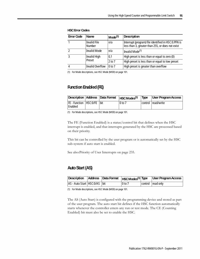
Using the High-Speed Counter and Programmable Limit Switch 91
Function Enabled (FE)
The FE (Function Enabled) is a status/control bit that defines when the HSC interrupt is enabled, and that interrupts generated by the HSC are processed based on their priority.
This bit can be controlled by the user program or is automatically set by the HSC sub-system if auto start is enabled.
See also:Priority of User Interrupts on page 235.
Auto Start (AS)
The AS (Auto Start) is configured with the programming device and stored as part of the user program. The auto start bit defines if the HSC function automatically starts whenever the controller enters any run or test mode. The CE (Counting Enabled) bit must also be set to enable the HSC.
HSC Error Codes
Error Code Name Mode(1) Description
1 Invalid File Number
n/a Interrupt (program) file identified in HSC:0.PFN is less than 3, greater than 255, or does not exist
2 Invalid Mode n/a Invalid Mode(1)
3 Invalid High Preset
0,1 High preset is less than or equal to zero (0)
2 to 7 High preset is less than or equal to low preset
4 Invalid Overflow 0 to 7 High preset is greater than overflow
(1) For Mode descriptions, see HSC Mode (MOD) on page 101.
Description Address Data Format HSC Modes(1)
(1) For Mode descriptions, see HSC Mode (MOD) on page 101.
Type User Program Access
FE - Function Enabled
HSC:0/FE bit 0 to 7 control read/write
Description Address Data Format HSC Modes(1)
(1) For Mode descriptions, see HSC Mode (MOD) on page 101.
Type User Program Access
AS - Auto Start HSC:0/AS bit 0 to 7 control read only
Publication 1762-RM001G-EN-P - September 2011

92 Using the High-Speed Counter and Programmable Limit Switch
Error Detected (ED)
The ED (Error Detected) flag is a status bit that can be used in the control program to detect if an error is present in the HSC sub-system. The most common type of error that this bit represents is a configuration error. When this bit is set (1), you should look at the specific error code in parameter HSC:0.ER.
This bit is maintained by the controller and is set and cleared automatically.
Counting Enabled (CE)
The CE (Counting Enabled) control bit is used to enable or disable the High-Speed Counter. When set (1), counting is enabled, when clear (0, default) counting is disabled. If this bit is disabled while the counter is running, the accumulated value is held; if the bit is then set, counting resumes.
This bit can be controlled by the user program and retains its value through a power cycle. This bit must be set for the high-speed counter to operate.
Set Parameters (SP)
The SP (Set Parameters) control bit is used to load new variables to the HSC sub-system. When an OTE instruction with the address of HSC:0/SP is solved true (off-to-on rung transition), all configuration variables currently stored in the HSC function are checked and loaded into the HSC sub-system. The HSC sub-system then operates based on those newly loaded settings.
Description Address Data Format HSC Modes(1)
(1) For Mode descriptions, see HSC Mode (MOD) on page 101.
Type User Program Access
ED - Error Detected
HSC:0/ED bit 0 to 7 status read only
Description Address Data Format HSC Modes(1)
(1) For Mode descriptions, see HSC Mode (MOD) on page 101.
Type User Program Access
CE - Counting Enabled
HSC:0/CE bit 0 to 7 control read/write
Description Address Data Format HSC Modes(1)
(1) For Mode descriptions, see HSC Mode (MOD) on page 101.
Type User Program Access
SP - Set Parameters
HSC:0/SP bit 0 to 7 control read/write
Publication 1762-RM001G-EN-P - September 2011

Using the High-Speed Counter and Programmable Limit Switch 93
This bit is controlled by the user program and retains its value through a power cycle. It is up to the user program to set and clear this bit. SP can be toggled while the HSC is running and no counts are lost.
User Interrupt Enable (UIE)
The UIE (User Interrupt Enable) bit is used to enable or disable HSC subroutine processing. This bit must be set (1) if the user wants the controller to process the HSC subroutine when any of the following conditions exist:
• Low preset reached• High preset reached• Overflow condition - count up through the overflow value• Underflow condition - count down through the underflow value
If this bit is cleared (0), the HSC sub-system does not automatically scan the HSC subroutine. This bit can be controlled from the user program (using the OTE, UIE, or UID instructions).
User Interrupt Executing (UIX)
The UIX (User Interrupt Executing) bit is set (1) whenever the HSC sub-system begins processing the HSC subroutine due to any of the following conditions:
• Low preset reached• High preset reached• Overflow condition - count up through the overflow value
Description Address Data Format
HSC Modes(1)
(1) For Mode descriptions, see HSC Mode (MOD) on page 101.
Type User Program Access
UIE - User Interrupt Enable HSC:0/UIE bit 0 to 7 control read/write
ATTENTION: If you enable interrupts during the program scan via an OTL, OTE, or UIE, this instruction must be the last instruction executed on the rung (last instruction on last branch). It is recommended this be the only output instruction on the rung.
Description Address Data Format
HSC Modes(1)
(1) For Mode descriptions, see HSC Mode (MOD) on page 101.
Type User Program Access
UIX - User Interrupt Executing HSC:0/UIX bit 0 to 7 status read only
Publication 1762-RM001G-EN-P - September 2011

94 Using the High-Speed Counter and Programmable Limit Switch
• Underflow condition - count down through the underflow value
The HSC UIX bit can be used in the control program as conditional logic to detect if an HSC interrupt is executing.
The HSC sub-system will clear (0) the UIX bit when the controller completes its processing of the HSC subroutine.
User Interrupt Pending (UIP)
The UIP (User Interrupt Pending) is a status flag that represents an interrupt is pending. This status bit can be monitored or used for logic purposes in the control program if you need to determine when a subroutine cannot be executed immediately.
This bit is maintained by the controller and is set and cleared automatically.
User Interrupt Lost (UIL)
The UIL (User Interrupt Lost) is a status flag that represents an interrupt has been lost. The controller can process 1 active and maintain up to 2 pending user interrupt conditions.
This bit is set by the controller. It is up to the control program to utilize, track if necessary, and clear the lost condition.
Description Address Data Format HSC Modes(1)
(1) For Mode descriptions, see HSC Mode (MOD) on page 101.
Type User Program Access
UIP - User Interrupt Pending
HSC:0/UIP bit 0 to 7 status read only
Description Address Data Format HSC Modes(1)
(1) For Mode descriptions, see HSC Mode (MOD) on page 101.
Type User Program Access
UIL - User Interrupt Lost
HSC:0/UIL bit 0 to 7 status read/write
Publication 1762-RM001G-EN-P - September 2011

Using the High-Speed Counter and Programmable Limit Switch 95
Low Preset Mask (LPM)
The LPM (Low Preset Mask) control bit is used to enable (allow) or disable (not allow) a low preset interrupt from occurring. If this bit is clear (0), and a Low Preset Reached condition is detected by the HSC, the HSC user interrupt is not executed.
This bit is controlled by the user program and retains its value through a power cycle. It is up to the user program to set and clear this bit.
Low Preset Interrupt (LPI)
The LPI (Low Preset Interrupt) status bit is set (1) when the HSC accumulator reaches the low preset value and the HSC interrupt has been triggered. This bit can be used in the control program to identify that the low preset condition caused the HSC interrupt. If the control program needs to perform any specific control action based on the low preset, this bit would be used as conditional logic.
This bit can be cleared (0) by the control program and is also be cleared by the HSC sub-system whenever these conditions are detected:
• High Preset Interrupt executes• Underflow Interrupt executes• Overflow Interrupt executes• Controller enters an executing mode
Description Address Data Format HSC Modes(1)
(1) For Mode descriptions, see HSC Mode (MOD) on page 101.
Type User Program Access
LPM - Low Preset Mask
HSC:0/LPM bit 2 to 7 control read/write
Description Address Data Format HSC Modes(1)
(1) For Mode descriptions, see HSC Mode (MOD) on page 101.
Type User Program Access
LPI - Low Preset Interrupt
HSC:0/LPI bit 2 to 7 status read/write
Publication 1762-RM001G-EN-P - September 2011

96 Using the High-Speed Counter and Programmable Limit Switch
Low Preset Reached (LPR)
The LPR (Low Preset Reached) status flag is set (1) by the HSC sub-system whenever the accumulated value (HSC:0.ACC) is less than or equal to the low preset variable (HSC:0.LOP).
This bit is updated continuously by the HSC sub-system whenever the controller is in an executing mode.
High Preset Mask (HPM)
The HPM (High Preset Mask) control bit is used to enable (allow) or disable (not allow) a high preset interrupt from occurring. If this bit is clear (0), and a High Preset Reached condition is detected by the HSC, the HSC user interrupt is not executed.
This bit is controlled by the user program and retains its value through a power cycle. It is up to the user program to set and clear this bit.
High Preset Interrupt (HPI)
The HPI (High Preset Interrupt) status bit is set (1) when the HSC accumulator reaches the high preset value and the HSC interrupt is triggered. This bit can be used in the control program to identify that the high preset condition caused the HSC interrupt. If the control program needs to perform any specific control action based on the high preset, this bit is used as conditional logic.
Description Address Data Format HSC Modes(1)
(1) For Mode descriptions, see HSC Mode (MOD) on page 101.
Type User Program Access
LPR - Low Preset Reached
HSC:0/LPR bit 2 to 7 status read only
Description Address Data Format HSC Modes(1)
(1) For Mode descriptions, see HSC Mode (MOD) on page 101.
Type User Program Access
HPM - High Preset Mask
HSC:0/HPM bit 0 to 7 control read/write
Description Address Data Format HSC Modes(1)
(1) For Mode descriptions, see HSC Mode (MOD) on page 101.
Type User Program Access
HPI - High Preset Interrupt
HSC:0/HPI bit 0 to 7 status read/write
Publication 1762-RM001G-EN-P - September 2011

Using the High-Speed Counter and Programmable Limit Switch 97
This bit can be cleared (0) by the control program and is also cleared by the HSC sub-system whenever these conditions are detected:
• Low Preset Interrupt executes• Underflow Interrupt executes• Overflow Interrupt executes• Controller enters an executing mode
High Preset Reached (HPR)
The HPR (High Preset Reached) status flag is set (1) by the HSC sub-system whenever the accumulated value (HSC:0.ACC) is greater than or equal to the high preset variable (HSC:0.HIP).
This bit is updated continuously by the HSC sub-system whenever the controller is in an executing mode.
Underflow (UF)
The UF (Underflow) status flag is set (1) by the HSC sub-system whenever the accumulated value (HSC:0.ACC) has counted through the underflow variable (HSC:0.UNF).
This bit is transitional and is set by the HSC sub-system. It is up to the control program to utilize, track if necessary, and clear (0) the underflow condition.
Underflow conditions do not generate a controller fault.
Description Address Data Format HSC Modes(1)
(1) For Mode descriptions, see HSC Mode (MOD) on page 101.
Type User Program Access
HPR - High Preset Reached
HSC:0/HPR bit 2 to 7 status read only
Description Address Data Format HSC Modes(1)
(1) For Mode descriptions, see HSC Mode (MOD) on page 101.
Type User Program Access
UF - Underflow HSC:0/UF bit 0 to 7 status read/write
Publication 1762-RM001G-EN-P - September 2011
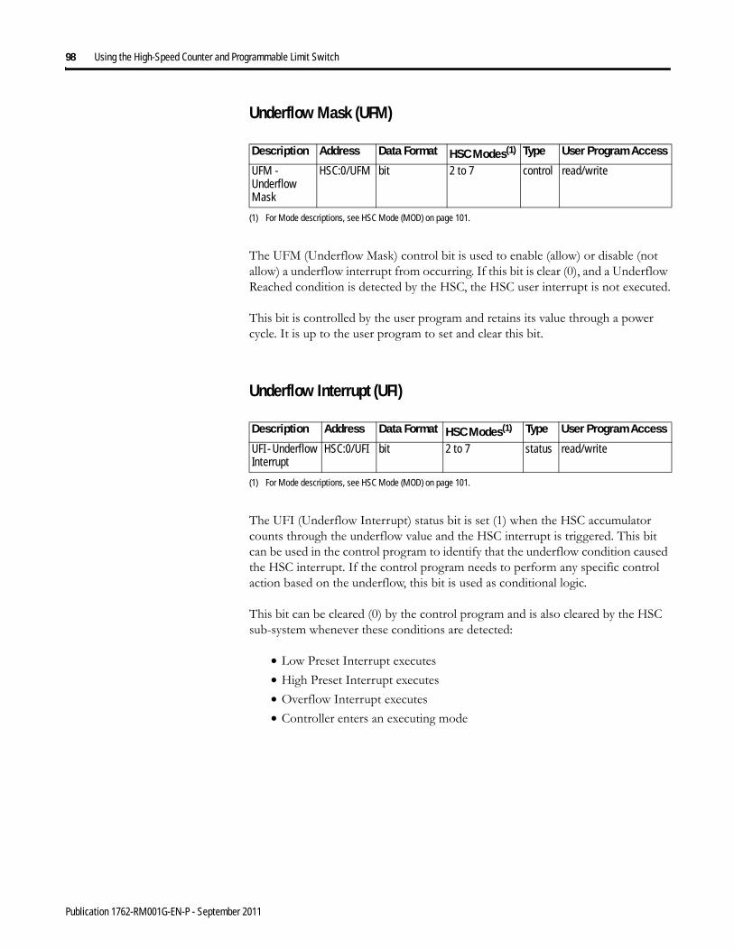
98 Using the High-Speed Counter and Programmable Limit Switch
Underflow Mask (UFM)
The UFM (Underflow Mask) control bit is used to enable (allow) or disable (not allow) a underflow interrupt from occurring. If this bit is clear (0), and a Underflow Reached condition is detected by the HSC, the HSC user interrupt is not executed.
This bit is controlled by the user program and retains its value through a power cycle. It is up to the user program to set and clear this bit.
Underflow Interrupt (UFI)
The UFI (Underflow Interrupt) status bit is set (1) when the HSC accumulator counts through the underflow value and the HSC interrupt is triggered. This bit can be used in the control program to identify that the underflow condition caused the HSC interrupt. If the control program needs to perform any specific control action based on the underflow, this bit is used as conditional logic.
This bit can be cleared (0) by the control program and is also cleared by the HSC sub-system whenever these conditions are detected:
• Low Preset Interrupt executes• High Preset Interrupt executes• Overflow Interrupt executes• Controller enters an executing mode
Description Address Data Format HSC Modes(1)
(1) For Mode descriptions, see HSC Mode (MOD) on page 101.
Type User Program Access
UFM - Underflow Mask
HSC:0/UFM bit 2 to 7 control read/write
Description Address Data Format HSC Modes(1)
(1) For Mode descriptions, see HSC Mode (MOD) on page 101.
Type User Program Access
UFI - Underflow Interrupt
HSC:0/UFI bit 2 to 7 status read/write
Publication 1762-RM001G-EN-P - September 2011
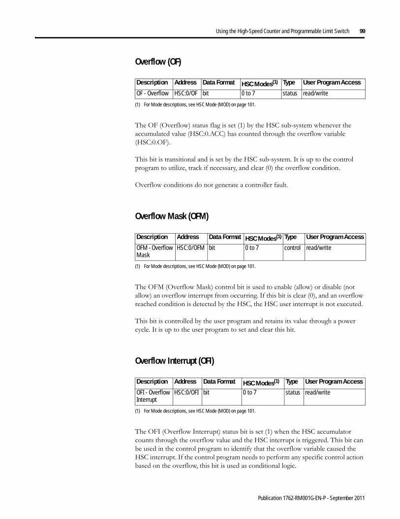
Using the High-Speed Counter and Programmable Limit Switch 99
Overflow (OF)
The OF (Overflow) status flag is set (1) by the HSC sub-system whenever the accumulated value (HSC:0.ACC) has counted through the overflow variable (HSC:0.OF).
This bit is transitional and is set by the HSC sub-system. It is up to the control program to utilize, track if necessary, and clear (0) the overflow condition.
Overflow conditions do not generate a controller fault.
Overflow Mask (OFM)
The OFM (Overflow Mask) control bit is used to enable (allow) or disable (not allow) an overflow interrupt from occurring. If this bit is clear (0), and an overflow reached condition is detected by the HSC, the HSC user interrupt is not executed.
This bit is controlled by the user program and retains its value through a power cycle. It is up to the user program to set and clear this bit.
Overflow Interrupt (OFI)
The OFI (Overflow Interrupt) status bit is set (1) when the HSC accumulator counts through the overflow value and the HSC interrupt is triggered. This bit can be used in the control program to identify that the overflow variable caused the HSC interrupt. If the control program needs to perform any specific control action based on the overflow, this bit is used as conditional logic.
Description Address Data Format HSC Modes(1)
(1) For Mode descriptions, see HSC Mode (MOD) on page 101.
Type User Program Access
OF - Overflow HSC:0/OF bit 0 to 7 status read/write
Description Address Data Format HSC Modes(1)
(1) For Mode descriptions, see HSC Mode (MOD) on page 101.
Type User Program Access
OFM - Overflow Mask
HSC:0/OFM bit 0 to 7 control read/write
Description Address Data Format HSC Modes(1)
(1) For Mode descriptions, see HSC Mode (MOD) on page 101.
Type User Program Access
OFI - Overflow Interrupt
HSC:0/OFI bit 0 to 7 status read/write
Publication 1762-RM001G-EN-P - September 2011

100 Using the High-Speed Counter and Programmable Limit Switch
This bit can be cleared (0) by the control program and is also cleared by the HSC sub-system whenever these conditions are detected:
• Low Preset Interrupt executes• High Preset Interrupt executes• Underflow Interrupt executes• Controller enters an executing mode
Count Direction (DIR)
The DIR (Count Direction) status flag is controlled by the HSC sub-system. When the HSC accumulator counts up, the direction flag is set (1). Whenever the HSC accumulator counts down, the direction flag is cleared (0).
If the accumulated value stops, the direction bit retains its value. The only time the direction flag changes is when the accumulated count reverses.
This bit is updated continuously by the HSC sub-system whenever the controller is in a run mode.
Mode Done (MD)
The MD (Mode Done) status flag is set (1) by the HSC sub-system when the HSC is configured for Mode 0 or Mode 1 behavior, and the accumulator counts up to the High Preset.
Description Address Data Format HSC Modes(1)
(1) For Mode descriptions, see HSC Mode (MOD) on page 101.
Type User Program Access
DIR - Count Direction
HSC:0/DIR bit 0 to 7 status read only
Description Address Data Format HSC Modes(1)
(1) For Mode descriptions, see HSC Mode (MOD) on page 101.
Type User Program Access
MD - Mode Done
HSC:0/MD bit 0 or 1 status read/write
Publication 1762-RM001G-EN-P - September 2011

Using the High-Speed Counter and Programmable Limit Switch 101
Count Down (CD)
The CD (Count Down) bit is used with the bidirectional counters (modes 2 to 7). If the CE bit is set, the CD bit is set (1). If the CE bit is clear, the CD bit is cleared (0).
Count Up (CU)
The CU (Count Up) bit is used with all of the HSCs (modes 0 to 7). If the CE bit is set, the CU bit is set (1). If the CE bit is clear, the CU bit is cleared (0).
HSC Mode (MOD)
The MOD (Mode) variable sets the High-Speed Counter to one of 8 types of operation. This integer value is configured through the programming device and is accessible in the control program as a read-only variable.
Description Address Data Format HSC Modes(1)
(1) For Mode descriptions, see HSC Mode (MOD) on page 101.
Type User Program Access
CD - Count Down HSC:0/CD bit 2 to 7 status read only
Description Address Data Format HSC Modes(1)
(1) For Mode descriptions, see HSC Mode (MOD) on page 101.
Type User Program Access
CU - Count Up HSC:0/CU bit 0 to 7 status read only
Description Address Data Format Type User Program AccessMOD - HSC Mode HSC:0.MOD word (INT) control read only
HSC Operating Modes
Mode Number
Type
0 Up Counter - The accumulator is immediately cleared (0) when it reaches the high preset. A low preset cannot be defined in this mode.
1 Up Counter with external reset and hold - The accumulator is immediately cleared (0) when it reaches the high preset. A low preset cannot be defined in this mode.
2 Counter with external direction
3 Counter with external direction, reset, and hold
4 Two input counter (up and down)
5 Two input counter (up and down) with external reset and hold
6 Quadrature counter (phased inputs A and B)
7 Quadrature counter (phased inputs A and B) with external reset and hold
Publication 1762-RM001G-EN-P - September 2011
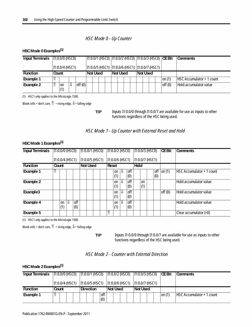
102 Using the High-Speed Counter and Programmable Limit Switch
HSC Mode 0 - Up Counter
HSC Mode 1 - Up Counter with External Reset and Hold
HSC Mode 2 - Counter with External Direction
HSC Mode 0 Examples(1)
Input Terminals I1:0.0/0 (HSC0)
I1:0.0/4 (HSC1)
I1:0.0/1 (HSC0)
I1:0.0/5 (HSC1)
I1:0.0/2 (HSC0)
I1:0.0/6 (HSC1)
I1:0.0/3 (HSC0)
I1:0.0/7 (HSC1)
CE Bit Comments
Function Count Not Used Not Used Not UsedExample 1 ⇑ on (1) HSC Accumulator + 1 countExample 2 ⇑ on
(1)⇓ off (0) off (0) Hold accumulator value
(1) HSC1 only applies to the MicroLogix 1500.
Blank cells = don’t care, ⇑ = rising edge, ⇓ = falling edge
TIP Inputs I1:0.0/0 through I1:0.0/7 are available for use as inputs to other functions regardless of the HSC being used.
HSC Mode 1 Examples(1)
Input Terminals I1:0.0/0 (HSC0)
I1:0.0/4 (HSC1)
I1:0.0/1 (HSC0)
I1:0.0/5 (HSC1)
I1:0.0/2 (HSC0)
I1:0.0/6 (HSC1)
I1:0.0/3 (HSC0)
I1:0.0/7 (HSC1)
CE Bit Comments
Function Count Not Used Reset HoldExample 1 ⇑ on
(1)⇓ off
(0)off (0)
on (1) HSC Accumulator + 1 count
Example 2 on (1)
⇓ off (0)
on (1)
Hold accumulator value
Example3 on (1)
⇓ off (0)
off (0) Hold accumulator value
Example 4 on (1)
⇓ off (0)
on (1)
⇓ off (0)
Hold accumulator value
Example 5 ⇑ Clear accumulator (=0)
(1) HSC1 only applies to the MicroLogix 1500.
Blank cells = don’t care, ⇑ = rising edge, ⇓ = falling edge
TIP Inputs I1:0.0/0 through I1:0.0/7 are available for use as inputs to other functions regardless of the HSC being used.
HSC Mode 2 Examples(1)
Input Terminals I1:0.0/0 (HSC0)
I1:0.0/4 (HSC1)
I1:0.0/1 (HSC0)
I1:0.0/5 (HSC1)
I1:0.0/2 (HSC0)
I1:0.0/6 (HSC1)
I1:0.0/3 (HSC0)
I1:0.0/7 (HSC1)
CE Bit Comments
Function Count Direction Not Used Not UsedExample 1 ⇑ off
(0)on (1) HSC Accumulator + 1 count
Publication 1762-RM001G-EN-P - September 2011

Using the High-Speed Counter and Programmable Limit Switch 103
HSC Mode 3 - Counter with External Direction, Reset, and Hold
HSC Mode 4 - Two Input Counter (up and down)
Example 2 ⇑ on (1)
on (1) HSC Accumulator - 1 count
Example3 off (0) Hold accumulator value
(1) HSC1 only applies to the MicroLogix 1500.
Blank cells = don’t care, ⇑ = rising edge, ⇓ = falling edge
HSC Mode 2 Examples(1)
Input Terminals I1:0.0/0 (HSC0)
I1:0.0/4 (HSC1)
I1:0.0/1 (HSC0)
I1:0.0/5 (HSC1)
I1:0.0/2 (HSC0)
I1:0.0/6 (HSC1)
I1:0.0/3 (HSC0)
I1:0.0/7 (HSC1)
CE Bit Comments
TIP Inputs I1:0.0/0 through I1:0.0/7 are available for use as inputs to other functions regardless of the HSC being used.
HSC Mode 3 Examples(1)
Input Terminals I1:0.0/0 (HSC0)
I1:0.0/4 (HSC1)
I1:0.0/1 (HSC0)
I1:0.0/5 (HSC1)
I1:0.0/2 (HSC0)
I1:0.0/6 (HSC1)
I1:0.0/3 (HSC0)
I1:0.0/7 (HSC1)
CE Bit Comments
Function Count Direction Reset HoldExample 1 ⇑ off
(0)on (1)
⇓ off (0)
off (0)
on (1) HSC Accumulator + 1 count
Example 2 ⇑ on (1)
on (1)
⇓ off (0)
off (0)
on (1) HSC Accumulator - 1 count
Example3 on (1)
⇓ off (0)
on (1)
Hold accumulator value
Example 4 on (1)
⇓ off (0)
off (0) Hold accumulator value
Example 5 on (1)
⇓ off (0)
on (1)
⇓ off (0)
Hold accumulator value
Example 6 ⇑ Clear accumulator (=0)
(1) HSC1 only applies to the MicroLogix 1500.
Blank cells = don’t care, ⇑ = rising edge, ⇓ = falling edge
TIP Inputs I1:0.0/0 through I1:0.0/7 are available for use as inputs to other functions regardless of the HSC being used.
HSC Mode 4 Examples(1)
Input Terminals I1:0.0/0 (HSC0)
I1:0.0/4 (HSC1)
I1:0.0/1 (HSC0)
I1:0.0/5 (HSC1)
I1:0.0/2 (HSC0)
I1:0.0/6 (HSC1)
I1:0.0/3 (HSC0)
I1:0.0/7 (HSC1)
CE Bit Comments
Function Count Up Count Down Not Used Not UsedExample 1 ⇑ on
(1)⇓ off
(0)on (1) HSC Accumulator + 1 count
Publication 1762-RM001G-EN-P - September 2011

104 Using the High-Speed Counter and Programmable Limit Switch
HSC Mode 5 - Two Input Counter (up and down) with External Reset and Hold
Using the Quadrature Encoder
The Quadrature Encoder is used for determining direction of rotation and position for rotating, such as a lathe. The Bidirectional Counter counts the rotation of the Quadrature Encoder.
The figure below shows a quadrature encoder connected to inputs 0, 1, and 2. The count direction is determined by the phase angle between A and B. If A leads B, the counter increments. If B leads A, the counter decrements.
Example 2 on (1)
⇓ off (0)
⇑ on (1) HSC Accumulator - 1 count
Example3 off (0) Hold accumulator value
(1) HSC1 only applies to the MicroLogix 1500.
Blank cells = don’t care, ⇑ = rising edge, ⇓ = falling edge
HSC Mode 4 Examples(1)
Input Terminals I1:0.0/0 (HSC0)
I1:0.0/4 (HSC1)
I1:0.0/1 (HSC0)
I1:0.0/5 (HSC1)
I1:0.0/2 (HSC0)
I1:0.0/6 (HSC1)
I1:0.0/3 (HSC0)
I1:0.0/7 (HSC1)
CE Bit Comments
TIP Inputs I1:0.0/0 through I1:0.0/7 are available for use as inputs to other functions regardless of the HSC being used.
HSC Mode 5 Examples(1)
Input Terminals I1:0.0/0 (HSC0)
I1:0.0/4 (HSC1)
I1:0.0/1 (HSC0)
I1:0.0/5 (HSC1)
I1:0.0/2 (HSC0)
I1:0.0/6 (HSC1)
I1:0.0/3 (HSC0)
I1:0.0/7 (HSC1)
CE Bit Comments
Function Count Direction Reset HoldExample 1 ⇑ on
(1)⇓ off
(0)on (1)
⇓ off (0)
off (0)
on (1) HSC Accumulator + 1 count
Example 2 on (1)
⇓ off (0)
⇑ on (1)
⇓ off (0)
off (0)
on (1) HSC Accumulator - 1 count
Example3 on (1)
⇓ off (0)
on (1)
Hold accumulator value
Example 4 on (1)
⇓ off (0)
off (0) Hold accumulator value
Example 5 on (1)
⇓ off (0)
on (1)
⇓ off (0)
Hold accumulator value
Example 6 ⇑ Clear accumulator (=0)
(1) HSC1 only applies to the MicroLogix 1500.
Blank cells = don’t care, ⇑ = rising edge, ⇓ = falling edge
TIP Inputs I1:0.0/0 through I1:0.0/7 are available for use as inputs to other functions regardless of the HSC being used.
Publication 1762-RM001G-EN-P - September 2011
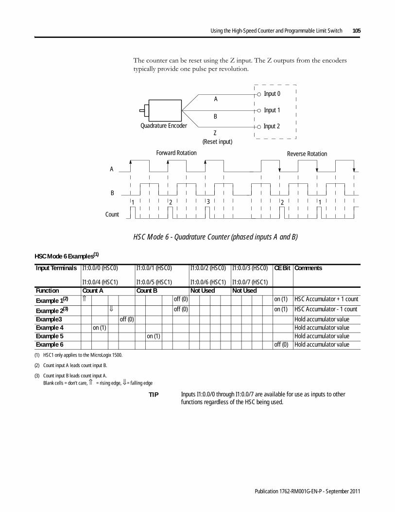
Using the High-Speed Counter and Programmable Limit Switch 105
The counter can be reset using the Z input. The Z outputs from the encoders typically provide one pulse per revolution.
HSC Mode 6 - Quadrature Counter (phased inputs A and B)
Quadrature Encoder
Input 0
Input 1
Input 2
A
B
Z(Reset input)
Reverse RotationForward Rotation
B
A
1 2 3 2 1
Count
HSC Mode 6 Examples(1)
Input Terminals I1:0.0/0 (HSC0)
I1:0.0/4 (HSC1)
I1:0.0/1 (HSC0)
I1:0.0/5 (HSC1)
I1:0.0/2 (HSC0)
I1:0.0/6 (HSC1)
I1:0.0/3 (HSC0)
I1:0.0/7 (HSC1)
CE Bit Comments
Function Count A Count B Not Used Not Used
Example 1(2) ⇑ off (0) on (1) HSC Accumulator + 1 count
Example 2(3) ⇓ off (0) on (1) HSC Accumulator - 1 count
Example3 off (0) Hold accumulator valueExample 4 on (1) Hold accumulator valueExample 5 on (1) Hold accumulator valueExample 6 off (0) Hold accumulator value
(1) HSC1 only applies to the MicroLogix 1500.
(2) Count input A leads count input B.
(3) Count input B leads count input A.Blank cells = don’t care, ⇑ = rising edge, ⇓ = falling edge
TIP Inputs I1:0.0/0 through I1:0.0/7 are available for use as inputs to other functions regardless of the HSC being used.
Publication 1762-RM001G-EN-P - September 2011
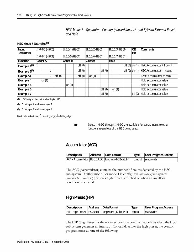
106 Using the High-Speed Counter and Programmable Limit Switch
HSC Mode 7 - Quadrature Counter (phased inputs A and B) With External Reset and Hold
Blank cells = don’t care, ⇑ = rising edge, ⇓ = falling edge
Accumulator (ACC)
The ACC (Accumulator) contains the number of counts detected by the HSC sub-system. If either mode 0 or mode 1 is configured, the value of the software accumulator is cleared (0) when a high preset is reached or when an overflow condition is detected.
High Preset (HIP)
The HIP (High Preset) is the upper setpoint (in counts) that defines when the HSC sub-system generates an interrupt. To load data into the high preset, the control program must do one of the following:
HSC Mode 7 Examples(1)
Input Terminals
I1:0.0/0 (HSC0)
I1:0.0/4 (HSC1)
I1:0.0/1 (HSC0)
I1:0.0/5 (HSC1)
I1:0.0/2 (HSC0)
I1:0.0/6 (HSC1)
I1:0.0/3 (HSC0)
I1:0.0/7 (HSC1)
CE Bit
Comments
Function Count A Count B Z reset Hold
Example 1(2) ⇑ off (0) off (0) on (1) HSC Accumulator + 1 count
Example 2(3) ⇓ off (0) off (0) off (0) on (1) HSC Accumulator - 1 count
Example3 ⇓ off (0) off (0) on (1) Reset accumulator to zeroExample 4 on (1) Hold accumulator valueExample 5 on (1) Hold accumulator valueExample 6 off (0) on (1) Hold accumulator valueExample 7 off (0) off (0) Hold accumulator value
(1) HSC1 only applies to the MicroLogix 1500.
(2) Count input A leads count input B.
(3) Count input B leads count input A.
TIP Inputs I1:0.0/0 through I1:0.0/7 are available for use as inputs to other functions regardless of the HSC being used.
Description Address Data Format Type User Program AccessACC - Accumulator HSC:0.ACC long word (32-bit INT) control read/write
Description Address Data Format Type User Program AccessHIP - High Preset HSC:0.HIP long word (32-bit INT) control read/write
Publication 1762-RM001G-EN-P - September 2011
Using the High-Speed Counter and Programmable Limit Switch 107
• Toggle (low to high) the Set Parameters (HSC:0/SP) control bit. When the SP bit is toggled high, the data currently stored in the HSC function file is transferred/loaded into the HSC sub-system.
• Load new HSC parameters using the HSL instruction. See HSL - High-Speed Counter Load on page 110.
The data loaded into the high preset must be less than or equal to the data resident in the overflow (HSC:0.OVF) parameter or an HSC error is generated.
Low Preset (LOP)
The LOP (Low Preset) is the lower setpoint (in counts) that defines when the HSC sub-system generates an interrupt. To load data into the low preset, the control program must do one of the following:
• Toggle (low to high) the Set Parameters (HSC:0/SP) control bit. When the SP bit is toggled high, the data currently stored in the HSC function file is transferred/loaded into the HSC sub-system.
• Load new HSC parameters using the HSL instruction. See HSL - High-Speed Counter Load on page 110.
The data loaded into the low preset must greater than or equal to the data resident in the underflow (HSC:0.UNF) parameter, or an HSC error is generated. (If the underflow and low preset values are negative numbers, the low preset must be a number with a smaller absolute value.)
Overflow (OVF)
The OVF (Overflow) defines the upper count limit for the counter. If the counter’s accumulated value increments past the value specified in this variable, an overflow interrupt is generated. When the overflow interrupt is generated, the HSC sub-system rolls the accumulator over to the underflow value and the counter continues counting from the underflow value (counts are not lost in this transition). The user can specify any value for the overflow position, provided it is greater than the underflow value and falls between -2,147,483,648 and 2,147,483,647.
Description Address Data Format Type User Program AccessLOP - Low Preset HSC:0.LOP long word (32-bit INT) control read/write
Description Address Data Format Type User Program AccessOVF - Overflow HSC:0.OVF long word (32-bit INT) control read/write
Publication 1762-RM001G-EN-P - September 2011

108 Using the High-Speed Counter and Programmable Limit Switch
To load data into the overflow variable, the control program must toggle (low to high) the Set Parameters (HSC:0.0/SP) control bit. When the SP bit is toggled high, the data currently stored in the HSC function file is transferred/loaded into the HSC sub-system.
Underflow (UNF)
The UNF (Underflow) defines the lower count limit for the counter. If the counter’s accumulated value decrements past the value specified in this variable, an underflow interrupt is generated. When the underflow interrupt is generated, the HSC sub-system resets the accumulated value to the overflow value and the counter then begins counting from the overflow value (counts are not lost in this transition). The user can specify any value for the underflow position, provided it is less than the overflow value and falls between -2,147,483,648 and 2,147,483,647.
To load data into the underflow variable, the control program must toggle (low to high) the Set Parameters (HSC:0.0/SP) control bit. When the SP bit is toggled high, the data currently stored in the HSC function file is transferred/loaded into the HSC sub-system.
TIP Data loaded into the overflow variable must be greater than the data resident in the high preset (HSC:0.HIP) or an HSC error is generated.
Description Address Data Format Type User Program AccessUNF - Underflow HSC:0.UNF long word (32-bit INT) control read/write
Publication 1762-RM001G-EN-P - September 2011

Using the High-Speed Counter and Programmable Limit Switch 109
Output Mask Bits (OMB)
The OMB (Output Mask Bits) define which outputs on the controller can be directly controlled by the high-speed counter. The HSC sub-system has the ability to directly (without control program interaction) turn outputs ON or OFF based on the HSC accumulator reaching the High or Low presets. The bit pattern stored in the OMB variable defines which outputs are controlled by the HSC and which outputs are not controlled by the HSC.
The bit pattern of the OMB variable directly corresponds to the output bits on the controller. Bits that are set (1) are enabled and can be turned on or off by the HSC sub-system. Bits that are clear (0) cannot be turned on or off by the HSC sub-system. The mask bit pattern can be configured only during initial setup.
The table below illustrates this relationship:
The outputs shown in the black boxes are the outputs under the control of the HSC sub-system. The mask defines which outputs can be controlled. The high preset output or low preset output values (HPO or LPO) define if each output is either ON (1) or OFF (0). Another way to view this is that the high or low preset output is written through the output mask, with the output mask acting like a filter.
The bits in the gray boxes are unused. The first 12 bits of the mask word are used and the remaining mask bits are not functional because they do not correlate to any physical outputs on the base unit.
The mask bit pattern can be configured only during initial setup.
TIP Data loaded into the overflow variable must be greater than the data resident in the high preset (HSC:0.HIP) or an HSC error is generated.
Description Address Data Format Type User Program AccessOMB - Output Mask Bits HSC:0.OMB word (16-bit binary) control read only
Affect of HSC Output Mask on Base Unit Outputs
Output Address 16-Bit Signed Integer Data Word15 14 13 12 11 10 9 8 7 6 5 4 3 2 1 0
HSC:0.HPO (high preset output) 0 1 1 0 1 0 0 1 1 0 0 1
HSC:0.OMB (output mask) 1 0 0 0 0 1 1 1 0 0 1 1
O0:0.0 0 0 0 1 0 1
Publication 1762-RM001G-EN-P - September 2011

110 Using the High-Speed Counter and Programmable Limit Switch
High Preset Output (HPO)
The HPO (High Preset Output) defines the state (1 = ON or 0 = OFF) of the outputs on the controller when the high preset is reached. See Output Mask Bits (OMB) on page 109 for more information on how to directly turn outputs on or off based on the high preset being reached.
The high output bit pattern can be configured during initial setup, or while the controller is operating. Use the HSL instruction or the SP bit to load the new parameters while the controller is operating.
Low Preset Output (LPO)
The LPO (Low Preset Output) defines the state (1 = “on”, 0 = “off ”) of the outputs on the controller when the low preset is reached. See Output Mask Bits (OMB) on page 109 for more information on how to directly turn outputs on or off based on the low preset being reached.
The low output bit pattern can be configured during initial setup, or while the controller is operating. Use the HSL instruction or the SP bit to load the new parameters while the controller is operating.
HSL - High-Speed Counter Load
Instruction Type: output
The HSL (High-Speed Load) instruction allows the high and low presets, and high and low output source to be applied to a high-speed counter. These parameters are described below:
Description Address Data Format Type User Program AccessHPO - High Preset Output HSC:0.HPO word (16-bit binary) control read/write
Description Address Data Format Type User Program AccessLPO - Low Preset Output HSC:0.LPO word (16-bit binary) control read/write
HSLHigh Speed Counter LoadHSC Number HSC0High Preset N7:0Low Preset N7:1Output High Source N7:2Output Low Source N7:3
HSL
Controller Data Size Execution Time When Rung Is:True False
MicroLogix 1200 word 46.7 μs 0.0 μslong word 47.3 μs 0.0 μs
MicroLogix 1500 word 39.7 μs 0.0 μslong word 40.3 μs 0.0 μs
Publication 1762-RM001G-EN-P - September 2011

Using the High-Speed Counter and Programmable Limit Switch 111
• Counter Number - Specifies which high-speed counter is being used; 0 = HSC0 and 1 = HSC1 (MicroLogix 1500 only).
• High Preset - Specifies the value in the high preset register. The data ranges for the high preset are -32786 to 32767 (word) and -2,147,483,648 to 2,147,483,647 (long word).
• Low Preset - Specifies the value in the low preset register. The data ranges for the low preset are -32786 to 32767 (word) and -2,147,483,648 to 2,147,483,647 (long word).
• Output High Source - Specifies the value in the HPO - high preset output register. The data range for the output high source is from 0 to 65,535.
• Output Low Source - Specifies the value in the LPO - low preset output register. The data range for the output low source is from 0 to 65,535.
Valid Addressing Modes and File Types are shown below:
RAC - Reset Accumulated Value
Instruction Type: output
The RAC instruction resets the high-speed counter and allows a specific value to be written to the HSC accumulator. The RAC instruction uses the following parameters:
• Counter Number - Specifies which high-speed counter is being used:– Counter Number 0 = HSC0 (MicroLogix 1200 and 1500)– Counter Number 1 = HSC1 (MicroLogix 1500 only)
• Source - Specifies the location of the data to be loaded into the HSC accumulator. The data range is from -2,147,483,648 to 2,147,483,647.
HSL Instruction Valid Addressing Modes and File TypesFor definitions of the terms used in this table see Using the Instruction Descriptions on page 82.
Parameter
Data Files Function Files
CS -
Com
ms
IOS
- I/O
DLS
- D
ata
Log
Address Mode
Address Level
O I S B T, C
, R
N F ST L MG
, PD
PLS
RTC
HSC
PTO
, PW
M
STI
EII
BHI
MM
I
DAT
TPI
Imm
edia
te
Dir
ect
Indi
rect
Bit
Wor
d
Long
Wor
d
Elem
ent
Counter Number •High Preset • • • • • • • • • • •
Low Preset • • • • • • • • • • •
Output High Source • • • • • • • • • • •
Output Low Source • • • • • • • • • • •
RACReset Accumulated ValueCounter HSC0Source 0
RAC
Controller Execution Time When Rung Is:True False
MicroLogix 1200 21.2 μs 0.0 μsMicroLogix 1500 17.8 μs 0.0 μs
Publication 1762-RM001G-EN-P - September 2011
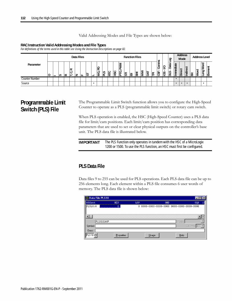
112 Using the High-Speed Counter and Programmable Limit Switch
Valid Addressing Modes and File Types are shown below:
Programmable Limit Switch (PLS) File
The Programmable Limit Switch function allows you to configure the High-Speed Counter to operate as a PLS (programmable limit switch) or rotary cam switch.
When PLS operation is enabled, the HSC (High-Speed Counter) uses a PLS data file for limit/cam positions. Each limit/cam position has corresponding data parameters that are used to set or clear physical outputs on the controller’s base unit. The PLS data file is illustrated below.
PLS Data File
Data files 9 to 255 can be used for PLS operations. Each PLS data file can be up to 256 elements long. Each element within a PLS file consumes 6 user words of memory. The PLS data file is shown below:
RAC Instruction Valid Addressing Modes and File TypesFor definitions of the terms used in this table see Using the Instruction Descriptions on page 82.
Parameter
Data Files Function Files
CSF
- Com
ms
IOS
- I/O
DLS
- Da
ta L
og
Address Mode
Address Level
O I S B T, C
, R
N F ST L MG
, PD
PLS
RTC
HSC
PTO
, PW
M
STI
EII
BHI
MM
I
DAT
TPI
Imm
edia
te
Dir
ect
Indi
rect
Bit
Wor
d
Long
Wor
d
Elem
ent
Counter Number •Source • • • • •
IMPORTANT The PLS Function only operates in tandem with the HSC of a MicroLogix 1200 or 1500. To use the PLS function, an HSC must first be configured.
Publication 1762-RM001G-EN-P - September 2011

Using the High-Speed Counter and Programmable Limit Switch 113
PLS Operation
When the PLS function is enabled, and the controller is in the run mode, the HSC will count incoming pulses. When the count reaches the first preset (High - HIP or Low - LOP) defined in the PLS file, the output source data (High - OHD or Low - OLD) will be written through the HSC mask.
At that point, the next preset (High - HIP or Low - LOP) defined in the PLS file becomes active.
When the HSC counts to that new preset, the new output data is written through the HSC mask. This process continues until the last element within the PLS file is loaded. At that point the active element within the PLS file is reset to zero. This behavior is referred to as circular operation.
If invalid data is loaded during operation, an HSC error is generated (within the HSC function file). The error will not cause a controller fault. If an invalid parameter is detected, it will be skipped and the next parameter will be loaded for execution (provided it is valid).
You can use the PLS in Up (high), Down (low), or both directions. If your application only counts in one direction, simply ignore the other parameters.
The PLS function can operate with all of the other HSC capabilities. The ability to select which HSC events generate a user interrupt are not limited.
TIP The Output High Data (OHD) is only written when the High preset (HIP) is reached. The Output Low Data (OLD) is written when the low preset is reached.
TIP Output High Data is only operational when the counter is counting up. Output Low Data is only operational when the counter is counting down.
Publication 1762-RM001G-EN-P - September 2011

114 Using the High-Speed Counter and Programmable Limit Switch
Addressing PLS Files
The addressing format for the PLS file is shown below.
PLS Example
Setting up the PLS File
1. Using RSLogix 500, create a new project, give it a name and select the appropriate controller.
Format ExplanationPLSf:e.s PLS Programmable Limit Switch file
f File number The valid file number range is from 9 to 255.
: Element delimiter
e Element number The valid element number range is from 0 to 255.
. Sub-Element delimiter
s Sub-Element number The valid sub-element number range is from 0 to 5
Examples: PLS10:2
PLS12:36.5
PLS File 10, Element 2
PLS File 12, Element 36, Sub-Element 5 (Output Low Source)
Publication 1762-RM001G-EN-P - September 2011
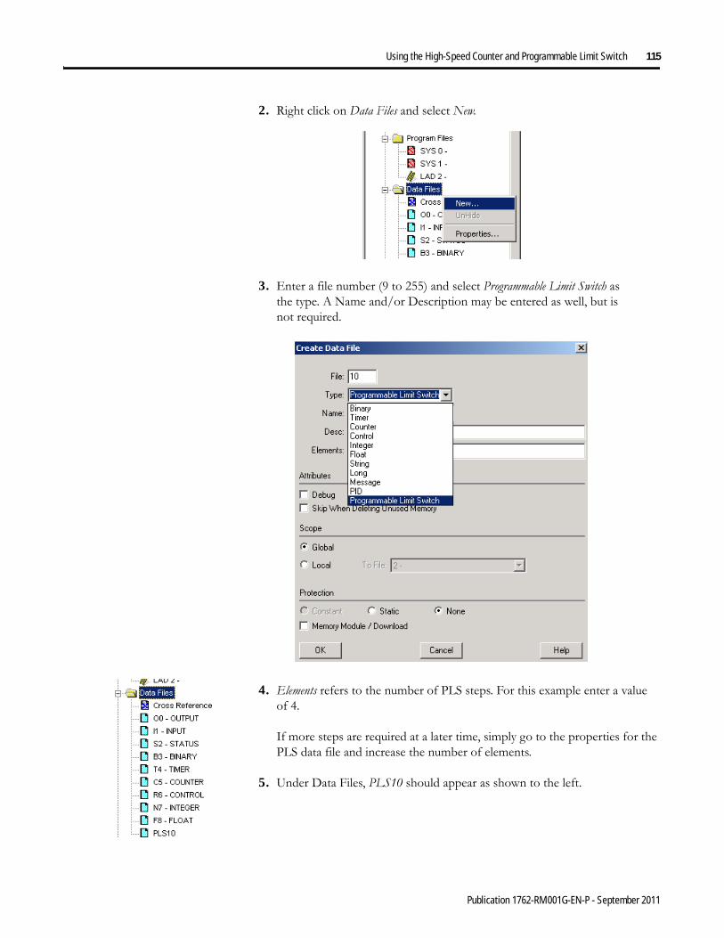
Using the High-Speed Counter and Programmable Limit Switch 115
2. Right click on Data Files and select New.
3. Enter a file number (9 to 255) and select Programmable Limit Switch as the type. A Name and/or Description may be entered as well, but is not required.
4. Elements refers to the number of PLS steps. For this example enter a value of 4.
If more steps are required at a later time, simply go to the properties for the PLS data file and increase the number of elements.
5. Under Data Files, PLS10 should appear as shown to the left.
Publication 1762-RM001G-EN-P - September 2011
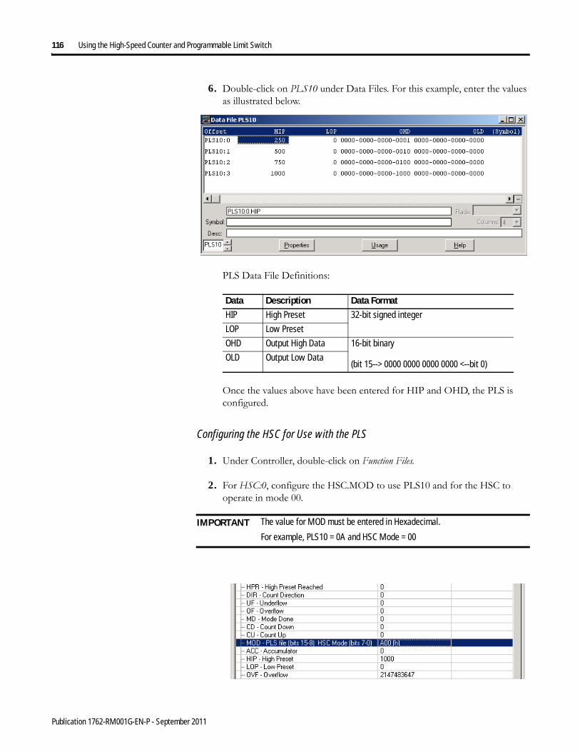
116 Using the High-Speed Counter and Programmable Limit Switch
6. Double-click on PLS10 under Data Files. For this example, enter the values as illustrated below.
PLS Data File Definitions:
Once the values above have been entered for HIP and OHD, the PLS is configured.
Configuring the HSC for Use with the PLS
1. Under Controller, double-click on Function Files.
2. For HSC:0, configure the HSC.MOD to use PLS10 and for the HSC to operate in mode 00.
Data Description Data FormatHIP High Preset 32-bit signed integer
LOP Low Preset
OHD Output High Data 16-bit binary
(bit 15--> 0000 0000 0000 0000 <--bit 0)OLD Output Low Data
IMPORTANT The value for MOD must be entered in Hexadecimal.
For example, PLS10 = 0A and HSC Mode = 00
Publication 1762-RM001G-EN-P - September 2011
Using the High-Speed Counter and Programmable Limit Switch 117
PLS Operation for This Example
When the ladder logic first runs, HSC.ACC equals 0, therefore PLS10:0.OLD's data is sent through the HSC.OMB mask and sets all the outputs off.
When HSC.ACC equals 250, the PLS10:0.OHD is sent through the HSC.OMB mask and energizes the outputs.
This will repeat as the HSC.ACC reaches 500, 750, and 1000. Once completed, the cycle resets and repeats.
Publication 1762-RM001G-EN-P - September 2011

118 Using the High-Speed Counter and Programmable Limit Switch
Publication 1762-RM001G-EN-P - September 2011

Chapter 6
Using High-Speed Outputs
The high-speed output instructions allow you to control and monitor the PTO and PWM functions which control the physical high-speed outputs.
PTO - Pulse Train Output
Instruction Type: output
Pulse Train Output Function
The MicroLogix 1200 1762-L24BXB and 1762-L40BXB controllers each support one high-speed output. A MicroLogix 1500 controller utilizing a 1764-28BXB Base Unit supports two high-speed outputs. These outputs can be used as standard outputs (not high-speed) or individually configured for PTO or PWM operation. The PTO functionality allows a simple motion profile or pulse profile to be generated directly from the controller. The pulse profile has three primary components:
• Total number of pulses to be generated• Accelerate/decelerate intervals• Run interval
Instruction Used To: Page
PTO - Pulse Train Output Generate stepper pulses 119
PWM - Pulse Width Modulation Generate PWM output 137
PTOPulse Train OutputPTO Number 0
PTO IMPORTANT The PTO function can only be used with the controller’s embedded I/O. It cannot be used with expansion I/O modules.
IMPORTANT The PTO instruction should only be used with MicroLogix 1200 and 1500 BXB units. Relay outputs are not capable of performing very high-speed operations.
Execution Time for the PTO Instruction
Controller When Rung Is:True False
MicroLogix 1200 75.6 μs 24.4 μsMicroLogix 1500 72.6 μs 21.1 μs
119 Publication 1762-RM001G-EN-P - September 2011

120 Using High-Speed Outputs
The PTO instruction, along with the HSC and PWM functions, are different than most other controller instructions. Their operation is performed by custom circuitry that runs in parallel with the main system processor. This is necessary because of the high performance requirements of these functions.
In this implementation, the user defines the total number of pulses to be generated (which corresponds to distance traveled), and how many pulses to use for each acceleration/deceleration period. The number of pulses not used in the acceleration/deceleration period defines how many pulses are generated during the run phase. In this implementation, the acceleration/deceleration intervals are the same.
Within the PTO function file, there are PTO element(s). An element can be set to control either output 2 (O0:0/2 on 1762-L24BXB, 1762-L40BXB and 1764-28BXB) or output 3 (O0:0/3 on 1764-28BXB only).
The interface to the PTO sub-system is accomplished by scanning a PTO instruction in the main program file (file number 2) or by scanning a PTO instruction in any of the subroutine files. A typical operating sequence of a PTO instruction is as follows:
1. The rung that a PTO instruction is on is solved true.
2. The PTO instruction is started, and pulses are produced based on the accelerate/decelerate (ACCEL) parameters, which define the number of ACCEL pulses and the type of profile: s-curve or trapezoid.
3. The ACCEL phase completes.
4. The RUN phase is entered and the number of pulses defined for RUN are output.
5. The RUN phase completes.
6. Decelerate (DECEL) is entered, and pulses are produced based on the accelerate/decelerate parameters, which define the number of DECEL pulses and the type of profile: s-curve or trapezoid.
7. The DECEL phase completes.
8. The PTO instruction is DONE.
TIP With MicroLogix 1200 FRN 8, MicroLogix 1500 FRN 9 and RSLogix 500 version 6.10.10 and higher, the accelerate/decelerate intervals are no longer required to be the same. Independent values can now be defined for these intervals. The ADI bit in the PTO function file is used to enable this feature. See page 124.
Publication 1762-RM001G-EN-P - September 2011

Using High-Speed Outputs 121
While the PTO instruction is being executed, status bits and information are updated as the main controller continues to operate. Because the PTO instruction is actually being executed by a parallel system, status bits and other information are updated each time the PTO instruction is scanned while it is running. This provides the control program access to PTO status while it is running.
The charts in the following examples illustrate the typical timing sequence/behavior of a PTO instruction. The stages listed in each chart have nothing to do with controller scan time. They simply illustrate a sequence of events. In actuality, the controller may have hundreds or thousands of scans within each of the stages illustrated in the examples.
Conditions Required to Start the PTO
The following conditions must exist to start the PTO:
• The PTO instruction must be in an idle state.• For idle state behavior, all of the following conditions must be met:
– Jog Pulse (JP) bit must be off– Jog Continuous (JC) bit must be off– Enable Hard Stop (EH) bit must be off– Normal Operation (NS) bit must be off– The output cannot be forced
• The rung it is on must transition from a False state (0) to a True state (1).
Momentary Logic Enable Example
In this example, the rung state is a momentary or transitional type of input. This means that the false-to-true rung transition enables the PTO instruction and then returns to a false state prior to the PTO instruction completing its operation.
If a transitional input to the PTO instruction is used, the Done (DN) bit turns on when the instruction completes, but only remains on until the next time the PTO instruction is scanned in the user program. The structure of the control program
TIP PTO status is only as fresh as the scan time of the controller. Worst case latency is the same as the maximum scan of the controller. This condition can be minimized by placing a PTO instruction in the STI (selectable timed interrupt) file, or by adding PTO instructions to your program to increase how often a PTO instruction is scanned.
Publication 1762-RM001G-EN-P - September 2011
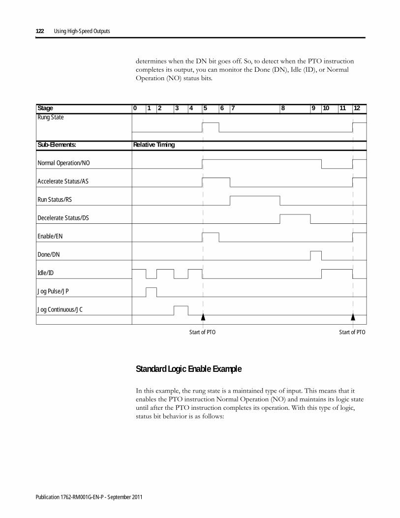
122 Using High-Speed Outputs
determines when the DN bit goes off. So, to detect when the PTO instruction completes its output, you can monitor the Done (DN), Idle (ID), or Normal Operation (NO) status bits.
Standard Logic Enable Example
In this example, the rung state is a maintained type of input. This means that it enables the PTO instruction Normal Operation (NO) and maintains its logic state until after the PTO instruction completes its operation. With this type of logic, status bit behavior is as follows:
Stage 0 1 2 3 4 5 6 7 8 9 10 11 12Rung State
Sub-Elements: Relative Timing
Normal Operation/NO
Accelerate Status/AS
Run Status/RS
Decelerate Status/DS
Enable/EN
Done/DN
Idle/ID
Jog Pulse/JP
Jog Continuous/JC
Start of PTO Start of PTO
Publication 1762-RM001G-EN-P - September 2011

Using High-Speed Outputs 123
The Done (DN) bit becomes true (1) when the PTO completes and remains set until the PTO rung logic is false. The false rung logic re-activates the PTO instruction. To detect when the PTO instruction completes its output, monitor the done (DN) bit.
Pulse Train Outputs (PTO) Function File
Within the RSLogix 500 Function File Folder, you see a PTO Function File with two elements, PTO0 (1762-L24BXB, 1762-L40BXB, and 1764-28BXB) and PTO1 (1764-28BXB only). These elements provide access to PTO configuration data and also allow the control program access to all information pertaining to each of the Pulse Train Outputs.
Stage 0 1 2 3 4 5 6 7 8 9 10 11 12Rung State
Sub-Elements: Relative Timing
Normal Operation /NO
Accelerate Status /AS
Run Status /RS
Decelerate Status /DS
Enable /EN
Done /DN
Idle /ID
Jog Pulse /JP
Jog Continuous /JC
Start of PTO Start of PTO
TIP If the controller mode is run, the data within sub-element fields may be changing.
Publication 1762-RM001G-EN-P - September 2011
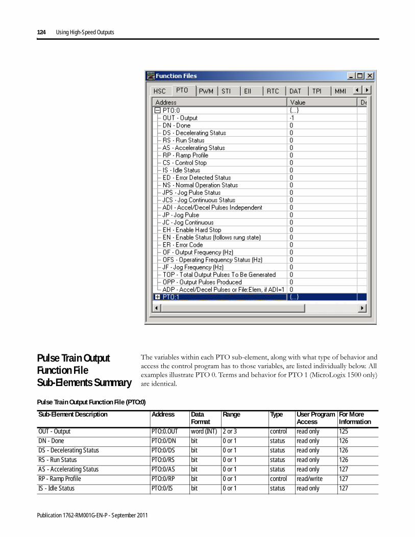
124 Using High-Speed Outputs
Pulse Train Output Function File Sub-Elements Summary
The variables within each PTO sub-element, along with what type of behavior and access the control program has to those variables, are listed individually below. All examples illustrate PTO 0. Terms and behavior for PTO 1 (MicroLogix 1500 only) are identical.
Pulse Train Output Function File (PTO:0)
Sub-Element Description Address Data Format
Range Type User Program Access
For More Information
OUT - Output PTO:0.OUT word (INT) 2 or 3 control read only 125DN - Done PTO:0/DN bit 0 or 1 status read only 126DS - Decelerating Status PTO:0/DS bit 0 or 1 status read only 126RS - Run Status PTO:0/RS bit 0 or 1 status read only 126AS - Accelerating Status PTO:0/AS bit 0 or 1 status read only 127RP - Ramp Profile PTO:0/RP bit 0 or 1 control read/write 127IS - Idle Status PTO:0/IS bit 0 or 1 status read only 127
Publication 1762-RM001G-EN-P - September 2011

Using High-Speed Outputs 125
PTO Output (OUT)
The PTO OUT (Output) variable defines the output (O0:0/2 or O0:0/3) that the PTO instruction controls. This variable is set within the function file folder when the control program is written and cannot be set by the user program.
• When OUT = 2, PTO pulses output 2 (O0:0.0/2) of the embedded outputs (1762-L24BXB, 1762-L40BXB, and 1764-28BXB).
• When OUT = 3, PTO pulses output 3 (O0:0.0/3) of the embedded outputs (1764-28BXB only).
ED - Error Detected Status PTO:0/ED bit 0 or 1 status read only 128NS - Normal Operation Status PTO:0/NS bit 0 or 1 status read only 128JPS - Jog Pulse Status PTO:0/JPS bit 0 or 1 status read only 134JCS - Jog Continuous Status PTO:0/JCS bit 0 or 1 status read only 135ADI - Accel/Decel Pulses Independent PTO:0/ADI bit 0 or 1 control read/write 131JP - Jog Pulse PTO:0/JP bit 0 or 1 control read/write 134JC - Jog Continuous PTO:0/JC bit 0 or 1 control read/write 135EH - Enable Hard Stop PTO:0/EH bit 0 or 1 control read/write 129EN - Enable Status (follows rung state) PTO:0/EN bit 0 or 1 status read only 129ER - Error Code PTO:0.ER word (INT) -2 to 7 status read only 136OF - Output Frequency (Hz) PTO:0.OF word (INT) 0 to 20,000 control read/write 129OFS - Operating Frequency Status (Hz) PTO:0.OFS word (INT) 0 to 20,000 status read only 130JF - Jog Frequency (Hz) PTO:0.JF word (INT) 0 to 20,000 control read/write 134TOP - Total Output Pulses To Be Generated PTO:0.TOP long word
(32-bit INT)0 to 2,147,483,647
control read/write 130
OPP - Output Pulses Produced PTO:0.OPP long word (32-bit INT)
0 to 2,147,483,647
status read only 130
ADP - Accel/Decel Pulses PTO:0.ADP long word (32-bit INT)
see p. 131 control read/write 131
CS - Controlled Stop PTO:0/CS bit 0 or 1 control read/write 133
Pulse Train Output Function File (PTO:0)
Sub-Element Description Address Data Format
Range Type User Program Access
For More Information
Sub-Element Description
Address Data Format Range Type User Program Access
OUT - Output PTO:0.OUT word (INT) 2 or 3 control read only
TIP Forcing an output controlled by the PTO while it is running stops all output pulses and causes a PTO error.
Publication 1762-RM001G-EN-P - September 2011

126 Using High-Speed Outputs
PTO Done (DN)
The PTO DN (Done) bit is controlled by the PTO sub-system. It can be used by an input instruction on any rung within the control program. The DN bit operates as follows:
• Set (1) - Whenever a PTO instruction has completed its operation successfully.
• Cleared (0) - When the rung the PTO is on is false. If the rung is false when the PTO instruction completes, the Done bit is set until the next scan of the PTO instruction.
PTO Decelerating Status (DS)
The PTO DS (Decel) bit is controlled by the PTO sub-system. It can be used by an input instruction on any rung within the control program. The DS bit operates as follows:
• Set (1) - Whenever a PTO instruction is within the deceleration phase of the output profile.
• Cleared (0) - Whenever a PTO instruction is not within the deceleration phase of the output profile.
PTO Run Status (RS)
The PTO RS (Run Status) bit is controlled by the PTO sub-system. It can be used by an input instruction on any rung within the control program. The RS bit operates as follows:
• Set (1) - Whenever a PTO instruction is within the run phase of the output profile.
Sub-Element Description
Address Data Format Range Type User Program Access
DN - Done PTO:0/DN bit 0 or 1 status read only
Sub-Element Description
Address Data Format Range Type User Program Access
DS - Decelerating Status PTO:0/DS bit 0 or 1 status read only
Sub-Element Description
Address Data Format Range Type User Program Access
RS - Run Status PTO:0/RS bit 0 or 1 status read only
Publication 1762-RM001G-EN-P - September 2011

Using High-Speed Outputs 127
• Cleared (0) - Whenever a PTO instruction is not within the run phase of the output profile.
PTO Accelerating Status (AS)
The PTO AS (Accelerating Status) bit is controlled by the PTO sub-system. It can be used by an input instruction on any rung within the control program. The AS bit operates as follows:
• Set (1) - Whenever a PTO instruction is within the acceleration phase of the output profile.
• Cleared (0) - Whenever a PTO instruction is not within the acceleration phase of the output profile.
PTO Ramp Profile (RP)
The PTO RP (Ramp Profile) bit controls how the output pulses generated by the PTO sub-system accelerate to and decelerate from the Output Frequency that is set in the PTO function file (PTO:0.OF). It can be used by an input or output instruction on any rung within the control program. The RP bit operates as follows:
• Set (1) - Configures the PTO instruction to produce an S-Curve profile.• Cleared (0) - Configures the PTO instruction to produce a Trapezoid profile.
PTO Idle Status (IS)
Sub-Element Description
Address Data Format
Range Type User Program Access
AS - Accelerating Status PTO:0/AS bit 0 or 1 status read only
Sub-Element Description
Address Data Format Range Type User Program Access
RP - Ramp Profile PTO:0/RP bit 0 or 1 control read/write
Sub-Element Description
Address Data Format Range Type User Program Access
IS - Idle Status PTO:0/IS bit 0 or 1 status read only
Publication 1762-RM001G-EN-P - September 2011

128 Using High-Speed Outputs
The PTO IS (Idle Status) is controlled by the PTO sub-system. It can be used in the control program by an input instruction. The PTO sub-system must be in an idle state whenever any PTO operation needs to start.
The IS bit operates as follows:
• Set (1) - PTO sub-system is in an idle state. The idle state is defined as the PTO is not running and no errors are present.
• Cleared (0) - PTO sub-system is not in an idle state (it is running)
PTO Error Detected (ED)
The PTO ED (Error Detected Status) bit is controlled by the PTO sub-system. It can be used by an input instruction on any rung within the control program to detect when the PTO instruction is in an error state. If an error state is detected, the specific error is identified in the error code register (PTO:0.ER). The ED bit operates as follows:
• Set (1) - Whenever a PTO instruction is in an error state • Cleared (0) - Whenever a PTO instruction is not in an error state
PTO Normal Operation Status (NS)
The PTO NS (Normal Operation Status) bit is controlled by the PTO sub-system. It can be used by an input instruction on any rung within the control program to detect when the PTO is in its normal state. A normal state is ACCEL, RUN, DECEL or DONE, with no PTO errors. The NS bit operates as follows:
• Set (1) - Whenever a PTO instruction is in its normal state • Cleared (0) - Whenever a PTO instruction is not in its normal state
Sub-Element Description
Address Data Format Range Type User Program Access
ED - Error Detected Status PTO:0/ED bit 0 or 1 status read only
Sub-Element Description Address Data Format Range Type User Program Access
NS - Normal Operation Status PTO:0/NS bit 0 or 1 status read only
Publication 1762-RM001G-EN-P - September 2011

Using High-Speed Outputs 129
PTO Enable Hard Stop (EH)
The PTO EH (Enable Hard Stop) bit is used to stop the PTO sub-system immediately. Once the PTO sub-system starts a pulse sequence, the only way to stop generating pulses is to set the enable hard stop bit. The enable hard stop aborts any PTO sub-system operation (idle, normal, jog continuous or jog pulse) and generates a PTO sub-system error. The EH bit operates as follows:
• Set (1) - Instructs the PTO sub-system to stop generating pulses immediately (output off = 0)
• Cleared (0) - Normal operation
PTO Enable Status (EN)
The PTO EN (Enable Status) is controlled by the PTO sub-system. When the rung preceding the PTO instruction is solved true, the PTO instruction is enabled and the enable status bit is set. If the rung preceding the PTO instruction transitions to a false state before the pulse sequence completes its operation, the enable status bit resets (0). The EN bit operates as follows:
• Set (1) - PTO is enabled• Cleared (0) - PTO has completed, or the rung preceding the PTO is false
PTO Output Frequency (OF)
The PTO OF (Output Frequency) variable defines the frequency of the PTO output during the RUN phase of the pulse profile. This value is typically determined by the type of device that is being driven, the mechanics of the application, or the device/components being moved. Data less than zero and greater than 20,000 generates a PTO error.
Sub-Element Description
Address Data Format Range Type User Program Access
EH - Enable Hard Stop PTO:0/EH bit 0 or 1 control read/write
Sub-Element Description
Address Data Format Range Type User Program Access
EN - Enable Status (follows rung state)
PTO:0/EN bit 0 or 1 status read only
Sub-Element Description Address Data Format
Range Type User Program Access
OF - Output Frequency (Hz) PTO:0.OF word (INT) 0 to 20,000 control read/write
Publication 1762-RM001G-EN-P - September 2011
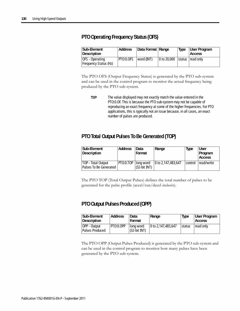
130 Using High-Speed Outputs
PTO Operating Frequency Status (OFS)
The PTO OFS (Output Frequency Status) is generated by the PTO sub-system and can be used in the control program to monitor the actual frequency being produced by the PTO sub-system.
PTO Total Output Pulses To Be Generated (TOP)
The PTO TOP (Total Output Pulses) defines the total number of pulses to be generated for the pulse profile (accel/run/decel inclusive).
PTO Output Pulses Produced (OPP)
The PTO OPP (Output Pulses Produced) is generated by the PTO sub-system and can be used in the control program to monitor how many pulses have been generated by the PTO sub-system.
Sub-Element Description
Address Data Format Range Type User Program Access
OFS - Operating Frequency Status (Hz)
PTO:0.OFS word (INT) 0 to 20,000 status read only
TIP The value displayed may not exactly match the value entered in the PTO:0.OF. This is because the PTO sub-system may not be capable of reproducing an exact frequency at some of the higher frequencies. For PTO applications, this is typically not an issue because, in all cases, an exact number of pulses are produced.
Sub-Element Description
Address Data Format
Range Type User Program Access
TOP - Total Output Pulses To Be Generated
PTO:0.TOP long word (32-bit INT)
0 to 2,147,483,647 control read/write
Sub-Element Description
Address Data Format
Range Type User Program Access
OPP - Output Pulses Produced
PTO:0.OPP long word (32-bit INT)
0 to 2,147,483,647 status read only
Publication 1762-RM001G-EN-P - September 2011

Using High-Speed Outputs 131
PTO Accel/Decel Pulses Independent (ADI)
The PTO ADI (Accel/Decel Pulses Independent) bit is used to define whether the acceleration and deceleration intervals will be the same, or if each will have a unique value. When this bit is set (1), separate profiles are used. When this bit is clear (0), the PTO will operate with the deceleration profile as a mirror of the acceleration profile.
If separate acceleration and deceleration profiles are desired, you must choose a long integer file number and a starting element. There must be four long elements available in the file:
The choice of selecting a common profile or separate profiles must be made at the time of programming. This cannot be changed once the program is downloaded into the controller. The selection of the ramp type must be made prior to going to run. The acceleration and deceleration counts must be entered before the PTO is enabled. If the four long elements are not properly identified, the controller will return a -3 error in the PTO function file when going to run.
PTO Accel / Decel Pulses or File:Elem, if ADI=1 (ADP)
The PTO ADP (Accel/Decel Pulses) defines how many of the total pulses (TOP variable) will be applied to each of the ACCEL and DECEL components. The ADP will determine the acceleration and deceleration rate from 0 to the PTO Output Frequency (OF). The PTO Output Frequency (OF) defines the operating frequency in pulses/second during the run portion of the profile.
Sub-Element Description
Address Data Format Range Type User Program Access
ADI - Accel/Decel Pulses Independent
PTO:0/ADI bit 0 or 1 control read/write
Element 1: Acceleration Count
Element 2: Deceleration Count
Elements 3 and 4: reserved
Sub-Element Description
Address Data Format Range Type User Program Access
ADP - Accel/Decel Pulses
PTO:0.ADP long word (32-bit INT)
see below control read/write
Publication 1762-RM001G-EN-P - September 2011

132 Using High-Speed Outputs
In the example below,
• TOP (total output pulses) = 12,000• ADP (accelerate/decelerate pulses)= 6,000 (This is the maximum ADP
value that may be entered without causing a fault. The run portion will equal 0.)
In this example, the maximum value that could be used for accelerate/decelerate is 6000, because if both accelerate and decelerate are 6000, the total number of pulses = 12,000. The run component would be zero. This profile would consist of an acceleration phase from 0 to 6000. At 6000, the output frequency (OF variable) is generated and immediately enters the deceleration phase, 6000 to 12,000. At 12,000, the PTO operation would stop (output frequency = 0).
If you need to determine the ramp period (accelerate/decelerate ramp duration):
• 2 x ADP/OF = duration in seconds (OF = output frequency)
The following formulas can be used to calculate the maximum frequency limit for both profiles. The maximum frequency = the integer which is less than or equal to the result found below (OF = output frequency):
• For Trapezoid Profiles: [OF x (OF/4)] + 0.5• For S-Curve Profiles: 0.999 x OF x SQRT(OF/6)
TIP When entering the ADP parameters, the PTO will generate an Accel/Decel Error if one of the following conditions occur:
″ The total pulses for the acceleration and deceleration phases is less than 0.
″ The total pulses for the acceleration and deceleration phases is greater than the total output pulses to be generated (TOP).
Acceleration and deceleration values can either be identical (ADI = 0), or a unique value for each (ADI = 1).
Accel Run Decel
6,000 0 6,000
Accel Run Decel
12,000
Publication 1762-RM001G-EN-P - September 2011
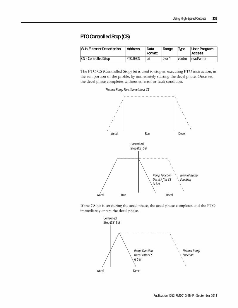
Using High-Speed Outputs 133
PTO Controlled Stop (CS)
The PTO CS (Controlled Stop) bit is used to stop an executing PTO instruction, in the run portion of the profile, by immediately starting the decel phase. Once set, the decel phase completes without an error or fault condition.
If the CS bit is set during the accel phase, the accel phase completes and the PTO immediately enters the decel phase.
Sub-Element Description Address Data Format
Range Type User Program Access
CS - Controlled Stop PTO:0/CS bit 0 or 1 control read/write
Normal Ramp Function without CS
Accel Run Decel
Normal Ramp Function
Ramp Function Decel After CS is Set
Accel
Controlled Stop (CS) Set
Run Decel
Normal Ramp Function
Ramp Function Decel After CS is Set
Accel
Controlled Stop (CS) Set
Decel
Publication 1762-RM001G-EN-P - September 2011

134 Using High-Speed Outputs
PTO Jog Frequency (JF)
The PTO JF (Jog Frequency) variable defines the frequency of the PTO output during all Jog phases. This value is typically determined by the type of device that is being driven, the mechanics of the application, or the device/components being moved). Data less than zero and greater than 20,000 generates a PTO error.
PTO Jog Pulse (JP)
The PTO JP (Jog Pulse) bit is used to instruct the PTO sub-system to generate a single pulse. The width is defined by the Jog Frequency parameter in the PTO function file. Jog Pulse operation is only possible under the following conditions:
• PTO sub-system in idle• Jog continuous not active• Enable not active
The JP bit operates as follows:
• Set (1) - Instructs the PTO sub-system to generate a single Jog Pulse• Cleared (0) - Arms the PTO Jog Pulse sub-system
PTO Jog Pulse Status (JPS)
The PTO JPS (Jog Pulse Status) bit is controlled by the PTO sub-system. It can be used by an input instruction on any rung within the control program to detect when the PTO has generated a Jog Pulse.
Sub-Element Description
Address Data Format
Range Type User Program Access
JF - Jog Frequency (Hz) PTO:0.JF word (INT) 0 to 20,000 control read/write
Sub-Element Description
Address Data Format Range Type User Program Access
JP - Jog Pulse PTO:0/JP bit 0 or 1 control read/write
Sub-Element Description
Address Data Format
Range Type User Program Access
JPS - Jog Pulse Status PTO:0/JPS bit 0 or 1 status read only
Publication 1762-RM001G-EN-P - September 2011
Using High-Speed Outputs 135
The JPS bit operates as follows:
• Set (1) - Whenever a PTO instruction outputs a Jog Pulse• Cleared (0) - Whenever a PTO instruction exits the Jog Pulse state
PTO Jog Continuous (JC)
The PTO JC (Jog Continuous) bit instructs the PTO sub-system to generate continuous pulses. The frequency generated is defined by the Jog Frequency parameter in the PTO function file. Jog Continuous operation is only possible under the following conditions:
• PTO sub-system in idle• Jog Pulse not active• Enable not active
The JC bit operates as follows:
• Set (1) - Instructs the PTO sub-system to generate continuous Jog Pulses• Cleared (0) - The PTO sub-system does not generate Jog Pulses
When the Jog Continuous bit is cleared, the current output pulse is truncated.
PTO Jog Continuous Status (JCS)
The PTO JCS (Jog Continuous Status) bit is controlled by the PTO sub-system. It can be used by an input instruction on any rung within the control program to detect when the PTO is generating continuous Jog Pulses. The JCS bit operates as follows:
• Set (1) - Whenever a PTO instruction is generating continuous Jog Pulses• Cleared (0) - Whenever a PTO instruction is not generating continuous Jog
Pulses.
TIP The output (jog) pulse is normally complete with the JP bit set. The JPS bit remains set until the JP bit is cleared (0 = off).
Sub-Element Description
Address Data Format Range Type User Program Access
JC - Jog Continuous PTO:0/JC bit 0 or 1 control read/write
Sub-Element Description Address Data Format
Range Type User Program Access
JCS - Jog Continuous Status PTO:0/JCS bit 0 or 1 status read only
Publication 1762-RM001G-EN-P - September 2011
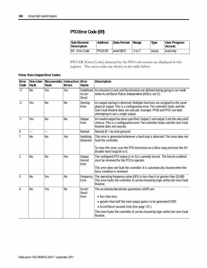
136 Using High-Speed Outputs
PTO Error Code (ER)
PTO ER (Error Codes) detected by the PTO sub-system are displayed in this register. The error codes are shown in the table below:
Sub-Element Description
Address Data Format Range Type User Program Access
ER - Error Code PTO:0.ER word (INT) -3 to 7 status read only
Pulse Train Output Error Codes
Error Code
Non-User Fault
Recoverable Fault
Instruction Errors
Error Name
Description
-3 No Yes Yes Undefined Accel/Decel
Acceleration Count and Deceleration not defined during going to run mode when Accel/Decel Pulses Independent (ADI) is set (1).
-2 Yes No No Overlap Error
An output overlap is detected. Multiple functions are assigned to the same physical output. This is a configuration error. The controller faults and the User Fault Routine does not execute. Example: PTO0 and PTO1 are both attempting to use a single output.
-1 Yes No No Output Error
An invalid output has been specified. Output 2 and output 3 are the only valid choices. This is a configuration error. The controller faults and the User Fault Routine does not execute.
0 --- --- Normal Normal (0 = no error present)
1 No No Yes Hardstop Detected
This error is generated whenever a hard stop is detected. This error does not fault the controller.
To clear this error, scan the PTO instruction on a false rung and reset the EH (Enable Hard Stop) bit to 0.
2 No No Yes Output Forced Error
The configured PTO output (2 or 3) is currently forced. The forced condition must be removed for the PTO to operate.
This error does not fault the controller. It is automatically cleared when the force condition is removed.
3 No Yes No Frequency Error
The operating frequency value (OFS) is less than 0 or greater than 20,000. This error faults the controller. It can be cleared by logic within the User Fault Routine.
4 No Yes No Accel/Decel Error
The accelerate/decelerate parameters (ADP) are:
• less than zero
• greater than half the total output pulses to be generated (TOP)
• Accel/Decel exceeds limit (See page 131.)
This error faults the controller. It can be cleared by logic within the User Fault Routine.
Publication 1762-RM001G-EN-P - September 2011

Using High-Speed Outputs 137
PWM - Pulse Width Modulation
Instruction Type: output
PWM Function The PWM function allows a field device to be controlled by a PWM wave form. The PWM profile has two primary components:
• Frequency to be generated• Duty Cycle interval
The PWM instruction, along with the HSC and PTO functions, are different than all other controller instructions. Their operation is performed by custom circuitry that runs in parallel with the main system processor. This is necessary because of the high performance requirements of these instructions.
5 No No Yes Jog Error PTO is in the idle state and two or more of the following are set:
• Enable (EN) bit set
• Jog Pulse (JP) bit set
• Jog Continuous (JC) bit set
This error does not fault the controller. It is automatically cleared when the error condition is removed.
6 No Yes No Jog Frequency Error
The jog frequency (JF) value is less than 0 or greater than 20,000. This error faults the controller. It can be cleared by logic within the User Fault Routine.
7 No Yes No Length Error
The total output pulses to be generated (TOP) is less than zero. This error faults the controller. It can be cleared by logic within the User Fault Routine.
Pulse Train Output Error Codes
Error Code
Non-User Fault
Recoverable Fault
Instruction Errors
Error Name
Description
PWMPulse Width ModulationPWM Number 1
PWM
IMPORTANT The PWM function can only be used with the controller’s embedded I/O. It cannot be used with expansion I/O modules.
IMPORTANT The PWM instruction should only be used with MicroLogix 1200 and 1500 BXB units. Relay outputs are not capable of performing very high-speed operations.
Execution Time for the PWM Instruction
Controller When Rung Is:True False
MicroLogix 1200 126.6 μs 24.7 μsMicroLogix 1500 107.4 μs 21.1 μs
Publication 1762-RM001G-EN-P - September 2011
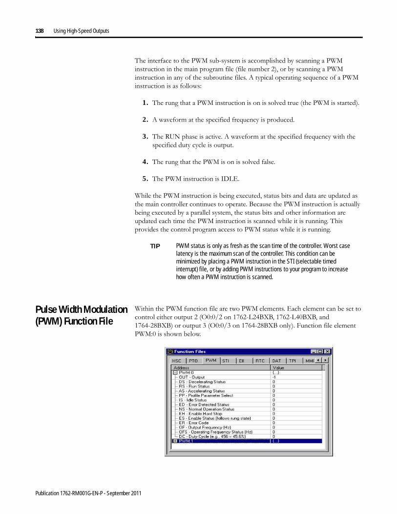
138 Using High-Speed Outputs
The interface to the PWM sub-system is accomplished by scanning a PWM instruction in the main program file (file number 2), or by scanning a PWM instruction in any of the subroutine files. A typical operating sequence of a PWM instruction is as follows:
1. The rung that a PWM instruction is on is solved true (the PWM is started).
2. A waveform at the specified frequency is produced.
3. The RUN phase is active. A waveform at the specified frequency with the specified duty cycle is output.
4. The rung that the PWM is on is solved false.
5. The PWM instruction is IDLE.
While the PWM instruction is being executed, status bits and data are updated as the main controller continues to operate. Because the PWM instruction is actually being executed by a parallel system, the status bits and other information are updated each time the PWM instruction is scanned while it is running. This provides the control program access to PWM status while it is running.
Pulse Width Modulation (PWM) Function File
Within the PWM function file are two PWM elements. Each element can be set to control either output 2 (O0:0/2 on 1762-L24BXB, 1762-L40BXB, and 1764-28BXB) or output 3 (O0:0/3 on 1764-28BXB only). Function file element PWM:0 is shown below.
TIP PWM status is only as fresh as the scan time of the controller. Worst case latency is the maximum scan of the controller. This condition can be minimized by placing a PWM instruction in the STI (selectable timed interrupt) file, or by adding PWM instructions to your program to increase how often a PWM instruction is scanned.
Publication 1762-RM001G-EN-P - September 2011
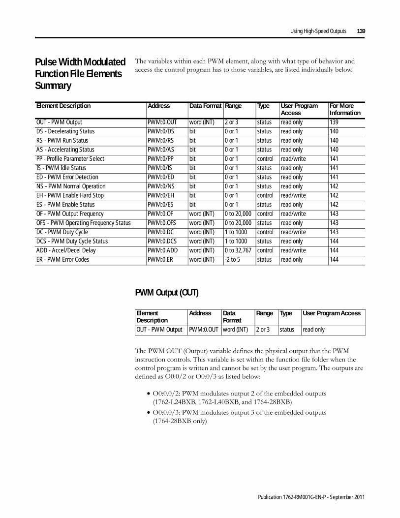
Using High-Speed Outputs 139
Pulse Width Modulated Function File Elements Summary
The variables within each PWM element, along with what type of behavior and access the control program has to those variables, are listed individually below.
PWM Output (OUT)
The PWM OUT (Output) variable defines the physical output that the PWM instruction controls. This variable is set within the function file folder when the control program is written and cannot be set by the user program. The outputs are defined as O0:0/2 or O0:0/3 as listed below:
• O0:0.0/2: PWM modulates output 2 of the embedded outputs (1762-L24BXB, 1762-L40BXB, and 1764-28BXB)
• O0:0.0/3: PWM modulates output 3 of the embedded outputs (1764-28BXB only)
Element Description Address Data Format Range Type User Program Access
For More Information
OUT - PWM Output PWM:0.OUT word (INT) 2 or 3 status read only 139DS - Decelerating Status PWM:0/DS bit 0 or 1 status read only 140RS - PWM Run Status PWM:0/RS bit 0 or 1 status read only 140AS - Accelerating Status PWM:0/AS bit 0 or 1 status read only 140PP - Profile Parameter Select PWM:0/PP bit 0 or 1 control read/write 141IS - PWM Idle Status PWM:0/IS bit 0 or 1 status read only 141ED - PWM Error Detection PWM:0/ED bit 0 or 1 status read only 141NS - PWM Normal Operation PWM:0/NS bit 0 or 1 status read only 142EH - PWM Enable Hard Stop PWM:0/EH bit 0 or 1 control read/write 142ES - PWM Enable Status PWM:0/ES bit 0 or 1 status read only 142OF - PWM Output Frequency PWM:0.OF word (INT) 0 to 20,000 control read/write 143OFS - PWM Operating Frequency Status PWM:0.OFS word (INT) 0 to 20,000 status read only 143DC - PWM Duty Cycle PWM:0.DC word (INT) 1 to 1000 control read/write 143DCS - PWM Duty Cycle Status PWM:0.DCS word (INT) 1 to 1000 status read only 144ADD - Accel/Decel Delay PWM:0.ADD word (INT) 0 to 32,767 control read/write 144ER - PWM Error Codes PWM:0.ER word (INT) -2 to 5 status read only 144
Element Description
Address Data Format
Range Type User Program Access
OUT - PWM Output PWM:0.OUT word (INT) 2 or 3 status read only
Publication 1762-RM001G-EN-P - September 2011
140 Using High-Speed Outputs
PWM Decelerating Status (DS)
The PWM DS (Decel) bit is controlled by the PWM sub-system. It can be used by an input instruction on any rung within the control program. The DS bit operates as follows:
• Set (1) - Whenever a PWM output is within the deceleration phase of the output profile.
• Cleared (0) - Whenever a PWM output is not within the deceleration phase of the output profile.
PWM Run Status (RS)
The PWM RS (Run Status) bit is controlled by the PWM sub-system. It can be used by an input instruction on any rung within the control program.
• Set (1) - Whenever the PWM instruction is within the run phase of the output profile.
• Cleared (0) - Whenever the PWM instruction is not within the run phase of the output profile.
PWM Accelerating Status (AS)
The PWM AS (Accelerating Status) bit is controlled by the PWM sub-system. It can be used by an input instruction on any rung within the control program. The AS bit operates as follows:
• Set (1) - Whenever a PWM output is within the acceleration phase of the output profile.
• Cleared (0) - Whenever a PWM output is not within the acceleration phase of the output profile.
Element Description Address Data Format Range Type User Program Access
DS - Decelerating Status PWM:0/DS bit 0 or 1 status read only
Element Description Address Data Format Range Type User Program Access
RS - PWM Run Status PWM:0/RS bit 0 or 1 status read only
Element Description Address Data Format Range Type User Program Access
AS - Accelerating Status PWM:0/AS bit 0 or 1 status read only
Publication 1762-RM001G-EN-P - September 2011
Using High-Speed Outputs 141
PWM Profile Parameter Select (PP)
The PWM PP (Profile Parameter Select) selects which component of the waveform is modified during a ramp phase:
• Set (1) - selects Frequency• Cleared (0) - selects Duty Cycle
The PWM PP bit cannot be modified while the PWM output is running/enabled. See PWM ADD on page 144 for more information.
PWM Idle Status (IS)
The PWM IS (Idle Status) is controlled by the PWM sub-system and represents no PWM activity. It can be used in the control program by an input instruction.
• Set (1) - PWM sub-system is in an idle state.• Cleared (0) - PWM sub-system is not in an idle state (it is running).
PWM Error Detected (ED)
The PWM ED (Error Detected) bit is controlled by the PWM sub-system. It can be used by an input instruction on any rung within the control program to detect when the PWM instruction is in an error state. If an error state is detected, the specific error is identified in the error code register (PWM:0.ED).
• Set (1) - Whenever a PWM instruction is in an error state. • Cleared (0) - Whenever a PWM instruction is not in an error state.
Element Description Address Data Format Range Type User Program Access
PP - Profile Parameter Select PWM:0/PP bit 0 or 1 control read/write
Element Description Address Data Format Range Type User Program Access
IS - PWM Idle Status PWM:0/IS bit 0 or 1 status read only
Element Description Address Data Format
Range Type User Program Access
ED - PWM Error Detection PWM:0/ED bit 0 or 1 status read only
Publication 1762-RM001G-EN-P - September 2011

142 Using High-Speed Outputs
PWM Normal Operation (NS)
The PWM NS (Normal Operation) bit is controlled by the PWM sub-system. It can be used by an input instruction on any rung within the control program to detect when the PWM is in its normal state. A normal state is defined as ACCEL, RUN, or DECEL with no PWM errors.
• Set (1) - Whenever a PWM instruction is in its normal state. • Cleared (0) - Whenever a PWM instruction is not in its normal state.
PWM Enable Hard Stop (EH)
The PWM EH (Enable Hard Stop) bit stops the PWM sub-system immediately. A PWM hard stop generates a PWM sub-system error.
• Set (1) - Instructs the PWM sub-system to stop its output modulation immediately (output off = 0).
• Cleared (0) - Normal operation.
PWM Enable Status (ES)
The PWM ES (Enable Status) is controlled by the PWM sub-system. When the rung preceding the PWM instruction is solved true, the PWM instruction is enabled, and the enable status bit is set. When the rung preceding the PWM instruction transitions to a false state, the enable status bit is reset (0) immediately.
• Set (1) - PWM is enabled.• Cleared (0) - PWM has completed or the rung preceding the PWM is false.
Element Description Address Data Format
Range Type User Program Access
NS - PWM Normal Operation PWM:0/NS bit 0 or 1 status read only
Element Description Address Data Format
Range Type User Program Access
EH - PWM Enable Hard Stop PWM:0/EH bit 0 or 1 control read/write
Element Description Address Data Format Range Type User Program Access
ES - PWM Enable Status PWM:0/ES bit 0 or 1 status read only
Publication 1762-RM001G-EN-P - September 2011

Using High-Speed Outputs 143
PWM Output Frequency (OF)
The PWM OF (Output Frequency) variable defines the frequency of the PWM function. This frequency can be changed at any time.
PWM Operating Frequency Status (OFS)
The PWM OFS (Output Frequency Status) is generated by the PWM sub-system and can be used in the control program to monitor the actual frequency produced by the PWM sub-system.
PWM Duty Cycle (DC)
The PWM DC (Duty Cycle) variable controls the output signal produced by the PWM sub-system. Changing this variable in the control program changes the output waveform. Typical values and output waveform:
• DC = 1000: 100% Output ON (constant, no waveform)• DC = 750: 75% Output ON, 25% output OFF• DC = 500: 50% Output ON, 50% output OFF• DC = 250: 25% Output ON, 75% output OFF• DC = 0: 0% Output OFF (constant, no waveform)
Element Description Address Data Format
Range Type User Program Access
OF - PWM Output Frequency PWM:0.OF word (INT) 0 to 20,000 control read/write
Element Description Address Data Format
Range Type User Program Access
OFS - PWM Operating Frequency Status
PWM:0.OFS word (INT) 0 to 20,000 status read only
Element Description Address Data Format Range Type User Program Access
DC - PWM Duty Cycle PWM:0.DC word (INT) 1 to 1000 control read/write
Publication 1762-RM001G-EN-P - September 2011

144 Using High-Speed Outputs
PWM Duty Cycle Status (DCS)
The PWM DCS (Duty Cycle Status) provides feedback from the PWM sub-system. The Duty Cycle Status variable can be used within an input instruction on a rung of logic to provide PWM system status to the remaining control program.
PWM Accel/Decel Delay (ADD)
PWM ADD (Accel/Decel Delay) defines the amount of time in 10 millisecond intervals to ramp from zero to the specified frequency or duration. Also specifies the time to ramp down to zero.
The PWM ADD value is loaded and activated immediately (whenever the PWM instruction is scanned on a true rung of logic). This allows multiple steps or stages of acceleration or deceleration to occur.
PWM Error Code (ER)
PWM ER (Error Codes) detected by the PWM sub-system are displayed in this register. The table identifies known errors.
Element Description Address Data Format
Range Type User Program Access
DCS - PWM Duty Cycle Status PWM:0.DCS word (INT) 1 to 1000 status read only
Element Description Address Data Format Range Type User Program Access
ADD - Accel/Decel Delay PWM:0.ADD word (INT) 0 to 32,767 control read/write
Element Description Address Data Format Range Type User Program Access
ER - PWM Error Codes PWM:0.ER word (INT) -2 to 5 status read only
Error Code
Non-User Fault
Recoverable Fault
Instruction Errors
Error Name
Description
-2 Yes No No Overlap Error
An output overlap is detected. Multiple functions are assigned to the same physical output. This is a configuration error. The controller faults and the User Fault Routine does not execute. Example: PWM0 and PWM1 are both attempting to use a single output.
-1 Yes No No Output Error
An invalid output has been specified. Output 2 and output 3 are the only valid choices. This is a configuration error. The controller faults and the User Fault Routine does not execute.
0 Normal Normal (0 = no error present)
Publication 1762-RM001G-EN-P - September 2011

Using High-Speed Outputs 145
1 No No Yes Hardstop Error
This error is generated whenever a hardstop is detected. This error does not fault the controller. It is automatically cleared when the hardstop condition is removed.
2 No No Yes Output Forced Error
The configured PWM output (2 or 3) is currently forced. The forced condition must be removed for the PWM to operate. This error does not fault the controller. It is automatically cleared when the force condition is removed.
3 Yes Yes No Frequency Error
The frequency value is less than 0 or greater than 20,000. This error faults the controller. It can be cleared by logic within the User Fault Routine.
4 Reserved5 Yes Yes No Duty Cycle
ErrorThe PWM duty cycle is either less than zero or greater than 1000.
This error faults the controller. It can be cleared by logic within the User Fault Routine.
Publication 1762-RM001G-EN-P - September 2011

146 Using High-Speed Outputs
Notes:
Publication 1762-RM001G-EN-P - September 2011

Chapter 7
Relay-Type (Bit) Instructions
Use relay-type (bit) instructions to monitor and/or control bits in a data file or function file, such as input bits or timer control-word bits. The following instructions are described in this chapter:
These instructions operate on a single bit of data. During operation, the processor may set or reset the bit, based on logical continuity of ladder rungs. You can address a bit as many times as your program requires.
XIC - Examine if ClosedXIO - Examine if Open
Instruction Type: input
Use the XIC instruction to determine if the addressed bit is on. Use the XIO instruction to determine if the addressed bit is off.
When used on a rung, the bit address being examined can correspond to the status of real world input devices connected to the base unit or expansion I/O, or internal addresses (data or function files). Examples of devices that turn on or off:
• a push button wired to an input (addressed as I1:0/4)• an output wired to a pilot light (addressed as O0:0/2)• a timer controlling a light (addressed as T4:3/DN)• a bit in the bit file (addressed as B3/16)
Instruction Used To: PageXIC - Examine if Closed Examine a bit for an ON condition 147XIO - Examine if Open Examine a bit for an OFF condition 147OTE - Output Enable Turn ON or OFF a bit (non-retentive) 148OTL - Output Latch Latch a bit ON (retentive) 149OTU - Output Unlatch Unlatch a bit OFF (retentive) 149ONS - One Shot Detect an OFF to ON transition 150OSR - One Shot Rising Detect an OFF to ON transition 151OSF - One Shot Falling Detect an ON to OFF transition 151
B3:0
0
B3:0
0
Execution Time for the XIC and XIO Instructions
Controller When Instruction Is:True False
MicroLogix 1200 0.9 μs 0.8 μsMicroLogix 1500 0.9 μs 0.7 μs
147 Publication 1762-RM001G-EN-P - September 2011

148 Relay-Type (Bit) Instructions
The instructions operate as follows:
Addressing Modes and File Types can be used as shown in the following table:
OTE - Output EnergizeInstruction Type: output
Use an OTE instruction to turn a bit location on when rung conditions are evaluated as true and off when the rung is evaluated as false. An example of a device that turns on or off is an output wired to a pilot light (addressed as O0:0/4). OTE instructions are reset (turned OFF) when:
• You enter or return to the program or remote program mode or power is restored.
• The OTE is programmed within an inactive or false Master Control Reset (MCR) zone.
XIO and XIC Instruction Operation
Rung State Addressed Bit
XIC Instruction XIO Instruction
True Off Returns a False Returns a True
True On Returns a True Returns a False
False -- Instruction is not evaluated Instruction is not evaluated
XIC and XIO Instructions Valid Addressing Modes and File TypesFor definitions of the terms used in this table see Using the Instruction Descriptions on page 82.
Parameter
Data Files Function Files(1)
CS -
Com
ms
IOS
- I/O
DLS
- Dat
a Lo
g (2
) Address Mode(3) Address Level
O I S B T, C
, R
N F ST L MG
, PD
PLS
RTC
HSC
PTO
, PW
M
STI
EII
BHI
MM
I
DAT
TPI
Imm
edia
te
Dir
ect
Indi
rect
Bit
Wor
d
Long
Wor
d
Elem
ent
Operand Bit • • • • • • • • • • • • • • • • • • • • • • •
(1) DAT files are valid for the MicroLogix 1500 only. PTO and PWM files are only for use with MicroLogix 1200 and 1500 BXB units.
(2) The Data Log Status file can only be used by the MicroLogix 1500 1764-LRP Processor.
(3) See Important note about indirect addressing.
IMPORTANT You cannot use indirect addressing with: S, ST, MG, PD, RTC, HSC, PTO, PWM, STI, EII, BHI, MMI, DAT, TPI, CS, IOS, and DLS files.
B3:0
1Execution Time for the OTE Instructions
Controller When Rung Is:True False
MicroLogix 1200 1.4 μs 1.1 μsMicroLogix 1500 1.2 μs 0.0 μs
Publication 1762-RM001G-EN-P - September 2011

Relay-Type (Bit) Instructions 149
Addressing Modes and File Types can be used as shown in the following table:
OTL - Output LatchOTU - Output Unlatch
Instruction Type: output
The OTL and OTU instructions are retentive output instructions. OTL turns on a bit, while OTU turns off a bit. These instructions are usually used in pairs, with both instructions addressing the same bit.
TIP A bit that is set within a subroutine using an OTE instruction remains set until the OTE is scanned again.
ATTENTION: If you enable interrupts during the program scan via an OTL, OTE, or UIE, this instruction must be the last instruction executed on the rung (last instruction on last branch). It is recommended this be the only output instruction on the rung.
ATTENTION: Never use an output address at more than one place in your logic program. Always be fully aware of the load represented by the output coil.
OTE Instruction Valid Addressing Modes and File TypesFor definitions of the terms used in this table see Using the Instruction Descriptions on page 82.
Parameter
Data Files Function Files(1)
CS -
Com
ms
IOS
- I/O
DLS
- Da
ta L
og (2
) Address Mode(3) Address Level
O I S B T, C
, R
N F ST L MG
, PD
PLS
RTC
HSC
PTO
, PW
M
STI
EII
BHI
MM
I
DAT
TPI
Imm
edia
te
Dir
ect
Indi
rect
Bit
Wor
d
Long
Wor
d
Elem
ent
Destination Bit • • • • • • • • • • • • • • • • • •
(1) DAT files are valid for the MicroLogix 1500 only. PTO and PWM files are only for use with MicroLogix 1200 and 1500 BXB units.
(2) The Data Log Status file can only be used by the MicroLogix 1500 1764-LRP Processor.
(3) See Important note about indirect addressing.
IMPORTANT You cannot use indirect addressing with: S, ST, MG, PD, RTC, HSC, PTO, PWM, STI, EII, BHI, MMI, DAT, TPI, CS, IOS, and DLS files.
L B3:0
1
UB3:0
1
Execution Time for the OTL and OTU Instructions
Controller OTL - When Rung Is: OTU - When Rung Is:True False True False
MicroLogix 1200 1.0 μs 0.0 μs 1.1 μs 0.0 μsMicroLogix 1500 0.9 μs 0.0 μs 0.9 μs 0.0 μs
Publication 1762-RM001G-EN-P - September 2011

150 Relay-Type (Bit) Instructions
Since these are latching outputs, once set (or reset), they remain set (or reset) regardless of the rung condition.
Addressing Modes and File Types can be used as shown in the following table:
ONS - One ShotInstruction Type: input
ATTENTION: If you enable interrupts during the program scan via an OTL, OTE, or UIE, this instruction must be the last instruction executed on the rung (last instruction on last branch). It is recommended this be the only output instruction on the rung.
ATTENTION: In the event of a power loss, any OTL controlled bit (including field devices) energizes with the return of power if the OTL bit was set when power was lost.
ATTENTION: Under error conditions, physical outputs are turned off. Once the error conditions are cleared, the controller resumes operation using the data table value.
OTL and OTU Instructions Valid Addressing Modes and File TypesFor definitions of the terms used in this table see Using the Instruction Descriptions on page 82.
Parameter
Data Files Function Files(1)
(1) DAT files are valid for the MicroLogix 1500 only. PTO and PWM files are only for use with MicroLogix 1200 and 1500 BXB units.
CS -
Com
ms
IOS
- I/O
DLS
- Da
ta L
og (2
)
(2) The Data Log Status file can only be used by the MicroLogix 1500 1764-LRP Processor.
Address Mode(3)
(3) See Important note about indirect addressing.
Address Level
O I S B T, C
, RN F ST L M
G, P
DPL
SRT
CH
SCPT
O, P
WM
STI
EII
BHI
MM
ID
ATTP
I
Imm
edia
teD
irec
tIn
dire
ctB
itW
ord
Long
Wor
dEl
emen
t
Operand Bit • • • • • • • • • • • • • • • • • •
IMPORTANT You cannot use indirect addressing with: S, ST, MG, PD, RTC, HSC, PTO, PWM, STI, EII, BHI, MMI, DAT, TPI, CS, IOS, and DLS files.
ONSN7:1
0Execution Time for the ONS Instructions
Controller When Rung Is:True False
MicroLogix 1200 2.6 µs 1.9 µs
Publication 1762-RM001G-EN-P - September 2011
Relay-Type (Bit) Instructions 151
The ONS instruction is a retentive input instruction that triggers an event to occur one time. After the false-to-true rung transition, the ONS instruction remains true for one program scan. The output then turns OFF and remains OFF until the logic preceding the ONS instruction is false (this re-activates the ONS instruction).
The ONS Storage Bit is the bit address that remembers the rung state from the previous scan. This bit is used to remember the false-to-true rung transition.
Addressing Modes and File Types can be used as shown in the following table:
OSR - One Shot RisingOSF - One Shot Falling
Instruction Type: output
MicroLogix 1500 2.2 µs 1.7 µs
TIP The ONS instruction for the MicroLogix 1200 and 1500 provides the same functionality as the OSR instruction for the MicroLogix 1000 and SLC 500 controllers.
ONS Instruction Operation
Rung Transition Storage Bit Rung State after Executionfalse-to-true (one scan) storage bit is set true
true-to-true storage bit remains set false
true-to-false, false-to-false storage bit is cleared false
Execution Time for the ONS Instructions
Controller When Rung Is:True False
ONS Instruction Valid Addressing Modes and File TypesFor definitions of the terms used in this table see Using the Instruction Descriptions on page 82.
Parameter
Data Files Function Files
CS -
Com
ms
IOS
- I/O
DLS
- Da
ta L
og
Address Mode
Address Level
O I S B T, C
, R
N F ST L MG
, PD
PLS
RTC
HSC
PTO
, PW
M
STI
EII
BHI
MM
I
DAT
TPI
Imm
edia
te
Dire
ct
Indi
rect
Bit
Wor
d
Long
Wor
d
Elem
ent
Storage Bit • • • •
OSROne Shot RisingStorage Bit B3:0/0Output Bit B3:0/1
OSR
OSFOne Shot FallingStorage Bit B3:0/0Output Bit B3:0/1
OSF
Execution Time for the OSR and OSF Instructions
Controller OSR - When Rung Is: OSF - When Rung Is:True False True False
MicroLogix 1200 3.4 µs 3.0 µs 2.8 µs 3.7 µsMicroLogix 1500 3.2 µs 2.8 µs 2.7 µs 3.4 µs
Publication 1762-RM001G-EN-P - September 2011

152 Relay-Type (Bit) Instructions
Use the OSR and OSF instructions to trigger an event to occur one time. These instructions trigger an event based on a change of rung state, as follows:
• Use the OSR instruction when an event must start based on the false-to-true (rising edge) change of state of the rung.
• Use the OSF instruction when an event must start based on the true-to-false (falling edge) change of state of the rung.
These instructions use two parameters, Storage Bit and Output Bit.
• Storage Bit - This is the bit address that remembers the rung state from the previous scan.
• Output Bit - This is the bit address which is set based on a false-to-true (OSR) or true-to-false (OSF) rung transition. The Output Bit is set for one program scan.
To re-activate the OSR, the rung must become false. To re-activate the OSF, the rung must become true.
Addressing Modes and File Types can be used as shown in the following table:
TIP The OSR instruction for the MicroLogix 1200 and 1500 does not provide the same functionality as the OSR instruction for the MicroLogix 1000 and SLC 500 controllers. For the same functionality as the OSR instruction for the MicroLogix 1000 and SLC 500 controllers, use the ONS instruction.
OSR Storage and Output Bit Operation
Rung State Transition Storage Bit Output Bitfalse-to-true (one scan) bit is set bit is settrue-to-true bit is set bit is resettrue-to-false and false-to-false bit is reset bit is reset
OSF Storage and Output Bits Operation
Rung State Transition Storage Bit Output Bittrue-to-false (one scan) bit is reset bit is setfalse-to-false bit is reset bit is resetfalse-to-true and true-to-true bit is set bit is reset
OSR and OSF Instructions Valid Addressing Modes and File TypesFor definitions of the terms used in this table see Using the Instruction Descriptions on page 82.
Parameter
Data Files Function Files
CS -
Com
ms
IOS
- I/O
DLS
- Dat
a Lo
g
Address Mode
Address Level
O I S B T, C
, R
N F ST L MG
, PD
PLS
RTC
HSC
PTO
, PW
M
STI
EII
BHI
MM
I
DAT
TPI
Imm
edia
te
Dir
ect
Indi
rect
Bit
Wor
d
Long
Wor
d
Elem
ent
Storage Bit • • • •Output Bit • • • • • • • •
Publication 1762-RM001G-EN-P - September 2011

Chapter 8
Timer and Counter Instructions
Timers and counters are output instructions that let you control operations based on time or a number of events. The following Timer and Counter Instructions are described in this chapter:
For information on using the High-Speed Counter output(s), see Using the High-Speed Counter and Programmable Limit Switch on page 87.
Timer Instructions Overview
Timers in a controller reside in a timer file. A timer file can be assigned as any unused data file. When a data file is used as a timer file, each timer element within the file has three sub-elements. These sub-elements are:
• Timer Control and Status• Preset - This is the value that the timer must reach before the timer times
out. When the accumulator reaches this value, the DN status bit is set (TON and RTO only). The preset data range is from 0 to 32767. The minimum required update interval is 2.55 seconds regardless of the time base.
• Accumulator - The accumulator counts the time base intervals. It represents elapsed time. The accumulator data range is from 0 to 32767.
Timers can be set to any one of three time bases:
Instruction Used To: Page
TON - Timer, On-Delay Delay turning on an output on a true rung 155
TOF - Timer, Off-Delay Delay turning off an output on a false rung 156
RTO - Retentive Timer On Delay turning on an output from a true rung. The accumulator is retentive.
156
CTU - Count Up Count up 159
CTD - Count Down Count down 159
RES - Reset Reset the RTO and counter’s ACC and status bits (not used with TOF timers).
160
Timer Base Settings
Time Base Timing Range0.001 seconds 0 to 32.767 seconds
0.01 seconds 0 to 327.67 seconds
1.00 seconds 0 to 32,767 seconds
153 Publication 1762-RM001G-EN-P - September 2011
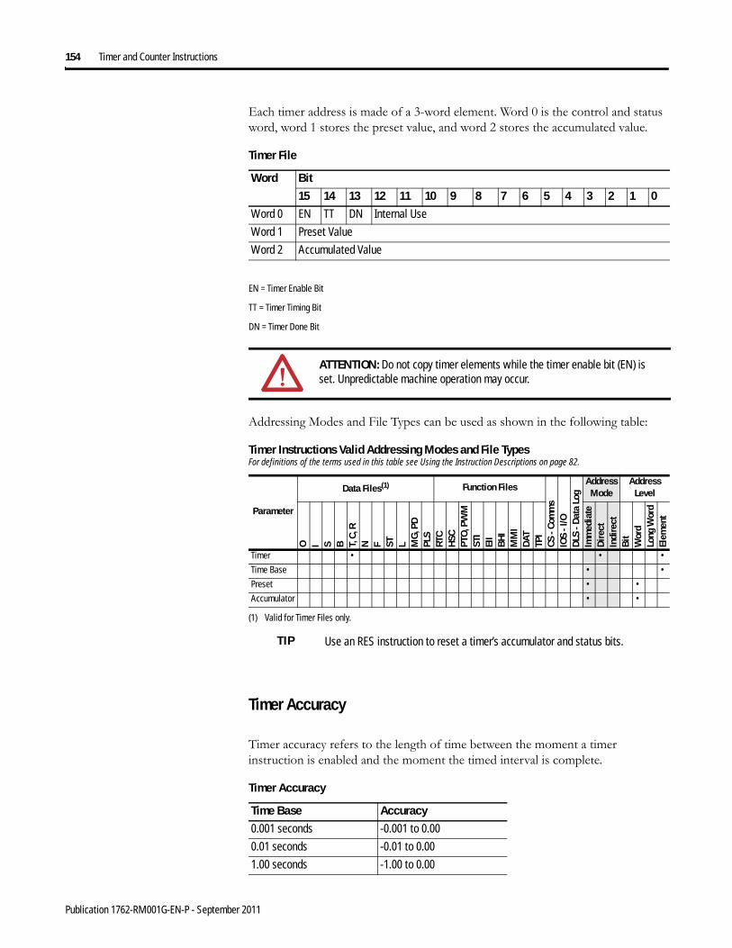
154 Timer and Counter Instructions
Each timer address is made of a 3-word element. Word 0 is the control and status word, word 1 stores the preset value, and word 2 stores the accumulated value.
EN = Timer Enable Bit
TT = Timer Timing Bit
DN = Timer Done Bit
Addressing Modes and File Types can be used as shown in the following table:
Timer Accuracy
Timer accuracy refers to the length of time between the moment a timer instruction is enabled and the moment the timed interval is complete.
Timer File
Word Bit15 14 13 12 11 10 9 8 7 6 5 4 3 2 1 0
Word 0 EN TT DN Internal Use
Word 1 Preset Value
Word 2 Accumulated Value
ATTENTION: Do not copy timer elements while the timer enable bit (EN) is set. Unpredictable machine operation may occur.
Timer Instructions Valid Addressing Modes and File TypesFor definitions of the terms used in this table see Using the Instruction Descriptions on page 82.
Parameter
Data Files(1)
(1) Valid for Timer Files only.
Function Files
CS -
Com
ms
IOS
- I/O
DLS
- D
ata
Log
Address Mode
Address Level
O I S B T, C
, RN F ST L M
G, P
DPL
SRT
CH
SCPT
O, P
WM
STI
EII
BHI
MM
IDA
TTP
I
Imm
edia
teD
irec
tIn
dire
ctB
itW
ord
Long
Wor
dEl
emen
t
Timer • • •
Time Base • •
Preset • •Accumulator • •
TIP Use an RES instruction to reset a timer’s accumulator and status bits.
Timer Accuracy
Time Base Accuracy0.001 seconds -0.001 to 0.00
0.01 seconds -0.01 to 0.00
1.00 seconds -1.00 to 0.00
Publication 1762-RM001G-EN-P - September 2011
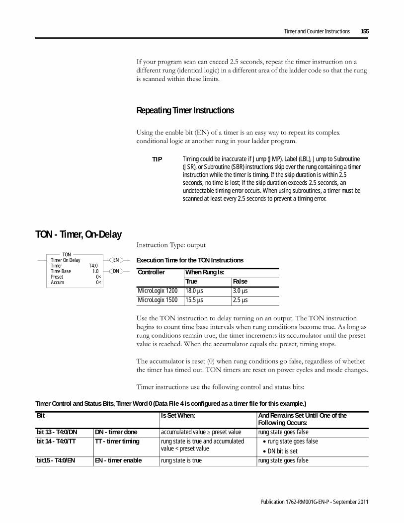
Timer and Counter Instructions 155
If your program scan can exceed 2.5 seconds, repeat the timer instruction on a different rung (identical logic) in a different area of the ladder code so that the rung is scanned within these limits.
Repeating Timer Instructions
Using the enable bit (EN) of a timer is an easy way to repeat its complex conditional logic at another rung in your ladder program.
TON - Timer, On-DelayInstruction Type: output
Use the TON instruction to delay turning on an output. The TON instruction begins to count time base intervals when rung conditions become true. As long as rung conditions remain true, the timer increments its accumulator until the preset value is reached. When the accumulator equals the preset, timing stops.
The accumulator is reset (0) when rung conditions go false, regardless of whether the timer has timed out. TON timers are reset on power cycles and mode changes.
Timer instructions use the following control and status bits:
TIP Timing could be inaccurate if Jump (JMP), Label (LBL), Jump to Subroutine (JSR), or Subroutine (SBR) instructions skip over the rung containing a timer instruction while the timer is timing. If the skip duration is within 2.5 seconds, no time is lost; if the skip duration exceeds 2.5 seconds, an undetectable timing error occurs. When using subroutines, a timer must be scanned at least every 2.5 seconds to prevent a timing error.
EN
DN
TONTimer On DelayTimer T4:0Time Base 1.0Preset 0<Accum 0<
TONExecution Time for the TON Instructions
Controller When Rung Is:True False
MicroLogix 1200 18.0 μs 3.0 μsMicroLogix 1500 15.5 μs 2.5 μs
Timer Control and Status Bits, Timer Word 0 (Data File 4 is configured as a timer file for this example.)
Bit Is Set When: And Remains Set Until One of the Following Occurs:
bit 13 - T4:0/DN DN - timer done accumulated value ≥ preset value rung state goes falsebit 14 - T4:0/TT TT - timer timing rung state is true and accumulated
value < preset value• rung state goes false
• DN bit is setbit15 - T4:0/EN EN - timer enable rung state is true rung state goes false
Publication 1762-RM001G-EN-P - September 2011
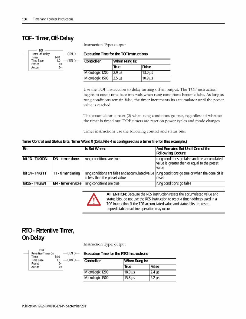
156 Timer and Counter Instructions
TOF - Timer, Off-DelayInstruction Type: output
Use the TOF instruction to delay turning off an output. The TOF instruction begins to count time base intervals when rung conditions become false. As long as rung conditions remain false, the timer increments its accumulator until the preset value is reached.
The accumulator is reset (0) when rung conditions go true, regardless of whether the timer is timed out. TOF timers are reset on power cycles and mode changes.
Timer instructions use the following control and status bits:
RTO - Retentive Timer, On-Delay
Instruction Type: output
EN
DN
TOFTimer Off DelayTimer T4:0Time Base 1.0Preset 0<Accum 0<
TOFExecution Time for the TOF Instructions
Controller When Rung Is:True False
MicroLogix 1200 2.9 μs 13.0 μsMicroLogix 1500 2.5 μs 10.9 μs
Timer Control and Status Bits, Timer Word 0 (Data File 4 is configured as a timer file for this example.)
Bit Is Set When: And Remains Set Until One of the Following Occurs:
bit 13 - T4:0/DN DN - timer done rung conditions are true rung conditions go false and the accumulated value is greater than or equal to the preset value
bit 14 - T4:0/TT TT - timer timing rung conditions are false and accumulated value is less than the preset value
rung conditions go true or when the done bit is reset
bit15 - T4:0/EN EN - timer enable rung conditions are true rung conditions go false
ATTENTION: Because the RES instruction resets the accumulated value and status bits, do not use the RES instruction to reset a timer address used in a TOF instruction. If the TOF accumulated value and status bits are reset, unpredictable machine operation may occur.
EN
DN
RTORetentive Timer OnTimer T4:0Time Base 1.0Preset 0<Accum 0<
RTOExecution Time for the RTO Instructions
Controller When Rung Is:True False
MicroLogix 1200 18.0 μs 2.4 μsMicroLogix 1500 15.8 μs 2.2 μs
Publication 1762-RM001G-EN-P - September 2011

Timer and Counter Instructions 157
Use the RTO instruction to delay turning “on” an output. The RTO begins to count time base intervals when the rung conditions become true. As long as the rung conditions remain true, the timer increments its accumulator until the preset value is reached.
The RTO retains the accumulated value when the following occur:
• rung conditions become false• you change the controller mode from run or test to program• the processor loses power• a fault occurs
When you return the controller to the RUN or TEST mode, and/or the rung conditions go true, timing continues from the retained accumulated value. RTO timers are retained through power cycles and mode changes.
Timer instructions use the following control and status bits:
To reset the accumulator of a retentive timer, use an RES instruction. See RES - Reset on page 160.
How Counters Work The figure below demonstrates how a counter works. The count value must remain in the range of -32,768 to +32,767. If the count value goes above +32,767, the counter status overflow bit (OV) is set (1). If the count goes below -32,768, the counter status underflow bit (UN) is set (1). A reset (RES) instruction is used to reset (0) the counter.
Counter Control and Status Bits, Timer Word 0 (Data File 4 is configured as a timer file for this example.)
Bit Is Set When: And Remains Set Until One of the Following Occurs:
bit 13 - T4:0/DN DN - timer done accumulated value ≥ preset value the appropriate RES instruction is enabledbit 14 - T4:0/TT TT - timer timing rung state is true and accumulated
value < preset value• rung state goes false, or
• DN bit is setbit15 - T4:0/EN EN - timer enable rung state is true rung state goes false
-32,768 +32,7670
OverflowUnderflow
Counter Accumulator Value
Count Up
Count Down
Publication 1762-RM001G-EN-P - September 2011

158 Timer and Counter Instructions
Using the CTU and CTD Instructions
Counter instructions use the following parameters:
• Counter - This is the address of the counter within the data file. All counters are 3-word data elements. Word 0 contains the Control and Status Bits, Word 1 contains the Preset, and Word 2 contains the Accumulated Value.
CU = Count Up Enable Bit
CD = Count Down Enable Bit
DN = Count Done Bit
OV = Count Overflow Bit
UN = Count Underflow Bit
• Preset - When the accumulator reaches this value, the DN bit is set. The preset data range is from -32768 to 32767.
• Accumulator - The accumulator contains the current count. The accumulator data range is from -32768 to 32767.
The accumulated value is incremented (CTU) or decremented (CTD) on each false-to-true rung transition. The accumulated value is retained when the rung condition again becomes false, and when power is cycled on the controller. The accumulated count is retained until cleared by a reset (RES) instruction that has the same address as the counter.
Addressing Modes and File Types can be used as shown in the following table:
Word Bit15 14 13 12 11 10 9 8 7 6 5 4 3 2 1 0
Word 0 CU CD DN OV UN Not UsedWord 1 Preset ValueWord 2 Accumulated Value
TIP The counter continues to count when the accumulator is greater than the CTU preset and when the accumulator is less than the CTD preset.
CTD and CTU Instructions Valid Addressing Modes and File TypesFor definitions of the terms used in this table see Using the Instruction Descriptions on page 82.
Parameter
Data Files(1)
(1) Valid for Counter Files only.
Function Files
CS -
Com
ms
IOS
- I/O
DLS
- D
ata
Log
Address Mode
Address Level
O I S B T, C
, RN F ST L M
G, P
DPL
SRT
CH
SCPT
O, P
WM
STI
EII
BHI
MM
ID
ATTP
I
Imm
edia
teD
irect
Indi
rect
Bit
Wor
dLo
ng W
ord
Elem
ent
Counter • • •
Preset • •
Accumulator • •
Publication 1762-RM001G-EN-P - September 2011

Timer and Counter Instructions 159
Using Counter File Control and Status Bits
Like the accumulated value, the counter status bits are also retentive until reset, as described below.
CTU - Count UpCTD - Count Down
Instruction Type: output
CTU Instruction Counter Control and Status Bits, Counter Word 0 (Data File 5 is configured as a timer file for this example.)
Bit Is Set When: And Remains Set Until One of the Following Occurs:
bit 12 - C5:0/OV OV - overflow indicator
the accumulated value wraps from +32,767 to -32,768 and continues to count up
a RES instruction with the same address as the CTU instruction is enabled
bit 13 - C5:0/DN DN - done indicator
accumulated value ≥ preset value • accumulated value < preset value or,
• a RES instruction with the same address as the CTU instruction is enabled
bit 15 - C5:0/CU CU - count up enable
rung state is true • rung state is false
• a RES instruction with the same address as the CTU instruction is enabled
CTD Instruction Counter Control and Status Bits, Counter Word 0 (Data File 5 is configured as a timer file for this example.)
Bit Is Set When: And Remains Set Until One of the Following Occurs:
bit 11 - C5:0/UN UN - underflow indicator
the accumulated value wraps from -32,768 to +32,767 and continues to count down
a RES instruction with the same address as the CTD instruction is enabled
bit 13 - C5:0/DN DN - done indicator
accumulated value ≥ preset value • accumulated value < preset value or,
• a RES instruction with the same address as the CTU instruction is enabled
bit 14 - C5:0/CD CD - count down enable
rung state is true • rung state is false
• a RES instruction with the same address as the CTD instruction is enabled
CU
DN
CTUCount UpCounter C5:0Preset 0<Accum 0<
CTU
CU
DN
CTUCount DownCounter C5:0Preset 0<Accum 0<
CTD
Execution Time for the CTU and CTD Instructions
Controller CTU - When Rung Is: CTD - When Rung Is:True False True False
MicroLogix 1200 9.0 μs 9.2 μs 9.0 μs 9.0 μsMicroLogix 1500 6.4 μs 8.5 μs 7.5 μs 8.5 μs
Publication 1762-RM001G-EN-P - September 2011
160 Timer and Counter Instructions
The CTU and CTD instructions are used to increment or decrement a counter at each false-to-true rung transition. When the CTU rung makes a false-to-true transition, the accumulated value is incremented by one count. The CTD instruction operates the same, except the count is decremented.
RES - ResetInstruction Type: output
The RES instruction resets timers, counters, and control elements. When the RES instruction is executed, it resets the data defined by the RES instruction.
The RES instruction has no effect when the rung state is false. The following table shows which elements are modified:
TIP If the signal is coming from a field device wired to an input on the controller, the on and off duration of the incoming signal must not be more than twice the controller scan time (assuming 50% duty cycle). This condition is needed to enable the counter to detect false-to-true transitions from the incoming device.
RESR6:0
Execution Time for the RES Instructions
Controller When Rung Is:True False
MicroLogix 1200 5.9 μs 0.0 μsMicroLogix 1500 4.8 μs 0.0 μs
RES Instruction Operation
When using a RES instruction with a:Timer Element Counter Element Control ElementThe controller resets the:
ACC value to 0
DN bit
TT bit
EN bit
The controller resets the:
ACC value to 0
OV bit
UN bit
DN bit
CU bit
CD bit
The controller resets the:
POS value to 0
EN bit
EU bit
DN bit
EM bit
ER bit
UL bit
Publication 1762-RM001G-EN-P - September 2011

Timer and Counter Instructions 161
Addressing Modes and File Types can be used as shown in the following table:
Because the RES instruction resets the accumulated value and status bits, do not use the RES instruction to reset a timer address used in a TOF instruction. If the TOF accumulated value and status bits are reset, unpredictable machine operation or injury to personnel may occur.
RES Instruction Valid Addressing Modes and File TypesFor definitions of the terms used in this table see Using the Instruction Descriptions on page 82.
Parameter
Data Files Function Files
CS -
Com
ms
IOS
- I/O
DLS
- D
ata
Log
Address Mode
Address Level
O I S B T, C
, RN F ST L M
G, P
DPL
SRT
CH
SCPT
O, P
WM
STI
EII
BHI
MM
ID
ATTP
I
Imm
edia
teD
irect
Indi
rect
Bit
Wor
dLo
ng W
ord
Elem
ent
Structure • • •
Publication 1762-RM001G-EN-P - September 2011

162 Timer and Counter Instructions
Notes:
Publication 1762-RM001G-EN-P - September 2011

Chapter 9
Compare Instructions
Use these input instructions when you want to compare values of data.
Using the Compare Instructions
Most of the compare instructions use two parameters, Source A and Source B (MEQ and LIM have an additional parameter and are described later in this chapter). Both sources cannot be immediate values. The valid data ranges for these instructions are:
-32768 to 32767 (word)
-2,147,483,648 to 2,147,483,647 (long word)
Addressing Modes and File Types can be used as shown in the following table:
Instruction Used To: Page
EQU - Equal Test whether two values are equal (=) 164
NEQ - Not Equal Test whether one value is not equal to a second value (≠)
164
LES - Less Than Test whether one value is less than a second value (<)
165
LEQ - Less Than or Equal To Test whether one value is less than or equal to a second value (≤)
165
GRT - Greater Than Test whether one value is greater than a second value (>)
165
GEQ - Greater Than or Equal To Test whether one value is greater than or equal to a second value (≥)
165
MEQ - Mask Compare for Equal Test portions of two values to see whether they are equal
166
LIM - Limit Test Test whether one value is within the range of two other values
167
EQU, NEQ, GRT, LES, GEQ and LEQ Instructions Valid Addressing Modes and File TypesFor definitions of the terms used in this table see Using the Instruction Descriptions on page 82.
Parameter
Data Files Function Files(1)
CS -
Com
ms
IOS
- I/O
DLS
- Da
ta L
og(2
) Address
Mode(3)Address
Level
O I S B T, C
, RN F(4
)
ST L MG
, PD
PLS
RTC
HSC
(5)
PTO
, PW
MST
IEI
IB
HIM
MI
DAT
TPI
Imm
edia
teD
irect
Indi
rect
Bit
Wor
dLo
ng W
ord
Elem
ent
Source A • • • • • • • • • • • • • • • • • • • • • • • • •
Source B • • • • • • • • • • • • • • • • • • • • • • • • •
163 Publication 1762-RM001G-EN-P - September 2011

164 Compare Instructions
When at least one of the operands is a Floating Data Point value:
• For EQU, GEQ, GRT, LEQ, and LES - If either Source is not a number (NAN), then rung state changes to false.
• For NEQ - If either Source is not a number (NAN), then rung state remains true.
EQU - EqualNEQ - Not Equal
Instruction Type: input
The EQU instruction is used to test whether one value is equal to a second value. The NEQ instruction is used to test whether one value is not equal to a second value.
(1) DAT files are valid for the MicroLogix 1500 only. PTO and PWM files are only for use with MicroLogix 1200 and 1500 BXB units.
(2) The Data Log Status file can only be used by the MicroLogix 1500 1764-LRP Processor.
(3) See Important note about indirect addressing.
(4) The F file is valid for MicroLogix 1200 and 1500 Series C and higher controllers only.
(5) Only use the High Speed Counter Accumulator (HSC.ACC) for Source A in GRT, LES, GEQ and LEQ instructions.
IMPORTANT You cannot use indirect addressing with: S, ST, MG, PD, RTC, HSC, PTO, PWM, STI, EII, BHI, MMI, DAT, TPI, CS, IOS, and DLS files.
EQUEqualSource A N7:0 0<Source B N7:1 0<
EQU
NEQNot EqualSource A N7:0 0<Source B N7:1 0<
NEQ
Execution Time for the EQU and NEQ Instructions
Controller Instruction Data Size When Rung Is:True False
MicroLogix 1200 EQU word 1.3 μs 1.1 μslong word 2.8 μs 1.9 μs
NEQ word 1.3 μs 1.1 μslong word 2.5 μs 2.7 μs
MicroLogix 1500 EQU word 1.2 μs 1.1 μslong word 2.6 μs 1.9 μs
NEQ word 1.2 μs 1.1 μslong word 2.3 μs 2.5 μs
EQU and NEQ Instruction Operation
Instruction Relationship of Source Values Resulting Rung StateEQU A = B true
A ≠ B falseNEQ A = B false
A ≠ B true
Publication 1762-RM001G-EN-P - September 2011

Compare Instructions 165
GRT - Greater ThanLES - Less Than
Instruction Type: input
The GRT instruction is used to test whether one value is greater than a second value. The LES instruction is used to test whether one value is less than a second value.
GEQ - Greater Than or Equal ToLEQ - Less Than or Equal To
Instruction Type: input
GRTGreater Than (A>B)Source A N7:0 0<Source B N7:1 0<
GRT
LESLess Than (A<B)Source A N7:0 0<Source B N7:1 0<
LES
Execution Time for the GRT and LES Instructions
Controller Data Size When Rung Is:True False
MicroLogix 1200 word 1.3 μs 1.1 μslong word 2.8 μs 2.7 μs
MicroLogix 1500 word 1.2 μs 1.1 μslong word 2.6 μs 2.5 μs
GRT and LES Instruction Operation
Instruction Relationship of Source Values Resulting Rung StateGRT A > B true
A ≤ B falseLES A ≥ B false
A < B true
IMPORTANT Only use the High Speed Counter Accumulator (HSC.ACC) for Source A in GRT, LES, GEQ and LEQ instructions.
GEQGrtr Than or Eql (A>=B)Source A N7:0 0<Source B N7:1 0<
GEQ
LEQLess Than or Eql (A<=B)Source A N7:0 0<Source B N7:1 0<
LEQ
Execution Time for the GEQ and LEQ Instructions
Controller Data Size When Rung Is:True False
MicroLogix 1200 word 1.3 μs 1.1 μslong word 2.8 μs 2.7 μs
MicroLogix 1500 word 1.2 μs 1.1 μslong word 2.6 μs 2.5 μs
Publication 1762-RM001G-EN-P - September 2011

166 Compare Instructions
The GEQ instruction is used to test whether one value is greater than or equal to a second value. The LEQ instruction is used to test whether one value is less than or equal to a second value.
MEQ - Mask Compare for Equal
Instruction Type: input
The MEQ instruction is used to compare whether one value (source) is equal to a second value (compare) through a mask. The source and the compare are logically ANDed with the mask. Then, these results are compared to each other. If the resulting values are equal, the rung state is true. If the resulting values are not equal, the rung state is false. For example:
The source, mask, and compare values must all be of the same data size (either word or long word). The data ranges for mask and compare are:
• -32768 to 32767 (word)• -2,147,483,648 to 2,147,483,647 (long word)
GEQ and LEQ Instruction Operation
Instruction Relationship of Source Values Resulting Rung StateGEQ A ≥ B true
A < B falseLEQ A > B false
A ≤ B true
IMPORTANT Only use the High Speed Counter Accumulator (HSC.ACC) for Source A in GRT, LES, GEQ and LEQ instructions.
MEQMasked EqualSource N7:0 0<Mask N7:1 0000h<Compare N7:2 0<
MEQExecution Time for the MEQ Instructions
Controller Data Size When Rung Is:True False
MicroLogix 1200 word 1.9 μs 1.8 μslong word 3.9 μs 3.1 μs
MicroLogix 1500 word 1.7 μs 1.7 μslong word 3.5 μs 2.9 μs
Source: Compare: 1 1 1 1 1 0 1 0 0 0 0 0 1 1 0 0 1 1 1 1 1 1 1 1 0 0 0 0 0 0 0 0Mask: Mask:1 1 0 0 1 1 1 1 1 1 0 0 0 0 1 1 1 1 0 0 1 1 1 1 1 1 0 0 0 0 1 1Intermediate Result: Intermediate Result:1 1 0 0 1 0 1 0 0 0 0 0 0 0 0 0 1 1 0 0 1 1 1 1 0 0 0 0 0 0 0 0Comparison of the Intermediate Results: not equal
Publication 1762-RM001G-EN-P - September 2011

Compare Instructions 167
The mask is displayed as a hexadecimal unsigned value from 0000 to FFFF FFFF.
Addressing Modes and File Types can be used as shown in the following table:
LIM - Limit TestInstruction Type: input
The LIM instruction is used to test for values within or outside of a specified range. The LIM instruction is evaluated based on the Low Limit, Test, and High Limit values as shown in the following table.
The Low Limit, Test, and High Limit values can be word addresses or constants, restricted to the following combinations:
MEQ Instruction Valid Addressing Modes and File TypesFor definitions of the terms used in this table see Using the Instruction Descriptions on page 82.
Parameter
Data Files Function Files(1)
(1) DAT files are valid for the MicroLogix 1500 only. PTO and PWM files are only for use with MicroLogix 1200 and 1500 BXB units.
CS -
Com
ms
IOS
- I/O
DLS
- D
ata
Log(2
)
(2) The Data Log Status file can only be used by the MicroLogix 1500 1764-LRP Processor.
Address Mode(3)
(3) See Important note about indirect addressing.
Address Level
O I S B T, C
, RN F ST L M
G, P
DPL
SRT
CH
SCPT
O, P
WM
STI
EII
BHI
MM
IDA
TTP
I
Imm
edia
teD
irec
tIn
dire
ctB
itW
ord
Long
Wor
dEl
emen
t
Source • • • • • • • • • • • • • • • • • • • • • • • •
Mask • • • • • • • • • • • • • • • • • • • • • • • • •
Compare • • • • • • • • • • • • • • • • • • • • • • • • •
IMPORTANT You cannot use indirect addressing with: S, ST, MG, PD, RTC, HSC, PTO, PWM, STI, EII, BHI, MMI, DAT, TPI, CS, IOS, and DLS files.
LIMLimit TestLow Lim N7:0 0<Test 0 0<High Lim N7:1 0<
LIMExecution Time for the LIM Instructions
Controller Data Size When Rung Is:True False
MicroLogix 1200 word 6.4 μs 6.1 μslong word 14.4 μs 13.6 μs
MicroLogix 1500 word 5.5 μs 5.3 μslong word 12.2 μs 11.7 μs
LIM Instruction Operation Based on Low Limit, Test, and High Limit Values
When: And: Rung StateLow Limit ≤ High Limit Low Limit ≤ Test ≤ High Limit true
Low Limit ≤ High Limit Test < Low Limit or Test > High Limit false
High Limit < Low Limit High Limit < Test < Low Limit false
High Limit < Low Limit Test ≥ High Limit or Test ≤ Low Limit true
Publication 1762-RM001G-EN-P - September 2011
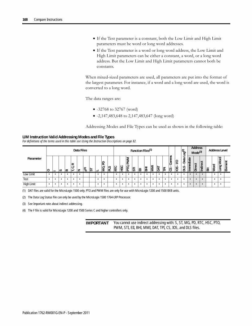
168 Compare Instructions
• If the Test parameter is a constant, both the Low Limit and High Limit parameters must be word or long word addresses.
• If the Test parameter is a word or long word address, the Low Limit and High Limit parameters can be either a constant, a word, or a long word address. But the Low Limit and High Limit parameters cannot both be constants.
When mixed-sized parameters are used, all parameters are put into the format of the largest parameter. For instance, if a word and a long word are used, the word is converted to a long word.
The data ranges are:
• -32768 to 32767 (word)• -2,147,483,648 to 2,147,483,647 (long word)
Addressing Modes and File Types can be used as shown in the following table:
LIM Instruction Valid Addressing Modes and File TypesFor definitions of the terms used in this table see Using the Instruction Descriptions on page 82.
Parameter
Data Files Function Files(1)
CS -
Com
ms
IOS
- I/O
DLS
- D
ata
Log(2
) Address Mode(3) Address Level
O I S B T, C
, R
N F(4)
ST L MG
, PD
PLS
RTC
HSC
PTO
, PW
M
STI
EII
BHI
MM
I
DAT
TPI
Imm
edia
te
Dire
ct
Indi
rect
Bit
Wor
d
Long
Wor
d
Elem
ent
Low Limit • • • • • • • • • • • • • • • • • • • • • • • • •
Test • • • • • • • • • • • • • • • • • • • • • • • • •
High Limit • • • • • • • • • • • • • • • • • • • • • • • • •
(1) DAT files are valid for the MicroLogix 1500 only. PTO and PWM files are only for use with MicroLogix 1200 and 1500 BXB units.
(2) The Data Log Status file can only be used by the MicroLogix 1500 1764-LRP Processor.
(3) See Important note about indirect addressing.
(4) The F file is valid for MicroLogix 1200 and 1500 Series C and higher controllers only.
IMPORTANT You cannot use indirect addressing with: S, ST, MG, PD, RTC, HSC, PTO, PWM, STI, EII, BHI, MMI, DAT, TPI, CS, IOS, and DLS files.
Publication 1762-RM001G-EN-P - September 2011
Chapter 10
Math Instructions
General Information
Before using math instructions, become familiar with the following topics at the beginning of this chapter:
• Using the Math Instructions• Updates to Math Status Bits• Using the Floating Point (F) Data File
Instructions
Use these output instructions to perform computations using an expression or a specific arithmetic instruction.
Using the Math Instructions
Most math instructions use three parameters, Source A, Source B, and Destination (additional parameters are described where applicable, later in this chapter). The mathematical operation is performed using both Source values. The result is stored in the Destination.
When using math instructions, observe the following:
Instruction Used To: Page
ADD - Add Add two values 174
SUB - Subtract Subtract two values 174
MUL - Multiply Multiply two values 175
DIV - Divide Divide one value by another 175
NEG - Negate Change the sign of the source value and place it in the destination
175
CLR - Clear Set all bits of a word to zero 176
ABS - Absolute Value Find the absolute value of the source value 176
SQR - Square Root Find the square root of a value 180
SCL - Scale Scale a value 177
SCP - Scale with Parameters Scale a value to a range determined by creating a linear relationship
178
169 Publication 1762-RM001G-EN-P - September 2011

170 Math Instructions
• Source and Destination can be different data sizes. Sources are evaluated at the highest precision (word or long word) of the operands. Then the result is converted to the size of the destination. If the signed value of the Source does not fit in the Destination, the overflow shall be handled as follows:– If the Math Overflow Selection Bit is clear, a saturated result is stored in
the Destination. If the Source is positive, the Destination is +32767 (word) or +2,147,483,647 (long word). If the result is negative, the Destination is -32768 (word) or -2,147,483,648 (long word).
– If the Math Overflow Selection Bit is set, the unsigned truncated value of the Source is stored in the Destination.
• Sources can be constants or an address, but both sources cannot be constants.
• Valid constants are -32768 to 32767 (word) and -2,147,483,648 to 2,147,483,647 (long word).
Addressing Modes and File Types can be used as shown in the following table:
Updates to Math Status Bits
After a math instruction is executed, the arithmetic status bits in the status file are updated. The arithmetic status bits are in word 0 in the processor status file (S2).
Math Instructions (ADD, SUB, MUL, DIV, NEG, CLR) Valid Addressing Modes and File TypesFor definitions of the terms used in this table see Using the Instruction Descriptions on page 82.
Parameter
Data Files Function Files(1)
CS -
Com
ms
IOS
- I/O
DLS
- D
ata
Log(2
) Address Mode(3) Address Level
O I S B T, C
, R
N F(4)
ST L MG
, PD
PLS
RTC
HSC
PTO
, PW
M
STI
EII
BHI
MM
I
DAT
TPI
Imm
edia
te
Dir
ect
Indi
rect
Bit
Wor
d
Long
Wor
d
Elem
ent
Source A • • • • • • • • • • • • • • • • • • • • • • • • • •
Source B • • • • • • • • • • • • • • • • • • • • • • • • • •
Destination • • • • • • • • • • • • • • • • • • •
(1) DAT files are valid for the MicroLogix 1500 only. PTO and PWM files are only for use with MicroLogix 1200 and 1500 BXB units.
(2) The Data Log Status file can only be used by the MicroLogix 1500 1764-LRP Processor for the following math instructions: ADD, SUB, MUL, DIV, NEG, and SCP.
(3) See Important note about indirect addressing.
(4) The F file is valid for MicroLogix 1200 and 1500 Series C and higher controllers only.
IMPORTANT You cannot use indirect addressing with: S, ST, MG, PD, RTC, HSC, PTO, PWM, STI, EII, BHI, MMI, DAT, TPI, CS, IOS, and DLS files.
Math Status Bits
With this Bit: The Controller:S:0/0 Carry sets if carry is generated; otherwise resetsS:0/1 Overflow sets when the result of a math instruction does not fit into the
destination, otherwise resetsS:0/2 Zero Bit sets if result is zero, otherwise resetsS:0/3 Sign Bit sets if result is negative (MSB is set), otherwise resets
Publication 1762-RM001G-EN-P - September 2011
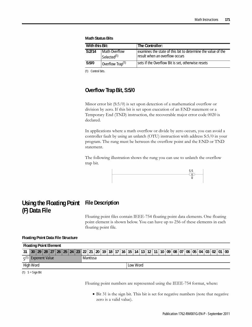
Math Instructions 171
Overflow Trap Bit, S:5/0
Minor error bit (S:5/0) is set upon detection of a mathematical overflow or division by zero. If this bit is set upon execution of an END statement or a Temporary End (TND) instruction, the recoverable major error code 0020 is declared.
In applications where a math overflow or divide by zero occurs, you can avoid a controller fault by using an unlatch (OTU) instruction with address S:5/0 in your program. The rung must be between the overflow point and the END or TND statement.
The following illustration shows the rung you can use to unlatch the overflow trap bit.
Using the Floating Point (F) Data File
File Description
Floating point files contain IEEE-754 floating point data elements. One floating point element is shown below. You can have up to 256 of these elements in each floating point file.
Floating point numbers are represented using the IEEE-754 format, where:
• Bit 31 is the sign bit. This bit is set for negative numbers (note that negative zero is a valid value).
S:2/14 Math Overflow Selected(1)
examines the state of this bit to determine the value of the result when an overflow occurs
S:5/0 Overflow Trap(1) sets if the Overflow Bit is set, otherwise resets
(1) Control bits.
Math Status Bits
With this Bit: The Controller:
US:5
0
Floating Point Data File Structure
Floating Point Element31 30 29 28 27 26 25 24 23 22 21 20 19 18 17 16 15 14 13 12 11 10 09 08 07 06 05 04 03 02 01 00
S(1) Exponent Value Mantissa
High Word Low Word
(1) S = Sign Bit
Publication 1762-RM001G-EN-P - September 2011

172 Math Instructions
• Bits 23 to 30 are the exponent.• Bits 0 to 22 are the mantissa.
The value represented by a 32-bit floating point number (not one of the exception values defined on page 172) is given by the following expression. Note the restoration of the suppressed most significant bit of the mantissa.
(-1)s x 2 e - 127 x (1 + m)
where:
″ s is the sign bit (0 or 1)″ e is the exponent (1 to 254)″ m is the mantissa (0 ≤ f < 1)
The valid range for floating point numbers is from -3.4028 x 1038 to 3.4028 x 1038.
Definitions
Overflow - occurs when the result of an operation produces an exponent that is greater than 254.
Underflow - occurs when the result of an operation produces an exponent that is less than one.
Floating Point Exception Values
Zero - represented by an exponent and a mantissa of zero. Both positive and negative zero are valid.
Denormalized - represented by an exponent of zero and a non-zero mantissa part. Since denormalized numbers have very small, insignificant values, they are treated as zero when used as source operand for most instructions. This reduces execution time. Denormalized numbers are not generated by the instructions (but are propagated by some instructions). Zero is generated on an underflow.
Infinity - represented by an exponent of 255 and a mantissa part of zero. Both positive and negative infinity are generated when operations overflow. Infinity is propagated through calculations.
NAN (not a number) - is represented by an exponent of 255 and a non-zero mantissa part. NANs are used to indicate results that are mathematically undefined such as 0/0 and adding plus infinity to minus infinity. All operations given a NAN as input must generate a NAN as output.
Publication 1762-RM001G-EN-P - September 2011

Math Instructions 173
LSB Round-to-Even Rule
Floating point operations are rounded using the round-to-even rule. If the bits of the result to the right of the least significant bit (LSB) represent a value less than one-half of the LSB, then the result remains as is. If the bits to the right of the LSB represent a value greater than one-half of the LSB, the result is rounded up by adding one LSB. If the bits to the right of the LSB represent a value of exactly one-half LSB, the result is rounded up or down so that the LSB is an even number.
Addressing Floating Point Files
The addressing format for floating point data files is shown below.
Programming Floating Point Values
The following table shows items to consider when using floating point data.
Format ExplanationFf:e F Floating Point file
f File number The valid file number range is from 8 (default) to 255.
: Element delimiter
e Element number The valid element number range is from 0 to 255.
Examples: F8:2F10:36
Floating Point File 8, Element 2Floating Point File 10, Element 36
IMPORTANT These rules do not apply to the SCP instruction. See page 179 for the rules for that instruction.
Publication 1762-RM001G-EN-P - September 2011

174 Math Instructions
ADD - AddSUB - Subtract
Instruction Type: output
Considerations When Using Floating Point DataWhen at least one of the operands is a Floating Data Point value:
• If either Source is NAN, then the result is NAN.
• All overflows result in infinity with the correct sign.
• All underflows result in plus zero.
• All denormalized Source values are treated as plus zero.
• Results are always rounded using the Round to Even rule.
• If Destination is an integer and the result is NAN or infinity, a saturated result (-32768 or +32767 for word or -2,147,836,648 or +2,147,836,647 for long word) is stored in Destination and the Math Overflow Selection Bit is ignored.
• If Destination is an integer, the rounded result is stored. If an overflow occurs after rounding, a saturated result is stored in Destination and the Math Overflow Selection Bit is ignored. The saturated results are:
– If Destination is an integer and the result is positive, overflow Destination is +32767 (word) or +2,147,483, 648 (long word).
– If Destination is an integer and the result is negative, overflow Destination is -32767 (word) or -2,147,483, 648 (long word).
Updates to Math Status Bits:
• Carry - is reset
• Overflow - Is set if the result is infinity, NAN, or if a conversion to integer overflows; otherwise it is reset.
• Zero - Is set if the lower 31 bits of the Floating Point Data result is all zero’s, otherwise it is reset.
• Sign - Is set if the most significant bit of the Destination is set (bit 15 for word, bit 31 for long word or floating point data); otherwise it is reset.
• Overflow Trap - The Math Overflow Trap Bit is only set if the Overflow bit is set. Otherwise, it remains in its last state.
ADDAddSource A N7:0 0<Source B N7:1 0<Dest N7:2 0<
ADD
SUBSubtractSource A N7:0 0<Source B N7:1 0<Dest N7:2 0<
SUB
Execution Time for the ADD and SUB Instructions
Controller Instruction Data Size When Rung Is:True False
MicroLogix 1200 ADD word 2.7 μs 0.0 μslong word 11.9 μs 0.0 μs
SUB word 3.4 μs 0.0 μslong word 12.9 μs 0.0 μs
MicroLogix 1500 ADD word 2.5 μs 0.0 μslong word 10.4 μs 0.0 μs
SUB word 2.9 μs 0.0 μslong word 11.2 μs 0.0 μs
Publication 1762-RM001G-EN-P - September 2011

Math Instructions 175
Use the ADD instruction to add one value to another value (Source A + Source B) and place the sum in the Destination.
Use the SUB instruction to subtract one value from another value (Source A - Source B) and place the result in the Destination.
MUL - MultiplyDIV - Divide
Instruction Type: output
Use the MUL instruction to multiply one value by another value (Source A x Source B) and place the result in the Destination.
Use the DIV instruction to divide one value by another value (Source A/Source B) and place the result in the Destination. If the Sources are single words and the Destination is directly addressed to S:13 (math register), then the quotient is stored in S:14 and the remainder is stored in S:13. If long words are used, then the results are rounded.
NEG - NegateInstruction Type: output
Use the NEG instruction to change the sign of the Source and place the result in the Destination.
MULMultiplySource A N7:0 0<Source B N7:1 0<Dest N7:2 0<
MUL
DIVDivideSource A N7:0 0<Source B N7:1 0<Dest N7:2 0<
DIV
Execution Time for the MUL and DIV Instructions
Controller Instruction Data Size When Rung Is:True False
MicroLogix 1200 MUL word 6.8 μs 0.0 μslong word 31.9 μs 0.0 μs
DIV word 12.2 μs 0.0 μslong word 42.8 μs 0.0 μs
MicroLogix 1500 MUL word 5.8 μs 0.0 μslong word 27.6 μs 0.1 μs
DIV word 10.3 μs 0.0 μslong word 36.7 μs 0.0 μs
NEGNegateSource N7:0 0<Dest N7:1 0<
NEG Execution Time for the NEG Instruction
Controller Data Size When Rung Is:True False
MicroLogix 1200 word 2.9 μs 0.0 μslong word 12.1 μs 0.0 μs
MicroLogix 1500 word 1.9 μs 0.0 μslong word 10.4 μs 0.0 μs
Publication 1762-RM001G-EN-P - September 2011

176 Math Instructions
CLR - ClearInstruction Type: output
Use the CLR instruction to set the Destination to a value of zero.
ABS - Absolute Value Instruction Type: output
The ABS instruction takes the absolute value of the Source and places it in the Destination. The data range for this instruction is -2,147,483,648 to 2,147,483,647 or IEEE-754 floating point value.
Source and Destination do not have to be the same data type. However, if the signed result does not fit in Destination, the following will occur.
CLRClearDest N7:0 0<
CLRExecution Time for the CLR Instruction
Controller Data Size When Rung Is:True False
MicroLogix 1200 word 1.3 μs 0.0 μslong word 6.3 μs 0.0 μs
MicroLogix 1500 word 1.2 μs 0.0 μslong word 5.5 μs 0.0 μs
Execution Time for the ABS Instruction
Controller When Rung Is:True False
MicroLogix 1200 3.8 μs 0.0 μsMicroLogix 1500 3.1 μs 0.0 μs
ABSAbsolute ValueSource N7:0 0<Dest N7:1 0<
ABS
ABS Result Does Not Fit in Destination
When Both Operands Are Integers When At Least One Operand is Floating Point Data• If the Math Overflow Selection Bit is clear, a saturated result
(32767 for word or 2,147,836,647 for long word) is stored in the Destination.
• If the Math Overflow Selection Bit is set, the unsigned truncated value of the result is stored in the Destination.
• The ABS instruction clears the sign bit. No operation is performed on the remaining bits.
• If Destination is an integer and Source is NAN or infinity, a saturated result (32767 for word or 2,147,836,647 for long word) is stored in Destination and the Math Overflow Selection Bit is ignored.
• If Destination is an integer, the rounded result is stored. If an overflow occurs after rounding, a saturated result (32767 for word or 2,147,836,647 for long word) is stored in Destination and the Math Overflow Selection Bit is ignored.
Publication 1762-RM001G-EN-P - September 2011

Math Instructions 177
The following table shows how the math status bits are updated upon execution of the ABS instruction:
Addressing Modes and File Types are shown in the following table:
SCL - ScaleInstruction Type: output
The SCL instruction causes the value at the Source address to be multiplied by the Rate (slope) value. The resulting value is added to the Offset and the rounded result is placed in the Destination.
The following equations express the linear relationship between the input value and the resulting scaled value:
Updates to Math Status Bits
When Both Operands Are Integers When At Least One Operand is Floating Point Data• Carry - Is set if input is negative, otherwise resets.
• Overflow - Is set if the signed result cannot fit in the Destination; otherwise it is reset.
• Zero - Is set if Destination is all zero’s, otherwise it is reset.
• Sign - Is set if the most significant bit of the Destination is set, otherwise it is reset.
• Overflow Trap - The Math Overflow Trap Bit is only set if the Overflow bit is set. Otherwise, it remains in its last state.
• Carry - Is reset.
• Overflow - Is set if the signed result is infinity, NAN, or cannot fit in the Destination; otherwise it is reset.
• Zero - Is set if Destination is all zero’s, otherwise it is reset.
• Sign - Is set if the most significant bit of the Destination is set, otherwise it is reset.
• Overflow Trap - The Math Overflow Trap Bit is only set if the Overflow bit is set. Otherwise, it remains in its last state.
ABS Instruction Valid Addressing Modes and File TypesFor definitions of the terms used in this table see Using the Instruction Descriptions on page 4-2.
Parameter
Data Files Function Files
CS -
Com
ms
IOS
- I/O
DLS
- Da
ta L
og
Address Mode(1)
(1) See Important note about indirect addressing.
Address Level
O I S B T, C
, RN F ST L M
G, P
DPL
SRT
CH
SCPT
O, P
WM
STI
EII
BHI
MM
ID
ATTP
I
Imm
edia
teD
irec
tIn
dire
ctB
itW
ord
Long
Wor
dFl
oatin
g Po
int
Elem
ent
Source • • • • • • • • • • • • • • • • • • • • • • • • • •
Destination • • • • • • • • • • • • • • • • • • • •
IMPORTANT You cannot use indirect addressing with: S, MG, PD, RTC, HSC, PTO, PWM, STI, EII, BHI, MMI, DAT, TPI, CS, IOS, and DLS files.
SCLScaleSource N7:0 0<Rate [/10000] N7:1 0<Offset N7:2 0<Dest N7:3 0<
SCLExecution Time for the SCL Instruction
Controller When Rung Is:True False
MicroLogix 1200 10.5 μs 0.0 μsMicroLogix 1500 8.7 μs 0.0 μs
Publication 1762-RM001G-EN-P - September 2011

178 Math Instructions
scaled value = [(rate x source)/10000] + offset, where
• rate = (scaled max. - scaled min.)/(input max. - input min.)• offset = scaled min. - (input min. x rate)
Rate and Offset can both be immediate values. The data range for rate and offset is -32768 to 32767.
Addressing Modes and File Types can be used as shown in the following table:
SCP - Scale with Parameters
Instruction Type: output
The SCP instruction produces a scaled output value that has a linear relationship between the input and scaled values. This instruction solves the following equation listed below to determine scaled output:
SCL Instruction Valid Addressing Modes and File TypesFor definitions of the terms used in this table see Using the Instruction Descriptions on page 82.
Parameter
Data Files Function Files
CS -
Com
ms
IOS
- I/O
DLS
- D
ata
Log
Address(1) Mode
(1) See Important note about indirect addressing.
Address Level
O I S B T, C
, RN F ST L M
G, P
DPL
SRT
CH
SCPT
O, P
WM
STI
EII
BHI
MM
IDA
TTP
I
Imm
edia
teDi
rect
Indi
rect
Bit
Wor
dLo
ng W
ord
Elem
ent
Source • • • • • • • •Rate • • • • • • • • •Offset • • • • • • • • •Destination • • • • • • • •
IMPORTANT You cannot use indirect addressing with: S, ST, MG, PD, RTC, HSC, PTO, PWM, STI, EII, BHI, MMI, DAT, TPI, CS, IOS, and DLS files.
IMPORTANT Do not use the High Speed Counter Accumulator (HSC.ACC) for the Destination parameter in the SCL instruction.
SCPScale w/ParametersInput N7:0 0<Input Min. N7:1 0<Input Max. N7:2 0<Scaled Min. N7:3 0<Scaled Max. N7:4 0<Output N7:5 0<
SCPExecution Time for the SCP Instruction
Controller Data Size When Rung Is:True False
MicroLogix 1200 word 31.5 μs 0.0 μslong word 52.2 μs 0.0 μs
MicroLogix 1500 word 27.0 μs 0.0 μslong word 44.7 μs 0.0 μs
Publication 1762-RM001G-EN-P - September 2011

Math Instructions 179
y = [(y1 - y0)/(x1 - x0)](x - x0) + y0
Addressing Modes and File Types can be used as shown in the following table:
Special Considerations when Using Floating Point Parameters
If any of the parameters (except Output) are NAN (not a number), Infinity, or De-normalized; then the result is -NAN.
If y1 - y0 or x1 - x0 result in an overflow, then the result is -NAN
Other Considerations
If y1 - y0 = 0, the Result becomes the Scaled Start value
If x1 - x0 = 0 and x = x0, the Result becomes the Scaled Start value
If x1 - x0 = 0 and x does not equal x0, The Result becomes a negative overflow (for integer values) or a negative NAN (for floating point values)
SCP Instruction Valid Addressing Modes and File TypesFor definitions of the terms used in this table see Using the Instruction Descriptions on page 82.
Parameter
Data Files Function Files(1)
CS -
Com
ms
IOS
- I/O
DLS
- D
ata
Log
Address Mode(2) Address Level
O I S B T, C
, R
N F ST L MG
, PD
PLS
RTC
HSC
PTO
, PW
M
STI
EII
BHI
MM
I
DAT
TPI
Imm
edia
te
Dire
ct
Indi
rect
Bit
Wor
d
Long
Wor
d
Elem
ent
Input (x) • • • • • • • • • • • • • • • • • • • • • • • •Input Min. (x0) • • • • • • • • • • • •Input Max. (x1) • • • • • • • • • • • •Scaled Min. (y0) • • • • • • • • • • • •Scaled Max. (y1) • • • • • • • • • • • •Output (y) • • • • • • • • • • • • • • • • • •
(1) DAT files are valid for the MicroLogix 1500 only. PTO and PWM files are only recommended for use with MicroLogix 1200 and 1500 BXB units.
(2) See Important note about indirect addressing.
IMPORTANT You cannot use indirect addressing with: S, ST, MG, PD, RTC, HSC, PTO, PWM, STI, EII, BHI, MMI, DAT, TPI, CS, IOS, and DLS files.
IMPORTANT Do not use the High Speed Counter Accumulator (HSC.ACC) for the Scaled Output parameter in the SCP instruction.
Publication 1762-RM001G-EN-P - September 2011

180 Math Instructions
SQR - Square RootInstruction Type: output
The SQR instruction calculates the square root of the absolute value of the source and places the rounded result in the destination.
The data ranges for the source is -32768 to 32767 (word) and -2,147,483,648 to 2,147,483,647 (long word). The Carry Math Status Bit is set if the source is negative. See Updates to Math Status Bits on page 170 for more information.
SQRSquare RootSource N7:0 0<Dest N7:1 0<
SQRExecution Time for the SQR Instruction
Controller Data Size When Rung Is:True False
MicroLogix 1200 word 26.0 μs 0.0 μslong word 30.9 μs 0.0 μs
MicroLogix 1500 word 22.3 μs 0.0 μslong word 26.0 μs 0.0 μs
SQR Instruction Valid Addressing Modes and File TypesFor definitions of the terms used in this table see Using the Instruction Descriptions on page 82.
Parameter
Data Files Function Files
CS -
Com
ms
IOS
- I/O
DLS
- D
ata
Log
Address Mode(1) Address Level
O I S B T, C
, R
N ST F L MG
, PD
PLS
RTC
HSC
PTO
, PW
M
STI
EII
BHI
MM
I
DAT
TPI
Imm
edia
te
Dir
ect
Indi
rect
Bit
Wor
d
Long
Wor
d
Elem
ent
Source • • • • • • • • • • • •
Destination • • • • • • • • • • •
(1) See Important note about indirect addressing.
IMPORTANT You cannot use indirect addressing with: S, ST, MG, PD, RTC, HSC, PTO, PWM, STI, EII, BHI, MMI, DAT, TPI, CS, IOS, and DLS files.
Publication 1762-RM001G-EN-P - September 2011

Chapter 11
Conversion Instructions
The conversion instructions multiplex and de-multiplex data and perform conversions between binary and decimal values.
Using Decode and Encode Instructions
Addressing Modes and File Types can be used as shown in the following table:
Instruction Used To: Page
DCD - Decode 4 to 1-of-16 Decodes a 4-bit value (0 to 15), turning on the corresponding bit in the 16-bit destination.
182
ENC - Encode 1-of-16 to 4 Encodes a 16-bit source to a 4-bit value. Searches the source from the lowest to the highest bit and looks for the first set bit. The corresponding bit position is written to the destination as an integer.
182
FRD - Convert From Binary Coded Decimal
Converts the BCD source value to an integer and stores it in the destination.
184
TOD - Convert to Binary Coded Decimal
Converts the integer source value to BCD format and stores it in the destination.
187
Conversion Instructions Valid Addressing Modes and File TypesFor definitions of the terms used in this table see Using the Instruction Descriptions on page 82.
Parameter
Data Files Function Files
CS -
Com
ms
IOS
- I/O
DLS
- Da
ta L
og
Address Mode(1) Address Level
O I S B T, C
, R
N F ST L MG
, PD
PLS
RTC
HSC
PTO
, PW
M
STI
EII
BHI
MM
I
DAT
TPI
Imm
edia
te
Dir
ect
Indi
rect
Bit
Wor
d
Long
Wor
d
Elem
ent
Source • • • • • • • •
Destination • • • • • • • •
(1) See Important note about indirect addressing.
IMPORTANT You cannot use indirect addressing with: S, ST, MG, PD, RTC, HSC, PTO, PWM, STI, EII, BHI, MMI, DAT, TPI, CS, IOS, and DLS files.
181 Publication 1762-RM001G-EN-P - September 2011

182 Conversion Instructions
DCD - Decode 4 to 1-of-16
Instruction Type: output
The DCD instruction uses the lower four bits of the source word to set one bit of the destination word. All other bits in the destination word are cleared. The DCD instruction converts the values as shown in the table below:
ENC - Encode 1-of-16 to 4 Instruction Type: output
DCDDecode 4 to 1 of 16Source N7:0 0000h<Dest N7:1 0000000000000000<
DCDExecution Time for the DCD Instruction
Controller When Rung Is:True False
MicroLogix 1200 1.9 μs 0.0 μsMicroLogix 1500 0.9 μs 0.0 μs
Decode 4 to 1-of-16
Source Bits Destination Bits15 to 04 03 02 01 00 15 14 13 12 11 10 09 08 07 06 05 04 03 02 01 00
x 0 0 0 0 0 0 0 0 0 0 0 0 0 0 0 0 0 0 0 1x 0 0 0 1 0 0 0 0 0 0 0 0 0 0 0 0 0 0 1 0x 0 0 1 0 0 0 0 0 0 0 0 0 0 0 0 0 0 1 0 0x 0 0 1 1 0 0 0 0 0 0 0 0 0 0 0 0 1 0 0 0x 0 1 0 0 0 0 0 0 0 0 0 0 0 0 0 1 0 0 0 0x 0 1 0 1 0 0 0 0 0 0 0 0 0 0 1 0 0 0 0 0x 0 1 1 0 0 0 0 0 0 0 0 0 0 1 0 0 0 0 0 0x 0 1 1 1 0 0 0 0 0 0 0 0 1 0 0 0 0 0 0 0x 1 0 0 0 0 0 0 0 0 0 0 1 0 0 0 0 0 0 0 0x 1 0 0 1 0 0 0 0 0 0 1 0 0 0 0 0 0 0 0 0x 1 0 1 0 0 0 0 0 0 1 0 0 0 0 0 0 0 0 0 0x 1 0 1 1 0 0 0 0 1 0 0 0 0 0 0 0 0 0 0 0x 1 1 0 0 0 0 0 1 0 0 0 0 0 0 0 0 0 0 0 0x 1 1 0 1 0 0 1 0 0 0 0 0 0 0 0 0 0 0 0 0x 1 1 1 0 0 1 0 0 0 0 0 0 0 0 0 0 0 0 0 0x 1 1 1 1 1 0 0 0 0 0 0 0 0 0 0 0 0 0 0 0
x = not used
ENCEncode 1 of 16 to 4Source N7:0 0000000000000000<Dest N7:1 0000h<
ENCExecution Time for the ENC Instruction
Controller When Rung Is:True False
MicroLogix 1200 7.2 μs 0.0 μsMicroLogix 1500 6.8 μs 0.0 μs
Publication 1762-RM001G-EN-P - September 2011
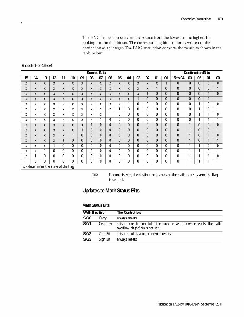
Conversion Instructions 183
The ENC instruction searches the source from the lowest to the highest bit, looking for the first bit set. The corresponding bit position is written to the destination as an integer. The ENC instruction converts the values as shown in the table below:
Updates to Math Status Bits
Encode 1-of-16 to 4
Source Bits Destination Bits15 14 13 12 11 10 09 08 07 06 05 04 03 02 01 00 15 to 04 03 02 01 00x x x x x x x x x x x x x x x 1 0 0 0 0 0x x x x x x x x x x x x x x 1 0 0 0 0 0 1x x x x x x x x x x x x x 1 0 0 0 0 0 1 0x x x x x x x x x x x x 1 0 0 0 0 0 0 1 1x x x x x x x x x x x 1 0 0 0 0 0 0 1 0 0x x x x x x x x x x 1 0 0 0 0 0 0 0 1 0 1x x x x x x x x x 1 0 0 0 0 0 0 0 0 1 1 0x x x x x x x x 1 0 0 0 0 0 0 0 0 0 1 1 1x x x x x x x 1 0 0 0 0 0 0 0 0 0 1 0 0 0x x x x x x 1 0 0 0 0 0 0 0 0 0 0 1 0 0 1x x x x x 1 0 0 0 0 0 0 0 0 0 0 0 1 0 1 0x x x x 1 0 0 0 0 0 0 0 0 0 0 0 0 1 0 1 1x x x 1 0 0 0 0 0 0 0 0 0 0 0 0 0 1 1 0 0x x 1 0 0 0 0 0 0 0 0 0 0 0 0 0 0 1 1 0 1x 1 0 0 0 0 0 0 0 0 0 0 0 0 0 0 0 1 1 1 01 0 0 0 0 0 0 0 0 0 0 0 0 0 0 0 0 1 1 1 1
x = determines the state of the flag
TIP If source is zero, the destination is zero and the math status is zero, the flag is set to 1.
Math Status Bits
With this Bit: The Controller:S:0/0 Carry always resetsS:0/1 Overflow sets if more than one bit in the source is set; otherwise resets. The math
overflow bit (S:5/0) is not set.S:0/2 Zero Bit sets if result is zero, otherwise resetsS:0/3 Sign Bit always resets
Publication 1762-RM001G-EN-P - September 2011

184 Conversion Instructions
FRD - Convert from Binary Coded Decimal (BCD)
Instruction Type: output
The FRD instruction is used to convert the Binary Coded Decimal (BCD) source value to an integer and place the result in the destination.
Addressing Modes and File Types can be used as shown in the following table:
FRD Instruction Source Operand
The source can be either a word address or the math register. The maximum BCD source values permissible are:
• 9999 if the source is a word address (allowing only a 4-digit BCD value)
• 32768 if the source is the math register (allowing a 5-digit BCD value with the lower 4 digits stored in S:13 and the high order digit in S:14).
If the source is the math register, it must be directly addressed as S:13. S:13 is the only status file element that can be used.
FRDFrom BCDSource S:0 0000h<Dest N7:0 0<
FRDExecution Time for the FRD Instructions
Controller When Rung Is:True False
MicroLogix 1200 14.1 μs 0.0 μsMicroLogix 1500 12.3 μs 0.0 μs
FRD Instruction Valid Addressing Modes and File TypesFor definitions of the terms used in this table see Using the Instruction Descriptions on page 82.
Parameter
Data Files Function Files
CS -
Com
ms
IOS
- I/O
DLS
- D
ata
Log
Address Mode(1) Address Level
O I S B T, C
, R
N F ST L MG
, PD
PLS
RTC
HSC
PTO
, PW
M
STI
EII
BHI
MM
I
DAT
TPI
Imm
edia
te
Dir
ect
Indi
rect
Bit
Wor
d
Long
Wor
d
Elem
ent
Source • • • • • • • • • (2)
Destination • • • • • • • •
(1) See Important note about indirect addressing.
(2) See FRD Instruction Source Operand on page 184.
IMPORTANT You cannot use indirect addressing with: S, ST, MG, PD, RTC, HSC, PTO, PWM, STI, EII, BHI, MMI, DAT, TPI, CS, IOS, and DLS files.
Publication 1762-RM001G-EN-P - September 2011

Conversion Instructions 185
Updates to Math Status Bits
The two rungs shown cause the controller to verify that the value I:0 remains the same for two consecutive scans before it executes the FRD. This prevents the FRD from converting a non-BCD value during an input value change.
Math Status Bits
With this Bit: The Controller:S:0/0 Carry always resetsS:0/1 Overflow sets if non-BCD value is contained at the source or the value to be
converted is greater than 32,767; otherwise resets. On overflow, the minor error flag is also set.
S:0/2 Zero Bit sets if result is zero, otherwise resetsS:0/3 Sign Bit always resets
TIP Always provide ladder logic filtering of all BCD input devices prior to performing the FRD instruction. The slightest difference in point-to-point input filter delay can cause the FRD instruction to overflow due to the conversion of a non-BCD digit.
TIP To convert numbers larger than 9999 BCD, the source must be the Math Register (S:13). You must reset the Minor Error Bit (S:5.0) to prevent an error.
]/[S:1
15
EQUEQUALSource A N7:1
0
Source B I:0.00
MOVMOVESource I:0.0
0
Dest N7:10
FRDFROM BCDSource I:0.0
0
Dest N7:20
Publication 1762-RM001G-EN-P - September 2011
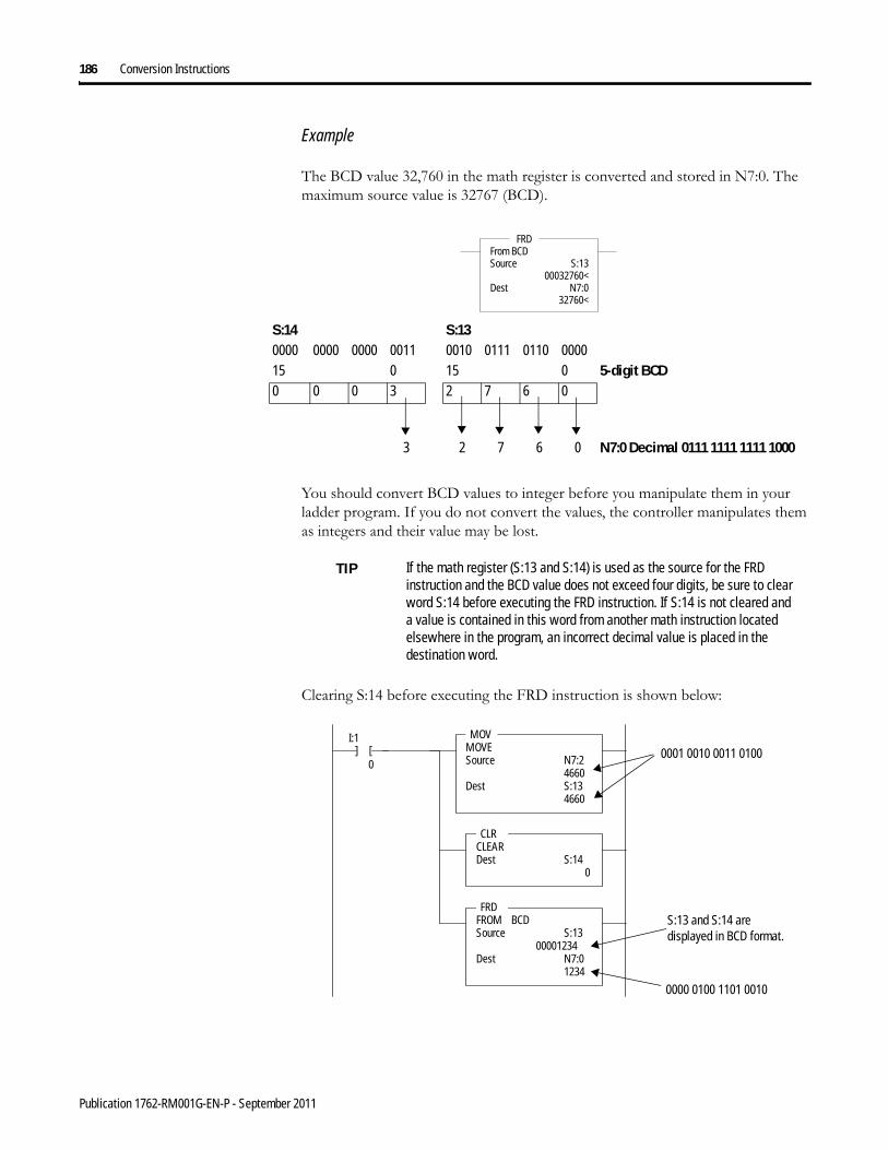
186 Conversion Instructions
Example
The BCD value 32,760 in the math register is converted and stored in N7:0. The maximum source value is 32767 (BCD).
You should convert BCD values to integer before you manipulate them in your ladder program. If you do not convert the values, the controller manipulates them as integers and their value may be lost.
Clearing S:14 before executing the FRD instruction is shown below:
FRDFrom BCDSource S:13 00032760<Dest N7:0 32760<
FRD
S:14 S:130000 0000 0000 0011 0010 0111 0110 000015 0 15 0 5-digit BCD0 0 0 3 2 7 6 0
3 2 7 6 0 N7:0 Decimal 0111 1111 1111 1000
TIP If the math register (S:13 and S:14) is used as the source for the FRD instruction and the BCD value does not exceed four digits, be sure to clear word S:14 before executing the FRD instruction. If S:14 is not cleared and a value is contained in this word from another math instruction located elsewhere in the program, an incorrect decimal value is placed in the destination word.
CLRCLEARDest S:14
0
FRDFROM BCDSource S:13
00001234Dest N7:0
1234
MOVMOVESource N7:2
4660Dest S:13
4660
] [I:1
00001 0010 0011 0100
0000 0100 1101 0010
S:13 and S:14 are displayed in BCD format.
Publication 1762-RM001G-EN-P - September 2011

Conversion Instructions 187
When the input condition I:0/1 is set (1), a BCD value (transferred from a 4-digit thumbwheel switch for example) is moved from word N7:2 into the math register. Status word S:14 is then cleared to make certain that unwanted data is not present when the FRD instruction is executed.
TOD - Convert to Binary Coded Decimal (BCD)
Instruction Type: output
The TOD instruction is used to convert the integer source value to BCD and place the result in the destination.
Addressing Modes and File Types can be used as shown in the following table:
TOD Instruction Destination Operand
The destination can be either a word address or math register.
The maximum values permissible once converted to BCD are:
• 9999 if the destination is a word address (allowing only a 4-digit BCD value)• 32768 if the destination is the math register (allowing a 5-digit BCD value
with the lower 4 digits stored in S:13 and the high order digit in S:14).
TODTo BCDSource N7:0 0<Dest N7:1 0000h<
TODExecution Time for the TOD Instructions
Controller When Rung Is:True False
MicroLogix 1200 17.2 μs 0.0 μsMicroLogix 1500 14.3 μs 0.0 μs
TOD Instruction Valid Addressing Modes and File TypesFor definitions of the terms used in this table see Using the Instruction Descriptions on page 82.
Parameter
Data Files Function Files
CS0
- Com
ms
IOS
- I/O
DLS
- D
ata
Log
Address
Mode(1) Address Level
O I S B T, C
, R
N F L MG
, PD
PLS
RTC
HSC
PTO
, PW
M
STI
EII
BHI
MM
I
DAT
TPI
Imm
edia
te
Dire
ct
Indi
rect
Bit
Wor
d
Long
Wor
d
Elem
ent
Source • • • • • • • •
Destination • • • • • • • • • (2)
(1) See Important note about indirect addressing.
(2) See TOD Instruction Destination Operand below.
IMPORTANT You cannot use indirect addressing with: S, ST, MG, PD, RTC, HSC, PTO, PWM, STI, EII, BHI, MMI, DAT, TPI, CS, IOS, and DLS files.
Publication 1762-RM001G-EN-P - September 2011
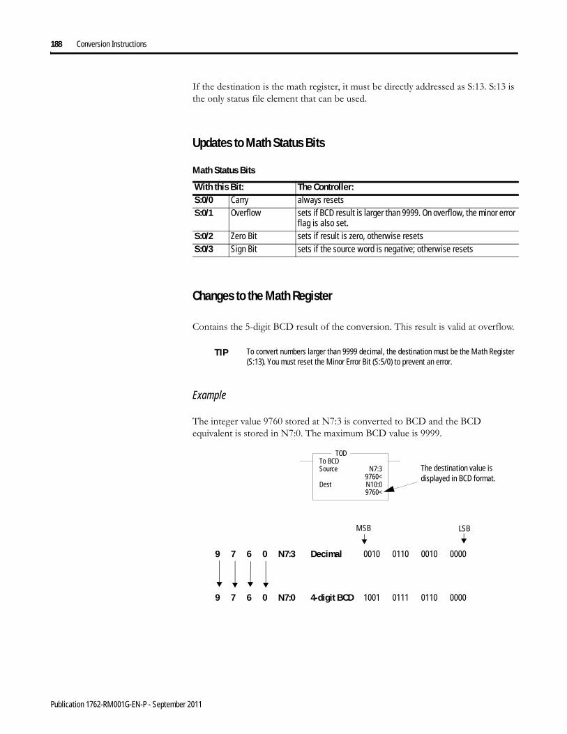
188 Conversion Instructions
If the destination is the math register, it must be directly addressed as S:13. S:13 is the only status file element that can be used.
Updates to Math Status Bits
Changes to the Math Register
Contains the 5-digit BCD result of the conversion. This result is valid at overflow.
Example
The integer value 9760 stored at N7:3 is converted to BCD and the BCD equivalent is stored in N7:0. The maximum BCD value is 9999.
Math Status Bits
With this Bit: The Controller:S:0/0 Carry always resetsS:0/1 Overflow sets if BCD result is larger than 9999. On overflow, the minor error
flag is also set.S:0/2 Zero Bit sets if result is zero, otherwise resetsS:0/3 Sign Bit sets if the source word is negative; otherwise resets
TIP To convert numbers larger than 9999 decimal, the destination must be the Math Register (S:13). You must reset the Minor Error Bit (S:5/0) to prevent an error.
TODTo BCDSource N7:3 9760<Dest N10:0 9760<
TOD
9 7 6 0 N7:3 Decimal 0010 0110 0010 0000
9 7 6 0 N7:0 4-digit BCD 1001 0111 0110 0000
MSB LSB
The destination value is displayed in BCD format.
Publication 1762-RM001G-EN-P - September 2011

Conversion Instructions 189
GCD - Gray Code Instruction Type: output
The GCD instruction converts Gray code data (Source) to an integer value (Destination). If the Gray code input is negative (high bit set), the Destination is set to 32767 and the overflow flag is set.
Addressing Modes and File Types are shown in the following table:
Updates to Math Status Bits
Execution Time for the GCD Instructions
Controller When Rung Is:True False
MicroLogix 1200 9.5 μs 0.0 μsMicroLogix 1500 8.2 μs 0.0 μs
GCDGray CodeSource I1:2.0 225<Dest N7:1 190<
GCD
GCD Instruction Valid Addressing Modes and File TypesFor definitions of the terms used in this table see Using the Instruction Descriptions on page 4-2.
Parameter
Data Files Function Files
CS -
Com
ms
IOS
- I/O
DLS
- D
ata
Log
Address Mode
Address Level
O I S B T, C
, R
N F ST L MG
, PD
PLS
RTC
HSC
PTO
, PW
M
STI
EII
BHI
MM
I
DAT
TPI
Imm
edia
te
Dir
ect
Indi
rect
Bit
Wor
d
Long
Wor
d
Elem
ent
Source • • • • • • • •
Destination • • • • • • • •
Math Status Bits
With this Bit: The Controller:S:0/0 Carry always reset
S:0/1 Overflow set if the Gray code input is negative, otherwise is reset
S:0/2 Zero Bit set if the destination is zero, otherwise reset
S:0/3 Sign Bit always reset
S:5/0 Overflow Trap set if the Overflow Bit is set, otherwise reset
Publication 1762-RM001G-EN-P - September 2011

190 Conversion Instructions
Notes:
Publication 1762-RM001G-EN-P - September 2011

Chapter 12
Logical Instructions
The logical instructions perform bit-wise logical operations on individual words.
Using Logical Instructions
When using logical instructions, observe the following:
• Source and Destination must be of the same data size (i.e. all words or all long words).
• Source A and Source B can be a constant or an address, but both cannot be constants.
• Valid constants are -32768 to 32767 (word) and -2,147,483,648 to 2,147,483,647 (long word).
Addressing Modes and File Types can be used as shown in the following table:
Instruction Used To: Page
AND - Bit-Wise AND Perform an AND operation 192
OR - Logical OR Perform an inclusive OR operation 193
XOR - Exclusive OR Perform an Exclusive Or operation 193
NOT - Logical NOT Perform a NOT operation 194
IMPORTANT Do not use the High Speed Counter Accumulator (HSC.ACC) for the Destination parameter in the AND, OR, and XOR instructions.
Logical Instructions Valid Addressing Modes and File TypesFor definitions of the terms used in this table see Using the Instruction Descriptions on page 82.
Parameter
Data Files Function Files(1)
CS -
Com
ms
IOS
- I/O
DLS
- Dat
a Lo
g(2)
Address Mode(3) Address Level
O I S B T, C
, R
N F ST L MG
, PD
PLS
RTC
HSC
PTO
, PW
M
STI
EII
BHI
MM
I
DAT
TPI
Imm
edia
te
Dir
ect
Indi
rect
Bit
Wor
d
Long
Wor
d
Elem
ent
Source A • • • • • • • • • • • • • • • • • • • • • • • • •
Source B(4) • • • • • • • • • • • • • • • • • • • • • • • • •
Destination • • • • • • • • • • • • • • • • •
(1) DAT files are valid for the MicroLogix 1500 only. PTO and PWM files are valid for MicroLogix 1200 and 1500 BXB units.
(2) The Data Log Status file can only be used by the MicroLogix 1500 1764-LRP Processor.
(3) See Important note about indirect addressing.
(4) Source B does not apply to the NOT instruction. The NOT instruction only has one source value.
191 Publication 1762-RM001G-EN-P - September 2011

192 Logical Instructions
Updates to Math Status Bits
After a logical instruction is executed, the arithmetic status bits in the status file are updated. The arithmetic status bits are in word 0 bits 0-3 in the processor status file (S2).
AND - Bit-Wise ANDInstruction Type: output
The AND instruction performs a bit-wise logical AND of two sources and places the result in the destination.
For more information, see Using Logical Instructions on page 191 and Updates to Math Status Bits on page 192.
IMPORTANT You cannot use indirect addressing with: S, ST, MG, PD, RTC, HSC, PTO, PWM, STI, EII, BHI, MMI, DAT, TPI, CS, IOS, and DLS files.
Math Status Bits
With this Bit: The Controller:S:0/0 Carry always resetsS:0/1 Overflow always resetsS:0/2 Zero Bit sets if result is zero, otherwise resetsS:0/3 Sign Bit sets if result is negative (MSB is set), otherwise resets
ANDBitwise ANDSource A N7:0 0000h<Source B N7:1 0000h<Dest N7:2 0000h<
ANDExecution Time for the AND Instruction
Controller Data Size When Rung Is:True False
MicroLogix 1200 word 2.2 μs 0.0 μslong word 9.2 μs 0.0 μs
MicroLogix 1500 word 2.0 μs 0.0 μslong word 7.9 μs 0.0 μs
Truth Table for the AND Instruction
Destination = A AND BSource: A 1 1 1 1 1 0 1 0 0 0 0 0 1 1 0 0Source: B1 1 0 0 1 1 1 1 1 1 0 0 0 0 1 1Destination:1 1 0 0 1 0 1 0 0 0 0 0 0 0 0 0
IMPORTANT Do not use the High Speed Counter Accumulator (HSC.ACC) for the Destination parameter in the AND, OR, and XOR instructions.
Publication 1762-RM001G-EN-P - September 2011

Logical Instructions 193
OR - Logical ORInstruction Type: output
The OR instruction performs a logical OR of two sources and places the result in the destination.
XOR - Exclusive ORInstruction Type: output
The XOR instruction performs a logical exclusive OR of two sources and places the result in the destination.
ORBitwise Inclusive ORSource A N7:0 0000h<Source B N7:1 0000h<Dest N7:2 0000h<
ORExecution Time for the OR Instruction
Controller Data Size When Rung Is:True False
MicroLogix 1200 word 2.2 μs 0.0 μslong word 9.2 μs 0.0 μs
MicroLogix 1500 word 2.0 μs 0.0 μslong word 7.9 μs 0.0 μs
Truth Table for the OR Instruction
Destination = A OR BSource: A 1 1 1 1 1 0 1 0 0 0 0 0 1 1 0 0Source: B1 1 0 0 1 1 1 1 1 1 0 0 0 0 1 1Destination:1 1 1 1 1 1 1 1 1 1 0 0 1 1 1 1
IMPORTANT Do not use the High Speed Counter Accumulator (HSC.ACC) for the Destination parameter in the AND, OR, and XOR instructions.
XORBitwise Exclusive ORSource A N7:0 0000h<Source B N7:1 0000h<Dest N7:2 0000h<
XORExecution Time for the XOR Instruction
Controller Data Size When Rung Is:True False
MicroLogix 1200 word 3.0 μs 0.0 μslong word 9.9 μs 0.0 μs
MicroLogix 1500 word 2.3 μs 0.0 μslong word 8.9 μs 0.0 μs
Truth Table for the XOR Instruction
Destination = A XOR BSource: A 1 1 1 1 1 0 1 0 0 0 0 0 1 1 0 0
Publication 1762-RM001G-EN-P - September 2011

194 Logical Instructions
For more information, see Using Logical Instructions on page 191 and Updates to Math Status Bits on page 192.
NOT - Logical NOTInstruction Type: output
The NOT instruction is used to invert the source bit-by-bit (one’s complement) and then place the result in the destination.
For more information, see Using Logical Instructions on page 191 and Updates to Math Status Bits on page 192.
Source: B1 1 0 0 1 1 1 1 1 1 0 0 0 0 1 1Destination:0 0 1 1 0 1 0 1 1 1 0 0 1 1 1 1
IMPORTANT Do not use the High Speed Counter Accumulator (HSC.ACC) for the Destination parameter in the AND, OR, and XOR instructions.
Truth Table for the XOR Instruction
NOTNOTSource N7:0 0<Dest N7:1 0<
NOTExecution Time for the NOT Instruction
Controller Data Size When Rung Is:True False
MicroLogix 1200 word 2.4 μs 0.0 μslong word 9.2 μs 0.0 μs
MicroLogix 1500 word 2.4 μs 0.0 μslong word 8.1 μs 0.0 μs
Truth Table for the NOT Instruction
Destination = A NOT BSource: 1 1 1 1 1 0 1 0 0 0 0 0 1 1 0 0Destination:0 0 0 0 0 1 0 1 1 1 1 1 0 0 1 1
Publication 1762-RM001G-EN-P - September 2011

Chapter 13
Move Instructions
The move instructions modify and move words.
MOV - MoveInstruction Type: output
The MOV instruction is used to move data from the source to the destination. As long as the rung remains true, the instruction moves the data each scan.
Using the MOV Instruction
When using the MOV instruction, observe the following:
• Source and Destination can be different data sizes. The source is converted to the destination size when the instruction executes. If the signed value of the Source does not fit in the Destination, the overflow is handled as follows:– If the Math Overflow Selection Bit is clear, a saturated result is stored in
the Destination. If the Source is positive, the Destination is 32767 (word). If the result is negative, the Destination is -32768.
– If the Math Overflow Selection Bit is set, the unsigned truncated value of the Source is stored in the Destination.
• Source can be a constant or an address.• Valid constants are -32768 to 32767 (word) and -2,147,483,648 to
2,147,483,647 (long word).
Instruction Used to: Page
MOV - Move Move the source value to the destination. 195
MVM - Masked Move Move data from a source location to a selected portion of the destination.
197
MOVMoveSource N7:0 0<Dest N7:1 0<
MOVExecution Time for the MOV Instruction
Controller Data Size When Rung Is:True False
MicroLogix 1200 word 2.4 μs 0.0 μslong word 8.3 μs 0.0 μs
MicroLogix 1500 word 2.3 μs 0.0 μslong word 6.8 μs 0.0 μs
195 Publication 1762-RM001G-EN-P - September 2011

196 Move Instructions
Addressing Modes and File Types can be used as shown in the following table:
Updates to Math Status Bits
After a MOV instruction is executed, the arithmetic status bits in the status file are updated. The arithmetic status bits are in word 0, bits 0 to 3 in the processor status file (S2).
MOV Instruction Valid Addressing Modes and File TypesFor definitions of the terms used in this table see Using the Instruction Descriptions on page 82.
Parameter
Data Files(1) Function Files(2)
CS -
Com
ms
IOS
- I/O
DLS
- D
ata
Log(3
) Address Mode(4) Address Level
O I S B T, C
, R
N F(5)
ST L MG
, PD
PLS
RTC
HSC
PTO
, PW
M
STI
EII
BHI
MM
I
DAT
TPI
Imm
edia
te
Dir
ect
Indi
rect
Bit
Wor
d
Long
Wor
d
Elem
ent
Source • • • • • • • • • • • • • • • • • • • • • • • • • • •
Destination • • • • • • • • • • (6) (6) (6) (6) • • • •
(1) The ST file is not valid for MicroLogix 1500 1764-LSP Series A processors.
(2) DAT files are valid for the MicroLogix 1500 only. PTO and PWM files are valid for MicroLogix 1200 and 1500 BXB units.
(3) The Data Log Status file can only be used by the MicroLogix 1500 1764-LRP Processor.
(4) See Important note about indirect addressing.
(5) The F file is valid for MicroLogix 1200 and 1500 Series C and higher controllers only.
(6) Some elements can be written to. Consult the function file for details.
IMPORTANT You cannot use indirect addressing with: S, ST, MG, PD, RTC, HSC, PTO, PWM, STI, EII, BHI, MMI, DAT, TPI, CS, IOS, and DLS files.
Math Status Bits
With this Bit: The Controller:S:0/0 Carry always resetsS:0/1 Overflow sets when an overflow, infinity, or NAN (not a number)
condition is detected, otherwise resetsS:0/2 Zero Bit sets if result is zero, otherwise resetsS:0/3 Sign Bit sets if result is negative (MSB is set), otherwise resetsS:5/0 Math Overflow Trap
Bit(1)
(1) Control bit.
sets Math Overflow Trap minor error if the Overflow bit is set, otherwise it remains in last state
TIP If you want to move one word of data without affecting the math flags, use a copy (COP) instruction with a length of 1 word instead of the MOV instruction.
Publication 1762-RM001G-EN-P - September 2011

Move Instructions 197
MVM - Masked MoveInstruction Type: output
The MVM instruction is used to move data from the source to the destination, allowing portions of the destination to be masked. The mask bit functions as follows:
Mask data by setting bits in the mask to zero; pass data by setting bits in the mask to one. The mask can be a constant, or you can vary the mask by assigning a direct address. Bits in the Destination that correspond to zeros in the Mask are not altered.
Using the MVM Instruction
When using the MVM instruction, observe the following:
• Source, Mask, and Destination must be of the same data size (i.e. all words or all long words).
To mask data, set the mask bit to zero; to pass data, set the mask bit to one. The mask can be a constant value, or you can vary the mask by assigning a direct address.
MVMMasked MoveSource N7:0 0<Mask N7:1 0000h<Dest N7:2 0<
MVMExecution Time for the MVM Instruction
Controller Data Size When Rung Is:True False
MicroLogix 1200 word 7.8 μs 0.0 μslong word 11.8 μs 0.0 μs
MicroLogix 1500 word 7.2 μs 0.0 μslong word 10.0 μs 0.0 μs
Mask Function for MVM Instruction
Source Bit Mask Bit Destination Bit1 0 last state
0 0 last state
1 1 1
0 1 0
TIP Bits in the destination that correspond to zeros in the mask are not altered as shown in the shaded areas in the following table.
Publication 1762-RM001G-EN-P - September 2011

198 Move Instructions
• Valid constants for the mask are -32768 to 32767 (word) and -2,147,483,648 to 2,147,483,647 (long word). The mask is displayed as a hexadecimal unsigned value from 0000 0000 to FFFF FFFF.
Addressing Modes and File Types can be used as shown in the following table:
Updates to Math Status Bits
After a MVM instruction is executed, the arithmetic status bits in the status file are updated. The arithmetic status bits are in word 0 bits 0-3 in the processor status file (S2).
Mask Example (Word Addressing Level)
Word Value in Hexadecimal
Value in Binary15 14 13 12 11 10 9 8 7 6 5 4 3 2 1 0
Value in Destination Before Move
FFFF 1 1 1 1 1 1 1 1 1 1 1 1 1 1 1 1
Source Value 5555 0 1 0 1 0 1 0 1 0 1 0 1 0 1 0 1Mask F0F0 1 1 1 1 0 0 0 0 1 1 1 1 0 0 0 0Value in Destination After Move
5F5F 0 1 0 1 1 1 1 1 0 1 0 1 1 1 1 1
MVM Instruction Valid Addressing Modes and File TypesFor definitions of the terms used in this table see Using the Instruction Descriptions on page 82.
Parameter
Data Files(1) Function Files
CS -
Com
ms
IOS
- I/O
DLS
- D
ata
Log
Address
Mode(2) Address Level
O I S B T, C
, R
N F ST L(3)
MG
, PD
PLS
RTC
HSC
PTO
, PW
M
STI
EII
BHI
MM
I
DAT
TPI
Imm
edia
te
Dire
ct
Indi
rect
Bit
Wor
d
Long
Wor
d
Elem
ent
Source • • • • • • • • • • •
Mask • • • • • • • • • • • •
Destination • • • • • • • • • • •
(1) The ST file is not valid for MicroLogix 1500 1764-LSP Series A processors.
(2) See Important note about indirect addressing.
(3) In earlier firmware versions, when the MVM instruction was configured to execute with a Long Word Source value set to zero, the processor could potentially lose communications or hard fault. This was corrected in MicroLogix 1200 FRN 7 and MicroLogix 1500 FRN 8 firmware.
IMPORTANT You cannot use indirect addressing with: S, ST, MG, PD, RTC, HSC, PTO, PWM, STI, EII, BHI, MMI, DAT, TPI, CS, IOS, and DLS files.
Math Status Bits
With this Bit: The Controller:S:0/0 Carry always resetsS:0/1 Overflow always resetsS:0/2 Zero Bit sets if destination is zero, otherwise resetsS:0/3 Sign Bit sets if the MSB of the destination is set, otherwise resets
Publication 1762-RM001G-EN-P - September 2011

Chapter 14
File Instructions
The file instructions perform operations on file data.
CPW - Copy Word Instruction Type: output
The CPW instruction copies words of data, in ascending order, from one location (Source) to another (Destination). Although similar to the File Copy (COP) instruction, the CPW instruction allows different source and destination parameters. Examples include:
• integer to long word• long word to floating point• long word to integer• integer to PTO function file
Instruction Used To: Page
CPW - Copy Word Copy words of data from one location to another 199
COP - Copy File Copy a range of data from one file location to another
200
FLL - Fill File Load a file with a program constant or a value from an element address
201
BSL - Bit Shift Left Load and unload data into a bit array one bit at a time
203
BSR - Bit Shift Right 204
FFL - First In, First Out (FIFO) Load Load words into a file and unload them in the same order (first in, first out)
206
FFU - First In, First Out (FIFO) Unload
208
LFL - Last In, First Out (LIFO) Load Load words into a file and unload them in reverse order (last in, first out)
210
LFU - Last In, First Out (LIFO) Unload
212
SWP - Swap(MicroLogix 1200 and 1500 Series B and higher controllers only)
Swap low byte with high byte in a specified number of words
214
Execution Time for the CPW Instruction
Controller When Rung Is:True False
MicroLogix 1200 Series C and higher only 18.3 μs + 0.8 μs/word 0.0 μsMicroLogix 1500 Series C and higher only 15.8 μs + 0.7 μs/word 0.0 μs
CPWCopy WordSource #HSC:0.2Dest #N7:0Length 1
CPW
199 Publication 1762-RM001G-EN-P - September 2011
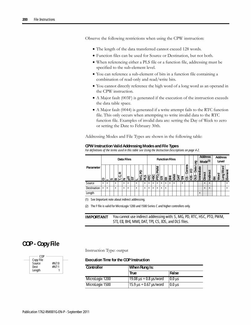
200 File Instructions
Observe the following restrictions when using the CPW instruction:
• The length of the data transferred cannot exceed 128 words.• Function files can be used for Source or Destination, but not both.• When referencing either a PLS file or a function file, addressing must be
specified to the sub-element level.• You can reference a sub-element of bits in a function file containing a
combination of read-only and read/write bits.• You cannot directly reference the high word of a long word as an operand in
the CPW instruction.• A Major fault (003F) is generated if the execution of the instruction exceeds
the data table space.• A Major fault (0044) is generated if a write attempt fails to the RTC function
file. This only occurs when attempting to write invalid data to the RTC function file. Examples of invalid data are: setting the Day of Week to zero or setting the Date to February 30th.
Addressing Modes and File Types are shown in the following table:
COP - Copy FileInstruction Type: output
CPW Instruction Valid Addressing Modes and File TypesFor definitions of the terms used in this table see Using the Instruction Descriptions on page 4-2.
Parameter
Data Files Function Files
CS -
Com
ms
IOS
- I/O
DLS
- D
ata
Log
Address Mode(1)
(1) See Important note about indirect addressing.
Address Level
O I S B T, C
, RN F(2
)
(2) The F file is valid for MicroLogix 1200 and 1500 Series C and higher controllers only.
ST L MG
, PD
PLS
RTC
HSC
PTO
, PW
MST
IEI
IBH
IM
MI
DAT
TPI
Imm
edia
teD
irec
tIn
dire
ctB
itW
ord
Long
Wor
dEl
emen
t
Source • • • • • • • • • • • • • • • • • •
Destination • • • • • • • • • • • • • • •
Length •
IMPORTANT You cannot use indirect addressing with: S, MG, PD, RTC, HSC, PTO, PWM, STI, EII, BHI, MMI, DAT, TPI, CS, IOS, and DLS files.
COPCopy FileSource #N7:0Dest #N7:1Length 1
COPExecution Time for the COP Instruction
Controller When Rung Is:True False
MicroLogix 1200 19.08 μs + 0.8 µs/word 0.0 μsMicroLogix 1500 15.9 μs + 0.67 µs/word 0.0 μs
Publication 1762-RM001G-EN-P - September 2011

File Instructions 201
The COP instruction copies blocks of data from one location into another.
The source and destination file types must be the same except bit (B) and integer (N); they can be interchanged. It is the address that determines the maximum length of the block to be copied, as shown in the following table:
FLL - Fill FileInstruction Type: output
The FLL instruction loads elements of a file with either a constant or an address data value for a given length. The following figure shows how file instruction data is manipulated. The instruction fills the words of a file with a source value. It uses no status bits. If you need an enable bit, program a parallel output that uses a storage address.
COP Instruction Valid Addressing Modes and File TypesFor definitions of the terms used in this table see Using the Instruction Descriptions on page 82.
Parameter
Data Files(1) Function Files
CS -
Com
ms
IOS
- I/O
DLS
- D
ata
Log
Address Mode(2) Address Level
O I S B T, C
, R
N F ST L MG
, PD
PLS
RTC
HSC
PTO
, PW
M
STI
EII
BHI
MM
I
DAT
TPI
Imm
edia
te
Dir
ect
Indi
rect
Bit
Wor
d
Long
Wor
d
Elem
ent
Source • • • • • • • • • • •
Destination • • • • • • • • • • •
Length •
(1) The ST file is not valid for MicroLogix 1500 1764-LSP Series A processors.
(2) See Important note about indirect addressing.
IMPORTANT You cannot use indirect addressing with: S, MG, PD, RTC, HSC, PTO, PWM, STI, EII, BHI, MMI, DAT, TPI, CS, IOS, and DLS files.
Maximum Lengths for the COP Instruction
Source/Destination Data Type Range of Length Operand1 word elements (ie. word) 1 to 1282 word elements (ie. long word) 1 to 643 word elements (ie. counter) 1 to 4242 word elements (ie. string) 1 to 3
FLLFill FileSource N7:0Dest #N7:1Length 1
FLLExecution Time for the FLL Instruction
Controller Data Size When Rung Is:True False
MicroLogix 1200 word 14 + 0.6 μs/word 0.0 μslong word 15 + 1.2 μs/long word 0.0 μs
MicroLogix 1500 word 12.1 + 0.43 μs/word 0.0 μslong word 12.3 + 0.8 μs/long word 0.0 μs
Publication 1762-RM001G-EN-P - September 2011

202 File Instructions
This instruction uses the following operands:
• Source - The source operand is the address of the value or constant used to fill the destination. The data range for the source is from -32768 to 32767 (word) or -2,147,483,648 to 2,147,483,647 (long word), or any IEEE-754 32-bit value.
• Destination - The starting destination address where the data is written.• Length - The length operand contains the number of elements. The length
can range from 1 to 128 (word), 1 to 64 (long word), or 1 to 42 (3 word element such as counter).
Addressing Modes and File Types can be used as shown in the following table:
TIP A constant cannot be used as the source in a timer (T), counter (C), or control (R) file.
TIP The source and destination operands must be of the same file type, unless they are bit (B) and integer (N).
Destination
Source
Word to File
FLL Instruction Valid Addressing Modes and File TypesFor definitions of the terms used in this table see Using the Instruction Descriptions on page 82.
Parameter
Data Files Function Files
CS -
Com
ms
IOS
- I/O
DLS
- D
ata
Log
Address Mode(1) Address Level
O I S B T, C
, R
N F(2)
ST L MG
, PD
PLS
RTC
HSC
PTO
, PW
M
STI
EII
BHI
MM
I
DAT
TPI
Imm
edia
te
Dire
ct
Indi
rect
Bit
Wor
d
Long
Wor
d
Elem
ent
Source • • • • • • • • • • • • •
Destination • • • • • • • • • •
Length •
(1) See Important note about indirect addressing.
(2) The F file is valid for MicroLogix 1200 and 1500 Series C and higher controllers only.
IMPORTANT You cannot use indirect addressing with: S, ST, MG, PD, RTC, HSC, PTO, PWM, STI, EII, BHI, MMI, DATI, TPI, CS, IOS, and DLS files.
Publication 1762-RM001G-EN-P - September 2011

File Instructions 203
BSL - Bit Shift LeftInstruction Type: output
The BSL instruction loads data into a bit array on a false-to-true rung transition, one bit at a time. The data is shifted left through the array, then unloaded, one bit at a time. The following figure shows the operation of the BSL instruction.
If you wish to shift more than one bit per scan, you must create a loop in your application using the JMP, LBL, and CTU instructions.
This instruction uses the following operands:
• File - The file operand is the address of the bit array that is to be manipulated.
• Control - The control operand is the address of the BSL’s control element. The control element consists of 3 words:
• Bit Address - The source is the address of the bit to be transferred into the bit array at the first (lowest) bit position.
• Length - The length operand contains the length of the bit array in bits. The valid data range for length is from 0 to 2048.
EN
DN
BSLBit Shift LeftFile #B3:1Control R6:0Bit Address B32:0/0Length 1<
BSLExecution Time for the BSL Instruction
Controller When Rung Is:True False
MicroLogix 1200 32 μs + 1.3 μs/word 1.3 μsMicroLogix 1500 26.1 μs + 1.06 μs/word 1.4 μs
15 14 13 12 11 10 9 8 7 6 5 4 3 2 1 0Word 0 EN(1)
(1) EN - Enable Bit is set on false-to-true transition of the rung and indicates the instruction is enabled.
-- DN(2)
(2) DN - Done Bit, when set, indicates that the bit array has shifted one position.
-- ER(3)
(3) ER - Error Bit, when set, indicates that the instruction detected an error such as entering a negative number for the length or source operand.
UL(4)
(4) UL - Unload Bit is the instruction’s output. Avoid using the UL (unload) bit when the ER (error) bit is set.
not used
Word 1 Size of bit array (number of bits).
Word 2 not used
31 30 29 28 27 26 25 24 23 22 21 20 19 18 17 1647 46 45 44 43 42 41 40 39 38 37 36 35 34 33 3263 62 61 60 59 58 57 56 55 54 53 52 51 50 49 48RESERVED 73 72 71 70 69 68 67 66 65 64
Data block is shifted one bit at a time from bit 16 to bit 73.
Source BitI:22/12
58 Bit Array #B3:1
Unload Bit(R6:0/10)
Publication 1762-RM001G-EN-P - September 2011
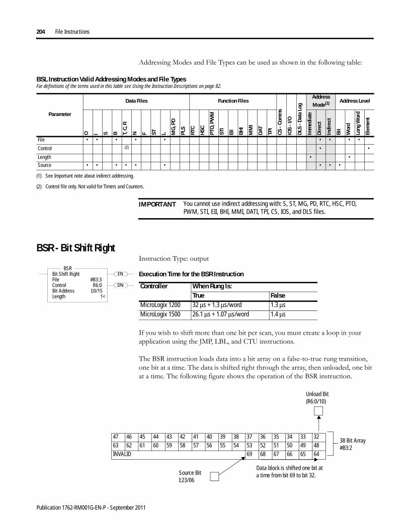
204 File Instructions
Addressing Modes and File Types can be used as shown in the following table:
BSR - Bit Shift RightInstruction Type: output
If you wish to shift more than one bit per scan, you must create a loop in your application using the JMP, LBL, and CTU instructions.
The BSR instruction loads data into a bit array on a false-to-true rung transition, one bit at a time. The data is shifted right through the array, then unloaded, one bit at a time. The following figure shows the operation of the BSR instruction.
BSL Instruction Valid Addressing Modes and File TypesFor definitions of the terms used in this table see Using the Instruction Descriptions on page 82.
Parameter
Data Files Function Files
CS -
Com
ms
IOS
- I/O
DLS
- D
ata
Log
Address Mode(1) Address Level
O I S B T, C
, R
N F ST L MG
, PD
PLS
RTC
HSC
PTO
, PW
M
STI
EII
BHI
MM
I
DAT
TPI
Imm
edia
te
Dir
ect
Indi
rect
Bit
Wor
d
Long
Wor
d
Elem
ent
File • • • • • • • • •
Control (2) • •
Length • •
Source • • • • • • • • •
(1) See Important note about indirect addressing.
(2) Control file only. Not valid for Timers and Counters.
IMPORTANT You cannot use indirect addressing with: S, ST, MG, PD, RTC, HSC, PTO, PWM, STI, EII, BHI, MMI, DATI, TPI, CS, IOS, and DLS files.
EN
DN
BSRBit Shift RightFile #B3:3Control R6:0Bit Address I:0/15Length 1<
BSRExecution Time for the BSR Instruction
Controller When Rung Is:True False
MicroLogix 1200 32 μs + 1.3 μs/word 1.3 μsMicroLogix 1500 26.1 μs + 1.07 μs/word 1.4 μs
Data block is shifted one bit at a time from bit 69 to bit 32.Source Bit
I:23/06
38 Bit Array #B3:2
Unload Bit(R6:0/10)
47 46 45 44 43 42 41 40 39 38 37 36 35 34 33 3263 62 61 60 59 58 57 56 55 54 53 52 51 50 49 48INVALID 69 68 67 66 65 64
Publication 1762-RM001G-EN-P - September 2011

File Instructions 205
This instruction uses the following operands:
• File - The file operand is the address of the bit array that is to be manipulated.
• Control - The control operand is the address of the BSR’s control element. The control element consists of 3 words:
• Bit Address - The source is the address of the bit to be transferred into the bit array at the last (highest) bit position.
• Length - The length operand contains the length of the bit array in bits. The data range for length is from 0 to 2048.
Addressing Modes and File Types can be used as shown in the following table:
15 14 13 12 11 10 9 8 7 6 5 4 3 2 1 0Word 0 EN(1)
(1) EN - Enable Bit is set on false-to-true transition of the rung and indicates the instruction is enabled.
-- DN(2)
(2) DN - Done Bit, when set, indicates that the bit array has shifted one position.
-- ER(3)
(3) ER - Error Bit, when set, indicates that the instruction detected an error such as entering a negative number for the length or source operand.
UL(4)
(4) UL - Unload Bit is the instruction’s output. Avoid using the UL (unload) bit when the ER (error) bit is set.
not used
Word 1 Size of bit array (number of bits).
Word 2 not used
BSR Instruction Valid Addressing Modes and File TypesFor definitions of the terms used in this table see Using the Instruction Descriptions on page 82.
Parameter
Data Files Function Files
CS -
Com
ms
IOS
- I/O
DLS
- D
ata
Log
Address Mode(1) Address Level
O I S B T, C
, R
N F L ST MG
, PD
PLS
RTC
HSC
PTO
, PW
M
STI
EII
BHI
MM
I
DAT
TPI
Imm
edia
te
Dire
ct
Indi
rect
Bit
Wor
d
Long
Wor
d
Elem
ent
File • • • • • • • • •
Control (2) • •
Length • •
Source • • • • • • • • •
(1) See Important note about indirect addressing.
(2) Control file only. Not valid for Timers and Counters.
IMPORTANT You cannot use indirect addressing with: S, ST, MG, PD, RTC, HSC, PTO, PWM, STI, EII, BHI, MMI, DAT, TPI, CS, IOS, and DLS files.
Publication 1762-RM001G-EN-P - September 2011

206 File Instructions
FFL - First In, First Out (FIFO) Load
Instruction Type: output
On a false-to-true rung transition, the FFL instruction loads words or long words into a user-created file called a FIFO stack. This instruction’s counterpart, FIFO unload (FFU), is paired with a given FFL instruction to remove elements from the FIFO stack. Instruction parameters have been programmed in the FFL - FFU instruction pair shown below.
This instruction uses the following operands:
• Source - The source operand is a constant or address of the value used to fill the currently available position in the FIFO stack. The address level of the source must match the FIFO stack. If FIFO is a word size file, source must be a word value or constant. If FIFO is a long word size file, source must be a long word value or constant. The data range for the source is from -32768 to 32767 (word) or -2,147,483,648 to 2,147,483,647 (long word).
EN
DN
EM
FFLFIFO LoadSource N7:0FIFO #N7:1Control R6:0Length 1<Position 0<
FFLExecution Time for the FFL Instruction
Controller Data Size When Rung Is:True False
MicroLogix 1200 word 11.3 μs 11.1 μslong word 11.7 μs 11.2 μs
MicroLogix 1500 word 10.0 μs 9.8 μslong word 10.9 μs 9.7 μs
(EU)
(EM)(DN)
FFLFIFO LOADSource N7:10FIFO #N7:12Control R6:0Length 34Position 9
FFUFIFO UNLOADFIFO #N7:12Dest N7:11Control R6:0Length 34Position 9
(EN)
(DN)(EM)
Destination PositionN7:11 N7:12 0
N7:13 1FFU instruction unloads data from stack #N7:12 at position 0, N7:12
N7:14 2345 34 words are allocated
for FIFO stack starting at N7:12, ending at N7:45
67
Source 8N7:10 9
FFL instruction loads data into stack #N7:12 at the next available position, 9 in this case.
N7:45 33
Loading and Unloading of Stack #N7:12
FFL and FFU Instruction Pair
Publication 1762-RM001G-EN-P - September 2011
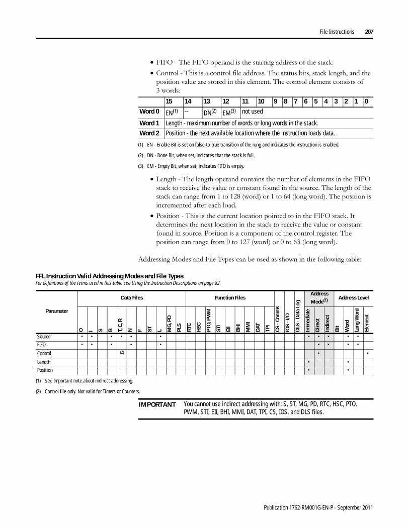
File Instructions 207
• FIFO - The FIFO operand is the starting address of the stack.• Control - This is a control file address. The status bits, stack length, and the
position value are stored in this element. The control element consists of 3 words:
• Length - The length operand contains the number of elements in the FIFO stack to receive the value or constant found in the source. The length of the stack can range from 1 to 128 (word) or 1 to 64 (long word). The position is incremented after each load.
• Position - This is the current location pointed to in the FIFO stack. It determines the next location in the stack to receive the value or constant found in source. Position is a component of the control register. The position can range from 0 to 127 (word) or 0 to 63 (long word).
Addressing Modes and File Types can be used as shown in the following table:
15 14 13 12 11 10 9 8 7 6 5 4 3 2 1 0Word 0 EN(1)
(1) EN - Enable Bit is set on false-to-true transition of the rung and indicates the instruction is enabled.
-- DN(2)
(2) DN - Done Bit, when set, indicates that the stack is full.
EM(3)
(3) EM - Empty Bit, when set, indicates FIFO is empty.
not used
Word 1 Length - maximum number of words or long words in the stack.
Word 2 Position - the next available location where the instruction loads data.
FFL Instruction Valid Addressing Modes and File TypesFor definitions of the terms used in this table see Using the Instruction Descriptions on page 82.
Parameter
Data Files Function Files
CS -
Com
ms
IOS
- I/O
DLS
- D
ata
Log
Address Mode(1) Address Level
O I S B T, C
, R
N F ST L MG
, PD
PLS
RTC
HSC
PTO
, PW
M
STI
EII
BHI
MM
I
DAT
TPI
Imm
edia
te
Dire
ct
Indi
rect
Bit
Wor
d
Long
Wor
d
Elem
ent
Source • • • • • • • • • • •
FIFO • • • • • • • • •
Control (2) • •
Length • •
Position • •
(1) See Important note about indirect addressing.
(2) Control file only. Not valid for Timers or Counters.
IMPORTANT You cannot use indirect addressing with: S, ST, MG, PD, RTC, HSC, PTO, PWM, STI, EII, BHI, MMI, DAT, TPI, CS, IOS, and DLS files.
Publication 1762-RM001G-EN-P - September 2011
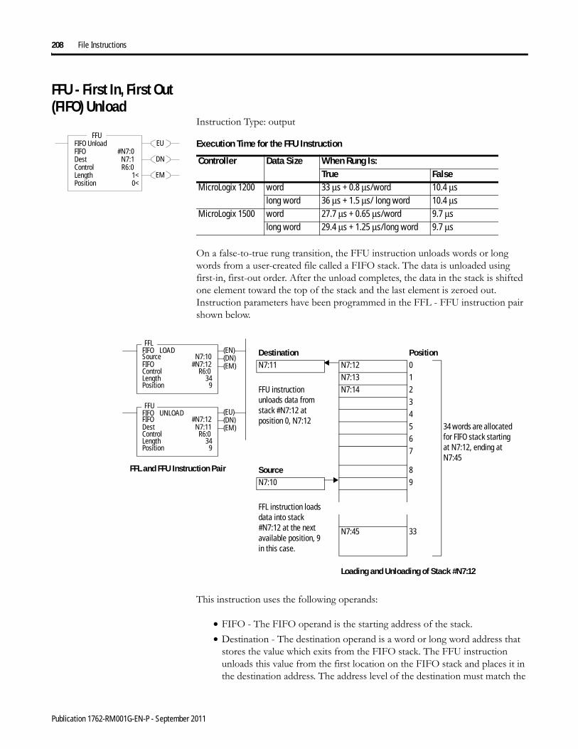
208 File Instructions
FFU - First In, First Out (FIFO) Unload
Instruction Type: output
On a false-to-true rung transition, the FFU instruction unloads words or long words from a user-created file called a FIFO stack. The data is unloaded using first-in, first-out order. After the unload completes, the data in the stack is shifted one element toward the top of the stack and the last element is zeroed out. Instruction parameters have been programmed in the FFL - FFU instruction pair shown below.
This instruction uses the following operands:
• FIFO - The FIFO operand is the starting address of the stack.• Destination - The destination operand is a word or long word address that
stores the value which exits from the FIFO stack. The FFU instruction unloads this value from the first location on the FIFO stack and places it in the destination address. The address level of the destination must match the
EU
DN
EM
FFUFIFO UnloadFIFO #N7:0Dest N7:1Control R6:0Length 1<Position 0<
FFUExecution Time for the FFU Instruction
Controller Data Size When Rung Is:True False
MicroLogix 1200 word 33 μs + 0.8 μs/word 10.4 μslong word 36 μs + 1.5 μs/ long word 10.4 μs
MicroLogix 1500 word 27.7 μs + 0.65 μs/word 9.7 μslong word 29.4 μs + 1.25 μs/long word 9.7 μs
(EU)
(EM)(DN)
FFLFIFO LOADSource N7:10FIFO #N7:12Control R6:0Length 34Position 9
FFUFIFO UNLOADFIFO #N7:12Dest N7:11Control R6:0Length 34Position 9
(EN)
(DN)(EM)
Destination PositionN7:11 N7:12 0
N7:13 1FFU instruction unloads data from stack #N7:12 at position 0, N7:12
N7:14 2345 34 words are allocated
for FIFO stack starting at N7:12, ending at N7:45
67
Source 8N7:10 9
FFL instruction loads data into stack #N7:12 at the next available position, 9 in this case.
N7:45 33
Loading and Unloading of Stack #N7:12
FFL and FFU Instruction Pair
Publication 1762-RM001G-EN-P - September 2011
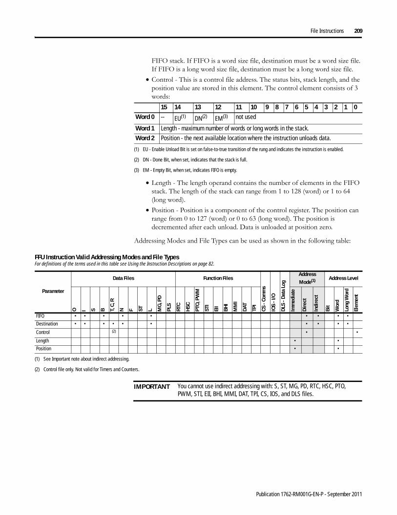
File Instructions 209
FIFO stack. If FIFO is a word size file, destination must be a word size file. If FIFO is a long word size file, destination must be a long word size file.
• Control - This is a control file address. The status bits, stack length, and the position value are stored in this element. The control element consists of 3 words:
• Length - The length operand contains the number of elements in the FIFO stack. The length of the stack can range from 1 to 128 (word) or 1 to 64 (long word).
• Position - Position is a component of the control register. The position can range from 0 to 127 (word) or 0 to 63 (long word). The position is decremented after each unload. Data is unloaded at position zero.
Addressing Modes and File Types can be used as shown in the following table:
15 14 13 12 11 10 9 8 7 6 5 4 3 2 1 0Word 0 -- EU(1)
(1) EU - Enable Unload Bit is set on false-to-true transition of the rung and indicates the instruction is enabled.
DN(2)
(2) DN - Done Bit, when set, indicates that the stack is full.
EM(3)
(3) EM - Empty Bit, when set, indicates FIFO is empty.
not used
Word 1 Length - maximum number of words or long words in the stack.
Word 2 Position - the next available location where the instruction unloads data.
FFU Instruction Valid Addressing Modes and File TypesFor definitions of the terms used in this table see Using the Instruction Descriptions on page 82.
Parameter
Data Files Function Files
CS -
Com
ms
IOS
- I/O
DLS
- D
ata
Log
Address Mode(1) Address Level
O I S B T, C
, R
N F ST L MG
, PD
PLS
RTC
HSC
PTO
, PW
M
STI
EII
BHI
MM
I
DAT
TPI
Imm
edia
te
Dire
ct
Indi
rect
Bit
Wor
d
Long
Wor
d
Elem
ent
FIFO • • • • • • • • •
Destination • • • • • • • • • •
Control (2) • •
Length • •
Position • •
(1) See Important note about indirect addressing.
(2) Control file only. Not valid for Timers and Counters.
IMPORTANT You cannot use indirect addressing with: S, ST, MG, PD, RTC, HSC, PTO, PWM, STI, EII, BHI, MMI, DAT, TPI, CS, IOS, and DLS files.
Publication 1762-RM001G-EN-P - September 2011

210 File Instructions
LFL - Last In, First Out (LIFO) Load
Instruction Type: output
On a false-to-true rung transition, the LFL instruction loads words or long words into a user-created file called a LIFO stack. This instruction’s counterpart, LIFO unload (LFU), is paired with a given LFL instruction to remove elements from the LIFO stack. Instruction parameters have been programmed in the LFL - LFU instruction pair shown below.
This instruction uses the following operands:
• Source - The source operand is a constant or address of the value used to fill the currently available position in the LIFO stack. The data size of the source must match the LIFO stack. If LIFO is a word size file, source must be a word value or constant. If LIFO is a long word size file, source must be a long word value or constant. The data range for the source is from -32768 to 32767 (word) or -2,147,483,648 to 2,147,483,647 (long word).
• LIFO - The LIFO operand is the starting address of the stack.
EN
DN
EM
LFLLIFO LoadSource N7:0LIFO #N7:1Control R6:0Length 1<Position 0<
LFLExecution Time for the LFL Instruction
Controller Data Size When Rung Is:True False
MicroLogix 1200 word 25.5 μs 10.4 μslong word 31.6 μs 10.4 μs
MicroLogix 1500 word 22.2 μs 9.7 μslong word 27.4 μs 9.7 μs
(DN)
(EN)(DN)(EM)
LFLLIFO LOADSource N7:10LIFO #N7:12Control R6:0Length 34Position 9
(EU)
(EM)
LIFO UNLOADLIFO #N7:12Dest N7:11Control R6:0Length 34Position 9
LFU
Destination PositionN7:11 N7:12 0
N7:13 1LFU instruction unloads data from stack #N7:12 at position 0, N7:12
N7:14 2345 34 words are allocated
for FIFO stack starting at N7:12, ending at N7:45
67
Source 8N7:10 9
LFL instruction loads data into stack #N7:12 at the next available position, 9 in this case.
N7:45 33
Loading and Unloading of Stack #N7:12
LFL and LFU Instruction Pair
Publication 1762-RM001G-EN-P - September 2011
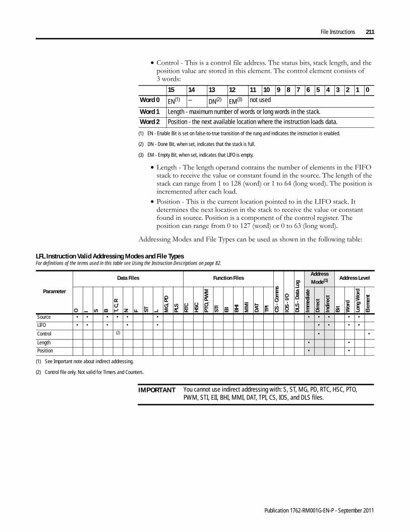
File Instructions 211
• Control - This is a control file address. The status bits, stack length, and the position value are stored in this element. The control element consists of 3 words:
• Length - The length operand contains the number of elements in the FIFO stack to receive the value or constant found in the source. The length of the stack can range from 1 to 128 (word) or 1 to 64 (long word). The position is incremented after each load.
• Position - This is the current location pointed to in the LIFO stack. It determines the next location in the stack to receive the value or constant found in source. Position is a component of the control register. The position can range from 0 to 127 (word) or 0 to 63 (long word).
Addressing Modes and File Types can be used as shown in the following table:
15 14 13 12 11 10 9 8 7 6 5 4 3 2 1 0Word 0 EN(1)
(1) EN - Enable Bit is set on false-to-true transition of the rung and indicates the instruction is enabled.
-- DN(2)
(2) DN - Done Bit, when set, indicates that the stack is full.
EM(3)
(3) EM - Empty Bit, when set, indicates that LIFO is empty.
not used
Word 1 Length - maximum number of words or long words in the stack.
Word 2 Position - the next available location where the instruction loads data.
LFL Instruction Valid Addressing Modes and File TypesFor definitions of the terms used in this table see Using the Instruction Descriptions on page 82.
Parameter
Data Files Function FilesCS
- Co
mm
s
IOS
- I/O
DLS
- D
ata
Log
Address Mode(1) Address Level
O I S B T, C
, R
N F ST L MG
, PD
PLS
RTC
HSC
PTO
, PW
M
STI
EII
BHI
MM
I
DAT
TPI
Imm
edia
te
Dir
ect
Indi
rect
Bit
Wor
d
Long
Wor
d
Elem
ent
Source • • • • • • • • • • •
LIFO • • • • • • • • •
Control (2) • •
Length • •
Position • •
(1) See Important note about indirect addressing.
(2) Control file only. Not valid for Timers and Counters.
IMPORTANT You cannot use indirect addressing with: S, ST, MG, PD, RTC, HSC, PTO, PWM, STI, EII, BHI, MMI, DAT, TPI, CS, IOS, and DLS files.
Publication 1762-RM001G-EN-P - September 2011

212 File Instructions
LFU - Last In, First Out (LIFO) Unload
Instruction Type: output
On a false-to-true rung transition, the LFU instruction unloads words or long words from a user-created file called a LIFO stack. The data is unloaded using last-in, first-out order. Instruction parameters have been programmed in the LFL - LFU instruction pair shown below.
This instruction uses the following operands:
• LIFO - The LIFO operand is the starting address of the stack.• Destination - The destination operand is a word or long word address that
stores the value which exits from the LIFO stack. The LFU instruction unloads this value from the last location on the LIFO stack and places it in the destination address. The address level of the destination must match the LIFO stack. If LIFO is a word size file, destination must be a word size file. If LIFO is a long word size file, destination must be a long word size file.
EU
DN
EM
LFULIFO UnloadLIFO #N7:0Dest N7:1Control R6:0Length 1<Position 0<
LFUExecution Time for the LFU Instruction
Controller Data Size When Rung Is:True False
MicroLogix 1200 word 29.1 μs 10.4 μslong word 31.6 μs 10.4 μs
MicroLogix 1500 word 25.6 μs 9.7 μslong word 27.4 μs 9.7 μs
(DN)
(EN)(DN)(EM)
LFLLIFO LOADSource N7:10LIFO #N7:12Control R6:0Length 34Position 9
(EU)
(EM)
LIFO UNLOADLIFO #N7:12Dest N7:11Control R6:0Length 34Position 9
LFU
Destination PositionN7:11 N7:12 0
N7:13 1LFU instruction unloads data from stack #N7:12 at position 0, N7:12
N7:14 2345 34 words are allocated
for FIFO stack starting at N7:12, ending at N7:45
67
Source 8N7:10 9
LFL instruction loads data into stack #N7:12 at the next available position, 9 in this case.
N7:45 33
Loading and Unloading of Stack #N7:12
LFL and LFU Instruction Pair
Publication 1762-RM001G-EN-P - September 2011
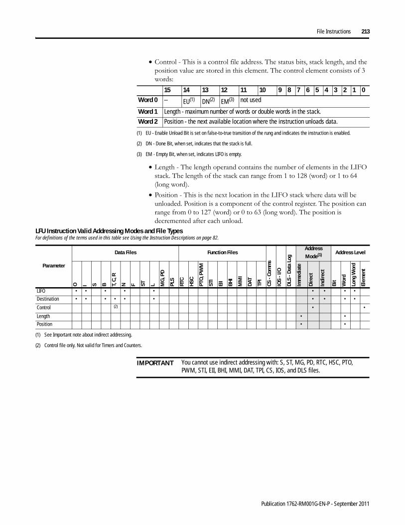
File Instructions 213
• Control - This is a control file address. The status bits, stack length, and the position value are stored in this element. The control element consists of 3 words:
• Length - The length operand contains the number of elements in the LIFO stack. The length of the stack can range from 1 to 128 (word) or 1 to 64 (long word).
• Position - This is the next location in the LIFO stack where data will be unloaded. Position is a component of the control register. The position can range from 0 to 127 (word) or 0 to 63 (long word). The position is decremented after each unload.
15 14 13 12 11 10 9 8 7 6 5 4 3 2 1 0Word 0 -- EU(1)
(1) EU - Enable Unload Bit is set on false-to-true transition of the rung and indicates the instruction is enabled.
DN(2)
(2) DN - Done Bit, when set, indicates that the stack is full.
EM(3)
(3) EM - Empty Bit, when set, indicates LIFO is empty.
not used
Word 1 Length - maximum number of words or double words in the stack.
Word 2 Position - the next available location where the instruction unloads data.
LFU Instruction Valid Addressing Modes and File TypesFor definitions of the terms used in this table see Using the Instruction Descriptions on page 82.
Parameter
Data Files Function Files
CS -
Com
ms
IOS
- I/O
DLS
- D
ata
Log
Address Mode(1) Address Level
O I S B T, C
, R
N F ST L MG
, PD
PLS
RTC
HSC
PTO
, PW
M
STI
EII
BHI
MM
I
DAT
TPI
Imm
edia
te
Dir
ect
Indi
rect
Bit
Wor
d
Long
Wor
d
Elem
ent
LIFO • • • • • • • • •
Destination • • • • • • • • • •
Control (2) • •
Length • •
Position • •
(1) See Important note about indirect addressing.
(2) Control file only. Not valid for Timers and Counters.
IMPORTANT You cannot use indirect addressing with: S, ST, MG, PD, RTC, HSC, PTO, PWM, STI, EII, BHI, MMI, DAT, TPI, CS, IOS, and DLS files.
Publication 1762-RM001G-EN-P - September 2011
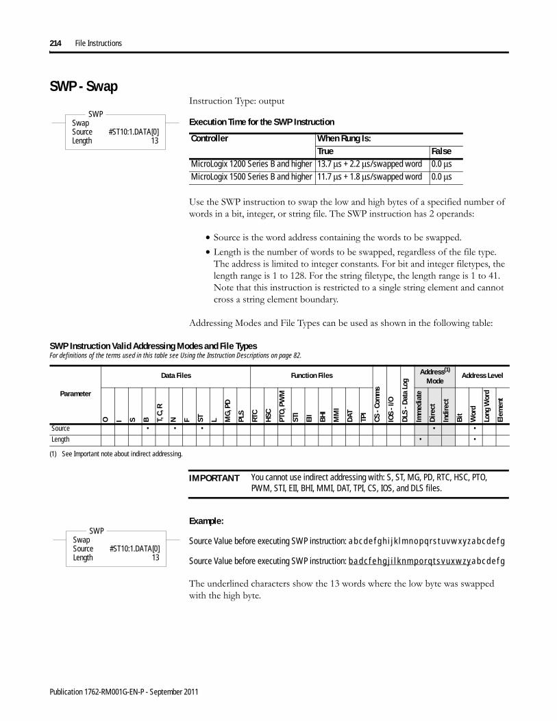
214 File Instructions
SWP - SwapInstruction Type: output
Use the SWP instruction to swap the low and high bytes of a specified number of words in a bit, integer, or string file. The SWP instruction has 2 operands:
• Source is the word address containing the words to be swapped.• Length is the number of words to be swapped, regardless of the file type.
The address is limited to integer constants. For bit and integer filetypes, the length range is 1 to 128. For the string filetype, the length range is 1 to 41. Note that this instruction is restricted to a single string element and cannot cross a string element boundary.
Addressing Modes and File Types can be used as shown in the following table:
Example:
Source Value before executing SWP instruction: a b c d e f g h i j k l m n o p q r s t u v w x y z a b c d e f g
Source Value before executing SWP instruction: b a d c f e h g j i l k n m p o r q t s v u x w z y a b c d e f g
The underlined characters show the 13 words where the low byte was swapped with the high byte.
SWPSwapSource #ST10:1.DATA[0]Length 13
SWPExecution Time for the SWP Instruction
Controller When Rung Is:True False
MicroLogix 1200 Series B and higher 13.7 μs + 2.2 μs/swapped word 0.0 μsMicroLogix 1500 Series B and higher 11.7 μs + 1.8 μs/swapped word 0.0 μs
SWP Instruction Valid Addressing Modes and File TypesFor definitions of the terms used in this table see Using the Instruction Descriptions on page 82.
Parameter
Data Files Function FilesCS
- Co
mm
s
IOS
- I/O
DLS
- D
ata
Log
Address(1) Mode
Address Level
O I S B T, C
, R
N F ST L MG
, PD
PLS
RTC
HSC
PTO
, PW
M
STI
EII
BHI
MM
I
DAT
TPI
Imm
edia
te
Dire
ct
Indi
rect
Bit
Wor
d
Long
Wor
d
Elem
ent
Source • • • • •
Length • •
(1) See Important note about indirect addressing.
IMPORTANT You cannot use indirect addressing with: S, ST, MG, PD, RTC, HSC, PTO, PWM, STI, EII, BHI, MMI, DAT, TPI, CS, IOS, and DLS files.
SWPSwapSource #ST10:1.DATA[0]Length 13
SWP
Publication 1762-RM001G-EN-P - September 2011

Chapter 15
Sequencer Instructions
Sequencer instructions are used to control automatic assembly machines or processes that have a consistent and repeatable operation. They are typically time based or event driven.
Use the sequencer compare instruction to detect when a step is complete; use the sequencer output instruction to set output conditions for each step. Use the sequencer load instruction to load data into the sequencer file.
The primary advantage of sequencer instructions is to conserve program memory. These instructions monitor and control 16 (word) or 32 (long word) discrete outputs at a time in a single rung.
You can use bit integer or double integer files with sequencer instructions.
SQC- Sequencer Compare
Instruction Type: output
On a false-to-true rung transition, the SQC instruction is used to compare masked source words or long words with the masked value at a reference address (the sequencer file) for the control of sequential machine operations.
When the status of all non-masked bits in the source word match those of the corresponding reference word, the instruction sets the found bit (FD) in the control word. Otherwise, the found bit (FD) is cleared.
Instruction Used To: Page
SQC - Sequencer Compare Compare 16-bit data with stored data 215
SQO - Sequencer Output Transfer 16-bit data to word addresses 218
SQL - Sequencer Load Load 16-bit data into a file 221
EN
DN
FD
SQCSequencer CompareFile #B3:0Mask N7:0Source I:0.0Control R6:0Length 1<Position 0<
SQCExecution Time for the SQC Instruction
Controller Data Size When Rung Is:True False
MicroLogix 1200 word 23.5 μs 7.1 μslong word 26.3 μs 7.1 μs
MicroLogix 1500 word 20.1 μs 6.3 μslong word 22.7 μs 6.3 μs
215 Publication 1762-RM001G-EN-P - September 2011
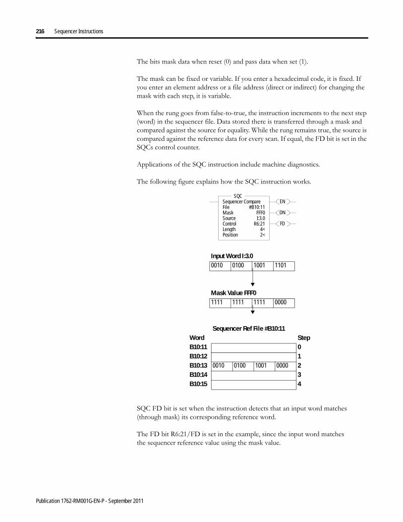
216 Sequencer Instructions
The bits mask data when reset (0) and pass data when set (1).
The mask can be fixed or variable. If you enter a hexadecimal code, it is fixed. If you enter an element address or a file address (direct or indirect) for changing the mask with each step, it is variable.
When the rung goes from false-to-true, the instruction increments to the next step (word) in the sequencer file. Data stored there is transferred through a mask and compared against the source for equality. While the rung remains true, the source is compared against the reference data for every scan. If equal, the FD bit is set in the SQCs control counter.
Applications of the SQC instruction include machine diagnostics.
The following figure explains how the SQC instruction works.
SQC FD bit is set when the instruction detects that an input word matches (through mask) its corresponding reference word.
The FD bit R6:21/FD is set in the example, since the input word matches the sequencer reference value using the mask value.
EN
DN
FD
SQCSequencer CompareFile #B10:11Mask FFF0Source I:3.0Control R6:21Length 4<Position 2<
SQC
Input Word I:3.00010 0100 1001 1101
Mask Value FFF01111 1111 1111 0000
Sequencer Ref File #B10:11Word StepB10:11 0B10:12 1B10:13 0010 0100 1001 0000 2B10:14 3B10:15 4
Publication 1762-RM001G-EN-P - September 2011

Sequencer Instructions 217
This instruction uses the following operands:
• File - This is the sequencer reference file. Its contents, on an element-by-element basis, are masked and compared to the masked value stored in source.
• Mask - The mask operand contains the mask constant, word, or file which is applied to both file and source. When mask bits are set to 1, data is allowed to pass through for comparison. When mask bits are reset to 0, the data is masked (does not pass through to for comparison). The immediate data ranges for mask are from 0 to 0xFFFF or 0 to 0xFFFFFFFF.
• Source - This is the value that is compared to file.• Control - This is a control file address. The status bits, stack length, and the
position value are stored in this element. The control element consists of 3 words:
• Length - The length operand contains the number of steps in the sequencer file (as well as Mask and/or Source if they are file data types). The length of the sequencer can range from 1 to 256.
• Position - This is the current location or step in the sequencer file (as well as Mask and/or Source if they are file data types). It determines the next location in the stack to receive the current comparison data. Position is a component of the control register. The position can range from 0 to 255 for words and 0 to 127 for long words. The position is incremented on each false-to-true transition.
TIP If file type is word, then mask and source must be words. If file type is long word, mask and source must be long words.
TIP If mask is direct or indirect, the position selects the location in the specified file.
15 14 13 12 11 10 9 8 7 6 5 4 3 2 1 0Word 0 EN(1)
(1) EN - Enable Bit is set by a false-to-true rung transition and indicates that the instruction is enabled.
-- DN(2)
(2) DN - Done Bit is set after the instruction has operated on the last word in the sequencer file. It is reset on the next false-to-true rung transition after the rung goes false.
-- ER(3)
(3) ER - Error Bit is set when the controller detects a negative position value, or a negative or zero length value. When the ER bit is set, the minor error bit (S2:5/2) is also set.
not used FD(4)
(4) FD - Found bit is set when the status of all non-masked bits in the source address match those of the word in the sequencer reference file. This bit is assessed each time the SQC instruction is evaluated while the rung is true.
not used
Word 1 Length - contains the number of steps in the sequencer reference file.
Word 2 Position - the current position in the sequence
Publication 1762-RM001G-EN-P - September 2011
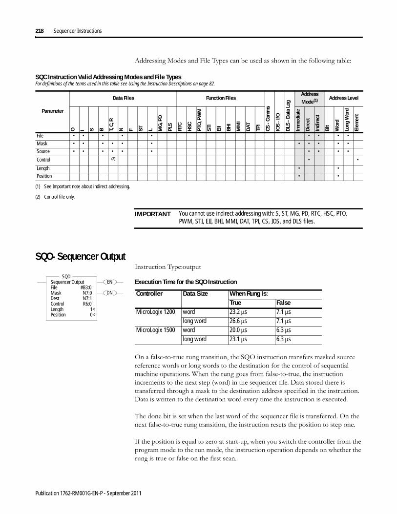
218 Sequencer Instructions
Addressing Modes and File Types can be used as shown in the following table:
SQO- Sequencer OutputInstruction Type:output
On a false-to-true rung transition, the SQO instruction transfers masked source reference words or long words to the destination for the control of sequential machine operations. When the rung goes from false-to-true, the instruction increments to the next step (word) in the sequencer file. Data stored there is transferred through a mask to the destination address specified in the instruction. Data is written to the destination word every time the instruction is executed.
The done bit is set when the last word of the sequencer file is transferred. On the next false-to-true rung transition, the instruction resets the position to step one.
If the position is equal to zero at start-up, when you switch the controller from the program mode to the run mode, the instruction operation depends on whether the rung is true or false on the first scan.
SQC Instruction Valid Addressing Modes and File TypesFor definitions of the terms used in this table see Using the Instruction Descriptions on page 82.
Parameter
Data Files Function Files
CS -
Com
ms
IOS
- I/O
DLS
- D
ata
Log
Address Mode(1) Address Level
O I S B T, C
, R
N F ST L MG
, PD
PLS
RTC
HSC
PTO
, PW
M
STI
EII
BHI
MM
I
DAT
TPI
Imm
edia
te
Dir
ect
Indi
rect
Bit
Wor
d
Long
Wor
d
Elem
ent
File • • • • • • • • •
Mask • • • • • • • • • • •
Source • • • • • • • • • •
Control (2) • •
Length • •
Position • •
(1) See Important note about indirect addressing.
(2) Control file only.
IMPORTANT You cannot use indirect addressing with: S, ST, MG, PD, RTC, HSC, PTO, PWM, STI, EII, BHI, MMI, DAT, TPI, CS, IOS, and DLS files.
EN
DN
SQOSequencer OutputFile #B3:0Mask N7:0Dest N7:1Control R6:0Length 1<Position 0<
SQOExecution Time for the SQO Instruction
Controller Data Size When Rung Is:True False
MicroLogix 1200 word 23.2 μs 7.1 μslong word 26.6 μs 7.1 μs
MicroLogix 1500 word 20.0 μs 6.3 μslong word 23.1 μs 6.3 μs
Publication 1762-RM001G-EN-P - September 2011

Sequencer Instructions 219
• If the rung is true, the instruction transfers the value in step zero.• If the rung is false, the instruction waits for the first rung transition
from false-to-true and transfers the value in step one.
The bits mask data when reset (0) and pass data when set (1). The instruction will not change the value in the destination word unless you set mask bits.
The mask can be fixed or variable. It is fixed if you enter a hexadecimal code. It is variable if you enter an element address or a file address (direct or indirect) for changing the mask with each step.
The following figure indicates how the SQO instruction works.
Destination O:14.0 External Outputs (O:14) at Step 2
15 8 7 0 000000 0101 0000 1010 01 ON
02Mask Value 0F0F 03 ON15 8 7 0 040000 1111 0000 1111 05
06Sequencer Output File #B10:1 07
Word Step 08 ONB10:1 0000 0000 0000 0000 0 09B10:2 1010 0010 1111 0101 1 10 ONB10:3 1111 0101 0100 1010 2 Current Step 11B10:4 0101 0101 0101 0101 3 12B10:5 0000 1111 0000 1111 4 13
1415
EN
DN
SQOSequencer OutputFile #B10:1Mask 0F0FDest O14:0Control R6:20Length 4<Position 2<
SQO
Publication 1762-RM001G-EN-P - September 2011

220 Sequencer Instructions
This instruction uses the following operands:
• File - This is the sequencer reference file. Its contents, on an element-by-element, basis are masked and stored in the destination.
• Mask - The mask operand contains the mask value. When mask bits are set to 1, data is allowed to pass through to destination. When mask bits are reset to 0, the data is masked (does not pass through to destination). The immediate data ranges for mask are from 0 to 0xFFFF (word) or 0 to 0xFFFFFFFF (long word).
• Destination - The destination operand is the sequencer location or file.• Control - This is a control file address. The status bits, stack length, and the
position value are stored in this element. The control element consists of 3 words:
• Length - The length operand contains the number of steps in the sequencer file (as well as Mask and/or Destination if they are file data types). The length of the sequencer can range from 1 to 256.
• Position - This is the current location or step in the sequencer file (as well as Mask and/or Destination if they are file data types). It determines the next location in the stack to be masked and moved to the destination. Position is a component of the control register. The position can range from 0 to 255. Position is incremented on each false-to-true transition.
Addressing Modes and File Types can be used as shown in the following table:
TIP If file type is word, then mask and source must be words. If file type is long word, mask and source must be long words.
TIP If mask is direct or indirect, the position selects the location in the specified file.
15 14 13 12 11 10 9 8 7 6 5 4 3 2 1 0Word 0 EN(1)
(1) EN - Enable Bit is set by a false-to-true rung transition and indicates that the instruction is enabled.
-- DN(2)
(2) DN - Done Bit is set after the instruction has operated on the last word in the sequencer file. It is reset on the next false-to-true rung transition after the rung goes false.
-- ER(3)
(3) ER - Error Bit is set when the controller detects a negative position value, or a negative or zero length value. When the ER bit is set, the minor error bit (S2:5/2) is also set.
not used FD not used
Word 1 Length - contains the index of the last element in the sequencer reference file
Word 2 Position - the current position in the sequence
SQO Instruction Valid Addressing Modes and File TypesFor definitions of the terms used in this table see Using the Instruction Descriptions on page 82.
Parameter
Data Files Function Files
CS -
Com
ms
IOS
- I/O
DLS
- D
ata
Log
Address
Mode(1) Address Level
O I S B T, C
, R
N F ST L MG
, PD
PLS
RTC
HSC
PTO
, PW
M
STI
EII
BHI
MM
I
DAT
TPI
Imm
edia
te
Dire
ct
Indi
rect
Elem
ent
Bit
Wor
d
Long
Wor
d
File(2) • • • • • • • • •
Publication 1762-RM001G-EN-P - September 2011
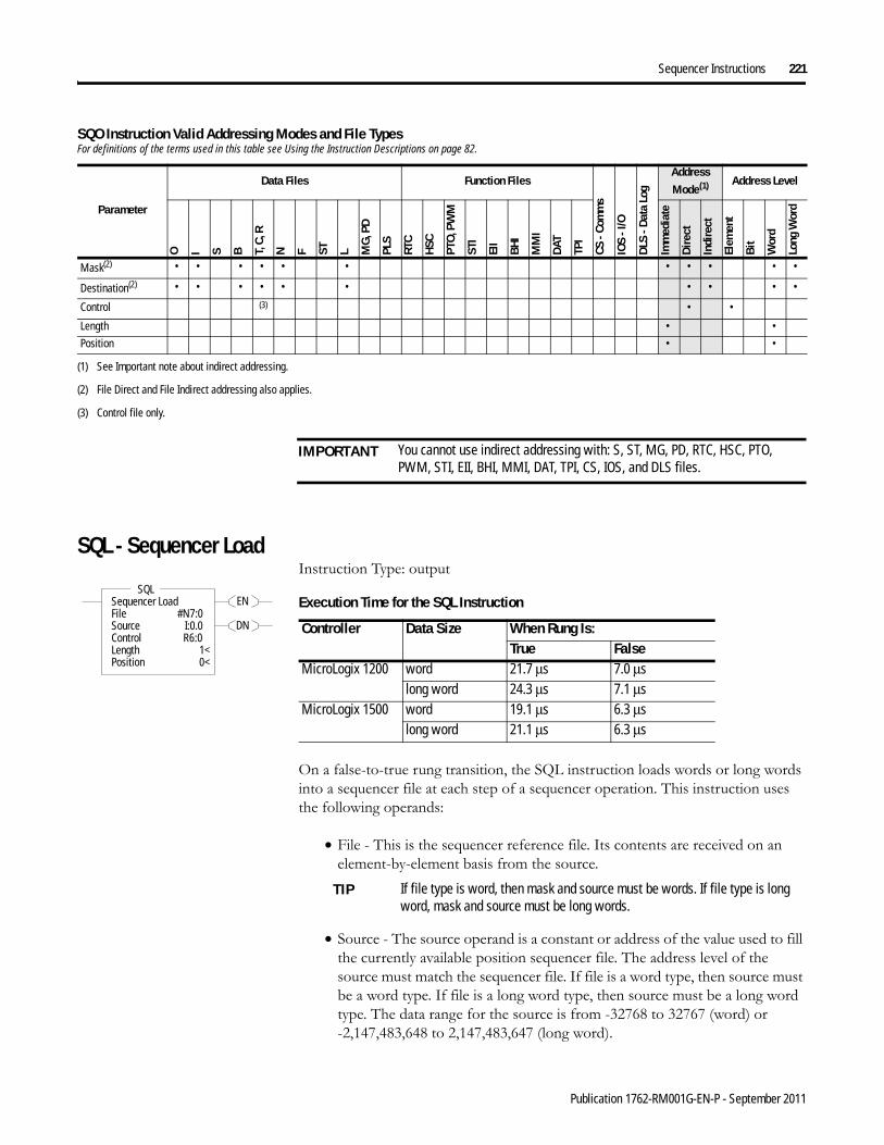
Sequencer Instructions 221
SQL - Sequencer LoadInstruction Type: output
On a false-to-true rung transition, the SQL instruction loads words or long words into a sequencer file at each step of a sequencer operation. This instruction uses the following operands:
• File - This is the sequencer reference file. Its contents are received on an element-by-element basis from the source.
• Source - The source operand is a constant or address of the value used to fill the currently available position sequencer file. The address level of the source must match the sequencer file. If file is a word type, then source must be a word type. If file is a long word type, then source must be a long word type. The data range for the source is from -32768 to 32767 (word) or -2,147,483,648 to 2,147,483,647 (long word).
Mask(2) • • • • • • • • • • •
Destination(2) • • • • • • • • • •
Control (3) • •
Length • •
Position • •
(1) See Important note about indirect addressing.
(2) File Direct and File Indirect addressing also applies.
(3) Control file only.
SQO Instruction Valid Addressing Modes and File TypesFor definitions of the terms used in this table see Using the Instruction Descriptions on page 82.
Parameter
Data Files Function Files
CS -
Com
ms
IOS
- I/O
DLS
- Da
ta L
og
Address
Mode(1) Address LevelO I S B T,
C, R
N F ST L MG
, PD
PLS
RTC
HSC
PTO
, PW
M
STI
EII
BHI
MM
I
DAT
TPI
Imm
edia
te
Dire
ct
Indi
rect
Elem
ent
Bit
Wor
d
Long
Wor
d
IMPORTANT You cannot use indirect addressing with: S, ST, MG, PD, RTC, HSC, PTO, PWM, STI, EII, BHI, MMI, DAT, TPI, CS, IOS, and DLS files.
EN
DN
SQLSequencer LoadFile #N7:0Source I:0.0Control R6:0Length 1<Position 0<
SQLExecution Time for the SQL Instruction
Controller Data Size When Rung Is:True False
MicroLogix 1200 word 21.7 μs 7.0 μslong word 24.3 μs 7.1 μs
MicroLogix 1500 word 19.1 μs 6.3 μslong word 21.1 μs 6.3 μs
TIP If file type is word, then mask and source must be words. If file type is long word, mask and source must be long words.
Publication 1762-RM001G-EN-P - September 2011

222 Sequencer Instructions
• Control - This is a control file address. The status bits, stack length, and the position value are stored in this element. The control element consists of 3 words:
• Length - The length operand contains the number of steps in the sequencer file (this is also the length of source if it is a file data type). The length of the sequencer can range from 1 to 256.
• Position - This is the current location or step in the sequencer file (as well as source if it is a file data type). It determines the next location in the stack to receive the value or constant found in source. Position is a component of the control register. The position can range from 0 to 255.
Addressing Modes and File Types can be used as shown in the following table:
15 14 13 12 11 10 9 8 7 6 5 4 3 2 1 0Word 0 EN(1)
(1) EN - Enable Bit is set by a false-to-true rung transition and indicates that the instruction is enabled.
-- DN(2)
(2) DN - Done Bit is set after the instruction has operated on the last word in the sequencer file. It is reset on the next false-to-true rung transition after the rung goes false.
-- ER(3)
(3) ER - Error Bit is set when the controller detects a negative position value, or a negative or zero length value. When the ER bit is set, the minor error bit (S2:5/2) is also set.
not used FD not used
Word 1 Length - contains the index of the last element in the sequencer reference file
Word 2 Position - the current position in the sequence
SQL Instruction Valid Addressing Modes and File TypesFor definitions of the terms used in this table see Using the Instruction Descriptions on page 82.
Parameter
Data Files Function Files
CS -
Com
ms
IOS
- I/O
DLS
- D
ata
Log
Address Mode(1) Address Level
O I S B T, C
, R
N F ST L MG
, PD
PLS
RTC
HSC
PTO
, PW
M
STI
EII
BHI
MM
I
DAT
TPI
Imm
edia
te
Dire
ct
Indi
rect
Bit
Wor
d
Long
Wor
d
Elem
ent
File(2) • • • • • • • • •
Source(2) • • • • • • • • • •
Control (3) • •
Length • •
Position • •
(1) See Important note about indirect addressing.
(2) File Direct and File Indirect addressing also applies.
(3) Control file only.
IMPORTANT You cannot use indirect addressing with: S, ST, MG, PD, RTC, HSC, PTO, PWM, STI, EII, BHI, MMI, DAT, TPI, CS, IOS, and DLS files.
Publication 1762-RM001G-EN-P - September 2011

Chapter 16
Program Control Instructions
Use these instructions to change the order in which the processor scans a ladder program. Typically these instructions are used to minimize scan time, create a more efficient program, and troubleshoot a ladder program.
JMP - Jump to LabelInstruction Type: output
The JMP instruction causes the controller to change the order of ladder execution. Jumps cause program execution to go to the rung marked LBL label number. Jumps can be forward or backward in ladder logic within the same program file. Multiple JMP instructions may cause execution to proceed to the same label.
The immediate data range for the label is from 0 to 999. The label is local to a program file.
Instruction Used To: Page
JMP - Jump to Label Jump forward/backward to a corresponding label instruction
223
LBL - Label 224
JSR - Jump to Subroutine Jump to a designated subroutine and return 224
SBR - Subroutine Label 224
RET - Return from Subroutine 225
SUS - Suspend Debug or diagnose your user program 225
TND - Temporary End Abort current ladder scan 225
END - Program End End a program or subroutine 226
MCR - Master Control Reset Enable or inhibit a master control zone in your ladder program
226
JMPQ2:0
Execution Time for the JMP Instruction
Controller When Rung Is:True False
MicroLogix 1200 1.0 μs 0.0 μsMicroLogix 1500 1.0 μs 0.0 μs
223 Publication 1762-RM001G-EN-P - September 2011

224 Program Control Instructions
LBL - LabelInstruction Type: input
The LBL instruction is used in conjunction with a jump (JMP) instruction to change the order of ladder execution. Jumps cause program execution to go to the rung marked LBL label number.
The immediate data range for the label is from 0 to 999. The label is local to a program file.
JSR - Jump to Subroutine
Instruction Type: output
The JSR instruction causes the controller to start executing a separate subroutine file within a ladder program. JSR moves program execution to the designated subroutine (SBR file number). After executing the SBR, control proceeds to the instruction following the JSR instruction.
The immediate data range for the JSR file is from 3 to 255.
SBR - Subroutine LabelInstruction Type: input
LBLQ2:0
Execution Time for the LBL Instruction
Controller When Rung Is:True False
MicroLogix 1200 1.0 μs 1.0 μsMicroLogix 1500 1.0 μs 1.0 μs
JSRJump To SubroutineSBR File Number U:255
JSRExecution Time for the JSR Instruction
Controller When Rung Is:True False
MicroLogix 1200 8.4 μs 0.0 μsMicroLogix 1500 8.0 μs 0.0 μs
SBRSubroutine
SBRExecution Time for the SBR Instruction
Controller When Rung Is:True False
MicroLogix 1200 1.0 μs 1.0 μsMicroLogix 1500 1.0 μs 1.0 μs
Publication 1762-RM001G-EN-P - September 2011

Program Control Instructions 225
The SBR instruction is a label which is not used by the processor. It is for user subroutine identification purposes as the first rung for that subroutine. This instruction is the first instruction on a rung and is always evaluated as true.
RET - Return from Subroutine
Instruction Type: output
The RET instruction marks the end of subroutine execution or the end of the subroutine file. It causes the controller to resume execution at the instruction following the JSR instruction, user interrupt, or user fault routine that caused this subroutine to execute.
SUS - SuspendInstruction Type: output
The SUS instruction is used to trap and identify specific conditions for program debugging and system troubleshooting. This instruction causes the processor to enter the suspend idle mode, causing all outputs to be de-energized. The suspend ID and the suspend file (program file number or subroutine file number identifying where the suspend instruction resides) are placed in the status file (S:7 and S:8).
The immediate data range for the suspend ID is from -32768 to 32767.
TND - Temporary EndInstruction Type: output
RETReturn
RETExecution Time for the RET Instruction
Controller When Rung Is:True False
MicroLogix 1200 1.0 μs 0.0 μsMicroLogix 1500 1.0 μs 0.0 μs
SUSSuspendSuspend ID 1
SUS
TNDExecution Time for the TND Instruction
Controller When Rung Is:True False
MicroLogix 1200 0.9 μs 0.0 μsMicroLogix 1500 1.0 μs 0.0 μs
Publication 1762-RM001G-EN-P - September 2011

226 Program Control Instructions
The TND instruction is used to denote a premature end-of-ladder program execution. The TND instruction cannot be executed from a STI subroutine, HSC subroutine, EII subroutine, or a user fault subroutine. This instruction may appear more than once in a ladder program.
On a true rung, TND stops the processor from scanning the rest of the program file. In addition, this instruction performs the output scan, input scan, and housekeeping aspects of the processor scan cycle prior to resuming scanning at rung 0 of the main program (file 2). If this instruction is executed in a nested subroutine, it terminates execution of all nested subroutines.
END - Program EndInstruction Type: output
The END instruction must appear at the end of every ladder program. For the main program file (file 2), this instruction ends the program scan. For a subroutine, interrupt, or user fault file, the END instruction causes a return from subroutine.
MCR - Master Control Reset
Instruction Type: output
The MCR instruction works in pairs to control the ladder logic found between those pairs. Rungs within the MCR zone are still scanned, but scan time is reduced due to the false state of non-retentive outputs. Non-retentive outputs are reset when the rung goes false.
This instruction defines the boundaries of an MCR Zone. An MCR Zone is the set of ladder logic instructions bounded by an MCR instruction pair. The start of an MCR zone is defined to be the rung that contains an MCR instruction preceded by conditional logic. The end of an MCR zone is defined to be the first rung containing just an MCR instruction following a start MCR zone rung as shown below.
END
MCRExecution Time for the MCR Instructions
Controller Instruction When Rung Is:True False
MicroLogix 1200 MCR Start 1.2 μs 1.2 μsMCR End 1.6 μs 1.6 μs
MicroLogix 1500 MCR Start 0.8 μs 0.8 μsMCR End 1.0 μs 1.0 μs
Publication 1762-RM001G-EN-P - September 2011

Program Control Instructions 227
While the rung state of the first MCR instruction is true, execution proceeds as if the zone were not present. When the rung state of the first MCR instruction is false, the ladder logic within the MCR zone is executed as if the rung is false. All non-retentive outputs within the MCR zone are reset.
MCR zones let you enable or inhibit segments of your program, such as for recipe applications.
When you program MCR instructions, note that:
• You must end the zone with an unconditional MCR instruction.• You cannot nest one MCR zone within another.• Do not jump into an MCR zone. If the zone is false, jumping into it activates
the zone.
TIP The MCR instruction is not a substitute for a hard-wired master control relay that provides emergency stop capability. You still must install a hard-wired master control relay to provide emergency I/O power shutdown.
If you start instructions such as timers or counters in an MCR zone, instruction operation ceases when the zone is disabled. Re-program critical operations outside the zone if necessary.
0030I:1
0MCR
0031
0032
0033 MCR
Ladder Logic within MCR Zone
Publication 1762-RM001G-EN-P - September 2011

228 Program Control Instructions
Notes:
Publication 1762-RM001G-EN-P - September 2011

Chapter 17
Input and Output Instructions
The input and output instructions allow you to selectively update data without waiting for the input and output scans.
IIM - Immediate Input with Mask
Instruction Type: output
The IIM instruction allows you to selectively update input data without waiting for the automatic input scan. This instruction uses the following operands:
• Slot - This operand defines the location where data is obtained for updating the input file. The location specifies the slot number and the word where data is to be obtained. For example, if slot = I:0, input data from slot 0 starting at word 0 is masked and placed in input data file I:0 starting at word 0 for the specified length. If slot = I0.1, word 1 of slot 0 is used, and so on.
• Mask - The mask is a hex constant or register address containing the mask value to be applied to the slot. If a given bit position in the mask is a “1”, the
Instruction Used To: Page
IIM - Immediate Input with Mask Update data prior to the normal input scan. 229
IOM - Immediate Output with Mask
Update outputs prior to the normal output scan. 230
REF - I/O Refresh Interrupt the program scan to execute the I/O scan (write outputs, service communications, read inputs)
231
IIMImmediate Input w/MaskSlot I:0.0Mask N7:0Length 1
IIM
TIP This instruction is used for embedded I/O only. It is not designed to be used with expansion I/O.
Execution Time for the IIM Instruction
Controller When Rung Is:True False
MicroLogix 1200 26.4 μs 0.0 μsMicroLogix 1500 22.5 μs 0.0 μs
IMPORTANT Slot 0 is the only valid slot number that can be used with this instruction. IIM cannot be used with expansion I/O.
229 Publication 1762-RM001G-EN-P - September 2011

230 Input and Output Instructions
corresponding bit data from slot is passed to the input data file. A “0” prohibits corresponding bit data in slot from being passed to the input data file. The mask value can range from 0 to 0xFFFF.
• Length - This is the number of masked words to transfer to the input data file.
Addressing Modes and File Types can be used as shown below:
IOM - Immediate Output with Mask
Instruction Type: output
The IOM instruction allows you to selectively update output data without waiting for the automatic output scan. This instruction uses the following operands:
• Slot - The slot is the physical location that is updated with data from the output file.
Bit 15 14 13 12 11 10 9 8 7 6 5 4 3 2 1 0Real Input Input Word
Mask 0 0 0 0 0 0 0 0 1 1 1 1 1 1 1 1
Input Data File
Data is Not Updated Updated to Match Input Word
IIM Instruction Valid Addressing Modes and File TypesFor definitions of the terms used in this table see Using the Instruction Descriptions on page 82.
Parameter
Data Files Function Files
CS -
Com
ms
IOS
- I/O
DLS
- D
ata
Log
Address Mode
Address Level
O I S B T, C
, R
N F ST L MG
, PD
PLS
RTC
HSC
PTO
, PW
M
STI
EII
BHI
MM
I
DAT
TPI
Imm
edia
te
Dire
ct
Indi
rect
Bit
Wor
d
Long
Wor
d
Elem
ent
Slot • • •
Mask • • • • • • • • •
Length •
IOMImmediate Output w/MaskSlot O:0.0Mask N7:0Length 1
IOM
TIP This instruction is used for embedded I/O only. It is not designed to be used with expansion I/O.
Execution Time for the IOM Instruction
Controller When Rung Is:True False
MicroLogix 1200 22.3 μs 0.0 μsMicroLogix 1500 1764-LSP 18.4 μs 0.0 μsMicroLogix 1500 1764-LRP 19.4 μs 0.0 μs
IMPORTANT Slot 0 is the only valid slot number that can be used with this instruction. IOM cannot be used with expansion I/O.
Publication 1762-RM001G-EN-P - September 2011
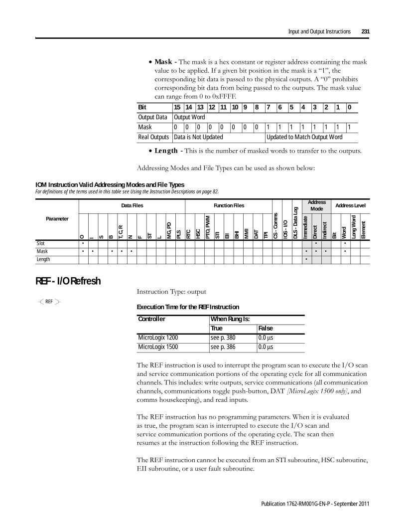
Input and Output Instructions 231
• Mask - The mask is a hex constant or register address containing the mask value to be applied. If a given bit position in the mask is a “1”, the corresponding bit data is passed to the physical outputs. A “0” prohibits corresponding bit data from being passed to the outputs. The mask value can range from 0 to 0xFFFF.
• Length - This is the number of masked words to transfer to the outputs.
Addressing Modes and File Types can be used as shown below:
REF - I/O RefreshInstruction Type: output
The REF instruction is used to interrupt the program scan to execute the I/O scan and service communication portions of the operating cycle for all communication channels. This includes: write outputs, service communications (all communication channels, communications toggle push-button, DAT [MicroLogix 1500 only], and comms housekeeping), and read inputs.
The REF instruction has no programming parameters. When it is evaluated as true, the program scan is interrupted to execute the I/O scan and service communication portions of the operating cycle. The scan then resumes at the instruction following the REF instruction.
The REF instruction cannot be executed from an STI subroutine, HSC subroutine, EII subroutine, or a user fault subroutine.
Bit 15 14 13 12 11 10 9 8 7 6 5 4 3 2 1 0Output Data Output Word
Mask 0 0 0 0 0 0 0 0 1 1 1 1 1 1 1 1
Real Outputs Data is Not Updated Updated to Match Output Word
IOM Instruction Valid Addressing Modes and File TypesFor definitions of the terms used in this table see Using the Instruction Descriptions on page 82.
Parameter
Data Files Function Files
CS -
Com
ms
IOS
- I/O
DLS
- D
ata
Log
Address Mode
Address Level
O I S B T, C
, R
N F ST L MG
, PD
PLS
RTC
HSC
PTO
, PW
M
STI
EII
BHI
MM
I
DAT
TPI
Imm
edia
te
Dir
ect
Indi
rect
Bit
Wor
d
Long
Wor
d
Elem
ent
Slot • • •
Mask • • • • • • • • •
Length •
REFExecution Time for the REF Instruction
Controller When Rung Is:True False
MicroLogix 1200 see p. 380 0.0 μsMicroLogix 1500 see p. 386 0.0 μs
Publication 1762-RM001G-EN-P - September 2011

232 Input and Output Instructions
TIP Using an REF instruction may result in input data changing in the middle of a program scan. This condition needs to be evaluated when using the REF instruction.
ATTENTION: The watchdog and scan timers are reset when executing the REF instruction. You must insure that the REF instruction is not placed inside a non-terminating program loop. Do not place the REF instruction inside a program loop unless the program is thoroughly analyzed.
Publication 1762-RM001G-EN-P - September 2011

Chapter 18
Using Interrupts
Interrupts allow you to interrupt your program based on defined events. This chapter contains information about using interrupts, the interrupt instructions, and the interrupt function files. The chapter is arranged as follows:
• Information About Using Interrupts on page 233.• User Interrupt Instructions on page 237.• Using the Selectable Timed Interrupt (STI) Function File on page 242.• Using the Event Input Interrupt (EII) Function File on page 247.
See also: Using the High-Speed Counter and Programmable Limit Switch on page 87.
Information About Using Interrupts
The purpose of this section is to explain some fundamental properties of the User Interrupts, including:
• What is an interrupt?• When can the controller operation be interrupted?• Priority of User Interrupts• Interrupt Latency• User Fault Routine
What is an Interrupt?
An interrupt is an event that causes the controller to suspend the task it is currently performing, perform a different task, and then return to the suspended task at the point where it suspended. The Micrologix 1200 and MicroLogix 1500 support the following User Interrupts:
• User Fault Routine• Event Interrupts (4)
• High-Speed Counter Interrupts(1)
• Selectable Timed Interrupt
An interrupt must be configured and enabled to execute. When any one of the interrupts is configured (and enabled) and subsequently occurs, the user program:
(1) The MicroLogix 1200 has one HSC Interrupt, HSC0. The MicroLogix 1500 has two, HSC0 and HSC1.
233 Publication 1762-RM001G-EN-P - September 2011

234 Using Interrupts
1. suspends its execution
2. performs a defined task based upon which interrupt occurred
3. returns to the suspended operation.
Specifically, if the controller program is executing normally and an interrupt event occurs:
1. the controller stops its normal execution
2. determines which interrupt occurred
3. goes immediately to rung 0 of the subroutine specified for that User Interrupt
4. begins executing the User Interrupt subroutine (or set of subroutines if the specified subroutine calls a subsequent subroutine)
5. completes the subroutine(s)
6. resumes normal execution from the point where the controller program was interrupted
When Can the Controller Operation be Interrupted?
The Micrologix 1200 and 1500 controllers only allow interrupts to be serviced during certain periods of a program scan. They are:
• At the start of a ladder rung• Anytime during End of Scan • Between data words in an expansion I/O scan
The interrupt is only serviced by the controller at these opportunities. If the interrupt is disabled, the pending bit is set at the next occurrence of one of the three occasions listed above.
Program File 2
Program File 10rung 0
rung 123
rung 275
Interrupt Operation Example
Program File 2 is the main control program.
Program File 10 is the interrupt routine.
• An Interrupt Event occurs at rung 123.
• Program File 10 is executed.
• Program File 2 execution resumes immediately after program file 10 is scanned.
Publication 1762-RM001G-EN-P - September 2011
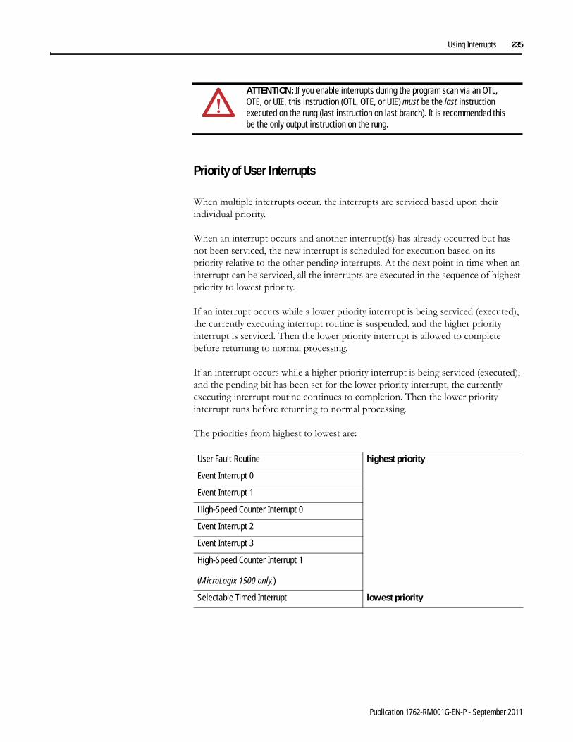
Using Interrupts 235
Priority of User Interrupts
When multiple interrupts occur, the interrupts are serviced based upon their individual priority.
When an interrupt occurs and another interrupt(s) has already occurred but has not been serviced, the new interrupt is scheduled for execution based on its priority relative to the other pending interrupts. At the next point in time when an interrupt can be serviced, all the interrupts are executed in the sequence of highest priority to lowest priority.
If an interrupt occurs while a lower priority interrupt is being serviced (executed), the currently executing interrupt routine is suspended, and the higher priority interrupt is serviced. Then the lower priority interrupt is allowed to complete before returning to normal processing.
If an interrupt occurs while a higher priority interrupt is being serviced (executed), and the pending bit has been set for the lower priority interrupt, the currently executing interrupt routine continues to completion. Then the lower priority interrupt runs before returning to normal processing.
The priorities from highest to lowest are:
ATTENTION: If you enable interrupts during the program scan via an OTL, OTE, or UIE, this instruction (OTL, OTE, or UIE) must be the last instruction executed on the rung (last instruction on last branch). It is recommended this be the only output instruction on the rung.
User Fault Routine highest priority
Event Interrupt 0
Event Interrupt 1
High-Speed Counter Interrupt 0
Event Interrupt 2
Event Interrupt 3
High-Speed Counter Interrupt 1
(MicroLogix 1500 only.)
Selectable Timed Interrupt lowest priority
Publication 1762-RM001G-EN-P - September 2011
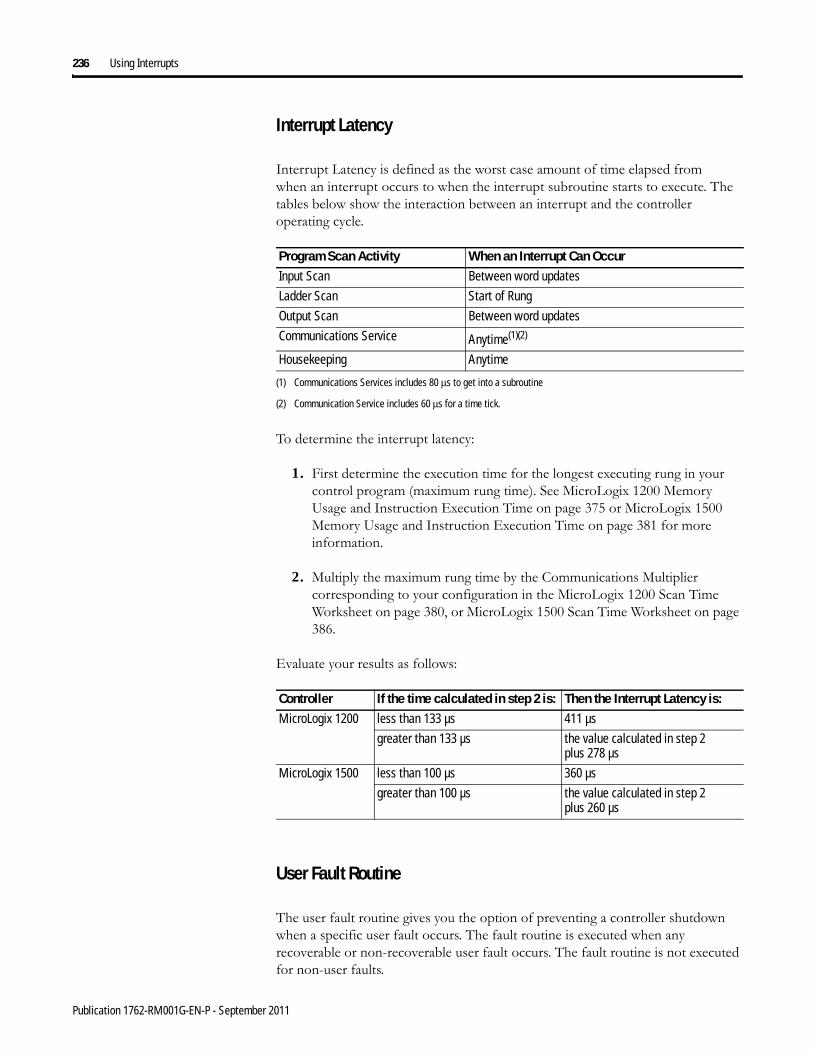
236 Using Interrupts
Interrupt Latency
Interrupt Latency is defined as the worst case amount of time elapsed from when an interrupt occurs to when the interrupt subroutine starts to execute. The tables below show the interaction between an interrupt and the controller operating cycle.
To determine the interrupt latency:
1. First determine the execution time for the longest executing rung in your control program (maximum rung time). See MicroLogix 1200 Memory Usage and Instruction Execution Time on page 375 or MicroLogix 1500 Memory Usage and Instruction Execution Time on page 381 for more information.
2. Multiply the maximum rung time by the Communications Multiplier corresponding to your configuration in the MicroLogix 1200 Scan Time Worksheet on page 380, or MicroLogix 1500 Scan Time Worksheet on page 386.
Evaluate your results as follows:
User Fault Routine
The user fault routine gives you the option of preventing a controller shutdown when a specific user fault occurs. The fault routine is executed when any recoverable or non-recoverable user fault occurs. The fault routine is not executed for non-user faults.
Program Scan Activity When an Interrupt Can OccurInput Scan Between word updates
Ladder Scan Start of Rung
Output Scan Between word updates
Communications Service Anytime(1)(2)
(1) Communications Services includes 80 μs to get into a subroutine
(2) Communication Service includes 60 μs for a time tick.
Housekeeping Anytime
Controller If the time calculated in step 2 is: Then the Interrupt Latency is:MicroLogix 1200 less than 133 µs 411 µs
greater than 133 µs the value calculated in step 2 plus 278 µs
MicroLogix 1500 less than 100 µs 360 µs
greater than 100 µs the value calculated in step 2 plus 260 µs
Publication 1762-RM001G-EN-P - September 2011

Using Interrupts 237
Faults are classified as recoverable, non-recoverable, and non-user faults. A complete list of faults is shown in Fault Messages and Error Codes on page 413. The basic types of faults are described below:
Status File Data Saved
The Arithmetic Flags (Status File word S:0) are saved on entry to the user fault subroutine and re-written upon exiting the subroutine.
Creating a User Fault Subroutine
To use the user fault subroutine:
1. Create a subroutine file. Program Files 3 to 255 can be used.
2. Enter the file number in word S:29 of the status file.
Controller Operation
The occurrence of recoverable or non-recoverable faults causes the controller to read S:29 and execute the subroutine number identified by S:29. If the fault is recoverable, the routine can be used to correct the problem and clear the fault bit S:1/13. The controller then continues in its current executing mode. The routine does not execute for non-user faults.
User Interrupt Instructions
Recoverable Non-Recoverable Non-User FaultRecoverable Faults are caused by the user and may be recovered from by executing logic in the user fault routine. The user can attempt to clear the Major Error Halted bit, S:1/13.
Note: You may initiate a MSG instruction from the controller to another device to identify the fault condition of the controller.
Non-Recoverable Faults are caused by the user, and cannot be recovered from. The user fault routine executes when this type of fault occurs. However, the fault cannot be cleared.
Note: You may initiate a MSG instruction to another device to identify the fault condition of the controller.
Non-User Faults are caused by various conditions that cease ladder program execution. The user fault routine does not execute when this type of fault occurs.
Instruction Used To: PageINT - Interrupt Subroutine Use this instruction to identify a program file as an
interrupt subroutine (INT label) versus a regular subroutine (SBR label). This should be the first instruction in your interrupt subroutine.
238
Publication 1762-RM001G-EN-P - September 2011

238 Using Interrupts
INT - Interrupt Subroutine
Instruction Type: input
The INT instruction is used as a label to identify a user interrupt service routine (ISR). This instruction is placed as the first instruction on a rung and is always evaluated as true. Use of the INT instruction is optional.
STS - Selectable Timed Start
Instruction Type: output
The STS instruction can be used to start and stop the STI function or to change the time interval between STI user interrupts. The STI instruction has one operand:
• Time - This is the amount of time (in milliseconds) which must expire prior to executing the selectable timed user interrupt. A value of zero disables the STI function. The time range is from 0 to 65,535 milliseconds.
The STS instruction applies the specified set point to the STI function as follows:
STS - Selectable Timed Start
Use the STS (Selectable Timed Interrupt Start) instruction to the start the STI timer from the control program, rather than starting automatically.
238
UID - User Interrupt Disable Use the User Interrupt Disable (UID) and the User Interrupt Enable (UIE) instructions to create zones in which I/O interrupts cannot occur.
239
UIE - User Interrupt Enable 240
UIF - User Interrupt Flush Use the UIF instruction to remove selected pending interrupts from the system.
241
Instruction Used To: Page
INTI/O Interrupt
INTExecution Time for the INT Instruction
Controller When Rung Is:True False
MicroLogix 1200 1.0 μs 1.0 μs
MicroLogix 1500 1.0 μs 1.0 μs
STSSelectable Timed StartTime 1
STSExecution Time for the STS Instruction
Controller When Rung Is:True False
MicroLogix 1200 57.5 μs 0.0 μsMicroLogix 1500 50.7 μs 0.0 μs
Publication 1762-RM001G-EN-P - September 2011

Using Interrupts 239
• If a zero set point is specified, the STI is disabled and STI:0/TIE is cleared (0).
• If the STI is disabled (not timing) and a value greater than 0 is entered into the set point, the STI starts timing to the new set point and STI:0/TIE is set (1).
• If the STI is currently timing and the set point is changed, the new setting takes effect immediately and the STI continues to time until it reaches the new set point.
Note that if the new setting is less than the current accumulated time, the STI times-out immediately. For example, if the STI has been timing for 15 microseconds, and the STI set point is changed from 20 microseconds to 10 microseconds, an STI user interrupt occurs at the next start-of-rung.
Addressing Modes and File Types can be used as shown below:
UID - User Interrupt Disable
Instruction Type: output
The UID instruction is used to disable selected user interrupts. The table below shows the types of interrupts with their corresponding disable bits:
STS Instruction Valid Addressing Modes and File TypesFor definitions of the terms used in this table see Using the Instruction Descriptions on page 82.
Parameter
Data Files Function Files
CS -
Com
ms
IOS
- I/O
DLS
- D
ata
Log
Address(1) Mode
Address Level
O I S B T, C
, R
N F ST L MG
, PD
PLS
RTC
HSC
PTO
, PW
M
STI
EII
BHI
MM
I
DAT
TPI
Imm
edia
te
Dir
ect
Indi
rect
Elem
ent
Bit
Wor
d
Long
Wor
d
Time • • • • • • • • •
(1) See Important note about indirect addressing.
IMPORTANT You cannot use indirect addressing with: S, ST, MG, PD, RTC, HSC, PTO, PWM, STI, EII, BHI, MMI, DAT, TPI, CS, IOS, and DLS files.
UIDUser Interrupt DisableInterrupt Types 5
UIDExecution Time for the UID Instruction
Controller When Rung Is:True False
MicroLogix 1200 0.8 μs 0.0 μsMicroLogix 1500 0.8 μs 0.0 μs
Types of Interrupts Disabled by the UID Instruction
Interrupt Element Decimal Value
Corresponding Bit
EII - Event Input Interrupts Event 0 64 bit 6
Publication 1762-RM001G-EN-P - September 2011

240 Using Interrupts
To disable interrupt(s):
1. Select which interrupts you want to disable.
2. Find the Decimal Value for the interrupt(s) you selected.
3. Add the Decimal Values if you selected more than one type of interrupt.
4. Enter the sum into the UID instruction.
For example, to disable EII Event 1 and EII Event 3:
EII Event 1 = 32, EII Event 3 = 4
32 + 4 = 36 (enter this value)
UIE - User Interrupt Enable
Instruction Type: output
The UIE instruction is used to enable selected user interrupts. The table below shows the types of interrupts with their corresponding enable bits:
EII - Event Input Interrupts Event 1 32 bit 5HSC - High-Speed Counter HSC0 16 bit 4EII - Event Input Interrupts Event 2 8 bit 3EII - Event Input Interrupts Event 3 4 bit 2
HSC - High-Speed Counter(1) HSC1 2 bit 1
STI - Selectable Timed Interrupts STI 1 bit 0Note: Bits 7 to 15 must be set to zero.
(1) The MicroLogix 1200 has one HSC Interrupt, HSC0. The MicroLogix 1500 has two, HSC0 and HSC1.
Types of Interrupts Disabled by the UID Instruction
Interrupt Element Decimal Value
Corresponding Bit
UIEUser Interrupt EnableInterrupt Types 4
UIEExecution Time for the UIE Instruction
Controller When Rung Is:True False
MicroLogix 1200 0.8 μs 0.0 μs
MicroLogix 1500 0.8 μs 0.0 μs
Types of Interrupts Disabled by the UIE Instruction
Interrupt Element Decimal Value
Corresponding Bit
EII - Event Input Interrupts Event 0 64 bit 6
Publication 1762-RM001G-EN-P - September 2011

Using Interrupts 241
To enable interrupt(s):
1. Select which interrupts you want to enable.
2. Find the Decimal Value for the interrupt(s) you selected.
3. Add the Decimal Values if you selected more than one type of interrupt.
4. Enter the sum into the UIE instruction.
For example, to enable EII Event 1 and EII Event 3:
EII Event 1 = 32, EII Event 3 = 432 + 4 = 36 (enter this value)
UIF - User Interrupt Flush
Instruction Type: output
The UIF instruction is used to flush (remove pending interrupts from the system) selected user interrupts. The table below shows the types of interrupts with their
EII - Event Input Interrupts Event 1 32 bit 5
HSC - High-Speed Counter HSC0 16 bit 4
EII - Event Input Interrupts Event 2 8 bit 3
EII - Event Input Interrupts Event 3 4 bit 2
HSC - High-Speed Counter(1) HSC1 2 bit 1
STI - Selectable Timed Interrupts STI 1 bit 0
Note: Bits 7 to 15 must be set to zero.
(1) The MicroLogix 1200 has one HSC Interrupt, HSC0. The MicroLogix 1500 has two, HSC0 and HSC1.
ATTENTION: If you enable interrupts during the program scan via an OTL, OTE, or UIE, this instruction must be the last instruction executed on the rung (last instruction on last branch). It is recommended this be the only output instruction on the rung.
Types of Interrupts Disabled by the UIE Instruction
Interrupt Element Decimal Value
Corresponding Bit
UIFUser Interrupt FlushInterrupt Types 1
UIFExecution Time for the UIF Instruction
Controller When Rung Is:True False
MicroLogix 1200 12.3 μs 0.0 μs
MicroLogix 1500 10.6 μs 0.0 μs
Publication 1762-RM001G-EN-P - September 2011
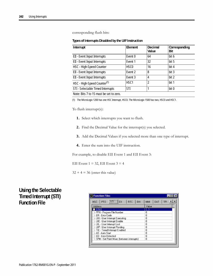
242 Using Interrupts
corresponding flush bits:
To flush interrupt(s):
1. Select which interrupts you want to flush.
2. Find the Decimal Value for the interrupt(s) you selected.
3. Add the Decimal Values if you selected more than one type of interrupt.
4. Enter the sum into the UIF instruction.
For example, to disable EII Event 1 and EII Event 3:
EII Event 1 = 32, EII Event 3 = 4
32 + 4 = 36 (enter this value)
Using the Selectable Timed Interrupt (STI) Function File
Types of Interrupts Disabled by the UIF Instruction
Interrupt Element Decimal Value
Corresponding Bit
EII - Event Input Interrupts Event 0 64 bit 6
EII - Event Input Interrupts Event 1 32 bit 5
HSC - High-Speed Counter HSC0 16 bit 4
EII - Event Input Interrupts Event 2 8 bit 3
EII - Event Input Interrupts Event 3 4 bit 2
HSC - High-Speed Counter(1)
(1) The MicroLogix 1200 has one HSC Interrupt, HSC0. The MicroLogix 1500 has two, HSC0 and HSC1.
HSC1 2 bit 1
STI - Selectable Timed Interrupts STI 1 bit 0
Note: Bits 7 to 15 must be set to zero.
Publication 1762-RM001G-EN-P - September 2011

Using Interrupts 243
The Selectable Timed Interrupt (STI) provides a mechanism to solve time critical control requirements. The STI is a trigger mechanism that allows you to scan or solve control program logic that is time sensitive.
Example of where you would use the STI are:
• PID type applications, where a calculation must be performed at a specific time interval.
• A motion application, where the motion instruction (PTO) needs to be scanned at a specific rate to guarantee a consistent acceleration/deceleration profile.
• A block of logic that needs to be scanned more often.
How an STI is used is typically driven by the demands/requirements of the application. It operates using the following sequence:
1. The user selects a time interval.
2. When a valid interval is set and the STI is properly configured, the controller monitors the STI value.
3. When the time period has elapsed, the controller’s normal operation is interrupted.
4. The controller then scans the logic in the STI program file.
5. When the STI file scan is completed, the controller returns to where it was prior to the interrupt and continues normal operation.
Selectable Time Interrupt (STI) Function File Sub-Elements Summary
Selectable Timed Interrupt Function File (STI:0)
Sub-Element Description Address Data Format Type User Program Access
For More Information
PFN - Program File Number STI:0.PFN word (INT) control read only 244
ER - Error Code STI:0.ER word (INT) status read only 244
UIX - User Interrupt Executing STI:0/UIX binary (bit) status read only 244
UIE - User Interrupt Enable STI:0/UIE binary (bit) control read/write 245
UIL - User Interrupt Lost STI:0/UIL binary (bit) status read/write 245
UIP - User Interrupt Pending STI:0/UIP binary (bit) status read only 245
TIE - Timed Interrupt Enabled STI:0/TIE binary (bit) control read/write 246
AS - Auto Start STI:0/AS binary (bit) control read only 246
ED - Error Detected STI:0/ED binary (bit) status read only 246
SPM - Set Point Msec STI:0.SPM word (INT) control read/write 246
Publication 1762-RM001G-EN-P - September 2011

244 Using Interrupts
STI Function File Sub-Elements
STI Program File Number (PFN)
The PFN (Program File Number) variable defines which subroutine is called (executed) when the timed interrupt times out. A valid subroutine file is any program file (3 to 255).
The subroutine file identified in the PFN variable is not a special file within the controller; it is programmed and operates the same as any other program file. From the control program perspective it is unique, in that it is automatically scanned based on the STI set point.
STI Error Code (ER)
Error codes detected by the STI sub-system are displayed in this register. The table below explains the error codes.
STI User Interrupt Executing (UIX)
The UIX (User Interrupt Executing) bit is set whenever the STI mechanism completes timing and the controller is scanning the STI PFN. The UIX bit is cleared when the controller completes processing the STI subroutine.
The STI UIX bit can be used in the control program as conditional logic to detect if an STI interrupt is executing.
Sub-Element Description Address Data Format Type User Program Access
PFN - Program File Number STI:0.PFN word (INT) control read only
Sub-Element Description Address Data Format Type User Program Access
ER - Error Code STI:0.ER word (INT) status read only
STI Error Code
Error Code
Recoverable Fault (Controller)
Description
1 Invalid Program File Number
Program file number is less than 3, greater than 255, or does not exist.
Sub-Element Description Address Data Format Type User Program Access
UIX - User Interrupt Executing STI:0/UIX binary (bit) status read only
Publication 1762-RM001G-EN-P - September 2011

Using Interrupts 245
STI User Interrupt Enable (UIE)
The UIE (User Interrupt Enable) bit is used to enable or disable STI subroutine processing. This bit must be set if you want the controller to process the STI subroutine at the configured time interval.
If you need to restrict when the STI subroutine is processed, clear the UIE bit. An example of when this is important is if a series of math calculations need to be processed without interruption. Before the calculations take place, clear the UIE bit. After the calculations are complete, set the UIE bit and STI subroutine processing resumes.
STI User Interrupt Lost (UIL)
The UIL (User Interrupt Lost) is a status flag that indicates an interrupt was lost. The controller can process 1 active and maintain up to 2 pending user interrupt conditions before it sets the lost bit.
This bit is set by the controller. It is up to the control program to utilize, track if necessary, and clear the lost condition.
STI User Interrupt Pending (UIP)
The UIP (User Interrupt Pending) is a status flag that represents an interrupt is pending. This status bit can be monitored or used for logic purposes in the control program if you need to determine when a subroutine cannot execute immediately.
This bit is automatically set and cleared by the controller. The controller can process 1 active and maintain up to 2 pending user interrupt conditions before it sets the lost bit.
Sub-Element Description Address Data Format Type User Program Access
UIE - User Interrupt Enable STI:0/UIE binary (bit) control read/write
Sub-Element Description Address Data Format Type User Program Access
UIL - User Interrupt Lost STI:0/UIL binary (bit) status read/write
Sub-Element Description Address Data Format Type User Program Access
UIP - User Interrupt Pending STI:0/UIP binary (bit) status read only
Publication 1762-RM001G-EN-P - September 2011
246 Using Interrupts
STI Timed Interrupt Enabled (TIE)
The TIE (Timed Interrupt Enabled) control bit is used to enable or disable the timed interrupt mechanism. When set (1), timing is enabled, when clear (0) timing is disabled. If this bit is cleared (disabled) while the timer is running, the accumulated value is cleared (0). If the bit is then set (1), timing starts.
This bit is controlled by the user program and retains its value through a power cycle.
STI Auto Start (AS)
The AS (Auto Start) is a control bit that can be used in the control program. The auto start bit is configured with the programming device and stored as part of the user program. The auto start bit automatically sets the STI Timed Interrupt Enable (TIE) bit when the controller enters any executing mode.
STI Error Detected (ED)
The ED (Error Detected) flag is a status bit that can be used by the control program to detect if an error is present in the STI sub-system. The most common type of error that this bit represents is a configuration error. When this bit is set, the user should look at the error code in parameter STI:0.ER
This bit is automatically set and cleared by the controller.
STI Set Point Milliseconds Between Interrupts (SPM)
When the controller transitions to an executing mode, the SPM (set point in milliseconds) value is loaded into the STI. If the STI is configured correctly, and
Sub-Element Description Address Data Format Type User Program Access
TIE - Timed Interrupt Enabled STI:0/TIE binary (bit) control read/write
Sub-Element Description Address Data Format Type User Program Access
AS - Auto Start STI:0/AS binary (bit) control read only
Sub-Element Description Address Data Format Type User Program Access
ED - Error Detected STI:0/ED binary (bit) status read only
Sub-Element Description
Address Data Format Range Type User Program Access
SPM - Set Point Msec
STI:0.SPM word (INT) 0 to 65,535
control read/write
Publication 1762-RM001G-EN-P - September 2011

Using Interrupts 247
enabled, the program file identified in the STI variable PFN is scanned at this interval. This value can be changed from the control program by using the STS instruction.
Using the Event Input Interrupt (EII) Function File
The EII (event input interrupt) is a feature that allows the user to scan a specific program file (subroutine) when an input condition is detected from a field device.
Within the function file section of RSLogix 500, the user sees an EII folder. Within the folder are four EII elements. Each of these elements (EII:0, EII:1, EII:2, and EII:3) are identical; this explanation uses EII:0 as shown below.
Each EII can be configured to monitor any one of the first eight inputs (I1:0.0/0 to I1:0.0/7). Each EII can be configured to detect rising edge or falling edge input signals. When the configured input signal is detected at the input terminal, the controller immediately scans the configured subroutine.
Event Input Interrupt (EII) Function File Sub-Elements Summary
TIP The minimum value cannot be less than the time required to scan the STI program file (STI:0.PFN) plus the Interrupt Latency.
Event Input Interrupt Function File (EII:0)
Sub-Element Description Address Data Format Type User Program Access
For More Information
PFN - Program File Number EII:0.PFN word (INT) control read only 248
ER - Error Code EII:0.ER word (INT) status read only 248
UIX - User Interrupt Executing EII:0/UIX binary (bit) status read only 249
UIE - User Interrupt Enable EII:0/UIE binary (bit) control read/write 249
UIL - User Interrupt Lost EII:0/UIL binary (bit) status read/write 249
UIP - User Interrupt Pending EII:0/UIP binary (bit) status read only 250
Publication 1762-RM001G-EN-P - September 2011
248 Using Interrupts
EII Function File Sub-Elements
EII Program File Number (PFN)
PFN (Program File Number) defines which subroutine is called (executed) when the input terminal assigned to EII:0 detects a signal. A valid subroutine file is any program file (3 to 255).
The subroutine file identified in the PFN variable is not a special file within the controller. It is programmed and operated the same as any other program file. From the control program perspective it is unique, in that it is automatically scanned based on the configuration of the EII.
EII Error Code (ER)
Any ER (Error Code) detected by the EII sub-system is displayed in this register. The table below explains the error codes.
EIE - Event Interrupt Enabled EII:0/EIE binary (bit) control read/write 250
AS - Auto Start EII:0/AS binary (bit) control read only 250
ED - Error Detected EII:0/ED binary (bit) status read only 251
ES - Edge Select EII:0/ES binary (bit) control read only 251
IS - Input Select EII:0.IS word (INT) control read only 251
Event Input Interrupt Function File (EII:0)
Sub-Element Description Address Data Format Type User Program Access
For More Information
Sub-Element Description Address Data Format Type User Program Access
PFN - Program File Number EII:0.PFN word (INT) control read only
Sub-Element Description Address Data Format Type User Program Access
ER - Error Code EII:0.ER word (INT) status read only
EII Error Codes
Error Code
Recoverable Fault (Controller)
Description
1 Invalid Program File Number
Program file number is less than 3, greater than 255, or does not exist
2 Invalid Input Selection Valid numbers must be 0, 1, 2, 3, 4, 5, 6, or 7.3 Input Selection Overlap EIIs cannot share inputs. Each EII must have a unique
input.
Publication 1762-RM001G-EN-P - September 2011

Using Interrupts 249
EII User Interrupt Executing (UIX)
The UIX (User Interrupt Executing) bit is set whenever the EII mechanism detects a valid input and the controller is scanning the PFN. The EII mechanism clears the UIX bit when the controller completes its processing of the EII subroutine.
The EII UIX bit can be used in the control program as conditional logic to detect if an EII interrupt is executing.
EII User Interrupt Enable (UIE)
The UIE (User Interrupt Enable) bit is used to enable or disable EII subroutine processing. This bit must be set if you want the controller to process the EII subroutine when an EII event occurs.
If you need to restrict when the EII subroutine is processed, clear the UIE bit. An example of when this is important is if a series of math calculations need to be processed without interruption. Before the calculations take place, clear the UIE bit. After the calculations are complete, set the UIE bit and EII subroutine processing resumes.
EII User Interrupt Lost (UIL)
UIL (User Interrupt Lost) is a status flag that represents an interrupt has been lost. The controller can process 1 active and maintain up to 2 pending user interrupt conditions before it sets the lost bit.
This bit is set by the controller. It is up to the control program to utilize, track, and clear the lost condition.
Sub-Element Description Address Data Format Type User Program Access
UIX - User Interrupt Executing EII:0/UIX binary (bit) status read only
Sub-Element Description Address Data Format Type User Program Access
UIE - User Interrupt Enable EII:0/UIE binary (bit) control read/write
Sub-Element Description Address Data Format Type User Program Access
UIL - User Interrupt Lost EII:0/UIL binary (bit) status read/write
Publication 1762-RM001G-EN-P - September 2011
250 Using Interrupts
EII User Interrupt Pending (UIP)
UIP (User Interrupt Pending) is a status flag that represents an interrupt is pending. This status bit can be monitored, or used for logic purposes, in the control program if you need to determine when a subroutine cannot execute immediately.
This bit is automatically set and cleared by the controller. The controller can process 1 active and maintain up to 2 pending user interrupt conditions before it sets the pending bit.
EII Event Interrupt Enable (EIE)
EIE (Event Interrupt Enabled) allows the event interrupt function to be enabled or disabled from the control program. When set (1), the function is enabled, when cleared (0, default) the function is disabled.
This bit is controlled by the user program and retains its value through a power cycle.
EII Auto Start (AS)
AS (Auto Start) is a control bit that can be used in the control program. The auto start bit is configured with the programming device and stored as part of the user program. The auto start bit automatically sets the EII Event Interrupt Enable (EIE) bit when the controller enters any executing mode.
Sub-Element Description Address Data Format Type User Program Access
UIP - User Interrupt Pending EII:0/UIP binary (bit) status read only
Sub-Element Description Address Data Format Type User Program Access
EIE - Event Interrupt Enabled EII:0/EIE binary (bit) control read/write
Sub-Element Description Address Data Format Type User Program Access
AS - Auto Start EII:0/AS binary (bit) control read only
Publication 1762-RM001G-EN-P - September 2011

Using Interrupts 251
EII Error Detected (ED)
The ED (Error Detected) flag is a status bit that can be used by the control program to detect if an error is present in the EII sub-system. The most common type of error that this bit represents is a configuration error. When this bit is set, look at the specific error code in parameter EII:0.ER
This bit is automatically set and cleared by the controller.
EII Edge Select (ES)
The ES (Edge Select) bit selects the type of trigger that causes an Event Interrupt. This bit allows the EII to be configured for rising edge (off-to-on, 0-to-1) or falling edge (on-to-off, 1-to-0) signal detection. This selection is based on the type of field device that is connected to the controller.
The default condition is 1, which configures the EII for rising edge operation.
EII Input Select (IS)
The IS (Input Select) parameter is used to configure each EII to a specific input on the controller. Valid inputs are 0 to 7, which correspond to I1:0.0/0 to I1:0.0/7.
This parameter is configured with the programming device and cannot be changed from the control program.
Sub-Element Description Address Data Format Type User Program Access
ED - Error Detected EII:0/ED binary (bit) status read only
Sub-Element Description Address Data Format Type User Program Access
ES - Edge Select EII:0/ES binary (bit) control read only
Sub-Element Description Address Data Format Type User Program Access
IS - Input Select EII:0.IS word (INT) control read only
Publication 1762-RM001G-EN-P - September 2011

252 Using Interrupts
Notes:
Publication 1762-RM001G-EN-P - September 2011
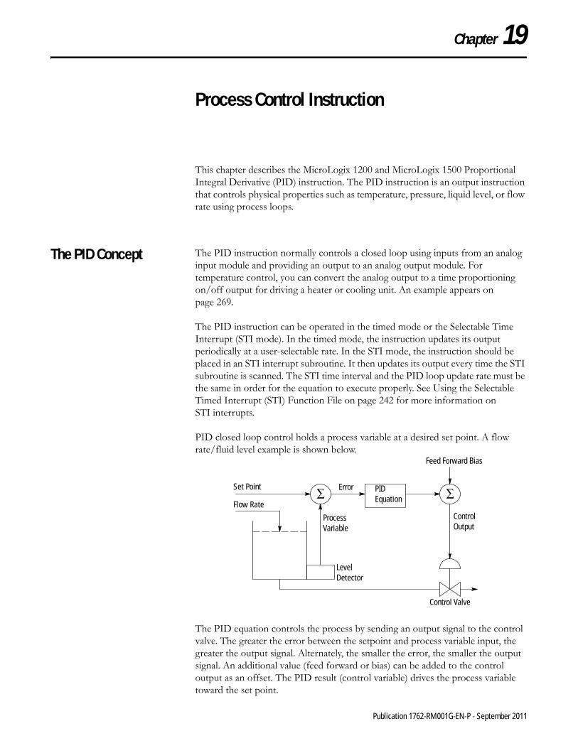
Chapter 19
Process Control Instruction
This chapter describes the MicroLogix 1200 and MicroLogix 1500 Proportional Integral Derivative (PID) instruction. The PID instruction is an output instruction that controls physical properties such as temperature, pressure, liquid level, or flow rate using process loops.
The PID Concept The PID instruction normally controls a closed loop using inputs from an analog input module and providing an output to an analog output module. For temperature control, you can convert the analog output to a time proportioning on/off output for driving a heater or cooling unit. An example appears on page 269.
The PID instruction can be operated in the timed mode or the Selectable Time Interrupt (STI mode). In the timed mode, the instruction updates its output periodically at a user-selectable rate. In the STI mode, the instruction should be placed in an STI interrupt subroutine. It then updates its output every time the STI subroutine is scanned. The STI time interval and the PID loop update rate must be the same in order for the equation to execute properly. See Using the Selectable Timed Interrupt (STI) Function File on page 242 for more information on STI interrupts.
PID closed loop control holds a process variable at a desired set point. A flow rate/fluid level example is shown below.
The PID equation controls the process by sending an output signal to the control valve. The greater the error between the setpoint and process variable input, the greater the output signal. Alternately, the smaller the error, the smaller the output signal. An additional value (feed forward or bias) can be added to the control output as an offset. The PID result (control variable) drives the process variable toward the set point.
∑ ∑Set Point
Flow Rate
Error
Control Valve
PIDEquation
Process Variable
Level Detector
Control Output
Feed Forward Bias
253 Publication 1762-RM001G-EN-P - September 2011

254 Process Control Instruction
The PID Equation The PID instruction uses the following algorithm:
Standard equation with dependent gains:
Standard Gains constants are:
The derivative term (rate) provides smoothing by means of a low-pass filter. The cut-off frequency of the filter is 16 times greater than the corner frequency of the derivative term.
PD Data FileThe PID instruction implemented by the MicroLogix 1200 and 1500 controllers is virtually identical in function to the PID implementation used by the Allen-Bradley SLC 5/03 and higher processors. Minor differences primarily involve enhancements to terminology. The major difference is that the PID instruction now has its own data file. In the SLC family of processors, the PID instruction operated as a block of registers within an integer file. The Micrologix 1200 and 1500 PID instruction utilizes a PD data file.
You can create a PD data file by creating a new data file and classifying it as a PD file type. RSLogix automatically creates a new PD file or a PD sub-element whenever a PID instruction is programmed on a rung. The PD file then appears in the list of Data Files as shown in the illustration.
Each PD data file has a maximum of 255 elements and each PID instruction requires a unique PD element. Each PD element is composed of 20 sub-elements, which include bit, integer and long integer data. All of the examples in this chapter use PD file 10 sub-element 0.
Term Range (Low to High) ReferenceController Gain KC 0.01 to 327.67 (dimensionless)(1)
(1) Applies to MicroLogix 1200 and 1500 PID range when Reset and Gain Range (RG) bit is set to 1. For more information on reset and gain, see PLC 5 Gain Range (RG) on page 265.
Proportional
Reset Term 1/TI 327.67 to 0.01 (minutes per repeat)(1) Integral
Rate Term TD 0.01 to 327.67 (minutes)(1) Derivative
Output KC E( ) 1TI----- E( ) td∫ TD
d PV( )dt
---------------⋅+ + bias+=
PD file created by RSLogix 500.
Publication 1762-RM001G-EN-P - September 2011

Process Control Instruction 255
PID - Proportional Integral Derivative
Instruction Type: output
It is recommended that you place the PID instruction on a rung without any conditional logic. If conditional logic exists, the Control Variable output remains at its last value, and the CVP CV% term and integral term are both cleared when the rung is false.
The example below shows a PID instruction on a rung with RSLogix 500 programming software.
When programming, the setup screen provides access to the PID instruction configuration parameters. The illustration below shows the RSLogix 500 setup screen.
PIDPIDPID File PD8:0Process Variable N7:0Control Variable N7:1
Setup Screen
PIDExecution Time for the PID Instruction
Controller When Rung Is:True False
MicroLogix 1200 295.8 μs 11.0 μsMicroLogix 1500 251.8 μs 8.9 μs
TIP In order to stop and restart the PID instruction, you need to create a false-to-true rung transition.
0047B3:0
0
PIDPIDPID File PD8:0Process Variable N7:0Control Variable N7:1
Setup Screen
PID
Publication 1762-RM001G-EN-P - September 2011

256 Process Control Instruction
Input Parameters The table below shows the input parameter addresses, data formats, and types of user program access. See the indicated pages for descriptions of each parameter.
Setpoint (SPS)
The SPS (Setpoint) is the desired control point of the process variable.
Process Variable (PV)
The PV (Process Variable) is the analog input variable.
Input Parameter Descriptions Address Data Format Range Type User Program Access
For More Information
SPS - Setpoint PD10:0.SPS word (INT) 0 to 16383(1) control read/write 256
PV - Process Variable user defined word (INT) 0 to 16383 control read/write 256
MAXS - Setpoint Maximum PD10:0.MAXS word (INT) -32,768 to +32,767 control read/write 257
MINS - Setpoint Minimum PD10:0.MINS word (INT) -32,768 to +32,767 control read/write 257
OSP - Old Setpoint Value PD10:0.OSP word (INT) -32,768 to +32,767 status read only 257
OL - Output Limit PD10:0/OL binary 1 = enabled0 = disabled
control read/write 258
CVH - Control Variable High Limit
PD10:0.CVH word (INT) 0 to 100% control read/write 258
CVL - Control Variable Low Limit PD10:0.CVL word (INT) 0 to 100% control read/write 258
(1) The range listed in the table is for when scaling is not enabled. With scaling, the range is from minimum scaled (MINS) to maximum scaled (MAXS).
Input Parameter Descriptions
Address Data Format Range Type User Program Access
SPS - Setpoint PD10:0.SPS word (INT) 0 to 16383(1)
(1) The range listed in the table is for when scaling is not enabled. With scaling, the range is from minimum scaled (MINS) to maximum scaled (MAXS).
control read/write
Input Parameter Descriptions
Address Data Format Range Type User Program Access
PV - Process Variable
user defined word (INT) 0 to 16383 control read/write
Publication 1762-RM001G-EN-P - September 2011

Process Control Instruction 257
Setpoint MAX (MAXS)
If the SPV is read in engineering units, then the MAXS (Setpoint Maximum) parameter corresponds to the value of the setpoint in engineering units when the control input is at its maximum value.
Setpoint MIN (MINS)
If the SPV is read in engineering units, then the MINS (Setpoint Minimum) parameter corresponds to the value of the setpoint in engineering units when the control input is at its minimum value.
Scaled errors greater than +32767 or less than -32768 cannot be represented. If the scaled error is greater than +32767, it is represented as +32767. If the scaled error is less than -32768, it is represented as -32768.
Old Setpoint Value (OSP)
The OSP (Old Setpoint Value) is substituted for the current setpoint, if the current setpoint goes out of range of the setpoint scaling (limiting) parameters.
Input Parameter Descriptions
Address Data Format
Range Type User Program Access
MAXS - Setpoint Maximum
PD10:0.MAXS word (INT)
-32,768 to +32,767 control read/write
Input Parameter Descriptions
Address Data Format
Range Type User Program Access
MINS - Setpoint Minimum
PD10:0.MINS word (INT)
-32,768 to +32,767 control read/write
TIP MinS - MaxS scaling allows you to work in engineering units. The deadband, error, and SPV are also displayed in engineering units. The process variable, PV, must be within the range of 0 to 16383. Use of MinS - MaxS does not minimize PID PV resolution.
Input Parameter Descriptions
Address Data Format
Range Type User Program Access
OSP - Old Setpoint Value
PD10:0.OSP word (INT)
-32,768 to +32,767 status read only
Publication 1762-RM001G-EN-P - September 2011

258 Process Control Instruction
Output Limit (OL)
An enabled (1) value enables output limiting to the values defined in PD10:0.CVH (Control Variable High) and PD10.0.CVL (Control Variable Low).
A disabled (0) value disables OL (Output Limiting).
Control Variable High Limit (CVH)
When the output limit bit (PD10:0/OL) is enabled (1), the CVH (Control Value High) you enter is the maximum output (in percent) that the control variable attains. If the calculated CV exceeds the CVH, the CV is set (overridden) to the CVH value you entered and the upper limit alarm bit (UL) is set.
When the output limit bit (PD10:0/OL) is disabled (0), the CVH value you enter determines when the upper limit alarm bit (UL) is set.
If CV exceeds the maximum value, the output is not overridden and the upper limit alarm bit (UL) is set.
Control Variable Low Limit (CVL)
When the output limit bit (PD10:0/OL) is enabled (1), the CVL (Control Value Low) you enter is the minimum output (in percent) that the Control Variable attains. If the calculated CV is below the minimum value, the CV is set (overridden) to the CVL value you entered and the lower limit alarm bit (LL) is set.
Output Parameter Descriptions
Address Data Format
Range Type User Program Access
OL - Output Limit PD10:0/OL binary 1 = enabled0 = disabled
control read/write
Output Parameter Descriptions
Address Data Format Range Type User Program Access
CVH - Control Variable High Limit
PD10:0.CVH word (INT) 0 to 100% control read/write
Output Parameter Descriptions
Address Data Format
Range Type User Program Access
CVL - Control Variable Low Limit
PD10:0.CVL word (INT)
0 to 100% control read/write
Publication 1762-RM001G-EN-P - September 2011
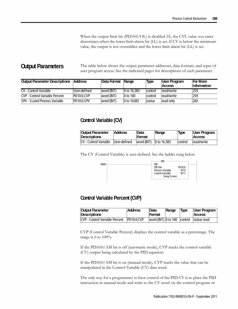
Process Control Instruction 259
When the output limit bit (PD10:0/OL) is disabled (0), the CVL value you enter determines when the lower limit alarm bit (LL) is set. If CV is below the minimum value, the output is not overridden and the lower limit alarm bit (LL) is set.
Output Parameters The table below shows the output parameter addresses, data formats, and types of user program access. See the indicated pages for descriptions of each parameter.
Control Variable (CV)
The CV (Control Variable) is user-defined. See the ladder rung below.
Control Variable Percent (CVP)
CVP (Control Variable Percent) displays the control variable as a percentage. The range is 0 to 100%.
If the PD10:0/AM bit is off (automatic mode), CVP tracks the control variable (CV) output being calculated by the PID equation.
If the PD10:0/AM bit is on (manual mode), CVP tracks the value that can be manipulated in the Control Variable (CV) data word.
The only way for a programmer to have control of the PID CV is to place the PID instruction in manual mode and write to the CV word via the control program or
Output Parameter Descriptions Address Data Format Range Type User Program Access
For More Information
CV - Control Variable User-defined word (INT) 0 to 16,383 control read/write 259CVP - Control Variable Percent PD10:0.CVP word (INT) 0 to 100 control read/write 259SPV - Scaled Process Variable PD10:0.SPV word (INT) 0 to 16383 status read only 260
Output Parameter Descriptions
Address Data Format
Range Type User Program Access
CV - Control Variable User-defined word (INT) 0 to 16,383 control read/write
Output Parameter Descriptions
Address Data Format
Range Type User Program Access
CVP - Control Variable Percent PD10:0.CVP word (INT) 0 to 100 control status read
0000PID
PIDPID File PD10:0Process Variable N7:0Control Variable N7:1
Setup Screen
PID
Publication 1762-RM001G-EN-P - September 2011
260 Process Control Instruction
programming software. If no change is made to CV while in manual mode, the CVP will display the last value calculated by the PID equation.
Scaled Process Variable (SPV)
The SPV (Scaled Process Variable) is the analog input variable. If scaling is enabled, the range is the minimum scaled value (MinS) to maximum scaled value (MaxS).
If the SPV is configured to be read in engineering units, then this parameter corresponds to the value of the process variable in engineering units. See Analog I/O Scaling on page 269 for more information on scaling.
Tuning Parameters The table below shows the tuning parameter addresses, data formats, and types of user program access. See the indicated pages for descriptions of each parameter.
Input Parameter Descriptions
Address Data Format
Range Type User Program Access
SPV - Scaled Process Variable PD10:0.SPV word (INT) 0 to 16383 status read only
Tuning Parameter Descriptions
Address Data Format Range Type User Program Access
For More Information
KC - Controller Gain - Kc PD10:0.KC word (INT) 0 to 32,767 control read/write 261
TI - Reset Term - Ti PD10:0.Ti word (INT) 0 to 32,767 control read/write 261
TD - Rate Term - Td PD 10:0.TD word (INT) 0 to 32,767 control read/write 262
TM - Time Mode PD10:0.TM binary 0 or 1 control read/write 262
LUT - Loop Update Time PD10:0.LUT word (INT) 1 to 1024 control read/write 262
ZCD - Zero Crossing Deadband PD10:0.ZCD word (INT) 0 to 32,767 control read/write 263
FF - Feed Forward Bias PD10:0.FF word (INT) -16,383 to +16,383 control read/write 263
SE - Scaled Error PD10:0.SE word (INT) -32,768 to +32,767 status read only 263
AM - Automatic/Manual PD10:0/AM binary (bit) 0 or 1 control read/write 264
CM - Control Mode PD10:0/CM binary (bit) 0 or 1 control read/write 264
DB - PV in Deadband PD10:0/DB binary (bit) 0 or 1 status read/write 264
RG - PLC 5 Gain Range PD10:0/RG binary (bit) 0 or 1 control read/write 265
SC - Setpoint Scaling PD10:0/SC binary (bit) 0 or 1 control read/write 265
TF - Loop Update Too Fast PD10:0/TF binary (bit) 0 or 1 status read/write 265
DA - Derivative Action Bit PD10:0/DA binary (bit) 0 or 1 control read/write 266
UL - CV Upper Limit Alarm PD10:0/UL binary (bit) 0 or 1 status read/write 266
LL - CV Lower Limit Alarm PD10:0/LL binary (bit) 0 or 1 status read/write 266
SP - Setpoint Out of Range PD10:0/SP binary (bit) 0 or 1 status read/write 267
PV - PV Out of Range PD10:0/PV binary (bit) 0 or 1 status read/write 267
Publication 1762-RM001G-EN-P - September 2011

Process Control Instruction 261
Controller Gain (Kc)
Gain Kc (word 3) is the proportional gain, ranging from 0 to 3276.7 (when RG=0), or 0 to 327.67 (when RG=1). Set this gain to one-half the value needed to cause the output to oscillate when the reset and rate terms (below) are set to zero.
Reset Term (Ti)
Reset Ti (word 4) is the Integral gain, ranging from 0 to 3276.7 (when RG = 0), or 327.67 (when RG = 1) minutes per repeat. Set the reset time equal to the natural period measured in the above gain calibration. A value of 1 adds the maximum integral term into the PID equation.
DN - Done PD10:0/DN binary (bit) 0 or 1 status read only 267
EN - Enable PD10:0/EN binary (bit) 0 or 1 status read only 267
IS - Integral Sum PD10:0.IS long word (32-bit INT)
-2,147,483,648 to 2,147,483,647
status read/write 268
AD - Altered Derivative Term PD10:0.AD long word (32-bit INT)
-2,147,483,648 to 2,147,483,647
status read only 268
Tuning Parameter Descriptions
Address Data Format Range Type User Program Access
For More Information
Tuning Parameter Descriptions
Address Data Format Range Type User Program Access
KC - Controller Gain - Kc PD10:0.KC word (INT) 0 to 32,767 control read/write
TIP Controller gain is affected by the reset and gain range (RG) bit. For information, see PLC 5 Gain Range (RG) on page 265.
Tuning Parameter Descriptions
Address Data Format
Range Type User Program Access
TI - Reset Term - Ti PD10:0.Ti word (INT)
0 to 32,767 control read/write
TIP Reset term is affected by the reset and gain range (RG) bit. For information, see PLC 5 Gain Range (RG) on page 265.
Publication 1762-RM001G-EN-P - September 2011
262 Process Control Instruction
Rate Term (Td)
Rate Td (word 5) is the Derivative term. The adjustment range is 0 to 327.67 minutes. Set this value to 1/8 of the integral gain Ti.
Time Mode (TM)
The time mode bit specifies when the PID is in timed mode (1) or STI mode (0). This bit can be set or cleared by instructions in your ladder program.
When set for timed mode, the PID updates the CV at the rate specified in the loop update parameter (PD10:0.LUT).
When set for STI mode, the PID updates the CV every time the PID instruction is scanned in the control program. When you select STI, program the PID instruction in the STI interrupt subroutine. The STI routine should have a time interval equal to the setting of the PID “loop update” parameter (PD10:0.LUT). Set the STI period in word STI:0.SPM. For example, if the loop update time contains the value 10 (for 100 ms), then the STI time interval must also equal 100 (for 100 ms).
Loop Update Time (LUT)
Tuning Parameter Descriptions
Address Data Format Range Type User Program Access
TD - Rate Term - Td PD 10:0.TD word (INT) 0 to 32,767 control read/write
TIP This word is not effected by the reset and gain range (RG) bit. For information, see PLC 5 Gain Range (RG) on page 265.
Tuning Parameter Descriptions
Address Data Format
Range Type User Program Access
TM - Time Mode PD10:0.TM binary 0 or 1 control read/write
TIP When using timed mode, your processor scan time should be at least ten times faster than the loop update time to prevent timing inaccuracies or disturbances.
Tuning Parameter Descriptions
Address Data Format Range Type User Program Access
LUT - Loop Update Time PD10:0.LUT word (INT) 1 to 1024 control read/write
Publication 1762-RM001G-EN-P - September 2011

Process Control Instruction 263
The loop update time (word 13) is the time interval between PID calculations. The entry is in 0.01 second intervals. Enter a loop update time five to ten times faster than the natural period of the load. The natural period of the load is determined by setting the reset and rate parameters to zero and then increasing the gain until the output begins to oscillate. When in STI mode, this value must equal the STI time interval value loaded in STI:0.SPM. The valid range is 0.01 to 10.24 seconds.
Zero Crossing Deadband (ZCD)
The deadband extends above and below the setpoint by the value entered. The deadband is entered at the zero crossing of the process variable and the setpoint. This means that the deadband is in effect only after the process variable enters the deadband and passes through the setpoint.
The valid range is 0 to the scaled maximum, or 0 to 16,383 when no scaling exists.
Feed Forward Bias (FF)
The feed forward bias is used to compensate for disturbances that may affect the CV output.
Scaled Error (SE)
Scaled error is the difference between the process variable and the setpoint. The format of the difference (E = SP-PV or E = PV-SP) is determined by the control mode (CM) bit. See Control Mode (CM) on page 264.
Tuning Parameter Descriptions
Address Data Format
Range Type User Program Access
ZCD - Zero Crossing Deadband
PD10:0.ZCD word (INT) 0 to 32,767 control read/write
Tuning Parameter Descriptions
Address Data Format
Range Type User Program Access
FF - Feed Forward Bias
PD10:0.FF word (INT)
-16,383 to +16,383 control read/write
Tuning Parameter Descriptions
Address Data Format
Range Type User Program Access
SE - Scaled Error PD10:0.SE word (INT) -32,768 to +32,767 status read only
Publication 1762-RM001G-EN-P - September 2011

264 Process Control Instruction
Automatic / Manual (AM)
The auto/manual bit can be set or cleared by instructions in your ladder program. When off (0), it specifies automatic operation. When on (1), it specifies manual operation. In automatic operation, the instruction controls the control variable (CV). In manual operation, the user/control program controls the CV. During tuning, set this bit to manual.
Control Mode (CM)
Control mode, or forward-/reverse-acting, toggles the values E=SP-PV and E=PV-SP.
Forward acting (E=PV-SP) causes the control variable to increase when the process variable is greater than the setpoint.
Reverse acting (E=SP-PV) causes the control variable to decrease when the process variable is greater than the setpoint.
PV in Deadband (DB)
This bit is set (1) when the process variable is within the zero-crossing deadband range.
Tuning Parameter Descriptions
Address Data Format Range Type User Program Access
AM - Automatic/Manual PD10:0/AM binary (bit) 0 or 1 control read/write
TIP Output limiting is also applied when in manual.
Tuning Parameter Descriptions
Address Data Format Range Type User Program Access
CM - Control Mode PD10:0/CM binary (bit) 0 or 1 control read/write
Tuning Parameter Descriptions
Address Data Format Range Type User Program Access
DB - PV in Deadband PD10:0/DB binary (bit) 0 or 1 status read/write
Publication 1762-RM001G-EN-P - September 2011
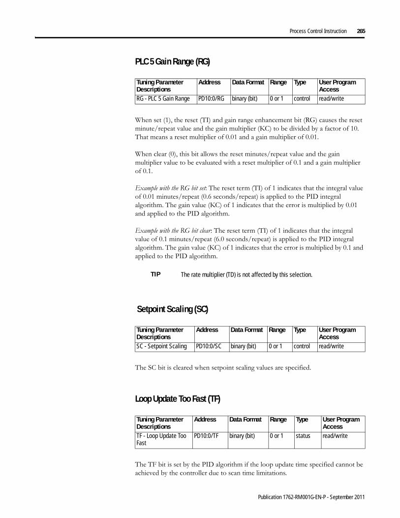
Process Control Instruction 265
PLC 5 Gain Range (RG)
When set (1), the reset (TI) and gain range enhancement bit (RG) causes the reset minute/repeat value and the gain multiplier (KC) to be divided by a factor of 10. That means a reset multiplier of 0.01 and a gain multiplier of 0.01.
When clear (0), this bit allows the reset minutes/repeat value and the gain multiplier value to be evaluated with a reset multiplier of 0.1 and a gain multiplier of 0.1.
Example with the RG bit set: The reset term (TI) of 1 indicates that the integral value of 0.01 minutes/repeat (0.6 seconds/repeat) is applied to the PID integral algorithm. The gain value (KC) of 1 indicates that the error is multiplied by 0.01 and applied to the PID algorithm.
Example with the RG bit clear: The reset term (TI) of 1 indicates that the integral value of 0.1 minutes/repeat (6.0 seconds/repeat) is applied to the PID integral algorithm. The gain value (KC) of 1 indicates that the error is multiplied by 0.1 and applied to the PID algorithm.
Setpoint Scaling (SC)
The SC bit is cleared when setpoint scaling values are specified.
Loop Update Too Fast (TF)
The TF bit is set by the PID algorithm if the loop update time specified cannot be achieved by the controller due to scan time limitations.
Tuning Parameter Descriptions
Address Data Format Range Type User Program Access
RG - PLC 5 Gain Range PD10:0/RG binary (bit) 0 or 1 control read/write
TIP The rate multiplier (TD) is not affected by this selection.
Tuning Parameter Descriptions
Address Data Format Range Type User Program Access
SC - Setpoint Scaling PD10:0/SC binary (bit) 0 or 1 control read/write
Tuning Parameter Descriptions
Address Data Format Range Type User Program Access
TF - Loop Update Too Fast
PD10:0/TF binary (bit) 0 or 1 status read/write
Publication 1762-RM001G-EN-P - September 2011

266 Process Control Instruction
If this bit is set, correct the problem by updating your PID loop at a slower rate or move the PID instruction to an STI interrupt routine. Reset and rate gains will be in error if the instruction operates with this bit set.
Derivative Action Bit (DA)
When set (1), the derivative (rate) action (DA) bit causes the derivative (rate) calculation to be evaluated on the error instead of the process variable (PV). When clear (0), this bit allows the derivative (rate) calculation to be evaluated where the derivative is performed on the PV.
CV Upper Limit Alarm (UL)
The control variable upper limit alarm bit is set when the calculated CV output exceeds the upper CV limit.
CV Lower Limit Alarm (LL)
The control variable lower limit alarm bit is set (1) when the calculated CV output is less than the lower CV limit.
Tuning Parameter Descriptions
Address Data Format Range Type User Program Access
DA - Derivative Action Bit PD10:0/DA binary (bit) 0 or 1 control read/write
Tuning Parameter Descriptions
Address Data Format Range Type User Program Access
UL - CV Upper Limit Alarm PD10:0/UL binary (bit) 0 or 1 status read/write
Tuning Parameter Descriptions
Address Data Format Range Type User Program Access
LL - CV Lower Limit Alarm PD10:0/LL binary (bit) 0 or 1 status read/write
Publication 1762-RM001G-EN-P - September 2011

Process Control Instruction 267
Setpoint Out Of Range (SP)
This bit is set (1) when the setpoint:
• exceeds the maximum scaled value, or• is less than the minimum scaled value.
PV Out Of Range (PV)
The process variable out of range bit is set (1) when the unscaled process variable
• exceeds 16,383, or • is less than zero.
Done (DN)
The PID done bit is set (1) for one scan when the PID algorithm is computed. It resets (0) whenever the instruction is scanned and the PID algorithm was not computed (applies to timed mode only).
Enable (EN)
The PID enabled bit is set (1) whenever the PID instruction is enabled. It follows the rung state.
Tuning Parameter Descriptions
Address Data Format Range Type User Program Access
SP - Setpoint Out of Range PD10:0/SP binary (bit) 0 or 1 status read/write
Tuning Parameter Descriptions
Address Data Format Range Type User Program Access
PV - PV Out of Range PD10:0/PV binary (bit) 0 or 1 status read/write
Tuning Parameter Descriptions
Address Data Format Range Type User Program Access
DN - Done PD10:0/DN binary (bit) 0 or 1 status read only
Tuning Parameter Descriptions
Address Data Format Range Type User Program Access
EN - Enable PD10:0/EN binary (bit) 0 or 1 status read only
Publication 1762-RM001G-EN-P - September 2011

268 Process Control Instruction
Integral Sum (IS)
This is the result of the integration .
Altered Derivative Term (AD)
This long word is used internally to track the change in the process variable within the loop update time.
Runtime Errors Error code 0036 appears in the status file when a PID instruction runtime error occurs. Code 0036 covers the following PID error conditions, each of which has been assigned a unique single byte code value that appears in the MSB of the second word of the control block. The error code is also displayed on the PID Setup Screen in RSLogix 500.
Tuning Parameter Descriptions
Address Data Format Range Type User Program Access
IS - Integral Sum PD10:0.IS long word (32-bit INT)
-2,147,483,648 to 2,147,483,647
status read/write
Tuning Parameter Descriptions
Address Data Format Range Type User Program Access
AD - Altered Derivative Term
PD10:0.AD long word (32-bit INT)
-2,147,483,648 to 2,147,483,647
status read only
KcTI------- E td( )∫
Error Code Description of Error Condition or Conditions Corrective Action11H 1. Loop update time Dt > 1024 Change loop update time 0 < Dt < 1024
2. Loop update time Dt = 0
12H Proportional gain Kc < 0 Change proportional gain Kc to 0 < Kc
13H Integral gain (reset) Ti < 0 Change integral gain (reset) Ti to 0 < Ti
14H Derivative gain (rate) Td < 0 Change derivative gain (rate) Td to 0 < Td
15H Feed Forward Bias (FF) is out-of-range. Change FF so it is within the range -16383 to +16383.
23H Scaled setpoint min MinS > Scaled setpoint max MaxS
Change scaled setpoint min MinS to-32768 < MinS < MaxS < +32767
Publication 1762-RM001G-EN-P - September 2011

Process Control Instruction 269
Analog I/O Scaling To configure an analog input for use in a PID instruction, the analog data must be scaled to match the PID instruction parameters. In the MicroLogix 1200 and 1500, the process variable (PV) in the PID instruction is designed to work with a data range of 0 to 16,383. The 1769 Compact I/O analog modules (1769-IF4 and 1769-OF2) are capable of on-board scaling. Scaling data is required to match the range of the analog input to the input range of the PID instruction. The ability to perform scaling in the I/O modules reduces the amount of programming required in the system and makes PID setup much easier.
The example shows a 1769-IF4 module. The IF4 has 4 inputs, which are individually configurable. In this example, analog input 0 is configured for 0 to 10V and is scaled in engineering units. Word 0 is not being used in a PID instruction. Input 1 (word 1) is configured for 4 to 20 mA operation with scaling configured for a PID instruction. This configures the analog data for the PID instruction.
31H If you are using setpoint scaling and MinS > setpoint SP > MaxS, or
If you are not using setpoint scaling and 0 > setpoint SP > 16383,
then during the initial execution of the PID loop, this error occurs and bit 11 of word 0 of the control block is set. However, during subsequent execution of the PID loop if an invalid loop setpoint is entered, the PID loop continues to execute using the old setpoint, and bit 11 of word 0 of the control block is set.
If you are using setpoint scaling, then change the setpoint SP to MinS < SP < MaxS, or
If you are not using setpoint scaling, then change the setpoint SP to 0 < SP < 16383.
41H Scaling Selected Scaling Deselected Scaling Selected Scaling Deselected1. Deadband < 0, or 1. Deadband < 0, or Change deadband to
0 < deadband < (MaxS - MinS) < 16383
Change deadband to0 < deadband < 163832. Deadband >
(MaxS – MinS)3. Deadband > 16383
51H 1. Output high limit < 0, or
2. Output high limit > 100
Change output high limit to 0 < output high limit < 100
52H 1. Output low limit < 0, or
2. Output low limit > 100
Change output low limit to0 < output low limit < output high limit < 100
53H Output low limit > output high limit Change output low limit to0 < output low limit < output high limit < 100
Error Code Description of Error Condition or Conditions Corrective Action
Field Device Input Signal Analog Register Scaled Data> 20.0 mA 16,384 to 17,406
20.0 mA 16,383
4.0 mA 0
< 4.0 mA -819 to -1
Publication 1762-RM001G-EN-P - September 2011

270 Process Control Instruction
The analog configuration screen is accessed from within RSLogix 500. Simply double click on the I/O configuration item in the “Controller” folder, and then double click on the specific I/O module.
The configuration for the analog output is virtually identical. Simply address the PID control variable (CV) to the analog output address and configure the analog output to “Scaled for PID” behavior.
Application Notes The following paragraphs discuss:
• Input/Output Ranges• Scaling to Engineering Units• Zero-crossing Deadband• Output Alarms• Output Limiting with Anti-reset Windup• The Manual Mode• Feed Forward
Input/Output Ranges
The input module measuring the process variable (PV) must have a full scale binary range of 0 to 16383. If this value is less than 0 (bit 15 set), then a value of
ATTENTION: Do not alter the state of any PID control block value unless you fully understand its function and how it will affect your process. Unexpected operation could result with possible equipment damage and/or personal injury.
Publication 1762-RM001G-EN-P - September 2011

Process Control Instruction 271
zero is used for PV and the “Process var out of range” bit is set (bit 12 of word 0 in the control block). If the process variable is greater than 16383 (bit 14 set), then a value of 16383 is used for PV and the “Process var out of range” bit is set.
The Control Variable, calculated by the PID instruction, has the same range of 0 to 16383. The Control Output (word 16 of the control block) has the range of 0 to 100%. You can set lower and upper limits for the instruction’s calculated output values (where an upper limit of 100% corresponds to a Control Variable limit of 16383).
Scaling to Engineering Units
Scaling lets you enter the setpoint and zero-crossing deadband values in engineering units, and display the process variable and error values in the same engineering units. Remember, the process variable PV must still be within the range 0 to 16383. The PV is displayed in engineering units, however.
Select scaling as follows:
1. Enter the maximum and minimum scaling values MaxS and MinS in the PID control block. The MinS value corresponds to an analog value of zero for the lowest reading of the process variable. MaxS corresponds to an analog value of 16383 for the highest reading. These values reflect the process limits. Setpoint scaling is selected by entering a non-zero value for one or both parameters. If you enter the same value for both parameters, setpoint scaling is disabled.
For example, if measuring a full scale temperature range of -73°C (PV=0) to +1156°C (PV=16383), enter a value of -73 for MinS and 1156 for MaxS. Remember that inputs to the PID instruction must be 0 to 16383. Signal conversions could be as follows:
2. Enter the setpoint (word 2) and deadband (word 9) in the same scaled engineering units. Read the scaled process variable and scaled error in these units as well. The control output percentage (word 16) is displayed as a percentage of the 0 to 16383 CV range. The actual value transferred to the CV output is always between 0 and 16383.
When you select scaling, the instruction scales the setpoint, deadband, process variable, and error. You must consider the effect on all these variables when you change scaling.
Example ValuesProcess limits -73 to +1156°C
Transmitter output (if used) +4 to +20 mA
Output of analog input module 0 to 16383
PID instruction, MinS to MaxS -73 to +1156°C
Publication 1762-RM001G-EN-P - September 2011

272 Process Control Instruction
Zero-Crossing Deadband DB
The adjustable deadband lets you select an error range above and below the setpoint where the output does not change as long as the error remains within this range. This lets you control how closely the process variable matches the setpoint without changing the output.
Zero-crossing is deadband control that lets the instruction use the error for computational purposes as the process variable crosses into the deadband until it crosses the setpoint. Once it crosses the setpoint (error crosses zero and changes sign) and as long as it remains in the deadband, the instruction considers the error value zero for computational purposes.
Select deadband by entering a value in the deadband storage word (word 9) in the control block. The deadband extends above and below the setpoint by the value you enter. A value of zero inhibits this feature. The deadband has the same scaled units as the setpoint if you choose scaling.
Output Alarms
You may set an output alarm on the control variable at a selected value above and/or below a selected output percent. When the instruction detects that the control variable has exceeded either value, it sets an alarm bit (bit LL for lower limit, bit UL for upper limit) in the PID instruction. Alarm bits are reset by the instruction when the control variable comes back inside the limits. The instruction does not prevent the control variable from exceeding the alarm values unless you select output limiting.
Select upper and lower output alarms by entering a value for the upper alarm (CVH) and lower alarm (CVL). Alarm values are specified as a percentage of the output. If you do not want alarms, enter zero and 100% respectively for lower and upper alarm values and ignore the alarm bits.
Output Limiting with Anti-Reset Windup
You may set an output limit (percent of output) on the control variable. When the instruction detects that the control variable has exceeded a limit, it sets an alarm bit (bit LL for lower limit, bit UL for upper limit), and prevents the control variable
Error range
Time
+DB
-DB
SP
Publication 1762-RM001G-EN-P - September 2011

Process Control Instruction 273
from exceeding either limit value. The instruction limits the control variable to 0 and 100% if you choose not to limit.
Select upper and lower output limits by setting the limit enable bit (bit OL), and entering an upper limit (CVH) and lower limit (CVL). Limit values are a percentage (0 to 100%) of the control variable.
The difference between selecting output alarms and output limits is that you must select output limiting to enable limiting. Limit and alarm values are stored in the same words. Entering these values enables the alarms, but not limiting. Entering these values and setting the limit enable bit enables limiting and alarms.
Anti-reset windup is a feature that prevents the integral term from becoming excessive when the control variable reaches a limit. When the sum of the PID and bias terms in the control variable reaches the limit, the instruction stops calculating the integral sum until the control variable comes back in range. The integral sum is contained in element, IS.
The Manual Mode
In the MANUAL mode, the PID algorithm does not compute the value of the control variable. Rather, it uses the value as an input to adjust the integral sum (IS) so that a smooth transfer takes place upon re-entering the AUTO mode.
In the MANUAL mode, the programmer allows you to enter a new CV value from 0 to 100%. This value is converted into a number from 0 to 16383 and written to the Control Variable address. If your ladder program sets the manual output level, design your ladder program to write to the CV address when in the MANUAL mode. Remember that the new CV value is in the range of 0 to 16383, not 0 to 100. Writing to the CV percent (CVP) with your ladder program has no effect in the MANUAL mode.
PID Rung State
If the PID rung is false, the integral sum (IS) is cleared and CV remains in its last state.
Feed Forward or Bias
Applications involving transport lags may require that a bias be added to the CV output in anticipation of a disturbance. This bias can be accomplished using the processor by writing a value to the Feed Forward Bias element (word FF). (See
Publication 1762-RM001G-EN-P - September 2011

274 Process Control Instruction
page 263.) The value you write is added to the output, allowing a feed forward action to take place. You may add a bias by writing a value between -16383 and +16383 to word 6 with your programming terminal or ladder program.
Application Examples PID Tuning
PID tuning requires a knowledge of process control. If you are inexperienced, it will be helpful if you obtain training on the process control theory and methods used by your company.
There are a number of techniques that can be used to tune a PID loop. The following PID tuning method is general and limited in terms of handling load disturbances. When tuning, we recommend that changes be made in the MANUAL mode, followed by a return to AUTO. Output limiting is applied in the MANUAL mode.
Procedure
1. Create your ladder program. Make certain that you have properly scaled your analog input to the range of the process variable PV and that you have properly scaled your control variable CV to your analog output.
2. Connect your process control equipment to your analog modules. Download your program to the processor. Leave the processor in the program mode.
3. Enter the following values: the initial setpoint SP value, a reset Ti of 0, a rate Td of 0, a gain Kc of 1, and a loop update of 5.
Set the PID mode to STI or Timed, per your ladder diagram. If STI is selected, ensure that the loop update time equals the STI time interval.
TIP This method requires that the PID instruction controls a non-critical application in terms of personal safety and equipment damage.
The PID tuning procedure may not work for all cases. It is strongly recommended to use a PID Loop tuner package for the best result (i.e. RSTune, Rockwell Software catalog number 9323-1003D).
ATTENTION: Ensure that all possibilities of machine motion have been considered with respect to personal safety and equipment damage. It is possible that your output CV may swing between 0 and 100% while tuning.
TIP If you want to verify the scaling of your continuous system and/or determine the initial loop update time of your system, go to the procedure on page 276.
Publication 1762-RM001G-EN-P - September 2011

Process Control Instruction 275
Enter the optional settings that apply (output limiting, output alarm, MaxS - MinS scaling, feed forward).
4. Get prepared to chart the CV, PV, analog input, or analog output as it varies with time with respect to the setpoint SP value.
5. Place the PID instruction in the MANUAL mode, then place the processor in the RUN mode.
6. While monitoring the PID display, adjust the process manually by writing to the CO percent value.
7. When you feel that you have the process under control manually, place the PID instruction in the AUTO mode.
8. Adjust the gain while observing the relationship of the output to the setpoint over time.
9. When you notice that the process is oscillating above and below the setpoint in an even manner, record the time of 1 cycle. That is, obtain the natural period of the process.
Natural Period ≅ 4x deadtime
Record the gain value. Return to the MANUAL mode (stop the process if necessary).
10. Set the loop update time (and STI time interval if applicable) to a value of 5 to 10 times faster than the natural period.
For example, if the cycle time is 20 seconds, and you choose to set the loop update time to 10 times faster than the natural rate, set the loop update time to 200, which would result in a 2-second rate.
11. Set the gain Kc value to 1/2 the gain needed to obtain the natural period of the process. For example, if the gain value recorded in step 9 was 80, set the gain to 40.
12. Set the reset term Ti to approximate the natural period. If the natural period is 20 seconds, as in our example, you would set the reset term to 3 (0.3 minutes per repeat approximates 20 seconds).
13. Now set the rate Td equal to a value 1/8 that of the reset term. For our example, the value 4 is used to provide a rate term of 0.04 minutes per repeat.
14. Place the process in the AUTO mode. If you have an ideal process, the PID tuning is complete.
Publication 1762-RM001G-EN-P - September 2011

276 Process Control Instruction
15. To make adjustments from this point, place the PID instruction in the MANUAL mode, enter the adjustment, then place the PID instruction back in the AUTO mode.
This technique of going to MANUAL, then back to AUTO, ensures that most of the “gain error” is removed at the time each adjustment is made. This allows you to see the effects of each adjustment immediately. Toggling the PID rung allows the PID instruction to restart itself, eliminating all of the integral buildup. You may want to toggle the PID rung false while tuning to eliminate the effects of previous tuning adjustments.
Verifying the Scaling of Your Continuous System
To ensure that your process is linear, and that your equipment is properly connected and scaled, do the following:
1. Place the PID instruction in MANUAL and enter the following parameters:
– type: 0 for MinS– type: 100 for MaxS– type: 0 for CO%
2. Enter the REM RUN mode and verify that PV=0.
3. Type: 20 in CO%
4. Record the PV = _______
5. Type: 40 in CO%.
6. Record the PV = _______
7. Type: 60 in CO%.
8. Record the PV = _______
9. Type: 80 in CO%.
10. Record the PV = _______
11. The values you recorded should be offset from CO% by the same amount. This proves the linearity of your process. The following example shows an offset progression of fifteen.– CO 20% = PV 35%– CO 40% = PV 55%– CO 60% = PV 75%
Publication 1762-RM001G-EN-P - September 2011

Process Control Instruction 277
– CO 80% = PV 95%
If the values you recorded are not offset by the same amount:
• Either your scaling is incorrect, or• the process is not linear, or• your equipment is not properly connected and/or configured.
Make the necessary corrections and repeat steps 2-10.
Determining the Initial Loop Update Time
To determine the approximate loop update time that should be used for your process, perform the following:
1. Place the normal application values in MinS and MaxS.
2. Type: 50 in CO%.
3. Type: 60 in CO% and immediately start your stopwatch.
4. Watch the PV. When the PV starts to change, stop your stopwatch. Record this value. It is the deadtime.
5. Multiply the deadtime by 4. This value approximates the natural period. For example, if deadtime = 3 seconds, then 4 x 3 = 12 seconds (≅ natural period)
6. Divide the value obtained in step 5 by 10. Use this value as the loop updated time. For example, if natural period = 12 seconds, then 12/10 = 1.2 seconds.
Therefore, the value 120 would be entered as the loop update time (120 x 10 ms = 1.2 seconds).
7. Enter the following values: the initial setpoint SP value, a reset Ti of 0, a rate Td of 0, a gain Kc of 1, and the loop update time determined in step 17.
Set the PID mode to STI or Timed, per your ladder diagram. If STI is selected, ensure that the loop update time equals the STI time interval.
Enter the optional settings that apply (output limiting, output alarm,MaxS - MinS scaling, feed forward).
8. Return to page 275 and complete the tuning procedure starting with step 4.
Publication 1762-RM001G-EN-P - September 2011

278 Process Control Instruction
Notes:
Publication 1762-RM001G-EN-P - September 2011
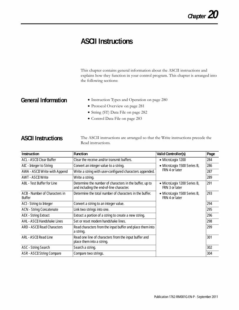
Chapter 20
ASCII Instructions
This chapter contains general information about the ASCII instructions and explains how they function in your control program. This chapter is arranged into the following sections:
General Information • Instruction Types and Operation on page 280• Protocol Overview on page 281• String (ST) Data File on page 282• Control Data File on page 283
ASCII Instructions The ASCII instructions are arranged so that the Write instructions precede the Read instructions.
Instruction Function Valid Controller(s) PageACL - ASCII Clear Buffer Clear the receive and/or transmit buffers. • MicroLogix 1200
• MicroLogix 1500 Series B, FRN 4 or later
284
AIC - Integer to String Convert an integer value to a string. 286
AWA - ASCII Write with Append Write a string with user-configured characters appended. 287
AWT - ASCII Write Write a string. 289
ABL - Test Buffer for Line Determine the number of characters in the buffer, up to and including the end-of-line character.
• MicroLogix 1200 Series B, FRN 3 or later
• MicroLogix 1500 Series B, FRN 4 or later
291
ACB - Number of Characters in Buffer
Determine the total number of characters in the buffer. 293
ACI - String to Integer Convert a string to an integer value. 294
ACN - String Concatenate Link two strings into one. 295
AEX - String Extract Extract a portion of a string to create a new string. 296
AHL - ASCII Handshake Lines Set or reset modem handshake lines. 298
ARD - ASCII Read Characters Read characters from the input buffer and place them into a string.
299
ARL - ASCII Read Line Read one line of characters from the input buffer and place them into a string.
301
ASC - String Search Search a string. 302
ASR - ASCII String Compare Compare two strings. 304
279 Publication 1762-RM001G-EN-P - September 2011

280 ASCII Instructions
Instruction Types and Operation
There are two types of ASCII instructions, ASCII string control and ASCII port control. The string control instruction type is used for manipulating data and executes immediately. The port control instruction type is used for transmitting data and makes use of the ASCII queue. More details are provided below.
ASCII String Control
These instructions are used to manipulate string data. When a string control instruction is encountered in a ladder logic program, it executes immediately. It is never sent to the ASCII queue to wait for execution. The following tables list the ASCII string control instructions used by the MicroLogix 1200 and 1500 controllers:
ASCII Port Control
These instructions use or alter the communication channel for receiving or transmitting data. The following tables list the ASCII port control instructions used by the MicroLogix 1200 and 1500 controllers:
When the ACL (ASCII Clear Buffer) instruction is encountered in a ladder logic program, it executes immediately and causes all instructions to be removed from the ASCII queue, including stopping execution of the ASCII instruction currently executing. The ER (error) bit is set for each instruction that is removed from the ASCII queue.
MicroLogix 1200 Series AAIC (Integer to String)
MicroLogix 1200 Series B, FRN 3 and laterMicroLogix 1500 Series B, FRN 4 and laterACI (String to Integer) AIC (Integer to String)ACN (String Concatenate) ASC (String Search)AEX (String Extract) ASR (ASCII String Compare)
MicroLogix 1200 Series A(1)
(1) For the MicroLogix 1200 Series A, these instructions only transmit data.
ACL (ASCII Clear Buffer)AWA (ASCII Write with Append)AWT (ASCII Write)
MicroLogix 1200 Series B, FRN 3 and laterMicroLogix 1500 Series B, FRN 4 and laterABL (Test Buffer for Line) ARD (ASCII Read Characters)ACB (Number of Characters in Buffer) ARL (ASCII Read Line)ACL (ASCII Clear Buffer) AWA (ASCII Write with Append)AHL (ASCII Handshake Lines) AWT (ASCII Write)
Publication 1762-RM001G-EN-P - September 2011
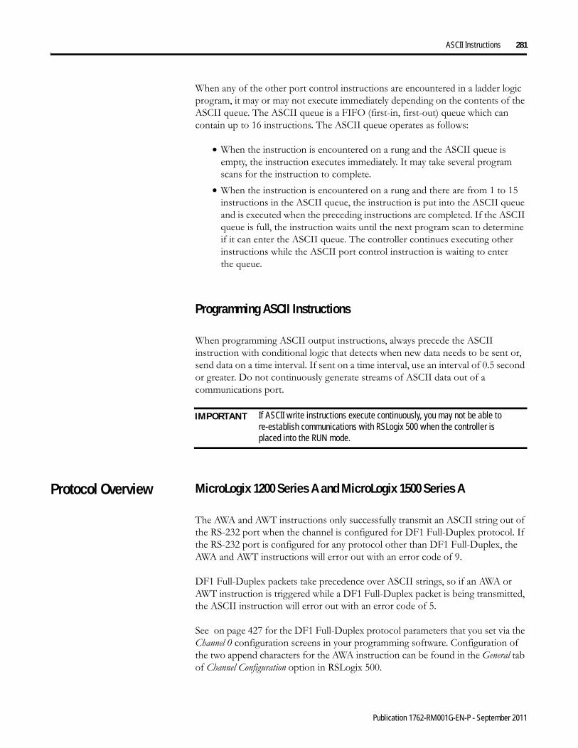
ASCII Instructions 281
When any of the other port control instructions are encountered in a ladder logic program, it may or may not execute immediately depending on the contents of the ASCII queue. The ASCII queue is a FIFO (first-in, first-out) queue which can contain up to 16 instructions. The ASCII queue operates as follows:
• When the instruction is encountered on a rung and the ASCII queue is empty, the instruction executes immediately. It may take several program scans for the instruction to complete.
• When the instruction is encountered on a rung and there are from 1 to 15 instructions in the ASCII queue, the instruction is put into the ASCII queue and is executed when the preceding instructions are completed. If the ASCII queue is full, the instruction waits until the next program scan to determine if it can enter the ASCII queue. The controller continues executing other instructions while the ASCII port control instruction is waiting to enter the queue.
Programming ASCII Instructions
When programming ASCII output instructions, always precede the ASCII instruction with conditional logic that detects when new data needs to be sent or, send data on a time interval. If sent on a time interval, use an interval of 0.5 second or greater. Do not continuously generate streams of ASCII data out of a communications port.
Protocol Overview MicroLogix 1200 Series A and MicroLogix 1500 Series A
The AWA and AWT instructions only successfully transmit an ASCII string out of the RS-232 port when the channel is configured for DF1 Full-Duplex protocol. If the RS-232 port is configured for any protocol other than DF1 Full-Duplex, the AWA and AWT instructions will error out with an error code of 9.
DF1 Full-Duplex packets take precedence over ASCII strings, so if an AWA or AWT instruction is triggered while a DF1 Full-Duplex packet is being transmitted, the ASCII instruction will error out with an error code of 5.
See on page 427 for the DF1 Full-Duplex protocol parameters that you set via the Channel 0 configuration screens in your programming software. Configuration of the two append characters for the AWA instruction can be found in the General tab of Channel Configuration option in RSLogix 500.
IMPORTANT If ASCII write instructions execute continuously, you may not be able to re-establish communications with RSLogix 500 when the controller is placed into the RUN mode.
Publication 1762-RM001G-EN-P - September 2011
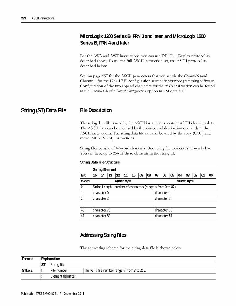
282 ASCII Instructions
MicroLogix 1200 Series B, FRN 3 and later, and MicroLogix 1500 Series B, FRN 4 and later
For the AWA and AWT instructions, you can use DF1 Full-Duplex protocol as described above. To use the full ASCII instruction set, use ASCII protocol as described below.
See on page 457 for the ASCII parameters that you set via the Channel 0 (and Channel 1 for the 1764-LRP) configuration screens in your programming software. Configuration of the two append characters for the AWA instruction can be found in the General tab of Channel Configuration option in RSLogix 500.
String (ST) Data File File Description
The string data file is used by the ASCII instructions to store ASCII character data. The ASCII data can be accessed by the source and destination operands in the ASCII instructions. The string data file can also be used by the copy (COP) and move (MOV, MVM) instructions.
String files consist of 42-word elements. One string file element is shown below. You can have up to 256 of these elements in the string file.
Addressing String Files
The addressing scheme for the string data file is shown below.
String Data File Structure
String ElementBit 15 14 13 12 11 10 09 08 07 06 05 04 03 02 01 00Word upper byte lower byte0 String Length - number of characters (range is from 0 to 82)
1 character 0 character 1
2 character 2 character 3
↓ ↓ ↓40 character 78 character 79
41 character 80 character 81
Format ExplanationST String file
STf:e.s f File number The valid file number range is from 3 to 255.
: Element delimiter
Publication 1762-RM001G-EN-P - September 2011

ASCII Instructions 283
Control Data File File Description
The control data element is used by ASCII instructions to store control information required to operate the instruction. The control data element for ASCII instructions includes status and control bits, an error code byte, and two character words as shown below:
e Element number The valid element number range is from 0 to 255.
Each element is 42 words in length as shown in .
. Subelement delimiter
s Subelement number The valid subelement number range is from 0 to 41.
You can also specify .LEN for word 0 and .DATA[0] through .DATA[40] for words 1 to 41.
The subelement represents a word address.
Examples: ST9:2ST17:1.LENST13:7.DATA[1]
String File 9, Element 2String File 17, Element 1, LEN Variable
String File 13, Element 7, word 2 (characters 2 and 3)
Format Explanation
ASCII Instructions Control Data File Elements
Control ElementWord 15 14 13 12 11 10 09 08 07 06 05 04 03 02 01 000 EN(1)
(1) EN = Enable Bit - indicates that an instruction is enabled due to a false-to-true transition. This bit remains set until the instruction completes execution or generates an error.
EU(2)
(2) EU = Queue Bit - when set, indicates that an ASCII instruction was placed in the ASCII queue. This action is delayed if the queue is already filled.
DN(3)
(3) DN = Asynchronous Done Bit - is set when an instruction successfully completes its operation.
EM(4)
(4) EM = Synchronous Done Bit - not used
ER(5)
(5) ER = Error Bit - when set, indicates that an error occurred while executing the instruction.
UL(6)
(6) UL = Unload Bit - when this bit is set by the user, the instruction does not execute. If the instruction is already executing, operation ceases. If this bit is set while an instruction is executing, any data already processed is sent to the destination and any remaining data is not processed. Setting this bit will not cause instructions to be removed from the ASCII queue. This bit is only examined when the instruction is ready to start executing.
RN(7)
(7) RN = Running Bit - when set, indicates that the queued instruction is executing.
FD(8)
(8) FD = Found Bit - when set, indicates that the instruction has found the end-of-line or termination character in the buffer. (only used by the ABL and ACB instructions)
Error Code Byte
1 Number of characters specified to be sent or received (LEN)
2 Number of characters actually sent or received (POS)
NOTE: The RN bit is not addressable via the Control (R) file.
Publication 1762-RM001G-EN-P - September 2011

284 ASCII Instructions
Addressing Control Files
The addressing scheme for the control data file is shown below.
ACL - ASCII Clear Buffers
Instruction Type: output
Format ExplanationR Control file
R:e.s/b f File number The valid file number range is from 3 to 255.
: Element delimiter
e Element number The valid element number range is from 0 to 255.
Each element is 3 words in length as shown in .
. Subelement delimiter
s Subelement number The valid subelement number range is from 0 to 2. You can also specify .LEN or .POS.
/ Bit delimiter
b Bit number The valid bit number range is from 0 to 15.
The bit number is the bit location within the string file element.
Bit level addressing is not available for words 1 and 2 of the control element.
Examples: R6:2R6:2.0/13R18:1.LENR18:1.POS
Element 2, control file 6Bit 13 in sub-element 0 of element 2, control file 6Specified string length of element 1, control file 18Actual string length of element 1, control file 18
ACLAscii Clear BuffersChannel 0Transmit Buffer YesReceive Buffer No
ACLExecution Time for the ACL Instruction
Controller When Instruction Is:True False
MicroLogix 1200 clear buffers:
both 249.1 μs
receive 28.9 μs
transmit 33.6 μs
0.0 μs
MicroLogix 1500 Series B, FRN 4 or later clear buffers:
both 203.9 μs
receive 24.7 μs
transmit 29.1 μs
0.0 μs
Publication 1762-RM001G-EN-P - September 2011

ASCII Instructions 285
The ACL instruction clears the Receive and/or Transmit buffer(s). This instruction also removes instructions from ASCII queue.
This instruction executes immediately upon the rung transitioning to a true state. Any ASCII transmissions in progress are terminated when the ACL instruction executes.
Entering Parameters
Enter the following parameters when programming this instruction:
• Channel is the number of the RS-232 port, Channel 0. (For the 1764-LRP only, you can select either Channel 0 or Channel 1).
• Receive Buffer clears the Receive buffer when set to “Yes” and removes the Receive ASCII port control instructions (ARL and ARD) from the ASCII queue.
• Transmit Buffer clears the Transmit buffer when set to “Yes” and removes the Transmit ASCII port control instructions (AWA and AWT) from the ASCII queue.
Addressing Modes and File Types can be used as shown below:
TIP For MicroLogix 1200 FRN 7 and MicroLogix 1500 FRN 8 and higher, the ACL instruction can also be used to clear the DF1 communication buffers when the channel is configured for any of the DF1 communication drivers.
Select 0 for the channel number that is configured for DF1 (or 1 for channel 1 on the 1764-LRP only) and Yes for both the Receive and Transmit Buffers. When the ACL instruction is executed, any pending outgoing DF1 replies, any pending incoming DF1 commands and any pending outgoing DF1 commands are flushed. Any MSG instructions in progress on that channel will error out with an error code of 0x0C.
TIP The ASCII queue may contain up to 16 instructions that are waiting to run.
ACL Instruction Valid Addressing Modes and File TypesFor definitions of the terms used in this table see Using the Instruction Descriptions on page 82.
Parameter
Data Files(1) Function Files
CS -
Com
ms
IOS
- I/O
DLS
- D
ata
Log
Address Mode
Address Level
O I S B T, C
, R
N F ST L MG
, PD
PLS
RTC
HSC
PTO
, PW
M
STI
EII
BHI
MM
I
DAT
TPI
Imm
edia
te
Dire
ct
Indi
rect
Bit
Wor
d
Long
Wor
d
Elem
ent
Channel • •
Receive Buffer • •
Transmit Buffer • •
(1) The Control data file is the only valid file type for the Control Element.
Publication 1762-RM001G-EN-P - September 2011

286 ASCII Instructions
Instruction Operation
When Clear Receive Buffer and Clear Transmit Buffer are both set to Yes, all Receive and Transmit instructions (ARL, ARD, AWA, and AWT) are removed from the ASCII queue.
When instructions are removed from the ASCII queue, the following bits are set: ER = 1, RN = 0, EU = 0, and ERR = 0x0E.
AIC - ASCII Integer to String
Instruction Type: output
The AIC instruction converts an integer or long word value (source) to an ASCII string (destination). The source can be a constant or an address. The source data range is from -2,147,483,648 to 2,147,483,647.
Addressing Modes and File Types can be used as shown below:
AICInteger to StringSource N7:0 Dest ST14:1
AICExecution Time for the AIC Instruction
Controller Data Size When Instruction Is:True False
MicroLogix 1200 word 29.3 μs + 5.2 μs/character 0.0 μslong word 82.0 μs 0.0 μs
MicroLogix 1500 Series B, FRN 4 or later word 25 μs + 4.3 μs/character 0.0 μslong word 68.7 μs 0.0 μs
AIC Instruction Valid Addressing Modes and File TypesFor definitions of the terms used in this table see Using the Instruction Descriptions on page 82.
Parameter
Data Files Function Files
CS -
Com
ms
IOS
- I/O
DLS
- Da
ta L
og
Address Mode
Address Level
O I S B T, C
, R
N F ST L MG
, PD
PLS
RTC
HSC
PTO
, PW
M
STI
EII
BHI
MM
I
DAT
TPI
Imm
edia
te
Dire
ct
Indi
rect
Bit
Wor
d
Long
Wor
d
Elem
ent
Source • • • • • • • • • •
Destination • • •
Publication 1762-RM001G-EN-P - September 2011

ASCII Instructions 287
AWA - ASCII Write with Append
Instruction Type: output
Use the AWA instruction to write characters from a source string to an external device. This instruction adds the two appended characters that you configure on the Channel Configuration screen. The default is a carriage return and line feed appended to the end of the string.
Programming AWA Instructions
When programming ASCII output instructions, always precede the ASCII instruction with conditional logic that detects when new data needs to be sent or, send data on a time interval. If sent on a time interval, use an interval of 0.5 second or greater. Do not continuously generate streams of ASCII data out of a communications port.
This instruction will execute on either a false or true rung. However, if you want to repeat this instruction, the rung must go from false-to-true.
When using this instruction you can also perform in-line indirection. See page 305 for more information.
Entering Parameters
Enter the following parameters when programming this instruction:
• Channel is the number of the RS-232 port, Channel 0. (For the 1764-LRP only, you can select either Channel 0 or Channel 1).
EN
DN
ER
AWAASCII Write AppendChannel 0Source ST14:3Control R6:2String Length 12Characters Sent 0 Error 0
AWAExecution Time for the AWA Instruction
Controller When Instruction Is:True False
MicroLogix 1200 268 μs + 12 μs/character 14.1 μsMicroLogix 1500 Series B, FRN 4 or later 236 μs + 10.6 μs/character 12.5 μs
TIP You configure append characters via the Channel Configuration screen. The default append characters are carriage return and line feed.
IMPORTANT If ASCII write instructions execute continuously, you may not be able to re-establish communications with RSLogix 500 when the controller is placed into the RUN mode.
Publication 1762-RM001G-EN-P - September 2011
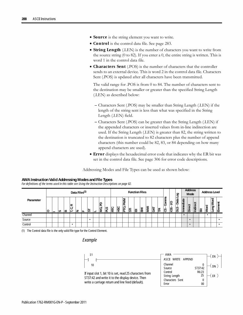
288 ASCII Instructions
• Source is the string element you want to write.• Control is the control data file. See page 283.• String Length (.LEN) is the number of characters you want to write from
the source string (0 to 82). If you enter a 0, the entire string is written. This is word 1 in the control data file.
• Characters Sent (.POS) is the number of characters that the controller sends to an external device. This is word 2 in the control data file. Characters Sent (.POS) is updated after all characters have been transmitted.
The valid range for .POS is from 0 to 84. The number of characters sent to the destination may be smaller or greater than the specified String Length (.LEN) as described below:
– Characters Sent (.POS) may be smaller than String Length (.LEN) if the length of the string sent is less than what was specified in the String Length (.LEN) field.
– Characters Sent (.POS) can be greater than the String Length (.LEN) if the appended characters or inserted values from in-line indirection are used. If the String Length (.LEN) is greater than 82, the string written to the destination is truncated to 82 characters plus the number of append characters (this number could be 82, 83, or 84 depending on how many append characters are used).
• Error displays the hexadecimal error code that indicates why the ER bit was set in the control data file. See page 306 for error code descriptions.
Addressing Modes and File Types can be used as shown below:
Example
AWA Instruction Valid Addressing Modes and File TypesFor definitions of the terms used in this table see Using the Instruction Descriptions on page 82.
Parameter
Data Files(1) Function Files
CS -
Com
ms
IOS
- I/O
DLS
- D
ata
Log
Address Mode
Address Level
O I S B T, C
, R
N F ST L MG
, PD
PLS
RTC
HSC
PTO
, PW
M
STI
EII
BHI
MM
I
DAT
TPI
Imm
edia
te
Dire
ct
Indi
rect
Bit
Wor
d
Long
Wor
d
Elem
ent
Channel • •
Source • • •
Control • • •
(1) The Control data file is the only valid file type for the Control Element.
AWAASCII WRITE APPEND
ChannelSource
I:1
10
[ [
Control
0ST37:42
R6:23String LengthCharacters Sent
250
EN
DN
ER
Error 00
If input slot 1, bit 10 is set, read 25 characters from ST37:42 and write it to the display device. Then write a carriage return and line feed (default).
Publication 1762-RM001G-EN-P - September 2011

ASCII Instructions 289
In this example, when the rung goes from false-to-true, the control element Enable (EN) bit is set. When the instruction is placed in the ASCII queue, the Queue bit (EU) is set. The Running bit (RN) is set when the instruction is executing. The DN bit is set on completion of the instruction.
The controller sends 25 characters from the start of string ST37:42 to the display device and then sends user-configured append characters. The Done bit (DN) is set and a value of 27 is present in .POS word of the ASCII control data file.
When an error is detected, the error code is written to the Error Code Byte and the Error Bit (ER) is set. See ASCII Instruction Error Codes on page 306 for a list of the error codes and recommended action to take.
AWT - ASCII WriteInstruction Type: output
Use the AWT instruction to write characters from a source string to an external device.
Programming AWT Instructions
When programming ASCII output instructions, always precede the ASCII instruction with conditional logic that either detects when new data needs to be sent or, send data on a time interval. If sent on a time interval, use an interval of 0.5 second or greater.
This instruction executes on a true rung. Once started, if the rung goes false, the instruction continues to completion. If you want to repeat this instruction, the rung must transition from false-to-true.
TIP For information on the timing of this instruction, see the timing diagram on page 305.
EN
DN
ER
AWTASCII WriteChannel 0Source ST14:4Control R6:1String Length 40Characters Sent 0 Error 0
AWTExecution Time for the AWT Instruction
Controller When Instruction Is:True False
MicroLogix 1200 268 μs + 12 μs/character 14.1 μsMicroLogix 1500 Series B, FRN 4 or later 237 μs + 10.6 μs/character 12.8 μs
IMPORTANT Do not continuously generate streams of ASCII data out of a communications port. If ASCII write instructions execute continuously, you may not be able to re-establish communications with RSLogix 500 when the controller is placed into the RUN mode.
Publication 1762-RM001G-EN-P - September 2011

290 ASCII Instructions
When using this instruction you can also perform in-line indirection. See page 305 for more information.
Entering Parameters
Enter the following parameters when programming this instruction:
• Channel is the number of the RS-232 port, Channel 0. (For the 1764-LRP only, you can select either Channel 0 or Channel 1).
• Source is the string element you want to write.• Control is the control data file. See page 283.• String Length (.LEN) is the number of characters you want to write from
the source string (0 to 82). If you enter a 0, the entire string is written. This is word 1 in the control data file.
• Characters Sent (.POS) is the number of characters that the controller sends to an external device. This is word 2 in the control data file. Characters Sent (.POS) is updated after all characters have been transmitted.
The valid range for .POS is from 0 to 82. The number of characters sent to the destination may be smaller or greater than the specified String Length (.LEN) as described below:
– Characters Sent (.POS) may be smaller than String Length (.LEN) if the length of the string sent is less than what was specified in the String Length (.LEN) field.
– Characters Sent (.POS) can be greater than the String Length (.LEN) if inserted values from in-line indirection are used. If the String Length (.LEN) is greater than 82, the string written to the destination is truncated to 82 characters.
• Error displays the hexadecimal error code that indicates why the ER bit was set in the control data file. See page 306 for error code descriptions.
Addressing Modes and File Types can be used as shown below:
AWT Instruction Valid Addressing Modes and File TypesFor definitions of the terms used in this table see Using the Instruction Descriptions on page 82.
Parameter
Data Files(1) Function Files
CS -
Com
ms
IOS
- I/O
DLS
- D
ata
Log
Address Mode
Address Level
O I S B T, C
, R
N F ST L MG
, PD
PLS
RTC
HSC
PTO
, PW
M
STI
EII
BHI
MM
I
DAT
TPI
Imm
edia
te
Dire
ct
Indi
rect
Bit
Wor
d
Long
Wor
d
Elem
ent
Channel • •
Source • • •
Control • • •
(1) The Control data file is the only valid file type for the Control Element.
Publication 1762-RM001G-EN-P - September 2011
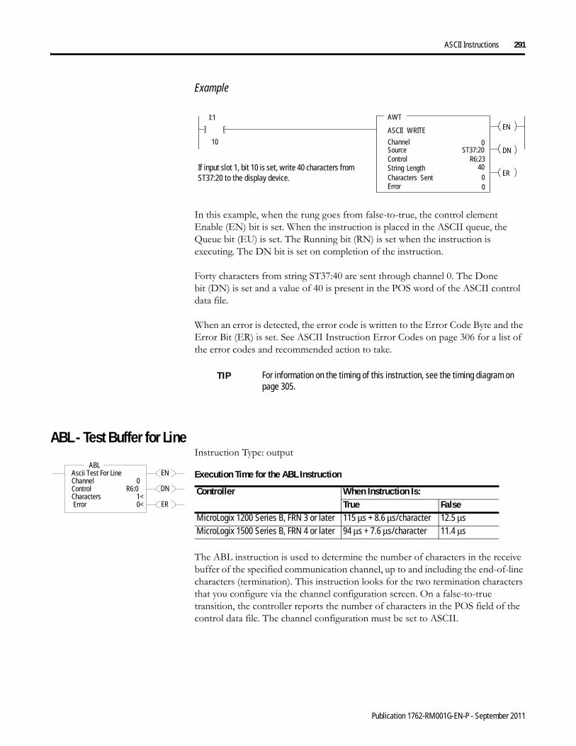
ASCII Instructions 291
Example
In this example, when the rung goes from false-to-true, the control element Enable (EN) bit is set. When the instruction is placed in the ASCII queue, the Queue bit (EU) is set. The Running bit (RN) is set when the instruction is executing. The DN bit is set on completion of the instruction.
Forty characters from string ST37:40 are sent through channel 0. The Done bit (DN) is set and a value of 40 is present in the POS word of the ASCII control data file.
When an error is detected, the error code is written to the Error Code Byte and the Error Bit (ER) is set. See ASCII Instruction Error Codes on page 306 for a list of the error codes and recommended action to take.
ABL - Test Buffer for LineInstruction Type: output
The ABL instruction is used to determine the number of characters in the receive buffer of the specified communication channel, up to and including the end-of-line characters (termination). This instruction looks for the two termination characters that you configure via the channel configuration screen. On a false-to-true transition, the controller reports the number of characters in the POS field of the control data file. The channel configuration must be set to ASCII.
AWT
ASCII WRITE
ChannelSource
I:1
10
[
[
Control
0ST37:20
R6:23String LengthCharacters Sent
4000
EN
DN
ER
Error
If input slot 1, bit 10 is set, write 40 characters from ST37:20 to the display device.
TIP For information on the timing of this instruction, see the timing diagram on page 305.
EN
DN
ER
ABLAscii Test For LineChannel 0Control R6:0Characters 1< Error 0<
ABLExecution Time for the ABL Instruction
Controller When Instruction Is:True False
MicroLogix 1200 Series B, FRN 3 or later 115 μs + 8.6 μs/character 12.5 μsMicroLogix 1500 Series B, FRN 4 or later 94 μs + 7.6 μs/character 11.4 μs
Publication 1762-RM001G-EN-P - September 2011

292 ASCII Instructions
Entering Parameters
Enter the following parameters when programming this instruction:
• Channel is the number of the RS-232 port, Channel 0. (For the 1764-LRP only, you can select either Channel 0 or Channel 1).
• Control is the control data file. See page 283.• Characters are the number of characters in the buffer that the controller
finds (0 to 1024). This parameter is read-only and resides in word 2 of the control data file.
• Error displays the hexadecimal error code that indicates why the ER bit was set in the control data file. See page 306 for error code descriptions.
Addressing Modes and File Types can be used as shown below:
Instruction Operation
When the rung goes from false-to-true, the Enable bit (EN) is set. The instruction is put in the ASCII instruction queue, the Queue bit (EU) is set, and program scan continues. The instruction is then executed outside of the program scan. However, if the queue is empty the instruction executes immediately. Upon execution, the Run bit (RN) is set.
The controller determines the number of characters (up to and including the termination characters) and puts this value in the POS field of the control data file. The Done bit (DN) is then set. If a zero appears in the POS field, no termination characters were found. The Found bit (FD) is set if the POS field is set to a non-zero value.
ABL Instruction Valid Addressing Modes and File TypesFor definitions of the terms used in this table see Using the Instruction Descriptions on page 82.
Parameter
Data Files(1) Function Files
CS -
Com
ms
IOS
- I/O
DLS
- Da
ta L
og
Address Mode
Address Level
O I S B T, C
, R
N F ST L MG
, PD
PLS
RTC
HSC
PTO
, PW
M
STI
EII
BHI
MM
I
DAT
TPI
Imm
edia
te
Dire
ct
Indi
rect
Bit
Wor
d
Long
Wor
d
Elem
ent
Channel • •
Control • • •
(1) The Control data file is the only valid file type for the Control Element.
Publication 1762-RM001G-EN-P - September 2011

ASCII Instructions 293
ACB - Number of Characters in Buffer
Instruction Type: output
Use the ACB instruction to determine the number of characters in the buffer. On a false-to-true transition, the controller determines the total number of characters and records it in the POS field of the control data file. The channel configuration must be set to ASCII.
Entering Parameters
Enter the following parameters when programming this instruction:
• Channel is the number of the RS-232 port, Channel 0. (For the 1764-LRP only, you can select either Channel 0 or Channel 1).
• Control is the control data file. See page 283.• Characters are the number of characters in the buffer that the controller
finds (0 to 1024). This parameter is read-only.• Error displays the hexadecimal error code that indicates why the ER bit
was set in the control data file. See page 306 for error descriptions.
Addressing Modes and File Types can be used as shown below:
EN
DN
ER
ACBAscii Chars In BufferChannel 0Control R6:1Characters 2<
Error 0<
ACBExecution Time for the ACB Instruction
Controller When Instruction Is:True False
MicroLogix 1200 Series B, FRN 3 or later 103.1 12.1MicroLogix 1500 Series B, FRN 4 or later 84.2 μs 11.0 μs
ACB Instruction Valid Addressing Modes and File TypesFor definitions of the terms used in this table see Using the Instruction Descriptions on page 82.
Parameter
Data Files(1) Function Files
CS -
Com
ms
IOS
- I/O
DLS
- D
ata
Log
Address Mode
Address Level
O I S B T, C
, R
N F ST L MG
, PD
PLS
RTC
HSC
PTO
, PW
M
STI
EII
BHI
MM
I
DAT
TPI
Imm
edia
te
Dir
ect
Indi
rect
Bit
Wor
d
Long
Wor
d
Elem
ent
Channel • •
Control • • •
(1) The Control data file is the only valid file type for the Control Element.
Publication 1762-RM001G-EN-P - September 2011

294 ASCII Instructions
Instruction Operation
When the rung goes from false-to-true, the Enable bit (EN) is set. When the instruction is placed in the ASCII queue, the Queue bit (EU) is set. The Running bit (RN) is set when the instruction is executing. The Done bit (DN) is set on completion of the instruction.
The controller determines the number of characters in the buffer and puts this value in the POS field of the control data file. The Done bit (DN) is then set. If a zero appears in the POS field, no characters were found. The Found bit (FD) is set when the POS filed is set to a non-zero value
ACI - String to IntegerInstruction Type: output
Use the ACI instruction to convert a numeric ASCII string to an integer (word or long word) value.
Entering Parameters
Enter the following parameters when programming this instruction:
• Source - The contents of this location are converted to an integer value.• Destination - This is the location which receives the result of the
conversion. The data range is from -32,768 to 32,767 if the destination is a word and from -2,147,483,648 to 2,147,483,647 if the destination is a long word.
ACIString to IntegerSource ST10:0Dest N7:0 0<
ACIExecution Time for the ACI Instruction
Controller Data Size When Instruction Is:True False
MicroLogix 1200 Series B, FRN 3 or later
word 17.6 μs + 7.2 μs/character 0.0 μslong word 24.6 μs + 11.6 μs/character 0.0 μs
MicroLogix 1500 Series B, FRN 4 or later
14.2 μs + 6.3 μs/character 0.0 μs
Publication 1762-RM001G-EN-P - September 2011

ASCII Instructions 295
Addressing Modes and File Types can be used as shown below:
Instruction Operation
The controller searches the source (file type ST) for the first character between 0 and 9. All numeric characters are extracted until a non-numeric character or the end of the string is reached. Action is taken only if numeric characters are found. The string length is limited to 82 characters. Commas and signs (+, -) are allowed in the string. However, only the minus sign is displayed in the data table.
This instruction sets the following math flags in the controller status file:
ACN - String Concatenate Instruction Type: output
The ACN instruction combines two ASCII strings. The second string is appended to the first and the result stored in the destination.
ACI Instruction Valid Addressing Modes and File TypesFor definitions of the terms used in this table see Using the Instruction Descriptions on page 82.
Parameter
Data Files(1) Function Files
CS -
Com
ms
IOS
- I/O
DLS
- Da
ta L
og
Address Mode
Address Level
O I S B T, C
, R
N F ST L MG
, PD
PLS
RTC
HSC
PTO
, PW
M
STI
EII
BHI
MM
I
DAT
TPI
Imm
edia
te
Dir
ect
Indi
rect
Bit
Wor
d
Long
Wor
d
Elem
ent
Source • • •
Destination • • • • • • • •
(1) The Control data file is the only valid file type for the Control Element.
Math Flag DescriptionS:0/1 Overflow (V) Flag is set if the result is outside of the valid range.
S:0/2 Zero (Z) Flag is set if the result is zero.
S:0/3 Sign (S) Flag is set if the result is negative.
S:5/0 Overflow Trap Flag is set when the Overflow flag (S:0/1) is set.
S:5/15 ASCII String Manipulation Error
Flag is set if the Source string exceeds 82 characters.
When S:5/15 is set, the Invalid String Length Error (1F39H) is written to the Major Error Fault Code (S:6).
ACNString ConcatenateSource A ST10:11Source B ST10:12Dest ST10:10
ACN Execution Time for the ACN Instruction
Controller When Instruction Is:True False
MicroLogix 1200 Series B, FRN 3 or later 22.6 μs + 11.5 μs/character 0.0 μsMicroLogix 1500 Series B, FRN 4 or later 17.9 μs + 10.2 μs/character 0.0 μs
Publication 1762-RM001G-EN-P - September 2011
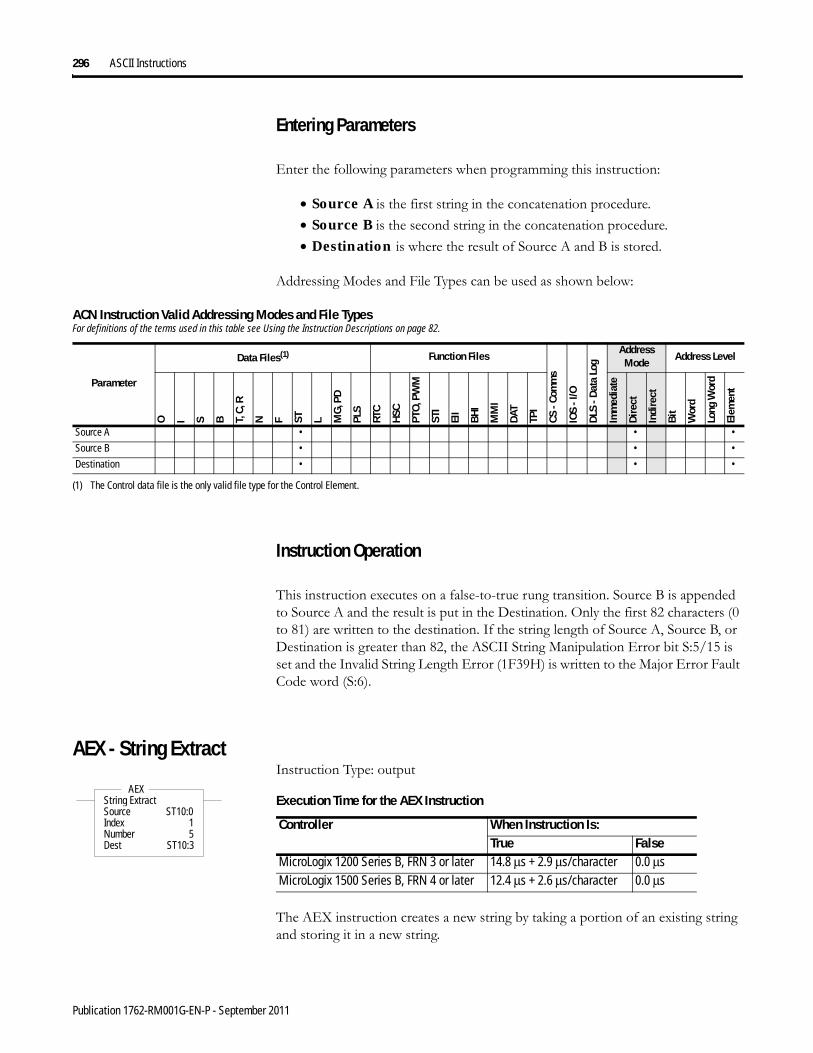
296 ASCII Instructions
Entering Parameters
Enter the following parameters when programming this instruction:
• Source A is the first string in the concatenation procedure.• Source B is the second string in the concatenation procedure.• Destination is where the result of Source A and B is stored.
Addressing Modes and File Types can be used as shown below:
Instruction Operation
This instruction executes on a false-to-true rung transition. Source B is appended to Source A and the result is put in the Destination. Only the first 82 characters (0 to 81) are written to the destination. If the string length of Source A, Source B, or Destination is greater than 82, the ASCII String Manipulation Error bit S:5/15 is set and the Invalid String Length Error (1F39H) is written to the Major Error Fault Code word (S:6).
AEX - String ExtractInstruction Type: output
The AEX instruction creates a new string by taking a portion of an existing string and storing it in a new string.
ACN Instruction Valid Addressing Modes and File TypesFor definitions of the terms used in this table see Using the Instruction Descriptions on page 82.
Parameter
Data Files(1) Function Files
CS -
Com
ms
IOS
- I/O
DLS
- D
ata
Log
Address Mode
Address Level
O I S B T, C
, R
N F ST L MG
, PD
PLS
RTC
HSC
PTO
, PW
M
STI
EII
BHI
MM
I
DAT
TPI
Imm
edia
te
Dir
ect
Indi
rect
Bit
Wor
d
Long
Wor
d
Elem
ent
Source A • • •
Source B • • •
Destination • • •
(1) The Control data file is the only valid file type for the Control Element.
AEXString ExtractSource ST10:0Index 1Number 5Dest ST10:3
AEXExecution Time for the AEX Instruction
Controller When Instruction Is:True False
MicroLogix 1200 Series B, FRN 3 or later 14.8 μs + 2.9 μs/character 0.0 μsMicroLogix 1500 Series B, FRN 4 or later 12.4 μs + 2.6 μs/character 0.0 μs
Publication 1762-RM001G-EN-P - September 2011

ASCII Instructions 297
Entering Parameters
Enter the following parameters when programming this instruction:
• Source is the existing string. The Source value is not affected by this instruction.
• Index is the starting position (from 1 to 82) of the string you want to extract. (An index of 1 indicates the left-most character of the string.)
• Number is the number of characters (from 1 to 82) you want to extract, starting at the indexed position. If the Index plus the Number is greater than the total characters in the source string, the Destination string will be the characters from the Index to the end of the Source string.
• Destination is the string element (ST) where you want the extracted string stored.
Addressing Modes and File Types can be used as shown below:
Instruction Operation
This instruction executes on a true rung.
The following conditions cause the controller to set the ASCII String Manipulation Error bit (S:5/15):
• Source string length is less than 1 or greater than 82• Index value is less than 1 or greater than 82• Number value is less than 1 or greater than 82• Index value greater than the length of the Source string
The Destination string is not changed in any of the above error conditions. When the ASCII String Manipulation Error bit (S:5/15) is set, the Invalid String Length Error (1F39H) is written to the Major Error Fault Code word (S:6).
AEX Instruction Valid Addressing Modes and File TypesFor definitions of the terms used in this table see Using the Instruction Descriptions on page 82.
Parameter
Data Files(1) Function Files
CS -
Com
ms
IOS
- I/O
DLS
- D
ata
Log
Address Mode
Address Level
O I S B T, C
, R
N F ST L MG
, PD
PLS
RTC
HSC
PTO
, PW
M
STI
EII
BHI
MM
I
DAT
TPI
Imm
edia
te
Dir
ect
Indi
rect
Bit
Wor
d
Long
Wor
d
Elem
ent
Source • • •
Index • • • • • • •
Number • • • • • • •
Destination • • •
(1) The Control data file is the only valid file type for the Control Element.
Publication 1762-RM001G-EN-P - September 2011

298 ASCII Instructions
AHL - ASCII Handshake Lines
Instruction Type: output
The AHL instruction is used to set or reset the RS-232 Request to Send (RTS) handshake control line for a modem. The controller uses the two masks to determine whether to set or reset the RTS control line, or leave it unchanged. The channel configuration must be set to ASCII.
Entering Parameters
Enter the following parameters when programming this instruction:
• Channel is the number of the RS-232 port, Channel 0. (For the 1764-LRP only, you can select either Channel 0 or Channel 1.)
• AND Mask is the mask used to reset the RTS control line. Bit 1 corresponds to the RTS control line. A value of “2” in the AND mask resets the RTS control line; a value of “0” leaves the line unchanged.
• OR Mask is the mask used to set the RTS control line. Bit 1 corresponds to the RTS control line. A value of “2” in the OR mask sets the RTS control line; a value of “0” leaves the line unchanged.
• Control is the control data file. See page 283.• Channel Status displays the current status (0000 to 001F) of the
handshake lines for the specified channel. This status is read-only and resides in the .POS field in the control data file. The following shows how to determine the channel status value. In this example, the value is 001F.
EN
DN
ER
AHLAscii Handshake LinesChannel 0AND Mask 0002hOR Mask 0000hControl R6:2Channel Status 0000h<
Error 0<
AHLExecution Time for the AHL Instruction
Controller When Instruction Is:True False
MicroLogix 1200 Series B, FRN 3 or later 109.4 μs 11.9 μsMicroLogix 1500 Series B, FRN 4 or later 89.3 μs 10.8 μs
TIP Make sure the automatic modem control used by the port does not conflict with this instruction.
Channel Status Bit
15 14 13 12 11 10 9 8 7 6 5 4 3 2 1 0
Handshake Control Line Setting
reserved -- DCD(1)
(1) The DCD handshake line is only supported on Channel 1.
-- RTS CTS
0 0 0 0 0 0 0 0 0 0 0 1 1 1 1 1
Channel Status
0 0 1 F
Word 2 of the Control Element = 001F
Publication 1762-RM001G-EN-P - September 2011

ASCII Instructions 299
• Error displays the hexadecimal error code that indicates why the ER bit was set in the control data file. See page 306 for error code descriptions.
Addressing Modes and File Types can be used as shown below:
Instruction Operation
This instruction executes on either a false or true rung. However a false-to-true rung transition is required to set the EN bit to repeat the instruction.
ARD - ASCII Read Characters
Instruction Type: output
Use the ARD instruction to read characters from the buffer and store them in a string. To repeat the operation, the rung must go from false-to-true.
Entering Parameters
Enter the following parameters when programming this instruction:
• Channel is the number of the RS-232 port, Channel 0. (For the 1764-LRP only, you can select either Channel 0 or Channel 1).
AHL Instruction Valid Addressing Modes and File TypesFor definitions of the terms used in this table see Using the Instruction Descriptions on page 82.
Parameter
Data Files(1) Function Files
CS -
Com
ms
IOS
- I/O
DLS
- Da
ta L
og
Address Mode
Address Level
O I S B T, C
, R
N F ST L MG
, PD
PLS
RTC
HSC
PTO
, PW
M
STI
EII
BHI
MM
I
DAT
TPI
Imm
edia
te
Dir
ect
Indi
rect
Bit
Wor
d
Long
Wor
d
Elem
ent
Channel • •
AND Mask • • • • • • • •
OR Mask • • • • • • • •
Control • • •
(1) The Control data file is the only valid file type for the Control Element.
EN
DN
ER
ARDASCII ReadChannel 0Dest ST10:4Control R6:3String Length 10<Characters Read 0< Error 0<
ARDExecution Time for the ARD Instruction
Controller When Instruction Is:True False
MicroLogix 1200 Series B, FRN 3 or later 132.3 μs + 49.7 μs/character 11.8 μsMicroLogix 1500 Series B, FRN 4 or later 108 μs + 44 μs/character 10.7 μs
Publication 1762-RM001G-EN-P - September 2011

300 ASCII Instructions
• Destination is the string element where you want the characters stored.• Control is the control data file. See page 283.• String Length (LEN) is the number of characters you want to read from
the buffer. The maximum is 82 characters. If you specify a length larger than 82, only the first 82 characters will be read. If you specify 0 characters, LEN defaults to 82. This is word 1 in the control data file.
• Characters Read (POS) is the number of characters that the controller moved from the buffer to the string (0 to 82). This field is updated during the execution of the instruction and is read-only. This is word 2 in the control data file.
• Error displays the hexadecimal error code that indicates why the ER bit was set in the control data file. See page 306 for error code descriptions.
Addressing Modes and File Types can be used as shown below:
Instruction Operation
When the rung goes from false-to-true, the Enable bit (EN) is set. When the instruction is placed in the ASCII queue, the Queue bit (EU) is set. The Running bit (RN) is set when the instruction is executing. The DN bit is set on completion of the instruction.
Once the requested number of characters are in the buffer, the characters are moved to the destination string. The number of characters moved is put in the POS field of the control data file. The number in the POS field is continuously updated and the Done bit (DN) is not set until all of the characters are read.
ARD Instruction Valid Addressing Modes and File TypesFor definitions of the terms used in this table see Using the Instruction Descriptions on page 82.
Parameter
Data Files(1) Function Files
CS -
Com
ms
IOS
- I/O
DLS
- D
ata
Log
Address Mode
Address Level
O I S B T, C
, R
N F ST L MG
, PD
PLS
RTC
HSC
PTO
, PW
M
STI
EII
BHI
MM
I
DAT
TPI
Imm
edia
te
Dir
ect
Indi
rect
Bit
Wor
d
Long
Wor
d
Elem
ent
Channel • •
Destination • • •
Control • • •
(1) The Control data file is the only valid file type for the Control Element.
TIP For information on the timing of this instruction, see the timing diagram on page 305.
Publication 1762-RM001G-EN-P - September 2011

ASCII Instructions 301
ARL - ASCII Read LineInstruction Type: output
Use the ARL instruction to read characters from the buffer, up to and including the Termination characters, and store them in a string. The Termination characters are specified via the Channel Configuration screen.
Entering Parameters
Enter the following parameters when programming this instruction:
• Channel is the number of the RS-232 port, Channel 0. (For the 1764-LRP only, you can select either Channel 0 or Channel 1).
• Destination is the string element where you want the string stored.• Control is the control data file. See page 283.• String Length (LEN) is the number of characters you want to read from
the buffer. The maximum is 82 characters. If you specify a length larger than 82, only the first 82 characters are read and moved to the destination. (A length of “0” defaults to 82.) This is word 1 in the control data file.
• Characters Read (POS) is the number of characters that the controller moved from the buffer to the string (0 to 82). This field is read-only and resides in word 2 of the control data file.
• Error displays the hexadecimal error code that indicates why the ER bit was set in the control data file. See page 306 for error code descriptions.
Addressing Modes and File Types can be used as shown below:
EN
DN
ER
ARLASCII Read LineChannel 0Dest ST10:5Control R6:4String Length 15<Characters Read 0<
Error 0<
ARLExecution Time for the ARL Instruction
Controller When Instruction Is:True False
MicroLogix 1200 Series B, FRN 3 or later 139.7 μs + 50.1 μs/character 11.7 μsMicroLogix 1500 Series B, FRN 4 or later 114 μs + 44.3 μs/character 10.6 μs
ARL Instruction Valid Addressing Modes and File TypesFor definitions of the terms used in this table see Using the Instruction Descriptions on page 82.
Parameter
Data Files(1) Function Files
CS -
Com
ms
IOS
- I/O
DLS
- Da
ta L
og
Address Mode
Address Level
O I S B T, C
, R
N F ST L MG
, PD
PLS
RTC
HSC
PTO
, PW
M
STI
EII
BHI
MM
I
DAT
TPI
Imm
edia
te
Dire
ct
Indi
rect
Bit
Wor
d
Long
Wor
d
Elem
ent
Channel • •
Destination • • •
Control • • •
(1) The Control data file is the only valid file type for the Control Element.
Publication 1762-RM001G-EN-P - September 2011

302 ASCII Instructions
Instruction Operation
When the rung goes from false-to-true, the control element Enable (EN) bit is set. When the instruction is placed in the ASCII queue, the Queue bit (EU) is set. The Running bit (RN) is set when the instruction is executing. The DN bit is set on completion of the instruction.
Once the requested number of characters are in the buffer, all characters (including the Termination characters) are moved to the destination string. The number of characters moved is stored in the POS word of the control data file. The number in the Characters Read field is continuously updated and the Done bit (DN) is not set until all of the characters have been read. Exception: If the controller finds termination characters before done reading, the Done bit (DN) is set and the number of characters found is stored in the POS word of the control data file.
ASC - String SearchInstruction Type: output
Use the ASC instruction to search an existing string for an occurrence of the source string. This instruction executes on a true rung.
Entering Parameters
Enter the following parameters when programming this instruction:
• Source is the address of the string you want to find.• Index is the starting position (from 1 to 82) within the search string. (An
index of 1 indicates the left-most character of the string.)• Search is the address of the string you want to examine.• Result is the location (from 1 to 82) that the controller uses to store the
position in the Search string where the Source string begins. If no match is found, result is set equal to zero.
TIP For information on the timing of this instruction, see the timing diagram on page 305.
ASCString SearchSource ST10:6Index 5String Search ST10:7Result N7:1 0<
ASCExecution Time for the ASC Instruction
Controller When Instruction Is:True False
MicroLogix 1200 Series B, FRN 3 or later 16.2 μs + 4.0 μs/matching character 0.0 μsMicroLogix 1500 Series B, FRN 4 or later 13.4 μs + 3.5 μs/matching character 0.0 μs
Publication 1762-RM001G-EN-P - September 2011
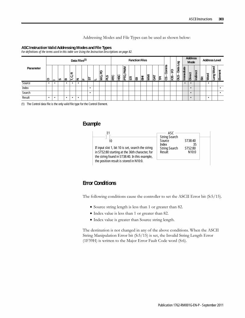
ASCII Instructions 303
Addressing Modes and File Types can be used as shown below:
Example
Error Conditions
The following conditions cause the controller to set the ASCII Error bit (S:5/15).
• Source string length is less than 1 or greater than 82.• Index value is less than 1 or greater than 82.• Index value is greater than Source string length.
The destination is not changed in any of the above conditions. When the ASCII String Manipulation Error bit (S:5/15) is set, the Invalid String Length Error (1F39H) is written to the Major Error Fault Code word (S:6).
ASC Instruction Valid Addressing Modes and File TypesFor definitions of the terms used in this table see Using the Instruction Descriptions on page 82.
Parameter
Data Files(1) Function Files
CS -
Com
ms
IOS
- I/O
DLS
- Da
ta L
og
Address Mode
Address Level
O I S B T, C
, R
N F ST L MG
, PD
PLS
RTC
HSC
PTO
, PW
M
STI
EII
BHI
MM
I
DAT
TPI
Imm
edia
te
Dir
ect
Indi
rect
Bit
Wor
d
Long
Wor
d
Elem
ent
Source • • • • • • • •
Index • • •
Search • • •
Result • • • • • • •
(1) The Control data file is the only valid file type for the Control Element.
I:1
10
ASCString SearchSource ST38:40Index 35String Search ST52:80Result N10:0
ASC
If input slot 1, bit 10 is set, search the string in ST52:80 starting at the 36th character, for the string found in ST38:40. In this example, the position result is stored in N10:0.
Publication 1762-RM001G-EN-P - September 2011
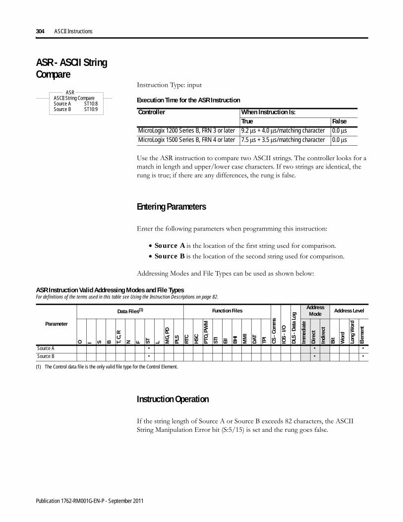
304 ASCII Instructions
ASR - ASCII String Compare
Instruction Type: input
Use the ASR instruction to compare two ASCII strings. The controller looks for a match in length and upper/lower case characters. If two strings are identical, the rung is true; if there are any differences, the rung is false.
Entering Parameters
Enter the following parameters when programming this instruction:
• Source A is the location of the first string used for comparison.• Source B is the location of the second string used for comparison.
Addressing Modes and File Types can be used as shown below:
Instruction Operation
If the string length of Source A or Source B exceeds 82 characters, the ASCII String Manipulation Error bit (S:5/15) is set and the rung goes false.
ASRASCII String CompareSource A ST10:8Source B ST10:9
ASRExecution Time for the ASR Instruction
Controller When Instruction Is:True False
MicroLogix 1200 Series B, FRN 3 or later 9.2 μs + 4.0 μs/matching character 0.0 μsMicroLogix 1500 Series B, FRN 4 or later 7.5 μs + 3.5 μs/matching character 0.0 μs
ASR Instruction Valid Addressing Modes and File TypesFor definitions of the terms used in this table see Using the Instruction Descriptions on page 82.
Parameter
Data Files(1) Function Files
CS -
Com
ms
IOS
- I/O
DLS
- D
ata
Log
Address Mode
Address Level
O I S B T, C
, R
N F ST L MG
, PD
PLS
RTC
HSC
PTO
, PW
M
STI
EII
BHI
MM
I
DAT
TPI
Imm
edia
te
Dir
ect
Indi
rect
Bit
Wor
d
Long
Wor
d
Elem
ent
Source A • • •
Source B • • •
(1) The Control data file is the only valid file type for the Control Element.
Publication 1762-RM001G-EN-P - September 2011

ASCII Instructions 305
Timing Diagram for ARD, ARL, AWA, and AWT Instructions
Using In-line Indirection This allows you to insert integer and long word values into ASCII strings. The Running bit (RN) must be set before the string value can be used.
The following conditions apply to performing in-line indirection:
• All valid integer (N) and long word (L) files can be used. Valid range is from 3 to 255.
• File types are not case sensitive and can include either a colon (:) or semicolon (;)
• Positive value symbol (+) and leading zeros are not printed. Negative values (-) are printed with a leading minus sign. Commas are not inserted where they would normally appear in numbers greater than one thousand.
1 2 6 3 4 5 1 5 2 6 3 4
Rung Condition
Enable Bit (EN)
Queue Bit (EU)
Running Bit (RN)
Done BitError Bit(DN or ER)
ONOFF
ONOFF
ONOFF
ONOFF
ONOFF
1 - rung goes true2 - instruction successfully queued3 - instruction execution complete4 - instruction scanned for the first time after execution is complete5 - rung goes false6 - instruction execution starts
NOTE: The RN bit is not addressable via the Control (R) file.
Publication 1762-RM001G-EN-P - September 2011

306 ASCII Instructions
Examples
For the following examples:N7:0 = 25N7:1 = -37L8:0 = 508000L8:1 = 5
ASCII Instruction Error Codes
The following error codes indicate why the Error bit (ER) is set in the control data file.
Valid in-line direction:Input: Flow rate is currently [N7:0] liters per minute and contains [L8:0] particles per liter
contaminants.
Output: Flow rate is currently 25 liters per minute and contains 508000 particles per liter contaminants.
Input: Current position is [N7:1] at a speed of [L8:1] RPM.
Output: Current position is -37 at a speed of 5 RPM.
Invalid in-line indirection:Input: Current position is [N5:1] at a speed of [L8:1] RPM.
Output: Current position is [N5:1] at a speed of 5 RPM.
TIP Truncation occurs in the output string if the indirection causes the output to exceed 82 characters. The appended characters are always applied to the output.
Error Code Description Recommended Actiondecimal hexadecimal0 0x00 No error. The instruction completed successfully. None Required.
3 0x03 The transmission cannot be completed because the CTS signal was lost.
Check the modem and modem connections.
5 0x05 While attempting to perform an ASCII transmission, a conflict with the configured communications protocol was detected.
Reconfigure the channel and retry operation.
7 0x07 The instruction cannot be executed because the communications channel has been shut down via the channel configuration menu.
Reconfigure the channel and retry operation.
8 0x08 The instruction cannot be executed because another ASCII transmission is already in progress.
Resend the transmission.
9 0x09 Type of ASCII communications operation requested is not supported by the current channel configuration.
Reconfigure the channel and retry operation.
10 0x0A The unload bit (UL) is set, stopping instruction execution. None required.
11 0x0B The requested number of characters for the ASCII read was too large or negative.
Enter a valid string length and retry operation.
12 0x0C The length of the Source string is invalid (either a negative number or a number greater than 82).
Enter a valid string length and retry operation.
Publication 1762-RM001G-EN-P - September 2011

ASCII Instructions 307
ASCII Character Set The table below lists the decimal, hexadecimal, octal, and ASCII conversions.
The standard ASCII character set includes values up to 127 decimal (7F hex). The MicroLogix 1200 and 1500 Controllers also support an extended character set (decimal 128 to 255). However, the extended character set may display different characters depending on the platform you are using.
Decimal values 0 through 31 are also assigned Ctrl- codes.
13 0x0D The requested length in the Control field is invalid (either a negative number or a number greater than 82).
Enter a valid length and retry operation.
14 0x0E Execution of an ACL instruction caused this instruction to abort. None required.
15 0x0F Communications channel configuration was changed while instruction was in progress.
None required.
Error Code Description Recommended Actiondecimal hexadecimal
Standard ASCII Character Set
Column 1 Column 2 Column 3 Column 4Ctrl- DEC HEX OCT ASC DEC HEX OCT ASC DEC HEX OCT ASC DEC HEX OCT ASC
^@^A^B^C^D^E^F^G^H^I^J^K^L^M^N^O^P^Q^R^S^T^U^V^W^X^Y^Z^[^\^]^^^_
0001020304050607080910111213141516171819202122232425262728293031
000102030405060708090A0B0C0D0E0F101112131415161718191A1B1C1D1E1F
000001002003004005006007010011012013014015016017020021022023024025026027030031032033034035036037
NULSOHSTXETXEOTENQACKBELBSHTLFVTFFCRSOSIDLEDC1DC2DC3DC4NAKSYNETBCANEMSUBESCFSGSRSUS
3233343536373839404142434445464748495051525354555657585960616263
202122232425262728292A2B2C2D2E2F303132333435363738393A3B3C3D3E3F
040041042043044045046047050051052053054055056057060061062063064065066067070071072073074075076077
SP!“#$%&'()*+,-./0123456789:;<=>?
6465666768697071727374757677787980818283848586878889909192939495
404142434445464748494A4B4C4D4E4F505152535455565758595A5B5C5D5E5F
100101102103104105106107110111112113114115116117120121122123124125126127130131132133134135136137
@ABCDEFGHIJKLMNOPQRSTUVWXYZ[\]^_
96979899100101102103104105106107108109110111112113114115116117118119120121122123124125126127
606162636465666768696A6B6C6D6E6F707172737475767778797A7B7C7D7E7F
140141142143144145146147150151152153154155156157160161162163164165166167170171172173174175176177
\abcdefghijklmnopqrstuvwxyz{|}~DEL
Publication 1762-RM001G-EN-P - September 2011

308 ASCII Instructions
Notes:
Publication 1762-RM001G-EN-P - September 2011

Chapter 21
Communications Instructions
This chapter contains information about the Message (MSG) and Service Communications (SVC), communication instructions. This chapter provides information on:
• Messaging Overview on page 309• SVC - Service Communications on page 310• MSG - Message on page 313• The Message Element on page 314• Timing Diagram for the MSG Instruction on page 320• MSG Instruction Ladder Logic on page 323• Local Messages on page 324• Configuring a Local Message on page 325• Local Messaging Examples on page 333• Remote Messages on page 346• Configuring a Remote Message on page 348• MSG Instruction Error Codes on page 351
The communication instructions read or write data to another station.
Messaging Overview The communication architecture is comprised of three primary components:
• Ladder Scan• Communications Buffers• Communication Queue
These three components determine when a message is transmitted by the controller. For a message to transmit, it must be scanned on a true rung of logic. When scanned, the message and the data defined within the message (if it is a write message) are placed in a communication buffer. The controller continues to scan the remaining user program. The message is processed and sent out of the controller via the communications port after the ladder logic completes, during the Service Communications part of the operating cycle, unless an SVC is executed.
Instruction Used To: PageSVC Interrupt the program scan to execute the service communications part
of the operating cycle. The scan then resumes at the instruction following the SVC instruction.
310
MSG Transfer data from one device to another. 313
309 Publication 1762-RM001G-EN-P - September 2011

310 Communications Instructions
If a second message instruction is processed before the first message completes, the second message and its data are placed in one of the three remaining communication buffers. This process repeats whenever a message instruction is processed, until all four buffers are in use.
When a buffer is available, the message and its associated data are placed in the buffer immediately. If all four buffers for the channel are full when the next (fifth) message is processed, the message request, not the data, is placed in the channel’s communications queue. The queue is a message storage area that keeps track of messages that have not been allocated a buffer. The queue operates as a first-in first-out (FIFO) storage area. The first message request stored in the queue is the message that is allocated a buffer as soon as a buffer becomes available. The queue can accommodate all MSG instructions in a ladder program.
When a message request in a buffer is completed, the buffer is released back to the system. If a message is in the queue, that message is then allocated a buffer. At that time, the data associated with the message is read from within the controller.
The buffer and queue mechanisms are completely automatic. Buffers are allocated and released as the need arises, and message queuing occurs if buffers are full.
The controller initiates read and write messages through available communication channels when configured for the following protocols:
• DH-485• DF1 Full-Duplex• DF1 Half-Duplex Master• DF1 Half-Duplex Slave• Modbus RTU Master
For a description of valid communication protocols, see Protocol Configuration on page 423.
SVC - Service Communications
Instruction Type: output
TIP If a message instruction was in the queue, the data that is actually sent out of the controller may be different than what was present when the message instruction was first processed.
SVCService CommunicationsChannel Select 1
SVCExecution Time for the SVC Instruction
Controller When Rung Is:(1)
True FalseMicroLogix 1200 208 μs + 1.6 μs per word 0.0 μs
Publication 1762-RM001G-EN-P - September 2011

Communications Instructions 311
Under normal operation the controller processes communications once every time it scans the control program. If you require the communications port to be scanned more often, or if the ladder scan is long, you can add an SVC (Service Communications) instruction to your control program. The SVC instruction is used to improve communications performance/throughput, but also causes the ladder scan to be longer.
Simply place the SVC instruction on a rung within the control program. When the rung is scanned, the controller services any communications that need to take place. You can place the SVC instruction on a rung without any preceding logic, or you can condition the rung with a number of communications status bits. The table on page 312 shows the available status file bits.
For best results, place the SVC instruction in the middle of the control program. You may not place an SVC instruction in a Fault, DII, STI, or I/O Event subroutine.
Channel Select
When using the SVC instruction, you must select the channel to be serviced. The channel select variable is a one-word bit pattern that determines which channel is serviced. Each bit corresponds to a specific channel. For example, bit 0 equals channel 0. When any bit is set (1), the corresponding channel is serviced.
MicroLogix 1500 1764-LSP or 1764-LRP with one channel selected
166 μs + 1.4 μs per word 0.0 μs
MicroLogix 1500 1764-LRP Processor with both channels selected
327 μs + 1.4 μs per word 0.0 μs
(1) This value for the SVC instruction is for when the communications servicing function is accessing a data file. The time increases when accessing a function file.
TIP The amount of communications servicing performed is controlled by the Communication Servicing Selection Bit (CSS) and Message Servicing Selection Bit (MSS) in the Channel 0 Communication Configuration File.
Controller Channel Select Setting Channel(s) ServicedMicroLogix 1200 1 0MicroLogix 1500 with 1764-LSP Processor 1 0MicroLogix 1500 with 1764-LRP Processor 1 0
2 13 both 0 and 1
Execution Time for the SVC Instruction
Controller When Rung Is:(1)
True False
Publication 1762-RM001G-EN-P - September 2011

312 Communications Instructions
Communication Status Bits
The following communication status bits allow you to customize or monitor communications servicing. See General Channel Status Block on page 67 for additional status information.
Application Example
The SVC instruction is used when you want to execute a communication function, such as transmitting a message, prior to the normal service communication portion of the operating scan.
You can place this rung after a message write instruction. CS0:4/MCP is set when the message instruction is enabled and put in the communications queue. When CS0:4/MCP is set (1), the SVC instruction is evaluated as true and the program scan is interrupted to execute the service communication’s portion of the operating scan. The scan then resumes at the instruction following the SVC instruction.
The example rung shows a conditional SVC, which is processed only when an outgoing message is in the communications queue.
Communication Status Bits
Address DescriptionChannel 0 Channel 1(1)
(1) Channel 1 is valid for MicroLogix 1500 1764-LRP only.
CS0:4/0 CS1:4/0 ICP - Incoming Command PendingCS0:4/1 CS1:4/1 MRP - Incoming Message Reply PendingCS0:4/2 CS1:4/2 MCP - Outgoing Message Command PendingCS0:4/4 CS1:4/4 CAB - Communications Active Bit
TIP You may program the SVC instruction unconditionally across the rungs. This is the normal programming technique for the SVC instruction.
0000CS0:4
MCP
SVCService CommunicationsChannel Select 0001h
SVC
Publication 1762-RM001G-EN-P - September 2011
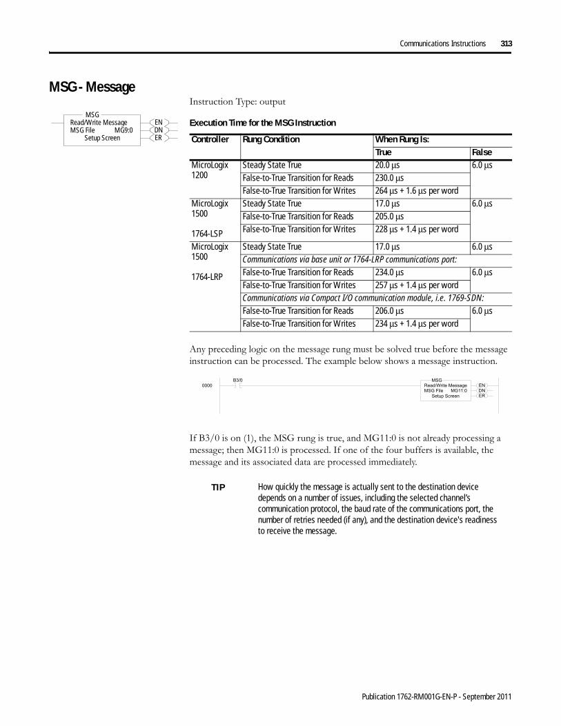
Communications Instructions 313
MSG - MessageInstruction Type: output
Any preceding logic on the message rung must be solved true before the message instruction can be processed. The example below shows a message instruction.
If B3/0 is on (1), the MSG rung is true, and MG11:0 is not already processing a message; then MG11:0 is processed. If one of the four buffers is available, the message and its associated data are processed immediately.
ENDNER
MSGRead/Write MessageMSG File MG9:0
Setup Screen
MSGExecution Time for the MSG Instruction
Controller Rung Condition When Rung Is:True False
MicroLogix 1200
Steady State True 20.0 μs 6.0 μsFalse-to-True Transition for Reads 230.0 μsFalse-to-True Transition for Writes 264 μs + 1.6 μs per word
MicroLogix 1500
1764-LSP
Steady State True 17.0 μs 6.0 μsFalse-to-True Transition for Reads 205.0 μsFalse-to-True Transition for Writes 228 μs + 1.4 μs per word
MicroLogix 1500
1764-LRP
Steady State True 17.0 μs 6.0 μsCommunications via base unit or 1764-LRP communications port:False-to-True Transition for Reads 234.0 μs 6.0 μsFalse-to-True Transition for Writes 257 μs + 1.4 μs per wordCommunications via Compact I/O communication module, i.e. 1769-SDN:False-to-True Transition for Reads 206.0 μs 6.0 μsFalse-to-True Transition for Writes 234 μs + 1.4 μs per word
TIP How quickly the message is actually sent to the destination device depends on a number of issues, including the selected channel’s communication protocol, the baud rate of the communications port, the number of retries needed (if any), and the destination device's readiness to receive the message.
Publication 1762-RM001G-EN-P - September 2011

314 Communications Instructions
The Message ElementThe MSG instruction built into the controller uses a MG data file to process the message instruction. The MG data file, shown at left, is accessed using the MG prefix. Each message instruction utilizes an element within a MG data file. For example, MG11:0 is the first element in message data file 11.
Message File Sub-Elements
Each MSG instruction must use a unique Element in a MSG File. The MSG element for each MSG instruction holds all of the parameters and status information for that particular MSG instruction.
Each MSG File Element consists of Sub-Elements 0 through 24 as shown in the following table.
Message File ElementSub-Element
Name Description Parameter Size User ProgramAccess(1)
0 to 1 Reserved Word read only
2 Messaging Type: 0 (for PCCC), 1 (for CIP), 2 (for Modbus Master) Word read only
3 for PCCC Messaging: bits 07-00 (CMD code), bits 15-08 (FNC code)
for CIP Messaging: bits 07-00 (Service Code), bits 15-08 (Supplemental Object Path Data Count)
for Modbus Master: bits 07-00 (Function Code), bits 15-08 (reserved)
derived Word read only
4 Internal Physical Address Word read only
5 MG11:0.RBL PCCC: Remote Bridge Link ID
CIP: Supplemental Object Path Data bytes 0 and 1
Modbus Master: not used
Y Word read only
6 MG11:0.LBN PCCC: Local Bridge Node Address
CIP: Supplemental Object Path Data bytes 2 and 3
Modbus Master: not used
Y Word read only
7 MG11:0.RBN PCCC: Remote Bridge Node Address
CIP: Supplemental Object Path Data bytes 4 and 5
Modbus Master: not used
Y Word read only
8 MG11:0.CHN Channel: bits 07-00 (0 for Channel 0,1 for Channel 1)
Slot: bits 15-08 (0 to 16)
Y Word read/write
9 MG11:0.NOD Target Node Number Y Word read/write
10 MG11:0.MTO Message timeout setting or preset in seconds Y Word read/write
Publication 1762-RM001G-EN-P - September 2011
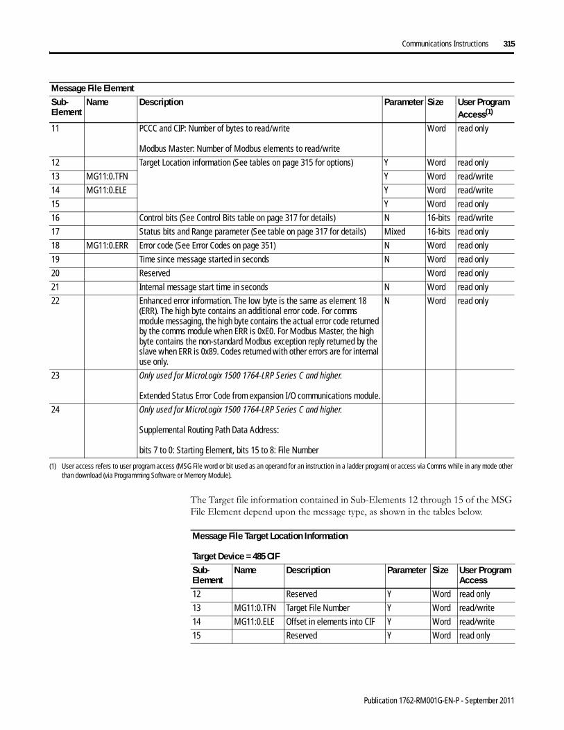
Communications Instructions 315
The Target file information contained in Sub-Elements 12 through 15 of the MSG File Element depend upon the message type, as shown in the tables below.
11 PCCC and CIP: Number of bytes to read/write
Modbus Master: Number of Modbus elements to read/write
Word read only
12 Target Location information (See tables on page 315 for options) Y Word read only
13 MG11:0.TFN Y Word read/write
14 MG11:0.ELE Y Word read/write
15 Y Word read only
16 Control bits (See Control Bits table on page 317 for details) N 16-bits read/write
17 Status bits and Range parameter (See table on page 317 for details) Mixed 16-bits read only
18 MG11:0.ERR Error code (See Error Codes on page 351) N Word read only
19 Time since message started in seconds N Word read only
20 Reserved Word read only
21 Internal message start time in seconds N Word read only
22 Enhanced error information. The low byte is the same as element 18 (ERR). The high byte contains an additional error code. For comms module messaging, the high byte contains the actual error code returned by the comms module when ERR is 0xE0. For Modbus Master, the high byte contains the non-standard Modbus exception reply returned by the slave when ERR is 0x89. Codes returned with other errors are for internal use only.
N Word read only
23 Only used for MicroLogix 1500 1764-LRP Series C and higher.
Extended Status Error Code from expansion I/O communications module.
24 Only used for MicroLogix 1500 1764-LRP Series C and higher.
Supplemental Routing Path Data Address:
bits 7 to 0: Starting Element, bits 15 to 8: File Number
(1) User access refers to user program access (MSG File word or bit used as an operand for an instruction in a ladder program) or access via Comms while in any mode other than download (via Programming Software or Memory Module).
Message File ElementSub-Element
Name Description Parameter Size User ProgramAccess(1)
Message File Target Location Information
Target Device = 485 CIF Sub-Element
Name Description Parameter Size User Program Access
12 Reserved Y Word read only
13 MG11:0.TFN Target File Number Y Word read/write
14 MG11:0.ELE Offset in elements into CIF Y Word read/write
15 Reserved Y Word read only
Publication 1762-RM001G-EN-P - September 2011

316 Communications Instructions
Message File Target Location Information
Target Device = 500CPU or PLC 5Sub-Element
Address Description Parameter Size User Program Access
12 Target File Type Y Word read only
13 MG11:0.TFN Target File Number(1) Y Word read/write
14 MG11:0.ELE Target File Element Number for B, S, N, F(2), T, C, R, L, ST and RTC(3) files; or Target File Slot Number for O and I files.
Y Word read/write
15 Target File Element Number for O and I files.
Set to zero for any file other than O or I.
Y Word read only
(1) The file number for RTC function files is set to 0 by the programming software.
(2) The F file is only permitted in the MSG instruction for MicroLogix 1200 and 1500 Series C and higher controllers.
(3) RTC and ST are only permitted in the MSG instruction for MicroLogix 1200 and 1500 Series B and higher controllers.
Message File Target Location Information
Target Device = CIP Generic
MicroLogix 1500 1764-LRP Series C, FRN 6 and higher Processor only.Sub-Element
Name Description Parameter Size User Program Access
12 Target Class Y Word read only
13 MG11:0.TFN Target Instance Y Word read/write
14 MG11:0.ELE CIP Send Data Count Y Word read/write
15 Reserved Y Word read only
Message File Target Location Information
Target Device = Modbus Device
MicroLogix 1500 1764-LRP Series C, FRN 9 and higher Processor only.Sub-Element
Name Description Parameter Size User Program Access
12 starting bit address for coils and inputs
Y Word read only
13 MG11:0.TFN Modbus Target Data Address - 1
Y Word read/write
14 Reserved Y Word read/write
15 Reserved Y Word read only
Publication 1762-RM001G-EN-P - September 2011

Communications Instructions 317
The Control Bits, Sub-Element 16, of the MSG File Element are defined below:
The Status Bits, Sub-Element 17, of the MSG File Element are defined below.
Message File Sub-Element 16 - Control BitsBit Address Description Parameter Size User Program
Access15 MG11:0.0/EN Enable
1=MSG enabled
0=MSG not enabled
N bit read/write
9 to 14 Reserved N bit read/write
8 MG11:0.0/TO Time Out
1=MSG time out by user
0=no user MSG time out
N bit read/write
0 to 7 Reserved N bit read/write
Message File Sub-Element 17 - Status BitsBit Address Description Parameter Size User
Program
Access15 Reserved N bit read only
14 MG11:0.0/ST Start:
1 = MSG transmitted and acknowledged by target device
0 = MSG has not been received by target
N bit read only
13 MG11:0.0/DN Done
1 = MSG completed successfully
0 = MSG not complete
N bit read only
12 MG11:0.0/ER Error
1 = error detected
0 = no error detected
N bit read only
11 Reserved N bit read only
10 MG11:0.0/EW Enabled and Waiting:
1=MSG Enabled and Waiting
0=MSG not Enabled and Waiting
N bit read only
Publication 1762-RM001G-EN-P - September 2011

318 Communications Instructions
“Control Bits” Parameters
Ignore if Timed Out (TO)
The Timed Out Bit (TO) can be set in your application to remove an active message instruction from processor control. You can create your own timeout routine by monitoring the EW and ST bits to start a timer. When the timer times out, you can set the TO bit, which removes the message from the system. The controller resets the TO bit the next time the associated MSG rung goes from false to true.
1 to 9 Reserved N bit read only
0 MG11:0.0/R For PCCC Messaging: Range (1 = Local, 0 = Remote)
For CIP Messaging: Target (1 = Comms Module, 0 = Network Device)
For Modbus Messaging: Range (1 = Local)
Y bit read only
Address Data Format Range Type User Program AccessMG11:0/TO Binary On or Off Control Read / Write
Message File Sub-Element 17 - Status BitsBit Address Description Parameter Size User
Program
Access
Publication 1762-RM001G-EN-P - September 2011

Communications Instructions 319
An easier method is to use the message timeout variable described on page 331, because it simplifies the user program. This built-in timeout control is in effect whenever the message timeout is non-zero. It defaults to 5 seconds, so unless you change it, the internal timeout control is automatically enabled.
When the internal timeout is used and communications are interrupted, the MSG instruction will timeout and error after the set period of time expires. This allows the control program to retry the same message or take other action, if desired.
To disable the internal timeout control, enter zero for the MSG instruction timeout parameter. If communications are interrupted, the processor waits indefinitely for a reply. If an acknowledge (ACK) is received, indicated by the ST bit being set, but the reply is not received, the MSG instruction appears to be locked up, although it is actually waiting for a reply from the target device.
Enable (EN)
The Enable Bit (EN) is set when rung conditions go true and the MSG is enabled. The MSG is enabled when the command packet is built and put into one of the MSG buffers, or the request is put in the MSG queue. It remains set until the message transmission is completed and the rung goes false. You may clear this bit when either the ER or DN bit is set in order to re-trigger a MSG instruction with true rung conditions on the next scan.
Enabled and Waiting (EW)
The Enabled and Waiting Bit (EW) is set after the enable bit is set and the message is in the buffer (not in the queue) and waiting to be sent. The EW bit is cleared after the message has been sent and the processor receives acknowledgement (ACK) from the target device. This is before the target device has processed the message and sent a reply.
Error (ER)
Address Data Format Range Type User Program AccessMG11:0/EN Binary On or Off Control Read / Write
IMPORTANT Do not set this bit from the control program.
Address Data Format Range Type User Program AccessMG11:0/EW Binary On or Off Status Read Only
Address Data Format Range Type User Program AccessMG11:0/ER Binary On or Off Status Read Only
Publication 1762-RM001G-EN-P - September 2011

320 Communications Instructions
The Error Bit (ER) is set when message transmission has failed. An error code is written to the MSG File. The ER bit and the error code are cleared the next time the associated rung goes from false to true.
Done (DN)
The Done Bit (DN) is set when the message is transmitted successfully. The DN bit is cleared the next time the associated rung goes from false to true.
Start (ST)
The Start Bit (ST) is set when the processor receives acknowledgment (ACK) from the target device. The ST bit is cleared when the DN, ER, or TO bit is set.
The DF1 Radio Modem and Modbus RTU Master protocols do not have acknowledgements. When the channel that the MSG instruction is being initiated on is configured for either of these two drivers, the Start Bit (ST) is set when the message has been successfully transmitted.
Timing Diagram for the MSG Instruction
The following section describes the timing diagram for a message instruction.
Address Data Format Range Type User Program AccessMG11:0/DN Binary On or Off Status Read Only
Address Data Format Range Type User Program AccessMG11:0/ST Binary On or Off Status Read Only
EN
EW
ST
DN
ER
TO
10
10
10
10
10
10
(1) Rung goes true.(3) Target node receives packet.
(5) Target node processes packet successfully and returns data (read) or acknowledges receipt (write).(1) (2) (3) (5) (6)
Publication 1762-RM001G-EN-P - September 2011

Communications Instructions 321
1. If there is room in any of the four active message buffers when the MSG rung becomes true and the MSG is scanned, the EN and EW bits for this message are set. If this is a MSG write instruction, the source data is transferred to the message buffer at this time.
(Not shown in the diagram.) If the four message buffers are in use, the message request is put in the message queue and only the EN bit is set. The message queue works on a first-in, first-out basis that allows the controller to remember the order in which the message instructions were enabled. When a buffer becomes available, the first message in the queue is placed into the buffer and the EW bit is set (1).
Once the EN bit is set (1), it remains set until the entire message process is complete and either the DN, ER, or TO bit is set (1). The MSG Timeout period begins timing when the EN bit is set (1). If the timeout period expires before the MSG instruction completes its function, the ER bit is set (1), and an error code (37H) is placed in the MG File to inform you of the timeout error.
2. At the next end of scan, REF, or SVC instruction, the controller determines if it should examine the communications queue for another instruction. The controller bases its decision on the state of the channel’s Communication Servicing Selection (CSS) and Message Servicing Selection (MSS) bits, the network communication requests from other nodes, and whether previous message instructions are already in progress. If the controller determines that it should not access the queue, the message instruction remains as it was. Either the EN and EW bits remain set (1) or only the EN bit is set (1) until the next end of scan, REF, or SVC instruction.
If the controller determines that it has an instruction in the queue, it unloads the communications queue entries into the message buffers until all four message buffers are full. If an invalid message is unloaded from the communications queue, the ER bit in the MG file is set (1), and a code is placed in the MG file to inform you of an error. When a valid message instruction is loaded into a message buffer, the EN and EW bits for this message are set (1).
The controller then exits the end of scan, REF, or SVC portion of the scan. The controller’s background communication function sends the messages to the target nodes specified in the message instruction. Depending on the state of the CSS and MSS bits, you can service up to four active message instructions per channel at any given time.
3. If the target node successfully receives the message, it sends back an acknowledge (ACK). The ACK causes the processor to clear (0) the EW bit and set (1) the ST bit. The target node has not yet examined the packet to see if it understands your request.
TIP The control program does not have access to the message buffers or the communications queue.
Publication 1762-RM001G-EN-P - September 2011

322 Communications Instructions
Once the ST bit is set (1), the controller waits for a reply from the target node. The target node is not required to respond within any given time frame.
4. Step 4 is not shown in the timing diagram. If you do not receive an ACK, step 3 does not occur. Instead, either no response or a negative acknowledge (NAK) is received. When this happens, the ST bit remains clear (0).
No response may be caused by:
• the target node is not there• the message became corrupted in transmission• the response was corrupted in response transmission
A NAK may be caused by:
• target node is busy • target node received a corrupt message• the message is too large
When a NAK occurs, the EW bit is cleared (0), and the ER bit is set (1), indicating that the message instruction failed.
5. Following the successful receipt of the packet, the target node sends a reply packet. The reply packet contains one of the following responses:• successful write request.• successful read request with data• failure with error code
At the next end of scan, REF, or SVC instruction, following the target node’s reply, the controller examines the message from the target device. If the reply is successful, the DN bit is set (1), and the ST bit is cleared (0). If it is a successful read request, the data is written to the data table. The message instruction function is complete.
If the reply is a failure with an error code, the ER bit is set (1), and the ST bit is cleared (0). The message instruction function is complete.
6. If the DN or ER bit is set (1) and the MSG rung is false, the EN bit is cleared (0) the next time the message instruction is scanned.
See MSG Instruction Ladder Logic on page 323 for examples using the message instruction.
TIP If the Target Node faults or power cycles during the message transaction, you will never receive a reply. This is why you should use a Message Timeout value in your MSG instruction.
Publication 1762-RM001G-EN-P - September 2011

Communications Instructions 323
MSG Instruction Ladder Logic
Enabling the MSG Instruction for Continuous Operation
The message instruction is enabled during the initial processor program scan and each time the message completes. For example, when the DN or ER bit is set.
Enabling the MSG Instruction Via User Supplied Input
This is an example of controlling when the message instruction operates. Input I:1/0 could be any user-supplied bit to control when messages are sent. Whenever I:1/0 is set and message MG11:0 is not enabled, the message instruction on rung 0001 is enabled.
0000 ENDNER
MSGRead/Write MessageMSG File MG11:0
Setup Screen
MSG
0001MG11:0
DN
MG11:0
ER
UMG11:0
EN
0002 END
Message Done Bit
Message Error Bit
Message Enable Bit
0000I:1
0
MG11:0
EN L
B3:0
0
0001B3:0
0ENDNER
MSGRead/Write MessageMSG File MG11:0
Setup Screen
MSG
0002MG11:0
DN
MG11:0
ER
UB3:0
0
0003 END
Message Done Bit
Message Error Bit
The message instruction is enabled with eachfalse-to-true transition of bit B3:0/0
User SuppliedInput
MessageEnable Bit
Publication 1762-RM001G-EN-P - September 2011

324 Communications Instructions
Local Messages The controller is capable of communicating using local or remote messages. With a local message, all devices are accessible without a separate device acting as a bridge. Different types of electrical interfaces may be required to connect to the network, but the network is still classified as a local network. Remote messages use a remote network, where devices are accessible only by passing or routing through a device to another network. Remote networks are discussed on page 346.
Local Networks
The following three examples represent different types of local networks.
Example 1 - Local DH-485 Network with AIC+ (1761-NET-AIC) Interface
Example 2 - Local DeviceNet Network with DeviceNet Interface (1761-NET-DNI)
A-B PanelViewTERM
A
B
COM
SHLD
CHS GND
TX
TX PWR
TX
DC SOURCE
CABLE
EXTERNAL
TERM
A
B
COM
SHLD
CHS GND
TX
TX PWR
TX
DC SOURCE
CABLE
EXTERNAL
TERM
A
B
COM
SHLD
CHS GND
TX
TX PWR
TX
DC SOURCE
CABLE
EXTERNAL
TERM
A
B
COM
SHLD
CHS GND
TX
TX PWR
TX
DC SOURCE
CABLE
EXTERNAL
TERM
A
B
COM
SHLD
CHS GND
TX
TX PWR
TX
DC SOURCE
CABLE
EXTERNAL
TERM
A
B
COM
SHLD
CHS GND
TX
TX PWR
TX
DC SOURCE
CABLE
EXTERNAL
AIC+ AIC+ AIC+
AIC+
DH-485 NetworkSLC 5/04 PanelView 550
MicroLogix 1500MicroLogix 1000 MicroLogix 1200
Personal Computer
AIC+
AIC+
DANGER
DANGER DANGER DANGER DANGER
DANGER
A-B PanelView
DNI DNI DNI
DNI
DeviceNet NetworkMaster
PanelView 550
MicroLogix 1500MicroLogix 1000 MicroLogix 1200
Personal Computer
DNI
DNI
SLC 5/03 with 1747-SDN
Publication 1762-RM001G-EN-P - September 2011

Communications Instructions 325
Example 3 - Local DF1 Half-Duplex Network
Configuring a Local Message
Message Setup Screen
The rung below shows a MSG instruction preceded by conditional logic. Access the message setup screen by double-clicking Setup Screen.
Rockwell Software RSLinx 2.0 (or higher), SLC 5/03, SLC 5/04, and SLC 5/05, or PLC-5 processors configured for DF1 Half-Duplex Master.
RS-232
MicroLogix1500 (Slave) SLC 5/04 (Slave)
MicroLogix1000 (Slave) SLC 5/03 with 1747-KE
Interface Module (Slave)
MicroLogix1200 (Slave)
Modem
TIP It is recommended that isolation (1761-NET-AIC) be provided between the controller and the modem.
0000B3:0
0ENDNER
MSGRead/Write MessageMSG File MG11:0
Setup Screen
MSG
Publication 1762-RM001G-EN-P - September 2011
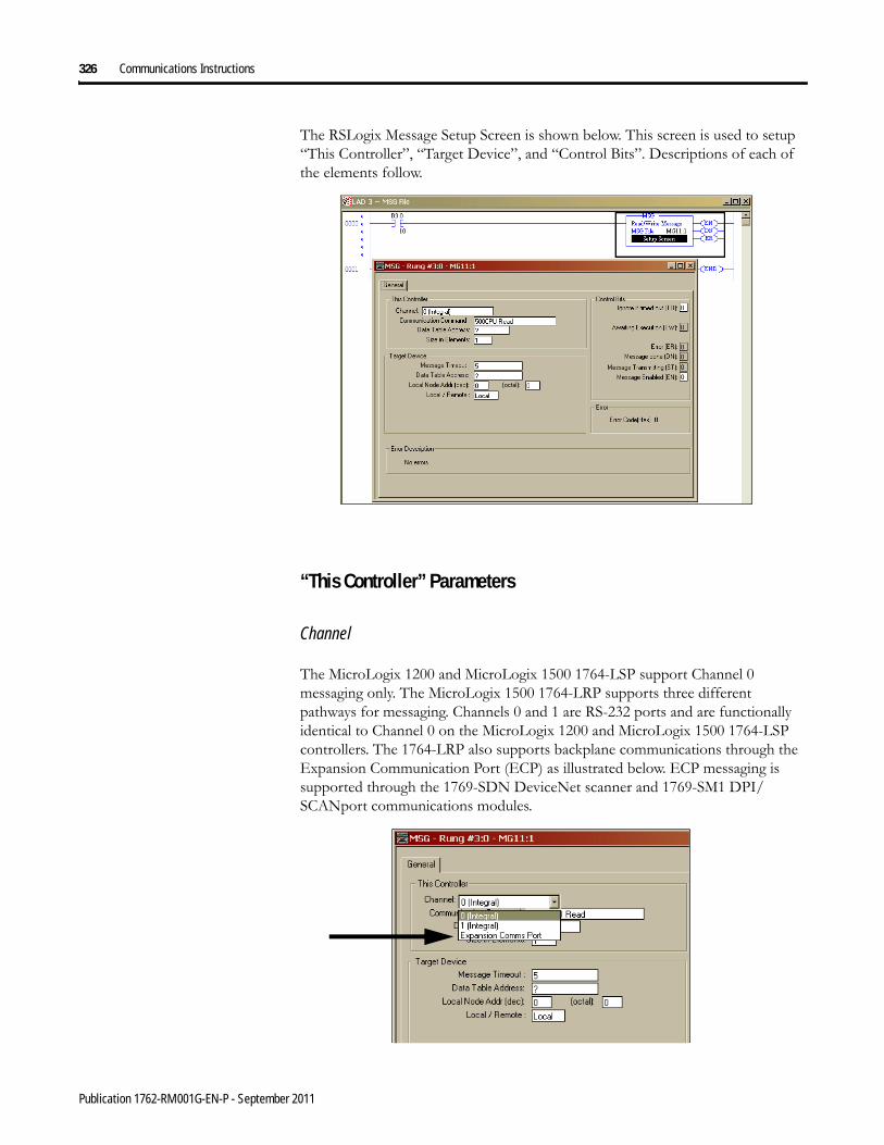
326 Communications Instructions
The RSLogix Message Setup Screen is shown below. This screen is used to setup “This Controller”, “Target Device”, and “Control Bits”. Descriptions of each of the elements follow.
“This Controller” Parameters
Channel
The MicroLogix 1200 and MicroLogix 1500 1764-LSP support Channel 0 messaging only. The MicroLogix 1500 1764-LRP supports three different pathways for messaging. Channels 0 and 1 are RS-232 ports and are functionally identical to Channel 0 on the MicroLogix 1200 and MicroLogix 1500 1764-LSP controllers. The 1764-LRP also supports backplane communications through the Expansion Communication Port (ECP) as illustrated below. ECP messaging is supported through the 1769-SDN DeviceNet scanner and 1769-SM1 DPI/SCANport communications modules.
Publication 1762-RM001G-EN-P - September 2011
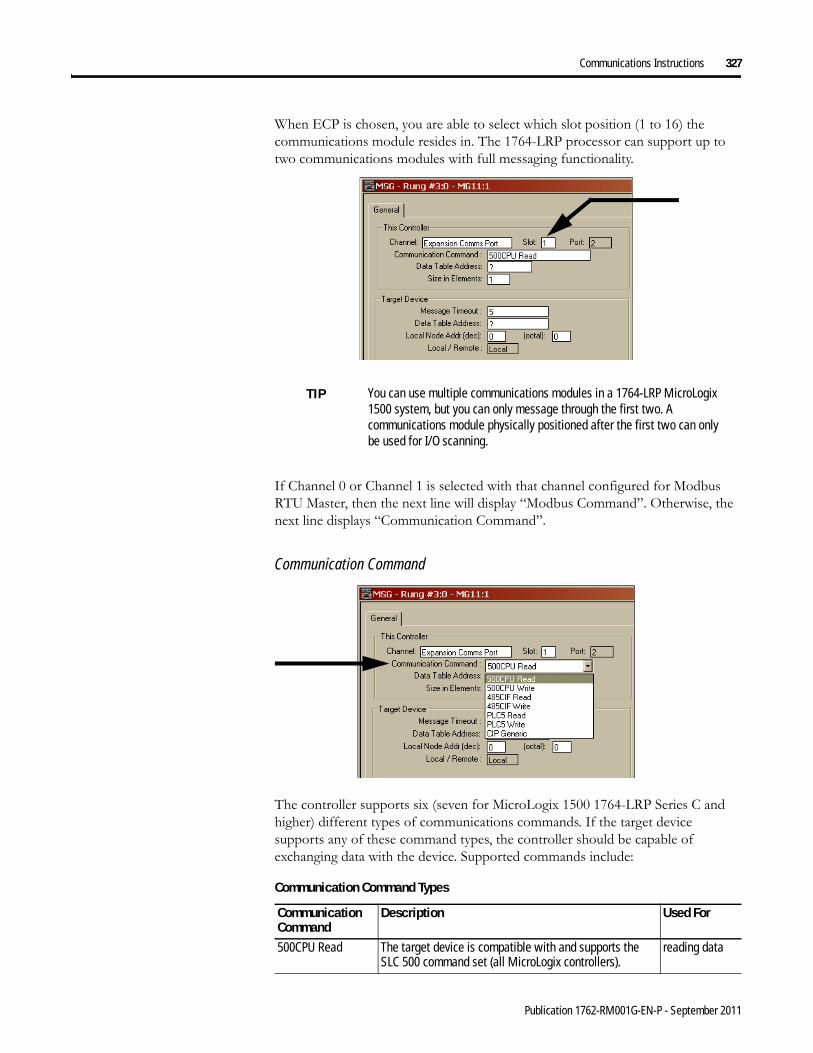
Communications Instructions 327
When ECP is chosen, you are able to select which slot position (1 to 16) the communications module resides in. The 1764-LRP processor can support up to two communications modules with full messaging functionality.
If Channel 0 or Channel 1 is selected with that channel configured for Modbus RTU Master, then the next line will display “Modbus Command”. Otherwise, the next line displays “Communication Command”.
Communication Command
The controller supports six (seven for MicroLogix 1500 1764-LRP Series C and higher) different types of communications commands. If the target device supports any of these command types, the controller should be capable of exchanging data with the device. Supported commands include:
TIP You can use multiple communications modules in a 1764-LRP MicroLogix 1500 system, but you can only message through the first two. A communications module physically positioned after the first two can only be used for I/O scanning.
Communication Command Types
Communication Command
Description Used For
500CPU Read The target device is compatible with and supports the SLC 500 command set (all MicroLogix controllers).
reading data
Publication 1762-RM001G-EN-P - September 2011

328 Communications Instructions
Modbus Command
500CPU Write The target device is compatible with and supports the SLC 500 command set (all MicroLogix controllers).
sending data
485CIF Read(1) The target device is compatible with and supports the 485CIF (PLC2).
reading data
485CIF Write(1) The target device is compatible with and supports the 485CIF (PLC2).
sending data
PLC5 Read The target device is compatible with and supports the PLC5 command set.
reading data
PLC5 Write The target device is compatible with and supports the PLC5 command set.
sending data
CIP Generic(2) The target device is compatible with and supports the CIP command set on DeviceNet (1769-SDN) or DPI/SCANport (1769-SM1).
Sending and receiving data
(1) See Important note below.
(2) MicroLogix 1500 1764-LRP Series C, FRN 6 and higher for DeviceNet messaging and DPI/SCANport messaging.
IMPORTANT The Common Interface File (CIF) in the MicroLogix 1200, 1500, and SLC 500 processors is File 9. The CIF in the MicroLogix 1000 controller is Integer File 7.
Communication Command Types
Communication Command
Description Used For
Publication 1762-RM001G-EN-P - September 2011

Communications Instructions 329
The controller supports eight Modbus commands. If the target device supports any of these Modbus command types, the controller should be capable of exchanging data with the device. Supported Modbus commands include:
Data Table Address
This variable defines the starting address in the local controller. Valid file types for the Data Table Address are shown below:
Modbus(1) Command Types
(1) MicroLogix 1200 Series C, FRN 8 and higher; and MicroLogix 1500 Series C, FRN 9 and higher.
Modbus Command Used For01 Read Coil Status reading bits
02 Read Input Status reading bits
03 Read Holding Registers reading words
04 Read Input Registers reading words
05 Write Single Coil writing 1 bit
06 Write Single Register writing 1 word
15 Write Multiple Coil writing multiple bits
16 Write Multiple Registers writing multiple words
Message Read Message WriteBit (B)
Timer (T)
Counter (C)
Control (R)
Integer (N)
Floating Point (F)(1)
Long Word (L)
(1) Applies to MicroLogix 1200 Series C and later, and 1500 Series C and later only. Message Type must be 500CPU or PLC5. The Local File Type and Target File Type must both be Floating Point.
Output (O)
Input (I)
Bit (B)
Timer (T)
Counter (C)
Control (R)
Integer (N)
Floating Point (F)(1)
Long Word (L)
String (ST)(2)(3)
Real-Time Clock (RTC)(2)(4)
(2) Applies to MicroLogix 1200 Series B and later, and 1500 Series B and later only.
(3) 485CIF write ST-to-485CIF only.
(4) 500CPU write RTC-to-Integer or RTC-to-RTC only.
Publication 1762-RM001G-EN-P - September 2011

330 Communications Instructions
Size in Elements
This variable defines the amount of data (in elements) to exchange with the target device.
The maximum amount of data that can be transferred via a MSG instruction is 103 words (120 words for Modbus commands) and is determined by the destination data type. The destination data type is defined by the type of message: read or write.
• For Read Messages: When a read message is used, the destination file is the data file in the local or originating processor.
• For Write Messages: When a write message is used, the destination file is the data file in the target processor.
The maximum number of elements that can be transmitted or received are shown in the following table. You cannot cross file types when sending messages. For example, you cannot read a timer into an integer file and you cannot write counters to a timer file. The only exceptions to this rule are that:
• long integer data can be read from or written to bit or integer files, and• RTC files can be written to integer files (MicroLogix 1200 Series B and later, and
1500 Series B and later only).
TIP Only Bit (B) and Integer (N) file types are valid for Modbus Command messages. Modbus bit commands require a starting bit address for the Data Table Address.
TIP Input, output, string, and RTC file types are not valid for read messages.
TIP The table below is not intended to illustrate file compatibility, only the maximum number of elements that can be exchanged in each case.
Message Type File Type Element Size Maximum Number of Elements per Message
485CIF O, I, B, N 1-word 103
L 2-word 51
T, C, R 3-word 34
ST 42-word 2 (write only)
500CPU O, I, B, N 1-word 103
F(1), L 2-word 51
T, C, R 3-word 34
RTC 8-word 1 (write only)
PLC5 O, I, B, N 1-word 103
F(1), L 2-word 51
T 5-word 20
Publication 1762-RM001G-EN-P - September 2011

Communications Instructions 331
“Target Device” Parameters
Message Timeout
This value defines how long, in seconds, the message instruction has to complete its operation once it has started. Timing begins when the false-to-true rung transition occurs, enabling the message. If the timeout period expires, the message errors out. The default value is 5 seconds (2 seconds for Modbus commands). The maximum timeout value is 255 seconds.
If the message timeout is set to zero, the message instruction will never timeout. Set the Time Out bit (TO = 1) to flush a message instruction from its buffer if the destination device does not respond to the communications request.
CIP B, N 1-word 126
F, L 2-words 63
Modbus Commands(2)
B, N (command 5) 1-bit 1
B, N (command 6) 1-word 1
B, N(commands 1, 2, and 15)
1-bit 1920 Modbus bit elements (120 words)(Commands 1 and 2 are read only, 15 is write only.)
B, N(commands 3, 4, and 16)
multi-register 120 Modbus register elements (120 words)(Commands 3 and 4 are read only, 16 is write only.)
(1) Applies to MicroLogix 1200 Series C and later, and 1500 Series C and later only. Message Type must be 500CPU or PLC5. The Local File Type and Target File Type must both be Floating Point.
(2) MicroLogix 1200 Series C, FRN 8 and higher; MicroLogix 1500 Series C, FRN 9 and higher.
Message Type File Type Element Size Maximum Number of Elements per Message
Publication 1762-RM001G-EN-P - September 2011

332 Communications Instructions
Data Table Address/Offset
This variable defines the starting address in the target controller. The data table address is used for a 500CPU and PLC5 type messages. A valid address is any valid, configured data file within the target device whose file type is recognized by the controller. Valid combinations are shown below:
The data table offset is used for 485CIF type messages. A valid offset is any value in the range 0 to 255 and indicates the word or byte offset into the target's Common Interface File (CIF). The type of device determines whether it is a word or byte offset. MicroLogix controllers and SLC processors use word offset; PLC-5 and ControlLogix processors use byte offset.
Modbus - MB Data Address (1-65536)
Modbus addressing is limited to 16 bits per memory group, each with a range of 1 to 65,536. There are four memory groups, one for each function:
• coils (generally addressed as 0xxxx)• contacts (1xxxx)• input registers (3xxxx)• holding registers (4xxxx)
Coils and contacts are addressed at the bit level. Coils are outputs and can be read and written. Contacts are inputs and are read-only.
Input registers and holding registers are addressed at the word level. Input registers are generally used for internally storing input values. They are read-only. Holding registers are general purpose and can be both read and written.
The most significant digit of the address is considered a prefix, and does not get entered into the MB Data Address field when configuring the message instruction.
Message Type Local File Type Target File Type500CPU and PLC5 O, I, B, N, F(1), L
(1) Applies to MicroLogix 1200 Series C and later, and 1500 Series C and later only. Message Type must be 500CPU or PLC5. The Local File Type and Target File Type must both be Floating Point.
O, I, S, B, N, F(1), L
T T
C C
R R
RTC(2)
(2) 500CPU write RTC-to-Integer or RTC-to-RTC only. Applies to MicroLogix 1200 Series B and later, and 1500 Series B and later only.
N, RTC
Publication 1762-RM001G-EN-P - September 2011

Communications Instructions 333
When the message is sent, the address is decremented by 1 and converted into a 4-character hex number to be transmitted via the network (with a range of 0-FFFFh); the slave increments the address by 1, and selects the appropriate memory group based on the Modbus function.
Local/Slave Node Address
This is the destination device's node number if the devices are on a DH-485 (using 1761-NET-AIC), DeviceNet (using 1761-NET-DNI), DF1, or Modbus network.
Local/Remote
This variable defines the type of communications that is used. Always use local when you need point-to-point communications via DF1 Full-Duplex or network communications such as Ethernet/IP (using 1761-NET-ENI), DeviceNet (using 1761-NET-DNI), DF1 Half-Duplex, or DF1 Radio Modem. For DH-485, use local if the target node is on the same DH-485 network as this controller, or remote if the path to the target node goes through one or more communication bridges.
Local Messaging Examples
Five examples of local messaging are shown in this section:
• 500CPU message type• 485CIF message type• PLC5 message type• CIP Generic message type over DeviceNet via 1747-SDN• Modbus RTU Message type
TIP Modbus protocol may not be consistently implemented in all devices. The Modbus specification calls for the addressing range to start at 1; however, some devices start addressing at 0.
The Modbus Data Address in the Message Setup Screen may need to be incremented by one to properly access a Modbus slave’s memory, depending on that slave’s implementation of memory addressing.
TIP To initiate a broadcast message on a DH-485, DF1 Half-Duplex, or DF1 Radio Modem network, set the local node address to -1.
To initiate a broadcast message on a Modbus network, set the slave node address to 0. Do not initiate more than one Modbus broadcast message at a time. When sequentially triggering multiple Modbus broadcast messages, insert at least 10 msec. delay in between each message.
Publication 1762-RM001G-EN-P - September 2011

334 Communications Instructions
A summary of the message instruction configuration parameters is shown in the following table.
Parameter DescriptionThis Controller Channel Identifies the communication channel. Always Channel 0 (or Channel 1 or Expansion
Communications Port for MicroLogix 1500 1764-LRP Processor only.)Communication Command(500CPU, 485CIF, PLC5, and ECP message types)
Specifies the type of message. Valid types are:
• 500CPU Read
• 500CPU Write
• 485CIF Read
• 485CIF Write
• PLC5 Read
• PLC5 Write
• CIP GenericModbus Command Specifies the type of message. Valid types are:
• 01 Read Coil Status
• 02 Read Input Status
• 03 Read Holding Registers
• 04 Read Input Registers
• 05 Write Single Coil
• 06 Write Single Register
• 15 Write Multiple Coils
• 16 Write Multiple RegistersData Table Address For a Read, this is the starting address which receives data. Valid file types are B, T, C, R, N,
and L (for Modbus commands, B and N only).For a Write, this is the starting address which is sent to the target device. Valid file types are O, I, B, T, C, R, N, L, ST(1)(2), and RTC(2)(3) (for Modbus commands, B and N only).
Size in elements Defines the length of the message in elements.
• 1-word elements; valid size: 1 to 103.
• 2-word elements; valid size: 1 to 51.
• 8-word RTC elements; valid size: 1
• 42-word String elements; valid size 1 to 2
• Timer (500CPU and 485CIF), Counter, and Control elements; valid size: 1 to 34.
• PLC-5 Timer elements; valid size: 1 to 20
• Modbus bit elements: 1 to 1920
• Modbus register elements: 1 to 120
Publication 1762-RM001G-EN-P - September 2011

Communications Instructions 335
Example 1 - Local Read from a 500CPU
Message Instruction Setup
In this example, the controller reads 10 elements from the target’s (Local Node 2) N7 file, starting at word N7:50. The 10 words are placed in the controller’s integer file starting at word N7:0. If five seconds elapse before the message completes, error bit MG11:0/ER is set, indicating that the message timed out.
Target Device Message Timeout Defines the amount of time the controller waits for the reply before the message errors. A timeout of 0 seconds means that the controller waits indefinitely for a reply. Valid range is from 0 to 255 seconds.
Data Table Address (500CPU and PLC5 message types)
For a Read, this is the address in the processor which is to return data. Valid file types are S, B, T, C, R, N, and L.For a Write, this is the address in the processor which receives data. Valid file types are I, O, S, B, T, C, R, N, L, and RTC(2)(4).
Data Table Offset
(485CIF message types)
This is the word offset value in the common interface file (byte offset for PLC device) in the target processor, which is to send the data.
MB Data Address Specifies the Modbus address in the target device. Valid range is from 1 to 65,536.Local Slave Node Address
Specifies the node number of the device that is receiving the message. Valid range is 0 to 31 for DH-485 protocol, 0 to 254 for DF1 protocol, 0 to 63 for DeviceNet, or 0 to 247 for Modbus.
Local/Remote Specifies whether the message is local or remote. (Modbus messages are local only.)
(1) Applies to MicroLogix 1200 Series B and later, and 1500 Series B and later.
(2) 485CIF write ST-to-485CIF only.
(3) 500CPU write RTC-to-Integer or RTC-to-RTC only.
Parameter Description
Publication 1762-RM001G-EN-P - September 2011

336 Communications Instructions
Valid File Type Combinations
Valid transfers between file types are shown below for MicroLogix messaging:
Example 2 - Local Read from a 485CIF
Message Instruction Setup
In this example, the controller reads five elements (words) from the target device’s (Local Node 2) CIF file, starting at word 20 (or byte 20 for non-SLC 500 devices). The five elements are placed in the controller’s integer file starting at word N7:0. If 15 seconds elapse before the message completes, error bit MG11:0/ER is set, indicating that the message timed out.
Local Data Types Communication Type Target Data Types
O(1), I(1), B, N, L
(1) Output and input data types are not valid local data types for read messages.
<---> read/write O, I, S, B, N, L
T <---> read/write TC <---> read/write CR <---> read/write R
RTC(2)
(2) 500CPU write RTC-to-Integer or RTC-to-RTC only. Applies to MicroLogix 1200 Series B and later, and 1500 Series B and later only.
---> write N, RTC
Publication 1762-RM001G-EN-P - September 2011

Communications Instructions 337
Valid File Type Combinations
Valid transfers between file types are shown below for MicroLogix messaging:
Example 3 - Local Read from a PLC-5
Message Instruction Setup
In this example, the controller reads 10 elements from the target device’s (Local Node 2) N7 file, starting at word N7:50. The 10 words are placed in the controller’s integer file starting at word N7:0. If five seconds elapse before the message completes, error bit MG11:0/ER is set, indicating that the message timed out.
Local Data Types Communication Type Target Data Types
O(1), I(1), B, N, L
(1) Output and input data types are not valid local data types for read messages.
<---> read/write 485CIF
T <---> read/write 485CIFC <---> read/write 485CIFR <---> read/write 485CIF
ST(2)
(2) Applies to MicroLogix 1200 Series B and later, and 1500 Series B and later only.
---> write 485CIF
Publication 1762-RM001G-EN-P - September 2011

338 Communications Instructions
Valid File Type Combinations
Valid transfers between file types are shown below for MicroLogix messaging:
Example 4 - Configuring a Local DeviceNet Message
This section describes how to configure a local message using the scanner and a MicroLogix 1500 1764-LRP processor. An example network is shown below:
Local Data Types Communication Type Target Data Types
O(1), I(1), B, N, L
(1) Output and input data types are not valid local data types for read messages.
<---> read/write O, I, S, B, N, L
T <---> read/write TC <---> read/write CR <---> read/write R
DANGER DANGER
PC with RSNetWorxfor DeviceNet software
Series 9000Photoeye
RediSTATION
DeviceNet Network
1770-KFD PC Communication Module
MicroLogix 1500 Controller I/O Bank with 1769-SDN Module
MicroLogix 1000 Controller Connected via 1761-NET-DNI
MicroLogix 1200 Controller Connected via 1761-NET-DNI
1305 Drive Connected via 1203-GU6 Enhanced DeviceNet Communications Module
Publication 1762-RM001G-EN-P - September 2011
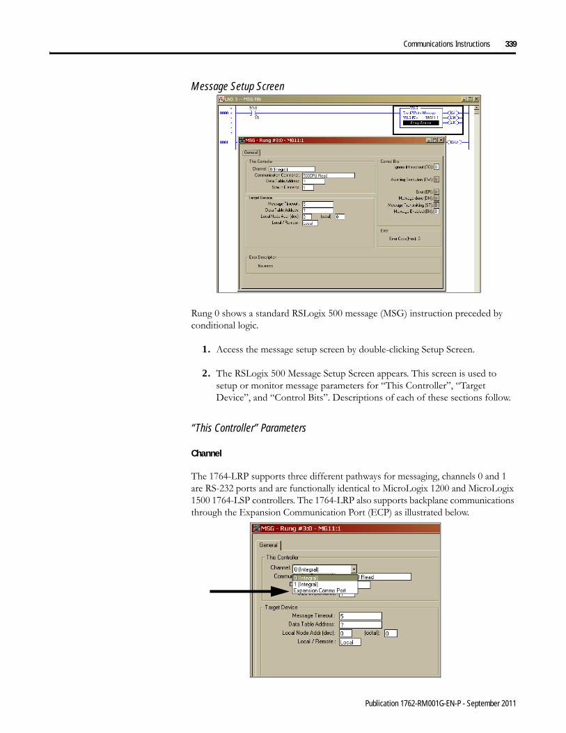
Communications Instructions 339
Message Setup Screen
Rung 0 shows a standard RSLogix 500 message (MSG) instruction preceded by conditional logic.
1. Access the message setup screen by double-clicking Setup Screen.
2. The RSLogix 500 Message Setup Screen appears. This screen is used to setup or monitor message parameters for “This Controller”, “Target Device”, and “Control Bits”. Descriptions of each of these sections follow.
“This Controller” Parameters
Channel
The 1764-LRP supports three different pathways for messaging, channels 0 and 1 are RS-232 ports and are functionally identical to MicroLogix 1200 and MicroLogix 1500 1764-LSP controllers. The 1764-LRP also supports backplane communications through the Expansion Communication Port (ECP) as illustrated below.
Publication 1762-RM001G-EN-P - September 2011

340 Communications Instructions
When ECP is chosen, you are able to select which slot position (1 to 16) the scanner resides in. The 1764-LRP processor can support up to two 1769-SDN scanner modules with full messaging functionality.
CIP Generic Communication Command
The 1764-LRP processor supports the six standard types of communications commands (same as all other MicroLogix 1200 and 1500 controllers) and CIP Generic on the Expansion Comms Port. When any of the six standard commands are chosen, you can initiate standard messages to destination devices connected to DeviceNet products that support PCCC messaging (including MicroLogix and SLC controllers using 1761-NET-DNI’s, 1203-GU6 drive interface, and other MicroLogix 1500 controllers using 1769-SDN scanner modules). You can initiate reads, writes, program upload/download and online monitoring across DeviceNet. This is functionally identical to DH-485 and DH+ networking.
TIP You can use multiple 1769-SDN scanner modules in a 1764-LRP MicroLogix 1500 system, but you can only message through the first two. A scanner physically positioned after the first two can only be used for I/O scanning.
Publication 1762-RM001G-EN-P - September 2011

Communications Instructions 341
CIP stands for “Common Industrial Protocol”. CIP is a newer and more versatile protocol than PCCC. It is an open protocol that is supported by newer Allen-Bradley controllers and third-party products.
CIP messaging is the native messaging format for DeviceNet. All DeviceNet devices are compliant with CIP messaging. The MicroLogix 1500 1764-LRP processor (Series C) has an enhanced message instruction that provides simple, easy to use CIP messaging.
Selecting CIP Generic configures the message instruction to communicate with DeviceNet devices that do not support PCCC messaging. When CIP Generic is chosen, you will notice that a number of message parameters change and many new ones become available depending upon the service selected.
Data Table Address (Receive and Send)
This value identifies the data file location within the 1764-LRP controller that will receive data from the DeviceNet device, and/or the starting data file location that will be sent to the destination DeviceNet device.
Publication 1762-RM001G-EN-P - September 2011

342 Communications Instructions
Size in Bytes (Receive and Send)
Since all data transmitted on DeviceNet is byte based, you must enter the number of bytes that will be received and sent. You must make sure that enough memory is available in the destination device. Word elements within 1764-LRP controllers contain 2 bytes each. These include Bit and Integer data files. Long word and Floating point elements contain 4 bytes each.
For receive, the Size in bytes entered must be greater than or equal to the number of bytes than the DeviceNet device will return. DeviceNet devices return a fixed number of bytes depending on the Class and Service. If more data is returned than expected, the message will error and no data will be written. If less data is returned than expected, the data will be written and the remainder of the bytes will be filled with zeros.
In the example screen shown below, N7:0 will receive 2 bytes (1 word) of data.
Target Device
Publication 1762-RM001G-EN-P - September 2011
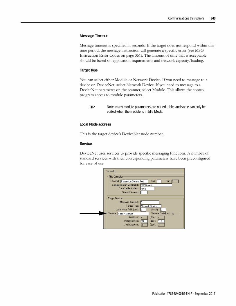
Communications Instructions 343
Message Timeout
Message timeout is specified in seconds. If the target does not respond within this time period, the message instruction will generate a specific error (see MSG Instruction Error Codes on page 351). The amount of time that is acceptable should be based on application requirements and network capacity/loading.
Target Type
You can select either Module or Network Device. If you need to message to a device on DeviceNet, select Network Device. If you need to message to a DeviceNet parameter on the scanner, select Module. This allows the control program access to module parameters.
Local Node address
This is the target device’s DeviceNet node number.
Service
DeviceNet uses services to provide specific messaging functions. A number of standard services with their corresponding parameters have been preconfigured for ease of use.
TIP Note, many module parameters are not editable, and some can only be edited when the module is in Idle Mode.
Publication 1762-RM001G-EN-P - September 2011

344 Communications Instructions
If you need to use a service that is not available, select one of the Generic services. The Generic service allows you to enter specific service code parameters. Information on what services a target device supports is usually provided in the device’s documentation.
Example 5 - Configuring a Modbus Message
This section describes how to configure a local message using the Modbus communication commands. Since configuration options are dependent on which channel is selected, the programming software has been designed to only show the options available for the selected channel.
Before configuring the MSG instruction, open the Channel Configuration screen and set the Driver to Modbus RTU Master. For more information on Channel Configuration, see Modbus RTU Master Configuration on page 449.
Publication 1762-RM001G-EN-P - September 2011
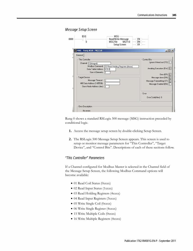
Communications Instructions 345
Message Setup Screen
Rung 0 shows a standard RSLogix 500 message (MSG) instruction preceded by conditional logic.
1. Access the message setup screen by double-clicking Setup Screen.
2. The RSLogix 500 Message Setup Screen appears. This screen is used to setup or monitor message parameters for “This Controller”, “Target Device”, and “Control Bits”. Descriptions of each of these sections follow.
“This Controller” Parameters
If a Channel configured for Modbus Master is selected in the Channel field of the Message Setup Screen, the following Modbus Command options will become available:
• 01 Read Coil Status (0xxxx)• 02 Read Input Status (1xxxx)• 03 Read Holding Registers (4xxxx)• 04 Read Input Registers (3xxxx)• 05 Write Single Coil (0xxxx)• 06 Write Single Register (4xxxx)• 15 Write Multiple Coils (0xxxx)• 16 Write Multiple Registers (4xxxx)
0000B3:0
0ENDNER
MSGRead/Write MessageMSG File MG11:0
Setup Screen
MSG
Publication 1762-RM001G-EN-P - September 2011

346 Communications Instructions
Data Table Address
Local file types must be Binary (B) or Integer (N) for Modbus commands. Starting data table address for coil/input bit commands (1, 2, 5 and 15) require a bit address. Starting data table addresses for register commands (3, 4, 6 and 16) require a word address.
Size in Elements
Size in elements defaults to “1”. For coil/input commands (1, 2, 5 and 15), elements are in bits. For register commands (3, 4, 6 and 10), elements are in words.
Target Device
Message Timeout
Message timeout is specified in seconds. If the target does not respond within this time period, the message instruction will generate a specific error (see MSG Instruction Error Codes on page 351). The amount of time that is acceptable should be based on application requirements and network capacity/loading. A 2-second message timeout is generally sufficient, as long as only one message is triggered at a time.
Modbus Data Address (decimal)
The default Modbus Data Address is 1. The Range is 1 to 65,536.
Slave Node Address (decimal)
The default Slave Node Address is 1. The Range is 0 to 247. Zero is the Modbus broadcast address and is only valid for Modbus write commands (5, 6, 15 and 16).
Remote Messages The controller is also capable of remote or off-link messaging. Remote messaging is the ability to exchange information with a device that is not connected to the local network. This type of connection requires a device on the local network to act as a bridge or gateway to the other network.
Remote Networks
DH-485 and DH+ Networks
The illustration below shows two networks, a DH-485 and a DH+ network. The SLC 5/04 processor at DH-485 node 17 is configured for passthru operation. Devices that are capable of remote messaging and are connected on either network can initiate read or write data exchanges with devices on the other network, based on each device's capabilities. In this example, node 12 on DH-485 is a MicroLogix
Publication 1762-RM001G-EN-P - September 2011
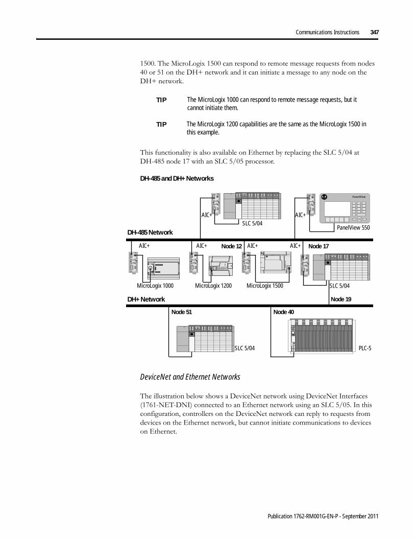
Communications Instructions 347
1500. The MicroLogix 1500 can respond to remote message requests from nodes 40 or 51 on the DH+ network and it can initiate a message to any node on the DH+ network.
This functionality is also available on Ethernet by replacing the SLC 5/04 at DH-485 node 17 with an SLC 5/05 processor.
DH-485 and DH+ Networks
DeviceNet and Ethernet Networks
The illustration below shows a DeviceNet network using DeviceNet Interfaces (1761-NET-DNI) connected to an Ethernet network using an SLC 5/05. In this configuration, controllers on the DeviceNet network can reply to requests from devices on the Ethernet network, but cannot initiate communications to devices on Ethernet.
TIP The MicroLogix 1000 can respond to remote message requests, but it cannot initiate them.
TIP The MicroLogix 1200 capabilities are the same as the MicroLogix 1500 in this example.
A-B PanelViewTERM
A
B
COM
SHLD
CHS GND
TX
TX PWR
TX
DC SOURCE
CABLE
EXTERNAL
TERM
A
B
COM
SHLD
CHS GND
TX
TX PWR
TX
DC SOURCE
CABLE
EXTERNAL
TERM
A
B
COM
SHLD
CHS GND
TX
TX PWR
TX
DC SOURCE
CABLE
EXTERNAL
TERM
A
B
COM
SHLD
CHS GND
TX
TX PWR
TX
DC SOURCE
CABLE
EXTERNAL
TERM
A
B
COM
SHLD
CHS GND
TX
TX PWR
TX
DC SOURCE
CABLE
EXTERNAL
TERM
A
B
COM
SHLD
CHS GND
TX
TX PWR
TX
DC SOURCE
CABLE
EXTERNAL
AIC+ AIC+ AIC+
AIC+
DH-485 NetworkSLC 5/04
PanelView 550
MicroLogix 1500MicroLogix 1000 MicroLogix 1200 SLC 5/04
AIC+
AIC+
SLC 5/04 PLC-5
DH+ Network
Node 17
Node 19
Node 51 Node 40
Node 12
Publication 1762-RM001G-EN-P - September 2011

348 Communications Instructions
DeviceNet and Ethernet Networks
Configuring a Remote Message
You configure for remote capability in the RSLogix 500 Message Setup screen.
Example Configuration Screen and Network
The message configuration shown below is for the MicroLogix 1500 at node 12 on the DH-485 network. This message reads five elements of data from the SLC 5/04 (node 51 on the DH+ network) starting at address N:50:0. The SLC 5/04 at Node 23 of the DH+ network is configured for passthru operation.
A-B PanelView
TERM
A
B
COM
SHLD
CHS GND
TX
TX PWR
TX
DC SOURCE
CABLE
EXTERNAL
TERM
A
B
COM
SHLD
CHS GND
TX
TX PWR
TX
DC SOURCE
CABLE
EXTERNAL
TERM
A
B
COM
SHLD
CHS GND
TX
TX PWR
TX
DC SOURCE
CABLE
EXTERNAL
TERM
A
B
COM
SHLD
CHS GND
TX
TX PWR
TX
DC SOURCE
CABLE
EXTERNAL
TERM
A
B
COM
SHLD
CHS GND
TX
TX PWR
TX
DC SOURCE
CABLE
EXTERNAL
TERM
A
B
COM
SHLD
CHS GND
TX
TX PWR
TX
DC SOURCE
CABLE
EXTERNAL
DNI DNI DNI
DNI
DeviceNet NetworkSLC 5/03
PanelView 550
MicroLogix 1500MicroLogix 1000 MicroLogix 1200 SLC 5/05
DNI
DNI
SLC 5/05 PLC-5E
Ethernet Network
TIP The MicroLogix 1200 capabilities are the same as the MicroLogix 1500 in this example.
Publication 1762-RM001G-EN-P - September 2011

Communications Instructions 349
DH-485 and DH+ Example Network
“This Controller” Parameters
See “Target Device” Parameters on page 331.
A-B PanelViewTERM
A
B
COM
SHLD
CHS GND
TX
TX PWR
TX
DC SOURCE
CABLE
EXTERNAL
TERM
A
B
COM
SHLD
CHS GND
TX
TX PWR
TX
DC SOURCE
CABLE
EXTERNAL
TERM
A
B
COM
SHLD
CHS GND
TX
TX PWR
TX
DC SOURCE
CABLE
EXTERNAL
TERM
A
B
COM
SHLD
CHS GND
TX
TX PWR
TX
DC SOURCE
CABLE
EXTERNAL
TERM
A
B
COM
SHLD
CHS GND
TX
TX PWR
TX
DC SOURCE
CABLE
EXTERNAL
TERM
A
B
COM
SHLD
CHS GND
TX
TX PWR
TX
DC SOURCE
CABLE
EXTERNAL
AIC+ AIC+ AIC+
AIC+
DH-485 NetworkSLC 5/03
PanelView 550
MicroLogix 1500MicroLogix 1000 MicroLogix 1200 SLC 5/04
AIC+
AIC+
SLC 5/04 PLC-5
DH+ Network
Node 17
Node 23 octal (19 decimal)
Node 63 octal (51 decimal) Node 40 octal (32 decimal)
Node 12
Node 5 Node 22
Node 11Node 10
Link ID = 100
Link ID = 1
Publication 1762-RM001G-EN-P - September 2011

350 Communications Instructions
“Control Bits” Parameters
See “Control Bits” Parameters on page 318.
“Target Device” Parameters
Message Timeout
See Message Timeout on page 331.
Data Table Address
See Data Table Address/Offset on page 332.
Local Bridge Address
This variable defines the bridge address on the local network. In the example, DH-485 node 12 (MicroLogix 1500 on Link ID 1) is writing data to node 51 (SLC 5/04 on Link ID 100). The SLC 5/04 at node 17 is the bridge device.
This variable sends the message to local node 17.
Remote Bridge Address
This variable defines the remote node address of the bridge device. In this example, the remote bridge address is set to zero, because the target device, SLC 5/04 at node 63 (octal) is a remote-capable device. If the target device is remote-capable, the remote bridge address is not required. If the target device is not remote-capable (SLC 500, SLC 5/01, SLC 5/02, and MicroLogix 1000 Series A, B and C), the remote bridge address is required.
Remote Station Address
This variable is the final destination address of the message instruction. In this example, integer file 50 elements 0 to 4 of the SLC 5/04 on Link ID 100 at node 63 (octal) receives data from the MicroLogix 1500 controller at node 12 on Link ID 1.
Publication 1762-RM001G-EN-P - September 2011
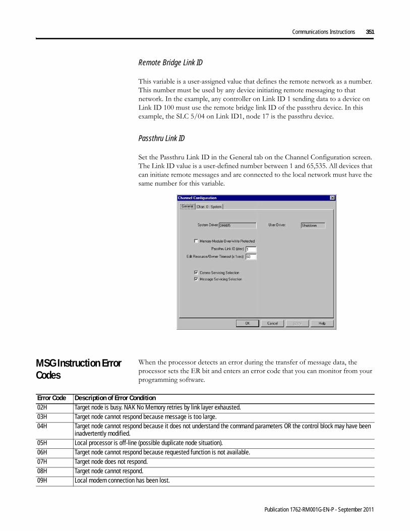
Communications Instructions 351
Remote Bridge Link ID
This variable is a user-assigned value that defines the remote network as a number. This number must be used by any device initiating remote messaging to that network. In the example, any controller on Link ID 1 sending data to a device on Link ID 100 must use the remote bridge link ID of the passthru device. In this example, the SLC 5/04 on Link ID1, node 17 is the passthru device.
Passthru Link ID
Set the Passthru Link ID in the General tab on the Channel Configuration screen. The Link ID value is a user-defined number between 1 and 65,535. All devices that can initiate remote messages and are connected to the local network must have the same number for this variable.
MSG Instruction Error Codes
When the processor detects an error during the transfer of message data, the processor sets the ER bit and enters an error code that you can monitor from your programming software.
Error Code Description of Error Condition02H Target node is busy. NAK No Memory retries by link layer exhausted.03H Target node cannot respond because message is too large.04H Target node cannot respond because it does not understand the command parameters OR the control block may have been
inadvertently modified.05H Local processor is off-line (possible duplicate node situation).06H Target node cannot respond because requested function is not available.07H Target node does not respond.08H Target node cannot respond.09H Local modem connection has been lost.
Publication 1762-RM001G-EN-P - September 2011

352 Communications Instructions
0BH Target node does not accept this type of MSG instruction.0CH Received a master link reset (one possible source is from the DF1 master).0FH DCOMM button was activated while an ASCII instruction was waiting to execute.10H Target node cannot respond because of incorrect command parameters or unsupported command.12H Local channel configuration protocol error exists.13H Local MSG configuration error in the Remote MSG parameters.15H Local channel configuration parameter error exists.16H Target or Local Bridge address is higher than the maximum node address.17H Local service is not supported.18H Broadcast is not supported.20H PCCC Description: Host has a problem and will not communicate.21H Bad MSG file parameter for building message.30H PCCC Description: Remote station host is not there, disconnected, or shutdown.37H Message timed out in local processor.39H Local communication channel reconfigured while MSG active.3AH STS in the reply from target is invalid.40H PCCC Description: Host could not complete function due to hardware fault.45H MSG reply cannot be processed. Either Insufficient data in MSG read reply or bad network address parameter. 50H Target node is out of memory.60H Target node cannot respond because file is protected.70H PCCC Description: Processor is in Program Mode.80H PCCC Description: Compatibility mode file missing or communication zone problem.81H Modbus Error 1: Illegal Function82H Modbus Error 2: Illegal Data Address83H Modbus Error 3: Illegal Data Value84H Modbus Error 4: Slave Device Failure85H Modbus Error 5: Acknowledge86H Modbus Error 6: Slave Device Busy87H Modbus Error 7: Negative Acknowledge88H Modbus Error 8: Memory Parity Error89H Modbus Error: Non-standard reply. Actual code returned can be found in the upper byte of sub-element 22.90H PCCC Description: Remote station cannot buffer command.B0H PCCC Description: Remote station problem due to download.C0H PCCC Description: Cannot execute command due to active IPBs.D0H One of the following:
• No IP address configured for the network.
• Bad command - unsolicited message error.
• Bad address - unsolicited message error.
• No privilege - unsolicited message error.D1H Maximum connections used - no connections available.D2H Invalid internet address or host name.D3H No such host / Cannot communicate with the name server.D4H Connection not completed before user–specified timeout.D5H Connection timed out by the network.
Error Code Description of Error Condition
Publication 1762-RM001G-EN-P - September 2011

Communications Instructions 353
0BH Target node does not accept this type of MSG instruction.0CH Received a master link reset (one possible source is from the DF1 master).0FH DCOMM button was activated while an ASCII instruction was waiting to execute.10H Target node cannot respond because of incorrect command parameters or unsupported command.12H Local channel configuration protocol error exists.13H Local MSG configuration error in the Remote MSG parameters.15H Local channel configuration parameter error exists.16H Target or Local Bridge address is higher than the maximum node address.17H Local service is not supported.18H Broadcast is not supported.20H PCCC Description: Host has a problem and will not communicate.21H Bad MSG file parameter for building message.30H PCCC Description: Remote station host is not there, disconnected, or shutdown.37H Message timed out in local processor.39H Local communication channel reconfigured while MSG active.3AH STS in the reply from target is invalid.40H PCCC Description: Host could not complete function due to hardware fault.45H MSG reply cannot be processed. Either Insufficient data in MSG read reply or bad network address parameter. 50H Target node is out of memory.60H Target node cannot respond because file is protected.70H PCCC Description: Processor is in Program Mode.80H PCCC Description: Compatibility mode file missing or communication zone problem.81H Modbus Error 1: Illegal Function82H Modbus Error 2: Illegal Data Address83H Modbus Error 3: Illegal Data Value84H Modbus Error 4: Slave Device Failure85H Modbus Error 5: Acknowledge86H Modbus Error 6: Slave Device Busy87H Modbus Error 7: Negative Acknowledge88H Modbus Error 8: Memory Parity Error89H Modbus Error: Non-standard reply. Actual code returned can be found in the upper byte of sub-element 22.90H PCCC Description: Remote station cannot buffer command.B0H PCCC Description: Remote station problem due to download.C0H PCCC Description: Cannot execute command due to active IPBs.D0H One of the following:
• No IP address configured for the network.
• Bad command - unsolicited message error.
• Bad address - unsolicited message error.
• No privilege - unsolicited message error.D1H Maximum connections used - no connections available.D2H Invalid internet address or host name.D3H No such host / Cannot communicate with the name server.D4H Connection not completed before user–specified timeout.D5H Connection timed out by the network.
Error Code Description of Error Condition
Publication 1762-RM001G-EN-P - September 2011

354 Communications Instructions
0BH Target node does not accept this type of MSG instruction.0CH Received a master link reset (one possible source is from the DF1 master).0FH DCOMM button was activated while an ASCII instruction was waiting to execute.10H Target node cannot respond because of incorrect command parameters or unsupported command.12H Local channel configuration protocol error exists.13H Local MSG configuration error in the Remote MSG parameters.15H Local channel configuration parameter error exists.16H Target or Local Bridge address is higher than the maximum node address.17H Local service is not supported.18H Broadcast is not supported.20H PCCC Description: Host has a problem and will not communicate.21H Bad MSG file parameter for building message.30H PCCC Description: Remote station host is not there, disconnected, or shutdown.37H Message timed out in local processor.39H Local communication channel reconfigured while MSG active.3AH STS in the reply from target is invalid.40H PCCC Description: Host could not complete function due to hardware fault.45H MSG reply cannot be processed. Either Insufficient data in MSG read reply or bad network address parameter. 50H Target node is out of memory.60H Target node cannot respond because file is protected.70H PCCC Description: Processor is in Program Mode.80H PCCC Description: Compatibility mode file missing or communication zone problem.81H Modbus Error 1: Illegal Function82H Modbus Error 2: Illegal Data Address83H Modbus Error 3: Illegal Data Value84H Modbus Error 4: Slave Device Failure85H Modbus Error 5: Acknowledge86H Modbus Error 6: Slave Device Busy87H Modbus Error 7: Negative Acknowledge88H Modbus Error 8: Memory Parity Error89H Modbus Error: Non-standard reply. Actual code returned can be found in the upper byte of sub-element 22.90H PCCC Description: Remote station cannot buffer command.B0H PCCC Description: Remote station problem due to download.C0H PCCC Description: Cannot execute command due to active IPBs.D0H One of the following:
• No IP address configured for the network.
• Bad command - unsolicited message error.
• Bad address - unsolicited message error.
• No privilege - unsolicited message error.D1H Maximum connections used - no connections available.D2H Invalid internet address or host name.D3H No such host / Cannot communicate with the name server.D4H Connection not completed before user–specified timeout.D5H Connection timed out by the network.
Error Code Description of Error Condition
Publication 1762-RM001G-EN-P - September 2011

Communications Instructions 355
0BH Target node does not accept this type of MSG instruction.0CH Received a master link reset (one possible source is from the DF1 master).0FH DCOMM button was activated while an ASCII instruction was waiting to execute.10H Target node cannot respond because of incorrect command parameters or unsupported command.12H Local channel configuration protocol error exists.13H Local MSG configuration error in the Remote MSG parameters.15H Local channel configuration parameter error exists.16H Target or Local Bridge address is higher than the maximum node address.17H Local service is not supported.18H Broadcast is not supported.20H PCCC Description: Host has a problem and will not communicate.21H Bad MSG file parameter for building message.30H PCCC Description: Remote station host is not there, disconnected, or shutdown.37H Message timed out in local processor.39H Local communication channel reconfigured while MSG active.3AH STS in the reply from target is invalid.40H PCCC Description: Host could not complete function due to hardware fault.45H MSG reply cannot be processed. Either Insufficient data in MSG read reply or bad network address parameter. 50H Target node is out of memory.60H Target node cannot respond because file is protected.70H PCCC Description: Processor is in Program Mode.80H PCCC Description: Compatibility mode file missing or communication zone problem.81H Modbus Error 1: Illegal Function82H Modbus Error 2: Illegal Data Address83H Modbus Error 3: Illegal Data Value84H Modbus Error 4: Slave Device Failure85H Modbus Error 5: Acknowledge86H Modbus Error 6: Slave Device Busy87H Modbus Error 7: Negative Acknowledge88H Modbus Error 8: Memory Parity Error89H Modbus Error: Non-standard reply. Actual code returned can be found in the upper byte of sub-element 22.90H PCCC Description: Remote station cannot buffer command.B0H PCCC Description: Remote station problem due to download.C0H PCCC Description: Cannot execute command due to active IPBs.D0H One of the following:
• No IP address configured for the network.
• Bad command - unsolicited message error.
• Bad address - unsolicited message error.
• No privilege - unsolicited message error.D1H Maximum connections used - no connections available.D2H Invalid internet address or host name.D3H No such host / Cannot communicate with the name server.D4H Connection not completed before user–specified timeout.D5H Connection timed out by the network.
Error Code Description of Error Condition
Publication 1762-RM001G-EN-P - September 2011

356 Communications Instructions
0BH Target node does not accept this type of MSG instruction.0CH Received a master link reset (one possible source is from the DF1 master).0FH DCOMM button was activated while an ASCII instruction was waiting to execute.10H Target node cannot respond because of incorrect command parameters or unsupported command.12H Local channel configuration protocol error exists.13H Local MSG configuration error in the Remote MSG parameters.15H Local channel configuration parameter error exists.16H Target or Local Bridge address is higher than the maximum node address.17H Local service is not supported.18H Broadcast is not supported.20H PCCC Description: Host has a problem and will not communicate.21H Bad MSG file parameter for building message.30H PCCC Description: Remote station host is not there, disconnected, or shutdown.37H Message timed out in local processor.39H Local communication channel reconfigured while MSG active.3AH STS in the reply from target is invalid.40H PCCC Description: Host could not complete function due to hardware fault.45H MSG reply cannot be processed. Either Insufficient data in MSG read reply or bad network address parameter. 50H Target node is out of memory.60H Target node cannot respond because file is protected.70H PCCC Description: Processor is in Program Mode.80H PCCC Description: Compatibility mode file missing or communication zone problem.81H Modbus Error 1: Illegal Function82H Modbus Error 2: Illegal Data Address83H Modbus Error 3: Illegal Data Value84H Modbus Error 4: Slave Device Failure85H Modbus Error 5: Acknowledge86H Modbus Error 6: Slave Device Busy87H Modbus Error 7: Negative Acknowledge88H Modbus Error 8: Memory Parity Error89H Modbus Error: Non-standard reply. Actual code returned can be found in the upper byte of sub-element 22.90H PCCC Description: Remote station cannot buffer command.B0H PCCC Description: Remote station problem due to download.C0H PCCC Description: Cannot execute command due to active IPBs.D0H One of the following:
• No IP address configured for the network.
• Bad command - unsolicited message error.
• Bad address - unsolicited message error.
• No privilege - unsolicited message error.D1H Maximum connections used - no connections available.D2H Invalid internet address or host name.D3H No such host / Cannot communicate with the name server.D4H Connection not completed before user–specified timeout.D5H Connection timed out by the network.
Error Code Description of Error Condition
Publication 1762-RM001G-EN-P - September 2011

Communications Instructions 357
D7H Connection refused by destination host.D8H Connection was broken.D9H Reply not received before user–specified timeout.DAH No network buffer space available.E0H Expansion I/O Communication Module Error. The error code returned can be found in the upper byte of sub-element 22.E1H PCCC Description: Illegal Address Format, a field has an illegal value.E2H PCCC Description: Illegal Address format, not enough fields specified.E3H PCCC Description: Illegal Address format, too many fields specified.E4H PCCC Description: Illegal Address, symbol not found.E5H PCCC Description: Illegal Address Format, symbol is 0 or greater than the maximum number of characters support by this
device.E6H PCCC Description: Illegal Address, address does not exist, or does not point to something usable by this command.E7H Target node cannot respond because length requested is too large.E8H PCCC Description: Cannot complete request, situation changed (file size, for example) during multi–packet operation.E9H PCCC Description: Data or file is too large. Memory unavailable.EAH PCCC Description: Request is too large; transaction size plus word address is too large.EBH Target node cannot respond because target node denies access.ECH Target node cannot respond because requested function is currently unavailable.EDH PCCC Description: Resource is already available; condition already exists.EEH PCCC Description: Command cannot be executed.EFH PCCC Description: Overflow; histogram overflow.F0H PCCC Description: No access.F1H Local processor detects illegal target file type.F2H PCCC Description: Invalid parameter; invalid data in search or command block.F3H PCCC Description: Address reference exists to deleted area.F4H PCCC Description: Command execution failure for unknown reason; PLC-3 histogram overflow.F5H PCCC Description: Data conversion error.F6H PCCC Description: The scanner is not able to communicate with a 1771 rack adapter. This could be due to the scanner not
scanning, the selected adapter not being scanned, the adapter not responding, or an invalid request of a “DCM BT (block transfer)”.
F7H PCCC Description: The adapter is not able to communicate with a module.F8H PCCC Description: The 1771 module response was not valid size, checksum, etc.F9H PCCC Description: Duplicated Label.FAH Target node cannot respond because another node is file owner (has sole file access).FBH Target node cannot respond because another node is program owner (has sole access to all files).FCH PCCC Description: Disk file is write protected or otherwise inaccessible (off-line only).FDH PCCC Description: Disk file is being used by another application; update not performed (off-line only).FFH Local communication channel is shut down.
Error Code Description of Error Condition
TIP For 1770-6.5.16 DF1 Protocol and Command Set Reference Manual users: The MSG error code reflects the STS field of the reply to your MSG instruction.
-Codes E0 to EF represent EXT STS codes 0 to F.
-Codes F0 to FC represent EXT STS codes 10 to 1C.
Publication 1762-RM001G-EN-P - September 2011

358 Communications Instructions
Notes:
Publication 1762-RM001G-EN-P - September 2011
Chapter 22
Recipe (MicroLogix 1500 only) and Data Logging (MicroLogix 1500 1764-LRP Processor only)
This chapter describes how to use the Recipe and Data Logging functions.
RCP - Recipe (MicroLogix 1500 only)
Instruction Type: output
The RCP file allows you to save custom lists of data associated with a recipe. Using these files along with the RCP instruction lets you transfer a data set between the recipe database and a set of user-specified locations in the controller file system.
When you create a recipe file, you chose whether to store the recipe data in User Program memory or Data Log Queue memory.
This section contains the following topics:
• Recipe File and Programming Example on page 361• Example Queue 0 on page 365• Example Queue 5 on page 366• Retrieval Tools on page 373• Information for Creating Your Own Application on page 373
The following reasons may help you chose which type of memory to use:
• The advantage to using User Program memory is that you can save the recipe data to the controller’s memory module. If you use Data Log Queue, you cannot save the recipe data to the controller’s memory module.
Execution Time for the RCP Instruction
Controller Operation When Rung Is:True False
MicroLogix 1500 Load 30.7 μs + 7.9 μs/word
+ 13.8 μs/long word or floating point
0.0 μs
Store 28.5 μs + 8.5 μs/word
+ 15.1 μs/long word or floating point
0.0 μs
IMPORTANT The Data Log Queue option can only be used with 1764-LRP MicroLogix 1500 Series C or higher controllers. If you are using a 1764-LSP MicroLogix 1500 controller, you must select User Program.
359 Publication 1762-RM001G-EN-P - September 2011

360 Recipe (MicroLogix 1500 only) and Data Logging (MicroLogix 1500 1764-LRP Processor only)
• The advantage to using Data Log Queue memory is that the recipe data will not consume User Program space. If you are not using the data logging function, choosing Data Log Queue memory allows you more memory (up to 48K bytes) for RCP files. You can use the Data Log Queue for data logging and recipe data, but the total cannot exceed 48K bytes.
• If you choose to use the Data Log Queue for one RCP file, all the RCP files in your project will also use the Data Log Queue memory space.
See step 2, “Create a RCP File” on page 361 for the recipe file procedure.
The RCP instruction uses the following parameters:
• Recipe File Number - this is the file number that identifies the custom list of addresses associated with a recipe.
• Recipe Number - specifies the number of the recipe to use. If the recipe number is invalid, a user fault (code 0042) is generated.
• File Operation - identifies whether the operation is a Load from the database or a Store to the database.
When executed on a True rung, the RCP instruction transfers data between the recipe database and the specified data locations.
Addressing Modes and File Types are shown in the following table:
RCP Instruction Valid Addressing Modes and File TypesFor definitions of the terms used in this table see Using the Instruction Descriptions on page 4-2.
Parameter
Data Files Function Files
PLS
- Pro
gram
mab
le L
/S
CS -
Com
ms
IOS
- I/O
Address Mode Address Level
O I S B T, C
, R
N F ST L MG
, PD
RTC
HSC
PTO
, PW
M
STI
EII
BHI
MM
I
DAT
TPI
Imm
edia
te
Dire
ct
Indi
rect
Bit
Wor
d
Long
Wor
d
Floa
ting
Poin
t
Elem
ent
Recipe Number •File • • • • • • •
Publication 1762-RM001G-EN-P - September 2011
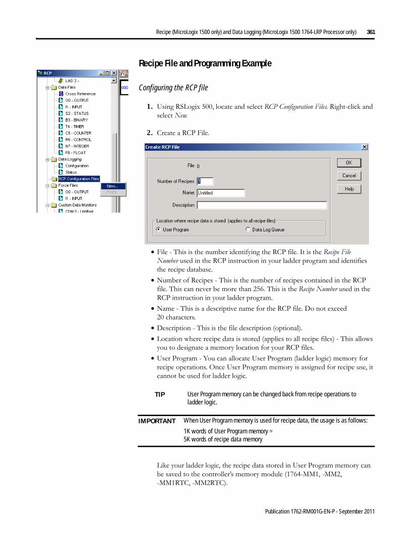
Recipe (MicroLogix 1500 only) and Data Logging (MicroLogix 1500 1764-LRP Processor only) 361
Recipe File and Programming Example
Configuring the RCP file
1. Using RSLogix 500, locate and select RCP Configuration Files. Right-click and select New.
2. Create a RCP File.
• File - This is the number identifying the RCP file. It is the Recipe File Number used in the RCP instruction in your ladder program and identifies the recipe database.
• Number of Recipes - This is the number of recipes contained in the RCP file. This can never be more than 256. This is the Recipe Number used in the RCP instruction in your ladder program.
• Name - This is a descriptive name for the RCP file. Do not exceed 20 characters.
• Description - This is the file description (optional).• Location where recipe data is stored (applies to all recipe files) - This allows
you to designate a memory location for your RCP files.• User Program - You can allocate User Program (ladder logic) memory for
recipe operations. Once User Program memory is assigned for recipe use, it cannot be used for ladder logic.
Like your ladder logic, the recipe data stored in User Program memory can be saved to the controller’s memory module (1764-MM1, -MM2, -MM1RTC, -MM2RTC).
TIP User Program memory can be changed back from recipe operations to ladder logic.
IMPORTANT When User Program memory is used for recipe data, the usage is as follows:
1K words of User Program memory = 5K words of recipe data memory
Publication 1762-RM001G-EN-P - September 2011
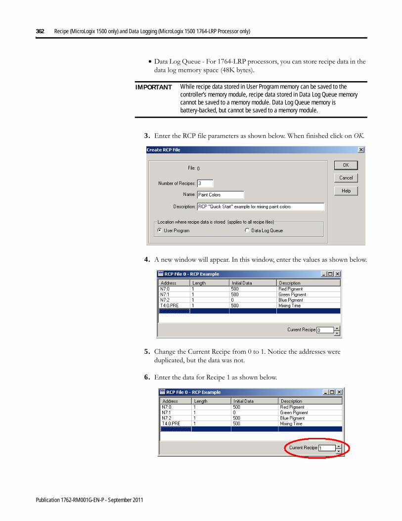
362 Recipe (MicroLogix 1500 only) and Data Logging (MicroLogix 1500 1764-LRP Processor only)
• Data Log Queue - For 1764-LRP processors, you can store recipe data in the data log memory space (48K bytes).
3. Enter the RCP file parameters as shown below. When finished click on OK.
4. A new window will appear. In this window, enter the values as shown below.
5. Change the Current Recipe from 0 to 1. Notice the addresses were duplicated, but the data was not.
6. Enter the data for Recipe 1 as shown below.
IMPORTANT While recipe data stored in User Program memory can be saved to the controller’s memory module, recipe data stored in Data Log Queue memory cannot be saved to a memory module. Data Log Queue memory is battery-backed, but cannot be saved to a memory module.
Publication 1762-RM001G-EN-P - September 2011
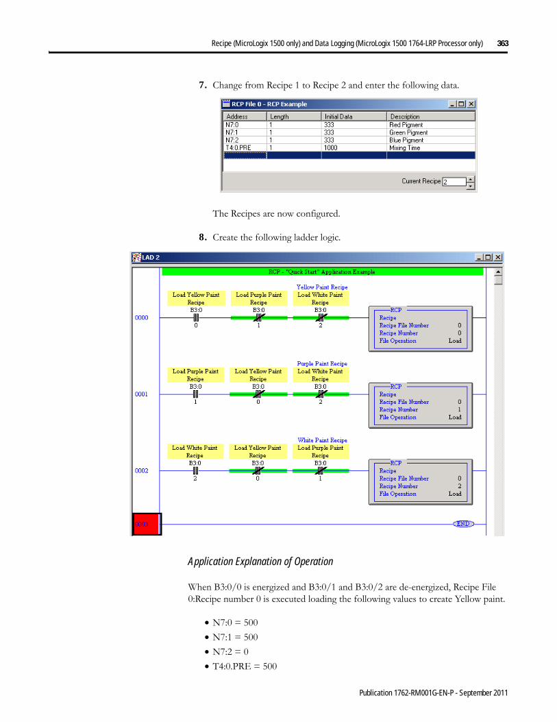
Recipe (MicroLogix 1500 only) and Data Logging (MicroLogix 1500 1764-LRP Processor only) 363
7. Change from Recipe 1 to Recipe 2 and enter the following data.
The Recipes are now configured.
8. Create the following ladder logic.
Application Explanation of Operation
When B3:0/0 is energized and B3:0/1 and B3:0/2 are de-energized, Recipe File 0:Recipe number 0 is executed loading the following values to create Yellow paint.
• N7:0 = 500• N7:1 = 500• N7:2 = 0• T4:0.PRE = 500
Publication 1762-RM001G-EN-P - September 2011

364 Recipe (MicroLogix 1500 only) and Data Logging (MicroLogix 1500 1764-LRP Processor only)
When B3:0/1 is energized and B3:0/0 and B3:0/2 are de-energized, Recipe File 0:Recipe number 1 is executed loading the following values to create Purple paint.
• N7:0 = 500• N7:1 = 0• N7:2 = 500• T4:0.PRE = 500
When B3:0/2 is energized and B3:0/0 and B3:0/1 are de-energized, Recipe File 0:Recipe number 2 is executed loading the following values to create White paint.
• N7:0 = 333• N7:1 = 333• N7:2 = 333• T4:0.PRE = 1000
Monitor the N7 data file. Notice the values change after each bit is toggled.
This example describes loading values from a RCP file to data table addresses. However, note that by changing the RCP file operation from Load to Store, values can be loaded by ladder logic into the recipe database for each Recipe number.
Data Logging Data Logging allows you to capture (store) application data as a record for retrieval at a later time. Each record is stored in a user-configured queue in battery backed memory (B-Ram). Records are retrieved from the 1764-LRP processor via communications. This chapter explains how Data Logging is configured and used.
This section contains the following topics:
• Queues and Records on page 364• Configuring Data Log Queues on page 368• DLG - Data Log Instruction on page 370• Data Log Status File on page 370• Retrieving (Reading) Records on page 372
Queues and Records The 1764-LRP processor has 48K bytes (48 x 1024) of additional memory for data logging purposes. Within this memory, you can define up to 256 (0 to 255) data logging queues. Each queue is configurable by size (maximum number of records stored), and by length (each record is 1 to 80 characters). The length and the maximum number of records determine how much memory is used by the queue. You can choose to have one large queue or multiple small queues.
Publication 1762-RM001G-EN-P - September 2011

Recipe (MicroLogix 1500 only) and Data Logging (MicroLogix 1500 1764-LRP Processor only) 365
The memory used for data logging is independent of the rest of the processor memory and cannot be accessed by the User Program. Each record is stored as the instruction is executed and is non-volatile (battery-backed) to prevent loss during power-down.
Example Queue 0
This queue is used to show how to calculate the string length of each record and maximum number of records.
String Length of Record
The size of a record is limited so that the length of the maximum formatted string does not exceed 80 characters. The following table can be used to determine the formatted string length.
Data Files Function FilesProgram Files
12
0
34 to 255
STIEII
HSCPTO
PWM
RTC
34
2
56 to 255
Q1Q2
Q0
Q3Q4 to 255
Specialty Files
Queue 0 (Date = ✔, Time = ✔, Delimiter = ,)
Date Time N7:11 L14:0 T4:5.ACC I1:3.0 B3:2Record 0 01/10/2000 , 20:00:00 , 2315 , 103457 , 200 , 8190 , 4465
Record 1 01/10/2000 , 20:30:00 , 2400 , 103456 , 250 , 8210 , 4375
Record 2 01/10/2000 , 21:00:00 , 2275 , 103455 , 225 , 8150 , 4335
Record 3 01/10/2000 , 21:30:00 , 2380 , 103455 , 223 , 8195 , 4360
Record 4 01/10/2000 , 22:00:00 , 2293 , 103456 , 218 , 8390 , 4375
Record 5 01/10/2000 , 22:30:00 , 2301 , 103455 , 231 , 8400 , 4405
Record 6 01/10/2000 , 23:00:00 , 2308 , 103456 , 215 , 8100 , 4395
Record 7 01/10/2000 , 23:30:00 , 2350 , 103457 , 208 , 8120 , 4415
Record 8 01/11/2000 , 00:00:00 , 2295 , 103457 , 209 , 8145 , 4505
Record 9 01/11/2000 , 00:30:00 , 2395 , 103456 , 211 , 8190 , 4305
Record 10 01/11/2000 , 01:00:00 , 2310 , 103455 , 224 , 8195 , 4455
Record 11 01/11/2000 , 01:30:00 , 2295 , 103456 , 233 , 8190 , 4495
Data Memory Consumed Formatted String Sizedelimiter 0 bytes 1 characterword 2 bytes 6 characterslong word 4 bytes 11 charactersdate 2 bytes 10 characterstime 2 bytes 8 characters
Publication 1762-RM001G-EN-P - September 2011

366 Recipe (MicroLogix 1500 only) and Data Logging (MicroLogix 1500 1764-LRP Processor only)
For queue 0, the formatted string length is 59 characters, as shown below:
= 10 + 1 + 8 + 1 + 6 + 1 + 11 + 1 + 6 + 1 + 6 + 1 + 6= 59 characters
Number of Records
Using Queue 0 as an example, each record consumes:
In this example, each record consumes 18 bytes. So if one queue was configured, the maximum number of records that could be stored would be 2730. The maximum number of records is calculated by:
Maximum Number of Records = Data Log File Size/Record Size= 48K bytes/18 bytes= (48)(1024)/18= 2730 records
Example Queue 5
Data Date Time N7:11 L14:0 T4:5.ACC I1:3.0 I1:2.1Characters 10 1 8 1 6 1 11 1 6 1 6 1 6
Record Field Memory ConsumptionDate 2 bytesTime 2 bytesN7:11 2 bytesL14:0 4 bytesT4:5.ACC 2 bytesI1:3.0 2 bytesB3:2 2 bytesIntegrity Check 2 bytesTotal 18 bytes
Queue 5 (Time = ✔, Delimiter = TAB)
Time N7:11 I1:3.0 I1:2.1Record 0 20:00:00 TAB 2315 TAB 8190 TAB 4465
Record 1 20:30:00 TAB 2400 TAB 8210 TAB 4375
Record 2 21:00:00 TAB 2275 TAB 8150 TAB 4335
Record 3 21:30:00 TAB 2380 TAB 8195 TAB 4360
Record 4 22:00:00 TAB 2293 TAB 8390 TAB 4375
Record 5 22:30:00 TAB 2301 TAB 8400 TAB 4405
Record 6 23:00:00 TAB 2308 TAB 8100 TAB 4395
Publication 1762-RM001G-EN-P - September 2011
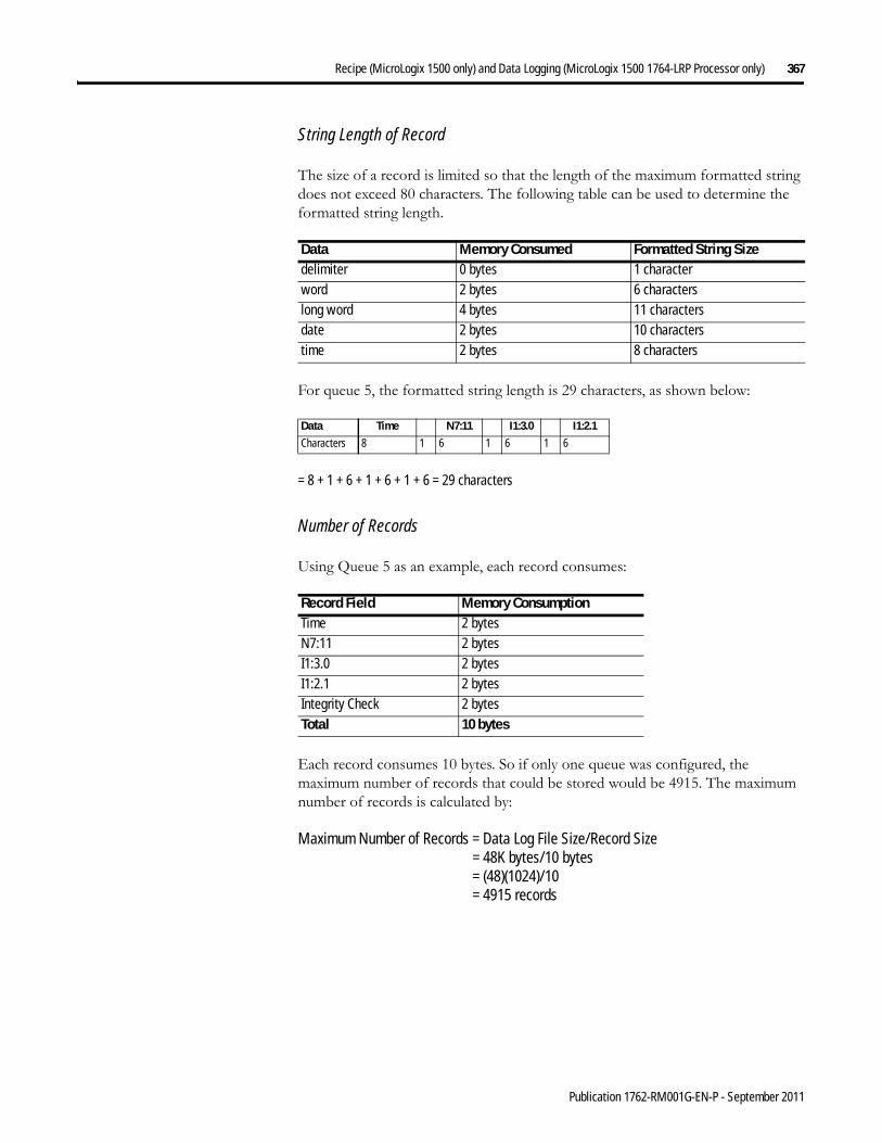
Recipe (MicroLogix 1500 only) and Data Logging (MicroLogix 1500 1764-LRP Processor only) 367
String Length of Record
The size of a record is limited so that the length of the maximum formatted string does not exceed 80 characters. The following table can be used to determine the formatted string length.
For queue 5, the formatted string length is 29 characters, as shown below:
= 8 + 1 + 6 + 1 + 6 + 1 + 6 = 29 characters
Number of Records
Using Queue 5 as an example, each record consumes:
Each record consumes 10 bytes. So if only one queue was configured, the maximum number of records that could be stored would be 4915. The maximum number of records is calculated by:
Maximum Number of Records = Data Log File Size/Record Size= 48K bytes/10 bytes= (48)(1024)/10= 4915 records
Data Memory Consumed Formatted String Sizedelimiter 0 bytes 1 characterword 2 bytes 6 characterslong word 4 bytes 11 charactersdate 2 bytes 10 characterstime 2 bytes 8 characters
Data Time N7:11 I1:3.0 I1:2.1Characters 8 1 6 1 6 1 6
Record Field Memory ConsumptionTime 2 bytesN7:11 2 bytesI1:3.0 2 bytesI1:2.1 2 bytesIntegrity Check 2 bytesTotal 10 bytes
Publication 1762-RM001G-EN-P - September 2011

368 Recipe (MicroLogix 1500 only) and Data Logging (MicroLogix 1500 1764-LRP Processor only)
Configuring Data Log Queues
Data Logging is configured using RSLogix 500 programming software version V4.00.00 or later.
1. Open a 1764-LRP application. The first step in using Data Logging is to configure the data log queue(s). Access to this function is provided via the RSLogix 500 Project tree:
2. The Data Log Que window appears. Double-click on Data Log Configuration.
Double-click Configuration to access Data Log Configuration.
Appearance of Data Log Que Configuration window before creating a queue.
Publication 1762-RM001G-EN-P - September 2011

Recipe (MicroLogix 1500 only) and Data Logging (MicroLogix 1500 1764-LRP Processor only) 369
3. The Data Log Que dialog box appears as shown below. Use this dialog box to enter the queue information.
Enter the following information:
4. After entering all the information for the data log queue, click on OK. The queue is added to the Data Log Que window with a corresponding queue number. This is the queue number to use in the DLG instruction.
Data Log Queue Configuration Parameter
Description
Number of Records Defines the number of records (data sets) in the queue.
Separator Character Choose the character to act as the separator for the data in this queue (tab, comma, or space). The separator character may be the same or different for each queue configured.
Date Stamp (optional) if selected, the date is recorded in mm/dd/yyyy format(1).
(1) If the real-time clock is not present on the controller and Date Stamp and Time Stamp are selected (enabled), the date is recorded as 00/00/0000 and the time as 00:00:00.
Time Stamp (optional) if selected, the time is recorded in hh:mm:ss format(1).
Address to Log Enter the address of an item to be recorded and click on Accept to add the address to the Current Address List. The address can be any 16 or 32-bit piece of data.
Current Address List This is the list of items to be recorded. Record size can be up to 80 bytes. You can use the Delete button to remove items from this list. See page 365 for information on record size.
A record consists of configured Date Stamp, Time Stamp, Current Address List, and Separator Characters.
Publication 1762-RM001G-EN-P - September 2011

370 Recipe (MicroLogix 1500 only) and Data Logging (MicroLogix 1500 1764-LRP Processor only)
DLG - Data Log Instruction
Instruction Type: output
The DLG instruction triggers the saving of a record. The DLG instruction has one operand:
Queue Number - Specifies which data log queue captures a record.
The DLG instruction only captures data on a false-to-true rung transition. The DLG rung must be reset (scanned false) before it will capture data again. Never place the DLG instruction alone on a rung. It should always have preceding logic, as shown below:
Data Log Status File There is a Data Log Status (DLS) file element for each Data Log Queue. The DLS file does not exist until a data log queue has been configured.
The Data Log Status file has 3-word elements. Word 0 is addressable by bit only through ladder logic. Words 1 and 2 are addressable by word and/or bit through ladder logic.
The number of DLS file elements depends upon the number of queues specified in the application. The status bits and words are described below.
DLGData Logqueue number 0
DLGExecution Time for the DLG Instruction
Controller When Rung Is:True False
MicroLogix 1500 1764-LRP 67.5 μs + 11.8 μs/date stamp
+ 12.4 μs/time stamp
+ 9.1 μs/word logged
+ 16.2 μs/long word logged
6.7 μs
IMPORTANT You must configure a data log queue before programming a DLG instruction into your ladder program.
Data Logqueue number 0
DLG
Data Log Status (DLS) File Elements
Control ElementWord 15 14 13 12 11 10 09 08 07 06 05 04 03 02 01 000 EN(1) 0 DN(2) OV(3) 0 0 0 0 0 0 0 0 0 0 0 0
Publication 1762-RM001G-EN-P - September 2011

Recipe (MicroLogix 1500 only) and Data Logging (MicroLogix 1500 1764-LRP Processor only) 371
Data Logging Enable (EN)
When the DLG instruction rung is true, the Data Logging Enable (EN) is set (1) and the DLG instruction records the defined data set. To address this bit in ladder logic, use the format: DLS0:Q/EN, where Q is the queue number.
Data Logging Done (DN)
The Data Logging Done (DN) bit is used to indicate when the associated queue is full. This bit is set (1) by the DLG instruction when the queue becomes full. This bit is cleared when a record is retrieved from the queue. To address this bit in ladder logic, use the format: DLS0:Q/DN, were Q is the queue number.
Data Logging Overflow (OV)
The Data Logging Overflow (OV) bit is used to indicate when a record gets overwritten in the associated queue. This bit is set (1) by the DLG instruction when a record is overwritten. Once set, the OV bit remains set until you clear (0) it. To address this bit in ladder logic, use the format: DLS0:Q/OV, where Q is the queue number.
File Size (FSZ)
File Size (FSZ) shows the number of records that are allocated for this queue. The number of records is set when the data log queue is configured. FSZ can be used with RST to determine how full the queue is. To address this word in ladder logic, use the format: DLS0:Q.FSZ, where Q is the queue number.
Records Stored (RST)
Records Stored (RST) specifies how many data sets are in the queue. RST is decremented when a record is read from a communications device. To address this word in ladder logic, use the format: DLS0:Q.RST, where Q is the queue number.
1 FSZ = File Size (number of records allocated)
2 RST = Records Stored (number of records recorded)
(1) EN = Enable Bit
(2) DN = Done Bit
(3) OV = Overflow Bit
Data Log Status (DLS) File Elements
Control ElementWord 15 14 13 12 11 10 09 08 07 06 05 04 03 02 01 00
Publication 1762-RM001G-EN-P - September 2011
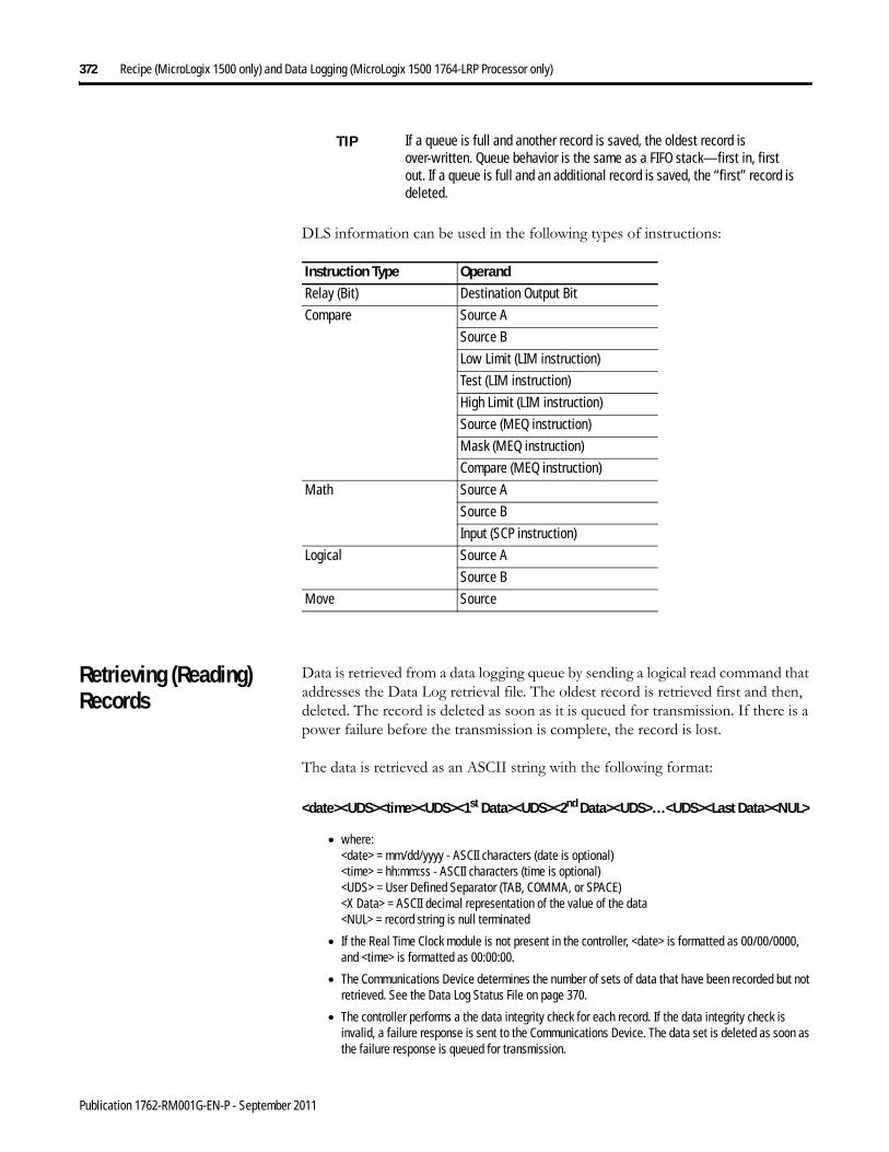
372 Recipe (MicroLogix 1500 only) and Data Logging (MicroLogix 1500 1764-LRP Processor only)
DLS information can be used in the following types of instructions:
Retrieving (Reading) Records
Data is retrieved from a data logging queue by sending a logical read command that addresses the Data Log retrieval file. The oldest record is retrieved first and then, deleted. The record is deleted as soon as it is queued for transmission. If there is a power failure before the transmission is complete, the record is lost.
The data is retrieved as an ASCII string with the following format:
<date><UDS><time><UDS><1st Data><UDS><2nd Data><UDS>…<UDS><Last Data><NUL>
• where:<date> = mm/dd/yyyy - ASCII characters (date is optional)<time> = hh:mm:ss - ASCII characters (time is optional)<UDS> = User Defined Separator (TAB, COMMA, or SPACE)<X Data> = ASCII decimal representation of the value of the data<NUL> = record string is null terminated
• If the Real Time Clock module is not present in the controller, <date> is formatted as 00/00/0000, and <time> is formatted as 00:00:00.
• The Communications Device determines the number of sets of data that have been recorded but not retrieved. See the Data Log Status File on page 370.
• The controller performs a the data integrity check for each record. If the data integrity check is invalid, a failure response is sent to the Communications Device. The data set is deleted as soon as the failure response is queued for transmission.
TIP If a queue is full and another record is saved, the oldest record is over-written. Queue behavior is the same as a FIFO stack—first in, first out. If a queue is full and an additional record is saved, the “first” record is deleted.
Instruction Type OperandRelay (Bit) Destination Output Bit
Compare Source A
Source B
Low Limit (LIM instruction)
Test (LIM instruction)
High Limit (LIM instruction)
Source (MEQ instruction)
Mask (MEQ instruction)
Compare (MEQ instruction)
Math Source A
Source B
Input (SCP instruction)
Logical Source A
Source B
Move Source
Publication 1762-RM001G-EN-P - September 2011
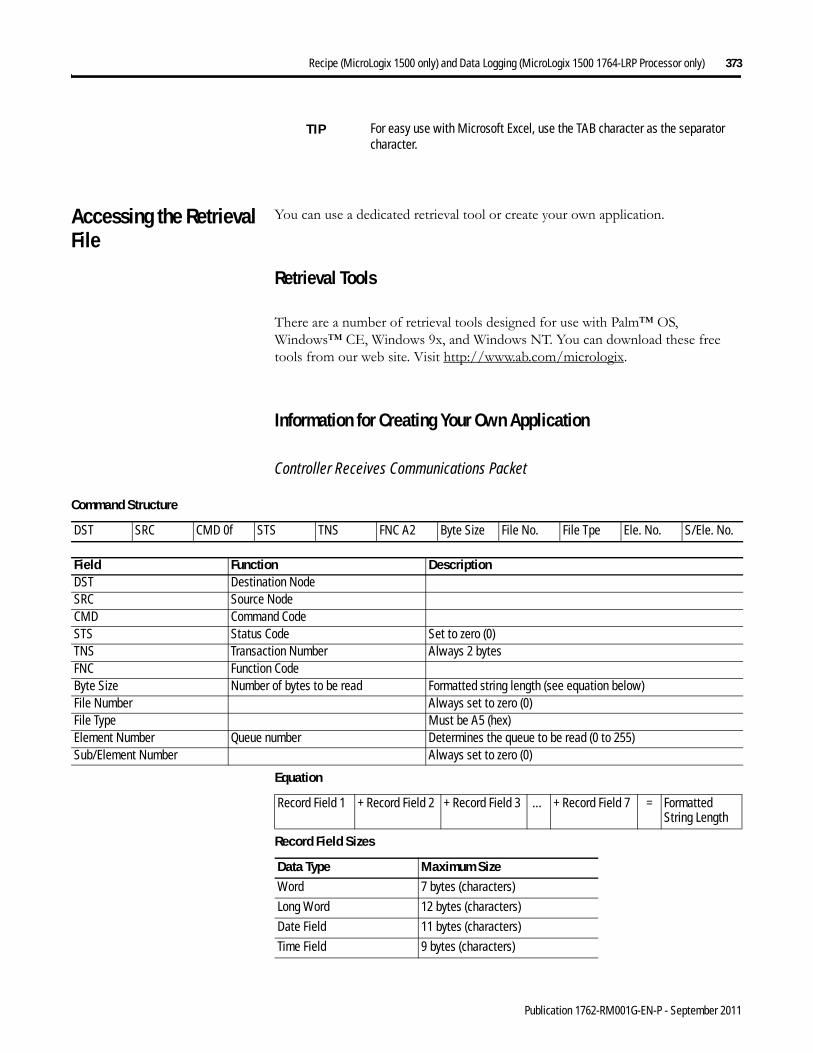
Recipe (MicroLogix 1500 only) and Data Logging (MicroLogix 1500 1764-LRP Processor only) 373
Accessing the Retrieval File
You can use a dedicated retrieval tool or create your own application.
Retrieval Tools
There are a number of retrieval tools designed for use with Palm™ OS, Windows™ CE, Windows 9x, and Windows NT. You can download these free tools from our web site. Visit http://www.ab.com/micrologix.
Information for Creating Your Own Application
Controller Receives Communications Packet
TIP For easy use with Microsoft Excel, use the TAB character as the separator character.
Command Structure
DST SRC CMD 0f STS TNS FNC A2 Byte Size File No. File Tpe Ele. No. S/Ele. No.
Field Function DescriptionDST Destination NodeSRC Source NodeCMD Command CodeSTS Status Code Set to zero (0)TNS Transaction Number Always 2 bytesFNC Function CodeByte Size Number of bytes to be read Formatted string length (see equation below)File Number Always set to zero (0)File Type Must be A5 (hex)Element Number Queue number Determines the queue to be read (0 to 255)Sub/Element Number Always set to zero (0)
Equation
Record Field 1 + Record Field 2 + Record Field 3 … + Record Field 7 = Formatted String Length
Record Field Sizes
Data Type Maximum SizeWord 7 bytes (characters)
Long Word 12 bytes (characters)
Date Field 11 bytes (characters)
Time Field 9 bytes (characters)
Publication 1762-RM001G-EN-P - September 2011

374 Recipe (MicroLogix 1500 only) and Data Logging (MicroLogix 1500 1764-LRP Processor only)
Controller Responds with Reply
If the data integrity check fails, the record is deleted and an error is sent with STS of 0xF0 and ext STS of 0x0E.
For more information on writing a DF1 protocol, refer to Allen-Bradley publication 1770-6.5.16, DF1 Protocol and Command Set Reference Manual (available from www.theautomationbookstore.com).
Conditions that Will Erase the Data Retrieval File
The following conditions will cause previously logged data to be lost:
• Program download from RSLogix 500 to controller.• Memory Module transfer to controller except for Memory Module autoload of the
same program.• Full Queue - when a queue is full, new records are recorded over the existing
records, starting at the beginning of the file. You can put the following rung in your ladder program to prevent this from happening:
TIP The formatted string length cannot exceed 80 bytes in length.
TIP The last byte will be a zero value representing the terminator character.
Reply Structure
SRC DST CMD 4f STS TNS DATA EXT STS
Field Function DescriptionSRC Source Node DST Destination NodeCMD Command CodeSTS Status CodeTNS Transaction Number Always 2 bytesDATA Formatted string
IMPORTANT The data in the retrieval file can only be read once. Then it is erased from the processor.
B3:1
1
LEQLess Than or Eql (A<=B)Source A DLS0:5.RST Source B DLS0:5.FSZ
LEQ DLGData Logqueue number 5
DLG
Publication 1762-RM001G-EN-P - September 2011
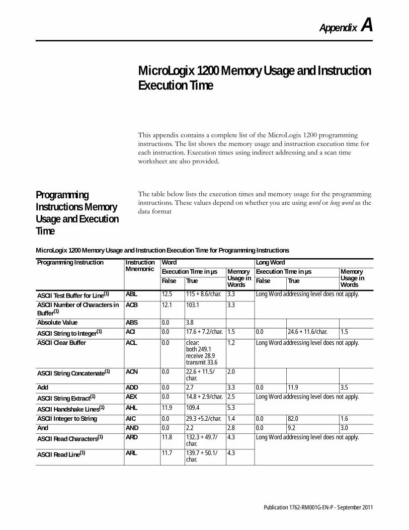
Appendix A
MicroLogix 1200 Memory Usage and Instruction Execution Time
This appendix contains a complete list of the MicroLogix 1200 programming instructions. The list shows the memory usage and instruction execution time for each instruction. Execution times using indirect addressing and a scan time worksheet are also provided.
Programming Instructions Memory Usage and Execution Time
The table below lists the execution times and memory usage for the programming instructions. These values depend on whether you are using word or long word as the data format
MicroLogix 1200 Memory Usage and Instruction Execution Time for Programming Instructions
Programming Instruction Instruction Mnemonic
Word Long WordExecution Time in µs Memory
Usage in Words
Execution Time in µs Memory Usage in WordsFalse True False True
ASCII Test Buffer for Line(1) ABL 12.5 115 + 8.6/char. 3.3 Long Word addressing level does not apply.
ASCII Number of Characters in Buffer(1)
ACB 12.1 103.1 3.3
Absolute Value ABS 0.0 3.8
ASCII String to Integer(1) ACI 0.0 17.6 + 7.2/char. 1.5 0.0 24.6 + 11.6/char. 1.5
ASCII Clear Buffer ACL 0.0 clear:both 249.1receive 28.9transmit 33.6
1.2 Long Word addressing level does not apply.
ASCII String Concatenate(1) ACN 0.0 22.6 + 11.5/char.
2.0
Add ADD 0.0 2.7 3.3 0.0 11.9 3.5
ASCII String Extract(1) AEX 0.0 14.8 + 2.9/char. 2.5 Long Word addressing level does not apply.
ASCII Handshake Lines(1) AHL 11.9 109.4 5.3
ASCII Integer to String AIC 0.0 29.3 +5.2/char. 1.4 0.0 82.0 1.6And AND 0.0 2.2 2.8 0.0 9.2 3.0
ASCII Read Characters(1) ARD 11.8 132.3 + 49.7/char.
4.3 Long Word addressing level does not apply.
ASCII Read Line(1) ARL 11.7 139.7 + 50.1/char.
4.3
375 Publication 1762-RM001G-EN-P - September 2011

376 MicroLogix 1200 Memory Usage and Instruction Execution Time
ASCII String Search(1) ASC 0.0 16.2 + 4.0/matching char.
6.0 Long Word addressing level does not apply.
ASCII String Compare(1) ASR 0.0 9.2 + 4.0/matching char.
1.8
ASCII Write with Append AWA 14.1 268 + 12/char. 3.4ASCII Write AWT 14.1 268 + 12/char. 3.4Bit Shift Left BSL 1.3 32 + 1.3/word 3.8Bit Shift Right BSR 1.3 32 + 1.3/word 3.8Clear CLR 0.0 1.3 1.0 0.0 6.3 1.0File Copy COP 0.0 19 + 0.8/word 2.0 Long Word addressing level does not apply.Copy Word CPW 0.0 18.3 + 0.8/wordCount Down CTD 9.0 9.0 2.4Count Up CTU 9.2 9.0 2.4Decode 4-to-1 of 16 DCD 0.0 1.9 1.9Divide DIV 0.0 12.2 2.0 0.0 42.8 3.5Encode 1-of-16 to 4 ENC 0.0 7.2 1.5 Long Word addressing level does not apply.Equal EQU 1.1 1.3 1.3 1.9 2.8 2.6FIFO Load FFL 11.1 11.3 3.4 11.2 11.7 3.9FIFO Unload FFU 10.4 33 + 0.8/word 3.4 10.4 36 + 1.5/long word 3.4Fill File FLL 0.0 14 + 0.6/word 2.0 0.0 15 + 1.2/long word 2.5Convert from BCD FRD 0.0 14.1 1.5 Long Word addressing level does not apply.Gray Code GCD 0.0 9.5Greater Than or Equal To GEQ 1.1 1.3 1.3 2.7 2.8 2.9Greater Than GRT 1.1 1.3 1.3 2.7 2.8 2.4High-Speed Load HSL 0.0 46.7 7.3 0.0 47.3 7.8Immediate Input with Mask IIM 0.0 26.4 3.0 Long Word addressing level does not apply.Interrupt Subroutine INT 1.0 1.0 0.3Immediate Output with Mask IOM 0.0 22.3 3.0Jump JMP 0.0 1.0 0.5Jump to Subroutine JSR 0.0 8.4 1.5Label LBL 1.0 1.0 0.5Less Than or Equal To LEQ 1.1 1.3 1.3 2.7 2.8 2.9Less Than LES 1.1 1.3 1.3 2.7 2.8 2.9LIFO Load LFL 10.4 25.5 3.4 10.4 31.6 3.9LIFO Unload LFU 10.4 29.1 3.4 10.4 31.6 3.4Limit LIM 6.1 6.4 2.3 13.6 14.4 4.0Master Control Reset MCR (Start) 1.2 1.2 1.0 Long Word addressing level does not apply.
MCR (End) 1.6 1.6 1.5Masked Comparison for Equal MEQ 1.8 1.9 1.8 3.1 3.9 3.5Move MOV 0.0 2.4 2.5 0.0 8.3 2.0
MicroLogix 1200 Memory Usage and Instruction Execution Time for Programming Instructions
Programming Instruction Instruction Mnemonic
Word Long WordExecution Time in µs Memory
Usage in Words
Execution Time in µs Memory Usage in WordsFalse True False True
Publication 1762-RM001G-EN-P - September 2011
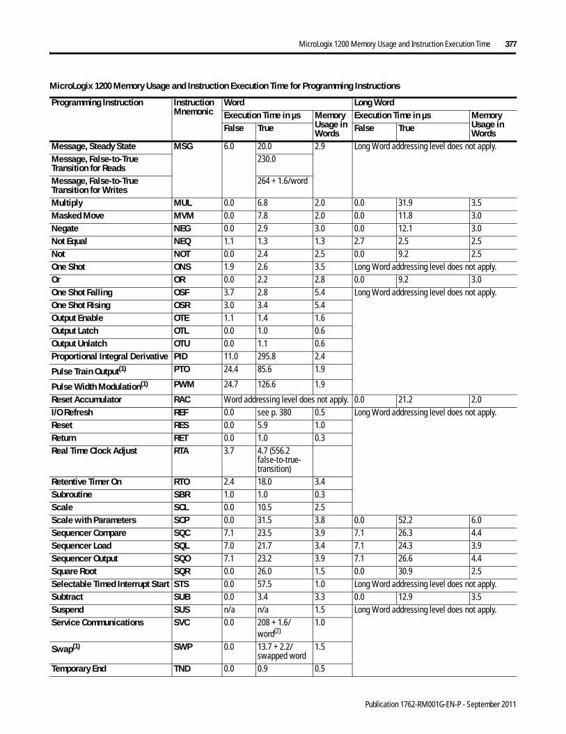
MicroLogix 1200 Memory Usage and Instruction Execution Time 377
Message, Steady State MSG 6.0 20.0 2.9 Long Word addressing level does not apply.Message, False-to-True Transition for Reads
230.0
Message, False-to-True Transition for Writes
264 + 1.6/word
Multiply MUL 0.0 6.8 2.0 0.0 31.9 3.5Masked Move MVM 0.0 7.8 2.0 0.0 11.8 3.0Negate NEG 0.0 2.9 3.0 0.0 12.1 3.0Not Equal NEQ 1.1 1.3 1.3 2.7 2.5 2.5Not NOT 0.0 2.4 2.5 0.0 9.2 2.5One Shot ONS 1.9 2.6 3.5 Long Word addressing level does not apply.Or OR 0.0 2.2 2.8 0.0 9.2 3.0One Shot Falling OSF 3.7 2.8 5.4 Long Word addressing level does not apply.One Shot Rising OSR 3.0 3.4 5.4Output Enable OTE 1.1 1.4 1.6Output Latch OTL 0.0 1.0 0.6Output Unlatch OTU 0.0 1.1 0.6Proportional Integral Derivative PID 11.0 295.8 2.4
Pulse Train Output(1) PTO 24.4 85.6 1.9
Pulse Width Modulation(1) PWM 24.7 126.6 1.9
Reset Accumulator RAC Word addressing level does not apply. 0.0 21.2 2.0I/O Refresh REF 0.0 see p. 380 0.5 Long Word addressing level does not apply.Reset RES 0.0 5.9 1.0Return RET 0.0 1.0 0.3Real Time Clock Adjust RTA 3.7 4.7 (556.2
false-to-true-transition)
Retentive Timer On RTO 2.4 18.0 3.4Subroutine SBR 1.0 1.0 0.3Scale SCL 0.0 10.5 2.5Scale with Parameters SCP 0.0 31.5 3.8 0.0 52.2 6.0Sequencer Compare SQC 7.1 23.5 3.9 7.1 26.3 4.4Sequencer Load SQL 7.0 21.7 3.4 7.1 24.3 3.9Sequencer Output SQO 7.1 23.2 3.9 7.1 26.6 4.4Square Root SQR 0.0 26.0 1.5 0.0 30.9 2.5Selectable Timed Interrupt Start STS 0.0 57.5 1.0 Long Word addressing level does not apply.Subtract SUB 0.0 3.4 3.3 0.0 12.9 3.5Suspend SUS n/a n/a 1.5 Long Word addressing level does not apply.Service Communications SVC 0.0 208 + 1.6/
word(2)1.0
Swap(1) SWP 0.0 13.7 + 2.2/swapped word
1.5
Temporary End TND 0.0 0.9 0.5
MicroLogix 1200 Memory Usage and Instruction Execution Time for Programming Instructions
Programming Instruction Instruction Mnemonic
Word Long WordExecution Time in µs Memory
Usage in Words
Execution Time in µs Memory Usage in WordsFalse True False True
Publication 1762-RM001G-EN-P - September 2011

378 MicroLogix 1200 Memory Usage and Instruction Execution Time
Indirect Addressing
The following sections describe how indirect addressing affects the execution time of instructions for the Micrologix 1200 controllers. The timing for an indirect address is affected by the form of the indirect address.
For the address forms in the following table, you can interchange the following file types:
• Input (I) and Output (O)• Bit (B), Integer (N)• Timer (T), Counter (C), and Control (R)
Execution Times for the Indirect Addresses
For most types of instructions that contain an indirect address(es), look up the form of the indirect address in the table below and add that time to the execution time of the instruction.
[*] indicates that an indirect reference is substituted.
Convert to BCD TOD 0.0 17.2 1.8 Long Word addressing level does not apply.Off-Delay Timer TOF 13.0 2.9 3.9On-Delay Timer TON 3.0 18.0 3.9User Interrupt Disable UID 0.0 0.8 0.9User Interrupt Enable UIE 0.0 0.8 0.9User Interrupt Flush UIF 0.0 12.3 0.9Examine if Closed XIC 0.8 0.9 1.0Examine if Open XIO 0.8 0.9 1.0Exclusive Or XOR 0.0 3.0 2.8 0.0 9.9 3.0
(1) Only valid for MicroLogix 1200 Series B Controllers.
(2) This value for the SVC instruction is for when the communications servicing function is accessing a data file. The time increases when accessing a function file.
MicroLogix 1200 Memory Usage and Instruction Execution Time for Programming Instructions
Programming Instruction Instruction Mnemonic
Word Long WordExecution Time in µs Memory
Usage in Words
Execution Time in µs Memory Usage in WordsFalse True False True
MicroLogix 1200 Instruction Execution Time Using Indirect Addressing
Address Form Operand Time (µs) Address Form Operand Time (µs)O:1.[*] 5.8 B3:1/[*] 6.8O:[*].0 15.0 B3:[*]/[*] 7.6O:[*].[*] 15.1 B[*]:1/[*] 25.9B3:[*] 5.8 B[*]:[*]/[*] 26.2
Publication 1762-RM001G-EN-P - September 2011
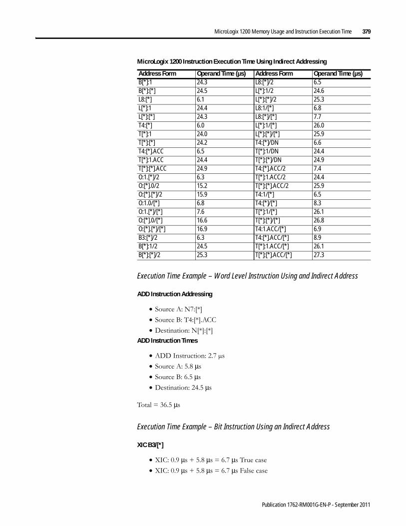
MicroLogix 1200 Memory Usage and Instruction Execution Time 379
Execution Time Example – Word Level Instruction Using and Indirect Address
ADD Instruction Addressing
• Source A: N7:[*]• Source B: T4:[*].ACC• Destination: N[*]:[*]
ADD Instruction Times
• ADD Instruction: 2.7 µs• Source A: 5.8 μs• Source B: 6.5 μs• Destination: 24.5 μs
Total = 36.5 μs
Execution Time Example – Bit Instruction Using an Indirect Address
XIC B3/[*]
• XIC: 0.9 μs + 5.8 μs = 6.7 μs True case• XIC: 0.9 μs + 5.8 μs = 6.7 μs False case
B[*]:1 24.3 L8:[*]/2 6.5B[*]:[*] 24.5 L[*]:1/2 24.6L8:[*] 6.1 L[*]:[*]/2 25.3L[*]:1 24.4 L8:1/[*] 6.8L[*]:[*] 24.3 L8:[*]/[*] 7.7T4:[*] 6.0 L[*]:1/[*] 26.0T[*]:1 24.0 L[*]:[*]/[*] 25.9T[*]:[*] 24.2 T4:[*]/DN 6.6T4:[*].ACC 6.5 T[*]:1/DN 24.4T[*]:1.ACC 24.4 T[*]:[*]/DN 24.9T[*]:[*].ACC 24.9 T4:[*].ACC/2 7.4O:1.[*]/2 6.3 T[*]:1.ACC/2 24.4O:[*].0/2 15.2 T[*]:[*].ACC/2 25.9O:[*].[*]/2 15.9 T4:1/[*] 6.5O:1.0/[*] 6.8 T4:[*]/[*] 8.3O:1.[*]/[*] 7.6 T[*]:1/[*] 26.1O:[*].0/[*] 16.6 T[*]:[*]/[*] 26.8O:[*].[*]/[*] 16.9 T4:1.ACC/[*] 6.9B3:[*]/2 6.3 T4:[*].ACC/[*] 8.9B[*]:1/2 24.5 T[*]:1.ACC/[*] 26.1B[*]:[*]/2 25.3 T[*]:[*].ACC/[*] 27.3
MicroLogix 1200 Instruction Execution Time Using Indirect Addressing
Address Form Operand Time (µs) Address Form Operand Time (µs)
Publication 1762-RM001G-EN-P - September 2011

380 MicroLogix 1200 Memory Usage and Instruction Execution Time
MicroLogix 1200 Scan Time Worksheet
Calculate the scan time for your control program using the worksheet below.
Communications Multiplier Table
Input Scan (sum of below)Overhead (if expansion I/O is used) = 55 µsExpansion Input Words X 10 µs (or X 14 µs if Forcing is used) =Number of modules with Input words X 80 µs =
Input Scan Sub-Total =Program ScanAdd execution times of all instructions in your program when executed true =Program Scan Sub-Total =Output Scan (sum of below)Overhead (if expansion I/O used) = 30 µs
Expansion Output Words X 3 µs (or X 7 µs if Forcing is used) =Output Scan Sub-Total =
Communications Overhead(1)
Worst Case =1470 µsTypical Case = 530 µsUse this number if the communications port is configured, but not communicating to any other device.
= 200 µs
Use this number if the communications port is in “Shutdown” mode. = 0 µsCommunications Overhead Sub-Total =
System OverheadAdd this number if your system includes a 1762-RTC or 1762-MM1RTC. = 100 µsHousekeeping Overhead = 270 µs
System Overhead Sub-Total =Totals
Sum of all sub-totalsMultiply by Communications Multiplier from Table X
Total Estimated Scan Time =
(1) Communications Overhead is a function of the device connected to the controller. This will not occur every scan.
ProtocolMultiplier at Various Baud Rates38.4K 19.2K 9.6K 4.8K 2.4K 1.2K 600 300 Inactive(1)
DF1 Full-Duplex 1.50 1.27 1.16 1.12 1.10 1.09 1.09 1.08 1.00DF1 Half Duplex 1.21 1.14 1.10 1.09 1.08 1.08 1.08 1.07 1.01DH-485 N/A 1.16 1.11 N/A N/A N/A N/A N/A 1.10 at 19.2K
1.07 at 9.6KModbus™ 1.22 1.13 1.10 1.09 1.09 1.09 1.09 1.09 1.00ASCII 1.55 1.33 1.26 1.22 1.21 1.19 1.19 1.18 1.01Shut Down 1.00 1.00 1.00 1.00 1.00 1.00 1.00 1.00 1.00
(1) Inactive is defined as No Messaging and No Data Monitoring. For DH-485 protocol, inactive means that the controller is not connected to a network.
Publication 1762-RM001G-EN-P - September 2011
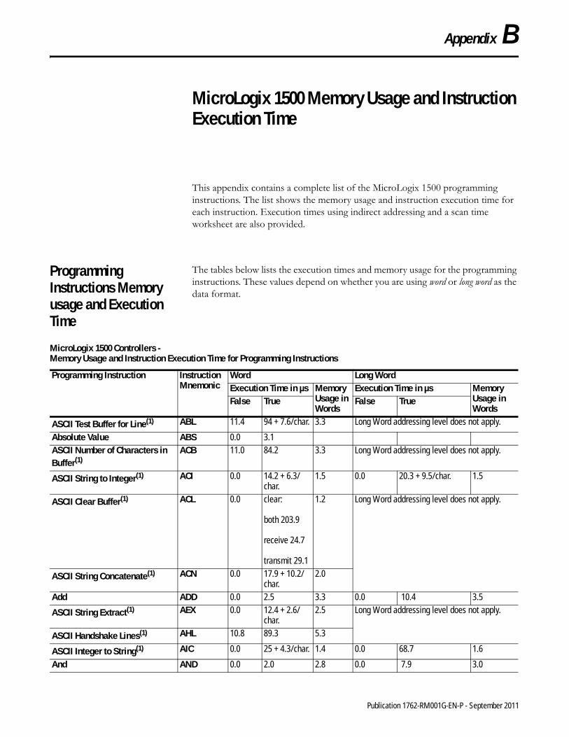
Appendix B
MicroLogix 1500 Memory Usage and Instruction Execution Time
This appendix contains a complete list of the MicroLogix 1500 programming instructions. The list shows the memory usage and instruction execution time for each instruction. Execution times using indirect addressing and a scan time worksheet are also provided.
Programming Instructions Memory usage and Execution Time
The tables below lists the execution times and memory usage for the programming instructions. These values depend on whether you are using word or long word as the data format.
MicroLogix 1500 Controllers - Memory Usage and Instruction Execution Time for Programming Instructions
Programming Instruction Instruction Mnemonic
Word Long WordExecution Time in µs Memory
Usage in Words
Execution Time in µs Memory Usage in Words
False True False True
ASCII Test Buffer for Line(1) ABL 11.4 94 + 7.6/char. 3.3 Long Word addressing level does not apply.
Absolute Value ABS 0.0 3.1ASCII Number of Characters in Buffer(1)
ACB 11.0 84.2 3.3 Long Word addressing level does not apply.
ASCII String to Integer(1) ACI 0.0 14.2 + 6.3/char.
1.5 0.0 20.3 + 9.5/char. 1.5
ASCII Clear Buffer(1) ACL 0.0 clear:
both 203.9
receive 24.7
transmit 29.1
1.2 Long Word addressing level does not apply.
ASCII String Concatenate(1) ACN 0.0 17.9 + 10.2/char.
2.0
Add ADD 0.0 2.5 3.3 0.0 10.4 3.5
ASCII String Extract(1) AEX 0.0 12.4 + 2.6/char.
2.5 Long Word addressing level does not apply.
ASCII Handshake Lines(1) AHL 10.8 89.3 5.3
ASCII Integer to String(1) AIC 0.0 25 + 4.3/char. 1.4 0.0 68.7 1.6
And AND 0.0 2.0 2.8 0.0 7.9 3.0
381 Publication 1762-RM001G-EN-P - September 2011
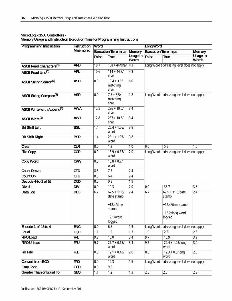
382 MicroLogix 1500 Memory Usage and Instruction Execution Time
ASCII Read Characters(1) ARD 10.7 108 + 44/char. 4.3 Long Word addressing level does not apply.
ASCII Read Line(1) ARL 10.6 114 + 44.3/char.
4.3
ASCII String Search(1) ASC 0.0 13.4 + 3.5/matching char.
6.0
ASCII String Compare(1) ASR 0.0 7.5 + 3.5/matching char.
1.8 Long Word addressing level does not apply.
ASCII Write with Append(1) AWA 12.5 236 + 10.6/char.
3.4
ASCII Write(1) AWT 12.8 237 + 10.6/char.
3.4
Bit Shift Left BSL 1.4 26.4 + 1.06/word
3.8
Bit Shift Right BSR 1.4 26.1 + 1.07/word
3.8
Clear CLR 0.0 1.2 1.0 0.0 5.5 1.0File Copy COP 0.0 15.9 + 0.67/
word2.0 Long Word addressing level does not apply.
Copy Word CPW 0.0 15.8 + 0.7/word
Count Down CTD 8.5 7.5 2.4Count Up CTU 8.5 6.4 2.4Decode 4-to-1 of 16 DCD 0.0 0.9 1.9Divide DIV 0.0 10.3 2.0 0.0 36.7 3.5Data Log DLG 6.7 67.5 + 11.8/
date stamp
+12.4/time stamp
+9.1/word logged
2.4 6.7 67.5 + 11.8/date stamp
+12.4/time stamp
+16.2/long word logged
2.4
Encode 1-of-16 to 4 ENC 0.0 6.8 1.5 Long Word addressing level does not apply.Equal EQU 1.1 1.2 1.3 1.9 2.6 2.6FIFO Load FFL 9.8 10.0 3.4 9.7 10.9 3.9FIFO Unload FFU 9.7 27.7 + 0.65/
word3.4 9.7 29.4 + 1.25/long
word 3.4
Fill File FLL 0.0 12.1 + 0.43/word
2.0 0.0 12.3 + 0.8/long word
2.5
Convert from BCD FRD 0.0 12.3 1.5 Long Word addressing level does not apply.Gray Code GCD 0.0 9.5Greater Than or Equal To GEQ 1.1 1.2 1.3 2.5 2.6 2.9
MicroLogix 1500 Controllers - Memory Usage and Instruction Execution Time for Programming Instructions
Programming Instruction Instruction Mnemonic
Word Long WordExecution Time in µs Memory
Usage in Words
Execution Time in µs Memory Usage in Words
False True False True
Publication 1762-RM001G-EN-P - September 2011
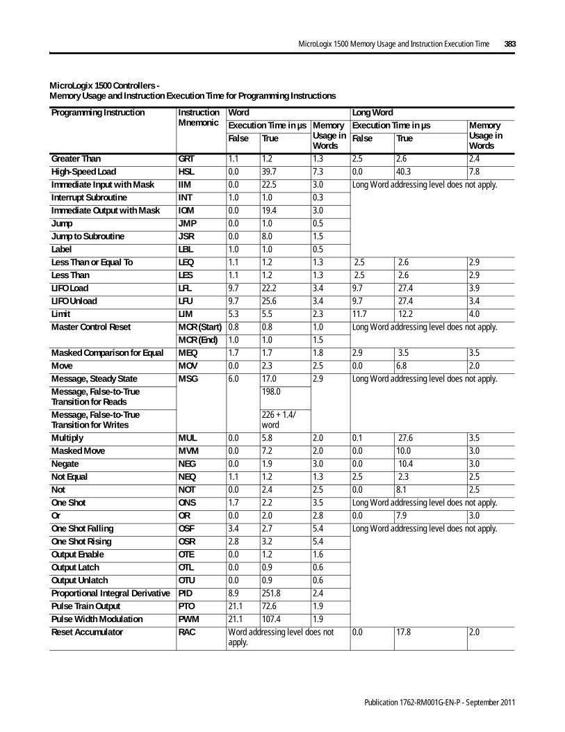
MicroLogix 1500 Memory Usage and Instruction Execution Time 383
Greater Than GRT 1.1 1.2 1.3 2.5 2.6 2.4High-Speed Load HSL 0.0 39.7 7.3 0.0 40.3 7.8Immediate Input with Mask IIM 0.0 22.5 3.0 Long Word addressing level does not apply.Interrupt Subroutine INT 1.0 1.0 0.3Immediate Output with Mask IOM 0.0 19.4 3.0Jump JMP 0.0 1.0 0.5Jump to Subroutine JSR 0.0 8.0 1.5Label LBL 1.0 1.0 0.5Less Than or Equal To LEQ 1.1 1.2 1.3 2.5 2.6 2.9Less Than LES 1.1 1.2 1.3 2.5 2.6 2.9LIFO Load LFL 9.7 22.2 3.4 9.7 27.4 3.9LIFO Unload LFU 9.7 25.6 3.4 9.7 27.4 3.4Limit LIM 5.3 5.5 2.3 11.7 12.2 4.0Master Control Reset MCR (Start) 0.8 0.8 1.0 Long Word addressing level does not apply.
MCR (End) 1.0 1.0 1.5Masked Comparison for Equal MEQ 1.7 1.7 1.8 2.9 3.5 3.5Move MOV 0.0 2.3 2.5 0.0 6.8 2.0Message, Steady State MSG 6.0 17.0 2.9 Long Word addressing level does not apply.Message, False-to-True Transition for Reads
198.0
Message, False-to-True Transition for Writes
226 + 1.4/word
Multiply MUL 0.0 5.8 2.0 0.1 27.6 3.5Masked Move MVM 0.0 7.2 2.0 0.0 10.0 3.0Negate NEG 0.0 1.9 3.0 0.0 10.4 3.0Not Equal NEQ 1.1 1.2 1.3 2.5 2.3 2.5Not NOT 0.0 2.4 2.5 0.0 8.1 2.5One Shot ONS 1.7 2.2 3.5 Long Word addressing level does not apply.Or OR 0.0 2.0 2.8 0.0 7.9 3.0One Shot Falling OSF 3.4 2.7 5.4 Long Word addressing level does not apply.One Shot Rising OSR 2.8 3.2 5.4Output Enable OTE 0.0 1.2 1.6Output Latch OTL 0.0 0.9 0.6Output Unlatch OTU 0.0 0.9 0.6Proportional Integral Derivative PID 8.9 251.8 2.4Pulse Train Output PTO 21.1 72.6 1.9Pulse Width Modulation PWM 21.1 107.4 1.9Reset Accumulator RAC Word addressing level does not
apply.0.0 17.8 2.0
MicroLogix 1500 Controllers - Memory Usage and Instruction Execution Time for Programming Instructions
Programming Instruction Instruction Mnemonic
Word Long WordExecution Time in µs Memory
Usage in Words
Execution Time in µs Memory Usage in Words
False True False True
Publication 1762-RM001G-EN-P - September 2011

384 MicroLogix 1500 Memory Usage and Instruction Execution Time
I/O Refresh REF 0.0 see p. 386 0.5 Long Word addressing level does not apply.Reset RES 0.0 4.8 1.0Return RET 0.0 1.0 0.3Real Time Clock Adjust RTA 2.6 4.1 (426.8
false-to-true-transition)
Retentive Timer On RTO 2.2 15.8 3.4Subroutine SBR 1.0 1.0 0.3Scale SCL 0.0 8.7 2.5Scale with Parameters SCP 0.0 27.0 3.8 0.0 44.7 6.0Sequencer Compare SQC 6.3 20.1 3.9 6.3 22.7 4.4Sequencer Load SQL 6.3 19.1 3.4 6.3 21.1 3.9Sequencer Output SQO 6.3 20.0 3.9 6.3 23.1 4.4Square Root SQR 0.0 22.3 1.5 0.0 26.0 2.5Selectable Timed Interrupt Start STS 0.0 50.7 1.0 Long Word addressing level does not apply.Subtract SUB 0.0 2.9 3.3 0.0 11.2 3.5Suspend SUS N/A N/A 1.5 Long Word addressing level does not apply.Service Communications(service one channel)
SVC(2) 0.0 166 + 1.4/word
1.0
Service Communications(service two channels)
0.0 327 + 1.4/word
1.0
Swap(1) SWP 0.0 11.7 + 1.8/swapped word
1.5
Temporary End TND 0.0 1.0 0.5Convert to BCD TOD 0.0 14.3 1.8Off-Delay Timer TOF 10.9 2.5 3.9On-Delay Timer TON 2.5 15.5 3.9User Interrupt Disable UID 0.0 0.8 0.9User Interrupt Enable UIE 0.0 0.8 0.9User Interrupt Flush UIF 0.0 10.6 0.9Examine if Closed XIC 0.0 0.9 1.0Examine if Open XIO 0.0 0.9 1.0Exclusive Or XOR 0.0 2.3 2.8 0.0 8.9 3.0
(1) Only valid for MicroLogix 1500 Series B Processors.
(2) This value for the SVC instruction is for when the communications servicing function is accessing a data file. The time increases when accessing a function file.
MicroLogix 1500 Controllers - Memory Usage and Instruction Execution Time for Programming Instructions
Programming Instruction Instruction Mnemonic
Word Long WordExecution Time in µs Memory
Usage in Words
Execution Time in µs Memory Usage in Words
False True False True
Publication 1762-RM001G-EN-P - September 2011
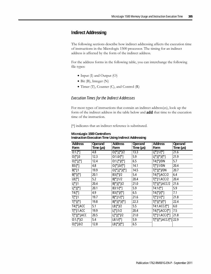
MicroLogix 1500 Memory Usage and Instruction Execution Time 385
Indirect Addressing
The following sections describe how indirect addressing affects the execution time of instructions in the Micrologix 1500 processor. The timing for an indirect address is affected by the form of the indirect address.
For the address forms in the following table, you can interchange the following file types:
• Input (I) and Output (O)• Bit (B), Integer (N)• Timer (T), Counter (C), and Control (R)
Execution Times for the Indirect Addresses
For most types of instructions that contain an indirect address(es), look up the form of the indirect address in the table below and add that time to the execution time of the instruction.
[*] indicates that an indirect reference is substituted.
MicroLogix 1500 ControllersInstruction Execution Time Using Indirect Addressing
Address Form
Operand Time (µs)
Address Form
Operand Time (µs)
Address Form
Operand Time (µs)
O:1.[*] 4.8 O:[*].[*]/2 13.3 L[*]:1/[*] 21.6O:[*].0 12.3 O:1.0/[*] 5.9 L[*]:[*]/[*] 21.9O:[*].[*] 12.4 O:1.[*]/[*] 6.5 T4:[*]/DN 5.7B3:[*] 4.8 O:[*].0/[*] 14.1 T[*]:1/DN 20.4B[*]:1 19.9 O:[*].[*]/[*] 14.5 T[*]:[*]/DN 20.7B[*]:[*] 20.1 B3:[*]/2 5.4 T4:[*].ACC/2 6.4L8:[*] 5.2 B[*]:1/2 20.4 T[*]:1.ACC/2 20.4L[*]:1 20.4 B[*]:[*]/2 21.0 T[*]:[*].ACC/2 21.6L[*]:[*] 20.1 B3:1/[*] 5.9 T4:1/[*] 5.9T4:[*] 4.9 B3:[*]/[*] 6.5 T4:[*]/[*] 7.1T[*]:1 19.7 B[*]:1/[*] 21.6 T[*]:1/[*] 21.8T[*]:[*] 19.8 B[*]:[*]/[*] 22.3 T[*]:[*]/[*] 22.4T4:[*].ACC 5.1 L8:[*]/2 5.5 T4:1.ACC/[*] 6.0T[*]:1.ACC 19.9 L[*]:1/2 20.4 T4:[*].ACC/[*] 7.5T[*]:[*].ACC 20.5 L[*]:[*]/2 21.0 T[*]:1.ACC/[*] 21.8O:1.[*]/2 5.4 L8:1/[*] 5.9 T[*]:[*].ACC/[*] 22.9O:[*].0/2 12.8 L8:[*]/[*] 6.5
Publication 1762-RM001G-EN-P - September 2011
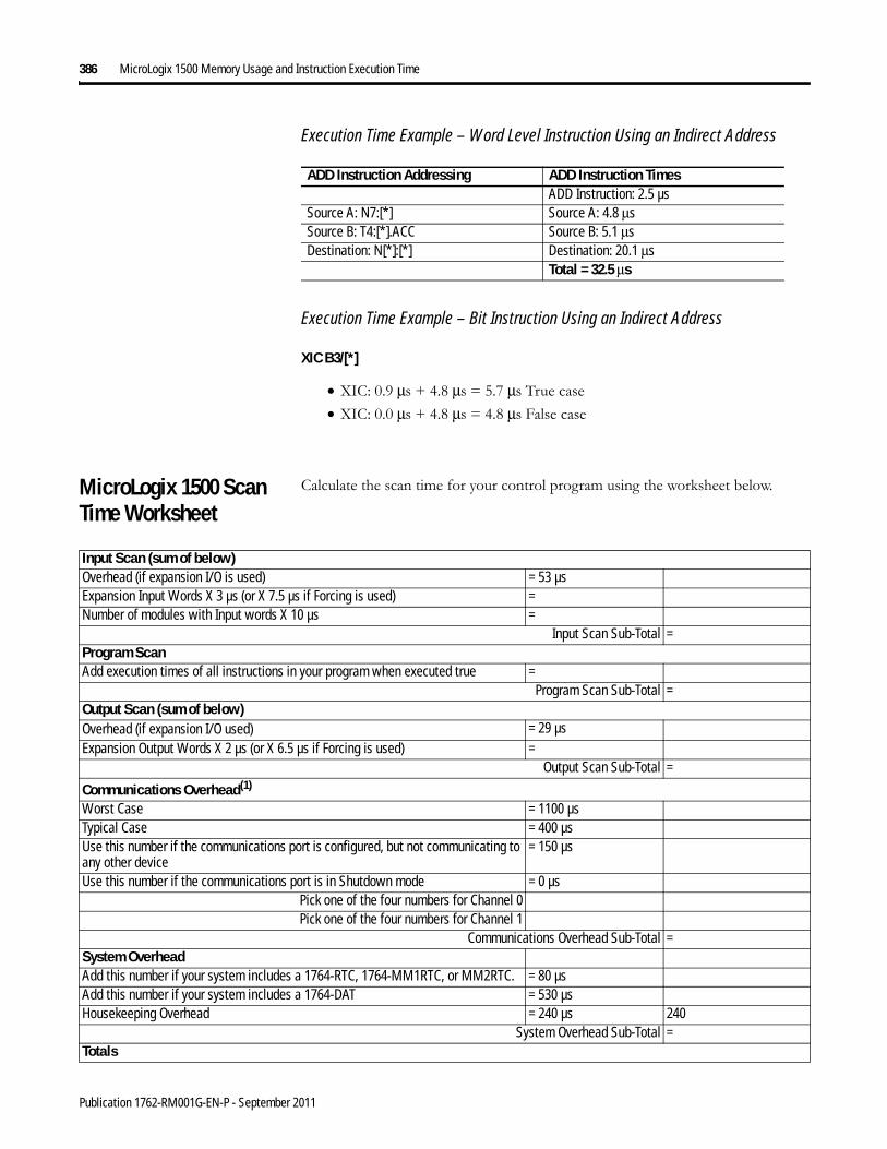
386 MicroLogix 1500 Memory Usage and Instruction Execution Time
Execution Time Example – Word Level Instruction Using an Indirect Address
Execution Time Example – Bit Instruction Using an Indirect Address
XIC B3/[*]
• XIC: 0.9 μs + 4.8 μs = 5.7 μs True case• XIC: 0.0 μs + 4.8 μs = 4.8 μs False case
MicroLogix 1500 Scan Time Worksheet
Calculate the scan time for your control program using the worksheet below.
ADD Instruction Addressing ADD Instruction TimesADD Instruction: 2.5 µs
Source A: N7:[*] Source A: 4.8 μsSource B: T4:[*].ACC Source B: 5.1 μsDestination: N[*]:[*] Destination: 20.1 μs
Total = 32.5 μs
Input Scan (sum of below)Overhead (if expansion I/O is used) = 53 µsExpansion Input Words X 3 µs (or X 7.5 µs if Forcing is used) =Number of modules with Input words X 10 µs =
Input Scan Sub-Total =Program ScanAdd execution times of all instructions in your program when executed true =
Program Scan Sub-Total =Output Scan (sum of below)Overhead (if expansion I/O used) = 29 µsExpansion Output Words X 2 µs (or X 6.5 µs if Forcing is used) =
Output Scan Sub-Total =
Communications Overhead(1)
Worst Case = 1100 µsTypical Case = 400 µsUse this number if the communications port is configured, but not communicating to any other device
= 150 µs
Use this number if the communications port is in Shutdown mode = 0 µsPick one of the four numbers for Channel 0Pick one of the four numbers for Channel 1
Communications Overhead Sub-Total =System OverheadAdd this number if your system includes a 1764-RTC, 1764-MM1RTC, or MM2RTC. = 80 µsAdd this number if your system includes a 1764-DAT = 530 µsHousekeeping Overhead = 240 µs 240
System Overhead Sub-Total =Totals
Publication 1762-RM001G-EN-P - September 2011

MicroLogix 1500 Memory Usage and Instruction Execution Time 387
Communications Multiplier Table
Sum of allMultiply by Communications Multiplier from Table X
Time Tick Multiplier (X1.02)Total Estimated Scan Time =
(1) Communications Overhead is a function of the device connected to the controller. This will not occur every scan.
Protocol
Multiplier at Various Baud Rates38.4K 19.2K 9.6K 4.8K 2.4K 1.2K 600 300 Inactive(1)
DF1 Full Duplex 1.39 1.20 1.13 1.10 1.09 1.08 1.08 1.08 1.00DF1 Half Duplex 1.18 1.12 1.09 1.08 1.07 1.07 1.06 1.06 1.01DH-485 N/A 1.14 1.10 N/A N/A N/A N/A N/A 1.06 at 19.2K
1.09 at 9.6KModbus(2) 1.21 1.12 1.09 1.08 1.08 1.08 1.08 1.08 1.00
ASCII(2) 1.52 1.33 1.24 1.20 1.19 1.18 1.18 1.17 1.00Shut Down 1.00 1.00 1.00 1.00 1.00 1.00 1.00 1.00 1.00
(1) Inactive is defined as No Messaging and No Data Monitoring. For DH-485 protocol, inactive means that the controller is not connected to a network.
(2) Applies to MicroLogix 1500 Series B Processors only.
Publication 1762-RM001G-EN-P - September 2011

388 MicroLogix 1500 Memory Usage and Instruction Execution Time
Notes:
Publication 1762-RM001G-EN-P - September 2011

Appendix C
System Status File
The status file lets you monitor how your controller works and lets you direct how you want it to work. This is done by using the status file to set up control bits and monitor both hardware and programming device faults and other status information.
Status File Overview The status file (S:) contains the following words:
IMPORTANT Do not write to reserved words in the status file. If you intend writing to status file data, it is imperative that you first understand the function fully.
Address Function PageS:0 Arithmetic Flags 390S:1 Controller Mode 391S:2 STI Mode 396S:2/9 Memory Module Program Compare 396S:2/15 Math Overflow Selection 397S:3H Watchdog Scan Time 397S:4 Free Running Clock 398S:5 Minor Error Bits 399S:6 Major Error Code 402S:7 Suspend Code 402S:8 Suspend File 402S:9 Active Nodes (Nodes 0 to 15) 403S:10 Active Nodes (Nodes 16 to 31) 403S:13, S:14 Math Register 403S:15L Node Address 404S:15H Baud Rate 404S:22 Maximum Scan Time 404S:29 User Fault Routine File Number 405S:30 STI Set Point 405S:31 STI File Number 405S:33 Channel 0 Communications 405S:35 Last 100 µSec Scan Time 407S:36/10 Data File Overwrite Protection Lost 407S:37 RTC Year 407S:38 RTC Month 408S:39 RTC Day of Month 408S:40 RTC Hours 408S:41 RTC Minutes 409
389 Publication 1762-RM001G-EN-P - September 2011
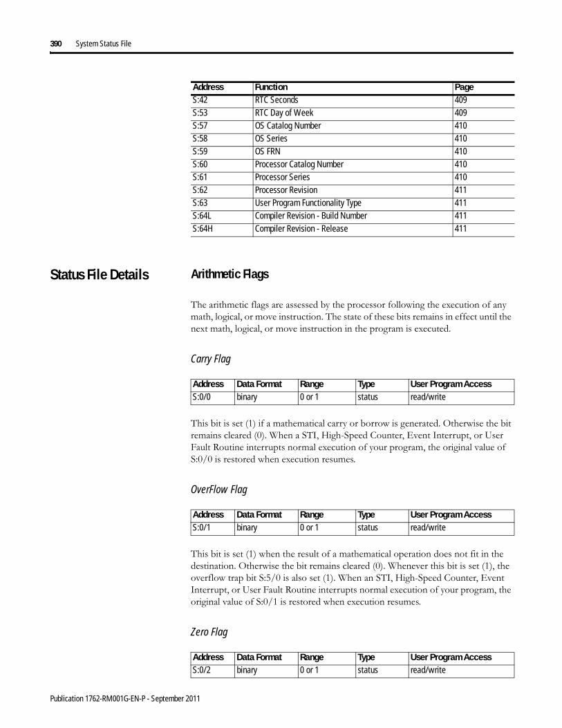
390 System Status File
Status File Details Arithmetic Flags
The arithmetic flags are assessed by the processor following the execution of any math, logical, or move instruction. The state of these bits remains in effect until the next math, logical, or move instruction in the program is executed.
Carry Flag
This bit is set (1) if a mathematical carry or borrow is generated. Otherwise the bit remains cleared (0). When a STI, High-Speed Counter, Event Interrupt, or User Fault Routine interrupts normal execution of your program, the original value of S:0/0 is restored when execution resumes.
OverFlow Flag
This bit is set (1) when the result of a mathematical operation does not fit in the destination. Otherwise the bit remains cleared (0). Whenever this bit is set (1), the overflow trap bit S:5/0 is also set (1). When an STI, High-Speed Counter, Event Interrupt, or User Fault Routine interrupts normal execution of your program, the original value of S:0/1 is restored when execution resumes.
Zero Flag
S:42 RTC Seconds 409S:53 RTC Day of Week 409S:57 OS Catalog Number 410S:58 OS Series 410S:59 OS FRN 410S:60 Processor Catalog Number 410S:61 Processor Series 410S:62 Processor Revision 411S:63 User Program Functionality Type 411S:64L Compiler Revision - Build Number 411S:64H Compiler Revision - Release 411
Address Function Page
Address Data Format Range Type User Program AccessS:0/0 binary 0 or 1 status read/write
Address Data Format Range Type User Program AccessS:0/1 binary 0 or 1 status read/write
Address Data Format Range Type User Program AccessS:0/2 binary 0 or 1 status read/write
Publication 1762-RM001G-EN-P - September 2011

System Status File 391
This bit is set (1) when the result of a mathematical operation or data handling instruction is zero. Otherwise the bit remains cleared (0). When an STI, High-Speed Counter, Event Interrupt, or User Fault Routine interrupts normal execution of your program, the original value of S:0/2 is restored when execution resumes.
Sign Flag
This bit is set (1) when the result of a mathematical operation or data handling instruction is negative. Otherwise the bit remains cleared (0). When a STI, High-Speed Counter, Event Interrupt, or User Fault Routine interrupts normal execution of your program, the original value of S:0/3 is restored when execution resumes.
Controller Mode
User Application Mode
Bits 0 through 4 function as follows:
Address Data Format Range Type User Program AccessS:0/3 binary 0 or 1 status read/write
Address Data Format Range Type User Program AccessS:1/0 to S:1/4 binary 0 to 1 1110 status read only
S:1/0 to S:1/4 Mode ID
Controller Mode Use by MicroLogix Controller(1)
S:1/4 S:1/3 S:1/2 S:1/1 S:1/0 1200 15000 0 0 0 0 0 remote download in progress • •0 0 0 0 1 1 remote program mode • •0 0 0 1 1 3 remote suspend mode (operation halted by execution
of the SUS instruction)• •
0 0 1 1 0 6 remote run mode • •0 0 1 1 1 7 remote test continuous mode • •0 1 0 0 0 8 remote test single scan mode • •1 0 0 0 0 16 download in progress N/A •1 0 0 0 1 17 program mode N/A •1 1 0 1 1 27 suspend mode (operation halted by execution of the
SUS instruction)N/A •
1 1 1 1 0 30 run mode N/A •
(1) Valid modes are indicated by the (•) symbol. N/A indicates an invalid mode for that controller.
Publication 1762-RM001G-EN-P - September 2011

392 System Status File
Forces Enabled
This bit is always set (1) by the controller to indicate that forces are enabled.
Forces Installed
This bit is set (1) by the controller to indicate that 1 or more inputs or outputs are forced. When this bit is clear, a force condition is not present within the controller.
Fault Override At Power-Up
When set (1), causes the controller to clear the Major Error Halted bit (S:1/13) at power-up. The power-up mode is determined by the controller mode switch (MicroLogix 1500 only) and the Power-Up Mode Behavior Selection bit (S:1/12).
See also:FO - Fault Override on page 62.
Startup Protection Fault
When set (1) and the controller powers up in the RUN or REM RUN mode, the controller executes the User Fault Routine prior to the execution of the first scan of your program. You have the option of clearing the Major Error Halted bit (S:1/13) to resume operation. If the User Fault Routine does not clear bit S:1/13, the controller faults and does not enter an executing mode. Program the User Fault Routine logic accordingly.
Address Data Format Range Type User Program AccessS:1/5 binary 1 status read only
Address Data Format Range Type User Program AccessS:1/6 binary 0 or 1 status read only
Address Data Format Range Type User Program AccessS:1/8 binary 0 or 1 control read only
Address Data Format Range Type User Program AccessS:1/9 binary 0 or 1 control read only
TIP When executing the startup protection fault routine, S:6 (major error fault code) contains the value 0016H.
Publication 1762-RM001G-EN-P - September 2011

System Status File 393
Load Memory Module On Error Or Default Program
For this option to work, you must set (1) this bit in the control program before downloading the program to a memory module. When this bit it set in the memory module and power is applied, the controller downloads the memory module program when the control program is corrupt or a default program exists in the controller.
The mode of the controller after the transfer takes place is determined by the controller mode switch (MicroLogix 1500 only) and the Power-Up Mode Behavior Selection bit (S:1/12).
See also:LE - Load on Error on page 62.
Load Memory Module Always
For this option to work, you must set (1) this bit in the control program before downloading the program to a memory module. When this bit is set in the memory module and power is applied, the controller downloads the memory module program.
The mode of the controller after the transfer takes place is determined by the controller mode switch (MicroLogix 1500 only) and the Power-Up Mode Behavior Selection bit (S:1/12).
See also:LA - Load Always on page 62.
Power-Up Mode Behavior
If Power-Up Mode Behavior is clear (0 = Last State), the mode at power-up is dependent upon the:
• position of the mode switch (MicroLogix 1500 only)• state of the Major Error Halted flag (S:1/13)• mode at the previous power down
Address Data Format Range Type User Program AccessS:1/10 binary 0 or 1 control read only
TIP If you clear the controller memory, the controller loads the default program.
Address Data Format Range Type User Program AccessS:1/11 binary 0 or 1 control read only
Address Data Format Range Type User Program AccessS:1/12 binary 0 or 1 control read only
Publication 1762-RM001G-EN-P - September 2011
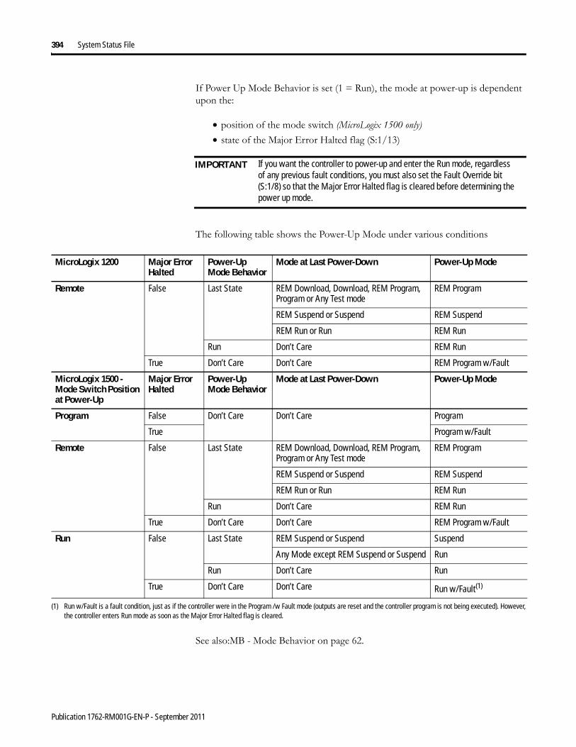
394 System Status File
If Power Up Mode Behavior is set (1 = Run), the mode at power-up is dependent upon the:
• position of the mode switch (MicroLogix 1500 only)• state of the Major Error Halted flag (S:1/13)
The following table shows the Power-Up Mode under various conditions
See also:MB - Mode Behavior on page 62.
IMPORTANT If you want the controller to power-up and enter the Run mode, regardless of any previous fault conditions, you must also set the Fault Override bit (S:1/8) so that the Major Error Halted flag is cleared before determining the power up mode.
MicroLogix 1200 Major Error Halted
Power-Up Mode Behavior
Mode at Last Power-Down Power-Up Mode
Remote False Last State REM Download, Download, REM Program, Program or Any Test mode
REM Program
REM Suspend or Suspend REM Suspend
REM Run or Run REM Run
Run Don’t Care REM Run
True Don’t Care Don’t Care REM Program w/Fault
MicroLogix 1500 - Mode Switch Position at Power-Up
Major Error Halted
Power-Up Mode Behavior
Mode at Last Power-Down Power-Up Mode
Program False Don’t Care Don’t Care Program
True Program w/Fault
Remote False Last State REM Download, Download, REM Program, Program or Any Test mode
REM Program
REM Suspend or Suspend REM Suspend
REM Run or Run REM Run
Run Don’t Care REM Run
True Don’t Care Don’t Care REM Program w/Fault
Run False Last State REM Suspend or Suspend Suspend
Any Mode except REM Suspend or Suspend Run
Run Don’t Care Run
True Don’t Care Don’t Care Run w/Fault(1)
(1) Run w/Fault is a fault condition, just as if the controller were in the Program /w Fault mode (outputs are reset and the controller program is not being executed). However, the controller enters Run mode as soon as the Major Error Halted flag is cleared.
Publication 1762-RM001G-EN-P - September 2011

System Status File 395
Major Error Halted
The controller sets (1) this bit when a major error is encountered. The controller enters a fault condition and word S:6 contains the Fault Code that can be used to diagnose the condition. Any time bit S:1/13 is set, the controller:
• turns all outputs off and flashes the FAULT LED,• or, enters the User Fault Routine allowing the control program to attempt
recovery from the fault condition. If the User Fault Routine is able to clear S:1/13 and the fault condition, the controller continues to execute the control program. If the fault cannot be cleared, the outputs are cleared and the controller exits its executing mode and the FAULT LED flashes.
Future Access (OEM Lock)
When this bit is set (1), it indicates that the programming device must have an exact copy of the controller program.
See Allow Future Access Setting (OEM Lock) on page 53 for more information.
First Scan Bit
When the controller sets (1) this bit, it indicates that the first scan of the user program is in progress (following entry into an executing mode). The controller clears this bit after the first scan..
Address Data Format Range Type User Program AccessS:1/13 binary 0 or 1 status read/write
ATTENTION: If you clear the Major Error Halted bit (S:1/13) when the controller mode switch (MicroLogix 1500 only) is in the RUN position, the controller immediately enters the RUN mode.
Address Data Format Range Type User Program AccessS:1/14 binary 0 or 1 status read only
Address Data Format Range Type User Program AccessS:1/15 binary 0 or 1 status read/write
TIP The First Scan bit (S:1/15) is set during execution of the start-up protection fault routine. Refer to S:1/9 for more information.
Publication 1762-RM001G-EN-P - September 2011

396 System Status File
STI Mode
STI Pending
This address is duplicated at STI:0/UIP. See Using the Selectable Timed Interrupt (STI) Function File on page 242 for more information.
STI Enabled
This address is duplicated at STI:0/TIE. See Using the Selectable Timed Interrupt (STI) Function File on page 242 for more information.
STI Executing
This address is duplicated at STI:0/UIX. SeeUsing the Selectable Timed Interrupt (STI) Function File on page 242 for more information.
Memory Module Program Compare
When this bit is set (1) in the controller, its user program and the memory module user program must match for the controller to enter an executing mode.
If the user program does not match the memory module program, or if the memory module is not present, the controller faults with error code 0017H on any attempt to enter an executing mode.
Address(1)
(1) This bit can only be accessed via ladder logic. It cannot be accessed via communications (such as a Message instruction from another device).
Data Format Range Type User Program Access
S:2/0 binary 0 or 1 status read only
Address(1)
(1) This bit can only be accessed via ladder logic. It cannot be accessed via communications (such as a Message instruction from another device).
Data Format Range Type User Program Access
S:2/1 binary 0 or 1 control read/write
Address(1)
(1) This bit can only be accessed via ladder logic. It cannot be accessed via communications (such as a Message instruction from another device).
Data Format Range Type User Program Access
S:2/2 binary 0 or 1 control read only
Address Data Format Range Type User Program AccessS:2/9 binary 0 or 1 control read only
Publication 1762-RM001G-EN-P - September 2011

System Status File 397
An RTC module does not support program compare. If program compare is enabled and an RTC-only module is installed, the controller does not enter an executing mode.
See also:LPC - Load Program Compare on page 62.
Math Overflow Selection
Set (1) this bit when you intend to use 32-bit addition and subtraction. When S:2/14 is set, and the result of an ADD, SUB, MUL, or DIV instruction cannot be represented in the destination address (underflow or overflow),
• the overflow bit S:0/1 is set,• the overflow trap bit S:5/0 is set, • and the destination address contains the unsigned truncated least significant
16 or 32 bits of the result.
The default condition of S:2/14 is cleared (0). When S:2/14 is cleared (0), and the result of an ADD, SUB, MUL, or DIV instruction cannot be represented in the destination address (underflow or overflow),
• the overflow bit S:0/1 is set,• the overflow trap bit S:5/0 is set, • the destination address contains +32,767 (word) or +2,147,483,647 (long
word) if the result is positive; or -32,768 (word) or -2,147,483,648 (long word) if the result is negative.
To provide protection from inadvertent alteration of your selection, program an unconditional OTL instruction at address S:2/14 to ensure the new math overflow operation. Program an unconditional OTU instruction at address S:2/14 to ensure the original math overflow operation.
Watchdog Scan Time
This byte value contains the number of 10 ms intervals allowed to occur during a program cycle. The timing accuracy is from -10 ms to +0 ms. This means that a value of 2 results in a timeout between 10 and 20 ms.
Address Data Format Range Type User Program AccessS:2/14 binary 0 or 1 control read/write
Address Data Format Range Type User Program AccessS:3H Byte 2 to 255 control read/write
Publication 1762-RM001G-EN-P - September 2011
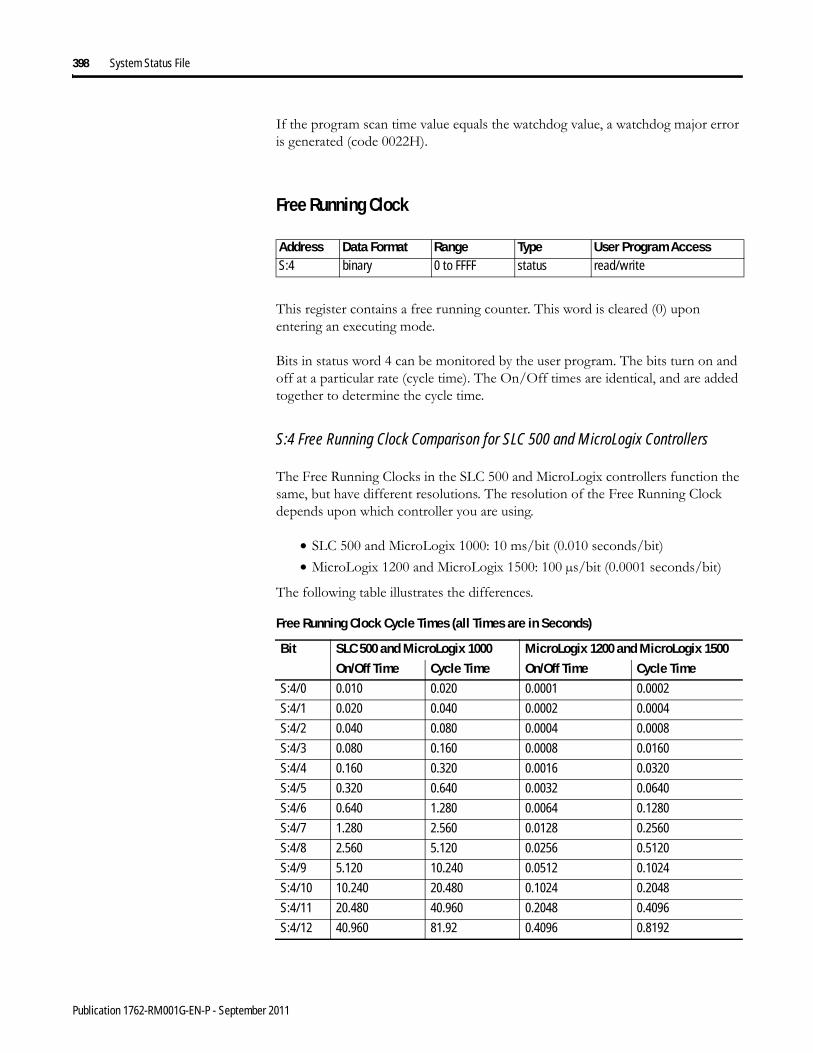
398 System Status File
If the program scan time value equals the watchdog value, a watchdog major error is generated (code 0022H).
Free Running Clock
This register contains a free running counter. This word is cleared (0) upon entering an executing mode.
Bits in status word 4 can be monitored by the user program. The bits turn on and off at a particular rate (cycle time). The On/Off times are identical, and are added together to determine the cycle time.
S:4 Free Running Clock Comparison for SLC 500 and MicroLogix Controllers
The Free Running Clocks in the SLC 500 and MicroLogix controllers function the same, but have different resolutions. The resolution of the Free Running Clock depends upon which controller you are using.
• SLC 500 and MicroLogix 1000: 10 ms/bit (0.010 seconds/bit)• MicroLogix 1200 and MicroLogix 1500: 100 µs/bit (0.0001 seconds/bit)
The following table illustrates the differences.
Address Data Format Range Type User Program AccessS:4 binary 0 to FFFF status read/write
Free Running Clock Cycle Times (all Times are in Seconds)
Bit SLC 500 and MicroLogix 1000 MicroLogix 1200 and MicroLogix 1500On/Off Time Cycle Time On/Off Time Cycle Time
S:4/0 0.010 0.020 0.0001 0.0002
S:4/1 0.020 0.040 0.0002 0.0004
S:4/2 0.040 0.080 0.0004 0.0008
S:4/3 0.080 0.160 0.0008 0.0160
S:4/4 0.160 0.320 0.0016 0.0320
S:4/5 0.320 0.640 0.0032 0.0640
S:4/6 0.640 1.280 0.0064 0.1280
S:4/7 1.280 2.560 0.0128 0.2560
S:4/8 2.560 5.120 0.0256 0.5120
S:4/9 5.120 10.240 0.0512 0.1024
S:4/10 10.240 20.480 0.1024 0.2048
S:4/11 20.480 40.960 0.2048 0.4096
S:4/12 40.960 81.92 0.4096 0.8192
Publication 1762-RM001G-EN-P - September 2011
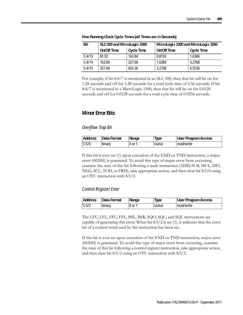
System Status File 399
For example, if bit S:4/7 is monitored in an SLC 500, then that bit will be on for 1.28 seconds and off for 1.28 seconds for a total cycle time of 2.56 seconds. If bit S:4/7 is monitored in a MicroLogix 1500, then that bit will be on for 0.0128 seconds and off for 0.0128 seconds for a total cycle time of 0.0256 seconds.
Minor Error Bits
Overflow Trap Bit
If this bit is ever set (1) upon execution of the END or TND instruction, a major error (0020H) is generated. To avoid this type of major error from occurring, examine the state of this bit following a math instruction (ADD, SUB, MUL, DIV, NEG, SCL, TOD, or FRD), take appropriate action, and then clear bit S:5/0 using an OTU instruction with S:5/0.
Control Register Error
The LFU, LFL, FFU, FFL, BSL, BSR, SQO, SQC, and SQL instructions are capable of generating this error. When bit S:5/2 is set (1), it indicates that the error bit of a control word used by the instruction has been set.
If this bit is ever set upon execution of the END or TND instruction, major error (0020H) is generated. To avoid this type of major error from occurring, examine the state of this bit following a control register instruction, take appropriate action, and then clear bit S:5/2 using an OTU instruction with S:5/2.
S:4/13 81.92 163.84 0.8192 1.6384
S:4/14 163.84 327.68 1.6384 3.2768
S:4/15 327.68 655.36 3.2768 6.5536
Address Data Format Range Type User Program AccessS:5/0 binary 0 or 1 status read/write
Address Data Format Range Type User Program AccessS:5/2 binary 0 or 1 status read/write
Free Running Clock Cycle Times (all Times are in Seconds)
Bit SLC 500 and MicroLogix 1000 MicroLogix 1200 and MicroLogix 1500On/Off Time Cycle Time On/Off Time Cycle Time
Publication 1762-RM001G-EN-P - September 2011

400 System Status File
Major Error Detected in User Fault Routine
When set (1), the major error code (S:6) represents the major error that occurred while processing the User Fault Routine due to another major error.
Memory Module Boot
When this bit is set (1) by the controller, it indicates that a memory module program has been transferred due to S:1/10 (Load Memory Module on Error or Default Program) or S:1/11 (Load Memory Module Always) being set in an attached memory module user program. This bit is not cleared(0) by the controller.
Your program can examine the state of this bit on the first scan (using bit S:1/15) on entry into an Executing mode to determine if the memory module user program has been transferred after a power-up occurred. This information is useful when you have an application that contains retentive data and a memory module has bit S:1/10 or bit S:1/11 set.
Memory Module Password Mismatch
At power-up, if Load Always is set, and the controller and memory module passwords do not match, the Memory Module Password Mismatch bit is set (1).
SeePassword Protection on page 52 for more information.
STI Lost
This address is duplicated at STI:0/UIL. SeeUsing the Selectable Timed Interrupt (STI) Function File on page 242 for more information.
Address Data Format Range Type User Program AccessS:5/3 binary 0 or 1 status read/write
Address Data Format Range Type User Program AccessS:5/8 binary 0 or 1 status read/write
Address Data Format Range Type User Program AccessS:5/9 binary 0 or 1 status read/write
Address(1)
(1) This bit can only be accessed via ladder logic. It cannot be accessed via communications (such as a Message instruction from another device).
Data Format Range Type User Program Access
S:5/10 binary 0 or 1 status read/write
Publication 1762-RM001G-EN-P - September 2011

System Status File 401
Retentive Data Lost (MicroLogix 1200 only)
This bit is set (1) whenever retentive data is lost. This bit remains set until you clear (0) it. The controller validates retentive data at power up. If user data is invalid, the controller sets the Retentive Data Lost indicator. The data in the controller are the values that were in the program when the program was last transferred to the controller. If the Retentive Data Lost bit is set, a fault occurs when entering an executing mode, but only if the Fault Override bit (S:1/8) is not set.
Processor Battery Low (MicroLogix 1500 only)
This bit is set (1) when the battery is low.
See also: RTC Battery Operation on page 58.
Input Filter Selection Modified
This bit is set (1) whenever the discrete input filter selection in the control program is not compatible with the hardware.
ASCII String Manipulation Error
This bit is set (1) whenever an invalid string length occurs. When S:5/15 is set, the Invalid String Length Error (1F39H) is written to the Major Error Fault Code word (S:6).
This bit applies to the MicroLogix 1200 and 1500 Series B Controllers.
Address Data Format Range Type User Program AccessS:5/11 binary 0 or 1 status read/write
Address Data Format Range Type User Program AccessS:5/11 binary 0 or 1 status read only
IMPORTANT Install a replacement battery immediately. See your hardware manual for more information.
Address Data Format Range Type User Program AccessS:5/13 binary 0 or 1 status read/write
Address Data Format Range Type User Program AccessS:5/15 binary 0 or 1 status read
Publication 1762-RM001G-EN-P - September 2011

402 System Status File
Major Error Code
This register displays a value which can be used to determine what caused a fault to occur. SeeIdentifying Controller Faults on page 413 to learn more about troubleshooting faults.
Suspend Code
When the controller executes an Suspend (SUS) instruction, the SUS code is written to this location, S:7. This pinpoints the conditions in the application that caused the Suspend mode. The controller does not clear this value.
Use the SUS instruction with startup troubleshooting, or as runtime diagnostics for detection of system errors.
Suspend File
When the controller executes an Suspend (SUS) instruction, the SUS file is written to this location, S:8. This pinpoints the conditions in the application that caused the Suspend mode. The controller does not clear this value.
Use the SUS instruction with startup troubleshooting, or as runtime diagnostics for detection of system errors.
Address Data Format Range Type User Program AccessS:6 word 0 to FFFF status read/write
Address Data Format Range Type User Program AccessS:7 word -32,768 to
+32,767status read/write
Address Data Format Range Type User Program AccessS:8 word 0 to 255 status read/write
Publication 1762-RM001G-EN-P - September 2011
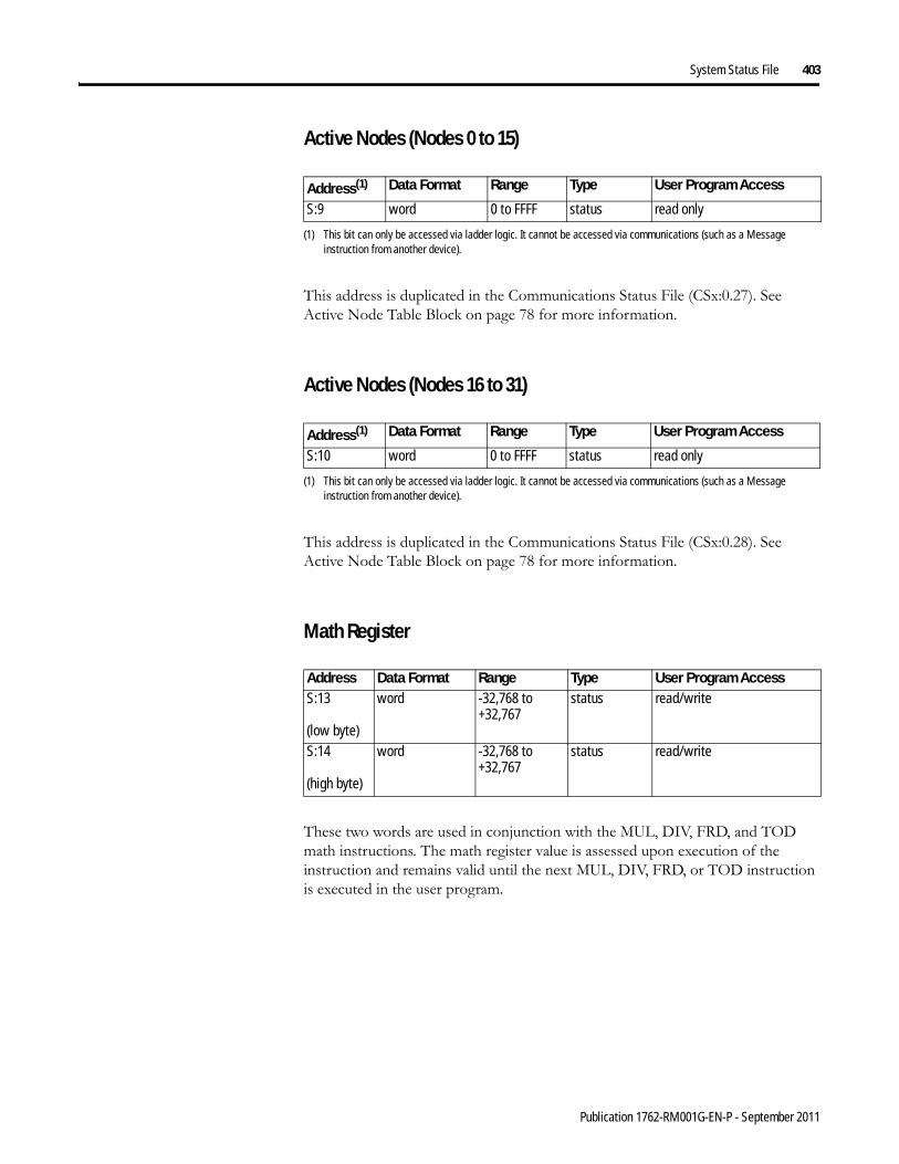
System Status File 403
Active Nodes (Nodes 0 to 15)
This address is duplicated in the Communications Status File (CSx:0.27). See Active Node Table Block on page 78 for more information.
Active Nodes (Nodes 16 to 31)
This address is duplicated in the Communications Status File (CSx:0.28). See Active Node Table Block on page 78 for more information.
Math Register
These two words are used in conjunction with the MUL, DIV, FRD, and TOD math instructions. The math register value is assessed upon execution of the instruction and remains valid until the next MUL, DIV, FRD, or TOD instruction is executed in the user program.
Address(1)
(1) This bit can only be accessed via ladder logic. It cannot be accessed via communications (such as a Message instruction from another device).
Data Format Range Type User Program Access
S:9 word 0 to FFFF status read only
Address(1)
(1) This bit can only be accessed via ladder logic. It cannot be accessed via communications (such as a Message instruction from another device).
Data Format Range Type User Program Access
S:10 word 0 to FFFF status read only
Address Data Format Range Type User Program AccessS:13
(low byte)
word -32,768 to +32,767
status read/write
S:14
(high byte)
word -32,768 to +32,767
status read/write
Publication 1762-RM001G-EN-P - September 2011
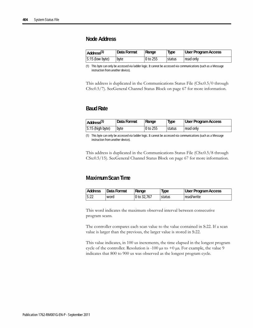
404 System Status File
Node Address
This address is duplicated in the Communications Status File (CSx:0.5/0 through CSx:0.5/7). SeeGeneral Channel Status Block on page 67 for more information.
Baud Rate
This address is duplicated in the Communications Status File (CSx:0.5/8 through CSx:0.5/15). SeeGeneral Channel Status Block on page 67 for more information.
Maximum Scan Time
This word indicates the maximum observed interval between consecutive program scans.
The controller compares each scan value to the value contained in S:22. If a scan value is larger than the previous, the larger value is stored in S:22.
This value indicates, in 100 us increments, the time elapsed in the longest program cycle of the controller. Resolution is -100 µs to +0 µs. For example, the value 9 indicates that 800 to 900 us was observed as the longest program cycle.
Address(1)
(1) This byte can only be accessed via ladder logic. It cannot be accessed via communications (such as a Message instruction from another device).
Data Format Range Type User Program Access
S:15 (low byte) byte 0 to 255 status read only
Address(1)
(1) This byte can only be accessed via ladder logic. It cannot be accessed via communications (such as a Message instruction from another device).
Data Format Range Type User Program Access
S:15 (high byte) byte 0 to 255 status read only
Address Data Format Range Type User Program AccessS:22 word 0 to 32,767 status read/write
Publication 1762-RM001G-EN-P - September 2011

System Status File 405
User Fault Routine File Number
This register is used to control which subroutine executes when a User Fault is generated.
STI Set Point
This address is duplicated at STI:0/SPM. SeeUsing the Selectable Timed Interrupt (STI) Function File on page 242 for more information.
STI File Number
This address is duplicated at STI:0/PFN. SeeUsing the Selectable Timed Interrupt (STI) Function File on page 242 for more information.
Channel 0 Communications
Incoming Command Pending
This address is duplicated in the Communications Status File at CS0:0.4/0. See General Channel Status Block on page 67 for more information.
Address Data Format Range Type User Program AccessS:29 word 0 to 255 status read only
Address(1)
(1) This bit can only be accessed via ladder logic. It cannot be accessed via communications (such as a Message instruction from another device).
Data Format Range Type User Program Access
S:30 word 0 to 65535 status read only
Address(1)
(1) This bit can only be accessed via ladder logic. It cannot be accessed via communications (such as a Message instruction from another device).
Data Format Range Type User Program Access
S:31 word 0 to 65535 status read only
Address(1)
(1) This bit can only be accessed via ladder logic. It cannot be accessed via communications (such as a Message instruction from another device).
Data Format Range Type User Program Access
S:33/0 binary 0 or 1 status read only
Publication 1762-RM001G-EN-P - September 2011

406 System Status File
Message Reply Pending
This address is duplicated in the Communications Status File at CS0:0.4/1. See General Channel Status Block on page 67 for more information.
Outgoing Message Command Pending
This address is duplicated in the Communications Status File at CS0:0.4/2. See General Channel Status Block on page 67 for more information.
Communications Mode Selection
This address is duplicated in the Communications Status File at CS0:0.4/3. See General Channel Status Block on page 67 for more information.
Communications Active
This address is duplicated in the Communications Status File at CS0:0.4/4. See General Channel Status Block on page 67 for more information.
Address(1)
(1) This bit can only be accessed via ladder logic. It cannot be accessed via communications (such as a Message instruction from another device).
Data Format Range Type User Program Access
S:33/1 binary 0 or 1 status read only
Address(1)
(1) This bit can only be accessed via ladder logic. It cannot be accessed via communications (such as a Message instruction from another device).
Data Format Range Type User Program Access
S:33/2 binary 0 or 1 status read only
Address(1)
(1) This bit can only be accessed via ladder logic. It cannot be accessed via communications (such as a Message instruction from another device).
Data Format Range Type User Program Access
S:33/3 binary 0 or 1 status read only
Address(1)
(1) This bit can only be accessed via ladder logic. It cannot be accessed via communications (such as a Message instruction from another device).
Data Format Range Type User Program Access
S:33/4 binary 0 or 1 status read only
Publication 1762-RM001G-EN-P - September 2011
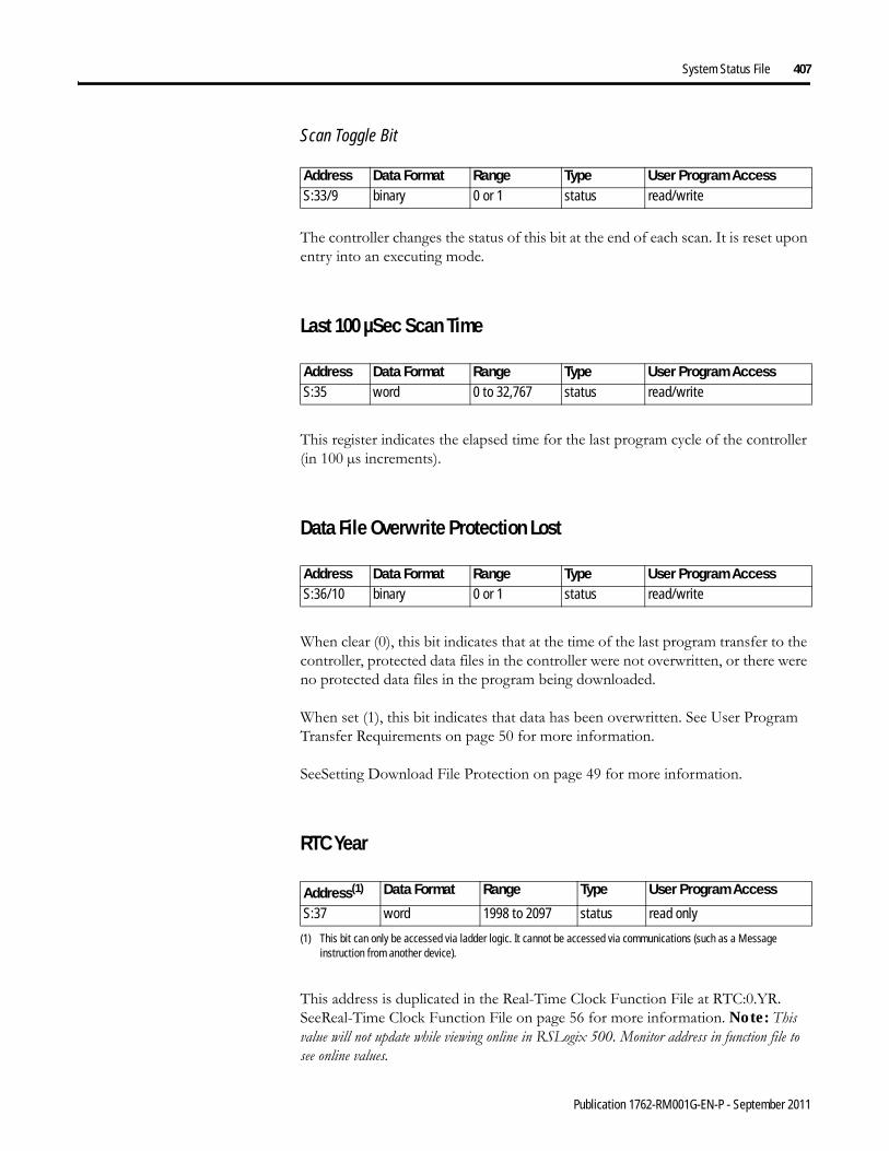
System Status File 407
Scan Toggle Bit
The controller changes the status of this bit at the end of each scan. It is reset upon entry into an executing mode.
Last 100 µSec Scan Time
This register indicates the elapsed time for the last program cycle of the controller (in 100 µs increments).
Data File Overwrite Protection Lost
When clear (0), this bit indicates that at the time of the last program transfer to the controller, protected data files in the controller were not overwritten, or there were no protected data files in the program being downloaded.
When set (1), this bit indicates that data has been overwritten. See User Program Transfer Requirements on page 50 for more information.
SeeSetting Download File Protection on page 49 for more information.
RTC Year
This address is duplicated in the Real-Time Clock Function File at RTC:0.YR. SeeReal-Time Clock Function File on page 56 for more information. Note: This value will not update while viewing online in RSLogix 500. Monitor address in function file to see online values.
Address Data Format Range Type User Program AccessS:33/9 binary 0 or 1 status read/write
Address Data Format Range Type User Program AccessS:35 word 0 to 32,767 status read/write
Address Data Format Range Type User Program AccessS:36/10 binary 0 or 1 status read/write
Address(1)
(1) This bit can only be accessed via ladder logic. It cannot be accessed via communications (such as a Message instruction from another device).
Data Format Range Type User Program Access
S:37 word 1998 to 2097 status read only
Publication 1762-RM001G-EN-P - September 2011

408 System Status File
RTC Month
This address is duplicated in the Real-Time Clock Function File at RTC:0.MON. SeeReal-Time Clock Function File on page 56 for more information. Note: This value will not update while viewing online in RSLogix 500. Monitor address in function file to see online values.
RTC Day of Month
This address is duplicated in the Real-Time Clock Function File at RTC:0.DAY. SeeReal-Time Clock Function File on page 56 for more information. Note: This value will not update while viewing online in RSLogix 500. Monitor address in function file to see online values.
RTC Hours
This address is duplicated in the Real-Time Clock Function File at RTC:0.HR. SeeReal-Time Clock Function File on page 56 for more information. Note: This value will not update while viewing online in RSLogix 500. Monitor address in function file to see online values.
Address(1)
(1) This bit can only be accessed via ladder logic. It cannot be accessed via communications (such as a Message instruction from another device).
Data Format Range Type User Program Access
S:38 word 1 to 12 status read only
Address(1)
(1) This bit can only be accessed via ladder logic. It cannot be accessed via communications (such as a Message instruction from another device).
Data Format Range Type User Program Access
S:39 word 1 to 31 status read only
Address(1)
(1) This word can only be accessed via ladder logic. It cannot be accessed via communications (such as a Message instruction from another device).
Data Format Range Type User Program Access
S:40 word 0 to 23 status read only
Publication 1762-RM001G-EN-P - September 2011

System Status File 409
RTC Minutes
This address is duplicated in the Real-Time Clock Function File at RTC:0.MIN. SeeReal-Time Clock Function File on page 56 for more information. Note: This value will not update while viewing online in RSLogix 500. Monitor address in function file to see online values.
RTC Seconds
This address is duplicated in the Real-Time Clock Function File at RTC:0.SEC. SeeReal-Time Clock Function File on page 56 for more information. Note: This value will not update while viewing online in RSLogix 500. Monitor address in function file to see online values.
RTC Day of Week
This address is duplicated in the Real-Time Clock Function File at RTC:0.DOW. SeeReal-Time Clock Function File on page 56 for more information. Note: This value will not update while viewing online in RSLogix 500. Monitor address in function file to see online values.
Address(1)
(1) This word can only be accessed via ladder logic. It cannot be accessed via communications (such as a Message instruction from another device).
Data Format Range Type User Program Access
S:41 word 0 to 59 status read only
Address(1)
(1) This word can only be accessed via ladder logic. It cannot be accessed via communications (such as a Message instruction from another device).
Data Format Range Type User Program Access
S:42 word 0 to 59 status read only
Address(1)
(1) This word can only be accessed via ladder logic. It cannot be accessed via communications (such as a Message instruction from another device).
Data Format Range Type User Program Access
S:53 word 0 to 6 status read only
Publication 1762-RM001G-EN-P - September 2011
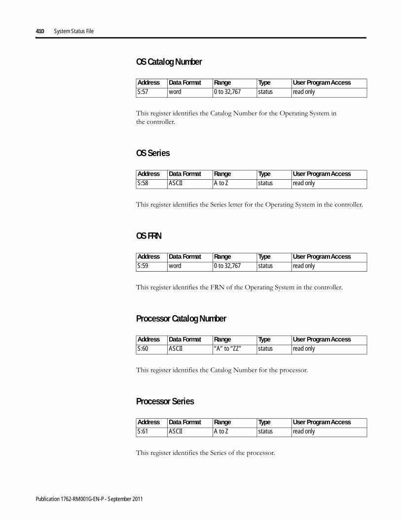
410 System Status File
OS Catalog Number
This register identifies the Catalog Number for the Operating System in the controller.
OS Series
This register identifies the Series letter for the Operating System in the controller.
OS FRN
This register identifies the FRN of the Operating System in the controller.
Processor Catalog Number
This register identifies the Catalog Number for the processor.
Processor Series
This register identifies the Series of the processor.
Address Data Format Range Type User Program AccessS:57 word 0 to 32,767 status read only
Address Data Format Range Type User Program AccessS:58 ASCII A to Z status read only
Address Data Format Range Type User Program AccessS:59 word 0 to 32,767 status read only
Address Data Format Range Type User Program AccessS:60 ASCII “A” to “ZZ” status read only
Address Data Format Range Type User Program AccessS:61 ASCII A to Z status read only
Publication 1762-RM001G-EN-P - September 2011
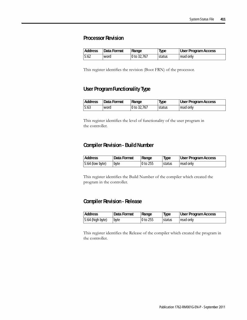
System Status File 411
Processor Revision
This register identifies the revision (Boot FRN) of the processor.
User Program Functionality Type
This register identifies the level of functionality of the user program in the controller.
Compiler Revision - Build Number
This register identifies the Build Number of the compiler which created the program in the controller.
Compiler Revision - Release
This register identifies the Release of the compiler which created the program in the controller.
Address Data Format Range Type User Program AccessS:62 word 0 to 32,767 status read only
Address Data Format Range Type User Program AccessS:63 word 0 to 32,767 status read only
Address Data Format Range Type User Program AccessS:64 (low byte) byte 0 to 255 status read only
Address Data Format Range Type User Program AccessS:64 (high byte) byte 0 to 255 status read only
Publication 1762-RM001G-EN-P - September 2011

412 System Status File
Notes:
Publication 1762-RM001G-EN-P - September 2011

Appendix D
Fault Messages and Error Codes
This chapter describes how to troubleshoot your controller. Topics include:
• identifying controller faults• contacting Rockwell Automation for assistance
Identifying Controller Faults
While a program is executing, a fault may occur within the operating system or your program. When a fault occurs, you have various options to determine what the fault is and how to correct it. This section describes how to clear faults and provides a list of possible advisory messages with recommended corrective actions.
Automatically Clearing Faults
You can automatically clear a fault by cycling power to the controller when the Fault Override at Power-Up bit (S:1/8) is set in the status file.
You can also configure the controller to clear faults and go to RUN every time the controller is power cycled. This is a feature that OEMs can build into their equipment to allow end users to reset the controller. If the controller faults, it can be reset by simply cycling power to the machine. To accomplish this, set the following bits in the status file:
• S2:1/8 - Fault Override at Power-up• S2:1/12 - Mode Behavior
If the fault condition still exists after cycling power, the controller re-enters the fault mode. For more information on status bits, see System Status File on page 389.
TIP You can declare your own application-specific major fault by writing your own unique value to S:6 and then setting bit S:1/13 to prevent reusing system defined codes. The recommended values for user-defined faults are FF00 to FF0F.
413 Publication 1762-RM001G-EN-P - September 2011

414 Fault Messages and Error Codes
Manually Clearing Faults Using the Fault Routine
The occurrence of recoverable or non-recoverable user faults can cause the user fault subroutine to be executed. If the fault is recoverable, the subroutine can be used to correct the problem and clear the fault bit S:1/13. The controller then continues in the Run or test mode.
The subroutine does not execute for non-user faults. See User Fault Routine on page 236 for information on creating a user fault subroutine.
Fault Messages
This section contains fault messages that can occur during operation of the MicroLogix 1200 and MicroLogix 1500 programmable controllers. Each table lists the error code description, the probable cause, and the recommended corrective action.
Error Code (Hex)
Advisory Message Description Fault Classification
Recommended Action
0001 NVRAM ERROR The default program is loaded to the controller memory. This occurs:
• if a power down occurred during program download or transfer from the memory module.
• RAM integrity test failed.
• FLASH integrity test failed (MicroLogix 1200 only).
Non-User • Re-download or transfer the program.
• Verify battery is connected (MicroLogix 1500 only).
• Contact your local Rockwell Automation representative if the error persists.
0002 UNEXPECTED RESET • The controller was unexpectedly reset due to a noisy environment or internal hardware failure.
• The default program is loaded. (MicroLogix 1500 only)
• Retentive Data is lost. See page 401. (MicroLogix 1200 only)
Non-User • Refer to proper grounding guidelines and using surge suppressors in your controller’s User Manual.
• Verify battery is connected (MicroLogix 1500 only).
• Contact your local Rockwell Automation representative if the error persists.
0003 MEMORY MODULE USER PROGRAM IS CORRUPT
Memory module memory error. This error can also occur when going to the Run mode.
Non-User Re-program the memory module. If the error persists, replace the memory module.
0004 MEMORY INTEGRITY ERROR
While the controller was powered up, ROM or RAM became corrupt.
Non-User • Cycle power on your unit. Then, re-download your program and start up your system.
• Refer to proper grounding guidelines and using surge suppressors in your controller’s User Manual.
• Contact your local Rockwell Automation representative if the error persists.
Publication 1762-RM001G-EN-P - September 2011
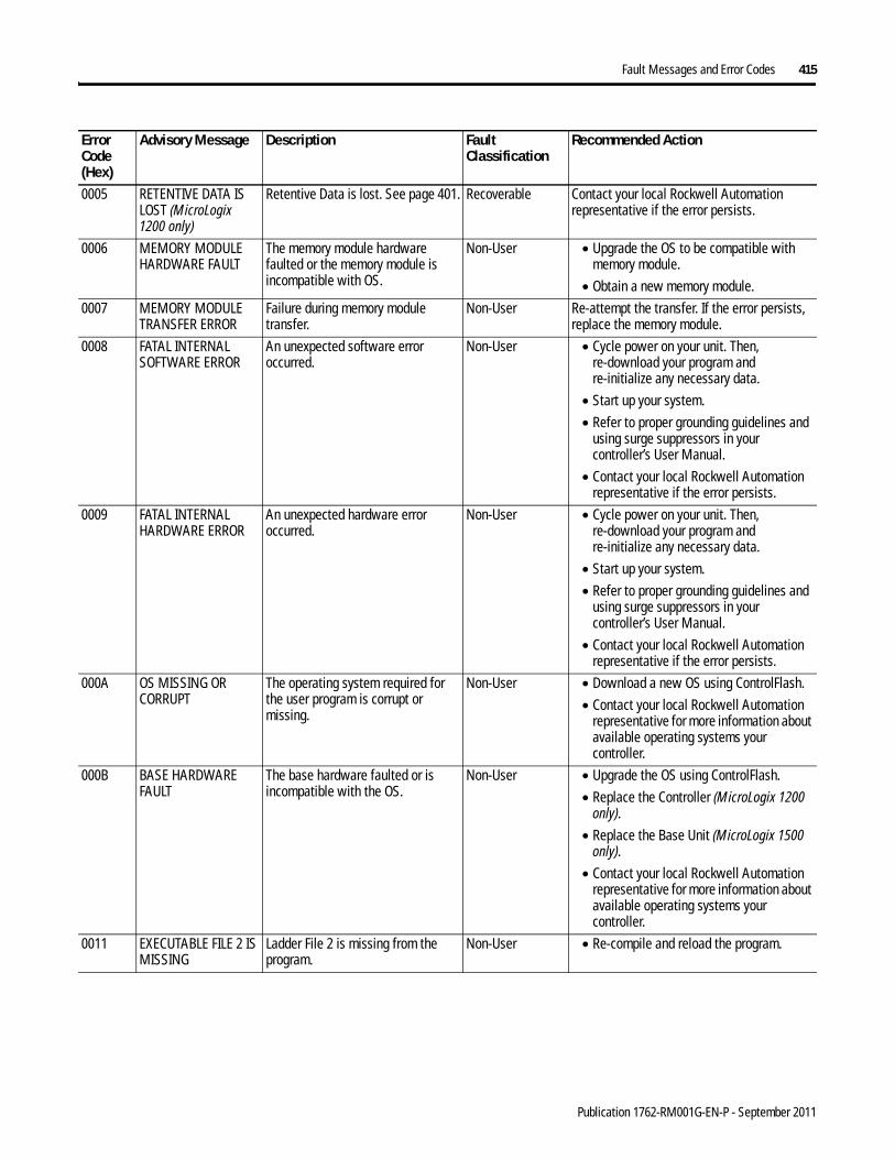
Fault Messages and Error Codes 415
0005 RETENTIVE DATA IS LOST (MicroLogix 1200 only)
Retentive Data is lost. See page 401. Recoverable Contact your local Rockwell Automation representative if the error persists.
0006 MEMORY MODULE HARDWARE FAULT
The memory module hardware faulted or the memory module is incompatible with OS.
Non-User • Upgrade the OS to be compatible with memory module.
• Obtain a new memory module.
0007 MEMORY MODULE TRANSFER ERROR
Failure during memory module transfer.
Non-User Re-attempt the transfer. If the error persists, replace the memory module.
0008 FATAL INTERNAL SOFTWARE ERROR
An unexpected software error occurred.
Non-User • Cycle power on your unit. Then, re-download your program and re-initialize any necessary data.
• Start up your system.
• Refer to proper grounding guidelines and using surge suppressors in your controller’s User Manual.
• Contact your local Rockwell Automation representative if the error persists.
0009 FATAL INTERNAL HARDWARE ERROR
An unexpected hardware error occurred.
Non-User • Cycle power on your unit. Then, re-download your program and re-initialize any necessary data.
• Start up your system.
• Refer to proper grounding guidelines and using surge suppressors in your controller’s User Manual.
• Contact your local Rockwell Automation representative if the error persists.
000A OS MISSING OR CORRUPT
The operating system required for the user program is corrupt or missing.
Non-User • Download a new OS using ControlFlash.
• Contact your local Rockwell Automation representative for more information about available operating systems your controller.
000B BASE HARDWARE FAULT
The base hardware faulted or is incompatible with the OS.
Non-User • Upgrade the OS using ControlFlash.
• Replace the Controller (MicroLogix 1200 only).
• Replace the Base Unit (MicroLogix 1500 only).
• Contact your local Rockwell Automation representative for more information about available operating systems your controller.
0011 EXECUTABLE FILE 2 IS MISSING
Ladder File 2 is missing from the program.
Non-User • Re-compile and reload the program.
Error Code (Hex)
Advisory Message Description Fault Classification
Recommended Action
Publication 1762-RM001G-EN-P - September 2011
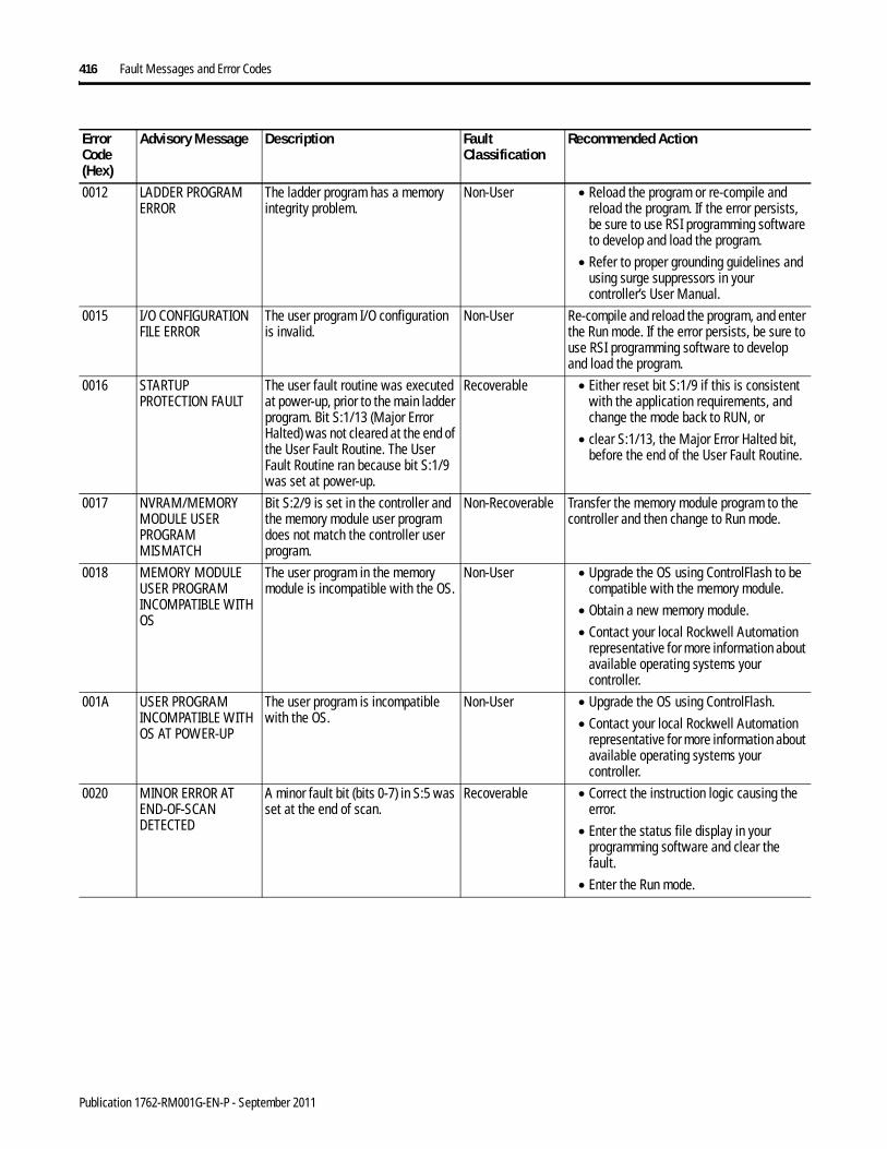
416 Fault Messages and Error Codes
0012 LADDER PROGRAM ERROR
The ladder program has a memory integrity problem.
Non-User • Reload the program or re-compile and reload the program. If the error persists, be sure to use RSI programming software to develop and load the program.
• Refer to proper grounding guidelines and using surge suppressors in your controller’s User Manual.
0015 I/O CONFIGURATION FILE ERROR
The user program I/O configuration is invalid.
Non-User Re-compile and reload the program, and enter the Run mode. If the error persists, be sure to use RSI programming software to develop and load the program.
0016 STARTUP PROTECTION FAULT
The user fault routine was executed at power-up, prior to the main ladder program. Bit S:1/13 (Major Error Halted) was not cleared at the end of the User Fault Routine. The User Fault Routine ran because bit S:1/9 was set at power-up.
Recoverable • Either reset bit S:1/9 if this is consistent with the application requirements, and change the mode back to RUN, or
• clear S:1/13, the Major Error Halted bit, before the end of the User Fault Routine.
0017 NVRAM/MEMORY MODULE USER PROGRAM MISMATCH
Bit S:2/9 is set in the controller and the memory module user program does not match the controller user program.
Non-Recoverable Transfer the memory module program to the controller and then change to Run mode.
0018 MEMORY MODULE USER PROGRAM INCOMPATIBLE WITH OS
The user program in the memory module is incompatible with the OS.
Non-User • Upgrade the OS using ControlFlash to be compatible with the memory module.
• Obtain a new memory module.
• Contact your local Rockwell Automation representative for more information about available operating systems your controller.
001A USER PROGRAM INCOMPATIBLE WITH OS AT POWER-UP
The user program is incompatible with the OS.
Non-User • Upgrade the OS using ControlFlash.
• Contact your local Rockwell Automation representative for more information about available operating systems your controller.
0020 MINOR ERROR AT END-OF-SCAN DETECTED
A minor fault bit (bits 0-7) in S:5 was set at the end of scan.
Recoverable • Correct the instruction logic causing the error.
• Enter the status file display in your programming software and clear the fault.
• Enter the Run mode.
Error Code (Hex)
Advisory Message Description Fault Classification
Recommended Action
Publication 1762-RM001G-EN-P - September 2011
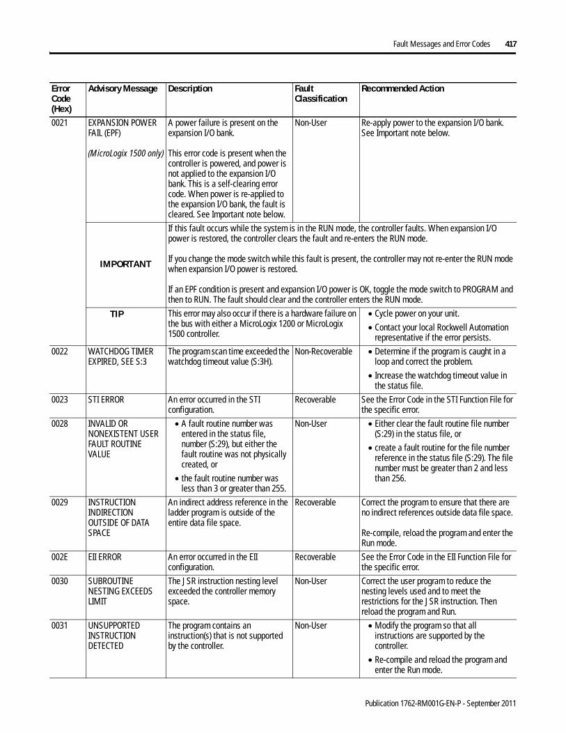
Fault Messages and Error Codes 417
0021 EXPANSION POWER FAIL (EPF)
(MicroLogix 1500 only)
A power failure is present on the expansion I/O bank.
This error code is present when the controller is powered, and power is not applied to the expansion I/O bank. This is a self-clearing error code. When power is re-applied to the expansion I/O bank, the fault is cleared. See Important note below.
Non-User Re-apply power to the expansion I/O bank. See Important note below.
IMPORTANT
If this fault occurs while the system is in the RUN mode, the controller faults. When expansion I/O power is restored, the controller clears the fault and re-enters the RUN mode.
If you change the mode switch while this fault is present, the controller may not re-enter the RUN mode when expansion I/O power is restored.
If an EPF condition is present and expansion I/O power is OK, toggle the mode switch to PROGRAM and then to RUN. The fault should clear and the controller enters the RUN mode.
TIP This error may also occur if there is a hardware failure on the bus with either a MicroLogix 1200 or MicroLogix 1500 controller.
• Cycle power on your unit.
• Contact your local Rockwell Automation representative if the error persists.
0022 WATCHDOG TIMER EXPIRED, SEE S:3
The program scan time exceeded the watchdog timeout value (S:3H).
Non-Recoverable • Determine if the program is caught in a loop and correct the problem.
• Increase the watchdog timeout value in the status file.
0023 STI ERROR An error occurred in the STI configuration.
Recoverable See the Error Code in the STI Function File for the specific error.
0028 INVALID OR NONEXISTENT USER FAULT ROUTINE VALUE
• A fault routine number was entered in the status file, number (S:29), but either the fault routine was not physically created, or
• the fault routine number was less than 3 or greater than 255.
Non-User • Either clear the fault routine file number (S:29) in the status file, or
• create a fault routine for the file number reference in the status file (S:29). The file number must be greater than 2 and less than 256.
0029 INSTRUCTION INDIRECTION OUTSIDE OF DATA SPACE
An indirect address reference in the ladder program is outside of the entire data file space.
Recoverable Correct the program to ensure that there are no indirect references outside data file space.
Re-compile, reload the program and enter the Run mode.
002E EII ERROR An error occurred in the EII configuration.
Recoverable See the Error Code in the EII Function File for the specific error.
0030 SUBROUTINE NESTING EXCEEDS LIMIT
The JSR instruction nesting level exceeded the controller memory space.
Non-User Correct the user program to reduce the nesting levels used and to meet the restrictions for the JSR instruction. Then reload the program and Run.
0031 UNSUPPORTED INSTRUCTION DETECTED
The program contains an instruction(s) that is not supported by the controller.
Non-User • Modify the program so that all instructions are supported by the controller.
• Re-compile and reload the program and enter the Run mode.
Error Code (Hex)
Advisory Message Description Fault Classification
Recommended Action
Publication 1762-RM001G-EN-P - September 2011

418 Fault Messages and Error Codes
0032 SQO/SQC/SQL OUTSIDE OF DATA FILE SPACE
A sequencer instruction length/position parameter references outside of the entire data file space.
Recoverable • Correct the program to ensure that the length and position parameters do not point outside data file space.
• Re-compile, reload the program and enter the Run mode.
0033 BSL/BSR/FFL/FFU/LFL/LFU CROSSED DATA FILE SPACE
The length/position parameter of a BSL, BSR, FFL, FFU, LFL, or LFU instruction references outside of the entire data file space.
Recoverable • Correct the program to ensure that the length and position parameters do not point outside of the data space.
• Re-compile, reload the program and enter the Run mode.
0034 NEGATIVE VALUE IN TIMER PRESET OR ACCUMULATOR
A negative value was loaded to a timer preset or accumulator.
Recoverable • If the program is moving values to the accumulated or preset word of a timer, make certain these values are not negative.
• Reload the program and enter the Run mode.
0035 ILLEGAL INSTRUCTION IN INTERRUPT FILE
The program contains a Temporary End (TND), Refresh (REF), or Service Communication instruction in an interrupt subroutine (STI, EII, HSC) or user fault routine.
Non-Recoverable • Correct the program.
• Re-compile, reload the program and enter the Run mode.
0036 INVALID PID PARAMETER
An invalid value is being used for a PID instruction parameter.
Recoverable See page 253, Process Control Instruction for more information about the PID instruction.
0037 HSC ERROR An error occurred in the HSC configuration.
Recoverable See the Error Code in the HSC Function File for the specific error.
003B PTO ERROR An error occurred in the PTO instruction configuration.
Recoverable or Non-User
See the Error Code in the PTO Function File for the specific error.
003C PWM ERROR An error occurred in the PWM instruction configuration.
Recoverable or Non-User
See the Error Code in the PWM Function File for the specific error.
003D INVALID SEQUENCER LENGTH/POSITION
A sequencer instruction (SQO, SQC, SQL) length/position parameter is greater than 255.
Recoverable Correct the user program, then re-compile, reload the program and enter the Run mode.
003E INVALID BIT SHIFT OR LIFO/FIFO PARAMETER
A BSR or BSL instruction length parameter is greater than 2048 or an FFU, FFL, LFU, LFL instruction length parameter is greater than 128 (word file) or greater than 64 (double word file)
Recoverable Correct the user program or allocate more data file space using the memory map, then reload and Run.
003F COP/CPW/FLL OUTSIDE OF DATA FILE SPACE
A COP, CPW or FLL instruction length parameter references outside of the entire data space.
Recoverable • Correct the program to ensure that the length and parameter do not point outside of the data file space.
• Re-compile, reload the program and enter the Run mode.
0042 INVALID RECIPE NUMBER
Number of Recipes specified is greater than 256.
Recoverable • Correct the value for Number of Recipes.
• Re-compile, reload the program and enter the Run mode.
Error Code (Hex)
Advisory Message Description Fault Classification
Recommended Action
Publication 1762-RM001G-EN-P - September 2011
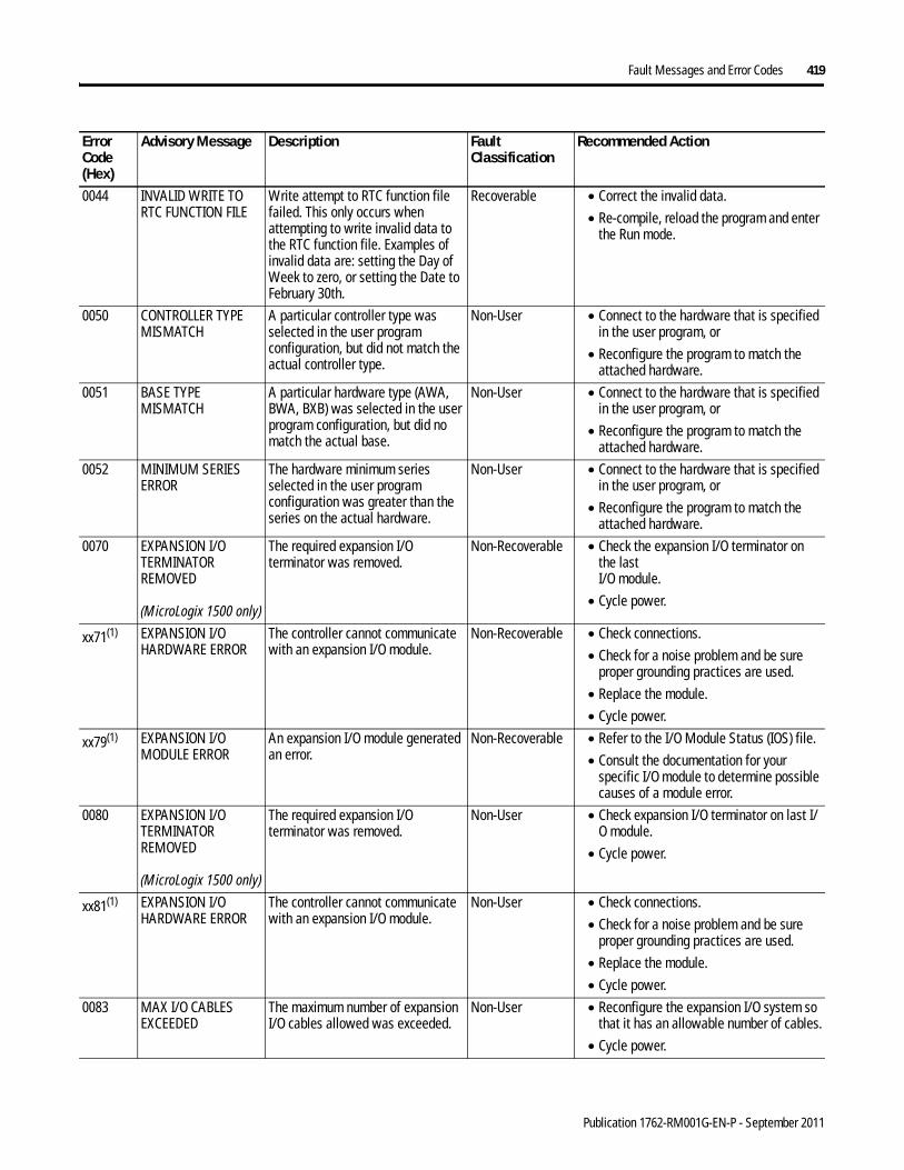
Fault Messages and Error Codes 419
0044 INVALID WRITE TO RTC FUNCTION FILE
Write attempt to RTC function file failed. This only occurs when attempting to write invalid data to the RTC function file. Examples of invalid data are: setting the Day of Week to zero, or setting the Date to February 30th.
Recoverable • Correct the invalid data.
• Re-compile, reload the program and enter the Run mode.
0050 CONTROLLER TYPE MISMATCH
A particular controller type was selected in the user program configuration, but did not match the actual controller type.
Non-User • Connect to the hardware that is specified in the user program, or
• Reconfigure the program to match the attached hardware.
0051 BASE TYPE MISMATCH
A particular hardware type (AWA, BWA, BXB) was selected in the user program configuration, but did no match the actual base.
Non-User • Connect to the hardware that is specified in the user program, or
• Reconfigure the program to match the attached hardware.
0052 MINIMUM SERIES ERROR
The hardware minimum series selected in the user program configuration was greater than the series on the actual hardware.
Non-User • Connect to the hardware that is specified in the user program, or
• Reconfigure the program to match the attached hardware.
0070 EXPANSION I/O TERMINATOR REMOVED
(MicroLogix 1500 only)
The required expansion I/O terminator was removed.
Non-Recoverable • Check the expansion I/O terminator on the last I/O module.
• Cycle power.
xx71(1) EXPANSION I/O HARDWARE ERROR
The controller cannot communicate with an expansion I/O module.
Non-Recoverable • Check connections.
• Check for a noise problem and be sure proper grounding practices are used.
• Replace the module.
• Cycle power.
xx79(1) EXPANSION I/O MODULE ERROR
An expansion I/O module generated an error.
Non-Recoverable • Refer to the I/O Module Status (IOS) file.
• Consult the documentation for your specific I/O module to determine possible causes of a module error.
0080 EXPANSION I/O TERMINATOR REMOVED
(MicroLogix 1500 only)
The required expansion I/O terminator was removed.
Non-User • Check expansion I/O terminator on last I/O module.
• Cycle power.
xx81(1) EXPANSION I/O HARDWARE ERROR
The controller cannot communicate with an expansion I/O module.
Non-User • Check connections.
• Check for a noise problem and be sure proper grounding practices are used.
• Replace the module.
• Cycle power.
0083 MAX I/O CABLES EXCEEDED
The maximum number of expansion I/O cables allowed was exceeded.
Non-User • Reconfigure the expansion I/O system so that it has an allowable number of cables.
• Cycle power.
Error Code (Hex)
Advisory Message Description Fault Classification
Recommended Action
Publication 1762-RM001G-EN-P - September 2011
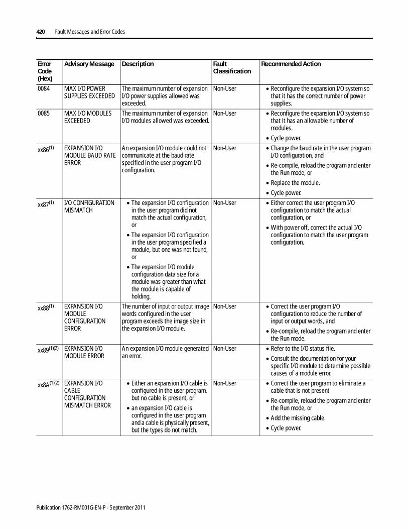
420 Fault Messages and Error Codes
0084 MAX I/O POWER SUPPLIES EXCEEDED
The maximum number of expansion I/O power supplies allowed was exceeded.
Non-User • Reconfigure the expansion I/O system so that it has the correct number of power supplies.
0085 MAX I/O MODULES EXCEEDED
The maximum number of expansion I/O modules allowed was exceeded.
Non-User • Reconfigure the expansion I/O system so that it has an allowable number of modules.
• Cycle power.
xx86(1) EXPANSION I/O MODULE BAUD RATE ERROR
An expansion I/O module could not communicate at the baud rate specified in the user program I/O configuration.
Non-User • Change the baud rate in the user program I/O configuration, and
• Re-compile, reload the program and enter the Run mode, or
• Replace the module.
• Cycle power.
xx87(1) I/O CONFIGURATION MISMATCH
• The expansion I/O configuration in the user program did not match the actual configuration, or
• The expansion I/O configuration in the user program specified a module, but one was not found, or
• The expansion I/O module configuration data size for a module was greater than what the module is capable of holding.
Non-User • Either correct the user program I/O configuration to match the actual configuration, or
• With power off, correct the actual I/O configuration to match the user program configuration.
xx88(1) EXPANSION I/O MODULE CONFIGURATION ERROR
The number of input or output image words configured in the user program exceeds the image size in the expansion I/O module.
Non-User • Correct the user program I/O configuration to reduce the number of input or output words, and
• Re-compile, reload the program and enter the Run mode.
xx89(1)(2) EXPANSION I/O MODULE ERROR
An expansion I/O module generated an error.
Non-User • Refer to the I/O status file.
• Consult the documentation for your specific I/O module to determine possible causes of a module error.
xx8A(1)(2) EXPANSION I/O CABLE CONFIGURATION MISMATCH ERROR
• Either an expansion I/O cable is configured in the user program, but no cable is present, or
• an expansion I/O cable is configured in the user program and a cable is physically present, but the types do not match.
Non-User • Correct the user program to eliminate a cable that is not present
• Re-compile, reload the program and enter the Run mode, or
• Add the missing cable.
• Cycle power.
Error Code (Hex)
Advisory Message Description Fault Classification
Recommended Action
Publication 1762-RM001G-EN-P - September 2011

Fault Messages and Error Codes 421
Contacting Rockwell Automation for Assistance
If you need to contact Rockwell Automation or local distributor for assistance, it is helpful to obtain the following information ready:
• controller type, series letter, and revision letter of the base unit• series letter, revision letter, and firmware (FRN) number of the processor
(on bottom side of processor unit)
• controller LED status• controller error codes (found in S2:6 of status file).
Rockwell Automation phone numbers are listed on the back cover of this manual.
To contact us via the Internet, go to http://www.rockwellautomation.com.
xx8B(1)(2) EXPANSION I/O POWER SUPPLY CONFIGURATION MISMATCH ERROR
• Either an expansion I/O power supply is configured in the user program, but no power supply is present, or
• an expansion I/O power supply is configured in the user program and a power supply is physically present, but the types do not match.
Non-User • Correct the user program to eliminate a power supply that is not present
• Re-compile, reload the program and enter the Run mode, or
• With power removed, add the missing power supply.
xx8C(1)(2) EXPANSION I/O OBJECT TYPE MISMATCH
An expansion I/O object (i.e. cable, power supply, or module) in the user program I/O configuration is not the same object type as is physically present.
Non-User • Correct the user program I/O configuration so that the object types match the actual configuration, and
• Re-compile, reload the program and enter the Run mode. Or
• Correct the actual configuration to match the user program I/O configuration.
• Cycle power.
0x1F39 INVALID STRING LENGTH(3)
The first word of string data contains a negative, zero, or value greater than 82.
Recoverable Check the first word of the string data element for invalid values and correct the data.
(1) xx indicates module number. If xx = 0, problem cannot be traced to a specific module.
(2) The xx in this error code means that the error occurs at the location of the last properly configured Expansion I/O module +1. You should use this information in conjunction with the specific error code to determine the source of the problem.
(3) Applies to MicroLogix 1500 1764-LSP Series B and 1764-LRP Processors.
Error Code (Hex)
Advisory Message Description Fault Classification
Recommended Action
TIP You can also check the FRN by looking at word S:59 (Operating System FRN) in the Status File.
Publication 1762-RM001G-EN-P - September 2011

422 Fault Messages and Error Codes
Notes:
Publication 1762-RM001G-EN-P - September 2011

Appendix E
Protocol Configuration
Use the information in this appendix for configuring communication protocols. The following protocols are supported from any RS-232 communication channel:
• DH-485• DF1 Full-Duplex • DF1 Half-Duplex• DF1 Radio Modem• Modbus™ RTU• ASCII
This appendix is organized into the following sections:
• DH-485 Communication Protocol on page 423• DF1 Full-Duplex Protocol on page 426• DF1 Half-Duplex Protocol on page 427• DF1 Radio Modem Protocol on page 439• Modbus RTU Protocol on page 447• ASCII Driver on page 456
See your controller’s User Manual for information about required network devices and accessories.
DH-485 Communication Protocol
The information in this section describes the DH-485 network functions, network architecture, and performance characteristics. It also helps you plan and operate the controller on a DH-485 network.
DH-485 Network Description
The DH-485 protocol defines the communication between multiple devices that coexist on a single pair of wires. DH-485 protocol uses RS-485 Half-Duplex as its physical interface. (RS-485 is a definition of electrical characteristics; it is not a protocol.) RS-485 uses devices that are capable of co-existing on a common data circuit, thus allowing data to be easily shared between devices.
The DH-485 network offers:
• interconnection of 32 devices• multi-master capability
423 Publication 1762-RM001G-EN-P - September 2011
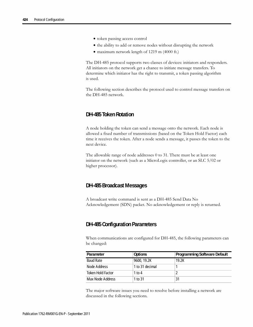
424 Protocol Configuration
• token passing access control• the ability to add or remove nodes without disrupting the network• maximum network length of 1219 m (4000 ft.)
The DH-485 protocol supports two classes of devices: initiators and responders. All initiators on the network get a chance to initiate message transfers. To determine which initiator has the right to transmit, a token passing algorithm is used.
The following section describes the protocol used to control message transfers on the DH-485 network.
DH-485 Token Rotation
A node holding the token can send a message onto the network. Each node is allowed a fixed number of transmissions (based on the Token Hold Factor) each time it receives the token. After a node sends a message, it passes the token to the next device.
The allowable range of node addresses 0 to 31. There must be at least one initiator on the network (such as a MicroLogix controller, or an SLC 5/02 or higher processor).
DH-485 Broadcast Messages
A broadcast write command is sent as a DH-485 Send Data No Acknowledgement (SDN) packet. No acknowledgement or reply is returned.
DH-485 Configuration Parameters
When communications are configured for DH-485, the following parameters can be changed:
The major software issues you need to resolve before installing a network are discussed in the following sections.
Parameter Options Programming Software DefaultBaud Rate 9600, 19.2K 19.2K
Node Address 1 to 31 decimal 1
Token Hold Factor 1 to 4 2
Max Node Address 1 to 31 31
Publication 1762-RM001G-EN-P - September 2011
Protocol Configuration 425
Software Considerations
Software considerations include the configuration of the network and the parameters that can be set to the specific requirements of the network. The following are major configuration factors that have a significant effect on network performance:
• number of nodes on the network• addresses of those nodes• baud rate
The following sections explain network considerations and describe ways to select parameters for optimum network performance (speed). Refer to your programming software’s documentation for more information.
Number of Nodes
The number of nodes on the network directly affects the data transfer time between nodes. Unnecessary nodes (such as a second programming terminal that is not being used) slow the data transfer rate. The maximum number of nodes on the network is 32.
Setting Node Addresses
The best network performance occurs when node addresses are assigned in sequential order. Initiators, such as personal computers, should be assigned the lowest numbered addresses to minimize the time required to initialize the network. The valid range for the MicroLogix controllers is 1 to 31 (controllers cannot be node 0). The default setting is 1. The node address is stored in the controller Communications Status file (CS0:5/0 to CS0:5/7). Configure the node address via Channel Configuration using RSLogix 500. Select the Channel 0 tab. The node address is listed as Source ID.
Setting Controller Baud Rate
The best network performance occurs at the highest baud rate, which is 19200. This is the default baud rate for a MicroLogix devices on the DH-485 network. All devices must be at the same baud rate. This rate is stored in the controller Communications Status file (CS0:5/8 to CS0:5/15). Configure the baud rate via Channel Configuration using RSLogix 500. Select the Channel 0 tab.
Publication 1762-RM001G-EN-P - September 2011

426 Protocol Configuration
Setting Maximum Node Address
Once you have an established network set up, and are confident that you will not be adding more devices, you may enhance performance by adjusting the maximum node address of your controllers. It should be set to the highest node address being used.
MicroLogix 1200 and 1500 Remote Packet Support
These controllers can respond and initiate with device’s communications (or commands) that do not originate on the local DH-485 network. This is useful in installations where communication is needed between the DH-485 and DH+ networks.
DF1 Full-Duplex Protocol
DF1 Full-Duplex protocol provides a point-to-point connection between two devices. DF1 Full-Duplex protocol combines data transparency (American National Standards Institute ANSI - X3.28-1976 specification subcategory D1) and 2-way simultaneous transmission with embedded responses (subcategory F1).
The MicroLogix controllers support the DF1 Full-Duplex protocol via RS-232 connection to external devices, such as computers, or other controllers that support DF1 Full-Duplex.
DF1 is an open protocol. Refer to DF1 Protocol and Command Set Reference Manual, Allen-Bradley publication 1770-6.5.16, for more information.
DF1 Full-Duplex Operation
DF1 Full-Duplex protocol (also referred to as DF1 point-to-point protocol) is useful where RS-232 point-to-point communication is required. This type of protocol supports simultaneous transmissions between two devices in both directions. DF1 protocol controls message flow, detects and signals errors, and retries if errors are detected.
IMPORTANT All devices should be set to the same maximum node address.
Publication 1762-RM001G-EN-P - September 2011

Protocol Configuration 427
When the system driver is DF1 Full-Duplex, the following parameters can be changed:
DF1 Half-Duplex Protocol
With MicroLogix 1200 FRN 7 and MicroLogix 1500 FRN 8, a DF1 Half-Duplex Master driver has been added to complement the DF1 Half-Duplex Slave driver already available in the MicroLogix 1200 and 1500 controllers.
DF1 Half-Duplex Protocol
DF1 Half-Duplex protocol provides a multi-drop single master/multiple slave network. In contrast to the DF1 Full-Duplex protocol, communication takes place in one direction at a time. You can use the RS-232 port on the MicroLogix controller as both a Half-Duplex programming port, and a Half-Duplex peer-to-peer messaging port.
MicroLogix 1200 and 1500 controllers support Half-Duplex modems using RTS/CTS hardware handshaking.
DF1 Full-Duplex Configuration Parameters(All MicroLogix 1200 and MicroLogix 1500 Controllers)Parameter Options Programming Software
DefaultChannel MicroLogix 1200 and MicroLogix 1500 1764-LSP: Channel 0
MicroLogix 1500 1764-LRP: Channel 0 or 1
0 (1200 & LSP)
0 or 1 (LRP)Driver DF1 Full Duplex DF1 Full DuplexBaud Rate 300, 600, 1200, 2400, 4800, 9600, 19.2K, 38.4K 19.2KParity none, even noneSource ID (Node Address) 0 to 254 decimal 1Control Line no handshaking, Full-Duplex modem no handshakingError Detection CRC, BCC CRCEmbedded Responses auto detect, enabled auto detectDuplicate Packet (Message) Detect enabled, disabled enabledACK Timeout (x20 ms) 1 to 65535 counts (20 ms increments) 50 countsNAK retries 0 to 255 3 retriesENQ retries 0 to 255 3 retriesStop Bits not a setting, always 1 1
TIP DF1 Half-Duplex Master driver can be used with the following controllers:
MicroLogix 1200, FRN 7 and higher
MicroLogix 1500, 1764-LSP, FRN 8 and higher
MicroLogix 1500, 1764-LRP, FRN 8 and higher (Channel 1 only)
Publication 1762-RM001G-EN-P - September 2011

428 Protocol Configuration
DF1 Half-Duplex supports up to 255 devices (addresses 0 to 254, with address 255 reserved for master broadcasts). Note: When configuring a message instruction, set the target node address to -1 for broadcast messages.
Broadcast messages are handled as follows:
DF1 Half-Duplex Master Driver Broadcast Messages
A broadcast write command initiated by the DF1 half-duplex master is received and executed by all DF1 half-duplex slaves. A broadcast write command received by the DF1 half-duplex master after polling a DF1 half-duplex slave is received, acknowledged and re-broadcast without being executed by the DF1 half-duplex master. It is treated like any other slave-to-slave command, except that no acknowledgement is expected after re-broadcast.
DF1 Half-Duplex Slave Driver Broadcast Messages
When a broadcast write command is initiated by a DF1 half-duplex slave, it is queued up just like any other MSG command until it receives a poll from the DF1 half-duplex master. After transmitting the broadcast write command, the DF1 half-duplex slave receives an acknowledgement that the DF1 half-duplex master received the packet without error. When the DF1 half-duplex master re-broadcasts the broadcast write command, the initiating DF1 half-duplex slave receives and executes the command along with all of the other slave nodes receiving the broadcast packet. No acknowledgement or reply is returned.
Choosing a Polling Mode for DF1 Half-Duplex Master
A master station can be configured to communicate with slave stations in either Message-based polling mode or Standard polling mode. The pros and cons of each polling mode are described below.
Message-Based Polling Mode
Message-based polling mode is best used in networks when communication with the slave stations is not time critical and where the user needs to be able to limit when and how often the master station communicates with each slave station. It is not recommended for larger systems that require time critical communication between the master and all the slave stations, or for systems where slave station-initiated messages are going to be used.
Publication 1762-RM001G-EN-P - September 2011

Protocol Configuration 429
With Message-Based polling mode, the only time a master station communicates with a slave station is when a message (MSG) instruction in ladder logic is triggered to that particular slave station’s address. This polling mode gives the user complete control (through ladder logic) over when and how often to communicate with each slave station.
If multiple MSG instructions are triggered “simultaneously,” they will be executed in order, one at a time, to completion (i.e., the first MSG queued up will be transmitted and completed to done or error before the next queued up MSG is transmitted). Any time a message is triggered to a slave station that cannot respond (for instance, if its modem fails), the message will go through retries and time-outs that will slow down the execution of all the other queued up messages. The minimum time to message to every responding slave station increases linearly with the number of slave stations that cannot respond.
If the Message-based selection is “allow slaves to initiate messages,” a slave station can initiate a message to the master station (polled report by exception messaging) or to another slave station (slave-to-slave messaging). The MSG command packet will remain in that slave station’s transmit queue until the master station triggers its own MSG command packet to it (which could be seconds, minutes or hours later, depending on the master’s ladder logic).
If the Message-based selection is “don’t allow slaves to initiate messages,” then even if a slave station triggers and queues up a MSG instruction in its ladder logic, the master station will not process it.
Standard Polling Mode
Standard polling mode is strongly recommended for larger systems that require time critical communication between the master and all the slave stations, or for any system where slave station-initiated messages are going to be used (this includes slave programming over the network, since this uses the same mechanism that slave-to-slave messaging uses). The Active Node Table “automatically” keeps track of which slaves are (and are not) communicating. Standard polling mode should not be used in cases where the user needs to be able to limit when and how often the master station communicates with each slave station.
Standard polling mode causes the master station to continuously send one or more 4-byte poll packets to each slave station address configured by the user in the poll list(s) in round robin fashion – as soon as the end of the polling list is reached, the master station immediately goes back and starts polling slave stations from the top of the polling list over again. This is independent and asynchronous to any MSG instructions that might be triggered in the master station ladder logic. In fact, this polling continues even while the master station is in program mode!
When a MSG instruction is triggered while the master station is in run mode, the master station will transmit the message packet just after it finishes polling the current slave station in the poll list and before it starts polling the next slave station in the poll list (no matter where it currently is in the poll list). If multiple MSG
Publication 1762-RM001G-EN-P - September 2011

430 Protocol Configuration
instructions have been triggered “simultaneously,” at least four message packets may be sent out between two slave station polls. Each of these messages will have an opportunity to complete when the master polls the slave station that was addressed in the message packet as it comes to it in the poll list.
If each of the transmitted message packets is addressed to a different slave station, the order of completion will be based upon which slave station address comes up next in the poll list, not the order in which the MSG instructions were executed and transmitted.
When a slave station receives a poll packet from the master station, if it has one or more message packets queued up to transmit (either replies to a command received earlier or MSG commands triggered locally in ladder logic), the slave station will transmit the first message packet in the transmit queue.
If the standard mode selection is “single message per poll scan,” then the master station will then go to the next station in the poll list. If the standard mode selection is “multiple messages per poll scan,” the master station will continue to poll this slave station until its transmit queue is empty.
The master station “knows” the slave station has no message packets queued up to transmit when the slave station responds to the master poll packet with a 2-byte poll response.
Every time a slave station responds or fails to respond to its poll packet, the master station “automatically” updates its Active Node Table (again, even if it’s in program mode). In this list, one bit is assigned to each possible slave station address (0 to 254). If a slave station does not respond when it is polled, its Active Node Table bit is cleared. If it does respond when it is polled, its Active Node Table bit is set. Besides being an excellent online troubleshooting tool, two common uses of the Active Node Table are to report good/bad communication status for all slave stations to an operator interface connected to the master station for monitoring, alarming and logging purposes, and to precondition MSG instructions to each particular slave.
This second use is based on the supposition that if a slave station did not respond the last time it was polled, it may not be able to receive and respond to a MSG instruction now, and so it would most likely process the maximum number of retries and time-outs before completing in error. This slows down both the poll scan and any other messaging going on. Using this technique, the minimum time to message to every responding slave station actually decreases as the number of slave stations that can’t respond increases.
IMPORTANT In order to remotely monitor and program the slave stations over the half-duplex network while the master station is configured for Standard polling mode, the programming computer DF1 slave driver (typically Rockwell Software RSLinx™) station address must be included in the master station poll list.
Publication 1762-RM001G-EN-P - September 2011

Protocol Configuration 431
About Polled Report-by-Exception
Polled report-by-exception lets a slave station initiate data transfer to its master station, freeing the master station from having to constantly read blocks of data from each slave station to determine if any slave input or data changes have occurred. Instead, through user programming, the slave station monitors its own inputs for a change of state or data, which triggers a block of data to be written to the master station when the master station polls the slave.
About Slave-to-Slave Messaging
If one slave station has a message to send to another, it simply includes the destination slave station’s address in the message instruction’s destination field in place of the master station’s address when responding to a poll. The master station checks the destination station address in every packet header it receives from any slave station. If the address does not match the slave’s own station address, the entire message is forwarded back onto the telemetry network to the appropriate slave station, without any further processing.
Addressing Tips
Each station on the network, including the master station, must have a unique address. The address range is 0 to 254, so you can have a maximum of 255 stations on a single telemetry network. Station address 255 is the broadcast address, which you cannot select as a station’s individual address.
DF1 Half-Duplex Master Standard Polling Mode
With standard polling mode, the master device initiates all communication by polling each slave address configured in the priority and normal polling ranges. The slave device may only transmit message packets when it is polled by the master. Based on a slave’s inclusion in the priority and/or normal poll ranges, the master polls each slave on a regular and sequential basis to allow slave devices an opportunity to communicate. During a polling sequence, the master polls a slave either repeatedly until the slave indicates that it has no more message packets to transmit (“standard polling mode, multiple messages per scan”) or just one time per polling sequence (“standard polling mode, single message per scan”), depending on how the master is configured.
The polling algorithm polls all of the priority slave addresses each poll scan (priority low to priority high) and a subset of the normal slave address range. The number of normal slave addresses to poll each poll scan is determined by the Normal Poll Group Size configuration parameter. In order to poll all of the slave addresses each poll scan with equal priority, you may define the entire slave address
Publication 1762-RM001G-EN-P - September 2011
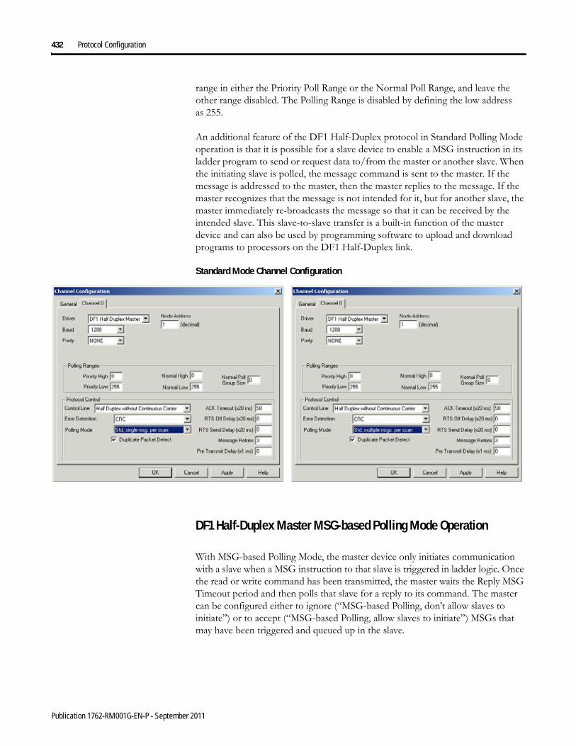
432 Protocol Configuration
range in either the Priority Poll Range or the Normal Poll Range, and leave the other range disabled. The Polling Range is disabled by defining the low address as 255.
An additional feature of the DF1 Half-Duplex protocol in Standard Polling Mode operation is that it is possible for a slave device to enable a MSG instruction in its ladder program to send or request data to/from the master or another slave. When the initiating slave is polled, the message command is sent to the master. If the message is addressed to the master, then the master replies to the message. If the master recognizes that the message is not intended for it, but for another slave, the master immediately re-broadcasts the message so that it can be received by the intended slave. This slave-to-slave transfer is a built-in function of the master device and can also be used by programming software to upload and download programs to processors on the DF1 Half-Duplex link.
Standard Mode Channel Configuration
DF1 Half-Duplex Master MSG-based Polling Mode Operation
With MSG-based Polling Mode, the master device only initiates communication with a slave when a MSG instruction to that slave is triggered in ladder logic. Once the read or write command has been transmitted, the master waits the Reply MSG Timeout period and then polls that slave for a reply to its command. The master can be configured either to ignore (“MSG-based Polling, don’t allow slaves to initiate”) or to accept (“MSG-based Polling, allow slaves to initiate”) MSGs that may have been triggered and queued up in the slave.
Publication 1762-RM001G-EN-P - September 2011

Protocol Configuration 433
Message-Based Polling Mode Channel Configuration
When the system driver is DF1 Half-Duplex Master, the following parameters can be changed:
DF1 Half-Duplex Master Configuration Parameters(MicroLogix 1200, FRN 7 and higherMicroLogix 1500, 1764-LSP, FRN 8 and higherMicroLogix 1500, 1764-LRP, FRN 8 and higher [Channel 1 only])
Parameter Options Programming Software Default
Channel MicroLogix 1200 and MicroLogix 1500 1764-LSP: Channel 0
MicroLogix 1500 1764-LRP: Channel 1 only
0 (1200 & LSP)
1 (LRP)
Driver DF1 Half Duplex Master
Baud Rate 300, 600, 1200, 2400, 4800, 9600, 19.2K, 38.4K 19.2K
Parity none, even none
Node Address 0 to 254 decimal (255 is reserved for broadcast) 1
Control Line No Handshaking, Half-Duplex Modem (RTS/CTS Handshaking), Full-Duplex Modem (RTS on) No Handshaking
Error Detection CRC, BCC CRC
Duplicate Packet Detect
enabled, disabled
Detects and eliminates duplicate responses to a message. Duplicate packets may be sent under noisy communication conditions if the sender’s Message Retries are set greater than 0.
enabled
RTS Off Delay (x20 ms)
0 to 65535 (can be set in 20 ms increments) – only with control line set to “Half Duplex Modem (RTS/CTS Handshaking)”
Specifies the delay time between when the last serial character is sent to the modem and when RTS is deactivated. Gives the modem extra time to transmit the last character of a packet.
0
Publication 1762-RM001G-EN-P - September 2011

434 Protocol Configuration
RTS Send Delay (x20 ms)
0 to 65535 (can be set in 20 ms increments) – only with control line set to “Half Duplex Modem (RTS/CTS Handshaking)”
Specifies the time delay between setting RTS until checking for the CTS response. For use with modems that are not ready to respond with CTS immediately upon receipt of RTS.
0
Message Retries 0 to 255
Specifies the number of times the master device attempts to re-send a message packet when it does not receive an ACK from the slave device. For use in noisy environments where acknowledgements may become corrupted in transmission.
3
Pre Transmit Delay (x1 ms)
0 to 65535 (can be set in 1 ms increments)
When the Control Line is set to “No Handshaking”, this is the delay time before transmission. Required for 1761-NET-AIC physical Half-Duplex networks. The 1761-NET-AIC needs 2 ms of delay time to change from transmit to receive mode.
When the Control Line is set to “Half-Duplex Modem (RTS/CTS Handshaking)”, this is the minimum time delay between receiving the last character of a packet and the next RTS assertion.
0
ACK Timeout (x20 ms)
0 to 255 (can be set in 20 ms increments)
Specifies the amount of time the master will wait for an acknowledgement to a message it has transmitted before it retries the message or errors out the message instruction.
This timeout value is also used for the poll response timeout.
50
Reply MSG Timeout (x 20 ms)
0 to 255 (can be set in 20 ms increments) – only with MSG-based Polling Modes
Specifies the amount of time the master will wait after receiving an ACK to a master-initiated MSG before polling the slave station for its reply.
1
Priority Polling Range – High
Select the last slave station address to priority poll – only with Standard Polling Modes. 0
Priority Polling Range – Low
Select the first slave station address to priority poll. Entering 255 disables priority polling – only with Standard Polling Modes.
255
Normal Polling Range – High
Select the last slave station address to normal poll – only with Standard Polling Modes. 0
Normal Polling Range – Low
Select the first slave station address to normal poll. Entering 255 disables normal polling – only with Standard Polling Modes.
255
Normal Poll Group Size
Enter the quantity of active stations located in the normal poll range that you want polled during a scan through the normal poll range before returning to the priority poll range. If no stations are configured in the Priority Polling Range, leave this parameter at 0.
0
DF1 Half-Duplex Master Configuration Parameters(MicroLogix 1200, FRN 7 and higherMicroLogix 1500, 1764-LSP, FRN 8 and higherMicroLogix 1500, 1764-LRP, FRN 8 and higher [Channel 1 only])
Parameter Options Programming Software Default
Publication 1762-RM001G-EN-P - September 2011
Protocol Configuration 435
RTS Send Delay (x20 ms)
0 to 65535 (can be set in 20 ms increments) – only with control line set to “Half Duplex Modem (RTS/CTS Handshaking)”
Specifies the time delay between setting RTS until checking for the CTS response. For use with modems that are not ready to respond with CTS immediately upon receipt of RTS.
0
Message Retries 0 to 255
Specifies the number of times the master device attempts to re-send a message packet when it does not receive an ACK from the slave device. For use in noisy environments where acknowledgements may become corrupted in transmission.
3
Pre Transmit Delay (x1 ms)
0 to 65535 (can be set in 1 ms increments)
When the Control Line is set to “No Handshaking”, this is the delay time before transmission. Required for 1761-NET-AIC physical Half-Duplex networks. The 1761-NET-AIC needs 2 ms of delay time to change from transmit to receive mode.
When the Control Line is set to “Half-Duplex Modem (RTS/CTS Handshaking)”, this is the minimum time delay between receiving the last character of a packet and the next RTS assertion.
0
ACK Timeout (x20 ms)
0 to 255 (can be set in 20 ms increments)
Specifies the amount of time the master will wait for an acknowledgement to a message it has transmitted before it retries the message or errors out the message instruction.
This timeout value is also used for the poll response timeout.
50
Reply MSG Timeout (x 20 ms)
0 to 255 (can be set in 20 ms increments) – only with MSG-based Polling Modes
Specifies the amount of time the master will wait after receiving an ACK to a master-initiated MSG before polling the slave station for its reply.
1
Priority Polling Range – High
Select the last slave station address to priority poll – only with Standard Polling Modes. 0
Priority Polling Range – Low
Select the first slave station address to priority poll. Entering 255 disables priority polling – only with Standard Polling Modes.
255
Normal Polling Range – High
Select the last slave station address to normal poll – only with Standard Polling Modes. 0
Normal Polling Range – Low
Select the first slave station address to normal poll. Entering 255 disables normal polling – only with Standard Polling Modes.
255
Normal Poll Group Size
Enter the quantity of active stations located in the normal poll range that you want polled during a scan through the normal poll range before returning to the priority poll range. If no stations are configured in the Priority Polling Range, leave this parameter at 0.
0
DF1 Half-Duplex Master Configuration Parameters(MicroLogix 1200, FRN 7 and higherMicroLogix 1500, 1764-LSP, FRN 8 and higherMicroLogix 1500, 1764-LRP, FRN 8 and higher [Channel 1 only])
Parameter Options Programming Software Default
Publication 1762-RM001G-EN-P - September 2011
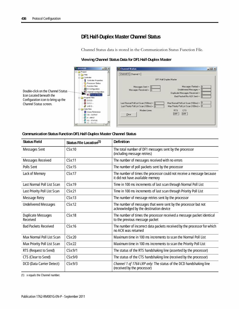
436 Protocol Configuration
DF1 Half-Duplex Master Channel Status
Channel Status data is stored in the Communication Status Function File.
Viewing Channel Status Data for DF1 Half-Duplex Master
Communication Status Function DF1 Half-Duplex Master Channel Status
Status Field Status File Location(1) Definition
Messages Sent CSx:10 The total number of DF1 messages sent by the processor (including message retries)
Messages Received CSx:11 The number of messages received with no errors
Polls Sent CSx:15 The number of poll packets sent by the processor
Lack of Memory CSx:17 The number of times the processor could not receive a message because it did not have available memory
Last Normal Poll List Scan CSx:19 Time in 100 ms increments of last scan through Normal Poll List
Last Priority Poll List Scan CSx:21 Time in 100 ms increments of last scan through Priority Poll List
Message Retry CSx:13 The number of message retries sent by the processor
Undelivered Messages CSx:12 The number of messages that were sent by the processor but not acknowledged by the destination device
Duplicate Messages Received
CSx:18 The number of times the processor received a message packet identical to the previous message packet
Bad Packets Received CSx:16 The number of incorrect data packets received by the processor for which no ACK was returned
Max Normal Poll List Scan CSx:20 Maximum time in 100 ms increments to scan the Normal Poll List
Max Priority Poll List Scan CSx:22 Maximum time in 100 ms increments to scan the Priority Poll List
RTS (Request to Send) CSx:9/1 The status of the RTS handshaking line (asserted by the processor)
CTS (Clear to Send) CSx:9/0 The status of the CTS handshaking line (received by the processor)
DCD (Data Carrier Detect) CSx:9/3 Channel 1 of 1764-LRP only: The status of the DCD handshaking line (received by the processor)
(1) x equals the Channel number.
Double-click on the Channel Status Icon Located beneath the Configuration icon to bring up the Channel Status screen.
Publication 1762-RM001G-EN-P - September 2011

Protocol Configuration 437
Monitor Active Stations
To see which slave stations are active when the channel is configured for Standard Polling Mode (either single or multiple message per scan), view the DF1 Half-Duplex Master Active Node Table. The table is stored in the Communications Status Function File, words CSx:27 to CSx:42, where x is the channel number (x = 0 for MicroLogix 1200 and MicroLogix 1500 1764-LSP; x = 1 for MicroLogix 1500 1764-LRP). Each bit in the table represents a station on the link, from 0 to 254, starting with CSx:27/0 for address 0 and CSx:42/14 for address 254. The bit for address 255 (CSx:42/15) is never set, since it is the broadcast address, which never gets polled.
When valid Normal and/or Priority Poll Ranges are defined:
• if a slave responded the last time it was polled by the master, the bit corresponding to its address is set (1 = active).
• if a slave didn’t respond the last time it was polled by the master, the bit corresponding to its address is cleared (0 = inactive).
If you are using RSLogix 500 version 6.10.10 or higher, you can view the active node table by clicking on “Processor Status” and then selecting the tab for the DF1 Master channel.
Example Active Node Table
At power-up or after reconfiguration, the master station assumes that all slave stations are inactive. A station is shown active only after it responds to a poll packet.
TIP The bit corresponding to the address configured for the DF1 Master is always cleared because the master address never gets polled.
Publication 1762-RM001G-EN-P - September 2011

438 Protocol Configuration
DF1 Half-Duplex Slave Configuration
When the system driver is DF1 Half-Duplex Slave, the following parameters can be changed:
DF1 Half-Duplex Slave Configuration Parameters(All MicroLogix 1200 and MicroLogix 1500 Controllers)
Parameter Options Programming Software Default
Channel MicroLogix 1200 and MicroLogix 1500 1764-LSP: Channel 0
MicroLogix 1500 1764-LRP: Channel 0 or 1
0 (1200 & LSP)
0 or 1 (LRP)
Driver DF1 Half Duplex Slave
Baud Rate 300, 600, 1200, 2400, 4800, 9600, 19.2K, 38.4K 19.2K
Parity none, even none
Node Address 0 to 254 decimal (255 is reserved for broadcast) 1
Control Line No Handshaking, Half-Duplex Modem No Handshaking
Error Detection CRC, BCC CRC
EOT Suppression enabled, disabled
When EOT Suppression is enabled, the slave does not respond when polled if no message is queued. This saves modem transmission power when there is no message to transmit.
disabled
Duplicate Packet (Message) Detect
enabled, disabled
Detects and eliminates duplicate responses to a message. Duplicate packets may be sent under noisy communication conditions if the sender’s Message Retries are set greater than 0.
enabled
Poll Timeout(x20 ms)
0 to 65535 (can be set in 20 ms increments)
Poll timeout only applies when a slave device initiates a MSG instruction. It is the amount of time that the slave device waits for a poll from the master device. If the slave device does not receive a poll within the Poll Timeout, a MSG instruction error is generated, and the ladder program needs to re-queue the MSG instruction. If you are using a MSG instruction, it is recommended that a Poll Timeout value of zero is not used. Poll Timeout is disabled when set to zero.
3000
RTS Off Delay (x20 ms)
0 to 65535 (can be set in 20 ms increments) – only with control line set to “Half Duplex Modem (RTS/CTS Handshaking)”
Specifies the delay time between when the last serial character is sent to the modem and when RTS is deactivated. Gives the modem extra time to transmit the last character of a packet.
0
RTS Send Delay (x20 ms)
0 to 65535 (can be set in 20 ms increments) – only with control line set to “Half Duplex Modem (RTS/CTS Handshaking)”
Specifies the time delay between setting RTS until checking for the CTS response. For use with modems that are not ready to respond with CTS immediately upon receipt of RTS.
0
Publication 1762-RM001G-EN-P - September 2011
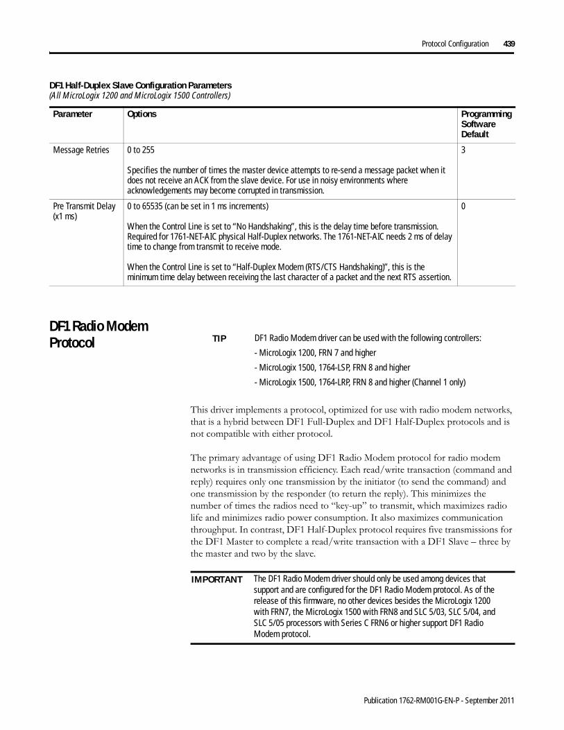
Protocol Configuration 439
DF1 Radio Modem Protocol
This driver implements a protocol, optimized for use with radio modem networks, that is a hybrid between DF1 Full-Duplex and DF1 Half-Duplex protocols and is not compatible with either protocol.
The primary advantage of using DF1 Radio Modem protocol for radio modem networks is in transmission efficiency. Each read/write transaction (command and reply) requires only one transmission by the initiator (to send the command) and one transmission by the responder (to return the reply). This minimizes the number of times the radios need to “key-up” to transmit, which maximizes radio life and minimizes radio power consumption. It also maximizes communication throughput. In contrast, DF1 Half-Duplex protocol requires five transmissions for the DF1 Master to complete a read/write transaction with a DF1 Slave – three by the master and two by the slave.
Message Retries 0 to 255
Specifies the number of times the master device attempts to re-send a message packet when it does not receive an ACK from the slave device. For use in noisy environments where acknowledgements may become corrupted in transmission.
3
Pre Transmit Delay (x1 ms)
0 to 65535 (can be set in 1 ms increments)
When the Control Line is set to “No Handshaking”, this is the delay time before transmission. Required for 1761-NET-AIC physical Half-Duplex networks. The 1761-NET-AIC needs 2 ms of delay time to change from transmit to receive mode.
When the Control Line is set to “Half-Duplex Modem (RTS/CTS Handshaking)”, this is the minimum time delay between receiving the last character of a packet and the next RTS assertion.
0
DF1 Half-Duplex Slave Configuration Parameters(All MicroLogix 1200 and MicroLogix 1500 Controllers)
Parameter Options Programming Software Default
TIP DF1 Radio Modem driver can be used with the following controllers:
- MicroLogix 1200, FRN 7 and higher
- MicroLogix 1500, 1764-LSP, FRN 8 and higher
- MicroLogix 1500, 1764-LRP, FRN 8 and higher (Channel 1 only)
IMPORTANT The DF1 Radio Modem driver should only be used among devices that support and are configured for the DF1 Radio Modem protocol. As of the release of this firmware, no other devices besides the MicroLogix 1200 with FRN7, the MicroLogix 1500 with FRN8 and SLC 5/03, SLC 5/04, and SLC 5/05 processors with Series C FRN6 or higher support DF1 Radio Modem protocol.
Publication 1762-RM001G-EN-P - September 2011

440 Protocol Configuration
Like DF1 Full-Duplex protocol, DF1 Radio Modem allows any node to initiate to any other node at any time (if the radio modem network supports full-duplex data port buffering and radio transmission collision avoidance). Like DF1 Half-Duplex protocol, up to 255 devices are supported, with unique addresses from 0 to 254. A node ignores any packets received that have a destination address other than its own, with the exception of broadcast packets. A broadcast write command initiated by any DF1 radio modem node is executed by all of the other DF1 radio modem nodes that receive it. No acknowledgement or reply is returned.
Unlike either DF1 Full-Duplex or DF1 Half-Duplex protocols, DF1 Radio Modem protocol does not include ACKs, NAKs, ENQs, or poll packets. Data integrity is ensured by the CRC checksum.
Using the DF1 Radio Modem
Using RSLogix 500 version 6.10.10 or higher, the DF1 Radio Modem driver can be configured as the system mode driver for Channel 0 in MicroLogix 1200 (FRN 7 or higher) and MicroLogix 1500 1764-LSP (FRN 8 or higher) and for Channel 1 in MicroLogix 1500 1764-LRP (FRN 8 or higher).
Channel configuration appears as follows. Figure shows Channel 0 configuration, and Figure shows Channel 1 configuration options.
DF1 Radio Modem Channel 0 Configuration (MicroLogix 1200 and MicroLogix 1500, 1764-LSP
Publication 1762-RM001G-EN-P - September 2011
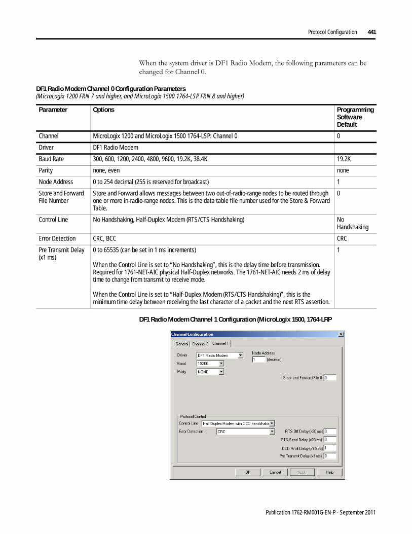
Protocol Configuration 441
When the system driver is DF1 Radio Modem, the following parameters can be changed for Channel 0.
DF1 Radio Modem Channel 1 Configuration (MicroLogix 1500, 1764-LRP
DF1 Radio Modem Channel 0 Configuration Parameters(MicroLogix 1200 FRN 7 and higher, and MicroLogix 1500 1764-LSP FRN 8 and higher)
Parameter Options Programming Software Default
Channel MicroLogix 1200 and MicroLogix 1500 1764-LSP: Channel 0 0
Driver DF1 Radio Modem
Baud Rate 300, 600, 1200, 2400, 4800, 9600, 19.2K, 38.4K 19.2K
Parity none, even none
Node Address 0 to 254 decimal (255 is reserved for broadcast) 1
Store and Forward File Number
Store and Forward allows messages between two out-of-radio-range nodes to be routed through one or more in-radio-range nodes. This is the data table file number used for the Store & Forward Table.
0
Control Line No Handshaking, Half-Duplex Modem (RTS/CTS Handshaking) No Handshaking
Error Detection CRC, BCC CRC
Pre Transmit Delay (x1 ms)
0 to 65535 (can be set in 1 ms increments)
When the Control Line is set to “No Handshaking”, this is the delay time before transmission. Required for 1761-NET-AIC physical Half-Duplex networks. The 1761-NET-AIC needs 2 ms of delay time to change from transmit to receive mode.
When the Control Line is set to “Half-Duplex Modem (RTS/CTS Handshaking)”, this is the minimum time delay between receiving the last character of a packet and the next RTS assertion.
1
Publication 1762-RM001G-EN-P - September 2011

442 Protocol Configuration
When the system driver is DF1 Radio Modem, the following parameters can be changed for Channel 1.
With RSLogix 500 version 6.10.10 and higher, the MicroLogix 1500 1764-LRP offers a “Half-Duplex Modem with DCD Handshaking” Control Line selection. This allows messaging to occur in a Report-by-Exception mode with radio modems using hardware handshaking, based on the status of the DCD. Transmission can only occur when DCD is low, indicating that no other nodes are currently transmitting. Received characters are considered valid while DCD is high.
DF1 Radio Modem Channel 1 Configuration Parameters(MicroLogix 1500 1764-LRP FRN 8 and higher)
Parameter Options Programming Software Default
Channel MicroLogix 1500 1764-LRP: Channel 1 only 1
Driver DF1 Radio Modem
Baud Rate 300, 600, 1200, 2400, 4800, 9600, 19.2K, 38.4K 19.2K
Parity none, even none
Node Address 0 to 254 decimal (255 is reserved for broadcast) 1
Store and Forward File Number
Store and Forward allows messages between two out-of-radio-range nodes to be routed through one or more in-radio-range nodes. This is the starting address for the Store & Forward Table.
0
Control Line No Handshaking, Half Duplex Modem (RTS/CTS) Handshaking, Half Duplex Modem with DCD Handshaking
No Handshaking
Error Detection CRC, BCC CRC
RTS Off Delay (x20 ms)
0 to 65535 (can be set in 20 ms increments) – only with control line set to “Half Duplex Modem (RTS/CTS Handshaking)”
Specifies the delay time between when the last serial character is sent to the modem and when RTS is deactivated. Gives the modem extra time to transmit the last character of a packet.
0
RTS Send Delay (x20 ms)
0 to 65535 (can be set in 20 ms increments) – only with control line set to “Half Duplex Modem (RTS/CTS Handshaking)”
Specifies the time delay between setting RTS until checking for the CTS response. For use with modems that are not ready to respond with CTS immediately upon receipt of RTS.
0
DCD Wait Delay 0 to 255
Specifies the number of times the master device attempts to re-send a message packet when it does not receive an ACK from the slave device. For use in noisy environments where acknowledgements may become corrupted in transmission.
1
Pre Transmit Delay (x1 ms)
0 to 65535 (can be set in 1 ms increments)
When the Control Line is set to “No Handshaking”, this is the delay time before transmission. Required for 1761-NET-AIC physical Half-Duplex networks. The 1761-NET-AIC needs 2 ms of delay time to change from transmit to receive mode.
When the Control Line is set to “Half-Duplex Modem (RTS/CTS Handshaking)”, this is the minimum time delay between receiving the last character of a packet and the next RTS assertion.
0
Publication 1762-RM001G-EN-P - September 2011

Protocol Configuration 443
A DCD Wait Timeout parameter configures the length of time, after triggering a MSG, that the DCD must go low in order for a message to be transmitted. Otherwise, the MSG will error out with a 09 error code.
The DF1 Radio Modem driver can be used in a “pseudo” Master/Slave mode with any radio modems, as long as the designated “Master” node is the only node initiating MSG instructions, and as long as only one MSG instruction is triggered at a time.
For modern serial radio modems that support full-duplex data port buffering and radio transmission collision avoidance, the DF1 Radio Modem driver can be used to set up a “Masterless” peer-to-peer radio network, where any node can initiate communications to any other node at any time, as long as all of the nodes are within radio range so that they receive each other’s transmissions.
Using Store & Forward Capability
DF1 Radio Modem also supports Store & Forward capability in order to forward packets between nodes that are outside of radio range of each other. Each node that is enabled for Store & Forward has a user-configured Store & Forward Table to indicate which received packets it should re-broadcast, based on the packet’s source and destination addresses.
Configuring the Store & Forward Table
The Store & Forward Table can be configured to use any valid binary data table file (B3, B9 through B255) of length 16 words. Each bit in the file corresponds to a DF1 Radio Modem node address. In order to configure a MicroLogix to Store & Forward message packets between two other nodes, the bits corresponding to the addresses of those two other nodes must be set. For instance, if node 2 is used to Store & Forward message packets between nodes 1 and 3, then both bits Bx/1 and
IMPORTANT RSLogix 500 version 6.10.10 allows you to configure the MicroLogix DF1 Radio Modem driver, but does not allow you to configure the Store & Forward Table file. In order to use the Store & Forward capability with RSLogix version 6.10.10, you must download a pre-configured default ladder file for your particular processor from the MicroLogix web site (www.ab.com/micrologix), which has a binary file (B3:0-15) pre-configured for the DF1 Radio Modem Store & Forward Table file.
Publication 1762-RM001G-EN-P - September 2011

444 Protocol Configuration
Bx/3 (where x is the configured data table file number) would have to be set in the Store & Forward Table file (see Figure ). You can set bit 255 to enable Store & Forward of broadcast packets, as well.
Applying DF1 Radio Modem Protocol
If you are using RSLogix 500 version 6.10.10 or higher, you can view the store & forward table by clicking on “Processor Status” and then selecting the tab for the DF1 Master channel.
IMPORTANT Once Store & Forward is enabled, duplicate packet detection is also automatically enabled. Whenever Store & Forward is used within a radio modem network, every node should have a Store & Forward Table file configured, even if all of the bits in the file are cleared, so that duplicate packets will be ignored.
Node 4
No Bits
Node 3
1, 2, 4
Node 2
1, 3, 4
Node 1
No BitsCMD 1
(DST = 4, SRC = 1)REPLY 1
(DST = 1, SRC = 4)
CMD1(1st Rebroadcast)
Note 1
(2nd Rebroadcast)REPLY 1
CMD 1(2nd Rebroadcast)
(1st Rebroadcast)REPLY 1
Note 4
Note 2
Note 1 – The link layer of Node 1 blocks the re-transmission of a packet that is received with the SRC byte equal to the receiving node’s station address. Packets received that originate from the receiving node should never be re-transmitted.
Note 2 – To prevent Node 2 from re-transmitting a duplicate packet, the link layer of Node 2 updates the duplicate packet table with the last 20 packets received.
Note 3 – The link layer of Node 4 blocks the re-transmission of a packet that is received with the SRC byte equal to the receiving node’s station address. Packets received that originate from the receiving node should never be re-transmitted.
Note 4 – To prevent Node 3 from re-transmitting a duplicate packet, the link layer of Node 3 updates the duplicate packet table with the last 20 packets received.
Note 3
Publication 1762-RM001G-EN-P - September 2011

Protocol Configuration 445
Example Store & Forward Table
DF1 Radio Modem Channel Status
Channel Status data is stored in the Communication Status Function File.
Viewing Channel Status for DF1 Radio Modem
Communication Status Function DF1 Radio Modem Channel Status
Status Field Diagnostic File Location(1) Definition
Messages Sent CSx:10 The total number of DF1 messages sent by the processor (including message retries)
Messages Received CSx:11 The number of messages received with no errors
Lack of Memory CSx:17 The number of times the processor could not receive a message because it did not have available memory
Undelivered Messages CSx:12 The number of messages that could not be sent by the processor due to bad modem handshake signals
Double-click on the Channel Status Icon Located beneath the Configuration icon to bring up the Channel Status screen.
Publication 1762-RM001G-EN-P - September 2011

446 Protocol Configuration
DF1 Radio Modem System Limitations
The following questions need to be answered in order to determine if you can implement the new DF1 Radio Modem driver in your radio modem network:
1. Are all of the devices MicroLogix 1200 or 1500 controllers, or SLC 5/03, 5/04 or 5/05 processors?
In order to be configured with the DF1 Radio Modem driver, using RSLogix 6.0 or higher, MicroLogix 1200 controllers must be at FRN 7 or higher and MicroLogix 1500 controllers must be at FRN 8 or higher.
SLC 5/03, 5/04 or 5/05 processors must all be at FRN C/6 or higher in order to be configured with the DF1 Radio Modem driver using RSLogix 500 version 5.50 or higher.
2. Does each node receive the radio transmissions of every other node, being both within radio transmission/reception range and on a common receiving frequency (either via a “Simplex” radio mode or via a single, common, full-duplex repeater)?
If so, then go to question #3 to see if you can use the DF1 Radio Modem driver to set up a peer-to-peer radio network. If not, then you may still be able to use the DF1 Radio Modem driver, by configuring intermediary nodes as Store & Forward nodes.
3. Do the radio modems handle full-duplex data port buffering and radio transmission collision avoidance?
If so, and the answer to #2 is yes as well, then you can take full advantage of the peer-to-peer message initiation capability in every node (i.e., the ladder logic in any node can trigger a MSG instruction to any other node at any time). If not, then you may still be able to use the DF1 Radio Modem driver,
Duplicate Messages Received
CSx:18 The number of times the processor received a message packet identical to the previous message packet
Bad Packet Received CSx:16 The number of data packets received by the processor that had bad checksum or were truncated
RTS (Request to Send) CSx:9/1 The status of the RTS handshaking line (asserted by the processor)
CTS (Clear to Send) CSx:9/0 The status of the CTS handshaking line (received by the processor)
DCD (Data Carrier Detect) CSx:9/3 1764-LRP only: The status of the DCD handshaking line (received by the processor)
(1) x equals Channel number
Communication Status Function DF1 Radio Modem Channel Status
Status Field Diagnostic File Location(1) Definition
Publication 1762-RM001G-EN-P - September 2011

Protocol Configuration 447
but only if you limit MSG instruction initiation to a single “master” node whose transmission can be received by every other node.
4. Can I take advantage of the SLC 5/03, 5/04 and 5/05 channel-to-channel passthru to remotely program the other SLC nodes using RSLinx and RSLogix 500 running on a PC connected to a local SLC processor via DH+ or Ethernet?
Yes, with certain limitations imposed based on the radio modem network. Refer to the SLC™ 500 Instruction Set Reference Manual, publication number 1747-RM001, for more passthru details and limitations when using the DF1 Radio Modem driver.
Modbus RTU Protocol This section shows the configuration parameters for Modbus RTU (Remote Terminal Unit transmission mode) protocol. For more information about the Modbus RTU protocol, see the Modbus Protocol Specification (available from http://www.modbus.org).
The driver can be configured as Modbus RTU Master or Modbus RTU Slave. The Modbus RTU Slave driver maps the four Modbus data types—coils, contacts, input registers, and holding registers—into four binary and/or integer data table files created by the user.
Modbus RTU Master
Message instructions are used to transfer information between the data files in the Modbus RTU Master and the Modbus RTU Slaves. Refer to Chapter 21 for detailed information about configuring a MSG instruction for Modbus Communications.
Modbus addressing is limited to 16 bits per memory group, each with a range of 1 to 65,536. There are four memory groups, one for each function:
• coils (generally addressed as 0xxxx)• contacts (1xxxx)• input registers (3xxxx)• holding registers (4xxxx)
TIP Modbus RTU Master driver can be used with the following controllers:
MicroLogix 1200, FRN 8 and higher
MicroLogix 1500, FRN 9 and higher
Publication 1762-RM001G-EN-P - September 2011

448 Protocol Configuration
Coils and contacts are addressed at the bit level. Coils are like outputs and can be read and written to. Contacts are like inputs and are read-only. Input registers and holding registers are addressed at the word level. Input registers are generally used for internally storing input values. They are read-only. Holding registers are general purpose and can be both read and written to.
The most significant digit of the address is considered a prefix, and does not get entered into the Modbus Data Address field when configuring the message instruction.
When the message is sent, the address is decremented by 1 and converted into a 4-character hex number to be transmitted via the network (with a range of 0-FFFFh); the slave increments the address by 1, and selects the appropriate memory group based on the Modbus function.
Modbus RTU Slave
The coil and contact files can contain up to 4096 coils or contacts in each register when the data table file is configured for a maximum size of 256 words. Each input register and holding register file can contain up to 256 registers when the data table file is configured for a maximum size of 256 words. With the “Expanded” box checked, the controllers can be specifically configured to use up to six 256-word data table files for a total of 1536 Modbus Holding registers.
TIP Modbus protocol may not be consistently implemented in the field. The Modbus specification calls for the addressing range to start at 1; however, some devices start addressing at 0.
The Modbus Data Address in the Message Setup Screen may need to be incremented by one to properly access a Modbus slave’s memory, depending on that slave’s implementation of memory addressing.
TIP Modbus RTU Slave driver can be used with the following controllers:
All MicroLogix 1200 controllers
MicroLogix 1500 1764-LSP Series B and higher
All MicroLogix 1500 1764-LRP
TIP A request to access a group of holding registers that span across two files is permitted. Note that the maximum number of registers in a command does not allow for more than two files to be accessed during a single Modbus command.
Publication 1762-RM001G-EN-P - September 2011

Protocol Configuration 449
Modbus RTU Master Configuration
Select the Modbus RTU Master from the Channel Configuration menu as shown below.
The Baud defaults to 19200.
The Control Line can be configured as:
• No Handshaking• Full-Duplex Modem (RTS on)• Half-Duplex Modem (RTS/CTS handshaking).
The Protocol Control defaults are:
• No Handshaking• InterChar. Timeout = 0• Pre Transmit Delay = 0.
When the system driver is Modbus RTU Master, the following communication port parameters can be changed:
Modbus RTU Master Communications Configuration Parameters (MicroLogix 1200 FRN 8 and higher, MicroLogix 1500 FRN 9 and higher)Parameter Options Programming
Software DefaultChannel MicroLogix 1200 FRN 8 and higher: Channel 0
MicroLogix 1500 FRN 9 and higher: Channel 0 or 1
0 (1200 & LSP)
0 or 1 (LRP)Driver Modbus RTU MasterBaud Rate 300, 600, 1200, 2400, 4800, 9600, 19.2K, 38.4K 19.2KParity none, even, odd none
Publication 1762-RM001G-EN-P - September 2011

450 Protocol Configuration
Modbus RTU Slave Configuration
The Modbus configuration screen and configuration procedure are shown below:
Control Line No Handshaking, Full-Duplex Modem (RTS on), Half-Duplex Modem (RTS/CTS handshaking) No HandshakingInter-character Timeout (x1 ms)
0 to 65535 (can be set in 1 ms increments); 0 = 3.5 character times
Specifies the minimum delay between characters that indicates the end of a message packet.
0
RTS Off Delay (x20 ms)
0 to 65535 (can be set in 20 ms increments)
Specifies the delay time between when the last serial character is sent to the modem and when RTS is deactivated. Gives the modem extra time to transmit the last character of a packet.
0
RTS Send Delay (x20 ms)
0 to 65535 (can be set in 20 ms increments)
Specifies the time delay between setting RTS until checking for the CTS response. For use with modems that are not ready to respond with CTS immediately upon receipt of RTS.
0
Pre Transmit Delay (x1 ms)
0 to 65535 (can be set in 1 ms increments)
When the Control Line is set to No Handshaking, this is the delay time before transmission. Required for 1761-NET-AIC physical Half-Duplex networks. The 1761-NET-AIC needs 2 ms of delay time to change from receive to transmit mode.
When the Control Line is set to Half-Duplex Modem or Full-Duplex Modem, this is the minimum time delay between receiving the last character of a packet and the RTS assertion.
0
Modbus RTU Master Communications Configuration Parameters (MicroLogix 1200 FRN 8 and higher, MicroLogix 1500 FRN 9 and higher)Parameter Options Programming
Software Default
Publication 1762-RM001G-EN-P - September 2011

Protocol Configuration 451
1. To set up Channel 0 and data files for Modbus communication, select the Channel 0 Configuration tab. For the 1764-LRP only, you can select either Channel 0 or Channel 1.
2. Choose “Modbus RTU Slave” driver and assign driver characteristics.
3. Enter Modbus Data Table File Numbers. Select the Expansion check box to utilize multiple holding register data files. (MicroLogix 1200 Series C FRN6 and higher, and MicroLogix 1500 Series C FRN7 and higher only. Requires RSLogix 500 version 5.50 or higher to program.)
4. Enter the data table size and type for each required file. The data table file(s) (not including the five additional tables if Expanded is checked) will be created automatically.
When the system driver is Modbus RTU Slave, the following communication port parameters can be changed:
TIP The controller default is one data file of 256 registers. The Expansion check box enables an additional five files and 1280 holding registers.
The five additional tables do not need to be individually defined, but sequentially follow the first integer or bit file. For example, if the first file is N10 (or B10), then the additional five files will be N11 (or B11), N12 (or B12), N13 (or B13), N14 (or B14), and N15 (or B15).
Modbus RTU Slave Communications Configuration Parameters (MicroLogix 1200 Controllers and MicroLogix 1500 Series B and higher Processors only)Parameter Options Programming
Software DefaultChannel MicroLogix 1200: Channel 0
MicroLogix 1500 1764-LSP Series B and higher: Channel 0 and 1
MicroLogix 1500 1764-LRP: Channel 0 and 1
0 (1200 & LSP)
1 (LRP)
Driver Modbus RTU SlaveBaud Rate 300, 600, 1200, 2400, 4800, 9600, 19.2K, 38.4K 19.2KParity none, even, odd noneNode Address 1 to 247 decimal 1Control Line No Handshaking, Half-Duplex Modem (RTS/CTS Handshaking) No HandshakingInter-character Timeout (x1 ms)
0 to 6553 (can be set in 1 ms increments); 0 = 3.5 character times
Specifies the minimum delay between characters that indicates the end of a message packet.
0
Modbus Data Table File Number Assignment
(Must be Binary or Integer file type)
Coils (Discrete outputs, Modbus addresses 0001 to 4096) range = 3 to 255, 0 = no file 0Contacts (Discrete inputs, Modbus addresses 10001 to 14096) range = 3 to 255, 0 = no file 0Input Registers (Read Only, Modbus addresses 30001 to 30256) range = 3 to 255, 0 = no file 0Holding Registers (Read/Write, Modbus addresses 40001 to 40256) range = 3 to 255, 0 = no file
0
Publication 1762-RM001G-EN-P - September 2011
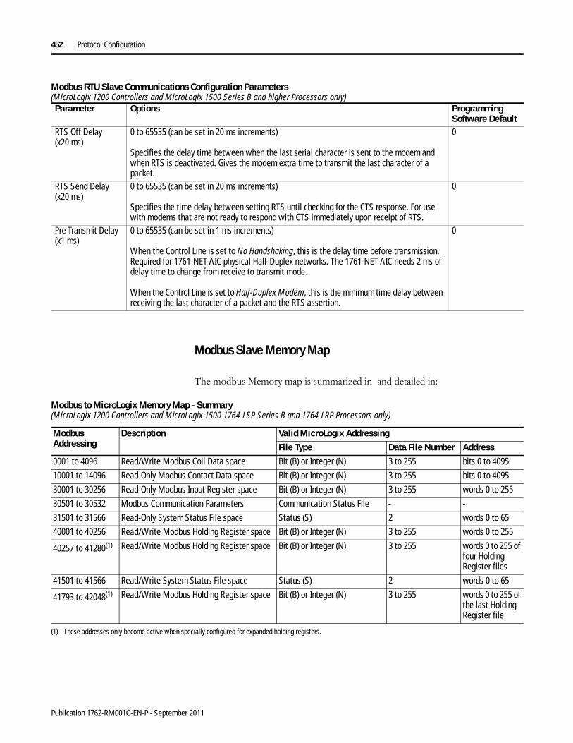
452 Protocol Configuration
Modbus Slave Memory Map
The modbus Memory map is summarized in and detailed in:
RTS Off Delay (x20 ms)
0 to 65535 (can be set in 20 ms increments)
Specifies the delay time between when the last serial character is sent to the modem and when RTS is deactivated. Gives the modem extra time to transmit the last character of a packet.
0
RTS Send Delay (x20 ms)
0 to 65535 (can be set in 20 ms increments)
Specifies the time delay between setting RTS until checking for the CTS response. For use with modems that are not ready to respond with CTS immediately upon receipt of RTS.
0
Pre Transmit Delay (x1 ms)
0 to 65535 (can be set in 1 ms increments)
When the Control Line is set to No Handshaking, this is the delay time before transmission. Required for 1761-NET-AIC physical Half-Duplex networks. The 1761-NET-AIC needs 2 ms of delay time to change from receive to transmit mode.
When the Control Line is set to Half-Duplex Modem, this is the minimum time delay between receiving the last character of a packet and the RTS assertion.
0
Modbus RTU Slave Communications Configuration Parameters (MicroLogix 1200 Controllers and MicroLogix 1500 Series B and higher Processors only)Parameter Options Programming
Software Default
Modbus to MicroLogix Memory Map - Summary(MicroLogix 1200 Controllers and MicroLogix 1500 1764-LSP Series B and 1764-LRP Processors only)
Modbus Addressing
Description Valid MicroLogix AddressingFile Type Data File Number Address
0001 to 4096 Read/Write Modbus Coil Data space Bit (B) or Integer (N) 3 to 255 bits 0 to 4095
10001 to 14096 Read-Only Modbus Contact Data space Bit (B) or Integer (N) 3 to 255 bits 0 to 4095
30001 to 30256 Read-Only Modbus Input Register space Bit (B) or Integer (N) 3 to 255 words 0 to 255
30501 to 30532 Modbus Communication Parameters Communication Status File - -
31501 to 31566 Read-Only System Status File space Status (S) 2 words 0 to 65
40001 to 40256 Read/Write Modbus Holding Register space Bit (B) or Integer (N) 3 to 255 words 0 to 255
40257 to 41280(1) Read/Write Modbus Holding Register space Bit (B) or Integer (N) 3 to 255 words 0 to 255 of four Holding Register files
41501 to 41566 Read/Write System Status File space Status (S) 2 words 0 to 65
41793 to 42048(1) Read/Write Modbus Holding Register space Bit (B) or Integer (N) 3 to 255 words 0 to 255 of the last Holding Register file
(1) These addresses only become active when specially configured for expanded holding registers.
Publication 1762-RM001G-EN-P - September 2011

Protocol Configuration 453
Modbus Slave to MicroLogix Memory Map - Detail(MicroLogix 1200 Controllers and MicroLogix 1500 1764-LSP Series B and 1764-LRP Processors only)
Modbus Addressing Modbus Address Reference Modbus Function Code (decimal)
0001 to 4096 Read/Write Modbus Coil Data space 1, 5, 15
10001 to 14096 Read Only Modbus Contact Data space 2
30001 to 30256 Read Modbus Input Register space 4
30501 Modbus Data Table Coil File Number 4
30502 Modbus Data Table Contact File Number 4
30503 Modbus Data Table Input Register File Number 4
30504 Modbus Data Table Holding Register File Number 4
30506 Pre-Send Delay 4
30507 Modbus Slave Address 4
30508 Inter-character Timeout 4
30509 RTS Send Delay 4
30510 RTS Off Delay 4
30511 Parity 4
30512 Presentation Layer Error Code 4
30512 Presentation Layer Error Code 4
30513 Presentation Layer Error Count 4
30514 Executed Function Code Error 4
30515 Last Transmitted Exception Code 4
30516 File Number of Error Request 4
30517 Element Number of Error Request 4
30518 Function Code 1 Message Counter - Read Single Output Coil 4
30519 Function Code 2 Message Counter - Read Discrete Input Image 4
30520 Function Code 3 Message Counter - Read Single Holding Register 4
30521 Function Code 4 Message Counter - Read Single Input Register 4
30522 Function Code 5 Message Counter - Set/Clear Single Output Coil 4
30523 Function Code 6 Message Counter - Read/Write Single Holding Register 4
30524 Function Code 8 Message Counter - Run Diagnostics 4
30525 Function Code 15 Message Counter - Set/Clear for Block of Output Coils 4
30526 Function Code 16 Message Counter - Read/Write for Block of Holding Registers 4
30527 Modem Status 4
30528 Total messages responded to by this slave 4
30529 Total messages to this Slave 4
30530 Total Messages Seen 4
30531 Link Layer Error Count 4
30532 Link Layer Error 4
31501 to 31566 Read Only System Status File 4
40001 to 40256 Read/Write Modbus Holding Register space (1st Holding Register file). 3, 6, 16
40257 to 40512 Read/Write Modbus Holding Register space (2nd Holding Register file). 3, 6, 16
40513 to 40768 Read/Write Modbus Holding Register space (3rd Holding Register file). 3, 6, 16
40769 to 41024 Read/Write Modbus Holding Register space (4th Holding Register file). 3, 6, 16
41025 to 41280 Read/Write Modbus Holding Register space (5th Holding Register file). 3, 6, 16
41501 to 41566 Read/Write System Status File 3, 6, 16
41793 to 42048 Read/Write Modbus Holding Register space (6th Holding Register file). 3, 6, 16
Publication 1762-RM001G-EN-P - September 2011
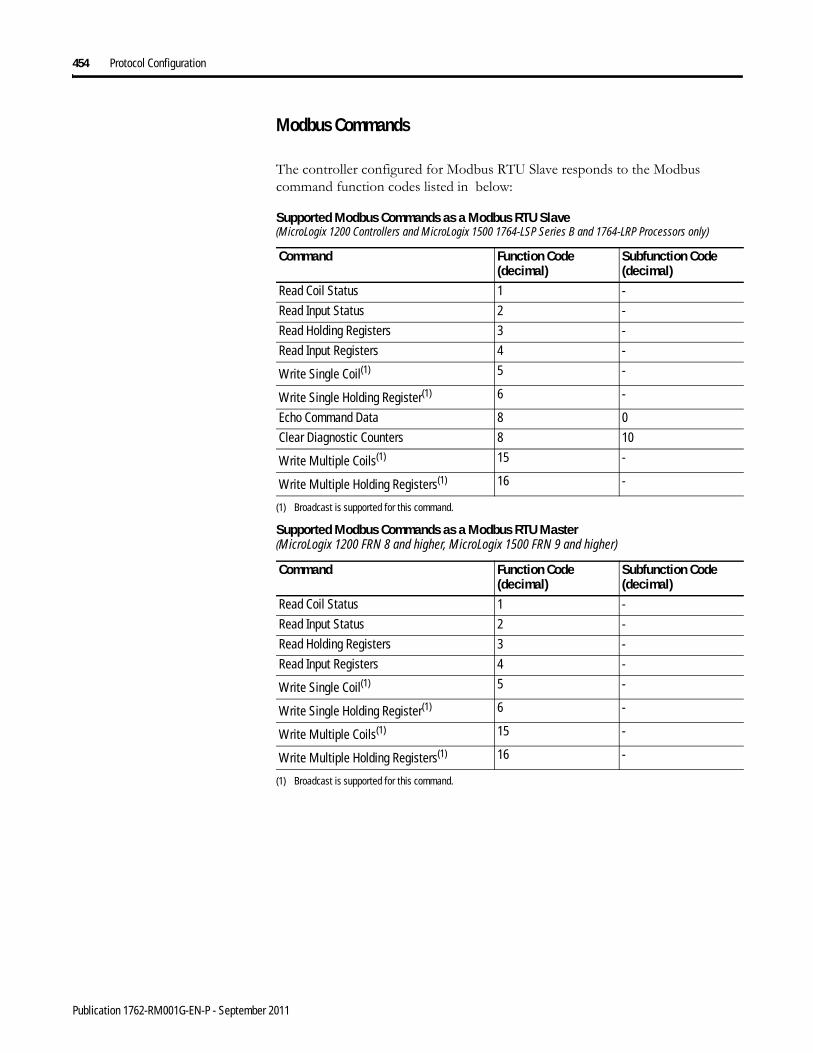
454 Protocol Configuration
Modbus Commands
The controller configured for Modbus RTU Slave responds to the Modbus command function codes listed in below:
Supported Modbus Commands as a Modbus RTU Slave(MicroLogix 1200 Controllers and MicroLogix 1500 1764-LSP Series B and 1764-LRP Processors only)
Command Function Code(decimal)
Subfunction Code(decimal)
Read Coil Status 1 -
Read Input Status 2 -
Read Holding Registers 3 -
Read Input Registers 4 -
Write Single Coil(1)
(1) Broadcast is supported for this command.
5 -
Write Single Holding Register(1) 6 -
Echo Command Data 8 0
Clear Diagnostic Counters 8 10
Write Multiple Coils(1) 15 -
Write Multiple Holding Registers(1) 16 -
Supported Modbus Commands as a Modbus RTU Master(MicroLogix 1200 FRN 8 and higher, MicroLogix 1500 FRN 9 and higher)
Command Function Code(decimal)
Subfunction Code(decimal)
Read Coil Status 1 -
Read Input Status 2 -
Read Holding Registers 3 -
Read Input Registers 4 -
Write Single Coil(1)
(1) Broadcast is supported for this command.
5 -
Write Single Holding Register(1) 6 -
Write Multiple Coils(1) 15 -
Write Multiple Holding Registers(1) 16 -
Publication 1762-RM001G-EN-P - September 2011

Protocol Configuration 455
Modbus Error Codes
Upon receiving a Modbus command that is not supported or improperly formatted, the controller configured for Modbus RTU Slave will respond with one of the exception codes listed below:
The following table lists the possible error codes and error descriptions for the Modbus RTU Master MSG Instruction.
Modbus Error Codes Returned by Modbus RTU Slave(MicroLogix 1200 Controllers and MicroLogix 1500 1764-LSP Series B and 1764-LRP Processors only)
Error Code
Error Description Transmitted Exception Code(1)
0 No error. none
1 Function Code cannot Broadcast. The function does not support Broadcast. nothing transmitted
2 Function Code not supported. The controller does not support this Modbus function or subfunction.
1
3 Bad Command Length. The Modbus Command is the wrong size. 3
4 Bad Length. The function attempted to read/write past the end of a data file. 3
5 Bad parameter The function cannot be executed with these parameters. 1
6 Bad File Type The file number being referenced is not the proper file type. 2
7 Bad File Number The file number does not exist 2
8 Bad Modbus Address The function attempted to access an invalid Modbus address.(2) 3
9 Table Write protected The function attempted to write to a read-only file. 3
10 File Access Denied Access to this file is not granted. 2
11 File Already Owned Data file is already owned by another process. 2
(1) If Modbus Command is sent with a valid Broadcast address, then no exception reply will be sent for Error Codes 2 through 11.
(2) See on page 452 for valid Modbus memory mapping.
Modbus Error Codes in Modbus RTU Master MSG Instruction(MicroLogix 1200 FRN 8 and higher, MicroLogix 1500 FRN 9 and higher)
Error Code
Error Description Received Exception Code
81 Illegal Function The function code sent by the Master is not supported by the slave or has an incorrect parameter.
1
82 Illegal Data Address The data address referenced in the Master command does not exist in the slave, or access to that address is not allowed.
2
83 Illegal Data Value The data value being written is not allowed, either because it is out of range, or it is being written to a read-only address.
3
84 Slave Device Failure An unrecoverable error occurred while the slave was attempting to perform the requested action.
4
85 Acknowledge The slave has accepted the request, but a long duration of time will be required to process the request.
5
86 Slave Device Busy The slave is currently processing a long-duration command. 6
Publication 1762-RM001G-EN-P - September 2011

456 Protocol Configuration
When Channel 0 or Channel 1 is configured for Modbus RTU Master or Modbus RTU Slave, the associated Channel Status screen displays a Link Layer Error Count and a Link Layer Error Code. Use the table below to interpret the Link Layer Error Code being displayed.
ASCII Driver The ASCII driver provides connection to other ASCII devices, such as bar code readers, weigh scales, serial printers, and other intelligent devices.
You can use ASCII by configuring the RS-232 port, channel 0 for ASCII driver (For the 1764-LRP only, you can select either Channel 0 or Channel 1). When configured for ASCII, all received data is placed in a buffer. To access the data, use the ASCII instructions in your ladder program. See ASCII Instructions on page 279 for information on using the ASCII instructions. You can also send ASCII string data to most attached devices that accept ASCII data/characters.
87 Negative Acknowledge The slave cannot perform the program function received in the command.
7
88 Memory Parity Error The slave attempted to read extended memory, but detected a parity error in the memory.
8
89 Non-standard Error Code An error code greater than 8 was returned by the slave. >8
Modbus Error Codes in Modbus RTU Master MSG Instruction(MicroLogix 1200 FRN 8 and higher, MicroLogix 1500 FRN 9 and higher)
Error Code
Error Description Received Exception Code
Modbus RTU Link Layer Error Codes
Error Code Description0 No error.
1 No receive buffer available for reply.
2 Too short message received.
3 Too long message received.
4 UART error during reply reception.
5 Bad CRC in reply packet.
6 CTS one-second timeout prior to transmission.
7 CTS dropped in mid-packet transmission.
9 Packet receive from unknown slave or bad slave.
10 Function code mismatch.
11 Function code not supported.
13 Reply timeout.
TIP Only ASCII instructions can be used when a channel is configured for ASCII. If you use a Message (MSG) instruction that references the channel, an error occurs.
Publication 1762-RM001G-EN-P - September 2011

Protocol Configuration 457
The channel configuration screen is shown below:
The controller updates changes to the channel configuration at the next execution of a Service Communications (SVC) instruction, I/O Refresh (REF) instruction, or when it performs Communications Servicing, whichever comes first.
When the driver is set to ASCII, the following parameters can be changed:
ASCII Channel Configuration Parameters(MicroLogix 1200; MicroLogix 1500 1764-LSP Series B and higher, and MicroLogix 1500 1764-LRP)
Parameter Description Programming Software Default
Channel MicroLogix 1200, and MicroLogix 1500 1764-LSP Series B and higher: Channel 0
MicroLogix 1500 1764-LRP: Channel 0 or 1
0 (1200 & LSP)
0 or 1 (LRP)
Driver ASCII
Baud Rate Toggles between the communication rate of 300, 600, 1200, 2400, 4800, 9600, 19.2K, and 38.4K. 1200
Parity Toggles between None, Odd, and Even. None
Termination 1 Specifies the first termination character. The termination character defines the one or two character sequence used to specify the end of an ASCII line received. Setting the first ASCII termination character to undefined (\ff) indicates no ASCII receiver line termination is used.
\d
Termination 2 Specifies the second termination character. The termination character defines the one or two character sequence used to specify the end of an ASCII line received. Setting the second ASCII Termination character to undefined (\ff) and the first ASCII Termination character to a defined value (\d) indicates a single character termination sequence.
\ff
Control Line Toggles between No Handshaking, Half-Duplex Modem, and Full-Duplex Modem No Handshaking
Publication 1762-RM001G-EN-P - September 2011
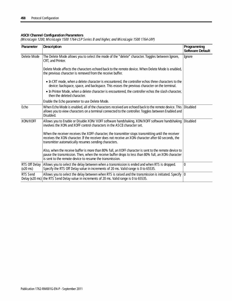
458 Protocol Configuration
Delete Mode The Delete Mode allows you to select the mode of the “delete” character. Toggles between Ignore, CRT, and Printer.
Delete Mode affects the characters echoed back to the remote device. When Delete Mode is enabled, the previous character is removed from the receive buffer.
• In CRT mode, when a delete character is encountered, the controller echos three characters to the device: backspace, space, and backspace. This erases the previous character on the terminal.
• In Printer Mode, when a delete character is encountered, the controller echos the slash character, then the deleted character.
Enable the Echo parameter to use Delete Mode.
Ignore
Echo When Echo Mode is enabled, all of the characters received are echoed back to the remote device. This allows you to view characters on a terminal connected to the controller. Toggles between Enabled and Disabled.
Disabled
XON/XOFF Allows you to Enable or Disable XON/ XOFF software handshaking. XON/XOFF software handshaking involves the XON and XOFF control characters in the ASCII character set.
When the receiver receives the XOFF character, the transmitter stops transmitting until the receiver receives the XON character. If the receiver does not receive an XON character after 60 seconds, the transmitter automatically resumes sending characters.
Also, when the receive buffer is more than 80% full, an XOFF character is sent to the remote device to pause the transmission. Then, when the receive buffer drops to less than 80% full, an XON character is sent to the remote device to resume the transmission.
Disabled
RTS Off Delay (x20 ms)
Allows you to select the delay between when a transmission is ended and when RTS is dropped. Specify the RTS Off Delay value in increments of 20 ms. Valid range is 0 to 65535.
0
RTS Send Delay (x20 ms)
Allows you to select the delay between when RTS is raised and the transmission is initiated. Specify the RTS Send Delay value in increments of 20 ms. Valid range is 0 to 65535.
0
ASCII Channel Configuration Parameters(MicroLogix 1200; MicroLogix 1500 1764-LSP Series B and higher, and MicroLogix 1500 1764-LRP)
Parameter Description Programming Software Default
Publication 1762-RM001G-EN-P - September 2011

Appendix F
Knowledgebase Quick Starts
The following Quick Start topics are included:
• 17583 “Quick Start” Pulse Train Output (PTO) on page 459• 17585 “Quick Start” Pulse Width Modulation (PWM) on page 462• 17586 “Quick Start” High Speed Counter (HSC) on page 463• 17605 “Quick Start” Message (MSG) on page 468• 17653 “Quick Start” Selectable Timed Interrupt (STI) on page 471• 17655 “Quick Start” Real Time Clock (RTC) on page 473• 17657 “Quick Start” Trim Pots on page 475• 17712 “Quick Start” User Interrupt Disable (UID) on page 477• 18689 “Quick Start” RTC Synchronization Between Controllers on page 478• 18728 “Quick Start” Data Logging (DLG) on page 481
17583 “Quick Start” Pulse Train Output (PTO)
Locate the Function Files under Controller in RSLOGIX 500 v4.00 or later and select the PTO tab, then select the [+] next to PTO:0 (See Below).
TIP The PWM function is only available when using the BXB models of the MicroLogix 1200 or 1500
459 Publication 1762-RM001G-EN-P - September 2011

460 Knowledgebase Quick Starts
Enter the following parameters as the “Minimum Configuration” required for the PTO to generate pulses.
Example
The following example will generate 10,000 pulses on Output O:0/2 at a frequency of 500Hz and 100 pulses will be used for Accelerating and 100 pulses will be used for Decelerating.
PTO:0.OUT Select Destination Output for pulses: Output O:0/2 or O:0/3PTO:0.OF Output Frequency - Frequency of pulses: 0 to 20,000 Hz
Data less then zero and greater then 20,000 generates a PTO errorPTO:0.TOP Total Output Pulses - Determines total number of pulses to be
generated by the controllerPTO:0.ADP Accel/Decel Pulses - How many of the total pulses will be used for
the Accel/Decel component
Publication 1762-RM001G-EN-P - September 2011

Knowledgebase Quick Starts 461
The following ladder logic will need to be entered into File #2
By toggling Bit B3/0 the PTO can be activated. Once running the PTO will generate the number of pulses entered into the PTO:0.TOP word and then stop. To restart, toggle B3/0.
General Information on the PTO
Once running the PTO will continue to generate pulses until all pulses have been generated or the PTO:0/EH (Enable Hard Stop) bit has been activated.
Once the EH bit is set the instruction will generate a PTO error of 1 (hard stop detected). In order to clear this error the PTO instruction must be scanned on a false rung of logic, and the EH bit must be off.
To change the Total Output Pulses Generated in a working program a new value can be moved into PTO:0.TOP by using the MOV command.
IMPORTANT Once the PTO has been initiated and is generating pulses a new TOP value will not take effect until the PTO has either completed generating pulses and has been restarted or has been Hard Stopped using PTO:0/EH bit and been restarted.
Publication 1762-RM001G-EN-P - September 2011
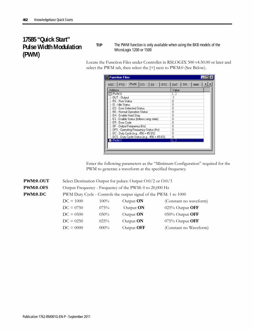
462 Knowledgebase Quick Starts
17585 “Quick Start” Pulse Width Modulation (PWM)
Locate the Function Files under Controller in RSLOGIX 500 v4.50.00 or later and select the PWM tab, then select the [+] next to PWM:0 (See Below).
Enter the following parameters as the “Minimum Configuration” required for the PWM to generate a waveform at the specified frequency.
TIP The PWM function is only available when using the BXB models of the MicroLogix 1200 or 1500
PWM:0.OUT Select Destination Output for pulses: Output O:0/2 or O:0/3PWM:0.OFS Output Frequency - Frequency of the PWM: 0 to 20,000 HzPWM:0.DC PWM Duty Cycle - Controls the output signal of the PWM: 1 to 1000
DC = 1000 100% Output ON (Constant no waveform)DC = 0750 075% Output ON 025% Output OFF
DC = 0500 050% Output ON 050% Output OFF
DC = 0250 025% Output ON 075% Output OFF
DC = 0000 000% Output OFF (Constant no Waveform)
Publication 1762-RM001G-EN-P - September 2011

Knowledgebase Quick Starts 463
Example
The following example will generate a waveform on Output O:0/2 at a frequency of 250Hz and a 50% Duty Cycle.
The following ladder logic will need to be entered into File #2
By toggling Bit B3/0 the PWM can be activated.
17586 “Quick Start” High Speed Counter (HSC)
General Information
The MicroLogix 1200 has one 20Khz high-speed counter. The counter has four dedicated inputs that are isolated from all other inputs on the unit. The HSC can utilize inputs 0 through 3. Input device connection depends on the counter mode selected. The MicroLogix 1200 uses a 32-bit signed integer for the HSC this allows for a count range of (+/-) 2,147,483,647.
TIP Once activated the PWM will continue to generate a waveform until B3/0 is toggled OFF or the PWM:0/EH (Enable Hard Stop) bit has been activated.
Publication 1762-RM001G-EN-P - September 2011

464 Knowledgebase Quick Starts
The MicroLogix 1500 has two 20Khz high-speed counters. Each counter has four dedicated inputs that are isolated from all other inputs on the base unit HSC:0 can utilize inputs 0 through 3, and HSC: 1 can utilize inputs 4 through 7. Input device connection depends on the counter mode selected. Each counter is completely independent and isolated from the other. The MicroLogix 1500 uses a 32-bit signed integer for the HSC this allows for a count range of (+/-) 2,147,483,647.
Getting Started
Locate the Function Files under Controller in RSLOGIX 500 and select the HSC tab, then select the [+] next to HSC:0 (See Below)
Enter the following parameters for the “Minimum Configuration” required for the HSC to count pulses.
TIP There is no additional ladder logic required to enable the High Speed Counter. In other words there is no HSC instruction needed for the ladder logic program
HSC:0.PFN Program File Number defines which subroutine is executed when the HSC:0 accumulated count equals the High or Low preset or passes through Overflow or Underflow. The Integer number entered must be a valid sub-routine program file (3 to 255).
HSC:0/AS Auto-Start defines if the HSC function will automatically start when the MicroLogix enters run or test.
HSC:0/CE Counting Enabled control bit is used to enable or disable the HSCHSC:0.HIP High Preset is the upper set point (in counts) that defines when the HSC will generate an
interrupt and execute the PFN sub-routine.
Publication 1762-RM001G-EN-P - September 2011
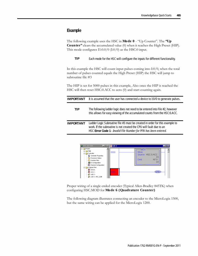
Knowledgebase Quick Starts 465
Example
The following example uses the HSC in Mode 0 - “Up Counter”. The “Up Counter” clears the accumulated value (0) when it reaches the High Preset (HIP). This mode configures I1:0.0/0 (I:0/0) as the HSC:0 input.
In this example the HSC will count input pulses coming into I:0/0, when the total number of pulses counted equals the High Preset (HIP) the HSC will jump to subroutine file #3
The HIP is set for 5000 pulses in this example, Also once the HIP is reached the HSC will then reset HSC:0.ACC to zero (0) and start counting again.
Proper wiring of a single ended encoder (Typical Allen-Bradley 845TK) when configuring HSC.MOD for Mode 6 (Quadrature Counter)
The following diagram illustrates connecting an encoder to the MicroLogix 1500, but the same wiring can be applied for the MicroLogix 1200.
TIP Each mode for the HSC will configure the inputs for different functionality.
IMPORTANT It is assumed that the user has connected a device to I:0/0 to generate pulses.
TIP The following ladder logic does not need to be entered into File #2, however this allows for easy viewing of the accumulated counts from the HSC:0.ACC.
IMPORTANT Ladder Logic Subroutine file #3 must be created in order for this example to work. If the subroutine is not created the CPU will fault due to an HSC Error Code 1 - Invalid File Number for PFN has been entered.
Publication 1762-RM001G-EN-P - September 2011
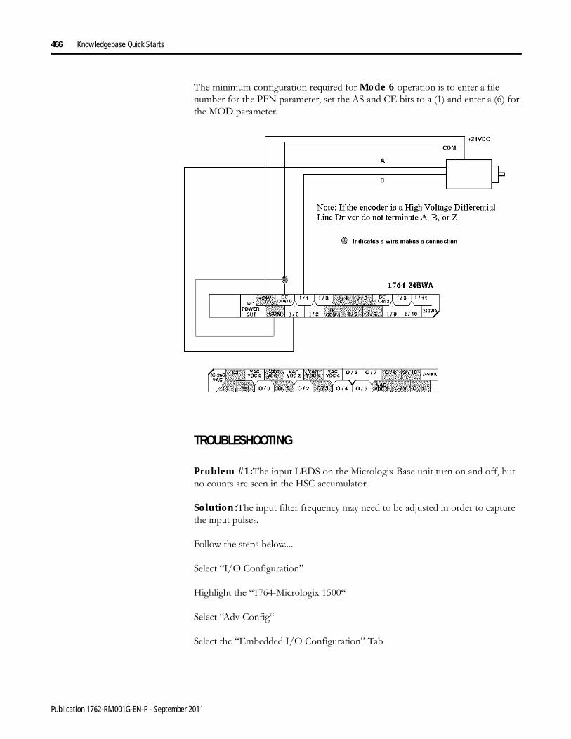
466 Knowledgebase Quick Starts
The minimum configuration required for Mode 6 operation is to enter a file number for the PFN parameter, set the AS and CE bits to a (1) and enter a (6) for the MOD parameter.
TROUBLESHOOTING
Problem #1:The input LEDS on the Micrologix Base unit turn on and off, but no counts are seen in the HSC accumulator.
Solution:The input filter frequency may need to be adjusted in order to capture the input pulses.
Follow the steps below....
Select “I/O Configuration”
Highlight the “1764-Micrologix 1500“
Select “Adv Config“
Select the “Embedded I/O Configuration” Tab
Publication 1762-RM001G-EN-P - September 2011

Knowledgebase Quick Starts 467
Adjust Input filters as needed
Problem #2: The HSC instruction does not accumulate counts and the Error Code (ER) shows a value of (1).
Solution:A file number was entered into (PFN) but the value entered was less then (3) or greater then (255) or the file number entered was correct, however the file does not exist.
Create the NEW program file by “Right” mouse clicking on “Program Files”
Problem #3: Some of my outputs will not turn On or Off when the ladder logic appears to indicate that they should.
Solution:OMB (Output Mask Bits). Verify what the OMB has been configured for in the HSC function file. If an output(s) has been assigned to the HSC for control, then the output(s) will not be controlled anywhere else in the ladder program. Only the HSC will have control over these outputs.
Publication 1762-RM001G-EN-P - September 2011

468 Knowledgebase Quick Starts
17605 “Quick Start” Message (MSG)
Communications Specifications:
The MicroLogix 1200 & 1500 processors contain a total of (12) Message Buffers.
The Outgoing queue also supports unlimited queuing. This means that even if a buffer is not available the MSG will simply wait until one of the outgoing buffers becomes available and then transmit.
How quickly a message is actually sent or received to/by a destination device depends on a number of issues, including the selected channels communication protocol, baud rate of the communications port, number of retries, destination devices readiness to receive, ladder logic scan time, etc.
Definition of the Message (MSG) instruction:
The message instruction (MSG) is an output instruction which when configured correctly allows data to be sent or received to other compatible devices.
The MSG instruction in the MicroLogix 1200/1500 controller uses a Data File MG to process the message instruction. All message elements are accessed using the MG prefix (example: MSG done bit = MG11:0/DN).
Continuous Message Example:
The following example illustrates how, by using the MSG Done (DN) and Error (ER) bits to unlatch the Enable (EN) bit the MSG instruction can be configured for continuous execution.
This example uses MG11:0 for the MSG file and will require two MicroLogix controllers one a ML1500 and the other either a ML1000 or ML1500. The ML1500 will need to be configured as Node 1 and the other processor as node 4.
(8) Incoming Any incoming MSG's, Communications, and/or responses to a command the ML1200/1500 initiated.
(4) Outgoing Any outgoing MSG's, Communications and/or responses to incoming request for data.
TIP If a message has been waiting in the queue, at the moment of buffer availability, the most current data will be sent, not the data that was available at the time the message instruction was first scanned true.
Publication 1762-RM001G-EN-P - September 2011
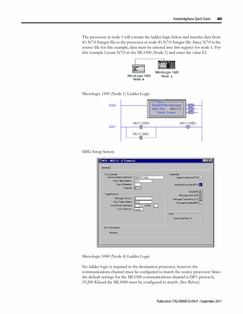
Knowledgebase Quick Starts 469
The processor at node 1 will contain the ladder logic below and transfer data from it's N7:0 Integer file to the processor at node 4's N7:0 Integer file. Since N7:0 is the source file for this example, data must be entered into this register for node 1. For this example Locate N7:0 in the ML1500 (Node 1) and enter the value 63.
Micrologix 1500 (Node 1) Ladder Logic
MSG Setup Screen
Micrologix 1000 (Node 4) Ladder Logic
No ladder logic is required in the destination processor, however the communications channel must be configured to match the source processor. Since the default settings for the ML1500 communications channel is DF1 protocol, 19,200 Kbaud the ML1000 must be configured to match. (See Below)
Publication 1762-RM001G-EN-P - September 2011

470 Knowledgebase Quick Starts
Micrologix 1000 Channel Configuration
Verifying data has been sent:
To verify the data has been sent to node 4 disconnect the HM02 cable and connect the PC running RSLogix 500 to the ML1000 (Node 4). Go to N7:0 and view the data, this should match the data in N7:0 of node 1.
Another way to verify the data is being sent to node 4 is to replace the Target Device Data Table Address with an output modules address. In this example the output module is a ML1000, the address would be O:0.0 This will display, in binary on the output LEDS, what ever number that was entered into N7:0 of the ML1500.
If a 16 Point MicroLogix 1000 is being used as the destination processor (Node 1), and the number 63 is entered into the above example, all the outputs will be energized or turn. If the number entered is greater then 63 then a fault may occur with an error stating that the extended I/O bit (S:0/8) was not set. In this case clear the fault, go offline, set bit (S:0/8) and re-download the ladder program.
The above example uses the DF1 Full Duplex protocol. This is a point to point or One Device to One Device protocol, using this protocol no other devices can be connected. To create a network of multiple processors or devices use the DH485 protocol and 1761-NET-AIC devices.
IMPORTANT After the ladder logic has been entered into the ML1500 and the ML1000 channel configuration has been changed, in order for this example to function connect the controllers using a 1761-CBL-HM02 cable, leave connected until the COMM 0 LED on the ML1500 starts to blink.
IMPORTANT By addressing O:0.0 the outputs of the destination processor will be energized upon successful transmission of data. Verify that nothing is connected to the outputs to ensure safe operation of the controller.
TIP This example was written using a ML1500 communicating to a ML1000, however any DF1 or DH485 device could have been substituted for the ML1000. (i.e. MicroLogix 1200, SLC 5/03, 5/04, 5/05, PLC-5, Bar Code Scanners, etc.)
Publication 1762-RM001G-EN-P - September 2011

Knowledgebase Quick Starts 471
17653 “Quick Start” Selectable Timed Interrupt (STI)
What is an Interrupt?
An interrupt is an event that causes the processor to suspend the task it is currently performing, perform a different task, and then return to the suspend task at the point where it suspended.
STI Definition
The STI provides a mechanism to solve time critical control requirements. The STI is a trigger mechanism that allows you to scan or solve control program logic that is time sensitive.
Example: A Block of logic that needs to be scanned more often then the rest of the ladder program.
Getting Started:
Locate the Function Files under Controller in RSLOGIX 500 v4.00 or later and select the STI tab (See Below)
Enter the following parameters as the “Minimum Configuration” required for the STI
STI:0.PFN Program File Number defines which subroutine is executed when the SPM value has timed out. The Integer number entered must be a valid sub-routine program file (3 to 255).
STI:0/AS Auto-Start defines if the STI function will automatically start when the MicroLogix 1500 enters run or test.
Publication 1762-RM001G-EN-P - September 2011

472 Knowledgebase Quick Starts
Example
The following example configures the STI to execute sub-routine file #3 (PFN=3) every 2 seconds (SPM=2000). In the subroutine file there is an ADD instruction simply adding the value of 1 to N7:0 each time the sub-routine is scanned.
This example also sets the User Interrupt Enable bit and the Auto Start bit allowing the STI to execute.
STI:0/UIE User Interrupt Enabled control bit is used to enable or disable the STI subroutine from processing.
STI:0.SPM Setpoint (in milliseconds) defines the interval that the interrupt will scan the PFN sub-routine.
IMPORTANT Ladder Logic Subroutine file #3 must be created in order for this example to work. If the subroutine is not created the CPU will fault due to a STI Error Code 1 - Invalid File Number for PFN has been entered.
Publication 1762-RM001G-EN-P - September 2011

Knowledgebase Quick Starts 473
Notes on using Interrupt bits
If the Auto Start bit (AS) is set this will start the interrupt on power up and set the Timed Interrupt Enabled bit (TIE) automatically, allowing the interrupt to execute. Shown in the above example.
If the AS bit is not set then the TIE bit must be set through the ladder logic in order for the interrupt to execute.
The User Interrupt Enable bit (UIE) determines if the interrupt executes or not.
17655 “Quick Start” Real Time Clock (RTC)
General Information:
The RTC provides Year, Month, Day, Day of Month, Day of Week, Hour, Minute, and Second information to the RTC Function file in the controller.
The RTC module is located in the processor unit, under the processor cover (Shown Below). Like the Memory Module the RTC can be removed or inserted under power without risk of damage to the RTC or the processor module. If the module is installed while the ML1200/1500 is executing, the module will not be recognized until a power cycle occurs or the controller is placed into program mode or faults.
ML1200 ML1500
Publication 1762-RM001G-EN-P - September 2011
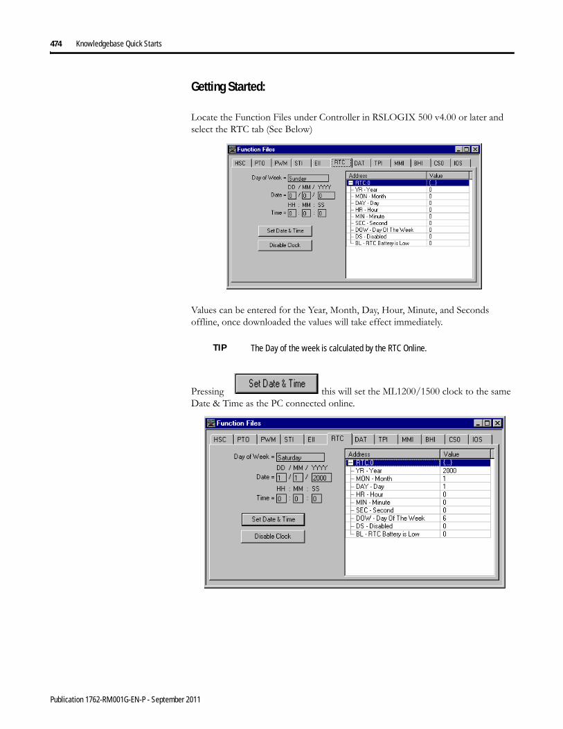
474 Knowledgebase Quick Starts
Getting Started:
Locate the Function Files under Controller in RSLOGIX 500 v4.00 or later and select the RTC tab (See Below)
Values can be entered for the Year, Month, Day, Hour, Minute, and Seconds offline, once downloaded the values will take effect immediately.
Pressing this will set the ML1200/1500 clock to the same Date & Time as the PC connected online.
TIP The Day of the week is calculated by the RTC Online.
Publication 1762-RM001G-EN-P - September 2011

Knowledgebase Quick Starts 475
Pressing will disable the RTC from functioning and decrease the drain on the battery during storage.
17657 “Quick Start” Trim Pots
General
On the ML1200 the trim pots are located next to the communication port. On the ML1500 the trim pots are located below the mode switch under the left access door of the processor. Each of the trim pots can be used to manipulate data within the controller. The data value of the trim pots can be used throughout the control program as timer, counter, analog presets, etc.
ML1200 ML1500
Adjust the trim pots using a small flathead screwdriver. By turning the trim pot the data will change within a range of 0 to 250 (fully clockwise). The maximum rotation of each pot is three quarters of a turn.
RTC:0/BL The Battery Low bit will be set (1) when the battery is low. This means that the battery will fail in less than 14 Days after which the RTC data may become invalid. At this time the RTC module will need to be replaced.
Publication 1762-RM001G-EN-P - September 2011

476 Knowledgebase Quick Starts
Getting Started:
Locate the Function Files under Controller in RSLOGIX 500 v4.00 or later and select the TPI tab (See Below)
There is no configuration needed for the trim pots. The values are read only. While online, turn the trim pots and watch the values change.
Trim Pot Example Ladder Logic
The following example will MOVe the value from trim pot 0 (POT0) into the preset word of the “free running” timer at T4:0
Using a trim pot to adjust a value larger then 250
By using the SCP instruction a ladder program can be written which will allow the trim pot to adjust between: -32768 to 32767 using standard word -2,147,483,648 to 2,147,483,647 using long words
TIP Since the trim pots only adjust from 0 to 250 the timer preset is only adjustable from 0 to 250 seconds.
IMPORTANT Remember that the trim pots only have 3/4 of a turn resolution.
Publication 1762-RM001G-EN-P - September 2011

Knowledgebase Quick Starts 477
The following example takes the input value of trim pot 0 (0 - 250) and scales it from 0 to 600 using the Scale with Parameters instruction (SCP). The scaled value is placed in the preset of the “free running” timer at T4:0. This allows for POT 0 to adjust from 0 to 10 minutes (600 Sec.).
17712 “Quick Start” User Interrupt Disable (UID)
The UID instruction can be used as an output instruction to disable selected user interrupts.
Once a user interrupt is disabled the User Interrupt Enable bit (UIE) for the selected interrupt will be cleared or reset to a zero (0). This stops the interrupt from executing.
To re-enable an interrupt the UIE bit must be set to a one (1), or a UIE instruction must be used.
The following table indicates the types of interrupts disabled by the UID.
To disable interrupt(s) follow these steps....
1. Select which Interrupt(s) to disable from the above table.
2. Locate the decimal value for each Interrupt(s).
Publication 1762-RM001G-EN-P - September 2011
478 Knowledgebase Quick Starts
3. Add the decimal values together if more then one Interrupt was selected.
4. Enter the sum into the UID instruction.
For example, to disable EII Event 1 and EII Event 3....
EII Event 1 = 32 EII Event 3 = 04
32 + 04 = 36 (Enter this value in the UID instruction)
Notes on using Interrupt bits
If the Auto Start bit (AS) is set this will start the interrupt on power up and set the Timed Interrupt Enabled bit (TIE) automatically, allowing the interrupt to execute. Shown in the above example.
If the AS bit is not set then the TIE bit must be set through the ladder logic in order for the interrupt to execute.
The User Interrupt Enable bit (UIE) determines if the interrupt executes or not.
18689 “Quick Start” RTC Synchronization Between Controllers
The following example illustrates a message write from an SLC 5/03 or higher processor to a Micrologix 1500 processor with an installed RTC module that has been enabled.
This example can also be applied for messaging between Micrologix 1200 and 1500 controllers. When messaging from a Micrologix 1200/1500 controller to another Micrologix 1200/1500 it is recommended that RTC:0 be used as the source instead of (S:37 - S:42).
Minimum Hardware/Software requirements
Micrologix 1200 Series B FRN 2
Micrologix 1500 Series B FRN 4
RSLOGIX 500 is 4.10.00.02
Publication 1762-RM001G-EN-P - September 2011

Knowledgebase Quick Starts 479
Example
The example shows network connections using DH-485, however DF1 Full or Half Duplex will also work.
1) Configure the SLC's Channel 0 port for DH-485 protocol.
2) Enter the following ladder logic into the SLC processor.
Publication 1762-RM001G-EN-P - September 2011

480 Knowledgebase Quick Starts
The example above messages the SLC 500 Date and Time data (S:37 - S:42)to the Micrologix 1500 RTC, each time the SLC processor is powered up and placed into the RUN mode or each time the Time Synchronization Bit (B3:0/0) is enabled.
For each processor that requires its RTC to be synchronized a MSG write will be required. This is done simply by duplicating the above ladder logic, referencing a different Control Block (i.e. N100:0 = MSG1 | N100:20 = MSG2 | N100:40 = MSG3, etc.) and specifying a different node address in the MSG set-up screen.
ATTENTION: Valid years for the Micrologix 1200 and 1500 begin with 1998. Any date/time/year values, prior to 1998, that are sent to a Micrologix controller will generate a MSG Error Code 10h.
Publication 1762-RM001G-EN-P - September 2011

Knowledgebase Quick Starts 481
18728 “Quick Start” Data Logging (DLG)
General Information
The Data logging feature allows the creation of memory queues to capture or store application data as a record for later retrieval. Each record is stored in a user-configured battery backed queue. The size of memory where queues are stored is 48K bytes, this is independent of the rest of the processor memory.
The Data logging feature allows the capture or storage of application data as a record for later retrieval. Each record is stored in a user-configured battery backed queue. The size of the queue is 48K bytes, independent of the rest of the processor memory.
Configuring the DLG instruction in the Micrologix 1500 (LRP)
1. Create a new RSLogix 500 project for the 1764-LRP processor
2. Create a new rung of ladder logic in File 2 as shown below.
FYI - The DLG instruction ONLY captures data on a false-to-true rung transition.
Publication 1762-RM001G-EN-P - September 2011

482 Knowledgebase Quick Starts
3. Double Click Data Logging - Configuration in the controller organizer to access the Data Log Queue Configuration window
FYI - Every time Configuration above is double-clicked a new queue is added. To delete queues, simply select the queue with the mouse and press the <delete> key on the keyboard.
4. Double-Click on Data Log configuration to open the Configuration window.
Publication 1762-RM001G-EN-P - September 2011

Knowledgebase Quick Starts 483
5. Complete the Data Log Queue as shown below. The Number of records and Addresses selected were arbitrary for this example.
6. Click OK when completed
7. Click OK and accept the Data Log Que window
8. Once the N10 file has been created enter the following values for each
9. Download the program to your MicroLogix 1500 LRP.
10. Go On-Line
11. Toggle the Data Logging Enable(B3:0/0) bit Off to On a total of 5 times.
IMPORTANT Integer file N10 must be created with a length of 5 or the software will not compile the ladder program. Also a 1764-RTC, 1764-MM1RTC, 1764-MM2RTC must be installed and configured if the Date and Time stamp are to be used. If an RTC module is not installed & configured the data for these fields will contain zeros.
Publication 1762-RM001G-EN-P - September 2011

484 Knowledgebase Quick Starts
Using the Data Logging Utility Software to recover data
The Data Logging utility is the only supported method for retrieving data, that has been stored in the processor.
1. Install the DLOG utility (found at http://www.ab.com/plclogic/micrologix/)
2. Execute DLCA1764.EXE
3. Configure Port, Baud Rate, and DF1 Node as shown below.
4. Click “Connect”.
FYI - By default the MicroLogix 1500 communications are configured for 19200 baud If using defaults select 19200 above, otherwise select the baud rate configured in the MicroLogix Channel Configuration Screen.
If a correct configuration has been selected the utility software will indicate that it has connected to the processor as shown below.
5. Click Read Status once a valid connection is established
ATTENTION: If any other software package, such as RSLINX has control of the computers communication port or if the wrong COM port is selected or a processor other then the 1764-LRP is connected to the computer you will not be able to continue.
Publication 1762-RM001G-EN-P - September 2011
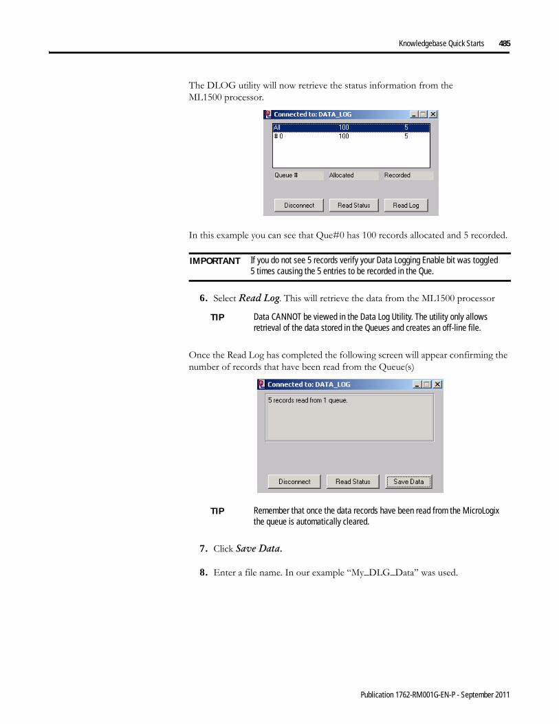
Knowledgebase Quick Starts 485
The DLOG utility will now retrieve the status information from the ML1500 processor.
In this example you can see that Que#0 has 100 records allocated and 5 recorded.
6. Select Read Log. This will retrieve the data from the ML1500 processor
Once the Read Log has completed the following screen will appear confirming the number of records that have been read from the Queue(s)
7. Click Save Data.
8. Enter a file name. In our example “My_DLG_Data” was used.
IMPORTANT If you do not see 5 records verify your Data Logging Enable bit was toggled 5 times causing the 5 entries to be recorded in the Que.
TIP Data CANNOT be viewed in the Data Log Utility. The utility only allows retrieval of the data stored in the Queues and creates an off-line file.
TIP Remember that once the data records have been read from the MicroLogix the queue is automatically cleared.
Publication 1762-RM001G-EN-P - September 2011
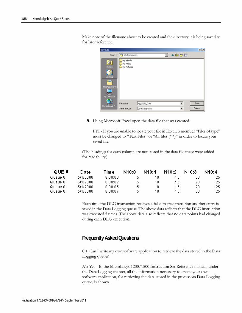
486 Knowledgebase Quick Starts
Make note of the filename about to be created and the directory it is being saved to for later reference.
9. Using Microsoft Excel open the data file that was created.
FYI - If you are unable to locate your file in Excel, remember “Files of type” must be changed to “Text Files” or “All files (*.*)” in order to locate your saved file.
(The headings for each column are not stored in the data file these were added for readability.)
Each time the DLG instruction receives a false-to-true transition another entry is saved in the Data Logging queue. The above data reflects that the DLG instruction was executed 5 times. The above data also reflects that no data points had changed during each DLG execution.
Frequently Asked Questions
Q1: Can I write my own software application to retrieve the data stored in the Data Logging queue?
A1: Yes - In the MicroLogix 1200/1500 Instruction Set Reference manual, under the Data Logging chapter, all the information necessary to create your own software application, for retrieving the data stored in the processors Data Logging queue, is shown.
Publication 1762-RM001G-EN-P - September 2011

Knowledgebase Quick Starts 487
Q2: Can the MicroLogix 1500 - LRP processor automatically send the information stored in the Data Logging queue directly to a printer?
A2: No - To retrieve the data either the free Data Logging Utility software must be used or a custom application must be created by the user. If the data does not need to be stored in the processor, but sent directly to a printer then use the ASCII instructions of the MicroLogix processor to send out the data.
Using the DATALOG Utility to retrieve data remotely via a Remote Access Modem Kit (RAD)
For more information on Remote Access Modem Kits visit http://support.rockwellautomation.com/modem/modem_Main.asp
The following outlines the configuration and steps that can be used to read data log records from an MicroLogix 1500 (1764-LRP) controller remotely via a 1747CH0RAD (Remote Access Modem Kit)
This example assumes that the programmer has configured the DLG instruction in the ML1500 to log data and that HyperTerminal is installed, configured and the user is familiar with its use.
ESTABLISHING CONNECTIONS
1. Connect the modem to Channel 1 of the 1764-LRP
2. Configure Channel 1 (9-Pin) for DF1 Full Duplex, 9600 baud, no parity, and full duplex modem handshaking. This setting is critical, as the system will not communicate if full duplex modem handshaking isn't applied to the comms channel connected to the modem.
3. Configure HyperTerminal for direct connection to the PC COMM port the modem is connected to. Make sure the HyperTerminal connection is configured for 9600 baud.
4. Save configuration as “DataLog “.
5. Send the following dial-out string using HyperTerminal to dial the modem and establish the connection:
Publication 1762-RM001G-EN-P - September 2011

488 Knowledgebase Quick Starts
AT&C1DT(Phone number of destination Modem) then press enter
your modem will respond: CONNECT 9600
Once the connection is established, exit HyperTerminal by selecting File/Exit from the pull-down menu. When asked “Do you want to close connection” select Yes. This will only close the connection from HyperTerminal to the RS-232 port. The connection will remain active.
FYI - It will appear as though HyperTerminal has disconnected. It has not; the connection is still established only HyperTerminal is no longer running.
6. Open the Data Logging Utility.
7. Select in the DLG Utility the COMM port that the PC modem is configured for.
8. Click Connect.
DISCONNECTING MODEM
1. 1. Ensure the DLG Utility has been shutdown.
2. 2.Start HyperTerminal (Do not re-connect)
3. 3.Open the previously configured “Datalog “
4. Type “+++” to place modem in command mode,
Do not press the ENTER KEY!
Your modem will respond: OK
5. Type “ATH “
6. Press Enter. This will send the disconnect command to modem.
Publication 1762-RM001G-EN-P - September 2011

Glossary
The following terms are used throughout this manual. Refer to the Allen-Bradley Industrial Automation Glossary, Publication Number AG-7.1, for a complete guide to Allen-Bradley technical terms.
address
A character string that uniquely identifies a memory location. For example, I:1/0 is the memory address for data located in Input file word 1, bit 0.
AIC+ Advanced Interface Converter
A device that provides RS-232 isolation to an RS-485 Half-Duplex communication link. (Catalog Number 1761-NET-AIC.)
application
1) A machine or process monitored and controlled by a controller. 2) The use of computer- or processor-based routines for specific purposes.
ASCII
American Standard Code for Information Interchange. A standard for defining codes for information exchange between equipment produced by different manufacturers. The basis of character sets used in most microcomputers; a string of 7 binary digits represents each character.
baud rate
The speed of communication between devices. Baud rate is typically displayed in K baud. For example, 19.2K baud = 19,200 bits per second.
bit
The smallest unit of memory used in discrete or binary logic, where the value 1 represents ON and 0 represents OFF.
block diagrams
A method used to illustrate logic components or a sequence of events.
Boolean operators
Logical operators such as AND, OR, NAND, NOR, NOT, and Exclusive-OR that can be used singularly or in combination to form logic statements or circuits. Can have an output response of T or F.
489 Publication 1762-RM001G-EN-P - September 2011
490 Glossary
branch
A parallel logic path within a rung of a ladder program. Its primary use is to build OR logic.
communication scan
A part of the controller’s operating cycle. Communication with devices (such as other controllers and operator interface devices) takes place during this period.
control program
User logic (the application) that defines the controller’s operation.
controller
A device, such as a programmable controller, used to control output devices.
controller overhead
A portion of the operating cycle used for housekeeping purposes (memory checks, tests, communications, etc.).
control profile
The means by which a controller determines which outputs turn on under what conditions.
counter
A device that counts the occurrence of some event.
CPU (Central Processing Unit)
The decision-making and data storage section of a programmable controller.
data table
The part of processor memory that contains I/O status and files where user data (such as bit, integer, timers, and counters) is monitored, manipulated, and changed for control purposes.
DIN rail
Manufactured according to Deutsche Industrie Normenausshus (DIN) standards, a metal railing designed to ease installation and mounting of your devices.
download
The transfer of program or data files to a device.
Publication 1762-RM001G-EN-P - September 2011
Glossary 491
DTE
Data Terminal Equipment
EMI
Electromagnetic interference.
embedded I/O
Embedded I/O is the controller’s on-board I/O. For MicroLogix controllers, embedded I/O is all I/O residing at slot 0.
expansion I/O
Expansion I/O is I/O that is connected to the controller via a bus or cable. MicroLogix 1200 controllers use Bulletin 1762 expansion I/O. MicroLogix 1500 controllers use Bulletin 1769 expansion I/O. For MicroLogix controllers, embedded I/O is all I/O residing at slot 1 and higher.
encoder
A device that detects position, and transmits a signal representing that position.
executing mode
Any run or test mode.
false
The status of an instruction that does not provide a continuous logical path on a ladder rung.
FET
Field Effect Transistor. DC output capable of high-speed operation.
FIFO (First-In-First-Out)
The order that data is stored and retrieved from a file.
file
A collection of data or logic organized into groups.
full-duplex
A mode of communication where data may be transmitted and received simultaneously (contrast with half-duplex).
Publication 1762-RM001G-EN-P - September 2011

492 Glossary
half-duplex
A mode of communication where data transmission is limited to one direction at a time.
hard disk
A storage device in a personal computer.
high byte
Bits 8 to 15 of a word.
housekeeping
The portion of the scan when the controller performs internal checks and services communications.
input device
A device, such as a push button or a switch, that supplies an electrical signal to the controller.
input scan
The controller reads all input devices connected to the input terminals.
inrush current
The temporary surge of current produced when a device or circuit is initially energized.
instruction
A mnemonic defining an operation to be performed by the processor. A rung in a program consists of a set of input and output instructions. The input instructions are evaluated by the controller as being true or false. In turn, the controller sets the output instructions to true or false.
instruction set
The set of instructions available within a controller.
I/O
Input and Output
Publication 1762-RM001G-EN-P - September 2011
Glossary 493
jump
Changes the normal sequence of program execution. In ladder programs a JUMP (JMP) instruction causes execution to jump to a specific rung in the user program.
ladder logic
A graphical programming format resembling a ladder-like diagram. The ladder logic programing language is the most common programmable controller language.
least significant bit (LSB)
The element (or bit) in a binary word that carries the smallest value of weight.
LED (Light Emitting Diode)
Used as status indicator for processor functions and inputs and outputs.
LIFO (Last-In-First-Out)
The order that data is stored and retrieved from a file.
low byte
Bits 0 to 7 of a word.
logic
A general term for digital circuits or programmed instructions to perform required decision making and computational functions.
Master Control Relay (MCR)
A hard-wired relay that can be de-energized by any series-connected emergency stop switch.
mnemonic
A simple and easy to remember term that is used to represent a complex or lengthy set of information.
Modbus™ RTU Slave
A half-duplex serial communication protocol.
modem
Modulator/demodulator. Equipment that connects data terminal equipment to a communication line.
Publication 1762-RM001G-EN-P - September 2011

494 Glossary
modes
Selected methods of operation. Example: run, test, or program.
negative logic
The use of binary logic in such a way that “0” represents the desired voltage level.
network
A series of stations (nodes) connected by some type of communication medium. A network may be made up of a single link or multiple links.
nominal input current
The typical amount of current seen at nominal input voltage.
normally closed
Contacts on a relay or switch that are closed when the relay is de-energized or deactivated. They are open when the relay is energized or the switch is activated.
normally open
Contacts on a relay or switch that are open when the relay is de-energized or the switch is deactivated. They are closed when the relay is energized or the switch is activated.
off-delay time
The OFF delay time is a measure of the time required for the controller logic to recognize that a signal has been removed from the input terminal of the controller. The time is determined by circuit component delays and by any applied filter.
offline
When a device is not scanning/controlling or when a programming device is not communicating with the controller.
offset
A continuous deviation of a controlled variable from a fixed point.
off-state leakage current
When a mechanical switch is opened (off-state), no current flows through the switch. Semiconductor switches and transient suppression components which are sometimes used to protect switches, have a small current flow when they are in the
Publication 1762-RM001G-EN-P - September 2011
Glossary 495
off state. This current is referred to as the off-state leakage current. To ensure reliable operation, the off-state leakage current rating must be less than the minimum operating current rating of the device that is connected.
on-delay time
The ON delay time is a measure of the time required for the controller logic to recognize that a signal has been presented at the input terminal of the controller.
one shot
A programming technique that sets a bit ON or OFF for one program scan.
online
When a device is scanning/controlling or when a programming device is communicating with the controller.
operating voltage
For inputs, the voltage range needed for the input to be in the On state. For outputs, the allowable range of user-supplied voltage.
output device
A device, such as a pilot light or a motor starter coil, that receives a signal or command from the controller.
output scan
The controller turns on, off, or modifies the devices connected to the output terminals.
PCCC
Programmable Controller Communications Commands
processor
A Central Processing Unit. (See CPU.)
processor files
The set of program and data files resident in the controller.
program file
Areas within a processor that contain the logic programs. MicroLogix controllers support multiple program files.
Publication 1762-RM001G-EN-P - September 2011

496 Glossary
program mode
When the controller is not scanning the control program.
program scan
A part of the controller’s operating cycle. During the program scan, the logic program is processed and the Output Image is updated.
programming device
Programming package used to develop ladder logic diagrams.
protocol
The rules of data exchange via communications.
read
To acquire data. For example, the processor reads information from other devices via a read message.
relay
An electrically operated device that mechanically switches electrical circuits.
relay logic
A representation of binary or discrete logic.
restore
To transfer a program from a device to a controller.
reserved bit
A location reserved for internal use.
retentive data
Information (data) that is preserved through power cycles.
RS-232
An EIA standard that specifies electrical, mechanical, and functional characteristics for serial binary communication circuits.
Publication 1762-RM001G-EN-P - September 2011

Glossary 497
run mode
An executing mode during which the controller scans or executes the logic program.
rung
A rung contains input and output instructions. During Run mode, the inputs on a rung are evaluated to be true or false. If a path of true logic exists, the outputs are made true (energized). If all paths are false, the outputs are made false (de-energized).
RTU
Remote Terminal Unit
save
To save a program to a computer hard disk.
scan
The scan is made up of four elements: input scan, program scan, output scan, and housekeeping.
scan time
The time required for the controller to complete one scan.
sinking
A term used to describe current flow between two devices. A sinking device provides a direct path to ground.
sourcing
A term used to describe current flow between two devices. A sourcing device or circuit provides a power.
status
The condition of a circuit or system.
terminal
A point on an I/O module that external devices, such as a push button or pilot light, are wired to.
Publication 1762-RM001G-EN-P - September 2011

498 Glossary
throughput
The time between when an input turns on and a corresponding output turns on or off. Throughput consists of input delays, program scan, output delays, andáoverhead.
true
The status of an instruction that provides a continuous logical path on a ladder rung.
upload
Data is transferred from the controller to a programming or storage device.
watchdog timer
A timer that monitors a cyclical process and is cleared at the conclusion of each cycle. If the watchdog runs past its programmed time period, it causes a fault.
write
To send data to another device. For example, the processor writes data to another device with a message write instruction.
Publication 1762-RM001G-EN-P - September 2011

Index
AABL instruction 20-291ABS instruction 10-176absolute value instruction 10-176ACB instruction 20-293accuracy, timer 8-154ACI instruction 20-294ACL instruction 20-284ACN instruction 20-295active nodes status C-403ADD instruction 10-174address 1-489Addressing
considerations E-431addressing
direct addressing 4-83I/O 1-24immediate addressing 4-83indirect addressing 4-83indirect addressing of a bit 4-85indirect addressing of a file 4-84indirect addressing of a word 4-84modes 4-82using in-line indirection 20-305
AEX instruction 20-296AHL instruction 20-298AIC instruction 20-286AIC+ Advanced Interface Converter 1-489Allen-Bradley
contacting for assistance D-421allow future access setting 2-53AND instruction 12-192application 1-489ARD instruction 20-299arithmetic flags C-390ARL instruction 20-301ASC instruction 20-302ASCII
definition 1-489ASCII character set 20-307ASCII clear buffers instruction 20-284ASCII control data file 20-283ASCII file 20-282ASCII handshake lines instruction 20-298ASCII instruction error codes 20-306ASCII instructions 20-279
error codes 20-306status bits 20-282, 20-283timing diagram 20-305
ASCII integer to string instruction 20-286ASCII number of characters in buffer instruction 20-293ASCII protocol parameters 20-281ASCII read characters instruction 20-299ASCII read line instruction 20-301ASCII string compare instruction 20-304ASCII string concatenate 20-295ASCII string extract 20-296ascii string manipulation error C-401ASCII string search instruction 20-302ASCII string to integer instruction 20-294ASCII test buffer for line instruction 20-291ASCII timing diagram 20-305ASCII write instruction 20-289ASCII write with append instruction 20-287ASR instruction 20-304AWA and AWT timing diagram 20-305AWA instruction 20-287AWT instruction 20-289
Bbase hardware information file 3-66battery
life expectancy 3-58operation 3-58
battery low status bit C-401baud rate 1-489baud rate status C-404BHI Function File 3-66bit 1-489bit instructions 7-147bit shift left instruction 14-203bit shift right instruction 14-204bit-wise AND instruction 12-192block diagrams 1-489Boolean operators 1-489branch 1-490BSL instruction 14-203BSR instruction 14-204
Ccarry flag C-390catalog number status C-410channel 0
communications status C-405CS0 communications status file 3-66
channel configurationDF1 full-duplex parameters E-426DF1 half-duplex parameters E-433, E-438
Publication 1762-RM001G-EN-P - September 2011
500 Index
DF1 radio modem parameters E-441, E-442DH485 parameters E-424Modbus RTU Master parameters E-449Modbus RTU Slave parameters E-450, E-451
clear instruction 10-176clearing
controller faults D-413controller memory 2-53
clock, free running C-398CLR instruction 10-176common techniques used in this manual 1-13communication instructions 21-309communication protocols
DF1 full-duplex E-426DF1 half-duplex E-427DH485 E-423Modbus Slave RTU E-447
communication scan 1-490communications
active status bit C-406channel 0 status C-405mode selection status bit C-406status file 3-66
compare instructions 9-163compiler revision
build number status C-411release status C-411
contacting Rockwell Automation for assistance D-421control profile 1-490control program 1-490control register error status bit C-399controller
definition 1-490fault messages D-414mode C-394mode status C-391overhead A-380, B-386, 1-490status file C-389
controller properties 2-47conversion instructions 11-181convert from binary coded decimal (BCD) instruction 11-184convert to binary coded decimal (BCD) instruction 11-187COP instruction 14-200copy file instruction 14-200copy word instruction 14-199count down instruction 8-159count up instruction 8-159counters
counter file 8-158
counter file and status bits 8-159definition 1-490how counters work 8-157
CPU (central processing unit), definition 1-490CPW instruction 14-199CS function file 3-66CTD instruction 8-159CTU instruction 8-159
DDAT
configuration 3-63function file 3-63
data file download protection 2-49data file overwrite protection lost status bit C-407data files 2-43, 2-46, 2-48
bit (B) 2-48control (R) 2-48counter (C) 8-158floating point (F) 2-48, 10-171I/O images for expansion modules (MicroLogix 1200) 1-17I/O images for expansion modules (MicroLogix 1500) 1-26input (I) 2-48input and output addressing examples 1-37integer (N) 2-48long word (L) 2-48message (MG) file 21-314organization and addressing 20-282output (O) 2-48PID (PD) 19-254programmable limit switch (PLS) 5-112protecting data files 2-49status (S) file C-389string (ST) file 20-282timer (T) 8-153
data logging 22-364, 22-370Quick Start example F-481
data table 1-490DCD instruction 11-182decode 4 to 1-of-16 instruction 11-182Defaults
Output Array 1-33DeviceNet network configuration 21-338DF1 full-duplex protocol E-426
configuration parameters E-426description E-426
DF1 half-duplex protocol E-427configuration parameters E-433, E-438, E-441, E-442description E-427
Publication 1762-RM001G-EN-P - September 2011

Index 501
DF1 protocolhalf-duplex E-427
DH485 communication protocol E-423configuration parameters E-424, E-425description E-423protocol E-424token rotation E-424
DIN rail 1-490DIV instruction 10-175divide instruction 10-175DLG
Quick Start example F-481DLG Instruction 22-370download 1-490DTE, definition 1-491
EEII function file 18-247embedded I/O 1-15EMI 1-491ENC instruction 11-182encode 1-of-16 to 4 instruction 11-182encoder
definition 1-491quadrature 5-104
END instruction 16-226EQU instruction 9-164equal instruction 9-164error codes D-413, D-414
ASCII instruction error codes 20-306EII error codes 18-248fault messages and error codes D-413HSC error codes 5-91major error code status C-402math overflow trap bit 10-171math status bits 10-170MSG instruction error codes 21-351PID runtime errors 19-268PTO error codes 6-136PWM error codes 6-144STI error code 18-244troubleshooting guide D-414
errors, identifying D-413event input interrupt (EII) function file 18-247examine if closed instruction 7-147examine if open instruction 7-147example
active station file 3-79, E-437DLG Quick Start F-481
HSC Quick Start F-463MSG Quick Start F-468PTO Quick Start F-459PWM Quick Start F-462RTC Quick Start F-473RTC Synchronization Quick Start F-478STI Quick Start F-471trim pots Quick Start F-475user interrupt disable (UID) Quick Start F-477
exclusive OR instruction 12-193executing mode 1-491execution time
MicroLogix 1200 instructions A-375MicroLogix 1500 instructions B-381
expansion I/O 1-16, 1-24analog I/O configuration 1-19, 1-29discrete I/O configuration 1-17, 1-26
Ffalse 1-491fault messages D-413, D-414fault override at power-up bit C-392fault recovery procedure D-414fault routine
description of operation 18-236file number status C-405manually clearing faults D-414operation in relation to main control program 18-233priority of interrupts 18-235
faultsautomatically clearing D-413identifying D-413manually clearing using the fault routine D-414recoverable and non-recoverable 18-236
FET 1-491FFL instruction 14-206FFU instruction 14-208FIFO (First-In-First-Out) 1-491FIFO load instruction 14-206FIFO unload instruction 14-208file 1-491file instructions 14-199fill file instruction 14-201filtering, inputs 1-38first scan status bit C-395FLL instruction 14-201forces enabled status bit C-392forces installed status bit C-392forcing, inputs and outputs 1-38
Publication 1762-RM001G-EN-P - September 2011

502 Index
FRDexample 11-186instruction 11-184
free running clock C-398free running clock status C-398full-duplex 1-491function files 3-55
base hardware information (BHI) 3-66communications status (CS) file 3-66DAT function file 3-63event input interrupt (EII) 18-247high-speed counter (HSC) 5-87input/output status file (IOS) 3-79memory module information (MMI) 3-60pulse train output (PTO) 6-123pulse width modulation (PWM) 6-138real-time clock (RTC) 3-56selectable timed interrupt (STI) 18-242trim pot information (TPI) 3-59
future access status bit C-395
GGCD instruction 11-189GEQ instruction 9-165Gray code instruction 11-189greater than instruction 9-165greater than or equal to instruction 9-165GRT instruction 9-165
Hhalf-duplex E-431, 1-492hard disk 1-492high byte 1-492high-speed counter
Quick Start example F-463high-speed counter function file 5-87high-speed counter load instruction 5-110high-speed outputs 6-119housekeeping 1-492HSC
Quick Start example F-463HSC function file 5-87HSL instruction 5-110
II/O 1-492I/O addressing 1-24I/O configuration 1-15
I/O forcing 1-38I/O refresh instruction 17-231identifying controller faults D-413IIM instruction 17-229immediate input with mask instruction 17-229immediate output with mask instruction 17-230in-line indirection 20-305input and output instructions 17-229input device 1-492input filter selection modified status bit C-401input filtering 1-38input scan 1-492input/output status file 3-79inrush current 1-492instruction 1-492instruction execution time B-381instruction set
definition 1-492MicroLogix 1200 execution times A-375MicroLogix 1500 execution times B-381overview 4-81
INT instruction 18-237interrupt subroutine instruction 18-237interrupts
interrupt instructions 18-237interrupt subroutine (INT) instruction 18-238latency 18-236overview 18-233selectable timed start (STS) instruction 18-238user fault routine 18-236user interrupt disable (UID) instruction 18-239user interrupt enable (UIE) instruction 18-240user interrupt flush (UIF) instruction 18-241
IOM instruction 17-230IOS function file 3-79
JJMP instruction 16-223JSR instruction 16-224jump 1-493jump to label instruction 16-223jump to subroutine instruction 16-224
Llabel instruction 16-224ladder logic 1-493last 100 µSec scan time status C-407latching inputs 1-39
Publication 1762-RM001G-EN-P - September 2011
Index 503
LBL instruction 16-224least significant bit (LSB) 1-493LED (light emitting diode) 1-493LEQ instruction 9-165LES instruction 9-165less than instruction 9-165less than or equal to instruction 9-165LFL instruction 14-210LFU instruction 14-212LIFO (Last-In-First-Out) 1-493LIFO load instruction 14-210LIFO unload instruction 14-212LIM instruction 9-167limit instruction 9-167load memory module always bit C-393load memory module on error or default program bit C-393local messages 21-324logic 1-493logical instructions 12-191logical NOT instruction 12-194logical OR instruction 12-193low byte 1-493
Mmajor error code status C-402major error detected in user fault routine status bit C-400major error halted status bit C-395manuals, related 1-14mask compare for equal instruction 9-166masked move instruction 13-197master control relay (MCR) 1-493master control reset instruction 16-226math instructions 10-169math overflow selection bit C-397math register status C-403maximum scan time status C-404MCR instruction 16-226memory 2-43
clearing controller memory 2-53memory mapping
MicroLogix 1200 I/O 1-17MicroLogix 1500 Compact I/O 1-26
memory module boot status bit C-400memory module compare bit C-396memory module information function file 3-60
fault override 3-62functionality type 3-61load always 3-62load on error 3-62
mode behavior 3-62module present 3-61program compare 3-62write protect 3-61
memory module password mismatch status bit C-400memory usage
checking controller memory usage 2-47MicroLogix 1200 instructions A-375MicroLogix 1500 instructions B-381
MEQ 9-166MEQ instruction 9-166message
Quick Start example F-468message (MG) file 21-314message errors 21-351message instruction 21-313message reply pending status bit C-406messages
local 21-324local messaging examples 21-333remote 21-346
messaginglocal DeviceNet message 21-338remote station-to-remote station E-431
messaging overview 21-309minor error bits C-399MMI function file 3-60mnemonic 1-493Modbus definition 1-493Modbus RTU protocol E-447Modbus to MicroLogix memory map E-452, E-453, E-454, E-455mode behavior C-394mode status C-391modem 1-493modes 1-494monitoring controller operation, fault recovery procedure
D-414MOV instruction 13-195move instructions 13-195MSG
Quick Start example F-468MSG instruction 21-313
error codes 21-351ladder logic 21-323local messaing examples 21-333timing diagram 21-320
MUL instruction 10-175multiply instruction 10-175MVM instruction 13-197
Publication 1762-RM001G-EN-P - September 2011

504 Index
NNEG instruction 10-175negate instruction 10-175negative logic 1-494NEQ instruction 9-164network 1-494node address status C-404nominal input current 1-494normally closed 1-494normally open 1-494not equal instruction 9-164NOT instruction 12-194
OOEM lock 2-53OEM lock status bit C-395offline 1-494offset 1-494off-state leakage current 1-494one shot 1-495one shot falling instruction 7-151one shot instruction 7-150one shot rising instruction 7-151online 1-495ONS instruction 7-150operating system
catalog number status C-410FRN status C-410series letter status C-410
operating voltage 1-495OR instruction 12-193OSF instruction 7-151OSR instruction 7-151OTE instruction 7-148OTL instruction 7-149OTU instruction 7-149outgoing message command pending status bit C-406output device 1-495output instruction 7-148output latch instruction 7-149output scan 1-495output unlatch instruction 7-149overflow flag C-390overflow trap status bit C-399
Ppassword protection 2-52PCCC 1-495
PD data file 19-254PID
analog I/O scaling 19-269application examples 19-274application notes 19-270errors 19-268PID concept 19-253PID equation 19-254PID instruction 19-255tuning parameters 19-260
PLS file 5-112Polled report-by-exception, defined E-431power save timeout 3-63power-up mode behavior bit C-393process control instruction 19-253processor 1-495processor battery low status bit C-401processor catalog number status C-410processor files 1-495processor revision status C-411processor series status C-410program control instructions 16-223program end instruction 16-226program file
definition 1-495program files 2-46program mode 1-496program scan
definition 1-496MicroLogix 1200 scan time worksheet A-380MicroLogix 1500 scan time worksheet B-386
programmable limit switch 5-87, 5-112programmable limit switch file 5-112programming device 1-496programming instructions 4-81proportional integral derivative
application notes 19-270PID instruction 19-255PID tuning 19-274runtime errors 19-268the PID concept 19-253the PID equation 19-254
protocol 1-496DF1 full-duplex E-426DF1 half-duplex E-427DF1 radio modem E-439DH485 communication E-423Modbus RTU E-447
protocol configuration E-423, F-459
Publication 1762-RM001G-EN-P - September 2011

Index 505
PTOfunction file 6-123instruction 6-119Quick Start example F-459
publications, related 1-14pulse train output
function file 6-123instruction 6-119Quick Start example F-459
pulse width modulationfunction file 6-138instruction 6-137Quick Start example F-462
Purpose of this Manual 1-13PWM
function file 6-138instruction 6-137Quick Start example F-462
Qquadrature encoder 5-104queue 22-359
RRAC instruction 5-111RCP instruction 22-359read 1-496real time clock
accuracy 3-57battery low indicator bit 3-58disabling 3-57function file 3-56
real-time clockQuick Start example F-473
real-time clock adjust instruction 3-58recipe 22-359recipe instruction 22-359REF instruction 17-231refresh instruction 17-231related publications 1-14relay 1-496relay logic 1-496relay-type instructions 7-147remote messages 21-346remote packet support E-426RES instruction 8-160reserved bit 1-496reset accumulated value instruction 5-111
reset instruction 8-160restore 1-496RET instruction 16-225retentive data 1-496retentive data lost status bit C-401retentive timer on-delay instruction 8-156return from subroutine instruction 16-225RS-232, definition 1-496RTA instruction 3-58RTC
day of month status C-408day of week status C-409function file 3-56hours status C-408minutes status C-409month status C-408Quick Start example F-473seconds status C-409year status C-407
RTC SynchronizationQuick Start example F-478
RTC synchronizationQuick Start example F-478
RTO instruction 8-156RTU, definition 1-497run mode 1-497rung 1-497
Ssave 1-497SBR instruction 16-224scale instruction 10-177scale with parameters instruction 10-178scan 1-497scan time 1-497
last 100 µSec scan time status C-407maximum scan time status C-404
scan time worksheetMicroLogix 1200 A-380MicroLogix 1500 B-386
scan toggle status bit C-407SCL instruction 10-177SCP instruction 10-178selectable timed interrupt
Quick Start example F-471selectable timed interrupt (STI) function file 18-242selectable timed start instruction 18-238sequencer compare instruction 15-215sequencer instructions 15-215
Publication 1762-RM001G-EN-P - September 2011

506 Index
sequencer load instruction 15-221sequencer output instruction 15-218service communications instruction 21-310sign flag C-391sinking 1-497SLC 5/03,5/04, and 5/05
Active stations, monitoring E-437Channel Status E-436
sourcing 1-497SQC instruction 15-215SQL instruction 15-221SQO instruction 15-218SQR instruction 10-180square root instruction 10-180startup protection fault bit C-392static file protection 2-51Station addresses
defining E-431Station list
viewing E-437status 1-497status file C-389STI
enabled bit C-396executing bit C-396file number status C-405function file 18-242lost status bit C-400mode status C-396pending status bit C-396Quick Start example F-471set point status C-405
string data file 20-282STS instruction 18-238SUB instruction 10-174subroutine label instruction 16-224subtract instruction 10-174SUS instruction 16-225suspend code status C-402suspend file status C-402suspend instruction 16-225SVC instruction 21-310swap instruction 14-214SWP instruction 14-214
Ttarget bit file 3-63, 3-65target integer file 3-63temporary end instruction 16-225
terminal 1-497throughput 1-498timer accuracy 8-154timer and counter instructions 8-153timer files 8-153timer off-delay instruction 8-156timer on-delay instruction 8-155timing diagrams
ASCII 20-305AWA and AWT instructions 20-305latching inputs 1-39MSG instruction 21-320PTO relative timing 6-121quadrature encoder 5-104
TND instruction 16-225TOD instruction 11-187
changes to the math register 11-188example 11-188
TOF instruction 8-156TON instruction 8-155TPI
Quick Start example F-475TPI function file 3-59trim pots 3-60
error conditions 3-60function file 3-59Quick Start example F-475
troubleshooting D-414, D-421automatically clearing faults D-413contacting Allen-Bradley for assistance D-421identifying controller faults D-413manually clearing faults D-414using the fault routine D-414
true 1-498
UUID
Quick Start example F-477UID instruction 18-239UIE instruction 18-240UIF instruction 18-241upload 1-498user application mode status C-391user fault routine
creating a user fault routine 18-237file number status C-405major error detected status bit C-400recoverable and non-recoverable faults 18-236
user interrupt disable instruction 18-239
Publication 1762-RM001G-EN-P - September 2011

Index 507
user interrupt enable instruction 18-240user interrupt flush instruction 18-241user memory 2-44user program functionality type status C-411
Wwatchdog scan time C-397write 1-498
XXIC instruction 7-147XIO instruction 7-147XOR instruction 12-193
Zzero flag C-390
Publication 1762-RM001G-EN-P - September 2011

508 Index
Notes:
Publication 1762-RM001G-EN-P - September 2011

MicroLogix 1200 and 1500 List of Instructions and Function FilesInstruction- Description Page Instruction- Description PageABL - Test Buffer for Line 291 NEG - Negate 175ABS - Absolute Value 176 NEQ - Not Equal 164ACB - Number of Characters in Buffer 293 NOT - Logical NOT 194ACI - String to Integer 294 ONS - One Shot 150ACL - ASCII Clear Buffers 284 OR - Logical OR 193ACN - String Concatenate 295 OSF - One Shot Falling 151ADD - Add 174 OSR - One Shot Rising 151AEX - String Extract 296 OTE - Output Energize 148AHL - ASCII Handshake Lines 298 OTL - Output Latch 149AIC - ASCII Integer to String 286 OTU - Output Unlatch 149AND - Bit-Wise AND 192 PID - Proportional Integral Derivative 255ARD - ASCII Read Characters 299 PTO - Pulse Train Output 119ARL - ASCII Read Line 301 PWM - Pulse Width Modulation 137ASC - String Search 302 RAC - Reset Accumulated Value 111ASR - ASCII String Compare 304 RCP - Recipe (MicroLogix 1500 only) 359AWA - ASCII Write with Append 287 REF - I/O Refresh 231AWT - ASCII Write 289 RES - Reset 160BSL - Bit Shift Left 203 RET - Return from Subroutine 225BSR - Bit Shift Right 204 RTA - Real Time Clock Adjust Instruction 58CLR - Clear 176 RTO - Retentive Timer, On-Delay 156COP - Copy File 200 SBR - Subroutine Label 224CPW - Copy Word 199 SCL - Scale 177CTD - Count Down 159 SCP - Scale with Parameters 178CTU - Count Up 159 SQC- Sequencer Compare 215DCD - Decode 4 to 1-of-16 182 SQL - Sequencer Load 221DIV - Divide 175 SQO- Sequencer Output 218DLG - Data Log Instruction 370 SQR - Square Root 180ENC - Encode 1-of-16 to 4 182 STS - Selectable Timed Start 238END - Program End 226 SUB - Subtract 174EQU - Equal 164 SUS - Suspend 225FFL - First In, First Out (FIFO) Load 206 SWP - Swap 214FFU - First In, First Out (FIFO) Unload 208 TND - Temporary End 225FLL - Fill File 201 TOD - Convert to Binary Coded Decimal (BCD) 187FRD - Convert from Binary Coded Decimal (BCD) 184 TOF - Timer, Off-Delay 156GCD - Gray Code 189 TON - Timer, On-Delay 155GEQ - Greater Than or Equal To 165 UID - User Interrupt Disable 239GRT - Greater Than 165 UIE - User Interrupt Enable 240HSL - High-Speed Counter Load 110 UIF - User Interrupt Flush 241IIM - Immediate Input with Mask 229 XIC - Examine if Closed 147INT - Interrupt Subroutine 238 XIO - Examine if Open 147IOM - Immediate Output with Mask 230 XOR - Exclusive OR 193JMP - Jump to Label 223 Function File- Description PageJSR - Jump to Subroutine 224 BHI - Base Hardware Information 66LBL - Label 224 CS - Communications Status 66LEQ - Less Than or Equal To 165 DAT - Data Access Tool Information 63LES - Less Than 165 EII - Event Input Interrupt 247LFL - Last In, First Out (LIFO) Load 210 HSC - High Speed Counter 87LFU - Last In, First Out (LIFO) Unload 212 IOS - I/O Status 79
509 Publication 1762-RM001G-EN-P - September 2011
510 MicroLogix 1200 and 1500 List of Instructions and Function Files
LIM - Limit Test 167 MMI - Memory Module Information 60MCR - Master Control Reset 226 PTO - Pulse Train Output 123MEQ - Mask Compare for Equal 166 PWM - Pulse Width Modulation 138MOV - Move 195 RTC - Real Time Clock 56MSG - Message 313 STI - Selectable Timed Interrupt 242MUL - Multiply 175 TPI - Trim Pot Information 59MVM - Masked Move 197
Instruction- Description Page Instruction- Description Page
Publication 1762-RM001G-EN-P - September 2011


Rockwell Otomasyon Ticaret A.Ş., Kar Plaza İş Merkezi E Blok Kat:6 34752 İçerenköy, İstanbul, Tel: +90 (216) 5698400
Publication 1762-RM001G-EN-P - September 2011 512Supersedes Publication 1762-RM001F-EN-P - October 2009 Copyright © 2011 Rockwell Automation, Inc. All rights reserved. Printed in the U.S.A.
Rockwell Automation Support
Rockwell Automation provides technical information on the Web to assist you in using its products. At http://www.rockwellautomation.com/support/, you can find technical manuals, a knowledge base of FAQs, technical and application notes, sample code and links to software service packs, and a MySupport feature that you can customize to make thebest use of these tools.
For an additional level of technical phone support for installation, configuration, and troubleshooting, we offer TechConnect support programs. For more information, contact your local distributor or Rockwell Automation representative, or visit http://www.rockwellautomation.com/support/.
Installation Assistance
If you experience a problem within the first 24 hours of installation, review the information that is contained in this manual.You can contact Customer Support for initial help in getting your product up and running.
New Product Satisfaction Return
Rockwell Automation tests all of its products to ensure that they are fully operational when shipped from the manufacturing facility. However, if your product is not functioning and needs to be returned, follow these procedures.
Documentation Feedback
Your comments will help us serve your documentation needs better. If you have any suggestions on how to improve this document, complete this form, publication RA-DU002, available at http://www.rockwellautomation.com/literature/.
United States or Canada 1.440.646.3434
Outside United States or Canada
Use the Worldwide Locator at http://www.rockwellautomation.com/support/americas/phone_en.html, or contact your local Rockwell Automation representative.
United States Contact your distributor. You must provide a Customer Support case number (call the phone number above to obtain one) to your distributor to complete the return process.
Outside United States Please contact your local Rockwell Automation representative for the return procedure.
Top Related