


Languages
Pages
Legal

Document Number: MC33937Rev. 9.0, 7/2016
NXP Semiconductors Technical Data
Three phase field effect transistor pre-driverThe 33937A is a field effect transistor (FET) pre-drivers designed for three phase motor control and similar applications. The integrated circuit (IC) uses SMARTMOS technology.
The IC contains three high-side FET pre-drivers and three low-side FET pre-drivers. Three external bootstrap capacitors provide gate charge to the high-side FETs.
The IC interfaces to a MCU via six direct input control signals, an SPI port for device setup and asynchronous reset, enable and interrupt signals. Both 5.0 and 3.0 V logic level inputs are accepted and 5.0 V logic level outputs are provided.
Features
• Extended operating range from 6.0 V to 58 V covers 12 V and 42 V systems• Gate drive capability of 1.0 A to 2.5 A• Fully specified from 8.0 V to 40 V covers 12 and 24 V automotive systems• Protection against reverse charge injection from CGD and CGS of external
FETs• Includes a charge pump to support full FET drive at low battery voltages • Dead time is programmable via the SPI port• Simultaneous output capability enabled via safe SPI command
Figure 1. 33937A simplified application diagram
THREE PHASE PRE-DRIVER
EK SUFFIX (Pb-FREE)98ASA99334D
54-PIN SOICW-EP
Applications
Automotive systems
• Cooling fan• Water pump• Actuator controls• Fuel pump• Electro-hydraulic and electric power steering• Engine control• Motor control
33937A
VPUMP
PUMP
VSUP
VPWR
VLS
VDD
PX_HSPX_LSPHASEXCSSISCLKSORSTINT
PA_HS_GPB_HS_GPC_HS_G
PA_HS_SPB_HS_SPC_HS_S
PA_LS_GPB_LS_GPC_LS_G
PX_LS_S
AMP_PAMP_N
AMP_OUTGND
33937VSYS
MCUOR
DSP
3
3
3
RSENEN1
VSS
EN2
© 2016 NXP B.V.
1 Orderable parts
Table 1. Orderable part variations
Part number (1) Temperature (TA) Package
MC33937APEK -40 °C to 135 °C 54 SOICW-EP
Notes1. To order parts in Tape & Reel, add the R2 suffix to the part number.
2 NXP Semiconductors
33937A
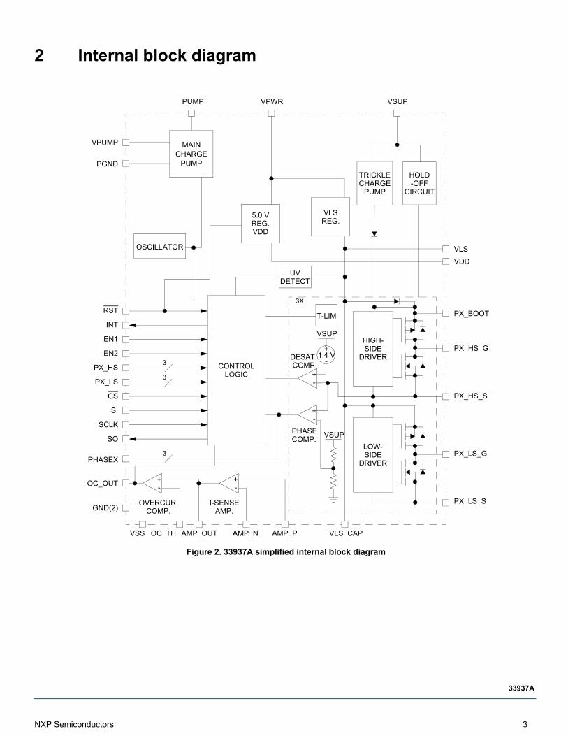
2 Internal block diagram
Figure 2. 33937A simplified internal block diagram
VPUMP
PUMP VSUPVPWR
VLS
VDD
PX_HS
PX_LS
PHASEX
CS
SI
SCLK
SO
RST
INT
AMP_PAMP_NAMP_OUT
PX_LS_S
MAINCHARGE
PUMPPGND
EN1
EN2
OC_OUT
GND(2)
PX_BOOT
PX_HS_G
PX_HS_S
PX_LS_G
OC_TH VLS_CAP
TRICKLECHARGE
PUMP
HOLD-OFF
CIRCUIT
OSCILLATOR
CONTROLLOGIC
5.0 VREG.VDD
VLSREG.
UVDETECT
T-LIM
+-
+-
+-
1.4 V+
-
VSUP
VSUP
+-
OVERCUR.COMP.
I-SENSEAMP.
HIGH-SIDE
DRIVER
LOW-SIDE
DRIVER
3
3
3
3X
DESAT.COMP
PHASECOMP.
VSS
NXP Semiconductors 3
33937A
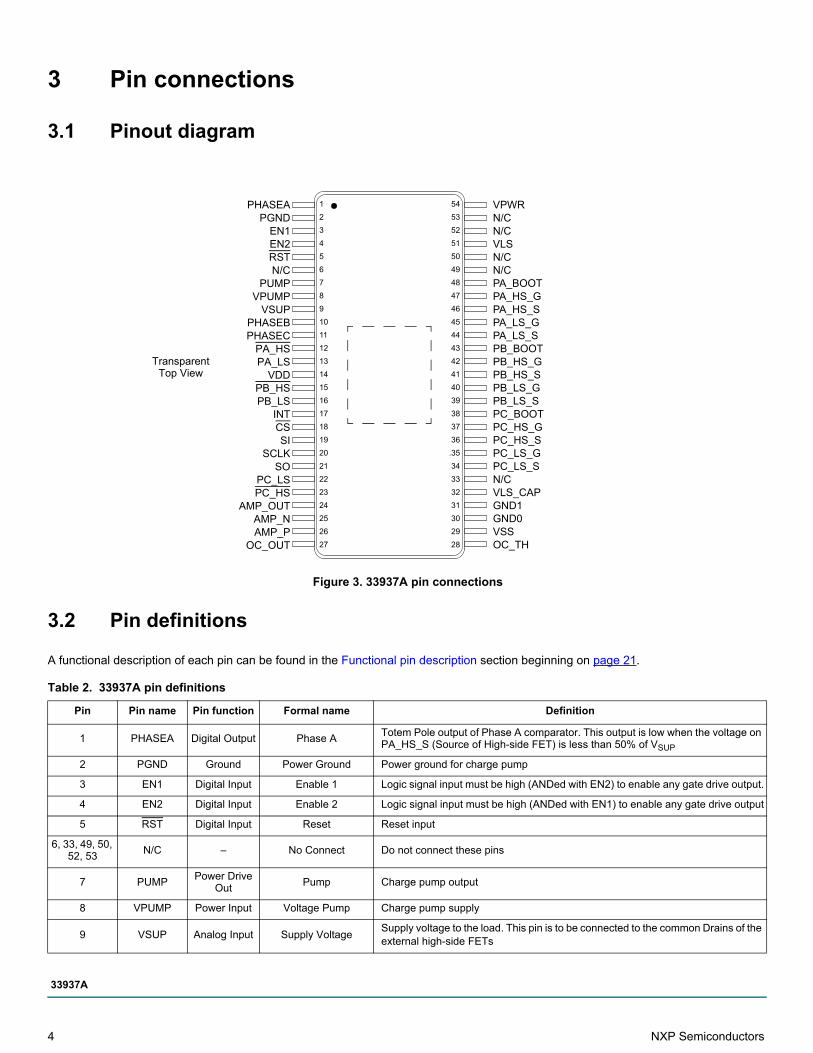
3 Pin connections
3.1 Pinout diagram
Figure 3. 33937A pin connections
3.2 Pin definitions
A functional description of each pin can be found in the Functional pin description section beginning on page 21. Table 2. 33937A pin definitions
Pin Pin name Pin function Formal name Definition
1 PHASEA Digital Output Phase ATotem Pole output of Phase A comparator. This output is low when the voltage on PA_HS_S (Source of High-side FET) is less than 50% of VSUP
2 PGND Ground Power Ground Power ground for charge pump
3 EN1 Digital Input Enable 1 Logic signal input must be high (ANDed with EN2) to enable any gate drive output.
4 EN2 Digital Input Enable 2 Logic signal input must be high (ANDed with EN1) to enable any gate drive output
5 RST Digital Input Reset Reset input
6, 33, 49, 50, 52, 53
N/C – No Connect Do not connect these pins
7 PUMPPower Drive
Out Pump Charge pump output
8 VPUMP Power Input Voltage Pump Charge pump supply
9 VSUP Analog Input Supply VoltageSupply voltage to the load. This pin is to be connected to the common Drains of the external high-side FETs
54
40
.35
34
33
32
31
30
29
28
39
38
37
36
47
46
45
44
43
42
41
51
50
49
48
53
52
1
15
20
21
22
23
24
25
26
27
16
17
18
19
8
9
10
11
12
13
14
4
5
6
7
2
3
PHASEAPGND
EN1EN2RSTN/C
PUMPVPUMP
VSUPPHASEBPHASEC
PA_HSPA_LS
VDDPB_HSPB_LS
INTCSSI
SCLKSO
PC_LSPC_HS
AMP_OUTAMP_NAMP_P
OC_OUT
VPWRN/CN/CVLSN/CN/CPA_BOOTPA_HS_GPA_HS_SPA_LS_GPA_LS_SPB_BOOTPB_HS_GPB_HS_SPB_LS_GPB_LS_SPC_BOOTPC_HS_GPC_HS_SPC_LS_GPC_LS_SN/CVLS_CAPGND1GND0VSSOC_TH
TransparentTop View
4 NXP Semiconductors
33937A
10 PHASEB Digital Output Phase BTotem Pole output of Phase B comparator. This output is low when the voltage on PB_HS_S (Source of high-side FET) is less than 50% of VSUP
11 PHASEC Digital Output Phase CTotem Pole output of Phase C comparator. This output is low when the voltage on PC_HS_S (Source of high-side FET) is less than 50% of VSUP
12 PA_HS Digital Input Phase A High-side Active low input logic signal enables the high-side driver for Phase A
13 PA_LS Digital Input Phase A Low-side Active high input logic signal enables the low-side driver for Phase A
14 VDDAnalog Output
VDD Regulator VDD regulator output capacitor connection.
15 PB_HS Digital Input Phase B High-side Active low input logic signal enables the high-side driver for Phase B
16 PB_LS Digital Input Phase B Low-side Active high input logic signal enables the low-side driver for Phase B
17 INT Digital Output Interrupt Interrupt pin output
18 CS Digital Input Chip Select Chip Select input. It frames SPI commands and enables SPI port
19 SI Digital Input Serial In Input data for SPI port. Clocked on the falling edge of SCLK, MSB first
20 SCLK Digital Input Serial Clock Clock for SPI port and typically is 3.0 MHz
21 SO Digital Output Serial Out Output data for SPI port. Tri-state until CS becomes low
22 PC_LS Digital Input Phase C Low-side Active high input logic signal enables the low-side driver for Phase C
23 PC_HS Digital Input Phase C High-side Active low input logic signal enables the high-side driver for Phase C
24 AMP_OUTAnalog Output
Amplifier Output Output of the current-sensing amplifier
25 AMP_N Analog Input Amplifier Invert Inverting input of the current-sensing amplifier
26 AMP_P Analog Input Amplifier Non-Invert Non-inverting input of the current-sensing amplifier
27 OC_OUT Digital Output Overcurrent Out Totem pole digital output of the overcurrent comparator
28 OC_TH Analog Input Overcurrent Threshold Threshold of the overcurrent detector
29 VSS Ground Voltage Source Supply Ground reference for logic interface and power supplies
30, 31 GND Ground Ground Substrate and ESD reference, connect to VSS
32 VLS_CAPAnalog Output
VLS Regulator Output Capacitor
VLS Regulator connection for additional output capacitor, providing low-impedance supply source for low-side gate drive
34 PC_LS_S Power InputPhase C Low-side
SourceSource connection for Phase C low-side FET
35 PC_LS_G Power OutputPhase C Low-side
Gate DriveGate drive output for Phase C low-side
36 PC_HS_S Power InputPhase C High-side
SourceSource connection for Phase C high-side FET
37 PC_HS_G Power OutputPhase C High-side
Gate DriveGate Drive for output Phase C high-side FET
38 PC_BOOT Analog Input Phase C Bootstrap Bootstrap capacitor for Phase C
39 PB_LS_S Power InputPhase B Low-side
SourceSource connection for Phase B low-side FET
40 PB_LS_G Power OutputPhase B Low-side
Gate DriveGate Drive for output Phase B low-side
41 PB_HS_S Power InputPhase B High-side
SourceSource connection for Phase B high-side FET
42 PB_HS_G Power OutputPhase B High-side
Gate DriveGate Drive for output Phase B high-side
43 PB_BOOT Analog Input Phase B Bootstrap Bootstrap capacitor for Phase B
44 PA_LS_S Power InputPhase A Low-side
SourceSource connection for Phase A low-side FET
Table 2. 33937A pin definitions (continued)
Pin Pin name Pin function Formal name Definition
NXP Semiconductors 5
33937A
45 PA_LS_G Power OutputPhase A Low-side
Gate DriveGate Drive for output Phase A low-side
46 PA_HS_S Power InputPhase A High-side
SourceSource connection for Phase A high-side FET
47 PA_HS_G Power OutputPhase A High-side
Gate DriveGate Drive for output Phase A high-side
48 PA_BOOT Analog Input Phase A Bootstrap Bootstrap capacitor for Phase A
51 VLSAnalog Output
VLS Regulator VLS regulator output. Power supply for the gate drives
54 VPWR Power Input Voltage Power Power supply input for gate drives
EP Ground Exposed PadDevice will perform as specified with the exposed pad un-terminated (floating) however, it is recommended that the exposed pad be terminated to pin 29 (VSS) and system ground
Table 2. 33937A pin definitions (continued)
Pin Pin name Pin function Formal name Definition
6 NXP Semiconductors
33937A
4 Electrical characteristics
4.1 Maximum ratings
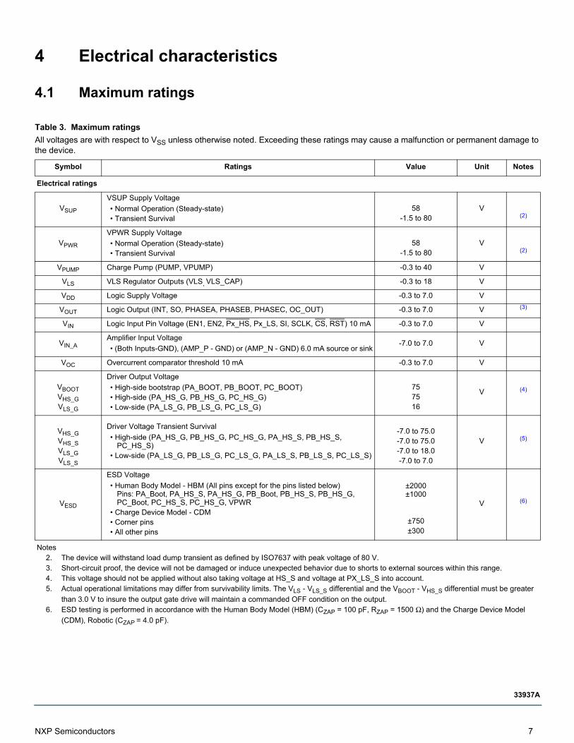
Table 3. Maximum ratings
All voltages are with respect to VSS unless otherwise noted. Exceeding these ratings may cause a malfunction or permanent damage to the device.
Symbol Ratings Value Unit Notes
Electrical ratings
VSUP
VSUP Supply Voltage
• Normal Operation (Steady-state)• Transient Survival
58 -1.5 to 80
V(2)
VPWR
VPWR Supply Voltage
• Normal Operation (Steady-state)• Transient Survival
58 -1.5 to 80
V(2)
VPUMP Charge Pump (PUMP, VPUMP) -0.3 to 40 V
VLS VLS Regulator Outputs (VLS, VLS_CAP) -0.3 to 18 V
VDD Logic Supply Voltage -0.3 to 7.0 V
VOUT Logic Output (INT, SO, PHASEA, PHASEB, PHASEC, OC_OUT) -0.3 to 7.0 V (3)
VIN Logic Input Pin Voltage (EN1, EN2, Px_HS, Px_LS, SI, SCLK, CS, RST) 10 mA -0.3 to 7.0 V
VIN_AAmplifier Input Voltage
• (Both Inputs-GND), (AMP_P - GND) or (AMP_N - GND) 6.0 mA source or sink-7.0 to 7.0 V
VOC Overcurrent comparator threshold 10 mA -0.3 to 7.0 V
VBOOTVHS_GVLS_G
Driver Output Voltage
• High-side bootstrap (PA_BOOT, PB_BOOT, PC_BOOT)• High-side (PA_HS_G, PB_HS_G, PC_HS_G)• Low-side (PA_LS_G, PB_LS_G, PC_LS_G)
757516
V (4)
VHS_GVHS_SVLS_GVLS_S
Driver Voltage Transient Survival
• High-side (PA_HS_G, PB_HS_G, PC_HS_G, PA_HS_S, PB_HS_S, PC_HS_S)
• Low-side (PA_LS_G, PB_LS_G, PC_LS_G, PA_LS_S, PB_LS_S, PC_LS_S)
-7.0 to 75.0-7.0 to 75.0-7.0 to 18.0-7.0 to 7.0
V (5)
VESD
ESD Voltage
• Human Body Model - HBM (All pins except for the pins listed below) Pins: PA_Boot, PA_HS_S, PA_HS_G, PB_Boot, PB_HS_S, PB_HS_G, PC_Boot, PC_HS_S, PC_HS_G, VPWR
• Charge Device Model - CDM• Corner pins• All other pins
±2000±1000
±750±300
V (6)
Notes2. The device will withstand load dump transient as defined by ISO7637 with peak voltage of 80 V.3. Short-circuit proof, the device will not be damaged or induce unexpected behavior due to shorts to external sources within this range.4. This voltage should not be applied without also taking voltage at HS_S and voltage at PX_LS_S into account. 5. Actual operational limitations may differ from survivability limits. The VLS - VLS_S differential and the VBOOT - VHS_S differential must be greater
than 3.0 V to insure the output gate drive will maintain a commanded OFF condition on the output.6. ESD testing is performed in accordance with the Human Body Model (HBM) (CZAP = 100 pF, RZAP = 1500 Ω) and the Charge Device Model
(CDM), Robotic (CZAP = 4.0 pF).
NXP Semiconductors 7
33937A
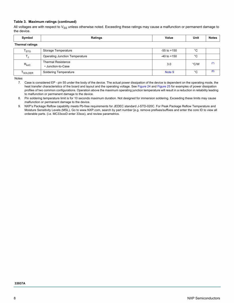
Thermal ratings
TSTG Storage Temperature -55 to +150 °C
TJ Operating Junction Temperature -40 to +150 °C
RθJCThermal Resistance
• Junction-to-Case3.0 °C/W (7)
TSOLDER Soldering Temperature Note 9 °C (8)
Notes7. Case is considered EP - pin 55 under the body of the device. The actual power dissipation of the device is dependent on the operating mode, the
heat transfer characteristics of the board and layout and the operating voltage. See Figure 24 and Figure 25 for examples of power dissipation profiles of two common configurations. Operation above the maximum operating junction temperature will result in a reduction in reliability leading to malfunction or permanent damage to the device.
8. Pin soldering temperature limit is for 10 seconds maximum duration. Not designed for immersion soldering. Exceeding these limits may cause malfunction or permanent damage to the device.
9. NXP’s Package Reflow capability meets Pb-free requirements for JEDEC standard J-STD-020C. For Peak Package Reflow Temperature and Moisture Sensitivity Levels (MSL), Go to www.NXP.com, search by part number [e.g. remove prefixes/suffixes and enter the core ID to view all orderable parts. (i.e. MC33xxxD enter 33xxx), and review parametrics.
Table 3. Maximum ratings (continued)
All voltages are with respect to VSS unless otherwise noted. Exceeding these ratings may cause a malfunction or permanent damage to the device.
Symbol Ratings Value Unit Notes
8 NXP Semiconductors
33937A
4.2 Static electrical characteristics
Table 4. Static electrical characteristics
Characteristics noted under conditions 8.0 V ≤ VPWR = VSUP ≤ 40 V, - 40 °C ≤ TA ≤ 135 °C, unless otherwise noted. Typical values noted reflect the approximate parameter means at TA = 25 °C under nominal conditions, unless otherwise noted.
Symbol Characteristic Min. Typ. Max. Unit Notes
Power inputs
VPWR_ST VPWR Supply Voltage Startup Threshold – 6.0 8.0 V (10)
ISUP
VSUP Supply Current, VPWR = VSUP = 40 V, RST and ENABLE = 5.0 V
• No output loads on Gate Drive Pins, No PWM• No output loads on Gate Drive Pins, 20 kHz, 50% Duty Cycle
––
1.0–
–10
mA
IPWR_ON
VPWR Supply Current, VPWR = VSUP = 40 V, RST and ENABLE = 5.0 V
• No output loads on Gate Drive Pins, No PWM, Outputs initialized
• Output Loads = 620 nC per FET, 20 kHz PWM
––
11–
2095
mA
(11)
ISUPIPWR
Sleep State Supply Current, RST = 0 V
• VSUP = 40 V
• VPWR = 40 V––
1456
30100
µA
VGATESSSleep State Output Gate Voltage
• IG < 100 µA– – 1.3 V
VBootTrickle Charge Pump (Bootstrap Voltage)
• VSUP = 14 V22 28 32 V (15)
VF Bootstrap Diode Forward Voltage at 10 mA – – 1.2 V
VDD internal regulator
VDDVDD Output Voltage, VPWR = 8 to 40 V, C = 0.47 µF
• External Load IDD_EXT = 0 to 1.0 mA 4.5 – 5.5 V (12)
IDD Internal VDD Supply Current, VDD = 5.5 V, No External Load – – 12 mA
VLS regulator
IPEAK Peak Output Current, VPWR = 16 V, VLS = 10 V 350 600 800 mA
VLSLinear Regulator Output Voltage, IVLS = 0 to 60 mA, VPWR > VLS + 2.0 V
13.5 15 17 V (13)
VTHVLS VLS Disable Threshold 7.5 8.0 8.5 V (14)
Notes10. Operation with the Charge Pump is recommended when minimum system voltage could be less than 14 V. VPWR must exceed this threshold in
order for the Charge Pump and VDD regulator to startup and drive VPWR to > 8.0 V. Once VPWR exceeds 8.0 V, the circuits will continue to operate
even if system voltage drops below 6.0 V.11. This parameter is guaranteed by design. It is not production tested.12. Minimum external capacitor for stable VDD operation is 0.47 µF.
13. Recommended external capacitor for the VLS regulator is 2.2 µF low ESR at each pin VLS and VLS_CAP.
14. When VLS is less than this value, the outputs are disabled and HOLDOFF circuits are active. Recovery requires initialization when VLS rises above
this threshold again. A filter delay of approximately 700 ns on the comparator output eliminates responses to spurious transients on VLS.
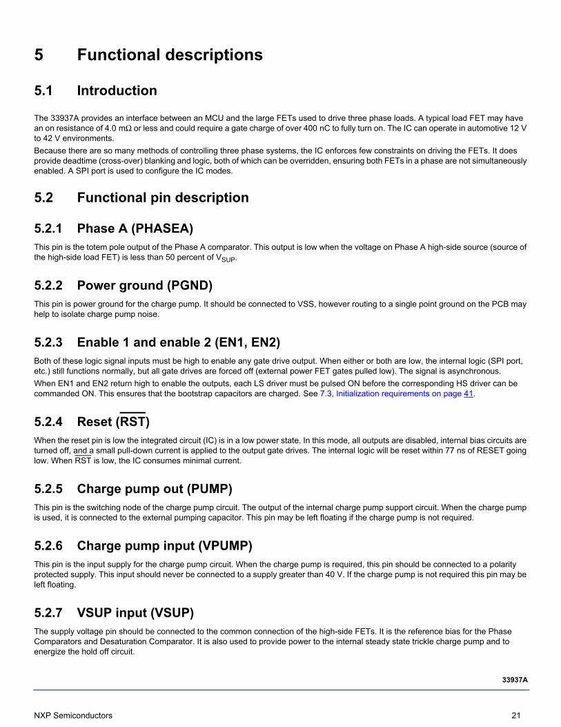
15. See Figure 11 for typical capability to maintain gate voltage with a 5.0 µA load.
NXP Semiconductors 9
33937A
Charge pump
RDS(on)_HSRDS(on)_LS
VTHREG
Charge Pump
• High-side Switch On Resistance• Low-side Switch On Resistance• Regulation Threshold Difference
––
250
6.05.0500
109.4900
ΩΩ
mV (16), (18)
VCP
Charge Pump Output Voltage
• IOUT = 40 mA, 6.0 V < VSYS < 8.0 V
• IOUT = 40 mA, VSYS > = 8.0 V 8.512
9.5–
––
V (17), (18)
Gate drive
RDS(on)_H_SRC
High-side Driver On Resistance (Sourcing)
• VPWR = VSUP = 16 V, - 40 °C ≤ TA ≤ 25 °C• VPWR = VSUP = 16 V, 25 °C < TA ≤ 135 °C
––
––
6.08.5
Ω
RDS(on)_H_SINKHigh-side Driver On Resistance (Sinking)
• VPWR = VSUP = 16 V– – 3.0 Ω
IHS_INJ High-side Current Injection Allowed Without Malfunction – – 0.5 A (18), (19)
RDS(on)_L_SRC
Low-side Driver On Resistance (Sourcing)
• VPWR = VSUP = 16 V, - 40 °C ≤ TA ≤ 25 °C• VPWR = VSUP = 16 V, 25 °C < TA ≤ 135 °C
––
––
6.08.5
Ω
RDS(on)_L_SINKLow-side Driver On-Resistance (Sinking)
• VPWR = VSUP = 16 V– – 3.0 Ω
ILS_INJ Low-side Current Injection Allowed Without Malfunction – – 0.5 Α (18), (19)
VGS_HVGS_L
Gate Source Voltage, VPWR = VSUP = 40 V
• High-side, IGATE = 0
• Low-side, IGATE = 01313
14.815.4
16.517
V (20)
VHS_G_HOLD
Reverse High-side Gate Holding Voltage
Gate Output Holding Current = 2.0 µA
Gate Output Holding Current = 5.0 µA, VSUP<26 V
Gate Output Holding Current = 5.0 µA, VSUP<40 V
–––
1010–
151515
V (21)
Notes16. When VLS is this amount below the normal VLS linear regulation threshold, the charge pump is enabled. 17. VSYS is the system voltage on the input to the charge pump. Recommended external components: 1.0 µF MLC, MUR 120 diode.
18. This parameter is a design characteristic, not production tested.19. Current injection only occurs during output switch transitions. The IC is immune to specified injected currents for a duration of approximately 1.0 µs
after an output switch transition. 1.0 µs is sufficient for all intended applications of this IC.20. If a slightly higher gate voltage is required, larger bootstrap capacitors are required. At high duty cycles, the bootstrap voltage may not recover
completely, leading to a higher output on-resistance. This effect can be minimized by using low ESR capacitors for the bootstrap and the VLS capacitors.
21. High-side Gate Holding voltage is the voltage between the Gate and Source of the high-side FET when held in an on condition. The trickle charge pump supplies bias and holding current for the High-side FET gate driver and output to maintain voltages after bootstrap events. See Figure 11 for typical 100% high-side gate voltage with a 5.0 µA load. This parameter is a design characteristic, not production tested.
Table 4. Static electrical characteristics (continued)
Characteristics noted under conditions 8.0 V ≤ VPWR = VSUP ≤ 40 V, - 40 °C ≤ TA ≤ 135 °C, unless otherwise noted. Typical values noted reflect the approximate parameter means at TA = 25 °C under nominal conditions, unless otherwise noted.
Symbol Characteristic Min. Typ. Max. Unit Notes
10 NXP Semiconductors
33937A
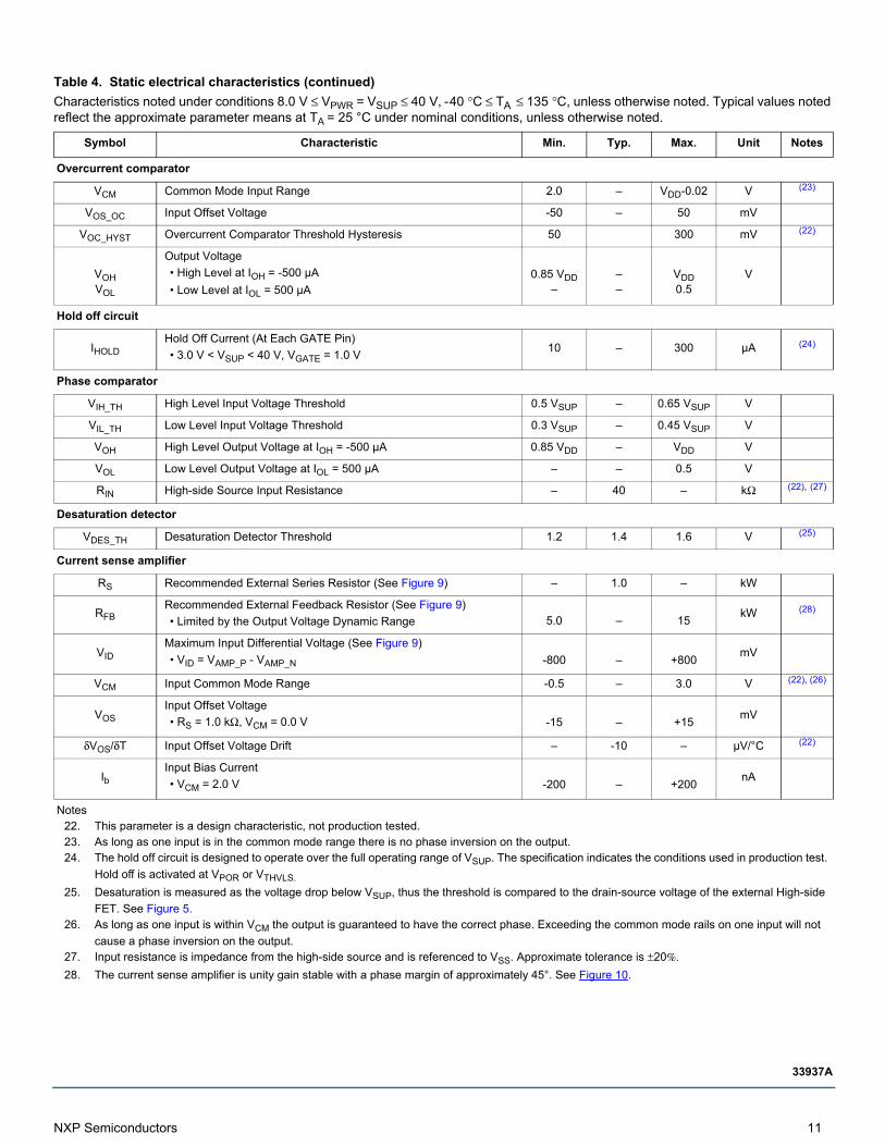
Overcurrent comparator
VCM Common Mode Input Range 2.0 – VDD-0.02 V (23)
VOS_OC Input Offset Voltage -50 – 50 mV
VOC_HYST Overcurrent Comparator Threshold Hysteresis 50 300 mV (22)
VOHVOL
Output Voltage
• High Level at IOH = -500 µA
• Low Level at IOL = 500 µA0.85 VDD
–––
VDD0.5
V
Hold off circuit
IHOLDHold Off Current (At Each GATE Pin)
• 3.0 V < VSUP < 40 V, VGATE = 1.0 V10 – 300 µA (24)
Phase comparator
VIH_TH High Level Input Voltage Threshold 0.5 VSUP – 0.65 VSUP V
VIL_TH Low Level Input Voltage Threshold 0.3 VSUP – 0.45 VSUP V
VOH High Level Output Voltage at IOH = -500 µA 0.85 VDD – VDD V
VOL Low Level Output Voltage at IOL = 500 µA – – 0.5 V
RIN High-side Source Input Resistance – 40 – kΩ (22), (27)
Desaturation detector
VDES_TH Desaturation Detector Threshold 1.2 1.4 1.6 V (25)
Current sense amplifier
RS Recommended External Series Resistor (See Figure 9) – 1.0 – kW
RFBRecommended External Feedback Resistor (See Figure 9)
• Limited by the Output Voltage Dynamic Range 5.0 – 15kW (28)
VIDMaximum Input Differential Voltage (See Figure 9)
• VID = VAMP_P - VAMP_N -800 – +800mV
VCM Input Common Mode Range -0.5 – 3.0 V (22), (26)
VOSInput Offset Voltage
• RS = 1.0 kΩ, VCM = 0.0 V -15 – +15mV
δVOS/δT Input Offset Voltage Drift – -10 – µV/°C (22)
IbInput Bias Current
• VCM = 2.0 V -200 – +200nA
Notes22. This parameter is a design characteristic, not production tested.23. As long as one input is in the common mode range there is no phase inversion on the output.24. The hold off circuit is designed to operate over the full operating range of VSUP. The specification indicates the conditions used in production test.
Hold off is activated at VPOR or VTHVLS.
25. Desaturation is measured as the voltage drop below VSUP, thus the threshold is compared to the drain-source voltage of the external High-side
FET. See Figure 5.26. As long as one input is within VCM the output is guaranteed to have the correct phase. Exceeding the common mode rails on one input will not
cause a phase inversion on the output.27. Input resistance is impedance from the high-side source and is referenced to VSS. Approximate tolerance is ±20%.28. The current sense amplifier is unity gain stable with a phase margin of approximately 45°. See Figure 10.
Table 4. Static electrical characteristics (continued)
Characteristics noted under conditions 8.0 V ≤ VPWR = VSUP ≤ 40 V, - 40 °C ≤ TA ≤ 135 °C, unless otherwise noted. Typical values noted reflect the approximate parameter means at TA = 25 °C under nominal conditions, unless otherwise noted.
Symbol Characteristic Min. Typ. Max. Unit Notes
NXP Semiconductors 11
33937A
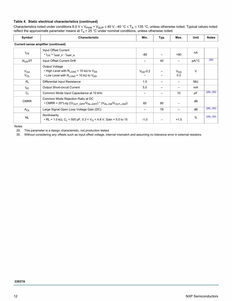
Current sense amplifier (continued)
IOSInput Offset Current
• IOS = IAMP_P - IAMP_N -80 – +80nA
δIOS/δT Input Offset Current Drift – 40 – pA/°C (29)
VOHVOL
Output Voltage
• High Level with RLOAD = 10 kΩ to VSS
• Low Level with RLOAD = 10 kΩ to VDD
VDD-0.2–
––
VDD0.2
V
RI Differential Input Resistance 1.0 – – MΩ
ISC Output Short-circuit Current 5.0 – – mA
CI Common Mode Input Capacitance at 10 kHz – – 10 pF (29), (30)
CMRRCommon Mode Rejection Ratio at DC
• CMRR = 20*Log ((VOUT_DIFF/VIN_DIFF) * (VIN_CM/VOUT_CM)) 60 80 –dB
AOL Large Signal Open Loop Voltage Gain (DC) – 78 – dB (29), (30)
NLNonlinearity
• RL = 1.0 kΩ, CL = 500 pF, 0.3 < VO < 4.8 V, Gain = 5.0 to 15 -1.0 – +1.0% (29), (30)
Notes29. This parameter is a design characteristic, not production tested.30. Without considering any offsets such as input offset voltage, internal mismatch and assuming no tolerance error in external resistors.
Table 4. Static electrical characteristics (continued)
Characteristics noted under conditions 8.0 V ≤ VPWR = VSUP ≤ 40 V, - 40 °C ≤ TA ≤ 135 °C, unless otherwise noted. Typical values noted reflect the approximate parameter means at TA = 25 °C under nominal conditions, unless otherwise noted.
Symbol Characteristic Min. Typ. Max. Unit Notes
12 NXP Semiconductors
33937A
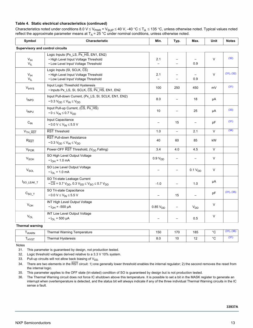
Supervisory and control circuits
VIHVIL
Logic Inputs (Px_LS, Px_HS, EN1, EN2)
• High Level Input Voltage Threshold• Low Level Input Voltage Threshold
2.1–
––
–0.9
V (32)
VIHVIL
Logic Inputs (SI, SCLK, CS)
• High Level Input Voltage Threshold• Low Level Input Voltage Threshold
2.1–
––
–0.9
V (31), (32)
VIHYSInput Logic Threshold Hysteresis
• Inputs Px_LS, SI, SCLK, CS, Px_HS, EN1, EN2100 250 450 mV (31)
IINPDInput Pull-down Current, (Px_LS, SI, SCLK, EN1, EN2)
• 0.3 VDD ≤ VIN ≤ VDD 8.0 – 18 µA
IINPUInput Pull-up Current, (CS, Px_HS)
• 0 ≤ VIN ≤ 0.7 VDD10 – 25 µA (33)
CINInput Capacitance
• 0.0 V ≤ VIN ≤ 5.5 V – 15 – pF (31)
VTH_RST RST Threshold 1.0 – 2.1 V (34)
RRSTRST Pull-down Resistance
• 0.3 VDD ≤ VIN ≤ VDD40 60 85 kW
VPOR Power-OFF RST Threshold, (VDD Falling) 3.4 4.0 4.5 V
VSOHSO High Level Output Voltage
• IOH = 1.0 mA0.9 VDD – – V
VSOLSO Low Level Output Voltage
• IOL = 1.0 mA– – 0.1 VDD V
ISO_LEAK_TSO Tri-state Leakage Current
• CS = 0.7 VDD, 0.3 VDD ≤ VSO ≤ 0.7 VDD -1.0 – 1.0µA
CSO_TSO Tri-state Capacitance
• 0.0 V ≤ VIN ≤ 5.5 V – 15 –pF (31), (35)
VOHINT High Level Output Voltage
• IOH = -500 µA 0.85 VDD – VDDV
VOLINT Low Level Output Voltage
• IOL = 500 µA – – 0.5V
Thermal warning
TWARN Thermal Warning Temperature 150 170 185 °C (31), (36)
THYST Thermal Hysteresis 8.0 10 12 °C (31)
Notes31. This parameter is guaranteed by design, not production tested.32. Logic threshold voltages derived relative to a 3.3 V 10% system.33. Pull-up circuits will not allow back biasing of VDD.
34. There are two elements in the RST circuit: 1) one generally lower threshold enables the internal regulator; 2) the second removes the reset from the internal logic.
35. This parameter applies to the OFF state (tri-stated) condition of SO is guaranteed by design but is not production tested.36. The Thermal Warning circuit does not force IC shutdown above this temperature. It is possible to set a bit in the MASK register to generate an
interrupt when overtemperature is detected, and the status bit will always indicate if any of the three individual Thermal Warning circuits in the IC sense a fault.
Table 4. Static electrical characteristics (continued)
Characteristics noted under conditions 8.0 V ≤ VPWR = VSUP ≤ 40 V, - 40 °C ≤ TA ≤ 135 °C, unless otherwise noted. Typical values noted reflect the approximate parameter means at TA = 25 °C under nominal conditions, unless otherwise noted.
Symbol Characteristic Min. Typ. Max. Unit Notes
NXP Semiconductors 13
33937A
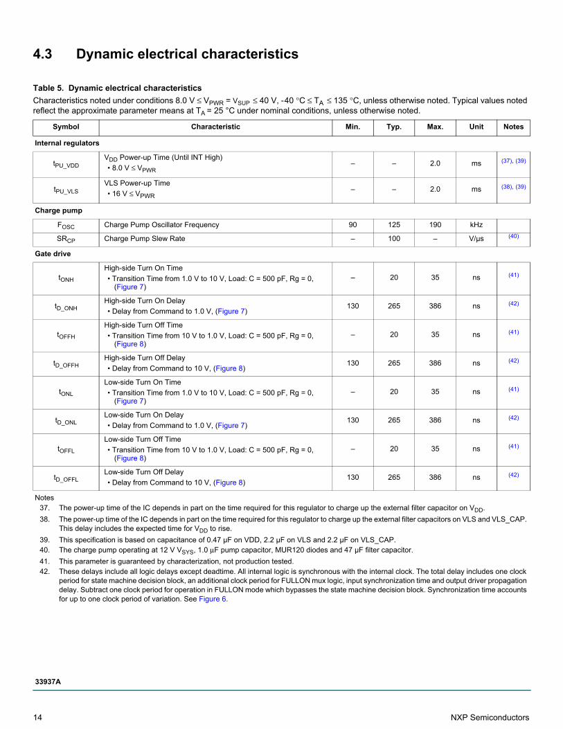
4.3 Dynamic electrical characteristics
Table 5. Dynamic electrical characteristics
Characteristics noted under conditions 8.0 V ≤ VPWR = VSUP ≤ 40 V, - 40 °C ≤ TA ≤ 135 °C, unless otherwise noted. Typical values noted reflect the approximate parameter means at TA = 25 °C under nominal conditions, unless otherwise noted.
Symbol Characteristic Min. Typ. Max. Unit Notes
Internal regulators
tPU_VDDVDD Power-up Time (Until INT High)
• 8.0 V ≤ VPWR – – 2.0 ms (37), (39)
tPU_VLSVLS Power-up Time
• 16 V ≤ VPWR – – 2.0 ms (38), (39)
Charge pump
FOSC Charge Pump Oscillator Frequency 90 125 190 kHz
SRCP Charge Pump Slew Rate – 100 – V/µs (40)
Gate drive
tONH
High-side Turn On Time
• Transition Time from 1.0 V to 10 V, Load: C = 500 pF, Rg = 0, (Figure 7)
– 20 35 ns (41)
tD_ONHHigh-side Turn On Delay
• Delay from Command to 1.0 V, (Figure 7)130 265 386 ns (42)
tOFFH
High-side Turn Off Time
• Transition Time from 10 V to 1.0 V, Load: C = 500 pF, Rg = 0, (Figure 8)
– 20 35 ns (41)
tD_OFFHHigh-side Turn Off Delay
• Delay from Command to 10 V, (Figure 8)130 265 386 ns (42)
tONL
Low-side Turn On Time
• Transition Time from 1.0 V to 10 V, Load: C = 500 pF, Rg = 0, (Figure 7)
– 20 35 ns (41)
tD_ONLLow-side Turn On Delay
• Delay from Command to 1.0 V, (Figure 7)130 265 386 ns (42)
tOFFL
Low-side Turn Off Time
• Transition Time from 10 V to 1.0 V, Load: C = 500 pF, Rg = 0, (Figure 8)
– 20 35 ns (41)
tD_OFFLLow-side Turn Off Delay
• Delay from Command to 10 V, (Figure 8)130 265 386 ns (42)
Notes37. The power-up time of the IC depends in part on the time required for this regulator to charge up the external filter capacitor on VDD.
38. The power-up time of the IC depends in part on the time required for this regulator to charge up the external filter capacitors on VLS and VLS_CAP. This delay includes the expected time for VDD to rise.
39. This specification is based on capacitance of 0.47 µF on VDD, 2.2 µF on VLS and 2.2 µF on VLS_CAP.40. The charge pump operating at 12 V VSYS, 1.0 μF pump capacitor, MUR120 diodes and 47 µF filter capacitor.
41. This parameter is guaranteed by characterization, not production tested.42. These delays include all logic delays except deadtime. All internal logic is synchronous with the internal clock. The total delay includes one clock
period for state machine decision block, an additional clock period for FULLON mux logic, input synchronization time and output driver propagation delay. Subtract one clock period for operation in FULLON mode which bypasses the state machine decision block. Synchronization time accounts for up to one clock period of variation. See Figure 6.
14 NXP Semiconductors
33937A
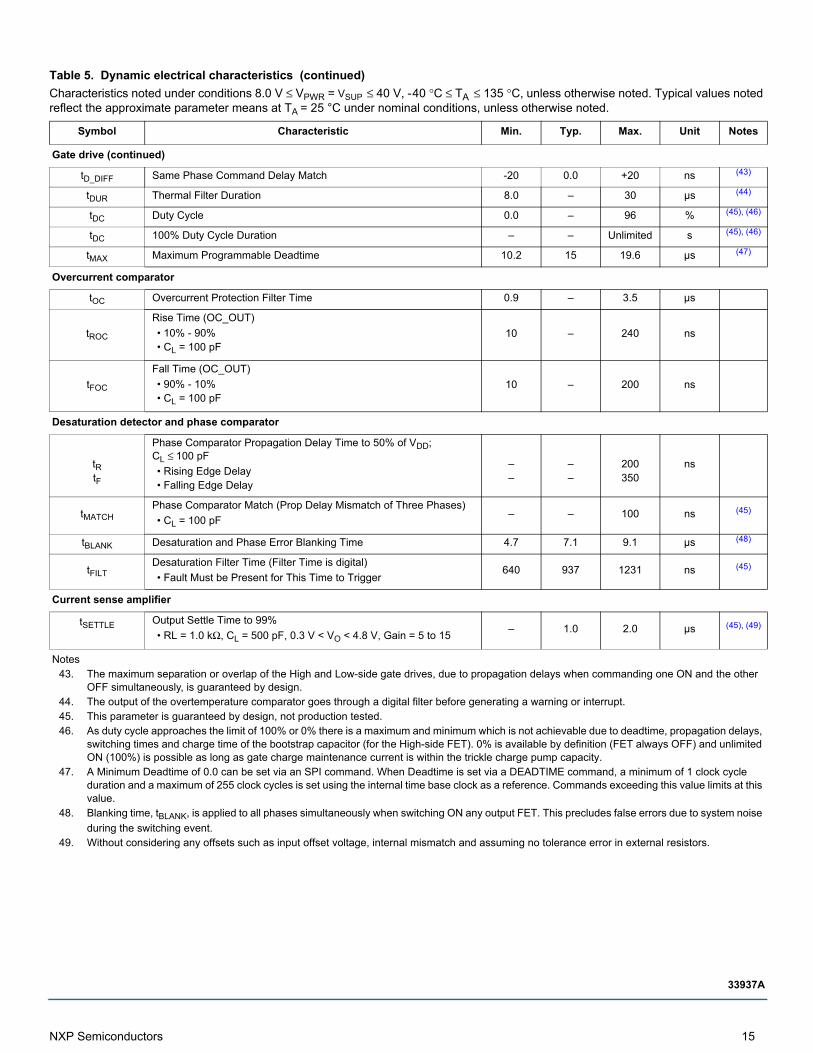
Gate drive (continued)
tD_DIFF Same Phase Command Delay Match -20 0.0 +20 ns (43)
tDUR Thermal Filter Duration 8.0 – 30 µs (44)
tDC Duty Cycle 0.0 – 96 % (45), (46)
tDC 100% Duty Cycle Duration – – Unlimited s (45), (46)
tMAX Maximum Programmable Deadtime 10.2 15 19.6 µs (47)
Overcurrent comparator
tOC Overcurrent Protection Filter Time 0.9 – 3.5 µs
tROC
Rise Time (OC_OUT)
• 10% - 90%• CL = 100 pF
10 – 240 ns
tFOC
Fall Time (OC_OUT)
• 90% - 10%• CL = 100 pF
10 – 200 ns
Desaturation detector and phase comparator
tRtF
Phase Comparator Propagation Delay Time to 50% of VDD; CL ≤ 100 pF
• Rising Edge Delay• Falling Edge Delay
––
––
200350
ns
tMATCHPhase Comparator Match (Prop Delay Mismatch of Three Phases)
• CL = 100 pF – – 100 ns (45)
tBLANK Desaturation and Phase Error Blanking Time 4.7 7.1 9.1 µs (48)
tFILTDesaturation Filter Time (Filter Time is digital)
• Fault Must be Present for This Time to Trigger640 937 1231 ns (45)
Current sense amplifier
tSETTLE Output Settle Time to 99%
• RL = 1.0 kΩ, CL = 500 pF, 0.3 V < VO < 4.8 V, Gain = 5 to 15– 1.0 2.0 µs (45), (49)
Notes43. The maximum separation or overlap of the High and Low-side gate drives, due to propagation delays when commanding one ON and the other
OFF simultaneously, is guaranteed by design.44. The output of the overtemperature comparator goes through a digital filter before generating a warning or interrupt.45. This parameter is guaranteed by design, not production tested.46. As duty cycle approaches the limit of 100% or 0% there is a maximum and minimum which is not achievable due to deadtime, propagation delays,
switching times and charge time of the bootstrap capacitor (for the High-side FET). 0% is available by definition (FET always OFF) and unlimited ON (100%) is possible as long as gate charge maintenance current is within the trickle charge pump capacity.
47. A Minimum Deadtime of 0.0 can be set via an SPI command. When Deadtime is set via a DEADTIME command, a minimum of 1 clock cycle duration and a maximum of 255 clock cycles is set using the internal time base clock as a reference. Commands exceeding this value limits at this value.
48. Blanking time, tBLANK, is applied to all phases simultaneously when switching ON any output FET. This precludes false errors due to system noise
during the switching event.49. Without considering any offsets such as input offset voltage, internal mismatch and assuming no tolerance error in external resistors.
Table 5. Dynamic electrical characteristics (continued)
Characteristics noted under conditions 8.0 V ≤ VPWR = VSUP ≤ 40 V, - 40 °C ≤ TA ≤ 135 °C, unless otherwise noted. Typical values noted reflect the approximate parameter means at TA = 25 °C under nominal conditions, unless otherwise noted.
Symbol Characteristic Min. Typ. Max. Unit Notes
NXP Semiconductors 15
33937A

Current sense amplifier (continued)
tIS_RISEOutput Rise Time to 90%
• RL = 1.0 kΩ, CL = 500 pF, 0.3 V < VO < 4.8 V, Gain = 5.0 to 15– – 1.0 µs (51)
tIS_FALLOutput Fall Time to 10%
• RL = 1.0 kΩ, CL = 500 pF, 0.3 V < VO < 4.8 V, Gain = 5.0 to 15– – 1.0 µs (51)
SR(5) Slew Rate at Gain = 5.0
• RL = 1.0 kΩ, CL = 20 pF 5.0 – – V/µs (50)
fM Phase Margin at Gain = 5.0 – 30 – ° (50)
GBWUnity Gain Bandwidth
• RL = 1.0 kΩ, CL = 100 pF – 20 – MHz (50)
BWGBandwidth at Gain = 15
• RL = 1.0 kΩ, CL = 50 pF 2.0 – –MHz (50)
CMR
Common Mode Rejection (CMR) with VIN
• VIN_CM = 400 mV*sin(2*π*freq*t)
• VIN_DIF = 0.0 V, RS = 1.0 kΩ• RFB = 15 kΩ, VREFIN = 0.0 V
CMR = 20*Log(VOUT/VIN_CM)
• Freq = 100 kHz• Freq = 1.0 MHz• Freq = 10 MHz
504030
–––
–––
dB (50)
Supervisory and control circuits
tPROP EN1 and EN2 Propagation Delay – – 280 ns
tRINT INT Rise Time CL = 100 pF 10 – 250 ns
tFINT INT Fall Time CL = 100 pF 10 – 200 ns
tPROPINT INT Propagation Time – – 250 ns
tTRRST RST Transition Time (Rise and Fall) – – 1.25 µs (50),(52)
Notes50. This parameter is guaranteed by design, not production tested.51. Rise and fall times are measured from the transition of a step function on the input to 90% of the change in output voltage.
52. tTRRST is given as a design guideline. The bounds for this specification are VPWR ≤ 58 V, total capacitance on VLS > 1.0 µF.
Table 5. Dynamic electrical characteristics (continued)
Characteristics noted under conditions 8.0 V ≤ VPWR = VSUP ≤ 40 V, - 40 °C ≤ TA ≤ 135 °C, unless otherwise noted. Typical values noted reflect the approximate parameter means at TA = 25 °C under nominal conditions, unless otherwise noted.
Symbol Characteristic Min. Typ. Max. Unit Notes
16 NXP Semiconductors
33937A
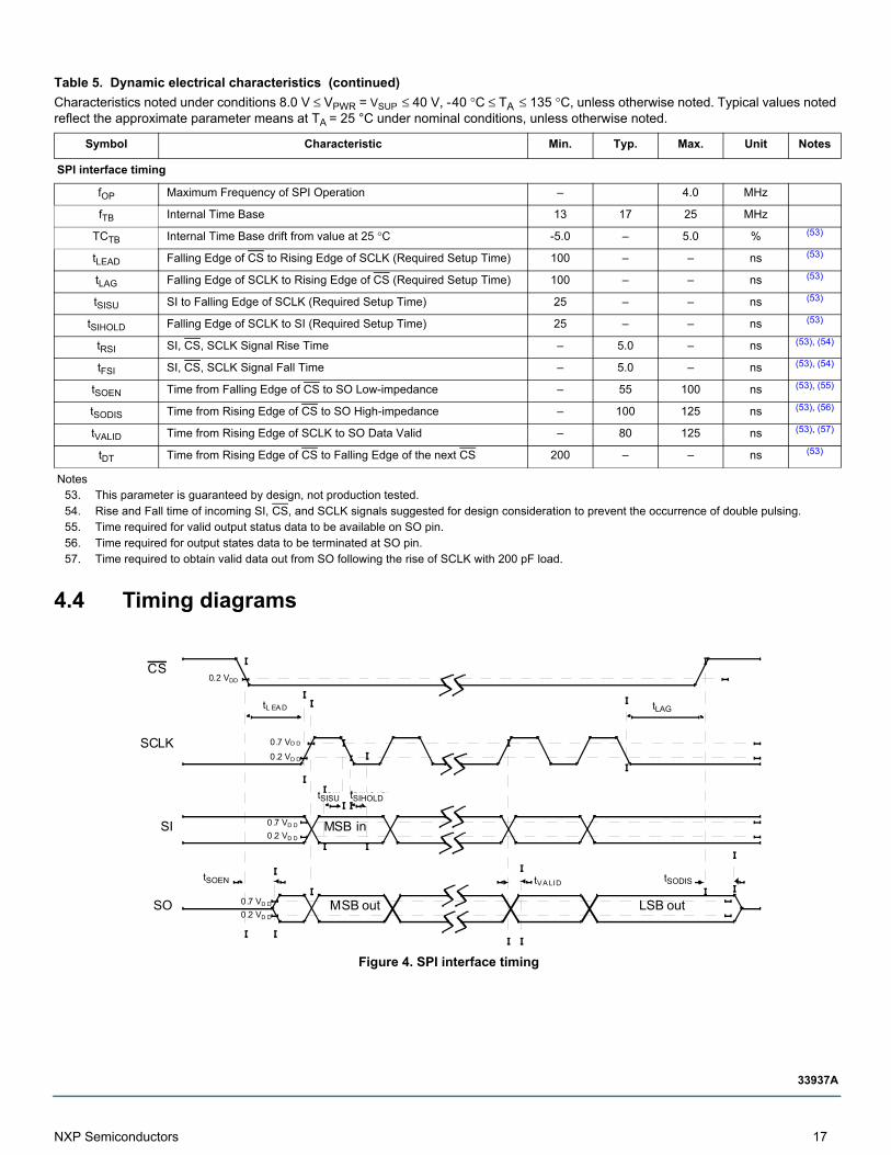
4.4 Timing diagrams
Figure 4. SPI interface timing
SPI interface timing
fOP Maximum Frequency of SPI Operation – 4.0 MHz
fTB Internal Time Base 13 17 25 MHz
TCTB Internal Time Base drift from value at 25 °C -5.0 – 5.0 % (53)
tLEAD Falling Edge of CS to Rising Edge of SCLK (Required Setup Time) 100 – – ns (53)
tLAG Falling Edge of SCLK to Rising Edge of CS (Required Setup Time) 100 – – ns (53)
tSISU SI to Falling Edge of SCLK (Required Setup Time) 25 – – ns (53)
tSIHOLD Falling Edge of SCLK to SI (Required Setup Time) 25 – – ns (53)
tRSI SI, CS, SCLK Signal Rise Time – 5.0 – ns (53), (54)
tFSI SI, CS, SCLK Signal Fall Time – 5.0 – ns (53), (54)
tSOEN Time from Falling Edge of CS to SO Low-impedance – 55 100 ns (53), (55)
tSODIS Time from Rising Edge of CS to SO High-impedance – 100 125 ns (53), (56)
tVALID Time from Rising Edge of SCLK to SO Data Valid – 80 125 ns (53), (57)
tDT Time from Rising Edge of CS to Falling Edge of the next CS 200 – – ns (53)
Notes53. This parameter is guaranteed by design, not production tested.54. Rise and Fall time of incoming SI, CS, and SCLK signals suggested for design consideration to prevent the occurrence of double pulsing.55. Time required for valid output status data to be available on SO pin.56. Time required for output states data to be terminated at SO pin.57. Time required to obtain valid data out from SO following the rise of SCLK with 200 pF load.
Table 5. Dynamic electrical characteristics (continued)
Characteristics noted under conditions 8.0 V ≤ VPWR = VSUP ≤ 40 V, - 40 °C ≤ TA ≤ 135 °C, unless otherwise noted. Typical values noted reflect the approximate parameter means at TA = 25 °C under nominal conditions, unless otherwise noted.
Symbol Characteristic Min. Typ. Max. Unit Notes
tDO (DIS )
0 .7 VD D
0.2 VDD
0.2 VD D
0.7 VD D
0.2 VD D
tL EAD
tDI(SU) tDI(HO LD)
tVALID
tLAG
CS
SCLK
SI
SO
MSB in
MSB out LSB out0.7 VD D
0.2 VD D
tDO(EN)tSODIStSOEN
tSISU tSIHOLD
tLAG
NXP Semiconductors 17
33937A
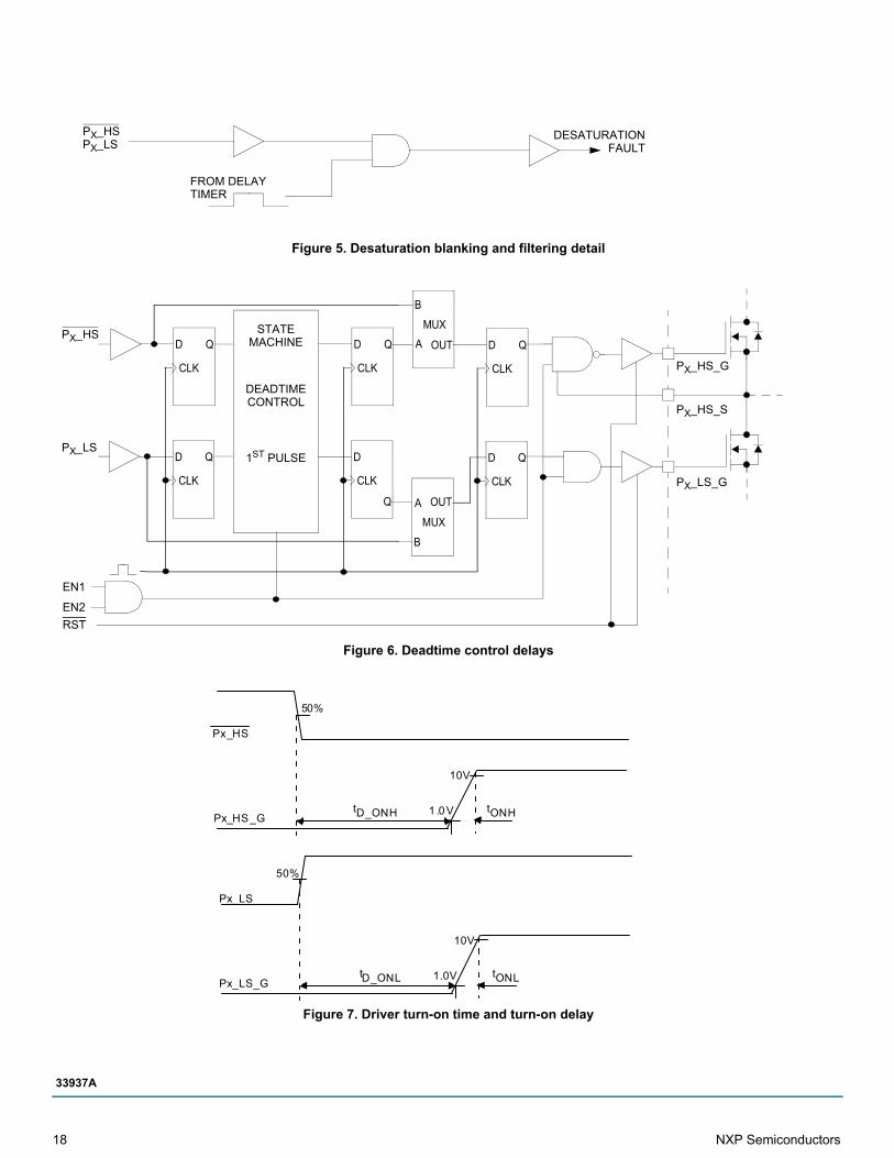
Figure 5. Desaturation blanking and filtering detail
Figure 6. Deadtime control delays
Figure 7. Driver turn-on time and turn-on delay
FROM DELAYTIMER
PX_HSPX_LS
DESATURATIONFAULT
PX_LS
PX_HS
EN1
EN2
RST
STATE
DEADTIMECONTROL
1ST PULSE
MACHINE
PX_HS_G
PX_HS_S
PX_LS_G
D Q
CLK
D
Q
CLK
D Q
CLK
D Q
CLK
D Q
CLK
D Q
CLK
B
OUTA
MUX
B
OUTA
MUX
50%
Px_HS_G
Px_HS
10V
1 .0 VtD_ONH tONH
50%
Px_LS_G
Px_LS
10V
1.0VtD_ONL tONL
18 NXP Semiconductors
33937A
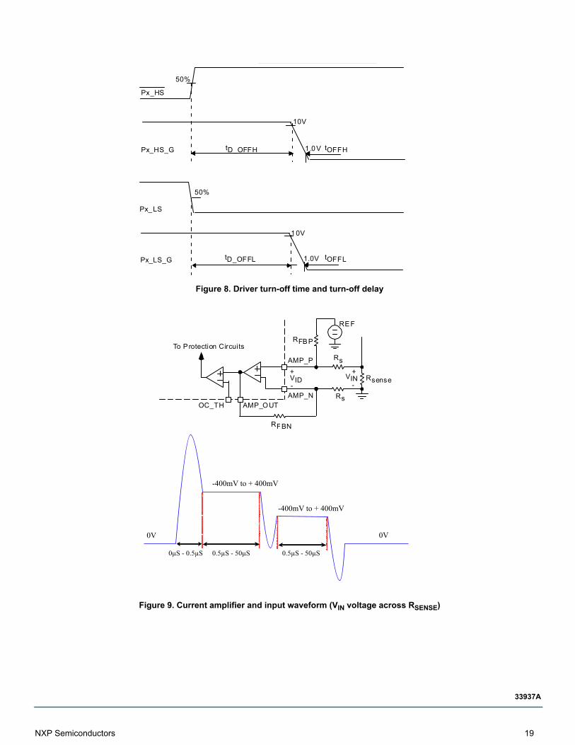
Figure 8. Driver turn-off time and turn-off delay
Figure 9. Current amplifier and input waveform (VIN voltage across RSENSE)
50%
10V
1.0VtD_OFFL tOFFLPx_LS_G
Px_LS
Px_HS_G
Px_HS
50%
10V
1 .0VtD_OFFH tOFFH
VIN-
REF
Rsense
AMP_OUT
AMP_P
AMP_NOC_TH
VID
RFBN
RFBP
Rs
Rs
++
-
To Protection Circuits
0V 0V
-400mV to + 400mV
-400mV to + 400mV
0.5μS - 50μS 0.5μS - 50μS0μS - 0.5μS
NXP Semiconductors 19
33937A
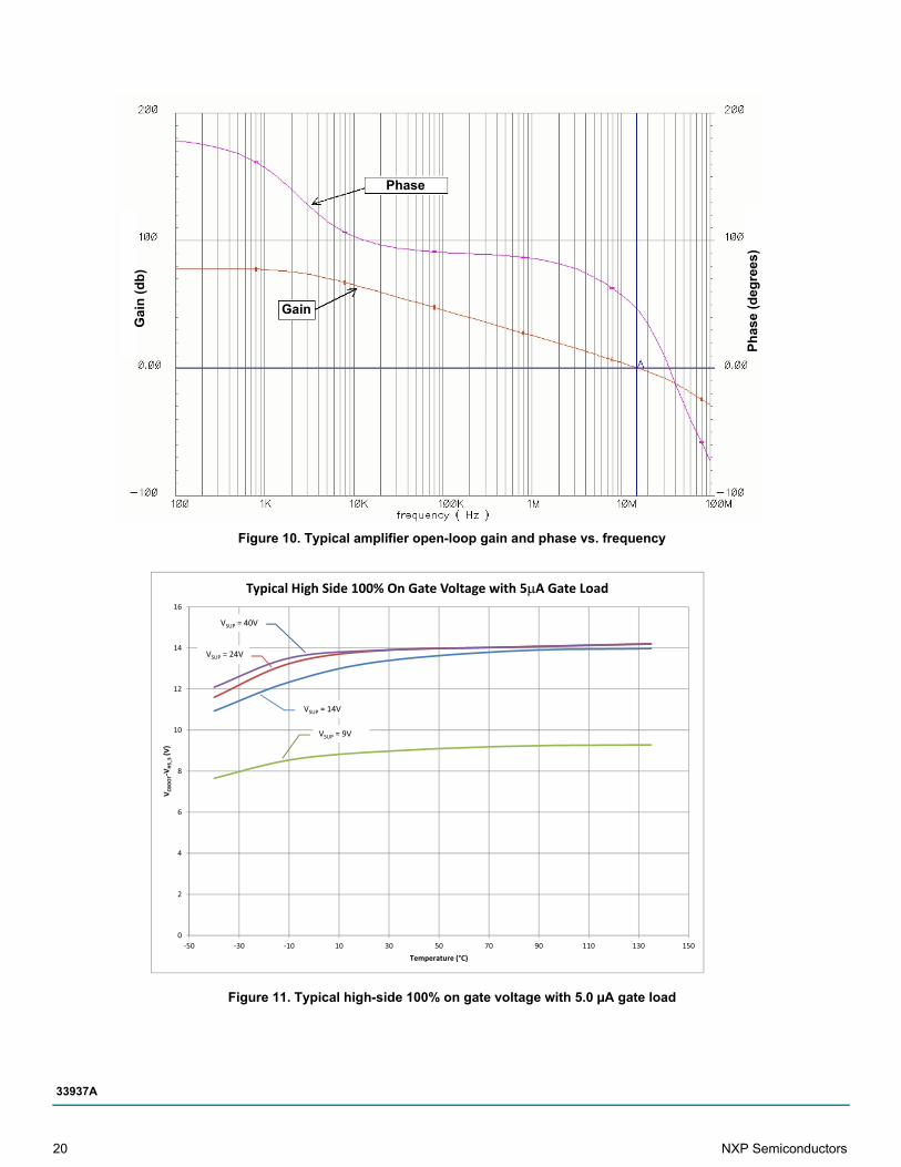
Figure 10. Typical amplifier open-loop gain and phase vs. frequency
Figure 11. Typical high-side 100% on gate voltage with 5.0 µA gate load
Gai
n (
db
)
Ph
ase
(d
egre
es)
Gain
Phase
16
Typical�High�Side�100%�On�Gate�Voltage�with�5�A�Gate�Load
VSUP =�40V
14VSUP =�24V
SUP
10
12
VSUP =�9V
VSUP =�14V
8
VCB
OOT�VHS_S(V)
4
6
2
0�50 �30 �10 10 30 50 70 90 110 130 150
Temperature�(°C)
20 NXP Semiconductors
33937A
5 Functional descriptions
5.1 Introduction
The 33937A provides an interface between an MCU and the large FETs used to drive three phase loads. A typical load FET may have an on resistance of 4.0 mΩ or less and could require a gate charge of over 400 nC to fully turn on. The IC can operate in automotive 12 V to 42 V environments.
Because there are so many methods of controlling three phase systems, the IC enforces few constraints on driving the FETs. It does provide deadtime (cross-over) blanking and logic, both of which can be overridden, ensuring both FETs in a phase are not simultaneously enabled. A SPI port is used to configure the IC modes.
5.2 Functional pin description
5.2.1 Phase A (PHASEA)This pin is the totem pole output of the Phase A comparator. This output is low when the voltage on Phase A high-side source (source of the high-side load FET) is less than 50 percent of VSUP.
5.2.2 Power ground (PGND)This pin is power ground for the charge pump. It should be connected to VSS, however routing to a single point ground on the PCB may help to isolate charge pump noise.
5.2.3 Enable 1 and enable 2 (EN1, EN2)Both of these logic signal inputs must be high to enable any gate drive output. When either or both are low, the internal logic (SPI port, etc.) still functions normally, but all gate drives are forced off (external power FET gates pulled low). The signal is asynchronous.
When EN1 and EN2 return high to enable the outputs, each LS driver must be pulsed ON before the corresponding HS driver can be commanded ON. This ensures that the bootstrap capacitors are charged. See 7.3, Initialization requirements on page 41.
5.2.4 Reset (RST)When the reset pin is low the integrated circuit (IC) is in a low power state. In this mode, all outputs are disabled, internal bias circuits are turned off, and a small pull-down current is applied to the output gate drives. The internal logic will be reset within 77 ns of RESET going low. When RST is low, the IC consumes minimal current.
5.2.5 Charge pump out (PUMP)This pin is the switching node of the charge pump circuit. The output of the internal charge pump support circuit. When the charge pump is used, it is connected to the external pumping capacitor. This pin may be left floating if the charge pump is not required.
5.2.6 Charge pump input (VPUMP)This pin is the input supply for the charge pump circuit. When the charge pump is required, this pin should be connected to a polarity protected supply. This input should never be connected to a supply greater than 40 V. If the charge pump is not required this pin may be left floating.
5.2.7 VSUP input (VSUP)The supply voltage pin should be connected to the common connection of the high-side FETs. It is the reference bias for the Phase Comparators and Desaturation Comparator. It is also used to provide power to the internal steady state trickle charge pump and to energize the hold off circuit.
NXP Semiconductors 21
33937A
5.2.8 Phase B (PHASEB)This pin is the totem pole output of the Phase B comparator. This output is low when the voltage on Phase B high-side source (source of the high-side load FET) is less than 50 percent of VSUP.
5.2.9 Phase C (PHASEC)This pin is the totem pole output of the Phase C comparator. This output is low when the voltage on Phase C high-side source (source of the high-side load FET) is less than 50 percent of VSUP.
5.2.10 Phase A high-side input (PA_HS)This input logic signal pin enables the high-side driver for Phase A. The signal is active low, and is pulled up by an internal current source.
5.2.11 Phase A low-side input (PA_LS)This input logic signal pin enables the low-side driver for Phase A. The signal is active high, and is pulled down by an internal current sink.
5.2.12 VDD Voltage Regulator (VDD)VDD is an internally generated 5.0 V supply. The internal regulator provides continuous power to the IC and is a supply reference for the SPI port. A 0.47 µF (min) decoupling capacitor must be connected to this pin. This regulator is intended for internal IC use and can supply only a small (1.0 mA) external load current. A power-on-reset (POR) circuit monitors this pin and until the voltage rises above the threshold, the internal logic will be reset; driver outputs are tri-stated and SPI communication is disabled. The VDD regulator can be disabled by asserting the RST signal low. The VDD regulator is powered from the VPWR pin.
5.2.13 Phase B high-side control input (PB_HS)This pin is the input logic signal, enabling the high-side driver for Phase B. The signal is active low, and is pulled up by an internal current source.
5.2.14 Phase B low-side input (PB_LS)This pin is the input logic signal, enabling the low-side driver for Phase B. The signal is active high, and is pulled down by an internal current sink.
5.2.15 Interrupt (INT)The Interrupt pin is a totem pole logic output. When a fault is detected, this pin pulls high until it is cleared by executing the Clear Interrupt command via the SPI port. The faults capable of causing an interrupt can be masked via the MASK0 and MASK1 SPI registers to customize the response.
5.2.16 Chip select (CS) Chip select is a logic input that frames the SPI commands and enables the SPI port. This signal is active low, and is pulled up by an internal current source.
5.2.17 Serial in (SI)The Serial In pin is used to input data to the SPI port. Clocked on the falling edge of SCLK, it is the most significant bit (MSB) first. This pin is pulled down by an internal current sink.
22 NXP Semiconductors
33937A
5.2.18 Serial clock (SCLK)This logic input is the clock is used for the SPI port. The SCLK typically runs at 3.0 MHz (up to 5.0 MHz) and is pulled down by an internal current sink.
5.2.19 Serial out (SO)Output data for the SPI port streams from this pin. It is tri-stated until CS is low. New data appears on rising edges of SCLK in preparation for latching by the falling edge of SCLK on the master.
5.2.20 Phase C low-side input (PC_LS)This input logic pin enables the low-side driver for Phase C. This pin is an active high, and is pulled down by an internal current sink.
5.2.21 Phase C high-side input (PC_HS)This input logic pin enables the high-side driver for Phase C. This signal is active low, and is pulled up by an internal current source.
5.2.22 Amplifier output (AMP_OUT)This pin is the output for the current sensing amplifier. It is also the sense input to the overcurrent comparator.
5.2.23 Amplifier inverting input (AMP_N)The inverting input to the current sensing amplifier.
5.2.24 Amplifier non-inverting input (AMP_P)The non-inverting input to the current sensing amplifier.
5.2.25 Overcurrent comparator output (OC_OUT)The overcurrent comparator output is a totem pole logic level output. A logic high indicates an overcurrent condition.
5.2.26 Overcurrent comparator threshold (OC_TH)This input sets the threshold level of the overcurrent comparator.
5.2.27 Voltage source supply (VSS)VSS is the ground reference for the logic interface and power supplies.
5.2.28 Ground (GND0, GND1)These two pins are connected internally to VSS by a 1.0 Ω resistor. They provide device substrate connections and also the primary return path for ESD protection.
5.2.29 VLS regulator capacitor (VLS_CAP)This connection is for a capacitor which provides a low-impedance for switching currents on the gate drive. A low ESR decoupling capacitor, capable of sourcing the pulsed drive currents must be connected between this pin and VSS. This is the same DC node as VLS, but it is physically placed on the opposite end of the IC to minimize the source impedance to the gate drive circuits.
NXP Semiconductors 23
33937A
5.2.30 Phase C low-side source (PC_LS_S)The phase C low-side source is the pin used to return the gate currents from the low-side FET. Best performance is realized by connecting this node directly to the source of the low-side FET for phase C.
5.2.31 Phase C low-side gate (PC_LS_G)This is the gate drive for the Phase C low-side output FET. It provides high-current through a low-impedance to turn on and off the low-side FET. A low-impedance drive ensures transient currents do not overcome an off-state driver and allow pulses of current to flow in the external FET. This output has also been designed to resist the influence of negative currents.
5.2.32 Phase C high-side source (PC_HS_S)The source connection for the Phase C high-side output FET is the reference voltage for the gate drive on the high-side FET and also the low-voltage end of the bootstrap capacitor.
5.2.33 Phase C high-side gate (PC_HS_G)This is the gate drive for the Phase C high-side output FET. This pin provides the gate bias to turn the external FET on or off. The gate voltage is limited to about 15 V above the FET source voltage. A low-impedance drive is used, ensuring transient currents do not overcome an off-state driver and allow pulses of current to flow in the external FETs. This output has also been designed to resist the influence of negative currents.
5.2.34 Phase C bootstrap (PC_BOOT)This is the bootstrap capacitor connection for Phase C. A capacitor connected between PC_HS_S and this pin provides the gate voltage and current to drive the external FET gate. Typically, the bootstrap capacitor selection is 10 to 20 times the gate capacitance. The voltage across this capacitor is limited to about 15 V.
5.2.35 Phase B low-side source (PB_LS_S)The Phase B low-side source is the pin used to return the gate currents from the Low-side FET. Best performance is realized by connecting this node directly to the source of the low-side FET for Phase B.
5.2.36 Phase B low-side gate (PC_LS_G)This is the gate drive for the Phase B low-side output FET. It provides high-current through a low-impedance to turn on and off the low-side FET. A low-impedance drive ensures transient currents do not overcome an off-state driver and allow pulses of current to flow in the external FET. This output has also been designed to resist the influence of negative currents.
5.2.37 Phase B high-side source (PB_HS_S)The source connection for the Phase B high-side output FET is the reference voltage for the gate drive on the high-side FET and also the low-voltage end of the bootstrap capacitor.
5.2.38 Phase B high-side gate (PB_HS_G)This is the gate drive for the Phase B high-side output FET. This pin provides the gate bias to turn the external FET on or off. The gate voltage is limited to about 15 V above the FET source voltage. A low-impedance drive is used, ensuring transient currents do not overcome an off-state driver and allow pulses of current to flow in the external FETs. This output has also been designed to resist the influence of negative currents.
24 NXP Semiconductors
33937A

5.2.39 Phase B bootstrap (PB_BOOT)This is the bootstrap capacitor connection for phase B. A capacitor connected between PC_HS_S and this pin provides the gate voltage and current to drive the external FET gate. Typically, the bootstrap capacitor selection is 10 to 20 times the gate capacitance. The voltage across this capacitor is limited to about 15 V.
5.2.40 PHASE A low-side source (PA_LS_S)The Phase A low-side source is the pin used to return the gate currents from the low-side FET. Best performance is realized by connecting this node directly to the source of the low-side FET for phase A.
5.2.41 Phase A low-side gate (PA_LS_G)This is the gate drive for the Phase A low-side output FET. It provides high-current through a low-impedance to turn on and off the low-side FET. A low-impedance drive ensures transient currents do not overcome an off-state driver and allow pulses of current to flow in the external FET. This output has also been designed to resist the influence of negative currents.
5.2.42 Phase A high-side source (PA_HS_S)The source connection for the Phase A high-side output FET is the reference voltage for the gate drive on the high-side FET and also the low-voltage end of the bootstrap capacitor.
5.2.43 Phase A high-side gate (PA_HS_G)This is the gate drive for the Phase A high-side output FET. This pin provides the gate bias to turn the external FET on or off. The gate voltage is limited to about 15 V above the FET source voltage. A low-impedance drive is used, ensuring transient currents do not overcome an off-state driver and allow pulses of current to flow in the external FETs. This output has also been designed to resist the influence of negative currents.
5.2.44 Phase A bootstrap (PA_BOOT)This is the bootstrap capacitor connection for phase A. A capacitor connected between PC_HS_S and this pin provides the gate voltage and current to drive the external FET gate. Typically, the bootstrap capacitor selection is 10 to 20 times the gate capacitance. The voltage across this capacitor is limited to about 15 V.
5.2.45 VLS regulator (VLS)VLS is the gate drive power supply regulated at approximately 15 V. This is an internally generated supply from VPWR. It is the source for the low-side gate drive voltage, and also the high-side bootstrap source. A low ESR decoupling capacitor, capable of sourcing the pulsed drive currents, must be connected between this pin and VSS.
5.2.46 VPWR input (VPWR)VPWR is the power supply input for VLS and VDD. Current flowing into this input recharges the bootstrap capacitors as well as supplying power to the low-side gate drivers and the VDD regulator. An internal regulator regulates the actual gate voltages. This pin can be connected to system battery voltage if power dissipation is not a concern.
5.2.47 Exposed pad (EP)The primary function of the exposed pad is to conduct heat out of the device. This pad may be connected electrically to the substrate of the device.The device performs as specified with the exposed pad un-terminated (floating). However, it is recommended the exposed pad be terminated to pin 29 (VSS) and the system ground.
NXP Semiconductors 25
33937A
6 Functional internal block description
Figure 12. Functional internal block description
All functions of the IC can be described as the following five major functional blocks:
• Logic Inputs and Interface• Bootstrap Supply• Low-side Drivers• High-side Drivers• Charge Pump
6.1 Logic inputs and interface
This section contains the SPI port, control logic, and shoot-through timers.
The IC logic inputs have Schmitt trigger inputs with hysteresis. Logic inputs are 3.0 V compatible. The logic outputs are driven from the internal supply of approximately 5.0 V. The SPI registers and functionality is described completely in 7.2, Logic commands and registers on page 35. SPI functionality includes the following:
• Programming of deadtime delay—This delay is adjustable in approximately 50 ns steps from 0 ns to 12 µs. Calibration of the delay, because of internal IC variations, is performed via the SPI.
• Enabling of simultaneous operation of high-side and low-side FETs—Normally, both FETs would not be enabled simultaneously. However, for certain applications where the load is connected between the high-side and low-side FETs, this could be advantageous. If this mode is enabled, the blanking time delay will be disabled. A sequence of commands may be required to enable this function to prevent inadvertent enabling. In addition, this command can only be executed once after reset to enable or disable simultaneous turn-on.
• Setting of various operating modes of the IC and enabling of interrupt sources. The 33937A allows different operating modes to be set and locked by an SPI command (FULLON, Desaturation Fault, Zero Deadtime). SPI commands can also determine how the various faults are (or are not) reported.
MC33937 - Functional Block Diagram
Integrated Supply Sensing & Protection Drivers
High Side and Low Side OutputPre-drivers
Logic & Control
Integrated SupplyTrickle Charge Pump
5V Regulator VLS RegulatorMain Charge Pump
Sensing & ProtectionHold-off
TemperatureCurrent Sense
Over-current
De-satPhase
Under-voltage
Logic & ControlDead TimeFault Register
Mode ControlPhase ControlSPI Communication
26 NXP Semiconductors
33937A
• Read back of internal registers. The status of the 33937A status registers can be read back by the Master (DSP or MCU).
The Px_HS and Px_LS logic inputs are edge sensitive. This means the leading edge on an input causes the complementary output to immediately turn off and the selected one to turn on after the deadtime delay as illustrated in Figure 13. The deadtime delay timer always starts at the time a FET is commanded off and prevents the complementary FET from being commanded on until after the deadtime has elapsed. Commands to turn on the complementary FET after the deadtime has elapsed are executed immediately without any further delay (see Figure 6 and Figure 13).
Figure 13. Edge sensitive logic inputs (phase A)
6.1.1 Low-side and bootstrap supply (VLS)This is the portion of the IC providing current to recharge the bootstrap capacitors. It also supplies the peak currents required for the low-side gate drivers. The power for the gate drive circuits is provided by VLS which is supplied from the VPWR pin. This pin can be connected to system battery voltage and is capable of withstanding up to the full load dump voltage of the system. However, the IC only requires a low-voltage supply on this pin, typically 13 V to 16 V. Higher voltages on this pin increases the IC power dissipation.
In 12 V systems, the supply voltage can fall as low as 6.0 V. This limits the gate voltage capable of being applied to the FETs and reduces system performance due to the higher FET on-resistance. To allow a higher gate voltage to be supplied, the IC also incorporates a charge pump. The switches and control circuitry are internal; the capacitors and diodes are external (see Figure 22).
6.1.2 Low-side driversThese three drivers turn on and off the external Low-side FETs. The circuits provide a low-impedance drive to the gate, ensuring the FETs remain off in the presence of high dV/dt transients on their drains. Additionally, these output drivers isolate the other portions of the IC from currents capable of being injected into the substrate due to rapid dV/dt transients on the FET drains.
Low-side drivers switch power from VLS to the gates of the Low-side FETs. The Low-side drivers are capable of providing a typical peak current of 2.0 A. This gate drive current may be limited by external resistors in order to achieve a good trade-off between the efficiency and EMC (Electro-Magnetic Compatibility) compliance of the application. the low-side driver uses high-side PMOS for turn on and low-side isolated LDMOS for turn off. The circuit ensures the impedance of the driver remains low, even during periods of reduced current. Current limit is blanked immediately after subsequent input state change to ensure device stays off during dV/dt transients.
6.1.3 High-side driversThese three drivers switch the voltage across the bootstrap capacitor to the external high-side FETs. The circuits provide a low-impedance drive to the gate, ensuring the FETs remain off in the presence of high dV/dt transients on their sources. Further, these output drivers isolate the other portions of the IC from currents capable of being injected into the substrate due to rapid dV/dt transients on the FETs.
The high-side drivers deliver power from their bootstrap capacitor to the gate of the external high-side FET, thus turning the high-side FET on. The high-side driver uses a level shifter, allowing the gate of the external high-side FET to be turned off by switching to the high-side FET source.
PA_HS
PA_LS
PA_HS_G
PA_LS_G
De adt imeDe lay
NXP Semiconductors 27
33937A
The gate supply voltage for the high-side drivers is obtained from the bootstrap supply, so, a short time is required after the application of power to the IC to charge the bootstrap capacitors. To ensure this occurrence, the internal control logic does not allow a high-side switch to be turned on after entering the ENABLE state until the corresponding low-side switch is enabled at least once. Caution must be exercised after a long period of inactivity of the low-side switches to verify the bootstrap capacitor is not discharged. It is charged by activating the low-side switches for a brief period, or by attaching external bleed resistors from the HS_S pins to GND. See 7.3, Initialization requirements on page 41.
In order to achieve a 100% duty cycle operation of the high-side external FETs, a fully integrated trickle charge pump provides the charge necessary to maintain the external FET gates at fully enhanced levels. The trickle charge pump has limited ability to supply external leakage paths while performing it’s primary function. The graph in Figure 11 shows the typical margin for supplying external current loads. These limits are based on maintaining the voltage at CBOOT at least 3.0 V greater than the voltage on the HS_S for that phase. If this voltage differential becomes less than 3.0 V, the corresponding high-side FET most likely does not remain fully enhanced and the high-side driver may malfunction due to insufficient bias voltage between CBOOT and HS_S.
The slew rate of the external output FET is limited by the driver output impedance, overall (external and internal) gate resistance and the load capacitance. To ensure the low-side FET is not turned on by a large positive dV/dt on the drain of the low-side FET, the turn-on slew rate of the high-side should be limited. If the slew rate of the high-side is limited by the gate-drain capacitance of the high-side FET, then the displacement current injected into the low-side gate drive output is approximately the same value. Therefore, to ensure the low-side drivers can be held off, the voltage drop across the low-side gate driver must be lower than the threshold voltage of the low-side FET (see Figure 14).
Similarly, during large negative dV/dt, the high-side FET is able to remain off if its gate drive low-side switch, develops a voltage drop less than the threshold voltage of the high-side FET. The gate drive low-side switch discharges the gate to the source. Additionally, during negative dV/dt the low-side gate drive could be forced below ground. The low-side FETs must not inject detrimental substrate currents in this condition. The occurrence of these cases depends on the polarity of the load current during switching.
Figure 14. Positive DV/dt transient
Phase xOutput
PhaseReturn
Px_LS_S
Px_LS_G
Px_HS_S
Low-SideDriverLS
Control
Px_LS_G
Px_HS_G
Deadtime
-VD
VSUP Phase x Output Voltage
dV/dt
CGS
CDG
CDSRg
iCDG
VLS
33927
+-G
S
D
DiscreteFETPackage
Zo
33937A
28 NXP Semiconductors
33937A
6.1.4 Driver fault protectionThe 33937A IC integrates several protection mechanisms against various faults. The first of them is the current sense amplifier with the overcurrent comparator. These two blocks are common for all three driver phases.
6.1.4.1 Current sense amplifier
This amplifier is usually connected as a differential amplifier (see Figure 9). It senses a current flowing through the external FETs as a voltage across the current sense resistor RSENSE. Since the amplifier common mode range does not extend below ground, it is necessary to use an external reference to permit measuring both positive and negative currents. The amplifier output can be monitored directly (e.g. by the microcontroller’s ADC) at the AMP_OUT pin, providing the means for closed loop control with the 33937A. The output voltage is internally compared with the overcurrent comparator threshold voltage (see Figure 22).
6.1.4.2 Overcurrent comparator
The amplified voltage across RSENSE is compared with the pre-set threshold value by the overcurrent comparator input. If the current sense amplifier output voltage exceeds the threshold of the overcurrent comparator, it would change the status of its output (OC_OUT pin) and the fault condition would be latched (see 7.2.3.2Figure 18).
The occurrence of this fault would be signalled by the return value of the Status Register 0. If the proper interrupt mask has been set, this fault condition generates an interrupt - the INT pin asserts High. The INT is held in the High state until the fault is removed, and the appropriate bit in the Status Register 0 is cleared by the CLINT0 command. This fault reporting technique is described in detail in 7.2, Logic commands and registers on page 35.
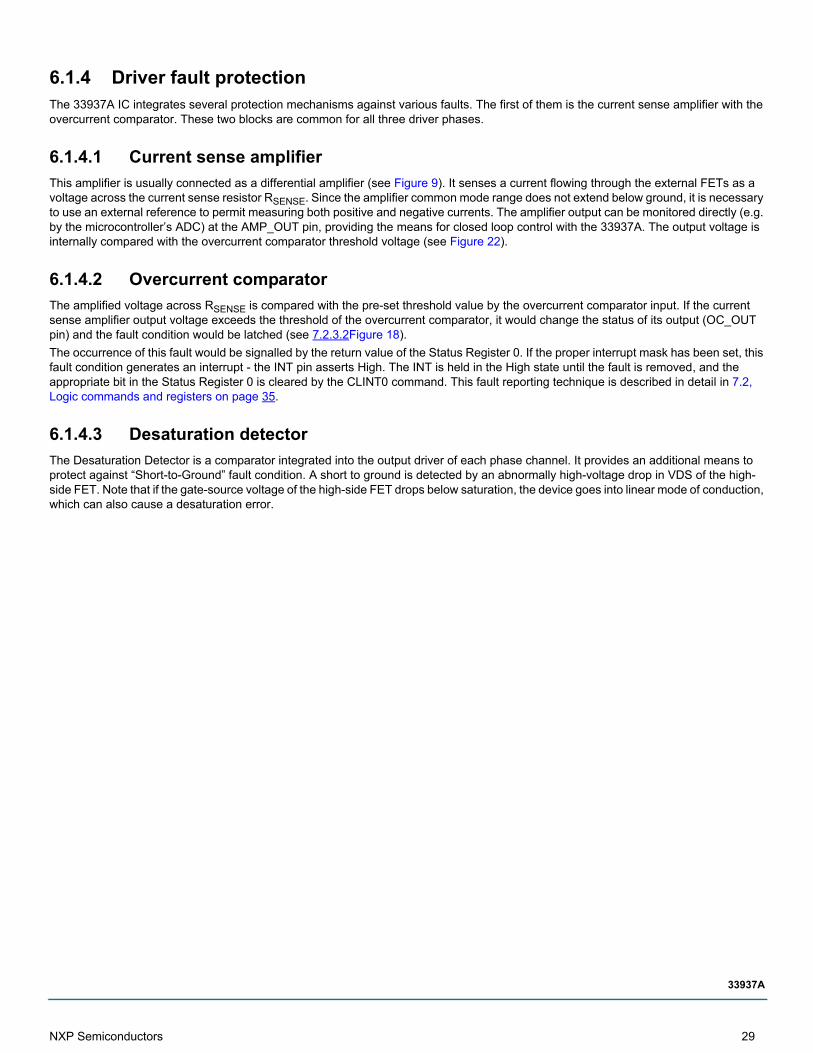
6.1.4.3 Desaturation detector
The Desaturation Detector is a comparator integrated into the output driver of each phase channel. It provides an additional means to protect against “Short-to-Ground” fault condition. A short to ground is detected by an abnormally high-voltage drop in VDS of the high-side FET. Note that if the gate-source voltage of the high-side FET drops below saturation, the device goes into linear mode of conduction, which can also cause a desaturation error.
NXP Semiconductors 29
33937A
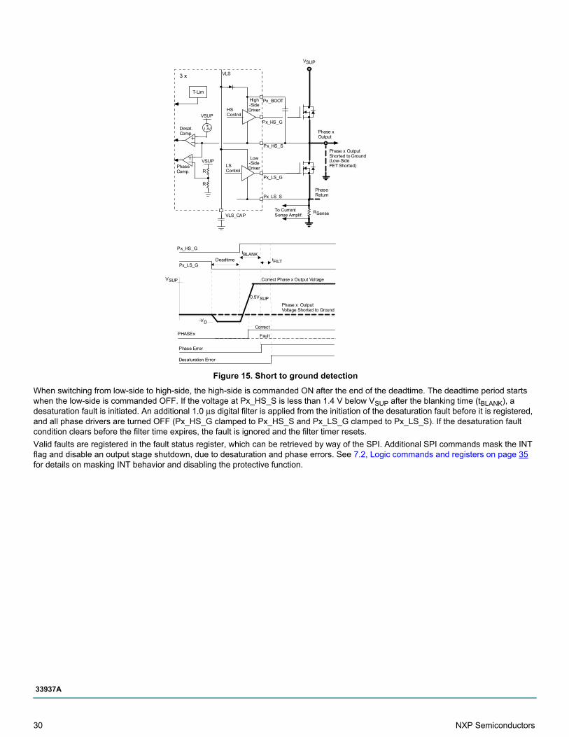
Figure 15. Short to ground detection
When switching from low-side to high-side, the high-side is commanded ON after the end of the deadtime. The deadtime period starts when the low-side is commanded OFF. If the voltage at Px_HS_S is less than 1.4 V below VSUP after the blanking time (tBLANK), a desaturation fault is initiated. An additional 1.0 μs digital filter is applied from the initiation of the desaturation fault before it is registered, and all phase drivers are turned OFF (Px_HS_G clamped to Px_HS_S and Px_LS_G clamped to Px_LS_S). If the desaturation fault condition clears before the filter time expires, the fault is ignored and the filter timer resets.
Valid faults are registered in the fault status register, which can be retrieved by way of the SPI. Additional SPI commands mask the INT flag and disable an output stage shutdown, due to desaturation and phase errors. See 7.2, Logic commands and registers on page 35 for details on masking INT behavior and disabling the protective function.
VSUP
Phase xOutput
RSense
PhaseReturn
T-Lim
VLS_CAP
Px_LS_S
Px_LS_G
Px_HS_G
Px_HS_S
Px_BOOT
PhaseComp.
Desat.Comp.
3 x
+-
VSUP
VSUP
1.4V
Low-SideDriver
High-SideDriverHS
Control
R
R
VLS
To CurrentSense Amplif.
Phase x OutputShorted to Ground(Low-SideFET Shorted)LS
Control
Px_LS_G
Px_HS_G
Deadtime
-VD
VSUP
Phase x OutputVoltage Shorted to Ground
Correct Phase x Output Voltage
0.5VSUP
PHASEx
Correct
Fault
Phase Error
tBLANKtFILT
Desaturation Error
30 NXP Semiconductors
33937A
Figure 16. Short to supply detection
6.1.4.4 Phase comparator
Faults could also be detected as phase errors. A phase error is generated if the output signal (at Px_HS_S) does not properly reflect the drive conditions.
A phase error is detected by a Phase comparator. The Phase comparator compares the voltage at the Px_HS_S node with a reference of one half the voltage at the VSUP pin. A high-side phase error (which also triggers the Desaturation Detector) occurs when the high-side FET is commanded on, and Px_HS_S is still low at the end of the deadtime and blanking time duration. Similarly, a LS phase error occurs when the low-side FET is commanded on, and the Px_HS_S is still high at the end of the deadtime and blanking time duration.
The Phase Error flag is the triple OR of phase errors from each phase. Each phase error is the OR of the high-side and low-side phase errors. This flag can generate an interrupt if the appropriate mask bit is set. The INT is held in the high state until the fault is removed, and the appropriate bit in the Status Register 0 is cleared by the CLINT1 command. This fault reporting mechanism is described in detail in 7.2, Logic commands and registers on page 35.
6.1.5 VLS undervoltageSince VLS supplies both the gate driver circuits and the gate voltage, it is critical it maintains sufficient potential to place the power stage FETs in saturation. Since proper operation cannot continue with insufficient levels, a low VLS condition shuts down driver operation. The VLS undervoltage threshold is between 7.5 V and 8.5 V. When a decreasing level reaches the threshold, both the HS and the LS output gate circuit drive the gates OFF for about 8.0 μs before reducing the drive to hold off levels. Since low VLS is a condition for turning on the Hold Off circuit, Hold Off then provides a weak pull-down on all gates. A filter timeout of about 700 ns insures noise on VLS does not cause premature protective action.
VSUP
Phase xOutput
RSense
PhaseReturn
T-Lim
VLS_CAP
Px_LS_S
Px_LS_G
Px_HS_G
Px_HS_S
Px_BOOT
PhaseComp.
Desat.Comp.
3 x
+-
VSUP
VSUP
1.4V
Low-SideDriver
High-SideDriverHS
Control
R
R
VLS
To CurrentSense Amplif.
Phase x OutputShorted to VSUP(High-SideFET Shorted)
LSControl
Px_LS_G
Px_HS_G
Deadtime
-VD
VSUP Phase x Output Voltage Shorted to VSUP
Correct Phase x Output Voltage
0.5VSUP
PHASEx Correct
Fault
Phase Error
tBLANK
NXP Semiconductors 31
33937A
When VLS rises above this threshold again, the LS Gate immediately follows the level of the input. However, a short initialization sequence must be executed to restore operation of the HS Gate. (See 7.3, Initialization requirements on page 41) Since VLS is no longer undervoltage, the Hold Off circuit is turned off and the HS Gate is in a high-impedance state until the LS Gate responds to an input command to turn off.
6.1.6 Hold off circuitThe IC guarantees the output FETs are turned off in the absence of VDD or VPWR by means of the Hold off circuit. A small current source, generated from VSUP, typically 100 µA, is mirrored and pulls all the output gate drive pins low when VDD is less than about 3.0 V, RST is active (low), or when VLS is lower than the VLS_Disable threshold. A minimum of 3.0 V is required on VSUP to energize the Hold off circuit.
6.1.7 Charge pumpThe charge pump circuit provides the basic switching elements required to implement a charge pump, when combined with external capacitors and diodes for enhanced low-voltage operation. When the 33937A is connected per the typical application using the charge pump (see Figure 22), the regulation path for VLS includes the charge pump and a linear regulator. The regulation set point for the linear regulator is nominally at 15.34 V. As long as VLS output voltage (VLSOUT) is greater than the VLS analog regulator threshold (VLSATH) minus VTHREG, the charge pump is not active.
If VLSOUT < VLSATH – VTHREG the charge pump turns ON until VLSOUT > VLSATH – VTHREG + VHYST
VHYST is approximately 200 mV. VLSATH does not interfere with this cycle even when there is overlap in the thresholds, due to the design of the regulator system. The maximum current the charge pump can supply is dependent on the pump capacitor value and quality, the pump frequency (nominally 130 kHz), and the RDS(on) of the pump FETs. The effective charge voltage for the pump capacitor would be VSYS – 2 * VDIODE. The total charge transfer would then be CPUMP * (VSYS – 2*VDIODE). Multiplying by the switch frequency gives the theoretical current the pump can transfer: FPUMP * CPUMP * (VSYS – 2*VDIODE).
NOTE: There is also another smaller, fully integrated charge pump (Trickle Charge Pump - see Figure 2), which is used to maintain the high-side drivers’ gate VGS in 100 percent duty cycle modes.
32 NXP Semiconductors
33937A
7 Functional device operation
7.1 Operational modes
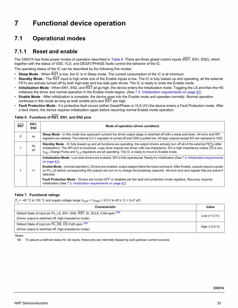
7.1.1 Reset and enableThe 33937A has three power modes of operation described in Table 6. There are three global control inputs (RST, EN1, EN2), which together with the status of VDD, VLS, and DESAT/PHASE faults control the behavior of the IC.
The operating status of the IC can be described by the following five modes:
• Sleep Mode - When RST is low, the IC is in Sleep mode. The current consumption of the IC is at minimum.• Standby Mode - The RST input is high while one of the Enable inputs is low. The IC is fully biased up and operating, all the external
FETs are actively turned off by both high-side and low-side gate drives. The IC is ready to enter the Enable mode.• Initialization Mode - When EN1, EN2, and RST all go high, the device enters the Initialization mode. Toggling the LS and then the HS
initializes the driver and normal operation in the Enable mode begins. (See 7.3, Initialization requirements on page 41) • Enable Mode - After initialization is complete, the device goes into the Enable mode and operates normally. Normal operation
continues in this mode as long as both enable pins and RST are high.• Fault Protection Mode - If a protective fault occurs (either Desat/Phase or VLS UV) the device enters a Fault Protection mode. After
a fault clears, the device requires initialization again before resuming normal Enable mode operation.
Table 6. Functions of RST, EN1, and EN2 pins
RST EN1, EN2
Mode of operation (driver condition)
0 xxSleep Mode - in this mode (low quiescent current) the driver output stage is switched-off with a weak pull-down. All error and SPI registers are cleared. The internal 5.0 V regulator is turned off and VDD is pulled low. All logic outputs except SO are clamped to VSS.
10xx0
Standby Mode - IC fully biased up and all functions are operating, the output drivers actively turn off all of the external FETs (after initialization). The SPI port is functional. Logic level outputs are driven with low-impedance. SO is high-impedance unless CS is low. VDD, Charge Pump and VLS regulators are all operating. The IC is ready to move to Enable mode.
1 11
Initialization Mode - Low-side drivers are enabled, SPI is fully operational. Ready for initialization (See 7.3, Initialization requirements on page 41).
Enable Mode - (normal operation). Drivers are enabled; output stages follow the input command. After Enable, outputs require a pulse on Px_LS before corresponding HS outputs are turn on to charge the bootstrap capacitor. All error pins and register bits are active if detected.
Fault Protection Mode - Drivers are turned OFF or disabled per the fault and protection mode registers. Recovery requires initialization (See 7.3, Initialization requirements on page 41).
Table 7. Functional ratings
(TJ = -40 °C to 150 °C and supply voltage range VSUP = VPWR = 5.0 V to 45 V, C = 0.47 µF)
Characteristic Value
Default State of input pin Px_LS, EN1, EN2, RST, SI, SCLK, if left open (58)
(Driver output is switched off, high-impedance mode)Low (<1.0 V)
Default State of input pin Px_HS, CS if left open (58)
(Driver output is switched off, high-impedance mode)High (>2.0 V)
Notes58. To assure a defined status for all inputs, these pins are internally biased by pull-up/down current sources.
NXP Semiconductors 33
33937A
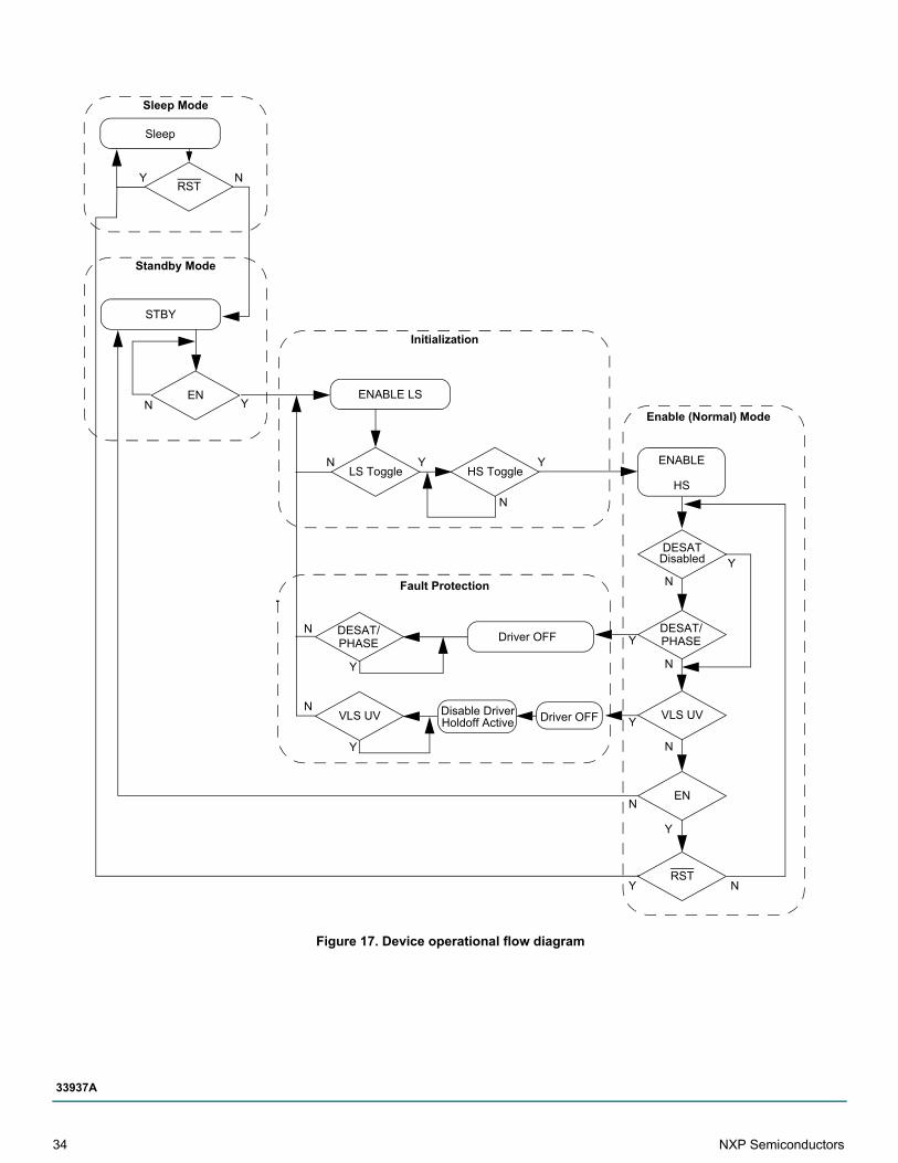
Figure 17. Device operational flow diagram
Sleep Mode
Initialization
Standby Mode
Fault Protection
Enable (Normal) Mode
Sleep
RSTNY
STBY
ENYN
ENABLE LS
LS Toggle HS ToggleYN Y
N
Driver OFF
Disable Driver
DESAT/
VLS UV
Y
Y
N
N
ENABLE
HS
DESAT
VLS UV
EN
RST
Disabled
N
N
N
Y
Y
Y
Y
N
Y
N
Holdoff Active
PHASEDESAT/PHASE
Driver OFF
34 NXP Semiconductors
33937A
7.2 Logic commands and registers
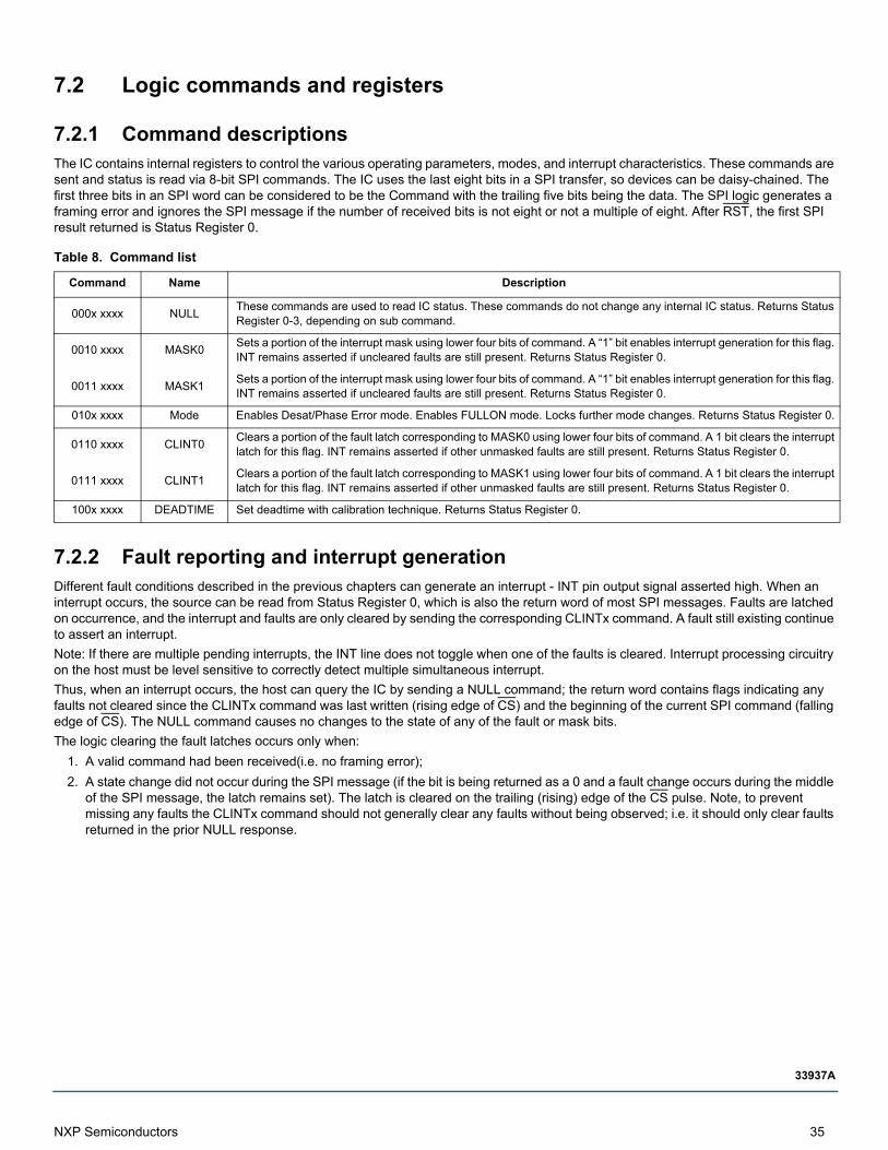
7.2.1 Command descriptionsThe IC contains internal registers to control the various operating parameters, modes, and interrupt characteristics. These commands are sent and status is read via 8-bit SPI commands. The IC uses the last eight bits in a SPI transfer, so devices can be daisy-chained. The first three bits in an SPI word can be considered to be the Command with the trailing five bits being the data. The SPI logic generates a framing error and ignores the SPI message if the number of received bits is not eight or not a multiple of eight. After RST, the first SPI result returned is Status Register 0.
7.2.2 Fault reporting and interrupt generationDifferent fault conditions described in the previous chapters can generate an interrupt - INT pin output signal asserted high. When an interrupt occurs, the source can be read from Status Register 0, which is also the return word of most SPI messages. Faults are latched on occurrence, and the interrupt and faults are only cleared by sending the corresponding CLINTx command. A fault still existing continue to assert an interrupt.
Note: If there are multiple pending interrupts, the INT line does not toggle when one of the faults is cleared. Interrupt processing circuitry on the host must be level sensitive to correctly detect multiple simultaneous interrupt.
Thus, when an interrupt occurs, the host can query the IC by sending a NULL command; the return word contains flags indicating any faults not cleared since the CLINTx command was last written (rising edge of CS) and the beginning of the current SPI command (falling edge of CS). The NULL command causes no changes to the state of any of the fault or mask bits.
The logic clearing the fault latches occurs only when:
1. A valid command had been received(i.e. no framing error);
2. A state change did not occur during the SPI message (if the bit is being returned as a 0 and a fault change occurs during the middle of the SPI message, the latch remains set). The latch is cleared on the trailing (rising) edge of the CS pulse. Note, to prevent missing any faults the CLINTx command should not generally clear any faults without being observed; i.e. it should only clear faults returned in the prior NULL response.
Table 8. Command list
Command Name Description
000x xxxx NULLThese commands are used to read IC status. These commands do not change any internal IC status. Returns Status Register 0-3, depending on sub command.
0010 xxxx MASK0Sets a portion of the interrupt mask using lower four bits of command. A “1” bit enables interrupt generation for this flag. INT remains asserted if uncleared faults are still present. Returns Status Register 0.
0011 xxxx MASK1Sets a portion of the interrupt mask using lower four bits of command. A “1” bit enables interrupt generation for this flag. INT remains asserted if uncleared faults are still present. Returns Status Register 0.
010x xxxx Mode Enables Desat/Phase Error mode. Enables FULLON mode. Locks further mode changes. Returns Status Register 0.
0110 xxxx CLINT0Clears a portion of the fault latch corresponding to MASK0 using lower four bits of command. A 1 bit clears the interrupt latch for this flag. INT remains asserted if other unmasked faults are still present. Returns Status Register 0.
0111 xxxx CLINT1Clears a portion of the fault latch corresponding to MASK1 using lower four bits of command. A 1 bit clears the interrupt latch for this flag. INT remains asserted if other unmasked faults are still present. Returns Status Register 0.
100x xxxx DEADTIME Set deadtime with calibration technique. Returns Status Register 0.
NXP Semiconductors 35
33937A
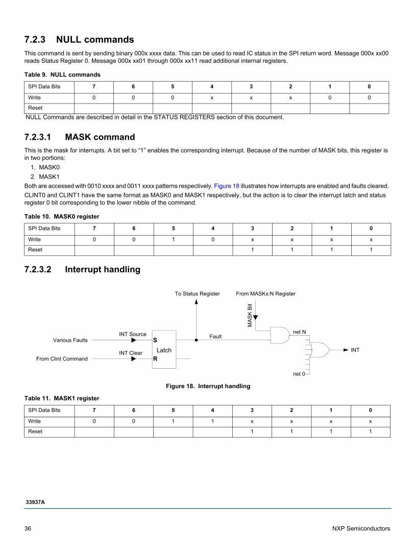
7.2.3 NULL commandsThis command is sent by sending binary 000x xxxx data. This can be used to read IC status in the SPI return word. Message 000x xx00 reads Status Register 0. Message 000x xx01 through 000x xx11 read additional internal registers.
7.2.3.1 MASK command
This is the mask for interrupts. A bit set to “1” enables the corresponding interrupt. Because of the number of MASK bits, this register is in two portions:
1. MASK0
2. MASK1
Both are accessed with 0010 xxxx and 0011 xxxx patterns respectively. Figure 18 illustrates how interrupts are enabled and faults cleared.
CLINT0 and CLINT1 have the same format as MASK0 and MASK1 respectively, but the action is to clear the interrupt latch and status register 0 bit corresponding to the lower nibble of the command.
7.2.3.2 Interrupt handling
Figure 18. Interrupt handling
Table 9. NULL commands
SPI Data Bits 7 6 5 4 3 2 1 0
Write 0 0 0 x x x 0 0
Reset
NULL Commands are described in detail in the STATUS REGISTERS section of this document.
Table 10. MASK0 register
SPI Data Bits 7 6 5 4 3 2 1 0
Write 0 0 1 0 x x x x
Reset 1 1 1 1
Table 11. MASK1 register
SPI Data Bits 7 6 5 4 3 2 1 0
Write 0 0 1 1 x x x x
Reset 1 1 1 1
To Status Register
Various Faults
From Clint Command
From MASKx:N Register
Fault
net 0
net N
INT
MA
SK
Bit
INT Clear
INT SourceS
R
Latch
36 NXP Semiconductors
33937A
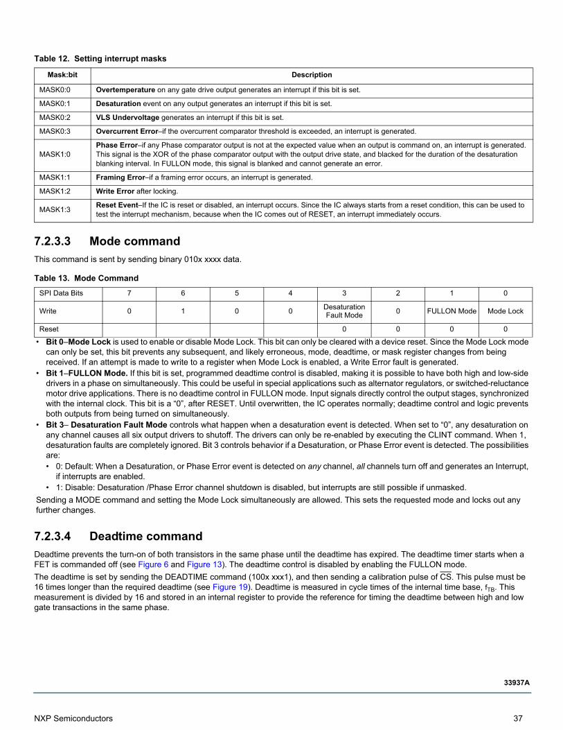
7.2.3.3 Mode command
This command is sent by sending binary 010x xxxx data.
7.2.3.4 Deadtime command
Deadtime prevents the turn-on of both transistors in the same phase until the deadtime has expired. The deadtime timer starts when a FET is commanded off (see Figure 6 and Figure 13). The deadtime control is disabled by enabling the FULLON mode.
The deadtime is set by sending the DEADTIME command (100x xxx1), and then sending a calibration pulse of CS. This pulse must be 16 times longer than the required deadtime (see Figure 19). Deadtime is measured in cycle times of the internal time base, fTB. This measurement is divided by 16 and stored in an internal register to provide the reference for timing the deadtime between high and low gate transactions in the same phase.
Table 12. Setting interrupt masks
Mask:bit Description
MASK0:0 Overtemperature on any gate drive output generates an interrupt if this bit is set.
MASK0:1 Desaturation event on any output generates an interrupt if this bit is set.
MASK0:2 VLS Undervoltage generates an interrupt if this bit is set.
MASK0:3 Overcurrent Error–if the overcurrent comparator threshold is exceeded, an interrupt is generated.
MASK1:0Phase Error–if any Phase comparator output is not at the expected value when an output is command on, an interrupt is generated. This signal is the XOR of the phase comparator output with the output drive state, and blacked for the duration of the desaturation blanking interval. In FULLON mode, this signal is blanked and cannot generate an error.
MASK1:1 Framing Error–if a framing error occurs, an interrupt is generated.
MASK1:2 Write Error after locking.
MASK1:3Reset Event–If the IC is reset or disabled, an interrupt occurs. Since the IC always starts from a reset condition, this can be used to test the interrupt mechanism, because when the IC comes out of RESET, an interrupt immediately occurs.
Table 13. Mode Command
SPI Data Bits 7 6 5 4 3 2 1 0
Write 0 1 0 0Desaturation Fault Mode
0 FULLON Mode Mode Lock
Reset 0 0 0 0
• Bit 0–Mode Lock is used to enable or disable Mode Lock. This bit can only be cleared with a device reset. Since the Mode Lock mode can only be set, this bit prevents any subsequent, and likely erroneous, mode, deadtime, or mask register changes from being received. If an attempt is made to write to a register when Mode Lock is enabled, a Write Error fault is generated.
• Bit 1–FULLON Mode. If this bit is set, programmed deadtime control is disabled, making it is possible to have both high and low-side drivers in a phase on simultaneously. This could be useful in special applications such as alternator regulators, or switched-reluctance motor drive applications. There is no deadtime control in FULLON mode. Input signals directly control the output stages, synchronized with the internal clock. This bit is a “0”, after RESET. Until overwritten, the IC operates normally; deadtime control and logic prevents both outputs from being turned on simultaneously.
• Bit 3– Desaturation Fault Mode controls what happen when a desaturation event is detected. When set to “0”, any desaturation on any channel causes all six output drivers to shutoff. The drivers can only be re-enabled by executing the CLINT command. When 1, desaturation faults are completely ignored. Bit 3 controls behavior if a Desaturation, or Phase Error event is detected. The possibilities are: • 0: Default: When a Desaturation, or Phase Error event is detected on any channel, all channels turn off and generates an Interrupt,
if interrupts are enabled.• 1: Disable: Desaturation /Phase Error channel shutdown is disabled, but interrupts are still possible if unmasked.
Sending a MODE command and setting the Mode Lock simultaneously are allowed. This sets the requested mode and locks out any further changes.
NXP Semiconductors 37
33937A
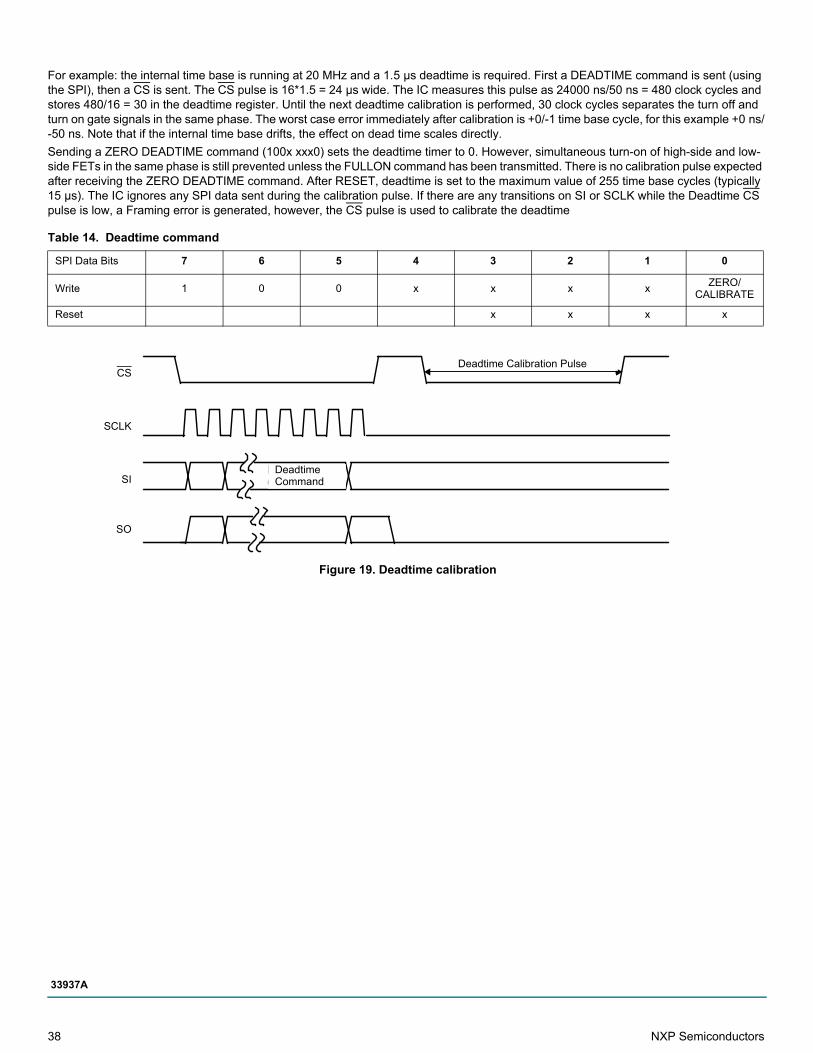
For example: the internal time base is running at 20 MHz and a 1.5 µs deadtime is required. First a DEADTIME command is sent (using the SPI), then a CS is sent. The CS pulse is 16*1.5 = 24 µs wide. The IC measures this pulse as 24000 ns/50 ns = 480 clock cycles and stores 480/16 = 30 in the deadtime register. Until the next deadtime calibration is performed, 30 clock cycles separates the turn off and turn on gate signals in the same phase. The worst case error immediately after calibration is +0/-1 time base cycle, for this example +0 ns/-50 ns. Note that if the internal time base drifts, the effect on dead time scales directly.
Sending a ZERO DEADTIME command (100x xxx0) sets the deadtime timer to 0. However, simultaneous turn-on of high-side and low-side FETs in the same phase is still prevented unless the FULLON command has been transmitted. There is no calibration pulse expected after receiving the ZERO DEADTIME command. After RESET, deadtime is set to the maximum value of 255 time base cycles (typically 15 µs). The IC ignores any SPI data sent during the calibration pulse. If there are any transitions on SI or SCLK while the Deadtime CS pulse is low, a Framing error is generated, however, the CS pulse is used to calibrate the deadtime
Figure 19. Deadtime calibration
Table 14. Deadtime command
SPI Data Bits 7 6 5 4 3 2 1 0
Write 1 0 0 x x x xZERO/
CALIBRATE
Reset x x x x
CS
SCLK
SI
SO
DEADTIMECommand
Deadtime Calibration PulseDeadtime Calibration Pulse
DeadtimeCommand
CS
SCLK
SI
SO
38 NXP Semiconductors
33937A
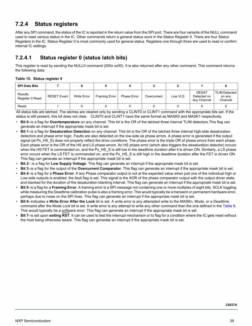
7.2.4 Status registersAfter any SPI command, the status of the IC is reported in the return value from the SPI port. There are four variants of the NULL command used to read various status in the IC. Other commands return a general status word in the Status Register 0. There are four Status Registers in the IC. Status Register 0 is most commonly used for general status. Registers one through three are used to read or confirm internal IC settings.
7.2.4.1 Status register 0 (status latch bits)
This register is read by sending the NULL0 command (000x xx00). It is also returned after any other command. This command returns the following data: Table 15. Status register 0
SPI Data Bits 7 6 5 4 3 2 1 0
Results Register 0 Read
RESET Event Write Error Framing Error Phase Error Overcurrent Low VLSDESAT
Detected on any Channel
TLIM Detected on any
Channel
Reset 1 0 0 0 0 0 0 0
All status bits are latched. The latches are cleared only by sending a CLINT0 or CLINT1 command with the appropriate bits set. If the status is still present, this bit does not clear. CLINT0 and CLINT1 have the same format as MASK0 and MASK1 respectively.
• Bit 0–is a flag for Overtemperature on any channel. This bit is the OR of the latched three internal TLIM detectors.This flag can generate an interrupt if the appropriate mask bit is set.
• Bit 1–is a flag for Desaturation Detection on any channel. This bit is the OR of the latched three internal high-side desaturation detectors and phase error logic. Faults are also detected on the low-side as phase errors. A phase error is generated if the output signal (at Px_HS_S) does not properly reflect the drive conditions. The phase error is the triple OR of phase errors from each phase. Each phase error is the OR of the HS and LS phase errors. An HS phase error (which also triggers the desaturation detector) occurs when the HS FET is commanded on, and the Px_HS_S is still low in the deadtime duration after it is driven ON. Similarly, a LS phase error occurs when the LS FET is commanded on, and the Px_HS_S is still high in the deadtime duration after the FET is driven ON. This flag can generate an interrupt if the appropriate mask bit is set.
• Bit 2– is a flag for Low Supply Voltage. This flag can generate an interrupt if the appropriate mask bit is set. • Bit 3–is a flag for the output of the Overcurrent Comparator. This flag can generate an interrupt if the appropriate mask bit is set. • Bit 4–is a flag for a Phase Error. If any Phase comparator output is not at the expected value when just one of the individual high or
Low-side outputs is enabled, the fault flag is set. This signal is the XOR of the phase comparator output with the output driver state, and blanked for the duration of the desaturation blanking interval. This flag can generate an interrupt if the appropriate mask bit is set.
• Bit 5–is a flag for a Framing Error. A framing error is a SPI message not containing one or more multiples of eight bits. SCLK toggling while measuring the Deadtime calibration pulse is also a framing error. This would typically be a transient or permanent hardware error, perhaps due to noise on the SPI lines. This flag can generate an interrupt if the appropriate mask bit is set.
• Bit 6–indicates a Write Error After the Lock bit is set. A write error is any attempted write to the MASKn, Mode, or a Deadtime command after the Mode Lock bit is set. A write error is any attempt to write any other command than the one defined in the Table 8. This would typically be a software error. This flag can generate an interrupt if the appropriate mask bit is set.
• Bit 7–is set upon exiting RST. It can be used to test the interrupt mechanism or to flag for a condition where the IC gets reset without the host being otherwise aware. This flag can generate an interrupt if the appropriate mask bit is set.
NXP Semiconductors 39
33937A
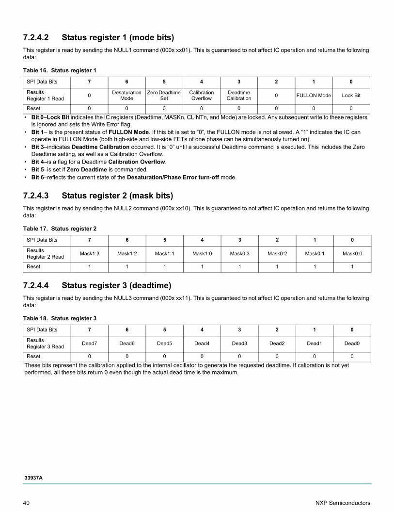
7.2.4.2 Status register 1 (mode bits)
This register is read by sending the NULL1 command (000x xx01). This is guaranteed to not affect IC operation and returns the following data:
7.2.4.3 Status register 2 (mask bits)
This register is read by sending the NULL2 command (000x xx10). This is guaranteed to not affect IC operation and returns the following data:
7.2.4.4 Status register 3 (deadtime)
This register is read by sending the NULL3 command (000x xx11). This is guaranteed to not affect IC operation and returns the following data:
Table 16. Status register 1
SPI Data Bits 7 6 5 4 3 2 1 0
Results Register 1 Read
0Desaturation
ModeZero Deadtime
SetCalibration Overflow
Deadtime Calibration
0 FULLON Mode Lock Bit
Reset 0 0 0 0 0 0 0 0
• Bit 0–Lock Bit indicates the IC registers (Deadtime, MASKn, CLINTn, and Mode) are locked. Any subsequent write to these registers is ignored and sets the Write Error flag.
• Bit 1– is the present status of FULLON Mode. If this bit is set to “0”, the FULLON mode is not allowed. A “1” indicates the IC can operate in FULLON Mode (both high-side and low-side FETs of one phase can be simultaneously turned on).
• Bit 3–indicates Deadtime Calibration occurred. It is “0” until a successful Deadtime command is executed. This includes the Zero Deadtime setting, as well as a Calibration Overflow.
• Bit 4–is a flag for a Deadtime Calibration Overflow.• Bit 5–is set if Zero Deadtime is commanded.• Bit 6–reflects the current state of the Desaturation/Phase Error turn-off mode.
Table 17. Status register 2
SPI Data Bits 7 6 5 4 3 2 1 0
Results Register 2 Read
Mask1:3 Mask1:2 Mask1:1 Mask1:0 Mask0:3 Mask0:2 Mask0:1 Mask0:0
Reset 1 1 1 1 1 1 1 1
Table 18. Status register 3
SPI Data Bits 7 6 5 4 3 2 1 0
Results Register 3 Read
Dead7 Dead6 Dead5 Dead4 Dead3 Dead2 Dead1 Dead0
Reset 0 0 0 0 0 0 0 0
These bits represent the calibration applied to the internal oscillator to generate the requested deadtime. If calibration is not yet performed, all these bits return 0 even though the actual dead time is the maximum.
40 NXP Semiconductors
33937A
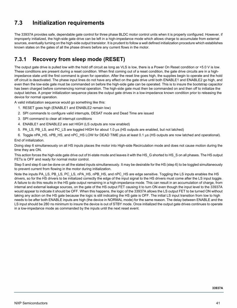
7.3 Initialization requirements
The 33937A provides safe, dependable gate control for three phase BLDC motor control units when it is properly configured. However, if improperly initialized, the high-side gate drive can be left in a high-impedance mode which allows charge to accumulate from external sources, eventually turning on the high-side output transistor. It is prudent to follow a well defined initialization procedure which establishes known states on the gates of all the phase drivers before any current flows in the motor.
7.3.1 Recovery from sleep mode (RESET)The output gate drive is pulled low with the hold off circuit as long as VLS is low, there is a Power On Reset condition or +5.0 V is low. These conditions are present during a reset condition. When first coming out of a reset condition, the gate drive circuits are in a high-impedance state until the first command is given for operation. After the reset line goes high, the supplies begin to operate and the hold off circuit is deactivated. The phase input lines do not have any effect on the gate drive until both ENABLE1 and ENABLE2 go high, and even then the low-side gate must be commanded on before the high-side gate can be operated. This is to insure the bootstrap capacitor has been charged before commencing normal operation. The high-side gate must then be commanded on and then off to initialize the output latches. A proper initialization sequence places the output gate drives in a low-impedance known condition prior to releasing the device for normal operation.
A valid initialization sequence would go something like this:
1. RESET goes high (ENABLE1 and ENABLE2 remain low)
2. SPI commands to configure valid interrupts, DESAT mode and Dead Time are issued
3. SPI command to clear all interrupt conditions
4. ENABLE1 and ENABLE2 are set HIGH (LS outputs are now enabled)
5. PA_LS, PB_LS, and PC_LS are toggled HIGH for about 1.0 μs (HS outputs are enabled, but not latched)
6. Toggle nPA_HS, nPB_HS, and nPC_HS LOW for DEAD TIME plus at least 0.1 μs (HS outputs are now latched and operational).
End of initialization.
Doing step 6 simultaneously on all HS inputs places the motor into High-side Recirculation mode and does not cause motion during the time they are ON.
This action forces the high-side gate drive out of tri-state mode and leaves it with the HS_G shorted to HS_S on all phases. The HS output FETs is OFF and ready for normal motor control.
Step 5 and step 6 can be done on all the stated inputs simultaneously. It may be desirable for the HS (step 6) to be toggled simultaneously to prevent current from flowing in the motor during initialization.
Note the inputs PA_LS, PB_LS, PC_LS, nPA_HS, nPB_HS, and nPC_HS are edge sensitive. Toggling the LS inputs enables the HS drivers, so for the HS drivers to be initialized correctly the edge of the input signal to the HS drivers must come after the LS input toggle. A failure to do this results in the HS gate output remaining in a high-impedance mode. This can result in an accumulation of charge, from internal and external leakage sources, on the gate of the HS output FET causing it to turn ON even though the input level to the 33937A would appear to indicate it should be OFF. When this happens, the logic of the 33937A allows the LS output FET to be turned ON without taking any action on the HS gate because the logic is still indicating the HS gate is OFF. The initial LS input transition from low to high needs to be after both ENABLE inputs are high (the device in NORMAL mode) for the same reason. The delay between ENABLE and the LS input should be 280 ns minimum to insure the device is out of STBY mode. Once initialized the output gate drives continues to operate in a low-impedance mode as commanded by the inputs until the next reset event.
NXP Semiconductors 41
33937A
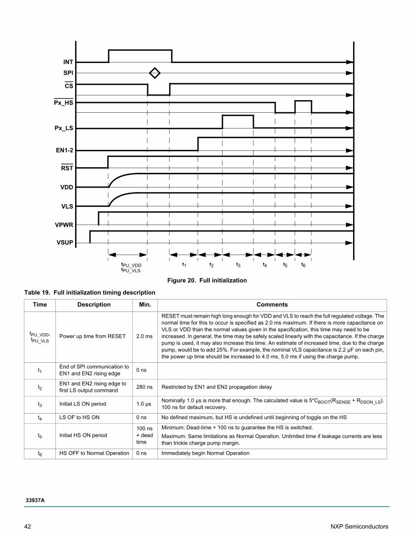
Figure 20. Full initialization
Table 19. Full initialization timing description
Time Description Min. Comments
tPU_VDD, tPU_VLS
Power up time from RESET 2.0 ms
RESET must remain high long enough for VDD and VLS to reach the full regulated voltage. The normal time for this to occur is specified as 2.0 ms maximum. If there is more capacitance on VLS or VDD than the normal values given in the specification, this time may need to be increased. In general, the time may be safely scaled linearly with the capacitance. If the charge pump is used, it may also increase this time. An estimate of increased time, due to the charge pump, would be to add 25%. For example, the nominal VLS capacitance is 2.2 µF on each pin, the power up time should be increased to 4.0 ms, 5.0 ms if using the charge pump.
t1End of SPI communication to EN1 and EN2 rising edge
0 ns
t2EN1 and EN2 rising edge to first LS output command
280 ns Restricted by EN1 and EN2 propagation delay
t3 Initial LS ON period 1.0 µsNominally 1.0 µs is more that enough. The calculated value is 5*CBOOT(RSENSE + RDSON_LS). 100 ns for default recovery.
t4 LS OF to HS ON 0 ns No defined maximum, but HS is undefined until beginning of toggle on the HS
t5 Initial HS ON period100 ns + dead time
Minimum: Dead-time + 100 ns to guarantee the HS is switched.
Maximum: Same limitations as Normal Operation. Unlimited time if leakage currents are less than trickle charge pump margin.
t6 HS OFF to Normal Operation 0 ns Immediately begin Normal Operation
INT
SPI
CS
Px_HS
Px_LS
EN1-2
RST
VDD
VLS
VPWR
VSUP
tPU_VDDtPU_VLS
t1 t2 t4 t5 t6t3
42 NXP Semiconductors
33937A
7.3.2 Recovery from standby mode or a faultWhen the 33937A is placed in Standby mode or a fault condition causes a shutdown, the Gate outputs are all driven low. The high-side gate drive is then disabled and locked to prevent unauthorized transitions. This requires an initialization sequence to recover normal operation at the end of this mode of operation. The initialization sequence is nearly identical to recovery from Sleep mode, with the modification that the initial pulse to the low-side control inputs can be reduced to a 100 ns pulse (the low-side gates may not actually change state). The initialization is then completed by cycling the high-side gates to re-engage the gate drive and insure that it is in the proper state prior to resuming normal operation.
A valid initialization sequence would go something like this:
1. SPI command to clear all interrupt conditions
2. ENABLE1 and ENABLE2 are set HIGH (LS outputs are now enabled)
3. PA_LS, PB_LS and PC_LS are toggled HIGH for at least 100 ns (HS gate drive outputs are enabled) longer if bootstrap capacitors need charged.
4. Toggle nPA_HS, nPB_HS and nPC_HS LOW for DEAD TIME plus at least 100 ns.
End of initialization.
Doing step 4 simultaneously on all HS inputs places the motor into High-side Recirculation mode and does not cause motion during the time they are ON.
This action restores the high-side gate drive operation and leave it with the HS_G shorted to HS_S on all phases. The HS output FETs will be OFF and ready for normal motor control.
Step 3 and step 4 can be done on all the stated inputs simultaneously. In fact it is desirable for the HS (step 4) to be toggled simultaneously to prevent current from flowing in the motor during initialization.
Note the inputs PA_LS, PB_LS, PC_LS, nPA_HS, nPB_HS, and nPC_HS are edge sensitive. Toggling the LS inputs enables the HS drivers, so for the HS drivers to be initialized correctly, the edge of the input signal to the HS drivers must come after the LS input toggle. A failure to do this results in the HS gate output remaining locked out from input control. The initial LS input transition from low to high needs to be after both ENABLE inputs are high (the device in Normal mode) for the same reason. The delay between ENABLE and the LS input should be 280 ns minimum to insure the device is out of STBY mode.
Figure 21. Recovery initialization
The horizontal divisions are not to scale. They are a reference to show the sequence of operation. Either individual nPx_HS and Px_LS or nPx_Combined may be used. nPx_Combined is defined as both nPx_HS and Px_LS tied together or operated to the same logic level simultaneously.
INT
SPI
nCS
Px_Combined
nPx_HS
Px_LS
EN2
EN1
Clear
0.1µs
0.1µs
NXP Semiconductors 43
33937A
7.3.3 IC initializationThis process flow initializes the IC and its software environment.
1. Apply power (VSYS) to module
2. Remove RST (RST goes high, EN1 and EN2 are still low)a) When RST rises above the threshold, the device powers up. The charge pump (if configured) starts and allows VDD and VLS to
stabilize.
2. Initialize registersa) Clear all interrupt status flags (send CINT0 and CINT1)
b) Initialize MASK register by sending 0010 xxxx or 0011 xxxx to mask out unwanted interrupts.c) Set desired dead time either by commanding zero dead time or calibrating the dead time.d) Send MODE command with desired bits, and also the Lock bit. e.g. 01000001. This prevents further mode changes.
5. Bring EN1 & EN2 high
6. Initialize the outputsa) Command all Px_HS to logic 1 (High-side OFF)
b) Command all Px_LS to logic 1 (commanding Low-side ON). The input must transition from low to high after EN1 and EN2 have gone high.
c) Wait for the bootstrap capacitors to charge (about 1.0 μs typically)d) Command all Px_LS to logic 0 (command low-side OFF)e) Command all Px_HS to logic 0 (command high-side ON)f) Command all Px_HS to logic 1 (command high-side OFF)
The device is now ready for normal operation.
7.3.4 Interrupt handlerWhen an interrupt occurs, the general procedure is to send NULL0 and NULL1 commands to determine what happened, take corrective
action (if needed), clear the fault, and return. Because the return value from an SPI command is actually returned in the subsequent message, main-loop software trying to read SR1, SR2, or SR3, may experience an interrupt between sending the SPI command and the subsequent read. Thus if these registers are to be read, special care must be taken in the software to ensure the correct results are being interpreted.
44 NXP Semiconductors
33937A
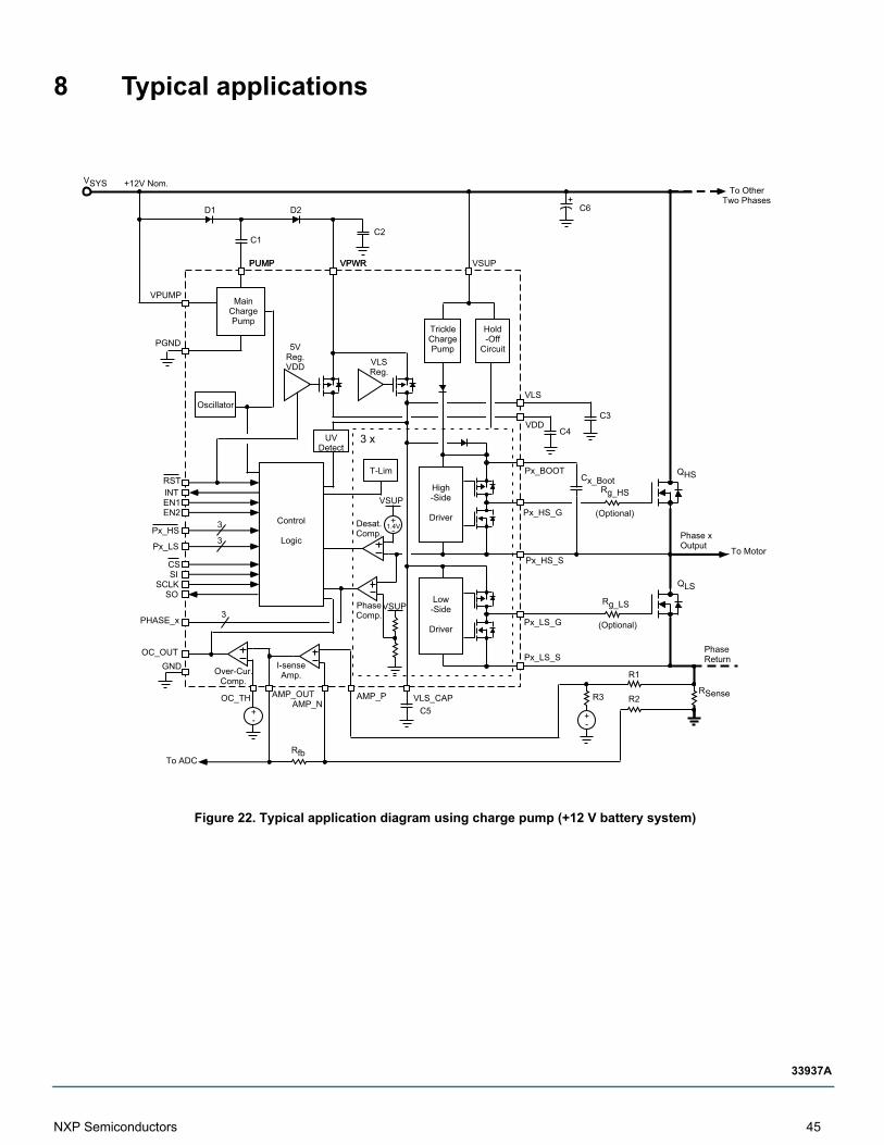
8 Typical applications
Figure 22. Typical application diagram using charge pump (+12 V battery system)
VSUPVPWRPUMP
VPUMP
PGND
MainChargePump
Oscillator
UVDetect
5VReg.VDD
Control
Logic
T-LimRST
EN1EN2
INT
Px_HS
Px_LS
3
3
CSSI
SCLKSO
PHASE_x3
OC_OUT
OC_TH AMP_OUTAMP_N
AMP_P VLS_CAP
Px_LS_S
Px_LS_G
Px_HS_G
Px_HS_S
Px_BOOT
VDD
VLS
TrickleChargePump
Hold-Off
Circuit
High-Side
Driver
Low-Side
Driver
VLSReg.
I-senseAmp.Over-Cur.
Comp.
PhaseComp.
Desat.Comp.
To Motor
3 x
+-
+-
VSYS
+-
VSUP
VSUP
1.4V
GND
To OtherTwo Phases
+12V Nom.
Phase xOutput
To ADC
Rg_HS
Rg_LS
(Optional)
(Optional)
Cx_Boot
RSense
PhaseReturn
VPWRPUMP
D1 D2
C1C2
C6
C3
C5
C4
R1
R2R3
Rfb
QHS
QLS
NXP Semiconductors 45
33937A
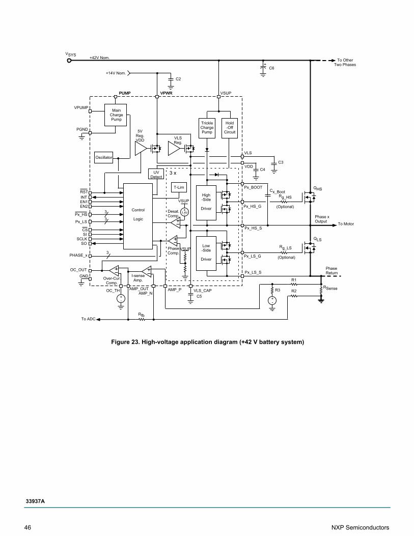
Figure 23. High-voltage application diagram (+42 V battery system)
VSUPVPWRPUMP
VPUMP
PGND
MainChargePump
Oscillator
UVDetect
5VReg.VDD
Control
Logic
T-LimRST
EN1EN2
INT
Px_HS
Px_LS
3
3
CSSI
SCLKSO
PHASE_x3
OC_OUT
OC_TH AMP_OUTAMP_N
AMP_P VLS_CAP
Px_LS_S
Px_LS_G
Px_HS_G
Px_HS_S
Px_BOOT
VDD
VLS
TrickleChargePump
Hold-Off
Circuit
High-Side
Driver
Low-Side
Driver
VLSReg.
I-senseAmp.Over-Cur.
Comp.
PhaseComp.
Desat.Comp.
To Motor
3 x
+-
+-
VSYS
+-
VSUP
VSUP
1.4V
GND
To OtherTwo Phases
Phase xOutput
To ADC
Rg_HS
Rg_LS
(Optional)
(Optional)
Cx_Boot
RSense
PhaseReturn
VPWRPUMP
C2
C6
C3
C5
C4
R1
R2R3
Rfb
QHS
QLS
+42V Nom.
+14V Nom.
46 NXP Semiconductors
33937A
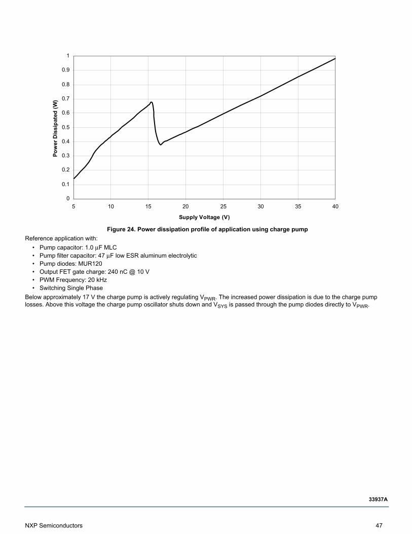
Figure 24. Power dissipation profile of application using charge pump
Reference application with:
• Pump capacitor: 1.0 μF MLC• Pump filter capacitor: 47 μF low ESR aluminum electrolytic• Pump diodes: MUR120• Output FET gate charge: 240 nC @ 10 V• PWM Frequency: 20 kHz• Switching Single Phase
Below approximately 17 V the charge pump is actively regulating VPWR. The increased power dissipation is due to the charge pump losses. Above this voltage the charge pump oscillator shuts down and VSYS is passed through the pump diodes directly to VPWR.
0
0.1
0.2
0.3
0.4
0.5
0.6
0.7
0.8
0.9
1
5 10 15 20 25 30 35 40
Supply Voltage (V)
Po
wer
Dis
sip
ated
(W
)
NXP Semiconductors 47
33937A
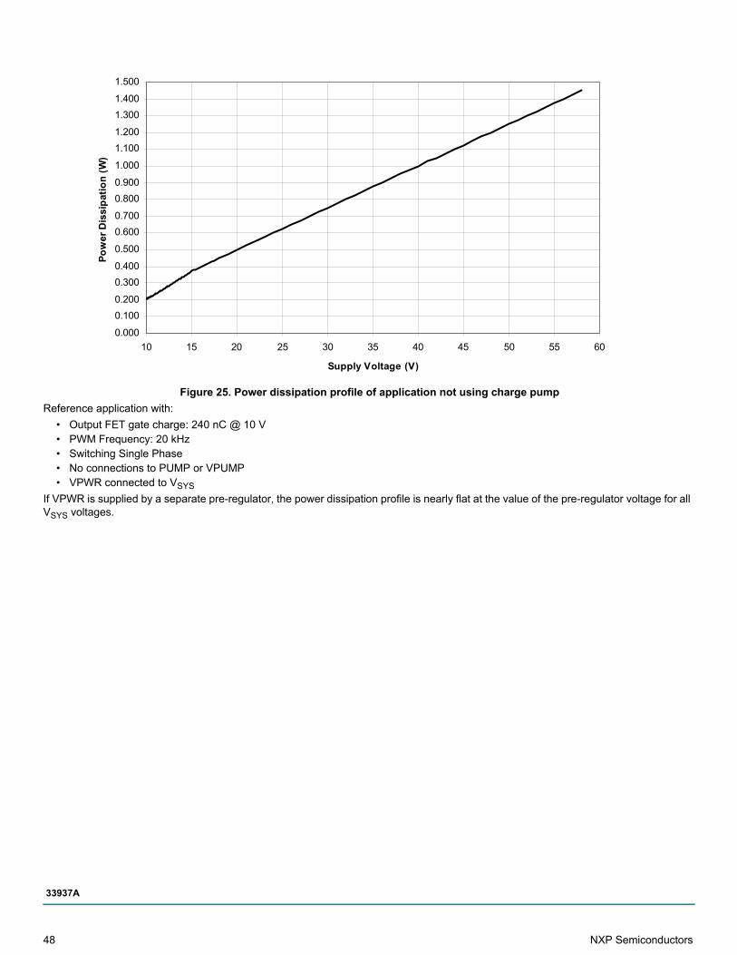
Figure 25. Power dissipation profile of application not using charge pump
Reference application with:
• Output FET gate charge: 240 nC @ 10 V• PWM Frequency: 20 kHz• Switching Single Phase• No connections to PUMP or VPUMP• VPWR connected to VSYS
If VPWR is supplied by a separate pre-regulator, the power dissipation profile is nearly flat at the value of the pre-regulator voltage for all VSYS voltages.
0.000
0.100
0.200
0.300
0.400
0.500
0.600
0.700
0.800
0.900
1.000
1.100
1.200
1.300
1.400
1.500
10 15 20 25 30 35 40 45 50 55 60
Supply Voltage (V)
Po
wer
Dis
sip
atio
n (
W)
48 NXP Semiconductors
33937A
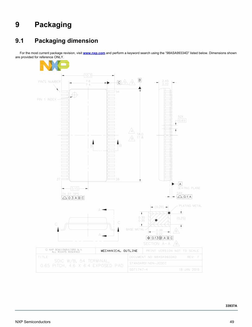
9 Packaging
9.1 Packaging dimension
For the most current package revision, visit www.nxp.com and perform a keyword search using the “98ASA99334D” listed below. Dimensions shown are provided for reference ONLY.
NXP Semiconductors 49
33937A
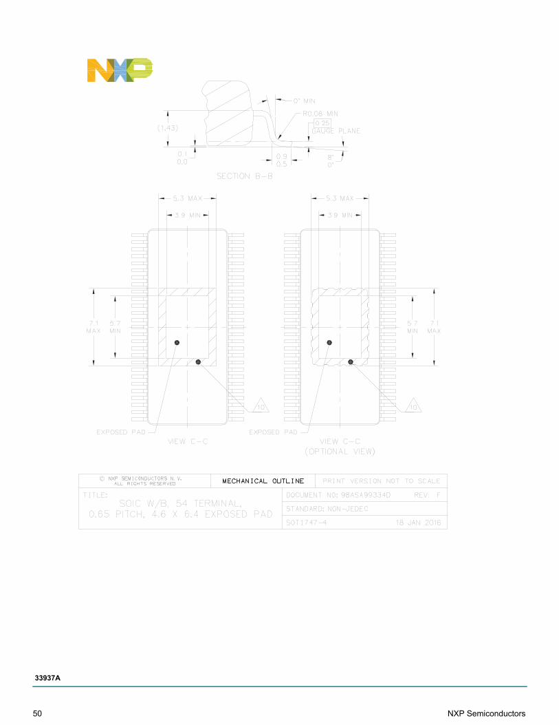
50 NXP Semiconductors
33937A
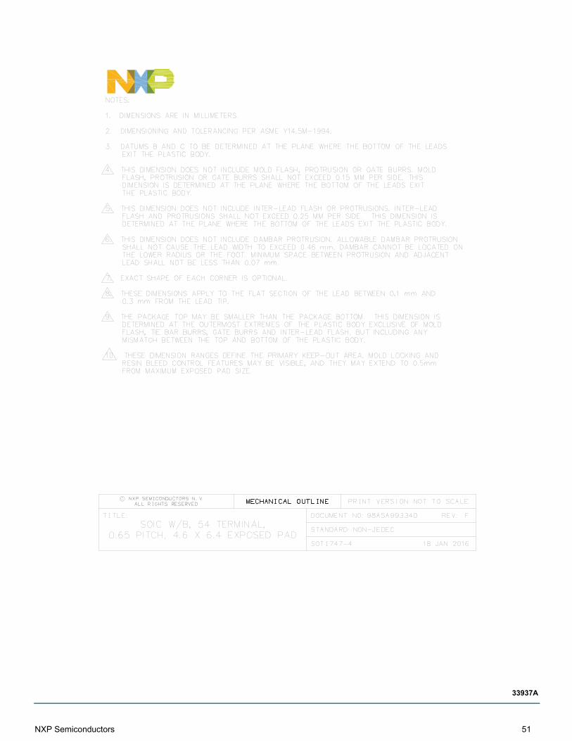
NXP Semiconductors 51
33937A
10 Revision history
Revision Date Description of Changes
1.0 6/2008 • Initial Release
2.0 7/2008
• Updated specifications for current sense amplifier and overcurrent comparator• Added Gain/Phase curves for current sense amplifier• Added typical curves for load margin on Px_CBOOT• Added discussion about bootstrap capacitors and requirements for external bootstrap diodes• Updated application drawings• Added VSUP requirement for hold-off
3.0 11/2008
• Updated NXP form and style• Added note to VLS Regulator Outputs (VLS, VLS_CAP)• Changed Charge Device Model - CDM• Corrected title to No output loads on Gate Drive Pins, No PWM, Outputs initialized• Changed In order to achieve a 100% duty cycle operation of the high-side external FETs, a fully integrated trickle
charge pump provides the charge necessary to maintain the external FET gates at fully enhanced levels. The trickle charge pump has limited ability to supply external leakage paths while performing it’s primary function. The graph in Figure 11 shows the typical margin for supplying external current loads. These limits are based on maintaining the voltage at CBOOT at least 3.0 V greater than the voltage on the HS_S for that phase. If this voltage differential becomes less than 3.0 V, the corresponding high-side FET most likely does not remain fully enhanced and the high-side driver may malfunction due to insufficient bias voltage between CBOOT and HS_S. and associated paragraphs
4.0 12/2008
• Added PCZ33937AEK/R2 Part number throughout.• Added Note and changed parameters for Desaturation Detector and Phase Comparator to Dynamic Electrical
Characteristics Table.• Replaced Typical Application Diagrams (Pages 40 and 41).• Page 10 remove VDD Threshold (VDD Falling) change note 23
5.0 4/2009 • Note 41 clarification.
6.0 9/2009 • Changed part number from PCZ33937A to MCZ33937A on page 1. Added Device Variation table on page 2.
7.0 3/2011 • Revised per Specific customer requirements (not published)
8.0 8/2012• Removed part number MCZ33937AEK and replaced with part number MC33937APEK.• Removed part number MCZ33937EK/R2 and specific differences. Noted in ordering information to see
specification MC33937 Rev 6.0 for obsolete parts.
9.011/2015
• Clarified Gate Capability feature on page 1.• Updated NXP form and style.
7/2016 • Updated to NXP document form and style
52 NXP Semiconductors
33937A
Information in this document is provided solely to enable system and software implementers to use NXP products.
There are no expressed or implied copyright licenses granted hereunder to design or fabricate any integrated circuits
based on the information in this document. NXP reserves the right to make changes without further notice to any
products herein.
NXP makes no warranty, representation, or guarantee regarding the suitability of its products for any particular
purpose, nor does NXP assume any liability arising out of the application or use of any product or circuit, and
specifically disclaims any and all liability, including without limitation, consequential or incidental damages. "Typical"
parameters that may be provided in NXP data sheets and/or specifications can and do vary in different applications,
and actual performance may vary over time. All operating parameters, including "typicals," must be validated for each
customer application by the customer's technical experts. NXP does not convey any license under its patent rights nor
the rights of others. NXP sells products pursuant to standard terms and conditions of sale, which can be found at the
following address:
http://www.nxp.com/terms-of-use.html.
How to Reach Us:Home Page: NXP.com
Web Support: http://www.nxp.com/support
NXP, the NXP logo, Freescale, the Freescale logo and SMARTMOS are trademarks of NXP B.V. All other product or
service names are the property of their respective owners. All rights reserved.
© 2016 NXP B.V.
Document Number: MC33937Rev. 9.0
7/2016
Top Related