


Languages
Pages
Legal


MAX1870A Step-Up/Step-Down Li+ Battery Charger
EVALUATION KIT AVAILABLE
General DescriptionThe MAX1870A step-up/step-down multichemistrybattery charger charges with battery voltages aboveand below the adapter voltage. This highly integratedcharger requires a minimum number of external com-ponents. The MAX1870A uses a proprietary step-up/step-down control scheme that provides efficientcharging. Analog inputs control charge current andvoltage, and can be programmed by the host or hardwired.
The MAX1870A accurately charges two to four lithium-ion (Li+) series cells at greater than 4A. A program-mable input current limit is included, which avoidsoverloading the AC adapter when supplying the loadand the battery charger simultaneously. This reducesthe maximum adapter current, which reduces cost. TheMAX1870A provides analog outputs to monitor the cur-rent drawn from the AC adapter and charge current. A digital output indicates the presence of an ACadapter. When the adapter is removed, the MAX1870Aconsumes less than 1µA from the battery.
The MAX1870A is available in a 32-pin thin QFN (5mm x 5mm) package and is specified over the -40°C to +85°C extended temperature range. TheMAX1870A evaluation kit (MAX1870AEVKIT) is avaiable to help reduce design time.
ApplicationsNotebook and Subnotebook Computers
Handheld Terminals
Benefits and Features• Highly Flexible Input Voltage Range Works with
Affordable AC Adapters
• Step-Up/Step-Down Control Scheme
• Input Voltage from 8V to 28V
• Analog Output Indicates Adapter Current
• Accurately Charge Li+ or NiCd/NiMH Batteries
• Battery Voltage from 0 to 17.6V
• ±0.5% Charge-Voltage Accuracy
• ±9% Charge-Current Accuracy
• ±8% Input Current-Limit Accuracy
• Tune Design to Increase Safety and Efficiency
• Programmable Maximum Battery Charge Current
• Analog Inputs Control Charge Current, Charge
Voltage, and Input Current Limit
• 32-Pin Thin QFN (5mm x 5mm) Package Saves
Space While Supporting Step-Up and Step-Down
Operation
Ordering Information
MAX1870A
REFIN
DCIN
CSSP
CSSN
DHI
DBSTCSIPCSIN
BATT
SHDN
ASNS
VCTL
IINP
PGND
SYSTEMLOAD
N
P
GND
ICTL
CLS
CELLS
FROM WALL ADAPTER
CSSS
VHN
VHP
BLKP
REF
LDO
DLOV
Typical Operating Circuit
Pin Configuration appears at end of data sheet.
PART TEMP RANGE PIN-PACKAGE
MAX1870AETJ -40°C to +85°C 32 Thin QFN
MAX1870AETJ+ -40°C to +85°C 32 Thin QFN
+Denotes a lead(Pb)-free/RoHS-compliant package.
19-3243; Rev 3; 8/15
MAX1870A Step-Up/Step-Down Li+ Battery Charger
Maxim Integrated | 2www.maximintegrated.com
Absolute Maximum Ratings
Stresses beyond those listed under “Absolute Maximum Ratings” may cause permanent damage to the device. These are stress ratings only, and functionaloperation of the device at these or any other conditions beyond those indicated in the operational sections of the specifications is not implied. Exposure toabsolute maximum rating conditions for extended periods may affect device reliability.
DCIN, CSSP, CSSS, CSSN, VHP, VHN, DHI to GND......................................-0.3V to +30V
VHP, DHI to VHN .....................................................-0.3V to +6VBATT, CSIP, CSIN, BLKP to GND ..........................-0.3V to +20VCSIP to CSIN, CSSP to CSSN,
CSSP to CSSS, PGND to GND..........................-0.3V to +0.3VCCI, CCS, CCV, REF, IINP to GND ..........-0.3V to (VLDO + 0.3V)DBST to GND..........................................-0.3V to (VDLOV + 0.3V)DLOV, VCTL, ICTL, REFIN, CELLS,
CLS, LDO, ASNS, SHDN to GND.........................-0.3V to +6V
LDO Current........................................................................50mAContinuous Power Dissipation (TA = +70°C)
32-Pin Thin QFN 5mm x 5mm (derate 21mW/°C above +70°C)......................................1.7W
Operating Temperature RangeMAX1870AETJ.................................................-40°C to +85°C
Storage Temperature Range .............................-60°C to +150°CLead Temperature (soldering, 10s) ................................ +300°C
Electrical Characteristics(Circuit of Figure 2, VDCIN = VCSSP = VCSSN = VCSSS = VVHP = 18V, VBATT = VCSIP = VCSIN = VBLKP = 12V, VREFIN = 3.0V, VICTL =0.75 x VREFIN, VCTL = LDO, CELLS = FLOAT, GND = PGND = 0, VDLOV = 5.4V, TA = 0°C to +85°C, unless otherwise noted. Typicalvalues are at TA = +25°C.)
PARAMETER CONDITIONS MIN TYP MAX UNITS
CHARGE-VOLTAGE REGULATION VCTL Range 0 3.6 V
VVCTL = VLDO (2 cells) -0.5 +0.5
VVCTL = VLDO (3 cells) -0.5 +0.5
VVCTL = VLDO (4 cells) -0.5 +0.5
VVCTL = VREFIN (2 cells) -0.8 +0.8
VVCTL = VREFIN (3 cells) -0.8 +0.8
VVCTL = VREFIN (4 cells) -0.8 +0.8
VVCTL = VREFIN / 20 (2 cells) -1.2 +1.2
VVCTL = VREFIN / 20 (3 cells) -1.2 +1.2
Battery Regulation VoltageAccuracy
VVCTL = VREFIN / 20 (4 cells) -1.2 +1.2
%
VCTL Default Threshold VCTL rising 4.0 4.1 4.2 V 0 < VVCTL < VREFIN -1 +1
DCIN = 0, VREFIN = VVCTL = 3.6V -1 +1 VCTL Input Bias Current
VCTL = DCIN = 0, VREFIN = 3.6V -1 +1
µA
CHARGE-CURRENT REGULATION ICTL Range 0 3.6 V
VICTL = VREFIN 67 73 79
VICTL = VREFIN x 0.8 54 59 64 Quick-Charge-Current Accuracy
VICTL = VREFIN x 0.583 39 43 47
mV
Trickle-Charge-Current Accuracy VICTL = VREFIN x 0.0625 3.0 4.5 6.0 mV
BATT/CSIP/CSIN Input VoltageRange
0 19 V
DCIN = 0 0.1 2 ICTL = 0 0.1 2 CSIP Input Current
ICTL = REFIN 350 600
µA

MAX1870A Step-Up/Step-Down Li+ Battery Charger
Maxim Integrated | 3www.maximintegrated.com
PARAMETER CONDITIONS MIN TYP MAX UNITS
DCIN = 0 0.1 2 ICTL = 0 0.1 2 CSIN Input Current
ICTL = REFIN 0.1 2 µA
ICTL Power-Down-ModeThreshold Voltage
REFIN /100
REFIN /55
REFIN /32
V
0 < VICTL < VREFIN -1 +1 ICTL Input Bias Current ICTL = DCIN = 0, VREFIN = 3.6V -1 +1
µA
INPUT-CURRENT REGULATION CLS = REF 97 105 113 Charger-Input Current-Limit
Accuracy (VCSSP - VCSSN) CSSS = CSSP
CLS = REF x 0.845 81 88 95 mV
CLS = REF 97 105 113 System-Input Current-LimitAccuracy (VCSSP - VCSSS)
CSSN = CSSP CLS = REF x 0.845 81 88 95
mV
CSSP/CSSS/CSSN Input VoltageRange
8 28 V
VCSSP = VCSSN = VCSSS = VDCIN = 6V -1 +1 CSSP Input Current VCSSP = VCSSN = VCSSS = VDCIN = 8V, 28V 700 1200
µA
VCSSP = VCSSN = VCSSS = VDCIN = 6V -1 +1 CSSS/CSSN Input Current VCSSP = VCSSN = VCSSS = VDCIN = 8V, 28V -1 +1
µA
CLS Input Range VREF / 2 VREF V CLS Input Bias Current CLS = REF -1 +1 µA
IINP Transconductance VCSSP - VCSSS = 102mV, CSSN = CSSP 2.5 2.8 3.1 µA/mV
VCSSP - VCSSN = 200mV, VIINP = 0V 350 IINP Output Current VCSSP - VCSSS = 200mV, VIINP = 0V 350
µA
VCSSP - VCSSN = 200mV, IINP float 3.5 IINP Output Voltage VCSSP - VCSSS = 200mV, IINP float 3.5
V
SUPPLY AND LINEAR REGULATOR DCIN Input Voltage Range 8 28 V
DCIN falling 4 6.2 DCIN Undervoltage Lockout DCIN rising 6.3 7.85
V
DCIN Quiescent Current 8.0V < VDCIN < 28V 3.5 6 mA
BATT Input Voltage Range 0 19 V DCIN = 0 0.1 1 BATT Input Bias Current VBATT = 2V to 19V 300 500
µA
LDO Output Voltage No load 5.3 5.4 5.5 V LDO Load Regulation 0 < ILDO < 10mA 70 150 mV
LDO Undervoltage Lockout VDCIN = 8V, LDO rising 4.00 5.0 5.25 V
Electrical Characteristics (continued)(Circuit of Figure 2, VDCIN = VCSSP = VCSSN = VCSSS = VVHP = 18V, VBATT = VCSIP = VCSIN = VBLKP = 12V, VREFIN = 3.0V, VICTL =0.75 x VREFIN, VCTL = LDO, CELLS = FLOAT, GND = PGND = 0, VDLOV = 5.4V, TA = 0°C to +85°C, unless otherwise noted. Typicalvalues are at TA = +25°C.)

MAX1870A Step-Up/Step-Down Li+ Battery Charger
Maxim Integrated | 4www.maximintegrated.com
PARAMETER CONDITIONS MIN TYP MAX UNITS
REFERENCE REF Output Voltage IREF = 0µA 4.076 4.096 4.116 V REF Load Regulation 0 < IREF < 500µA 5 10 mV
REF Undervoltage-Lockout TripPoint
VREF falling 3.1 3.9 V
REFIN Input Range 2.5 3.6 V REFIN UVLO Rising 1.9 2.2 V REFIN UVLO Hysteresis 50 mV
VDCIN = 18V 50 100 REFIN Input Bias Current DCIN = 0, VREFIN = 3.6V -1 +1 µA
SWITCHING REGULATOR C ycl e- b y- C ycl e S tep - U p M axi m um C ur r ent- Li m i t S ense V ol tag e
VDCIN = 12V, VBATT = 16.8V 135 150 165 mV
C ycl e- b y- C ycl e S tep - D ow nM axi m um C ur r ent- Li m i t S enseV ol tag e
VDCIN = 19V, VBATT = 16.8V 135 150 165 mV
Step-Down On-Time VDCIN = 18V, VBATT = 16.8V 2.2 2.4 2.6 µs
Minimum Step-Down Off-Time VDCIN = 18V, VBATT = 16.8V 0.15 0.4 0.50 µs
Step-Up Off-Time VDCIN = 12V, VBATT = 16.8V 1.6 1.8 2.0 µs
Minimum Step-Up On-Time VDCIN = 12V, VBATT = 16.8V 0.15 0.3 0.40 µs
MOSFET DRIVERS VHP - VHN Output Voltage 8V < VVHP < 28V, no load 4.5 5 5.5 V VHN Load Regulation 0 < IVHN < 10mA 70 150 mV
DHI On-Resistance High ISOURCE = 10mA 2 5 Ω DHI On-Resistance Low ISINK = 10mA 1 3 Ω
DCIN = 0 0.1 1 µA VHP Input Bias Current VDCIN = 18V 1.3 2 mA
ICTL = 0 0.1 2 BLKP Input Bias Current VICTL = VREFIN = 3.3V 100 400 µA
DLOV Supply Current DBST low 5 10 µA
DBST On-Resistance High ISOURCE = 10mA 2 5 Ω DBST On-Resistance Low ISINK = 10mA 1 3 Ω ERROR AMPLIFIERS GMV Amplifier LoopTransconductance
V C TL = RE FIN , V BAT T = 16.8V 0.05 0.1 0.20 µA/mV
GMI Amplifier LoopTransconductance
ICTL = REFIN, VCSIP - VCSIN = 72mV 1.8 2.4 3.0 µA/mV
Electrical Characteristics (continued)(Circuit of Figure 2, VDCIN = VCSSP = VCSSN = VCSSS = VVHP = 18V, VBATT = VCSIP = VCSIN = VBLKP = 12V, VREFIN = 3.0V, VICTL =0.75 x VREFIN, VCTL = LDO, CELLS = FLOAT, GND = PGND = 0, VDLOV = 5.4V, TA = 0°C to +85°C, unless otherwise noted. Typicalvalues are at TA = +25°C.)
MAX1870A Step-Up/Step-Down Li+ Battery Charger
Maxim Integrated | 5www.maximintegrated.com
PARAMETER CONDITIONS MIN TYP MAX UNITS
VCLS = REF, VCSSP - VCSSN = 102mV, VCSSP = VCSSS 1.2 1.7 2.2 GMS Amplifier LoopTransconductance VCLS = REF, VCSSP - VCSSS = 102mV, VCSSP = VCSSN 1.2 1.7 2.2
µA/mV
VCTL = REFIN, VBATT = 15.8V 50 CCV Output Current VCTL = REFIN, VBATT = 17.8V -50 µA
ICTL = REFIN, VCSIP - VCSIN = 0mV 150 CCI Output Current ICTL = REFIN, VCSIP - VCSIN = 150mV -150 µA
CLS = REF, VCSSP = VCSSN, VCSSP = VCSSS 100 CCS Output Current CLS = REF, VCSSP - VCSSN = 200mV,
VCSSP - VCSSS = 200mV -100
µA
CCI/CCS/CCV Clamp Voltage 1.1V < VCCV < 3.5V, 1.1V < VCCS < 3.5V,1.1V < VCCI < 3.5V
100 300 500 mV
LOGIC LEVELS ASNS Output-Voltage Low VIINP = GND, ISINK = 1mA 0.4 V
ASNS Output-Voltage High VIINP = 4V, ISOURCE = 1mA LDO -
0.5 V
VIINP rising 1.1 1.15 1.2 V ASNS Current Detect Hysteresis 50 mV
VSHDN = 0 to VREFIN -1 +1 SHDN Input Bias Current DCIN = 0, VREFIN = 5V, VSHDN = 0 to VREFIN -1 +1 µA
SHDN Threshold SHDN falling, VREFIN = 2.8V to 3.6V 22 23.5 25 % of
REFIN
SHDN Hysteresis 1 % ofREFIN
CELLS Input Low Voltage 0.75 V
CELLS Float Voltage 40 50 60 % of
REFIN
CELLS Input High Voltage RE FIN - 0.75V
V
CELLS Input Bias Current CELLS = 0 to REFIN -2 +2 µA
Electrical Characteristics (continued)(Circuit of Figure 2, VDCIN = VCSSP = VCSSN = VCSSS = VVHP = 18V, VBATT = VCSIP = VCSIN = VBLKP = 12V, VREFIN = 3.0V, VICTL =0.75 x VREFIN, VCTL = LDO, CELLS = FLOAT, GND = PGND = 0, VDLOV = 5.4V, TA = 0°C to +85°C, unless otherwise noted. Typicalvalues are at TA = +25°C.)

MAX1870A Step-Up/Step-Down Li+ Battery Charger
Maxim Integrated | 6www.maximintegrated.com
Electrical Characteristics(Circuit of Figure 2, VDCIN = VCSSP = VCSSN = VCSSS = VVHP = 18V, VBATT = VCSIP = VCSIN = VBLKP = 12V, VREFIN = 3.0V, VICTL =0.75 x VREFIN, VCTL = LDO, CELLS = FLOAT, GND = PGND = 0, VDLOV = 5.4V, TA = -40°C to +85°C.) (Note 1)
PARAMETER CONDITIONS MIN TYP MAX UNITS
CHARGE-VOLTAGE REGULATION VCTL Range 0 3.6 V
VVCTL = VLDO (2 cells) -0.8 +0.8
VVCTL = VLDO (3 cells) -0.8 +0.8
VVCTL = VLDO (4 cells) -0.8 +0.8
VVCTL = VREFIN (2 cells) -1.2 +1.2
VVCTL = VREFIN (3 cells) -1.2 +1.2
VVCTL = VREFIN (4 cells) -1.2 +1.2
VVCTL = VREFIN / 20 (2 cells) -1.4 +1.4
VVCTL = VREFIN / 20 (3 cells) -1.4 +1.4
Battery Regulation VoltageAccuracy
VVCTL = VREFIN / 20 (4 cells) -1.4 +1.4
%
VCTL Default Threshold VCTL rising 4.0 4.2 V CHARGE-CURRENT REGULATION ICTL Range 0 3.6 V
VICTL = VREFIN 66 80
VICTL = VREFIN x 0.8 53 65 Quick-Charge-Current Accuracy
VICTL = VREFIN x 0.583 38 48
mV
BATT/CSIP/CSIN Input VoltageRange
0 19 V
CSIP Input Current ICTL = REFIN 600 µA
ICTL Power-Down-ModeThreshold Voltage
REFIN /100
REFIN /32
V
INPUT-CURRENT REGULATION CLS = REF 95 115 Charger-Input Current-Limit
Accuracy (VCSSP - VCSSN) CSSS = CSSP CLS = REF x 0.845 79 97
mV
CLS = REF 95 115 System-Input Current-LimitAccuracy (VCSSP - VCSSS)
CSSN = CSSP CLS = REF x 0.845 79 97
mV
CSSP/CSSS/CSSN Input VoltageRange
8 28 V
CSSP Input Current VCSSP = VCSSN = VCSSS = VDCIN = 8V, 28V 1200 µA
CLS Input Range VREF / 2 VREF V IINP Transconductance VCSSP - VCSSS = 102mV, CSSN = CSSP 2.5 3.1 µA/mV
VCSSP - VCSSN = 200mV, VIINP = 0V 350 IINP Output Current VCSSP - VCSSS = 200mV, VIINP = 0V 350 µA
VCSSP - VCSSN = 200mV, IINP float 3.5 IINP Output Voltage VCSSP - VCSSS = 200mV, IINP float 3.5 V

MAX1870A Step-Up/Step-Down Li+ Battery Charger
Maxim Integrated | 7www.maximintegrated.com
PARAMETER CONDITIONS MIN TYP MAX UNITS
SUPPLY AND LINEAR REGULATOR DCIN Input Voltage Range 8 28 V
DCIN falling 4 DCIN Undervoltage Lockout DCIN rising 7.85
V
DCIN Quiescent Current 8.0V < VDCIN < 28V 6 mA
BATT Input Voltage Range 0 19 V BATT Input Bias Current VBATT = 2V to 19V 500 µA
LDO Output Voltage No load 5.3 5.5 V LDO Undervoltage Lockout VDCIN = 8V, LDO rising 4.00 5.25 V REFERENCE REF Output Voltage IREF = 0µA 4.060 4.132 V REF Load Regulation 0 < IREF < 500µA 10 mV
REF Undervoltage-Lockout TripPoint
VREF falling 3.9 V
REFIN Input Range 2.5 3.6 V REFIN UVLO Rising 2.2 V REFIN Input Bias Current VDCIN = 18V 100 µA
SWITCHING REGULATOR C ycl e- b y- C ycl e S tep - U p M axi m um C ur r ent- Li m i t S ense V ol tag e
VDCIN = 12V, VBATT = 16.8V 130 170 mV
C ycl e- b y- C ycl e S tep - D ow nM axi m um C ur r ent- Li m i t S enseV ol tag e
VDCIN = 19V, VBATT = 16.8V 130 170 mV
Step-Down On-Time VDCIN = 18V, VBATT = 16.8V 2.2 2.6 µs
Minimum Step-Down Off-Time VDCIN = 18V, VBATT = 16.8V 0.15 0.50 µs
Step-Up Off-Time VDCIN = 12V, VBATT = 16.8V 1.6 2.0 µs
Minimum Step-Up On-Time VDCIN = 12V, VBATT = 16.8V 0.15 0.40 µs
MOSFET DRIVERS VHP - VHN Output Voltage 8V < VVHP < 28V, no load 4.5 5.5 V VHN Load Regulation 0 < IVHN < 10mA 150 mV
DHI On-Resistance High ISOURCE = 10mA 5 Ω DHI On-Resistance Low ISINK = 10mA 3 Ω VHP Input Bias Current VDCIN = 18V 2 mA
BLKP Input Bias Current VICTL = VREFIN = 3.3V 400 µA
DLOV Supply Current DBST low 10 µA
DBST On-Resistance High ISOURCE = 10mA 5 Ω DBST On-Resistance Low ISINK = 10mA 3 Ω
Electrical Characteristics (continued)(Circuit of Figure 2, VDCIN = VCSSP = VCSSN = VCSSS = VVHP = 18V, VBATT = VCSIP = VCSIN = VBLKP = 12V, VREFIN = 3.0V, VICTL =0.75 x VREFIN, VCTL = LDO, CELLS = FLOAT, GND = PGND = 0, VDLOV = 5.4V, TA = -40°C to +85°C.) (Note 1)

MAX1870A Step-Up/Step-Down Li+ Battery Charger
Maxim Integrated | 8www.maximintegrated.com
PARAMETER CONDITIONS MIN TYP MAX UNITS
ERROR AMPLIFIERS GMV Amplifier LoopTransconductance
V C TL = RE FIN , V BAT T = 16.8V 0.05 0.20 µA/mV
GMI Amplifier LoopTransconductance
ICTL = REFIN, VCSIP - VCSIN = 72mV 1.8 3.0 µA/mV
VCLS = REF, VCSSP - VCSSN = 102mV, VCSSP = VCSSS 1.2 2.2 GMS Amplifier LoopTransconductance VCLS = REF, VCSSP - VCSSS = 102mV, VCSSP = VCSSN 1.2 2.2
µA/mV
VCTL = REFIN, VBATT = 15.8V 50 CCV Output Current VCTL = REFIN, VBATT = 17.8V -50
µA
ICTL = REFIN, VCSIP - VCSIN = 0mV 150 CCI Output Current ICTL = REFIN, VCSIP - VCSIN = 150mV -150
µA
CLS = REF, VCSSP = VCSSN, VCSSP = VCSSS 100 CCS Output Current CLS = REF, VCSSP - VCSSN = 200mV,
VCSSP - VCSSS = 200mV -100
µA
CCI/CCS/CCV Clamp Voltage 1.1V < VCCV < 3.5V, 1.1V < VCCS < 3.5V,1.1V < VCCI < 3.5V
100 500 mV
LOGIC LEVELS ASNS Output-Voltage Low VIINP = GND, ISINK = 1mA 0.4 V
ASNS Output-Voltage High VIINP = 4V, ISOURCE = 1mA LDO -
0.5 V
ASNS Current Detect VIINP rising 1.1 1.15 1.2 V
SHDN Threshold SHDN falling, VREFIN = 2.8V to 3.6V 22 25 % of
REFIN
CELLS Input Low Voltage 0.75 V
CELLS Float Voltage 40 60 % of
REFIN
CELLS Input High Voltage RE FIN - 0.75V
V
Note 1: Specifications to -40°C are guaranteed by design, not production tested.
Electrical Characteristics (continued)(Circuit of Figure 2, VDCIN = VCSSP = VCSSN = VCSSS = VVHP = 18V, VBATT = VCSIP = VCSIN = VBLKP = 12V, VREFIN = 3.0V, VICTL =0.75 x VREFIN, VCTL = LDO, CELLS = FLOAT, GND = PGND = 0, VDLOV = 5.4V, TA = -40°C to +85°C.) (Note 1)

MAX1870A Step-Up/Step-Down Li+ Battery Charger
Maxim Integrated | 9www.maximintegrated.com
BATTERY INSERTION AND REMOVAL
MAX
1870
Atoc
01
VBATT18V
16V
ICHARGE5A/div0
CCI AND CCVCCI
CCV
0
2V
4V
20V
2.00ms/div
BATTERY REMOVALBATTERY
INSERTION
CCV CCI
BATTERY-REMOVAL RESPONSE
MAX
1870
Atoc
02
VBATT
21V
18V
20V
19V
16V
17V
10.0μs/div
RCV = 10kΩ, COUT = 22μF
RCV = 10kΩ, COUT = 44μF
RCV = 20kΩ, COUT = 44μF
SYSTEM LOAD-TRANSIENT RESPONSE
MAX
1870
Atoc
03
4A
2A
0AINDUCTOR CURRENT
SYSTEM LOAD
INPUT CURRENT
BATTERY CURRENT
5A
0A
2A
0A
0A
5A
200μs
STEP-DOWN MODE
SYSTEM LOAD-TRANSIENT RESPONSE
MAX
1870
Atoc
04
4A
2A
0AINDUCTOR CURRENT
SYSTEM LOAD
INPUT CURRENT
BATTERY CURRENT
5A
0A
2A
0A
0A
5A
100μs
HYBRID MODE
CHARGE-CURRENT STEP RESPONSE
MAX
1870
Atoc
05
2A
0A
1V
INDUCTOR CURRENT
BATTERY CURRENT
0VCCI
0A
2A
0V
5VVICTL
400μs
STEP-DOWN MODE
CHARGE-CURRENT STEP RESPONSE
MAX
1870
Atoc
06
2A
0A
1V
INDUCTOR CURRENT
BATTERY CURRENT
0VCCI
0A
2A
0V
5VVICTL
400μs
HYBRID MODE
Typical Operating Characteristics(Circuit of Figure 1, VDCIN = 16V, CELLS = REFIN, VCLS =VREF, VICTL = VREFIN = 3.3V, TA = +25°C, unless otherwise noted.)

MAX1870A Step-Up/Step-Down Li+ Battery Charger
Maxim Integrated | 10www.maximintegrated.com
Typical Operating Characteristics (continued)
(Circuit of Figure 1, VDCIN = 16V, CELLS = REFIN, VCLS =VREF, VICTL = VREFIN = 3.3V, TA = +25°C, unless otherwise noted.)
EFFICIENCY vs. BATTERY VOLTAGE
MAX
1870
A to
c07
BATTERY VOLTAGE (V)
EFFI
CIEN
CY (%
)
124 8 16146 10
65
70
75
80
90
85
95
602 18
VIN = 12V
VIN = 16V
EFFICIENCY vs. CHARGE CURRENT
MAX
1870
A to
c08
CHARGE CURRENT (A)
EFFI
CIEN
CY (%
)
2.01.50.5 1.0
65
70
75
80
90
85
95
100
600 2.5
VBATT = 16.8V
VBATT = 8.4V
VBATT = 12.6V
BATTERY VOLTAGE ERROR IN CV MODE
MAX
1870
A to
c09
CHARGE CURRENT (A)
BATT
ERY
VOLT
AGE
ERRO
R (%
)
2.01.50.5 1.0
-0.4
-0.3
-0.2
-0.1
0.2
0
0.4
0.1
0.3
0.5
-0.50 2.5
VBATT = 16.8V
VBATT = 12.6V
VBATT = 8.4V
BATTERY VOLTAGE ERROR vs. VCTL
MAX
1870
Atoc
10
VCTL (V)
BATT
ERY
VOLT
AGE
ERRO
R (%
)
3.002.001.00
0.05
0.10
0.15
0.20
0.25
00 4.00
CHARGE-CURRENT ERROR vs. ICTLM
AX18
70At
oc11
VICTL (V)
CHAR
GE-C
URRE
NT E
RROR
(mA)
2.502.001.501.000.50
-70
-60
-50
-40
-30
-20
-10
0
10
20
-800 3.00
CHARGE-CURRENT ERRORvs. BATTERY VOLTAGE
MAX
1870
Atoc
12
VBATT (V)
CHAR
GE-C
URRE
NT E
RROR
(%)
15105
-10
-5
0
5
10
15
-150 20
ICHG = 0.15A
ICHG = 2.4A
ICHG = 1.9A
ICHG = 1.4A
IINP ERROR vs. SYSTEM LOAD
MAX
1870
Atoc
13
SYSTEM LOAD (A)
IINP
ERRO
R (m
V)
3.02.00.5 1.5 3.52.51.0
-4
-2
0
2
4
-3
-1
1
3
5
-50 4.0
INPUT CURRENT-LIMIT ERRORvs. SYSTEM CURRENT
MAX
1870
A to
c14
SYSTEM CURRENT (A)
INPU
T CU
RREN
T-LI
MIT
ERR
OR (%
)
3.02.50.5 1.51.0 2.0
-8
-6
-4
-2
4
0
8
2
6
10
-100 3.5
VBATT = 16V
VBATT = 14V
VBATT = 10VVBATT = 8V
VBATT = 6V
VBATT = 12V
INPUT CURRENT-LIMIT ERRORvs. CLS
MAX
1870
A to
c15
VCLS (V)
INPU
T CU
RREN
T-LI
MIT
ERR
OR (m
A)
4.002.001.00 3.00
-250
-200
-150
-100
50
-50
150
0
100
200
-3000 5.00

MAX1870A Step-Up/Step-Down Li+ Battery Charger
Maxim Integrated | 11www.maximintegrated.com
Typical Operating Characteristics (continued)
(Circuit of Figure 1, VDCIN = 16V, CELLS = REFIN, VCLS =VREF, VICTL = VREFIN = 3.3V, TA = +25°C, unless otherwise noted.)
REF LOAD REGULATION
MAX
1870
A to
c16
LOAD CURRENT (μA)
V REF
(V)
20001000500 1500
4.04
4.05
4.06
4.08
4.07
4.10
4.09
4.11
4.030 2500
REFERENCE ERROR vs. TEMPERATURE
MAX
1870
Atoc
17
TEMPERATURE (°C)
REFE
RENC
E ER
ROR
(%)
806020 400-20
0.05
0.10
0.15
0.20
0.25
0.30
0.35
0.40
0.45
0-40 100
LDO LOAD REGULATION
MAX
1870
A to
c18
LOAD (mA)
V LDO
(V)
403010 20
5.26
5.32
5.28
5.36
5.30
5.34
5.38
5.240 50
VIN = 28V
VIN = 16V
VIN = 9V
LDO vs. TEMPERATURE
MAX
1870
A to
c19
TEMPERATURE (°C)
LDO
VOLT
AGE
ERRO
R (%
)
8040-20 0 6020
-0.2
0.2
0.6
0
0.4
0.8
-0.4-40 100
OUTPUT VOLTAGE RIPPLEvs. BATTERY VOLTAGE
MAX
1870
Atoc
20
VBATT (V)
RMS
OUTP
UT R
IPPL
E (m
V)
15105
20
40
60
80
100
120
140
160
180
00 20
STEP-UP/STEP-DOWN SWITCHING WAVEFORM
MAX
1870
Atoc
21
0VD4
10V
0V
CATHODE
D3 ANODE
INDUCTOR CURRENT4A
VBATT(AC-COUPLED)200mV/div
2A
10V
20V
2.00μs
VIN = 16VVBATT = 16V
STEP-DOWN SWITCHING WAVEFORM
MAX
1870
Atoc
22
0VD4
10V
0V
CATHODE
D3 ANODE
INDUCTOR CURRENT4A
VBATT(AC-COUPLED)10mV/div
2A
10V
20V
2.00μs
VIN = 16VVBATT = 12V

MAX1870A Step-Up/Step-Down Li+ Battery Charger
Maxim Integrated | 12www.maximintegrated.com
PIN NAME FUNCTION
1 LDODevice Power Supply. Output of the 5.4V linear regulator supplied from DCIN. Bypass LDO to GND witha 1µF or greater ceramic capacitor.
2 REF 4.096V Voltage Reference. Bypass REF to GND with a 1µF or greater ceramic capacitor.
3 CLSSource Current-Limit Input. Voltage input for setting the current limit of the input source. See the Settingthe Input Current Limit section.
4, 8 GND Analog Ground
5 CCVVoltage Regulation Loop Compensation Point. Connect a 10kΩ resistor in series with a 0.01µF capacitorto GND.
6 CCI Charge-Current Regulation Loop Compensation Point. Connect a 0.01µF capacitor to GND.
7 CCS Input-Current Regulation Loop Compensation Point. Connect a 0.01µF capacitor to GND.
9 REFIN Reference Input. ICTL and VCTL are ratiometric with respect to REFIN for increased accuracy.
10 ASNSAdapter Sense Output. Logic output is high when input current is greater than 1.5A (using 30mΩ senseresistors and a 10kΩ resistor from IINP to GND).
11 VCTLCharge-Voltage Control Input. Drive VCTL from 0 to VREFIN to adjust the charge voltage from 4V to 4.4Vper cell. See the Setting the Charge Voltage section.
STEP-UP SWITCHING WAVEFORM
MAX
1870
Atoc
23
0VD4
10V
0V
CATHODE
D3 ANODE
INDUCTOR CURRENT4A
VBATT(AC-COUPLED)50mV/div
2A
10V
20V
2.00μs
VIN = 12VVBATT = 16V
STEP-UP/STEP-DOWN LIGHT LOAD
MAX
1870
Atoc
24
0VD4
10V
0V
CATHODE
D3 ANODE
INDUCTOR CURRENT4A
VBATT(AC-COUPLED)50mV/div
2A
10V
20V
2.00μs
VIN = 16VVBATT = 16V
CHARGE CURRENT = 300mA
Typical Operating Characteristics (continued)
(Circuit of Figure 1, VDCIN = 16V, CELLS = REFIN, VCLS =VREF, VICTL = VREFIN = 3.3V, TA = +25°C, unless otherwise noted.)
Pin Description

MAX1870A Step-Up/Step-Down Li+ Battery Charger
Maxim Integrated | 13www.maximintegrated.com
Pin Description (continued)
PIN NAME FUNCTION
12 ICTLCharge-Current Control Input. Drive ICTL from VREFIN / 32 to VREFIN to adjust the charge current. See theSetting the Charge Current section. Drive ICTL to GND to disable charging.
13 CELLSCell-Count Selection Input. Connect CELLS to GND for two Li+ cells. Float CELLS for three Li+ cells, orconnect CELLS to REFIN for four Li+ cells.
14 IINPInput-Current Monitor Output. IINP is a replica of the input current sensed by the MAX1870. It representsthe sum of the current consumed by the charger and the current consumed by the system. IINP has atransconductance of 2.8µA/mV.
15 SHDNShutdown Comparator Input. Pull SHDN low to stop charging. Optionally connect a thermistor to stopcharging when the battery temperature is too hot.
16 BATT Battery-Voltage Feedback Input
17 CSIN Charge Current-Sense Negative Input
18 CSIPCharge Current-Sense Positive Input. Connect a current-sense resistor from CSIP to CSIN. Connect a2.2µF capacitor from CSIP to GND.
19 BLKP Power Connection for Current-Sense Amplifier. Connect BLKP to BATT.
20, 21 I.C. Internally Connected. Do not connect this pin.
22 DBST Step-Up Power MOSFET (NMOS) Gate-Driver Output
23 PGND Power Ground
24 I.C. Internally Connected. Do not connect this pin.
25 DLOV Low-Side Driver Supply. Bypass DLOV with a 1µF capacitor to GND.
26 VHNPower Connection for the High-Side MOSFET Driver. Bypass VHP to VHN with a 1µF or greater ceramiccapacitor.
27 DHIHigh-Side Power MOSFET (PMOS) Driver Output. Connect to the gate of the high-side step-downMOSFET.
28 VHPPower Connection for the High-Side MOSFET Driver. Bypass VHP to VHN with a 1µF or greater ceramiccapacitor.
29 CSSNNegative Terminal for Current-Sense Resistor for Charger Current. Connect a 2.2µF capacitor from CSSNto GND.
30 CSSS Negative Terminal for Current-Sense Resistor for System Load Current
31 CSSPPositive Terminal for Input Current-Sense Resistors. Connect a current-sense resistor from CSSP toCSSN. Connect an equivalent sense resistor from CSSP to CSSS.
32 DCIN DC Supply Voltage Input. Bypass DCIN with a 1µF or greater ceramic capacitor to power ground.
Paddle Paddle. Connect to GND.

MAX1870A Step-Up/Step-Down Li+ Battery Charger
Maxim Integrated | 14www.maximintegrated.com
MAX1870A
234
VHP
VHN
CSSP
CSSN
DHI
DBST
CSIP
CSIN
BATT
DLOV
LDO
BLKP
CSSS
16
12
13
28
26
31
29
27
22
14
9
10
11
DCIN
REF
CLS
CCV
CCI
CCS
REFIN
ASNS
VCTL
ICTL
CELLS
IINP
PGND
32
18
17
25
1
15
7
6
5
3
2
ACADAPTER
VDDHOST
DIGITAL INPUT
D/A OUTPUT
D/A OUTPUT
HI-IMPEDANCEOUTPUT
LOGIC OUTPUT
A/D INPUT
GND
SYSTEM LOAD
+
-
R3
R4
R710kΩ
C60.01μF
C822μF
C944μF
C71μF
RS230mΩ
L110μH
C111μF
C121μF
M2
M1
19
N
P
RS1b30mΩ
GND
30
RS1a30mΩ
R633Ω
C51μF
C11μF
D1
D2
OPTIONAL REVERSE-ADAPTER PROTECTION
2.2μF
2.2μF
D3
D4
R510kΩ
C20.01μF
C30.01μF
C40.01μF
SHDN
Figure 1. µC-Controlled Typical Application Circuit

MAX1870A Step-Up/Step-Down Li+ Battery Charger
Maxim Integrated | 15www.maximintegrated.com
23476
VHPVHN
CSSP
CSSN
DHI
DBST
CSIP
CSIN
BATT
DLOV
LDO
BLKP
CSSS
16
28
26
31
29
27
22
DCIN
REF
CELLS
CLS
PGND
32
18
17
25
1
3
REFIN9
VCTL11
ICTL12
ASNS10
IINP14
CCV5
15
2
13
SYSTEM LOAD
C822μF
C944μF
C71μF
RS230mΩ
L110μH
C111μF
C121μF
M2
M1
19
N
P
RS1b30mΩ
GNDCCSCCI
30
RS1a30mΩ
R633Ω
C51μF
C11μF
2.2μF
2.2μF
D3
D4
R4OPEN
R3SHORT
R9OPEN
R10OPEN
R1SHORT
R12OPEN
LDO
R710kΩ
R510kΩ
C60.01μF
C30.01μF
C40.01μF
C20.01μF
SHDN
ACADAPTER
+
-
D1
D2OPTIONAL
MAX1870A
OPTIONAL REVERSE-ADAPTER PROTECTION
Figure 2. Stand-Alone Typical Application Circuit

MAX1870A Step-Up/Step-Down Li+ Battery Charger
Maxim Integrated | 16www.maximintegrated.com
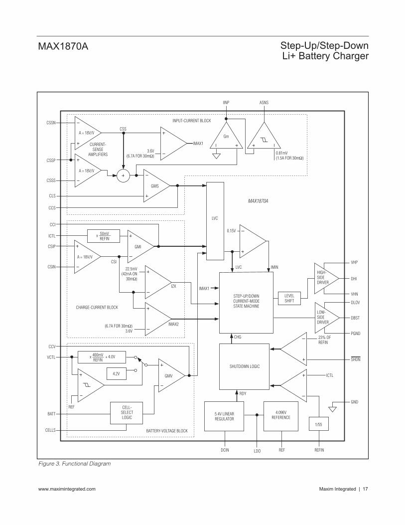
Detailed DescriptionThe MAX1870A includes all of the functions necessaryto charge Li+, NiMH, and NiCd batteries. A high-effi-ciency H-bridge topology DC-DC converter controlscharge voltage and current. A proprietary controlscheme offers improved efficiency and smaller inductorsize compared to conventional H-bridge controllers andoperates from input voltages above and below the bat-tery voltage. The MAX1870A includes analog controlinputs to limit the AC adapter current, charge current,and battery voltage. An analog output (IINP) delivers acurrent proportional to the source current. The TypicalApplication Circuit shown in Figure 1 uses a microcon-troller (µC) to control the charge current or voltage,while Figure 2 shows a typical application with thecharge voltage and current fixed to specific values forthe application. The voltage at ICTL and the value ofRS2 set the charge current. The voltage at VCTL andthe CELLS inputs set the battery regulation voltage forthe charger. The voltage at CLS and the value of R3 andR4 set the source current limit.The MAX1870A features a voltage-regulation loop(CCV) and two current-regulation loops (CCI and CCS).CCV is the compensation point for the battery voltageregulation loop. CCI and CCS are the compensationpoints for the battery charge current and supply currentloops, respectively. The MAX1870A regulates theadapter current by reducing battery charge currentaccording to system load demands.
Setting the Charge VoltageThe MAX1870A provides high-accuracy regulation ofthe charge voltage. Apply a voltage to VCTL to adjustthe battery-cell voltage limit. Set VCTL to a voltagebetween 0 and VREFIN for a 10% adjustment of the bat-tery cell voltage, or connect VCTL to LDO for a defaultsetting of 4.2V per cell. The limited adjustment rangereduces the sensitivity of the charge voltage to externalresistor tolerances. The overall accuracy of the chargevoltage is better than ±1% when using ±1% resistors todivide down the reference to establish VCTL. The per-cell battery-termination voltage is a function of the bat-tery chemistry and construction. Consult the batterymanufacturer to determine this voltage. Calculate bat-tery voltage using the following equation:
where NCELLS is the cell count selected by CELLS.VCTL is ratiometric with respect to REFIN to improveaccuracy when using resistive voltage-dividers.Connect CELLS as shown in Table 1 to charge two,three, or four cells. The cell count can either be hard-wired or software controlled. The internal error amplifier(GMV) maintains voltage regulation (see Figure 3 forthe Functional Diagram). Connect a 10kΩ resistor inseries with a 0.01µF capacitor from CCV to GND tocompensate the battery voltage loop. See the VoltageLoop Compensation section for more information.
Setting the Charge CurrentSet the maximum charge current using ICTL and thecurrent-sense resistor RS2 connected between CSIPand CSIN. The current threshold is set by the ratio ofVICTL / VREFIN. Use the following equation to programthe battery charge current:
where VCSIT is the full-scale charge current-sensethreshold, 73mV (typ). The input range for ICTL is VREFIN / 32 to VREFIN. To shut down the MAX1870A,force ICTL below VREFIN / 100.The internal error amplifier (GMI) maintains charge- current regulation (see Figure 3 for the FunctionalDiagram). Connect a 0.01µF capacitor from CCI to GNDto compensate the charge-current loop. See the Charge-Current Loop Compensation section for more information.
Setting the Input Current LimitThe total input current, from a wall adapter or other DCsource, is a function of the system supply current andthe battery charge current. The MAX1870A limits the walladapter current by reducing the charge current when theinput current exceeds the input current-limit set point. Asthe system supply current rises, the available chargecurrent decreases linearly to zero in proportion to thesystem current. After the charge current has fallen tozero, the MAX1870A cannot further limit the wall adaptercurrent if the system current continues to increase.
IVR
xVVCHG
CSIT
S
ICTL
REFIN=
2
V N x V V xVVBATT CELLS
VCTL
REFIN= +
⎛⎝⎜
⎞⎠⎟4 0 4.
CELLS CELL COUNT
GND 2
Float 3
REFIN 4
MAX1870A Step-Up/Step-Down Li+ Battery Charger
Maxim Integrated | 17www.maximintegrated.com
MAX1870A
CSSN
CSSP
CSSS
CLS
CCS
ICTL
CCI
CSIP
CSIN
CCV
BATT
CELLS
VCTL
A = 18V/V
A = 18V/V
CSS
CURRENT-SENSE
AMPLIFIERS3.6V
(6.7A FOR 30mΩ)
IMAX1
INPUT-CURRENT BLOCK
GMS
IINP ASNS
Gm
0.81mV(1.5A FOR 30mΩ)
50mVREFIN
x
400mVREFIN
x
GMI
A = 18V/VCSI
22.5mV(42mA ON
30mΩ)
(6.7A FOR 30mΩ)3.6V
IZX
IMAX2
CHARGE-CURRENT BLOCK
+ 4.0V
4.2V GMV
REF CELL-SELECTLOGIC
BATTERY-VOLTAGE BLOCK
SHUTDOWN LOGIC
5.4V LINEARREGULATOR
4.096VREFERENCE
DCIN LDO REF REFIN
1/55
CHG
RDY
ICTL
23% OFREFIN
GND
PGND
DLOV
VHN
DHI
VHP
DBST
SHDN
LEVELSHIFT
STEP-UP/DOWNCURRENT-MODESTATE MACHINE
IMAX1
LVC IMIN
0.15V
LVC
LOW-SIDEDRIVER
HIGH-SIDEDRIVER
Figure 3. Functional Diagram

MAX1870A Step-Up/Step-Down Li+ Battery Charger
Maxim Integrated | 18www.maximintegrated.com
The input source current is the sum of the MAX1870Aquiescent current, the charger input current, and thesystem load current. The MAX1870A’s 6mA maximumquiescent current is minimal compared to the chargeand load currents. The actual wall adapter current isdetermined as follows:
where η is the efficiency of the DC-DC converter (85%to 95% typ), ISYS_LOAD is the system load current,IADAPTER is the adapter current, and ICHARGE is thecharge current.By controlling the input current, the current require-ments of the AC wall adapter are reduced, minimizingsystem size and cost. Since charge current is reducedto control input current, priority is given to system loads.An internal amplifier compares the sum of (VCSSP -VCSSN) and (VCSSP - VCSSS) to a scaled voltage set bythe CLS input. Drive VCLS directly or set with a resistivevoltage-divider between REF and GND. Connect CLSto REF for the maximum input current limit of 105mV.Sense resistors RS1a and RS1b set the maximum-allowable wall adapter current. Use the same values forRS1a, RS1b, and RS2. Calculate the maximum walladapter current as follows:
where VCSST is the full-scale source current-sense volt-age threshold, and is 105mV (typ). The internal erroramplifier (GMS) maintains input-current regulation (seeFigure 3 for the Functional Diagram). Typically, connecta 0.01µF capacitor from CCS to GND to compensatethe source current loop (GMS). See the Charge-Currentand Wall-Adapter-Current Loop Compensation for moreinformation.
Input Current MeasurementThe MAX1870A includes an input-current monitor out-put, IINP. IINP is a scaled-down replica of the systemload current plus the input-referred charge current. Theoutput voltage range for IINP is 0 to 3.5V. The voltageof IINP is proportional to the output current by the fol-lowing equation:
VIINP = IADAPTER x RS1_ x GIINP x R7where IADAPTER is the DC current supplied by the AC adapter, GIINP is the transconductance of IINP(2.8µA/mV typ), and R7 is the resistor connectedbetween IINP and ground.
In the Typical Application Circuit, the duty cycle andAC load current affect the accuracy of VIINP (see theTypical Operating Characteristics).
LDO RegulatorLDO provides a 5.4V supply derived from DCIN. Thelow-side MOSFET driver is powered by DLOV, whichmust be connected to LDO as shown in Figure 1. LDOalso supplies the 4.096V reference (REF) and most ofthe internal control circuitry. Bypass LDO to GND with a1µF or greater ceramic capacitor. Bypass DLOV toPGND with a 1µF or greater ceramic capacitor.
AC Adapter DetectionThe MAX1870A includes a logic output, ASNS, whichindicates AC adapter presence. When the system loaddraws more than 1.5A (for 30mΩ sense resistors andR7 is 10kΩ), the ASNS logic output pulls high.
ShutdownWhen the AC adapter is removed, the MAX1870A shutsdown to a low-power state, and typically consumes lessthan 1µA from the battery through the combined load ofthe CSIP, CSIN, BLKP, and BATT inputs. The chargerenters this low-power state when DCIN falls below theundervoltage-lockout (UVLO) threshold of 7.5V.Alternatively, drive SHDN below 23.5% of VREFIN ordrive ICTL below VREFIN / 100 to inhibit charge. Thissuspends switching and pulls CCI, CCS, and CCV toground. The LDO, input current monitor, and controllogic all remain active in this state.
Step-Up/Step-Down
DC-DC ControllerThe MAX1870A is a step-up/step-down DC-DC con-troller. The MAX1870A controls a low-side n-channelMOSFET and a high-side p-channel MOSFET to a con-stant output voltage with input voltage variation above,near, and below the output. The MAX1870A implementsa control scheme that delivers higher efficiency withsmaller components and less output ripple when com-pared with other step-up/step-down control algorithms.This occurs because the MAX1870A operates withlower inductor currents, as shown in Figure 4.The MAX1870A proprietary algorithm offers the follow-ing benefits:• Inductor current requirements are minimized.• Low inductor-saturation current requirements allow
the use of physically smaller inductors.• Low inductor current improves efficiency by reducing
I2R losses in the MOSFETs, inductor, and senseresistors.
IVV
xVRSADAPTER MAX
CLS
REF
CSST_ _
=1
I II x V
V xADAPTER SYS LOADCHARGE BATT
IN= +_
η

MAX1870A Step-Up/Step-Down Li+ Battery Charger
Maxim Integrated | 19www.maximintegrated.com
• Continuous output current for VIN > 1.4 x VOUTreduces output ripple.
The MAX1870A uses the state machine shown in Figure5. The controller switches between the states A, B, and C,depending on VIN and VBATT. State D provides PFMoperation during light loads. Under moderate and heavyloads the MAX1870A operates in PWM.
Step-Down Operation (VIN > 1.4 x VBATT)During medium and heavy loads when VIN > 1.4 xVBATT, the MAX1870A alternates between state A andstate B, keeping MOSFET M2 off (Figure 5). Figure 6shows the inductor current in step-down operation.During this mode, the MAX1870A regulates the step-down off-time. Initially, DHI switches M1 off (state A) andthe inductor current ramps down with a dI/dt of VBATT / Luntil a target current is reached (determined by the errorintegrator). After the target current is reached, DHIswitches M1 on (state B), and the inductor current ramps
up with a dI/dt of (VIN - VBATT) / L. M1 remains on until astep-down on-time timer expires. This on-time is calculat-ed based on the input and output voltage to maintainpseudo-fixed-frequency 400kHz operation. At the end ofstate B, another step-down off-time (state A) is initiatedand the cycle repeats. The off-time is valley regulatedaccording to the error signal. The error signal is set bythe charge current or source current if either is at its limit,or the battery voltage if both charge current and sourcecurrent are below their respective current limits.During light loads, when the inductor current falls tozero during state A, the controller switches to state D toreduce power consumption and avoid shuttling currentin and out of the output.
Step-Up Operation (VIN < 0.9 x VBATT)When VIN < 0.9 x VBATT, the MAX1870A alternatesbetween state B and state C, keeping MOSFET M1 on.In this mode, the controller looks like a simple step-upcontroller. Figure 7 shows the inductor current in step-
A) CONVENTIONALALGORITHM
B) MAX1870AALGORITHM
2 x ICHARGE
SHADED REGIONS REPRESENT CHARGE DELIVERED
TIME
Figure 4. Inductor Current for VIN = VBATT
Table 2. MAX1870A H-Bridge Controller Advantages
MAX1870A H-BRIDGE CONTROLLER TRADITIONAL H-BRIDGE CONTROLLER
• Only 1 MOSFET switched per cycle• Continuous output current in step-down mode
• 2 MOSFETs switched per cycle• Always discontinuous output current
(requires higher inductor currents)

MAX1870A Step-Up/Step-Down Li+ Battery Charger
Maxim Integrated | 20www.maximintegrated.com Maxim Integrated | 20www.maximintegrated.com
up operation. During this mode, the MAX1870A regu-lates the step-up on-time. Initially DBST switches M2 on(state C) and the inductor current ramps up with a dI/dtof VIN / L. After the inductor current crosses the targetcurrent (set by the error integrators), DBST switches M2off (state B) and the inductor current ramps down witha dI/dt of (VBATT - VIN) / L. M2 remains off until a step-up off-time timer expires. This off-time is calculatedbased on the input and output voltage to maintain400kHz pseudo-fixed-frequency operation. The step-upon-time is regulated by the error signal, set accordingto the charge current or source current if either is at itslimit, or the battery voltage if both charge current andsource current are below their respective current limits.
Step-Up/Step-Down Operation (0.9 x VBATT < VIN < 1.4 x VBATT)The MAX1870A features a step-up/step-down modethat eliminates dropout. Figure 8 shows the inductorcurrent in step-up/step-down operation. When VIN iswithin 10% of VBATT, the MAX1870A alternates through
states A, B, and C, following the order A, B, C, B, A, B,C, etc., with the majority of the time spent in state B.Since more time is spent in state B, the inductor ripplecurrent is reduced, improving efficiency.The time in state C is peak-current regulated, and theremaining time is spent in state B (Figure 8A). Duringthis operating mode, the average inductor current isapproximately 20% higher than the load current.The time in state A is valley current and the remainingtime is spent in state B (Figure 8B). During this mode,the average inductor current is approximately 10%higher than the load current.Alternative algorithms require inductor currents twiceas high, resulting in four times larger I2R losses andinductors typically four times larger in volume.
IMIN, IMAX, CCMP, and ZCMPThe MAX1870A state machine utilizes five comparatorsto decide which state to be in and when to switchstates (Figure 3). The MAX1870A generates an error
VIN VOUT
M1 D3
D4 M2
STEP-DOWN OFF
VIN VOUT
M1
M2
STEP-DOWN ON
STATE BSTATE A STATE C
VIN VOUT
M1
M2
STEP-DOWN PFM
IDLE STATE D
VIN VOUT
M1
M2
+ -STEP-DOWNPWM
STEP-UPPWM
STEP-UP OFF STEP-UP ON
D4
D2
D4
D3
D3
D3
Figure 5. MAX1870A State Machine

MAX1870A Step-Up/Step-Down Li+ Battery Charger
Maxim Integrated | 21www.maximintegrated.com Maxim Integrated | 21www.maximintegrated.com
STATE B
STATE A
PRECALCULATED STEP-DOWN ON-TIME
VALLEY REGULATED OFF-TIME
dldt
VIN - VOUTL=
dldt
VOUTL=
VIN > 1.4 x VBATT DUTY = VIN / VOUT
Figure 6. MAX1870A Step-Down Inductor Current Waveform
signal based on the integrated error of the input cur-rent, charge current, and battery voltage. The error sig-nal, determined by the lowest voltage clamp (LVC),sets the threshold for current-mode regulation. The fol-lowing comparators are used for regulation:• IMIN: The MAX1870A operates in discontinuous
conduction if LVC is below 0.15V, and does not ini-tiate another step-down on-time. In discontinuousstep-up conduction, the peak current is set by
IMIN. The peak inductor current in discontinuousstep-up mode is:
where VIMIN is the IMIN comparator threshold,0.15V, and ACSI is the charge current-sense ampli-fier gain, 18V/V.
IV
A x RSPKIMIN
CSI>
2
STATE B
STATE C
PRECALCULATED OFF-TIME
PEAK REGULATED ON-TIMEdldt
VIN - VOUTL=
dldt
VOUTL=
VIN > 0.9 x VBATT DUTY = 1 - VIN / VOUT
Figure 7. Step-Up Inductor-Current Waveform

MAX1870A Step-Up/Step-Down Li+ Battery Charger
Maxim Integrated | 22www.maximintegrated.com
• CCMP: CCMP compares the current-mode controlpoint, LVC, to the inductor current. In step-downmode, the off-time (state A) is terminated when theinductor current falls below the current thresholdset by LVC. In step-up mode, the on-time (state C)is terminated when the inductor current rises abovethe current threshold set by LVC.
• IMAX: The IMAX comparators provide a cycle-by-cycle inductor current limit. This circuit comparesthe inductor current (CSI in step-down mode orCSS in step-up mode) to the internally fixed cycle-
by-cycle current limit. The current-sense voltagelimit is 200mV. With RS1_ = RS2 = 30mΩ, whichcorresponds to 6.7A. If the inductor current-sensevoltage is greater than VIMAX (200mV), a step-upon-time is terminated or a step-down on-time is notpermitted.
• ZCMP: The ZCMP comparator detects when theinductor current crosses zero. If the ZCMP outputgoes high during a step-down off-t ime, theMAX1870A switches to the idle state (state D) toconserve power.
STATE C
STATE B
STATE A
STATE B
STATE A
STATE B
STATE C STATE B
A)
B)
MINIMUMSTEP-DOWN
OFF-TIME
PRECALCULATED STEP-UPOFF-TIME
PRECALCULATED STEP-DOWNON-TIME
PRECALCULATED STEP-DOWNON-TIME
MINIMUMSTEP-UPON-TIME
PEAK REGULATEDSTEP-UPON-TIME
VALLEY REGULATEDSTEP-DOWN
OFF-TIME
dldt
VBATT - VINL=
dldt
VINL= dl
dtVBATT
L=
Figure 8. MAX1870A Step-Up/Step-Down Inductor-Current Waveform

MAX1870A Step-Up/Step-Down Li+ Battery Charger
Maxim Integrated | 23www.maximintegrated.com
Switching FrequencyThe MAX1870A includes input and output-voltage feed-forward to maintain pseudo-fixed-frequency (400kHz)operation. The time in state B is set according to theinput voltage, output voltage, and a time constant. Instep-up/step-down mode the switching frequency iseffectively cut in half to allow for both the step-up cycleand the step-down cycle. The switching frequency istypically between 350kHz and 405kHz for VIN between8V and 28V. See the Typical Operating Characteristics.
CompensationEach of the three regulation loops (the battery voltage,the charge current, and the input current limit) are com-pensated separately using the CCV, CCI, and CCSpins, respectively. Compensate the voltage regulationloop with a 10kΩ resistor in series with a 0.01µF capaci-tor from CCV to GND. Compensate the charge currentloop and source current loop with 0.01µF capacitorsfrom CCI to GND and from CCS to GND, respectively.
Voltage Loop CompensationWhen regulating the charge voltage, the MAX1870Abehaves as a current-mode step-down or step-uppower supply. Since a current-mode controller regulatesits output current as a function of the error signal, theduty-cycle modulator can be modeled as a GM stage(Figure 9). Results are similar in step-down, step-up, orstep-up/down, with the exception of a load-dependentright-half-plane zero that occurs in step-up mode.The required compensation network is a pole-zero pairformed with CCV and RCV. CCV is chosen to be largeenough that its impedance is relatively small comparedto RCV at frequencies near crossover. RCV sets thegain of the error amplifier near crossover. RCV andCOUT determine the crossover frequency and, there-fore, the closed-loop response of the system and theresponse time upon battery removal.RESR is the equivalent series resistance (ESR) of thecharger’s output capacitor (COUT). RL is the equivalentcharger output load, RL = ΔVBATT / ΔICHG = RBATT.The equivalent output impedance of the GMV amplifier,ROGMV, is greater than 10MΩ. The voltage looptransconductance (GMV = ΔICCV / ΔVBATT) scalesinversely with the number of cells. GMV = 0.1µA/mV forfour cells, 0.133µA/mV for three cells, and 0.2µA/mV fortwo cells. The DC-DC converter’s transconductancedepends upon the charge current-sense resistor RS2:
where ACSI = 18, and RS2 = 30mΩ in the TypicalApplication Circuits, so GMPWM = 1.85A/V.
Use the following equation to calculate the loop transferfunction (LTF):
The poles and zeros of the voltage-loop transfer func-tion are listed from lowest frequency to highest frequen-cy in Table 3.Near crossover, CCV has much lower impedance thanROGMV. Since CCV is in parallel with ROGMV, CCV dom-inates the parallel impedance near crossover.Additionally, RCV has a much higher impedance thanCCV and dominates the series combination of RCV andCCV, so:
COUT also has a much lower impedance than RL nearcrossover, so the parallel impedance is mostly capaci-tive and:
If RESR is small enough, its associated output zero hasa negligible effect near crossover and the loop transferfunction can be simplified as follows:
RsC x R sC
L
OUT L OUT( )11
+≅
R x sC x RsC x R
R near crossoverOGMV CV CV
CV OGMVCV
( )( )
,1
1+
+≅
LTF GM xR x sC R
sC x Rx
RsC x R
x G x sC x R
PWMOGMV CV CV
CV OGMV
L
OUT LMV OUT ESR
=+
+
++
( )( )
( )( )
11
11
GMA x RSPWM
CSI=
12
GMOUT
REF
GMV
RLRESR
COUT
RORCV
CCV
BATT
CCV
Figure 9. CCV Simplified Loop Diagram

MAX1870A Step-Up/Step-Down Li+ Battery Charger
Maxim Integrated | 24www.maximintegrated.com
Setting the LTF = 1 to solve for the unity-gain frequencyyields:
For stability, choose a crossover frequency lower than1/10th of the switching frequency. The crossover fre-quency must also be below the RHP zero, calculated atmaximum charge current, minimum input voltage, andmaximum battery voltage.Choosing a crossover frequency of 13kHz and solving forRCV using the component values listed in Figure 1 yields:MODE = VCC (4 cells) GMV = 0.1µA/mVCOUT = 22µF GMPWM = 1.85A/VVBATT= 16.8V fCO_CV = 13kHz
RL = 0.2Ω fOSC = 400kHz
To ensure that the compensation zero adequately can-cels the output pole, select fZ_CV ≤ fP_OUT.
CCV ≥ (RL / RCV) x COUTCCV ≥ 440pF
Figure 10 shows the Bode Plot of the voltage-loop fre-quency response using the values calculated above.
Charge-Current and Wall-Adapter-CurrentLoop CompensationWhen the MAX1870A regulates the charge current or thewall adapter current, the system stability does notdepend on the output capacitance. The simplifiedschematic in Figure 11 describes the operation of theMAX1870A when the charge-current loop (CCI) is in con-trol. The simplified schematic in Figure 12 describes theoperation of the MAX1870A when the source-current
Rx C x f
GMV x GMkCV
OUT CO CV
PWM= =
210
π _ Ω
f GM x GRx CCO CV PWM MV
CV
OUT_ =
⎛
⎝⎜
⎞
⎠⎟2π
LTF GM xR
sCGPWM
CV
OUTMV=
Table 3. Constant Voltage Loop Poles and Zeros
NO. NAME CALCULATION DESCRIPTION
1 CCV PoleLowest Frequency Pole created by CCV and GMV’s finite outputresistance. Since ROGMV is very large (ROGMV > 10MΩ), this isa low-frequency pole.
2 CCV Zero
Voltage-Loop Compensation Zero. If this zero is lower than theoutput pole, fP_OUT, then the loop transfer functionapproximates a single-pole response near the crossoverfrequency. Choose CCV to place this zero at least 1 decadebelow crossover to ensure adequate phase margin.
3Output
Pole
Outp ut P ol e For m ed w i th the E ffecti ve Load Resi stance RL and theOutp ut C ap aci tance C OU T . RL i nfl uences the D C g ai n b ut d oes notaffect the stab i l i ty of the system or the cr ossover fr eq uency.
4OutputZero
Output ESR Zero. This zero can keep the loop from crossingunity gain if fZ_OUT is less than the desired crossoverfrequency. Therefore, choose a capacitor with an ESR zerogreater than the crossover frequency.
5 RHP Zero
S tep - U p M od e RH P Z er o. Thi s zer o occur s b ecause of the i ni ti al op p osi ng r esp onse of a step - up conver ter . E ffor ts to i ncr ease thei nd uctor cur r ent r esul t i n an i m m ed i ate d ecr ease i n cur r entd el i ver ed , al thoug h eventual l y r esul t i n an i ncr ease i n cur r entd el i ver ed . Thi s zer o i s d ep end ent on char g e cur r ent and m aycause the system to g o unstab l e at hi g h cur r ents w hen i n step - up m od e. A r i g ht- hal f- p l ane zer o i s d etr i m ental to b oth p hase and g ai n. To ensur e stab i l i ty und er m axi m um l oad i n step - up m od e,the cr ossover fr eq uency m ust b e l ow er than hal f of fR H P Z .
fx R CP CV
OGMV CV_ =
12π
fx R CZ CV
CV CV_ =
12π
fx R CP OUT
L OUT_ =
12π
fx R CZ OUT
ESR OUT_ =
12π
fVx L I
Vx L I V
RHPZIN
L
IN
OUT OUT
=
=
2
2
2
π
π

MAX1870A Step-Up/Step-Down Li+ Battery Charger
Maxim Integrated | 25www.maximintegrated.com
loop (CCS) is in control. Since the output capacitor’simpedance has little effect on the response of the currentloop, only a single pole is required to compensate thisloop. ACSI and ACSS are the internal gains of the current-sense amplifiers. RS2 is the charge current-sense resis-tor. RS1a and RS1b are the adapter current-senseresistors. ROGMI and ROGMS are the equivalent outputimpedance of the GMI and GMS amplifiers, which aregreater than 10MΩ. GMI is the charge-current amplifiertransconductance (2.4µA/mV). GMS is the adapter-cur-rent amplifier transconductance (1.7µA/mV.) GMPWM isthe DC-DC converter transconductance (1.85A/V).Use the following equation to calculate the loop transferfunction:
which describes a single-pole system. Since GMPWM =
the loop-transfer function simplifies to:
Use the following equations to calculate the crossoverfrequency:
For stability, choose a crossover frequency lower than1/10th of the switching frequency and lower than half ofthe RHP zero.CCI = 10 GMI / (2π x fOSC), CCS = 10 GMS / (2π x fOSC)
This zero is inversely proportional to charge currentand may cause the system to go unstable at high cur-rents when in step-up mode. A right-half-plane zero isdetrimental to both phase and gain. To also ensure sta-bility under maximum load in step-up mode, the CCIcrossover frequency must also be lower than fRHPZ.The right-half-plane zero does not affect CCS.Choosing a crossover frequency of 30kHz and usingthe component values listed in Figure 1 yields CCI andCCS_ > 10nF. Values for CCI / CCS greater than tentimes the minimum value may slow down the currentloop response excessively. Figure 13 shows the BodePlot of the input-current frequency response using thevalues calculated above.
MOSFET DriversDHI and DBST are optimized for driving moderately-sized power MOSFETs. Use low-inductance and low-resistance traces from driver outputs to MOSFET gates.DHI typically sources 1.6A and sinks 0.8A to or fromthe gate of the p-channel MOSFET. DHI swings fromVHP to VHN. VHN is a negative LDO that regulates withrespect to VHP to provide high-side gate drive.Connect VHP to DCIN. Bypass VHN with a 1µF capaci-tor to VHP.
fV
x L IV
L I VRHPZ WorstCaseIN MIN
L
IN MIN
OUTMAX OUTMAX_
_ _= =2 2
2
π π
fGMI
Cf
GMSCCO CI
CICO CS
CS_ _,= =
2 2π π
LTF GMR
sR x COGM
OGM C=
+_ _
_ _1
1A x RSCS_ _
LTF GM x A x RS x GMR
sR x CPWM CSOGM
OGM C=
+_ _ _ _
_ _1
CCV LOOP RESPONSE
MAG
NITU
DE (d
B)
-135
-90
-45
080
60
40
20
-40
-20
0
1.E+00 1.E+01 1.E+02 1.E+03 1.E+04 1.E+05 1.E+061.E-01
FREQUENCY (Hz)
MAG
PHASE
Figure 10. CCV Loop Response
GMPWM
REF
GMI
ROGMI
CCI
CCI
RS2
ACSI
CSI
Figure 11. CCI Simplified Loop Diagram

MAX1870A Step-Up/Step-Down Li+ Battery Charger
Maxim Integrated | 26www.maximintegrated.com
LDO provides a 5.4V supply derived from DCIN anddelivers over 10mA. The n-channel MOSFET driverDBST is powered by DLOV and can source 2.5A andsink 5A. Since LDO provides power to the internal ana-log circuitry, use an RC filter from LDO to DLOV asshown in Figure 1 to minimize noise at LDO. LDO alsosupplies the 4.096V reference (REF) and most of theinternal control circuitry. Bypass LDO with a 1µF orgreater capacitor to GND.
Applications Information
Component SelectionTable 4 lists the recommended components and refersto the circuit of Figure 1. The following sections describehow to select these components.
MOSFETsThe MAX1870A requires one p-channel MOSFET andone n-channel MOSFET. Component substitutions arepermissible as long as the on-resistance and gatecharge are equal or lower and the voltage, current, andpower-dissipation ratings are high enough. If using alower-power application, scale down the MOSFETs withlower gate charge and the MOSFET’s on-resistancecan be scaled up. For example, in a system designedto deliver half as much current, MOSFETs selected withtwice the on-resistance and half as much gate chargeensure equal or better efficiency, and reduce size andcost. If resistive losses dominate, it can be possible toreduce the gate charge at the cost of on-resistanceand still achieve a similar efficiency.Make sure that the linear regulators can drive theselected MOSFETs. The average current required todrive a given MOSFET is:
ILDO = QgM2 x fswitchIVHN = QgM1 x fswitch
where fswitch is 400kHz (typ).
GMPWM
ROGMSCCS
CCS
CLSCSS
GMS
ACSS
CSSP
CSSN/CSSS
RS1_
Figure 12. CCS Simplified Loop Diagram
CCI LOOP RESPONSE
MAG
NITU
DE (d
B)
-90
-45
0
80
60
40
20
-40
-20
0
100
1k100.1 100k
FREQUENCY (Hz)
CCS LOOP RESPONSE
MAG
NITU
DE (d
B)
-90
-45
0
80
60
40
20
-40
-20
0
100
1k100.1 100k 10M
FREQUENCY (Hz)
PHASE PHASE
MAG
MAG
Figure 13. CCI and CCS Loop Response

MAX1870A Step-Up/Step-Down Li+ Battery Charger
Maxim Integrated | 27www.maximintegrated.com
MOSFET Power DissipationTable 5 shows the resistive losses and switching lossesin each of the MOSFETs during either step-up or step-down operation. Table 5 provides a first-order estimate,but does not consider second-order effects such asripple current or nonlinear gate drive.For typical applications where VBATT / 2 < VIN < 2 xVBATT, the resistive losses are primarily dissipated in M1since M2 operates at a lower duty cycle. Switching loss-es are dissipated in M1 when in step-down mode and inM2 when in step-up mode. Ratio the MOSFETs so thatresistive losses roughly equal switching losses when atmaximum load and typical input/output conditions. Theresistive loss equations are a good approximation inhybrid mode (VIN near VBATT). Both M1 and M2 switch-ing losses apply in hybrid mode.Switching losses can become a heat problem when themaximum AC adapter voltage is applied in step-downoperation or minimum AC adapter voltage is appliedwith a maximum battery voltage. This behavior occursbecause of the squared term in the CV2 f switching-lossequation. Table 5 provides only an estimate and is nota substitute for breadboard evaluation.
Inductor SelectionSelect the inductor to minimize power dissipation in theMOSFETs, inductor, and sense resistors. To optimizeresistive losses and RMS inductor current, set the LIR(inductor current ripple) to 0.3. Because the maximumresistive power loss occurs at the step-up boundary of
hybrid mode, select LIR for operating in this mode. Selectthe inductance according to the following equation:
Larger inductance values can be used; however, theycontribute extra resistance that can reduce efficiency.Smaller inductance values increase RMS currents andcan also reduce efficiency.
Saturation Current RatingThe inductor must have a saturation current rating highenough so it does not saturate at full charge, maximumoutput voltage, and minimum input voltage. In step-upoperation, the inductor carries a higher current than instep-down operation with the same load. Calculate theinductor saturation current rating by the followingequation:
Input-Capacitor SelectionThe input capacitor must meet the ripple currentrequirement (IRMS) imposed by the switching currents.Nontantalum chemistries (ceramic, aluminum, or OS-
IV x I
V
T x V xV
Vx L
SATOUT MAX CHG MAX
IN MIN
IN MININ MIN
OUT MAX
≥ +
−⎛⎝⎜
⎞⎠⎟
_ _
_
__
_1
2
Lx V x tLIR I
IN
CHG=
2 min
Table 4. Component List
DESIGNATION PART SPECIFICATIONS
INDUCTORS
L1
Sumida CDRH104R-100Sumida CDRH104R-7R0Sumida CDRH104R-5R2Sumida CDRH104R-3R8
10µH, 4.4A, 35mΩ power inductor7µH, 4.8A, 27mΩ power inductor5.2µH, 5.5A, 22mΩ power inductor3.8µH, 6A, 13mΩ power inductor
P-CHANNEL MOSFETs
M1
Siliconix Si4435DYFairchild FDC602PFairchild FDS4435AFairchild FDW256P
P-FET 35mΩ, QG = 17nC, VDSMAX = 30V, 8-pin SOP-FET 35mΩ, QG = 14nC, VDSMAX = 20V, 6-pin SuperSOTP-FET 25mΩ, QG = 21nC, VDSMAX = 30V, 8-pin SOP-FET 20mΩ, QG = 28nC, VDSMAX = 30V, 8-pin TSSOP
N/P-CHANNEL MOSFET PAIRS
M1/M2 Fairchild FDW2520C (8-pin TSSOP)N-FET 18mΩ, QG = 14nC, VDSMAX = 20V,P-FET 35mΩ, QG = 14nC, VDSMAX = 20V
N-CHANNEL MOSFETs
M2 IRF7811W N-FET, 9mΩ, QG = 18nC, VDSMAX = 30V, 8-pin SO

MAX1870A Step-Up/Step-Down Li+ Battery Charger
Maxim Integrated | 28www.maximintegrated.com
CON) are preferred due to their resilience to power-upsurge currents.The input capacitors should be sized so that the temper-ature rise due to ripple current in continuous conductiondoes not exceed approximately 10°C. Choose a capaci-tor with a ripple current rating higher than 0.5 x ICHG.
Output-Capacitor SelectionThe output capacitor absorbs the inductor ripple currentin step-down mode, or a peak-to-peak ripple currentequal to the inductor current when in step-up or hybridmode. As such, both capacitance and ESR are impor-tant parameters in specifying the output capacitor. Theactual amplitude of the ripple is the combination of thetwo. Ceramic devices are preferable because of theirresilience to surge currents. The worst-case output rippleoccurs during hybrid mode when the input voltage is atits minimum. See the Typical Operating Characteristics.Select a capacitor that can handle 0.5 x ICHG x VBATT /VIN while keeping the rise in capacitor temperature lessthan 10°C. Also, select the output capacitor to toleratethe surge current delivered from the battery when it isinitially plugged into the charger.
Battery-Removal ResponseUpon battery removal, the MAX1870A continues to reg-ulate a constant inductor current until the battery volt-age, VBATT, exceeds the regulation threshold. TheMAX1870A’s response time depends on the bandwidthof the CCV loop, fCO (see the Voltage LoopCompensation section). For applications where batteryovershoot is critical, either increase COUT or increasefCO by increasing RCV. See Battery Insertion andRemoval in the Typical Operating Characteristics.
System Load TransientThe MAX1870A battery charger features a very fastresponse time to system load transients. Since theinput current loop is configured as a single-pole sys-tem, the MAX1870A responds quickly to system loadtransients (see the System Load-Transient Responsegraph in the Typical Operating Characteristics). Thisreduces the risk of tripping the overcurrent threshold ofthe wall adapter and minimizes requirements foradapter oversizing.
Table 5. MOSFET Resistive and Switching LossesSTEP-DOWN MODE STEP-UP MODE
DESIGNATIONDC LOSSES
M1
D4 0
M2 0
D3 ICHG x VDIODE ICHG x VDIODE
SWITCHING LOSSES
M1 0
D4 0 0
M2 0
D3 0 0
Note: CLX is the total parasitic capacitance at the drain terminals of M1 and M2. IGATE is the peak gate-drive source/sink current ofM1 or M2.
VV
x I x RBATT
DCINCHG DS ON
⎛⎝⎜
⎞⎠⎟ 2 ( )
VV
x I x RBATT
DCINCHG DS ON
⎛⎝⎜
⎞⎠⎟
2( )
1 −⎛⎝⎜
⎞⎠⎟
VV
x I VBATT
DCINCHG Diode
12
−⎛⎝⎜
⎞⎠⎟
⎛⎝⎜
⎞⎠⎟
VV
xVV
x I x RDCIN
BATT
BATT
DCINCHG DS ON( )
V x C x f II
DCIN MAX LX SW CHG
GATE
( )2
V x C x f II x V
BATT MAX LX SW CHG
GATE DCIN MAX
( )
( )
3

MAX1870A Step-Up/Step-Down Li+ Battery Charger
Maxim Integrated | 29www.maximintegrated.com
Layout and BypassingBypass DCIN with a 1µF to ground (Figure 1). Optionaldiodes D1 and D2 protect the MAX1870A when the DCpower-source input is reversed. A signal diode for D1 isadequate because DCIN only powers the LDO and theinternal reference. Good PC board layout is required toachieve specified noise, efficiency, and stable perfor-mance. The PC board layout artist must be givenexplicit instructions—preferably, a pencil sketch show-ing the placement of the power-switching componentsand high-current routing. Refer to the PC board layoutin the MAX1870A evaluation kit for examples. A groundplane is essential for optimum performance. In mostapplications, the circuit is located on a multilayerboard, and full use of the four or more copper layers isrecommended. Use the top layer for high-current con-nections (PGND, DHI, VHP, VHN, BLKP, and DLOV),the bottom layer for quiet connections (CSSP, CSSN,CSSS, CSIP, CSIN, REF, CCV, CCI, CCS, DCIN, LDOand GND), and the inner layers for an uninterruptedground plane. Use the following step-by-step guide:1) Place the high-power connections first, with their
grounds adjacent:• Minimize the current-sense resistor trace lengths,
and ensure accurate current sensing with Kelvinconnections. Use independent branches for CSSP,CSSS, CSSN, CSIP, and CSIN.
• Minimize ground trace lengths in the high-currentpaths.
• Minimize other trace lengths in the high-current paths.• Use >5mm wide traces for high-current paths.
Ideally, surface-mount power components are flushagainst one another with their ground terminals almosttouching. These high-current grounds are then connect-ed to each other with a wide, filled zone of top-layer cop-per, so they do not go through vias. Other high-currentpaths should also be minimized, but focus primarily onshort ground and current-sense connections to eliminateabout 90% of all PC board layout problems.2) Place the IC and signal components. Keep the main
switching nodes (inductor connections) away fromsensitive analog components (current-sense tracesand REF capacitor). Important: the IC must be nofurther than 10mm from the current-sense resis-tors. Keep the gate-drive traces (DHI and DBST)shorter than 20mm, and route them away from thecurrent-sense lines and REF. Place ceramic bypasscapacitors close to the IC. The bulk capacitors canbe placed further away. Bypass CSSP, CSSN, CSIN,and CSIP to analog GND to reduce switching noiseand maintain input-current and charger-current accu-racy. Place the current-sense input filter capacitorsunder the part, connected directly to GND.
3) Use a single-point star ground placed directlybelow the part. Connect the input ground trace,power ground (subground plane), and normalground to this node.
Figure 14 shows a partial layout of the power path andcomponents. Refer to the EV kit data sheet for moreinformation.

MAX1870A Step-Up/Step-Down Li+ Battery Charger
Maxim Integrated | 30www.maximintegrated.com
MAX1870A
THIN QFN
TOP VIEW
32
31
30
29
28
27
26
9
10
11
12
13
14
15
18192021222324
7654321
REF
LDO
CLS
GND
CCV
CCI
CCS
8GN
D
DCIN
CSSP
CSSS
CSSN
VHP
DHI
VHN
25DLOV
I.C.
PGND
DBST
I.C.
I.C.
BLKP
CSIP
17CS
IN
SHDN
IINP
16 BATT
CELLS
ICTL
VCTL
ASNS
REFIN
Pin Configuration
N P M1
M2
D3 D4
RS1a
RS1b
C8
C9
RS2
IN
BATT
PGND
LOAD
L1
Figure 14. Recommended Layout for the MAX1870A
Chip InformationTRANSISTOR COUNT: 6484PROCESS: BiCMOS
PACKAGETYPE
PACKAGECODE
OUTLINE NO.LAND
PATTERN NO.
32 TQFN T3255+4 21-0140 90-0012
Package InformationFor the - package outline information and land patterns (foot-prints), go to www.maximintegrated.com/packages. Note that a“+”, “#”, or “-” in the package code indicates RoHS status only.Package drawings may show a different suffix character, but thedrawing pertains to the package regardless of RoHS status.

MAX1870A Step-Up/Step-Down Li+ Battery Charger
Maxim Integrated cannot assume responsibility for use of any circuitry other than circuitry entirely embodied in a Maxim Integrated product. No circuit patentlicenses are implied. Maxim Integrated reserves the right to change the circuitry and specifications without notice at any time. The parametric values (min andmax limits) shown in the Electrical Characteristics table are guaranteed. Other parametric values quoted in this data sheet are provided for guidance.
Maxim Integrated and the Maxim Integrated logo are trademarks of Maxim Integrated Products, Inc. © 2015 Maxim Integrated Products, Inc. | 31
For pricing, delivery, and ordering information, please contact Maxim Direct at 1-888-629-4642, or visit Maxim Integrated’s website at www.maximintegrated.com.
Revision History
REVISION NUMBER
REVISION DATE
DESCRIPTION PAGES CHANGED
2 5/15 Updated Benefits and Features section 1
3 8/15 Updated Figures 1 and 2 14, 15
Top Related