


Languages
Pages
Legal

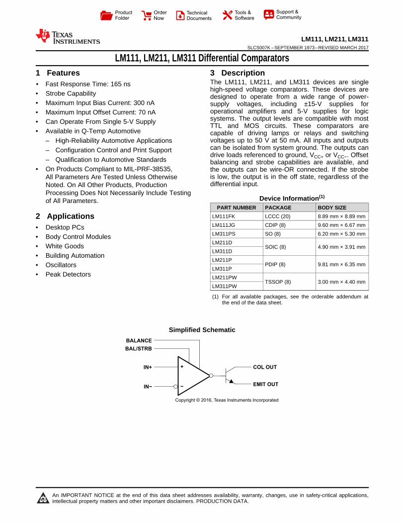
BAL/STRB
COL OUT
IN−
IN+
BALANCE
EMIT OUT
+
−
Copyright © 2016, Texas Instruments Incorporated
Product
Folder
Order
Now
Technical
Documents
Tools &
Software
Support &Community
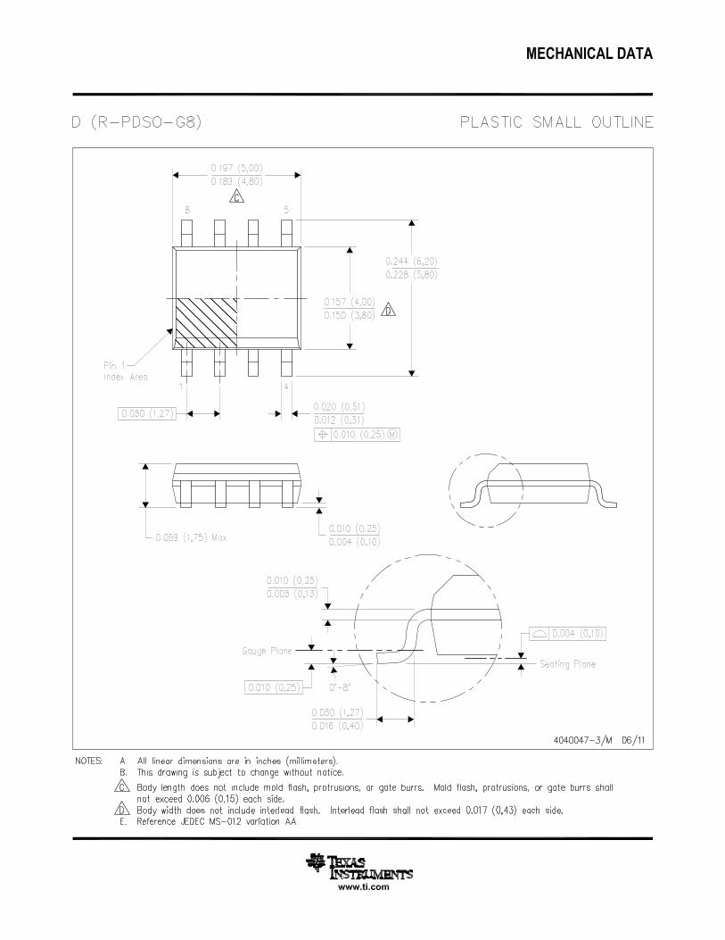
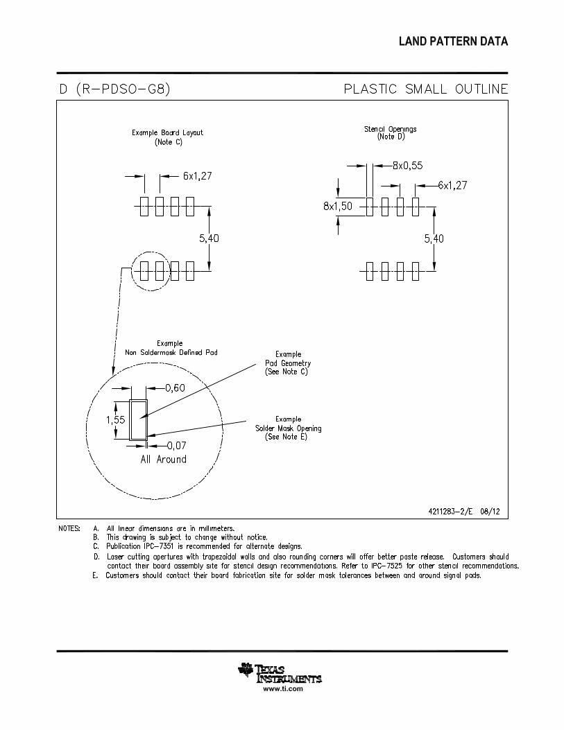
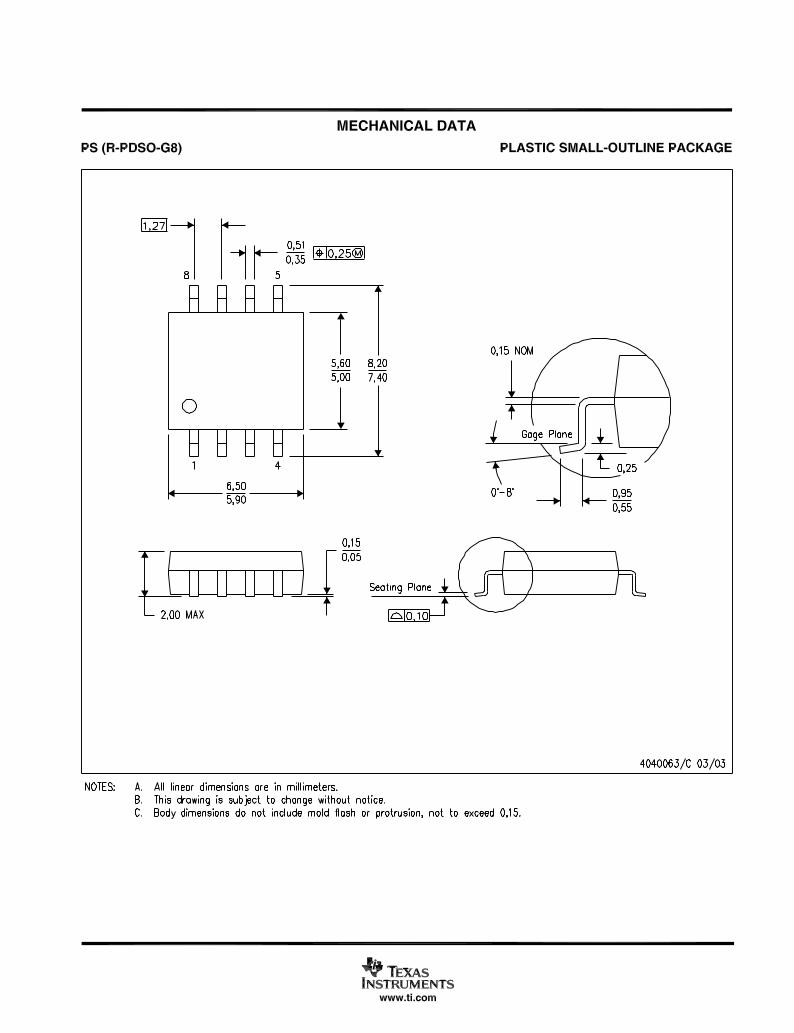
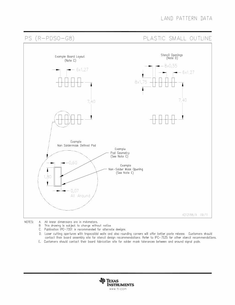
An IMPORTANT NOTICE at the end of this data sheet addresses availability, warranty, changes, use in safety-critical applications,intellectual property matters and other important disclaimers. PRODUCTION DATA.
LM111, LM211, LM311SLCS007K –SEPTEMBER 1973–REVISED MARCH 2017
LM111, LM211, LM311 Differential Comparators
1
1 Features1• Fast Response Time: 165 ns• Strobe Capability• Maximum Input Bias Current: 300 nA• Maximum Input Offset Current: 70 nA• Can Operate From Single 5-V Supply• Available in Q-Temp Automotive
– High-Reliability Automotive Applications– Configuration Control and Print Support– Qualification to Automotive Standards
• On Products Compliant to MIL-PRF-38535,All Parameters Are Tested Unless OtherwiseNoted. On All Other Products, ProductionProcessing Does Not Necessarily Include Testingof All Parameters.
2 Applications• Desktop PCs• Body Control Modules• White Goods• Building Automation• Oscillators• Peak Detectors
3 DescriptionThe LM111, LM211, and LM311 devices are singlehigh-speed voltage comparators. These devices aredesigned to operate from a wide range of power-supply voltages, including ±15-V supplies foroperational amplifiers and 5-V supplies for logicsystems. The output levels are compatible with mostTTL and MOS circuits. These comparators arecapable of driving lamps or relays and switchingvoltages up to 50 V at 50 mA. All inputs and outputscan be isolated from system ground. The outputs candrive loads referenced to ground, VCC+ or VCC−. Offsetbalancing and strobe capabilities are available, andthe outputs can be wire-OR connected. If the strobeis low, the output is in the off state, regardless of thedifferential input.
Device Information(1)
PART NUMBER PACKAGE BODY SIZELM111FK LCCC (20) 8.89 mm × 8.89 mmLM111JG CDIP (8) 9.60 mm × 6.67 mmLM311PS SO (8) 6.20 mm × 5.30 mmLM211D
SOIC (8) 4.90 mm × 3.91 mmLM311DLM211P
PDIP (8) 9.81 mm × 6.35 mmLM311PLM211PW
TSSOP (8) 3.00 mm × 4.40 mmLM311PW
(1) For all available packages, see the orderable addendum atthe end of the data sheet.
SPACER
Simplified Schematic
2
LM111, LM211, LM311SLCS007K –SEPTEMBER 1973–REVISED MARCH 2017 www.ti.com
Product Folder Links: LM111 LM211 LM311
Submit Documentation Feedback Copyright © 1973–2017, Texas Instruments Incorporated
Table of Contents1 Features .................................................................. 12 Applications ........................................................... 13 Description ............................................................. 14 Revision History..................................................... 25 Pin Configuration and Functions ......................... 36 Specifications......................................................... 4
6.1 Absolute Maximum Ratings ..................................... 46.2 ESD Ratings.............................................................. 46.3 Recommended Operating Conditions....................... 46.4 Thermal Information (8-Pin Packages) ..................... 56.5 Thermal Information (20-Pin Package) ..................... 56.6 Electrical Characteristics........................................... 66.7 Switching Characteristics .......................................... 66.8 Typical Characteristics .............................................. 7
7 Parameter Measurement Information .................. 98 Detailed Description ............................................ 10
8.1 Overview ................................................................. 108.2 Functional Block Diagram ....................................... 10
8.3 Feature Description................................................. 118.4 Device Functional Modes........................................ 11
9 Application and Implementation ........................ 129.1 Application Information............................................ 129.2 Typical Application ................................................. 129.3 System Examples ................................................... 14
10 Power Supply Recommendations ..................... 2211 Layout................................................................... 22
11.1 Layout Guidelines ................................................. 2211.2 Layout Example .................................................... 22
12 Device and Documentation Support ................. 2312.1 Related Links ........................................................ 2312.2 Receiving Notification of Documentation Updates 2312.3 Community Resources.......................................... 2312.4 Trademarks ........................................................... 2312.5 Electrostatic Discharge Caution............................ 2312.6 Glossary ................................................................ 23
13 Mechanical, Packaging, and OrderableInformation ........................................................... 23
4 Revision HistoryNOTE: Page numbers for previous revisions may differ from page numbers in the current version.
Changes from Revision J (January 2017) to Revision K Page
• Changed Human body model (HBM) from: ±1000 to: ±500 in ESD Ratings table ................................................................ 4
Changes from Revision I (June 2015) to Revision J Page
• Changed the data sheet title From: LMx11 Quad Differential Comparators To: LM111, LM211, LM311 DifferentialComparators .......................................................................................................................................................................... 1
• Updated the Applications list ................................................................................................................................................. 1• Updated the Thermal Information (8-Pin Packages) table ..................................................................................................... 5• Changed text From: "over a −25°C to +85°C temperature range..." To: ""over a −40°C to +85°C temperature
range..." in the Overview section.......................................................................................................................................... 10• Added text "The LM311 has a temperature range of −40°C to +125°C." to the Overview section...................................... 10
Changes from Revision H (August 2003) to Revision I Page
• Updated Features with Military Disclaimer. ............................................................................................................................ 1• Added Applications, Device Information table, Pin Configuration and Functions section, ESD Ratings table, Feature
Description section, Device Functional Modes, Application and Implementation section, Power SupplyRecommendations section, Layout section, Device and Documentation Support section, and Mechanical,Packaging, and Orderable Information section. No specification changes. ........................................................................... 1
3 2 1 20 19
9 10 11 12 13
4
5
6
7
8
18
17
16
15
14
NC
COL OUT
NC
BAL/STRB
NC
NC
IN+
NC
IN−
NC
NC
EM
ITO
UT
NC
BA
LA
NC
E
NC
NC
NC
NC
CC
−V
CC
+V
1
2
3
4
8
7
6
5
EMIT OUT
IN+
IN−
VCC−
VCC+
COL OUT
BAL/STRB
BALANCE
3
LM111, LM211, LM311www.ti.com SLCS007K –SEPTEMBER 1973–REVISED MARCH 2017
Product Folder Links: LM111 LM211 LM311
Submit Documentation FeedbackCopyright © 1973–2017, Texas Instruments Incorporated
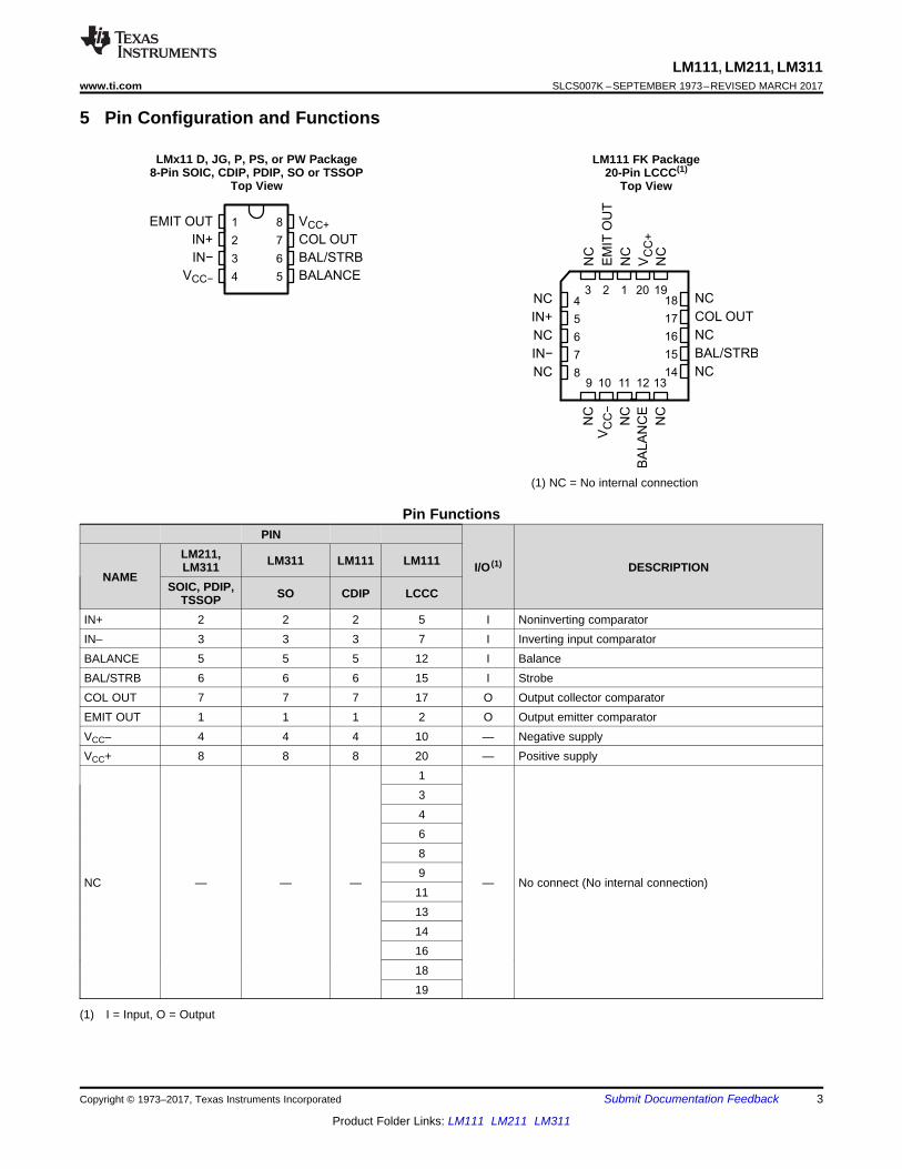
5 Pin Configuration and Functions
LMx11 D, JG, P, PS, or PW Package8-Pin SOIC, CDIP, PDIP, SO or TSSOP
Top View
LM111 FK Package20-Pin LCCC(1)
Top View
(1) NC = No internal connection
(1) I = Input, O = Output
Pin FunctionsPIN
I/O (1) DESCRIPTIONNAME
LM211,LM311 LM311 LM111 LM111
SOIC, PDIP,TSSOP SO CDIP LCCC
IN+ 2 2 2 5 I Noninverting comparatorIN– 3 3 3 7 I Inverting input comparatorBALANCE 5 5 5 12 I BalanceBAL/STRB 6 6 6 15 I StrobeCOL OUT 7 7 7 17 O Output collector comparatorEMIT OUT 1 1 1 2 O Output emitter comparatorVCC– 4 4 4 10 — Negative supplyVCC+ 8 8 8 20 — Positive supply
NC — — —
1
— No connect (No internal connection)
34689
111314161819
4
LM111, LM211, LM311SLCS007K –SEPTEMBER 1973–REVISED MARCH 2017 www.ti.com
Product Folder Links: LM111 LM211 LM311
Submit Documentation Feedback Copyright © 1973–2017, Texas Instruments Incorporated
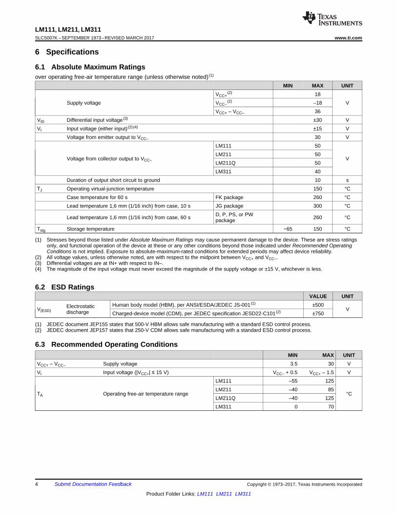
(1) Stresses beyond those listed under Absolute Maximum Ratings may cause permanent damage to the device. These are stress ratingsonly, and functional operation of the device at these or any other conditions beyond those indicated under Recommended OperatingConditions is not implied. Exposure to absolute-maximum-rated conditions for extended periods may affect device reliability.
(2) All voltage values, unless otherwise noted, are with respect to the midpoint between VCC+ and VCC–.(3) Differential voltages are at IN+ with respect to IN–.(4) The magnitude of the input voltage must never exceed the magnitude of the supply voltage or ±15 V, whichever is less.
6 Specifications
6.1 Absolute Maximum Ratingsover operating free-air temperature range (unless otherwise noted) (1)
MIN MAX UNIT
Supply voltageVCC+
(2) 18VVCC–
(2) –18VCC+ – VCC– 36
VID Differential input voltage (3) ±30 VVI Input voltage (either input) (2) (4) ±15 V
Voltage from emitter output to VCC– 30 V
Voltage from collector output to VCC–
LM111 50
VLM211 50LM211Q 50LM311 40
Duration of output short circuit to ground 10 sTJ Operating virtual-junction temperature 150 °C
Case temperature for 60 s FK package 260 °CLead temperature 1,6 mm (1/16 inch) from case, 10 s JG package 300 °C
Lead temperature 1,6 mm (1/16 inch) from case, 60 s D, P, PS, or PWpackage 260 °C
Tstg Storage temperature −65 150 °C
(1) JEDEC document JEP155 states that 500-V HBM allows safe manufacturing with a standard ESD control process.(2) JEDEC document JEP157 states that 250-V CDM allows safe manufacturing with a standard ESD control process.
6.2 ESD RatingsVALUE UNIT
V(ESD)Electrostaticdischarge
Human body model (HBM), per ANSI/ESDA/JEDEC JS-001 (1) ±500V
Charged-device model (CDM), per JEDEC specification JESD22-C101 (2) ±750
6.3 Recommended Operating ConditionsMIN MAX UNIT
VCC+ – VCC– Supply voltage 3.5 30 VVI Input voltage (|VCC+| ≤ 15 V) VCC– + 0.5 VCC+ – 1.5 V
TA Operating free-air temperature range
LM111 –55 125
°CLM211 –40 85LM211Q –40 125LM311 0 70
5
LM111, LM211, LM311www.ti.com SLCS007K –SEPTEMBER 1973–REVISED MARCH 2017
Product Folder Links: LM111 LM211 LM311
Submit Documentation FeedbackCopyright © 1973–2017, Texas Instruments Incorporated
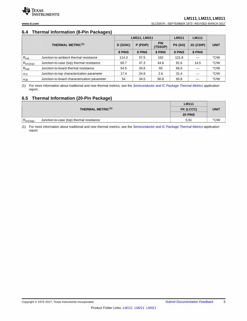
(1) For more information about traditional and new thermal metrics, see the Semiconductor and IC Package Thermal Metrics applicationreport.
6.4 Thermal Information (8-Pin Packages)
THERMAL METRIC (1)
LM211, LM311 LM311 LM111
UNITD (SOIC) P (PDIP) PW(TSSOP) PS (SO) JG (CDIP)
8 PINS 8 PINS 8 PINS 8 PINS 8 PINSRθJA Junction-to-ambient thermal resistance 114.3 57.5 162 121.8 — °C/WRθJC(top) Junction-to-case (top) thermal resistance 60.7 47.3 44.6 81.6 14.5 °C/WRθJB Junction-to-board thermal resistance 54.5 34.6 93 66.5 — °C/WψJT Junction-to-top characterization parameter 17.4 24.9 2.6 31.4 — °C/WψJB Junction-to-board characterization parameter 54 34.5 90.8 65.8 — °C/W
(1) For more information about traditional and new thermal metrics, see the Semiconductor and IC Package Thermal Metrics applicationreport.
6.5 Thermal Information (20-Pin Package)
THERMAL METRIC (1)LM111
UNITFK (LCCC)20 PINS
RθJC(top) Junction-to-case (top) thermal resistance 5.61 °C/W
6
LM111, LM211, LM311SLCS007K –SEPTEMBER 1973–REVISED MARCH 2017 www.ti.com
Product Folder Links: LM111 LM211 LM311
Submit Documentation Feedback Copyright © 1973–2017, Texas Instruments Incorporated
(1) Unless otherwise noted, all characteristics are measured with BALANCE and BAL/STRB open and EMIT OUT grounded. Full range forLM111 is –55°C to 125°C, for LM211 is –40°C to 85°C, for LM211Q is –40°C to 125°C, and for LM311 is 0°C to 70°C.
(2) All typical values are at TA = 25°C.(3) The offset voltages and offset currents given are the maximum values required to drive the collector output up to 14 V or down to 1 V
with a pullup resistor of 7.5 kΩ to VCC+. These parameters actually define an error band and take into account the worst-case effects ofvoltage gain and input impedance.
(4) The strobe must not be shorted to ground; it must be current driven at –3 mA to –5 mA (see Figure 18 and Figure 31).
6.6 Electrical Characteristicsat specified free-air temperature, VCC± = ±15 V (unless otherwise noted)
PARAMETER TEST CONDITIONS TA(1)
LM111LM211
LM211QLM311
UNIT
MIN TYP (2) MAX MIN TYP (2) MAX
VIO Input offset voltage See (3) 25°C 0.7 3 2 7.5mV
Full range 4 10
IIO Input offset current See (3) 25°C 4 10 6 50nA
Full range 20 70
IIB Input bias current 1 V ≤ VO ≤ 14 V25°C 75 100 100 250
nAFull range 150 300
IIL(S)Low-levelstrobe current (4)
V(strobe) = 0.3 V,VID ≤ –10 mV 25°C –3 –3 mA
VICR
Common-modeinput-voltagerange (3)
Lower rangeFull range
–14.7 –14.5 –14.7 –14.5V
Upper range 13 13.8 13 13.8
AVD
Large-signaldifferential-voltageamplification
5 V ≤ VO ≤ 35 V, RL = 1 kΩ 25°C 40 200 40 200 V/mV
IOH
High-level(collector)output leakagecurrent
I(strobe) = –3 mA,VID = 5 mV VOH = 35 V
25°C 0.2 10 nA
Full range 0.5 μA
VID = 5 mV, VOH = 35 V 25°C 0.2 50 nA
VOL
Low-level(collector-to-emitter)output voltage
IOL = 50 mAVID = –5 mV 25°C 0.75 1.5
VVID = –10 mV 25°C 0.75 1.5
VCC+ = 4.5 V,VCC– = 0 V,IOL = 8 mA
VID = –6 mV Full range 0.23 0.4
VID = –10 mV Full range 0.23 0.4
ICC+Supply current fromVCC+output low
VID = –10 mV, No load 25°C 5.1 6 5.1 7.5 mA
ICC–Supply current fromVCC–output high
VID = 10 mV, No load 25°C –4.1 –5 –4.1 –5 mA
(1) The response time specified is for a 100-mV input step with 5-mV overdrive and is the interval between the input step function and theinstant when the output crosses 1.4 V.
(2) The package thermal impedance is calculated in accordance with MIL-STD-883.
6.7 Switching CharacteristicsVCC± = ±15 V, TA = 25°C
PARAMETER TEST CONDITIONS
LM111LM211
LM211QLM311
UNIT
TYPResponse time, low-to-high-level outputSee (1)
RC = 500 Ω to 5 V, CL = 5 pF, see (2) 115 nsResponse time, high-to-low-level outputSee (1) 165 ns
7
LM111, LM211, LM311www.ti.com SLCS007K –SEPTEMBER 1973–REVISED MARCH 2017
Product Folder Links: LM111 LM211 LM311
Submit Documentation FeedbackCopyright © 1973–2017, Texas Instruments Incorporated
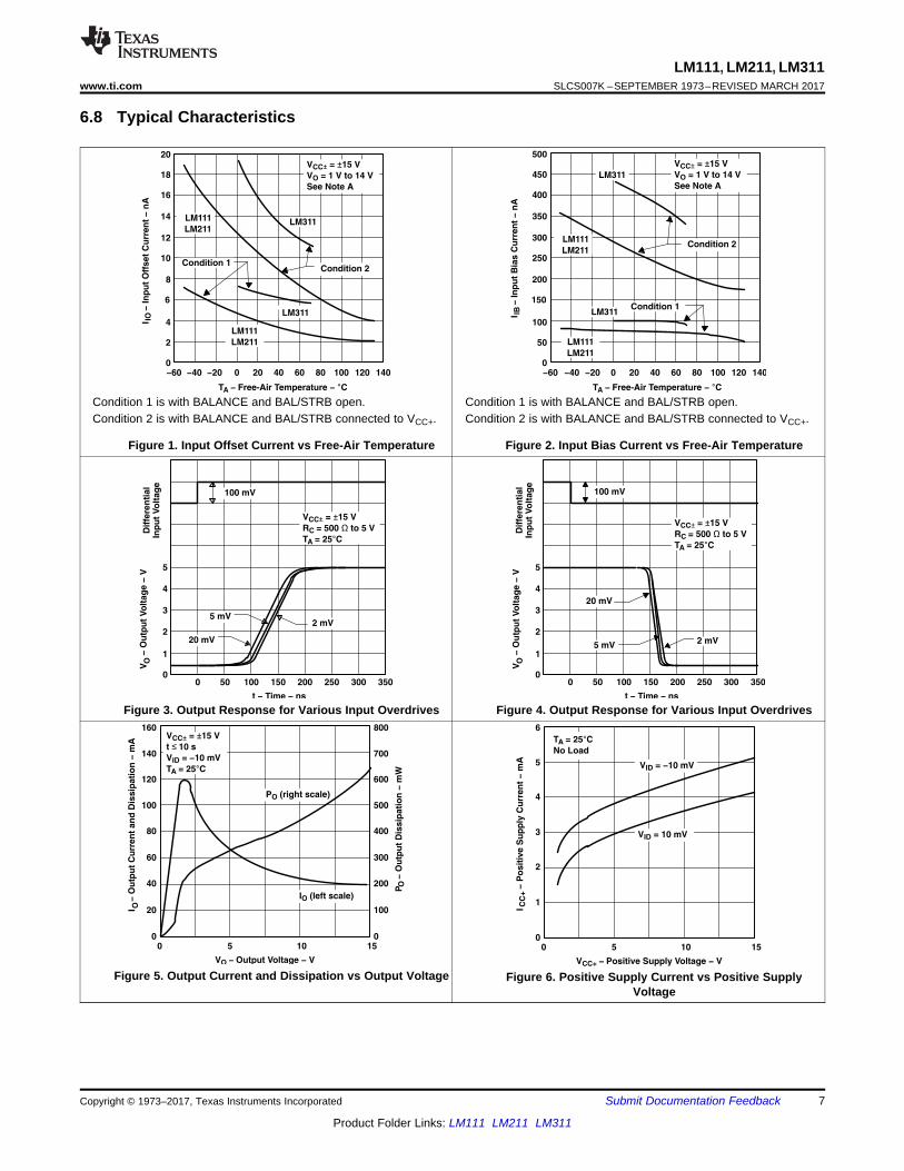
6.8 Typical Characteristics
Condition 1 is with BALANCE and BAL/STRB open.Condition 2 is with BALANCE and BAL/STRB connected to VCC+.
Figure 1. Input Offset Current vs Free-Air Temperature
Condition 1 is with BALANCE and BAL/STRB open.Condition 2 is with BALANCE and BAL/STRB connected to VCC+.
Figure 2. Input Bias Current vs Free-Air Temperature
Figure 3. Output Response for Various Input Overdrives Figure 4. Output Response for Various Input Overdrives
Figure 5. Output Current and Dissipation vs Output Voltage Figure 6. Positive Supply Current vs Positive SupplyVoltage
30
20
10
0−1 −0.5 0
−O
utp
ut
Vo
ltag
e−
V 40
50
60
0.5 1
VO
VID − Differential Input Voltage − mV
Collector
Output
RL = 1 kΩ
LM111
LM211
LM311
Emitter Output
RL = 600 Ω
VCC+ = 30 V
VCC− = 0
TA = 25°C
8
LM111, LM211, LM311SLCS007K –SEPTEMBER 1973–REVISED MARCH 2017 www.ti.com
Product Folder Links: LM111 LM211 LM311
Submit Documentation Feedback Copyright © 1973–2017, Texas Instruments Incorporated
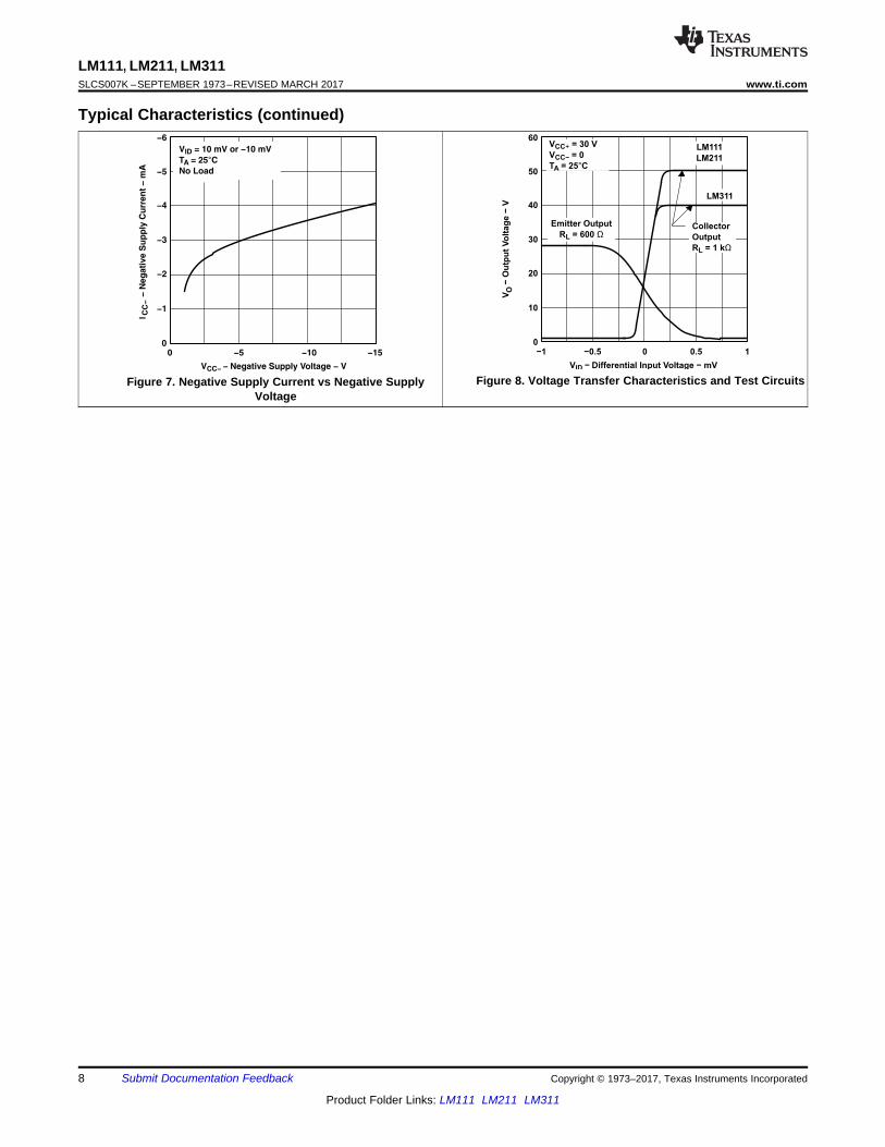
Typical Characteristics (continued)
Figure 7. Negative Supply Current vs Negative SupplyVoltage
Figure 8. Voltage Transfer Characteristics and Test Circuits
VID
VCC+ = 15 V
RE = 2 kΩ
VO
VCC− = −15 V
Copyright © 2016, Texas Instruments Incorporated
VID
VCC+ = 15 V
500 Ω
VO
VCC− = −15 V
5 V
Copyright © 2016, Texas Instruments Incorporated
VID
VCC+ = 30 V
1 kΩ
Output
VCC−
VI = 50 V (LM111, LM211)
40 V (LM311)
Copyright © 2016, Texas Instruments Incorporated
VID
VCC+ = 30 V
600 Ω
VCC−
Output
Copyright © 2016, Texas Instruments Incorporated
9
LM111, LM211, LM311www.ti.com SLCS007K –SEPTEMBER 1973–REVISED MARCH 2017
Product Folder Links: LM111 LM211 LM311
Submit Documentation FeedbackCopyright © 1973–2017, Texas Instruments Incorporated
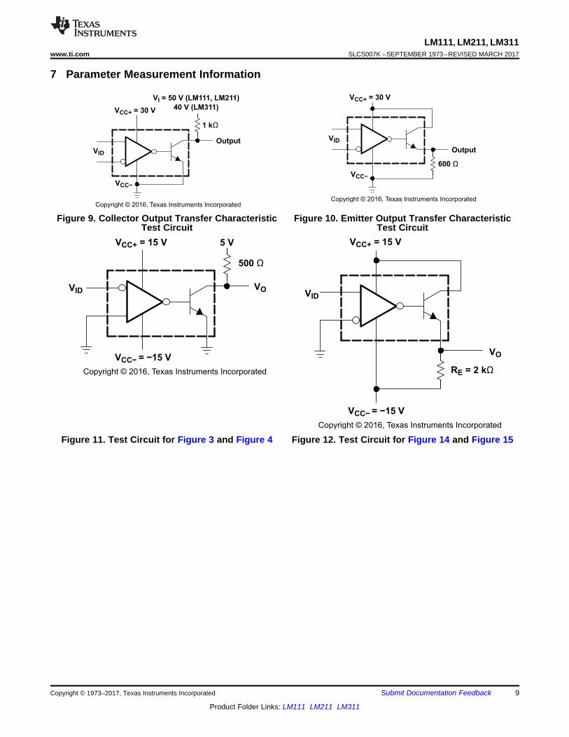
7 Parameter Measurement Information
Figure 9. Collector Output Transfer CharacteristicTest Circuit
Figure 10. Emitter Output Transfer CharacteristicTest Circuit
Figure 11. Test Circuit for Figure 3 and Figure 4 Figure 12. Test Circuit for Figure 14 and Figure 15
BAL/STRB BALANCE
IN+
IN−
450 Ω 450 Ω
2.4
kΩ
1.2 kΩ
70 Ω
2.4
kΩ
1.2 kΩ
60 Ω
400 Ω
450 Ω
2 kΩ
200 Ω250 Ω
600 Ω
130 Ω
4 Ω
4 kΩ
VCC+
VCC−
EMIT OUT
COL OUT
750 Ω 600 Ω
Component Count
Resistors 20
Diodes 2
EPI FET 1
Transistors 22
Copyright © 2016, Texas Instruments Incorporated
10
LM111, LM211, LM311SLCS007K –SEPTEMBER 1973–REVISED MARCH 2017 www.ti.com
Product Folder Links: LM111 LM211 LM311
Submit Documentation Feedback Copyright © 1973–2017, Texas Instruments Incorporated
8 Detailed Description
8.1 OverviewThe LM111, LM211 and LM311 are voltage comparators that have input currents nearly a thousand times lowerthan legacy standard devices. They are also designed to operate over a wider range of supply voltages: fromstandard ±15V op amp supplies down to the single 5-V supply used for IC logic. Their output is compatible withRTL, DTL and TTL as well as MOS circuits. Further, they can drive lamps or relays, switching voltages up to 50V at currents as high as 50 mA.
Both the inputs and the outputs of the LM111, LM211 or the LM311 can be isolated from system ground, and theoutput can drive loads referred to ground, the positive supply or the negative supply. Offset balancing and strobecapability are provided and outputs can be wire ORed. The LM211 is identical to the LM111, except that itsperformance is specified over a −40°C to +85°C temperature range instead of −55°C to +125°C. The LM311 hasa temperature range of 0°C to +70°C. The LM211Q has a temperature range of −40°C to +125°C.
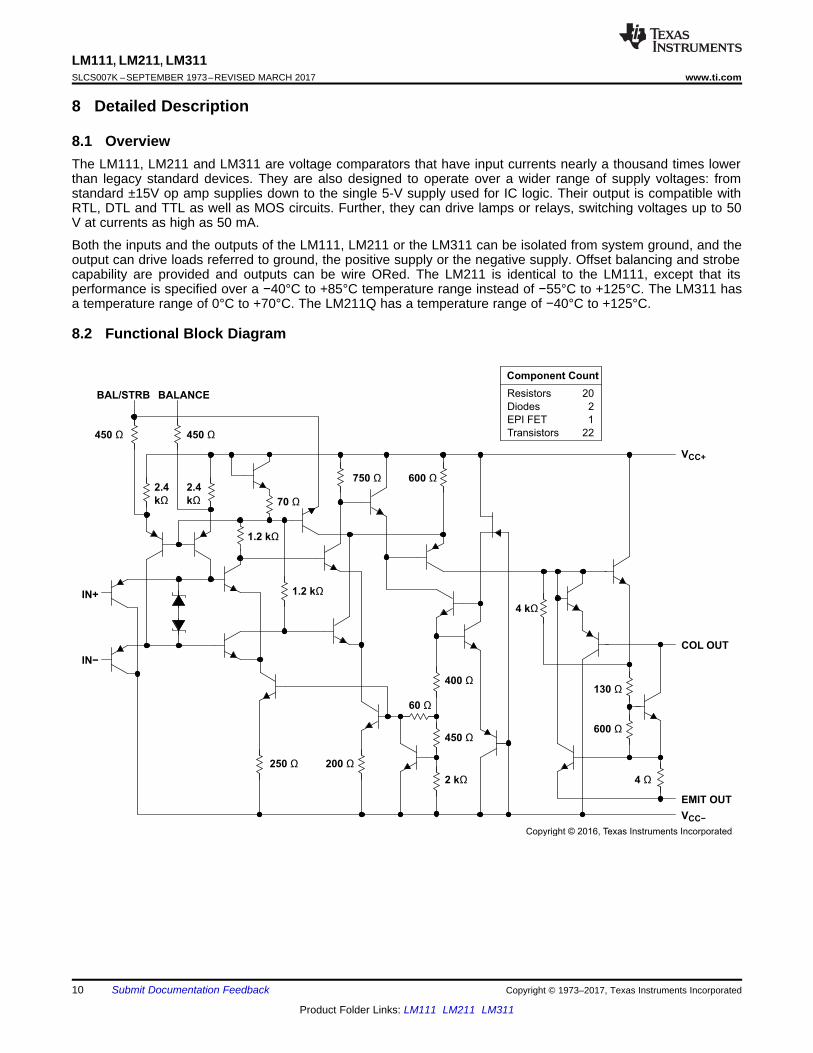
8.2 Functional Block Diagram
11
LM111, LM211, LM311www.ti.com SLCS007K –SEPTEMBER 1973–REVISED MARCH 2017
Product Folder Links: LM111 LM211 LM311
Submit Documentation FeedbackCopyright © 1973–2017, Texas Instruments Incorporated
8.3 Feature DescriptionLMx11 consists of a PNP input stage to sense voltages near VCC–. It also contains balance and strobe pins forexternal offset adjustment or trimming.
The input stage is followed by a very high gain stage for very fast response after a voltage difference on the inputpins have been sensed.
This is then followed by the output stage that consists of an open collector NPN (pulldown or low-side) transistor.Unlike most open drain comparators, this NPN output stage has an isolated emitter from VCC–, allowing thisdevice to set the VOL output value for collector output.
8.4 Device Functional Modes
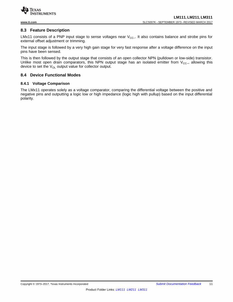
8.4.1 Voltage ComparisonThe LMx11 operates solely as a voltage comparator, comparing the differential voltage between the positive andnegative pins and outputting a logic low or high impedance (logic high with pullup) based on the input differentialpolarity.
VCC+
Input
VCC−
20 kΩ
Output
Copyright © 2016, Texas Instruments Incorporated
12
LM111, LM211, LM311SLCS007K –SEPTEMBER 1973–REVISED MARCH 2017 www.ti.com
Product Folder Links: LM111 LM211 LM311
Submit Documentation Feedback Copyright © 1973–2017, Texas Instruments Incorporated
9 Application and Implementation
NOTEInformation in the following applications sections is not part of the TI componentspecification, and TI does not warrant its accuracy or completeness. TI’s customers areresponsible for determining suitability of components for their purposes. Validate and testthe design implementation to confirm system functionality.
9.1 Application InformationA typical LMx11 application compares a single signal to a reference or two signals against each other. Manyusers take advantage of the open-drain output to drive the comparison logic output to a logic voltage level to anMCU or logic device. The wide supply range and high voltage capability makes LMx11 optimal for level shifting toa higher or lower voltage.
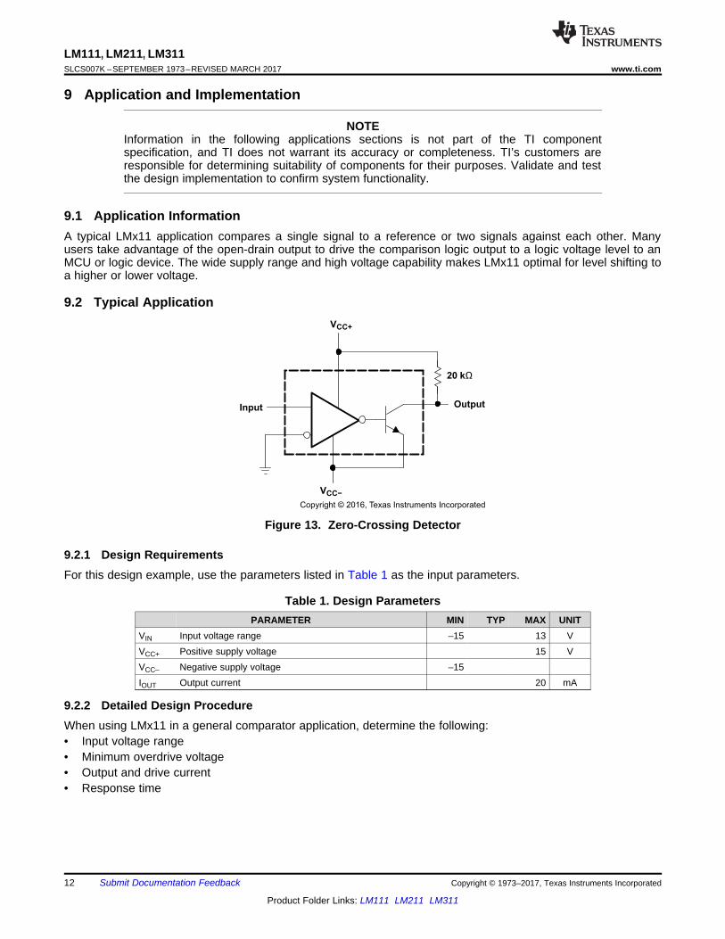
9.2 Typical Application
Figure 13. Zero-Crossing Detector
9.2.1 Design RequirementsFor this design example, use the parameters listed in Table 1 as the input parameters.
Table 1. Design ParametersPARAMETER MIN TYP MAX UNIT
VIN Input voltage range –15 13 VVCC+ Positive supply voltage 15 VVCC– Negative supply voltage –15IOUT Output current 20 mA
9.2.2 Detailed Design ProcedureWhen using LMx11 in a general comparator application, determine the following:• Input voltage range• Minimum overdrive voltage• Output and drive current• Response time
OLCE
OUT
VR
I=
N CE LR Ct @ ´
P PULLUP LR Ct @ ´
13
LM111, LM211, LM311www.ti.com SLCS007K –SEPTEMBER 1973–REVISED MARCH 2017
Product Folder Links: LM111 LM211 LM311
Submit Documentation FeedbackCopyright © 1973–2017, Texas Instruments Incorporated
9.2.2.1 Input Voltage RangeWhen choosing the input voltage range, consider the input common mode voltage range (VICR). Operationoutside of this range can yield incorrect comparisons.
The following list describes the outcomes of some input voltage situations.
• When both IN– and IN+ are both within the common-mode range:– If IN– is higher than IN+ and the offset voltage, the output is low and the output transistor is sinking
current– If IN– is lower than IN+ and the offset voltage, the output is high impedance and the output transistor is
not conducting• When IN– is higher than common mode and IN+ is within common mode, the output is low and the output
transistor is sinking current• When IN+ is higher than common mode and IN– is within common mode, the output is high impedance and
the output transistor is not conducting• When IN– and IN+ are both higher than common mode, the output is undefined
9.2.2.2 Minimum Overdrive VoltageOverdrive voltage is the differential voltage produced between the positive and negative inputs of the comparatorover the offset voltage (VIO). To make an accurate comparison the Overdrive voltage (VOD) must be higher thanthe input offset voltage (VIO). Overdrive voltage can also determine the response time of the comparator, with theresponse time decreasing with increasing overdrive. Figure 14 and Figure 15 show positive and negativeresponse times with respect to overdrive voltage.
9.2.2.3 Output and Drive CurrentOutput current is determined by the pullup resistance and pullup voltage. The output current produces a outputlow voltage (VOL) from the comparator, in which VOL is proportional to the output current. Use Figure 5 todetermine VOL based on the output current.
The output current can also effect the transient response.
9.2.2.4 Response TimeThe load capacitance (CL), pullup resistance (RPULLUP), and equivalent collector-emitter resistance (RCE) levelsdetermine the transient response. Equation 1 approximates the positive response time. Equation 2 approximatesthe negative response time. RCE can be determine by taking the slope of Figure 5 in the linear region at thedesired temperature, or by Equation 3.
(1)
(2)
where• VOL is the low-level output voltage• IOUT is the output current (3)
VCC+
39 kΩ
1200 pF
20 kΩ 1 kΩ
10 kΩ
20 kΩ
Square Wave
Output
(fanout to two
Series 54 gates,
or equivalent)
Copyright © 2016, Texas Instruments Incorporated
µ µ
14
LM111, LM211, LM311SLCS007K –SEPTEMBER 1973–REVISED MARCH 2017 www.ti.com
Product Folder Links: LM111 LM211 LM311
Submit Documentation Feedback Copyright © 1973–2017, Texas Instruments Incorporated
9.2.3 Application Curves
Figure 14. Output Response for Various Input Overdrives Figure 15. Output Response for Various Input Overdrives
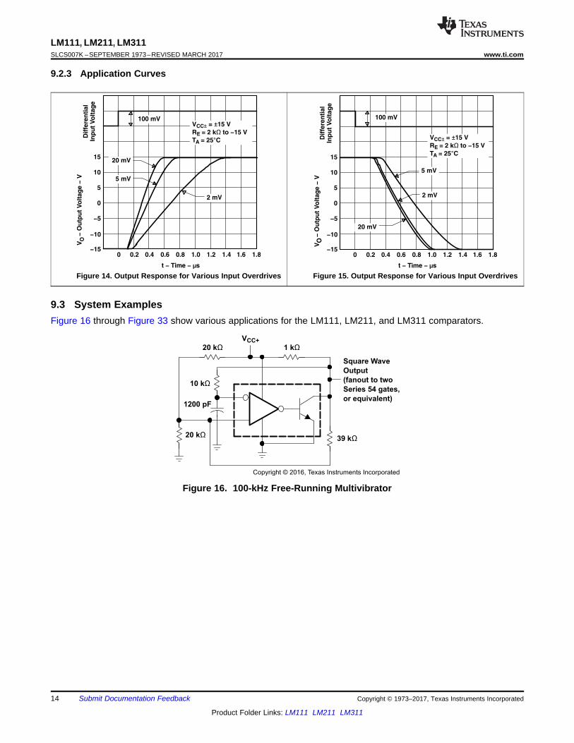
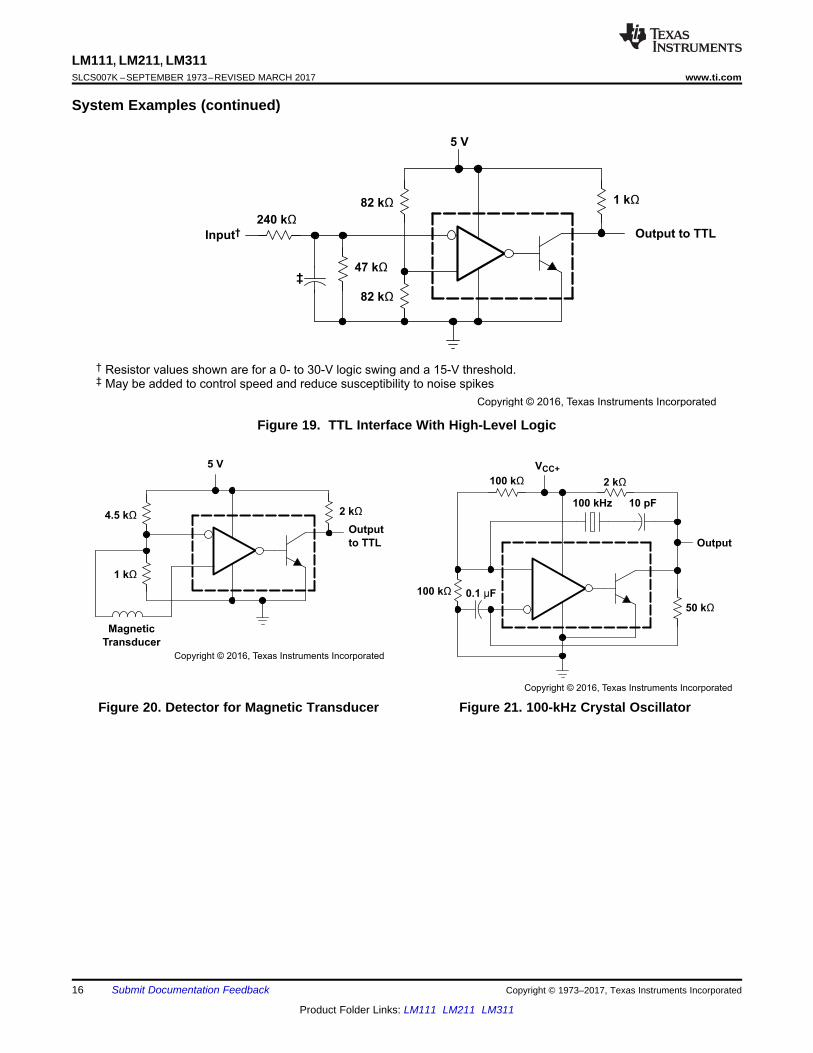
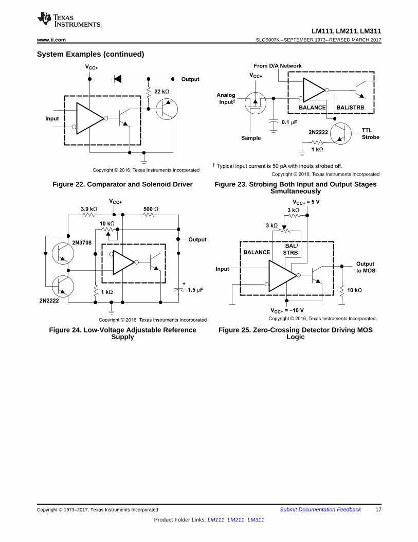
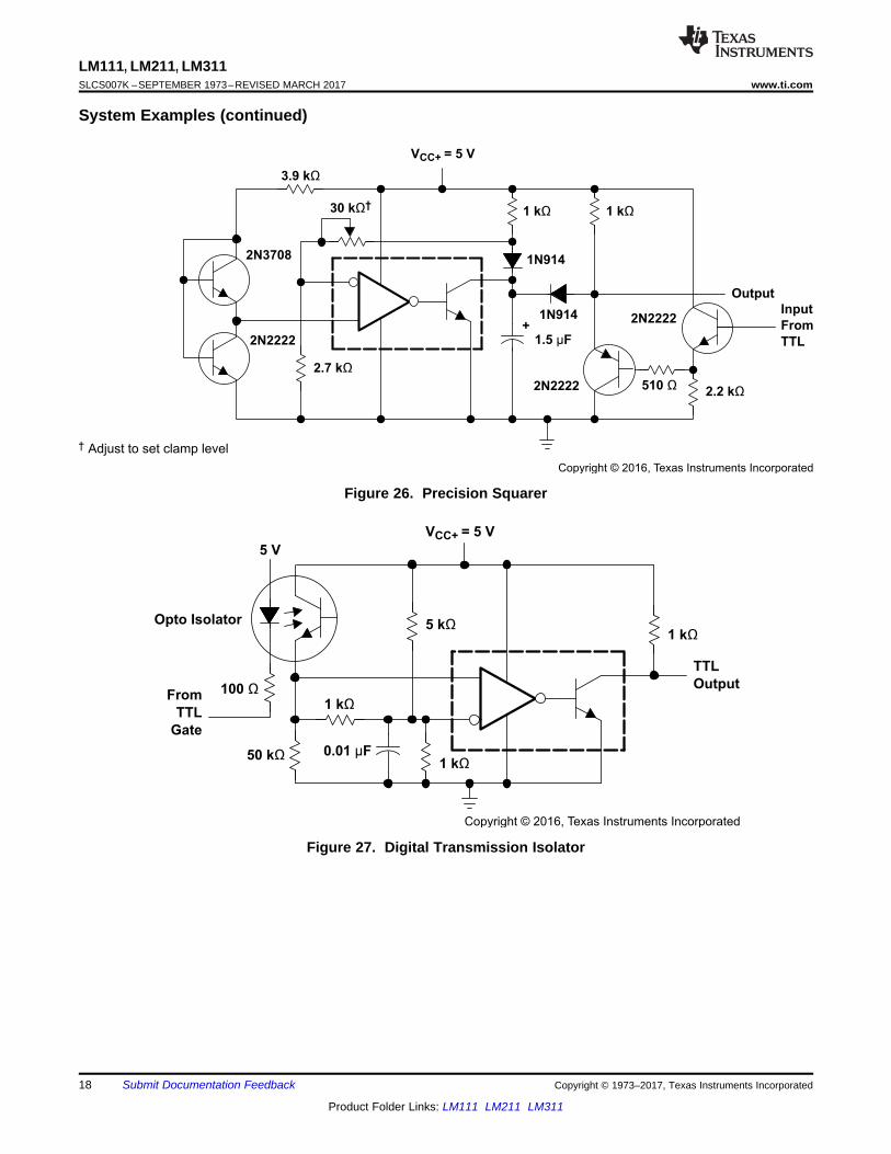
9.3 System ExamplesFigure 16 through Figure 33 show various applications for the LM111, LM211, and LM311 comparators.
Figure 16. 100-kHz Free-Running Multivibrator
1 kΩ
BAL/STRB
TTL
Strobe 2N2222
Copyright © 2016, Texas Instruments Incorporated
3 kΩ
3 kΩ
VCC+
BALANCEBAL/
STRB
Copyright © 2016, Texas Instruments Incorporated
15
LM111, LM211, LM311www.ti.com SLCS007K –SEPTEMBER 1973–REVISED MARCH 2017
Product Folder Links: LM111 LM211 LM311
Submit Documentation FeedbackCopyright © 1973–2017, Texas Instruments Incorporated
System Examples (continued)
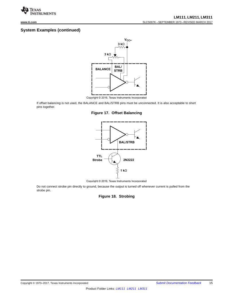
If offset balancing is not used, the BALANCE and BAL/STRB pins must be unconnected. It is also acceptable to shortpins together.
Figure 17. Offset Balancing
Do not connect strobe pin directly to ground, because the output is turned off whenever current is pulled from thestrobe pin.
Figure 18. Strobing
0.1 Fµ
50 kΩ
VCC+
2 kΩ100 kΩ
100 kΩ
100 kHz
Output
10 pF
Copyright © 2016, Texas Instruments Incorporated
5 V
2 kΩ4.5 kΩ
1 kΩ
Magnetic
Transducer
Output
to TTL
Copyright © 2016, Texas Instruments Incorporated
† Resistor values shown are for a 0- to 30-V logic swing and a 15-V threshold.‡ May be added to control speed and reduce susceptibility to noise spikes
5 V
1 kΩ
240 kΩ
82 kΩ
47 kΩ
82 kΩ
Output to TTLInput
‡
†
Copyright © 2016, Texas Instruments Incorporated
16
LM111, LM211, LM311SLCS007K –SEPTEMBER 1973–REVISED MARCH 2017 www.ti.com
Product Folder Links: LM111 LM211 LM311
Submit Documentation Feedback Copyright © 1973–2017, Texas Instruments Incorporated
System Examples (continued)
Figure 19. TTL Interface With High-Level Logic
Figure 20. Detector for Magnetic Transducer Figure 21. 100-kHz Crystal Oscillator
500 Ω3.9 kΩ
10 kΩ
1.5 µF+
VCC+
Output
2N2222
2N3708
1 kΩ
Copyright © 2016, Texas Instruments Incorporated
3 kΩ
3 kΩ
VCC+ = 5 V
Input
10 kΩ
VCC− = −10 V
Output
to MOS
BAL/
STRBBALANCE
Copyright © 2016, Texas Instruments Incorporated
† Typical input current is 50 pA with inputs strobed off.
VCC+
1 kΩ
From D/A Network
0.1 µF
Sample
Analog
Input
2N2222
†
TTL
Strobe
BAL/STRBBALANCE
Copyright © 2016, Texas Instruments Incorporated
Input
22 kΩ
Output
VCC+
Copyright © 2016, Texas Instruments Incorporated
17
LM111, LM211, LM311www.ti.com SLCS007K –SEPTEMBER 1973–REVISED MARCH 2017
Product Folder Links: LM111 LM211 LM311
Submit Documentation FeedbackCopyright © 1973–2017, Texas Instruments Incorporated
System Examples (continued)
Figure 22. Comparator and Solenoid Driver Figure 23. Strobing Both Input and Output StagesSimultaneously
Figure 24. Low-Voltage Adjustable ReferenceSupply
Figure 25. Zero-Crossing Detector Driving MOSLogic
5 kΩ
0.01 µF
TTL
Output
1 kΩ
1 kΩ
1 kΩ
100 ΩFrom
TTL
Gate
50 kΩ
Opto Isolator
5 V
VCC+ = 5 V
Copyright © 2016, Texas Instruments Incorporated
† Adjust to set clamp level
3.9 kΩ
30 kن
1.5 µF+
VCC+ = 5 V
Input
From
TTL2N2222
2N3708
Output
510 Ω
1 kΩ 1 kΩ
2N2222
2N2222
2.2 kΩ
1N914
1N914
2.7 kΩ
Copyright © 2016, Texas Instruments Incorporated
18
LM111, LM211, LM311SLCS007K –SEPTEMBER 1973–REVISED MARCH 2017 www.ti.com
Product Folder Links: LM111 LM211 LM311
Submit Documentation Feedback Copyright © 1973–2017, Texas Instruments Incorporated
System Examples (continued)
Figure 26. Precision Squarer
Figure 27. Digital Transmission Isolator
15 Fµ+
10 kΩ
1 MΩ
VCC+ = 15 V
TL081
OutputInput
VCC− = −15 V
2 kΩ +
−
Copyright © 2016, Texas Instruments Incorporated
1.5 Fµ+
10 kΩ
2 kΩ
VCC+ = 15 V
TL081
Output
Input
1 MΩ
VCC− = −15 V
−
+
Copyright © 2016, Texas Instruments Incorporated
19
LM111, LM211, LM311www.ti.com SLCS007K –SEPTEMBER 1973–REVISED MARCH 2017
Product Folder Links: LM111 LM211 LM311
Submit Documentation FeedbackCopyright © 1973–2017, Texas Instruments Incorporated
System Examples (continued)
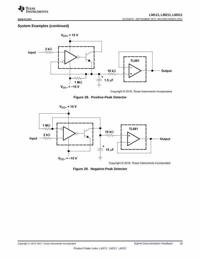
Figure 28. Positive-Peak Detector
Figure 29. Negative-Peak Detector
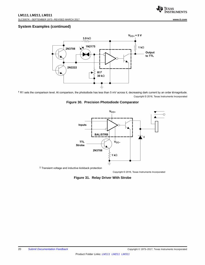
‡ Transient voltage and inductive kickback protection
2N3708
VCC+
Inputs
TTL
Strobe
VCC−
‡
1 kΩ
BAL/STRB
Copyright © 2016, Texas Instruments Incorporated
† R1 sets the comparison level. At comparison, the photodiode has less than 5 mV across it, decreasing dark current by an order of magnitude.
2N2222
2N3708
R1†
30 kΩ
3.9 kΩ
1 kΩ
Output
to TTL
VCC+ = 5 V
1N2175
Copyright © 2016, Texas Instruments Incorporated
20
LM111, LM211, LM311SLCS007K –SEPTEMBER 1973–REVISED MARCH 2017 www.ti.com
Product Folder Links: LM111 LM211 LM311
Submit Documentation Feedback Copyright © 1973–2017, Texas Instruments Incorporated
System Examples (continued)
Figure 30. Precision Photodiode Comparator
Figure 31. Relay Driver With Strobe
V+
0.22 Fµ
300 kΩ
620 Ω
1
VCC−
2
VCC−
620 Ω
620 Ω
620 Ω
620 Ω
620 Ω
39 kΩ
510 Ω
510 Ω
15 kΩ
15 kΩ
39 kΩ
300 kΩ
Outputs
VCC+
Input
Reference
BAL/STRB
BAL/STRB
Copyright © 2016, Texas Instruments Incorporated
300 Ω
VCC+
VCC−
100 kΩ Output
100 kΩ
47 Ω
10 kΩ
620 Ω
Input
0.1 µF 300 Ω 620 Ω
1
2
BAL/STRB
BAL/STRB
Copyright © 2016, Texas Instruments Incorporated
21
LM111, LM211, LM311www.ti.com SLCS007K –SEPTEMBER 1973–REVISED MARCH 2017
Product Folder Links: LM111 LM211 LM311
Submit Documentation FeedbackCopyright © 1973–2017, Texas Instruments Incorporated
System Examples (continued)
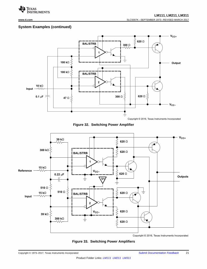
Figure 32. Switching Power Amplifier
Figure 33. Switching Power Amplifiers
EMIT OUT 1
1INí
21IN+
3
VCC- 4
8 VCC+
7 COL OUT
6 BAL/STROB
5 BALANCE
0.1µF
Ground
Bypass
Capacitor
Negative Supply or Ground
Positive Supply
0.1µF
Ground
Only needed
for dual power
supplies
Copyright © 2016, Texas Instruments Incorporated
22
LM111, LM211, LM311SLCS007K –SEPTEMBER 1973–REVISED MARCH 2017 www.ti.com
Product Folder Links: LM111 LM211 LM311
Submit Documentation Feedback Copyright © 1973–2017, Texas Instruments Incorporated
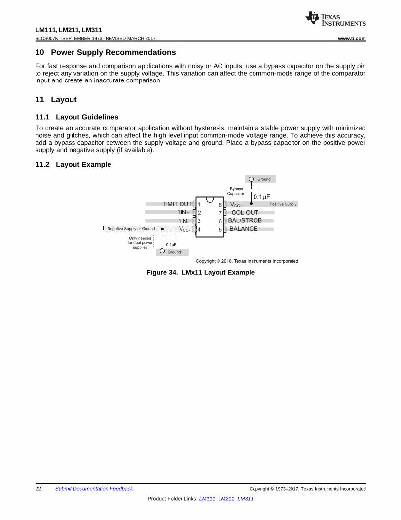
10 Power Supply RecommendationsFor fast response and comparison applications with noisy or AC inputs, use a bypass capacitor on the supply pinto reject any variation on the supply voltage. This variation can affect the common-mode range of the comparatorinput and create an inaccurate comparison.
11 Layout
11.1 Layout GuidelinesTo create an accurate comparator application without hysteresis, maintain a stable power supply with minimizednoise and glitches, which can affect the high level input common-mode voltage range. To achieve this accuracy,add a bypass capacitor between the supply voltage and ground. Place a bypass capacitor on the positive powersupply and negative supply (if available).
11.2 Layout Example
Figure 34. LMx11 Layout Example
23
LM111, LM211, LM311www.ti.com SLCS007K –SEPTEMBER 1973–REVISED MARCH 2017
Product Folder Links: LM111 LM211 LM311
Submit Documentation FeedbackCopyright © 1973–2017, Texas Instruments Incorporated
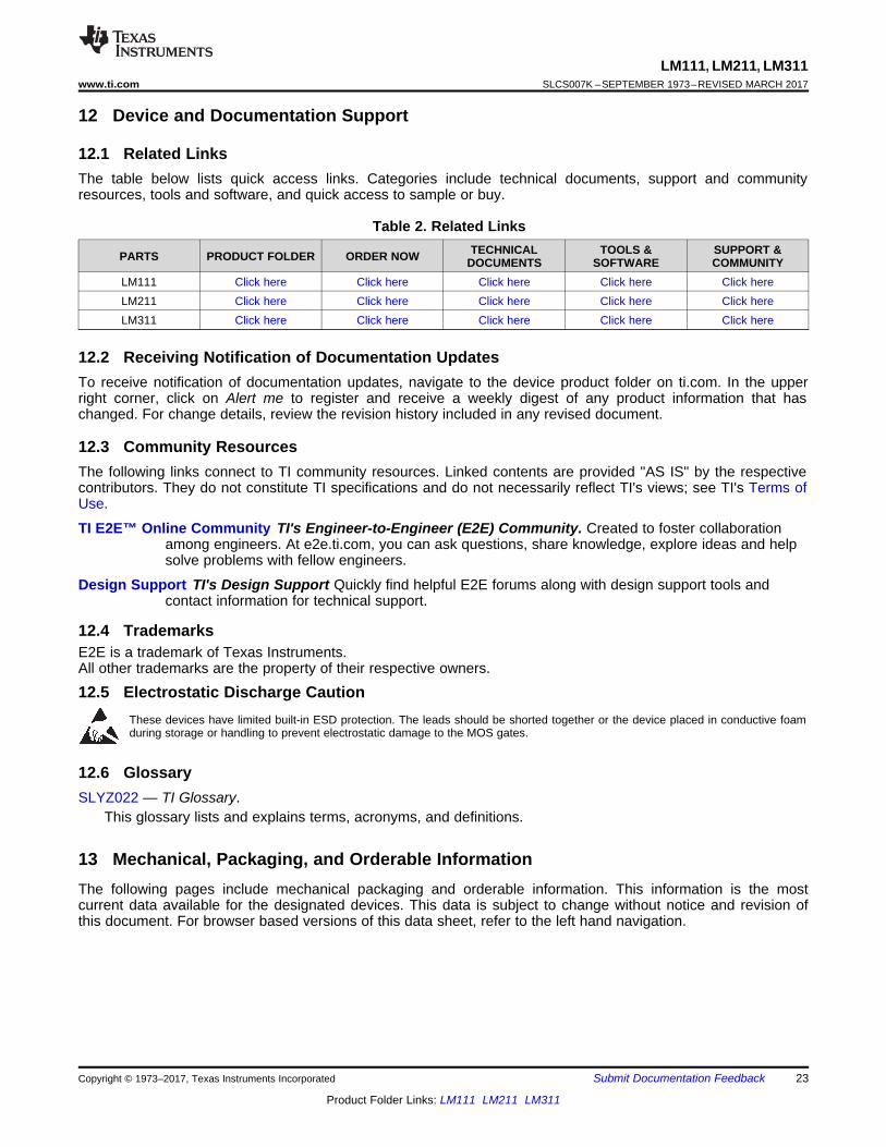
12 Device and Documentation Support
12.1 Related LinksThe table below lists quick access links. Categories include technical documents, support and communityresources, tools and software, and quick access to sample or buy.
Table 2. Related Links
PARTS PRODUCT FOLDER ORDER NOW TECHNICALDOCUMENTS
TOOLS &SOFTWARE
SUPPORT &COMMUNITY
LM111 Click here Click here Click here Click here Click hereLM211 Click here Click here Click here Click here Click hereLM311 Click here Click here Click here Click here Click here
12.2 Receiving Notification of Documentation UpdatesTo receive notification of documentation updates, navigate to the device product folder on ti.com. In the upperright corner, click on Alert me to register and receive a weekly digest of any product information that haschanged. For change details, review the revision history included in any revised document.
12.3 Community ResourcesThe following links connect to TI community resources. Linked contents are provided "AS IS" by the respectivecontributors. They do not constitute TI specifications and do not necessarily reflect TI's views; see TI's Terms ofUse.
TI E2E™ Online Community TI's Engineer-to-Engineer (E2E) Community. Created to foster collaborationamong engineers. At e2e.ti.com, you can ask questions, share knowledge, explore ideas and helpsolve problems with fellow engineers.
Design Support TI's Design Support Quickly find helpful E2E forums along with design support tools andcontact information for technical support.
12.4 TrademarksE2E is a trademark of Texas Instruments.All other trademarks are the property of their respective owners.
12.5 Electrostatic Discharge CautionThese devices have limited built-in ESD protection. The leads should be shorted together or the device placed in conductive foamduring storage or handling to prevent electrostatic damage to the MOS gates.
12.6 GlossarySLYZ022 — TI Glossary.
This glossary lists and explains terms, acronyms, and definitions.
13 Mechanical, Packaging, and Orderable InformationThe following pages include mechanical packaging and orderable information. This information is the mostcurrent data available for the designated devices. This data is subject to change without notice and revision ofthis document. For browser based versions of this data sheet, refer to the left hand navigation.
PACKAGE OPTION ADDENDUM
www.ti.com 29-Jun-2017
Addendum-Page 1
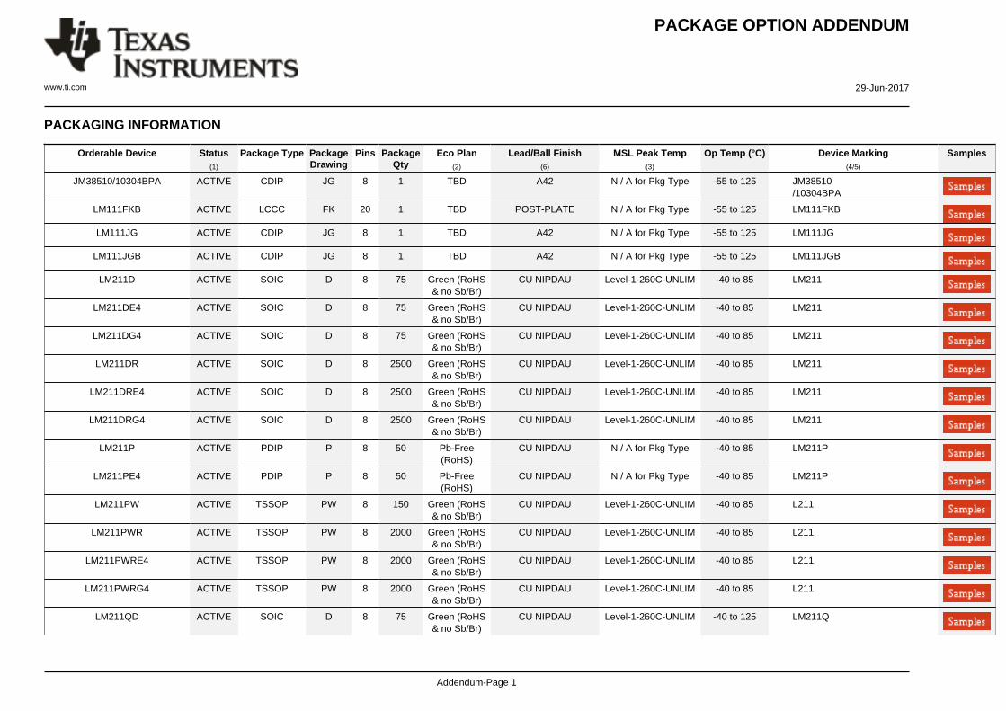
PACKAGING INFORMATION
Orderable Device Status(1)
Package Type PackageDrawing
Pins PackageQty
Eco Plan(2)
Lead/Ball Finish(6)
MSL Peak Temp(3)
Op Temp (°C) Device Marking(4/5)
Samples
JM38510/10304BPA ACTIVE CDIP JG 8 1 TBD A42 N / A for Pkg Type -55 to 125 JM38510/10304BPA
LM111FKB ACTIVE LCCC FK 20 1 TBD POST-PLATE N / A for Pkg Type -55 to 125 LM111FKB
LM111JG ACTIVE CDIP JG 8 1 TBD A42 N / A for Pkg Type -55 to 125 LM111JG
LM111JGB ACTIVE CDIP JG 8 1 TBD A42 N / A for Pkg Type -55 to 125 LM111JGB
LM211D ACTIVE SOIC D 8 75 Green (RoHS& no Sb/Br)
CU NIPDAU Level-1-260C-UNLIM -40 to 85 LM211
LM211DE4 ACTIVE SOIC D 8 75 Green (RoHS& no Sb/Br)
CU NIPDAU Level-1-260C-UNLIM -40 to 85 LM211
LM211DG4 ACTIVE SOIC D 8 75 Green (RoHS& no Sb/Br)
CU NIPDAU Level-1-260C-UNLIM -40 to 85 LM211
LM211DR ACTIVE SOIC D 8 2500 Green (RoHS& no Sb/Br)
CU NIPDAU Level-1-260C-UNLIM -40 to 85 LM211
LM211DRE4 ACTIVE SOIC D 8 2500 Green (RoHS& no Sb/Br)
CU NIPDAU Level-1-260C-UNLIM -40 to 85 LM211
LM211DRG4 ACTIVE SOIC D 8 2500 Green (RoHS& no Sb/Br)
CU NIPDAU Level-1-260C-UNLIM -40 to 85 LM211
LM211P ACTIVE PDIP P 8 50 Pb-Free(RoHS)
CU NIPDAU N / A for Pkg Type -40 to 85 LM211P
LM211PE4 ACTIVE PDIP P 8 50 Pb-Free(RoHS)
CU NIPDAU N / A for Pkg Type -40 to 85 LM211P
LM211PW ACTIVE TSSOP PW 8 150 Green (RoHS& no Sb/Br)
CU NIPDAU Level-1-260C-UNLIM -40 to 85 L211
LM211PWR ACTIVE TSSOP PW 8 2000 Green (RoHS& no Sb/Br)
CU NIPDAU Level-1-260C-UNLIM -40 to 85 L211
LM211PWRE4 ACTIVE TSSOP PW 8 2000 Green (RoHS& no Sb/Br)
CU NIPDAU Level-1-260C-UNLIM -40 to 85 L211
LM211PWRG4 ACTIVE TSSOP PW 8 2000 Green (RoHS& no Sb/Br)
CU NIPDAU Level-1-260C-UNLIM -40 to 85 L211
LM211QD ACTIVE SOIC D 8 75 Green (RoHS& no Sb/Br)
CU NIPDAU Level-1-260C-UNLIM -40 to 125 LM211Q
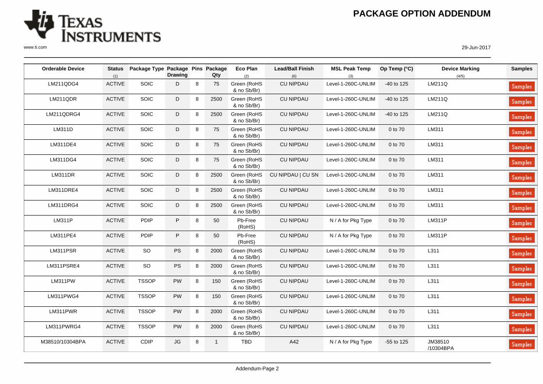
PACKAGE OPTION ADDENDUM
www.ti.com 29-Jun-2017
Addendum-Page 2
Orderable Device Status(1)
Package Type PackageDrawing
Pins PackageQty
Eco Plan(2)
Lead/Ball Finish(6)
MSL Peak Temp(3)
Op Temp (°C) Device Marking(4/5)
Samples
LM211QDG4 ACTIVE SOIC D 8 75 Green (RoHS& no Sb/Br)
CU NIPDAU Level-1-260C-UNLIM -40 to 125 LM211Q
LM211QDR ACTIVE SOIC D 8 2500 Green (RoHS& no Sb/Br)
CU NIPDAU Level-1-260C-UNLIM -40 to 125 LM211Q
LM211QDRG4 ACTIVE SOIC D 8 2500 Green (RoHS& no Sb/Br)
CU NIPDAU Level-1-260C-UNLIM -40 to 125 LM211Q
LM311D ACTIVE SOIC D 8 75 Green (RoHS& no Sb/Br)
CU NIPDAU Level-1-260C-UNLIM 0 to 70 LM311
LM311DE4 ACTIVE SOIC D 8 75 Green (RoHS& no Sb/Br)
CU NIPDAU Level-1-260C-UNLIM 0 to 70 LM311
LM311DG4 ACTIVE SOIC D 8 75 Green (RoHS& no Sb/Br)
CU NIPDAU Level-1-260C-UNLIM 0 to 70 LM311
LM311DR ACTIVE SOIC D 8 2500 Green (RoHS& no Sb/Br)
CU NIPDAU | CU SN Level-1-260C-UNLIM 0 to 70 LM311
LM311DRE4 ACTIVE SOIC D 8 2500 Green (RoHS& no Sb/Br)
CU NIPDAU Level-1-260C-UNLIM 0 to 70 LM311
LM311DRG4 ACTIVE SOIC D 8 2500 Green (RoHS& no Sb/Br)
CU NIPDAU Level-1-260C-UNLIM 0 to 70 LM311
LM311P ACTIVE PDIP P 8 50 Pb-Free(RoHS)
CU NIPDAU N / A for Pkg Type 0 to 70 LM311P
LM311PE4 ACTIVE PDIP P 8 50 Pb-Free(RoHS)
CU NIPDAU N / A for Pkg Type 0 to 70 LM311P
LM311PSR ACTIVE SO PS 8 2000 Green (RoHS& no Sb/Br)
CU NIPDAU Level-1-260C-UNLIM 0 to 70 L311
LM311PSRE4 ACTIVE SO PS 8 2000 Green (RoHS& no Sb/Br)
CU NIPDAU Level-1-260C-UNLIM 0 to 70 L311
LM311PW ACTIVE TSSOP PW 8 150 Green (RoHS& no Sb/Br)
CU NIPDAU Level-1-260C-UNLIM 0 to 70 L311
LM311PWG4 ACTIVE TSSOP PW 8 150 Green (RoHS& no Sb/Br)
CU NIPDAU Level-1-260C-UNLIM 0 to 70 L311
LM311PWR ACTIVE TSSOP PW 8 2000 Green (RoHS& no Sb/Br)
CU NIPDAU Level-1-260C-UNLIM 0 to 70 L311
LM311PWRG4 ACTIVE TSSOP PW 8 2000 Green (RoHS& no Sb/Br)
CU NIPDAU Level-1-260C-UNLIM 0 to 70 L311
M38510/10304BPA ACTIVE CDIP JG 8 1 TBD A42 N / A for Pkg Type -55 to 125 JM38510/10304BPA
PACKAGE OPTION ADDENDUM
www.ti.com 29-Jun-2017
Addendum-Page 3
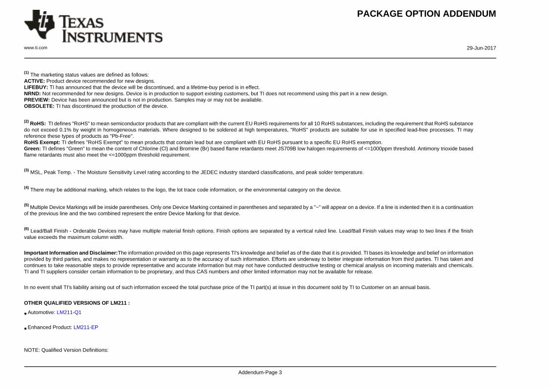
(1) The marketing status values are defined as follows:ACTIVE: Product device recommended for new designs.LIFEBUY: TI has announced that the device will be discontinued, and a lifetime-buy period is in effect.NRND: Not recommended for new designs. Device is in production to support existing customers, but TI does not recommend using this part in a new design.PREVIEW: Device has been announced but is not in production. Samples may or may not be available.OBSOLETE: TI has discontinued the production of the device.
(2) RoHS: TI defines "RoHS" to mean semiconductor products that are compliant with the current EU RoHS requirements for all 10 RoHS substances, including the requirement that RoHS substancedo not exceed 0.1% by weight in homogeneous materials. Where designed to be soldered at high temperatures, "RoHS" products are suitable for use in specified lead-free processes. TI mayreference these types of products as "Pb-Free".RoHS Exempt: TI defines "RoHS Exempt" to mean products that contain lead but are compliant with EU RoHS pursuant to a specific EU RoHS exemption.Green: TI defines "Green" to mean the content of Chlorine (Cl) and Bromine (Br) based flame retardants meet JS709B low halogen requirements of <=1000ppm threshold. Antimony trioxide basedflame retardants must also meet the <=1000ppm threshold requirement.
(3) MSL, Peak Temp. - The Moisture Sensitivity Level rating according to the JEDEC industry standard classifications, and peak solder temperature.
(4) There may be additional marking, which relates to the logo, the lot trace code information, or the environmental category on the device.
(5) Multiple Device Markings will be inside parentheses. Only one Device Marking contained in parentheses and separated by a "~" will appear on a device. If a line is indented then it is a continuationof the previous line and the two combined represent the entire Device Marking for that device.
(6) Lead/Ball Finish - Orderable Devices may have multiple material finish options. Finish options are separated by a vertical ruled line. Lead/Ball Finish values may wrap to two lines if the finishvalue exceeds the maximum column width.
Important Information and Disclaimer:The information provided on this page represents TI's knowledge and belief as of the date that it is provided. TI bases its knowledge and belief on informationprovided by third parties, and makes no representation or warranty as to the accuracy of such information. Efforts are underway to better integrate information from third parties. TI has taken andcontinues to take reasonable steps to provide representative and accurate information but may not have conducted destructive testing or chemical analysis on incoming materials and chemicals.TI and TI suppliers consider certain information to be proprietary, and thus CAS numbers and other limited information may not be available for release.
In no event shall TI's liability arising out of such information exceed the total purchase price of the TI part(s) at issue in this document sold by TI to Customer on an annual basis.
OTHER QUALIFIED VERSIONS OF LM211 :
• Automotive: LM211-Q1
• Enhanced Product: LM211-EP
NOTE: Qualified Version Definitions:
PACKAGE OPTION ADDENDUM
www.ti.com 29-Jun-2017
Addendum-Page 4
• Automotive - Q100 devices qualified for high-reliability automotive applications targeting zero defects
• Enhanced Product - Supports Defense, Aerospace and Medical Applications
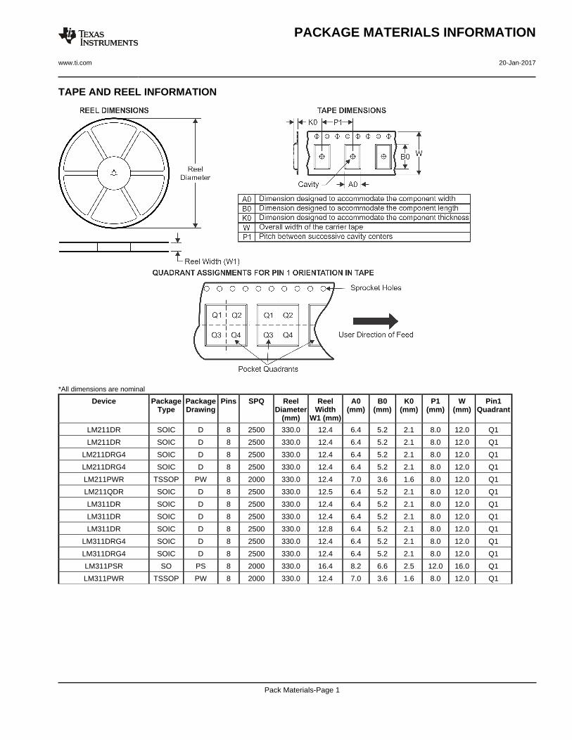
TAPE AND REEL INFORMATION
*All dimensions are nominal
Device PackageType
PackageDrawing
Pins SPQ ReelDiameter
(mm)
ReelWidth
W1 (mm)
A0(mm)
B0(mm)
K0(mm)
P1(mm)
W(mm)
Pin1Quadrant
LM211DR SOIC D 8 2500 330.0 12.4 6.4 5.2 2.1 8.0 12.0 Q1
LM211DR SOIC D 8 2500 330.0 12.4 6.4 5.2 2.1 8.0 12.0 Q1
LM211DRG4 SOIC D 8 2500 330.0 12.4 6.4 5.2 2.1 8.0 12.0 Q1
LM211DRG4 SOIC D 8 2500 330.0 12.4 6.4 5.2 2.1 8.0 12.0 Q1
LM211PWR TSSOP PW 8 2000 330.0 12.4 7.0 3.6 1.6 8.0 12.0 Q1
LM211QDR SOIC D 8 2500 330.0 12.5 6.4 5.2 2.1 8.0 12.0 Q1
LM311DR SOIC D 8 2500 330.0 12.4 6.4 5.2 2.1 8.0 12.0 Q1
LM311DR SOIC D 8 2500 330.0 12.4 6.4 5.2 2.1 8.0 12.0 Q1
LM311DR SOIC D 8 2500 330.0 12.8 6.4 5.2 2.1 8.0 12.0 Q1
LM311DRG4 SOIC D 8 2500 330.0 12.4 6.4 5.2 2.1 8.0 12.0 Q1
LM311DRG4 SOIC D 8 2500 330.0 12.4 6.4 5.2 2.1 8.0 12.0 Q1
LM311PSR SO PS 8 2000 330.0 16.4 8.2 6.6 2.5 12.0 16.0 Q1
LM311PWR TSSOP PW 8 2000 330.0 12.4 7.0 3.6 1.6 8.0 12.0 Q1
PACKAGE MATERIALS INFORMATION
www.ti.com 20-Jan-2017
Pack Materials-Page 1
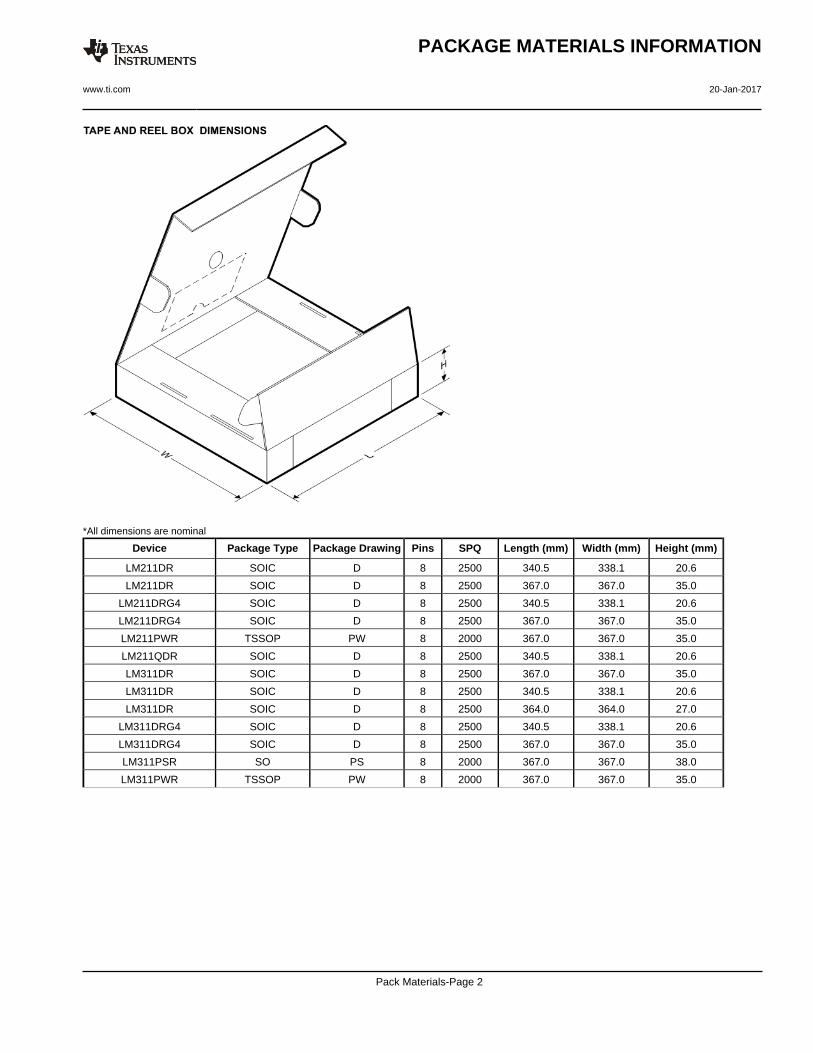
*All dimensions are nominal
Device Package Type Package Drawing Pins SPQ Length (mm) Width (mm) Height (mm)
LM211DR SOIC D 8 2500 340.5 338.1 20.6
LM211DR SOIC D 8 2500 367.0 367.0 35.0
LM211DRG4 SOIC D 8 2500 340.5 338.1 20.6
LM211DRG4 SOIC D 8 2500 367.0 367.0 35.0
LM211PWR TSSOP PW 8 2000 367.0 367.0 35.0
LM211QDR SOIC D 8 2500 340.5 338.1 20.6
LM311DR SOIC D 8 2500 367.0 367.0 35.0
LM311DR SOIC D 8 2500 340.5 338.1 20.6
LM311DR SOIC D 8 2500 364.0 364.0 27.0
LM311DRG4 SOIC D 8 2500 340.5 338.1 20.6
LM311DRG4 SOIC D 8 2500 367.0 367.0 35.0
LM311PSR SO PS 8 2000 367.0 367.0 38.0
LM311PWR TSSOP PW 8 2000 367.0 367.0 35.0
PACKAGE MATERIALS INFORMATION
www.ti.com 20-Jan-2017
Pack Materials-Page 2
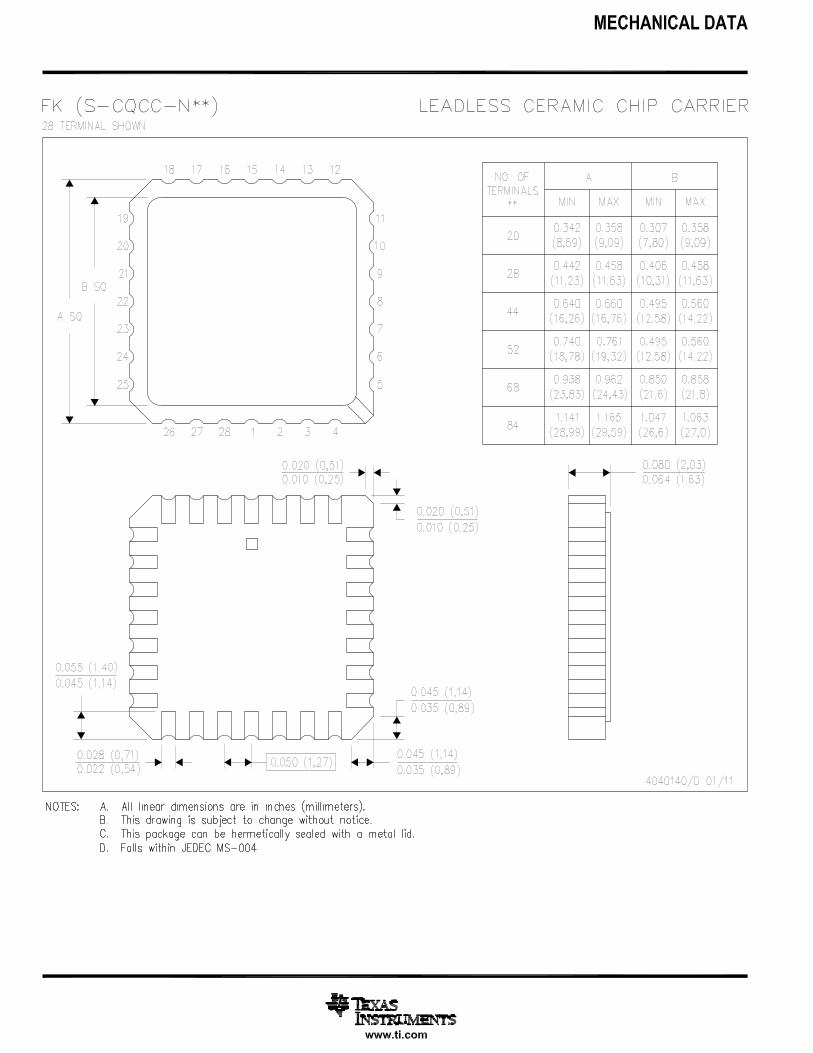
MECHANICAL DATA
MCER001A – JANUARY 1995 – REVISED JANUARY 1997
POST OFFICE BOX 655303 • DALLAS, TEXAS 75265
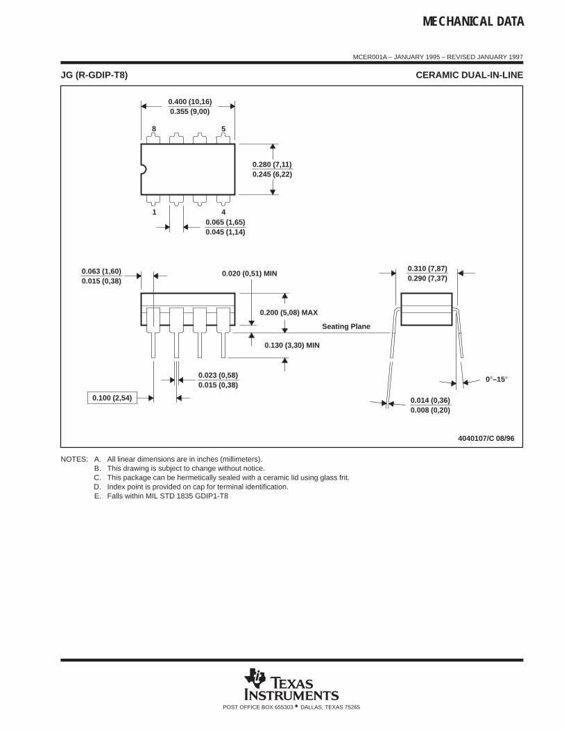
JG (R-GDIP-T8) CERAMIC DUAL-IN-LINE
0.310 (7,87)0.290 (7,37)
0.014 (0,36)0.008 (0,20)
Seating Plane
4040107/C 08/96
5
40.065 (1,65)0.045 (1,14)
8
1
0.020 (0,51) MIN
0.400 (10,16)0.355 (9,00)
0.015 (0,38)0.023 (0,58)
0.063 (1,60)0.015 (0,38)
0.200 (5,08) MAX
0.130 (3,30) MIN
0.245 (6,22)0.280 (7,11)
0.100 (2,54)
0°–15°
NOTES: A. All linear dimensions are in inches (millimeters).B. This drawing is subject to change without notice.C. This package can be hermetically sealed with a ceramic lid using glass frit.D. Index point is provided on cap for terminal identification.E. Falls within MIL STD 1835 GDIP1-T8
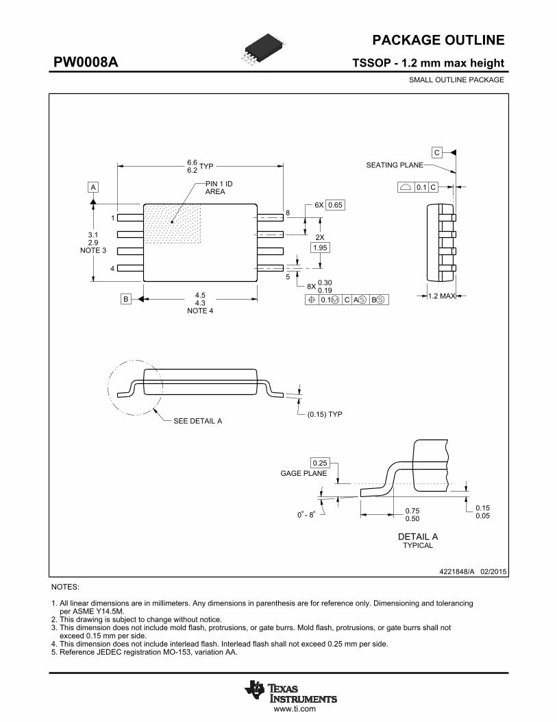
www.ti.com
PACKAGE OUTLINE
C
TYP6.66.2
1.2 MAX
6X 0.65
8X 0.300.19
2X1.95
0.150.05
(0.15) TYP
0 - 8
0.25GAGE PLANE
0.750.50
A
NOTE 3
3.12.9
BNOTE 4
4.54.3
4221848/A 02/2015
TSSOP - 1.2 mm max heightPW0008ASMALL OUTLINE PACKAGE
NOTES: 1. All linear dimensions are in millimeters. Any dimensions in parenthesis are for reference only. Dimensioning and tolerancing per ASME Y14.5M. 2. This drawing is subject to change without notice. 3. This dimension does not include mold flash, protrusions, or gate burrs. Mold flash, protrusions, or gate burrs shall not exceed 0.15 mm per side. 4. This dimension does not include interlead flash. Interlead flash shall not exceed 0.25 mm per side.5. Reference JEDEC registration MO-153, variation AA.
18
0.1 C A B
54
PIN 1 IDAREA
SEATING PLANE
0.1 C
SEE DETAIL A
DETAIL ATYPICAL
SCALE 2.800
www.ti.com
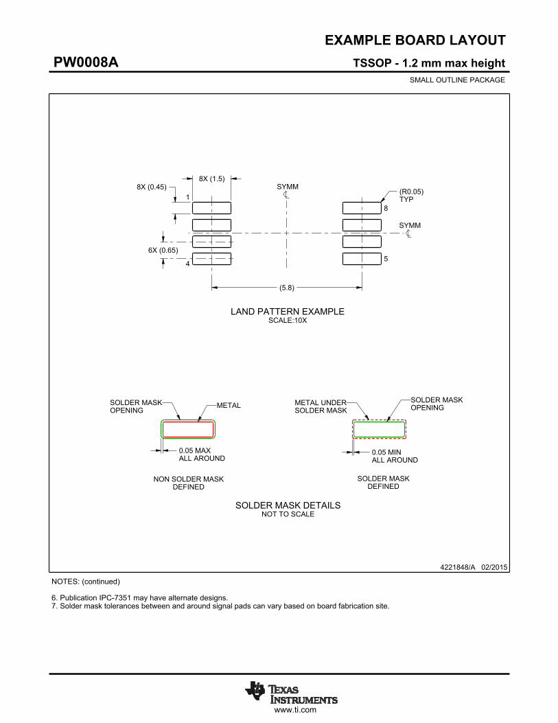
EXAMPLE BOARD LAYOUT
(5.8)
0.05 MAXALL AROUND
0.05 MINALL AROUND
8X (1.5)8X (0.45)
6X (0.65)
(R )TYP
0.05
4221848/A 02/2015
TSSOP - 1.2 mm max heightPW0008ASMALL OUTLINE PACKAGE
SYMM
SYMM
LAND PATTERN EXAMPLESCALE:10X
1
45
8
NOTES: (continued) 6. Publication IPC-7351 may have alternate designs. 7. Solder mask tolerances between and around signal pads can vary based on board fabrication site.
METALSOLDER MASKOPENING
NON SOLDER MASKDEFINED
SOLDER MASK DETAILSNOT TO SCALE
SOLDER MASKOPENING
METAL UNDERSOLDER MASK
SOLDER MASKDEFINED
www.ti.com
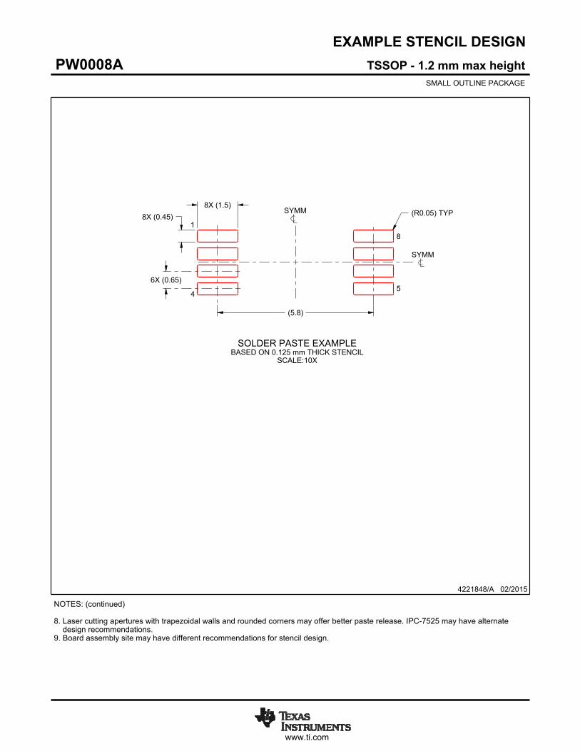
EXAMPLE STENCIL DESIGN
(5.8)
6X (0.65)
8X (0.45)8X (1.5)
(R ) TYP0.05
4221848/A 02/2015
TSSOP - 1.2 mm max heightPW0008ASMALL OUTLINE PACKAGE
NOTES: (continued) 8. Laser cutting apertures with trapezoidal walls and rounded corners may offer better paste release. IPC-7525 may have alternate design recommendations. 9. Board assembly site may have different recommendations for stencil design.
SYMM
SYMM
1
45
8
SOLDER PASTE EXAMPLEBASED ON 0.125 mm THICK STENCIL
SCALE:10X
IMPORTANT NOTICE
Texas Instruments Incorporated (TI) reserves the right to make corrections, enhancements, improvements and other changes to itssemiconductor products and services per JESD46, latest issue, and to discontinue any product or service per JESD48, latest issue. Buyersshould obtain the latest relevant information before placing orders and should verify that such information is current and complete.TI’s published terms of sale for semiconductor products (http://www.ti.com/sc/docs/stdterms.htm) apply to the sale of packaged integratedcircuit products that TI has qualified and released to market. Additional terms may apply to the use or sale of other types of TI products andservices.Reproduction of significant portions of TI information in TI data sheets is permissible only if reproduction is without alteration and isaccompanied by all associated warranties, conditions, limitations, and notices. TI is not responsible or liable for such reproduceddocumentation. Information of third parties may be subject to additional restrictions. Resale of TI products or services with statementsdifferent from or beyond the parameters stated by TI for that product or service voids all express and any implied warranties for theassociated TI product or service and is an unfair and deceptive business practice. TI is not responsible or liable for any such statements.Buyers and others who are developing systems that incorporate TI products (collectively, “Designers”) understand and agree that Designersremain responsible for using their independent analysis, evaluation and judgment in designing their applications and that Designers havefull and exclusive responsibility to assure the safety of Designers' applications and compliance of their applications (and of all TI productsused in or for Designers’ applications) with all applicable regulations, laws and other applicable requirements. Designer represents that, withrespect to their applications, Designer has all the necessary expertise to create and implement safeguards that (1) anticipate dangerousconsequences of failures, (2) monitor failures and their consequences, and (3) lessen the likelihood of failures that might cause harm andtake appropriate actions. Designer agrees that prior to using or distributing any applications that include TI products, Designer willthoroughly test such applications and the functionality of such TI products as used in such applications.TI’s provision of technical, application or other design advice, quality characterization, reliability data or other services or information,including, but not limited to, reference designs and materials relating to evaluation modules, (collectively, “TI Resources”) are intended toassist designers who are developing applications that incorporate TI products; by downloading, accessing or using TI Resources in anyway, Designer (individually or, if Designer is acting on behalf of a company, Designer’s company) agrees to use any particular TI Resourcesolely for this purpose and subject to the terms of this Notice.TI’s provision of TI Resources does not expand or otherwise alter TI’s applicable published warranties or warranty disclaimers for TIproducts, and no additional obligations or liabilities arise from TI providing such TI Resources. TI reserves the right to make corrections,enhancements, improvements and other changes to its TI Resources. TI has not conducted any testing other than that specificallydescribed in the published documentation for a particular TI Resource.Designer is authorized to use, copy and modify any individual TI Resource only in connection with the development of applications thatinclude the TI product(s) identified in such TI Resource. NO OTHER LICENSE, EXPRESS OR IMPLIED, BY ESTOPPEL OR OTHERWISETO ANY OTHER TI INTELLECTUAL PROPERTY RIGHT, AND NO LICENSE TO ANY TECHNOLOGY OR INTELLECTUAL PROPERTYRIGHT OF TI OR ANY THIRD PARTY IS GRANTED HEREIN, including but not limited to any patent right, copyright, mask work right, orother intellectual property right relating to any combination, machine, or process in which TI products or services are used. Informationregarding or referencing third-party products or services does not constitute a license to use such products or services, or a warranty orendorsement thereof. Use of TI Resources may require a license from a third party under the patents or other intellectual property of thethird party, or a license from TI under the patents or other intellectual property of TI.TI RESOURCES ARE PROVIDED “AS IS” AND WITH ALL FAULTS. TI DISCLAIMS ALL OTHER WARRANTIES ORREPRESENTATIONS, EXPRESS OR IMPLIED, REGARDING RESOURCES OR USE THEREOF, INCLUDING BUT NOT LIMITED TOACCURACY OR COMPLETENESS, TITLE, ANY EPIDEMIC FAILURE WARRANTY AND ANY IMPLIED WARRANTIES OFMERCHANTABILITY, FITNESS FOR A PARTICULAR PURPOSE, AND NON-INFRINGEMENT OF ANY THIRD PARTY INTELLECTUALPROPERTY RIGHTS. TI SHALL NOT BE LIABLE FOR AND SHALL NOT DEFEND OR INDEMNIFY DESIGNER AGAINST ANY CLAIM,INCLUDING BUT NOT LIMITED TO ANY INFRINGEMENT CLAIM THAT RELATES TO OR IS BASED ON ANY COMBINATION OFPRODUCTS EVEN IF DESCRIBED IN TI RESOURCES OR OTHERWISE. IN NO EVENT SHALL TI BE LIABLE FOR ANY ACTUAL,DIRECT, SPECIAL, COLLATERAL, INDIRECT, PUNITIVE, INCIDENTAL, CONSEQUENTIAL OR EXEMPLARY DAMAGES INCONNECTION WITH OR ARISING OUT OF TI RESOURCES OR USE THEREOF, AND REGARDLESS OF WHETHER TI HAS BEENADVISED OF THE POSSIBILITY OF SUCH DAMAGES.Unless TI has explicitly designated an individual product as meeting the requirements of a particular industry standard (e.g., ISO/TS 16949and ISO 26262), TI is not responsible for any failure to meet such industry standard requirements.Where TI specifically promotes products as facilitating functional safety or as compliant with industry functional safety standards, suchproducts are intended to help enable customers to design and create their own applications that meet applicable functional safety standardsand requirements. Using products in an application does not by itself establish any safety features in the application. Designers mustensure compliance with safety-related requirements and standards applicable to their applications. Designer may not use any TI products inlife-critical medical equipment unless authorized officers of the parties have executed a special contract specifically governing such use.Life-critical medical equipment is medical equipment where failure of such equipment would cause serious bodily injury or death (e.g., lifesupport, pacemakers, defibrillators, heart pumps, neurostimulators, and implantables). Such equipment includes, without limitation, allmedical devices identified by the U.S. Food and Drug Administration as Class III devices and equivalent classifications outside the U.S.TI may expressly designate certain products as completing a particular qualification (e.g., Q100, Military Grade, or Enhanced Product).Designers agree that it has the necessary expertise to select the product with the appropriate qualification designation for their applicationsand that proper product selection is at Designers’ own risk. Designers are solely responsible for compliance with all legal and regulatoryrequirements in connection with such selection.Designer will fully indemnify TI and its representatives against any damages, costs, losses, and/or liabilities arising out of Designer’s non-compliance with the terms and provisions of this Notice.
Mailing Address: Texas Instruments, Post Office Box 655303, Dallas, Texas 75265Copyright © 2017, Texas Instruments Incorporated
Top Related