


Languages
Pages
Legal


Lecture 9: Components of pPhase Locked Loop (PLL)
CSCE 6730
p ( )CSCE 6730
Advanced VLSI SystemsyInstructor: Saraju P. Mohanty, Ph. D.
NOTE: The figures, text etc included in slides are borrowed from various books,websites, authors pages, and other sources for academic purpose only. Theinstructor does not claim any originality.
1Advanced VLSI Systems

Lecture Outline
• Overall view of a Phase Locked LoopC t f PLL• Components of a PLL
• High Level System DesignC t i D i d P• Component - wise Design and PowerOptimization
• Mixed Signal System Analysis• Mixed-Signal System Analysis
2Advanced VLSI Systems

Phase Locked Loop• The first phase locked loop was proposed by a French scientist de
Bellescize in 1932
• Basic idea of working: reduction of phase difference between a locallygenerated signal and a reference signal by using feedback
• A Phase Locked Loop (PLL) circuit synchronizes to an input waveform withina selected frequency range, returning an output voltage proportional tovariations in the input frequencya a o s e pu eque cy
• Used to generate stable output frequency signals from a fixed low-frequencysignalg
• Two types: Analog and Digital– Analog PLLs are extensively used in communication systems as they maintain aAnalog PLLs are extensively used in communication systems as they maintain a
linear relationship between the input and the output– Digital PLLs are suitable for synchronization of digital signals, clock recovery from
encoded digital data streams and other digital applications
3Advanced VLSI Systems

Phase Locked Loop (contd..)
• Three fundamental purposes of a PLL– Demodulator: matched filter operating as a coherent detector– Tracker of a carrier or synchronizing signal: narrow-band filter for
removing noise from the signal and regenerating a clean replica of thesignal
– Frequency synthesizer: oscillator is locked to a multiple of an accuratereference frequency
• The components of a Phase Locked Loop are:Phase Detector– Phase Detector
– Charge Pump– Loop Filter– Voltage Controlled Oscillator– Frequency Divider
4Advanced VLSI Systems

Phase Locked Loop (contd..)Reference Signal
Output Signal
Phase VoltagePhaseDetector Charge Pump Loop Filter Controlled
Oscillator
Frequency Divider
Phase detector and charge pump together form the error detector blockerror detector block
5Advanced VLSI Systems

High Level System Design• Behavioral-modeling languages like Verilog-AMS and Verilog-A are very
important tools for a top-down design methodology for circuit designers
• Provide validation of the overall system
• Better performance at a higher speed
• Verilog A: C like behavioral description language for circuit designing• Verilog-A: C like behavioral description language for circuit designing
• Non-ideal characteristic behavior description
6Advanced VLSI Systems

Voltage Controlled Oscillator
• Oscillators are used to create a periodic logic or analog signal with a stablep g g gand predictable frequency
• Types of oscillators:– LC oscillators - oscillates by charging and discharging a capacitor
through an inductor– Crystal oscillators
Ring oscillators– Ring oscillators
• VCO is an electronic oscillator specifically designed to be controlled inoscillation frequency by a voltage inputq y y g p
• Current starved VCO is used
7Advanced VLSI Systems
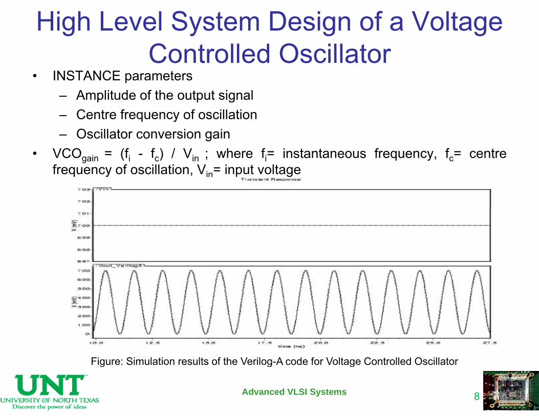
High Level System Design of a Voltage Controlled OscillatorControlled Oscillator
• INSTANCE parameters– Amplitude of the output signal– Centre frequency of oscillation– Oscillator conversion gain
• VCOgain = (fi - fc) / Vin ; where fi= instantaneous frequency, fc= centreVCOgain (fi fc) / Vin ; where fi instantaneous frequency, fc centrefrequency of oscillation, Vin= input voltage
Figure: Simulation results of the Verilog A code for Voltage Controlled OscillatorFigure: Simulation results of the Verilog-A code for Voltage Controlled Oscillator
8Advanced VLSI Systems

Current Starved Voltage Controlled Oscillatorg
C t St d VCO i f• Current Starved VCO comprises of– Odd numbered chain of inverters– Two input stage transistors => limit current flow to the inverterp g
• Frequency of oscillation (fo) depends onNumber of inverters (N)– Number of inverters (N)
– Size of the transistor (W/L)– Current flowing through the inverter (Iinv) which is dependent on the input
l (V )voltage (Vdd)– So, fo = Iinv / (N*CTOT*Vdd); where CTOT is the total capacitance of the
inverter transistors
9Advanced VLSI Systems

Transistor Level Diagram of a VCO
10Advanced VLSI Systems

VCO Equations
Frequency of Oscillation
where
and
11Advanced VLSI Systems

Analog Design and Simulation Results of the VCOof the VCO
Fig: Simulation waveform of the analog VCO
Fig: Transistor level circuit diagram of the VCO
Fig: Voltage versus Frequency response
12Advanced VLSI Systems

Experimental Results: Power Analysis on VCOVCO
Average power and Leakage power are calculatedCalculator option in Cadence Spectre was usedCalculator option in Cadence Spectre was used
Table: Gate leakage and dynamic current for individual transistors in the VCO for an input voltage of 0 7VTable: Gate leakage and dynamic current for individual transistors in the VCO for an input voltage of 0.7V
13Advanced VLSI Systems

Design of ExperimentsDesign of Experiments• Full factorial method
Ch i t t t di d ith h i i t– Change in output studied with change in input– Two values for each input; one is considered as ‘+1’ and the other as ‘–1’– Taguchi L8 design matrix
Eight different combinations => eight experiments– Eight different combinations => eight experiments– Output responses are tabulated– Average values of output responses and then ∆ (effect) values are
calculated and then the average value over each column of ‘+’ and ‘-’ iscalculated and then the average value over each column of and iscomputed
– Pareto diagrams: factors affecting the output response is known– Prediction equations corresponding to that particular output response is
itt iwritten using:
14Advanced VLSI Systems

Design of Experiments: Results• Outputs:
– Frequency of operation– Average power
• Inputs:– Gate oxide thickness– W/L ratios for current starved g p
– Leakage powerNMOS, current starved PMOS,input NMOS, and input PMOS
Table: DOE, Experimental results
15Advanced VLSI Systems
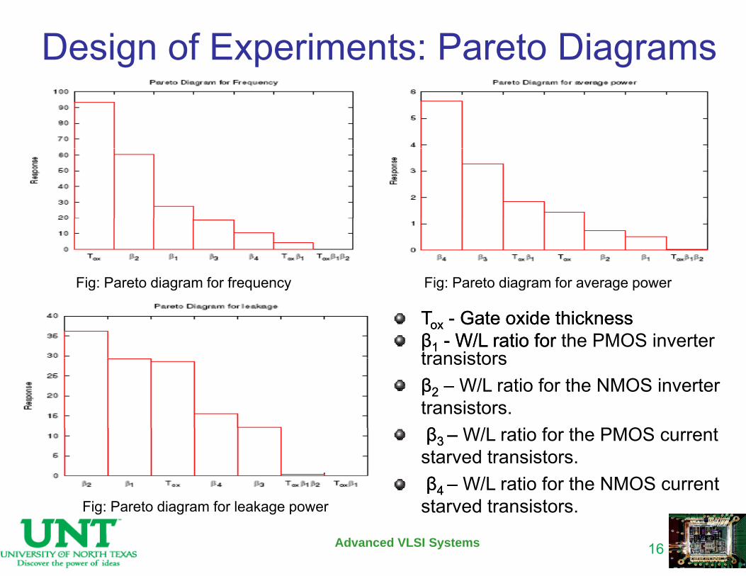
Design of Experiments: Pareto Diagrams
Fig: Pareto diagram for frequency Fig: Pareto diagram for average powerg g q y g g g p
TToxox -- Gate oxide thicknessGate oxide thicknessββ11 -- W/L ratio for W/L ratio for the PMOS inverter transistorstransistorsββ22 – W/L ratio for the NMOS inverter transistors.ββ W/L ti f th PMOS tββ3 3 –– W/L ratio for the PMOS current starved transistors.ββ4 4 –– W/L ratio for the NMOS current
Fig: Pareto diagram for leakage power starved transistors.
16Advanced VLSI Systems

Design of Experiments: Prediction Equations and OptimizationEquations and Optimization
• Prediction equations for the outputs considered:q p– F^ = 786.43 - 93.36Tox + 60.3 β2– P^ = 35.05 + 5.7 β4 + 3.3 β3– PL^ = 376.35 – 28.58 To + 29.32 β1+ 36.17 β2PL 376.35 28.58 Tox 29.32 β1 36.17 β2
• Optimization of frequency of operation:To maximize the frequency of oscillation T must be 1 while β must be– To maximize the frequency of oscillation, Tox must be -1 while β2 must be+1
• Optimization of average power:• Optimization of average power:– β4 and β3 must be -1, as average power has to be minimized
Optimization of leakage power:• Optimization of leakage power:– Tox and β1 must be -1 and β2 must be +1
17Advanced VLSI Systems

Frequency Divider• In any flip-flop, when a continuous train of pulse waveforms at fixed
frequency is fed to it as an input signal, an output signal of approximatelyhalf the frequency of the input signal can be obtainedhalf the frequency of the input signal can be obtained
• Design and Working– JK flip-flop: realized using two 3-input and two 2-input NAND gates– Principle: count two pulses and then reset– Principle: count two pulses and then reset
Fig: Circuit diagram of a J-K flip-flop
18Advanced VLSI Systems

Analog Design and Simulation Results of a Frequency Dividerof a Frequency Divider
Fig: Transistor level circuit diagram of a frequency divider
Fig: Simulation results of the VCO and frequency divider for an input voltage of 0.7Vfrequency divider p g
19Advanced VLSI Systems
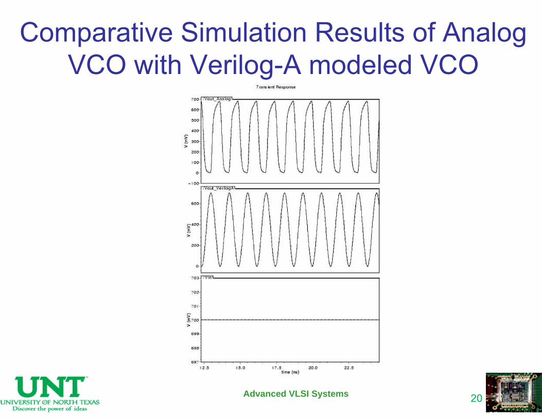
Comparative Simulation Results of Analog VCO ith V il A d l d VCOVCO with Verilog-A modeled VCO
20Advanced VLSI Systems

Phase Frequency Detector• Compares the phase of the local oscillator to that of the reference signal
Directs the charge p mp to s ppl charge amo nts in proportion to the• Directs the charge pump to supply charge amounts in proportion to thephase error detected
Detects the phase or frequency differences and produces the resultant error• Detects the phase or frequency differences and produces the resultant errorvoltage (output is proportional to the difference in phase or frequency)
• Types of phase detectors:• Types of phase detectors:– XOR gate– Four-quadrant multiplier, also known as a mixer
B b h h d t t– Bang-bang charge pump phase detector– Proportional phase detector
• A PFD is realized using two D flip-flops and one 2-input NAND gate
21Advanced VLSI Systems
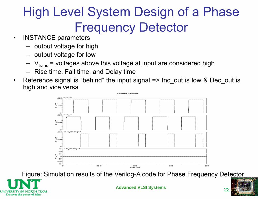
High Level System Design of a Phase Frequency DetectorFrequency Detector
• INSTANCE parameters– output voltage for high– output voltage for low– Vtrans = voltages above this voltage at input are considered high– Rise time, Fall time, and Delay time
• Reference signal is “behind” the input signal => Inc_out is low & Dec_out ishigh and vice versa
Fi Si l ti lt f th V il A d f Ph F D t tPh F D t tFigure: Simulation results of the Verilog-A code for Phase Frequency DetectorPhase Frequency Detector
22Advanced VLSI Systems

Simulation Results of the Analog Design for a Phase Frequency DetectorDesign for a Phase Frequency Detector
Fig: Circuit diagram of a D flip-flop
Fig: Circuit diagram of a PFD
23Advanced VLSI Systems

Simulation Results of the Analog Design for a Phase Frequency DetectorDesign for a Phase Frequency Detector
Fig: Simulation results of the PFD
24Advanced VLSI Systems

Comparative Simulation Results of Analog PFD with Verilog-A modeled PFDPFD with Verilog A modeled PFD
Fig: Comparative view of the simulation results of the Dec_out signal for a PFD for the analog and Verilog-A system design approaches
Fig: Comparative view of the simulation results of the Inc_out signal for a PFD for the analog and Verilog-A system design approachesy g pp y g pp
25Advanced VLSI Systems

Charge PumpCharge Pump• Stabilizes spurious fluctuation of currents and switching time, to minimize the
spurs in the VCO inputspurs in the VCO input
• Manipulates the amount of charge on the filter's capacitors depending uponthe signals from the UP and DOWN outputs of the PFD
• Principle: two current sources and two switches controlled by the PFD outputs
& O• UP is High & DOWN is Low => Vout increases => sources current on to thecapacitor
• UP is Low & DOWN is High =>V decreases => sinks current on the• UP is Low & DOWN is High =>Vout decreases => sinks current on thecapacitor
• UP is Low & DOWN is Low => Vout is constant and Iout is zeroout out
• Power analysis proves that the designed charge pump acts as a power source
26Advanced VLSI Systems

Analog Design and Simulation Results f th Ch Pof the Charge Pump
Fig: Transistor level circuit diagram of the charge pump
Fig: Simulation results of the charge pump at an input voltage of 0 7Vpump voltage of 0.7V
27Advanced VLSI Systems

Power Analysis on a Charge Pump• Average power and gate leakage power are calculated• Gate leakage is a major component of leakage
Scaling in gate o ide thickness res lts in an alarming increase in gate• Scaling in gate oxide thickness results in an alarming increase in gateleakage current due to tunneling through the thin gate oxide.
• Average power calculated for the whole device = 104.732 μWTable: Power analysis on a 45 nm charge pump
28Advanced VLSI Systems

Transistor Wise Power Analysis According to Region of Operation on a Charge Pumpto Region of Operation on a Charge Pump
• Regions of operation– Triode– Saturation
S b th h ld
Table: Power Analysis for transistor M0 according to each region of operation in a charge pump
– Sub-threshold• Sub-threshold leakage power is a
vital component in the total powerconsumption as scaling of deviceco su p o as sca g o de cedimensions and threshold voltageresults in increased sub-thresholdleakage
• Sub threshold power was• Sub-threshold power wasnegligible when compared to thetotal power
• Total power consumed (transistori l l ti ) i 91 74 Wwise calculations) is 91.74 μW
29Advanced VLSI Systems

Low Pass Filter
• Low pass RC filter passes frequency signals within the range of the VCOLow pass RC filter passes frequency signals within the range of the VCO
• Principle: Cutoff frequency of the filter is approximately equal to themaximum frequency of the VCO => the filter will reject signals atf i b th i f f th VCOfrequencies above the maximum frequency of the VCO
• RC filter acts as a AC voltage divider circuit that discriminates against highfrequencies as the capacitive reactance decreases with frequencyfrequencies, as the capacitive reactance decreases with frequency
• Low-pass filter smoothes out the abrupt control inputs from the chargepumpp p
30Advanced VLSI Systems

High Level System Design of a Low P FiltPass Filter
• INSTANCE parameters– bandwidth of the filterbandwidth of the filter
• fcutoff = 1/ (2π*R*C); where R=1K and fcutoff=788MHz
Figure: Simulation results of the Verilog-A code for a low pass filter for an input voltage of 0.7Va low pass filter for an input voltage of 0.7V
Figure: Simulation results of the Verilog-A code for a low pass filter on a dB scale.a low pass filter on a dB scale.
31Advanced VLSI Systems

Analog Design and Simulation Results of the Low Pass Filterof the Low Pass Filter
Figure: Circuit diagram of a low pass RC filter
Figure: Simulation results for the low pass RC filterlow pass RC filter Figure: Simulation results for the low pass RC filter the low pass RC filter Figure: Simulation results for the low pass RC filterlow pass RC filteron a dB scale.on a dB scale.
32Advanced VLSI Systems

Comparative Simulation Results of Analog Low Pass Filter with Verilog-A modeled LowLow Pass Filter with Verilog A modeled Low
Pass Filter
Fig: Comparative view of the simulation results of the low pass filter for the analog and Verilog-A system design approaches
Fig: Comparative view of the simulation results of the low pass filter for the analog and Verilog-A system design approaches on a dB scaledesign approaches design approaches on a dB scale
33Advanced VLSI Systems

Mixed Signal AnalysisAnalog circuits• Analog circuits– Signals are continuously varying voltages, currents or frequencies =>
provide accuracyVoltage scaling and library design are the two problems related to the– Voltage scaling and library design are the two problems related to theanalog circuits
• Digital circuits– Signals are two-level discrete voltages that are either low or high =>Signals are two-level discrete voltages that are either low or high =>
provide speed– Digital library can be easily built as any digital circuit would be a
combination of different logic functions like NAND, NOR and data storagecombination of different logic functions like NAND, NOR and data storageelements like flip-flops
• Issues with Analog CircuitsDecrease in supply voltage leads to lower performance– Decrease in supply voltage leads to lower performance
– Gate leakage• Mixed signal circuits
High accuracy and speed along with low cost and low power consumption– High accuracy and speed along with low cost and low power consumption– provide improved system reliability and flexibility– System performance is usually limited by the a2d or d2a interfaces as the
d f th d t i h t b t dspeed of the data conversion has to be accounted
34Advanced VLSI Systems

Mixed Signal Analysis on VCO and F Di idFrequency Divider
• VCO – Analog design => Transistor level• Frequency divider – Digital design => Behavioral Verilog code• Frequency of operation:
– For VCO, fVCO = 717.96 MHz– For analog frequency divider, fa = 358.98 MHz– For digital frequency divider, fd = 394.03 MHz
• Difference in frequency is due to:R l iti l di– Regular capacitive loading
– Gate tunneling or leakage• The difference in frequencies can be removed by adding a capacitor CLOAD of
2 49 fF of which 2 fF is due to gate tunneling and 0 49 fF is due to capacitive2.49 fF of which 2 fF is due to gate tunneling and 0.49 fF is due to capacitiveloading
• Optimized Values of the Output Metric:– F^ = 786 43 MHzF 786.43 MHz– P^ = 61.354 μW– PL^ = 647.38 pW
35Advanced VLSI Systems

Mixed Signal Analysis: Experimental Results
Figure: Block diagram of the VCO along with an analog frequency divider and a digital frequency divider
Figure: Output waveforms of the VCO digital frequency divider and analog frequency dividerFigure: Output waveforms of the VCO, digital frequency divider and analog frequency divider
36Advanced VLSI Systems
Top Related