


Languages
Pages
Legal


ECE 3040 - Dr. Alan DoolittleGeorgia Tech
Lecture 15
P-N Junction Diodes: Part 5
Large signal (complete model) and small signal (limited use) models of a Diode
Reading:
Jaeger 3.4-3.14, 13.4, Notes
ECE 3040 - Dr. Alan DoolittleGeorgia Tech
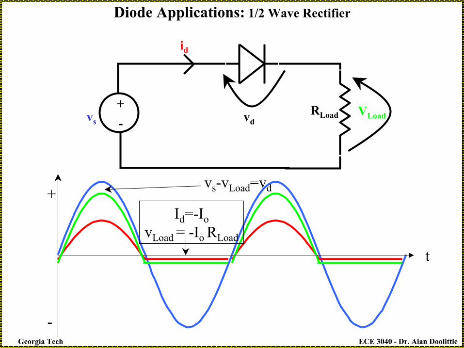
Diode Applications: 1/2 Wave Rectifier
RLoadvd
id
vs
+-
t
VLoad
vs-vLoad=vd+
-
Id=-IovLoad = -Io RLoad
ECE 3040 - Dr. Alan DoolittleGeorgia Tech
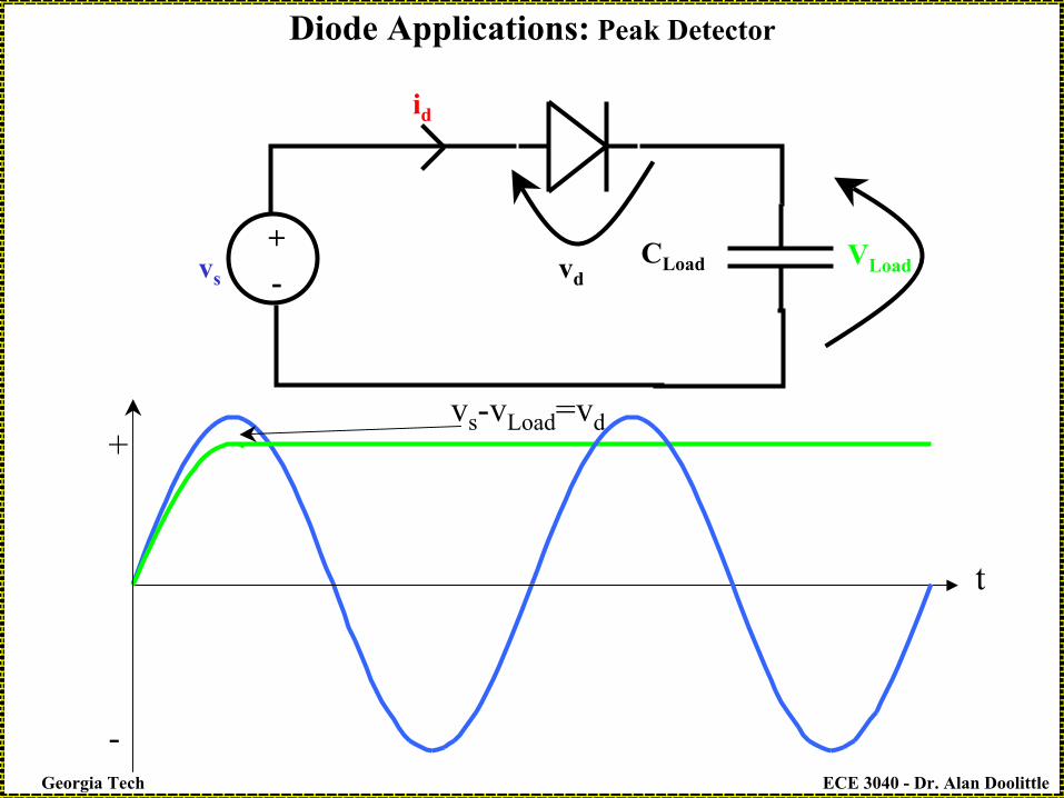
Diode Applications: Peak Detector
CLoadvd
id
vs
+-
t
VLoad
vs-vLoad=vd+
-

ECE 3040 - Dr. Alan DoolittleGeorgia Tech
Diode Applications: 1/2 Wave Rectifier with an RC Load
RLoad
id
vs
+-
t
VLoad
+
-
CLoad

ECE 3040 - Dr. Alan DoolittleGeorgia Tech
Diode Applications: LED or a Laser Diode
R=1000 ohms
V=9V VA
I V1=IR Light Emission under forward Bias
Diode made from a direct bandgap semiconductor. Note: These devices may not be a simple p-n type diode, but behave electrically identical to a p-n junction diode.
Majority Carriers that are injected to the oppposite side of the diode under forward bias become minority carriers and recombine. In a direct bandgap material, this recombination can result in the creation of photons. In a real device, special areas are used to trap electrons and holes to increase the rate at which they recombine. These areas are called quantum wells.
LightFN
FP
-qVA
Quantum well made from smaller bandgap material
Electron Current
Hole Current
P-type Al0.5Ga0.5As
N-type Al0.5Ga0.5As
GaAs
ECE 3040 - Dr. Alan DoolittleGeorgia Tech
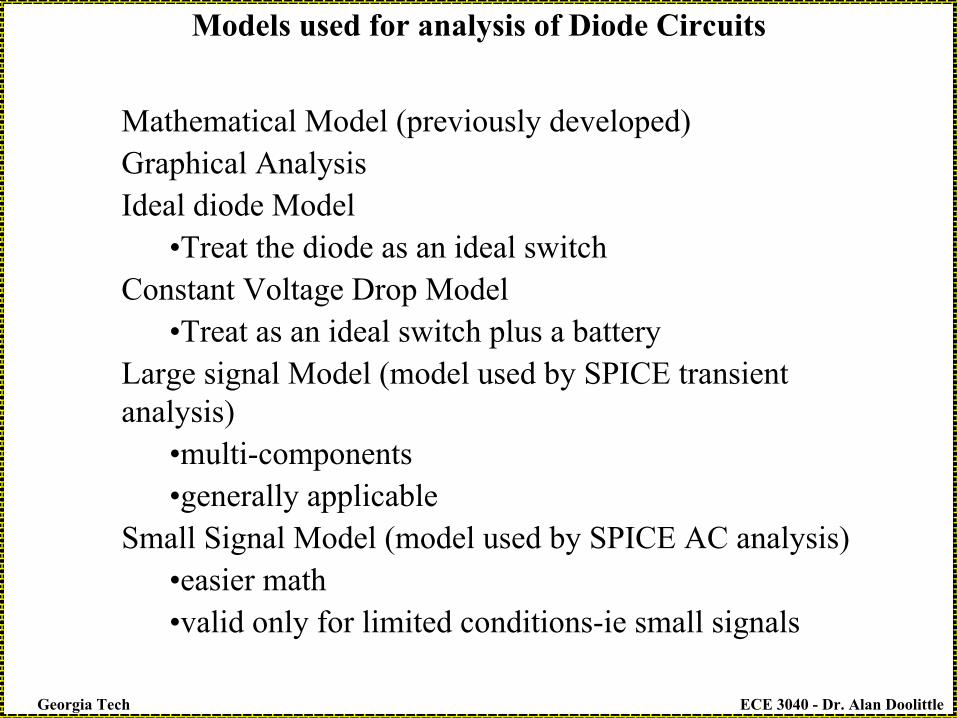
Models used for analysis of Diode Circuits
Mathematical Model (previously developed)Graphical AnalysisIdeal diode Model
•Treat the diode as an ideal switchConstant Voltage Drop Model
•Treat as an ideal switch plus a batteryLarge signal Model (model used by SPICE transient analysis)
•multi-components•generally applicable
Small Signal Model (model used by SPICE AC analysis)•easier math•valid only for limited conditions-ie small signals

ECE 3040 - Dr. Alan DoolittleGeorgia Tech
Diode Circuits: Graphical Solution
R=1000 ohms
V=9V VA
I V1=IR
Load Line
I=0 -> VA=9V
VA=0V -> I=9V/1000 ohms
Intersection of the two curves gives the DC operational voltage and currents
To solve the problem graphically, we need to find the IV curve for the resistor:
VD
ID

ECE 3040 - Dr. Alan DoolittleGeorgia Tech
Diode Circuits: Other Models
Besides the direct mathematical solution and the graphical solution, we can use 2 other models to approximate circuit solutions:
1.) Ideal Diode Model:
a) The voltage across the diode is zero for forward bias.
b) The slope of the current voltage curve is infinite for forward bias.
c) The current across the diode is zero for reverse bias.
V
ICircuit Symbol

ECE 3040 - Dr. Alan DoolittleGeorgia Tech
Diode Circuits: Other Models
2.) Constant Voltage Drop (CVD) Model:
a) The voltage across the diode is a non-zero value for forward bias. Normally this is taken as 0.6 or 0.7 volts.
b) The slope of the current voltage curve is infinite for forward bias.
c) The current across the diode is zero for reverse bias.
V
I
0.6V+
-Von

ECE 3040 - Dr. Alan DoolittleGeorgia Tech
Concept of the Small- Signal Model•Superposition principle allows us to separate DC and AC analysis of circuits containing active devices (like diodes, transistors, amplifiers etc...).•We assume the AC signals are small enough so that the circuit behaves linearly and can be analyzed by replacing “non-linear” components by “Linear Elements” such as resistors etc...•DC analysis is first performed to determine the bias point whichwill determine some of the parameters used in the “AC-small signal analysis”.•Consider a two terminal device (like a pn diode) at a given DC operating point (or “Q- point”).Let: VD = DC voltage applied to the diode
ID = DC current produced by the diodeTotal current or voltage = DC part + AC part:
vD = VD + vd iD = ID + idNote: (1) all caps = DC; (2) all lower case = AC; (3) lower casesymbol with upper case subscript = total voltage or current

ECE 3040 - Dr. Alan DoolittleGeorgia Tech
iD=ID+id
vD=VD+vd
VD
ID
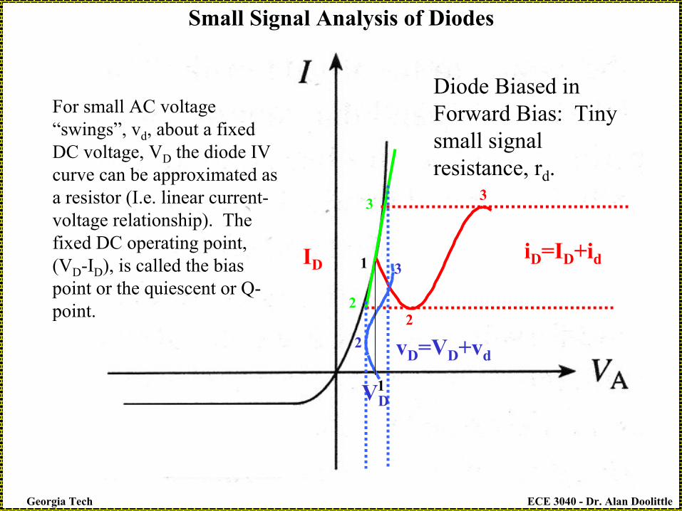
For small AC voltage “swings”, vd, about a fixed DC voltage, VD the diode IV curve can be approximated as a resistor (I.e. linear current-voltage relationship). The fixed DC operating point, (VD-ID), is called the bias point or the quiescent or Q-point.
Small Signal Analysis of Diodes
Diode Biased in Forward Bias: Tiny small signal resistance, rd.
1
1
2
22
3
ECE 3040 - Dr. Alan DoolittleGeorgia Tech
iD=ID+id
vD=VD+vd
VD
ID
For small AC voltage “swings”, vd, about a fixed DC voltage, VD the diode IV curve can be approximated as a resistor (I.e. linear current-voltage relationship). The fixed DC operating point, (VD-ID), is called the bias point or the quiescent or Q-point.
Small Signal Analysis of Diodes
Diode Biased in Forward Bias: Tiny small signal resistance, rd.
1
1
2
22
3
3
3

ECE 3040 - Dr. Alan DoolittleGeorgia Tech
iD=ID+id
vD=VD+vd
VD
ID
For small AC voltage “swings”, vd, about a fixed DC voltage, VD the diode IV curve can be approximated as a resistor (I.e. linear current-voltage relationship). The fixed DC operating point, (VD-ID), is called the bias point or the quiescent or Q-point.
Small Signal Analysis of Diodes
Diode Biased in Forward Bias: Tiny “small signal” resistance, rd.
1
1
2
22
3
3
3

ECE 3040 - Dr. Alan DoolittleGeorgia Tech
Small vs Large Signal Concept For Diodes
iD=ID+id
vD=VD+vd
0.585
0.59
0.595
0.6
0.605
0.61
0.615
0 10 20 30 40 50 60 70
Time
Volta
ge
0.0064
0.0084
0.0104
0.0124
0.0144
0.0164
0.0184
Cur
rent
Voltage 0.6V+0.025sin(wt) I=f(V)
Both Voltage and Current are (approximately) a sine wave.Some distortion is observed because in this example we have exceeded the mathematical limits valid for small signal analysis (0.025 is not << kT/q). In most cases, this is tolerable.
Consider the small signal case where
(t)v1(t)ibut(t)v1(t)i
1)-12(e-1e(t)i
then,t)0.025sin(w0.6(t)v
Dd
Ddd
d
(t)/0.0259vD
D
D
rr≠≈⇒
=
+=

ECE 3040 - Dr. Alan DoolittleGeorgia Tech
-0.8
-0.6
-0.4
-0.2
0
0.2
0.4
0.6
0.8
0 10 20 30 40 50 60 70
Time
Volta
ge
-0.01
-0.008
-0.006
-0.004
-0.002
0
0.002
0.004
0.006
0.008
0.01
Cur
rent
0.6sin(wt) I=f(V)
iD=ID+id
vD=VD+vd
2
3 3
Small vs Large Signal Concept For Diodes
Voltage is a sine wave but the current is “distorted”
Consider the Large Signal case where
(t)v1(t)i
1)-12(e-1e(t)i
then,0.6sin(wt)(t)v
Dd
D
(t)/0.0259vD
D
D
r≠⇒
=
=

ECE 3040 - Dr. Alan DoolittleGeorgia Tech
The transition from valid small signal limits to Large Signal conditions is a matter of what is acceptable for your requirements
0.585
0.59
0.595
0.6
0.605
0.61
0.615
0 10 20 30 40 50 60 70
Time
Volta
ge
0.0064
0.0084
0.0104
0.0124
0.0144
0.0164
0.0184
Curr
ent
Voltage 0.6V+0.025sin(wt) I=f(V) 0
0.02
0.04
0.06
0.08
0.1
0.12
0 10 20 30 40 50 60 70
Frequency
Mag
nitu
de o
f Sig
nal
0.5985
0.599
0.5995
0.6
0.6005
0.601
0.6015
0 10 20 30 40 50 60 70
Time
Volta
ge
0.0108
0.011
0.0112
0.0114
0.0116
0.0118
0.012
0.0122
Curr
ent
Voltage 0.6V+0.025sin(wt) I=f(V) 0
0.001
0.002
0.003
0.004
0.005
0.006
0.007
0.008
0.009
0.01
0 10 20 30 40 50 60 70
Frequency
Mag
nitu
de o
f Sig
nal
0.4
0.45
0.5
0.55
0.6
0.65
0.7
0.75
0 10 20 30 40 50 60 70
Time
Volta
ge
-0.6
-0.4
-0.2
0
0.2
0.4
0.6
Curr
ent
Voltage 0.6V+0.025sin(wt) I=f(V) 0
0.5
1
1.5
2
2.5
3
3.5
4
4.5
5
0 10 20 30 40 50 60 70
Frequency
Mag
nitu
de o
f Sig
nal
t)0.001sin(w0.6(t)vD +=1)-12(e-1e(t)i (t)/0.0259v
DD=
)0.01sin(wt0.6(t)vD +=
0.1sin(wt)0.6(t)vD +=
FFTMajor
distortion
FFTSlight
Distortion
FFT“No”
Distortion

ECE 3040 - Dr. Alan DoolittleGeorgia Tech
Small Signal Analysis of Diodes
T
SDd
T
SSV
V
S
T
VV
S
Vv
Td
Vv
VV
T
SpoQ
Vv
T
S
poQD
Vv
S
poQorQuiscientorPoBiasD
Dd
ddd
d
VII
g
VIIeI
VeI
andeVvsignalssmallgAssu
eeVI
eVI
v
eI
vig
grdiodetheofceresissignalsmallr
diodetheofceconducsignalsmallg
TD
TD
Td
Td
TD
TD
TD
+=
+−==
→⟨⟨
==
∂
−∂
=
∂∂
=
=≡
≡
−
−
−
1,,min
1
1,tan
tan
int
int
int""""int

ECE 3040 - Dr. Alan DoolittleGeorgia Tech
Small Signal Analysis of Diodes
BiasverseinV
IIg
BiasForwardinVI
g
GeneralinV
IIg
vgIi
T
SSd
T
Dd
T
SDd
ddDD
Re0≈+−
≈
≈
+=
+=q
kTVwhereeI TV
V
oT
A
=
−= 1 ID
qkTVwhereeI T
VV
oT
A
=≈→>> I 0V DA
0 0VA →→<< TA
VV
e

ECE 3040 - Dr. Alan DoolittleGeorgia Tech
iD=ID+id
vD=VD+vd
VD
Diode Biased in Reverse Bias: Huge “small signal” resistance, rd=1/gd
Small Signal Analysis of Diodes
ECE 3040 - Dr. Alan DoolittleGeorgia Tech
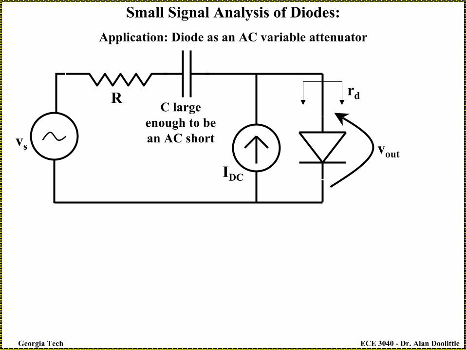
Small Signal Analysis of Diodes:Application: Diode as an AC variable attenuator
R
vs vout
IDC
C large enough to be an AC short
rd

ECE 3040 - Dr. Alan DoolittleGeorgia Tech
R
vout
rd
1.) Determine DC operating point and calculate small signal parameters, rd and others to come in later lectures)
2.) Convert to the AC only model.•DC Voltage sources are shorts•DC Current sources are open circuits•Large capacitors are short circuits•Large inductors are open circuits
Steps to Analyze a Diode Circuit
Small Signal Analysis of Diodes:Conversion to AC equivalent circuit
R
vs vout
ID
C
C large enough to be an AC
short
rd

ECE 3040 - Dr. Alan DoolittleGeorgia Tech
( )
( )RIIvv
etemperaturroomator
VRII
v
rR
vv
Rrr
vv
SDCinout
T
SDCin
d
inout
d
dinout
++≈
++
=+
=
+=
4011
1
1
1
1
R
vout
rd
Small Signal Analysis of Diodes:Application: Diode as an AC variable attenuator

ECE 3040 - Dr. Alan DoolittleGeorgia Tech
RSeries
iD=IS(exp(v’D/(ηVT)) - 1) where η accounts for previously neglected recombination-
generation in the depletion region
iD=IS(exp[(vD- iDRSeries )/(ηVT)] - 1) accounts for the series resistance drop in the quasi-
neutral regions.
CJunction
CDiffusion
voltageinchangeafromresultingechinChangedvdQC
D
arg' ==
v’D
vD
Completing the Large signal model of a diode
p-region n-region
Depletion-region
pno
npo
x=0 x=0
+++ +
++ +
+----
----
nnoppo
Actual voltage drop across the diode including resistive losses from quasi-neutral regions.
----
----
++++++++

ECE 3040 - Dr. Alan DoolittleGeorgia Tech
( ) ( )
( ) ( )
( ) ( )bi
A
JoJ
biDA
DAoSVjunctionJo
AbiDA
DAoSjunction
AbiDA
DAoSnp
osjunction
VV
CCand
VNNNNqK
ACC
ThusVVNN
NNqKAC
VVNN
NNq
KxxW
butW
AKC
A
−
=+
==
−+=
−+
=+=
=
=
1
12
,
12
2
...
0ε
ε
ε
ε
For an abrupt diode (uniform doping on both sides of the junction):
Completing the Large signal model of a diode
Junction capacitance is due to majority carrier charges displaced by the depletion width (I.e. similar to a parallel plate capacitor).
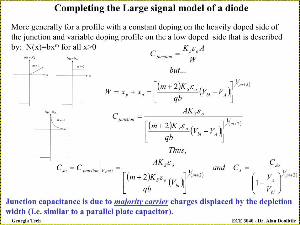
ECE 3040 - Dr. Alan DoolittleGeorgia Tech
( ) ( )( )
( ) ( )( )
( ) ( )( ) ( )2
12
10
21
21
12
,
2
2
...
++=
+
+
−
=
+==
−
+=
−
+=+=
=
m
bi
A
JoJ
m
bioS
oSVjunctionJo
m
AbioS
oSjunction
m
AbioS
np
osjunction
VV
CCand
Vqb
Km
AKCC
Thus
VVqb
Km
AKC
VVqb
KmxxW
butW
AKC
A
ε
ε
ε
ε
ε
ε
More generally for a profile with a constant doping on the heavily doped side of the junction and variable doping profile on the a low doped side that is described by: N(x)=bxm for all x>0
Junction capacitance is due to majority carrier charges displaced by the depletion width (I.e. similar to a parallel plate capacitor).
Completing the Large signal model of a diode

ECE 3040 - Dr. Alan DoolittleGeorgia Tech
[ ]
[ ]
[ ]dt
dvqALnLp
I
eI
VdtdQ
dtdv
qALnLpeVdt
dQ
qALnLpe
dxeenqAdxeepqAQ
dvdt
dtdQ
dvdQ
C
Dnpopno
S
Vv
S
T
D
Dnpopno
Vv
T
D
npopnoV
v
Lx
Vv
poL
xV
v
noD
D
D
D
DDiffusion
TD
TD
TD
nTD
pTD
'
'
00
'
'
111
1
1
11
'
'
'
''
+
+−
=
+
=
+
−=
−+
−=
=
=
∫∫∞ −∞ −
Completing the Large signal model of a diode
Diffusion capacitance due to “excess injected” minority carrier charge at the depletion region edges. Since this charge results from minority carriers, this capacitance is negligible at zero or reverse biases.

ECE 3040 - Dr. Alan DoolittleGeorgia Tech
[ ][ ]
[ ]
[ ]
[ ] [ ]
[ ]
tD
DDiffusion
S
npopnottdDiffusion
ddS
npopnodDiffusion
D
D
S
npopnod
D
DDiffusion
D
S
npopnod
D
D
S
npopno
T
SDD
Dnpopno
S
SD
T
D
viCSPICEinor
timetransittheisI
qALnLpwheregC
gqcmqcmcmg
IqALnLp
gC
dvdt
dtdv
IqALnLp
gdvdt
dtdQC
dtdv
IqALnLp
gdt
dQ
dtdv
IqALnLp
VIi
dtdQ
dtdvqALnLp
IIi
VdtdQ
τ
ττ
∂∂
=
+==
=
=+
=
+==
+=
+
+=
+
+=
−
,
so) do to timefinite a requiring junction, theacross move tohave carriers y the(physicall in voltage change a to
respondcan carrier aquickly howor
sec
sec
1
23
'
'
'
'
'
'
Diffusion capacitance due to “excess injected” minority carrier charge at the depletion region edges.
Completing the Large signal model of a diode
Unit analysis
iD=ID+id
iD~ID

ECE 3040 - Dr. Alan DoolittleGeorgia Tech
Summary of the Large signal model of a diode (SPICE Model)
( ) 1) - (eIi
VRi -v
SDT
SeriesDDη=
RSeries
CJunction
tdDiffusion gC τ=
( ) ( )( )
( )( )A
m
bi
A
JoJ
m
bioS
oSVjunctionJo
Vf
VV
CCand
Vqb
Km
AKCC
A
⇒
−
=
+==
+
+=
21
210
1
2 ε
ε
1.) Mathematical model2.) SPICE Model (this page)3.) Ideal Diode Model4.) Constant Voltage Drop (CVD) Model5.) Graphical circuit model

ECE 3040 - Dr. Alan DoolittleGeorgia Tech
Addition of Capacitance Components
No significant minority carrier concentration at the depletion region edges in reverse or small-forward bias => CD<<CJ
Significant minority carrier concentration at the depletion region edges in large-forward bias => CD>>CJ

ECE 3040 - Dr. Alan DoolittleGeorgia Tech
Summary of the Small signal model of a diode
RSeries
CJunction
( )DtdDiffusion IfgC ⇒= τ
( ) ( )( )
( )( )A
m
bi
A
JoJ
m
bioS
oSVjunctionJo
Vf
VV
CCand
Vqb
Km
AKCC
A
⇒
−
=
+==
+
+=
21
210
1
2 ε
ε
T
SDdddDD V
IIgwherevgIi
+=+=
( )DIf⇒= dd 1/gr

ECE 3040 - Dr. Alan DoolittleGeorgia Tech
•Series resistance to account for finite resistance of the quasi-neutral regions and metal contact resistance's.•Diode “ideality factor”, η, to account for thermal recombination-generation in the depletion region.•Junction capacitance due to majority carrier charges displaced by the depletion width (I.e. similar to a parallel plate capacitor).•Diffusion capacitance due to “excess injected” minority carrier charge at the depletion region edges. Since this charge results from minority carriers, this capacitance is negligible at zero or reverse biases.
Things we have added to account for “Non-ideal” behavior
• Reverse “Breakdown” characteristics•“Breakdown” is a deceptive term because no damage typically occurs to the device. Often diodes are designed to operate in the breakdown mode.
Things we still need to add to account for “Non-ideal” behavior

ECE 3040 - Dr. Alan DoolittleGeorgia Tech
Breakdown Mechanisms
Avalanche Breakdown:Excess current flows due to electron-hole pair multiplication due to impact ionization. This current rapidly increases with increasing reverse bias.

ECE 3040 - Dr. Alan DoolittleGeorgia Tech
Breakdown Mechanisms
Zener Breakdown:Excess current flows due to bonding electrons “tunneling” into empty conduction band states. The “tunneling barrier” must be sufficiently thin. This current rapidly increases with increasing reverse bias.

ECE 3040 - Dr. Alan DoolittleGeorgia Tech
“Zener” Diodes
Zener diodes may actually operate based on either avalanche or zener breakdown mechanisms.
Rule of thumb: |VBR|>6EG/q is typically Avalanche Breakdown
R
V>VBR
VBR almost constant can act as a high voltage (~1V -100 V) DC reference
I
Slightly different symbol
Top Related