


Languages
Pages
Legal

Dr. R.Samuel Rajesh Babu* et al. /International Journal of Pharmacy & Technology
IJPT| Sep-2016 | Vol. 8 | Issue No.3 | 16638-16652 Page 16638
ISSN: 0975-766X
CODEN: IJPTFI
Available Online through Research Article
www.ijptonline.com COMPARATIVE ANALYSIS OF PID CONTROLLED QUASI SINGLE STAGE
INVERTER FOR RENEWABLE ENERGY SYSTEM Dr. R.Samuel Rajesh Babu*, S.Madhubala, A.V.Prituja
Sathyabama University
Email: [email protected]
Received on 06-08-2016 Accepted on 27-08-2016
Abstract
The main objective of this paper is to compare the performance of Quasi Single Stage Inverter (QSSI) for Renewable
Energy System. The QSSI system is composed of active switches it is utilized to perform voltage buck and boost
conversion without using additional passive elements, which is in favour to the system power density and efficiency.
The comparative analysis are presented and the control strategy applied in the QSSI is also developed. The
performance of QSSI with PID controller is accurate and fast response. The simulation results are verified
experimentally and the output is free from ripples and has a regulated output voltage.
Keywords: Quasi Single Stage Inverter(QSSI),PID Controller, Active switches, Sinusoidal pulse width modulation
(SPWM), Bidirectional switches, Renewable energy system.
1. Introduction
Non-renewable energy sources like fossil fuels are mostly used for obtaining power but this is becoming too
expensive or too environmentally damaging to retrieve. The next best alternative for power generation is the use of
renewable energy sources. These resources are naturally replenished on human timescale such as Solar, Wind,
Geothermal, Hydroelectric power and Ocean. The applications of these resources are mainly found in electricity
generation, power plants, hot water, motor fuels and various industries.
These energy sources have less maintenance, little or no waste products such as carbon dioxide, or other pollutants.
Thus it has less impact on the environment and brings many benefits to the economy. Solar energy is one of the most
important renewable energy source which contributes to 6000 times the energy used by all human. Solar cells which
are otherwise called as photovoltaic cell are used for the direct conversion of solar energy into electric energy. These
are constructed using semiconductor device like silicon with one or more materials in presence of sunlight exhibits
unique properties. These renewable energy resources would include wide variations and hence the proposed circuit
Dr. R.Samuel Rajesh Babu* et al. /International Journal of Pharmacy & Technology
IJPT| Sep-2016 | Vol. 8 | Issue No.3 | 16638-16652 Page 16639
will adapt to these fluctuations. In conventional unit the inverter needs both voltage buck and boost conversion, low
power density, poor stability and low efficiency. The conventional inverter introduces additional transformer and
passive components to boost its voltage, which leads to more size and expensive in cost. To overcome these problems
Quasi single stage inverter (QSSI) has been proposed to interface with Renewable energy system.
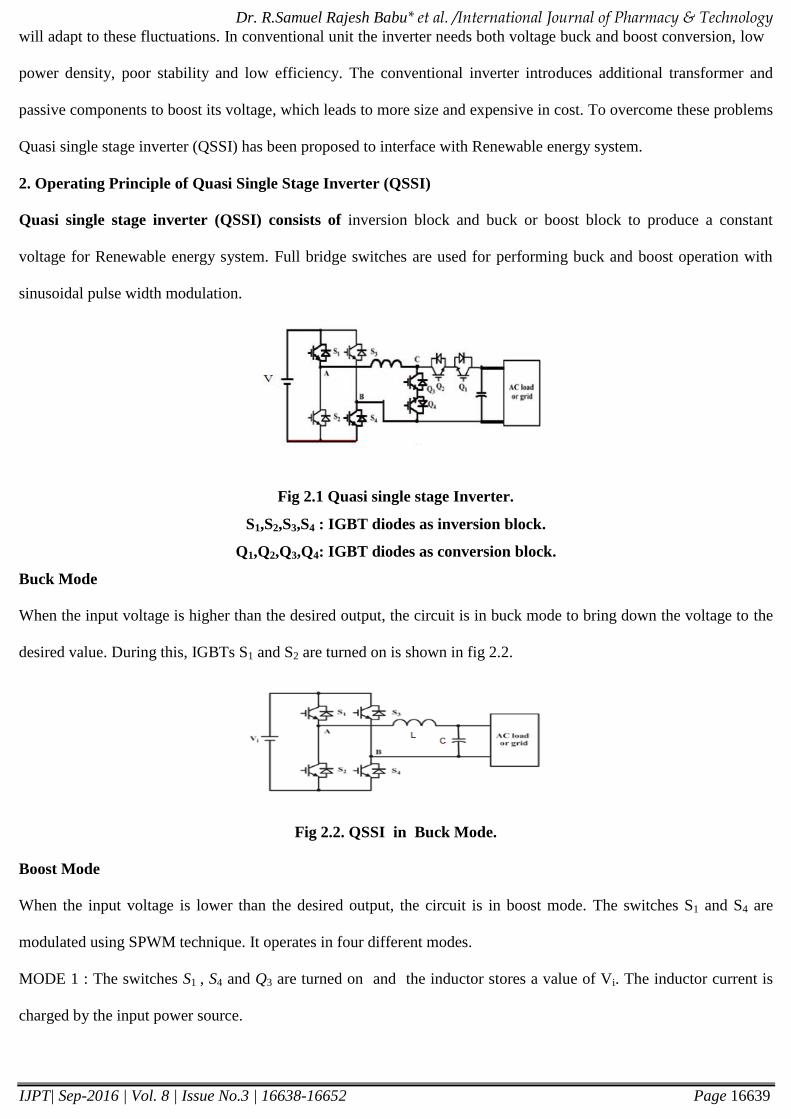
2. Operating Principle of Quasi Single Stage Inverter (QSSI)
Quasi single stage inverter (QSSI) consists of inversion block and buck or boost block to produce a constant
voltage for Renewable energy system. Full bridge switches are used for performing buck and boost operation with
sinusoidal pulse width modulation.
Fig 2.1 Quasi single stage Inverter.
S1,S2,S3,S4 : IGBT diodes as inversion block.
Q1,Q2,Q3,Q4: IGBT diodes as conversion block.
Buck Mode
When the input voltage is higher than the desired output, the circuit is in buck mode to bring down the voltage to the
desired value. During this, IGBTs S1 and S2 are turned on is shown in fig 2.2.
Fig 2.2. QSSI in Buck Mode.
Boost Mode
When the input voltage is lower than the desired output, the circuit is in boost mode. The switches S1 and S4 are
modulated using SPWM technique. It operates in four different modes.
MODE 1 : The switches S1 , S4 and Q3 are turned on and the inductor stores a value of Vi. The inductor current is
charged by the input power source.

Dr. R.Samuel Rajesh Babu* et al. /International Journal of Pharmacy & Technology
IJPT| Sep-2016 | Vol. 8 | Issue No.3 | 16638-16652 Page 16640
Fig 2.3. Mode 1 operation.
MODE 2: The switches S2, S4 and Q3 are turned on and inductor is equal to 0. The inductor current is in the
freewheeling state.
Fig 2.4 Mode 2 operation.
MODE 3: The switches S1, S4 and Q1 are turned on.The value of inductor is equal to the difference between the
input and output voltage. The inductor current increases when input is greater than the output whereas it decreases
when input is less than output voltage.
Fig 2.5 Mode 3 operation.
MODE 4: The switches S2, S4 and Q1 are turned on and the value of the inductor is equal to the negative of the
output voltage and the inductor current decreases. Any one of the three operating modes exist in one switching cycle.
Fig 2.6 Mode 4 operation.

Dr. R.Samuel Rajesh Babu* et al. /International Journal of Pharmacy & Technology
IJPT| Sep-2016 | Vol. 8 | Issue No.3 | 16638-16652 Page 16641
Derivation of QSSI Topology
A sinusoidal pulse width modulation (SPWM) strategy can be applied in the full-bridge switches, and the
fundamental voltage of the bridge output voltage VAB can be expressed as
V AB_F = M Vi sin wt (1)
Where M is the modulation ratio, the SPWM voltage is boosted by the AC-AC unit, while sharing the same inductor
with the DC-AC unit. The equivalent input voltage of the AC-AC unit can be represented as VAB_F
The output voltage is given by
Vo= VAB−F/(1-d)=MVi sin wt /(1-d) (2)
Where d is the duty ratio.
=
(3)
The output voltage can be modulated with two parameters M and d’
Buck Mode
When the input voltage is high enough to get the desired output, the QSSI operates in the buck mode to realize the
voltage step down.
Vo = M Vi sin wt (4)
Boost Mode
When the input voltage is low and not enough to get the desired output, the QSSI operates in the boost mode to
realize the voltage stepdown.
Vo =
(5)
3. Simulation Results
The Quasi single stage inverter (QSSI) performs both voltage buck and boost conversion, without introducing
additional passive elements. The QSSI is simulated in both open and closed loop using MATLAB simulink and the
results are presented. Scope is connected to display the output voltage.
The Simulated QSSI is compared with P, PI, PID Controllers and the results are shown.
The following values are found to be a near optimum for the design specifications.
PARAMETER RATING
Input Voltage 100V
R 10Ω
Dr. R.Samuel Rajesh Babu* et al. /International Journal of Pharmacy & Technology
IJPT| Sep-2016 | Vol. 8 | Issue No.3 | 16638-16652 Page 16642
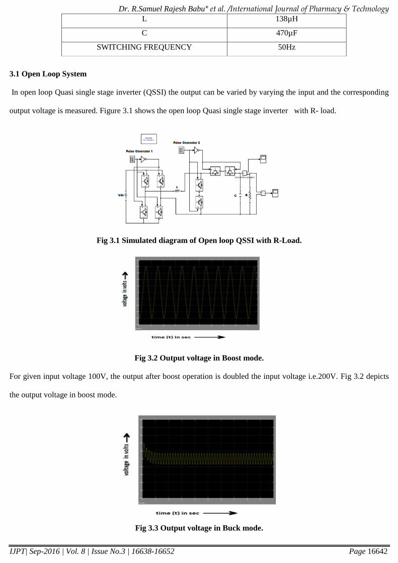
3.1 Open Loop System
In open loop Quasi single stage inverter (QSSI) the output can be varied by varying the input and the corresponding
output voltage is measured. Figure 3.1 shows the open loop Quasi single stage inverter with R- load.
Fig 3.1 Simulated diagram of Open loop QSSI with R-Load.
Fig 3.2 Output voltage in Boost mode.
For given input voltage 100V, the output after boost operation is doubled the input voltage i.e.200V. Fig 3.2 depicts
the output voltage in boost mode.
Fig 3.3 Output voltage in Buck mode.
L 138µH
C 470µF
SWITCHING FREQUENCY 50Hz
Dr. R.Samuel Rajesh Babu* et al. /International Journal of Pharmacy & Technology
IJPT| Sep-2016 | Vol. 8 | Issue No.3 | 16638-16652 Page 16643
For the given input voltage of 100V, the output after buck operation is 60V. Fig 3.3 depicts the output voltage in
buck mode. In open loop system the control action is independent of the desired output.Due to the absence of a
feedback mechanism, they are unable to remove the disturbances in the output
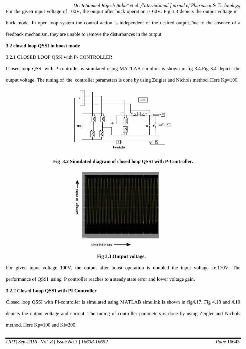
3.2 closed loop QSSI in boost mode
3.2.1 CLOSED LOOP QSSI with P- CONTROLLER
Closed loop QSSI with P-controller is simulated using MATLAB simulink is shown in fig 3.4.Fig 3.4 depicts the
output voltage. The tuning of the controller parameters is done by using Zeigler and Nichols method. Here Kp=100.
Fig 3.2 Simulated diagram of closed loop QSSI with P-Controller.
Fig 3.3 Output voltage.
For given input voltage 100V, the output after boost operation is doubled the input voltage i.e.170V. The
performance of QSSI using P controller reaches to a steady state error and lower voltage gain.
3.2.2 Closed Loop QSSI with PI Controller
Closed loop QSSI with PI-controller is simulated using MATLAB simulink is shown in fig4.17. Fig 4.18 and 4.19
depicts the output voltage and current. The tuning of controller parameters is done by using Zeigler and Nichols
method. Here Kp=100 and Ki=200.
Dr. R.Samuel Rajesh Babu* et al. /International Journal of Pharmacy & Technology
IJPT| Sep-2016 | Vol. 8 | Issue No.3 | 16638-16652 Page 16644
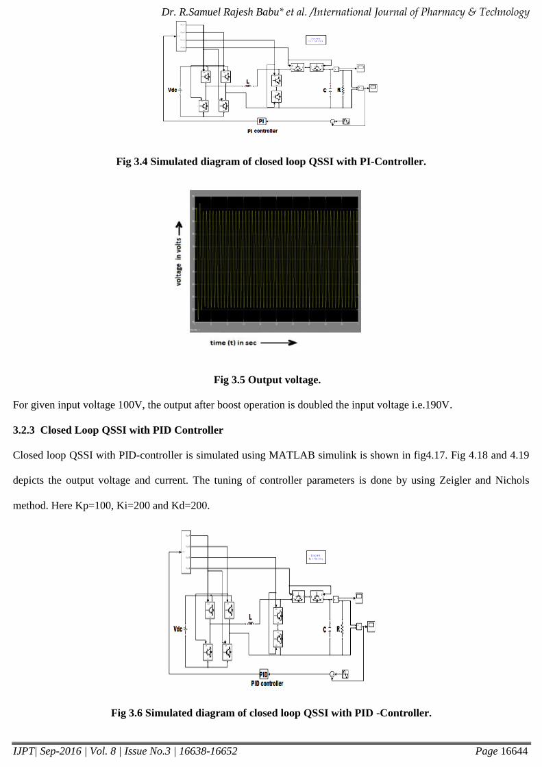
Fig 3.4 Simulated diagram of closed loop QSSI with PI-Controller.
Fig 3.5 Output voltage.
For given input voltage 100V, the output after boost operation is doubled the input voltage i.e.190V.
3.2.3 Closed Loop QSSI with PID Controller
Closed loop QSSI with PID-controller is simulated using MATLAB simulink is shown in fig4.17. Fig 4.18 and 4.19
depicts the output voltage and current. The tuning of controller parameters is done by using Zeigler and Nichols
method. Here Kp=100, Ki=200 and Kd=200.
Fig 3.6 Simulated diagram of closed loop QSSI with PID -Controller.
Dr. R.Samuel Rajesh Babu* et al. /International Journal of Pharmacy & Technology
IJPT| Sep-2016 | Vol. 8 | Issue No.3 | 16638-16652 Page 16645
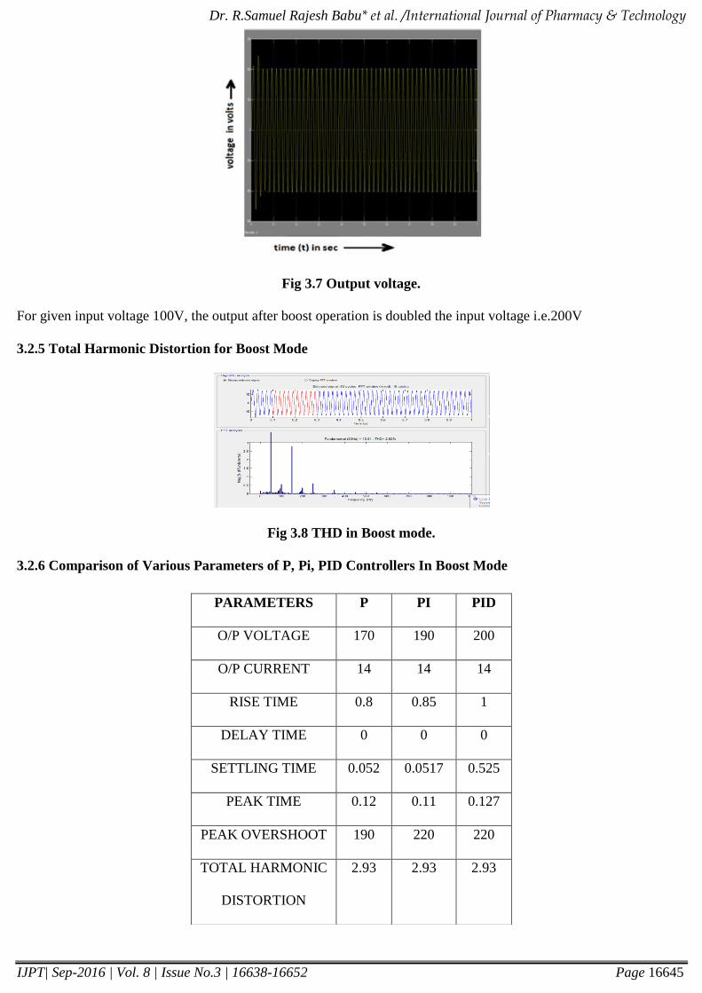
Fig 3.7 Output voltage.
For given input voltage 100V, the output after boost operation is doubled the input voltage i.e.200V
3.2.5 Total Harmonic Distortion for Boost Mode
Fig 3.8 THD in Boost mode.
3.2.6 Comparison of Various Parameters of P, Pi, PID Controllers In Boost Mode
PARAMETERS P PI PID
O/P VOLTAGE 170 190 200
O/P CURRENT 14 14 14
RISE TIME 0.8 0.85 1
DELAY TIME 0 0 0
SETTLING TIME 0.052 0.0517 0.525
PEAK TIME 0.12 0.11 0.127
PEAK OVERSHOOT 190 220 220
TOTAL HARMONIC
DISTORTION
2.93 2.93 2.93

Dr. R.Samuel Rajesh Babu* et al. /International Journal of Pharmacy & Technology
IJPT| Sep-2016 | Vol. 8 | Issue No.3 | 16638-16652 Page 16646
I/P:100V
3.3 CLOSED LOOP QSSI in BUCK MODE
3.3.1 CLOSED LOOP QSSI with P Controller
Closed loop QSSI with P-controller is simulated using MATLAB simulink is shown in fig 3.4. Fig 3.4 depicts the
output voltage. The tuning of controller parameters is done by using Zeigler and Nichols method. Here Kp=100.
Fig 3.9 Simulated diagram of closed loop QSSI with P -Controller.
Fig 3.10 Output voltage.
For given input voltage 100V, the output after buck operation is 50V
3.3.2 CLOSED LOOP QSSI with PI CONTROLLER
Closed loop QSSI with P-controller is simulated using MATLAB simulink is shown in fig 3.4. Fig 3.4 depicts the
output voltage. The tuning of controller parameters is done by using Zeigler and Nichols method.Here Kp=100 and
Ki=200.
Fig 3.11 Simulated diagram of closed loop QSSI with PI -Controller.
Dr. R.Samuel Rajesh Babu* et al. /International Journal of Pharmacy & Technology
IJPT| Sep-2016 | Vol. 8 | Issue No.3 | 16638-16652 Page 16647
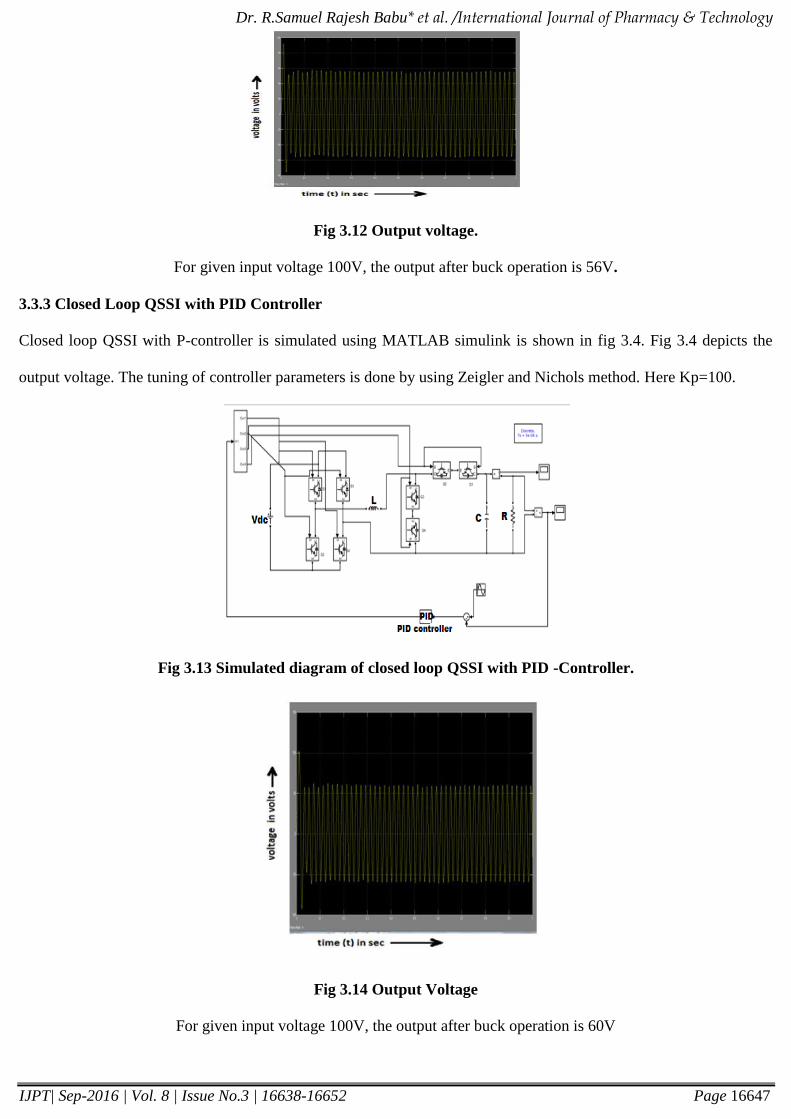
Fig 3.12 Output voltage.
For given input voltage 100V, the output after buck operation is 56V.
3.3.3 Closed Loop QSSI with PID Controller
Closed loop QSSI with P-controller is simulated using MATLAB simulink is shown in fig 3.4. Fig 3.4 depicts the
output voltage. The tuning of controller parameters is done by using Zeigler and Nichols method. Here Kp=100.
Fig 3.13 Simulated diagram of closed loop QSSI with PID -Controller.
Fig 3.14 Output Voltage
For given input voltage 100V, the output after buck operation is 60V

Dr. R.Samuel Rajesh Babu* et al. /International Journal of Pharmacy & Technology
IJPT| Sep-2016 | Vol. 8 | Issue No.3 | 16638-16652 Page 16648
3.3.4 Total Harmonic Distortion For Buck Mode
Fig 3.15 THD in Buck mode.
3.16 COMPARISON OF VARIOUS PARAMETERS OF P,PI,PID CONTROLLERS IN BUCK MODE
I/P : 100V
In closed loop system the control action is dependent on the output. The results are more accurate and reliable, even
in the presence of non-linearity. The sensitivity of the system is made small to make system more stable.
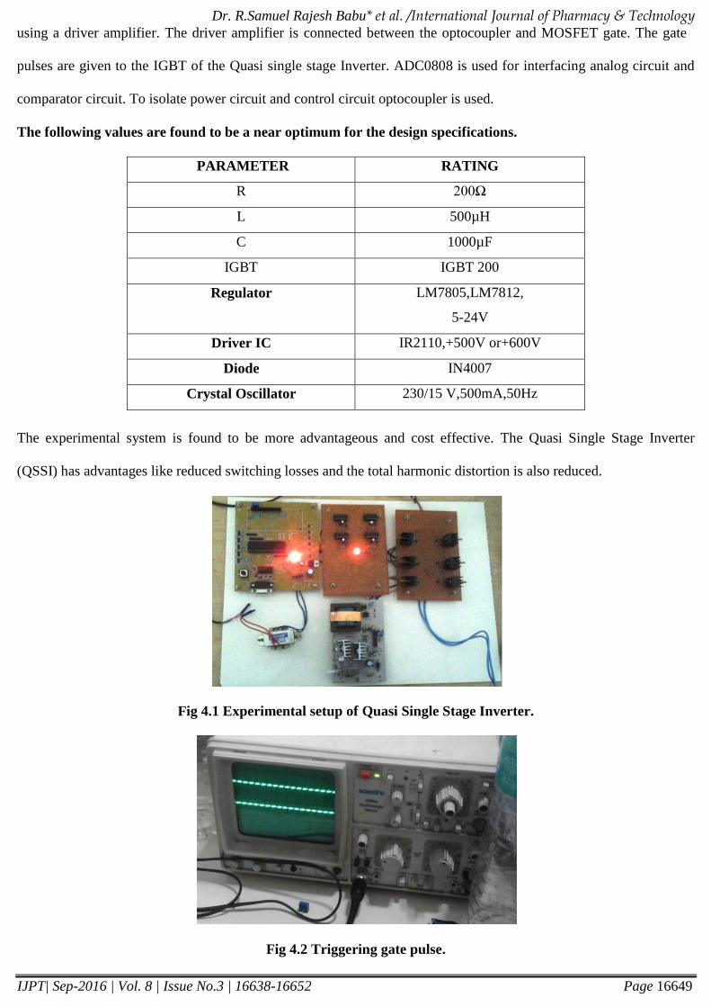
4. Experimental Results
Quasi single stage Inverter (QSSI) with full bridge switch is developed and tested in the laboratory. A PIC
Microcontroller (PIC16F877A) is mainly used to trigger the IGBT diodes at regular intervals to produce an output.
Bidirectional switches are driven by the driver circuit (IRS2110) and uses two BJT’s (n-type and p-type). Pulses
required for the MOSFET are generated by using a ATMEL microcontroller 89C2051.These pulses are amplified by
PARAMETERS P PI PID
O/P VOLTAGE 50 56 60
O/P CURRENT 4 4 4
RISE TIME 1.3 1 0.9
DELAY TIME 0 0 0
SETTLING TIME 0.335 0.31 0.32
PEAK TIME 0.087 0.087 0.08
PEAK OVERSHOOT 95 95 100
TOTAL HARMONIC
DISTORTION
2.47 2.47 2.47
Dr. R.Samuel Rajesh Babu* et al. /International Journal of Pharmacy & Technology
IJPT| Sep-2016 | Vol. 8 | Issue No.3 | 16638-16652 Page 16649
using a driver amplifier. The driver amplifier is connected between the optocoupler and MOSFET gate. The gate
pulses are given to the IGBT of the Quasi single stage Inverter. ADC0808 is used for interfacing analog circuit and
comparator circuit. To isolate power circuit and control circuit optocoupler is used.
The following values are found to be a near optimum for the design specifications.
PARAMETER RATING
R 200Ω
L 500µH
C 1000µF
IGBT IGBT 200
Regulator LM7805,LM7812,
5-24V
Driver IC IR2110,+500V or+600V
Diode IN4007
Crystal Oscillator 230/15 V,500mA,50Hz
The experimental system is found to be more advantageous and cost effective. The Quasi Single Stage Inverter
(QSSI) has advantages like reduced switching losses and the total harmonic distortion is also reduced.
Fig 4.1 Experimental setup of Quasi Single Stage Inverter.
Fig 4.2 Triggering gate pulse.
Dr. R.Samuel Rajesh Babu* et al. /International Journal of Pharmacy & Technology
IJPT| Sep-2016 | Vol. 8 | Issue No.3 | 16638-16652 Page 16650
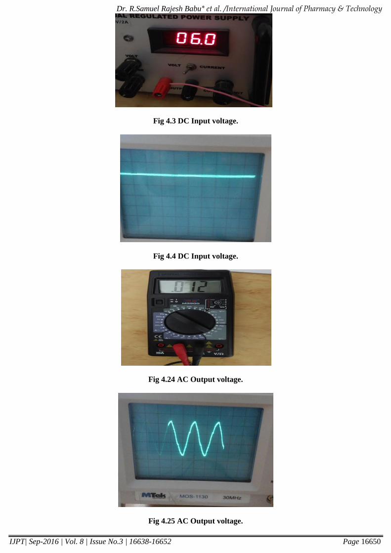
Fig 4.3 DC Input voltage.
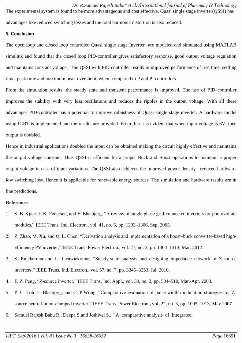
Fig 4.4 DC Input voltage.
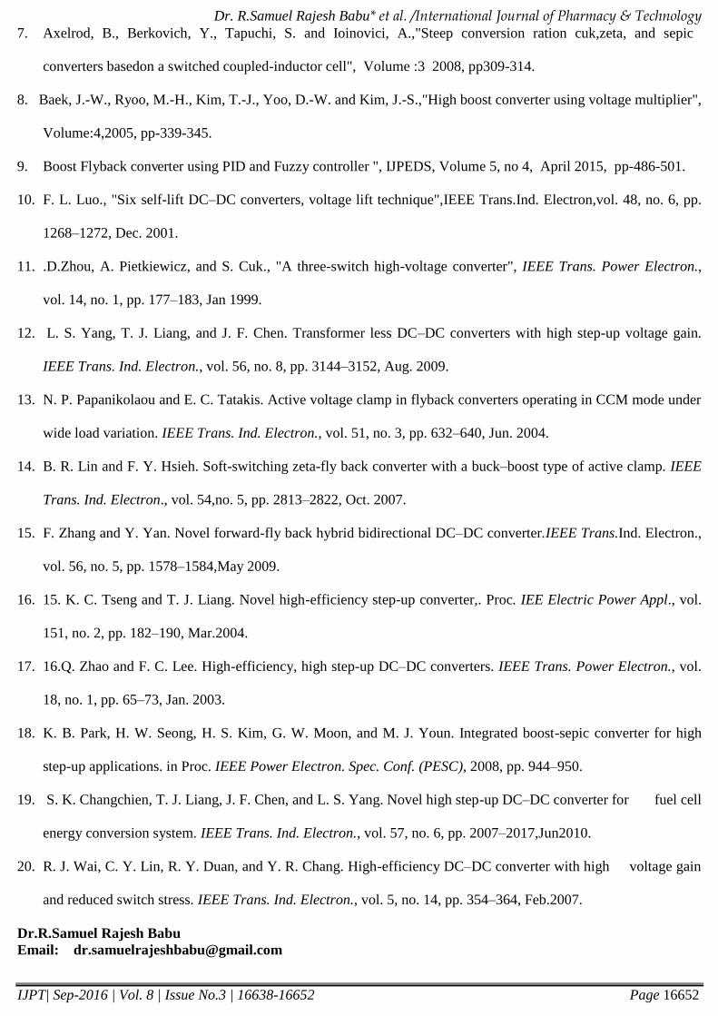
Fig 4.24 AC Output voltage.
Fig 4.25 AC Output voltage.
Dr. R.Samuel Rajesh Babu* et al. /International Journal of Pharmacy & Technology
IJPT| Sep-2016 | Vol. 8 | Issue No.3 | 16638-16652 Page 16651
The experimental system is found to be more advantageous and cost effective. Quasi single stage inverter(QSSI) has
advantages like reduced switching losses and the total harmonic distortion is also reduced.
5. Conclusion
The open loop and closed loop controlled Quasi single stage Inverter are modeled and simulated using MATLAB
simulink and found that the closed loop PID-controller gives satisfactory response, good output voltage regulation
and maintains constant voltage. The QSSI with PID controller results in improved performance of rise time, settling
time, peak time and maximum peak overshoot, when compared to P and PI controllers.
From the simulation results, the steady state and transient performance is improved. The use of PID controller
improves the stability with very less oscillations and reduces the ripples in the output voltage. With all these
advantages PID-controller has a potential to improve robustness of Quasi single stage inverter. A hardware model
using IGBT is implemented and the results are provided. From this it is evident that when input voltage is 6V, then
output is doubled.
Hence in industrial applications doubled the input can be obtained making the circuit highly effective and maintains
the output voltage constant. Thus QSSI is efficient for a proper Buck and Boost operations to maintain a proper
output voltage in case of input variations. The QSSI also achieves the improved power density , reduced hardware,
low switching loss. Hence it is applicable for renewable energy sources. The simulation and hardware results are in
line predictions.
References
1. S. B. Kjaer, J. K. Pedersen, and F. Blaabjerg, “A review of single phase grid-connected inverters for photovoltaic
modules,” IEEE Trans. Ind. Electron., vol. 41, no. 5, pp. 1292–1306, Sep. 2005.
2. Z. Zhao, M. Xu, and Q. L. Chen, “Derivation analysis and implementation of a boost–buck converter-based high-
efficiency PV inverter,” IEEE Trans. Power Electron., vol. 27, no. 3, pp. 1304–1313, Mar. 2012.
3. S. Rajakaruna and L. Jayawickrama, “Steady-state analysis and designing impedance network of Z-source
inverters,” IEEE Trans. Ind. Electron., vol. 57, no. 7, pp. 3245–3253, Jul. 2010.
4. F. Z. Peng, “Z-source inverter,” IEEE Trans. Ind. Appl., vol. 39, no. 2, pp. 504–510, Mar./Apr. 2003.
5. P. C. Loh, F. Blaabjerg, and C. P.Wong, “Comparative evaluation of pulse width modulation strategies for Z-
source neutral-point-clamped inverter,” IEEE Trans. Power Electron., vol. 22, no. 3, pp. 1005–1013, May 2007.
6. Samuel Rajesh Babu R., Deepa S.and Jothivel S., " A comparative analysis of Integrated.
Dr. R.Samuel Rajesh Babu* et al. /International Journal of Pharmacy & Technology
IJPT| Sep-2016 | Vol. 8 | Issue No.3 | 16638-16652 Page 16652
7. Axelrod, B., Berkovich, Y., Tapuchi, S. and Ioinovici, A.,"Steep conversion ration cuk,zeta, and sepic
converters basedon a switched coupled-inductor cell", Volume :3 2008, pp309-314.
8. Baek, J.-W., Ryoo, M.-H., Kim, T.-J., Yoo, D.-W. and Kim, J.-S.,"High boost converter using voltage multiplier",
Volume:4,2005, pp-339-345.
9. Boost Flyback converter using PID and Fuzzy controller ", IJPEDS, Volume 5, no 4, April 2015, pp-486-501.
10. F. L. Luo., "Six self-lift DC–DC converters, voltage lift technique",IEEE Trans.Ind. Electron,vol. 48, no. 6, pp.
1268–1272, Dec. 2001.
11. .D.Zhou, A. Pietkiewicz, and S. Cuk., "A three-switch high-voltage converter", IEEE Trans. Power Electron.,
vol. 14, no. 1, pp. 177–183, Jan 1999.
12. L. S. Yang, T. J. Liang, and J. F. Chen. Transformer less DC–DC converters with high step-up voltage gain.
IEEE Trans. Ind. Electron., vol. 56, no. 8, pp. 3144–3152, Aug. 2009.
13. N. P. Papanikolaou and E. C. Tatakis. Active voltage clamp in flyback converters operating in CCM mode under
wide load variation. IEEE Trans. Ind. Electron., vol. 51, no. 3, pp. 632–640, Jun. 2004.
14. B. R. Lin and F. Y. Hsieh. Soft-switching zeta-fly back converter with a buck–boost type of active clamp. IEEE
Trans. Ind. Electron., vol. 54,no. 5, pp. 2813–2822, Oct. 2007.
15. F. Zhang and Y. Yan. Novel forward-fly back hybrid bidirectional DC–DC converter.IEEE Trans.Ind. Electron.,
vol. 56, no. 5, pp. 1578–1584,May 2009.
16. 15. K. C. Tseng and T. J. Liang. Novel high-efficiency step-up converter,. Proc. IEE Electric Power Appl., vol.
151, no. 2, pp. 182–190, Mar.2004.
17. 16.Q. Zhao and F. C. Lee. High-efficiency, high step-up DC–DC converters. IEEE Trans. Power Electron., vol.
18, no. 1, pp. 65–73, Jan. 2003.
18. K. B. Park, H. W. Seong, H. S. Kim, G. W. Moon, and M. J. Youn. Integrated boost-sepic converter for high
step-up applications. in Proc. IEEE Power Electron. Spec. Conf. (PESC), 2008, pp. 944–950.
19. S. K. Changchien, T. J. Liang, J. F. Chen, and L. S. Yang. Novel high step-up DC–DC converter for fuel cell
energy conversion system. IEEE Trans. Ind. Electron., vol. 57, no. 6, pp. 2007–2017,Jun2010.
20. R. J. Wai, C. Y. Lin, R. Y. Duan, and Y. R. Chang. High-efficiency DC–DC converter with high voltage gain
and reduced switch stress. IEEE Trans. Ind. Electron., vol. 5, no. 14, pp. 354–364, Feb.2007.
Dr.R.Samuel Rajesh Babu
Email: [email protected]
Top Related