


Languages
Pages
Legal

irfu
saclay
Achievements & Perspectives of MIMOSA Sensors (MAPS) for Vertexing Applications
Christine Hu-Guo (IPHC)
on behalf of IPHC (Strasbourg) & IRFU (Saclay) collaboration
Outline Achieved MAPS (Monolithic Active Pixel Sensors) performances R&D for improving MAPS performances
Increase readout speed Fast readout architecture Applications and perspectives
Improve radiation tolerance Projection beyond present (2D sensors) & perspectives
Conclusion
IRFU - IPHC [email protected] 214-18/09/2009 Vertex-2009
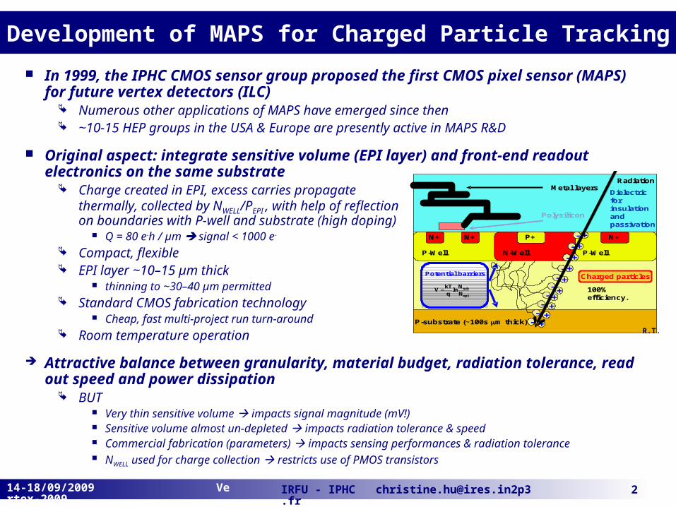
Development of MAPS for Charged Particle Tracking
In 1999, the IPHC CMOS sensor group proposed the first CMOS pixel sensor (MAPS) for future vertex detectors (ILC)
Numerous other applications of MAPS have emerged since then ~10-15 HEP groups in the USA & Europe are presently active in MAPS R&D
Original aspect: integrate sensitive volume (EPI layer) and front-end readout electronics on the same substrate
Charge created in EPI, excess carries propagate thermally, collected by NWELL/PEPI , with help of reflection on boundaries with P-well and substrate (high doping)
Q = 80 e-h / µm signal < 1000 e- Compact, flexible EPI layer ~10–15 µm thick
thinning to ~30–40 µm permitted Standard CMOS fabrication technology
Cheap, fast multi-project run turn-around Room temperature operation
Attractive balance between granularity, material budget, radiation tolerance, read out speed and power dissipation
BUT Very thin sensitive volume impacts signal magnitude (mV!) Sensitive volume almost un-depleted impacts radiation tolerance & speed Commercial fabrication (parameters) impacts sensing performances & radiation tolerance NWELL used for charge collection restricts use of PMOS transistors
IPHC-DUT [email protected] 714-18/01/2008
iPHC
Metal layers
Polysilicon
P-Well N-Well P-Well
N+ N+ P+ N+
Dielectric for insulation and passivation
Charged particles
100% efficiency.
Radiation
--
--
--
- ++
+++
++
- +- +- +
P-substrate (~100s m thick)
P-epitaxial layer(up to to 20 m thick)
Potential barriers
epi
sub
N
Nln
q
kTV
R.T.
IRFU - IPHC [email protected] 314-18/09/2009 Vertex-2009
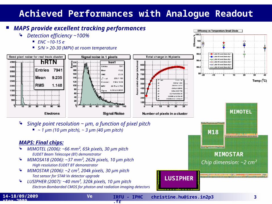
Achieved Performances with Analogue Readout MAPS provide excellent tracking performances
Detection efficiency ~100% ENC ~10-15 e- S/N > 20-30 (MPV) at room temperature
Single point resolution ~ µm, a function of pixel pitch ~ 1 µm (10 µm pitch), ~ 3 µm (40 µm pitch)
MAPS: Final chips: MIMOTEL (2006): ~66 mm², 65k pixels, 30 µm pitch
EUDET Beam Telescope (BT) demonstrator MIMOSA18 (2006): ~37 mm², 262k pixels, 10 µm pitch
High resolution EUDET BT demonstrator MIMOSTAR (2006): ~2 cm², 204k pixels, 30 µm pitch
Test sensor for STAR Vx detector upgrade LUSIPHER (2007): ~40 mm², 320k pixels, 10 µm pitch
Electron-Bombarded CMOS for photon and radiation imaging detectors
MIMOSTARChip dimension: ~2 cm²
MIMOTEL
M18
LUSIPHER
IRFU - IPHC [email protected] 414-18/09/2009 Vertex-2009
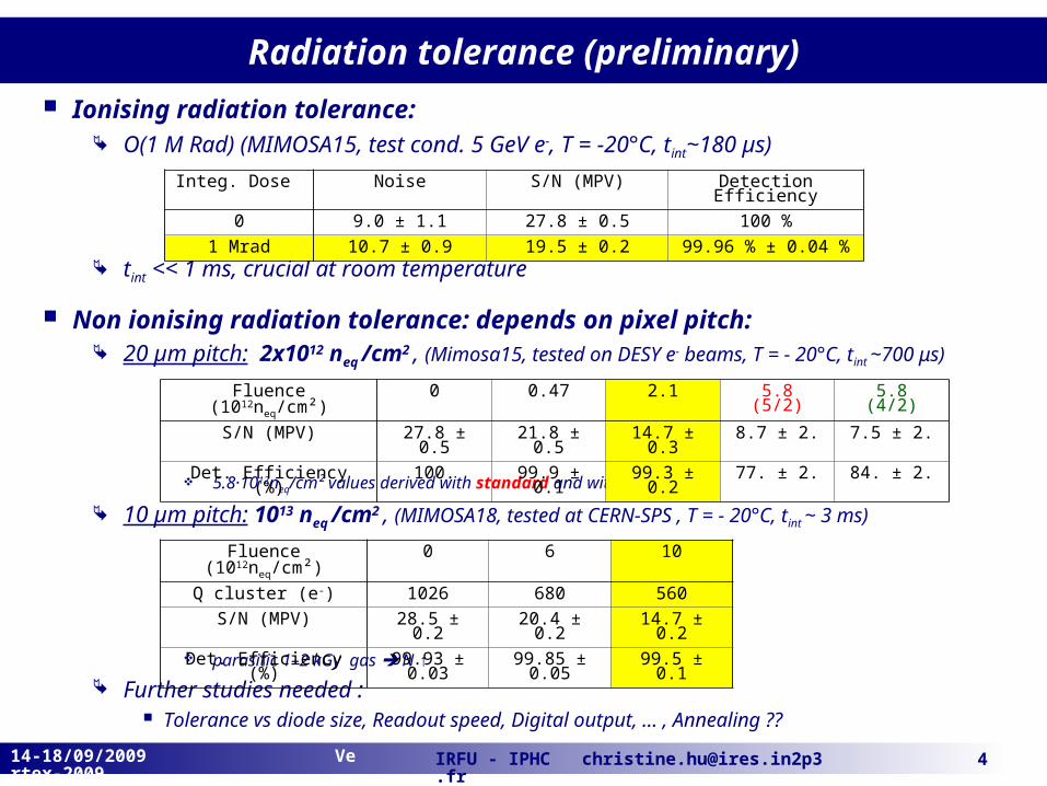
Radiation tolerance (preliminary)
Ionising radiation tolerance: O(1 M Rad) (MIMOSA15, test cond. 5 GeV e-, T = -20°C, tint~180 µs)
tint << 1 ms, crucial at room temperature
Non ionising radiation tolerance: depends on pixel pitch: 20 µm pitch: 2x10¹² neq /cm2 , (Mimosa15, tested on DESY e- beams, T = - 20°C, tint ~700 μs)
5.8·1012neq/cm² values derived with standard and with soft cuts
10 µm pitch: 1013 neq /cm2 , (MIMOSA18, tested at CERN-SPS , T = - 20°C, t int ~ 3 ms)
parasitic 1–2 kGy gas N ↑
Further studies needed : Tolerance vs diode size, Readout speed, Digital output, ... , Annealing ??
Integ. Dose Noise S/N (MPV) Detection Efficiency
0 9.0 ± 1.1 27.8 ± 0.5 100 %
1 Mrad 10.7 ± 0.9 19.5 ± 0.2 99.96 % ± 0.04 %
Fluence (1012neq/cm²) 0 0.47 2.1 5.8 (5/2) 5.8 (4/2)
S/N (MPV) 27.8 ± 0.5 21.8 ± 0.5 14.7 ± 0.3 8.7 ± 2. 7.5 ± 2.
Det. Efficiency (%) 100. 99.9 ± 0.1 99.3 ± 0.2 77. ± 2. 84. ± 2.
Fluence (1012neq/cm²)
0 6 10
Q cluster (e-) 1026 680 560
S/N (MPV) 28.5 ± 0.2 20.4 ± 0.2 14.7 ± 0.2
Det. Efficiency (%) 99.93 ± 0.03 99.85 ± 0.05 99.5 ± 0.1
IRFU - IPHC [email protected] 514-18/09/2009 Vertex-2009
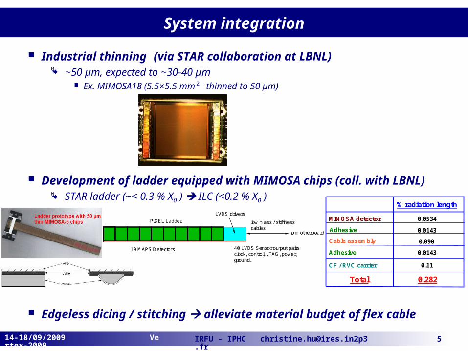
System integration
Industrial thinning (via STAR collaboration at LBNL) ~50 µm, expected to ~30-40 µm
Ex. MIMOSA18 (5.5×5.5 mm² thinned to 50 μm)
Development of ladder equipped with MIMOSA chips (coll. with LBNL) STAR ladder (~< 0.3 % X0 ) ILC (<0.2 % X0 )
Edgeless dicing / stitching alleviate material budget of flex cableIRFU - IPHC [email protected] 718-21/05/2009 FEE09
0.282Total
0.11CF / RVC carrier
0.0143Adhesive
0.090Cable assembly
0.0143Adhesive
0.0534MIMOSA detector
% radiation length
PIXEL Ladder
40 LVDS Sensor output pairs clock, control, JTAG, power,ground.
10 MAPS Detectors
low mass / stiffnesscables
to motherboard
LVDS drivers
IRFU - IPHC [email protected] 614-18/09/2009 Vertex-2009
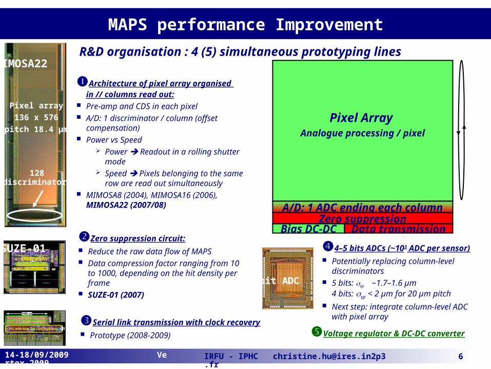
MAPS performance Improvement
SUZE-01
MIMOSA22
Pixel array
136 x 576
pitch 18.4 µm
128discriminators
5-bit ADC
Pixel Array Analogue processing / pixel
A/D: 1 ADC ending each columnZero suppression
Bias DC-DC Data transmission
R&D organisation : 4 (5) simultaneous prototyping lines
4–5 bits ADCs (~103 ADC per sensor) Potentially replacing column-level
discriminators 5 bits: sp ~1.7–1.6 µm
4 bits: sp < 2 µm for 20 µm pitch Next step: integrate column-level ADC
with pixel array
Zero suppression circuit: Reduce the raw data flow of MAPS Data compression factor ranging from 10
to 1000, depending on the hit density per frame
SUZE-01 (2007)
Architecture of pixel array organised in // columns read out:
Pre-amp and CDS in each pixel A/D: 1 discriminator / column (offset
compensation) Power vs Speed
Power Readout in a rolling shutter mode
Speed Pixels belonging to the same row are read out simultaneously
MIMOSA8 (2004), MIMOSA16 (2006), MIMOSA22 (2007/08)
Serial link transmission with clock recovery Prototype (2008-2009) Voltage regulator & DC-DC converter
IRFU - IPHC [email protected] 714-18/09/2009 Vertex-2009
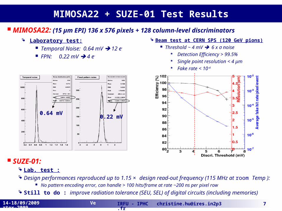
MIMOSA22 + SUZE-01 Test Results
MIMOSA22: (15 µm EPI) 136 x 576 pixels + 128 column-level discriminators
SUZE-01: Lab. test : Design performances reproduced up to 1.15 × design read-out frequency (115 MHz at room Temp ):
No pattern encoding error, can handle > 100 hits/frame at rate ~200 ns per pixel row
Still to do : improve radiation tolerance (SEU, SEL) of digital circuits (including memories)
0.64 mV0.22 mV
Laboratory test: Temporal Noise: 0.64 mV 12 e-
FPN: 0.22 mV 4 e-
Beam test at CERN SPS (120 GeV pions) Threshold ~ 4 mV 6 x σ noise
Detection Efficiency > 99.5% Single point resolution < 4 µm Fake rate < 10-4
IRFU - IPHC [email protected] 814-18/09/2009 Vertex-2009
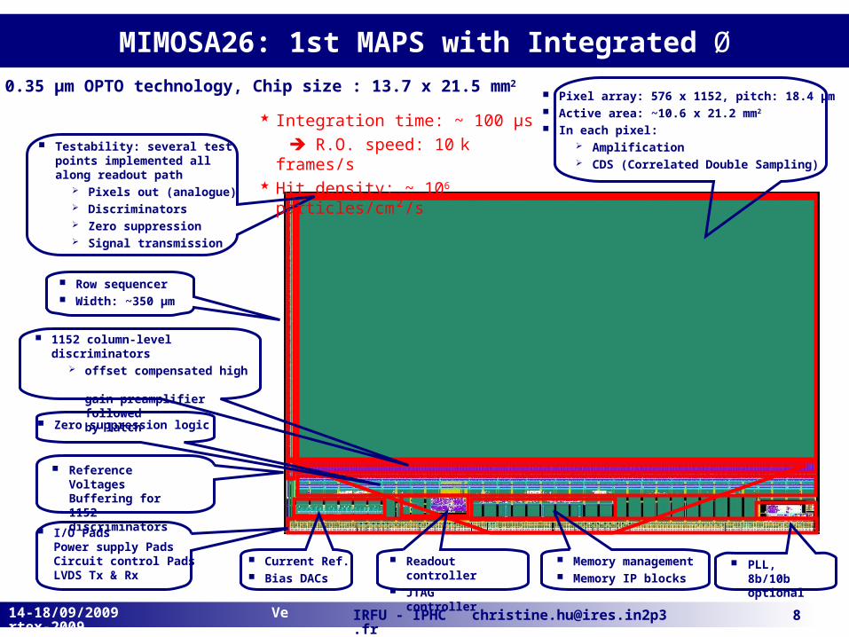
MIMOSA26: 1st MAPS with Integrated Ø
Pixel array: 576 x 1152, pitch: 18.4 µm Active area: ~10.6 x 21.2 mm2
In each pixel: Amplification CDS (Correlated Double Sampling)
1152 column-level discriminators offset compensated high
gain preamplifier followedby latch
Zero suppression logic
Memory management Memory IP blocks
Readout controller JTAG controller
Current Ref. Bias DACs
Row sequencer Width: ~350 µm
I/O PadsPower supply PadsCircuit control PadsLVDS Tx & Rx
CMOS 0.35 µm OPTO technology, Chip size : 13.7 x 21.5 mm2
Testability: several test points implemented all along readout path
Pixels out (analogue) Discriminators Zero suppression Signal transmission
Reference Voltages Buffering for 1152 discriminators
PLL, 8b/10b optional
Integration time: ~ 100 µs R.O. speed: 10 k frames/s Hit density: ~ 106
particles/cm²/s

IRFU - IPHC [email protected] 914-18/09/2009 Vertex-2009
Test MIMOSA26 (Lab. + beam test)
Measured temporal noise = 0.6-0.7 mV and FPN = 0.3-0.4 mV for pixel array with its associated discriminators.
These values are equivalent to those obtained with Mimosa22. It shows a good uniformity of the whole 576 x 1152 pixels with the 1152 discriminators
~ 30 MIMOSA26 chips are tested (only 1 "dead") The characterization of Mimosa26 is complemented by the beam tests (Sept. 2009)
6 MIMOSA26 chips are running simultaneously at nominal speed Tracking successful data analysis is underway, preliminary results show similar performances as MIMOSA22
Entries 576 x 288
Mean 0.64 mV
RMS 0.07 mV
Noise distribution [mV] Threshold distribution [mV]
Entries 576 x 288
Mean -0.93 mV
RMS 0.29 mV
IRFU - IPHC [email protected] 1014-18/09/2009 Vertex-2009
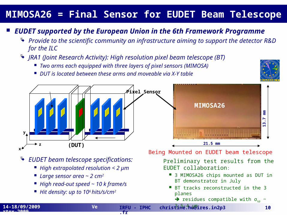
MIMOSA26 = Final Sensor for EUDET Beam Telescope
EUDET supported by the European Union in the 6th Framework Programme Provide to the scientific community an infrastructure aiming to support the detector R&D
for the ILC JRA1 (Joint Research Activity): High resolution pixel beam telescope (BT)
Two arms each equipped with three layers of pixel sensors (MIMOSA) DUT is located between these arms and moveable via X-Y table
EUDET beam telescope specifications: High extrapolated resolution < 2 µm Large sensor area ~ 2 cm2
High read-out speed ~ 10 k frame/s Hit density: up to 106 hits/s/cm2
(DUT)
Pixel Sensor
xz
y
21.5 mm
13.7
mm
MIMOSA26
Being Mounted on EUDET beam telescope
Preliminary test results from the EUDET collaboration:
3 MIMOSA26 chips mounted as DUT in BT demonstrator in July
BT tracks reconstructed in the 3 planes residues compatible with σsp ~ 3.5-4 μm
IRFU - IPHC [email protected] 1114-18/09/2009 Vertex-2009
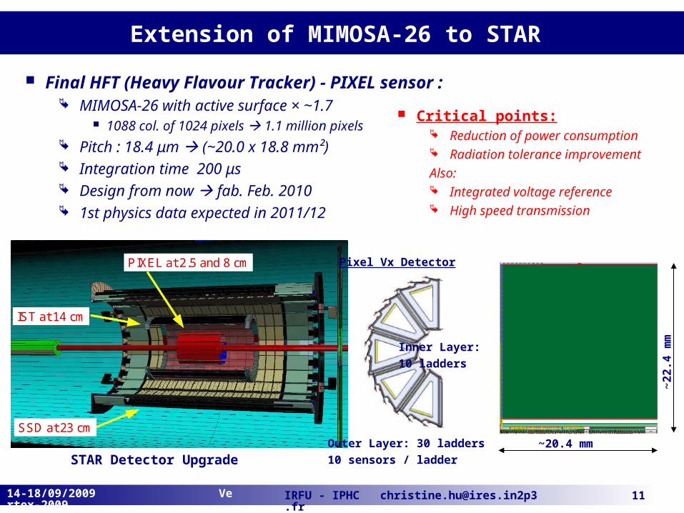
Extension of MIMOSA-26 to STAR
Final HFT (Heavy Flavour Tracker) - PIXEL sensor : MIMOSA-26 with active surface × ~1.7
1088 col. of 1024 pixels 1.1 million pixels Pitch : 18.4 μm (~20.0 x 18.8 mm²) Integration time 200 μs Design from now fab. Feb. 2010 1st physics data expected in 2011/12
PIXEL at 2.5 and 8 cm
IST at 14 cm
SSD at 23 cm
STAR Detector Upgrade
Inner Layer:
10 ladders
Outer Layer: 30 ladders
10 sensors / ladder
~20.4 mm
~2
2.4
mm
Pixel Vx Detector
Critical points: Reduction of power consumption Radiation tolerance improvement
Also: Integrated voltage reference High speed transmission
IRFU - IPHC [email protected] 1214-18/09/2009 Vertex-2009
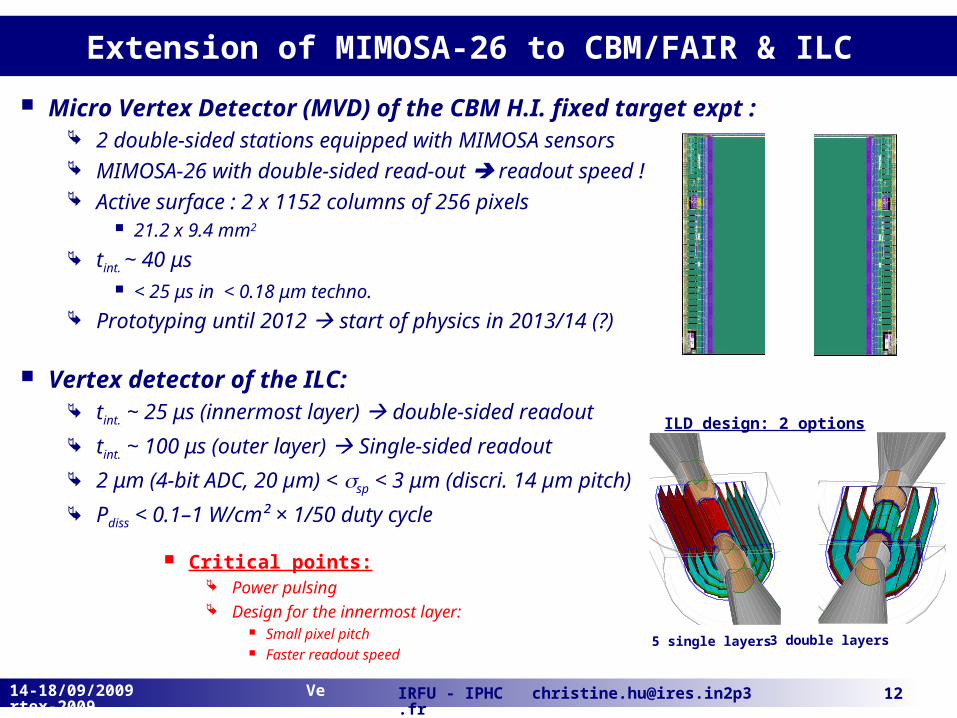
Extension of MIMOSA-26 to CBM/FAIR & ILC
Micro Vertex Detector (MVD) of the CBM H.I. fixed target expt : 2 double-sided stations equipped with MIMOSA sensors MIMOSA-26 with double-sided read-out readout speed ! Active surface : 2 x 1152 columns of 256 pixels
21.2 x 9.4 mm2
tint. ~ 40 μs < 25 μs in < 0.18 μm techno.
Prototyping until 2012 start of physics in 2013/14 (?)
Vertex detector of the ILC: tint. ~ 25 μs (innermost layer) double-sided readout
tint. ~ 100 μs (outer layer) Single-sided readout
2 μm (4-bit ADC, 20 µm) < sp < 3 μm (discri. 14 µm pitch)
Pdiss < 0.1–1 W/cm² × 1/50 duty cycle
Critical points: Power pulsing Design for the innermost layer:
Small pixel pitch Faster readout speed
5 single layers 3 double layers
ILD design: 2 options
IRFU - IPHC [email protected] 1314-18/09/2009 Vertex-2009
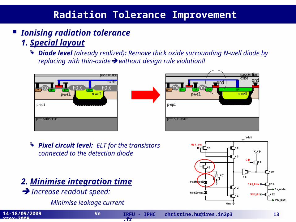
Radiation Tolerance Improvement
Ionising radiation tolerance 1. Special layout
Diode level (already realized): Remove thick oxide surrounding N-well diode by replacing with thin-oxide without design rule violation!!
Pixel circuit level: ELT for the transistors connected to the detection diode
2. Minimise integration time Increase readout speed:
Minimise leakage current
PWR_On
Clp
Vdd!
Gnd!
V_clp
Slct_Row
Slct_Gr
Gr_node
Pix_Out
Nwell/Pepi
Pdiff/Nwell
M1
M2
M3
M6M4
M5
M7M8
M9
M10
M11
M12
PWR_On Clp Slct_Row
Slct_Gr
V_clpVdd! Vdd!
Michal Szelezniak - PhD thesis defense - 25 February 2008
1515
I ncreased tolerance to ionizing radiation
standard diode layoutstandard diode layout
thinthin--oxide diode layoutoxide diode layout
Shot Noise Contribution @ 30Shot Noise Contribution @ 30°°C C and @4 ms integration timeand @4 ms integration time
ENCENCshotshot = 39 electrons= 39 electrons
ENCENCshotshot = 12 electrons= 12 electrons
n+n+p+ n+p-well
depleted region
p++ substrate
passivation
oxide
p-epi
n-well
FOXFOXFOX
n+n+p+p-well
depleted region
p++ substrate
passivationoxide
p-epi
n-well
FOX FOX n+
gnd gnd
n+
IRFU - IPHC [email protected] 1414-18/09/2009 Vertex-2009
Radiation Tolerance Improvement
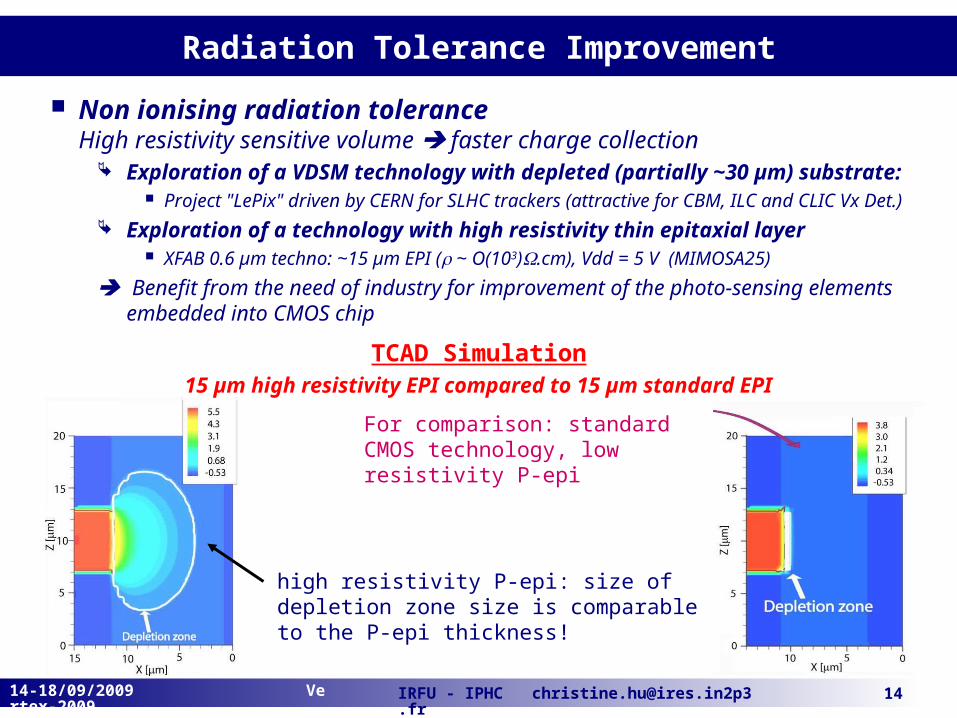
Non ionising radiation toleranceHigh resistivity sensitive volume faster charge collection
Exploration of a VDSM technology with depleted (partially ~30 µm) substrate: Project "LePix" driven by CERN for SLHC trackers (attractive for CBM, ILC and CLIC Vx Det.)
Exploration of a technology with high resistivity thin epitaxial layer XFAB 0.6 µm techno: ~15 µm EPI ( ~ O(103).cm), Vdd = 5 V (MIMOSA25)
Benefit from the need of industry for improvement of the photo-sensing elements embedded into CMOS chip
For comparison: standard CMOS technology, low resistivity P-epi
high resistivity P-epi: size of depletion zone size is comparable to the P-epi thickness!
TCAD Simulation15 µm high resistivity EPI compared to 15 µm standard EPI
IRFU - IPHC [email protected] 1514-18/09/2009 Vertex-2009
Landau MP (in electrons) versus cluster sizeLandau MP (in electrons) versus cluster size0 neq/cm²
0.3 x 10¹³ neq/cm²
1.3 x 10¹³ neq/cm²
3 x 10¹³ neq/cm²
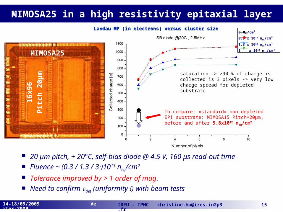
MIMOSA25 in a high resistivity epitaxial layer
20 μm pitch, + 20°C, self-bias diode @ 4.5 V, 160 μs read-out time Fluence ~ (0.3 / 1.3 / 3·)1013 neq/cm2 Tolerance improved by > 1 order of mag. Need to confirm det (uniformity !) with beam tests
16x9
6
Pit
ch 2
0µm
MIMOSA25
To compare: «standard» non-depleted EPI substrate: MIMOSA15 Pitch=20µm, before and after 5.8x10¹² neq/cm2
saturation -> >90 % of charge is collected is 3 pixels -> very low charge spread for depleted substrate
IRFU - IPHC [email protected] 1614-18/09/2009 Vertex-2009
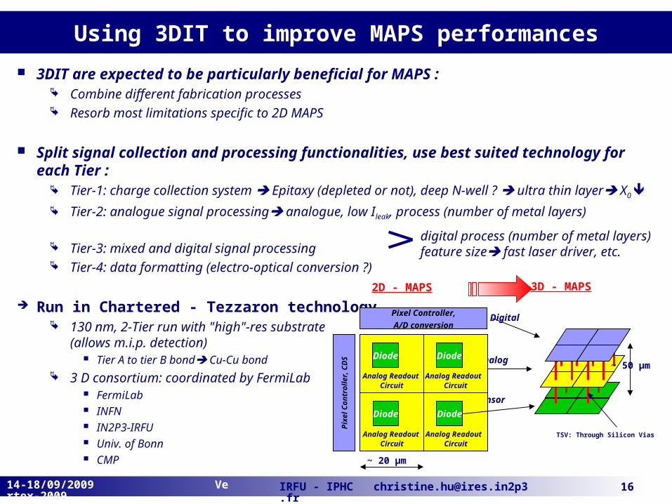
Using 3DIT to improve MAPS performances
3DIT are expected to be particularly beneficial for MAPS : Combine different fabrication processes Resorb most limitations specific to 2D MAPS
Split signal collection and processing functionalities, use best suited technology for each Tier :
Tier-1: charge collection system Epitaxy (depleted or not), deep N-well ? ultra thin layer X0 Tier-2: analogue signal processing analogue, low Ileak, process (number of metal layers)
Tier-3: mixed and digital signal processing Tier-4: data formatting (electro-optical conversion ?)
Run in Chartered - Tezzaron technology 130 nm, 2-Tier run with "high"-res substrate
(allows m.i.p. detection) Tier A to tier B bond Cu-Cu bond
3 D consortium: coordinated by FermiLab FermiLab INFN IN2P3-IRFU Univ. of Bonn CMP
digital process (number of metal layers)feature size fast laser driver, etc.
Analog Readout Circuit
Diode
Pixel Controller,
A/D conversion
Pix
el C
on
tro
ller
, C
DS
Digital
Analog
Sensor
~ 50 µmAnalog Readout
Circuit
Diode
~ 20 µm
Analog Readout Circuit
Diode
Analog Readout Circuit
Diode
TSV: Through Silicon Vias
2D - MAPS 3D - MAPS
IRFU - IPHC [email protected] 1714-18/09/2009 Vertex-2009
IPHC & IRFU 3D MAPS
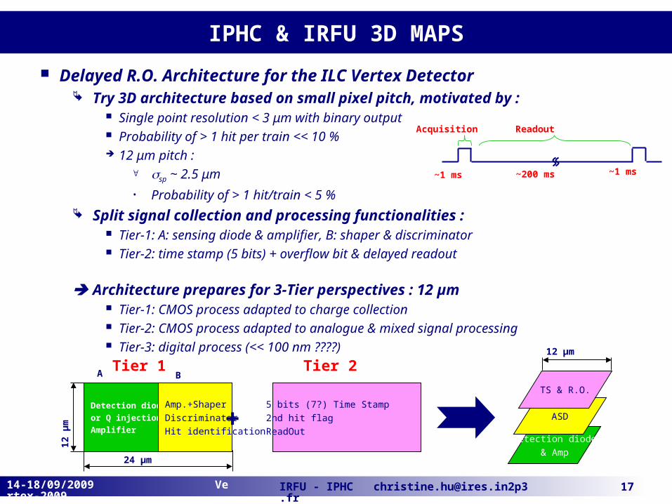
Delayed R.O. Architecture for the ILC Vertex Detector Try 3D architecture based on small pixel pitch, motivated by :
Single point resolution < 3 μm with binary output Probability of > 1 hit per train << 10 % 12 μm pitch :
sp ~ 2.5 μm
• Probability of > 1 hit/train < 5 % Split signal collection and processing functionalities :
Tier-1: A: sensing diode & amplifier, B: shaper & discriminator Tier-2: time stamp (5 bits) + overflow bit & delayed readout
Architecture prepares for 3-Tier perspectives : 12 µm Tier-1: CMOS process adapted to charge collection Tier-2: CMOS process adapted to analogue & mixed signal processing Tier-3: digital process (<< 100 nm ????)
~1 ms ~1 ms~200 ms
Acquisition Readout
Detection diode
or Q injection
Amplifier
Amp.+Shaper
Discriminator
Hit identification
12 µ
m
24 µm
5 bits (7?) Time Stamp
2nd hit flag
ReadOut
Tier 1 Tier 2A B
+Detection diode
& Amp
ASD
TS & R.O.
12 µm
IRFU - IPHC [email protected] 1814-18/09/2009 Vertex-2009
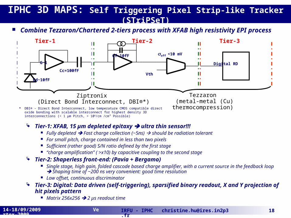
IPHC 3D MAPS: Self Triggering Pixel Strip-like Tracker (STriPSeT)
Combine Tezzaron/Chartered 2-tiers process with XFAB high resistivity EPI process
Tier-1: XFAB, 15 µm depleted epitaxy ultra thin sensor!!! Fully depleted Fast charge collection (~5ns) should be radiation tolerant For small pitch, charge contained in less than two pixels Sufficient (rather good) S/N ratio defined by the first stage “charge amplification” ( >x10) by capacitive coupling to the second stage
Tier-2: Shaperless front-end: (Pavia + Bergamo) Single stage, high gain, folded cascode based charge amplifier, with a current source in the feedback loop
Shaping time of ~200 ns very convenient: good time resolution Low offset, continuous discriminator
Tier-3: Digital: Data driven (self-triggering), sparsified binary readout, X and Y projection of hit pixels pattern
Matrix 256x256 2 µs readout time
Tier-1 Tier-2 Tier-3
Cd~10fF
G~1
Cc=100fF
Cf~10fF off <10 mV
Digital RD
Vth
Ziptronix (Direct Bond Interconnect, DBI®*)
Tezzaron (metal-metal (Cu)
thermocompression) DBI® – Direct Bond Interconnect, low temperature CMOS compatible direct oxide bonding with scalable interconnect for highest density 3D interconnections (< 1 µm Pitch, > 108/cm /cm² Possible)
IRFU - IPHC [email protected] 1914-18/09/2009 Vertex-2009
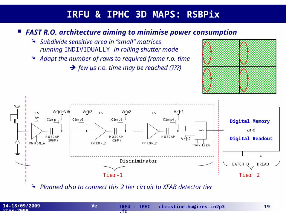
IRFU & IPHC 3D MAPS: RSBPix
FAST R.O. architecture aiming to minimise power consumption Subdivide sensitive area in ”small” matrices
running INDIVIDUALLY in rolling shutter mode Adapt the number of raws to required frame r.o. time
few µs r.o. time may be reached (???)
Planned also to connect this 2 tier circuit to XFAB detector tier
MOSCAP (20fF)
Vclp2
PWRON_D
MOSCAP
Vclp2
PWRON_D
Latch
Latch
Clamp1 Clamp4
Vclp2
Vclp2
Clamp0
Track
CS CS
Clamp
MOSCAP (100fF)
Vclp1+Vth
PWRON_A
Vrst
Av ~ 4
CS
Tier-1 Tier-2
Digital Memory
and
Digital Readout
DiscriminatorDREADLATCH_D
IRFU - IPHC [email protected] 2014-18/09/2009 Vertex-2009
Conclusion
2D MAPS have reached necessary prototyping maturity for real scale applications :
Beam telescopes allowing for sp ~ few μm & 106 particles/cm²/s
Vertex detectors requiring high resolution & very low material budget
The emergence of fabrication processes with depleted epitaxy / substrate opens the door to :
Substantial improvements in read-out speed and non-ionising radiation tolerance "Large pitch" applications trackers (e.g. Super LHC )
Translation to 3D integration technology : Resorb most limitations specific to 2D MAPS
T type & density, peripheral insensitive zone, combination of different CMOS processes Offer an improved read-out speed : O(μs) ! Many difficulties to overcome (ex. heat, power) R&D in progress 2009/10 important step for validation of this promising
technology
Top Related