


Languages
Pages
Legal

INV ITEDP A P E R
Flexible Electronics: The NextUbiquitous PlatformThis paper reviews thin-film materials and technologies for flexible electronics
and considers future applications in healthcare, the automotive industry,
human–machine interfaces, mobile devices, and other environments.
By Arokia Nathan, Fellow IEEE, Arman Ahnood, Matthew T. Cole,
Sungsik Lee, Member IEEE, Yuji Suzuki, Pritesh Hiralal, Francesco Bonaccorso,
Tawfique Hasan, Luis Garcia-Gancedo, Andriy Dyadyusha, Samiul Haque,
Piers Andrew, Stephan Hofmann, James Moultrie, Daping Chu, Andrew J. Flewitt,
Andrea C. Ferrari, Michael J. Kelly, John Robertson, Fellow IEEE,
Gehan A. J. Amaratunga, and William I. Milne
ABSTRACT | Thin-film electronics in its myriad forms has
underpinned much of the technological innovation in the fields
of displays, sensors, and energy conversion over the past four
decades. This technology also forms the basis of flexible elec-
tronics. Here we review the current status of flexible electronics
and attempt to predict the future promise of these pervading
technologies in healthcare, environmental monitoring, displays
and human–machine interactivity, energy conversion, manage-
ment and storage, and communication and wireless networks.
KEYWORDS | Computation; displays; energy generation; energy
storage; flexible substrates; healthcare; human–machine inter-
activity; lab-on-chip; mobility; sensors; thin-film technology;
wireless networks
I . INTRODUCTION
Ever evolving advances in thin-film materials and devices
have fueled many of the developments in the field of
flexible electronics. These advances have been comple-
mented with the development of new integration process-
es, enabling wafer-scale processes to be combined with
flexible substrates. This has resulted in a wealth ofdemonstrators in recent years. Following substantial
development and optimization over many decades, thin-
film materials can now offer a host of advantages such as
low cost and large area compatibility, and high scalability
in addition to seamless heterogeneous integration.
Diodes and transistors are two of the most common
active thin-film devices used in a wide range of digital and
analog circuits, as well as for detection and energy gener-ation. While they have been successfully used in flexible
platforms, their performance and applicability in systems
is limited by a number of factors, inevitability requiring
Manuscript received February 18, 2012; accepted February 20, 2012. Date of current
version May 10, 2012. The work of A. Nathan was supported by the European Union
project ORAMA and the Royal Society Wolfson Research Merit Award. The work of
M. T. Cole was supported by the St. Edmund’s College, Cambridge University and the
Isaac Newton Trust, Trinity College, Cambridge University. The work of A. J. Flewitt was
supported by the EPSRC through grant EP/F063865/1. The work of T. Hasan was
supported by the King’s College, Cambridge University, Cambridge, U.K. and the Royal
Academy of Engineering. The work of D. P. Chu was supported by the EPSRC Platform
Grant (Liquid Crystal Photonics). The work of A. C. Ferrari was supported by the
European Research Council project NANOPOTS, European Union projects RODIN and
GENIUS, and a Royal Society Wolfson Research Merit Award.
A. Nathan and A. Ahnood are with Centre for Advanced Photonics and Electronics,
Department of Engineering, Cambridge University, Cambridge CB3 0FA, U.K.
(e-mail: [email protected]; [email protected]).
M. T. Cole, L. Garcia-Gancedo, S. Hofmann, A. J. Flewitt, M. J. Kelly, J. Robertson,and W. I. Milne are with the Electronic Devices and Materials Group, Department of
Engineering, Cambridge University, Cambridge CB3 0FA, U.K. (e-mail:
[email protected]; [email protected]; [email protected]; [email protected];
[email protected]; [email protected]; [email protected]).
S. Lee and Y. Suzuki are with London Centre for Nanotechnology, University College
London, London WC1H 0AH, U.K. (e-mail: [email protected]; [email protected]).
P. Hiralal and G. A. J. Amaratunga are with the Electronics, Power and Energy
Conversion Group, Department of Engineering, Cambridge University, Cambridge
CB3 0FA, U.K. (e-mail: [email protected]; [email protected]).
F. Bonaccorso, T. Hasan, and A. C. Ferrari are with the Nanomaterials and
Spectroscopy Group, Department of Engineering, Cambridge University, Cambridge
CB3 0FA, U.K. (e-mail: [email protected]; [email protected]; [email protected]).
A. Dyadyusha and D. Chu are with the Photonics and Sensors Group, Department of
Engineering, Cambridge University, Cambridge CB3 0FA, U.K. (e-mail:
[email protected]; [email protected]).
S. Haque and P. Andrew are with Nokia Research Center, Cambridge CB3 0FA, U.K.
(e-mail: [email protected]; [email protected]).
J. Moultrie is with the Design Management Group, Institute for Manufacturing,
Cambridge University, Cambridge CB3 0FS, U.K. (e-mail: [email protected]).
Digital Object Identifier: 10.1109/JPROC.2012.2190168
1486 Proceedings of the IEEE | Vol. 100, May 13th, 2012 0018-9219/$31.00 �2012 IEEE
use of exotic device architectures, consisting of highlyoptimized geometries combined with integration of novel
materials. This has often facilitated tailoring of the elec-
tronic properties toward particular applications that
demonstrate vast improvements in form factor, though
typically at significant financial cost, which is unacceptable
at the en masse scale. Though such Bone-off[ devices are of
significant interest to the academic community, little has
been achieved in the way of full-scale system integration.Indeed large-area simple devices, such as resistive and
inductive networks, have been demonstrated. In order to
achieve the goal of full-system integration in Bnext-
generation flexible systems[ a paradigm shift in design
and fabrication is necessary. The ethos of the conventional
integrated circuit (IC) manufacturer must be adjusted.
Notwithstanding, improved understanding in the material
growth/deposition, integration, and processing must cer-tainly be advanced and such knowledge is often derived via
the speculative academic. Reduced cost, large area, roll-to-
roll, and flexible systems, such as low-cost flexible
displays, require conformal, distributed, and integrated
functionality, which is hitherto unavailable from more
traditional brittle material and device platforms. Such
functionality will certainly offer disruptive alternatives for
more established technologies that cumulatively representperhaps one of the world’s largest economic markets in
human history, while also facilitating the development of
distinctly niche markets that exploit these new capabilities
in truly unexpected applications. Just as the IC replaced
discrete circuit board electronics, flexible electronics
will almost inevitablyVby virtue of the ever-demanding
end-userVsupersede solid-state ICs, in particular, appli-
cations where form factors are important; though thematerials, technologies and devices necessary to achieve
this are still largely unclear to many.
This paper reviews the materials, design issues, and
technologies for next-generation flexible electronics, and
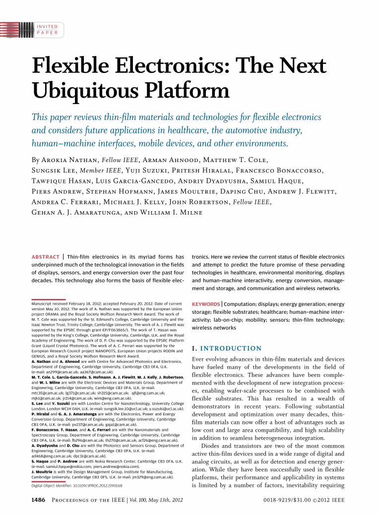
primarily considers future applications therein (Fig. 1).
We summarize the potential of flexible thin-film devices,
the limitations of particular materials with regard to
manufacturability, deposition issues, and monitoringtechniques that must be resolved and improved prior to
their wide adoption, with particular reference to a new
class of materials available to system designersVthe
nanomaterials. This paper is foremost organized from the
standpoint of applications, with some of the more
pertinent questions posing the materials engineer intro-
duced to stimulate discussion. We present examples of
potential applications of flexible electronics in varioussocietal sectors, including: healthcare; the automotive
industry; human–machine interfaces; mobile communi-
cations and computing platforms; embedded systems in
both living and hostile environments; as well as market-
specific applications, such as: human–machine interactiv-
ity, energy storage and generation, mobile communications
and networking, while touching on the application of
flexible electronics on ubiquitous computing platforms
throughout.
II . MATERIALS, TECHNOLOGIES, ANDINTEGRATION PROCESSES
The fundamental properties of thin-film materials, as well
as the quality of various device interfaces, give rise to
inherent limitations in device performance. For instance,
consider the ring oscillator. As one of the most essential
building blocks in many systems, it is fundamental to many
emerging technologies, such as radio-frequency identifi-cation (RFIDs) tagging. A large number of design param-
eters influence the oscillation frequency of ring oscillators.
These include geometric attributes, parasitic capacitance,
and the supply voltage. However, these adjustments are
often dwarfed by the inherent performance limitations of
the transistors. Considering the field-effect mobility as a
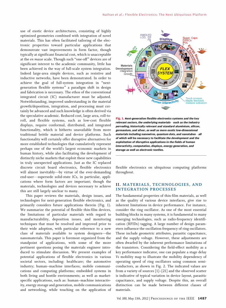
key performance indicator, one can populate a stage delay
Vs mobility map to illustrate the mobility dependency ofoperating speed of ring oscillators using common semi-
conductors, as shown in Fig. 2. The indicated values are
from a variety of sources [1]–[21] and the observed scatter
is indicative of typical variation in device layout, parasitic
capacitance, and supply voltage. Despite this, an overall
distinction can be made between different classes of
materials.
Fig. 1. Next-generation flexible electronics systems and the key
relevant sectors, the underlying materialsVsuch as the industry
pervading, historically relevant and standard aluminium, silicon,
germanium, and silver, as well as more exotic low-dimensional
materials including nanowires, quantum dots, and nanotubesVall
of which will be necessary to facilitate the development and the
exploitation of disruptive applications in the fields of human
interactivity, computation, displays, energy generation, and
storage as well as electronic textiles.
Nathan et al.: Flexible Electronics: The Next Ubiquitous Platform
Vol. 100, May 13th, 2012 | Proceedings of the IEEE 1487
The field-effect mobility itself is a function of a
number of parameters. As well as material’s band mobility
[22] and the quality of the dielectric/semiconductor in-
terface, it is also influenced by the contact resistance [23],[24] and the dynamic characteristics of the thin-film
transistor (TFT) [25].
Although it is desirable to use thin-film materials with
the highest possible mobility, issues of cost and scalability
play critical roles in material selection. For instance, the
two highest mobility materials (Fig. 2) are polycrystalline
silicon (poly-Si) and semiconducting metal oxides (MOx).
Currently, MOx are costly due to the global localizationand shortage of indium [26], [27]. Despite the availability
of low-cost Si, the fabrication process of poly-Si is also
rather costly, due to postdeposition processing require-
ments in large-area applications [28]–[30].
Incorporating nanowires (NWs), carbon nanotubes
(CNTs), graphene or other nanomaterials within semicon-
ducting thin films allow tailoring of their properties [31],
[32]. Devices based on such composites typically exhibitenhanced electrical performance, such as higher field-
effect mobility and subthreshold slope, leading to lower
operating voltagesVan important consideration in low-
power circuit design. Moreover, the composite nature of
the thin films affects their mechanical properties [33], [34],
and the TFT durability when subjected to mechanical stress:
an essential requirement for truly flexible electronics.
In addition to the aforementioned device performancesand costs, their stability when subjected to prolonged
electrical [35] or optical bias [36], [37] is critically impor-
tant. For instance, although Fig. 2 depicts a marginal
performance variation between microcrystalline (mc-Si),
nanocrystalline (nc-Si), and amorphous silicon (a-Si) on
the global scale, the stability of TFTs when subjected to
electrical bias and/or illumination is considerably differ-
ent. Through engineering mixed-phased heterogeneousmaterials, it is possible to achieve higher degrees of stabi-
lity compared with conventional a-Si [38].
Recently, novel fabrication techniques have allowed
TFTs to harness the potential of 1-D semiconductors,
such as CNT and NWs, as well as 2-D semiconductors
and dielectrics such as graphene [39], [40] and molyb-
denum disulfide (MoS2) [41] and hexagonal boron nitride
(h-BN) monolayers [42]. These devices exhibit remark-able properties, though further progress is critical before
they can be commercialized in flexible circuits and integ-
rated systems.
Fabrication methods also have an important effect on
the characteristics, cost, and stability. For example, instead
of using a high mobility material to achieve high device
transconductance, it is possible to adjust the architecture.
Employing short channel lengths is one way to achievethis. In conventional planar TFTs, the channel length is
ultimately limited by the diffraction limit in the photoli-
thography process. Vertical transistors, where the channel
length is set by the thickness of the semiconductor, have
been demonstrated as to achieve submicrometer channel
lengths, paving the way for high transconductance devices
using conventional materials such as a-Si.[43].
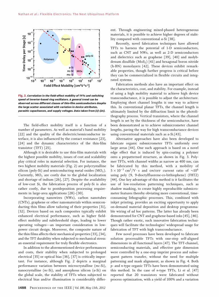
Alternative approaches have also been developed tofabricate organic submicrometer TFTs uniformly over
large areas [44]. One such approach is based on a novel
edge effect that is induced by spin-coating a polymer
onto a prepatterned structure, as shown in Fig. 3. Poly-
mer TFTs, with channel widths as narrow as 400 nm, can
be fabricated by this method, with a mobility of
5 � 10�3 cm2=V � s and on/off current ratio of �106
using poly (9, 9-dioctylfluorene-co-bithiophene) (F8T2)[44]. One key advantage of this method is it facilitates the
use of low-resolution patterning techniques, such as
shadow masking, to create highly reproducible submicro-
meter features thereby obviating more conventional, time-
consuming lithographic processes. This, combined with
inkjet printing, provides an exciting opportunity to apply
on-demand material deposition and desktop programma-
ble wiring of ad hoc patterns. The latter has already beendemonstrated for CNT and graphene-based inks [45], [46].
Though rather exotic, such innovative fabrication techni-
ques will facilitate the technologies’ widespread usage for
fabrication of TFT with high transconductance.
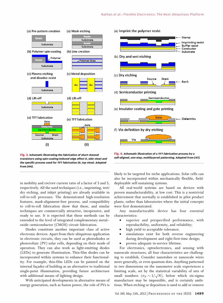
Few novel processes have been developed to fabricate
solution processable TFTs with one-step self-aligned
dimensions in all functional layers [47]. The TFT-channel,
semiconducting materials, and effective gate dimensionwere controlled by a one-step imprint process and subse-
quent pattern transfer, without the need for multiple
patterning and mask alignment, as shown in Fig. 4. Both
p- and n-type organic TFTs have been demonstrated using
this method. In the case of n-type TFTs, Li et al. [47]
reported that 20 transistors were fabricated without
process optimization, with a yield of 100% and a variation
Fig. 2. Correlation in the field-effect mobility of TFTs and switching
speed of inverter-based ring oscillators. A general trend can be
observed across different classes of thin-film semiconductors despite
the large scatter associated with variation in device attributes,
parasitic capacitances, and supply voltages. Data taken from [1]–[21].
Nathan et al.: Flexible Electronics: The Next Ubiquitous Platform
1488 Proceedings of the IEEE | Vol. 100, May 13th, 2012
in mobility and on/off current ratio of a factor of 3 and 5,
respectively. All the used techniques (i.e., imprinting, wet/
dry etching, and inkjet printing) are already available in
roll-to-roll processes. The demonstrated high-resolution
features, mask-alignment-free process, and compatibility
to roll-to-roll fabrication show that these, and similar
techniques are commercially attractive, inexpensive, andready to use. It is expected that these methods can be
extended to the level of integrated complementary metal–
oxide–semiconductor (CMOS) circuit fabrication.
Diodes constitute another important class of active
electronic devices. Apart from their ubiquitous application
in electronic circuits, they can be used as photodiodes or
photovoltaic (PV) solar cells, depending on their mode of
operation. They can also work as light-emitting diodes(LEDs) to generate illumination. Thin-film diodes can be
incorporated within systems to enhance their functional-
ity. For example, thin-film LEDs can be painted on the
internal facades of building as an alternative to traditional
single-point illumination, providing future architecture
with additional means of lighting design.
With anticipated developments in alternative means of
energy generation, such as fusion power, the role of PVs is
likely to be targeted for niche applications. Solar cells can
also be incorporated within mechanically flexible, field-deployable self-sustaining systems.
All real-world systems are based on devices with
proven manufacturability, at low cost. This is a nontrivial
achievement that normally is established in pilot product
plants, rather than laboratories where the initial concepts
were first demonstrated.
Any manufacturable device has four essential
characteristics:• superior and prespecified performance, with
reproducibility, uniformity, and reliability;
• high yield to acceptable tolerance;
• simulations exist for both reverse engineering
during development and right-first-time design;
• proven adequate in-service lifetime.
For electronics, optoelectronics, and sensing with
nanoscale structures, all four characteristics are challeng-ing to establish. Consider nanotubes or nanoscale wires
more generally, or even quantum dots. Anything patterned
in two dimensions on the nanometer scale experiences a
limiting scale, set by the statistical variability of sets of
small numbers ð�N � 1=pNÞ, below which six-sigma
manufacture may be impossible, and is certainly ambi-
tious. When etching or deposition is used to add or remove
Fig. 4. Schematic illustration of a TFT fabrication process by a
self-aligned, one-step, multilayered patterning. Adapted from [47].Fig. 3. Schematic illustrating the fabrication of short channel
transistors using spin-coating-induced edge effect (I, side view) and
the specific process used for TFT fabrication (II, top view). Adapted
from [44].
Nathan et al.: Flexible Electronics: The Next Ubiquitous Platform
Vol. 100, May 13th, 2012 | Proceedings of the IEEE 1489
individual atoms to, or from, structures, this limit appearsat the 7-nm half-pitch. For arrays of nanometer half-pitch,
� ¼ 12%, highlighting a clearly intolerable variation for
the electronic transport or optical properties of arrays
made of elements with such intrinsic variability. Even if we
could successfully fabricate such arrays by heroic proces-
sing, at very high cost, one must noteVatom by atom with
a force microscope of sortsVthat there would never be
such an array to write, store, or read information as theelectrons and photons would leak extensively over
extremely short timescales [48].
Consider quantum wires. Adequate control over the
cross-section area from wire to wire is difficult, as it is for
any regularity in the spacing of the wires across the sub-
strate. Until these are achieved, any ideas based on any-
thing other than their prevailing bulk properties is
practically impossible. Computer models of these wiresare primitive and certainly not adequate for producing a
right-first-time designVthe incorporation of detailed
boundary conditions is inadequate, and interwire interac-
tions are not treated with any suitable regard. The grand
challenge is to produce an array, or even a single wire, that
has precisely 15% variation in its properties across an
array. Only small stresses during in-life operation are suf-
ficient to have atoms move or conductivities change, sothat 103 hours with less than 5% change in the device
operation is harder to achieve, especially if high local
powers are involved.
The same problems arise, but for different reasons,
when considering the bottom-up or self-assembly process.
Very few of the molecules used in self-assembly are avail-
able at the 5-nines (99.999%) purity level which is implied
by a six-sigma manufacturing quality. It may also be thatapproximately spherical molecules will not be suitable for
connected arraysVit is likely that the individual molecular
elements of the arrays will need Bhandles[ to assist in the
subsequent wiring of an array for electronic addressing. In
the 3–7-nm diameter range for these molecules, the ability
to align such nonspherical arrays with a sufficiently small
standard deviation in the in-plane orientation of the
Bhandles[ is also a challenge for future research.The proof of manufacturability is intimately linked
with the intrinsic physics and materials science at the
nanoscale. Any establishment of device manufacturability
must come from the science and engineering laboratory
before moving into pilot production plant. This is a culture
change which is not happening. Fewer than 1% of papers
in nanotechnology literature contain the worlds Byield,[Breproducibility,[ or Blifetime.[ It seems timely for such aculture change so that the end-to-end efficiency, i.e., from
device concept to real product, can be improved. Why
persist with the science of something that is intrinsically
unmanufacturable? However, such arguments apply only
to applications where the individual nanostructures are
acting as discrete elements of an array. Clearly, if one is
using the average of a cluster of such structures, then
nanoscale electronics are clearly viable and the statistics ofthe average properties are perhaps more pertinent. Even
in presence of such challenges, there is an increasing
number of extremely promising applications, protoypes,
and demonstrators based on nanomaterials, in electronics
[49], photonics [50], [51], and optoelectronics [52].
Transferable and composite nanomaterials offer a range
of desired electrical, physical, and (bio)chemical proper-
ties. However, the dimensions required to derive theseproperties often impose limitations on the tools used in
their growth. A key challenge to exploit the full potential of
such an approach is to understand the principles that guide
the design and functionality of individual nanostructures,
as well as the heterogeneous, interconnected networks
based on nanostructures. A family of high-aspect ratio 1-D
and layered 2-D nanomaterials, including metal and
semiconducting and metallic nanowires, CNTs, graphene,h-BN, transition-metal chalcogenides and oxides, with a
wide range of properties, have emerged as highly promising
candidates for applications in flexible electronics. One of
the most attractive aspects is that various nanostructures
grow via mechanisms based on self-organization. No ex-
pensive lithography is required to access the nanoscale
dimensions, hence the novel properties available at the
scales. Though individual nanoscale devices, as discussedpreviously, are quite possibly nonmanufacturable, the thin-
film Bmean[ characteristics are, and to derive some under-
standing of these mean properties requires some deeper
understanding of the individual nanoscopic elements.
Novel heterostructures can be grown at an atomistic level
and the as-grown, high-quality materials can be used as
building blocks for further self-assembly. It has been shown
that these low-dimensional structures can be transferred toany arbitrary substrates via various wet chemical processing
processes. It is possible to thereby tailor composite
materials over many size scales, as well as to incorporate
a wide range of materials such as inorganic and metal
nanoparticles, organic molecules/nanostructures, and poly-
mers. These assemblies will become pivotal architectural
elements for future flexible electronics. The overall
properties are defined not only by the properties of theindividual nanostructures, but also, and often more im-
portantly, by their interfaces and contacts. The properties
of the nanostructures themselves closely relate to the
detailed structure and interface/environment.
A central question therefore is how well the process of
self-organization, assembly, and processing can be con-
trolled at scalable production level to achieve reproducible
material properties. Although most of these novel nanoma-terials can be synthesized already, the fundamental mecha-
nisms that govern the self-organization remain largely
unknown. Hence, most processing in this field is guided by
empirical, individual calibrations that often do not
transfer. Historically, early examples of superior functions
in composites, due to nanostructures, include ancient
Damascus sabres and Hessian wares [53], [54]. The recipes
Nathan et al.: Flexible Electronics: The Next Ubiquitous Platform
1490 Proceedings of the IEEE | Vol. 100, May 13th, 2012
to manufacture these materials were found by chance and
only now, thousands of years later, we can characterize
these materials with sufficient resolution to reveal that
they contain nanostructures [55], [56]. However, even
now we can often only resolve and adequately characterizenanomaterials at a postprocess stage and not under actual
in situ reactor or device operation conditions. Hence, we
are left to speculate what atomic mechanisms actually
govern their growth or behavior in real devices. To unlock
the full potential of nanomaterials, new experimental
techniques are required that can reveal atomistic detail
under realistic and operational conditions. Substantial
progress has been made recently in developing such in situmetrology, in particular, for heterogeneous catalysis [57].
Such in situ probes range from environmental transmission
and scanning electron microscopy [58]–[60], high-
pressure X-ray photoelectron spectroscopy [61], [62],
in situ X-ray scattering and diffraction techniques, and
in situ scanning probes and optical spectroscopy tech-
niques [57]. The recent advent of this in situ metrology has
led to numerous breakthroughs in nanostructure catalysisand operation. Hence, further development, complemen-
tary combination, and wider availability are key to the
future emergence of many, if not all, known nanomaterials.
The materials and technologies behind flexible sub-
strates are an important consideration for flexible electro-
nics. Perhaps two of the main flexible substrate candidates
are plastic and stainless steel. Although stainless steel is
compatible with standard deposition temperatures, itresults in a substantially heavier system due to its higher
mass densityVa critical consideration for portable flexible
technologies. Also, stainless steel is not particularly
deformable, and is thus unsuitable for many applications,
in particular, wearable electronics [63], [64]. Plastic
substrates are lighter and deformable alternatives. Sub-
strates need to be solvent resistant, so that standard optical
photolithography process can be used. Additional substraterequirements include low cost (allowing large area, mass
production), and moisture resistance. Table 1 compares
some of the more critical properties of some key plastic
substrates [65].
One of the main challenges facing plastic as a next-
generation substrate is the substantially reduced processing
temperature window. The maximum fabrication tempera-
ture, shown in Table 1, is related to the glass transitiontemperature above which inelastic deformation takes place
and the substrate no longer retains its original dimension,
essential for photolithography. For example, polyethylene
naphthalate (PEN) satisfies all requirements and tolerates
temperatures as high as 160 �C. More recently, a number of
electronic devices and circuits have been demonstrated,
utilizing paper as a substrate and/or as a gate dielectric
[13], [66]. Such approaches lead to electronic devices withthe potential for en masse integration at low cost, which are
also disposable and fully recyclable.
III . HOLISTIC SYSTEM DESIGN
Although research base provides the foundations of future
flexible technologies, these advances can only transform
into commercial products if technological innovation prog-
resses from laboratory, with the explicit view of exploring
potential applications and ultimately embody these in
products. Often pioneering research has had an expectation
Table 1 Comparison of possible plastic substrate for thin-film deposition [65]. CTE Denotes the Coefficient of Thermal Expansion. TMax denotes a
maximum deposition temperature
Nathan et al.: Flexible Electronics: The Next Ubiquitous Platform
Vol. 100, May 13th, 2012 | Proceedings of the IEEE 1491
of future commercial application, albeit in the distantfuture. These expectations can only be satisfied if the needs
of potential end-users and consumers of this technology are
considered from early stages of research. In the case of
flexible thin films such end-user requirements are clear and
discussed earlier in the paper. However, the challenge lies
in the successful integration of these technologies.
Throughout the 20th century, industrial designers have
supported firms to ensure that new technologies, particu-larly disruptive technologies such as flexible electronics, are
embodied in forms that can be commercialized. Earlier
pioneers of industrial design, such as Peter Behrens, a
German architect who worked closely with Allgemeine
Elektrizitats Gesellschaft in the early 1900s, have helped
turn radical new technologies into products for mass con-
sumption. In the mid-20th century, Dieter Rams formalized
the design excellence principles, as outlined in Table 2, toguide the future generations of industrial designers.
We can see that designers play a critical role in turning
technology into products, and the same approach cannot
be absent from the future generation of products based on
thin-film flexible electronics. There is substantial anec-
dotal [68] and empirical [69], [70] evidence of the value of
industrial design in the development of new technology in
industry. We all experience this first hand when weinteract with products that combine the changes enabled
by new technology with elegance, beauty, and simplicity
(e.g. see Fig. 5). However, it is less common for designers
to work with scientists who are creating tomorrow’s
technologies. For example, in the United Kingdom, the
2005 Cox Review recognized that two key strengths of the
United Kingdom are disjointedVthe national design
capability and the science base: Btechnology that is notcarried through into improved systems or successful
products is opportunity wasted[ [71]. More recently, the
2007 Sainsbury Review highlighted how Bthe use of design
helps scientists to develop commercial applications for
their work while it is still at the research stage or at the
outset of the technology transfer process[ [72].
The challenge of commercializing breakthrough flex-
ible-based electronic technologies is evident in the case of
plastic LEDs. Pioneering research, at Cambridge Univer-
sity, resulted in a patent for P-LEDs in 1989. Some 20
years later, flexible plastic displays are only just beginning
to gain low-to-medium-scale usage [73]. Following theinitial scientific breakthrough, the technology was devel-
oped to enable improved performance, but also to enable
robust manufacturing. Designers were quick to explore the
potential of such deformable displays in conceiving a wide
range of future product concepts (e.g., Philips Bfluid[smartphone concept [74], Fig. 6), however few such de-
vices have successfully made it to the market.
In addition to the expected contribution of designers insupporting, and even driving, the commercialization of
novel technologies, there is significant scope for industrial
Fig. 6. Philips ‘‘fluid’’ smartphone concept.
Fig. 5. Braun radio, Apple iPod, Apple iPhone, and Braun calculator.
Table 2 The Design Principles of Dieter Rams From Braun. Adopted and expanded
Nathan et al.: Flexible Electronics: The Next Ubiquitous Platform
1492 Proceedings of the IEEE | Vol. 100, May 13th, 2012
design to have a direct impact on the underlying research.When involved early in the scientific research process,
designers can challenge the research direction and support
scientists in exploring, demonstrating, and communicating
potential future applications. However, designers may
support scientific research in a variety of other ways. These
perhaps include the following.
1) By assisting in the fabrication and development ofmodels and prototypes: The designer’s skills inmodel making, prototyping, and computer-aided
design (CAD), and their knowledge of materials
and manufacturing processes can benefit scien-
tists by allowing them to quickly evaluate ideas
in reality, demonstrate the feasibility of con-
cepts, and provide evidence to support funding
applications.
2) Bringing the perspective of users and the marketplaceto research: The designer’s focus on the needs,
motivations, and behaviors of users and consider-
ation of market requirements can speed up the
process of commercialization and help to focus
research objectives.
3) Communicating the potential of new technology toinvestors and other nonscientific stakeholders: By
visualizing Bmarket ready[ embodiments of po-tential future applications, industrial designers
can help to communicate the key benefits of new
technology in an engaging way that can be under-
stood by a wider audience.
4) Exploring and demonstrating applications for newtechnology: Industrial designers can challenge
what scientists believe the potential applications
of their technology might be, and support thedevelopment of demonstrators. Designers are also
able to embody the Bunique selling points[ of
technology in applications.
5) Identifying routes to commercialization: Designers
may be able to provide support for scientists
struggling to gain investment in the development
of new technology, by identifying new routes to
market or lines of scientific enquiry.6) Providing early insight into practical issues: By
attempting to make objects, industrial designers
can help to identify the practical capabilities and
limitation of new materials, and highlight any
potential issues which may arise in scaling up new
technologies (both in terms of physical size and
volume).
7) Influencing the research direction: By identifyingpractical challenges for technologies to overcome
in order to achieve application, industrial de-
signers can potentially influence the direction of
research.
Designers, in discourse with engineers, have a power-
ful role to play in supporting scientists in taking break-
through ideas from the laboratory into commercial
products. However, this important resource is often und-erutilized and the potential for design is frequently not
recognized. It is rare for the scientist to involve such de-
sign expertise unless they have already progressed some
way toward commercialization. In the following sections,
we present examples of applications where flexible sys-
tems may offer enhanced functionality and that are likely
to emerge as market-adjusting technologies.
IV. HEALTHCARE
Flexibility in electronic materials is very attractive formedical and bioengineering. Living organisms are intrin-
sically flexible and malleable. Thus, flexibility is a neces-
sity for successful integration of electronics in biological
systems. Furthermore, in order to carry out daily tasks,
flexibility is less likely to hinder over stiffness [75]. Re-
cently, some electronics have been integrated into human
bodies [75]–[78]. One example is the bionic eye [79]. Here
a vision-compromised patient requires an electricallyactive addressable matrix array, with each unit or pixel
recording an image and transmitting this to the patient via
the optic nerve [77]. Such technology is not restricted to
vision, and is applicable to many other types of sensation.
The bionic ear, shown in Fig. 7, offers an ideal
platform for flexible thin-film electronics. In auditory
systems, in particular inside the cochlear, the basal mem-
brane of the organ oscillation is key for listening and finetuning. With a unique stiffness and geometry, a thin film
coupled together with pressure sensing arrays acts as a
biomimicking auditory system. At a specific frequency and
sound pressure, the basal membrane vibrates at a specific
location with predefined amplitude [80]. A microarray
Fig. 7. A bionic ear. Ear diagram by Salvatore Vuono
(permission obtained).
Nathan et al.: Flexible Electronics: The Next Ubiquitous Platform
Vol. 100, May 13th, 2012 | Proceedings of the IEEE 1493
pressure sensor can be activated for each specific
location, emitting a signal of known pitch and loudness,
mimicking the incident sound. Small piezoelectric struc-
tures (�2–5 �m tall) can also be integrated, thereby
forming an in-built feedback loop. Normally human ears
can fine tune to cancel Bnoise[ and isolate specific sounds
of interest. Such feedback mechanisms can oscillate themembrane, so that it vibrates increasingly at a specific
frequency, which can amplify the Bsignal[ of interests,
while canceling other Bnoise[ with proximal frequency. In
comparison to the current cochlea implant [78], [81], this
mechanism allows much wider frequency and sound level
to be sensed, much like a real ear.
Further applications of microarray systems based on
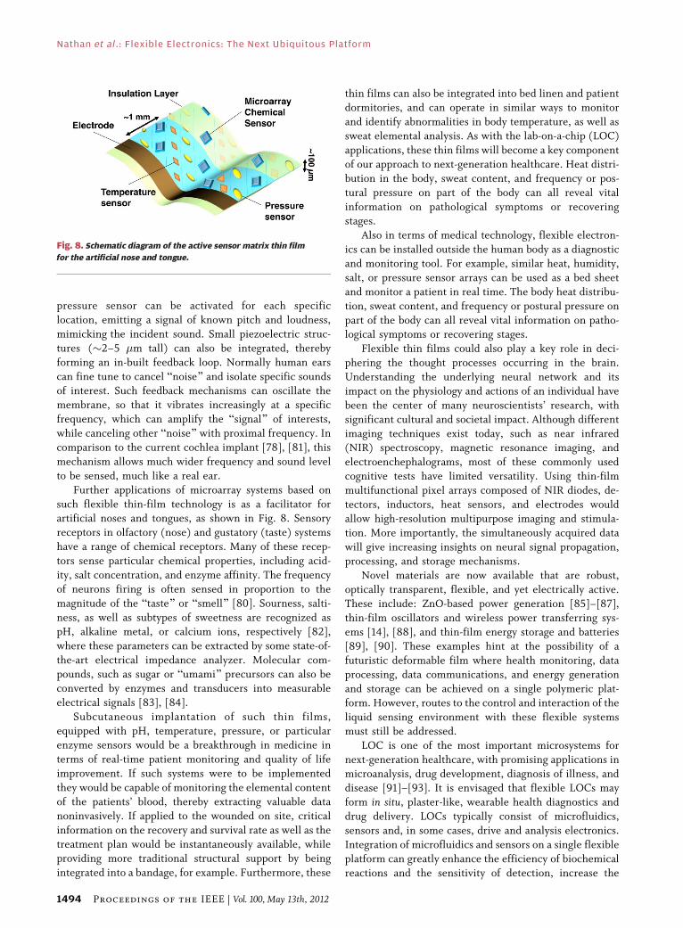
such flexible thin-film technology is as a facilitator forartificial noses and tongues, as shown in Fig. 8. Sensory
receptors in olfactory (nose) and gustatory (taste) systems
have a range of chemical receptors. Many of these recep-
tors sense particular chemical properties, including acid-
ity, salt concentration, and enzyme affinity. The frequency
of neurons firing is often sensed in proportion to the
magnitude of the Btaste[ or Bsmell[ [80]. Sourness, salti-
ness, as well as subtypes of sweetness are recognized aspH, alkaline metal, or calcium ions, respectively [82],
where these parameters can be extracted by some state-of-
the-art electrical impedance analyzer. Molecular com-
pounds, such as sugar or Bumami[ precursors can also be
converted by enzymes and transducers into measurable
electrical signals [83], [84].
Subcutaneous implantation of such thin films,
equipped with pH, temperature, pressure, or particularenzyme sensors would be a breakthrough in medicine in
terms of real-time patient monitoring and quality of life
improvement. If such systems were to be implemented
they would be capable of monitoring the elemental content
of the patients’ blood, thereby extracting valuable data
noninvasively. If applied to the wounded on site, critical
information on the recovery and survival rate as well as the
treatment plan would be instantaneously available, whileproviding more traditional structural support by being
integrated into a bandage, for example. Furthermore, these
thin films can also be integrated into bed linen and patientdormitories, and can operate in similar ways to monitor
and identify abnormalities in body temperature, as well as
sweat elemental analysis. As with the lab-on-a-chip (LOC)
applications, these thin films will become a key component
of our approach to next-generation healthcare. Heat distri-
bution in the body, sweat content, and frequency or pos-
tural pressure on part of the body can all reveal vital
information on pathological symptoms or recoveringstages.
Also in terms of medical technology, flexible electron-
ics can be installed outside the human body as a diagnostic
and monitoring tool. For example, similar heat, humidity,
salt, or pressure sensor arrays can be used as a bed sheet
and monitor a patient in real time. The body heat distribu-
tion, sweat content, and frequency or postural pressure on
part of the body can all reveal vital information on patho-logical symptoms or recovering stages.
Flexible thin films could also play a key role in deci-
phering the thought processes occurring in the brain.
Understanding the underlying neural network and its
impact on the physiology and actions of an individual have
been the center of many neuroscientists’ research, with
significant cultural and societal impact. Although different
imaging techniques exist today, such as near infrared(NIR) spectroscopy, magnetic resonance imaging, and
electroenchephalograms, most of these commonly used
cognitive tests have limited versatility. Using thin-film
multifunctional pixel arrays composed of NIR diodes, de-
tectors, inductors, heat sensors, and electrodes would
allow high-resolution multipurpose imaging and stimula-
tion. More importantly, the simultaneously acquired data
will give increasing insights on neural signal propagation,processing, and storage mechanisms.
Novel materials are now available that are robust,
optically transparent, flexible, and yet electrically active.
These include: ZnO-based power generation [85]–[87],
thin-film oscillators and wireless power transferring sys-
ems [14], [88], and thin-film energy storage and batteries
[89], [90]. These examples hint at the possibility of a
futuristic deformable film where health monitoring, dataprocessing, data communications, and energy generation
and storage can be achieved on a single polymeric plat-
form. However, routes to the control and interaction of the
liquid sensing environment with these flexible systems
must still be addressed.
LOC is one of the most important microsystems for
next-generation healthcare, with promising applications in
microanalysis, drug development, diagnosis of illness, anddisease [91]–[93]. It is envisaged that flexible LOCs may
form in situ, plaster-like, wearable health diagnostics and
drug delivery. LOCs typically consist of microfluidics,
sensors and, in some cases, drive and analysis electronics.
Integration of microfluidics and sensors on a single flexible
platform can greatly enhance the efficiency of biochemical
reactions and the sensitivity of detection, increase the
Fig. 8. Schematic diagram of the active sensor matrix thin film
for the artificial nose and tongue.
Nathan et al.: Flexible Electronics: The Next Ubiquitous Platform
1494 Proceedings of the IEEE | Vol. 100, May 13th, 2012
reaction/detection speed, and reduce the potential crosscontamination, fabrication time, and cost. However, fabri-
cation techniques of microfluidics and sensors are differ-
ent, making the integration of the two main components
complicated, thereby largely increasing the system cost,
particularly on polymer-based substrates.
Micropumps and mixers employing surface acoustic
waves (SAWs) as actuation mechanisms are attractive
alternatives from an integration perspective [94]. Theyoffer great potential for microfluidic applications, as they
are based on low-cost ZnO piezoelectric thin films that can
be deposited on commercially available Si and deformable
substrates. SAW-based micropumps and micromixers are
simple in structure and fabrication, are inexpensive, and
function as active pumping and mixing devices without any
moving parts. They have proven reliable and effective [94].
SAW devices have been reported on nanocrystalline ZnOthin films deposited on Si substrates using RF sputtering
[95]. No direct integration on flexible polymeric substrates
have yet to emerge, though this burgeoning field is certain to
bloom in time following various technological advance-
ments. When an alternating current (ac) signal at the
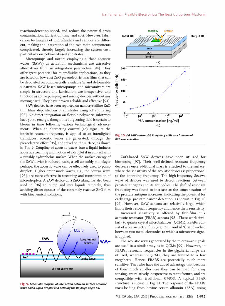
intrinsic resonant frequency is applied to an interdigited
transducer, acoustic waves are generated, through the
piezoelectric effect [95], and travel on the surface, as shownin Fig. 9. Coupling of acoustic waves into a liquid induces
acoustic streaming and motion of a droplet if in contact with
a suitably hydrophobic surface. When the surface energy of
the SAW device is reduced, using a self-assembly monolayer
perhaps, the acoustic wave can be effectively used to pump
droplets. Higher order mode waves, e.g., the Sezawa wave
[96], are more effective in streaming and transportation of
microdroplets. A SAW device on a ZnO island has also beenused in [96] to pump and mix liquids remotely, thus
avoiding direct contact of the extremely reactive ZnO film
with biochemical solutions.
ZnO-based SAW devices have been utilized for
biosensing [97]. Their well-defined resonant frequency
decreases once additional mass is attached to the surface,
where the sensitivity of the acoustic devices is proportional
to the operating frequency. The high-frequency Sezawa
wave of devices was used to detect reactions between
prostate antigens and its antibodies. The shift of resonant
frequency was found to increase as the concentration ofthe prostate antigens increases, indicating the potential for
early stage prostate cancer detection, as shown in Fig. 10
[97]. However, SAW sensors are relatively large, which
limits their resonant frequency and hence their sensitivity.
Increased sensitivity is offered by thin-film bulk
acoustic resonator (FBAR) sensors [98]. These work simi-
larly to quartz crystal microbalances (QCMs). FBARs con-
sist of a piezoelectric film (e.g., ZnO and AlN) sandwichedbetween two metal electrodes to which a microwave signal
is applied.
The acoustic waves generated by the microwave signals
are used in a similar way as in QCMs [99]. However, in
FBARs, resonant frequencies in the gigahertz range are
utilized, whereas in QCMs, they are limited to a few
megahertz. Hence, FBARS are potentially much more
sensitive. They also have the added advantage that becauseof their much smaller size they can be used for array
sensing, are relatively inexpensive to manufacture, and are
compatible with traditional CMOS. A typical FBAR
structure is shown in Fig. 11. The response of the FBARs
mass-loading from bovine serum albumin (BSA), using
Fig. 10. (a) SAW sensor. (b) Frequency shift as a function of
PSA concentration.
Fig. 9. Schematic diagram of interaction between surface acoustic
wave and a liquid droplet and defining the Rayleigh angle (�).
Nathan et al.: Flexible Electronics: The Next Ubiquitous Platform
Vol. 100, May 13th, 2012 | Proceedings of the IEEE 1495

physically adsorbed protein coatings, has been investi-
gated. The response is shown in Fig. 12. For a FBAR
resonating at 1.5 GHZ, a 3 orders of magnitude increase in
response was observed compared with a QCM, for a given
BSA concentration.These results clearly demonstrate the feasibility of
using a single actuation mechanism for both microfluidics
and sensing. They also show the suitability of acoustic
waves for LOC applications. This greatly simplifies the
fabrication and operation of these microsystems, and en-
hances their sensitivity and performance.
Although various technologies have emerged as viable
candidates for biologically compatible electronic interfacesand LOC structures, little has been achieved by way of full-
scale interaction and the next challenge is to fabricate such
structures on deformable plastic substrates. Preliminary
work on this is currently ongoing [100], [101].
V. AUTOMOTIVE INDUSTRY
The combustion reaction has fueled the development of
humanity since the discovery of fire. The main reasons for
the ubiquity of combustion are twofold. The first one
relates to its intrinsic mass and volume energy densities.
For example, 1 kg of crude oil contains nearly 50 MJ ofchemical potential energy. The second one relates to
storage and portability. Crude oil happens to be liquid atsurface conditions, making it easy to store, transport, and
convert, which is fundamental for applications such as
transportation. As a comparison, Li-ion batteries provide
about 0.5 MJ/kg [102]. However, new battery chemistries,
pressure for lower CO2 emissions, and lightweight designs
are contributing toward the electric alternative.
Although electric vehicles trace their invention to the
mid-1800s [103], their widespread adoption has not yetmaterialized. This is partly due to the high energy density
(J/kg) of fossil fuel compared to the batteries [104] with
the implication that electric vehicles require unfeasibly
heavy and large batteries to store equivalent energy as a
tank of fuel. As well as low energy density, batteries suffer
from low power density (W/kg) leading to electric vehicles
with comparatively low performance when compared to
equivalent fuel powered vehicles [105]. Despite theseissues, increasingly scarce fossil fuel resources, as well as
environmental incentives, have increased the adoption of
electric vehicles [106], fueling research and development
in this field.
Advances in thin-film battery technology through the
use of nanostructures for enhanced energy density [107]
and hybrid supercapacitor allowed increased energy and
power densities [108]. Lightweight substrates, such aspolyethylene terephthalate (PET) and paper, have led to a
reduction in battery weight. Furthermore, recent devel-
opments in the structure of batteries [109]–[112] has
resulted in their seamless integration within the carbon-
fiber frames of electric vehicles, leading to significant
overall weight and space savings. Flexible, thin-film
technology is especially beneficial in this instance, as it
allows batteries to be moulded into suitable shapes atrelatively low costs. Fig. 13 shows a schematic of a flexible
thin-film battery on a PET substrate.
Flexible thin-film technology may also find applica-
tions in road signs [113] and markings [114]. Intelligent
roads will be engineered with the aim of improving road
safety, lowering road congestion and energy consumption.
The road and vehicle will be able to interact to dynamically
adjust either party to energetically optimize their systems.The advantage of flexible thin-film technology is its
mechanical durability and ease of inexpensive integration
within the existing road networks.
VI. DISPLAYS AND HUMAN–MACHINEINTERACTIVITY
Improving user experiences with electronic devicesrequires a continuous technological development toward
flexible, deformable architectures, including displays,
processors, memories, and other vital electronic compo-
nents. Such designs will enable wearable, interactive,
portable devices. Possibly the key component here is the
display. Several flexible prototypes have been presented by
different commercial entities over the past few years [115],Fig. 12. Resonant frequency shift as a function of BSA concentration.
Fig. 11. Typical thin-film FBAR structure.
Nathan et al.: Flexible Electronics: The Next Ubiquitous Platform
1496 Proceedings of the IEEE | Vol. 100, May 13th, 2012

[116], most commonly using inkjet printing fabrication of
functional polymer devices with metallic nanoparticle-
based interconnects [116]–[120]. Advancement of print-
able polymers and devices for flexible architectures has
also been explored using other nanostructures, such as
NWs [121], CNTs [45], [122], and graphene [46].
The advent of touchscreen-enabled devices means fur-
ther improvement in user-device interaction. An impor-tant aspect in the overall user experience now primarily
revolves around the display itself. In this context, nonvi-
sual interaction with displayed information is a vital
element for next-generation display-centric devices. These
are necessarily heading toward flexible form factors. New
interaction technologies for touchscreens are continuously
being developed and commercialized, for example, multi-
touch gestures [123], [124]. However, these still fail toprovide 100% satisfaction in terms of user experience,
since they only give real-time visual feedback, requiring
significant cognitive efforts. Current solutions for lower
cognitive effort touch interfaces, in particular, vibration-
enabled feedback, generate simple, monolithic vibrations
(through vibramotors [125], [126], impact actuators [127],
[128], or piezo-based [129] feedback systems) over the
entire device, without conveying explicit interactioninformation to the user. In this context, flexible displays
with location-specific, real-time textural feedback thatmimic the display itself can truly revolutionize the user
interface ecosystem.
There have been several attempts at location-specific
perception for general purpose electronic devices, most
notably, using an array of electrodes through electro-
cutaneous stimulation (i.e., passing a small current from
electrodes to the afferent nerve fibers in the user’s finger
to generate perceptive stimulation [130], [131]). However,such an architecture is incompatible with the current
generation of display-centric devices, which inherently
dictates that the feedback must come from the display
surface itself without visually obstructing it [129].
One simple way to achieve haptic feedback without
obscuring the display itself is to use Belectrovibration,[ a
phenomenon reported over 50 years ago [132], [133]. This
was described as Bproducing a characteristic feeling whena metal, connected to an ac power line and covered by a
thin insulator, is touched, which disappears when the
power line is disconnected[ [133]. This has later been
explained through electrostatic interaction between touch
surface and finger [134]. As users slide their fingers on the
surface, the applied time-varying potential induces
intermittent attractive and repulsive electrostatic forces
between the buried conducting layer and the finger. Thiselectrostatic attraction varies the normal contact force
between user’s skin and surface and, in turn, modulates
the dynamic friction and touch perception [132], [135].
Subsequent studies indicate correlations between the na-
ture of the applied electrical signal to the buried
conductor and the touch perception, promising a reason-
ably realistic programmable touch surface [134], [135].
Flexibility of such devices is strongly limited by conven-tional transparent conductors (TC), dominated by brittle
metal–oxide–semiconductors [135], [136]. Graphene,
being the ideal flexible TC, coated with a flexible polymer
dielectric layer, such as parylene [137], can be used to
fabricate fully transparent, location-specific feedback
surfaces [52]. Such a device needs to be visually transparent
so that it can be unobtrusively laid over existing flexible
displays, enabling the generation of the location-specific,real-time programmable textures. A graphene-based pro-
grammable touch surface with flexible device architecture
was recently demonstrated [138]. A generalized device
schematic is shown in Fig. 14. It consists of a graphene-
based TC integrated on a flexible display, a flexible,
optically transparent polymer dielectric layer coated with a
nanostructured touch surface. This prototype flexible
electrotactile device accepts input signal patterns storedin audio files from a mobile phone, can operate with a wide
range of applied electrical signals, and is capable of
generating varying touch perceptions [138]. When inte-
grated onto touchscreens, this could provide a completely
new interaction experience for general users, as well as
becoming one of the most essential communication media
for the visually impaired.
Fig. 13. (a) Battery structure. Each component must withstand
flexing in order to get an overall flexible battery. (b) Optical
micrograph of a flexible battery during flexing.
Nathan et al.: Flexible Electronics: The Next Ubiquitous Platform
Vol. 100, May 13th, 2012 | Proceedings of the IEEE 1497
VII. ENERGY MANAGEMENT ANDMOBILE DEVICES
A large demand for portable, on-demand energy comes
from consumer electronic devices like RFIDs, mobile
phones, laptops, netbooks, tablets, and portable music
players. In these situations, batteries, and more recently,electrochemical capacitors, have been the sole solution.
Many advances have been made in battery technology in
recent years, with research primarily directed in two
streams. One aimed at: increasing energy and power
densities via new chemistry; new materials or by the
optimization of current systems; reducing the ratio of
inactive to active components to improve energy
density; increasing conversion efficiency and rechargeability; as well as enhancing safety and environmental
characteristics. In particular,
• Nanomaterials play a big role in this development.
The fine level of structural control they allow (e.g.,
higher surface area, direct electron transport, hy-
brid materials, and granular control of architec-
ture) opens up possibilities for a greater control of
charge transport and surface phenomena at theelectrode interfaces. These developments have also
allowed the use of materials and chemistries
previously discarded, such as Si anodes [139] and
Li-air batteries [140], paving the way for further
enhanced energy and power densities. Some of the
benefits include high surface areas with controlled
porous structure for optimum ion penetration,
permitting faster charge/discharge capabilities[141]. Fabrication of hybrid materials combines
high conductivity and high storage capacity in an
architectured fashion [142].
• Use of entangled nanomaterials, which tolerate
mechanical flexure without surface-occluding bin-
ders [143]. Nanomaterials, such as SiNWs, which
make use of higher surface areas, but also allow
mechanical tolerance for materials previously not
considered practical due to volume expansion andcracking [139].
• Prevention of polymer crystallization, to improve
the ionic conductivity of polymer or ionic-liquid-
based electrolytes provide greater mechanical ri-
gidity and higher voltage tolerance [144].
On the other hand, much emphasis is placed on de-
signing alternative form factors, departing from the solid
bulk component toward thin, flexible [145], and evenstretchable [146] and transparent [143] devices.
The advent of nanotechnology is boosting the devel-
opment of energy conversion and storage. For example,
graphene has already been exploited for a variety of energy
applications such as batteries [147], [148], supercapacitors
[149]–[152], water splitting [153], and PVs [154]. The large
accessible surface-area-to-volume ratio of graphene makes
it very attractive for such devices due to their high stabilityin electrochemical environments [149], mechanical flex-
ibility [155], excellent electronic [40], and optical
properties [52].
Although the use of graphene in energy applications
has just started, the results up to date are promising. For
instance, graphene-based supercapacitors outperform
those based on activated carbon, with energy densities
comparable with commercially available batteries [151].Moreover, graphene could be used for a new genera-
tion of energy harvesting nanodevices, such as nanooptoe-
lectromechanical systems (NOEMS). These could access
energy sources arising at the nanoscale, converting energy
from environmental sources, such as ambient noise or
electromagnetic radiation, to mechanical vibrations.
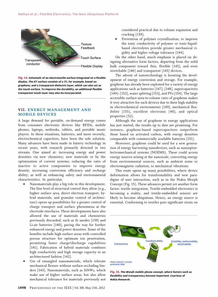
This route opens up many possibilities, where device
deformation allows for transformability and new para-digms of user interaction, such as in the Nokia Morph
Concept (Fig. 15). These advances permit yet another form
factor: textile integration. Textile-embedded electronics is
becoming a reality, and textile-embedded sensors are
likely to become ubiquitous. Hence, an energy source is
essential. Conforming to textiles puts significant strain on
Fig. 14. Schematic of an electrotactile surface integrated on a flexible
display. The ET surface consists of a TC, for example, based on
graphene, and a transparent dielectric layer, which can also act as
the touch surface. To improve the durability, an additional flexible
transparent touch layer may also be incorporated.
Fig. 15. The Morph mobile phone concept, where factors such as
flexibility and transparency become important. Courtesy of
Nokia Research.
Nathan et al.: Flexible Electronics: The Next Ubiquitous Platform
1498 Proceedings of the IEEE | Vol. 100, May 13th, 2012
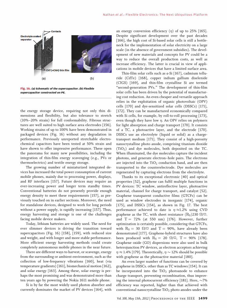
the energy storage device, requiring not only thin di-
mensions and flexibility, but also tolerance to stretch
(10%–20% strain) for full conformability. Fibrous struc-
tures are well suited to high surface area electrodes [156].
Working strains of up to 100% have been demonstrated in
packaged devices (Fig. 16) without any degradation inperformance. Previously unreported stretchable electro-
chemical capacitors have been tested at 50% strain and
have shown to offer impressive performance. These open
the panorama for many new possibilities, including the
integration of thin-film energy scavenging (e.g., PVs or
thermoelectrics) and textile energy storage.
The growing number of miniaturized integrated de-
vices has increased the total power consumption of currentmobile phones, mainly due to processing power, displays,
and RF interfaces [157]. Future devices may require an
ever-increasing power and longer term standby times.
Conventional batteries do not presently provide enough
energy density to meet these requirements [157], as pre-
viously touched on in earlier sections. Moreover, the need
for standalone devices, designed to work for long periods
without a power supply, is rapidly increasing [157]. Thus,energy harvesting and storage is one of the challenges
facing mobile device makers.
Today, lithium batteries are widely used. The need for
ever slimmer devices is driving the transition toward
supercapacitors (Fig. 16) [158], [159], with reduced size
and weight, and with longer and more stable performance.
More efficient energy harvesting methods could create
completely autonomous mobile phones in the near future.There are different ways to harvest, or scavenge, energy
from the surrounding or ambient environment, such as the
collection of low-frequency vibrations [160], heat (via
temperature gradients) [161], biomechanical motion [162],
and solar energy [163]. Among these, solar energy is per-
haps the most promising and was demonstrated more than
ten years ago by powering the Nokia 1611 mobile phone.
Si is by far the most widely used photon absorber andcurrently dominates the market of PV devices [164], with
an energy conversion efficiency ð�Þ of up to 25% [165].Despite significant development over the past decades
[166], the high cost of Si-based solar cells is still a bottle-
neck for the implementation of solar electricity on a large
scale (in the absence of government subsidies). The devel-
opment of new materials and concepts for PV could be a
way to reduce the overall production costs, as well as
increase efficiency. The latter is crucial in view of appli-
cations in mobile devices that have a limited surface area.Thin-film solar cells such as a-Si [167], cadmium tellu-
ride (CdTe) [168], copper indium gallium diselenide
(CIGS) [169], and thin-film crystalline Si are termed
Bsecond-generation PVs.[ The development of thin-film
solar cells has been driven by the potential of manufactur-
ing cost reduction. An even cheaper and versatile approach
relies in the exploitation of organic photovoltaic (OPV)
cells [170] and dye-sensitized solar cells (DSSCs) [171],[172]. They can be manufactured economically compared
with Si cells, for example, by roll-to-roll processing [173],
even though they have low �. An OPV relies on polymers
for light absorption and charge transport [170]. It consists
of a TC, a photoactive layer, and the electrode [170].
DSSCs use an electrolyte (liquid or solid) as a charge-
transport medium [171]. They consist of a high-porosity
nanocrystalline photo anode, comprising titanium dioxide(TiO2) and dye molecules, both deposited on the TC.
When illuminated, the dye molecules capture the incident
photons, and generate electron–hole pairs. The electrons
are injected into the TiO2 conduction band, and are then
transported to the counterelectrode. Dye molecules are
regenerated by capturing electrons from the electrolyte.
Thanks to its exceptional electronic [40] and optical
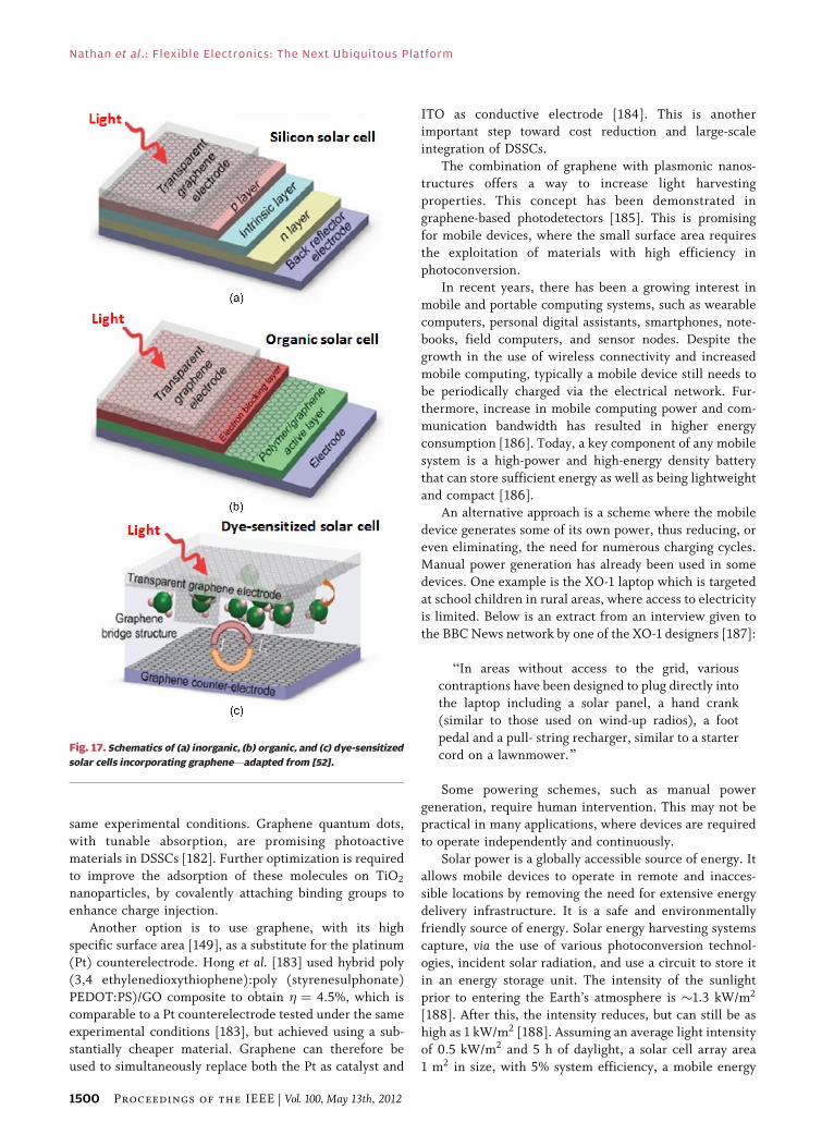
properties [52], graphene can fulfil multiple functions inPV devices: TC window, antireflective layer, photoactive
material, channel for charge transport, and catalyst [52].
Graphene transparent conductive films (GTCFs) can be
used as window electrodes in inorganic [174], organic
[175], and DSSCs [154], as shown in Fig. 17. The best
performance achieved to date is � �1.2% using CVD
graphene as the TC, with sheet resistance ðRSÞ230 �/Ì.
and T ¼ 72% (at 550 nm) [176]. However, furtheroptimization is certainly possible, considering that GTCFs,
with RS ¼ 30 �/Ì and T ¼ 90%, have already been
demonstrated [177]. Graphene-hybrid structures have also
been produced with RS ¼ 20 �/Ì, T ¼ 90% [178].
Graphene oxide (GO) dispersions were also used in bulk
heterojunction PV devices, as electron acceptors achieving
� � 1.4% [179]. Theoretically, � � 12% should be possible
with graphene as the photoactive material [180].An even larger number of functions can be covered by
graphene in DSSCs. other than as TC windows [154]. It can
be incorporated into the TiO2 photoanode to enhance
charge transport, preventing recombination, thus improv-
ing the internal photocurrent efficiency [181]. Here, �7%
efficiency was reported, higher than that achieved with
conventional nanocrystalline TiO2 photo anodes under the
Fig. 16. (a) Schematic of the supercapacitor. (b) Flexible
supercapacitor constructed on PE.
Nathan et al.: Flexible Electronics: The Next Ubiquitous Platform
Vol. 100, May 13th, 2012 | Proceedings of the IEEE 1499
same experimental conditions. Graphene quantum dots,
with tunable absorption, are promising photoactive
materials in DSSCs [182]. Further optimization is requiredto improve the adsorption of these molecules on TiO2
nanoparticles, by covalently attaching binding groups to
enhance charge injection.
Another option is to use graphene, with its high
specific surface area [149], as a substitute for the platinum
(Pt) counterelectrode. Hong et al. [183] used hybrid poly
(3,4 ethylenedioxythiophene):poly (styrenesulphonate)
PEDOT:PS)/GO composite to obtain � ¼ 4.5%, which iscomparable to a Pt counterelectrode tested under the same
experimental conditions [183], but achieved using a sub-
stantially cheaper material. Graphene can therefore be
used to simultaneously replace both the Pt as catalyst and
ITO as conductive electrode [184]. This is anotherimportant step toward cost reduction and large-scale
integration of DSSCs.
The combination of graphene with plasmonic nanos-
tructures offers a way to increase light harvesting
properties. This concept has been demonstrated in
graphene-based photodetectors [185]. This is promising
for mobile devices, where the small surface area requires
the exploitation of materials with high efficiency inphotoconversion.
In recent years, there has been a growing interest in
mobile and portable computing systems, such as wearable
computers, personal digital assistants, smartphones, note-
books, field computers, and sensor nodes. Despite the
growth in the use of wireless connectivity and increased
mobile computing, typically a mobile device still needs to
be periodically charged via the electrical network. Fur-thermore, increase in mobile computing power and com-
munication bandwidth has resulted in higher energy
consumption [186]. Today, a key component of any mobile
system is a high-power and high-energy density battery
that can store sufficient energy as well as being lightweight
and compact [186].
An alternative approach is a scheme where the mobile
device generates some of its own power, thus reducing, oreven eliminating, the need for numerous charging cycles.
Manual power generation has already been used in some
devices. One example is the XO-1 laptop which is targeted
at school children in rural areas, where access to electricity
is limited. Below is an extract from an interview given to
the BBC News network by one of the XO-1 designers [187]:
BIn areas without access to the grid, variouscontraptions have been designed to plug directly into
the laptop including a solar panel, a hand crank
(similar to those used on wind-up radios), a foot
pedal and a pull- string recharger, similar to a starter
cord on a lawnmower.[
Some powering schemes, such as manual power
generation, require human intervention. This may not bepractical in many applications, where devices are required
to operate independently and continuously.
Solar power is a globally accessible source of energy. It
allows mobile devices to operate in remote and inacces-
sible locations by removing the need for extensive energy
delivery infrastructure. It is a safe and environmentally
friendly source of energy. Solar energy harvesting systems
capture, via the use of various photoconversion technol-ogies, incident solar radiation, and use a circuit to store it
in an energy storage unit. The intensity of the sunlight
prior to entering the Earth’s atmosphere is �1.3 kW/m2
[188]. After this, the intensity reduces, but can still be as
high as 1 kW/m2 [188]. Assuming an average light intensity
of 0:5 kW/m2 and 5 h of daylight, a solar cell array area
1 m2 in size, with 5% system efficiency, a mobile energy
Fig. 17. Schematics of (a) inorganic, (b) organic, and (c) dye-sensitized
solar cells incorporating grapheneVadapted from [52].
Nathan et al.: Flexible Electronics: The Next Ubiquitous Platform
1500 Proceedings of the IEEE | Vol. 100, May 13th, 2012
harvesting system could generate and store 125 Wh/day. Atypical Li-ion battery cell used in modern laptops can store
60 Wh. Therefore, this estimate suggests that an energy
harvesting system such as this can produce over twice the
amount of the energy stored in a laptop battery in one day.
Such a high level of energy, combined with a suitable
power management system, has a potential to be a viable
energy source for a range of remote devices.
A mobile solar energy harvesting system [189] requiresa number of attributes to allow integration with mobile
devices. It should be lightweight and durable. Mechani-
cally flexible systems would improve durability and allow
enhanced integration. A candidate for such a system is a
thin-film system fabricated on flexible substrates. Thin-
film-based solar cells can achieve higher power per unit
mass compared with bulk solar cells (such as c-Si). For
example, power density achieved from thin-film cells is inthe range of 40 W/kg for triple-junction a-Si solar cells on
plastic substrate. Fig. 18 shows a possible integration route
for mobile energy systems, with a display unit, with the
aim of harvesting ambient illumination or some of the
optical losses within organic light emitting diode displays
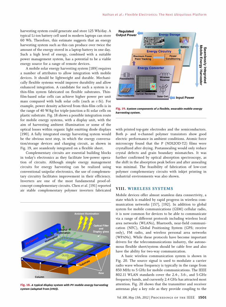
[190]. A fully integrated energy harvesting system would
be the obvious next step, in which the energy conversa-
tion/storage devices and charging circuit, as shown inFig. 19, are seamlessly integrated on a flexible sheet.
Complementary circuits are essential building blocks
in today’s electronics as they facilitate low-power opera-
tion of circuits. Although simple energy management
circuits for energy harvesting can be realized using
conventional unipolar electronics, the use of complemen-
tary circuitry facilitates improvement in their efficiency.
Inverters are one of the most fundamental proof-of-concept complementary circuits. Chen et al. [191] reported
air stable complementary polymer inverters fabricated
with printed top-gate electrodes and the semiconductors.
Both p- and n-channel polymer transistors show good
electric performance in ambient conditions. Atomic force
microscopy found that the P (NDI2OD-T2) films were
crystallized after drying. Postannealing would only reduce
crystal defects and grain boundary mismatches. It wasfurther confirmed by optical absorption spectroscopy, as
the shift in the absorption peak before and after annealing
was minimal. The feasibility of fabrication of low-cost
polymer complementary circuits with inkjet printing in
industrial environments was also shown.
VIII . WIRELESS SYSTEMS
Mobile devices offer almost seamless data connectivity, a
state which is enabled by rapid progress in wireless com-
munication networks [157], [192]. In addition to global
system for mobile communications (GSM) cellular radio,
it is now common for devices to be able to communicate
via a range of different protocols including wireless localarea networks (WLANs), Bluetooth, near-field communi-
cation (NFC), Global Positioning System (GPS; receive
only), FM radio, and wireless personal area networks
(WPANs). While these protocols have become important
drivers for the telecommunications industry, the autono-
mous flexible sheet/system should be cable free and also
have the ability for two-way communication.
A basic wireless communication system is shown inFig. 20. The source signal is used to modulate a carrier
radio wave whose frequency is typically in the range from
850 MHz to 5 GHz for mobile communications. The IEEE
802.11 WLAN standards cover the 2.4-, 3.6-, and 5-GHz
frequency bands, and currently 2.4 GHz has attracted most
attention. Fig. 20 shows that the transmitter and receiver
antennas play a key role as they provide coupling to the
Fig. 19. System components of a flexible, wearable mobile energy
harvesting system.
Fig. 18. A typical display system with PV mobile energy harvesting
system (adapted from [190]).
Nathan et al.: Flexible Electronics: The Next Ubiquitous Platform
Vol. 100, May 13th, 2012 | Proceedings of the IEEE 1501
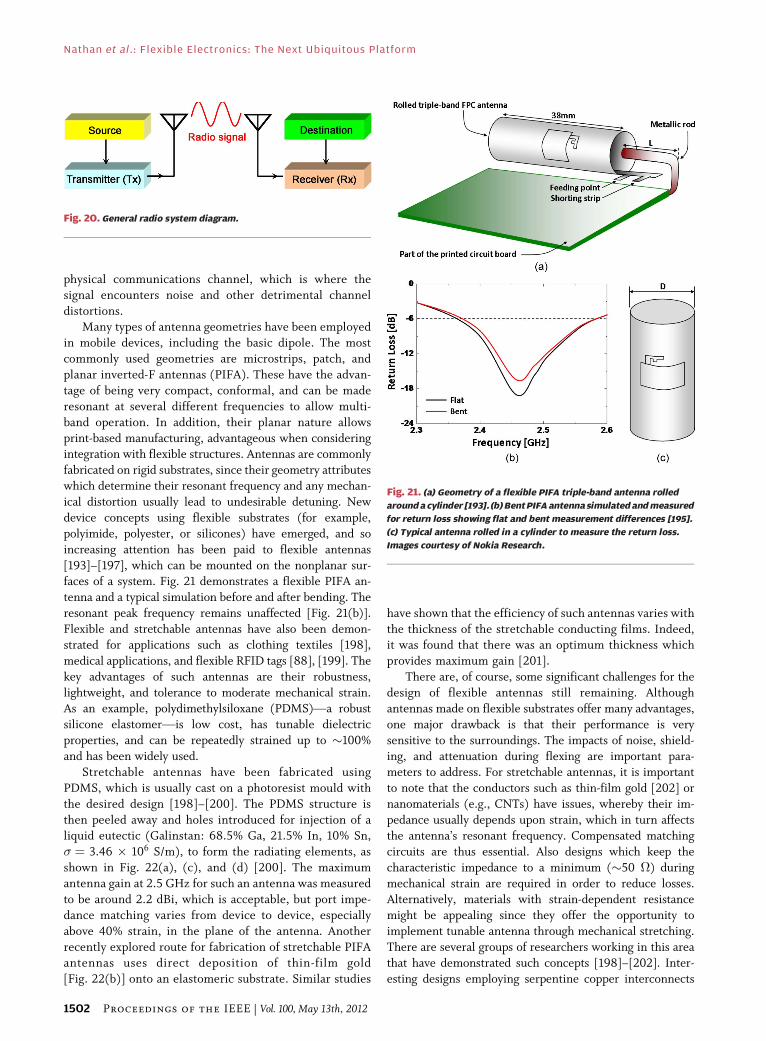
physical communications channel, which is where the
signal encounters noise and other detrimental channel
distortions.Many types of antenna geometries have been employed
in mobile devices, including the basic dipole. The most
commonly used geometries are microstrips, patch, and
planar inverted-F antennas (PIFA). These have the advan-
tage of being very compact, conformal, and can be made
resonant at several different frequencies to allow multi-
band operation. In addition, their planar nature allows
print-based manufacturing, advantageous when consideringintegration with flexible structures. Antennas are commonly
fabricated on rigid substrates, since their geometry attributes
which determine their resonant frequency and any mechan-
ical distortion usually lead to undesirable detuning. New
device concepts using flexible substrates (for example,
polyimide, polyester, or silicones) have emerged, and so
increasing attention has been paid to flexible antennas
[193]–[197], which can be mounted on the nonplanar sur-faces of a system. Fig. 21 demonstrates a flexible PIFA an-
tenna and a typical simulation before and after bending. The
resonant peak frequency remains unaffected [Fig. 21(b)].
Flexible and stretchable antennas have also been demon-
strated for applications such as clothing textiles [198],
medical applications, and flexible RFID tags [88], [199]. The
key advantages of such antennas are their robustness,
lightweight, and tolerance to moderate mechanical strain.As an example, polydimethylsiloxane (PDMS)Va robust
silicone elastomerVis low cost, has tunable dielectric
properties, and can be repeatedly strained up to �100%
and has been widely used.
Stretchable antennas have been fabricated using
PDMS, which is usually cast on a photoresist mould with
the desired design [198]–[200]. The PDMS structure is
then peeled away and holes introduced for injection of aliquid eutectic (Galinstan: 68.5% Ga, 21.5% In, 10% Sn,
� ¼ 3.46 � 106 S/m), to form the radiating elements, as
shown in Fig. 22(a), (c), and (d) [200]. The maximum
antenna gain at 2.5 GHz for such an antenna was measured
to be around 2.2 dBi, which is acceptable, but port impe-
dance matching varies from device to device, especially
above 40% strain, in the plane of the antenna. Another
recently explored route for fabrication of stretchable PIFAantennas uses direct deposition of thin-film gold
[Fig. 22(b)] onto an elastomeric substrate. Similar studies
have shown that the efficiency of such antennas varies with
the thickness of the stretchable conducting films. Indeed,it was found that there was an optimum thickness which
provides maximum gain [201].
There are, of course, some significant challenges for the
design of flexible antennas still remaining. Although
antennas made on flexible substrates offer many advantages,
one major drawback is that their performance is very
sensitive to the surroundings. The impacts of noise, shield-
ing, and attenuation during flexing are important para-meters to address. For stretchable antennas, it is important
to note that the conductors such as thin-film gold [202] or
nanomaterials (e.g., CNTs) have issues, whereby their im-
pedance usually depends upon strain, which in turn affects
the antenna’s resonant frequency. Compensated matching
circuits are thus essential. Also designs which keep the
characteristic impedance to a minimum (�50 �) during
mechanical strain are required in order to reduce losses.Alternatively, materials with strain-dependent resistance
might be appealing since they offer the opportunity to
implement tunable antenna through mechanical stretching.
There are several groups of researchers working in this area
that have demonstrated such concepts [198]–[202]. Inter-
esting designs employing serpentine copper interconnects
Fig. 21. (a) Geometry of a flexible PIFA triple-band antenna rolled
aroundacylinder [193]. (b)BentPIFAantennasimulatedandmeasured
for return loss showing flat and bent measurement differences [195].
(c) Typical antenna rolled in a cylinder to measure the return loss.
Images courtesy of Nokia Research.
Fig. 20. General radio system diagram.
Nathan et al.: Flexible Electronics: The Next Ubiquitous Platform
1502 Proceedings of the IEEE | Vol. 100, May 13th, 2012
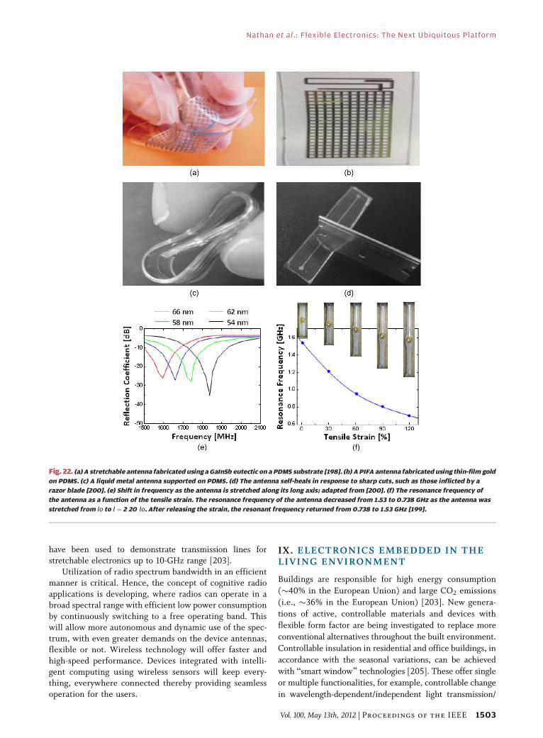
have been used to demonstrate transmission lines forstretchable electronics up to 10-GHz range [203].
Utilization of radio spectrum bandwidth in an efficientmanner is critical. Hence, the concept of cognitive radioapplications is developing, where radios can operate in abroad spectral range with efficient low power consumptionby continuously switching to a free operating band. Thiswill allow more autonomous and dynamic use of the spec-trum, with even greater demands on the device antennas,flexible or not. Wireless technology will offer faster andhigh-speed performance. Devices integrated with intelli-gent computing using wireless sensors will keep every-thing, everywhere connected thereby providing seamlessoperation for the users.
IX. ELECTRONICS EMBEDDED IN THELIVING ENVIRONMENT
Buildings are responsible for high energy consumption
(�40% in the European Union) and large CO2 emissions
(i.e., �36% in the European Union) [203]. New genera-
tions of active, controllable materials and devices with
flexible form factor are being investigated to replace more
conventional alternatives throughout the built environment.
Controllable insulation in residential and office buildings, in
accordance with the seasonal variations, can be achieved
with Bsmart window[ technologies [205]. These offer single
or multiple functionalities, for example, controllable change
in wavelength-dependent/independent light transmission/
Fig. 22. (a)A stretchable antenna fabricatedusing aGaInSb eutectic onaPDMS substrate [198]. (b) APIFA antenna fabricatedusing thin-filmgold
on PDMS. (c) A liquid metal antenna supported on PDMS. (d) The antenna self-heals in response to sharp cuts, such as those inflicted by a
razor blade [200]. (e) Shift in frequency as the antenna is stretched along its long axis; adapted from [200]. (f) The resonance frequency of
the antenna as a function of the tensile strain. The resonance frequency of the antenna decreased from 1.53 to 0.738 GHz as the antenna was
stretched from lo to l ¼ 2:20 lo. After releasing the strain, the resonant frequency returned from 0.738 to 1.53 GHz [199].
Nathan et al.: Flexible Electronics: The Next Ubiquitous Platform
Vol. 100, May 13th, 2012 | Proceedings of the IEEE 1503
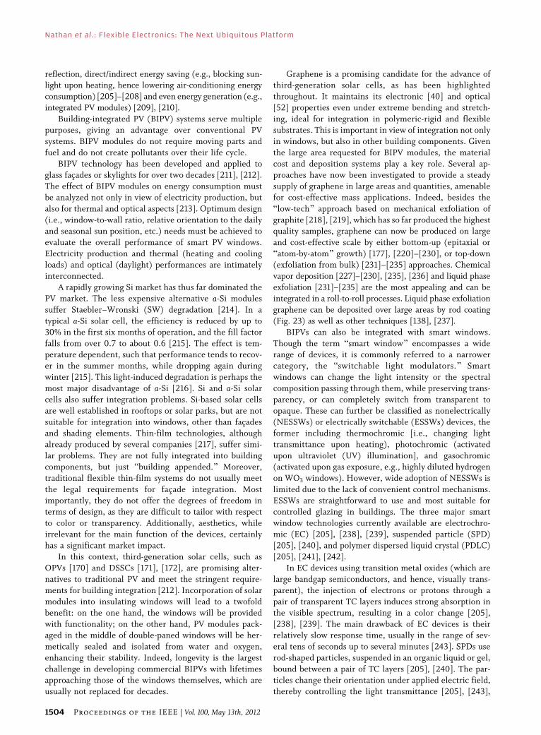
reflection, direct/indirect energy saving (e.g., blocking sun-light upon heating, hence lowering air-conditioning energy
consumption) [205]–[208] and even energy generation (e.g.,
integrated PV modules) [209], [210].
Building-integrated PV (BIPV) systems serve multiple
purposes, giving an advantage over conventional PV
systems. BIPV modules do not require moving parts and
fuel and do not create pollutants over their life cycle.
BIPV technology has been developed and applied toglass facades or skylights for over two decades [211], [212].
The effect of BIPV modules on energy consumption must
be analyzed not only in view of electricity production, but
also for thermal and optical aspects [213]. Optimum design
(i.e., window-to-wall ratio, relative orientation to the daily
and seasonal sun position, etc.) needs must be achieved to
evaluate the overall performance of smart PV windows.
Electricity production and thermal (heating and coolingloads) and optical (daylight) performances are intimately
interconnected.
A rapidly growing Si market has thus far dominated the
PV market. The less expensive alternative a-Si modules
suffer Staebler–Wronski (SW) degradation [214]. In a
typical a-Si solar cell, the efficiency is reduced by up to
30% in the first six months of operation, and the fill factor
falls from over 0.7 to about 0.6 [215]. The effect is tem-perature dependent, such that performance tends to recov-
er in the summer months, while dropping again during
winter [215]. This light-induced degradation is perhaps the
most major disadvantage of a-Si [216]. Si and a-Si solar
cells also suffer integration problems. Si-based solar cells
are well established in rooftops or solar parks, but are not
suitable for integration into windows, other than facades
and shading elements. Thin-film technologies, althoughalready produced by several companies [217], suffer simi-
lar problems. They are not fully integrated into building
components, but just Bbuilding appended.[ Moreover,
traditional flexible thin-film systems do not usually meet
the legal requirements for facade integration. Most
importantly, they do not offer the degrees of freedom in
terms of design, as they are difficult to tailor with respect
to color or transparency. Additionally, aesthetics, whileirrelevant for the main function of the devices, certainly
has a significant market impact.
In this context, third-generation solar cells, such as
OPVs [170] and DSSCs [171], [172], are promising alter-
natives to traditional PV and meet the stringent require-
ments for building integration [212]. Incorporation of solar
modules into insulating windows will lead to a twofold
benefit: on the one hand, the windows will be providedwith functionality; on the other hand, PV modules pack-
aged in the middle of double-paned windows will be her-
metically sealed and isolated from water and oxygen,
enhancing their stability. Indeed, longevity is the largest
challenge in developing commercial BIPVs with lifetimes
approaching those of the windows themselves, which are
usually not replaced for decades.
Graphene is a promising candidate for the advance ofthird-generation solar cells, as has been highlighted
throughout. It maintains its electronic [40] and optical
[52] properties even under extreme bending and stretch-
ing, ideal for integration in polymeric-rigid and flexible
substrates. This is important in view of integration not only
in windows, but also in other building components. Given
the large area requested for BIPV modules, the material
cost and deposition systems play a key role. Several ap-proaches have now been investigated to provide a steady
supply of graphene in large areas and quantities, amenable
for cost-effective mass applications. Indeed, besides the
Blow-tech[ approach based on mechanical exfoliation of
graphite [218], [219], which has so far produced the highest
quality samples, graphene can now be produced on large
and cost-effective scale by either bottom-up (epitaxial or
Batom-by-atom[ growth) [177], [220]–[230], or top-down(exfoliation from bulk) [231]–[235] approaches. Chemical
vapor deposition [227]–[230], [235], [236] and liquid phase
exfoliation [231]–[235] are the most appealing and can be
integrated in a roll-to-roll processes. Liquid phase exfoliation
graphene can be deposited over large areas by rod coating
(Fig. 23) as well as other techniques [138], [237].
BIPVs can also be integrated with smart windows.
Though the term Bsmart window[ encompasses a widerange of devices, it is commonly referred to a narrower
category, the Bswitchable light modulators.[ Smart
windows can change the light intensity or the spectral
composition passing through them, while preserving trans-
parency, or can completely switch from transparent to
opaque. These can further be classified as nonelectrically
(NESSWs) or electrically switchable (ESSWs) devices, the
former including thermochromic [i.e., changing lighttransmittance upon heating), photochromic (activated
upon ultraviolet (UV) illumination], and gasochromic
(activated upon gas exposure, e.g., highly diluted hydrogen
on WO3 windows). However, wide adoption of NESSWs is
limited due to the lack of convenient control mechanisms.
ESSWs are straightforward to use and most suitable for
controlled glazing in buildings. The three major smart
window technologies currently available are electrochro-mic (EC) [205], [238], [239], suspended particle (SPD)
[205], [240], and polymer dispersed liquid crystal (PDLC)
[205], [241], [242].
In EC devices using transition metal oxides (which are
large bandgap semiconductors, and hence, visually trans-
parent), the injection of electrons or protons through a
pair of transparent TC layers induces strong absorption in
the visible spectrum, resulting in a color change [205],[238], [239]. The main drawback of EC devices is their
relatively slow response time, usually in the range of sev-
eral tens of seconds up to several minutes [243]. SPDs use
rod-shaped particles, suspended in an organic liquid or gel,
bound between a pair of TC layers [205], [240]. The par-
ticles change their orientation under applied electric field,
thereby controlling the light transmittance [205], [243],
Nathan et al.: Flexible Electronics: The Next Ubiquitous Platform
1504 Proceedings of the IEEE | Vol. 100, May 13th, 2012
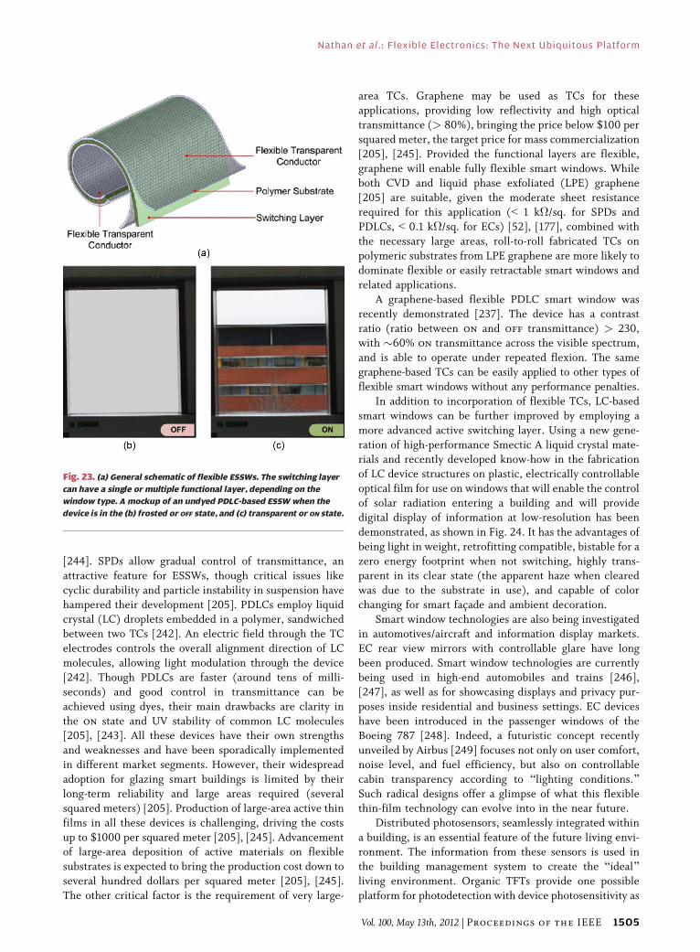
[244]. SPDs allow gradual control of transmittance, an
attractive feature for ESSWs, though critical issues like
cyclic durability and particle instability in suspension have
hampered their development [205]. PDLCs employ liquidcrystal (LC) droplets embedded in a polymer, sandwiched
between two TCs [242]. An electric field through the TC
electrodes controls the overall alignment direction of LC
molecules, allowing light modulation through the device
[242]. Though PDLCs are faster (around tens of milli-
seconds) and good control in transmittance can be
achieved using dyes, their main drawbacks are clarity in
the on state and UV stability of common LC molecules[205], [243]. All these devices have their own strengths
and weaknesses and have been sporadically implemented
in different market segments. However, their widespread
adoption for glazing smart buildings is limited by their
long-term reliability and large areas required (several
squared meters) [205]. Production of large-area active thin
films in all these devices is challenging, driving the costs
up to $1000 per squared meter [205], [245]. Advancementof large-area deposition of active materials on flexible
substrates is expected to bring the production cost down to
several hundred dollars per squared meter [205], [245].
The other critical factor is the requirement of very large-
area TCs. Graphene may be used as TCs for theseapplications, providing low reflectivity and high optical
transmittance (> 80%), bringing the price below $100 per
squared meter, the target price for mass commercialization
[205], [245]. Provided the functional layers are flexible,
graphene will enable fully flexible smart windows. While
both CVD and liquid phase exfoliated (LPE) graphene
[205] are suitable, given the moderate sheet resistance
required for this application (G 1 k�/sq. for SPDs andPDLCs, G 0.1 k�/sq. for ECs) [52], [177], combined with
the necessary large areas, roll-to-roll fabricated TCs on
polymeric substrates from LPE graphene are more likely to
dominate flexible or easily retractable smart windows and
related applications.
A graphene-based flexible PDLC smart window was
recently demonstrated [237]. The device has a contrast
ratio (ratio between on and off transmittance) > 230,with �60% on transmittance across the visible spectrum,
and is able to operate under repeated flexion. The same
graphene-based TCs can be easily applied to other types of
flexible smart windows without any performance penalties.
In addition to incorporation of flexible TCs, LC-based
smart windows can be further improved by employing a
more advanced active switching layer. Using a new gene-
ration of high-performance Smectic A liquid crystal mate-rials and recently developed know-how in the fabrication
of LC device structures on plastic, electrically controllable
optical film for use on windows that will enable the control
of solar radiation entering a building and will provide
digital display of information at low-resolution has been
demonstrated, as shown in Fig. 24. It has the advantages of
being light in weight, retrofitting compatible, bistable for a
zero energy footprint when not switching, highly trans-parent in its clear state (the apparent haze when cleared
was due to the substrate in use), and capable of color
changing for smart facade and ambient decoration.
Smart window technologies are also being investigated
in automotives/aircraft and information display markets.
EC rear view mirrors with controllable glare have long
been produced. Smart window technologies are currently
being used in high-end automobiles and trains [246],[247], as well as for showcasing displays and privacy pur-
poses inside residential and business settings. EC devices
have been introduced in the passenger windows of the
Boeing 787 [248]. Indeed, a futuristic concept recently
unveiled by Airbus [249] focuses not only on user comfort,
noise level, and fuel efficiency, but also on controllable
cabin transparency according to Blighting conditions.[Such radical designs offer a glimpse of what this flexiblethin-film technology can evolve into in the near future.
Distributed photosensors, seamlessly integrated within
a building, is an essential feature of the future living envi-
ronment. The information from these sensors is used in
the building management system to create the Bideal[living environment. Organic TFTs provide one possible
platform for photodetection with device photosensitivity as
Fig. 23. (a) General schematic of flexible ESSWs. The switching layer
can have a single or multiple functional layer, depending on the
window type. A mockup of an undyed PDLC-based ESSW when the
device is in the (b) frosted or OFF state, and (c) transparent or ON state.
Nathan et al.: Flexible Electronics: The Next Ubiquitous Platform
Vol. 100, May 13th, 2012 | Proceedings of the IEEE 1505
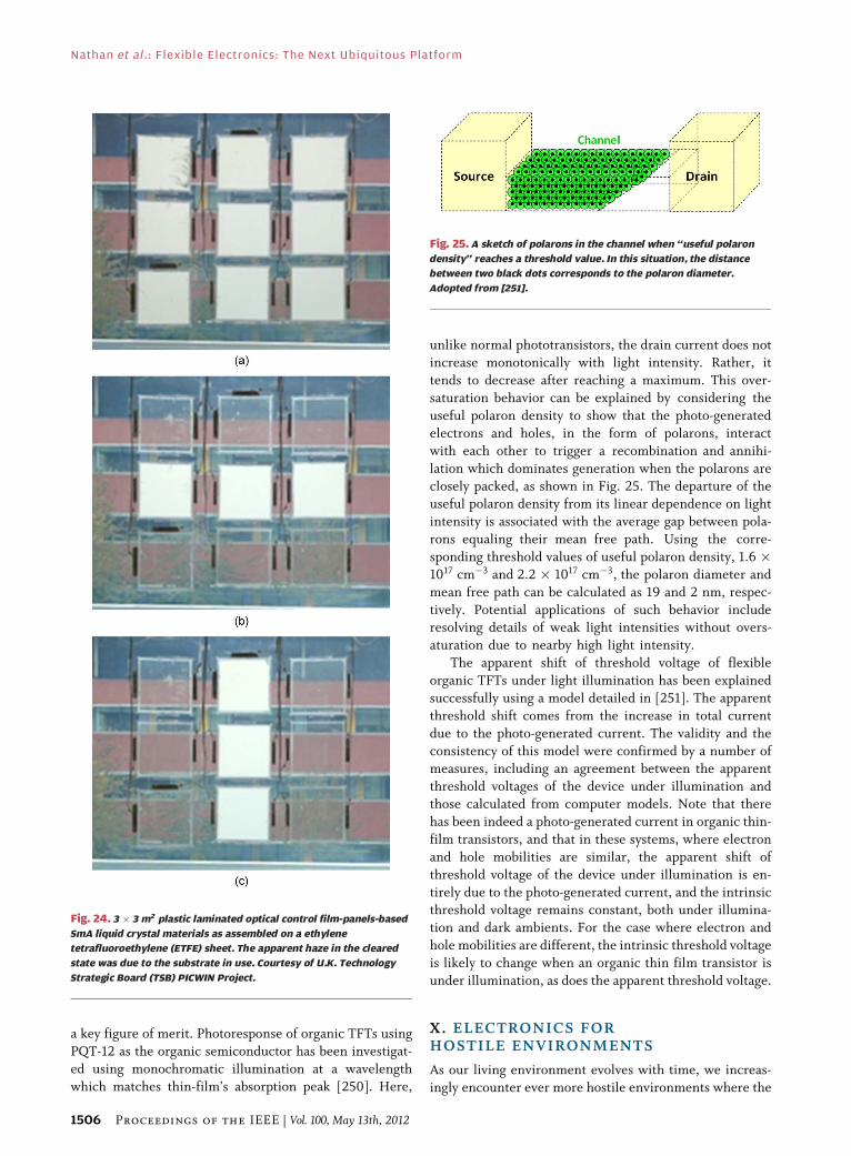
a key figure of merit. Photoresponse of organic TFTs using
PQT-12 as the organic semiconductor has been investigat-
ed using monochromatic illumination at a wavelength
which matches thin-film’s absorption peak [250]. Here,
unlike normal phototransistors, the drain current does not
increase monotonically with light intensity. Rather, it
tends to decrease after reaching a maximum. This over-
saturation behavior can be explained by considering the
useful polaron density to show that the photo-generated
electrons and holes, in the form of polarons, interact
with each other to trigger a recombination and annihi-
lation which dominates generation when the polarons areclosely packed, as shown in Fig. 25. The departure of the
useful polaron density from its linear dependence on light
intensity is associated with the average gap between pola-
rons equaling their mean free path. Using the corre-
sponding threshold values of useful polaron density, 1.6 �1017 cm�3 and 2.2 � 1017 cm�3, the polaron diameter and
mean free path can be calculated as 19 and 2 nm, respec-
tively. Potential applications of such behavior includeresolving details of weak light intensities without overs-
aturation due to nearby high light intensity.
The apparent shift of threshold voltage of flexible
organic TFTs under light illumination has been explained
successfully using a model detailed in [251]. The apparent
threshold shift comes from the increase in total current
due to the photo-generated current. The validity and the
consistency of this model were confirmed by a number ofmeasures, including an agreement between the apparent
threshold voltages of the device under illumination and
those calculated from computer models. Note that there
has been indeed a photo-generated current in organic thin-
film transistors, and that in these systems, where electron
and hole mobilities are similar, the apparent shift of
threshold voltage of the device under illumination is en-
tirely due to the photo-generated current, and the intrinsicthreshold voltage remains constant, both under illumina-
tion and dark ambients. For the case where electron and
hole mobilities are different, the intrinsic threshold voltage
is likely to change when an organic thin film transistor is
under illumination, as does the apparent threshold voltage.
X. ELECTRONICS FORHOSTILE ENVIRONMENTS
As our living environment evolves with time, we increas-
ingly encounter ever more hostile environments where the
Fig. 25. A sketch of polarons in the channel when ‘‘useful polaron
density’’ reaches a threshold value. In this situation, the distance
between two black dots corresponds to the polaron diameter.
Adopted from [251].
Fig. 24. 3 � 3 m2 plastic laminated optical control film-panels-based
SmA liquid crystal materials as assembled on a ethylene
tetrafluoroethylene (ETFE) sheet. The apparent haze in the cleared
state was due to the substrate in use. Courtesy of U.K. Technology
Strategic Board (TSB) PICWIN Project.
Nathan et al.: Flexible Electronics: The Next Ubiquitous Platform
1506 Proceedings of the IEEE | Vol. 100, May 13th, 2012
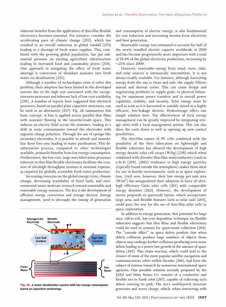
inherent benefits from the application of thin-film flexibleelectronics becomes essential. For instance, consider the
accelerating pace of climate change [252], which has
resulted in an overall reduction in global rainfall [253]
leading to a shortage of fresh water supplies. This, com-
bined with the growing global population, has put sub-
stantial pressure on existing agriculture infrastructure
leading to increased food and commodity prices [254].
One approach in mitigating the effect of fresh watershortage is conversion of abundant seawater into fresh
water via desalination [255].
Although a number of technologies exist to solve this
problem, their adoption has been limited to the developed
nations due to the high cost associated with the energy-
intensive processes and inherent lack of low-cost scalability
[256]. A number of reports have suggested that electrical
processes, based on parallel plate capacitive structures, canbe used as an alternative [257]. Fig. 26 summarizes this
basic concept. A bias is applied across parallel thin films
with seawater flowing in the interelectrode space. This
induces an electric field across the seawater, leading to a
drift in ionic contaminants toward the electrodes with
opposite charge polarities. Through the use of sponge-like
secondary electrodes, it is possible to adsorb and immobi-
lize these free ions leading to water purification. This de-salinization process, compared to other technologies
available, primarily benefits from low energy consumption.
Furthermore, the low-cost, large-area fabrication processes
inherent in thin-film flexible electronics facilitate the crea-
tion of ultrahigh throughput systems at minimal expense,
as required for globally accessible fresh water production.
Increasing concerns on the global energy crisis, climate
change, decreasing availability of fossil fuels, and envi-ronmental issues motivate research toward sustainable and
renewable energy resources. The key is the development of
efficient energy conversion and storage devices. Energy
management, used to decouple the timing of generation
and consumption of electric energy, is also fundamentalfor cost reduction and increasing income from electricity
and heat generation.
Renewable energy was estimated to account for half of
the newly installed electric capacity worldwide in 2010
and has become progressively more important with a total
of 19.4% of the global electricity production, increasing by
�21% since 2009.
However, renewable energy from wind, wave, tidal,and solar sources is intrinsically intermittent. It is not
always readily available. For instance, although harvesting
energy from the sun is clean and safe, the supply follows
annual and diurnal cycles. This can cause design and
engineering problems in supply grids, in physical balanc-
ing for maximum power transfers and in overall power
capability, stability, and security. Solar energy must be
used as soon as it is harvested or suitably stored in a highlyefficient, low-leakage devices. Hydrostorage offers one
simple solution here. The effectiveness of local energy
management can be greatly improved by integrating stor-
age units with a local management system. This can also
drive the costs down as well as opening up new control
possibilities.
The thin-film nature of PV cells combined with the
possibility of the their fabrication on lightweight andflexible substrates has allowed the development of high
energy density solar cell arrays (W/kg) [258] which when
combined with disorder thin-film semiconductors (such as
a-Si:H [259], [260]) resilience to high energy particles
(typically found outside the atmosphere) makes them ideal
for use in hostile environments, such as in space explora-
tion. Until now, however, their low energy per unit area
(W/m2) has marginalized their adoption in favor of ultra-high efficiency GaAs solar cells [261] with comparable
energy densities [262]. However, the development of
recent proposals in spacecraft layout, which incorporates
large area, and flexible features such as solar sails [263],
could pave the way for the use of thin-film solar cells in
space exploration.
In addition to energy generation, that potential for large
area, roll-to-roll, low-cost deposition technique on flexiblesubstrates suggests that thin films and flexible electronics
could be used in systems for space-waste collection [264].
The Bcascade effect[ in space debris predicts that when
debris collisions produce large numbers of objects those
objects may undergo further collisions producing even more
debris leading to a power-law growth in the amount of space
debris [265]. This chain reaction, which could lead to the
closure of some of the more popular satellite navigation andcommunications orbits within decades [266], had been the
subject of intense research by numerous international space
agencies. One possible solution recently proposed by the
JAXA and Nitto Seimo Co. consists of a conductive and
flexible net in Earth orbit [267], capable of collecting such
debris entering its path. The net’s multilayered structure
generates and stores charge, which, when interacting withFig. 26. A water desalination system with low energy consumption
based on capacitive technology.
Nathan et al.: Flexible Electronics: The Next Ubiquitous Platform
Vol. 100, May 13th, 2012 | Proceedings of the IEEE 1507
the Earth’s magnetic field, leads to a deceleration andsubsequent reduction in the net’s orbit. Eventually, the net
and debris re-enter Earth atmosphere and burn up, leaving
negligible residue. Here the durability and strength of the
net is critically important, and can be engineered through
the combination of various nanostructures while also
including appropriate coating technologies to optimize its
functionality.
Flexible electronics in hostile environments can alsofind use in military applications. Increasingly high-tech
warfare requires enhanced access to energy supplies [268].
A mechanically flexible and durable product with light-
weight mobile power harvesting system, as depicted in
Fig. 19, is one possible solution.
XI. CONCLUSION
In this paper, we have considered some of the unique
properties and applications of thin-film flexible electron-
ics. Based on the current socioeconomic trends, we out-
lined some of the more likely technological future needs
and discussed the potential exploits of thin-film flexibleelectronics in various market sectors.
We have shown that the novel properties of thin-film,
flexible electronics such as low weight, mechanical
flexibility and durability, simple device integration, along
with low-cost and large-area processability allow them to
be utilized in a wide range of applications from space
exploration to water purification, and from displays to
conformally integrated automotive batteries.Future developments in flexible thin-film technology
are likely to enhance the performance of the devices
discussed here, leading to more widespread applications.
However, it should be noted that, as with any prediction
on the scale attempted here, unforeseen global develop-
ments may lead to inaccuracies in some of the
assumptions made. h
Acknowledgment
The authors would like to thank P. Beecher and
Z. Radivojevic for useful discussions.
REFERENCES
[1] T. D. Anthopoulos, S. Setayesh, E. Smits,M. Colle, E. Cantatore, B. de Boer,P. W. M. Blom, and D. M. de Leeuw,BAir-stable complementary-like circuitsbased on organic ambipolar transistors,[Adv. Mater., vol. 18, no. 14, pp. 1900–1904,Jul. 2006.
[2] H. Yin, S. Kim, C. J. Kim, J. C. Park,I. Song, S.-W. Kim, S.-H. Lee, and Y. Park,BBootstrapped ring oscillator withpropagation delay time below 1.0 nsec/stageby standard 0.5�m bottom-gate amorphousGa2O3-In2O3-ZnO TFT technology,[ inProc. Electron Devices Meeting, San Francisco,CA, 2008, DOI: 10.1109/IEDM.2008.4796619.
[3] G. Kawachi, Y. Nakazaki, H. Ogawa,M. Jyumonji, N. Akita, M. Hiramatu,K. Azuma, T. Warabisako, andM. Matsumura, BCharacterization ofhigh-performance polycrystalline siliconcomplementary metal-oxide-semiconductorcircuits,[ Jpn. J. Appl. Phys., vol. 46, no. 1,pp. 51–55, Jan. 2007.
[4] R. Hayashi, M. Ofuji, N. Kaji, K. Takahashi,K. Abe, H. Yabuta, M. Sano, H. Kumomi,K. Nomura, T. Kamiya, M. Hirano, andH. Hosono, BCircuits using uniform TFTsbased on amorphous In-Ga-Zn-O,[ J. Soc.Inf. Display, vol. 15, no. 11, pp. 915–921,2007.
[5] D. J. Gundlach, J. E. Royer, S. K. Park,S. Subramanian, O. D. Jurchescu,B. H. Hamadani, A. J. Moad, R. J. Kline,L. C. Teague, O. Kirillov, C. A. Richter,J. G. Kushmerick, L. J. Richter, S. R. Parkin,T. N. Jackson, and J. E. Anthony,BContact-induced crystallinity forhigh-performance soluble acene-basedtransistors and circuits,[ Nature Mater.,vol. 7, no. 3, pp. 216–221, Feb. 2008.
[6] R. E. Proano, R. S. Misage, andD. G. Ast, BDevelopment and electricalproperties of undoped polycrystalline siliconthin-film transistors,[ IEEE Trans. ElectronDevices, vol. 36, no. 9, pp. 1915–1922,Sep. 1989.
[7] H. Hayashi, M. Kunii, M. Suzuki, Y. Kanaya,M. Kuki, M. Minegishi, T. Urazono,M. Fujino, T. Noguchi, and M. Yamazaki,BFabrication of low-temperature bottom-gatepoly-Si TFTs on large-area substrate bylinear-beam excimer laser crystallization andion doping method,[ in Proc. Int. ElectronDevices Meeting, Dec. 10–13, 1995,pp. 829–832.
[8] A. Suresh, P. Wellenius, V. Baliga, H. Luo,L. M. Lunardi, and J. F. Muth, BFastall-transparent integrated circuits basedon indium gallium zinc oxide thin-filmtransistors,[ IEEE Electron Device Lett.,vol. 31, no. 4, pp. 317–319, Apr. 2010.
[9] D. Zhao, D. A. Mourey, and T. N. Jackson,BFast flexible plastic substrate ZnO circuits,[IEEE Electron Device Lett., vol. 31, no. 4,pp. 323–325, Apr. 2010.
[10] M. Ofuji, K. Abe, H. Shimizu, N. Kaji,R. Hayashi, M. Sano, H. Kumomi,K. Nomura, T. Kamiya, and H. Hosono,BFast thin-film transistor circuits basedon amorphous oxide semiconductor,[IEEE Electron Device Lett., vol. 28, no. 4,pp. 273–275, Apr. 2007.
[11] S. D. Brotherton, C. Glasse, C. Glaister,P. Green, F. Rohlfing, and J. R. Ayres,BHigh-speed, short-channel polycrystallinesilicon thin-film transistors,[ Appl. Phys.Lett., vol. 84, no. 2, pp. 293–295, 2004.
[12] T. Noguchi, H. Hayashi, andT. Ohshima, BLow temperature polysiliconsuper-thin-film transistor (LSFT),[Jpn. J. Appl. Phys., vol. 25, no. 2, pt. 2,pp. L121–L123, Feb. 1986.
[13] F. Eder, H. Klauk, M. Halik,U. Zschieschang, G. Schmid, and C. Dehm,BOrganic electronics on paper,[ Appl. Phys.Lett., vol. 84, no. 14, pp. 2673–2675, 2004.
[14] P. F. Baude, D. A. Ender, M. A. Haase,T. W. Kelley, D. V. Muyres, and S. D. Theiss,BPentacene-based radio-frequencyidentification circuitry,[ Appl. Phys. Lett.,vol. 82, no. 22, pp. 3964–3966, 2003.
[15] D. Zielke, A. C. Hubler, U. Hahn, N. Brandt,M. Bartzsch, U. Fugmann, T. Fischer,J. Veres, and S. Ogier, BPolymer-based
organic field-effect transistor using offsetprinted source/drain structures,[ Appl. Phys.Lett., vol. 87, no. 12, pp. 123508-1–123508-3,2005.
[16] A. C. Huebler, F. Doetz, H. Kempa,H. E. Katz, M. Bartzsch, N. Brandt,I. Hennig, U. Fuegmann, S. Vaidyanathan,J. Granstrom, S. Liu, A. Sydorenko,T. Zillger, G. Schmidt, K. Preissler,E. Reichmanis, P. Eckerle, F. Richter,T. Fischer, and U. Hahn, BRing oscillatorfabricated completely by means ofmass-printing technologies,[ OrganicElectron., vol. 8, no. 5, pp. 480–486,Oct. 2007.
[17] K. H. Cherenack, B. Hekmatshoar,J. C. Sturm, and S. Wagner, BSelf-alignedamorphous silicon thin-film transistorsfabricated on clear plastic at 300 �C,[ IEEETrans. Electron Devices, vol. 57, no. 10,pp. 2381–2389, Oct. 2010.
[18] K. Hiranaka, T. Yamaguchi, andS. Yanagisawa, BSelf-alignment processedamorphous silicon ring oscillators,[IEEE Electron Device Lett., vol. 5, no. 7,pp. 224–225, Jul. 1984.
[19] S. K. Park, J. E. Anthony, and T. N. Jackson,BSolution-processed TIPS-pentacene organicthin-film-transistor circuits,[ IEEE ElectronDevice Lett., vol. 28, no. 10, pp. 877–879,Oct. 2007.
[20] R. E. Presley, D. Hong, H. Q. Chiang,C. M. Hung, R. L. Hoffman, and J. F. Wager,BTransparent ring oscillator based onindium gallium oxide thin-film transistors,[Solid-State Electron., vol. 50, no. 3,pp. 500–503, Mar. 2006.
[21] D. B. Thomasson, M. Bonse, J.-R. Huang,C. R. Wronski, and T. N. Jackson, BTri-layera-Si:H integrated circuits on polymericsubstrates,[ in Tech. Dig. Int. Electron DevicesMeeting, Dec. 6–9, 1998, pp. 253–256.
[22] P. Servati, A. Nathan, andG. A. J. Amaratunga, BGeneralizedtransport-band field-effect mobility indisordered organic and inorganicsemiconductors,[ Phys. Rev. B,vol. 74, no. 24, Dec. 2006, 245210.
Nathan et al.: Flexible Electronics: The Next Ubiquitous Platform
1508 Proceedings of the IEEE | Vol. 100, May 13th, 2012
[23] A. Ahnood, K. Ghaffarzadeh, A. Nathan,P. Servati, F. Li, M. R. Esmaeili-Rad, andA. Sazonov, BNon-ohmic contact resistanceand field-effect mobility in nanocrystallinesilicon thin film transistors,[ Appl. Phys. Lett.,vol. 93, no. 16, pp. 163503-1–163503-3,Oct. 2008.
[24] J. Stott, A. Kumatani, T. Minari,K. Tsukagoshi, S. Heutz, G. Aeppli, andA. Nathan, BBottom-contact pentacenethin-film transistors on silicon nitride,[IEEE Electron Device Lett., vol. 32, no. 9,pp. 1305–1307, Sep. 2011.
[25] A. Ahnood, G. R. Chaji, A. Sazonov, andA. Nathan, BEffect of threshold voltageinstability on field effect mobility in thin filmtransistors deduced from constant currentmeasurements,[ Appl. Phys. Lett., vol. 95,no. 6, pp. 063506-1–063506-3, 2009.
[26] S. Y. Park, B. J. Kim, K. Kim, M. S. Kang,K.-H. Lim, T. I. Lee, J. M. Myoung,H. K. Baik, J. H. Cho, and Y. S. Kim,BLow-temperature, solution-processedand alkali metal doped ZnO forhigh-performance thin-film transistors,[Adv. Mater., vol. 24, no. 6, pp. 834–838,Feb. 2012.
[27] R. G. Gordon, BCriteria for choosingtransparent conductors,[ Mater. Res. Soc.Bull., vol. 25, no. 08, pp. 52–57, Jan. 2011.
[28] K. H. Kim, S. J. Park, A. Y. Kim, andJ. Jang, BGrowth of large-grain poly-Siby FE-SMC,[ J. Non-Crystalline Solids,vol. 299–302, pp. 3–86, Apr. 2002.
[29] S. Y. Yoon, S. J. Park, K. H. Kim, and J. Jang,BMetal-induced crystallization of amorphoussilicon,[ Thin Solid Films, vol. 383, no. 1–2,pp. 34–38, Feb. 2001.
[30] H. J. Lee, A. Sazonov, and A. Nathan,BLeakage current mechanisms in top-gatenanocrystalline silicon thin film transistors,[Appl. Phys. Lett., vol. 92, no. 8, 2008,083509.
[31] F. M. Li, G.-W., Hsieh, S. Dalal,M. C. Newton, J. E. Stott, P. Hiralal,A. Nathan, P. A. Warburton, H. E. Unalan,P. Beecher, A. J. Flewitt, I. Robinson,G. Amaratunga, and W. I. Milne, BZinc oxidenanostructures and high electron mobilitynanocomposite thin film transistors,[ IEEETrans. Electron Devices, vol. 55, no. 11,pp. 3001–3011, Nov. 2008.
[32] Y. D. Park, J. A. Lim, Y. Jang, M. Hwang,H. S. Lee, D. H. Lee, H.-J. Lee, J.-B. Baek,and K. Cho, BEnhancement of the field-effectmobility of poly(3-hexylthiophene)/functionalized carbon nanotube hybridtransistors,[ Organic Electron., vol. 9, no. 3,pp. 317–322, Jun. 2008.
[33] S.-H. Hur, O. O. Park, and J. A. Rogers,BExtreme bendability of single-walledcarbon nanotube networks transferredfrom high-temperature growth substrates toplastic and their use in thin-film transistors,[Appl. Phys. Lett., vol. 86, no. 24, 2005,243502.
[34] G.-W. Hsieh, J. Wang, K. Ogata,J. Robertson, S. Hofmann, andW. I. Milne, BStretched contact printing ofone-dimensional nanostructures for hybridinorganic-organic field effect transistors,[J. Phys. Chem. C, vol. 116, no. 12,pp. 7118–7125, Feb. 2012.
[35] M. R. Esmaeili-Rad, F. Li, A. Sazonov, andA. Nathan, BStability of nanocrystallinesilicon bottom-gate thin film transistors withsilicon nitride gate dielectric,[ J. Appl. Phys.,vol. 102, no. 6, 2007, 064512.
[36] M. Bauza, A. Ahnood, F. M. Li,Y. Vygranenko, M. R. Esmaeili-Rad, G. Chaji,
A. Sazonov, J. Robertson, W. I. Milne, andA. Nathan, BPhoto-induced instability ofnanocrystalline silicon TFTs,[ IEEE J. DisplayTechnol., vol. 6, no. 12, pp. 589–591,Dec. 2010.
[37] K. Ghaffarzadeh, A. Nathan, J. Robertson,S. Kim, S. Jeon, C. Kim, U.-I. Chung, andJ.-H. Lee, BInstability in threshold voltageand subthreshold behavior in Hf-In-Zn-Othin film transistors induced by bias-andlight-stress,[ Appl. Phys. Lett., vol. 97,pp. 113504-1–113504-3, no. 11, 2010,113504.
[38] M. Bauza, N. P. Mandal, A. Ahnood,A. Sazonov, and A. Nathan, BLight-inducedmetastability in thin nanocrystalline siliconfilms,[ Philosoph. Mag., vol. 89, no. 28,p. 2531, 2009.
[39] Y.-M. Lin, K. A. Jenkins, A. Valdes-Garcia,J. P. Small, D. B. Farmer, and P. Avouris,BOperation of graphene transistors atgigahertz frequencies,[ Nano Lett., vol. 9,no. 1, pp. 422–426, Jan. 2009.
[40] A. K. Geim and K. S. Novoselov, BThe riseof graphene,[ Nature Mater., vol. 6, no. 3,pp. 183–191, Mar. 2007.
[41] B. Radisavljevic, A. Radenovic, J. Brivio,V. Giacometti, and A. Kis, BSingle-layerMoS2 transistors,[ Nature Nanotechnol.,vol. 6, no. 3, pp. 147–150, Jan. 2011.
[42] L. Song, L. Ci, H. Lu, P. B. Sorokin, C. Jin,J. Ni, A. G. Kvashnin, D. G. Kvashnin, J. Lou,B. I. Yakobson, and P. M. Ajayan, BLargescale growth and characterization of atomichexagonal boron nitride layers,[ Nano Lett.,vol. 10, no. 8, pp. 3209–3215, Aug. 2010.
[43] M. Moradi, A. A. Fomani, and A. Nathan,BEffect of gate dielectric scaling innanometer scale vertical thin filmtransistors,[ Appl. Phys. Lett., vol. 99, no. 22,2011, 223503.
[44] S. P. Li, D. P. Chu, C. J. Newsome,D. M. Russell, T. Kugler, M. Ishida, andT. Shimoda, BShort-channel polymerfield-effect-transistor fabrication usingspin-coating-induced edge template andink-jet printing,[ Appl. Phys. Lett., vol. 87,no. 23, 2005, 232111.
[45] T. Takenobu, N. Miura, S.-Y. Lu,H. Okimoto, T. Asano, M. Shiraishi, andY. Iwasa, BInk-jet printing of carbonnanotube thin-film transistors on flexibleplastic substrates,[ Appl. Phys. Exp., vol. 2,Feb. 2009, 025005.
[46] F. Torrisi, T. Hasan, W. Wu, Z. Sun,A. Lombardo, T. Kulmala, G. W. Hshieh,S. J. Jung, F. Bonaccorso, P. J. Paul,D. P. Chu, and A. C. Ferrari, BInk-jet printedgraphene electronics,[ ACS Nano, vol. 6,no. 4, pp. 2992–3006, Apr. 2012.
[47] S. Li, W. Chen, D. Chu, and S. Roy,BSelf-aligned high-resolution printedpolymer transistors,[ Adv. Mater., vol. 23,no. 35, pp. 4107–4110, Sep. 2011.
[48] M. J. Kelly, BIntrinsic top-downunmanufacturability,[ Nanotechnology,vol. 22, no. 24, Jun. 2011, 245303.
[49] G.-W. Hsieh, F. M. Li, P. Beecher,A. Nathan, Y. Wu, B. S. Ong, andW. I. Milne, BHigh performancenanocomposite thin film transistors withbilayer carbon nanotube-polythiopheneactive channel by ink-jet printing,[ J. Appl.Phys., vol. 106, no. 12, 2009, 123706.
[50] T. Hasan, Z. Sun, F. Wang, F. Bonaccorso,P. H. Tan, A. G. Rozhin, and A. C. Ferrari,BNanotubea-polymer composites for ultrafastphotonics,[ Adv. Mater., vol. 21, no. 38–39,pp. 3874–3899, Oct. 2009.
[51] Z. Sun, T. Hasan, F. Torrisi, D. Popa,G. Privitera, F. Wang, F. Bonaccorso,D. M. Basko, and A. C. Ferrari, BGraphenemode-locked ultrafast laser,[ ACS Nano,vol. 4, no. 2, pp. 803–810, Feb. 2010.
[52] F. Bonaccorso, Z. Sun, T. Hasan, andA. C. Ferrari, BGraphene photonicsand optoelectronics,[ Nature Photon.,vol. 4, no. 9, pp. 611–622, Aug. 2010.
[53] M. Reibold, P. Paufler, A. A. Levin,W. Kochmann, N. Patzke, and D. C. Meyer,BMaterials: Carbon nanotubes in an ancientDamascus sabre,[ Nature, vol. 444, no. 7117,pp. 286–286, Nov. 2006.
[54] M. Martinon-Torres, T. Rehren, andI. C. Freestone, BMullite and the mystery ofHessian wares,[ Nature, vol. 444, no. 7118,pp. 437–438, Nov. 2006.
[55] M. Reibold, P. Paufler, A. A. Levin,W. Kochmann, N. Patzke, and D. C. Meyer,BMaterials: Carbon nanotubes in an ancientDamascus sabre,[ Nature, vol. 444, no. 7117,pp. 286–286, Nov. 2006.
[56] M. Martinon-Torres, T. Rehren, andI. C. Freestone, BMullite and the mystery ofHessian wares,[ Nature, vol. 444, no. 7118,pp. 437–438, Nov. 2006.
[57] A. Stierle and A. M. Molenbroek, BNovelin situ probes for nanocatalysis,[ Mater. Res.Soc. Bull., vol. 32, no. 12, pp. 1001–1009,Jan. 2011.
[58] S. Hofmann, R. Sharma, C. Ducati, G. Du,C. Mattevi, C. Cepek, M. Cantoro, S. Pisana,A. Parvez, F. Cervantes-Sodi, A. C. Ferrari,R. Dunin-Borkowski, S. Lizzit, L. Petaccia,A. Goldoni, and J. Robertson, BIn situobservations of catalyst dynamics duringsurface-bound carbon nanotube nucleation,[Nano Lett., vol. 7, no. 3, pp. 602–608,Mar. 2007.
[59] S. Hofmann, R. Sharma, C. T. Wirth,F. Cervantes-Sodi, C. Ducati, T. Kasama,R. E. Dunin-Borkowski, J. Drucker,P. Bennett, and J. Robertson,BLedge-flow-controlled catalyst interfacedynamics during Si nanowire growth,[Nature Mater., vol. 7, no. 5, pp. 372–375,Mar. 2008.
[60] P. L. Gai, R. Sharma, and F. M. Ross,BEnvironmental (S)TEM studies ofgas-liquid-solid interactions under reactionconditions,[ Mater. Res. Soc. Bull., vol. 33,no. 02, pp. 107–114, Jan. 2011.
[61] S. Hofmann, R. Blume, C. T. Wirth,M. Cantoro, R. Sharma, C. Ducati,M. Havecker, S. Zafeiratos, P. Schnoerch,A. Oestereich, D. Teschner, M. Albrecht,A. Knop-Gericke, R. Schlogl, andJ. Robertson, BState of transition metalcatalysts during carbon nanotube growth,[ J.Phys. Chem. C, vol. 113, no. 5, pp. 1648–1656,Feb. 2009.
[62] R. S. Weatherup, B. C. Bayer, R. Blume,C. Ducati, C. Baehtz, R. Schlogl, andS. Hofmann, BIn situ characterization ofalloy catalysts for low-temperature graphenegrowth,[ Nano Lett., vol. 11, no. 10,pp. 4154–4160, Oct. 2011.
[63] D.-H. Kim, J. Xiao, J. Song, Y. Huang, andJ. A. Rogers, BStretchable, curvilinearelectronics based on inorganic materials,[Adv. Mater., vol. 22, no. 19, pp. 2108–2124,Jan. 2010.
[64] S. P. Lacour, S. Wagner, Z. Huang, andZ. Suo, BStretchable gold conductorson elastomeric substrates,[ Appl. Phys.Lett., vol. 82, no. 15, pp. 2404–2406,2003.
[65] A. Flewitt and A. Nathan, BThin-film siliconmaterials and devices for large-area and
Nathan et al.: Flexible Electronics: The Next Ubiquitous Platform
Vol. 100, May 13th, 2012 | Proceedings of the IEEE 1509
flexible solar cells and electronics,[ inTutorial, MRS Spring Meeting, San Francisco,CA, 2009.
[66] R. Martins, A. Nathan, R. Barros, L. Pereira,P. Barquinha, N. Correia, R. Costa,A. Ahnood, I. Ferreira, and E. Fortunato,BComplementary metal oxide semiconductortechnology with and on paper,[ Adv. Mater.,vol. 23, no. 39, pp. 4491–4496, Oct. 2011.
[67] J. Hiner, Good Product Desing: The10 Principles of Dieter Rams, Oct. 9, 2011.[Online]. Available: http://www.jasonhiner.com/blog/2011/10/9/good-product-design-the-10-principles-of-dieter-rams.html
[68] P. Kotler and G. A. Rath, BDesign:A powerful but neglected strategic tool,[J. Business Strategy, vol. 5, no. 2, pp. 16–21,1984.
[69] G. Gemser, BHow integrating industrialdesign in the product development processimpacts on company performance,[ J.Product Innovation Manage., vol. 18, no. 1,pp. 28–38, Jan. 2001.
[70] J. H. Hertenstein, M. B. Platt, andD. R. Brown, BValuing design: Enhancingcorporate performance through designeffectiveness,[ Design Manage. J. (FormerSer.), vol. 12, no. 3, pp. 10–19, Jun. 2010.
[71] G. Cox, BCox review of creativity in business:Building on the UK’s strengths,[ HMTreasury, London, U.K., Executive Summary,2005.
[72] D. Sainsbury, BThe race to the top: A reviewof Government’s science and innovationpolicies,[ HM Treasury, London, U.K., 2007.
[73] C. Enterprise, BPlastic logic introducesthe plastic logic 100, bringing innovationto the future of education in Russia,[Sep. 21, 2011.
[74] N. Kumarchauhan, BPhilips fluidsmartphone with flexible OLED display,[Aug. 18, 2010.
[75] F. Axisa, P. M. Schmitt, C. Gehin,G. Delhomme, E. McAdams, and A. Dittmar,BFlexible technologies and smart clothingfor citizen medicine, home healthcare, anddisease prevention,[ IEEE Trans. Inf. Technol.Biomed., vol. 9, no. 3, pp. 325–336,Sep. 2005.
[76] R. S. H. Istepanian, E. Jovanov, andY. T. Zhang, BGuest editorial introductionto the special section on m-health: Beyondseamless mobility and global wirelesshealth-care connectivity,[ IEEE Trans. Inf.Technol. Biomed., vol. 8, no. 4, pp. 405–414,Dec. 2004.
[77] S. S. Lane, B. D. Kuppermann, I. H. Fine,M. B. Hamill, J. F. Gordon, R. S. Chuck,R. S. Hoffman, M. Packer, and D. D. Koch,BA prospective multicenter clinical trial toevaluate the safety and effectiveness of theimplantable miniature telescope,[ Amer. J.Ophthalmol., vol. 137, no. 6, pp. 993–1001,Jun. 2004.
[78] C. W. Turner, B. J. Gantz, C. Vidal,A. Behrens, and B. A. Henry, BSpeechrecognition in noise for cochlear implantlisteners: Benefits of residual acoustichearing,[ J. Acoust. Soc. Amer., vol. 115, no. 4,pp. 1729–1735, 2004.
[79] T. Guenther, N. H. Lovell, and G. J. Suaning,BBionic vision: System architecturesVAreview,[ Expert Rev. Med. Devices, vol. 91,pp. 33–48, Jan. 2012.
[80] D. Purves, Neuroscience. Sunderland, MA:Sinauer, 2008.
[81] P. M. Chute and M. E. Nevins, The Parents’Guide to Cochlear Implants. Washington,DC: Gallaudet Univ. Press, 2002.
[82] S. Frings and J. Bradley, TransductionChannels in Sensory Cells. Weinheim,Germany: Wiley-VCH, 2004, p. 155.
[83] F. M. Matschinsky, BBanting lecture 1995.A lesson in metabolic regulation inspired bythe glucokinase glucose sensor paradigm,[Diabetes, vol. 45, no. 2, pp. 223–241,Feb. 1996.
[84] N. Chaudhari, H. Yang, C. Lamp, E. Delay,C. Cartford, T. Than, and S. Roper, BThetaste of monosodium glutamate: Membranereceptors in taste buds,[ J. Neurosci., vol. 16,no. 12, pp. 3817–3826, Jun. 1996.
[85] J. B. Baxter and E. S. Aydil, BNanowire-baseddye-sensitized solar cells,[ Appl. Phys. Lett.,vol. 86, no. 5, 2005, 053114.
[86] M. Law, L. E. Greene, J. C. Johnson,R. Saykally, and P. Yang, BNanowiredye-sensitized solar cells,[ Nature Mater.,vol. 4, no. 6, pp. 455–459, May 2005.
[87] H. Rensmo, K. Keis, H. Lindstrom,S. Sodergren, A. Solbrand, A. Hagfeldt,S.-E. Lindquist, L. N. Wang, andM. Muhammed, BHigh light-to-energyconversion efficiencies for solar cells basedon nanostructured ZnO electrodes,[ J. Phys.Chem. B, vol. 101, no. 14, pp. 2598–2601,Apr. 1997.
[88] K. Myny, S. Steudel, P. Vicca,M. J. Beenhakkers, N. A. J. M. van Aerle,G. H. Gelinck, J. Genoe, W. Dehaene, andP. Heremans, BPlastic circuits and tagsfor 13.56 MHz radio-frequencycommunication,[ Solid-State Electron.,vol. 53, no. 12, pp. 1220–1226, Dec. 2009.
[89] M. Kaempgen, C. K. Chan, J. Ma, Y. Cui, andG. Gruner, BFilm supercapacitors usingsingle-walled carbon nanotubes,[ Nano Lett.,vol. 9, no. 5, pp. 1872–1876, May 2009.
[90] J. B. Bates, N. J. Dudney, B. Neudecker,A. Ueda, and C. D. Evans, BThin-film lithiumand lithium-ion batteries,[ Solid State Ionics,vol. 135, no. 1–4, pp. 33–45, Nov. 2000.
[91] J. G. E. Gardeniers and A. van den Berg,BLab-on-a-chip systems for biomedical andenvironmental monitoring,[ Anal. Bioanal.Chem., vol. 378, no. 7, pp. 1700–1703,Apr. 2004.
[92] V. Srinivasan, V. K. Pamula, and R. B. Fair,BAn integrated digital microfluidiclab-on-a-chip for clinical diagnostics onhuman physiological fluids,[ Lab-on-a-Chip,vol. 4, no. 4, pp. 310–315, 2004.
[93] B. H. Weigl, R. L. Bardell, and C. R. Cabrera,BLab-on-a-chip for drug development,[Adv. Drug Delivery Rev., vol. 55, no. 3,pp. 349–377, Feb. 2003.
[94] Y. Q. Fu, J. K. Luo, X. Y. Du, A. J. Flewitt,Y. Li, G. H. Markx, A. J. Walton, andW. I. Milne, BRecent developments on ZnOfilms for acoustic wave based bio-sensingand microfluidic applications: A review,[Sens. Actuators B, Chem., vol. 143, no. 2,pp. 606–619, Jan. 2010.
[95] X. Y. Du, Y. Q. Fu, J. K. Luo, A. J. Flewitt,and W. I. Milne, BMicrofluidic pumpsemploying surface acoustic waves generatedin ZnO thin films,[ J. Appl. Phys., vol. 105,no. 2, 2009, 024508.
[96] J. Luo, Y. R. Fu, X. Du, D. Lee, S. Maeng,A. Flewitt, and B. Milne, BZnO thin filmsurface acoustic wave based lab-on-a-chip,[in Proc. Mater. Res. Soc. Symp., Jan. 2011,vol. 1222, 1222-DD01-05.
[97] D. S. Lee, Y. Q. Fu, S. Maeng, X. Y. Du,S. C. Tan, J. K. Luo, A. J. Flewitt, S. H. Kim,N. M. Park, Y. J. Choi, H. C. Yoon, S. Y. Oh,and W. I. Milne, BIntegrated ZnO surfaceacoustic wave microfluidic and biosensor
system,[ in Proc. IEEE Int. Electron DevicesMeeting, Dec. 10–12, 2007, pp. 851–854.
[98] J. K. Luo, G. M. Ashley, L. G. Gancedo,P. B. Kirby, A. J. Flewitt, and W. I. Milne,BFilm bulk acoustic resonator nanosensorsfor multi-task sensing,[ Int. J. Nanomanufact.,vol. 7, no. 5/6, pp. 448–462, 2011.
[99] L. Garcia-Gancedo, F. Al-Naimi, A. Flewitt,W. Wilne, G. Ashley, J. Luo, X. Zhao, andJ. Lu, BZnO-based FBAR resonators withcarbon nanotube electrodes,[ IEEE Trans.Ultrason. Ferroelectr. Freq. Control, vol. 58,no. 11, pp. 2438–2445, Nov. 2011.
[100] R. Truckenmuller, S. Giselbrecht,C. van Blitterswijk, N. Dambrowsky,E. Gottwald, T. Mappes, A. Rolletschek,V. Saile, C. Trautmann, K.-F. Weibezahn,and A. Welle, BFlexible fluidic microchipsbased on thermoformed and locally modifiedthin polymer films,[ Lab-on-a-Chip, vol. 8,no. 9, pp. 1570–1579, 2008.
[101] M. Focke, D. Kosse, C. Muller, H. Reinecke,R. Zengerle, and F. von Stetten,BLab-on-a-foil: Microfluidics on thin andflexible films,[ Lab Chip, vol. 10, no. 11,pp. 1365–1386, Jun. 2010.
[102] C. J. Rydh and B. A. Sanden, BEnergyanalysis of batteries in photovoltaicsystems. Part I: Performance and energyrequirements,[ Energy Conv. Manage.,vol. 46, no. 11–12, pp. 1957–1979, Jul. 2005.
[103] G. Mom, The Electric Vehicle: Technologyand Expectations in the Automobile Age.Baltimore, MD: Johns Hopkins Univ. Press,2004.
[104] M. S. Dresselhaus and I. L. Thomas,BAlternative energy technologies,[ Nature,vol. 414, no. 6861, pp. 332–337, Nov. 2001.
[105] C. C. Chan, BThe state of the art of electric,hybrid, and fuel cell vehicles,[ Proc. IEEE,vol. 95, no. 4, pp. 704–718, Apr. 2007.
[106] J. Romm, BThe car and fuel of the future,[Energy Policy, vol. 34, no. 17, pp. 2609–2614,Nov. 2006.
[107] A. S. Arico, P. Bruce, B. Scrosati,J.-M. Tarascon, and W. van Schalkwijk,BNanostructured materials for advancedenergy conversion and storage devices,[Nature Mater., vol. 4, no. 5, pp. 366–377,May 2005.
[108] P. A. Nelson and J. R. Owen, BAhigh-performance supercapacitor/batteryhybrid incorporating templated mesoporouselectrodes,[ J. Electrochem. Soc., vol. 150,no. 10, pp. A1313–A1317, 2003.
[109] P. Liu, E. Sherman, and A. Jacobsen, BDesignand fabrication of multifunctional structuralbatteries,[ J. Power Sources, vol. 189, no. 1,pp. 646–650, Apr. 2009.
[110] J. F. Snyder, R. H. Carter, and E. D. Wetzel,BElectrochemical and mechanical behaviorin mechanically robust solid polymerelectrolytes for use in multifunctionalstructural batteries,[ Chem. Mater., vol. 19,no. 15, pp. 3793–3801, Jul. 2007.
[111] L. Christodoulou and J. D. Venables,BMultifunctional material systems: The firstgeneration,[ JOM J. Minerals Metals Mater.Soc., vol. 55, no. 12, pp. 39–45, Dec. 2003.
[112] J. P. Thomas and M. A. Qidwai, BThedesign and application of multifunctionalstructure-battery materials systems,[ JOM J.Minerals Metals Mater. Soc., vol. 57, no. 3,pp. 18–24, Mar. 2005.
[113] O. Berder, P. Quemerais, O. Sentieys,J. Astier, T. D. Nguyen, J. Menard,G. Le Mestre, Y. Le Roux, Y. Kokar,G. Zaharia, R. Benzerga, X. Castel,M. Himdi, G. E. Zein, S. Jegou,
Nathan et al.: Flexible Electronics: The Next Ubiquitous Platform
1510 Proceedings of the IEEE | Vol. 100, May 13th, 2012
P. Cosquer, and M. Bernard, BCooperativeCommunications Between Vehicles andIntelligent Road Signs,[ in Proc. 8th Int. Conf.ITS Telecommun., Oct. 24, 2008, pp. 121–126.
[114] IPENZ Conference, Institution ofProfessional Engineers New Zealand., andCSP Pacific (Firm)Engineering, Providingthe Foundations for Society, Wellington,New Zealand, Papers Presented in theTechnical Programme, Feb.9–13, 1996.
[115] J.-M. Liu, T. M. Lee, C.-H. Wen, andC.-M. Leu, BHigh-performanceorganic-inorganic hybrid plastic substratefor flexible displays and electronics,[ J. Soc.Inf. Display, vol. 19, no. 1, pp. 63–69, 2011.
[116] T. Yamada, Y. Tsubata, C. Sekine, andT. Ohnishi, BInvited paper: Recent progressin light-emitting polymers for full colorOLEDs,[ in SID Symp. Dig. Tech. Papers,2008, vol. 39, no. 1, pp. 404–406.
[117] M.-C. Choi, Y. Kim, and C.-S. Ha, BPolymersfor flexible displays: From material selectionto device applications,[ Progr. Polymer Sci.,vol. 33, no. 6, pp. 581–630, Jun. 2008.
[118] S. Utsunomiya, T. Kamakura, M. Kasuga,M. Kimura, W. Miyazawa, S. Inoue, andT. Shimoda, B21.3: Flexible color AM-OLEDdisplay fabricated using Surface FreeTechnology by Laser Ablation/Annealing(SUFTLA) and ink-jet printing technology,[in SID Symp. Dig. Tech. Papers, 2003, vol. 34,no. 1, pp. 864–867.
[119] R. Street, W. Wong, S. Ready, M. Chabinyc,A. Arias, S. Limb, A. Salleo, and R. Lujan,BJet printing flexible displays,[Mater. Today,vol. 9, no. 4, pp. 32–37, Apr. 2006.
[120] B.-J. de Gans, P. C. Duineveld, andU. S. Schubert, BInkjet printing of polymers:State of the art and future developments,[Adv. Mater., vol. 16, no. 3, pp. 203–213,Feb. 2004.
[121] Y.-Y. Noh, X. Cheng, H. Sirringhaus,J. I. Sohn, M. E. Welland, and D. J. Kang,BInk-jet printed ZnO nanowire field effecttransistors,[ Appl. Phys. Lett., vol. 91, no. 4,2007043109.
[122] P. Beecher, P. Servati, A. Rozhin, A. Colli,V. Scardaci, S. Pisana, T. Hasan, A. J. Flewitt,J. Robertson, G. W. Hsieh, F. M. Li,A. Nathan, A. C. Ferrari, and W. I. Milne,BInk-jet printing of carbon nanotube thinfilm transistors,[ J. Appl. Phys., vol. 102, no. 4,2007, 043710.
[123] W. Westerman, J. Elisa, and A. Hedge,BMulti-touch: A new tactile 2D gestureinterface for human-computer interaction,[in Proc. Human Factors Ergonom. Soc. Annu.Meeting, 2001, vol. 1, pp. 632–636.
[124] W. Westerman, BHand tracking, fingeridentification, and chordic manipulation ona multi-touch surface,[ Ph.D. dissertation.Dept. Elec. Eng., Univ. Delaware, Newark,DE, 1999.
[125] T. Kaaresoja and J. Linjama, BPerception ofshort tactile pulses generated by a vibrationmotor in a mobile phone,[ in Proc.Eurohaptics Conf./Symp. Haptic InterfacesVirtual Environ. Teleoperator Syst.,Mar. 18–20, 2005, pp. 471–472.
[126] L. M. Brown and T. Kaaresoja, BFeelwho’s talking,[ in Proc. Extended AbstractsConf. Human Factors Comput. Syst., 2006,pp. 604–609.
[127] E. Hoggan, S. A. Brewster, and J. Johnston,BInvestigating the effectiveness of tactilefeedback for mobile touchscreens,[ in Proc.Conf. Human Factors Comput. Syst., 2008,pp. 1573–1582.
[128] T.-H. Yang, D. Pyo, S.-Y. Kim, Y.-J. Cho,Y. D. Bae, Y. M. Lee, J. S. Lee, E. H. Lee, and
D.-S. Kwon, BA new subminiature impactactuator for mobile devices,[ in Proc. IEEEWorld Haptics Conf., Jun. 21–24, 2011,pp. 95–100.
[129] D.-S. Kwon, T.-H. Yang, and Y.-J. Cho,BMechatronics technology in mobiledevices,[ IEEE Ind. Electron. Mag., vol. 4,no. 2, pp. 36–41, Jun. 2010.
[130] R. D. Melen and J. D. Meindl,BElectrocutaneous stimulation in a readingaid for the blind,[ IEEE Trans. Biomed. Eng.,vol. BME-18, no. 1, pp. 1–3, Jan. 1971.
[131] R. Butikofer and P. D. Lawrence,BElectrocutaneous nerve stimulationVPart I: Model and experiment,[ IEEETrans. Biomed. Eng., vol. BME-25, no. 6,pp. 526–531, Nov. 1978.
[132] K. A. Kaczmarek, J. G. Webster,P. Bach-y-Rita, and W. J. Tompkins,BElectrotactile and vibrotactile displaysfor sensory substitution systems,[ IEEETrans. Biomed. Eng., vol. 38, no. 1, pp. 1–16,Jan. 1991.
[133] E. Mallinckrodt, A. L. Hughes, andW. Sleator, BPerception by the skinof electrically induced vibrations,[Science, vol. 118, no. 3062, pp. 277–278,Sep. 1953.
[134] K. A. Kaczmarek, K. Nammi, A. K. Agarwal,M. E. Tyler, S. J. Haase, and D. J. Beebe,BPolarity effect in electrovibration for tactiledisplay,[ IEEE Trans. Biomed. Eng., vol. 53,no. 10, pp. 2047–2054, Oct. 2006.
[135] A. K. Agarwal, K. Nammi, K. A. Kaczmarek,M. E. Tyler, and D. J. Beebe, BA hybridnatural/artificial electrostatic actuator fortactile stimulation,[ in Proc. 2nd Annu. Int.IEEE-EMB Special Topic Conf. Microtechnol.Med. Biol., 2002, pp. 341–345.
[136] O. Bau, I. Poupyrev, A. Israr, andC. Harrison, BTeslaTouch: Electrovibrationfor touch surfaces,[ in Proc. User InterfaceSoftware and Technology, 2010, pp. 283–292.
[137] S. S. Sabri, P. L. Levesque, C. M. Aguirre,J. Guillemette, R. Martel, and T. Szkopek,BGraphene field effect transistors withparylene gate dielectric,[ Appl. Phys. Lett.,vol. 95, no. 24, 2009, 242104.
[138] T. Hasan, P. Beecher, Z. Radivojevic,C. Bower, S. Haque, F. Bonaccorso,W. RIchards, G. Privitera, O. Trushkevych,F. Torrisi, A. C. Ferrari, and P. Andrew,BTransparent electrostatic tactile surfacesbased on graphene,[ 2011, submitted toE-MRS Spring Meeting.
[139] C. K. Chan, H. Peng, G. Liu, K. McIlwrath,X. F. Zhang, R. A. Huggins, and Y. Cui,BHigh-performance lithium batteryanodes using silicon nanowires,[ NatureNanotechnol., vol. 3, no. 1, pp. 31–35,Dec. 2007.
[140] E. Yoo and H. Zhou, BLi-air rechargeablebattery based on metal-free graphenenanosheet catalysts,[ ACS Nano, vol. 5, no. 4,pp. 3020–3026, Apr. 2011.
[141] H. Zhang, X. Yu, and P. V. Braun,BThree-dimensional bicontinuousultrafast-charge and -discharge bulk batteryelectrodes,[ Nature Nanotechnol., vol. 6,no. 5, pp. 277–281, Mar. 2011.
[142] L.-F. Cui, Y. Yang, C.-M. Hsu, and Y. Cui,BCarbon-silicon core-shell nanowires as highcapacity electrode for lithium ion batteries,[Nano Lett., vol. 9, no. 9, pp. 3370–3374,Sep. 2009.
[143] P. Hiralal, H. Wang, H. E. Unalan,Y. Liu, M. Rouvala, D. Wei, P. Andrew,and G. A. J. Amaratunga, BEnhancedsupercapacitors from hierarchical carbonnanotube and nanohorn architectures,[
J. Mater. Chem., vol. 21, no. 44,pp. 17810–17815, 2011.
[144] F. Croce, G. B. Appetecchi, L. Persi, andB. Scrosati, BNanocomposite polymerelectrolytes for lithium batteries,[ Nature,vol. 394, pp. 456–458, 1998.
[145] P. Hiralal, S. Imaizumi, H. E. Unalan,H. Matsumoto, M. Minagawa, M. Rouvala,A. Tanioka, and G. A. J. Amaratunga,BNanomaterial-enhanced all-solid flexiblezinc-carbon batteries,[ ACS Nano, vol. 4,no. 5, pp. 2730–2734, May 2010.
[146] M. Kaltenbrunner, G. Kettlgruber, C. Siket,R. Schwodiauer, and S. Bauer, BArraysof ultracompliant electrochemical drygel cells for stretchable electronics,[ Adv.Mater., vol. 22, no. 18, pp. 2065–2067,Mar. 2010.
[147] E. Yoo, J. Kim, E. Hosono, H. Zhou, T. Kudo,and I. Honma, BLarge reversible Li storageof graphene nanosheet families for use inrechargeable lithium ion batteries,[ NanoLett., vol. 8, no. 8, pp. 2277–2282,Aug. 2008.
[148] B. Z. Jang, C. Liu, D. Neff, Z. Yu,M. C. Wang, W. Xiong, and A. Zhamu,BGraphene surface-enabled lithiumion-exchanging cells: Next-generationhigh-power energy storage devices,[Nano Lett., vol. 11, no. 9, pp. 3785–3791,Sep. 2011.
[149] M. D. Stoller, S. Park, Y. Zhu,J. An, and R. S. Ruoff, BGraphene-basedultracapacitors,[ Nano Lett., vol. 8, no. 10,pp. 3498–3502, Oct. 2008.
[150] Y. Zhu, S. Murali, M. D. Stoller,K. J. Ganesh, W. Cai, P. J. Ferreira, A. Pirkle,R. M. Wallace, K. A. Cychosz, M. Thommes,D. Su, E. A. Stach, and R. S. Ruoff,BCarbon-based supercapacitors produced byactivation of graphene,[ Science, vol. 332,no. 6037, pp. 1537–1541, May 2011.
[151] C. Liu, Z. Yu, D. Neff, A. Zhamu, andB. Z. Jang, BGraphene-based supercapacitorwith an ultrahigh energy density,[ NanoLett., vol. 10, no. 12, pp. 4863–4868,Dec. 2010.
[152] Q. Wu, Y. Xu, Z. Yao, A. Liu, and G. Shi,BSupercapacitors based on flexible graphene/polyaniline nanofiber composite films,[ACS Nano, vol. 4, no. 4, pp. 1963–1970,Apr. 2010.
[153] Y. H. Ng, A. Iwase, A. Kudo, and R. Amal,BReducing graphene oxide on a visible-lightBiVO4 photocatalyst for an enhancedphotoelectrochemical water splitting,[J. Phys. Chem. Lett., vol. 1, no. 17,pp. 2607–2612, Sep. 2010.
[154] X. Wang, L. Zhi, and K. Mullen,BTransparent, conductive grapheneelectrodes for dye-sensitized solar cells,[Nano Lett., vol. 8, no. 1, pp. 323–327,Jan. 2008.
[155] J. S. Bunch, A. M. van der Zande,S. S. Verbridge, I. W. Frank,D. M. Tanenbaum, J. M. Parpia,H. G. Craighead, and P. L. McEuen,BElectromechanical resonators fromgraphene sheets,[ Science, vol. 315, no. 5811,pp. 490–493, Jan. 2007.
[156] G. Yu, L. Hu, M. Vosgueritchian, H. Wang,X. Xie, J. R. McDonough, X. Cui, Y. Cui, andZ. Bao, BSolution-processed graphene/MnO 2 nanostructured textiles forhigh-performance electrochemicalcapacitors,[ Nano Lett., vol. 11, no. 7,pp. 2905–2911, Jul. 2011.
[157] T. Ryhanen, Nanotechnologies for FutureMobile Devices. Cambridge, U.K.:Cambridge Univ. Press, 2010.
Nathan et al.: Flexible Electronics: The Next Ubiquitous Platform
Vol. 100, May 13th, 2012 | Proceedings of the IEEE 1511
[158] M. Winter and R. J. Brodd, BWhat arebatteries, fuel cells, and supercapacitors?[Chem. Rev., vol. 104, no. 10, pp. 4245–4270,Oct. 2004.
[159] P. Simon and Y. Gogotsi, BMaterialsfor electrochemical capacitors,[ NatureMater., vol. 7, no. 11, pp. 845–854,Nov. 2008.
[160] S. P. Beeby, R. N. Torah, M. J. Tudor,P. Glynne-Jones, T. O’Donnell, C. R. Saha,and S. Roy, BA micro electromagneticgenerator for vibration energy harvesting,[ J.Micromech. Microeng., vol. 17, no. 7,pp. 1257–1265, Jul. 2007.
[161] M. T. Penella and M. Gasulla, BA reviewof commercial energy harvesters forautonomous sensors,[ in Proc. Instrum. Meas.Technol. Conf., May 1–3, 2007, DOI: 10.1109/IMTC.2007.379234.
[162] J. M. Donelan, Q. Li, V. Naing, J. A. Hoffer,D. J. Weber, and A. D. Kuo, BBiomechanicalenergy harvesting: Generating electricityduring walking with minimal user effort,[Science, vol. 319, no. 5864, pp. 807–810,Feb. 2008.
[163] A. Hagfeldt and M. Gratzel, BMolecularphotovoltaics,[ Accounts Chem. Res., vol. 33,no. 5, pp. 269–277, May 2000.
[164] D. M. Chapin, C. S. Fuller, andG. L. Pearson, BA new silicon p-n junctionphotocell for converting solar radiationinto electrical power,[ J. Appl. Phys., vol. 25,no. 5, pp. 676–677, 1954.
[165] M. A. Green, K. Emery, K. Bucher,D. L. King, and S. Igari, BSolar cell efficiencytables (version 14),[ Progr. Photovoltaics, Res.Appl., vol. 7, no. 4, pp. 321–326, Jul. 1999.
[166] L. M. Peter, BTowards sustainablephotovoltaics: The search for newmaterials,[ Philosoph. Trans. Roy. Soc. A,Math. Phys. Eng. Sci., vol. 369, no. 1942,pp. 1840–1856, Apr. 2011.
[167] D. E. Carlson and C. R. Wronski,BAmorphous silicon solar cell,[ Appl.Phys. Lett., vol. 28, no. 11, pp. 671–673, 1976.
[168] J. Lebrun, BThin film cadmiun telluride solarcell,[ in Proc. Int. Conf. Phys. Chem. Semicond.Heterojunctions Layer Structures, 1970,pp. IV-163–IV-170.
[169] L. L. Kazmerski, F. R. White, andG. K. Morgan, BThin-film CuInSe2/CdSheterojunction solar cells,[ Appl. Phys. Lett.,vol. 29, no. 4, pp. 268–270, 1976.
[170] H. Hoppe and N. S. Sariciftci, BOrganic solarcells: An overview,[ J. Mater. Res., vol. 19,no. 7, pp. 1924–1945, Mar. 2011.
[171] B. O’Regan and M. Gratzel, BA low-cost,high-efficiency solar cell based ondye-sensitized colloidal TiO2 films,[ Nature,vol. 353, no. 6346, pp. 737–740, Oct. 1991.
[172] J. Chen, C. Li, D. W. Zhao, W. Lei, Y. Zhang,M. T. Cole, D. P. Chu, B. P. Wang, Y. P. Cui,X. W. Sun, and W. I. Milne, BA quantumdot sensitized solar cell based on verticallyaligned carbon nanotube templated ZnOarrays,[ Electrochem. Commun., vol. 12,no. 10, pp. 1432–1435, Oct. 2010.
[173] F. C. Krebs, BAll solution roll-to-rollprocessed polymer solar cells free fromindium-tin-oxide and vacuum coating steps,[Organic Electron., vol. 10, no. 5, pp. 761–768,Aug. 2009.
[174] X. Li, H. Zhu, K. Wang, A. Cao, J. Wei,C. Li, Y. Jia, Z. Li, X. Li, and D. Wu,BGraphene-on-silicon Schottky junctionsolar cells,[ Adv. Mater., vol. 22, no. 25,pp. 2743–2748, Apr. 2010.
[175] X. Wang, L. Zhi, N. Tsao, Z. Tomovic,J. Li, and K. Mullen, BTransparent carbon
films as electrodes in organic solar cells,[Angewandte Chemie Int. Ed., vol. 47, no. 16,pp. 2990–2992, Apr. 2008.
[176] L. G. De Arco, Y. Zhang, C. W. Schlenker,K. Ryu, M. E. Thompson, and C. Zhou,BContinuous, highly flexible, and transparentgraphene films by chemical vapor depositionfor organic photovoltaics,[ ACS Nano, vol. 4,no. 5, pp. 2865–2873, May 2010.
[177] S. Bae, H. Kim, Y. Lee, X. Xu, J.-S. Park,Y. Zheng, J. Balakrishnan, T. Lei, H. R. Kim,Y. I. Song, Y.-J. Kim, K. S. Kim, B. Ozyilmaz,J.-H. Ahn, B. H. Hong, and S. Iijima,BRoll-to-roll production of 30-inch graphenefilms for transparent electrodes,[ NatureNanotechnol., vol. 5, no. 8, pp. 574–578,Jun. 2010.
[178] Y. Zhu, Z. Sun, Z. Yan, Z. Jin, and J. M. Tour,BRational design of hybrid graphene films forhigh-performance transparent electrodes,[ACS Nano, vol. 5, no. 8, pp. 6472–6479,Aug. 2011.
[179] Z. Liu, Q. Liu, Y. Huang, Y. Ma, S. Yin,X. Zhang, W. Sun, and Y. Chen, BOrganicphotovoltaic devices based on a novelacceptor material: Graphene,[ Adv. Mater.,vol. 20, no. 20, pp. 3924–3930, Oct. 2008.
[180] V. Yong and J. M. Tour, BTheoreticalefficiency of nanostructured graphene-basedphotovoltaics,[ Small, vol. 6, no. 2,pp. 313–318, Jan. 2010.
[181] N. Yang, J. Zhai, D. Wang, Y. Chen, andL. Jiang, BTwo-dimensional graphene bridgesenhanced photoinduced charge transport indye-sensitized solar cells,[ ACS Nano, vol. 4,no. 2, pp. 887–894, Feb. 2010.
[182] X. Yan, X. Cui, B. Li, and L. Li, BLarge,solution-processable graphene quantumdots as light absorbers for photovoltaics,[Nano Lett., vol. 10, no. 5, pp. 1869–1873,May 2010.
[183] W. Hong, Y. Xu, G. Lu, C. Li, and G. Shi,BTransparent graphene/PEDOT-PSScomposite films as counter electrodesof dye-sensitized solar cells,[ Electrochem.Commun., vol. 10, no. 10, pp. 1555–1558,Oct. 2008.
[184] F. Bonaccorso, G. Calogero, G. Privitera,O. M. Marago, P. G. Gucciardi, G. D. Marco,and A. C. Ferrari, BGraphene-based naturaldye sensitized solar cells,[ Grapene 2011,Spain, pp. 23–24, Apr. 2011.
[185] T. J. Echtermeyer, L. Britnell, P. K. Jasnos,A. Lombardo, R. V. Gorbachev,A. N. Grigorenko, A. K. Geim, A. C. Ferrari,and K. S. Novoselov, BStrong plasmonicenhancement of photovoltage in graphene,[Nature Commun., vol. 2, pp. 458–462,Aug. 2011.
[186] D. Duchamp, BIssues in wireless mobilecomputing,[ in Proc. 3rd WorkshopWorkstation Oper. Syst., 1992, pp. 2–10.
[187] Factfile: XO Laptop, BBC, Jul. 23, 2007.
[188] A. Leitner, Fuel From the Sky: Solar Power’sPotential for Western Energy Supply, Jul. 2002.
[189] A. Ahnood and A. Nathan, BFlat-panelcompatible photovoltaic energy harvestingsystem,[ IEEE J. Display Technol., vol. 8,no. 4, pp. 204–211, Apr. 2012.
[190] A. Nathan and G. Chaji, BDisplay systemwith a solar cell and device having the same,[U.S. Patent WO/2009/079798.
[191] W. N. Chen, D. P. Chu, and S. P. Li,BAir stable complementary polymer circuitsfabricated in ambient condition by inkjetprinting,[ Organic Electron., vol. 13, no. 1,pp. 98–103, Jan. 2012.
[192] S. Haykin, BCognitive radio:Brain-empowered wireless
communications,[ IEEE J. Sel. AreasCommun., vol. 23, no. 2, pp. 201–220,Feb. 2005.
[193] X. Zhang and A. Zhao, BMore stabilizedtriple-band antenna with a rolled radiatingarm and a metallic rod for mobileapplications,[ Microw. Opt. Technol. Lett.,vol. 51, no. 4, pp. 891–894, Apr. 2009.
[194] A. Zhao, J. Xue, C. Jing, and A. Salo, BTheuse of Murata’s ceramic bluetooth antennafor wrist device based on flexible printedcircuit boards,[ in Proc. 1st Eur. WirelessTechnol. Conf., 2008, pp. 334–337.
[195] X. Zhang, A. Zhao, and J. Wang, BResearchon the characteristics of flexible antennas forgeneral applications,[ in Proc. Int. Conf.Microw. Millimeter Wave Technol., Nanjing,China, 2008, pp. 1814–1814.
[196] S. W. Bae, H. K. Yoon, W. S. Kang,Y. J. Yoon, and C.-H. Lee, BA flexiblemonopole antenna with band-notch functionfor UWB systems,[ in Proc. Asia-PacificMicrow. Conf., Bangkok, Thailand, 2007,DOI: 10.1109/APMC.2007.4554928.
[197] A. Tronquo, H. Rogier, C. Hertleer, andL. Van Langenhove, BRobust planar textileantenna for wireless body LANs operating in2.45 GHz ISM band,[ Electron. Lett., vol. 42,no. 3, pp. 142–143, 2006.
[198] S. Cheng, Z. Wu, P. Hallbjorner, K. Hjort,and A. Rydberg, BFoldable and stretchableliquid metal planar inverted cone antenna,[IEEE Trans. Antennas Propag., vol. 57, no. 12,pp. 3765–3771, Dec. 2009.
[199] M. Kubo, X. Li, C. Kim, M. Hashimoto,B. J. Wiley, D. Ham, and G. M. Whitesides,BStretchable microfluidic radiofrequencyantennas,[ Adv. Mater., vol. 22, no. 25,pp. 2749–2752, Apr. 2010.
[200] J.-H. So, J. Thelen, A. Qusba, G. J. Hayes,G. Lazzi, and M. D. Dickey, BReversiblydeformable and mechanically tunable fluidicantennas,[ Adv. Funct. Mater., vol. 19, no. 22,pp. 3632–3637, Nov. 2009.
[201] Q. Liu, K. L. Ford, and R. Langley, BElasticantennas by metallised elastomers,[ inProc. Antennas Propag. Conf., Loughborough,U.K., Nov. 8–9, 2010, pp. 421–424.
[202] J. A. Rogers, T. Someya, and Y. Huang,BMaterials and mechanics for stretchableelectronics,[ Science, vol. 327, no. 5973,pp. 1603–1607, Mar. 2010.
[203] B. Huyghe, H. Rogier, J. Vanfleteren, andF. Axisa, BDesign and manufacturing ofstretchable high-frequency interconnects,[IEEE Trans. Adv. Packag., vol. 31, no. 4,pp. 802–808, Nov. 2008.
[204] European Commission, Energy EfficiencyPlan 2011, Brussels, Belgium, 2011.
[205] C. Lampert, BSmart switchable glazing forsolar energy and daylight control,[ SolarEnergy Mater. Solar Cells, vol. 52, no. 3–4,pp. 207–221, Apr. 1998.
[206] H. Watanabe, BIntelligent window using ahydrogel layer for energy efficiency,[ SolarEnergy Mater. Solar Cells, vol. 54, no. 1–4,pp. 203–211, Jul. 1998.
[207] P. S. Drzaic, BPolymer dispersed nematicliquid crystal for large area displays and lightvalves,[ J. Appl. Phys., vol. 60, no. 6,pp. 2142–2148, 1986.
[208] D. R. Rosseinsky and R. J. Mortimer,BChemInform abstract: Electrochromicsystems and the prospects for devices,[Adv. Mater., vol. 13, pp. 783–793,2001.
[209] J. Bullock, BSemi-transparent a-SiC:Hsolar cells for self-poweredphotovoltaic-electrochromic devices,[
Nathan et al.: Flexible Electronics: The Next Ubiquitous Platform
1512 Proceedings of the IEEE | Vol. 100, May 13th, 2012
J. Non-Crystalline Solids, vol. 198–200,pp. 1163–1167, May 1996.
[210] S. Deb, BStand-alone photovoltaic-poweredelectrochromic smart window,[Electrochimica Acta, vol. 46, no. 13–14,pp. 2125–2130, Apr. 2001.
[211] O. Chehab, BThe intelligent facadephotovoltaic and architecture,[ RenewableEnergy, vol. 5, no. 1–4, pp. 188–204,Aug. 1994.
[212] F. Sick and T. Erge, BInternationalenergy agency. Solar heating and coolingprogramme,[ in Photovoltaics in Buildings:A Design Handbook for Architects andEngineers. London, U.K.: James & James,1996.
[213] T. Miyazaki, A. Akisawa, and T. Kashiwagi,BEnergy savings of office buildings by theuse of semi-transparent solar cells forwindows,[ Renewable Energy, vol. 30, no. 3,pp. 281–304, Mar. 2005.
[214] D. L. Staebler and C. R. Wronski,BOptically induced conductivity changesin discharge-produced hydrogenatedamorphous silicon,[ J. Appl. Phys., vol. 51,no. 6, pp. 3262–3268, 1980.
[215] Y. Uchida and Y. Sakai, BLight inducedeffects in a-Si:H films and solar cells,[ inProc. Mater. Res. Soc. Symp., 1986, vol. 70,pp. 577–585.
[216] J. Nelson, The Physics of Solar Cells.London, U.K.: Imperial College Press, 2004.
[217] S. Strong, Building Integrated Photovoltaics(BIPV), Dec. 27, 2011.
[218] K. S. Novoselov, BTwo-dimensional atomiccrystals,[ Proc. Nat. Acad. Sci., vol. 102,no. 30, pp. 10451–10453, Jul. 2005.
[219] K. S. Novoselov, BElectric field effect inatomically thin carbon films,[ Science,vol. 306, no. 5696, pp. 666–669, Oct. 2004.
[220] E. G. Acheson, BManufacture of graphite,[U.S., Patent 56832329-Sep-1896.
[221] C. Berger, Z. Song, T. Li, X. Li,A. Y. Ogbazghi, R. Feng, Z. Dai,A. N. Marchenkov, E. H. Conrad, P. N. First,and W. A. de Heer, BUltrathin epitaxialgraphite: 2D electron gas propertiesand a route toward graphene-basednanoelectronics,[ J. Phys. Chem. B, vol. 108,no. 52, pp. 19912–19916, Dec. 2004.
[222] K. V. Emtsev, A. Bostwick, K. Horn, J. Jobst,G. L. Kellogg, L. Ley, J. L. McChesney,T. Ohta, S. A. Reshanov, J. Rohrl,E. Rotenberg, A. K. Schmid, D. Waldmann,H. B. Weber, and T. Seyller, BTowardswafer-size graphene layers by atmosphericpressure graphitization of silicon carbide,[Nature Mater., vol. 8, no. 3, pp. 203–207,Feb. 2009.
[223] L. C. Isett and J. M. Blakely, BSegregationisosteres for carbon at the (100) surfaceof nickel,[ Surface Sci., vol. 58, no. 2,pp. 397–414, Jan. 1976.
[224] C. Oshima and A. Nagashima, BUltra-thinepitaxial films of graphite and hexagonalboron nitride on solid surfaces,[ J. Phys.,Condensed Matter, vol. 9, no. 1, pp. 1–20,Jan. 1997.
[225] P. W. Sutter, J.-I. Flege, and E. A. Sutter,BEpitaxial graphene on ruthenium,[ NatureMater., vol. 7, no. 5, pp. 406–411, Apr. 2008.
[226] L. Zhi and K. Mullen, BA bottom-upapproach from molecular nanographenes tounconventional carbon materials,[ J. Mater.Chem., vol. 18, no. 13, pp. 1472–1484, 2008.
[227] V. J. Kehrer, Jr. and H. Leidheiser, Jr., BThecatalytic decomposition of carbon monoxideon large metallic single crystals,[ J. Phys.Chem., vol. 58, no. 7, pp. 550–555, 1954.
[228] A. Reina, X. Jia, J. Ho, D. Nezich, H. Son,V. Bulovic, M. S. Dresselhaus, and J. Kong,BLarge area, few-layer graphene filmson arbitrary substrates by chemicalvapor deposition,[ Nano Lett., vol. 9, no. 1,pp. 30–35, Jan. 2009.
[229] K. S. Kim, Y. Zhao, H. Jang, S. Y. Lee,J. M. Kim, K. S. Kim, J.-H. Ahn, P. Kim,J.-Y. Choi, and B. H. Hong, BLarge-scalepattern growth of graphene films forstretchable transparent electrodes,[Nature, vol. 457, no. 7230, pp. 706–710,Jan. 2009.
[230] X. Li, W. Cai, J. An, S. Kim, J. Nah, D. Yang,R. Piner, A. Velamakanni, I. Jung, E. Tutuc,S. K. Banerjee, L. Colombo, and R. S. Ruoff,BLarge-area synthesis of high-quality anduniform graphene films on copper foils,[Science, vol. 324, no. 5932, pp. 1312–1314,May 2009.
[231] C. Valles, C. Drummond, H. Saadaoui,C. A. Furtado, M. He, O. Roubeau,L. Ortolani, M. Monthioux, and A. Penicaud,BSolutions of negatively charged graphenesheets and ribbons,[ J. Amer. Chem. Soc.,vol. 130, no. 47, pp. 15802–15804,Nov. 2008.
[232] S. Stankovich, D. A. Dikin,G. H. B. Dommett, K. M. Kohlhaas,E. J. Zimney, E. A. Stach, R. D. Piner,S. T. Nguyen, and R. S. Ruoff,BGraphene-based composite materials,[Nature, vol. 442, no. 7100, pp. 282–286,Jul. 2006.
[233] A. A. Green and M. C. Hersam,BSolution phase production of graphenewith controlled thickness via densitydifferentiation,[ Nano Lett., vol. 9, no. 12,pp. 4031–4036, Dec. 2009.
[234] O. M. Marago, F. Bonaccorso, R. Saija,G. Privitera, P. G. Gucciardi, M. A. Iatı,G. Calogero, P. H. Jones, F. Borghese,P. Denti, V. Nicolosi, and A. C. Ferrari,BBrownian motion of graphene,[ ACS Nano,vol. 4, no. 12, pp. 7515–7523, Dec. 2010.
[235] Y. Hernandez, V. Nicolosi, M. Lotya,F. M. Blighe, Z. Sun, S. De, I. T. McGovern,B. Holland, M. Byrne, Y. K. Gun’Ko,J. J. Boland, P. Niraj, G. Duesberg,S. Krishnamurthy, R. Goodhue, J. Hutchison,V. Scardaci, A. C. Ferrari, and J. N. Coleman,BHigh-yield production of graphene byliquid-phase exfoliation of graphite,[ NatureNanotechnol., vol. 3, no. 9, pp. 563–568,Aug. 2008.
[236] A. Obraztsov, E. Obraztsova, A. Tyurnina,and A. Zolotukhin, BChemical vapordeposition of thin graphite films ofnanometer thickness,[ Carbon, vol. 45,no. 10, pp. 2017–2021, Sep. 2007.
[237] T. Hasan, A. Dyadyusha, Z. Sun, G. Privitera,F. Bonaccorso, F. Torrisi, W. Richards,T. Kulmala, W. Wu, O. Trushkevych,D. P. Chu, and A. C. Ferrari, BA graphenebased electrically switchable, flexible smartwindow,[ Nature Graphene Conference,Cambridge, MA, USA, May 2011.
[238] C. G. Granqvist, E. Avendano, and A. Azens,BElectrochromic coatings and devices:Survey of some recent advances,[ ThinSolid Films, vol. 442, no. 1–2, pp. 201–211,Oct. 2003.
[239] S. K. Deb and R. F. Shaw, BElectro-opticaldevice having variable optical density,[ U.S.Patent RE2819915-Oct-1974.
[240] R. Vergaz, J. M. S. Pena, D. Barrios, I. Perez,and J. C. Torres, BElectrooptical behaviourand control of a suspended particledevice,[ Opto-Electron. Rev., vol. 15, no. 3,pp. 154–158, Sep. 2007.
[241] J. W. Doane, A. Golemme, J. L. West,J. B. Whitehead, and B.-G. Wu, BPolymerdispersed liquid crystals for displayapplication,[ Molecular Crystals LiquidCrystals Incorporating Nonlinear Optics,vol. 165, no. 1, pp. 511–532, Dec. 1988.
[242] J. L. Fergason, BEncapsulated liquid crystaland method,[ U.S. Patent 4 435 047, 1984.
[243] C. M. Lampert, BChromogenic smartmaterials,[ Mater. Today, vol. 7, no. 3,pp. 28–35, Mar. 2004.
[244] B.-S. Yu, BDevelopments in suspendedparticle devices (SPD),[ in Proc. Soc.PhotoVOpt. Instrum. Eng., 1997, vol. 3138,pp. 217–225.
[245] A. Azens, E. Avendano, J. Backholm,L. Berggren, G. Gustavsson, R. Karmhag,G. A. Niklasson, A. Roos, and C. G. Granqvist,BFlexible foils with electrochromic coatings:Science, technology and applications,[Mater. Sci. Eng. B, vol. 119, no. 3,pp. 214–223, Jun. 2005.
[246] Ferrari, Superamerica, Dec. 16, 2011.
[247] Maybach, Engineering|Roof Systems|MaybachManufaktur, Dec. 16, 2011.
[248] Boeing, Boeing: Commercial AirplanesV787DreamlinerVInternational Team Dream,Dec. 16, 2010. [Online]. Available: http://www.boeing.com/commercial/787family/dev_team.html.
[249] Airbus, The Future by AirbusVConceptPlane Cabin, Dec. 12, 2010.
[250] K. Wasapinyokul, W. I. Milne, andD. P. Chu, BPhotoresponse and saturationbehavior of organic thin film transistors,[ J.Appl. Phys., vol. 105, no. 2, 2009, 024509.
[251] K. Wasapinyokul, W. I. Milne, andD. P. Chu, BOrigin of the threshold voltageshift of organic thin-film transistors underlight illumination,[ J. Appl. Phys., vol. 109,no. 8, 2011, 084510.
[252] P. M. Cox, R. A. Betts, C. D. Jones,S. A. Spall, and I. J. Totterdell, BAccelerationof global warming due to carbon-cyclefeedbacks in a coupled climate model,[Nature, vol. 408, no. 6809, pp. 184–187,Nov. 2000.
[253] S. Solomon, G.-K. Plattner, R. Knutti, andP. Friedlingstein, BIrreversible climatechange due to carbon dioxide emissions,[Proc. Nat. Acad. Sci., vol. 106, no. 6,pp. 1704–1709, Jan. 2009.
[254] C. J. Vorosmarty, BGlobal water resources:Vulnerability from climate change andpopulation growth,[ Science, vol. 289,no. 5477, pp. 284–288, Jul. 2000.
[255] Y. Zhou, BEvaluating the costs of desalinationand water transport,[ Water Resources Res.,vol. 41, no. 3, pp. 1–10, 2005.
[256] G. Meerganz von Medeazza, BWaterdesalination as a long-term sustainablesolution to alleviate global freshwaterscarcity? A north-south approach,[Desalination, vol. 169, no. 3, pp. 287–301,Oct. 2004.
[257] T. J. Welgemoed and C. F. Schutte,BCapacitive deionization technology:An alternative desalination solution,[Desalination, vol. 183, no. 1–3, pp. 327–340,Nov. 2005.
[258] A. Vijh, X. Yang, W. Du, and X. Deng,BTriple-junction amorphous silicon-basedflexible solar minimodule with integratedinterconnects,[ Solar Energy Mater. SolarCells, vol. 90, no. 16, pp. 2657–2664,Oct. 2006.
[259] N. Wyrsch, S. Dunand, C. Miazza, A. Shah,G. Anelli, M. Despeisse, A. Garrigos,P. Jarron, J. Kaplon, D. Moraes,
Nathan et al.: Flexible Electronics: The Next Ubiquitous Platform
Vol. 100, May 13th, 2012 | Proceedings of the IEEE 1513
S. C. Commichau, G. Dissertori, andG. M. Viertel, BThin-film silicon detectorsfor particle detection,[ Phys. Stat. Sol. (c),vol. 1, no. 5, pp. 1284–1291, Mar. 2004.
[260] A. Mireshghi, G. Cho, J. S. Drewery,W. S. Hong, T. Jing, H. Lee, S. N. Kaplan,and V. Perez-Mendez, BHigh efficiencyneutron sensitive amorphous silicon pixeldetectors,[ IEEE Trans. Nuclear Sci., vol. 41,no. 4, pp. 915–921, Aug. 1994.
[261] M. A. Green, BThird generationphotovoltaics: Solar cells for 2020 andbeyond,[ Physica E, Low-Dimensional Syst.Nanostructures, vol. 14, no. 1–2, pp. 65–70,Apr. 2002.
[262] N. S. Fatemi, H. E. Pollard, H. Q. Hou, andP. R. Sharps, BSolar array trades betweenvery high-efficiency multi-junction andSi space solar cells,[ in Conf. Record 28th
IEEE Photovoltaic Specialists Conf., 2000,pp. 1083–1086.
[263] Y. Tsuda, O. Mori, R. Funase, H. Sawada,T. Yamamoto, T. Saiki, T. Endo, andJ. Kawaguchi, BFlight status of IKAROSdeep space solar sail demonstrator,[ ActaAstronautica, vol. 69, no. 9–10, pp. 833–840,Nov. 2011.
[264] M. Williamson, BSpace junk makes animpact,[ Inst. Electr. Eng. Rev., vol. 52, no. 1,pp. 40–44, 2006.
[265] D. J. Kessler, BCollisional cascading: Thelimits of population growth in low earthorbit,[ Adv. Space Res., vol. 11, no. 12,pp. 63–66, Jan. 1991.
[266] H. Klinkrad, P. Wegener, C. Wiedemann,J. Bendisch, and H. Krag, BModeling of thecurrent space debris environment,[ in Space
Debris. Berlin, Germany: Springer-Verlag,pp. 59–114.
[267] D. Normile, BSpace age fish tale getslost in translation,[ ScienceInsider,Apr. 2, 2011.
[268] Q. Zhang and H. Hofmann, BHarvestingelectric energy during walking with abackpack: Physiological, ergonomie,biomechanical, and electromechanicalmaterials, devices, and systemconsiderations,[ Dept. Electr. Eng. Mater.Res. Inst., Pennsylvania State Univ.,University Park, PA, Final Program Rep.ADA428873, 2005.
ABOUT THE AUTHORS
Arokia Nathan (Fellow, IEEE) received his Ph.D. in
electrical engineering from the University of
Alberta, Canada, in 1988. He holds the Chair of
Photonic Systems and Displays in the Department
of Engineering, Cambridge University, Cambridge,
U.K. He has held various positions starting with LSI
Logic Corp., ETH Zurich, Switzerland, and Univer-
sity of Waterloo, where he held the DALSA/NSERC
Chair and subsequently the Canada Research
Chair. He was a recipient of the 2001 NSERC E.W.
R. Steacie Fellowship. In 2006, he moved to the United Kingdom to take
up the Sumitomo Chair at the London Centre for Nanotechnology,
University College London, London, U.K. He has published over 400
papers, three books, and has over 50 patents filed/awarded. He founded
Ignis Innovation Inc., a company that commercializes technology on thin-
film transistor backplanes for organic displays, and more recently
cofounded BioPix Inc. to commercialize flat panel technology for
nanobiosystems.
Dr. Nathan was a recipient of the Royal Society Wolfson Research Merit
Award. He is a Chartered Engineer (U.K.), Fellow of the Institution of Engi-
neering and Technology (U.K.), and an IEEE/EDS Distinguished Lecturer.
Arman Ahnood received the M.Eng. degree in
engineering from the University of Cambridge,
Cambridge, U.K., in 2006 and the Ph.D. degree in
electronics and electrical engineering from Uni-
versity College London, London, U.K., in 2011.
Between 2006 and 2007, as a Design Engineer
at Hoare-Lea, London, U.K., he was involved in a
number of renewable energy projects. He has
done internships at Philips Research Lab, U.K., on
compact modeling of silicon thin-film transistors,
and at Genapta, U.K., on design of high-speed and accurate motion
control system for florescence array spectroscopy. He is currently a
Postdoctoral Research Associate at the University of Cambridge,
Cambridge, U.K. His research interests include design of novel device
structures and circuits to mitigate the inherent limitations of disordered
semiconductors.
Dr. Ahnood is a member of the Materials Research Society and the
Society for Information Displays, and an associated member of the
Institute of the Physics and the Institute of Materials, Minerals, and
Mining.
Matthew T. Cole received the M.Eng. (honors)
degree in engineering sciences from the Univer-
sity of Oxford, Oxford, U.K., in 2008 and the Ph.D.
degree from the Department of Electrical Engi-
neering, St. John_s College, Cambridge University,
Cambridge, U.K., in 2011.
He was a Research Associate at Sharp Labora-
tories of Europe and Harvard University. He is
currently an Isaac Newton Trust Research Fellow
at St. Edmund_s College, Cambridge University. He
is an active consultant for Cambridge CMOS Sensors and Aixtron Ltd. His
current research interests include the chemical vapor deposition of
carbon nanotubes and graphene and their development and integration
into new optoelectronic devices. His research focuses on the application
of aligned carbon nanotubes and the transfer of carbon nanotubes and
graphene onto flexible transparent polycarbonate supports.
Sungsik Lee (Member, IEEE) graduated from the
Korea Advanced Institute of Science and Technol-
ogy (KAIST), Daejeon, Korea. Currently, he is
working toward the Ph.D. degree at the London
Centre for Nanotechnology, University College
London, London, U.K. He is the recipient of both
Overseas Research Scholarship and Graduate
Research Scholarship for the entire Ph.D. program
at the University College London.
He joined ETRI, Korea. He has published over
30 articles including seven journal papers and three U.S. patents (filed) as
first author. His research interests are focused on device physics,
compact modeling, circuit design for c-Si, a-Si, and amorphous oxide
transistors.
Mr. Lee is a GOLD Committee member elected by the IEEE Electron
Devices Society. He is the winner of the IEEE EDS Fellowship 2011.
Yuji Suzuki received the B.Sc. (honors) degree in
neuroscience and the M.Sc. degree in nanotech-
nology from the University College London,
London, U.K., in 2008, where he is currently
working toward the Ph.D. degree in electrical
engineering and nanotechnology.
He has extensive research experience in
growth mechanisms of ZnO via chemical vapor
deposition and electrochemical deposition, as well
as characterization techniques. He also has in-
depth knowledge on the physics of optoelectronic and piezotronic
devices, as well as in material processing and fabrication.
Nathan et al.: Flexible Electronics: The Next Ubiquitous Platform
1514 Proceedings of the IEEE | Vol. 100, May 13th, 2012

Pritesh Hiralal received the M.Phys. (honors)
degree in physics from theUniversity of Manchester,
Manchester, U.K., in 2003 and the Ph.D. degree from
the Department of Engineering, Cambridge Univer-
sity, Cambridge, U.K., in 2012.
He spent time in business in Spain, setting up
Zendal Backup, He is currently working at Nokia
Research Centre, Cambridge, U.K. He is also an
Adjunct Lecturer at the University of Cambridge.
His current research interests include the under-
standing of the growth of nanomaterials and the combination of these
into different architectures for photovoltaics and energy storage devices
including batteries and supercapacitors.
Francesco Bonaccorso received the Ph.D. degree
from the Department of Physics, University of
Messina, Messina, Italy, in 2009.
He worked at the Italian National Research
Council, Messina, Italy; the Engineering Depart-
ment, Cambridge University, Cambridge, U.K.; and
the Department of Physics and Astronomy,
Vanderbilt University, Nashville, TN. In June
2009, he was awarded a Royal Society Newton
International Fellowship at the Engineering De-
partment, Cambridge University, and elected to a Research Fellowship
at Hughes Hall, Cambridge. He is currently Honorary Research Convenor
at Hughes Hall and Research Associate for the graphene-CA pilot in the
Nanomaterials Spectroscopy Group (NMS), Department of Engineering,
Cambridge University. His research interests encompass solution
processing of carbon nanomaterials (such as graphene, nanotubes,
and nanodiamonds), their spectroscopic characterization, incorporation
into polymer composites and application in solar cells, light-emitting
devices, ultrafast lasers, smart windows, and touchscreens.
Tawfique Hasan received the Ph.D. degree from
the Engineering Department, University of
Cambridge, Cambridge, U.K., in 2009.
He has worked on carbon nanotubes spectros-
copy and their usage in ultrafast nonlinear optical
devices. His current research interests also in-
clude monolayer graphite and other noncarbon
nanomaterials for various photonic devices and
flexible, transparent, conductive polymer compo-
sites for solar cells, and display applications. He is
a Royal Academy of Engineering Research Fellow in the Nanomaterials
and Spectroscopy Group of the Engineering Department and Na-
noscience Centre, University of Cambridge. He is also a Fellow of King’s
College, Cambridge.
Luis Garcia-Gancedo received the B.Sc. degree in
physics from the University of Oviedo, Oviedo,
Spain, in 2003 and the Ph.D. degree from the
University of Brighton, Brighton, U.K., in 2007 for
his work on magnetostrictive ultrasonic transdu-
cers for ultrasound/SONAR applications.
After completing his Ph.D., he worked as a
Research Fellow at the University of Birmingham,
Birmingham, U.K., in a multidisciplinary project
fabricating ultrasonic transducers and arrays for
ultrahigh-resolution real-time biomedical imaging. He joined Cambridge
University, Cambridge, U.K., in January 2009, where he is currently a
Research Associate at the Electrical Engineering Division, working on the
development novel sensors based on MEMS and nanotechnologies for
biomedical and healthcare applications. Since October 2010, he has been
a Lecturer in Engineering at Newnham College, University of Cambridge.
Andriy Dyadyusha graduated in physics from the
Kiev Shevchenko University, Kiev, Ukraine, in 1985
and received the Ph.D. degree in photo-alignment of
liquid crystals from the Institute of Physics, National
Academy of Sciences, Kiev, Ukraine, in 2001.
He is a Research Associate in the Depart-
ment of Engineering, University of Cambridge,
Cambridge, U.K. He worked at the Institute of
Macromolecular Chemistry, Kiev, Ukraine. He was
a Visiting Scientist at Liquid Crystal Institute, Kent
State University, Kent, OH. From 2002 to 2006, he worked on photo-
refractive liquid crystals at the University of Southampton, Southampton,
U.K. His research interest is in all areas of physics and optics of liquid
crystal materials and display technologies. His current research focuses
on bistable flexible liquid crystal display technologies. He is an author of
more than 30 papers and patents.
Samiul Haque graduated from Warwick Universi-
ty, Coventry, U.K., in 2003 and received the Ph.D.
degree in carbon-nanotube-based sensors from the
University of Cambridge, Cambridge, U.K., in 2008.
He joined Nokia Research Center, Cambridge,
U.K., in March 2008, in Helsinki Nanosystems
Division to work on graphene and CNTN-based
devices. In February 2009, he started working at
Nokia Cambridge U.K. labs as a Senior Member on
Stretchable Electronics for future applications. He
is interested in integrated nanosystems, flexible and stretchable
electronics, and energy harvesting technology.
Piers Andrew received the B.Sc and Ph.D. degrees
in Physics from the University of Exeter, Exeter,
U.K., in 1999.
He joined Nokia Research Center (NRC),
Cambridge, U.K., in 2007, and since 2008, he
has led a team in NRC’s Cambridge, U.K., labora-
tory researching nanomaterials, nanostructures,
and their potential applications in mobile devices.
This work encompasses flexible and stretchable
electronics, energy storage and multifunctional
nanostructured materials and aims to enable new device form factors,
functionalities, and user interactions. Before joining NRC, he was a
Postdoctoral Research Fellow in the Nanoscience Centre, University of
Cambridge, Cambridge, U.K., studying the phase separation and self-
assembly of functional polymeric materials, and previously at the School
of Physics, University of Exeter, where his interests ranged from studies
of the emission and propagation of light in microstructured materials, the
control of radiative and nonradiative energy transfer between dye
molecules, and the operation of distributed feedback lasers.
Stephan Hofmann graduated in physics from
the Technische Universitat Munchen, Munich,
Germany, in 2000 and received the Ph.D. degree
from the Department of Engineering, University of
Cambridge, Cambridge, U.K., in 2004.
He is a University Lecturer at the Department
of Engineering and Bye Fellow at Peterhouse,
Cambridge. His current research focuses on crys-
tal growth and self-organization on the nanoscale
in particular on metrology that allows in situ
characterization of the atomic level mechanisms that govern the growth
and device behavior of nanomaterials in realistic process environments.
He has authored more than 72 publications in international peer-
reviewed journals on this topic, with more than 2000 citations to his
work.
Nathan et al.: Flexible Electronics: The Next Ubiquitous Platform
Vol. 100, May 13th, 2012 | Proceedings of the IEEE 1515
Dr. Hofmann was awarded a Royal Society Dorothy Hodgkin Fellow-
ship (Royal Society, 2006–2010) and a Junior Research Fellowship at
Peterhouse (2004–2008). He received the ELETTRA Award in Memory of
Luciano Fonda and Paolo Maria Fasella for outstanding synchrotron
experiments performed by a young scientist (2007) and was recently
awarded an ERC Starting Independent Researcher Grant (2011).
James Moultrie received the B.Eng. in mechanical
engineering, in 1990 and an MBA from Loughbor-
ough University, in 1999 ; an MA in industrial design
from De Montfort University, in 1992 and a Ph.D. in
design management from Cambridge University, in
2004. He is a Senior Lecturer in DesignManagement
at Cambridge University, Cambridge, U.K., and is
head of the Design Management Group within the
Institute for Manufacturing (IfM). He researches and
teaches designmanagement and is passionate about
the integration of design and technology. Before joining academia, he had an
industrial career, as a project manager, senior engineer, and marketing
product manager. In industry, he was responsible for the development of
lenses for the movie industry, for which he was awarded a BScientific and
Technical Academy Award[ (Oscar) and an Emmy in 2000. His research
focuses on both the management of design and the management of new
product development. His research seeks to understand and improve the
ways in which design and technology can be integrated to createworld-class
products and services.
Dr. Moultrie is a Chartered Mechanical Engineer (IMechE).
Daping Chu received his Ph.D. in Physics from
University of Warwick, U.K., in 1994. He is the Chair-
man of the Centre for Advanced Photonics and Elec-
tronics (CAPE) and Head of Photonics and Sensors
Group in the Engineering Department, Cambridge
University, Cambridge, U.K. He is a Visiting Professor
at Nanjing University, Nanjing, China. He was the
Executive Researcher at the Cambridge Research
Laboratory of Epson until 2007, where he was
responsible for the development of nonvolatile
ferroelectric random access memories (FRAMs) and the inkjet technology
for electronics and display fabrications. His research activity has been in the
areas of semiconductor devices and materials, nanostructures and proper-
ties, nonvolatile memory devices, novel display technologies, organic
electronics, and inkjet fabrication process. His current research interests
include 3-D phase-only holography for future displays and illuminations as
well as optical communications, high brightness transreflective displays,
laminated electroactive foils for solar shading and smart façade, flexible/
printable electronics, and the development of manufacturing processes.
Dr. Chu is a Fellow of the Institution of Engineering and Technology
and a Fellow of the Institute of Physics, U.K.
Andrew J. Flewitt received the B.Sc. degree in
physics from the University of Birmingham,
Birmingham, U.K., in 1994 and the Ph.D. degree in
scanning tunneling microscopy of amorphous silicon
from the University of Cambridge, Cambridge,
U.K., in 1998.
Following this, he was a Research Associate
studying the low-temperature growth of silicon-
based materials in the Engineering Department,
University of Cambridge. He was appointed to a
Lectureship in the same Department in 2002. Since 2009, he has held the
position of University Reader in Electronic Engineering. His research
interests span a broad range of large area electronics and related fields,
including thin-film transistors and MEMS devices.
Dr. Flewitt is a Chartered Physicist and a Member of the Institute of
Physics and the Institution of Engineering and Technology.
Andrea C. Ferrari received a Laurea in nuclear
engineering from Politecnico di Milano, Italy, and
a Ph.D. degree in electrical engineering from the
University of Cambridge. He is Professor of
Nanotechnology in the Engineering Department
and Nanoscience Centre of the University of
Cambridge.
He is Professorial Fellow of Pembroke College.
He heads the Nanomaterials and Spectroscopy
group. His research interests include nanomater-
ials growth, modeling, characterization, and devices. In particular, he
focuses on graphene, nanotubes, diamond-like carbon, and nanowires
for applications in electronics and photonics. He is author of more than
220 papers and 300 presentations (150 of which invited). He has given
more than 200 invited seminars and lectures in universities, research
centers and companies. He has over 17 000 citations to his papers and an
h index of 54. He was awarded the Royal Society Brian Mercer Award for
Innovation, the European Union Marie Curie Excellence Award, the Philip
Leverhulme Prize, The EU-40 Materials Prize, The Royal Society Wolfson
Research Merit Award, the Fellowship of the American Physical Society
for his work on carbon nanotechnology. He holds a European Research
Council Grant.
Michael J. Kelly received the M.Sc. in mathemat-
ics and physics from Victoria University of Wel-
lington, Wellington, New Zealand, in 1971 and the
Ph.D. degree in solid state theory from the
University of Cambridge, Cambridge, U.K., in
1974, followed by postdoctoral position until 1981.
He has been the Prince Philip Professor of
Technology at the University of Cambridge, Cam-
bridge, U.K., since 2002, and a Professorial Fellow
at Trinity Hall. He is also a Non-Executive Director
of the Laird plc. He then went on to work at GEC Hirst Research Centre
(1981–1992) on the development of two new families of microwave
devices that went, and are still, in production with E2V Technologies at
Lincoln. He was with the University of Surrey (1992–2002) including a
term as Head of the School of Electronics and Physical Sciences. He was
an Executive Director of the Cambridge/MIT Institute (2003–2005), and
Chief Scientific Adviser to the Department for Communities and Local
Government (2006–2009).
Dr. Kelly is a Fellow of the Royal Society of London and the Royal
Academy of Engineering, an Honorary Fellow of the Royal Society of New
Zealand, a member of the Academia Europaea, and a Fellow (and former
Vice-President) of the Institute of Physics and the Institution of
Engineering and Technology.
John Robertson (Fellow, IEEE) received his B.A.
degree in Natural Sciences in 1971 and Ph.D. in
Physics in 1974, both from Cambridge University.
He is a Professor of Solid State Electronics at the
University of Cambridge, Cambridge, U.K. His
research is in all areas of electronic materials,
from high dielectric constant gate oxides, trans-
parent conducting oxides, carbon nanotubes,
diamond-like carbon, graphene, amorphous sili-
con, to ferroelectric oxides. He has over 555
papers with over 29 000 citations.
Dr. Robertson is an IEEE Distinguished Lecturer and a Fellow of the
American Physical Society and the Materials Research Society.
Nathan et al.: Flexible Electronics: The Next Ubiquitous Platform
1516 Proceedings of the IEEE | Vol. 100, May 13th, 2012
Gehan A. J. Amaratunga received the B.Sc.
degree in electrical engineering from the Univer-
sity of Wales, Cardiff, U.K. and the Ph.D. degree
from the University of Cambridge, Cambridge,
U.K., in 1983.
He is also a Co-Founder of four spin-off
companies, including Nanoinstruments, which is
now part of Aixtron. He is one of four Founding
Advisers to the Sri Lanka Institute of Nanotech-
nology. He is currently the 1966 Professor of
Engineering and Head of Electronics, Power, and Energy Conversion at
the University of Cambridge, and a Visiting Professor in Nanyang
Technological University, Nanyang, Singapore. He has authored/coau-
thored more than 500 papers and holds 25 patents. His current research
interests include novel materials and device structures for nanotechnol-
ogy-enhanced batteries, supercapacitors, solar cells, and power elec-
tronics for optimum grid connection of photovoltaic electricity
generation systems.
Dr. Amaratunga is a Fellow of the Royal Academy of Engineering. He
was the recipient of awards from the Royal Academy of Engineering, the
Institution of Engineering and Technology, and the Royal Society.
William I. Milne received the B.Sc. degree from
St. Andrews University, Scotland, U.K., in 1970, the
Ph.D. degree in electronic materials and DIC from
Imperial College London, London, U.K., 1973, and
the D.Eng. (Honoris Causa) degree from the
University of Waterloo, Waterloo, ON, Canada, in
2003.
He has been Head of the Electrical Engineering
Division, Cambridge University, Cambridge, U.K.,
since 1999 and Director of the Centre for Ad-
vanced Photonics and Electronics (CAPE) since 2004. He is a Guest
Professor at HuangZhou University, Wuhan, China and a Distinguished
Visiting Professor at SEU, Nanjing, China, and at NUS, Singapore in 2010.
He is also a Distinguished Visiting Scholar at KyungHee University, Seoul.
He has published/presented approximately 750 papers, of which around
150 were invited.
Dr. Milne was elected a Fellow of the Royal Academy of Engineering in
2006 and was awarded the JJ Thomson medal from the Institution of
Engineering and Technology (IET) in 2008.
Nathan et al.: Flexible Electronics: The Next Ubiquitous Platform
Vol. 100, May 13th, 2012 | Proceedings of the IEEE 1517
Top Related