


![Credentials 4MM[3]](https://static.fdocuments.net/doc/165x107/587012871a28ab7f428b4a9b/credentials-4mm3.jpg)
Languages
Pages
Legal


iC-GEPWM RELAY/SOLENOID DRIVER
Rev B1, Page 1/14
FEATURES
♦ Current control for inductive actuators at 24 V (10 to 36 V)
♦ High efficient current control up to 1 A
♦ Power saving and power dissipation reduced switching
♦ Individual setting of energising and hold current
♦ Monitoring of coil current, supply voltage and temperature
♦ Status indication via LED or logic output
♦ Contact preserving switching of relays synchronous to the
mains
♦ Shutdown with overtemperature and undervoltage
♦ Fast demagnetising due to 15 V countervoltage
♦ High PWM frequency with spreading for low EMI
♦ Energising time of 65 ms prolongable with external capacitor
APPLICATIONS
♦ PWM driver for inductive loads
(e.g. 6/12 V relays,
electrovalves) from 24 V
♦ Relay low-/high-side switch
PACKAGES
QFN16-4x4
BLOCK DIAGRAM
SW
VB
iC-GE
RHOLD
TACT
ENLSW
SYNC
IACT
CACT
LED
RM IHOLD
0.01..10H
VB
RACT
GND
GND
RACT
CVB
DIAG
RHOLD CACT
CVB
Copyright © 2014 iC-Haus http://www.ichaus.com

iC-GEPWM RELAY/SOLENOID DRIVER
Rev B1, Page 2/14
DESCRIPTION
iC-GE is a PWM driver for inductive loads, such as
relay coils, solenoid valves and other inductive loads.
The setpoints for the coil’s energising and hold cur-
rent are preset by means of external resistors RACT
and RHOLD. These currents can be set in a range
from 100 mA to 1 A. The iC-GE intrinsically switches
from energising to hold mode after 65 ms provided
that the set energising current has been reached. A
capacitor at TACT prolongs the time before the switch
to hold mode occurs.
The changeover between energising and hold modes
is suitable for typical relay drives which require a
powerful initial energising current which can then be
reduced after closing the air gap in a magnetic cir-
cuit. The quadratic dependence on the current inten-
sity means that cutting the current by half reduces
the power dissipation by ca. 75%.
Using PWM the output current is controlled to the
values set at RACT and RHOLD. The internal fly-
back diode maintains the current during the switch-
ing pauses. The switching frequency of ca. 80 kHz
is provided by the internal oscillator. Varying this fre-
quency between 70 kHz and 90 kHz reduces the EMI.
The device is shutdown by a Low signal at input EN
or the removal of the power supply; the current re-
duction in the coil is supported by the changeover of
the free-wheeling circuit. The Zener diode now ac-
tive permits higher free-wheeling voltages and thus a
quicker demagnetising of the coil.
The status indicator LED is constantly ON when hold
mode is functioning correctly and flashes with low
voltage, excessive temperature or when the coil cur-
rent in energise mode has not reached the setpoint.
The driver output is shutdown with low voltage or ex-
cessive temperature. Alternatively to using an LED
output DIAG signals the correct operating by out-
putting a high signal.
The input signal at EN can be synchronised with the
zero crossing at input SYNC. Thus by using an ex-
ternal R/C network, the switching of the coil can be
synchronised with the load current of e.g. the relay.
PACKAGING INFORMATION QFN16 4 mm x 4 mm
PIN CONFIGURATION QFN16 4 mm x 4 mm
1
2
16 15 14 13
12
11
10
9
8765
4
3
PIN FUNCTIONS
No. Name Function
1 EN Enable Input
2 GND Ground
3 GND Ground
4 GND Ground
5 SW PWM Output
6 SW PWM Output
7 SW PWM Output
8 VB +10...36 V Supply Voltage
9 VB +10...36 V Supply Voltage
10 VB +10...36 V Supply Voltage
11 DIAG Status Output
12 SYNC Sync Input
13 RM Reference Ground for RACT and
RHOLD
14 TACT Energising Time Prolongation
15 IHOLD Hold Current Setup
16 IACT Energising Current Setup
The Thermal Pad is to be connected to a Ground Plane (GND) on the PCB.
Only pin 1 marking on top or bottom defines the package orientation ( GE label and coding is subject
to change).

iC-GEPWM RELAY/SOLENOID DRIVER
Rev B1, Page 3/14
PACKAGE DIMENSIONS QFN16 4 mm x 4 mm
All dimensions given in mm.
4
4
TOP2.70
2.70
0.65 0.27 0.40
BOTTOM
0.90
SIDE
R0.1752.70
2.70
3.90
3.90
0.65 0.35 0.70
RECOMMENDED PCB-FOOTPRINT
dra_qfn16-2_pack_1, 15:1

iC-GEPWM RELAY/SOLENOID DRIVER
Rev B1, Page 4/14
ABSOLUTE MAXIMUM RATINGS
Beyond these values damage may occur; device operation is not guaranteed.
Item Symbol Parameter Conditions UnitNo. Min. Max.
G001 V(VB) Voltage at VB -0.3 37 V
G002 I(VB) Current in VB -1100 6 mA
G003 V(SW) Voltage at OUT -0.3 53 V
G004 I(SW) Output Current in OUT -6 1100 mA
G005 V(DIAG) Voltage at LED -0.3 37 V
G006 I(DIAG) Current in LED -6 8 mA
G007 V(IACT) Voltage at ISET -0.3 7 V
G008 I(IACT) Current in ISET -6 6 mA
G009 V(IHOLD) Voltage at IHOLD -0.3 7 V
G010 I(IHOLD) Current in IHOLD -6 6 mA
G011 V(EN) Voltage at IN -0.3 37 V
G012 I(EN) Current in IN -6 6 mA
G013 V(SYNC) Voltage at SYNC -7 37 V
G014 I(SYNC) Current in SYNC -6 6 mA
G015 V(TACT) Voltage at TACT -0.3 7 V
G016 I(TACT) Current in TACT -6 6 mA
G017 V(RM) Voltage at RM -0.3 1 V
G018 I(RM) Current in RM -6 6 mA
G019 VD() Susceptibility to ESD at all pins HBM 100 pf discharged through 1.5 kΩ 2 kV
G020 Tj Junction Temperature -40 150 °C
G021 Ts Storage Temperature -40 150 °C
THERMAL DATA
Operating Conditions: VB = 10...36 V, LSW = 0.01...10 H, RACT = 5...50 kΩ, RHOLD = 5...50 kΩ
Item Symbol Parameter Conditions UnitNo. Min. Typ. Max.
T01 Ta Operating Ambient Temperature Range -40 85 °C
T02 Rthja Thermal Resistance Chip/Ambient Mounted to a PCB, therm. PAD at ca. 2 cm² 30 40 K/Wcopper area
All voltages are referenced to ground unless otherwise stated.
All currents flowing into the device pins are positive; all currents flowing out of the device pins are negative.

iC-GEPWM RELAY/SOLENOID DRIVER
Rev B1, Page 5/14
ELECTRICAL CHARACTERISTICS
Operating Conditions: VB = 10...36 V, LSW = 0.01...10 H, RACT = 5...50 kΩ, RHOLD = 5...50 kΩ, Tj = -40...125 °C.
Item Symbol Parameter Conditions UnitNo. Min. Typ. Max.
Total Device
001 VB Permissible Supply Voltage
Range
10 36 V
002 I(VB) Supply Current in VB EN < 0.8 V 20 µA
003 I(VB) Supply Current in VB EN = hi 0.5 4 mA
004 Vc()lo Clamp Voltage lo at all Pins ex-
cept SYNC
I() = -4 mA, other Pins open -1.4 -0.3 V
005 Vc()lo Clamp Voltage lo an SYNC I() = -4 mA, andere Pins offen -7 V
006 Vc()hi Clamp Voltage hi at VB, EN,
DIAG, SYNC
I() = 4 mA, other Pins open 37 V
007 Vc()hi Clamp Voltage hi at IACT, IHOLD,
TACT
I() = 4 mA, other pins open 7 V
008 Vc()hi Clamp-Spannung hi an SW I(OUT) = 4 mA, other Pins open 10 17 V
Driver Output SW
101 Vs()lo Saturation Voltage lo I(SW) = 1000 mA (see Figure 1) 700 mV
102 Vs()lo Saturation Voltage lo I(SW) = 100 mA (see Figure 1) 100 mV
103 I(SW) PWM-Current Range 100 1000 mA
104 Isc() Short-circuit Current V(SW) = VB 1.1 4 A
105 Vc()hi Clamp Voltage hi at PWM-Free-
Wheeling
Vc()hi = V(SW) − VB;
EN = hi, I(SW) = 1000 mA (see Figure 1)
600 mV
106 Vc()hi Clamp Voltage hi at PWM-Free-
Wheeling
Vc()hi = V(SW) − VB;
EN = hi, I(SW) = 100 mA (see Figure 1)
100 mV
107 Vc()off Clamp Voltage hi at Turn-off Vc()hi = V(SW) − VB;
EN: hi→ lo, I(SW) = 1000 mA (see Figure 1)
12 15 17 V
108 IIK() Leakage Current EN = lo, V(SW) = 0...VB 1 10 µA
109 twon()min Minimum PWM Turn-on Duration EN = hi, I(SW) > I(SW)act resp. I(SW)hold
(see Figure 1)
250 1000 ns
Input EN
201 Vt()on Threshold Voltage hi 1.0 1.4 V
202 Vt()off Threshold Voltage lo 0.8 1.1 V
203 Vt()hys Hysteresis Vt()hys = Vt()on − Vt()off 50 mV
204 Ipd() Pull-down Current V(EN) = 0.8...36 V 40 µA
205 tp(VB-SW) Turn-on Delay after power-up EN = VB, VB = VBoff→ VBon 40 µs
206 tp(EN-SW) Turn-on Delay EN: lo→ hi until SW active 30 µs
207 tp(EN-SW) Turn-off Delay EN: hi→ lo until SW inactive 10 µs
208 tp(EN-
DIAG)
Delay Time from EN to DIAG = hi
or LED permanently on
no error 20 µs
Status Monitor DIAG
401 Ipd() Pull-down Current V(DIAG) = 6 V...VB, SW active, no error 3 5 8 mA
402 VBlo Permissible Supply Voltage for
LED operation at DIAG
6 36 V
403 V()hi Hi-Level at DIAG without LED 3.4 5.2 V
404 f() Frequency on Error 1.8 2.4 3.6 Hz
405 Vs()lo Saturation Voltage lo I(DIAG) = 200 µA, without LED 0.4 V
406 Ipu() Pull-up Current V(DIAG) = 0 ...4 V -120 -100 -70 µA
407 VBon Turn-on Threshold at VB V(DIAG): lo→ hi 8 8.5 9 V
408 VBoff Undervoltage Threshold at VB Decreasing voltage VB, V(DIAG): hi→ lo 7.5 8 8.5 V
409 VBhys Hysteresis VBhys = VBon − VBoff 200 500 800 mV
410 Toff Thermal Shutdown Temperature 140 170 °C
411 Ton Thermal Release Temperature Decreasing temperature 120 150 °C
412 Thys Thermal Shutdown Hysteresis Thys = Toff − Ton 10 20 30 °C

iC-GEPWM RELAY/SOLENOID DRIVER
Rev B1, Page 6/14
ELECTRICAL CHARACTERISTICS
Operating Conditions: VB = 10...36 V, LSW = 0.01...10 H, RACT = 5...50 kΩ, RHOLD = 5...50 kΩ, Tj = -40...125 °C.
Item Symbol Parameter Conditions UnitNo. Min. Typ. Max.
413 tpACT Time to error "Energising current
not reached"EN = high→ DIAG = lo; 10 sIACT not reached
414 tpUV Time to error "Undervoltage" EN = high→ DIAG = lo; 10 sVB < VBon
Reference IACT and IHOLD
701 V() Reference Voltage at IACT and
IHOLD
1.21 1.27 1.33 V
702 Isc() Short-Circuit Current in IACT and
IHOLD
V(ISET) = 0 V or V(IHOLD) = 0 V -6 -3.7 -2 mA
703 K1 Transfer Value for Energising
Current RACT = K1 / I(SW)act
I(SW)act = 100...1000 mA 4500 5000 5500 ΩA
704 K2 Transfer Value for Hold Current
RHOLD = K2 / I(SW)hold
I(SW)hold = 100...1000 mA 4500 5000 5500 ΩA
Energising Time Prolongation TACT
C01 tpPWMlo Propagation Delay from EN = hi
to changeover from IACT to
IHOLD
TACT not connected (see Figure 1) 55 65 75 ms
C02 K3 Energising Time Prolongation tpPWM = tpPWMlo + K3 ∗ CACT 0.8 1 1.2 ms/nF
C03 Vth()tact Threshold at TACT 1.27 V
C04 Vs() Saturation Voltage at TACT I(TACT) = 10 µA 20 mV
Oscillator
J01 fosc Mean Oscillator Frequency (fmax + fmin) / 2 60 80 120 kHz
J02 df Frequency Variation (fmax - fmin) / (2∗fosc) 12 15 %
Synchronisation SYNC
S01 Vth()sync Trigger Threshold at SYNC -40 40 mV
S02 Ilk() Leakage Current V(SYNC) = -3 V ... 3 V -100 100 nA

iC-GEPWM RELAY/SOLENOID DRIVER
Rev B1, Page 7/14
ELECTRICAL CHARACTERISTICS: Diagrams
Figure 1: Operation modes energise, hold, turn-off
tmag ≈I(SW )act × LSW
VB(1)
tdmag ≈I(SW )hold × LSW
Vc(SW − VB)off
(2)

iC-GEPWM RELAY/SOLENOID DRIVER
Rev B1, Page 8/14
APPLICATIONS INFORMATION
Setting the coil current
The following equations can be given for the energise
and hold modes of the PWM control using Electrical
Characteristics Nos. 703 resp. 704:
RACT =K 1
I(SW )act
(3)
RHOLD =K 2
I(SW )hold
(4)
Example
For a relay with a starting current of 200 mA and
100 mA hold current the following applies:
RACT =5 kΩA
0.2 A= 25 kΩ (5)
RHOLD =5 kΩA
0.1 A= 50 kΩ (6)
Application circuits
1uF
SYNC
10k
CVB
GND
5k
RM
5k
iC-GE
IACT
10..36VLED
DIAG VB
iC-GE
EN
RACT
CVB
RACT10k
RHOLDRHOLD
IHOLD TACT
SW
GND
Figure 2: Activation by switching VB
RACT = 5 kΩ for 1 A energising current and
RHOLD = 10 kΩ for 500 mA hold current
SYNC
1uF
DIAG
GND
EN
TACT
10..36V
CVB
IACT
RHOLD
VB
LED
SW
IHOLD
iC-GE
10k
RM
5kRACT
CVB
RHOLD
GND
10k5kRACT
Figure 3: Activation by switching GND
GND
CVB1uF
TACT
10k
CVB
EN
iC-GE
DIAG
SW
SYNC
GNDRM IHOLD
RHOLD
IACT
10..36V
5kRACT
EN
DIAG
VB
10kRHOLDRACT
5k
Figure 4: Activation via EN
feedback from DIAG with 5 V logic levels
1uF
10..36V
IHOLD
CACT
VB
RACT
EN ENSW
GND
GNDRM
SYNC
10k 470nF
iC-GE
5k
CVB
LED
RHOLD
TACT
DIAG
IACT
RACT CACT
CVB
10kRHOLD
470nF5k
Figure 5: 470 nF for 470 ms energising time prolon-
gation

iC-GEPWM RELAY/SOLENOID DRIVER
Rev B1, Page 9/14
VB
RHOLD
CVB
DIAG
10k
TACT
5k
IACT
SWEN
1uF
RACT
SYNC
RACT
LED
5k
RM
GND
GND
10k
IHOLD
iC-GE
CVB
RHOLD
VB
Figure 6: High-side driver for relays with free-
wheeling diode
IACT
1uF
5k 10kRHOLDRACT RHOLD
5k
CVB
RM
iC-GE
VBDIAG
10k
GND
IHOLD
LED
SYNC
EN
TACT GND
RACT
SW
CVB
VB
Figure 7: Low-side driver for relays with free-wheeling
diode
SYNC
1nF
5k
CVB
5k
RL
10P
100K
CSP
10k10k
CSN
RSG
10P
RS
10P
RHOLD
CSP
CSG
DIAG
RACT
1uF
RHOLD
CSN
IACT
10P
10..36V
GND
2MEG
RM
RACT
100K
EN
CSG
RS50Hz
IHOLD
RLRSG
EN
VB
GND
2MEG
SW
LED
CVB
iC-GE ACP
TACT
ACN
1nF
Figure 8: Utilising the SYNC input
By means of resistors RS* and capacitors CS* a phase
shifted signal at SYNC is derived from the 50 Hz load
supply.
Thus the relay is activated resp. deactivated with zero
crossing of the load supply after working EN.
The phase shift is used to compensate the switching
delay of the relay so that the load can be switched at
zero current.
The benefit from synchronous switching may be
utilised, if the switching times are short and repro-
ducible.
IACT
Time
IHOLD
V(SYNC)
I(RL)
Time
I(SW)
Time
Time
V(AC)
Time
TRelon
V(EN)
Figure 9: Utilising the SYNC input

iC-GEPWM RELAY/SOLENOID DRIVER
Rev B1, Page 10/14
Figure 10: Activation with falling edge of SYNC signal Figure 11: Activation with rising edge of SYNC signal
Figure 12: Deactivation with falling edge of SYNC
signal
Figure 13: Deactivation with rising edge of SYNC sig-
nal

iC-GEPWM RELAY/SOLENOID DRIVER
Rev B1, Page 11/14
Application example with four relays of equal acceleration
REL# Relay type REL1 REL2 REL3 REL4
N No. of turns 6000 3000 1500 3000
d Wire diameter 0.2 0.28 0.4 0.4 mm
VBLn Nominal coil supply voltage 24 12 6 6 V
VBLmin Minimum required supply voltage 75% of VBLn 18 9 4.5 4.5 V
VBLmax Maximum allowed supply voltage VBLn + 25% 30 15 7.5 7.5 V
ISWn Nominal coil current 208 416 832 416 mA
Ri Coil resistance at room temperature 115.4 28.8 7.2 14.4 Ω
Rimax Elevated coil resistance at 80 °C 155 38.8 9.7 19.4 Ω
PvLn Power dissipation in the coil VBLn2 / Ri 5 5 5 2.5 W
Table 4: Manufacturer data
Imin Energising current VBLmin / RImax, for sure switching of the realy
at high temperature and low power supply
116 232 464 232 mA
RACT Calculation: RACT = K1min / Imin = 4500 / Imin, the selected
resistor must be smaller then the calculated value
38.8 19.4 9.7 19.4 kΩ
ISWmax Maximum current is ISWmax = K1max / RACT = 5500 / RACT 142 284 567 284 mA
VBLact Maximum voltage at coil Rimax ∗ ISWmax 22.0 11.0 5.5 5.5 V
Vs Saturation voltage Characteristics No. 101 and No. 102 interpo-
lated, Vs()lo ∗ ISWmax / 1000 mA
0.1 0.2 0.4 0.2 V
VBmin Minimum supply voltage at iC-GE VBLact + Vs 22.1 11.2 10 10 V
VBmax Maximum supply voltage at iC-GE 36 36 36 36 V
Pv Power dissipation at PWM Vs / VBLact 0.5 1.8 7.3 3.6 %
IVB Average current in VB for PWM at 24 V VB
ISWmax ∗ VBLact / 24 V ∗ (1 + Pv)
131 133 139 68 mA
PvL Power dissipation in the coil Rimax ∗ ISWmax2 3.12 3.12 3.12 1.56 W
PvLhold Power dissipation at reduced hold current IHOLD of e.g. 2/3 ∗ IACT 1.39 1.39 1.39 0.7 W
Table 5: iC-GE application
REL1 would be a standard 24 V relay. It could only be
used with iC-GE, if operation at 22.1 V can be guaran-
teed.
REL2 and REL3 are 6/12 V standard relays and thus
optimal usable with iC-GE at a 24 V supply voltage.
REL4 is optimised for low power dissipation, since the
coils has twice the number of turns than REL3 and a√2 wider diameter than REL2. Thus the power dissi-
pation in the coil is halved.
By means of the optimised power control e.g. with a
permanently-on 24 V mains-insulation relay of photo-
voltaic or heating systems up to
(5 W − 0.7 W ) ∗ 24 h ∗ 365 days = 37.7 kWh
may be saved per year.
Figure 14: Energy savings

iC-GEPWM RELAY/SOLENOID DRIVER
Rev B1, Page 12/14
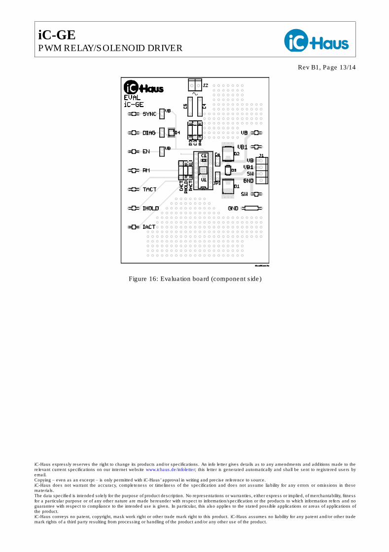
EVALUATION BOARD
iC-GE comes with an evaluation board for test purpose. Figures 15 and 16 show both the schematic and the
component side of the evaluation board.
Figure 15: Schematic of the evaluation board
iC-GEPWM RELAY/SOLENOID DRIVER
Rev B1, Page 13/14
Figure 16: Evaluation board (component side)
iC-Haus expressly reserves the right to change its products and/or specifications. An info letter gives details as to any amendments and additions made to therelevant current specifications on our internet website www.ichaus.de/infoletter; this letter is generated automatically and shall be sent to registered users byemail.Copying – even as an excerpt – is only permitted with iC-Haus’ approval in writing and precise reference to source.iC-Haus does not warrant the accuracy, completeness or timeliness of the specification and does not assume liability for any errors or omissions in thesematerials.The data specified is intended solely for the purpose of product description. No representations or warranties, either express or implied, of merchantability, fitnessfor a particular purpose or of any other nature are made hereunder with respect to information/specification or the products to which information refers and noguarantee with respect to compliance to the intended use is given. In particular, this also applies to the stated possible applications or areas of applications ofthe product.iC-Haus conveys no patent, copyright, mask work right or other trade mark right to this product. iC-Haus assumes no liability for any patent and/or other trademark rights of a third party resulting from processing or handling of the product and/or any other use of the product.

iC-GEPWM RELAY/SOLENOID DRIVER
Rev B1, Page 14/14
ORDERING INFORMATION
Type Package Order Designation
iC-GE QFN16 4 mm x 4 mm iC-GE QFN16-4x4
iC-GE Evaluation Board iC-GE EVAL GE1D
For technical support, information about prices and terms of delivery please contact:
iC-Haus GmbH Tel.: +49 (0) 61 35 - 92 92 - 0
Am Kuemmerling 18 Fax: +49 (0) 61 35 - 92 92 - 192
D-55294 Bodenheim Web: http://www.ichaus.com
GERMANY E-Mail: [email protected]
Appointed local distributors: http://www.ichaus.com/sales_partners
Top Related