


Languages
Pages
Legal

12-Bit AdjustmentFree AD Cs
HS5210 SERIESData Converter Line
FEATURES• 12-bit conversion in 10µS typ; 13µS max• A djustment-free, ±0.0125% linearity• Low power: 670 mW typ• W ide operating temperature range: –55ºC to
+125ºC• Small size: 24-pin, metal-to-metal, hermetic
package• Full M IL-STD-883 Rev. C, Levels B or S, or
commercial processing
DESCRIPTION
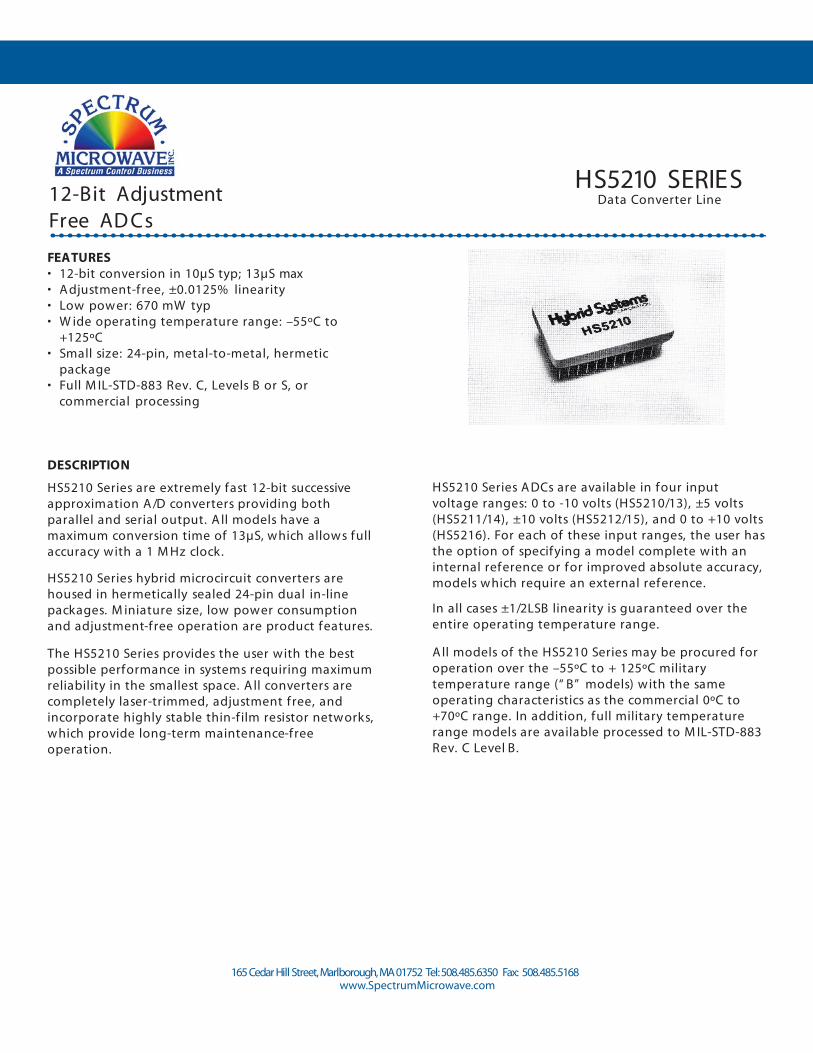
HS5210 Series are extremely fast 12-bit successiveapproximation A /D converters providing bothparallel and serial output. A ll models have amaximum conversion time of 13µS, which allows fullaccuracy with a 1 M Hz clock.
HS5210 Series hybrid microcircuit converters arehoused in hermetically sealed 24-pin dual in-linepackages. M iniature size, low power consumptionand adjustment-free operation are product features.
The HS5210 Series provides the user with the bestpossible performance in systems requiring maximumreliability in the smallest space. A ll converters arecompletely laser-trimmed, adjustment free, andincorporate highly stable thin-f ilm resistor networks,which provide long-term maintenance-freeoperation.
HS5210 Series A DCs are available in four inputvoltage ranges: 0 to -10 volts (HS5210/13), ±5 volts(HS5211/14), ±10 volts (HS5212/15), and 0 to +10 volts(HS5216). For each of these input ranges, the user hasthe option of specifying a model complete with aninternal reference or for improved absolute accuracy,models which require an external reference.
In all cases ±1/2LSB linearity is guaranteed over theentire operating temperature range.
A ll models of the HS5210 Series may be procured foroperation over the –55ºC to + 125ºC militarytemperature range (“ B” models) with the sameoperating characteristics as the commercial 0ºC to+70ºC range. In addition, full military temperaturerange models are available processed to M IL-STD-883Rev. C Level B.
165Cedar Hill Street,Marlborough,MA01752 Tel:508.485.6350 Fax: 508.485.5168www.SpectrumMicrowave.com
SUCCESSIVE APPRO XIMATIO N 12-BIT A/D Converters
A BSOLUTE M A XIM UM RA TINGS:
Operating Temperature –55ºCto+125ºCStorage Temperature –65ºCto+150ºCPositive Supply +18 V oltsNegative Supply –18 V oltsLogic Supply +7 V oltsA nalog Input ±25 V oltsDigital Outputs 0 to Logic SupplyDigital Inputs –0.5 to +5.5 V oltsReference Supply (M odels HS5213. 14, 15) –15 V olts
SPECIFICA TIONS (TA =25º C, V oltages ±15, +5 Unless otherw ise stated)PERFORM A NCE (NOTE 1):
INPUT HIGHINPUT RA NGE IM PEDA NCE PERFORM A NCE HIGH A CCURA CY
(Internal Reference) (Ext. Ref .=–10.000V )0 to-10V 3.6k HS5210 HS5213+5V to -5V 3.6k HS5211 HS5214+10V to-10V 7.2k HS5212 HS52150 to+10V 3.3k HS5216
M A X. M A X. UNITSResolution 12 12 BitsLinearity(25ºC) ±1/2 ±1/2 LSBtM IN to tM A X ±3/4 ±3/4 LSBZero Error 1 1 LSBA bsolute A ccuracy(25ºC)(Note 2) 2 2 LSBA bsolute A ccuracy(–55ºC to +125ºC)(Note 2) ±.4 ±.1 %Conversion Time 13 13 µSecPower Supply RequirmentsCurrent Drain +15 V olt Supply 16 10 mACurrent Drain –1 SV olt Supply 28 28 mACurrent Drain +5V olt Supply (Note 5) 50 50 mACurrent Drain @ Reference Input 2 mAPower Supply Rejection±15 V olts (Note 3) ±1 ±1 LSB/% Supply±5V olts ±1 ±1 LSB/% SupplyPower Consumption 910 825 mW
LOGIC RA TINGSM IN TY P. M A X. UNITS
Input Logic Commands 0.7 V oltsLogic “ 0” 2.0 V oltsLogic “ 1” 0.5 TTL LoadLoading
Clock Input Pulse W idthLogic “ 0” 180 nSecLogic “ 1” 100 nSec
Output LogicLogic “ 0” 0.15 0.4 V oltsLogic “ 1” 2.4 3.6 V oltsSerial OutputParallel Output (See Timing Diagram)Fanout-High 8 TTL LoadFanout-Low 2 TTL Load
LO G IC CO D IN GHS5210/5213 HS5211/5214 HS5212/5215 HS5216 M SB LSB
0.0000V +5.0000V +10.0000V +10.0000V 0000 0000 0000–0.0024V +4.9976V +9.9951V +9.9976V 0000 0000 0000*–4.9976V +0.0024V +0.0049V +5.0024V 0111 1111 1110*–5.0000V 0.0000V 0.0000V +5.0000V 0000 0000 0000*–5.0024V –0.0024V –0.0049V +4.9976V 1000 0000 0000*–9.9976V –4.9976V –9.9951V +0.0024V 1111 1111 1110*
–10.0000V -5.0000V -10.0000V 0.0000V 1111 1111 1111
HS5210 SERIES
(Continued on next page.)
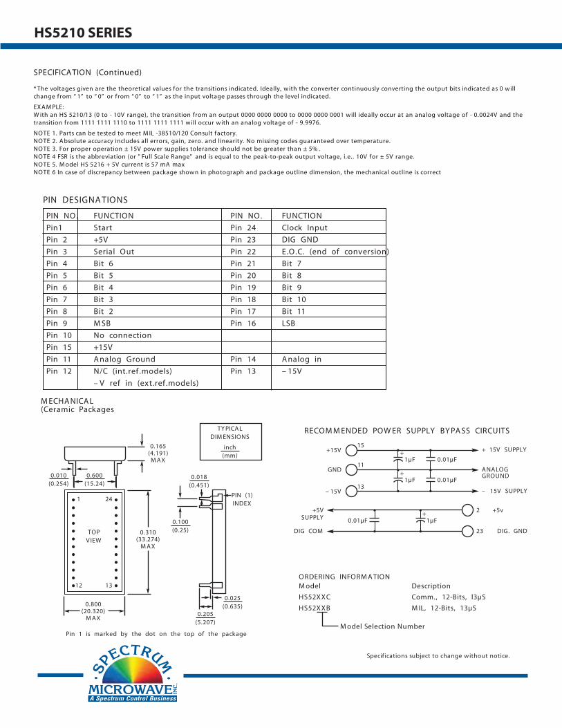
PIN NO. FUNCTION PIN NO. FUNCTION
Pin1 Start Pin 24 Clock Input
Pin 2 +5V Pin 23 DIG GND
Pin 3 Serial Out Pin 22 E.O.C. (end of conversion)
Pin 4 Bit 6 Pin 21 Bit 7
Pin 5 Bit 5 Pin 20 Bit 8
Pin 6 Bit 4 Pin 19 Bit 9
Pin 7 Bit 3 Pin 18 Bit 10
Pin 8 Bit 2 Pin 17 Bit 11
Pin 9 M SB Pin 16 LSB
Pin 10 No connection
Pin 15 +15V
Pin 11 A nalog Ground Pin 14 A nalog in
Pin 12 N/C (int.ref .models) Pin 13 – 15V
– V ref in (ext.ref .models)
ORDERING INFORM A TIONM odel Description
HS52XXC Comm., 12-Bits, l3µS
HS52XXB M IL, 12-Bits, 13µS
M odel Selection Number
Specif ications subject to change without notice.
PIN DESIGNA TIONS
M ECHA NICA L(Ceramic Packages
RECOM M ENDED POW ER SUPPLY BY PA SS CIRCUITS
0.165(4.191)M A X
0.600(15.24)
0.010(0.254)
0.100(0.25)0.310
(33.274)M A X
0.025(0.635)
0.205(5.207)
0.800(20.320)
M A X
0.018(0.451)
PIN (1)INDEX
TOPV IEW
inch(mm)
TY PICA LDIM ENSIONS
241
1312
+15V
GND
– 15V
15
11
13
+5VSUPPLY
DIG COM
0.01µF 1µF+
+1µF
+1µF
0.01µF
0.01µF
+ 15V SUPPLY
– 15V SUPPLY
2 +5v
23 DIG. GND
A NA LOGGROUND
Pin 1 is marked by the dot on the top of the package
SPECIFICA TION (Continued)
* The voltages given are the theoretical values for the transitions indicated. Ideally, with the converter continuously converting the output bits indicated as 0 willchange from “ 1” to “ 0” or from “ 0” to “ 1” as the input voltage passes through the level indicated.
EXA M PLE:W ith an HS 5210/13 (0 to - 10V range), the transition from an output 0000 0000 0000 to 0000 0000 0001 will ideally occur at an analog voltage of - 0.0024V and thetransition from 1111 1111 1110 to 1111 1111 1111 will occur with an analog voltage of - 9.9976.
NOTE 1. Parts can be tested to meet M IL -38510/120 Consult factory.NOTE 2. A bsolute accuracy includes all errors, gain, zero. and linearity. No missing codes guaranteed over temperature.NOTE 3. For proper operation ± 15V power supplies tolerance should not be greater than ± 5% .NOTE 4 FSR is the abbreviation (or " Full Scale Range" and is equal to the peak-to-peak output voltage, i.e.. 10V for ± 5V range.NOTE 5. M odel HS 5216 + 5V current is 57 mA maxNOTE 6 In case of discrepancy between package shown in photograph and package outline dimension, the mechanical outline is correct
HS5210 SERIES
Top Related