


Languages
Pages
Legal

DOCUMENT NUMBERS12CPU15UG/D
HCS12 V1.5 Core
User Guide
Version 1.2
Original Release Date: 12 May 2000Revised: 17 August 2000
Motorola, Inc
Motorola reserves the right to make changes without further notice to any products herein to improve reliability, function ordesign. Motorola does not assume any liability arising out of the application or use of any product or circuit described herein;neither does it convey any license under its patent rights nor the rights of others. Motorola products are not designed, intended,or authorized for use as components in systems intended for surgical implant into the body, or other applications intended tosupport or sustain life, or for any other application in which the failure of the Motorola product could create a situation wherepersonal injury or death may occur. Should Buyer purchase or use Motorola products for any such unintended or unauthorizedapplication, Buyer shall indemnify and hold Motorola and its officers, employees, subsidiaries, affiliates, and distributors harmlessagainst all claims, costs, damages, and expenses, and reasonable attorney fees arising out of, directly or indirectly, any claim ofpersonal injury or death associated with such unintended or unauthorized use, even if such claim alleges that Motorola wasnegligent regarding the design or manufacture of the part.
1
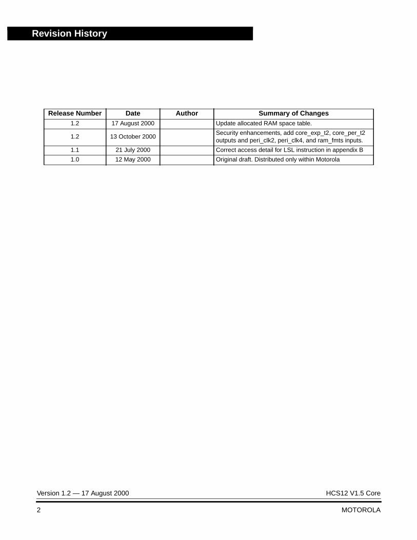
Revision History
Revision History
Release Number Date Author Summary of Changes1.2 17 August 2000 Update allocated RAM space table.
1.2 13 October 2000Security enhancements, add core_exp_t2, core_per_t2outputs and peri_clk2, peri_clk4, and ram_fmts inputs.
1.1 21 July 2000 Correct access detail for LSL instruction in appendix B
1.0 12 May 2000 Original draft. Distributed only within Motorola
Version 1.2 — 17 August 2000 HCS12 V1.5 Core
2 MOTOROLA
Core User Guide — S12CPU15UG V1.2
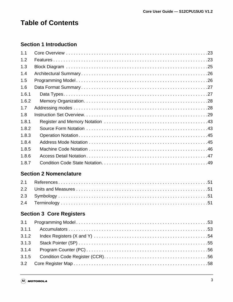
Table of Contents
Section 1 Introduction
1.1 Core Overview . . . . . . . . . . . . . . . . . . . . . . . . . . . . . . . . . . . . . . . . . . . . . . . . . . . . . . . .23
1.2 Features . . . . . . . . . . . . . . . . . . . . . . . . . . . . . . . . . . . . . . . . . . . . . . . . . . . . . . . . . . . . .23
1.3 Block Diagram . . . . . . . . . . . . . . . . . . . . . . . . . . . . . . . . . . . . . . . . . . . . . . . . . . . . . . . .25
1.4 Architectural Summary . . . . . . . . . . . . . . . . . . . . . . . . . . . . . . . . . . . . . . . . . . . . . . . . . .26
1.5 Programming Model . . . . . . . . . . . . . . . . . . . . . . . . . . . . . . . . . . . . . . . . . . . . . . . . . . . .26
1.6 Data Format Summary . . . . . . . . . . . . . . . . . . . . . . . . . . . . . . . . . . . . . . . . . . . . . . . . . .27
1.6.1 Data Types. . . . . . . . . . . . . . . . . . . . . . . . . . . . . . . . . . . . . . . . . . . . . . . . . . . . . . . . .27
1.6.2 Memory Organization. . . . . . . . . . . . . . . . . . . . . . . . . . . . . . . . . . . . . . . . . . . . . . . . .28
1.7 Addressing modes . . . . . . . . . . . . . . . . . . . . . . . . . . . . . . . . . . . . . . . . . . . . . . . . . . . . .28
1.8 Instruction Set Overview. . . . . . . . . . . . . . . . . . . . . . . . . . . . . . . . . . . . . . . . . . . . . . . . .29
1.8.1 Register and Memory Notation . . . . . . . . . . . . . . . . . . . . . . . . . . . . . . . . . . . . . . . . .43
1.8.2 Source Form Notation . . . . . . . . . . . . . . . . . . . . . . . . . . . . . . . . . . . . . . . . . . . . . . . .43
1.8.3 Operation Notation . . . . . . . . . . . . . . . . . . . . . . . . . . . . . . . . . . . . . . . . . . . . . . . . . . .45
1.8.4 Address Mode Notation . . . . . . . . . . . . . . . . . . . . . . . . . . . . . . . . . . . . . . . . . . . . . . .45
1.8.5 Machine Code Notation . . . . . . . . . . . . . . . . . . . . . . . . . . . . . . . . . . . . . . . . . . . . . . .46
1.8.6 Access Detail Notation . . . . . . . . . . . . . . . . . . . . . . . . . . . . . . . . . . . . . . . . . . . . . . . .47
1.8.7 Condition Code State Notation. . . . . . . . . . . . . . . . . . . . . . . . . . . . . . . . . . . . . . . . . .49
Section 2 Nomenclature
2.1 References . . . . . . . . . . . . . . . . . . . . . . . . . . . . . . . . . . . . . . . . . . . . . . . . . . . . . . . . . . .51
2.2 Units and Measures . . . . . . . . . . . . . . . . . . . . . . . . . . . . . . . . . . . . . . . . . . . . . . . . . . . .51
2.3 Symbology . . . . . . . . . . . . . . . . . . . . . . . . . . . . . . . . . . . . . . . . . . . . . . . . . . . . . . . . . . .51
2.4 Terminology . . . . . . . . . . . . . . . . . . . . . . . . . . . . . . . . . . . . . . . . . . . . . . . . . . . . . . . . . .51
Section 3 Core Registers
3.1 Programming Model . . . . . . . . . . . . . . . . . . . . . . . . . . . . . . . . . . . . . . . . . . . . . . . . . . . .53
3.1.1 Accumulators . . . . . . . . . . . . . . . . . . . . . . . . . . . . . . . . . . . . . . . . . . . . . . . . . . . . . . .53
3.1.2 Index Registers (X and Y) . . . . . . . . . . . . . . . . . . . . . . . . . . . . . . . . . . . . . . . . . . . . .54
3.1.3 Stack Pointer (SP) . . . . . . . . . . . . . . . . . . . . . . . . . . . . . . . . . . . . . . . . . . . . . . . . . . .55
3.1.4 Program Counter (PC) . . . . . . . . . . . . . . . . . . . . . . . . . . . . . . . . . . . . . . . . . . . . . . . .56
3.1.5 Condition Code Register (CCR). . . . . . . . . . . . . . . . . . . . . . . . . . . . . . . . . . . . . . . . .56
3.2 Core Register Map . . . . . . . . . . . . . . . . . . . . . . . . . . . . . . . . . . . . . . . . . . . . . . . . . . . . .58
3
Core User Guide — S12CPU15UG V1.2
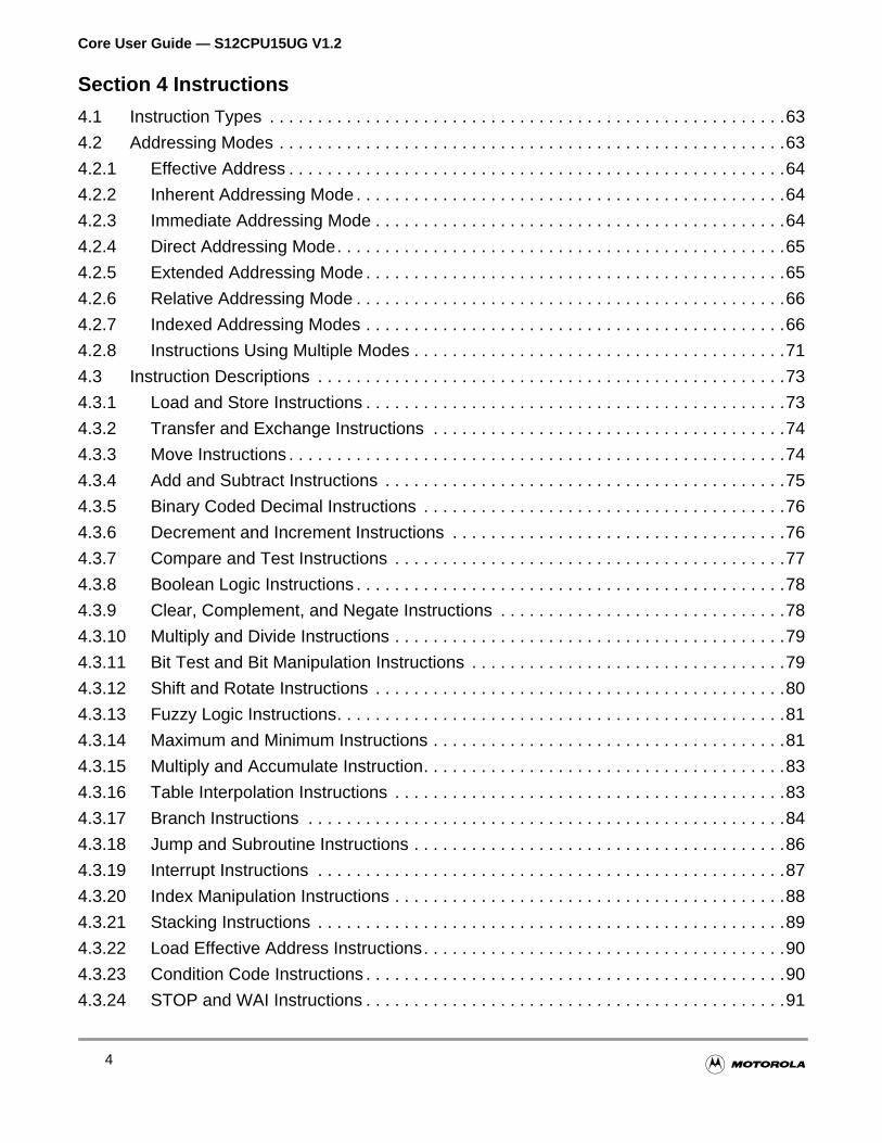
Section 4 Instructions
4.1 Instruction Types . . . . . . . . . . . . . . . . . . . . . . . . . . . . . . . . . . . . . . . . . . . . . . . . . . . . . .63
4.2 Addressing Modes . . . . . . . . . . . . . . . . . . . . . . . . . . . . . . . . . . . . . . . . . . . . . . . . . . . . .63
4.2.1 Effective Address . . . . . . . . . . . . . . . . . . . . . . . . . . . . . . . . . . . . . . . . . . . . . . . . . . . .64
4.2.2 Inherent Addressing Mode . . . . . . . . . . . . . . . . . . . . . . . . . . . . . . . . . . . . . . . . . . . . .64
4.2.3 Immediate Addressing Mode . . . . . . . . . . . . . . . . . . . . . . . . . . . . . . . . . . . . . . . . . . .64
4.2.4 Direct Addressing Mode. . . . . . . . . . . . . . . . . . . . . . . . . . . . . . . . . . . . . . . . . . . . . . .65
4.2.5 Extended Addressing Mode . . . . . . . . . . . . . . . . . . . . . . . . . . . . . . . . . . . . . . . . . . . .65
4.2.6 Relative Addressing Mode . . . . . . . . . . . . . . . . . . . . . . . . . . . . . . . . . . . . . . . . . . . . .66
4.2.7 Indexed Addressing Modes . . . . . . . . . . . . . . . . . . . . . . . . . . . . . . . . . . . . . . . . . . . .66
4.2.8 Instructions Using Multiple Modes . . . . . . . . . . . . . . . . . . . . . . . . . . . . . . . . . . . . . . .71
4.3 Instruction Descriptions . . . . . . . . . . . . . . . . . . . . . . . . . . . . . . . . . . . . . . . . . . . . . . . . .73
4.3.1 Load and Store Instructions . . . . . . . . . . . . . . . . . . . . . . . . . . . . . . . . . . . . . . . . . . . .73
4.3.2 Transfer and Exchange Instructions . . . . . . . . . . . . . . . . . . . . . . . . . . . . . . . . . . . . .74
4.3.3 Move Instructions . . . . . . . . . . . . . . . . . . . . . . . . . . . . . . . . . . . . . . . . . . . . . . . . . . . .74
4.3.4 Add and Subtract Instructions . . . . . . . . . . . . . . . . . . . . . . . . . . . . . . . . . . . . . . . . . .75
4.3.5 Binary Coded Decimal Instructions . . . . . . . . . . . . . . . . . . . . . . . . . . . . . . . . . . . . . .76
4.3.6 Decrement and Increment Instructions . . . . . . . . . . . . . . . . . . . . . . . . . . . . . . . . . . .76
4.3.7 Compare and Test Instructions . . . . . . . . . . . . . . . . . . . . . . . . . . . . . . . . . . . . . . . . .77
4.3.8 Boolean Logic Instructions . . . . . . . . . . . . . . . . . . . . . . . . . . . . . . . . . . . . . . . . . . . . .78
4.3.9 Clear, Complement, and Negate Instructions . . . . . . . . . . . . . . . . . . . . . . . . . . . . . .78
4.3.10 Multiply and Divide Instructions . . . . . . . . . . . . . . . . . . . . . . . . . . . . . . . . . . . . . . . . .79
4.3.11 Bit Test and Bit Manipulation Instructions . . . . . . . . . . . . . . . . . . . . . . . . . . . . . . . . .79
4.3.12 Shift and Rotate Instructions . . . . . . . . . . . . . . . . . . . . . . . . . . . . . . . . . . . . . . . . . . .80
4.3.13 Fuzzy Logic Instructions. . . . . . . . . . . . . . . . . . . . . . . . . . . . . . . . . . . . . . . . . . . . . . .81
4.3.14 Maximum and Minimum Instructions . . . . . . . . . . . . . . . . . . . . . . . . . . . . . . . . . . . . .81
4.3.15 Multiply and Accumulate Instruction. . . . . . . . . . . . . . . . . . . . . . . . . . . . . . . . . . . . . .83
4.3.16 Table Interpolation Instructions . . . . . . . . . . . . . . . . . . . . . . . . . . . . . . . . . . . . . . . . .83
4.3.17 Branch Instructions . . . . . . . . . . . . . . . . . . . . . . . . . . . . . . . . . . . . . . . . . . . . . . . . . .84
4.3.18 Jump and Subroutine Instructions . . . . . . . . . . . . . . . . . . . . . . . . . . . . . . . . . . . . . . .86
4.3.19 Interrupt Instructions . . . . . . . . . . . . . . . . . . . . . . . . . . . . . . . . . . . . . . . . . . . . . . . . .87
4.3.20 Index Manipulation Instructions . . . . . . . . . . . . . . . . . . . . . . . . . . . . . . . . . . . . . . . . .88
4.3.21 Stacking Instructions . . . . . . . . . . . . . . . . . . . . . . . . . . . . . . . . . . . . . . . . . . . . . . . . .89
4.3.22 Load Effective Address Instructions. . . . . . . . . . . . . . . . . . . . . . . . . . . . . . . . . . . . . .90
4.3.23 Condition Code Instructions . . . . . . . . . . . . . . . . . . . . . . . . . . . . . . . . . . . . . . . . . . . .90
4.3.24 STOP and WAI Instructions . . . . . . . . . . . . . . . . . . . . . . . . . . . . . . . . . . . . . . . . . . . .91
4
Core User Guide — S12CPU15UG V1.2
4.3.25 Background Mode and Null Operation Instructions . . . . . . . . . . . . . . . . . . . . . . . . . .91
4.4 High-Level Language Support . . . . . . . . . . . . . . . . . . . . . . . . . . . . . . . . . . . . . . . . . . . .92
4.4.1 Data Types. . . . . . . . . . . . . . . . . . . . . . . . . . . . . . . . . . . . . . . . . . . . . . . . . . . . . . . . .92
4.4.2 Parameters and Variables . . . . . . . . . . . . . . . . . . . . . . . . . . . . . . . . . . . . . . . . . . . . .92
4.4.3 Increment and Decrement Operators. . . . . . . . . . . . . . . . . . . . . . . . . . . . . . . . . . . . .94
4.4.4 Higher Math Functions . . . . . . . . . . . . . . . . . . . . . . . . . . . . . . . . . . . . . . . . . . . . . . . .94
4.4.5 Conditional If Constructs . . . . . . . . . . . . . . . . . . . . . . . . . . . . . . . . . . . . . . . . . . . . . .94
4.4.6 Case and Switch Statements . . . . . . . . . . . . . . . . . . . . . . . . . . . . . . . . . . . . . . . . . . .95
4.4.7 Pointers . . . . . . . . . . . . . . . . . . . . . . . . . . . . . . . . . . . . . . . . . . . . . . . . . . . . . . . . . . .95
4.4.8 Function Calls . . . . . . . . . . . . . . . . . . . . . . . . . . . . . . . . . . . . . . . . . . . . . . . . . . . . . .95
4.4.9 Instruction Set Orthogonality . . . . . . . . . . . . . . . . . . . . . . . . . . . . . . . . . . . . . . . . . . .95
4.5 Opcode Map. . . . . . . . . . . . . . . . . . . . . . . . . . . . . . . . . . . . . . . . . . . . . . . . . . . . . . . . . .97
4.6 Transfer and Exchange Postbyte Encoding . . . . . . . . . . . . . . . . . . . . . . . . . . . . . . . . . .99
4.7 Loop Primitive Postbyte (lb) Encoding . . . . . . . . . . . . . . . . . . . . . . . . . . . . . . . . . . . . .100
4.8 Indexed Addressing Postbyte (xb) Encoding . . . . . . . . . . . . . . . . . . . . . . . . . . . . . . . .101
Section 5 Instruction Execution
5.1 Normal Instruction Execution . . . . . . . . . . . . . . . . . . . . . . . . . . . . . . . . . . . . . . . . . . . .103
5.2 Execution Sequence. . . . . . . . . . . . . . . . . . . . . . . . . . . . . . . . . . . . . . . . . . . . . . . . . . .103
5.2.1 No Movement. . . . . . . . . . . . . . . . . . . . . . . . . . . . . . . . . . . . . . . . . . . . . . . . . . . . . .103
5.2.2 Advance and Load from Data Bus . . . . . . . . . . . . . . . . . . . . . . . . . . . . . . . . . . . . . .103
5.3 Changes of Flow. . . . . . . . . . . . . . . . . . . . . . . . . . . . . . . . . . . . . . . . . . . . . . . . . . . . . .104
5.3.1 Exceptions . . . . . . . . . . . . . . . . . . . . . . . . . . . . . . . . . . . . . . . . . . . . . . . . . . . . . . . .104
5.3.2 Subroutines . . . . . . . . . . . . . . . . . . . . . . . . . . . . . . . . . . . . . . . . . . . . . . . . . . . . . . .104
5.3.3 Branches . . . . . . . . . . . . . . . . . . . . . . . . . . . . . . . . . . . . . . . . . . . . . . . . . . . . . . . . .104
5.3.4 Jumps. . . . . . . . . . . . . . . . . . . . . . . . . . . . . . . . . . . . . . . . . . . . . . . . . . . . . . . . . . . .106
5.4 Instruction Timing . . . . . . . . . . . . . . . . . . . . . . . . . . . . . . . . . . . . . . . . . . . . . . . . . . . . .106
5.4.1 Register and Memory Notation . . . . . . . . . . . . . . . . . . . . . . . . . . . . . . . . . . . . . . . .120
5.4.2 Source Form Notation . . . . . . . . . . . . . . . . . . . . . . . . . . . . . . . . . . . . . . . . . . . . . . .121
5.4.3 Operation Notation . . . . . . . . . . . . . . . . . . . . . . . . . . . . . . . . . . . . . . . . . . . . . . . . . .122
5.4.4 Address Mode Notation . . . . . . . . . . . . . . . . . . . . . . . . . . . . . . . . . . . . . . . . . . . . . .122
5.4.5 Machine Code Notation . . . . . . . . . . . . . . . . . . . . . . . . . . . . . . . . . . . . . . . . . . . . . .123
5.4.6 Access Detail Notation . . . . . . . . . . . . . . . . . . . . . . . . . . . . . . . . . . . . . . . . . . . . . . .123
5.4.7 Condition Code State Notation. . . . . . . . . . . . . . . . . . . . . . . . . . . . . . . . . . . . . . . . .126
5.5 External Visibility Of Instruction Queue . . . . . . . . . . . . . . . . . . . . . . . . . . . . . . . . . . . .126
5.5.1 Instruction Queue Status Signals. . . . . . . . . . . . . . . . . . . . . . . . . . . . . . . . . . . . . . .126
5
Core User Guide — S12CPU15UG V1.2
5.5.2 No Movement (0:0) . . . . . . . . . . . . . . . . . . . . . . . . . . . . . . . . . . . . . . . . . . . . . . . . .128
5.5.3 ALD — Advance and Load from Data Bus (1:0) . . . . . . . . . . . . . . . . . . . . . . . . . . .128
5.5.4 INT — Start Interrupt (0:1) . . . . . . . . . . . . . . . . . . . . . . . . . . . . . . . . . . . . . . . . . . . .128
5.5.5 SEV — Start Even Instruction (1:0) . . . . . . . . . . . . . . . . . . . . . . . . . . . . . . . . . . . . .128
5.5.6 SOD — Start Odd Instruction (1:1) . . . . . . . . . . . . . . . . . . . . . . . . . . . . . . . . . . . . .129
Section 6 Exception Processing
6.1 Exception Processing Overview. . . . . . . . . . . . . . . . . . . . . . . . . . . . . . . . . . . . . . . . . .131
6.1.1 Reset Processing . . . . . . . . . . . . . . . . . . . . . . . . . . . . . . . . . . . . . . . . . . . . . . . . . . .133
6.1.2 Interrupt Processing . . . . . . . . . . . . . . . . . . . . . . . . . . . . . . . . . . . . . . . . . . . . . . . . .133
6.2 Exception Vectors. . . . . . . . . . . . . . . . . . . . . . . . . . . . . . . . . . . . . . . . . . . . . . . . . . . . .135
6.3 Exception Types. . . . . . . . . . . . . . . . . . . . . . . . . . . . . . . . . . . . . . . . . . . . . . . . . . . . . .136
6.3.1 Resets . . . . . . . . . . . . . . . . . . . . . . . . . . . . . . . . . . . . . . . . . . . . . . . . . . . . . . . . . . .136
6.3.2 Interrupts . . . . . . . . . . . . . . . . . . . . . . . . . . . . . . . . . . . . . . . . . . . . . . . . . . . . . . . . .137
Section 7 Core Interface
7.1 Core Interface Overview. . . . . . . . . . . . . . . . . . . . . . . . . . . . . . . . . . . . . . . . . . . . . . . .141
7.1.1 Signal Summary. . . . . . . . . . . . . . . . . . . . . . . . . . . . . . . . . . . . . . . . . . . . . . . . . . . .142
7.2 Signal Descriptions. . . . . . . . . . . . . . . . . . . . . . . . . . . . . . . . . . . . . . . . . . . . . . . . . . . .145
7.2.1 Internal Bus Interface Signals . . . . . . . . . . . . . . . . . . . . . . . . . . . . . . . . . . . . . . . . .145
7.2.2 External Bus Interface Signals . . . . . . . . . . . . . . . . . . . . . . . . . . . . . . . . . . . . . . . . .148
7.2.3 Clock and Reset Signals . . . . . . . . . . . . . . . . . . . . . . . . . . . . . . . . . . . . . . . . . . . . .150
7.2.4 Vector Request/Acknowledge Signals . . . . . . . . . . . . . . . . . . . . . . . . . . . . . . . . . . .151
7.2.5 Stop and Wait Mode Control/Status Signals . . . . . . . . . . . . . . . . . . . . . . . . . . . . . .151
7.2.6 Background Debug Mode (BDM) Interface Signals . . . . . . . . . . . . . . . . . . . . . . . . .151
7.2.7 Memory Configuration Signals . . . . . . . . . . . . . . . . . . . . . . . . . . . . . . . . . . . . . . . . .152
7.2.8 Scan Control Interface Signals. . . . . . . . . . . . . . . . . . . . . . . . . . . . . . . . . . . . . . . . .152
7.3 Interface Operation. . . . . . . . . . . . . . . . . . . . . . . . . . . . . . . . . . . . . . . . . . . . . . . . . . . .152
7.3.1 Read Operations . . . . . . . . . . . . . . . . . . . . . . . . . . . . . . . . . . . . . . . . . . . . . . . . . . .152
7.3.2 Write Operations . . . . . . . . . . . . . . . . . . . . . . . . . . . . . . . . . . . . . . . . . . . . . . . . . . .155
7.3.3 Multiplexed External Bus Interface. . . . . . . . . . . . . . . . . . . . . . . . . . . . . . . . . . . . . .158
7.3.4 General Internal Read Visibility Timing . . . . . . . . . . . . . . . . . . . . . . . . . . . . . . . . . .161
7.3.5 Detecting Access Type from External Signals . . . . . . . . . . . . . . . . . . . . . . . . . . . . .162
Section 8 Core Clock and Reset Connections
8.1 Clocking Overview . . . . . . . . . . . . . . . . . . . . . . . . . . . . . . . . . . . . . . . . . . . . . . . . . . . .163
6
Core User Guide — S12CPU15UG V1.2
8.1.1 Basic Clock Relationship . . . . . . . . . . . . . . . . . . . . . . . . . . . . . . . . . . . . . . . . . . . . .164
8.1.2 Reset Relationship . . . . . . . . . . . . . . . . . . . . . . . . . . . . . . . . . . . . . . . . . . . . . . . . . .165
8.1.3 Phase-Locked Loop Interface . . . . . . . . . . . . . . . . . . . . . . . . . . . . . . . . . . . . . . . . .165
8.1.4 HCS12 CPU Wait and Stop Modes . . . . . . . . . . . . . . . . . . . . . . . . . . . . . . . . . . . . .166
8.2 Signal Summary . . . . . . . . . . . . . . . . . . . . . . . . . . . . . . . . . . . . . . . . . . . . . . . . . . . . . .166
8.3 Detailed Clock and Reset Signal Descriptions . . . . . . . . . . . . . . . . . . . . . . . . . . . . . . .167
8.3.1 Clock and Reset Signals . . . . . . . . . . . . . . . . . . . . . . . . . . . . . . . . . . . . . . . . . . . . .167
8.3.2 Stop and Wait Mode Control/Status Signals . . . . . . . . . . . . . . . . . . . . . . . . . . . . . .168
Section 9 Core Power Connections
9.1 Power Overview . . . . . . . . . . . . . . . . . . . . . . . . . . . . . . . . . . . . . . . . . . . . . . . . . . . . . .169
9.1.1 Power and Ground Summary. . . . . . . . . . . . . . . . . . . . . . . . . . . . . . . . . . . . . . . . . .169
Section 10 Interrupt (INT)
10.1 Overview. . . . . . . . . . . . . . . . . . . . . . . . . . . . . . . . . . . . . . . . . . . . . . . . . . . . . . . . . . . .171
10.1.1 Features . . . . . . . . . . . . . . . . . . . . . . . . . . . . . . . . . . . . . . . . . . . . . . . . . . . . . . . . . .171
10.1.2 Block Diagram . . . . . . . . . . . . . . . . . . . . . . . . . . . . . . . . . . . . . . . . . . . . . . . . . . . . .172
10.2 Interface Signals. . . . . . . . . . . . . . . . . . . . . . . . . . . . . . . . . . . . . . . . . . . . . . . . . . . . . .172
10.3 Registers . . . . . . . . . . . . . . . . . . . . . . . . . . . . . . . . . . . . . . . . . . . . . . . . . . . . . . . . . . .173
10.3.1 Interrupt Test Control Register. . . . . . . . . . . . . . . . . . . . . . . . . . . . . . . . . . . . . . . . .173
10.3.2 Interrupt Test Registers . . . . . . . . . . . . . . . . . . . . . . . . . . . . . . . . . . . . . . . . . . . . . .174
10.3.3 Highest Priority I Interrupt (Optional) . . . . . . . . . . . . . . . . . . . . . . . . . . . . . . . . . . . .175
10.4 Operation . . . . . . . . . . . . . . . . . . . . . . . . . . . . . . . . . . . . . . . . . . . . . . . . . . . . . . . . . . .175
10.4.1 Interrupt Exception Requests. . . . . . . . . . . . . . . . . . . . . . . . . . . . . . . . . . . . . . . . . .175
10.4.2 Reset Exception Requests. . . . . . . . . . . . . . . . . . . . . . . . . . . . . . . . . . . . . . . . . . . .176
10.4.3 Exception Priority . . . . . . . . . . . . . . . . . . . . . . . . . . . . . . . . . . . . . . . . . . . . . . . . . . .176
10.5 Modes of Operation . . . . . . . . . . . . . . . . . . . . . . . . . . . . . . . . . . . . . . . . . . . . . . . . . . .177
10.5.1 Normal Operation. . . . . . . . . . . . . . . . . . . . . . . . . . . . . . . . . . . . . . . . . . . . . . . . . . .177
10.5.2 Special Operation. . . . . . . . . . . . . . . . . . . . . . . . . . . . . . . . . . . . . . . . . . . . . . . . . . .177
10.5.3 Emulation Modes . . . . . . . . . . . . . . . . . . . . . . . . . . . . . . . . . . . . . . . . . . . . . . . . . . .177
10.6 Low-Power Options . . . . . . . . . . . . . . . . . . . . . . . . . . . . . . . . . . . . . . . . . . . . . . . . . . .177
10.6.1 Run Mode. . . . . . . . . . . . . . . . . . . . . . . . . . . . . . . . . . . . . . . . . . . . . . . . . . . . . . . . .177
10.6.2 Wait Mode . . . . . . . . . . . . . . . . . . . . . . . . . . . . . . . . . . . . . . . . . . . . . . . . . . . . . . . .177
10.6.3 Stop Mode . . . . . . . . . . . . . . . . . . . . . . . . . . . . . . . . . . . . . . . . . . . . . . . . . . . . . . . .177
10.7 Motorola Internal Information . . . . . . . . . . . . . . . . . . . . . . . . . . . . . . . . . . . . . . . . . . . .177
Section 11 Module Mapping Control (MMC)
7
Core User Guide — S12CPU15UG V1.2
11.1 Overview. . . . . . . . . . . . . . . . . . . . . . . . . . . . . . . . . . . . . . . . . . . . . . . . . . . . . . . . . . . .179
11.1.1 Features . . . . . . . . . . . . . . . . . . . . . . . . . . . . . . . . . . . . . . . . . . . . . . . . . . . . . . . . . .179
11.1.2 Block Diagram . . . . . . . . . . . . . . . . . . . . . . . . . . . . . . . . . . . . . . . . . . . . . . . . . . . . .180
11.2 Interface Signals. . . . . . . . . . . . . . . . . . . . . . . . . . . . . . . . . . . . . . . . . . . . . . . . . . . . . .180
11.3 Registers . . . . . . . . . . . . . . . . . . . . . . . . . . . . . . . . . . . . . . . . . . . . . . . . . . . . . . . . . . .181
11.3.1 Initialization of Internal RAM Position Register (INITRM) . . . . . . . . . . . . . . . . . . . .182
11.3.2 Initialization of Internal Registers Position Register (INITRG) . . . . . . . . . . . . . . . . .182
11.3.3 Initialization of Internal EEPROM Position Register (INITEE) . . . . . . . . . . . . . . . . .183
11.3.4 Miscellaneous System Control Register (MISC) . . . . . . . . . . . . . . . . . . . . . . . . . . .184
11.3.5 Reserved Test Register Zero (MTST0) . . . . . . . . . . . . . . . . . . . . . . . . . . . . . . . . . .185
11.3.6 Reserved Test Register One (MTST1) . . . . . . . . . . . . . . . . . . . . . . . . . . . . . . . . . .185
11.3.7 Memory Size Register Zero (MEMSIZ0) . . . . . . . . . . . . . . . . . . . . . . . . . . . . . . . . .186
11.3.8 Memory Size Register One (MEMSIZ1). . . . . . . . . . . . . . . . . . . . . . . . . . . . . . . . . .187
11.3.9 Program Page Index Register (PPAGE) . . . . . . . . . . . . . . . . . . . . . . . . . . . . . . . . .188
11.4 Operation . . . . . . . . . . . . . . . . . . . . . . . . . . . . . . . . . . . . . . . . . . . . . . . . . . . . . . . . . . .189
11.4.1 Bus Control . . . . . . . . . . . . . . . . . . . . . . . . . . . . . . . . . . . . . . . . . . . . . . . . . . . . . . .189
11.4.2 Address Decoding . . . . . . . . . . . . . . . . . . . . . . . . . . . . . . . . . . . . . . . . . . . . . . . . . .189
11.4.3 Memory Expansion . . . . . . . . . . . . . . . . . . . . . . . . . . . . . . . . . . . . . . . . . . . . . . . . .191
11.5 Motorola Internal Information . . . . . . . . . . . . . . . . . . . . . . . . . . . . . . . . . . . . . . . . . . . .196
11.5.1 Test Registers . . . . . . . . . . . . . . . . . . . . . . . . . . . . . . . . . . . . . . . . . . . . . . . . . . . . .196
11.5.2 MMC Bus Control. . . . . . . . . . . . . . . . . . . . . . . . . . . . . . . . . . . . . . . . . . . . . . . . . . .198
Section 12 Multiplexed External Bus Interface (MEBI)
12.1 Overview. . . . . . . . . . . . . . . . . . . . . . . . . . . . . . . . . . . . . . . . . . . . . . . . . . . . . . . . . . . .201
12.1.1 Features . . . . . . . . . . . . . . . . . . . . . . . . . . . . . . . . . . . . . . . . . . . . . . . . . . . . . . . . . .201
12.1.2 Block Diagram . . . . . . . . . . . . . . . . . . . . . . . . . . . . . . . . . . . . . . . . . . . . . . . . . . . . .202
12.2 Interface Signals. . . . . . . . . . . . . . . . . . . . . . . . . . . . . . . . . . . . . . . . . . . . . . . . . . . . . .202
12.2.1 MEBI Signal Descriptions. . . . . . . . . . . . . . . . . . . . . . . . . . . . . . . . . . . . . . . . . . . . .203
12.3 Registers . . . . . . . . . . . . . . . . . . . . . . . . . . . . . . . . . . . . . . . . . . . . . . . . . . . . . . . . . . .207
12.3.1 Port A Data Register (PORTA) . . . . . . . . . . . . . . . . . . . . . . . . . . . . . . . . . . . . . . . .208
12.3.2 Data Direction Register A (DDRA) . . . . . . . . . . . . . . . . . . . . . . . . . . . . . . . . . . . . . .209
12.3.3 Port B Data Register (PORTB) . . . . . . . . . . . . . . . . . . . . . . . . . . . . . . . . . . . . . . . .210
12.3.4 Data Direction Register B (DDRB) . . . . . . . . . . . . . . . . . . . . . . . . . . . . . . . . . . . . . .210
12.3.5 Port E Data Register (PORTE) . . . . . . . . . . . . . . . . . . . . . . . . . . . . . . . . . . . . . . . .211
12.3.6 Data Direction Register E (DDRE) . . . . . . . . . . . . . . . . . . . . . . . . . . . . . . . . . . . . . .212
12.3.7 Port E Assignment Register (PEAR) . . . . . . . . . . . . . . . . . . . . . . . . . . . . . . . . . . . .213
8
Core User Guide — S12CPU15UG V1.2
12.3.8 MODE Register (MODE) . . . . . . . . . . . . . . . . . . . . . . . . . . . . . . . . . . . . . . . . . . . . .215
12.3.9 Pullup Control Register (PUCR). . . . . . . . . . . . . . . . . . . . . . . . . . . . . . . . . . . . . . . .218
12.3.10 Reduced Drive Register (RDRIV) . . . . . . . . . . . . . . . . . . . . . . . . . . . . . . . . . . . . . .219
12.3.11 External Bus Interface Control Register (EBICTL). . . . . . . . . . . . . . . . . . . . . . . . . .220
12.3.12 IRQ Control Register (IRQCR). . . . . . . . . . . . . . . . . . . . . . . . . . . . . . . . . . . . . . . . .220
12.3.13 Reserved Registers.. . . . . . . . . . . . . . . . . . . . . . . . . . . . . . . . . . . . . . . . . . . . . . . . .222
12.3.14 Port K Data Register (PORTK). . . . . . . . . . . . . . . . . . . . . . . . . . . . . . . . . . . . . . . . .222
12.3.15 Port K Data Direction Register (DDRK) . . . . . . . . . . . . . . . . . . . . . . . . . . . . . . . . . .223
12.4 Operation . . . . . . . . . . . . . . . . . . . . . . . . . . . . . . . . . . . . . . . . . . . . . . . . . . . . . . . . . . .224
12.4.1 External Bus Control . . . . . . . . . . . . . . . . . . . . . . . . . . . . . . . . . . . . . . . . . . . . . . . .224
12.4.2 External Data Bus Interface . . . . . . . . . . . . . . . . . . . . . . . . . . . . . . . . . . . . . . . . . . .224
12.4.3 Control . . . . . . . . . . . . . . . . . . . . . . . . . . . . . . . . . . . . . . . . . . . . . . . . . . . . . . . . . . .224
12.4.4 Registers . . . . . . . . . . . . . . . . . . . . . . . . . . . . . . . . . . . . . . . . . . . . . . . . . . . . . . . . .224
12.4.5 External System Pin Functional Descriptions . . . . . . . . . . . . . . . . . . . . . . . . . . . . .225
12.4.6 Detecting Access Type from External Signals . . . . . . . . . . . . . . . . . . . . . . . . . . . . .226
12.4.7 Stretched Bus Cycles. . . . . . . . . . . . . . . . . . . . . . . . . . . . . . . . . . . . . . . . . . . . . . . .227
12.4.8 Modes of Operation . . . . . . . . . . . . . . . . . . . . . . . . . . . . . . . . . . . . . . . . . . . . . . . . .227
12.4.9 Internal Visibility . . . . . . . . . . . . . . . . . . . . . . . . . . . . . . . . . . . . . . . . . . . . . . . . . . . .231
12.4.10 Secure Mode . . . . . . . . . . . . . . . . . . . . . . . . . . . . . . . . . . . . . . . . . . . . . . . . . . . . . .232
12.5 Low-Power Options . . . . . . . . . . . . . . . . . . . . . . . . . . . . . . . . . . . . . . . . . . . . . . . . . . .232
12.5.1 Run Mode. . . . . . . . . . . . . . . . . . . . . . . . . . . . . . . . . . . . . . . . . . . . . . . . . . . . . . . . .232
12.5.2 Wait Mode . . . . . . . . . . . . . . . . . . . . . . . . . . . . . . . . . . . . . . . . . . . . . . . . . . . . . . . .232
12.5.3 Stop Mode . . . . . . . . . . . . . . . . . . . . . . . . . . . . . . . . . . . . . . . . . . . . . . . . . . . . . . . .232
12.6 Motorola Internal Information . . . . . . . . . . . . . . . . . . . . . . . . . . . . . . . . . . . . . . . . . . . .232
12.6.1 Peripheral Mode Operation . . . . . . . . . . . . . . . . . . . . . . . . . . . . . . . . . . . . . . . . . . .232
12.6.2 Special Test Clock . . . . . . . . . . . . . . . . . . . . . . . . . . . . . . . . . . . . . . . . . . . . . . . . . .233
Section 13 Breakpoint (BKP)
13.1 Overview. . . . . . . . . . . . . . . . . . . . . . . . . . . . . . . . . . . . . . . . . . . . . . . . . . . . . . . . . . . .235
13.1.1 Features . . . . . . . . . . . . . . . . . . . . . . . . . . . . . . . . . . . . . . . . . . . . . . . . . . . . . . . . . .235
13.1.2 Block Diagram . . . . . . . . . . . . . . . . . . . . . . . . . . . . . . . . . . . . . . . . . . . . . . . . . . . . .236
13.2 Interface Signals. . . . . . . . . . . . . . . . . . . . . . . . . . . . . . . . . . . . . . . . . . . . . . . . . . . . . .238
13.3 Registers . . . . . . . . . . . . . . . . . . . . . . . . . . . . . . . . . . . . . . . . . . . . . . . . . . . . . . . . . . .238
13.3.1 Breakpoint Control Register 0 (BKPCT0). . . . . . . . . . . . . . . . . . . . . . . . . . . . . . . . .238
13.3.2 Breakpoint Control Register 1 (BKPCT1). . . . . . . . . . . . . . . . . . . . . . . . . . . . . . . . .239
13.3.3 Breakpoint First Address Expansion Register (BKP0X). . . . . . . . . . . . . . . . . . . . . .242
9
Core User Guide — S12CPU15UG V1.2
13.3.4 Breakpoint First Address High Byte Register (BKP0H) . . . . . . . . . . . . . . . . . . . . . .243
13.3.5 Breakpoint First Address Low Byte Register (BKP0L) . . . . . . . . . . . . . . . . . . . . . . .243
13.3.6 Breakpoint Second Address Expansion Register (BKP1X) . . . . . . . . . . . . . . . . . . .243
13.3.7 Breakpoint Data (Second Address) High Byte Register (BKP1H) . . . . . . . . . . . . . .244
13.3.8 Breakpoint Data (Second Address) Low Byte Register (BKP1L). . . . . . . . . . . . . . .244
13.4 Operation . . . . . . . . . . . . . . . . . . . . . . . . . . . . . . . . . . . . . . . . . . . . . . . . . . . . . . . . . . .245
13.4.1 Modes of Operation . . . . . . . . . . . . . . . . . . . . . . . . . . . . . . . . . . . . . . . . . . . . . . . . .245
13.4.2 Breakpoint Priority . . . . . . . . . . . . . . . . . . . . . . . . . . . . . . . . . . . . . . . . . . . . . . . . . .246
13.5 Motorola Internal Information . . . . . . . . . . . . . . . . . . . . . . . . . . . . . . . . . . . . . . . . . . . .246
Section 14 Background Debug Mode (BDM)
14.1 Overview. . . . . . . . . . . . . . . . . . . . . . . . . . . . . . . . . . . . . . . . . . . . . . . . . . . . . . . . . . . .247
14.1.1 Features . . . . . . . . . . . . . . . . . . . . . . . . . . . . . . . . . . . . . . . . . . . . . . . . . . . . . . . . . .247
14.1.2 Block Diagram . . . . . . . . . . . . . . . . . . . . . . . . . . . . . . . . . . . . . . . . . . . . . . . . . . . . .248
14.2 Interface Signals. . . . . . . . . . . . . . . . . . . . . . . . . . . . . . . . . . . . . . . . . . . . . . . . . . . . . .248
14.2.1 Background Interface Pin (BKGD) . . . . . . . . . . . . . . . . . . . . . . . . . . . . . . . . . . . . . .248
14.2.2 High Byte Instruction Tagging Pin (TAGHI) . . . . . . . . . . . . . . . . . . . . . . . . . . . . . . .248
14.2.3 Low Byte Instruction Tagging Pin (TAGLO) . . . . . . . . . . . . . . . . . . . . . . . . . . . . . . .249
14.3 Registers . . . . . . . . . . . . . . . . . . . . . . . . . . . . . . . . . . . . . . . . . . . . . . . . . . . . . . . . . . .249
14.3.1 BDM Status Register . . . . . . . . . . . . . . . . . . . . . . . . . . . . . . . . . . . . . . . . . . . . . . . .250
14.3.2 BDM CCR Holding Register . . . . . . . . . . . . . . . . . . . . . . . . . . . . . . . . . . . . . . . . . .252
14.3.3 BDM Internal Register Position Register . . . . . . . . . . . . . . . . . . . . . . . . . . . . . . . . .253
14.4 Operation . . . . . . . . . . . . . . . . . . . . . . . . . . . . . . . . . . . . . . . . . . . . . . . . . . . . . . . . . . .253
14.4.1 Security . . . . . . . . . . . . . . . . . . . . . . . . . . . . . . . . . . . . . . . . . . . . . . . . . . . . . . . . . .253
14.4.2 Enabling and Activating BDM. . . . . . . . . . . . . . . . . . . . . . . . . . . . . . . . . . . . . . . . . .254
14.4.3 BDM Hardware Commands . . . . . . . . . . . . . . . . . . . . . . . . . . . . . . . . . . . . . . . . . . .254
14.4.4 Standard BDM Firmware Commands . . . . . . . . . . . . . . . . . . . . . . . . . . . . . . . . . . .255
14.4.5 BDM Command Structure . . . . . . . . . . . . . . . . . . . . . . . . . . . . . . . . . . . . . . . . . . . .256
14.4.6 BDM Serial Interface . . . . . . . . . . . . . . . . . . . . . . . . . . . . . . . . . . . . . . . . . . . . . . . .258
14.4.7 Instruction Tracing . . . . . . . . . . . . . . . . . . . . . . . . . . . . . . . . . . . . . . . . . . . . . . . . . .260
14.4.8 Instruction Tagging. . . . . . . . . . . . . . . . . . . . . . . . . . . . . . . . . . . . . . . . . . . . . . . . . .260
14.5 Modes of Operation . . . . . . . . . . . . . . . . . . . . . . . . . . . . . . . . . . . . . . . . . . . . . . . . . . .261
14.5.1 Normal Operation. . . . . . . . . . . . . . . . . . . . . . . . . . . . . . . . . . . . . . . . . . . . . . . . . . .261
14.5.2 Special Operation. . . . . . . . . . . . . . . . . . . . . . . . . . . . . . . . . . . . . . . . . . . . . . . . . . .262
14.5.3 Emulation Modes . . . . . . . . . . . . . . . . . . . . . . . . . . . . . . . . . . . . . . . . . . . . . . . . . . .262
14.6 Low-Power Options . . . . . . . . . . . . . . . . . . . . . . . . . . . . . . . . . . . . . . . . . . . . . . . . . . .262
10
Core User Guide — S12CPU15UG V1.2
14.6.1 Run Mode. . . . . . . . . . . . . . . . . . . . . . . . . . . . . . . . . . . . . . . . . . . . . . . . . . . . . . . . .262
14.6.2 Wait Mode . . . . . . . . . . . . . . . . . . . . . . . . . . . . . . . . . . . . . . . . . . . . . . . . . . . . . . . .262
14.6.3 Stop Mode . . . . . . . . . . . . . . . . . . . . . . . . . . . . . . . . . . . . . . . . . . . . . . . . . . . . . . . .262
14.7 Interrupt Operation . . . . . . . . . . . . . . . . . . . . . . . . . . . . . . . . . . . . . . . . . . . . . . . . . . . .262
14.8 Motorola Internal Information . . . . . . . . . . . . . . . . . . . . . . . . . . . . . . . . . . . . . . . . . . . .262
14.8.1 Registers . . . . . . . . . . . . . . . . . . . . . . . . . . . . . . . . . . . . . . . . . . . . . . . . . . . . . . . . .263
14.8.2 BDM Instruction Register (Hardware) . . . . . . . . . . . . . . . . . . . . . . . . . . . . . . . . . . .264
14.8.3 BDM Instruction Register (Firmware) . . . . . . . . . . . . . . . . . . . . . . . . . . . . . . . . . . .265
14.8.4 BDM Status Register . . . . . . . . . . . . . . . . . . . . . . . . . . . . . . . . . . . . . . . . . . . . . . . .266
14.8.5 BDM Shift Register . . . . . . . . . . . . . . . . . . . . . . . . . . . . . . . . . . . . . . . . . . . . . . . . .267
14.8.6 BDM Address Register . . . . . . . . . . . . . . . . . . . . . . . . . . . . . . . . . . . . . . . . . . . . . .268
14.8.7 Special Peripheral Mode . . . . . . . . . . . . . . . . . . . . . . . . . . . . . . . . . . . . . . . . . . . . .268
14.8.8 Standard BDM Firmware Listing . . . . . . . . . . . . . . . . . . . . . . . . . . . . . . . . . . . . . . .268
14.8.9 Secured Mode BDM Firmware Listing . . . . . . . . . . . . . . . . . . . . . . . . . . . . . . . . . . .275
Section 15 Secured Mode of Operation
15.1 Overview. . . . . . . . . . . . . . . . . . . . . . . . . . . . . . . . . . . . . . . . . . . . . . . . . . . . . . . . . . . .279
15.1.1 Features . . . . . . . . . . . . . . . . . . . . . . . . . . . . . . . . . . . . . . . . . . . . . . . . . . . . . . . . . .279
15.1.2 Block Diagram . . . . . . . . . . . . . . . . . . . . . . . . . . . . . . . . . . . . . . . . . . . . . . . . . . . . .280
15.2 Interface Signals. . . . . . . . . . . . . . . . . . . . . . . . . . . . . . . . . . . . . . . . . . . . . . . . . . . . . .280
15.3 Registers . . . . . . . . . . . . . . . . . . . . . . . . . . . . . . . . . . . . . . . . . . . . . . . . . . . . . . . . . . .281
15.4 Operation . . . . . . . . . . . . . . . . . . . . . . . . . . . . . . . . . . . . . . . . . . . . . . . . . . . . . . . . . . .281
15.4.1 Normal Single-Chip Mode . . . . . . . . . . . . . . . . . . . . . . . . . . . . . . . . . . . . . . . . . . . .281
15.4.2 Expanded Mode . . . . . . . . . . . . . . . . . . . . . . . . . . . . . . . . . . . . . . . . . . . . . . . . . . . .281
15.4.3 Unsecuring The System. . . . . . . . . . . . . . . . . . . . . . . . . . . . . . . . . . . . . . . . . . . . . .281
15.5 Motorola Internal Information . . . . . . . . . . . . . . . . . . . . . . . . . . . . . . . . . . . . . . . . . . . .283
15.5.1 BDM Secured Mode Firmware. . . . . . . . . . . . . . . . . . . . . . . . . . . . . . . . . . . . . . . . .283
Appendix A Instruction Set and Commands
A.1 General. . . . . . . . . . . . . . . . . . . . . . . . . . . . . . . . . . . . . . . . . . . . . . . . . . . . . . . . . . . . .285
A.2 Glossary Notation . . . . . . . . . . . . . . . . . . . . . . . . . . . . . . . . . . . . . . . . . . . . . . . . . . . . .285
A.2.1 Condition Code State Notation. . . . . . . . . . . . . . . . . . . . . . . . . . . . . . . . . . . . . . . . .285
A.2.2 Register and Memory Notation . . . . . . . . . . . . . . . . . . . . . . . . . . . . . . . . . . . . . . . .286
A.2.3 Address Mode Notation . . . . . . . . . . . . . . . . . . . . . . . . . . . . . . . . . . . . . . . . . . . . . .287
A.2.4 Operator Notation. . . . . . . . . . . . . . . . . . . . . . . . . . . . . . . . . . . . . . . . . . . . . . . . . . .287
A.2.5 Machine Code Notation . . . . . . . . . . . . . . . . . . . . . . . . . . . . . . . . . . . . . . . . . . . . . .287
11
Core User Guide — S12CPU15UG V1.2
A.2.6 Source Form Notation . . . . . . . . . . . . . . . . . . . . . . . . . . . . . . . . . . . . . . . . . . . . . . .288
A.2.7 CPU Cycles Notation . . . . . . . . . . . . . . . . . . . . . . . . . . . . . . . . . . . . . . . . . . . . . . . .289
A.3 Glossary . . . . . . . . . . . . . . . . . . . . . . . . . . . . . . . . . . . . . . . . . . . . . . . . . . . . . . . . . . . .292
Appendix B Fuzzy Logic Support
B.1 General. . . . . . . . . . . . . . . . . . . . . . . . . . . . . . . . . . . . . . . . . . . . . . . . . . . . . . . . . . . . .503
B.2 Introduction. . . . . . . . . . . . . . . . . . . . . . . . . . . . . . . . . . . . . . . . . . . . . . . . . . . . . . . . . .503
B.3 Fuzzy Logic Basics. . . . . . . . . . . . . . . . . . . . . . . . . . . . . . . . . . . . . . . . . . . . . . . . . . . .503
B.3.1 Fuzzification (MEM) . . . . . . . . . . . . . . . . . . . . . . . . . . . . . . . . . . . . . . . . . . . . . . . . .505
B.3.2 Rule Evaluation (REV and REVW) . . . . . . . . . . . . . . . . . . . . . . . . . . . . . . . . . . . . .506
B.3.3 Defuzzification (WAV) . . . . . . . . . . . . . . . . . . . . . . . . . . . . . . . . . . . . . . . . . . . . . . .508
B.4 Example Inference Kernel . . . . . . . . . . . . . . . . . . . . . . . . . . . . . . . . . . . . . . . . . . . . . .508
B.5 MEM Instruction Details . . . . . . . . . . . . . . . . . . . . . . . . . . . . . . . . . . . . . . . . . . . . . . . .510
B.5.1 Membership Function Definitions. . . . . . . . . . . . . . . . . . . . . . . . . . . . . . . . . . . . . . .510
B.5.2 Abnormal Membership Function Definitions . . . . . . . . . . . . . . . . . . . . . . . . . . . . . .511
B.6 REV, REVW Instruction Details . . . . . . . . . . . . . . . . . . . . . . . . . . . . . . . . . . . . . . . . . .514
B.6.1 Unweighted Rule Evaluation (REV) . . . . . . . . . . . . . . . . . . . . . . . . . . . . . . . . . . . . .514
B.6.2 Weighted Rule Evaluation (REVW) . . . . . . . . . . . . . . . . . . . . . . . . . . . . . . . . . . . . .518
B.7 WAV Instruction Details . . . . . . . . . . . . . . . . . . . . . . . . . . . . . . . . . . . . . . . . . . . . . . . .523
B.7.1 Initialization Prior to Executing WAV . . . . . . . . . . . . . . . . . . . . . . . . . . . . . . . . . . . .523
B.7.2 WAV Interrupt Details. . . . . . . . . . . . . . . . . . . . . . . . . . . . . . . . . . . . . . . . . . . . . . . .523
B.7.3 Cycle-by-Cycle Details for WAV and wavr . . . . . . . . . . . . . . . . . . . . . . . . . . . . . . . .524
B.8 Custom Fuzzy Logic Programming . . . . . . . . . . . . . . . . . . . . . . . . . . . . . . . . . . . . . . .527
B.8.1 Fuzzification Variations . . . . . . . . . . . . . . . . . . . . . . . . . . . . . . . . . . . . . . . . . . . . . .527
B.8.2 Rule Evaluation Variations . . . . . . . . . . . . . . . . . . . . . . . . . . . . . . . . . . . . . . . . . . . .529
B.8.3 Defuzzification Variations. . . . . . . . . . . . . . . . . . . . . . . . . . . . . . . . . . . . . . . . . . . . .530
Appendix C M68HC11 to HCS12 Upgrade
C.1 General. . . . . . . . . . . . . . . . . . . . . . . . . . . . . . . . . . . . . . . . . . . . . . . . . . . . . . . . . . . . .531
C.2 Source Code Compatibility . . . . . . . . . . . . . . . . . . . . . . . . . . . . . . . . . . . . . . . . . . . . . .531
C.3 Programmer’s Model and Stacking . . . . . . . . . . . . . . . . . . . . . . . . . . . . . . . . . . . . . . .533
C.4 True 16-Bit Architecture . . . . . . . . . . . . . . . . . . . . . . . . . . . . . . . . . . . . . . . . . . . . . . . .533
C.4.1 Bus Structures . . . . . . . . . . . . . . . . . . . . . . . . . . . . . . . . . . . . . . . . . . . . . . . . . . . . .533
C.4.2 Instruction Queue. . . . . . . . . . . . . . . . . . . . . . . . . . . . . . . . . . . . . . . . . . . . . . . . . . .533
C.4.3 Stack Function . . . . . . . . . . . . . . . . . . . . . . . . . . . . . . . . . . . . . . . . . . . . . . . . . . . . .534
C.5 Improved Indexing . . . . . . . . . . . . . . . . . . . . . . . . . . . . . . . . . . . . . . . . . . . . . . . . . . . .535
12
Core User Guide — S12CPU15UG V1.2
C.5.1 Constant Offset Indexing . . . . . . . . . . . . . . . . . . . . . . . . . . . . . . . . . . . . . . . . . . . . .536
C.5.2 Autoincrement/Autodecrement Indexing . . . . . . . . . . . . . . . . . . . . . . . . . . . . . . . . .537
C.5.3 Accumulator Offset Indexing . . . . . . . . . . . . . . . . . . . . . . . . . . . . . . . . . . . . . . . . . .537
C.5.4 Indirect Indexing. . . . . . . . . . . . . . . . . . . . . . . . . . . . . . . . . . . . . . . . . . . . . . . . . . . .538
C.6 Improved Performance. . . . . . . . . . . . . . . . . . . . . . . . . . . . . . . . . . . . . . . . . . . . . . . . .538
C.6.1 Reduced Cycle Counts . . . . . . . . . . . . . . . . . . . . . . . . . . . . . . . . . . . . . . . . . . . . . .538
C.6.2 Fast Math . . . . . . . . . . . . . . . . . . . . . . . . . . . . . . . . . . . . . . . . . . . . . . . . . . . . . . . . .538
C.6.3 Code Size Reduction . . . . . . . . . . . . . . . . . . . . . . . . . . . . . . . . . . . . . . . . . . . . . . . .539
C.7 Additional Functions . . . . . . . . . . . . . . . . . . . . . . . . . . . . . . . . . . . . . . . . . . . . . . . . . . .540
C.7.1 New Instructions. . . . . . . . . . . . . . . . . . . . . . . . . . . . . . . . . . . . . . . . . . . . . . . . . . . .540
C.7.2 Memory-to-Memory Moves . . . . . . . . . . . . . . . . . . . . . . . . . . . . . . . . . . . . . . . . . . .542
C.7.3 Universal Transfer and Exchange . . . . . . . . . . . . . . . . . . . . . . . . . . . . . . . . . . . . . .542
C.7.4 Loop Construct. . . . . . . . . . . . . . . . . . . . . . . . . . . . . . . . . . . . . . . . . . . . . . . . . . . . .542
C.7.5 Long Branches . . . . . . . . . . . . . . . . . . . . . . . . . . . . . . . . . . . . . . . . . . . . . . . . . . . . .542
C.7.6 Minimum and Maximum Instructions . . . . . . . . . . . . . . . . . . . . . . . . . . . . . . . . . . . .543
C.7.7 Fuzzy Logic Support . . . . . . . . . . . . . . . . . . . . . . . . . . . . . . . . . . . . . . . . . . . . . . . .543
C.7.8 Table Lookup and Interpolation . . . . . . . . . . . . . . . . . . . . . . . . . . . . . . . . . . . . . . . .544
C.7.9 Extended Bit Manipulation . . . . . . . . . . . . . . . . . . . . . . . . . . . . . . . . . . . . . . . . . . . .544
C.7.10 Push and Pull D and CCR . . . . . . . . . . . . . . . . . . . . . . . . . . . . . . . . . . . . . . . . . . . .544
C.7.11 Compare SP. . . . . . . . . . . . . . . . . . . . . . . . . . . . . . . . . . . . . . . . . . . . . . . . . . . . . . .544
C.7.12 Support for Memory Expansion . . . . . . . . . . . . . . . . . . . . . . . . . . . . . . . . . . . . . . . .544
13

Core User Guide — S12CPU15UG V1.2
14
Core User Guide — S12CPU15UG V1.2
List of Figures
Figure 1-1 Core Block Diagram. . . . . . . . . . . . . . . . . . . . . . . . . . . . . . . . . 25
Figure 1-2 Programming Model . . . . . . . . . . . . . . . . . . . . . . . . . . . . . . . . 27
Figure 3-1 Programming Model . . . . . . . . . . . . . . . . . . . . . . . . . . . . . . . . 53
Figure 3-2 Accumulator A . . . . . . . . . . . . . . . . . . . . . . . . . . . . . . . . . . . . . 54
Figure 3-3 Accumulator B . . . . . . . . . . . . . . . . . . . . . . . . . . . . . . . . . . . . . 54
Figure 3-4 Index Register X . . . . . . . . . . . . . . . . . . . . . . . . . . . . . . . . . . . 54
Figure 3-5 Index Register Y . . . . . . . . . . . . . . . . . . . . . . . . . . . . . . . . . . . 54
Figure 3-6 Stack Pointer (SP) . . . . . . . . . . . . . . . . . . . . . . . . . . . . . . . . . . 55
Figure 3-7 Program Counter (PC). . . . . . . . . . . . . . . . . . . . . . . . . . . . . . . 56
Figure 3-8 Condition Code Register (CCR) . . . . . . . . . . . . . . . . . . . . . . . 56
Figure 3-9 Core Register Map Summary . . . . . . . . . . . . . . . . . . . . . . . . . 61
Figure 5-1 Queue Status Signal Timing . . . . . . . . . . . . . . . . . . . . . . . . . 127
Figure 7-1 Core Interface Signals . . . . . . . . . . . . . . . . . . . . . . . . . . . . . . 142
Figure 7-2 Basic 8-bit Peripheral Read Timing . . . . . . . . . . . . . . . . . . . . 153
Figure 7-3 Basic 16-bit Peripheral Read Timing . . . . . . . . . . . . . . . . . . . 153
Figure 7-4 Basic 8-bit Memory Read Timing. . . . . . . . . . . . . . . . . . . . . . 154
Figure 7-5 Basic 16-bit Memory Read Timing. . . . . . . . . . . . . . . . . . . . . 154
Figure 7-6 Basic 8-bit Core Register Read Timing . . . . . . . . . . . . . . . . . 155
Figure 7-7 Basic 16-bit Core Register Read Timing . . . . . . . . . . . . . . . . 155
Figure 7-8 Basic 8-bit Peripheral Write Timing . . . . . . . . . . . . . . . . . . . . 156
Figure 7-9 Basic 16-bit Peripheral Write Timing . . . . . . . . . . . . . . . . . . . 156
Figure 7-10 Basic 8-bit Memory Write Timing. . . . . . . . . . . . . . . . . . . . . . 157
Figure 7-11 Basic 16-bit Memory Write Timing. . . . . . . . . . . . . . . . . . . . . 157
Figure 7-12 Basic 8-bit Core Register Write Timing . . . . . . . . . . . . . . . . . 158
Figure 7-13 Basic 16-bit Core Register Write Timing . . . . . . . . . . . . . . . . 158
Figure 7-14 General External Bus Timing. . . . . . . . . . . . . . . . . . . . . . . . . 159
Figure 7-15 General Internal Read Visibility Timing . . . . . . . . . . . . . . . . . 161
Figure 8-1 Core Interface Signals . . . . . . . . . . . . . . . . . . . . . . . . . . . . . . 164
Figure 8-2 System Clock Timing Diagram . . . . . . . . . . . . . . . . . . . . . . . 165
Figure 10-1 Interrupt Block Diagram. . . . . . . . . . . . . . . . . . . . . . . . . . . . . 172
Figure 10-2 Interrupt Register Summary. . . . . . . . . . . . . . . . . . . . . . . . . . 173
Figure 10-3 Interrupt Test Control Register (ITCR). . . . . . . . . . . . . . . . . . 173
Figure 10-4 Interrupt TEST Registers (ITEST) . . . . . . . . . . . . . . . . . . . . . 174
15
Core User Guide — S12CPU15UG V1.2
Figure 10-5 Highest Priority I Interrupt Register (HPRIO). . . . . . . . . . . . . 175
Figure 11-1 Module Mapping Control Block Diagram . . . . . . . . . . . . . . . . 180
Figure 11-2 Module Mapping Control Register Summary. . . . . . . . . . . . . 181
Figure 11-3 INITRM Register . . . . . . . . . . . . . . . . . . . . . . . . . . . . . . . . . . 182
Figure 11-4 INITRG Register . . . . . . . . . . . . . . . . . . . . . . . . . . . . . . . . . . 182
Figure 11-5 INITEE Register. . . . . . . . . . . . . . . . . . . . . . . . . . . . . . . . . . . 183
Figure 11-6 Miscellaneous System Control Register (MISC) . . . . . . . . . . 184
Figure 11-7 Reserved Test Register Zero (MTST0) . . . . . . . . . . . . . . . . . 185
Figure 11-8 Reserved Test Register One (MTST1) . . . . . . . . . . . . . . . . . 185
Figure 11-9 Memory Size Register Zero . . . . . . . . . . . . . . . . . . . . . . . . . . 186
Figure 11-10 Memory Size Register One . . . . . . . . . . . . . . . . . . . . . . . . . . 187
Figure 11-11 Program Page Index Register (PPAGE) . . . . . . . . . . . . . . . . 188
Figure 11-13 Mapping Test Register Zero (MTST0) . . . . . . . . . . . . . . . . . . 196
Figure 11-14 Mapping Test Register One (MTST1) . . . . . . . . . . . . . . . . . . 197
Figure 12-1 MEBI Block Diagram . . . . . . . . . . . . . . . . . . . . . . . . . . . . . . . 202
Figure 12-2 MEBI Register Map Summary . . . . . . . . . . . . . . . . . . . . . . . . 207
Figure 12-3 Port A Data Register (PORTA) . . . . . . . . . . . . . . . . . . . . . . . 208
Figure 12-4 Data Direction Register A (DDRA). . . . . . . . . . . . . . . . . . . . . 209
Figure 12-5 Port B Data Register (PORTB) . . . . . . . . . . . . . . . . . . . . . . . 210
Figure 12-6 Data Direction Register B (DDRB). . . . . . . . . . . . . . . . . . . . . 210
Figure 12-7 Port E Data Register (PORTE) . . . . . . . . . . . . . . . . . . . . . . . 211
Figure 12-8 Data Direction Register E (DDRE). . . . . . . . . . . . . . . . . . . . . 212
Figure 12-9 Port E Assignment Register (PEAR) . . . . . . . . . . . . . . . . . . . 213
Figure 12-10 MODE Register (MODE) . . . . . . . . . . . . . . . . . . . . . . . . . . . . 215
Figure 12-11 Pullup Control Register (PUCR) . . . . . . . . . . . . . . . . . . . . . . 218
Figure 12-12 Reduced Drive Register (RDRIV) . . . . . . . . . . . . . . . . . . . . . 219
Figure 12-13 External Bus Interface Control Register (EBICTL) . . . . . . . . 220
Figure 12-14 IRQ Control Register (IRQCR) . . . . . . . . . . . . . . . . . . . . . . . 220
Figure 12-15 Reserved Registers . . . . . . . . . . . . . . . . . . . . . . . . . . . . . . . . 222
Figure 12-16 Port K Data Register (PORTK) . . . . . . . . . . . . . . . . . . . . . . . 222
Figure 12-17 Port K Data Direction Register (DDRK) . . . . . . . . . . . . . . . . . 223
Figure 13-1 Breakpoint Block Diagram . . . . . . . . . . . . . . . . . . . . . . . . . . . 237
Figure 13-2 Breakpoint Register Summary. . . . . . . . . . . . . . . . . . . . . . . . 238
Figure 13-3 Breakpoint Control Register 0 (BKPCT0) . . . . . . . . . . . . . . . 239
Figure 13-4 Breakpoint Control Register 1 (BKPCT1) . . . . . . . . . . . . . . . 240
Figure 13-5 Breakpoint First Address Expansion Register (BKP0X) . . . . 242
16
Core User Guide — S12CPU15UG V1.2
Figure 13-6 Breakpoint First Address High Byte Register (BKP0H) . . . . . 243
Figure 13-7 Breakpoint First Address Low Byte Register (BKP0L). . . . . . 243
Figure 13-8 Breakpoint Second Address Expansion Register (BKP1X) . . 244
Figure 13-9 Breakpoint Data High Byte Register (BKP1H). . . . . . . . . . . . 244
Figure 13-10 Breakpoint Data Low Byte Register (BKP1L) . . . . . . . . . . . . 245
Figure 14-1 BDM Block Diagram . . . . . . . . . . . . . . . . . . . . . . . . . . . . . . . 248
Figure 14-2 BDM Register Map Summary . . . . . . . . . . . . . . . . . . . . . . . . 249
Figure 14-3 BDM Status Register (BDMSTS). . . . . . . . . . . . . . . . . . . . . . 250
Figure 14-4 BDM CCR Holding Register (BDMCCR) . . . . . . . . . . . . . . . . 252
Figure 14-5 BDM Internal Register Position (BDMINR) . . . . . . . . . . . . . . 253
Figure 14-11 BDM Instruction Register (BDMIST) . . . . . . . . . . . . . . . . . . . 264
Figure 14-12 BDM Instruction Register (BDMIST) . . . . . . . . . . . . . . . . . . . 265
Figure 14-13 BDM Shift Register (BDMSHTH) . . . . . . . . . . . . . . . . . . . . . . 267
Figure 14-14 BDM Shift Register (BDMSHTL) . . . . . . . . . . . . . . . . . . . . . . 267
Figure 14-15 BDM Address Register (BDMADDH). . . . . . . . . . . . . . . . . . . 268
Figure 14-16 BDM Address Register (BDMADDL) . . . . . . . . . . . . . . . . . . . 268
Figure 15-1 Security Implementation Block Diagram . . . . . . . . . . . . . . . . 280
Figure B-1 Block Diagram of a Fuzzy Logic System . . . . . . . . . . . . . . . . 504
Figure B-2 Fuzzification Using Membership Functions . . . . . . . . . . . . . . 506
Figure B-3 Fuzzy Inference Engine . . . . . . . . . . . . . . . . . . . . . . . . . . . . . 509
Figure B-4 Defining a Normal Membership Function . . . . . . . . . . . . . . . 511
Figure B-5 MEM Instruction Flow Diagram . . . . . . . . . . . . . . . . . . . . . . . 512
Figure B-6 Abnormal Membership Function Case 1 . . . . . . . . . . . . . . . . 513
Figure B-7 Abnormal Membership Function Case 2 . . . . . . . . . . . . . . . . 514
Figure B-8 Abnormal Membership Function Case 3 . . . . . . . . . . . . . . . . 514
Figure B-9 REV Instruction Flow Diagram. . . . . . . . . . . . . . . . . . . . . . . . 517
Figure B-10 REVW Instruction Flow Diagram . . . . . . . . . . . . . . . . . . . . . . 522
Figure B-11 WAV and wavr Instruction Flow Diagram . . . . . . . . . . . . . . . 526
Figure B-12 Endpoint Table Handling . . . . . . . . . . . . . . . . . . . . . . . . . . . . 528
17

Core User Guide — S12CPU15UG V1.2
18
Core User Guide — S12CPU15UG V1.2
List of Tables
Table 1-1 Addressing Mode Summary. . . . . . . . . . . . . . . . . . . . . . . . . . . . 28
Table 1-2 Instruction Set Summary . . . . . . . . . . . . . . . . . . . . . . . . . . . . . . 29
Table 1-3 Register and Memory Notation . . . . . . . . . . . . . . . . . . . . . . . . . 43
Table 1-4 Source Form Notation . . . . . . . . . . . . . . . . . . . . . . . . . . . . . . . . 44
Table 1-5 Operation Notation. . . . . . . . . . . . . . . . . . . . . . . . . . . . . . . . . . . 45
Table 1-6 Address Mode Notation . . . . . . . . . . . . . . . . . . . . . . . . . . . . . . . 45
Table 1-7 Machine Code Notation . . . . . . . . . . . . . . . . . . . . . . . . . . . . . . . 46
Table 1-8 Access Detail Notation. . . . . . . . . . . . . . . . . . . . . . . . . . . . . . . . 47
Table 1-9 Condition Code State Notation . . . . . . . . . . . . . . . . . . . . . . . . . 49
Table 2-1 Symbols and Operators . . . . . . . . . . . . . . . . . . . . . . . . . . . . . . . 51
Table 3-1 Core Register Map Reference . . . . . . . . . . . . . . . . . . . . . . . . . . 61
Table 4-1 Addressing Mode Summary. . . . . . . . . . . . . . . . . . . . . . . . . . . . 63
Table 4-2 Summary of Indexed Operations . . . . . . . . . . . . . . . . . . . . . . . . 68
Table 4-3 Load and Store Instructions. . . . . . . . . . . . . . . . . . . . . . . . . . . . 73
Table 4-4 Transfer and Exchange Instructions . . . . . . . . . . . . . . . . . . . . . 74
Table 4-5 Move Instructions. . . . . . . . . . . . . . . . . . . . . . . . . . . . . . . . . . . . 74
Table 4-6 Add and Subtract Instructions . . . . . . . . . . . . . . . . . . . . . . . . . . 75
Table 4-7 BCD Instructions . . . . . . . . . . . . . . . . . . . . . . . . . . . . . . . . . . . . 76
Table 4-8 Decrement and Increment Instructions . . . . . . . . . . . . . . . . . . . 76
Table 4-9 Compare and Test Instructions . . . . . . . . . . . . . . . . . . . . . . . . . 77
Table 4-10 Boolean Logic Instructions. . . . . . . . . . . . . . . . . . . . . . . . . . . . . 78
Table 4-11 Clear, Complement, and Negate Instructions . . . . . . . . . . . . . . 78
Table 4-12 Multiplication and Division Instructions . . . . . . . . . . . . . . . . . . . 79
Table 4-13 Bit Test and Bit Manipulation Instructions . . . . . . . . . . . . . . . . . 79
Table 4-14 Shift and Rotate Instructions . . . . . . . . . . . . . . . . . . . . . . . . . . . 80
Table 4-15 Fuzzy Logic Instructions . . . . . . . . . . . . . . . . . . . . . . . . . . . . . . 81
Table 4-16 Minimum and Maximum Instructions . . . . . . . . . . . . . . . . . . . . . 82
Table 4-17 Multiply and Accumulate Instruction . . . . . . . . . . . . . . . . . . . . . 83
Table 4-18 Table Interpolation Instructions . . . . . . . . . . . . . . . . . . . . . . . . . 83
Table 4-19 Short Branch Instructions. . . . . . . . . . . . . . . . . . . . . . . . . . . . . . 84
Table 4-20 Long Branch Instructions . . . . . . . . . . . . . . . . . . . . . . . . . . . . . . 85
Table 4-21 Bit Condition Branch Instructions. . . . . . . . . . . . . . . . . . . . . . . . 85
Table 4-22 Loop Primitive Instructions. . . . . . . . . . . . . . . . . . . . . . . . . . . . . 86
19
Core User Guide — S12CPU15UG V1.2
Table 4-23 Jump and Subroutine Instructions . . . . . . . . . . . . . . . . . . . . . . . 87
Table 4-24 Interrupt Instructions . . . . . . . . . . . . . . . . . . . . . . . . . . . . . . . . . 87
Table 4-25 Index Manipulation Instructions . . . . . . . . . . . . . . . . . . . . . . . . . 88
Table 4-26 Stacking Instructions . . . . . . . . . . . . . . . . . . . . . . . . . . . . . . . . . 89
Table 4-27 Load Effective Address Instructions. . . . . . . . . . . . . . . . . . . . . . 90
Table 4-28 Condition Code Instructions. . . . . . . . . . . . . . . . . . . . . . . . . . . . 90
Table 4-29 STOP and WAI Instructions. . . . . . . . . . . . . . . . . . . . . . . . . . . . 91
Table 4-30 Background Mode and Null Operation Instructions . . . . . . . . . . 91
Table 5-1 Instruction Set Summary . . . . . . . . . . . . . . . . . . . . . . . . . . . . . 106
Table 5-2 Register and Memory Notation . . . . . . . . . . . . . . . . . . . . . . . . 120
Table 5-3 Source Form Notation . . . . . . . . . . . . . . . . . . . . . . . . . . . . . . . 121
Table 5-4 Operation Notation. . . . . . . . . . . . . . . . . . . . . . . . . . . . . . . . . . 122
Table 5-5 Address Mode Notation . . . . . . . . . . . . . . . . . . . . . . . . . . . . . . 122
Table 5-6 Machine Code Notation . . . . . . . . . . . . . . . . . . . . . . . . . . . . . . 123
Table 5-7 Access Detail Notation. . . . . . . . . . . . . . . . . . . . . . . . . . . . . . . 123
Table 5-8 Condition Code State Notation . . . . . . . . . . . . . . . . . . . . . . . . 126
Table 5-9 IPIPE[1:0] Decoding when E Clock is High . . . . . . . . . . . . . . . 127
Table 5-10 IPIPE[1:0] Decoding when E Clock is Low . . . . . . . . . . . . . . . 128
Table 6-1 Exception Vector Map and Priority. . . . . . . . . . . . . . . . . . . . . . 135
Table 6-2 Reset Sources . . . . . . . . . . . . . . . . . . . . . . . . . . . . . . . . . . . . . 136
Table 6-3 Interrupt Sources . . . . . . . . . . . . . . . . . . . . . . . . . . . . . . . . . . . 137
Table 7-1 Core Interface Signal Definitions . . . . . . . . . . . . . . . . . . . . . . . 142
Table 7-2 Multiplexed Expansion Bus Timing - Preliminary Targets . . . . 160
Table 7-3 Expansion Bus Timing - Preliminary Targets. . . . . . . . . . . . . . 161
Table 7-4 Access Type vs. Bus Control Pins . . . . . . . . . . . . . . . . . . . . . . 162
Table 8-1 Core Clock and Reset Interface Signals . . . . . . . . . . . . . . . . . 166
Table 10-1 Exception Vector Map and Priority. . . . . . . . . . . . . . . . . . . . . . 176
Table 11-1 External Stretch Bit Definition . . . . . . . . . . . . . . . . . . . . . . . . . 184
Table 11-2 Allocated EEPROM Memory Space . . . . . . . . . . . . . . . . . . . . 186
Table 11-3 Allocated RAM Memory Space . . . . . . . . . . . . . . . . . . . . . . . . 186
Table 11-4 Allocated Flash EEPROM/ROM Physical Memory Space. . . . 187
Table 11-5 Allocated Off-Chip Memory Options . . . . . . . . . . . . . . . . . . . . 188
Table 11-6 Program Page Index Register Bits. . . . . . . . . . . . . . . . . . . . . . 189
Table 11-7 Select Signal Priority . . . . . . . . . . . . . . . . . . . . . . . . . . . . . . . . 190
Table 11-8 Allocated Off-Chip Memory Options . . . . . . . . . . . . . . . . . . . . 191
Table 11-9 External/Internal Page Window Access. . . . . . . . . . . . . . . . . . 191
20
Core User Guide — S12CPU15UG V1.2
Table 11-100K Byte Physical Flash/ROM Allocated. . . . . . . . . . . . . . . . . . 193
Table 11-1116K Byte Physical Flash/ROM Allocated. . . . . . . . . . . . . . . . . 193
Table 11-1248K Byte Physical Flash/ROM Allocated. . . . . . . . . . . . . . . . . 193
Table 11-1364K Byte Physical Flash/ROM Allocated. . . . . . . . . . . . . . . . . 194
Table 11-14Wide Bus Enable Signal Generation . . . . . . . . . . . . . . . . . . . . 198
Table 11-15Read Data Bus Swapping . . . . . . . . . . . . . . . . . . . . . . . . . . . . 199
Table 12-1 MEBI Interface Signal Definitions . . . . . . . . . . . . . . . . . . . . . . 203
Table 12-2 MODC, MODB, MODA Write Capability . . . . . . . . . . . . . . . . . 216
Table 12-3 Mode Select and State of Mode Bits . . . . . . . . . . . . . . . . . . . . 216
Table 12-4 External System Pins Associated With MEBI . . . . . . . . . . . . . 225
Table 12-5 Access Type vs. Bus Control Pins . . . . . . . . . . . . . . . . . . . . . . 227
Table 12-6 Mode Pin Setup and Hold Timing . . . . . . . . . . . . . . . . . . . . . . 227
Table 12-7 Peripheral Mode Pin Configuration . . . . . . . . . . . . . . . . . . . . . 232
Table 13-1 Breakpoint Mask Bits for First Address . . . . . . . . . . . . . . . . . . 240
Table 13-2 Breakpoint Mask Bits for Second Address (Dual Mode) . . . . . 241
Table 13-3 Breakpoint Mask Bits for Data Breakpoints (Full Mode) . . . . . 241
Table 14-1 Hardware Commands . . . . . . . . . . . . . . . . . . . . . . . . . . . . . . . 255
Table 14-2 Firmware Commands. . . . . . . . . . . . . . . . . . . . . . . . . . . . . . . . 256
Table 14-3 Tag Pin Function . . . . . . . . . . . . . . . . . . . . . . . . . . . . . . . . . . . 261
Table 14-4 TTAGO Decoding . . . . . . . . . . . . . . . . . . . . . . . . . . . . . . . . . . 265
Table 14-5 RNEXT Decoding. . . . . . . . . . . . . . . . . . . . . . . . . . . . . . . . . . . 266
Table 15-1 Security Interface Signal Definitions . . . . . . . . . . . . . . . . . . . . 280
Table A-1 Condition Code State Notation . . . . . . . . . . . . . . . . . . . . . . . . 285
Table A-2 Register and Memory Notation . . . . . . . . . . . . . . . . . . . . . . . . 286
Table A-3 Address Mode Notation . . . . . . . . . . . . . . . . . . . . . . . . . . . . . . 287
Table A-4 Operator Notation . . . . . . . . . . . . . . . . . . . . . . . . . . . . . . . . . . 287
Table A-5 Machine Code Notation . . . . . . . . . . . . . . . . . . . . . . . . . . . . . . 288
Table A-6 Source Form Notation . . . . . . . . . . . . . . . . . . . . . . . . . . . . . . . 289
Table A-7 CPU Cycle Notation. . . . . . . . . . . . . . . . . . . . . . . . . . . . . . . . . 290
Table C-1 Translated M68HC11 Mnemonics . . . . . . . . . . . . . . . . . . . . . . 531
Table C-2 Instructions with Smaller Object Code. . . . . . . . . . . . . . . . . . . 532
Table C-3 Comparison of Math Instruction Speeds . . . . . . . . . . . . . . . . . 539
Table C-4 New HCS12 Instructions . . . . . . . . . . . . . . . . . . . . . . . . . . . . . 540
21

Core User Guide — S12CPU15UG V1.2
22
Core User Guide — S12CPU15UG V1.2
ISA).signsHCS12
ug
ith theeralnal
ion
n
ode
-8 to
kable
and
Section 1 Introduction
1.1 Core Overview
The HCS12 V1.5 Core is a 16-bit processing core using the 68HC12 instruction set architecture (This makes the Core instruction set compatible with currently available Motorola 68HC12 based deand allows for Motorola 68HC11 source code to be directly accepted by assemblers used for the Central Processing Unit (CPU). In addition, the Core contains the Interrupt (INT), Module MappingControl (MMC), Multiplexed External Bus Interface (MEBI), Breakpoint (BKP) and Background DebMode (BDM) sub-blocks providing a tightly coupled structure to maximize execution efficiency forintegrating into a System-on-a-Chip (SoC) design. These sub-blocks handle all system interfacing wCore including interrupt and reset processing, register and memory mapping, memory and periphinterfacing, external bus control and source code debug for code development. A complete functiodescription of each sub-block is included in later sections of this guide.
1.2 Features
The main features of the Core are:
• High-speed, 16-bit processing with the same programming model and instruction set as theMotorola 68HC12 CPU
• Full 16-bit data paths for efficient arithmetic operation and high-speed mathematical execut
• Allows instructions with odd byte counts, including many single-byte instructions for moreefficient use of program memory space
• Three stage instruction queue to buffer program information for more efficient CPU executio
• Extensive set of indexed addressing capabilities including:
– Using the stack pointer as an indexing register in all indexed operations
– Using the program counter as an indexing register in all but auto increment/decrement m
– Accumulator offsets using A, B or D accumulators
– Automatic index pre-decrement, pre-increment, post-decrement and post-increment (by+8)
– 5-bit, 9-bit or 16-bit signed constant offsets
– 16-bit offset indexed-indirect and accumulator D offset indexed-indirect addressing
• Provides 2 to 122 I bit maskable interrupt vectors, 1 X bit maskable interrupt vector, 2 nonmasCPU interrupt vectors and 3 reset vectors
• Optional register configurable highest priority I bit maskable interrupt
• On-chip memory and peripheral block interfacing with internal memory expansion capabilityexternal data chip select
• Configurable system memory and mapping options
23
Core User Guide — S12CPU15UG V1.2
:
P. Bus
ia thelock
• External Bus Interface (8-bit or 16-bit, multiplexed or non-multiplexed)
• Multiple modes of operation
• Hardware breakpoint support for forced or tagged breakpoints with two modes of operation
– Dual Address Mode to match on either of two addresses
– Full Breakpoint Mode to match on address and data combination
• Single-wire background debug system implemented in on-chip hardware
• Secured mode of operation
• Fully synthesizable design
• Single Core clock operation
• Full Mux-D scan test implementation
The HCS12 V1.5 Core is designed to interface with the system peripherals through the use of the I.and its interface defined by the Motorola Semiconductor Reuse Standards (MSRS). The Corecommunicates with the on-chip memory blocks either directly through the Core interface signals or vSTAR bus. Interfacing with memories external to the system is provided for through the MEBI sub-bof the Core and the corresponding port/pad logic it is connected to within the system.
24
Core User Guide — S12CPU15UG V1.2
hin theo
1.3 Block Diagram
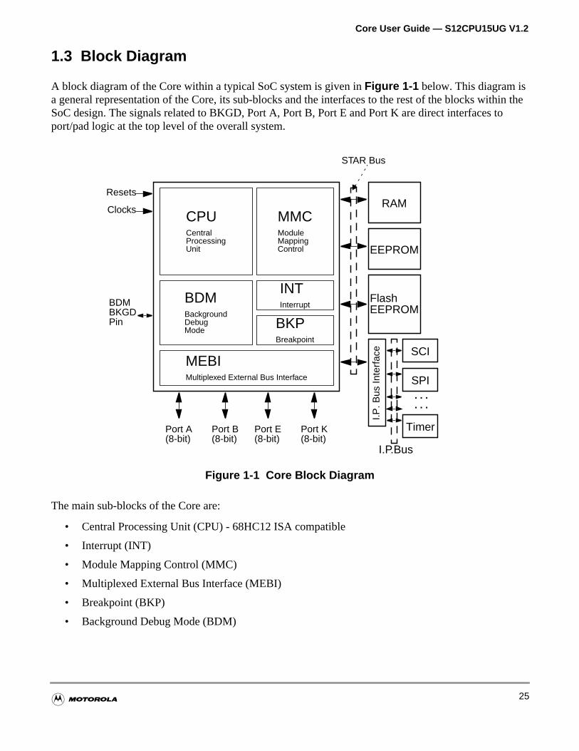
A block diagram of the Core within a typical SoC system is given inFigure 1-1 below. This diagram isa general representation of the Core, its sub-blocks and the interfaces to the rest of the blocks witSoC design. The signals related to BKGD, Port A, Port B, Port E and Port K are direct interfaces tport/pad logic at the top level of the overall system.
Figure 1-1 Core Block Diagram
The main sub-blocks of the Core are:
• Central Processing Unit (CPU) - 68HC12 ISA compatible
• Interrupt (INT)
• Module Mapping Control (MMC)
• Multiplexed External Bus Interface (MEBI)
• Breakpoint (BKP)
• Background Debug Mode (BDM)
BDMBackgroundDebugMode
CPUCentralProcessingUnit
MMCModuleMappingControl
INTInterrupt
BKPBreakpoint
MEBIMultiplexed External Bus Interface
Resets
Clocks
BDMBKGDPin
Port A(8-bit)
Port B(8-bit)
Port E(8-bit)
Port K(8-bit)
RAM
EEPROM
FlashEEPROM
I.P. B
us In
terf
ace
. . .
. . .
SCI
SPI
Timer
STAR Bus
I.P.Bus
25
Core User Guide — S12CPU15UG V1.2
g with
CPU INTn), 1 thespace
Bus) as
dlingfint, to
BDM
s and
please
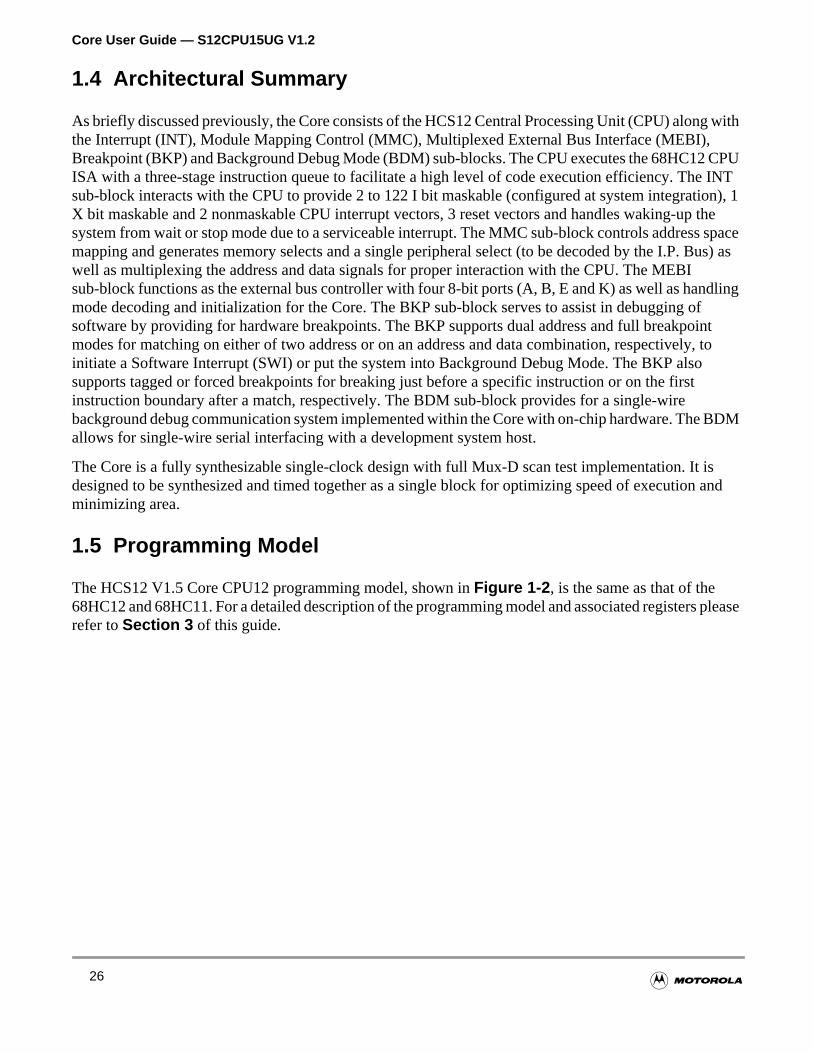
1.4 Architectural Summary
As briefly discussed previously, the Core consists of the HCS12 Central Processing Unit (CPU) alonthe Interrupt (INT), Module Mapping Control (MMC), Multiplexed External Bus Interface (MEBI),Breakpoint (BKP) and Background Debug Mode (BDM) sub-blocks. The CPU executes the 68HC12ISA with a three-stage instruction queue to facilitate a high level of code execution efficiency. Thesub-block interacts with the CPU to provide 2 to 122 I bit maskable (configured at system integratioX bit maskable and 2 nonmaskable CPU interrupt vectors, 3 reset vectors and handles waking-upsystem from wait or stop mode due to a serviceable interrupt. The MMC sub-block controls addressmapping and generates memory selects and a single peripheral select (to be decoded by the I.P.well as multiplexing the address and data signals for proper interaction with the CPU. The MEBIsub-block functions as the external bus controller with four 8-bit ports (A, B, E and K) as well as hanmode decoding and initialization for the Core. The BKP sub-block serves to assist in debugging osoftware by providing for hardware breakpoints. The BKP supports dual address and full breakpomodes for matching on either of two address or on an address and data combination, respectivelyinitiate a Software Interrupt (SWI) or put the system into Background Debug Mode. The BKP alsosupports tagged or forced breakpoints for breaking just before a specific instruction or on the firstinstruction boundary after a match, respectively. The BDM sub-block provides for a single-wirebackground debug communication system implemented within the Core with on-chip hardware. Theallows for single-wire serial interfacing with a development system host.
The Core is a fully synthesizable single-clock design with full Mux-D scan test implementation. It idesigned to be synthesized and timed together as a single block for optimizing speed of executionminimizing area.
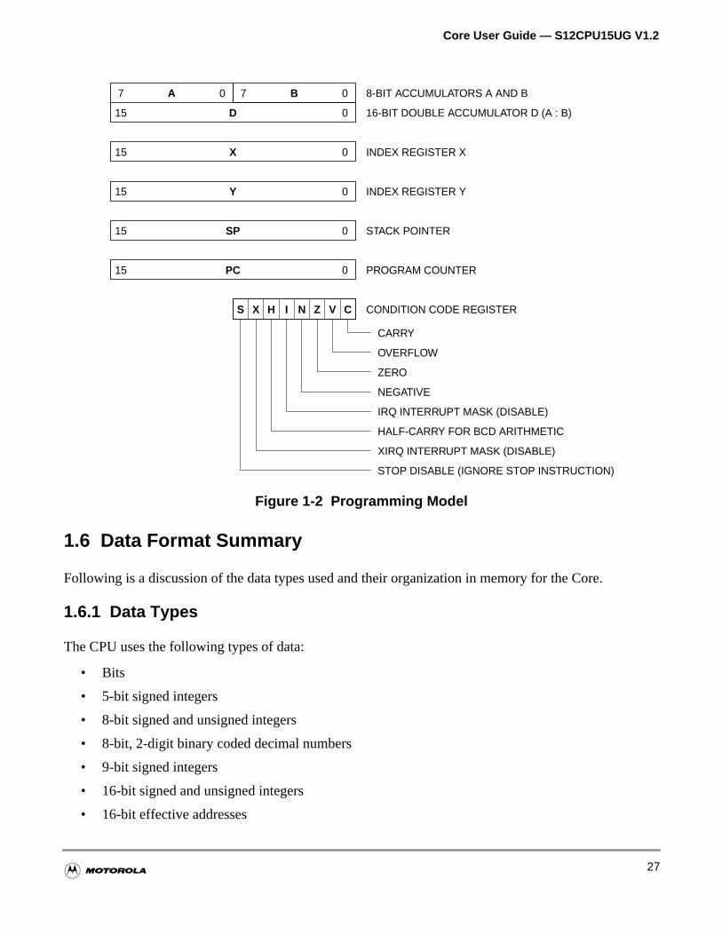
1.5 Programming Model
The HCS12 V1.5 Core CPU12 programming model, shown inFigure 1-2 , is the same as that of the68HC12 and 68HC11. For a detailed description of the programming model and associated registersrefer toSection 3 of this guide.
26
Core User Guide — S12CPU15UG V1.2
Figure 1-2 Programming Model
1.6 Data Format Summary
Following is a discussion of the data types used and their organization in memory for the Core.
1.6.1 Data Types
The CPU uses the following types of data:
• Bits
• 5-bit signed integers
• 8-bit signed and unsigned integers
• 8-bit, 2-digit binary coded decimal numbers
• 9-bit signed integers
• 16-bit signed and unsigned integers
• 16-bit effective addresses
7
15
15
15
15
15
D
X
Y
SP
PC
A B
NS X H I Z V C
0
0
0
0
0
0
70
CONDITION CODE REGISTER
8-BIT ACCUMULATORS A AND B
16-BIT DOUBLE ACCUMULATOR D (A : B)
INDEX REGISTER X
INDEX REGISTER Y
STACK POINTER
PROGRAM COUNTER
STOP DISABLE (IGNORE STOP INSTRUCTION)
CARRY
OVERFLOW
ZERO
NEGATIVE
IRQ INTERRUPT MASK (DISABLE)
HALF-CARRY FOR BCD ARITHMETIC
XIRQ INTERRUPT MASK (DISABLE)
27
Core User Guide — S12CPU15UG V1.2
-bitds are
s todows
aluese to be high
ccessnfigured
• 32-bit signed and unsigned integers
NOTE: Negative integers are represented in two’s complement form.
Five-bit and 9-bit signed integers are used only as offsets for indexed addressing modes. Sixteeneffective addresses are formed during addressing mode computations. Thirty-two-bit integer dividenused by extended division instructions. Extended multiply and extended multiply-and-accumulateinstructions produce 32-bit products.
1.6.2 Memory Organization
The standard HCS12 Core address space is 64K bytes. However, the CPU has special instructionsupport paged memory expansion which increases the standard area by means of predefined winwithin the available address space. SeeSection 11 Module Mapping Control (MMC) for moreinformation.
Eight-bit values can be stored at any odd or even byte address in available memory. Sixteen-bit voccupy two consecutive memory locations; the high byte is in the lowest address, but does not havaligned to an even boundary. Thirty-two-bit values occupy four consecutive memory locations; thebyte is in the lowest address, but does not have to be aligned to an even boundary.
All I/O and all on-chip peripherals are memory-mapped. No special instruction syntax is required to athese addresses. On-chip register and memory mapping are determined at the SoC level and are coduring integration of the Core into the system.
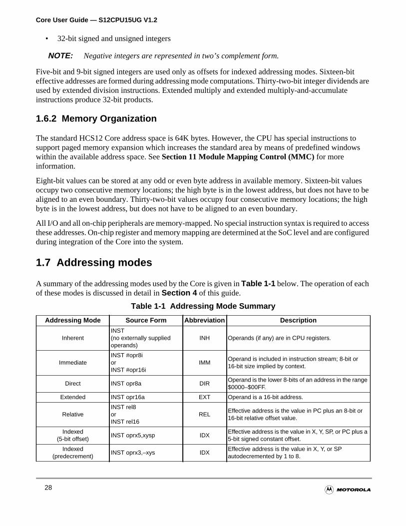
1.7 Addressing modes
A summary of the addressing modes used by the Core is given inTable 1-1 below. The operation of eachof these modes is discussed in detail inSection 4 of this guide.
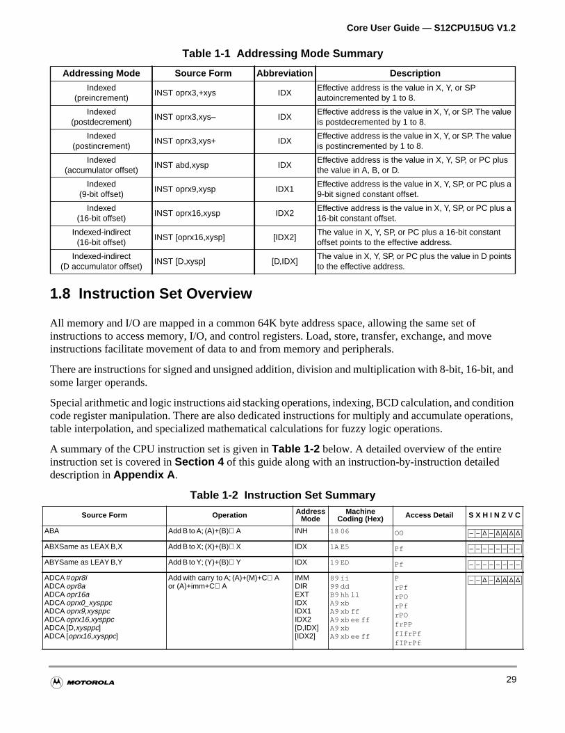
Table 1-1 Addressing Mode Summary
Addressing Mode Source Form Abbreviation Description
InherentINST(no externally suppliedoperands)
INH Operands (if any) are in CPU registers.
ImmediateINST #opr8iorINST #opr16i
IMMOperand is included in instruction stream; 8-bit or16-bit size implied by context.
Direct INST opr8a DIROperand is the lower 8-bits of an address in the range$0000–$00FF.
Extended INST opr16a EXT Operand is a 16-bit address.
RelativeINST rel8orINST rel16
RELEffective address is the value in PC plus an 8-bit or16-bit relative offset value.
Indexed(5-bit offset)
INST oprx5,xysp IDXEffective address is the value in X, Y, SP, or PC plus a5-bit signed constant offset.
Indexed(predecrement)
INST oprx3,–xys IDXEffective address is the value in X, Y, or SPautodecremented by 1 to 8.
28
Core User Guide — S12CPU15UG V1.2
ve
and
ditionations,
1.8 Instruction Set Overview
All memory and I/O are mapped in a common 64K byte address space, allowing the same set ofinstructions to access memory, I/O, and control registers. Load, store, transfer, exchange, and moinstructions facilitate movement of data to and from memory and peripherals.
There are instructions for signed and unsigned addition, division and multiplication with 8-bit, 16-bit,some larger operands.
Special arithmetic and logic instructions aid stacking operations, indexing, BCD calculation, and concode register manipulation. There are also dedicated instructions for multiply and accumulate opertable interpolation, and specialized mathematical calculations for fuzzy logic operations.
A summary of the CPU instruction set is given inTable 1-2 below. A detailed overview of the entireinstruction set is covered inSection 4 of this guide along with an instruction-by-instruction detaileddescription inAppendix A .
Table 1-2 Instruction Set Summary
Indexed(preincrement)
INST oprx3,+xys IDXEffective address is the value in X, Y, or SPautoincremented by 1 to 8.
Indexed(postdecrement)
INST oprx3,xys– IDXEffective address is the value in X, Y, or SP. The valueis postdecremented by 1 to 8.
Indexed(postincrement)
INST oprx3,xys+ IDXEffective address is the value in X, Y, or SP. The valueis postincremented by 1 to 8.
Indexed(accumulator offset)
INST abd,xysp IDXEffective address is the value in X, Y, SP, or PC plusthe value in A, B, or D.
Indexed(9-bit offset)
INST oprx9,xysp IDX1Effective address is the value in X, Y, SP, or PC plus a9-bit signed constant offset.
Indexed(16-bit offset)
INST oprx16,xysp IDX2Effective address is the value in X, Y, SP, or PC plus a16-bit constant offset.
Indexed-indirect(16-bit offset)
INST [oprx16,xysp] [IDX2]The value in X, Y, SP, or PC plus a 16-bit constantoffset points to the effective address.
Indexed-indirect(D accumulator offset)
INST [D,xysp] [D,IDX]The value in X, Y, SP, or PC plus the value in D pointsto the effective address.
Source Form Operation AddressMode
MachineCoding (Hex) Access Detail S X H I N Z V C
ABA Add B to A; (A)+(B)⇒A INH 18 06 OO
ABXSame as LEAX B,X Add B to X; (X)+(B)⇒X IDX 1A E5 Pf
ABYSame as LEAY B,Y Add B to Y; (Y)+(B)⇒Y IDX 19 ED Pf
ADCA #opr8iADCA opr8aADCA opr16aADCA oprx0_xysppcADCA oprx9,xysppcADCA oprx16,xysppcADCA [D,xysppc]ADCA [oprx16,xysppc]
Add with carry to A; (A)+(M)+C⇒Aor (A)+imm+C⇒A
IMMDIREXTIDXIDX1IDX2[D,IDX][IDX2]
89 ii99 ddB9 hh llA9 xbA9 xb ffA9 xb ee ffA9 xbA9 xb ee ff
PrPfrPOrPfrPOfrPPfIfrPffIPrPf
Table 1-1 Addressing Mode Summary
Addressing Mode Source Form Abbreviation Description
– – ∆ – ∆ ∆ ∆ ∆
– – – – – – – –
– – – – – – – –
– – ∆ – ∆ ∆ ∆ ∆
29
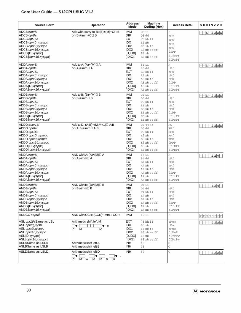
Core User Guide — S12CPU15UG V1.2
ADCB #opr8iADCB opr8aADCB opr16aADCB oprx0_xysppcADCB oprx9,xysppcADCB oprx16,xysppcADCB [D,xysppc]ADCB [oprx16,xysppc]
Add with carry to B; (B)+(M)+C⇒Bor (B)+imm+C⇒B
IMMDIREXTIDXIDX1IDX2[D,IDX][IDX2]
C9 iiD9 ddF9 hh llE9 xbE9 xb ffE9 xb ee ffE9 xbE9 xb ee ff
PrPfrPOrPfrPOfrPPfIfrPffIPrPf
ADDA #opr8iADDA opr8aADDA opr16aADDA oprx0_xysppcADDA oprx9,xysppcADDA oprx16,xysppcADDA [D,xysppc]ADDA [oprx16,xysppc]
Add to A; (A)+(M)⇒Aor (A)+imm⇒A
IMMDIREXTIDXIDX1IDX2[D,IDX][IDX2]
8B ii9B ddBB hh llAB xbAB xb ffAB xb ee ffAB xbAB xb ee ff
PrPfrPOrPfrPOfrPPfIfrPffIPrPf
ADDB #opr8iADDB opr8aADDB opr16aADDB oprx0_xysppcADDB oprx9,xysppcADDB oprx16,xysppcADDB [D,xysppc]ADDB [oprx16,xysppc]
Add to B; (B)+(M)⇒Bor (B)+imm⇒B
IMMDIREXTIDXIDX1IDX2[D,IDX][IDX2]
CB iiDB ddFB hh llEB xbEB xb ffEB xb ee ffEB xbEB xb ee ff
PrPfrPOrPfrPOfrPPfIfrPffIPrPf
ADDD #opr16iADDD opr8aADDD opr16aADDD oprx0_xysppcADDD oprx9,xysppcADDD oprx16,xysppcADDD [D,xysppc]ADDD [oprx16,xysppc]
Add to D; (A:B)+(M:M+1)⇒A:Bor (A:B)+imm⇒A:B
IMMDIREXTIDXIDX1IDX2[D,IDX][IDX2]
C3 jj kkD3 ddF3 hh llE3 xbE3 xb ffE3 xb ee ffE3 xbE3 xb ee ff
PORPfRPORPfRPOfRPPfIfRPffIPRPf
ANDA #opr8iANDA opr8aANDA opr16aANDA oprx0_xysppcANDA oprx9,xysppcANDA oprx16,xysppcANDA [D,xysppc]ANDA [oprx16,xysppc]
AND with A; (A)•(M)⇒Aor (A)•imm⇒A
IMMDIREXTIDXIDX1IDX2[D,IDX][IDX2]
84 ii94 ddB4 hh llA4 xbA4 xb ffA4 xb ee ffA4 xbA4 xb ee ff
PrPfrPOrPfrPOfrPPfIfrPffIPrPf
ANDB #opr8iANDB opr8aANDB opr16aANDB oprx0_xysppcANDB oprx9,xysppcANDB oprx16,xysppcANDB [D,xysppc]ANDB [oprx16,xysppc]
AND with B; (B)•(M)⇒Bor (B)•imm⇒B
IMMDIREXTIDXIDX1IDX2[D,IDX][IDX2]
C4 iiD4 ddF4 hh llE4 xbE4 xb ffE4 xb ee ffE4 xbE4 xb ee ff
PrPfrPOrPfrPOfrPPfIfrPffIPrPf
ANDCC #opr8i AND with CCR; (CCR)•imm⇒CCR IMM 10 ii P
ASL opr16aSame as LSLASL oprx0_xyspASL oprx9,xysppcASL oprx16,xysppcASL [D,xysppc]ASL [oprx16,xysppc]ASLASame as LSLAASLBSame as LSLB
Arithmetic shift left M
Arithmetic shift left AArithmetic shift left B
EXTIDXIDX1IDX2[D,IDX][IDX2]INHINH
78 hh ll68 xb68 xb ff68 xb ee ff68 xb68 xb ee ff4858
rPwOrPwrPwOfrPwPfIfrPwfIPrPwOO
ASLDSame as LSLD Arithmetic shift left D INH 59 O
Source Form Operation AddressMode
MachineCoding (Hex) Access Detail S X H I N Z V C
– – ∆ – ∆ ∆ ∆ ∆
– – ∆ – ∆ ∆ ∆ ∆
– – ∆ – ∆ ∆ ∆ ∆
– – – – ∆ ∆ ∆ ∆
– – – – ∆ ∆ 0 –
– – – – ∆ ∆ 0 –
⇓ ⇓ ⇓ ⇓ ⇓ ⇓ ⇓ ⇓
C0
b7 b0
– – – – ∆ ∆ ∆ ∆
• • • • • •
C0
b7 b0A Bb7b0
– – – – ∆ ∆ ∆ ∆
30
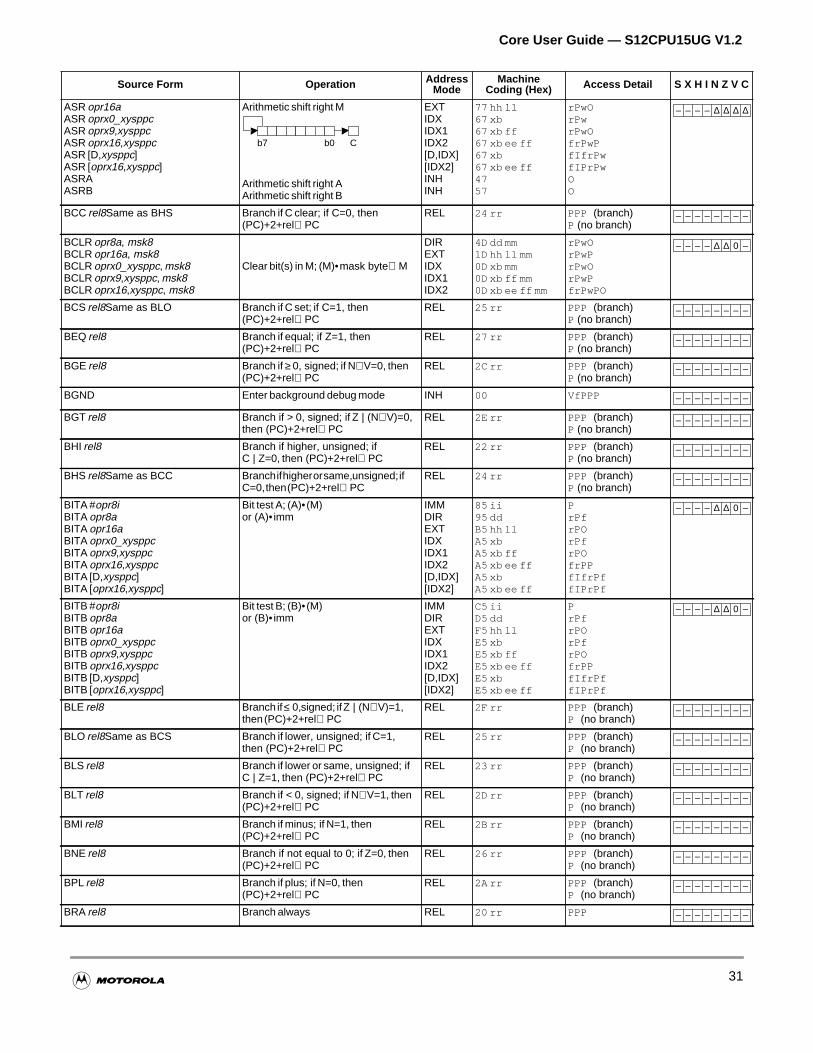
Core User Guide — S12CPU15UG V1.2
ASR opr16aASR oprx0_xysppcASR oprx9,xysppcASR oprx16,xysppcASR [D,xysppc]ASR [oprx16,xysppc]ASRAASRB
Arithmetic shift right M
Arithmetic shift right AArithmetic shift right B
EXTIDXIDX1IDX2[D,IDX][IDX2]INHINH
77 hh ll67 xb67 xb ff67 xb ee ff67 xb67 xb ee ff4757
rPwOrPwrPwOfrPwPfIfrPwfIPrPwOO
BCC rel8Same as BHS Branch if C clear; if C=0, then(PC)+2+rel⇒PC
REL 24 rr PPP (branch)P (no branch)
BCLR opr8a, msk8BCLR opr16a, msk8BCLR oprx0_xysppc, msk8BCLR oprx9,xysppc, msk8BCLR oprx16,xysppc, msk8
Clear bit(s) in M; (M)•mask byte⇒M
DIREXTIDXIDX1IDX2
4D dd mm1D hh ll mm0D xb mm0D xb ff mm0D xb ee ff mm
rPwOrPwPrPwOrPwPfrPwPO
BCS rel8Same as BLO Branch if C set; if C=1, then(PC)+2+rel⇒PC
REL 25 rr PPP (branch)P (no branch)
BEQ rel8 Branch if equal; if Z=1, then(PC)+2+rel⇒PC
REL 27 rr PPP (branch)P (no branch)
BGE rel8 Branch if ≥ 0, signed; if N⊕V=0, then(PC)+2+rel⇒PC
REL 2C rr PPP (branch)P (no branch)
BGND Enter background debug mode INH 00 VfPPP
BGT rel8 Branch if > 0, signed; if Z | (N⊕V)=0,then (PC)+2+rel⇒PC
REL 2E rr PPP (branch)P (no branch)
BHI rel8 Branch if higher, unsigned; ifC | Z=0, then (PC)+2+rel⇒PC
REL 22 rr PPP (branch)P (no branch)
BHS rel8Same as BCC Branchifhigherorsame,unsigned;ifC=0,then(PC)+2+rel⇒PC
REL 24 rr PPP (branch)P (no branch)
BITA #opr8iBITA opr8aBITA opr16aBITA oprx0_xysppcBITA oprx9,xysppcBITA oprx16,xysppcBITA [D,xysppc]BITA [oprx16,xysppc]
Bit test A; (A)•(M)or (A)•imm
IMMDIREXTIDXIDX1IDX2[D,IDX][IDX2]
85 ii95 ddB5 hh llA5 xbA5 xb ffA5 xb ee ffA5 xbA5 xb ee ff
PrPfrPOrPfrPOfrPPfIfrPffIPrPf
BITB #opr8iBITB opr8aBITB opr16aBITB oprx0_xysppcBITB oprx9,xysppcBITB oprx16,xysppcBITB [D,xysppc]BITB [oprx16,xysppc]
Bit test B; (B)•(M)or (B)•imm
IMMDIREXTIDXIDX1IDX2[D,IDX][IDX2]
C5 iiD5 ddF5 hh llE5 xbE5 xb ffE5 xb ee ffE5 xbE5 xb ee ff
PrPfrPOrPfrPOfrPPfIfrPffIPrPf
BLE rel8 Branch if≤ 0,signed; ifZ | (N⊕V)=1,then(PC)+2+rel⇒PC
REL 2F rr PPP (branch)P (no branch)
BLO rel8Same as BCS Branch if lower, unsigned; if C=1,then (PC)+2+rel⇒PC
REL 25 rr PPP (branch)P (no branch)
BLS rel8 Branch if lower or same, unsigned; ifC | Z=1, then (PC)+2+rel⇒PC
REL 23 rr PPP (branch)P (no branch)
BLT rel8 Branch if < 0, signed; if N⊕V=1, then(PC)+2+rel⇒PC
REL 2D rr PPP (branch)P (no branch)
BMI rel8 Branch if minus; if N=1, then(PC)+2+rel⇒PC
REL 2B rr PPP (branch)P (no branch)
BNE rel8 Branch if not equal to 0; if Z=0, then(PC)+2+rel⇒PC
REL 26 rr PPP (branch)P (no branch)
BPL rel8 Branch if plus; if N=0, then(PC)+2+rel⇒PC
REL 2A rr PPP (branch)P (no branch)
BRA rel8 Branch always REL 20 rr PPP
Source Form Operation AddressMode
MachineCoding (Hex) Access Detail S X H I N Z V C
Cb7 b0
– – – – ∆ ∆ ∆ ∆
– – – – – – – –
– – – – ∆ ∆ 0 –
– – – – – – – –
– – – – – – – –
– – – – – – – –
– – – – – – – –
– – – – – – – –
– – – – – – – –
– – – – – – – –
– – – – ∆ ∆ 0 –
– – – – ∆ ∆ 0 –
– – – – – – – –
– – – – – – – –
– – – – – – – –
– – – – – – – –
– – – – – – – –
– – – – – – – –
– – – – – – – –
– – – – – – – –
31
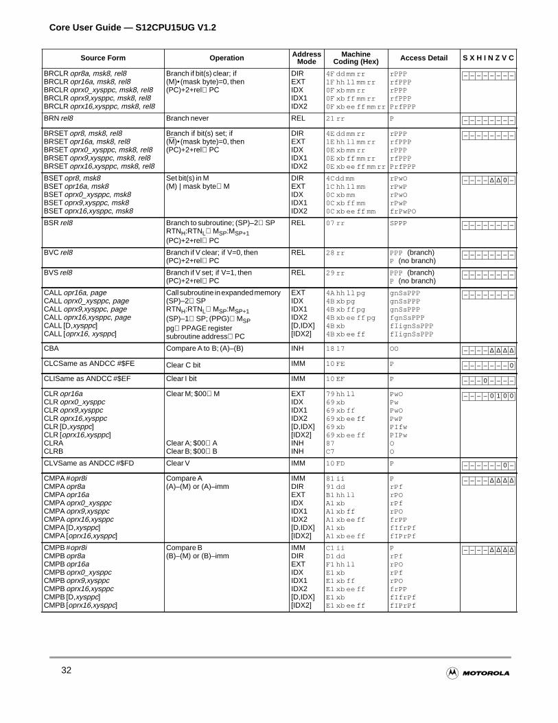
Core User Guide — S12CPU15UG V1.2
BRCLR opr8a, msk8, rel8BRCLR opr16a, msk8, rel8BRCLR oprx0_xysppc, msk8, rel8BRCLR oprx9,xysppc, msk8, rel8BRCLR oprx16,xysppc, msk8, rel8
Branch if bit(s) clear; if(M)•(mask byte)=0, then(PC)+2+rel⇒PC
DIREXTIDXIDX1IDX2
4F dd mm rr1F hh ll mm rr0F xb mm rr0F xb ff mm rr0F xb ee ff mm rr
rPPPrfPPPrPPPrfPPPPrfPPP
BRN rel8 Branch never REL 21 rr P
BRSET opr8, msk8, rel8BRSET opr16a, msk8, rel8BRSET oprx0_xysppc, msk8, rel8BRSET oprx9,xysppc, msk8, rel8BRSET oprx16,xysppc, msk8, rel8
Branch if bit(s) set; if(M)•(mask byte)=0, then(PC)+2+rel⇒PC
DIREXTIDXIDX1IDX2
4E dd mm rr1E hh ll mm rr0E xb mm rr0E xb ff mm rr0E xb ee ff mm rr
rPPPrfPPPrPPPrfPPPPrfPPP
BSET opr8, msk8BSET opr16a, msk8BSET oprx0_xysppc, msk8BSET oprx9,xysppc, msk8BSET oprx16,xysppc, msk8
Set bit(s) in M(M) | mask byte⇒M
DIREXTIDXIDX1IDX2
4Cdd mm1C hh ll mm0C xb mm0C xb ff mm0C xb ee ff mm
rPwOrPwPrPwOrPwPfrPwPO
BSR rel8 Branch to subroutine; (SP)–2⇒SPRTNH:RTNL⇒MSP:MSP+1(PC)+2+rel⇒PC
REL 07 rr SPPP
BVC rel8 Branch if V clear; if V=0, then(PC)+2+rel⇒PC
REL 28 rr PPP (branch)P (no branch)
BVS rel8 Branch if V set; if V=1, then(PC)+2+rel⇒PC
REL 29 rr PPP (branch)P (no branch)
CALL opr16a, pageCALL oprx0_xysppc, pageCALL oprx9,xysppc, pageCALL oprx16,xysppc, pageCALL [D,xysppc]CALL [oprx16, xysppc]
Call subroutine inexpandedmemory(SP)–2⇒SPRTNH:RTNL⇒MSP:MSP+1(SP)–1⇒SP; (PPG)⇒MSPpg⇒PPAGE registersubroutine address⇒PC
EXTIDXIDX1IDX2[D,IDX][IDX2]
4A hh ll pg4B xb pg4B xb ff pg4B xb ee ff pg4B xb4B xb ee ff
gnSsPPPgnSsPPPgnSsPPPfgnSsPPPfIignSsPPPfIignSsPPP
CBA Compare A to B; (A)–(B) INH 18 17 OO
CLCSame as ANDCC #$FE Clear C bit IMM 10 FE P
CLISame as ANDCC #$EF Clear I bit IMM 10 EF P
CLR opr16aCLR oprx0_xysppcCLR oprx9,xysppcCLR oprx16,xysppcCLR [D,xysppc]CLR [oprx16,xysppc]CLRACLRB
Clear M; $00⇒M
Clear A; $00⇒AClear B; $00⇒B
EXTIDXIDX1IDX2[D,IDX][IDX2]INHINH
79 hh ll69 xb69 xb ff69 xb ee ff69 xb69 xb ee ff87C7
PwOPwPwOPwPPIfwPIPwOO
CLVSame as ANDCC #$FD Clear V IMM 10 FD P
CMPA #opr8iCMPA opr8aCMPA opr16aCMPA oprx0_xysppcCMPA oprx9,xysppcCMPA oprx16,xysppcCMPA [D,xysppc]CMPA [oprx16,xysppc]
Compare A(A)–(M) or (A)–imm
IMMDIREXTIDXIDX1IDX2[D,IDX][IDX2]
81 ii91 ddB1 hh llA1 xbA1 xb ffA1 xb ee ffA1 xbA1 xb ee ff
PrPfrPOrPfrPOfrPPfIfrPffIPrPf
CMPB #opr8iCMPB opr8aCMPB opr16aCMPB oprx0_xysppcCMPB oprx9,xysppcCMPB oprx16,xysppcCMPB [D,xysppc]CMPB [oprx16,xysppc]
Compare B(B)–(M) or (B)–imm
IMMDIREXTIDXIDX1IDX2[D,IDX][IDX2]
C1 iiD1 ddF1 hh llE1 xbE1 xb ffE1 xb ee ffE1 xbE1 xb ee ff
PrPfrPOrPfrPOfrPPfIfrPffIPrPf
Source Form Operation AddressMode
MachineCoding (Hex) Access Detail S X H I N Z V C
– – – – – – – –
– – – – – – – –
– – – – – – – –
– – – – ∆ ∆ 0 –
– – – – – – – –
– – – – – – – –
– – – – – – – –
– – – – – – – –
– – – – ∆ ∆ ∆ ∆
– – – – – – – 0
– – – 0 – – – –
– – – – 0 1 0 0
– – – – – – 0 –
– – – – ∆ ∆ ∆ ∆
– – – – ∆ ∆ ∆ ∆
32
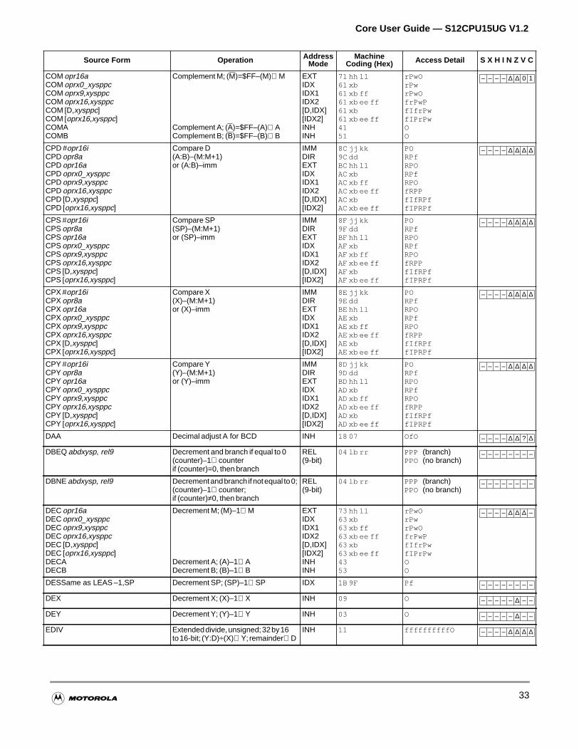
Core User Guide — S12CPU15UG V1.2
COM opr16aCOM oprx0_xysppcCOM oprx9,xysppcCOM oprx16,xysppcCOM [D,xysppc]COM [oprx16,xysppc]COMACOMB
Complement M; (M)=$FF–(M)⇒M
Complement A; (A)=$FF–(A)⇒AComplement B; (B)=$FF–(B)⇒B
EXTIDXIDX1IDX2[D,IDX][IDX2]INHINH
71 hh ll61 xb61 xb ff61 xb ee ff61 xb61 xb ee ff4151
rPwOrPwrPwOfrPwPfIfrPwfIPrPwOO
CPD #opr16iCPD opr8aCPD opr16aCPD oprx0_xysppcCPD oprx9,xysppcCPD oprx16,xysppcCPD [D,xysppc]CPD [oprx16,xysppc]
Compare D(A:B)–(M:M+1)or (A:B)–imm
IMMDIREXTIDXIDX1IDX2[D,IDX][IDX2]
8C jj kk9C ddBC hh llAC xbAC xb ffAC xb ee ffAC xbAC xb ee ff
PORPfRPORPfRPOfRPPfIfRPffIPRPf
CPS #opr16iCPS opr8aCPS opr16aCPS oprx0_xysppcCPS oprx9,xysppcCPS oprx16,xysppcCPS [D,xysppc]CPS [oprx16,xysppc]
Compare SP(SP)–(M:M+1)or (SP)–imm
IMMDIREXTIDXIDX1IDX2[D,IDX][IDX2]
8F jj kk9F ddBF hh llAF xbAF xb ffAF xb ee ffAF xbAF xb ee ff
PORPfRPORPfRPOfRPPfIfRPffIPRPf
CPX #opr16iCPX opr8aCPX opr16aCPX oprx0_xysppcCPX oprx9,xysppcCPX oprx16,xysppcCPX [D,xysppc]CPX [oprx16,xysppc]
Compare X(X)–(M:M+1)or (X)–imm
IMMDIREXTIDXIDX1IDX2[D,IDX][IDX2]
8E jj kk9E ddBE hh llAE xbAE xb ffAE xb ee ffAE xbAE xb ee ff
PORPfRPORPfRPOfRPPfIfRPffIPRPf
CPY #opr16iCPY opr8aCPY opr16aCPY oprx0_xysppcCPY oprx9,xysppcCPY oprx16,xysppcCPY [D,xysppc]CPY [oprx16,xysppc]
Compare Y(Y)–(M:M+1)or (Y)–imm
IMMDIREXTIDXIDX1IDX2[D,IDX][IDX2]
8D jj kk9D ddBD hh llAD xbAD xb ffAD xb ee ffAD xbAD xb ee ff
PORPfRPORPfRPOfRPPfIfRPffIPRPf
DAA Decimal adjust A for BCD INH 18 07 OfO
DBEQ abdxysp, rel9 Decrement and branch if equal to 0(counter)–1⇒counterif (counter)=0, then branch
REL(9-bit)
04 lb rr PPP (branch)PPO (no branch)
DBNE abdxysp, rel9 Decrementandbranch ifnotequal to0;(counter)–1⇒counter;if (counter)≠0, then branch
REL(9-bit)
04 lb rr PPP (branch)PPO (no branch)
DEC opr16aDEC oprx0_xysppcDEC oprx9,xysppcDEC oprx16,xysppcDEC [D,xysppc]DEC [oprx16,xysppc]DECADECB
Decrement M; (M)–1⇒M
Decrement A; (A)–1⇒ADecrement B; (B)–1⇒B
EXTIDXIDX1IDX2[D,IDX][IDX2]INHINH
73 hh ll63 xb63 xb ff63 xb ee ff63 xb63 xb ee ff4353
rPwOrPwrPwOfrPwPfIfrPwfIPrPwOO
DESSame as LEAS –1,SP Decrement SP; (SP)–1⇒SP IDX 1B 9F Pf
DEX Decrement X; (X)–1⇒X INH 09 O
DEY Decrement Y; (Y)–1⇒Y INH 03 O
EDIV Extendeddivide,unsigned;32by16to16-bit; (Y:D)÷(X)⇒Y; remainder⇒D
INH 11 ffffffffffO
Source Form Operation AddressMode
MachineCoding (Hex) Access Detail S X H I N Z V C
– – – – ∆ ∆ 0 1
– – – – ∆ ∆ ∆ ∆
– – – – ∆ ∆ ∆ ∆
– – – – ∆ ∆ ∆ ∆
– – – – ∆ ∆ ∆ ∆
– – – – ∆ ∆ ? ∆
– – – – – – – –
– – – – – – – –
– – – – ∆ ∆ ∆ –
– – – – – – – –
– – – – – ∆ – –
– – – – – ∆ – –
– – – – ∆ ∆ ∆ ∆
33
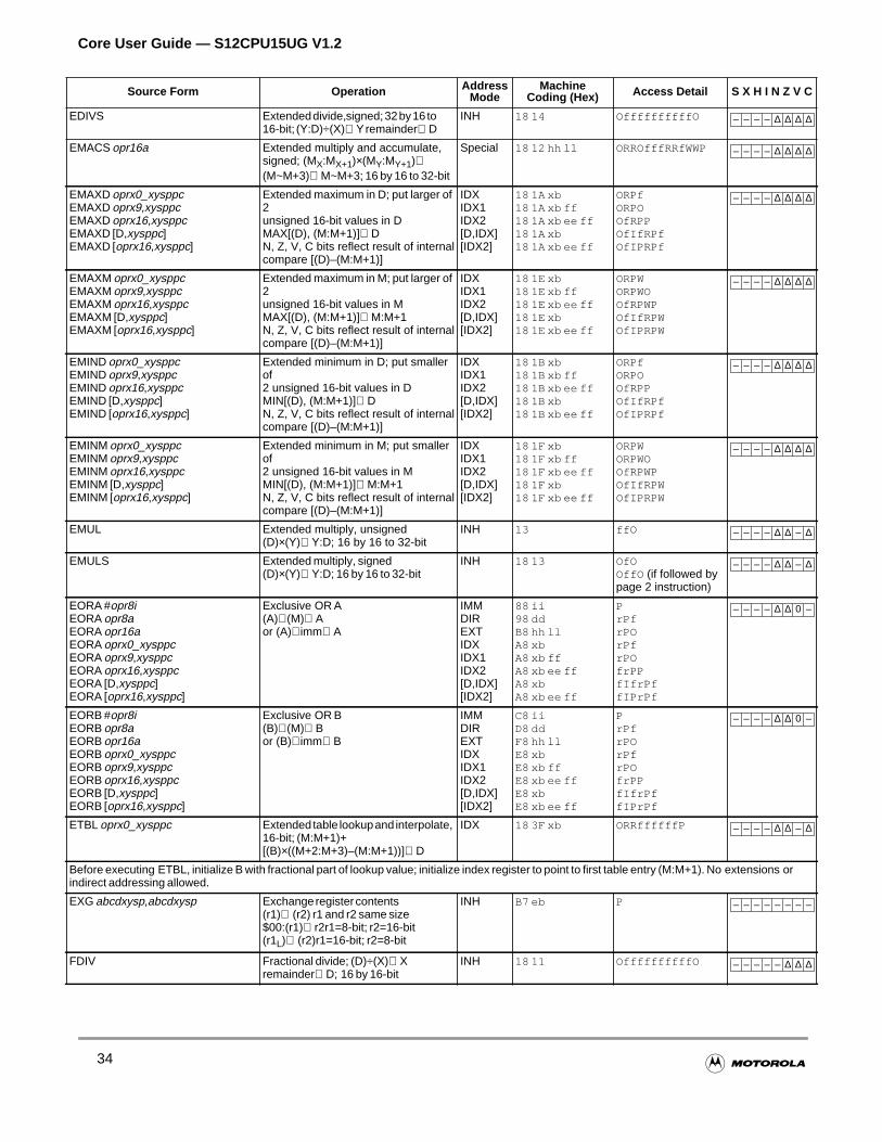
Core User Guide — S12CPU15UG V1.2
EDIVS Extendeddivide,signed;32by16 to16-bit; (Y:D)÷(X)⇒Yremainder⇒D
INH 18 14 OffffffffffO
EMACS opr16a Extended multiply and accumulate,signed; (MX:MX+1)×(MY:MY+1)+(M~M+3)⇒M~M+3; 16 by 16 to 32-bit
Special 18 12 hh ll ORROfffRRfWWP
EMAXD oprx0_xysppcEMAXD oprx9,xysppcEMAXD oprx16,xysppcEMAXD [D,xysppc]EMAXD [oprx16,xysppc]
Extended maximum in D; put larger of2unsigned 16-bit values in DMAX[(D), (M:M+1)]⇒DN, Z, V, C bits reflect result of internalcompare [(D)–(M:M+1)]
IDXIDX1IDX2[D,IDX][IDX2]
18 1A xb18 1A xb ff18 1A xb ee ff18 1A xb18 1A xb ee ff
ORPfORPOOfRPPOfIfRPfOfIPRPf
EMAXM oprx0_xysppcEMAXM oprx9,xysppcEMAXM oprx16,xysppcEMAXM [D,xysppc]EMAXM [oprx16,xysppc]
Extended maximum in M; put larger of2unsigned 16-bit values in MMAX[(D), (M:M+1)]⇒M:M+1N, Z, V, C bits reflect result of internalcompare [(D)–(M:M+1)]
IDXIDX1IDX2[D,IDX][IDX2]
18 1E xb18 1E xb ff18 1E xb ee ff18 1E xb18 1E xb ee ff
ORPWORPWOOfRPWPOfIfRPWOfIPRPW
EMIND oprx0_xysppcEMIND oprx9,xysppcEMIND oprx16,xysppcEMIND [D,xysppc]EMIND [oprx16,xysppc]
Extended minimum in D; put smallerof2 unsigned 16-bit values in DMIN[(D), (M:M+1)]⇒DN, Z, V, C bits reflect result of internalcompare [(D)–(M:M+1)]
IDXIDX1IDX2[D,IDX][IDX2]
18 1B xb18 1B xb ff18 1B xb ee ff18 1B xb18 1B xb ee ff
ORPfORPOOfRPPOfIfRPfOfIPRPf
EMINM oprx0_xysppcEMINM oprx9,xysppcEMINM oprx16,xysppcEMINM [D,xysppc]EMINM [oprx16,xysppc]
Extended minimum in M; put smallerof2 unsigned 16-bit values in MMIN[(D), (M:M+1)]⇒M:M+1N, Z, V, C bits reflect result of internalcompare [(D)–(M:M+1)]
IDXIDX1IDX2[D,IDX][IDX2]
18 1F xb18 1F xb ff18 1F xb ee ff18 1F xb18 1F xb ee ff
ORPWORPWOOfRPWPOfIfRPWOfIPRPW
EMUL Extended multiply, unsigned(D)×(Y)⇒Y:D; 16 by 16 to 32-bit
INH 13 ffO
EMULS Extended multiply, signed(D)×(Y)⇒Y:D; 16 by 16 to 32-bit
INH 18 13 OfOOffO (if followed bypage 2 instruction)
EORA #opr8iEORA opr8aEORA opr16aEORA oprx0_xysppcEORA oprx9,xysppcEORA oprx16,xysppcEORA [D,xysppc]EORA [oprx16,xysppc]
Exclusive OR A(A)⊕(M)⇒Aor (A)⊕imm⇒A
IMMDIREXTIDXIDX1IDX2[D,IDX][IDX2]
88 ii98 ddB8 hh llA8 xbA8 xb ffA8 xb ee ffA8 xbA8 xb ee ff
PrPfrPOrPfrPOfrPPfIfrPffIPrPf
EORB #opr8iEORB opr8aEORB opr16aEORB oprx0_xysppcEORB oprx9,xysppcEORB oprx16,xysppcEORB [D,xysppc]EORB [oprx16,xysppc]
Exclusive OR B(B)⊕(M)⇒Bor (B)⊕imm⇒B
IMMDIREXTIDXIDX1IDX2[D,IDX][IDX2]
C8 iiD8 ddF8 hh llE8 xbE8 xb ffE8 xb ee ffE8 xbE8 xb ee ff
PrPfrPOrPfrPOfrPPfIfrPffIPrPf
ETBL oprx0_xysppc Extended table lookupand interpolate,16-bit; (M:M+1)+[(B)×((M+2:M+3)–(M:M+1))]⇒D
IDX 18 3F xb ORRffffffP
Before executing ETBL, initialize B with fractional part of lookup value; initialize index register to point to first table entry (M:M+1). No extensions orindirect addressing allowed.
EXG abcdxysp,abcdxysp Exchangeregistercontents(r1)⇔(r2) r1 and r2 same size$00:(r1)⇒r2r1=8-bit; r2=16-bit(r1L)⇔(r2)r1=16-bit; r2=8-bit
INH B7 eb P
FDIV Fractional divide; (D)÷(X)⇒Xremainder⇒D; 16 by 16-bit
INH 18 11 OffffffffffO
Source Form Operation AddressMode
MachineCoding (Hex) Access Detail S X H I N Z V C
– – – – ∆ ∆ ∆ ∆
– – – – ∆ ∆ ∆ ∆
– – – – ∆ ∆ ∆ ∆
– – – – ∆ ∆ ∆ ∆
– – – – ∆ ∆ ∆ ∆
– – – – ∆ ∆ ∆ ∆
– – – – ∆ ∆ – ∆
– – – – ∆ ∆ – ∆
– – – – ∆ ∆ 0 –
– – – – ∆ ∆ 0 –
– – – – ∆ ∆ – ∆
– – – – – – – –
– – – – – ∆ ∆ ∆
34
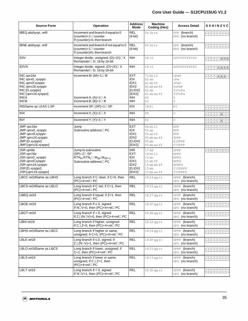
Core User Guide — S12CPU15UG V1.2
IBEQ abdxysp, rel9 Increment and branch if equal to 0(counter)+1⇒counterIf (counter)=0, then branch
REL(9-bit)
04 lb rr PPP (branch)PPO (no branch)
IBNE abdxysp, rel9 Increment and branch if not equal to 0(counter)+1⇒counterIf (counter)≠0, then branch
REL(9-bit)
04 lb rr PPP (branch)PPO (no branch)
IDIV Integer divide, unsigned; (D)÷(X)⇒XRemainder⇒D; 16 by 16-bit
INH 18 10 OffffffffffO
IDIVS Integer divide, signed; (D)÷(X)⇒XRemainder⇒D; 16 by 16-bit
INH 18 15 OffffffffffO
INC opr16aINC oprx0_xysppcINC oprx9,xysppcINC oprx16,xysppcINC [D,xysppc]INC [oprx16,xysppc]INCAINCB
Increment M; (M)+1⇒M
Increment A; (A)+1⇒AIncrement B; (B)+1⇒B
EXTIDXIDX1IDX2[D,IDX][IDX2]INHINH
72 hh ll62 xb62 xb ff62 xb ee ff62 xb62 xb ee ff4252
rPwOrPwrPwOfrPwPfIfrPwfIPrPwOO
INSSame as LEAS 1,SP Increment SP; (SP)+1⇒SP IDX 1B 81 Pf
INX Increment X; (X)+1⇒X INH 08 O
INY Increment Y; (Y)+1⇒Y INH 02 O
JMP opr16aJMP oprx0_xysppcJMP oprx9,xysppcJMP oprx16,xysppcJMP [D,xysppc]JMP [oprx16,xysppc]
JumpSubroutine address⇒PC
EXTIDXIDX1IDX2[D,IDX][IDX2]
06 hh ll05 xb05 xb ff05 xb ee ff05 xb05 xb ee ff
PPPPPPPPPfPPPfIfPPPfIfPPP
JSR opr8aJSR opr16aJSR oprx0_xysppcJSR oprx9,xysppcJSR oprx16,xysppcJSR [D,xysppc]JSR [oprx16,xysppc]
Jump to subroutine(SP)–2⇒SPRTNH:RTNL⇒MSP:MSP+1Subroutine address⇒PC
DIREXTIDXIDX1IDX2[D,IDX][IDX2]
17 dd16 hh ll15 xb15 xb ff15 xb ee ff15 xb15 xb ee ff
SPPPSPPPPPPSPPPSfPPPSfIfPPPSfIfPPPS
LBCC rel16Same as LBHS Long branch if C clear; if C=0, then(PC)+4+rel⇒PC
REL 18 24 qq rr OPPP (branch)OPO (no branch)
LBCS rel16Same as LBLO Long branch if C set; if C=1, then(PC)+4+rel⇒PC
REL 18 25 qq rr OPPP (branch)OPO (no branch)
LBEQ rel16 Long branch if equal; if Z=1, then(PC)+4+rel⇒PC
REL 18 27 qq rr OPPP (branch)OPO (no branch)
LBGE rel16 Long branch if ≥ 0, signedIf N⊕V=0, then (PC)+4+rel⇒PC
REL 18 2C qq rr OPPP (branch)OPO (no branch)
LBGT rel16 Long branch if > 0, signedIf Z | (N⊕V)=0, then (PC)+4+rel⇒PC
REL 18 2E qq rr OPPP (branch)OPO (no branch)
LBHI rel16 Long branch if higher, unsignedIf C | Z=0, then (PC)+4+rel⇒PC
REL 18 22 qq rr OPPP (branch)OPO (no branch)
LBHS rel16Same as LBCC Long branch if higher or same,unsigned; If C=0, (PC)+4+rel⇒PC
REL 18 24 qq rr OPPP (branch)OPO (no branch)
LBLE rel16 Long branch if ≤ 0, signed; ifZ | (N⊕V)=1, then (PC)+4+rel⇒PC
REL 18 2F qq rr OPPP (branch)OPO (no branch)
LBLO rel16Same as LBCS Long branch if lower, unsigned; ifC=1, then (PC)+4+rel⇒PC
REL 18 25 qq rr OPPP (branch)OPO (no branch)
LBLS rel16 Long branch if lower or same,unsigned; If C | Z=1, then(PC)+4+rel⇒PC
REL 18 23 qq rr OPPP (branch)OPO (no branch)
LBLT rel16 Long branch if < 0, signedIf N⊕V=1, then (PC)+4+rel⇒PC
REL 18 2D qq rr OPPP (branch)OPO (no branch)
Source Form Operation AddressMode
MachineCoding (Hex) Access Detail S X H I N Z V C
– – – – – – – –
– – – – – – – –
– – – – – ∆ 0 ∆
– – – – ∆ ∆ ∆ ∆
– – – – ∆ ∆ ∆ –
– – – – – – – –
– – – – – ∆ – –
– – – – – ∆ – –
– – – – – – – –
– – – – – – – –
– – – – – – – –
– – – – – – – –
– – – – – – – –
– – – – – – – –
– – – – – – – –
– – – – – – – –
– – – – – – – –
– – – – – – – –
– – – – – – – –
– – – – – – – –
– – – – – – – –
35
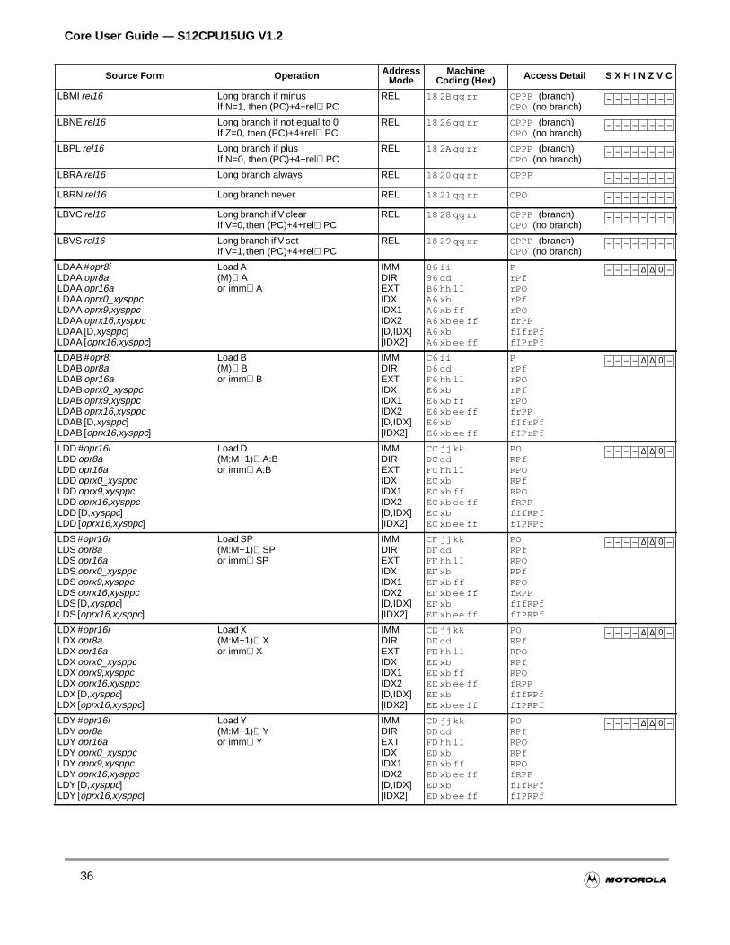
Core User Guide — S12CPU15UG V1.2
LBMI rel16 Long branch if minusIf N=1, then (PC)+4+rel⇒PC
REL 18 2B qq rr OPPP (branch)OPO (no branch)
LBNE rel16 Long branch if not equal to 0If Z=0, then (PC)+4+rel⇒PC
REL 18 26 qq rr OPPP (branch)OPO (no branch)
LBPL rel16 Long branch if plusIf N=0, then (PC)+4+rel⇒PC
REL 18 2A qq rr OPPP (branch)OPO (no branch)
LBRA rel16 Long branch always REL 18 20 qq rr OPPP
LBRN rel16 Long branch never REL 18 21 qq rr OPO
LBVC rel16 Long branch if V clearIf V=0,then (PC)+4+rel⇒PC
REL 18 28 qq rr OPPP (branch)OPO (no branch)
LBVS rel16 Long branch if V setIf V=1,then (PC)+4+rel⇒PC
REL 18 29 qq rr OPPP (branch)OPO (no branch)
LDAA #opr8iLDAA opr8aLDAA opr16aLDAA oprx0_xysppcLDAA oprx9,xysppcLDAA oprx16,xysppcLDAA [D,xysppc]LDAA [oprx16,xysppc]
Load A(M)⇒Aor imm⇒A
IMMDIREXTIDXIDX1IDX2[D,IDX][IDX2]
86 ii96 ddB6 hh llA6 xbA6 xb ffA6 xb ee ffA6 xbA6 xb ee ff
PrPfrPOrPfrPOfrPPfIfrPffIPrPf
LDAB #opr8iLDAB opr8aLDAB opr16aLDAB oprx0_xysppcLDAB oprx9,xysppcLDAB oprx16,xysppcLDAB [D,xysppc]LDAB [oprx16,xysppc]
Load B(M)⇒Bor imm⇒B
IMMDIREXTIDXIDX1IDX2[D,IDX][IDX2]
C6 iiD6 ddF6 hh llE6 xbE6 xb ffE6 xb ee ffE6 xbE6 xb ee ff
PrPfrPOrPfrPOfrPPfIfrPffIPrPf
LDD #opr16iLDD opr8aLDD opr16aLDD oprx0_xysppcLDD oprx9,xysppcLDD oprx16,xysppcLDD [D,xysppc]LDD [oprx16,xysppc]
Load D(M:M+1)⇒A:Bor imm⇒A:B
IMMDIREXTIDXIDX1IDX2[D,IDX][IDX2]
CC jj kkDC ddFC hh llEC xbEC xb ffEC xb ee ffEC xbEC xb ee ff
PORPfRPORPfRPOfRPPfIfRPffIPRPf
LDS #opr16iLDS opr8aLDS opr16aLDS oprx0_xysppcLDS oprx9,xysppcLDS oprx16,xysppcLDS [D,xysppc]LDS [oprx16,xysppc]
Load SP(M:M+1)⇒SPor imm⇒SP
IMMDIREXTIDXIDX1IDX2[D,IDX][IDX2]
CF jj kkDF ddFF hh llEF xbEF xb ffEF xb ee ffEF xbEF xb ee ff
PORPfRPORPfRPOfRPPfIfRPffIPRPf
LDX #opr16iLDX opr8aLDX opr16aLDX oprx0_xysppcLDX oprx9,xysppcLDX oprx16,xysppcLDX [D,xysppc]LDX [oprx16,xysppc]
Load X(M:M+1)⇒Xor imm⇒X
IMMDIREXTIDXIDX1IDX2[D,IDX][IDX2]
CE jj kkDE ddFE hh llEE xbEE xb ffEE xb ee ffEE xbEE xb ee ff
PORPfRPORPfRPOfRPPfIfRPffIPRPf
LDY #opr16iLDY opr8aLDY opr16aLDY oprx0_xysppcLDY oprx9,xysppcLDY oprx16,xysppcLDY [D,xysppc]LDY [oprx16,xysppc]
Load Y(M:M+1)⇒Yor imm⇒Y
IMMDIREXTIDXIDX1IDX2[D,IDX][IDX2]
CD jj kkDD ddFD hh llED xbED xb ffED xb ee ffED xbED xb ee ff
PORPfRPORPfRPOfRPPfIfRPffIPRPf
Source Form Operation AddressMode
MachineCoding (Hex) Access Detail S X H I N Z V C
– – – – – – – –
– – – – – – – –
– – – – – – – –
– – – – – – – –
– – – – – – – –
– – – – – – – –
– – – – – – – –
– – – – ∆ ∆ 0 –
– – – – ∆ ∆ 0 –
– – – – ∆ ∆ 0 –
– – – – ∆ ∆ 0 –
– – – – ∆ ∆ 0 –
– – – – ∆ ∆ 0 –
36
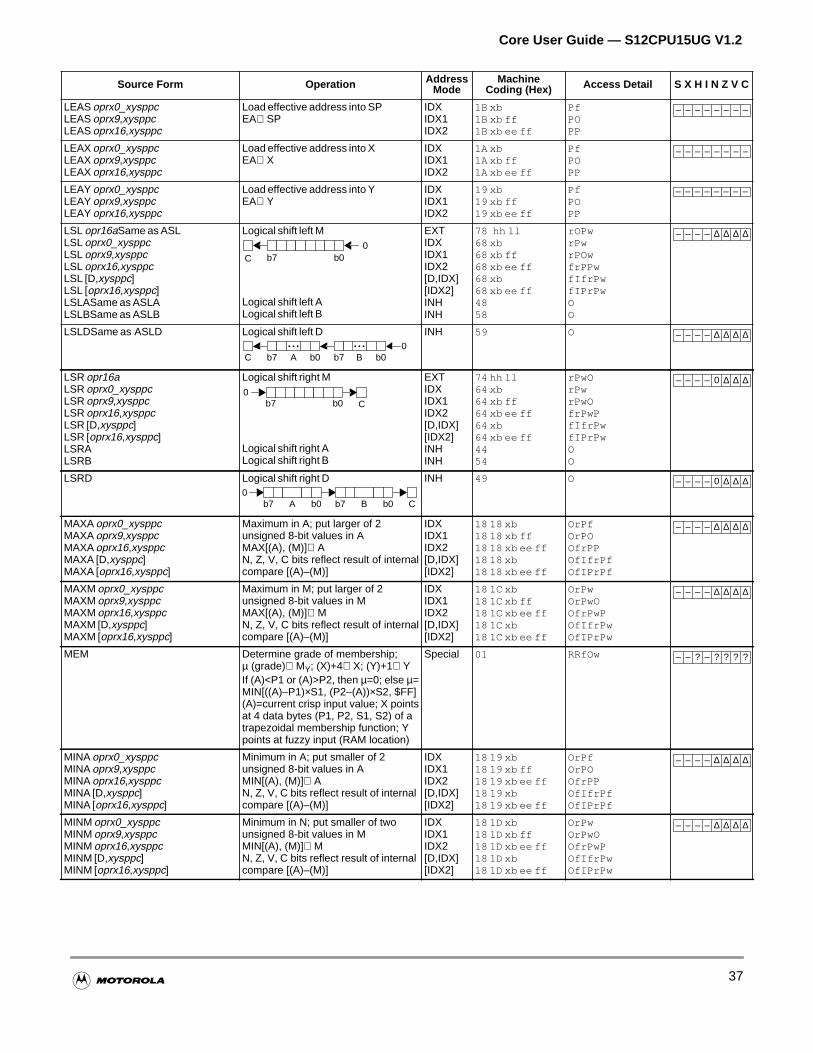
Core User Guide — S12CPU15UG V1.2
LEAS oprx0_xysppcLEAS oprx9,xysppcLEAS oprx16,xysppc
Load effective address into SPEA⇒SP
IDXIDX1IDX2
1B xb1B xb ff1B xb ee ff
PfPOPP
LEAX oprx0_xysppcLEAX oprx9,xysppcLEAX oprx16,xysppc
Load effective address into XEA⇒X
IDXIDX1IDX2
1A xb1A xb ff1A xb ee ff
PfPOPP
LEAY oprx0_xysppcLEAY oprx9,xysppcLEAY oprx16,xysppc
Load effective address into YEA⇒Y
IDXIDX1IDX2
19 xb19 xb ff19 xb ee ff
PfPOPP
LSL opr16aSame as ASLLSL oprx0_xysppcLSL oprx9,xysppcLSL oprx16,xysppcLSL [D,xysppc]LSL [oprx16,xysppc]LSLASame as ASLALSLBSame as ASLB
Logical shift left M
Logical shift left ALogical shift left B
EXTIDXIDX1IDX2[D,IDX][IDX2]INHINH
78 hh ll68 xb68 xb ff68 xb ee ff68 xb68 xb ee ff4858
rOPwrPwrPOwfrPPwfIfrPwfIPrPwOO
LSLDSame as ASLD Logical shift left D INH 59 O
LSR opr16aLSR oprx0_xysppcLSR oprx9,xysppcLSR oprx16,xysppcLSR [D,xysppc]LSR [oprx16,xysppc]LSRALSRB
Logical shift right M
Logical shift right ALogical shift right B
EXTIDXIDX1IDX2[D,IDX][IDX2]INHINH
74 hh ll64 xb64 xb ff64 xb ee ff64 xb64 xb ee ff4454
rPwOrPwrPwOfrPwPfIfrPwfIPrPwOO
LSRD Logical shift right D INH 49 O
MAXA oprx0_xysppcMAXA oprx9,xysppcMAXA oprx16,xysppcMAXA [D,xysppc]MAXA [oprx16,xysppc]
Maximum in A; put larger of 2unsigned 8-bit values in AMAX[(A), (M)]⇒AN, Z, V, C bits reflect result of internalcompare [(A)–(M)]
IDXIDX1IDX2[D,IDX][IDX2]
18 18 xb18 18 xb ff18 18 xb ee ff18 18 xb18 18 xb ee ff
OrPfOrPOOfrPPOfIfrPfOfIPrPf
MAXM oprx0_xysppcMAXM oprx9,xysppcMAXM oprx16,xysppcMAXM [D,xysppc]MAXM [oprx16,xysppc]
Maximum in M; put larger of 2unsigned 8-bit values in MMAX[(A), (M)]⇒MN, Z, V, C bits reflect result of internalcompare [(A)–(M)]
IDXIDX1IDX2[D,IDX][IDX2]
18 1C xb18 1C xb ff18 1C xb ee ff18 1C xb18 1C xb ee ff
OrPwOrPwOOfrPwPOfIfrPwOfIPrPw
MEM Determine grade of membership;µ (grade)⇒MY; (X)+4⇒X; (Y)+1⇒YIf (A)<P1 or (A)>P2, then µ=0; else µ=MIN[((A)–P1)×S1, (P2–(A))×S2, $FF](A)=current crisp input value; X pointsat 4 data bytes (P1, P2, S1, S2) of atrapezoidal membership function; Ypoints at fuzzy input (RAM location)
Special 01 RRfOw
MINA oprx0_xysppcMINA oprx9,xysppcMINA oprx16,xysppcMINA [D,xysppc]MINA [oprx16,xysppc]
Minimum in A; put smaller of 2unsigned 8-bit values in AMIN[(A), (M)]⇒AN, Z, V, C bits reflect result of internalcompare [(A)–(M)]
IDXIDX1IDX2[D,IDX][IDX2]
18 19 xb18 19 xb ff18 19 xb ee ff18 19 xb18 19 xb ee ff
OrPfOrPOOfrPPOfIfrPfOfIPrPf
MINM oprx0_xysppcMINM oprx9,xysppcMINM oprx16,xysppcMINM [D,xysppc]MINM [oprx16,xysppc]
Minimum in N; put smaller of twounsigned 8-bit values in MMIN[(A), (M)]⇒MN, Z, V, C bits reflect result of internalcompare [(A)–(M)]
IDXIDX1IDX2[D,IDX][IDX2]
18 1D xb18 1D xb ff18 1D xb ee ff18 1D xb18 1D xb ee ff
OrPwOrPwOOfrPwPOfIfrPwOfIPrPw
Source Form Operation AddressMode
MachineCoding (Hex) Access Detail S X H I N Z V C
– – – – – – – –
– – – – – – – –
– – – – – – – –
C0
b7 b0
– – – – ∆ ∆ ∆ ∆
C0
b7 b0A Bb7b0• • • • • •
– – – – ∆ ∆ ∆ ∆
C0
b7 b0
– – – – 0 ∆ ∆ ∆
Cb7 b0A Bb7b00
– – – – 0 ∆ ∆ ∆
– – – – ∆ ∆ ∆ ∆
– – – – ∆ ∆ ∆ ∆
– – ? – ? ? ? ?
– – – – ∆ ∆ ∆ ∆
– – – – ∆ ∆ ∆ ∆
37
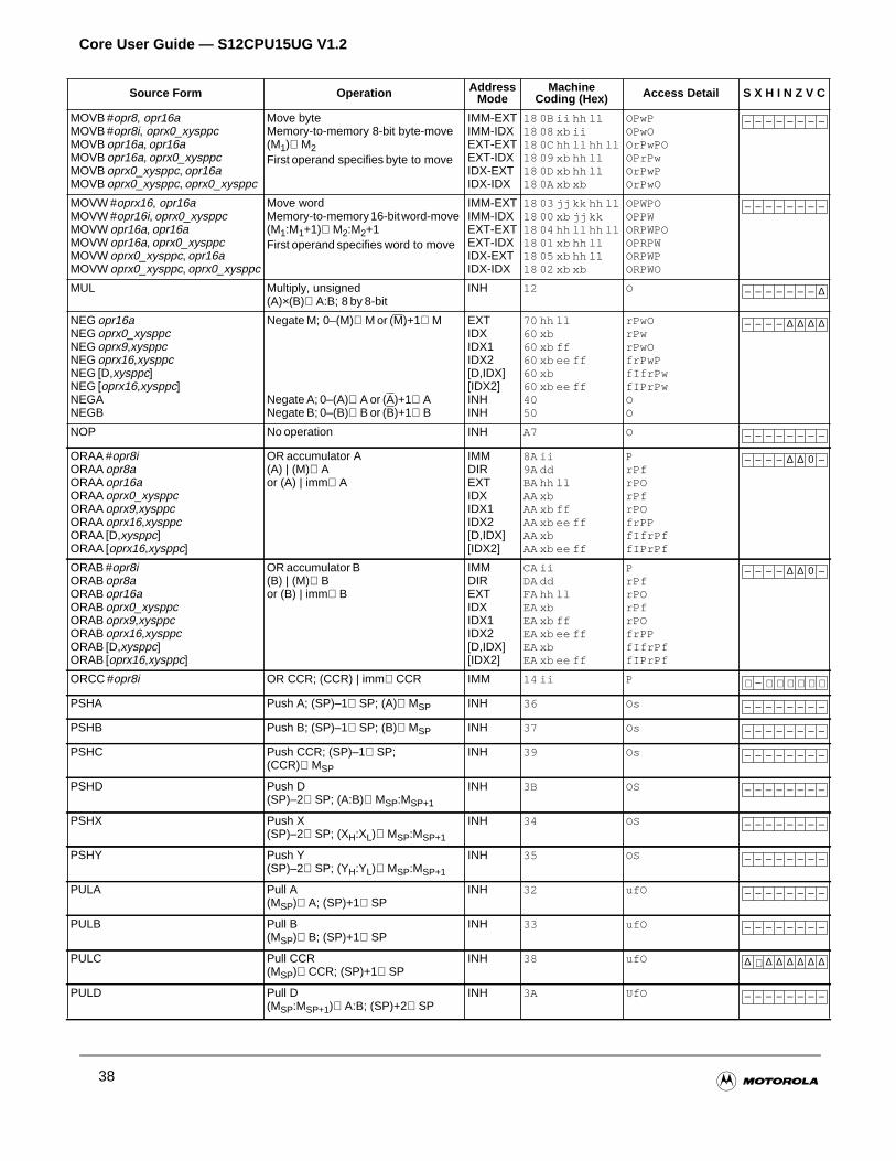
Core User Guide — S12CPU15UG V1.2
MOVB #opr8, opr16aMOVB #opr8i, oprx0_xysppcMOVB opr16a, opr16aMOVB opr16a, oprx0_xysppcMOVB oprx0_xysppc, opr16aMOVB oprx0_xysppc, oprx0_xysppc
Move byteMemory-to-memory 8-bit byte-move(M1)⇒M2First operand specifies byte to move
IMM-EXTIMM-IDXEXT-EXTEXT-IDXIDX-EXTIDX-IDX
18 0B ii hh ll18 08 xb ii18 0C hh ll hh ll18 09 xb hh ll18 0D xb hh ll18 0A xb xb
OPwPOPwOOrPwPOOPrPwOrPwPOrPwO
MOVW #oprx16, opr16aMOVW #opr16i, oprx0_xysppcMOVW opr16a, opr16aMOVW opr16a, oprx0_xysppcMOVW oprx0_xysppc, opr16aMOVW oprx0_xysppc, oprx0_xysppc
Move wordMemory-to-memory16-bitword-move(M1:M1+1)⇒M2:M2+1First operand specifies word to move
IMM-EXTIMM-IDXEXT-EXTEXT-IDXIDX-EXTIDX-IDX
18 03 jj kk hh ll18 00 xb jj kk18 04 hh ll hh ll18 01 xb hh ll18 05 xb hh ll18 02 xb xb
OPWPOOPPWORPWPOOPRPWORPWPORPWO
MUL Multiply, unsigned(A)×(B)⇒A:B; 8 by 8-bit
INH 12 O
NEG opr16aNEG oprx0_xysppcNEG oprx9,xysppcNEG oprx16,xysppcNEG [D,xysppc]NEG [oprx16,xysppc]NEGANEGB
Negate M; 0–(M)⇒M or (M)+1⇒M
Negate A; 0–(A)⇒A or (A)+1⇒ANegate B; 0–(B)⇒B or (B)+1⇒B
EXTIDXIDX1IDX2[D,IDX][IDX2]INHINH
70 hh ll60 xb60 xb ff60 xb ee ff60 xb60 xb ee ff4050
rPwOrPwrPwOfrPwPfIfrPwfIPrPwOO
NOP No operation INH A7 O
ORAA #opr8iORAA opr8aORAA opr16aORAA oprx0_xysppcORAA oprx9,xysppcORAA oprx16,xysppcORAA [D,xysppc]ORAA [oprx16,xysppc]
OR accumulator A(A) | (M)⇒Aor (A) | imm⇒A
IMMDIREXTIDXIDX1IDX2[D,IDX][IDX2]
8A ii9A ddBA hh llAA xbAA xb ffAA xb ee ffAA xbAA xb ee ff
PrPfrPOrPfrPOfrPPfIfrPffIPrPf
ORAB #opr8iORAB opr8aORAB opr16aORAB oprx0_xysppcORAB oprx9,xysppcORAB oprx16,xysppcORAB [D,xysppc]ORAB [oprx16,xysppc]
OR accumulator B(B) | (M)⇒Bor (B) | imm⇒B
IMMDIREXTIDXIDX1IDX2[D,IDX][IDX2]
CA iiDA ddFA hh llEA xbEA xb ffEA xb ee ffEA xbEA xb ee ff
PrPfrPOrPfrPOfrPPfIfrPffIPrPf
ORCC #opr8i OR CCR; (CCR) | imm⇒CCR IMM 14 ii P
PSHA Push A; (SP)–1⇒SP; (A)⇒MSP INH 36 Os
PSHB Push B; (SP)–1⇒SP; (B)⇒MSP INH 37 Os
PSHC Push CCR; (SP)–1⇒SP;(CCR)⇒MSP
INH 39 Os
PSHD Push D(SP)–2⇒SP; (A:B)⇒MSP:MSP+1
INH 3B OS
PSHX Push X(SP)–2⇒SP; (XH:XL)⇒MSP:MSP+1
INH 34 OS
PSHY Push Y(SP)–2⇒SP; (YH:YL)⇒MSP:MSP+1
INH 35 OS
PULA Pull A(MSP)⇒A; (SP)+1⇒SP
INH 32 ufO
PULB Pull B(MSP)⇒B; (SP)+1⇒SP
INH 33 ufO
PULC Pull CCR(MSP)⇒CCR; (SP)+1⇒SP
INH 38 ufO
PULD Pull D(MSP:MSP+1)⇒A:B; (SP)+2⇒SP
INH 3A UfO
Source Form Operation AddressMode
MachineCoding (Hex) Access Detail S X H I N Z V C
– – – – – – – –
– – – – – – – –
– – – – – – – ∆
– – – – ∆ ∆ ∆ ∆
– – – – – – – –
– – – – ∆ ∆ 0 –
– – – – ∆ ∆ 0 –
⇑ – ⇑ ⇑ ⇑ ⇑ ⇑ ⇑
– – – – – – – –
– – – – – – – –
– – – – – – – –
– – – – – – – –
– – – – – – – –
– – – – – – – –
– – – – – – – –
– – – – – – – –
∆ ⇓ ∆ ∆ ∆ ∆ ∆ ∆
– – – – – – – –
38
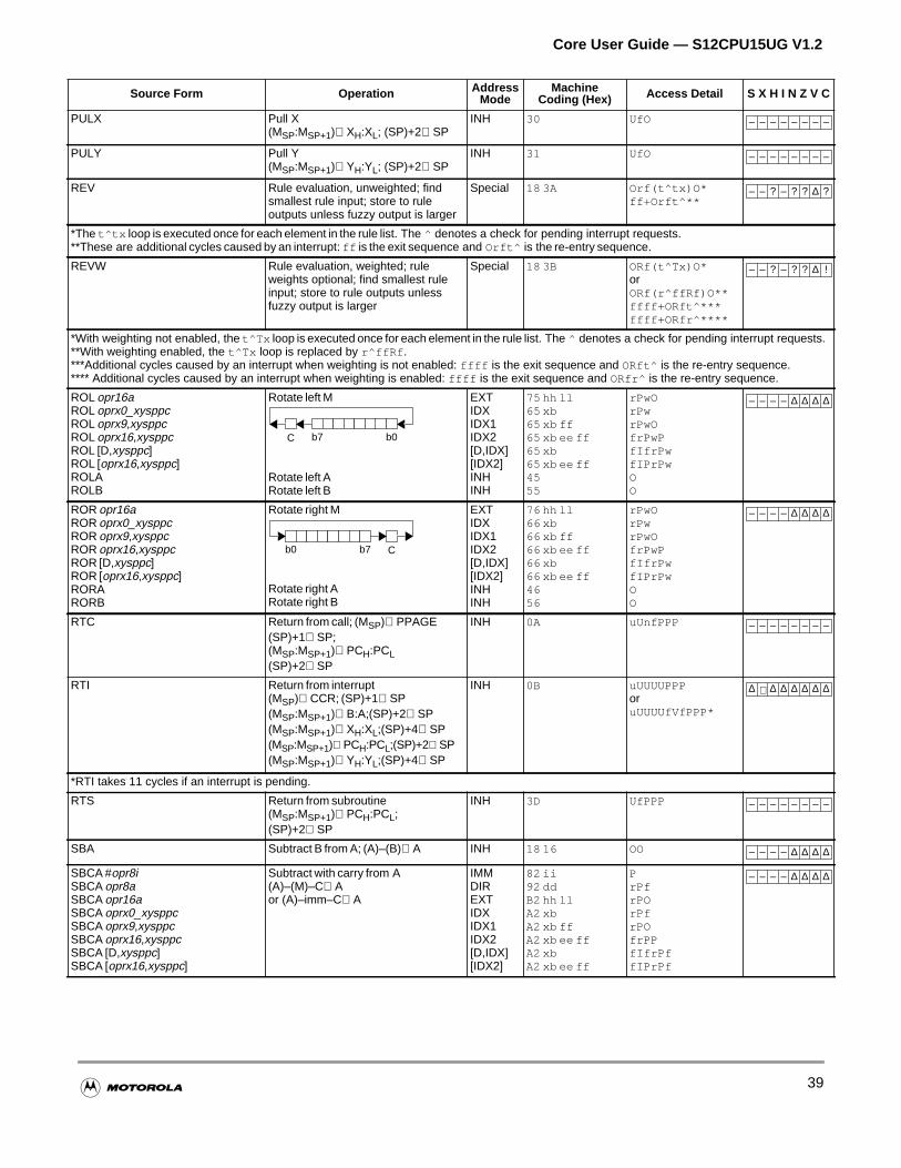
Core User Guide — S12CPU15UG V1.2
PULX Pull X(MSP:MSP+1)⇒XH:XL; (SP)+2⇒SP
INH 30 UfO
PULY Pull Y(MSP:MSP+1)⇒YH:YL; (SP)+2⇒SP
INH 31 UfO
REV Rule evaluation, unweighted; findsmallest rule input; store to ruleoutputs unless fuzzy output is larger
Special 18 3A Orf(t^tx)O*ff+Orft^**
*The t^tx loop is executed once for each element in the rule list. The ^ denotes a check for pending interrupt requests.**These are additional cycles caused by an interrupt: ff is the exit sequence and Orft^ is the re-entry sequence.
REVW Rule evaluation, weighted; ruleweights optional; find smallest ruleinput; store to rule outputs unlessfuzzy output is larger
Special 18 3B ORf(t^Tx)O*orORf(r^ffRf)O**ffff+ORft^***ffff+ORfr^****
*With weighting not enabled, the t^Tx loop is executed once for each element in the rule list. The ^ denotes a check for pending interrupt requests.**With weighting enabled, the t^Tx loop is replaced by r^ffRf .***Additional cycles caused by an interrupt when weighting is not enabled: ffff is the exit sequence and ORft^ is the re-entry sequence.**** Additional cycles caused by an interrupt when weighting is enabled: ffff is the exit sequence and ORfr^ is the re-entry sequence.
ROL opr16aROL oprx0_xysppcROL oprx9,xysppcROL oprx16,xysppcROL [D,xysppc]ROL [oprx16,xysppc]ROLAROLB
Rotate left M
Rotate left ARotate left B
EXTIDXIDX1IDX2[D,IDX][IDX2]INHINH
75 hh ll65 xb65 xb ff65 xb ee ff65 xb65 xb ee ff4555
rPwOrPwrPwOfrPwPfIfrPwfIPrPwOO
ROR opr16aROR oprx0_xysppcROR oprx9,xysppcROR oprx16,xysppcROR [D,xysppc]ROR [oprx16,xysppc]RORARORB
Rotate right M
Rotate right ARotate right B
EXTIDXIDX1IDX2[D,IDX][IDX2]INHINH
76 hh ll66 xb66 xb ff66 xb ee ff66 xb66 xb ee ff4656
rPwOrPwrPwOfrPwPfIfrPwfIPrPwOO
RTC Return from call; (MSP)⇒PPAGE(SP)+1⇒SP;(MSP:MSP+1)⇒PCH:PCL(SP)+2⇒SP
INH 0A uUnfPPP
RTI Return from interrupt(MSP)⇒CCR; (SP)+1⇒SP(MSP:MSP+1)⇒B:A;(SP)+2⇒SP(MSP:MSP+1)⇒XH:XL;(SP)+4⇒SP(MSP:MSP+1)⇒PCH:PCL;(SP)+2⇒SP(MSP:MSP+1)⇒YH:YL;(SP)+4⇒SP
INH 0B uUUUUPPPoruUUUUfVfPPP*
*RTI takes 11 cycles if an interrupt is pending.
RTS Return from subroutine(MSP:MSP+1)⇒PCH:PCL;(SP)+2⇒SP
INH 3D UfPPP
SBA Subtract B from A; (A)–(B)⇒A INH 18 16 OO
SBCA #opr8iSBCA opr8aSBCA opr16aSBCA oprx0_xysppcSBCA oprx9,xysppcSBCA oprx16,xysppcSBCA [D,xysppc]SBCA [oprx16,xysppc]
Subtract with carry from A(A)–(M)–C⇒Aor (A)–imm–C⇒A
IMMDIREXTIDXIDX1IDX2[D,IDX][IDX2]
82 ii92 ddB2 hh llA2 xbA2 xb ffA2 xb ee ffA2 xbA2 xb ee ff
PrPfrPOrPfrPOfrPPfIfrPffIPrPf
Source Form Operation AddressMode
MachineCoding (Hex) Access Detail S X H I N Z V C
– – – – – – – –
– – – – – – – –
– – ? – ? ? ∆ ?
– – ? – ? ? ∆ !
C b7 b0
– – – – ∆ ∆ ∆ ∆
Cb7b0
– – – – ∆ ∆ ∆ ∆
– – – – – – – –
∆ ⇓ ∆ ∆ ∆ ∆ ∆ ∆
– – – – – – – –
– – – – ∆ ∆ ∆ ∆
– – – – ∆ ∆ ∆ ∆
39
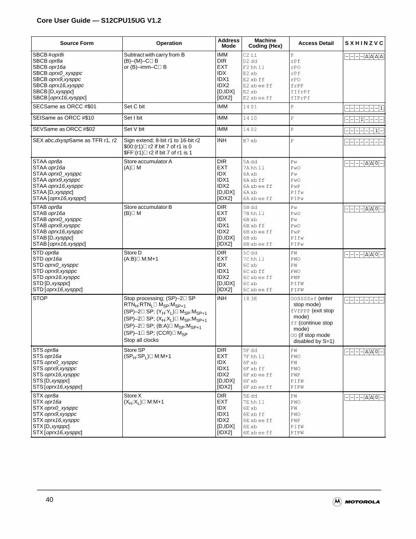
Core User Guide — S12CPU15UG V1.2
SBCB #opr8iSBCB opr8aSBCB opr16aSBCB oprx0_xysppcSBCB oprx9,xysppcSBCB oprx16,xysppcSBCB [D,xysppc]SBCB [oprx16,xysppc]
Subtract with carry from B(B)–(M)–C⇒Bor (B)–imm–C⇒B
IMMDIREXTIDXIDX1IDX2[D,IDX][IDX2]
C2 iiD2 ddF2 hh llE2 xbE2 xb ffE2 xb ee ffE2 xbE2 xb ee ff
PrPfrPOrPfrPOfrPPfIfrPffIPrPf
SECSame as ORCC #$01 Set C bit IMM 14 01 P
SEISame as ORCC #$10 Set I bit IMM 14 10 P
SEVSame as ORCC #$02 Set V bit IMM 14 02 P
SEX abc,dxyspSame as TFR r1, r2 Sign extend; 8-bit r1 to 16-bit r2$00:(r1)⇒r2 if bit 7 of r1 is 0$FF:(r1)⇒r2 if bit 7 of r1 is 1
INH B7 eb P
STAA opr8aSTAA opr16aSTAA oprx0_xysppcSTAA oprx9,xysppcSTAA oprx16,xysppcSTAA [D,xysppc]STAA [oprx16,xysppc]
Store accumulator A(A)⇒M
DIREXTIDXIDX1IDX2[D,IDX][IDX2]
5A dd7A hh ll6A xb6A xb ff6A xb ee ff6A xb6A xb ee ff
PwPwOPwPwOPwPPIfwPIPw
STAB opr8aSTAB opr16aSTAB oprx0_xysppcSTAB oprx9,xysppcSTAB oprx16,xysppcSTAB [D,xysppc]STAB [oprx16,xysppc]
Store accumulator B(B)⇒M
DIREXTIDXIDX1IDX2[D,IDX][IDX2]
5B dd7B hh ll6B xb6B xb ff6B xb ee ff6B xb6B xb ee ff
PwPwOPwPwOPwPPIfwPIPw
STD opr8aSTD opr16aSTD oprx0_xysppcSTD oprx9,xysppcSTD oprx16,xysppcSTD [D,xysppc]STD [oprx16,xysppc]
Store D(A:B)⇒M:M+1
DIREXTIDXIDX1IDX2[D,IDX][IDX2]
5C dd7C hh ll6C xb6C xb ff6C xb ee ff6C xb6C xb ee ff
PWPWOPWPWOPWPPIfWPIPW
STOP Stop processing; (SP)–2⇒SPRTNH:RTNL⇒MSP:MSP+1(SP)–2⇒SP; (YH:YL)⇒MSP:MSP+1(SP)–2⇒SP; (XH:XL)⇒MSP:MSP+1(SP)–2⇒SP; (B:A)⇒MSP:MSP+1(SP)–1⇒SP; (CCR)⇒MSPStop all clocks
INH 18 3E OOSSSSsf (enterstop mode)
fVfPPP (exit stopmode)
ff (continue stopmode)
OO (if stop modedisabled by S=1)
STS opr8aSTS opr16aSTS oprx0_xysppcSTS oprx9,xysppcSTS oprx16,xysppcSTS [D,xysppc]STS [oprx16,xysppc]
Store SP(SPH:SPL)⇒M:M+1
DIREXTIDXIDX1IDX2[D,IDX][IDX2]
5F dd7F hh ll6F xb6F xb ff6F xb ee ff6F xb6F xb ee ff
PWPWOPWPWOPWPPIfWPIPW
STX opr8aSTX opr16aSTX oprx0_xysppcSTX oprx9,xysppcSTX oprx16,xysppcSTX [D,xysppc]STX [oprx16,xysppc]
Store X(XH:XL)⇒M:M+1
DIREXTIDXIDX1IDX2[D,IDX][IDX2]
5E dd7E hh ll6E xb6E xb ff6E xb ee ff6E xb6E xb ee ff
PWPWOPWPWOPWPPIfWPIPW
Source Form Operation AddressMode
MachineCoding (Hex) Access Detail S X H I N Z V C
– – – – ∆ ∆ ∆ ∆
– – – – – – – 1
– – – 1 – – – –
– – – – – – 1 –
– – – – – – – –
– – – – ∆ ∆ 0 –
– – – – ∆ ∆ 0 –
– – – – ∆ ∆ 0 –
– – – – – – – –
– – – – ∆ ∆ 0 –
– – – – ∆ ∆ 0 –
40
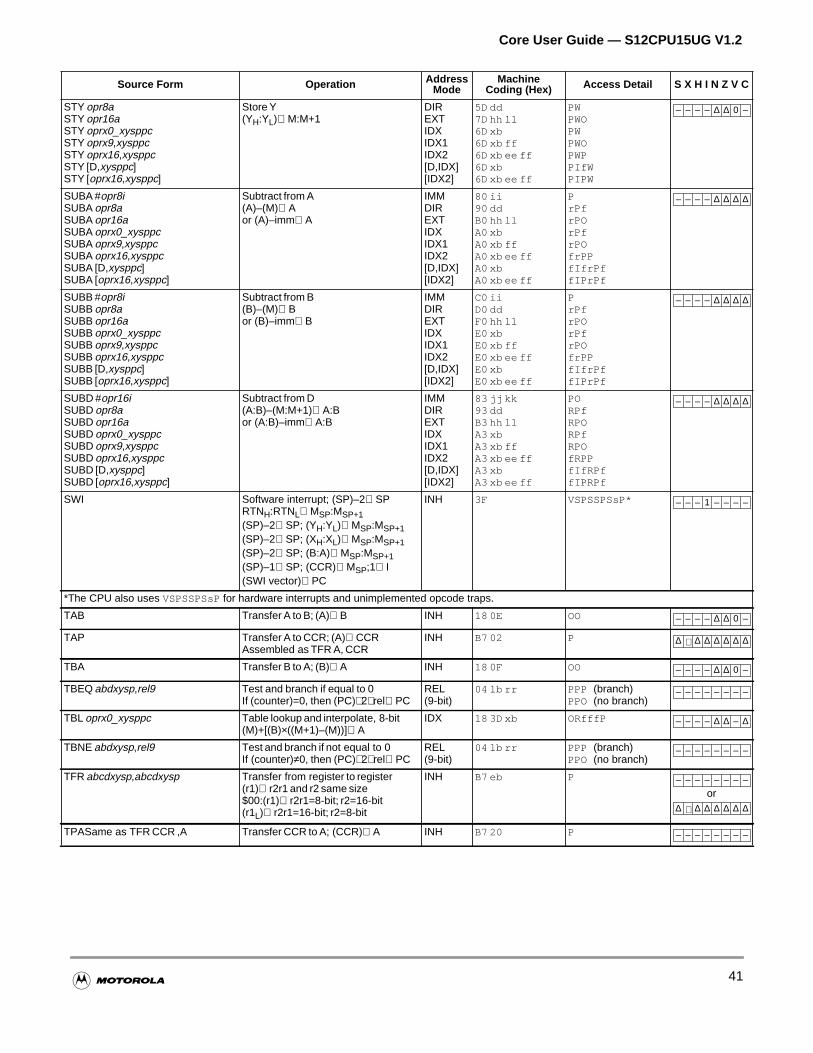
Core User Guide — S12CPU15UG V1.2
STY opr8aSTY opr16aSTY oprx0_xysppcSTY oprx9,xysppcSTY oprx16,xysppcSTY [D,xysppc]STY [oprx16,xysppc]
Store Y(YH:YL)⇒M:M+1
DIREXTIDXIDX1IDX2[D,IDX][IDX2]
5D dd7D hh ll6D xb6D xb ff6D xb ee ff6D xb6D xb ee ff
PWPWOPWPWOPWPPIfWPIPW
SUBA #opr8iSUBA opr8aSUBA opr16aSUBA oprx0_xysppcSUBA oprx9,xysppcSUBA oprx16,xysppcSUBA [D,xysppc]SUBA [oprx16,xysppc]
Subtract from A(A)–(M)⇒Aor (A)–imm⇒A
IMMDIREXTIDXIDX1IDX2[D,IDX][IDX2]
80 ii90 ddB0 hh llA0 xbA0 xb ffA0 xb ee ffA0 xbA0 xb ee ff
PrPfrPOrPfrPOfrPPfIfrPffIPrPf
SUBB #opr8iSUBB opr8aSUBB opr16aSUBB oprx0_xysppcSUBB oprx9,xysppcSUBB oprx16,xysppcSUBB [D,xysppc]SUBB [oprx16,xysppc]
Subtract from B(B)–(M)⇒Bor (B)–imm⇒B
IMMDIREXTIDXIDX1IDX2[D,IDX][IDX2]
C0 iiD0 ddF0 hh llE0 xbE0 xb ffE0 xb ee ffE0 xbE0 xb ee ff
PrPfrPOrPfrPOfrPPfIfrPffIPrPf
SUBD #opr16iSUBD opr8aSUBD opr16aSUBD oprx0_xysppcSUBD oprx9,xysppcSUBD oprx16,xysppcSUBD [D,xysppc]SUBD [oprx16,xysppc]
Subtract from D(A:B)–(M:M+1)⇒A:Bor (A:B)–imm⇒A:B
IMMDIREXTIDXIDX1IDX2[D,IDX][IDX2]
83 jj kk93 ddB3 hh llA3 xbA3 xb ffA3 xb ee ffA3 xbA3 xb ee ff
PORPfRPORPfRPOfRPPfIfRPffIPRPf
SWI Software interrupt; (SP)–2⇒SPRTNH:RTNL⇒MSP:MSP+1(SP)–2⇒SP; (YH:YL)⇒MSP:MSP+1(SP)–2⇒SP; (XH:XL)⇒MSP:MSP+1(SP)–2⇒SP; (B:A)⇒MSP:MSP+1(SP)–1⇒SP; (CCR)⇒MSP;1⇒I(SWI vector)⇒PC
INH 3F VSPSSPSsP*
*The CPU also uses VSPSSPSsP for hardware interrupts and unimplemented opcode traps.
TAB Transfer A to B; (A)⇒B INH 18 0E OO
TAP Transfer A to CCR; (A)⇒CCRAssembled as TFR A, CCR
INH B7 02 P
TBA Transfer B to A; (B)⇒A INH 18 0F OO
TBEQ abdxysp,rel9 Test and branch if equal to 0If (counter)=0, then (PC)+2+rel⇒PC
REL(9-bit)
04 lb rr PPP (branch)PPO (no branch)
TBL oprx0_xysppc Table lookup and interpolate, 8-bit(M)+[(B)×((M+1)–(M))]⇒A
IDX 18 3D xb ORfffP
TBNE abdxysp,rel9 Test and branch if not equal to 0If (counter)≠0, then (PC)+2+rel⇒PC
REL(9-bit)
04 lb rr PPP (branch)PPO (no branch)
TFR abcdxysp,abcdxysp Transfer from register to register(r1)⇒r2r1 and r2 same size$00:(r1)⇒r2r1=8-bit; r2=16-bit(r1L)⇒r2r1=16-bit; r2=8-bit
INH B7 eb P
or
TPASame as TFR CCR ,A Transfer CCR to A; (CCR)⇒A INH B7 20 P
Source Form Operation AddressMode
MachineCoding (Hex) Access Detail S X H I N Z V C
– – – – ∆ ∆ 0 –
– – – – ∆ ∆ ∆ ∆
– – – – ∆ ∆ ∆ ∆
– – – – ∆ ∆ ∆ ∆
– – – 1 – – – –
– – – – ∆ ∆ 0 –
∆ ⇓ ∆ ∆ ∆ ∆ ∆ ∆
– – – – ∆ ∆ 0 –
– – – – – – – –
– – – – ∆ ∆ – ∆
– – – – – – – –
– – – – – – – –
∆ ⇓ ∆ ∆ ∆ ∆ ∆ ∆
– – – – – – – –
41
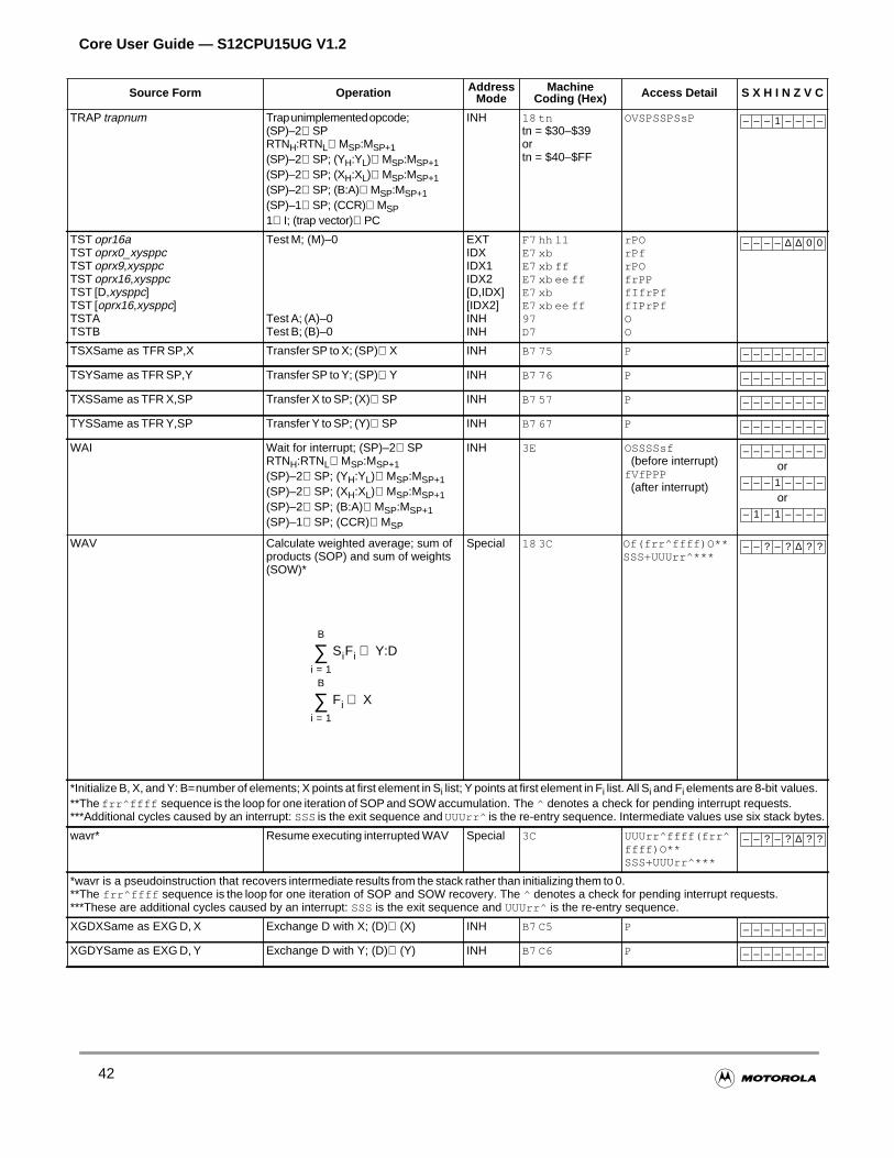
Core User Guide — S12CPU15UG V1.2
TRAP trapnum Trapunimplementedopcode;(SP)–2⇒SPRTNH:RTNL⇒MSP:MSP+1(SP)–2⇒SP; (YH:YL)⇒MSP:MSP+1(SP)–2⇒SP; (XH:XL)⇒MSP:MSP+1(SP)–2⇒SP; (B:A)⇒MSP:MSP+1(SP)–1⇒SP; (CCR)⇒MSP1⇒I; (trap vector)⇒PC
INH 18 tntn = $30–$39ortn = $40–$FF
OVSPSSPSsP
TST opr16aTST oprx0_xysppcTST oprx9,xysppcTST oprx16,xysppcTST [D,xysppc]TST [oprx16,xysppc]TSTATSTB
Test M; (M)–0
Test A; (A)–0Test B; (B)–0
EXTIDXIDX1IDX2[D,IDX][IDX2]INHINH
F7 hh llE7 xbE7 xb ffE7 xb ee ffE7 xbE7 xb ee ff97D7
rPOrPfrPOfrPPfIfrPffIPrPfOO
TSXSame as TFR SP,X Transfer SP to X; (SP)⇒X INH B7 75 P
TSYSame as TFR SP,Y Transfer SP to Y; (SP)⇒Y INH B7 76 P
TXSSame as TFR X,SP Transfer X to SP; (X)⇒SP INH B7 57 P
TYSSame as TFR Y,SP Transfer Y to SP; (Y)⇒SP INH B7 67 P
WAI Wait for interrupt; (SP)–2⇒SPRTNH:RTNL⇒MSP:MSP+1(SP)–2⇒SP; (YH:YL)⇒MSP:MSP+1(SP)–2⇒SP; (XH:XL)⇒MSP:MSP+1(SP)–2⇒SP; (B:A)⇒MSP:MSP+1(SP)–1⇒SP; (CCR)⇒MSP
INH 3E OSSSSsf(before interrupt)
fVfPPP(after interrupt)
or
or
WAV Calculate weighted average; sum ofproducts (SOP) and sum of weights(SOW)*
Special 18 3C Of(frr^ffff)O**SSS+UUUrr^***
*Initialize B, X, and Y: B=number of elements; X points at first element in Si list; Y points at first element in Fi list. All Si and Fi elements are 8-bit values.**The frr^ffff sequence is the loop for one iteration of SOP and SOW accumulation. The ^ denotes a check for pending interrupt requests.***Additional cycles caused by an interrupt: SSSis the exit sequence and UUUrr^ is the re-entry sequence. Intermediate values use six stack bytes.
wavr* Resume executing interrupted WAV Special 3C UUUrr^ffff(frr^ffff)O**SSS+UUUrr^***
*wavr is a pseudoinstruction that recovers intermediate results from the stack rather than initializing them to 0.**The frr^ffff sequence is the loop for one iteration of SOP and SOW recovery. The ^ denotes a check for pending interrupt requests.***These are additional cycles caused by an interrupt: SSS is the exit sequence and UUUrr^ is the re-entry sequence.
XGDXSame as EXG D, X Exchange D with X; (D)⇔(X) INH B7 C5 P
XGDYSame as EXG D, Y Exchange D with Y; (D)⇔(Y) INH B7 C6 P
Source Form Operation AddressMode
MachineCoding (Hex) Access Detail S X H I N Z V C
– – – 1 – – – –
– – – – ∆ ∆ 0 0
– – – – – – – –
– – – – – – – –
– – – – – – – –
– – – – – – – –
– – – – – – – –
– – – 1 – – – –
– 1 – 1 – – – –
Fii 1=
B
∑ X⇒
SiFii 1=
B
∑ Y:D⇒
– – ? – ? ∆ ? ?
– – ? – ? ∆ ? ?
– – – – – – – –
– – – – – – – –
42
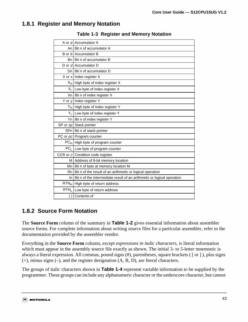
Core User Guide — S12CPU15UG V1.2
to the
ic is
et cannot
1.8.1 Register and Memory Notation
1.8.2 Source Form Notation
TheSource Form column of the summary inTable 1-2 gives essential information about assemblersource forms. For complete information about writing source files for a particular assembler, referdocumentation provided by the assembler vendor.
Everything in theSource Form column,except expressions in italic characters, is literal informationwhich must appear in the assembly source file exactly as shown. The initial 3- to 5-letter mnemonalways a literal expression. All commas, pound signs (#), parentheses, square brackets ( [ or ] ), plus signs(+), minus signs (–), and the register designation (A, B, D), are literal characters.
The groups of italic characters shown inTable 1-4 represent variable information to be supplied by thprogrammer. These groups can include any alphanumeric character or the underscore character, bu
Table 1-3 Register and Memory Notation
A or a Accumulator A
An Bit n of accumulator A
B or b Accumulator B
Bn Bit n of accumulator B
D or d Accumulator D
Dn Bit n of accumulator D
X or x Index register X
XH High byte of index register X
XL Low byte of index register X
Xn Bit n of index register X
Y or y Index register Y
YH High byte of index register Y
YL Low byte of index register Y
Yn Bit n of index register Y
SP or sp Stack pointer
SPn Bit n of stack pointer
PC or pc Program counter
PCH High byte of program counter
PCL Low byte of program counter
CCR or c Condition code register
M Address of 8-bit memory location
Mn Bit n of byte at memory location M
Rn Bit n of the result of an arithmetic or logical operation
In Bit n of the intermediate result of an arithmetic or logical operation
RTNH High byte of return address
RTNL Low byte of return address
( ) Contents of
43
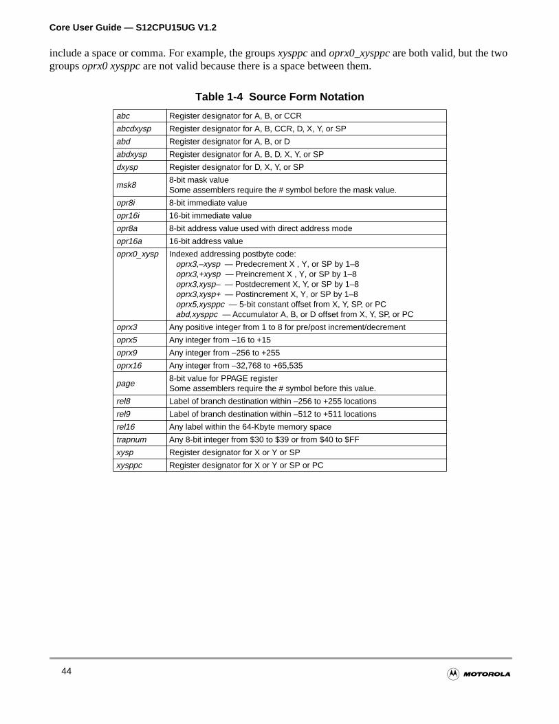
Core User Guide — S12CPU15UG V1.2
include a space or comma. For example, the groupsxysppcandoprx0_xysppcare both valid, but the twogroupsoprx0 xysppc are not valid because there is a space between them.
Table 1-4 Source Form Notation
abc Register designator for A, B, or CCR
abcdxysp Register designator for A, B, CCR, D, X, Y, or SP
abd Register designator for A, B, or D
abdxysp Register designator for A, B, D, X, Y, or SP
dxysp Register designator for D, X, Y, or SP
msk88-bit mask valueSome assemblers require the # symbol before the mask value.
opr8i 8-bit immediate value
opr16i 16-bit immediate value
opr8a 8-bit address value used with direct address mode
opr16a 16-bit address value
oprx0_xysp Indexed addressing postbyte code:oprx3,–xysp — Predecrement X , Y, or SP by 1–8oprx3,+xysp — Preincrement X , Y, or SP by 1–8oprx3,xysp– — Postdecrement X, Y, or SP by 1–8oprx3,xysp+ — Postincrement X, Y, or SP by 1–8oprx5,xysppc — 5-bit constant offset from X, Y, SP, or PCabd,xysppc — Accumulator A, B, or D offset from X, Y, SP, or PC
oprx3 Any positive integer from 1 to 8 for pre/post increment/decrement
oprx5 Any integer from –16 to +15
oprx9 Any integer from –256 to +255
oprx16 Any integer from –32,768 to +65,535
page8-bit value for PPAGE registerSome assemblers require the # symbol before this value.
rel8 Label of branch destination within –256 to +255 locations
rel9 Label of branch destination within –512 to +511 locations
rel16 Any label within the 64-Kbyte memory space
trapnum Any 8-bit integer from $30 to $39 or from $40 to $FF
xysp Register designator for X or Y or SP
xysppc Register designator for X or Y or SP or PC
44
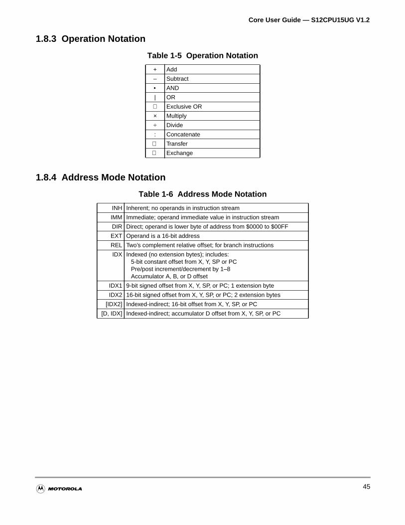
Core User Guide — S12CPU15UG V1.2
1.8.3 Operation Notation
1.8.4 Address Mode Notation
Table 1-5 Operation Notation
+ Add
– Subtract
• AND
| OR
⊕ Exclusive OR
× Multiply
÷ Divide
: Concatenate
⇒ Transfer
⇔ Exchange
Table 1-6 Address Mode Notation
INH Inherent; no operands in instruction stream
IMM Immediate; operand immediate value in instruction stream
DIR Direct; operand is lower byte of address from $0000 to $00FF
EXT Operand is a 16-bit address
REL Two’s complement relative offset; for branch instructions
IDX Indexed (no extension bytes); includes:5-bit constant offset from X, Y, SP or PCPre/post increment/decrement by 1–8Accumulator A, B, or D offset
IDX1 9-bit signed offset from X, Y, SP, or PC; 1 extension byte
IDX2 16-bit signed offset from X, Y, SP, or PC; 2 extension bytes
[IDX2] Indexed-indirect; 16-bit offset from X, Y, SP, or PC
[D, IDX] Indexed-indirect; accumulator D offset from X, Y, SP, or PC
45
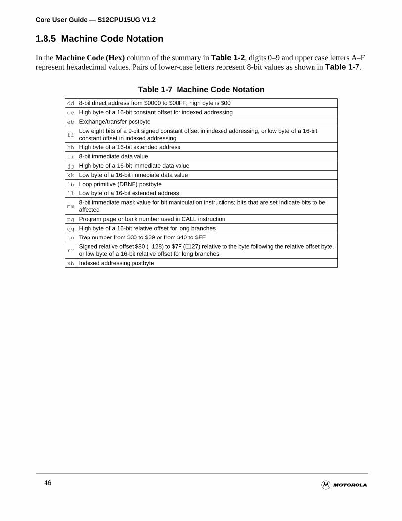
Core User Guide — S12CPU15UG V1.2
1.8.5 Machine Code Notation
In theMachine Code (Hex)column of the summary inTable 1-2 , digits 0–9 and upper case letters A–Frepresent hexadecimal values. Pairs of lower-case letters represent 8-bit values as shown inTable 1-7 .
Table 1-7 Machine Code Notation
dd 8-bit direct address from $0000 to $00FF; high byte is $00
ee High byte of a 16-bit constant offset for indexed addressing
eb Exchange/transfer postbyte
ffLow eight bits of a 9-bit signed constant offset in indexed addressing, or low byte of a 16-bitconstant offset in indexed addressing
hh High byte of a 16-bit extended address
ii 8-bit immediate data value
jj High byte of a 16-bit immediate data value
kk Low byte of a 16-bit immediate data value
lb Loop primitive (DBNE) postbyte
ll Low byte of a 16-bit extended address
mm8-bit immediate mask value for bit manipulation instructions; bits that are set indicate bits to beaffected
pg Program page or bank number used in CALL instruction
qq High byte of a 16-bit relative offset for long branches
tn Trap number from $30 to $39 or from $40 to $FF
rrSigned relative offset $80 (–128) to $7F (+127) relative to the byte following the relative offset byte,or low byte of a 16-bit relative offset for long branches
xb Indexed addressing postbyte
46
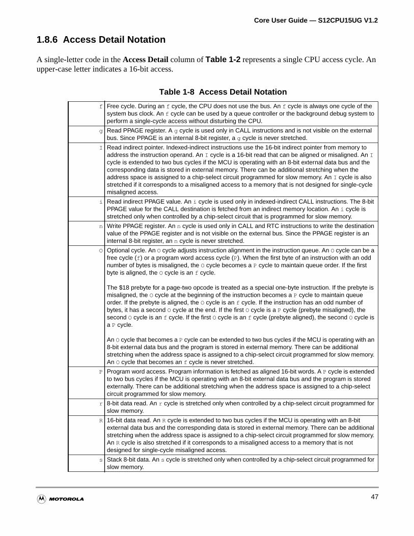
Core User Guide — S12CPU15UG V1.2
n
1.8.6 Access Detail Notation
A single-letter code in theAccess Detailcolumn ofTable 1-2 represents a single CPU access cycle. Aupper-case letter indicates a 16-bit access.
Table 1-8 Access Detail Notation
f Free cycle. During an f cycle, the CPU does not use the bus. An f cycle is always one cycle of thesystem bus clock. An f cycle can be used by a queue controller or the background debug system toperform a single-cycle access without disturbing the CPU.
g Read PPAGE register. A g cycle is used only in CALL instructions and is not visible on the externalbus. Since PPAGE is an internal 8-bit register, a g cycle is never stretched.
I Read indirect pointer. Indexed-indirect instructions use the 16-bit indirect pointer from memory toaddress the instruction operand. An I cycle is a 16-bit read that can be aligned or misaligned. An Icycle is extended to two bus cycles if the MCU is operating with an 8-bit external data bus and thecorresponding data is stored in external memory. There can be additional stretching when theaddress space is assigned to a chip-select circuit programmed for slow memory. An I cycle is alsostretched if it corresponds to a misaligned access to a memory that is not designed for single-cyclemisaligned access.
i Read indirect PPAGE value. An i cycle is used only in indexed-indirect CALL instructions. The 8-bitPPAGE value for the CALL destination is fetched from an indirect memory location. An i cycle isstretched only when controlled by a chip-select circuit that is programmed for slow memory.
n Write PPAGE register. An n cycle is used only in CALL and RTC instructions to write the destinationvalue of the PPAGE register and is not visible on the external bus. Since the PPAGE register is aninternal 8-bit register, an n cycle is never stretched.
O Optional cycle. An Ocycle adjusts instruction alignment in the instruction queue. An Ocycle can be afree cycle (f ) or a program word access cycle (P). When the first byte of an instruction with an oddnumber of bytes is misaligned, the O cycle becomes a P cycle to maintain queue order. If the firstbyte is aligned, the O cycle is an f cycle.
The $18 prebyte for a page-two opcode is treated as a special one-byte instruction. If the prebyte ismisaligned, the O cycle at the beginning of the instruction becomes a P cycle to maintain queueorder. If the prebyte is aligned, the O cycle is an f cycle. If the instruction has an odd number ofbytes, it has a second O cycle at the end. If the first O cycle is a P cycle (prebyte misaligned), thesecond Ocycle is an f cycle. If the first Ocycle is an f cycle (prebyte aligned), the second Ocycle isa P cycle.
An Ocycle that becomes a P cycle can be extended to two bus cycles if the MCU is operating with an8-bit external data bus and the program is stored in external memory. There can be additionalstretching when the address space is assigned to a chip-select circuit programmed for slow memory.An O cycle that becomes an f cycle is never stretched.
P Program word access. Program information is fetched as aligned 16-bit words. A P cycle is extendedto two bus cycles if the MCU is operating with an 8-bit external data bus and the program is storedexternally. There can be additional stretching when the address space is assigned to a chip-selectcircuit programmed for slow memory.
r 8-bit data read. An r cycle is stretched only when controlled by a chip-select circuit programmed forslow memory.
R 16-bit data read. An R cycle is extended to two bus cycles if the MCU is operating with an 8-bitexternal data bus and the corresponding data is stored in external memory. There can be additionalstretching when the address space is assigned to a chip-select circuit programmed for slow memory.An R cycle is also stretched if it corresponds to a misaligned access to a memory that is notdesigned for single-cycle misaligned access.
s Stack 8-bit data. An s cycle is stretched only when controlled by a chip-select circuit programmed forslow memory.
47
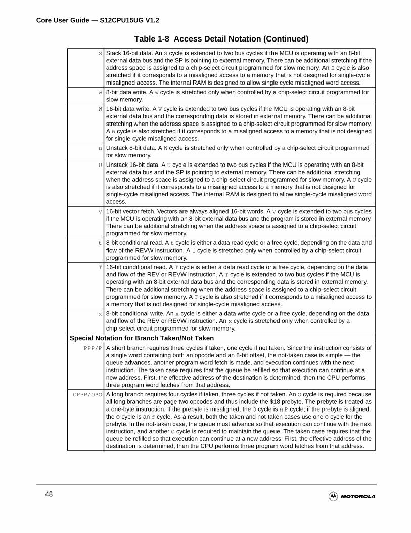
Core User Guide — S12CPU15UG V1.2
S Stack 16-bit data. An S cycle is extended to two bus cycles if the MCU is operating with an 8-bitexternal data bus and the SP is pointing to external memory. There can be additional stretching if theaddress space is assigned to a chip-select circuit programmed for slow memory. An S cycle is alsostretched if it corresponds to a misaligned access to a memory that is not designed for single-cyclemisaligned access. The internal RAM is designed to allow single cycle misaligned word access.
w 8-bit data write. A w cycle is stretched only when controlled by a chip-select circuit programmed forslow memory.
W 16-bit data write. A W cycle is extended to two bus cycles if the MCU is operating with an 8-bitexternal data bus and the corresponding data is stored in external memory. There can be additionalstretching when the address space is assigned to a chip-select circuit programmed for slow memory.A Wcycle is also stretched if it corresponds to a misaligned access to a memory that is not designedfor single-cycle misaligned access.
u Unstack 8-bit data. A W cycle is stretched only when controlled by a chip-select circuit programmedfor slow memory.
U Unstack 16-bit data. A U cycle is extended to two bus cycles if the MCU is operating with an 8-bitexternal data bus and the SP is pointing to external memory. There can be additional stretchingwhen the address space is assigned to a chip-select circuit programmed for slow memory. A U cycleis also stretched if it corresponds to a misaligned access to a memory that is not designed forsingle-cycle misaligned access. The internal RAM is designed to allow single-cycle misaligned wordaccess.
V 16-bit vector fetch. Vectors are always aligned 16-bit words. A V cycle is extended to two bus cyclesif the MCU is operating with an 8-bit external data bus and the program is stored in external memory.There can be additional stretching when the address space is assigned to a chip-select circuitprogrammed for slow memory.
t 8-bit conditional read. A t cycle is either a data read cycle or a free cycle, depending on the data andflow of the REVW instruction. A t cycle is stretched only when controlled by a chip-select circuitprogrammed for slow memory.
T 16-bit conditional read. A T cycle is either a data read cycle or a free cycle, depending on the dataand flow of the REV or REVW instruction. A T cycle is extended to two bus cycles if the MCU isoperating with an 8-bit external data bus and the corresponding data is stored in external memory.There can be additional stretching when the address space is assigned to a chip-select circuitprogrammed for slow memory. A T cycle is also stretched if it corresponds to a misaligned access toa memory that is not designed for single-cycle misaligned access.
x 8-bit conditional write. An x cycle is either a data write cycle or a free cycle, depending on the dataand flow of the REV or REVW instruction. An x cycle is stretched only when controlled by achip-select circuit programmed for slow memory.
Special Notation for Branch Taken/Not TakenPPP/P A short branch requires three cycles if taken, one cycle if not taken. Since the instruction consists of
a single word containing both an opcode and an 8-bit offset, the not-taken case is simple — thequeue advances, another program word fetch is made, and execution continues with the nextinstruction. The taken case requires that the queue be refilled so that execution can continue at anew address. First, the effective address of the destination is determined, then the CPU performsthree program word fetches from that address.
OPPP/OPO A long branch requires four cycles if taken, three cycles if not taken. An O cycle is required becauseall long branches are page two opcodes and thus include the $18 prebyte. The prebyte is treated asa one-byte instruction. If the prebyte is misaligned, the O cycle is a P cycle; if the prebyte is aligned,the O cycle is an f cycle. As a result, both the taken and not-taken cases use one O cycle for theprebyte. In the not-taken case, the queue must advance so that execution can continue with the nextinstruction, and another O cycle is required to maintain the queue. The taken case requires that thequeue be refilled so that execution can continue at a new address. First, the effective address of thedestination is determined, then the CPU performs three program word fetches from that address.
Table 1-8 Access Detail Notation (Continued)
48
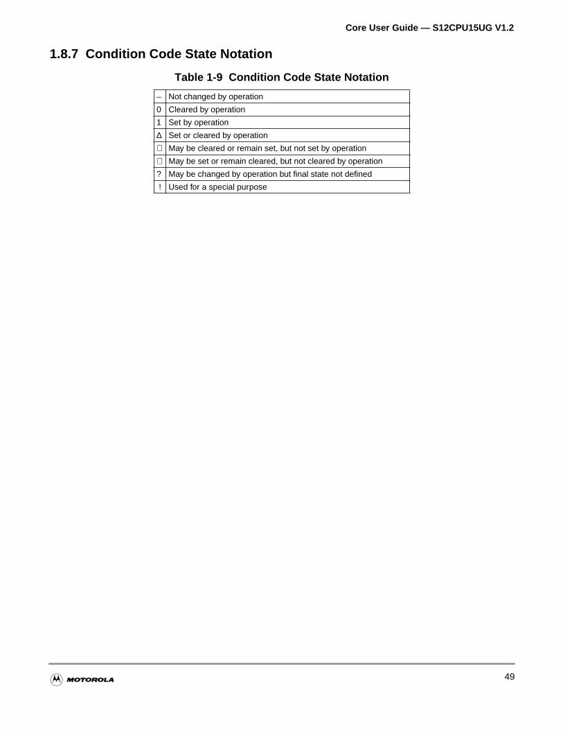
Core User Guide — S12CPU15UG V1.2
1.8.7 Condition Code State Notation
Table 1-9 Condition Code State Notation
– Not changed by operation
0 Cleared by operation
1 Set by operation
∆ Set or cleared by operation
⇓ May be cleared or remain set, but not set by operation
⇑ May be set or remain cleared, but not cleared by operation
? May be changed by operation but final state not defined
! Used for a special purpose
49

Core User Guide — S12CPU15UG V1.2
50

Core User Guide — S12CPU15UG V1.2
Section 2 Nomenclature
This section describes the conventions and notation used to describe the Core operation.
2.1 References
This document uses theSematech Official Dictionary and the JEDEC/EIAReference Guide to LetterSymbols for Semiconductor Devices as references for terminology and symbology.
2.2 Units and Measures
SIU units and abbreviations are used throughout this guide.
2.3 Symbology
The symbols and operators used throughout this guide are shown inTable 2-1 .
2.4 Terminology
Logic level one is a voltage that corresponds to Boolean true (1) state.
Table 2-1 Symbols and Operators
Symbol Function+ Addition
- Subtraction (two’s complement) or negation
* Multiplication
/ Division
> Greater
< Less
= Equal
≥ Equal or greater
≤ Equal or less
Not equal
• AND
+ Inclusive OR (OR)
⊕ Exclusive OR (EOR)
NOT Complementation
: Concatenation
⇒ Transferred
⇔ Exchanged
Tolerance
0b0011 Binary value
0x0F Hexadecimal value
51
Core User Guide — S12CPU15UG V1.2
ls.
gh
at
hest
For
Logic level zero is a voltage that corresponds to Boolean false (0) state.
To set a bit or bits means to establish logic level one on them.
To clear a bit or bits means to establish logic level zero on them.
A signal is an electronic construct whose state or changes in state convey information.
A pin is an external physical connection. The same pin can be used to connect a number of signa
Asserted means that a discrete signal is in active logic state.
• Active low signals change from logic level one to logic level zero.
• Active high signals change from logic level zero to logic level one.
Negated means that an asserted discrete signal changes logic state.
• Active low signals change from logic level zero to logic level one.
• Active high signals change from logic level one to logic level zero.
LSB means least significant bit or bits.MSB means most significant bit or bits. References to low and hibytes or words are spelled out.
Memory and registers usebig-endianordering. The most significant byte (byte 0) of word 0 is locatedaddress 0. Bits within a word are numbered downward from the MSB, bit 15.
Signal, bit field, and control bit mnemonics follow a general numbering scheme:
• A range of mnemonicsis referred to by mnemonic and numbers that define the range, from higto lowest. For example,p_addr[4:0] are lines four to zero of an address bus.
• A single mnemonic stands alone or includes a single numeric designator when appropriate. example,m_rst is a unique mnemonic, whilep_addr15 represents line 15 of an address bus.
52
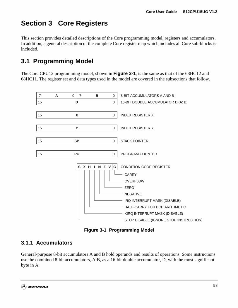
Core User Guide — S12CPU15UG V1.2
lators.cks is
llow.
uctionsficant
Section 3 Core Registers
This section provides detailed descriptions of the Core programming model, registers and accumuIn addition, a general description of the complete Core register map which includes all Core sub-bloincluded.
3.1 Programming Model
The Core CPU12 programming model, shown inFigure 3-1 , is the same as that of the 68HC12 and68HC11. The register set and data types used in the model are covered in the subsections that fo
Figure 3-1 Programming Model
3.1.1 Accumulators
General-purpose 8-bit accumulators A and B hold operands and results of operations. Some instruse the combined 8-bit accumulators, A:B, as a 16-bit double accumulator, D, with the most signibyte in A.
7
15
15
15
15
15
D
X
Y
SP
PC
A B
NS X H I Z V C
0
0
0
0
0
0
70
CONDITION CODE REGISTER
8-BIT ACCUMULATORS A AND B
16-BIT DOUBLE ACCUMULATOR D (A: B)
INDEX REGISTER X
INDEX REGISTER Y
STACK POINTER
PROGRAM COUNTER
STOP DISABLE (IGNORE STOP INSTRUCTION)
CARRY
OVERFLOW
ZERO
NEGATIVE
IRQ INTERRUPT MASK (DISABLE)
HALF-CARRY FOR BCD ARITHMETIC
XIRQ INTERRUPT MASK (DISABLE)
53
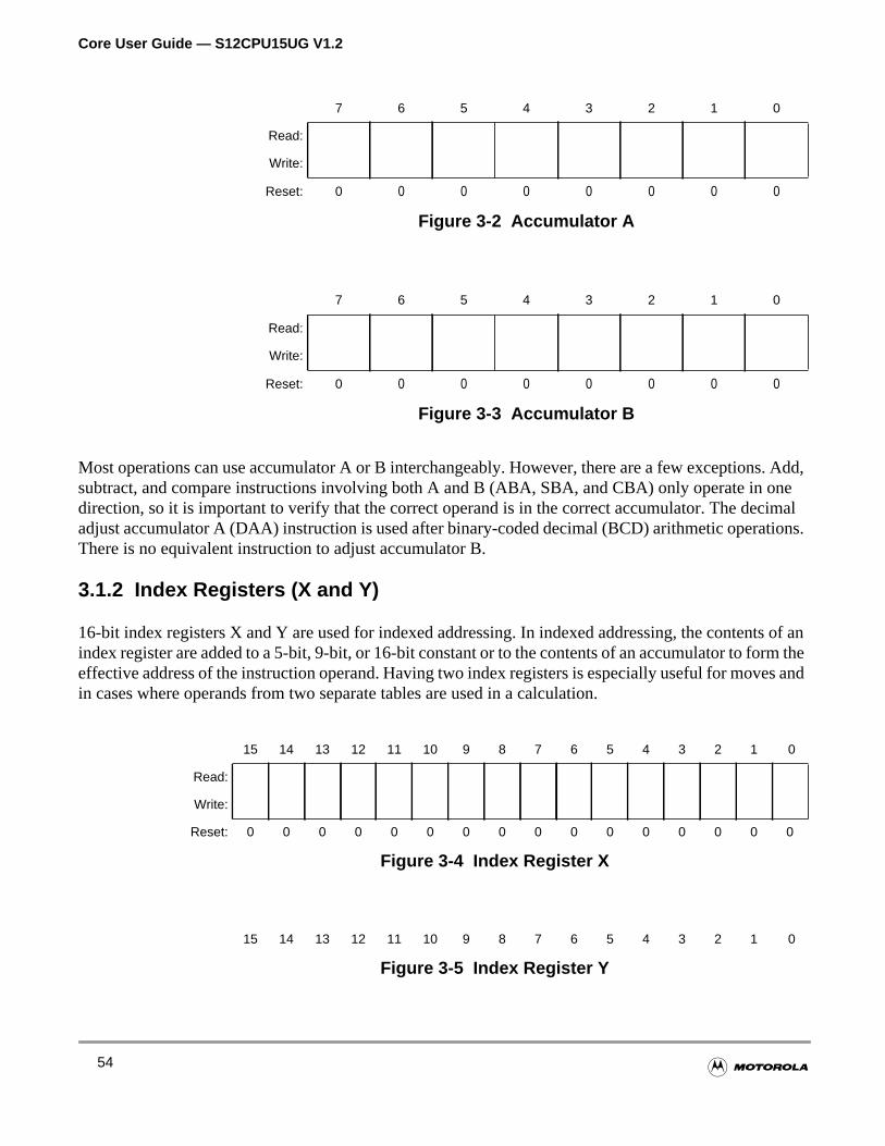
Core User Guide — S12CPU15UG V1.2
. Add,neimal
ions.
s of anrm thes and
Most operations can use accumulator A or B interchangeably. However, there are a few exceptionssubtract, and compare instructions involving both A and B (ABA, SBA, and CBA) only operate in odirection, so it is important to verify that the correct operand is in the correct accumulator. The decadjust accumulator A (DAA) instruction is used after binary-coded decimal (BCD) arithmetic operatThere is no equivalent instruction to adjust accumulator B.
3.1.2 Index Registers (X and Y)
16-bit index registers X and Y are used for indexed addressing. In indexed addressing, the contentindex register are added to a 5-bit, 9-bit, or 16-bit constant or to the contents of an accumulator to foeffective address of the instruction operand. Having two index registers is especially useful for movein cases where operands from two separate tables are used in a calculation.
7 6 5 4 3 2 1 0
Read:
Write:
Reset: 0 0 0 0 0 0 0 0
Figure 3-2 Accumulator A
7 6 5 4 3 2 1 0
Read:
Write:
Reset: 0 0 0 0 0 0 0 0
Figure 3-3 Accumulator B
15 14 13 12 11 10 9 8 7 6 5 4 3 2 1 0
Read:
Write:
Reset: 0 0 0 0 0 0 0 0 0 0 0 0 0 0 0 0
Figure 3-4 Index Register X
15 14 13 12 11 10 9 8 7 6 5 4 3 2 1 0
Figure 3-5 Index Register Y
54
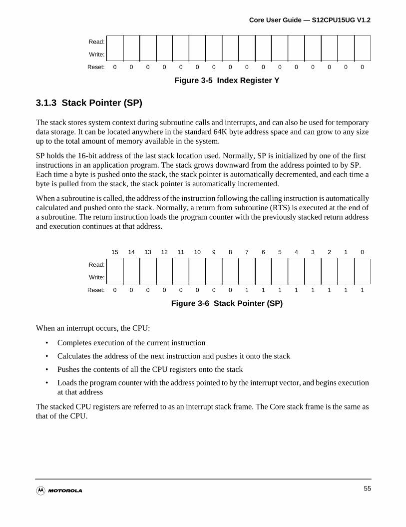
Core User Guide — S12CPU15UG V1.2
poraryany size
e first SP.h time a
icallyend ofddress
cution
same as
3.1.3 Stack Pointer (SP)
The stack stores system context during subroutine calls and interrupts, and can also be used for temdata storage. It can be located anywhere in the standard 64K byte address space and can grow toup to the total amount of memory available in the system.
SP holds the 16-bit address of the last stack location used. Normally, SP is initialized by one of thinstructions in an application program. The stack grows downward from the address pointed to byEach time a byte is pushed onto the stack, the stack pointer is automatically decremented, and eacbyte is pulled from the stack, the stack pointer is automatically incremented.
When a subroutine is called, the address of the instruction following the calling instruction is automatcalculated and pushed onto the stack. Normally, a return from subroutine (RTS) is executed at thea subroutine. The return instruction loads the program counter with the previously stacked return aand execution continues at that address.
When an interrupt occurs, the CPU:
• Completes execution of the current instruction
• Calculates the address of the next instruction and pushes it onto the stack
• Pushes the contents of all the CPU registers onto the stack
• Loads the program counter with the address pointed to by the interrupt vector, and begins exeat that address
The stacked CPU registers are referred to as an interrupt stack frame. The Core stack frame is thethat of the CPU.
Read:
Write:
Reset: 0 0 0 0 0 0 0 0 0 0 0 0 0 0 0 0
15 14 13 12 11 10 9 8 7 6 5 4 3 2 1 0
Read:
Write:
Reset: 0 0 0 0 0 0 0 0 1 1 1 1 1 1 1 1
Figure 3-6 Stack Pointer (SP)
Figure 3-5 Index Register Y
55
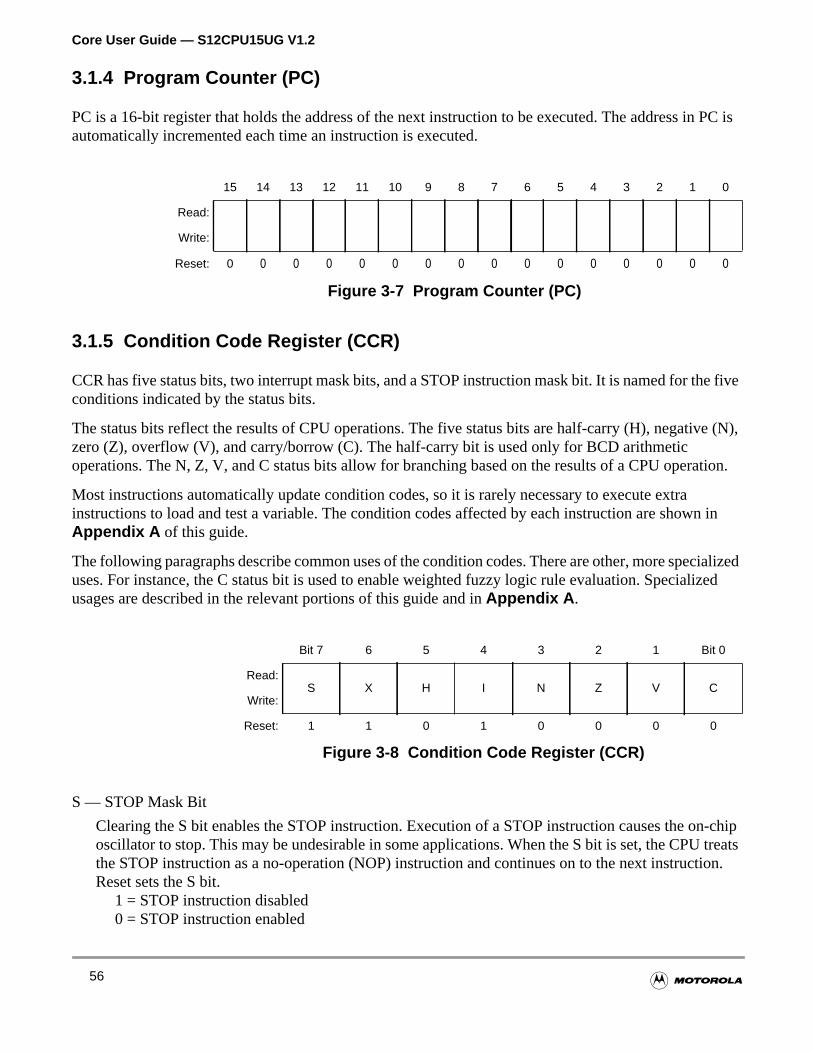
Core User Guide — S12CPU15UG V1.2
n PC is
e five
e (N),
ation.
n in
cializedlized
n-chiptreats
tion.
3.1.4 Program Counter (PC)
PC is a 16-bit register that holds the address of the next instruction to be executed. The address iautomatically incremented each time an instruction is executed.
3.1.5 Condition Code Register (CCR)
CCR has five status bits, two interrupt mask bits, and a STOP instruction mask bit. It is named for thconditions indicated by the status bits.
The status bits reflect the results of CPU operations. The five status bits are half-carry (H), negativzero (Z), overflow (V), and carry/borrow (C). The half-carry bit is used only for BCD arithmeticoperations. The N, Z, V, and C status bits allow for branching based on the results of a CPU oper
Most instructions automatically update condition codes, so it is rarely necessary to execute extrainstructions to load and test a variable. The condition codes affected by each instruction are showAppendix A of this guide.
The following paragraphs describe common uses of the condition codes. There are other, more speuses. For instance, the C status bit is used to enable weighted fuzzy logic rule evaluation. Speciausages are described in the relevant portions of this guide and inAppendix A .
S — STOP Mask Bit
Clearing the S bit enables the STOP instruction. Execution of a STOP instruction causes the ooscillator to stop. This may be undesirable in some applications. When the S bit is set, the CPUthe STOP instruction as a no-operation (NOP) instruction and continues on to the next instrucReset sets the S bit.
1 = STOP instruction disabled0 = STOP instruction enabled
15 14 13 12 11 10 9 8 7 6 5 4 3 2 1 0
Read:
Write:
Reset: 0 0 0 0 0 0 0 0 0 0 0 0 0 0 0 0
Figure 3-7 Program Counter (PC)
Bit 7 6 5 4 3 2 1 Bit 0
Read:S X H I N Z V C
Write:
Reset: 1 1 0 1 0 0 0 0
Figure 3-8 Condition Code Register (CCR)
56
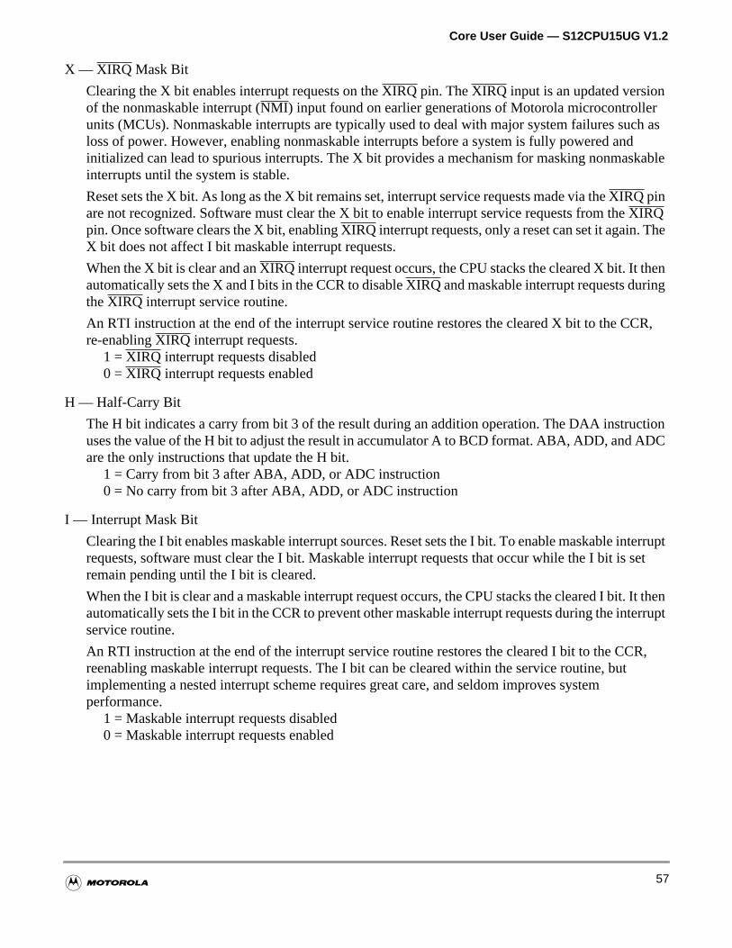
Core User Guide — S12CPU15UG V1.2
ch asdkable
he
eng
CR,
tionDC
terrupt set
It thenerrupt
R,
X — XIRQ Mask Bit
Clearing the X bit enables interrupt requests on theXIRQ pin. TheXIRQ input is an updated versionof the nonmaskable interrupt (NMI) input found on earlier generations of Motorola microcontrollerunits (MCUs). Nonmaskable interrupts are typically used to deal with major system failures suloss of power. However, enabling nonmaskable interrupts before a system is fully powered aninitialized can lead to spurious interrupts. The X bit provides a mechanism for masking nonmasinterrupts until the system is stable.
Reset sets the X bit. As long as the X bit remains set, interrupt service requests made via theXIRQ pinare not recognized. Software must clear the X bit to enable interrupt service requests from theXIRQpin. Once software clears the X bit, enablingXIRQ interrupt requests, only a reset can set it again. TX bit does not affect I bit maskable interrupt requests.
When the X bit is clear and anXIRQ interrupt request occurs, the CPU stacks the cleared X bit. It thautomatically sets the X and I bits in the CCR to disableXIRQ and maskable interrupt requests durintheXIRQ interrupt service routine.
An RTI instruction at the end of the interrupt service routine restores the cleared X bit to the Cre-enablingXIRQ interrupt requests.
1 = XIRQ interrupt requests disabled0 = XIRQ interrupt requests enabled
H — Half-Carry Bit
The H bit indicates a carry from bit 3 of the result during an addition operation. The DAA instrucuses the value of the H bit to adjust the result in accumulator A to BCD format. ABA, ADD, and Aare the only instructions that update the H bit.
1 = Carry from bit 3 after ABA, ADD, or ADC instruction0 = No carry from bit 3 after ABA, ADD, or ADC instruction
I — Interrupt Mask Bit
Clearing the I bit enables maskable interrupt sources. Reset sets the I bit. To enable maskable inrequests, software must clear the I bit. Maskable interrupt requests that occur while the I bit isremain pending until the I bit is cleared.
When the I bit is clear and a maskable interrupt request occurs, the CPU stacks the cleared I bit.automatically sets the I bit in the CCR to prevent other maskable interrupt requests during the intservice routine.
An RTI instruction at the end of the interrupt service routine restores the cleared I bit to the CCreenabling maskable interrupt requests. The I bit can be cleared within the service routine, butimplementing a nested interrupt scheme requires great care, and seldom improves systemperformance.
1 = Maskable interrupt requests disabled0 = Maskable interrupt requests enabled
57
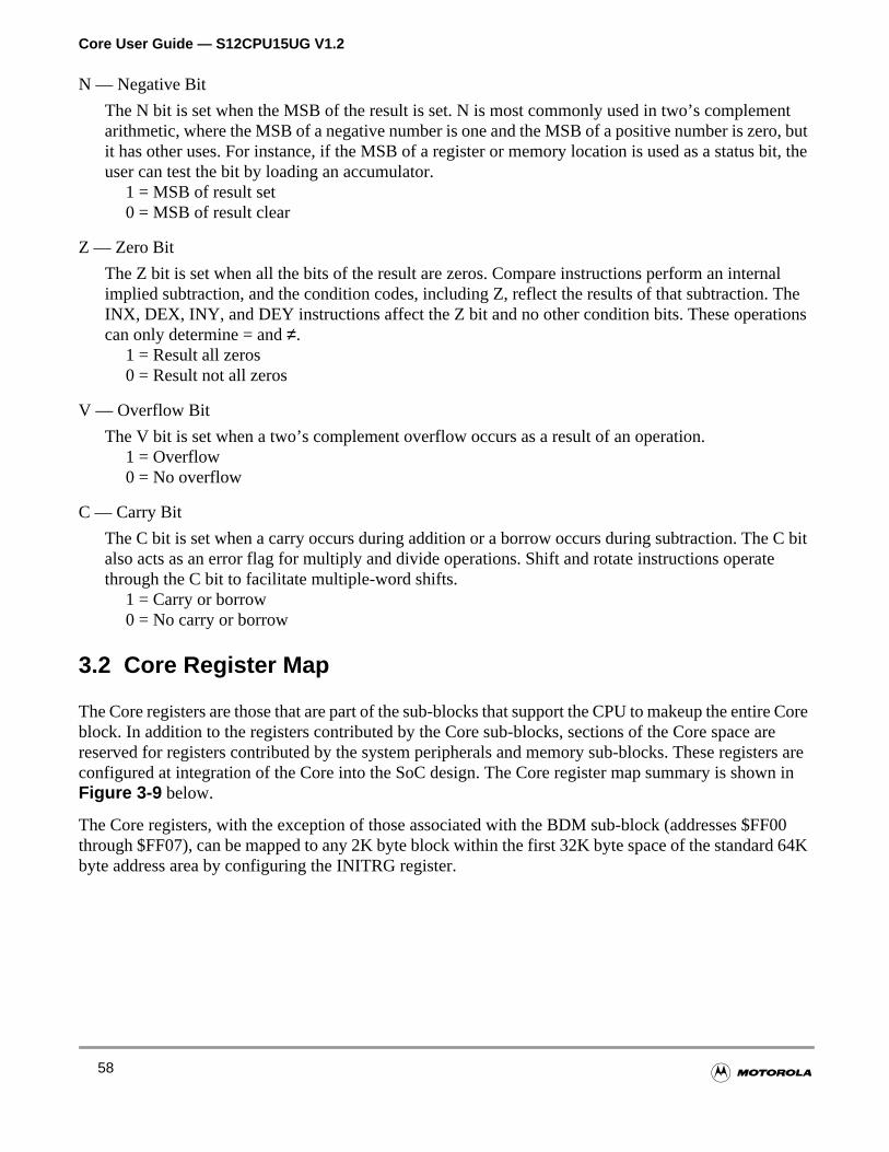
Core User Guide — S12CPU15UG V1.2
ento, butit, the
nal Theions
C bitte
ire Coreareters arewn in
F0064K
N — Negative Bit
The N bit is set when the MSB of the result is set. N is most commonly used in two’s complemarithmetic, where the MSB of a negative number is one and the MSB of a positive number is zerit has other uses. For instance, if the MSB of a register or memory location is used as a status buser can test the bit by loading an accumulator.
1 = MSB of result set0 = MSB of result clear
Z — Zero Bit
The Z bit is set when all the bits of the result are zeros. Compare instructions perform an interimplied subtraction, and the condition codes, including Z, reflect the results of that subtraction.INX, DEX, INY, and DEY instructions affect the Z bit and no other condition bits. These operatcan only determine = and≠.
1 = Result all zeros0 = Result not all zeros
V — Overflow Bit
The V bit is set when a two’s complement overflow occurs as a result of an operation.1 = Overflow0 = No overflow
C — Carry Bit
The C bit is set when a carry occurs during addition or a borrow occurs during subtraction. Thealso acts as an error flag for multiply and divide operations. Shift and rotate instructions operathrough the C bit to facilitate multiple-word shifts.
1 = Carry or borrow0 = No carry or borrow
3.2 Core Register Map
The Core registers are those that are part of the sub-blocks that support the CPU to makeup the entblock. In addition to the registers contributed by the Core sub-blocks, sections of the Core space reserved for registers contributed by the system peripherals and memory sub-blocks. These regisconfigured at integration of the Core into the SoC design. The Core register map summary is shoFigure 3-9 below.
The Core registers, with the exception of those associated with the BDM sub-block (addresses $Fthrough $FF07), can be mapped to any 2K byte block within the first 32K byte space of the standardbyte address area by configuring the INITRG register.
58
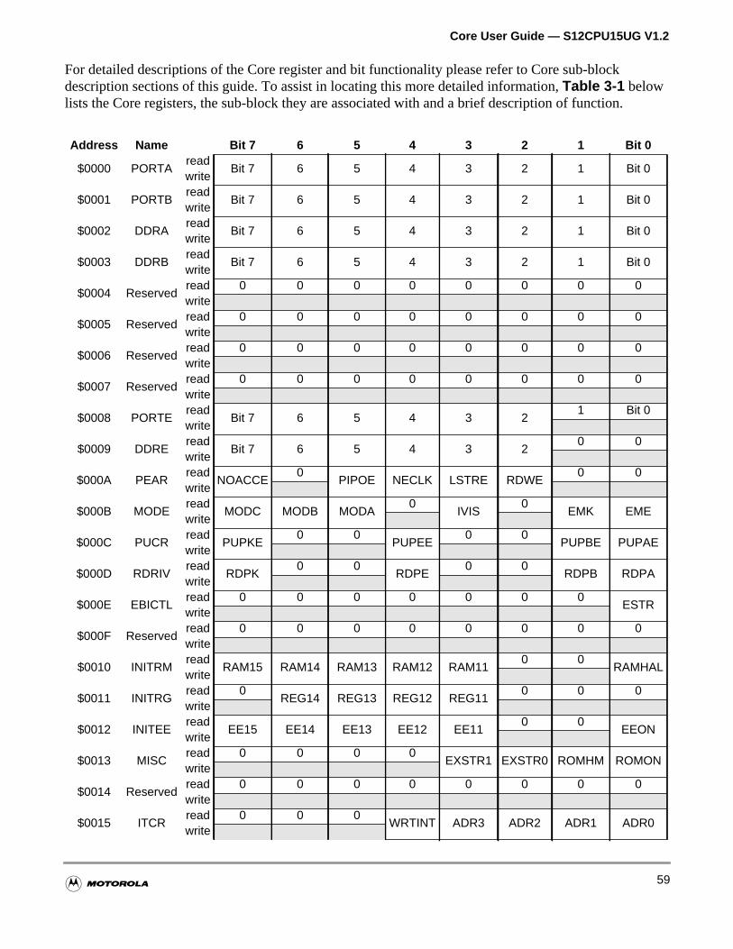
Core User Guide — S12CPU15UG V1.2
For detailed descriptions of the Core register and bit functionality please refer to Core sub-blockdescription sections of this guide. To assist in locating this more detailed information,Table 3-1 belowlists the Core registers, the sub-block they are associated with and a brief description of function.
Address Name Bit 7 6 5 4 3 2 1 Bit 0
$0000 PORTAread
Bit 7 6 5 4 3 2 1 Bit 0write
$0001 PORTBread
Bit 7 6 5 4 3 2 1 Bit 0write
$0002 DDRAread
Bit 7 6 5 4 3 2 1 Bit 0write
$0003 DDRBread
Bit 7 6 5 4 3 2 1 Bit 0write
$0004 Reservedread 0 0 0 0 0 0 0 0write
$0005 Reservedread 0 0 0 0 0 0 0 0write
$0006 Reservedread 0 0 0 0 0 0 0 0write
$0007 Reservedread 0 0 0 0 0 0 0 0write
$0008 PORTEread
Bit 7 6 5 4 3 21 Bit 0
write
$0009 DDREread
Bit 7 6 5 4 3 20 0
write
$000A PEARread
NOACCE0
PIPOE NECLK LSTRE RDWE0 0
write
$000B MODEread
MODC MODB MODA0
IVIS0
EMK EMEwrite
$000C PUCRread
PUPKE0 0
PUPEE0 0
PUPBE PUPAEwrite
$000D RDRIVread
RDPK0 0
RDPE0 0
RDPB RDPAwrite
$000E EBICTLread 0 0 0 0 0 0 0
ESTRwrite
$000F Reservedread 0 0 0 0 0 0 0 0write
$0010 INITRMread
RAM15 RAM14 RAM13 RAM12 RAM110 0
RAMHALwrite
$0011 INITRGread 0
REG14 REG13 REG12 REG110 0 0
write
$0012 INITEEread
EE15 EE14 EE13 EE12 EE110 0
EEONwrite
$0013 MISCread 0 0 0 0
EXSTR1 EXSTR0 ROMHM ROMONwrite
$0014 Reservedread 0 0 0 0 0 0 0 0write
$0015 ITCRread 0 0 0
WRTINT ADR3 ADR2 ADR1 ADR0write
59
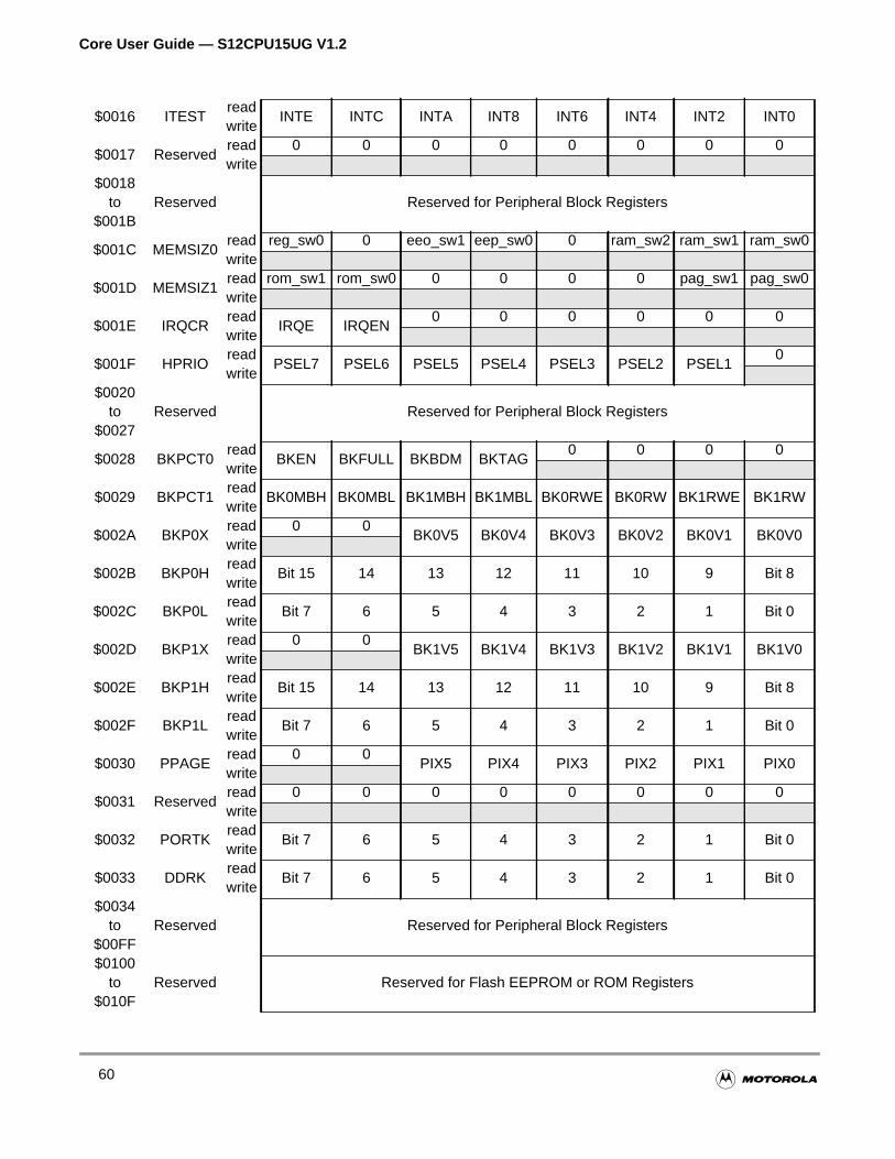
Core User Guide — S12CPU15UG V1.2
$0016 ITESTread
INTE INTC INTA INT8 INT6 INT4 INT2 INT0write
$0017 Reservedread 0 0 0 0 0 0 0 0write
$0018Reserved Reserved for Peripheral Block Registersto
$001B
$001C MEMSIZ0read reg_sw0 0 eeo_sw1 eep_sw0 0 ram_sw2 ram_sw1 ram_sw0write
$001D MEMSIZ1read rom_sw1 rom_sw0 0 0 0 0 pag_sw1 pag_sw0write
$001E IRQCRread
IRQE IRQEN0 0 0 0 0 0
write
$001F HPRIOread
PSEL7 PSEL6 PSEL5 PSEL4 PSEL3 PSEL2 PSEL10
write$0020
Reserved Reserved for Peripheral Block Registersto$0027
$0028 BKPCT0read
BKEN BKFULL BKBDM BKTAG0 0 0 0
write
$0029 BKPCT1read
BK0MBH BK0MBL BK1MBH BK1MBL BK0RWE BK0RW BK1RWE BK1RWwrite
$002A BKP0Xread 0 0
BK0V5 BK0V4 BK0V3 BK0V2 BK0V1 BK0V0write
$002B BKP0Hread
Bit 15 14 13 12 11 10 9 Bit 8write
$002C BKP0Lread
Bit 7 6 5 4 3 2 1 Bit 0write
$002D BKP1Xread 0 0
BK1V5 BK1V4 BK1V3 BK1V2 BK1V1 BK1V0write
$002E BKP1Hread
Bit 15 14 13 12 11 10 9 Bit 8write
$002F BKP1Lread
Bit 7 6 5 4 3 2 1 Bit 0write
$0030 PPAGEread 0 0
PIX5 PIX4 PIX3 PIX2 PIX1 PIX0write
$0031 Reservedread 0 0 0 0 0 0 0 0write
$0032 PORTKread
Bit 7 6 5 4 3 2 1 Bit 0write
$0033 DDRKread
Bit 7 6 5 4 3 2 1 Bit 0write
$0034Reserved Reserved for Peripheral Block Registersto
$00FF$0100
Reserved Reserved for Flash EEPROM or ROM Registersto$010F
60
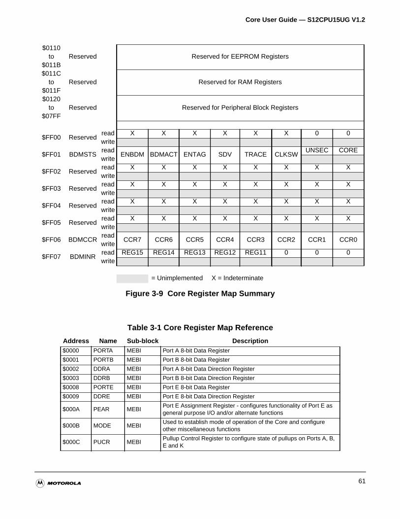
Core User Guide — S12CPU15UG V1.2
Figure 3-9 Core Register Map Summary
$0110Reserved Reserved for EEPROM Registersto
$011B$011C
Reserved Reserved for RAM Registersto$011F$0120
Reserved Reserved for Peripheral Block Registersto$07FF
$FF00 Reservedread X X X X X X 0 0write
$FF01 BDMSTSread
ENBDM BDMACT ENTAG SDV TRACE CLKSWUNSEC CORE
write
$FF02 Reservedread X X X X X X X Xwrite
$FF03 Reservedread X X X X X X X Xwrite
$FF04 Reservedread X X X X X X X Xwrite
$FF05 Reservedread X X X X X X X Xwrite
$FF06 BDMCCRread
CCR7 CCR6 CCR5 CCR4 CCR3 CCR2 CCR1 CCR0write
$FF07 BDMINRread REG15 REG14 REG13 REG12 REG11 0 0 0write
= Unimplemented X = Indeterminate
Table 3-1 Core Register Map Reference
Address Name Sub-block Description$0000 PORTA MEBI Port A 8-bit Data Register
$0001 PORTB MEBI Port B 8-bit Data Register
$0002 DDRA MEBI Port A 8-bit Data Direction Register
$0003 DDRB MEBI Port B 8-bit Data Direction Register
$0008 PORTE MEBI Port E 8-bit Data Register
$0009 DDRE MEBI Port E 8-bit Data Direction Register
$000A PEAR MEBIPort E Assignment Register - configures functionality of Port E asgeneral purpose I/O and/or alternate functions
$000B MODE MEBIUsed to establish mode of operation of the Core and configureother miscellaneous functions
$000C PUCR MEBIPullup Control Register to configure state of pullups on Ports A, B,E and K
61
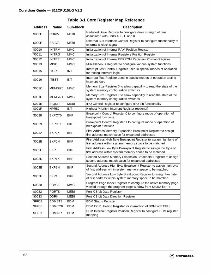
Core User Guide — S12CPU15UG V1.2
$000D RDRIV MEBIReduced Drive Register to configure drive strength of pinsassociated with Ports A, B, E and K
$000E EBICTL MEBIExternal Bus Interface Control Register to configure functionality ofexternal E-clock signal
$0010 INITRM MMC Initialization of Internal RAM Position Register
$0011 INITRG MMC Initialization of Internal Registers Position Register
$0012 INITEE MMC Initialization of Internal EEPROM Registers Position Register
$0013 MISC MMC Miscellaneous Register to configure various system functions
$0015 ITCR INTInterrupt Test Control Register used in special modes of operationfor testing interrupt logic
$0016 ITEST INTInterrupt Test Register used in special modes of operation testinginterrupt logic
$001C MEMSIZ0 MMCMemory Size Register 0 to allow capability to read the state of thesystem memory configuration switches
$001D MEMSIZ1 MMCMemory Size Register 1 to allow capability to read the state of thesystem memory configuration switches
$001E IRQCR MEBI IRQ Control Register to configure IRQ pin functionality
$001F HPRIO INT Highest Priority I Interrupt Register (optional)
$0028 BKPCT0 BKPBreakpoint Control Register 0 to configure mode of operation ofbreakpoint functions
$0029 BKPCT1 BKPBreakpoint Control Register 1 to configure mode of operation ofbreakpoint functions
$002A BKP0X BKPFirst Address Memory Expansion Breakpoint Register to assignfirst address match value for expanded addresses
$002B BKP0H BKPFirst Address High Byte Breakpoint Register to assign high byte offirst address within system memory space to be matched
$002C BKP0L BKPFirst Address Low Byte Breakpoint Register to assign low byte offirst address within system memory space to be matched
$002D BKP1X BKPSecond Address Memory Expansion Breakpoint Register to assignsecond address match value for expanded addresses
$002E BKP1H BKPSecond Address High Byte Breakpoint Register to assign high byteof first address within system memory space to be matched
$002F BKP1L BKPSecond Address Low Byte Breakpoint Register to assign low byteof first address within system memory space to be matched
$0030 PPAGE MMCProgram Page Index Register to configure the active memory pageviewed through the program page window from $8000-$BFFF
$0032 PORTK MEBI Port K 8-bit Data Register
$0033 DDRK MEBI Port K 8-bit Data Direction Register
$FF01 BDMSTS BDM BDM Status Register
$FF06 BDMCCR BDM BDM CCR Holding Register for interaction of BDM with CPU
$FF07 BDMINR BDMBDM Internal Register Position Register to configure BDM registermapping
Table 3-1 Core Register Map Reference
Address Name Sub-block Description
62
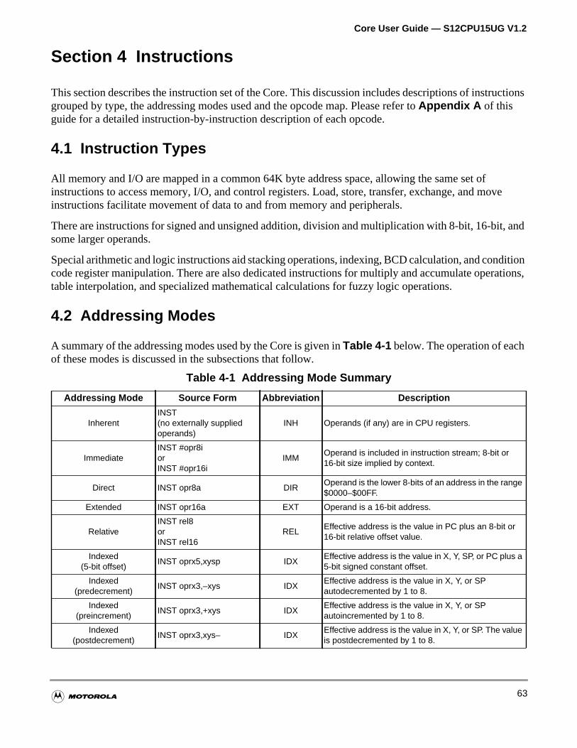
Core User Guide — S12CPU15UG V1.2
ctions
ve
and
ditionations,
Section 4 Instructions
This section describes the instruction set of the Core. This discussion includes descriptions of instrugrouped by type, the addressing modes used and the opcode map. Please refer toAppendix A of thisguide for a detailed instruction-by-instruction description of each opcode.
4.1 Instruction Types
All memory and I/O are mapped in a common 64K byte address space, allowing the same set ofinstructions to access memory, I/O, and control registers. Load, store, transfer, exchange, and moinstructions facilitate movement of data to and from memory and peripherals.
There are instructions for signed and unsigned addition, division and multiplication with 8-bit, 16-bit,some larger operands.
Special arithmetic and logic instructions aid stacking operations, indexing, BCD calculation, and concode register manipulation. There are also dedicated instructions for multiply and accumulate opertable interpolation, and specialized mathematical calculations for fuzzy logic operations.
4.2 Addressing Modes
A summary of the addressing modes used by the Core is given inTable 4-1 below. The operation of eachof these modes is discussed in the subsections that follow.
Table 4-1 Addressing Mode Summary
Addressing Mode Source Form Abbreviation Description
InherentINST(no externally suppliedoperands)
INH Operands (if any) are in CPU registers.
ImmediateINST #opr8iorINST #opr16i
IMMOperand is included in instruction stream; 8-bit or16-bit size implied by context.
Direct INST opr8a DIROperand is the lower 8-bits of an address in the range$0000–$00FF.
Extended INST opr16a EXT Operand is a 16-bit address.
RelativeINST rel8orINST rel16
RELEffective address is the value in PC plus an 8-bit or16-bit relative offset value.
Indexed(5-bit offset)
INST oprx5,xysp IDXEffective address is the value in X, Y, SP, or PC plus a5-bit signed constant offset.
Indexed(predecrement)
INST oprx3,–xys IDXEffective address is the value in X, Y, or SPautodecremented by 1 to 8.
Indexed(preincrement)
INST oprx3,+xys IDXEffective address is the value in X, Y, or SPautoincremented by 1 to 8.
Indexed(postdecrement)
INST oprx3,xys– IDXEffective address is the value in X, Y, or SP. The valueis postdecremented by 1 to 8.
63
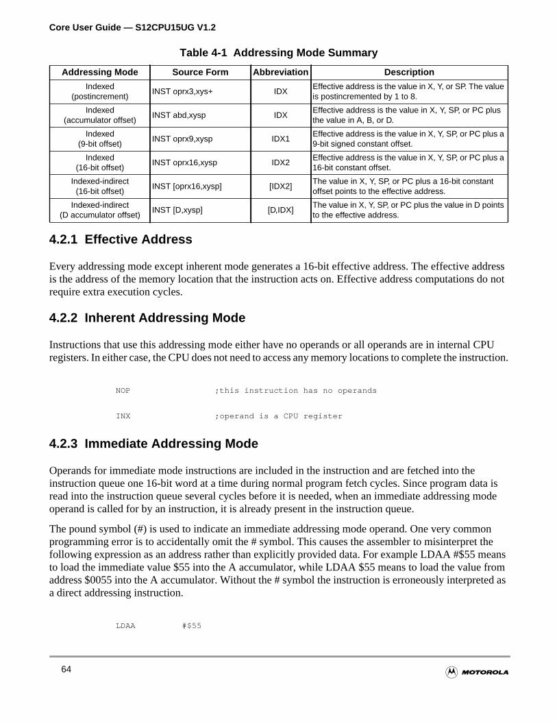
Core User Guide — S12CPU15UG V1.2
address do not
l CPUtruction.
ta is mode
mont theeans fromted as
4.2.1 Effective Address
Every addressing mode except inherent mode generates a 16-bit effective address. The effectiveis the address of the memory location that the instruction acts on. Effective address computationsrequire extra execution cycles.
4.2.2 Inherent Addressing Mode
Instructions that use this addressing mode either have no operands or all operands are in internaregisters. In either case, the CPU does not need to access any memory locations to complete the ins
4.2.3 Immediate Addressing Mode
Operands for immediate mode instructions are included in the instruction and are fetched into theinstruction queue one 16-bit word at a time during normal program fetch cycles. Since program daread into the instruction queue several cycles before it is needed, when an immediate addressingoperand is called for by an instruction, it is already present in the instruction queue.
The pound symbol (#) is used to indicate an immediate addressing mode operand. One very comprogramming error is to accidentally omit the # symbol. This causes the assembler to misinterprefollowing expression as an address rather than explicitly provided data. For example LDAA #$55 mto load the immediate value $55 into the A accumulator, while LDAA $55 means to load the valueaddress $0055 into the A accumulator. Without the # symbol the instruction is erroneously interprea direct addressing instruction.
Indexed(postincrement)
INST oprx3,xys+ IDXEffective address is the value in X, Y, or SP. The valueis postincremented by 1 to 8.
Indexed(accumulator offset)
INST abd,xysp IDXEffective address is the value in X, Y, SP, or PC plusthe value in A, B, or D.
Indexed(9-bit offset)
INST oprx9,xysp IDX1Effective address is the value in X, Y, SP, or PC plus a9-bit signed constant offset.
Indexed(16-bit offset)
INST oprx16,xysp IDX2Effective address is the value in X, Y, SP, or PC plus a16-bit constant offset.
Indexed-indirect(16-bit offset)
INST [oprx16,xysp] [IDX2]The value in X, Y, SP, or PC plus a 16-bit constantoffset points to the effective address.
Indexed-indirect(D accumulator offset)
INST [D,xysp] [D,IDX]The value in X, Y, SP, or PC plus the value in D pointsto the effective address.
NOP ;this instruction has no operands
INX ;operand is a CPU register
LDAA #$55
Table 4-1 Addressing Mode Summary
Addressing Mode Source Form Abbreviation Description
64
Core User Guide — S12CPU15UG V1.2
mblerm.
used tobranchthough
in the byte ofe. A
he lowmed to
h byteehe data
. Since0021.from
in the
The size of the immediate operand is implied by the instruction context. In the third example, theinstruction implies a 16-bit immediate value but only an 8-bit value is supplied. In this case the assegenerates the 16-bit value $0067 because the CPU expects a 16-bit value in the instruction strea
In this example, extended addressing is used to access the operand FOO, immediate addressing isaccess the mask value $03, and relative addressing is used to identify the destination address of ain case the branch-taken conditions are met. BRSET is listed as an extended mode instruction evenimmediate and relative modes are also used.
4.2.4 Direct Addressing Mode
This addressing mode is sometimes called zero-page addressing because it accesses operands address range $0000 through $00FF. Since these addresses always begin with $00, only the lowthe address needs to be included in the instruction, which saves program space and execution timsystem can be optimized by placing the most commonly accessed data in this area of memory. Tbyte of the operand address is supplied with the instruction and the high byte of the address is assube zero.
The value $55 is taken to be the low byte of an address in the range $0000 through $00FF. The higof the address is assumed to be zero. During execution, the CPU combines the value $55 from thinstruction with the assumed value of $00 to form the address $0055, which is then used to access tto be loaded into accumulator A.
In this example, the value $20 is combined with the assumed value of $00 to form the address $0020the LDX instruction requires a 16-bit value, a 16-bit word of data is read from addresses $0020 and $After execution, the X index register has the value from address $0020 in its high byte and the valueaddress $0021 in its low byte.
4.2.5 Extended Addressing Mode
In extended addressing, the full 16-bit address of the memory location to be operated on is providedinstruction. Extended addressing can access any location in the 64K byte memory map.
LDX #$1234
LDY #$67
BRSET FOO,#$03,THERE
LDAA $55
LDX $20
LDAA $F03B
65
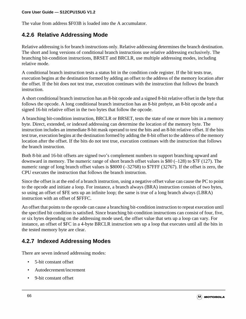
Core User Guide — S12CPU15UG V1.2
ination.. Theg
,n afternch
e thatd a
ory
e bitsemorylows
and). Theo, the
to pointbytes,)
n untilfive,y. Forbits in
The value from address $F03B is loaded into the A accumulator.
4.2.6 Relative Addressing Mode
Relative addressing is for branch instructions only. Relative addressing determines the branch destThe short and long versions of conditional branch instructions use relative addressing exclusivelybranching bit-condition instructions, BRSET and BRCLR, use multiple addressing modes, includinrelative mode.
A conditional branch instruction tests a status bit in the condition code register. If the bit tests trueexecution begins at the destination formed by adding an offset to the address of the memory locatiothe offset. If the bit does not test true, execution continues with the instruction that follows the brainstruction.
A short conditional branch instruction has an 8-bit opcode and a signed 8-bit relative offset in the bytfollows the opcode. A long conditional branch instruction has an 8-bit prebyte, an 8-bit opcode ansigned 16-bit relative offset in the two bytes that follow the opcode.
A branching bit-condition instruction, BRCLR or BRSET, tests the state of one or more bits in a membyte. Direct, extended, or indexed addressing can determine the location of the memory byte. Theinstruction includes an immediate 8-bit mask operand to test the bits and an 8-bit relative offset. If thtest true, execution begins at the destination formed by adding the 8-bit offset to the address of the mlocation after the offset. If the bits do not test true, execution continues with the instruction that folthe branch instruction.
Both 8-bit and 16-bit offsets are signed two’s complement numbers to support branching upward downward in memory. The numeric range of short branch offset values is $80 (–128) to $7F (127numeric range of long branch offset values is $8000 (–32768) to $7FFF (32767). If the offset is zerCPU executes the instruction that follows the branch instruction.
Since the offset is at the end of a branch instruction, using a negative offset value can cause the PCto the opcode and initiate a loop. For instance, a branch always (BRA) instruction consists of two so using an offset of $FE sets up an infinite loop; the same is true of a long branch always (LBRAinstruction with an offset of $FFFC.
An offset that points to the opcode can cause a branching bit-condition instruction to repeat executiothe specified bit condition is satisfied. Since branching bit-condition instructions can consist of four,or six bytes depending on the addressing mode used, the offset value that sets up a loop can varinstance, an offset of $FC in a 4-byte BRCLR instruction sets up a loop that executes until all the the tested memory byte are clear.
4.2.7 Indexed Addressing Modes
There are seven indexed addressing modes:
• 5-bit constant offset
• Autodecrement/increment
• 9-bit constant offset
66
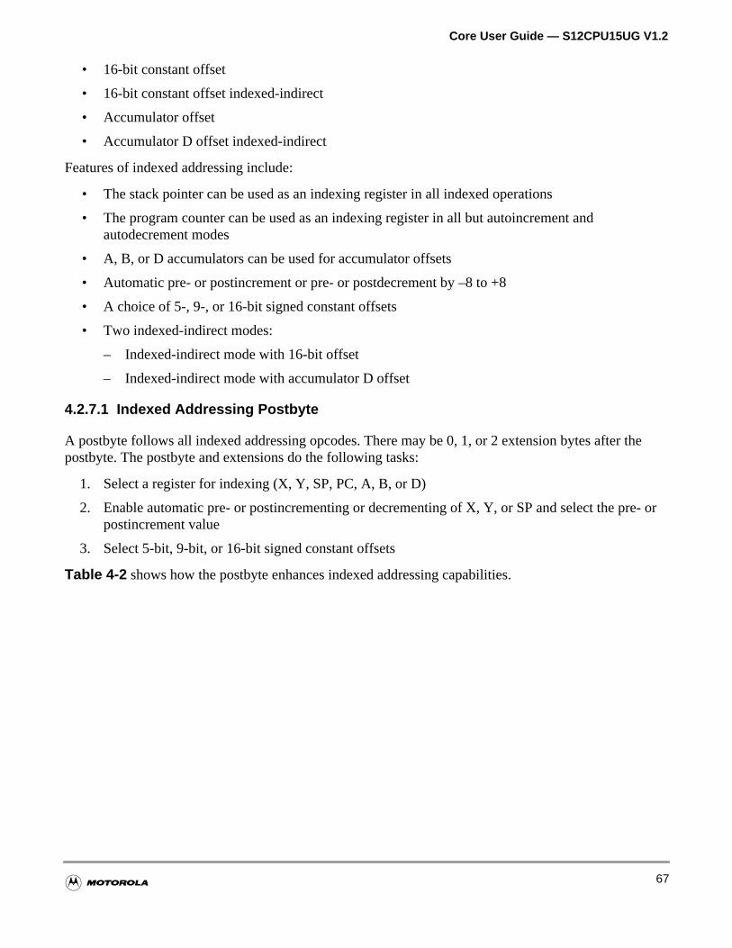
Core User Guide — S12CPU15UG V1.2
the
re- or
• 16-bit constant offset
• 16-bit constant offset indexed-indirect
• Accumulator offset
• Accumulator D offset indexed-indirect
Features of indexed addressing include:
• The stack pointer can be used as an indexing register in all indexed operations
• The program counter can be used as an indexing register in all but autoincrement andautodecrement modes
• A, B, or D accumulators can be used for accumulator offsets
• Automatic pre- or postincrement or pre- or postdecrement by –8 to +8
• A choice of 5-, 9-, or 16-bit signed constant offsets
• Two indexed-indirect modes:
– Indexed-indirect mode with 16-bit offset
– Indexed-indirect mode with accumulator D offset
4.2.7.1 Indexed Addressing Postbyte
A postbyte follows all indexed addressing opcodes. There may be 0, 1, or 2 extension bytes afterpostbyte. The postbyte and extensions do the following tasks:
1. Select a register for indexing (X, Y, SP, PC, A, B, or D)
2. Enable automatic pre- or postincrementing or decrementing of X, Y, or SP and select the ppostincrement value
3. Select 5-bit, 9-bit, or 16-bit signed constant offsets
Table 4-2 shows how the postbyte enhances indexed addressing capabilities.
67
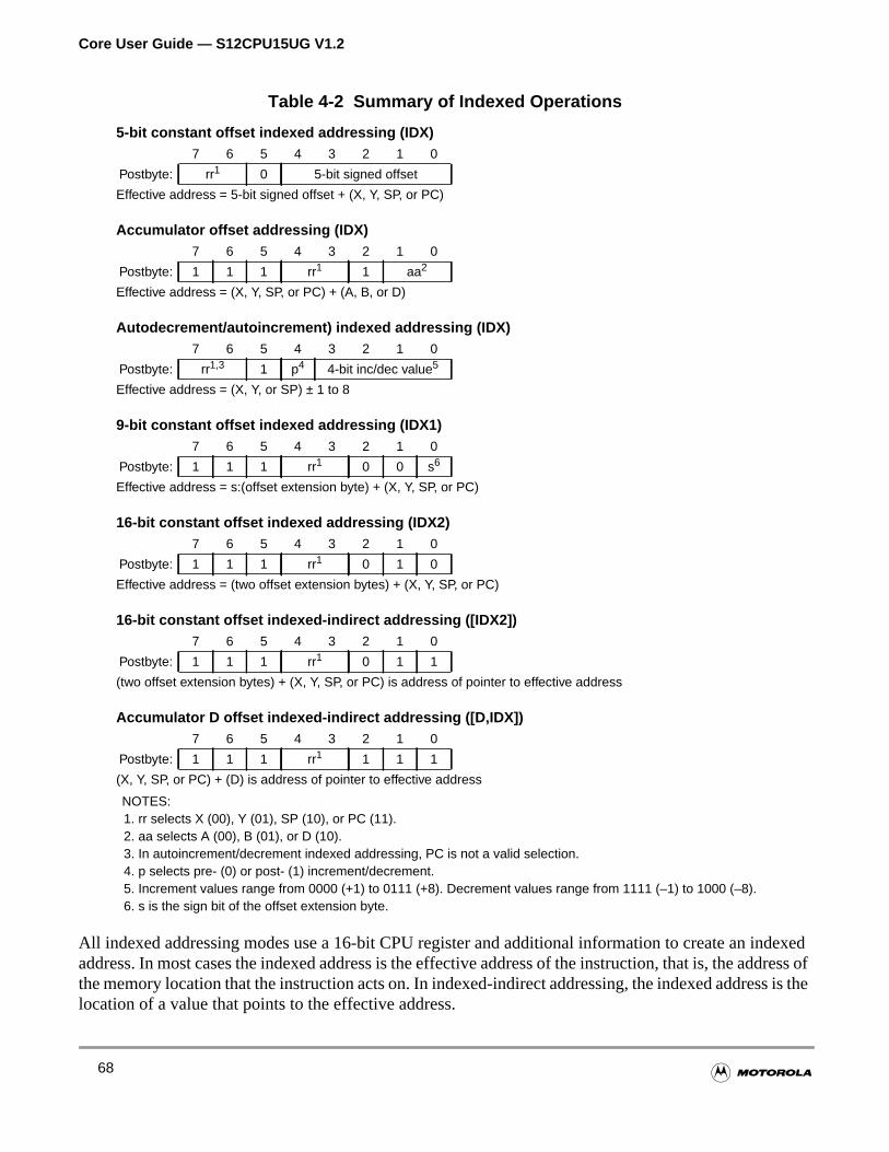
Core User Guide — S12CPU15UG V1.2
dexeddress ofs is the
All indexed addressing modes use a 16-bit CPU register and additional information to create an inaddress. In most cases the indexed address is the effective address of the instruction, that is, the adthe memory location that the instruction acts on. In indexed-indirect addressing, the indexed addreslocation of a value that points to the effective address.
Table 4-2 Summary of Indexed Operations
5-bit constant offset indexed addressing (IDX)7 6 5 4 3 2 1 0
Postbyte: rr1
NOTES:1. rr selects X (00), Y (01), SP (10), or PC (11).
0 5-bit signed offset
Effective address = 5-bit signed offset + (X, Y, SP, or PC)
Accumulator offset addressing (IDX)7 6 5 4 3 2 1 0
Postbyte: 1 1 1 rr1 1 aa2
2. aa selects A (00), B (01), or D (10).
Effective address = (X, Y, SP, or PC) + (A, B, or D)
Autodecrement/autoincrement) indexed addressing (IDX)7 6 5 4 3 2 1 0
Postbyte: rr1,3
3. In autoincrement/decrement indexed addressing, PC is not a valid selection.
1 p4
4. p selects pre- (0) or post- (1) increment/decrement.
4-bit inc/dec value5
5. Increment values range from 0000 (+1) to 0111 (+8). Decrement values range from 1111 (–1) to 1000 (–8).
Effective address = (X, Y, or SP) ± 1 to 8
9-bit constant offset indexed addressing (IDX1)7 6 5 4 3 2 1 0
Postbyte: 1 1 1 rr1 0 0 s6
6. s is the sign bit of the offset extension byte.
Effective address = s:(offset extension byte) + (X, Y, SP, or PC)
16-bit constant offset indexed addressing (IDX2)7 6 5 4 3 2 1 0
Postbyte: 1 1 1 rr1 0 1 0
Effective address = (two offset extension bytes) + (X, Y, SP, or PC)
16-bit constant offset indexed-indirect addressing ([IDX2])7 6 5 4 3 2 1 0
Postbyte: 1 1 1 rr1 0 1 1
(two offset extension bytes) + (X, Y, SP, or PC) is address of pointer to effective address
Accumulator D offset indexed-indirect addressing ([D,IDX])7 6 5 4 3 2 1 0
Postbyte: 1 1 1 rr1 1 1 1
(X, Y, SP, or PC) + (D) is address of pointer to effective address
68
Core User Guide — S12CPU15UG V1.2
e to thesigneded
on byteign bit
ytes to6-bitare both
PC offsets are calculated from the location immediately following the current instruction.
This example moves a byte of data from $2000 to $1007.
4.2.7.2 5-Bit Constant Offset Indexed Addressing
This addressing mode calculates the effective address by adding a 5-bit signed offset in the postbytindexing register (X, Y, SP, or PC). The value in the indexing register does not change. The 5-bit offset gives a range of–16 through +15 from the value in the indexing register. The majority of indexinstructions use offsets that fit in the 5-bit offset range.
For these examples, assume X contains $1000 and Y contains $2000:
The value at address $1000 is loaded into A.
The value in B is stored at address $2000 – $8, or $1FF8.
4.2.7.3 9-Bit Constant Offset Indexed Addressing
This addressing mode calculates the effective address by adding a 9-bit signed offset in an extensito the indexing register (X, Y, SP, or PC). The value in the indexing register does not change. The sof the offset is in the postbyte. The 9-bit offset gives a range of–256 through +255 from the value in theindexing register.
For these examples assume X contains $1000 and Y contains $2000:
The value at address $10FF is loaded into A.
The value at address $2000 – $14, or $1FEC, is loaded into B.
4.2.7.4 16-Bit Constant Offset Indexed Addressing
This addressing mode calculates the effective address by adding a 16-bit offset in two extension bthe indexing register (X, Y, SP, or PC). The value in the indexing register does not change. The 1offset allows access to any address in the 64K byte address space. The address bus and the offset
1000 18 09 C2 20 00 MOVB $2000 2,PC
1005 A7 NOP
LDAA 0,X
STAB –8,Y
LDAA $FF,X
LDAB –20,Y
69
Core User Guide — S12CPU15UG V1.2
ay be
ffset ins not
d
ddress
d –1 oralue.
lace.lace.
itional
y one:
uctionointer:
ction
16 bits, so it does not matter whether the offset is considered to be signed or unsigned ($FFFF mthought of as +65,535 or as–1).
4.2.7.5 16-Bit Constant Indexed-Indirect Addressing
This addressing mode calculates the address of a pointer to the effective address. It adds a 16-bit otwo extension bytes to the indexing register (X, Y, SP, or PC). The value in the indexing register doechange. The square brackets distinguish this addressing mode from 16-bit constant offset indexeaddressng.
For this example, assume X contains $1000 and the value at address $100A is $2000:
The value 10 is added to the value in X to form the address $100A. The CPU fetches the effective apointer, $2000, from address $100A and loads the value at address $2000 into A.
4.2.7.6 Autodecrement/Autoincrement Indexed Addressing
This addressing mode calculates the effective address by adding an integer value between –8 anbetween 1 and 8 to the indexing register (X, Y, or SP). The indexing register retains its changed v
NOTE: Autodecrementing and autoincrementing do not apply to the program counter.
When predecremented or preincremented, the indexing register changes before indexing takes pWhen postdecremented or postincremented, the indexing register changes after indexing takes p
This addressing mode adjusts the indexing value without increasing execution time by using an addinstruction.
In this example, the instruction compares X with the value that X points to and then increments X b
The next two examples are equivalent to common push instructions. In the first example, the instrpredecrements the stack pointer by one and then stores A to the address contained in the stack p
The next two examples are equivalent to common pull instructions. In the first example, the instruloads X from the address in the stack pointer and then postincrements the stack pointer by two:
LDAA [10,X]
CPX 1,X+
STAA 1,–SP ;equivalent to PSHA
STX 2,–SP ;equivalent to PSHX
LDX 2,SP+ ;equivalent to PULX
LDAA 1,SP+ ;equivalent to PULA
70
Core User Guide — S12CPU15UG V1.2
ith thisentrypointeremory:
tivesion of
r to and. The
nged11.
to the. The
e timelues
ddresshe
ation
The next example demonstrates how to work with data structures larger than bytes and words. Winstruction in a program loop, it is possible to move words of data from a list having one word per into a second table that has four bytes per table element. The instruction postincrements the sourceafter reading the data from memory and preincrements the destination pointer before accessing m
Using a predecrement/increment version of LEAS, LEAX, or LEAY when SP, X, or Y is the respecindexing register changes the value in the indexing register. Using a postdecrement/increment verLEAS, LEAX, LEAY when SP, X, or Y is the respective indexing register has no effect.
4.2.7.7 Accumulator Offset Indexed Addressing
This addressing mode calculates the effective address by adding the value in the indexing registeunsigned offset value in one of the accumulators. The value in the indexing register is not changeindexing register can be X, Y, SP, or PC, and the accumulator can be A, B, or D.
Example:
This instruction adds B to X to form the address from which A will be loaded. B and X are not chaby this instruction. This example is similar to the following two-instruction combination in an M68HC
4.2.7.8 Accumulator D Indexed-Indirect Addressing
This addressing mode calculates address of a pointer to the effective address. It adds the value in Dvalue in the indexing register (X, Y, SP, or PC) The value in the indexing register does not changesquare brackets distinguish this addressing mode from D accumulator offset indexing.
In this example, accumulator D indexed-indirect addressing is used in a computed GOTO:
The values beginning at GO1 are addresses of potential destinations of the jump instruction. At ththe JMP [D,PC] instruction is executed, PC points to the address GO1, and D holds one of the va$0000, $0002, or $0004, determined by the program some time before the JMP.
Assume that the value in D is $0002. The JMP instruction adds the values in D and PC to form the aof GO2. Next the CPU reads the address PLACE2 from memory at GO2 and jumps to PLACE2. Tlocations of PLACE1 through PLACE3 were known at the time of program assembly but the destinof the JMP depends upon the value in D computed during program execution.
4.2.8 Instructions Using Multiple Modes
Several instructions use more than one addressing mode in the course of execution.
MOVW 2,X+,4,+Y
LDAA B,X
JMP [D,PC]
GO1 DC.W PLACE1
GO2 DC.W PLACE2
GO3 DC.W PLACE3
71
Core User Guide — S12CPU15UG V1.2
dressingended,
dethe
ans the
maskminest offset
4.2.8.1 Move Instructions
Move instructions can use one addressing mode to access the source of the move and another admode to access the destination. There are move variations for most combinations of immediate, extand indexed addressing modes.
The only combinations of addressing modes that are not allowed are those with an immediate modestination; the operand of an immediate instruction is data, not an address. For indexed moves, indexing register can be X, Y, SP, or PC.
Move instructions do not have indirect modes, or 9-bit or 16-bit offset modes.
4.2.8.2 Bit Manipulation Instructions
Bit manipulation instructions use a combination of two or three addressing modes.
A BCLR or BSET instruction has an 8-bit mask to clear or set bits in a memory byte. The mask is immediate value supplied with the instruction. Direct, extended, or indexed addressing determinelocation of the memory byte.
A BRCLR or BRSET instruction has an 8-bit mask to test the states of bits in a memory byte. Theis an immediate value supplied with the instruction. Direct, extended, or indexed addressing deterthe location of the memory byte. Relative addressing determines the branch address. A signed 8-bimust be supplied with the instruction.
72
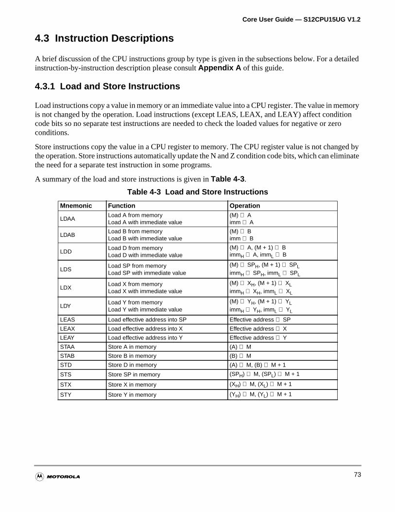
Core User Guide — S12CPU15UG V1.2
tailed
moryonero
ed byinate
4.3 Instruction Descriptions
A brief discussion of the CPU instructions group by type is given in the subsections below. For a deinstruction-by-instruction description please consultAppendix A of this guide.
4.3.1 Load and Store Instructions
Load instructions copy a value in memory or an immediate value into a CPU register. The value in meis not changed by the operation. Load instructions (except LEAS, LEAX, and LEAY) affect conditicode bits so no separate test instructions are needed to check the loaded values for negative or zconditions.
Store instructions copy the value in a CPU register to memory. The CPU register value is not changthe operation. Store instructions automatically update the N and Z condition code bits, which can elimthe need for a separate test instruction in some programs.
A summary of the load and store instructions is given inTable 4-3 .
Table 4-3 Load and Store Instructions
Mnemonic Function Operation
LDAALoad A from memoryLoad A with immediate value
(M) ⇒ Aimm ⇒ A
LDABLoad B from memoryLoad B with immediate value
(M) ⇒ Bimm ⇒ B
LDDLoad D from memoryLoad D with immediate value
(M) ⇒ A, (M + 1) ⇒ BimmH ⇒ A, immL ⇒ B
LDSLoad SP from memoryLoad SP with immediate value
(M) ⇒ SPH, (M + 1) ⇒ SPLimmH ⇒ SPH, immL ⇒ SPL
LDXLoad X from memoryLoad X with immediate value
(M) ⇒ XH, (M + 1) ⇒ XLimmH ⇒ XH, immL ⇒ XL
LDYLoad Y from memoryLoad Y with immediate value
(M) ⇒ YH, (M + 1) ⇒ YLimmH ⇒ YH, immL ⇒ YL
LEAS Load effective address into SP Effective address ⇒ SP
LEAX Load effective address into X Effective address ⇒ X
LEAY Load effective address into Y Effective address ⇒ Y
STAA Store A in memory (A) ⇒ M
STAB Store B in memory (B) ⇒ M
STD Store D in memory (A) ⇒ M, (B) ⇒ M + 1
STS Store SP in memory (SPH) ⇒ M, (SPL) ⇒ M + 1
STX Store X in memory (XH) ⇒ M, (XL) ⇒ M + 1
STY Store Y in memory (YH) ⇒ M, (YL) ⇒ M + 1
73
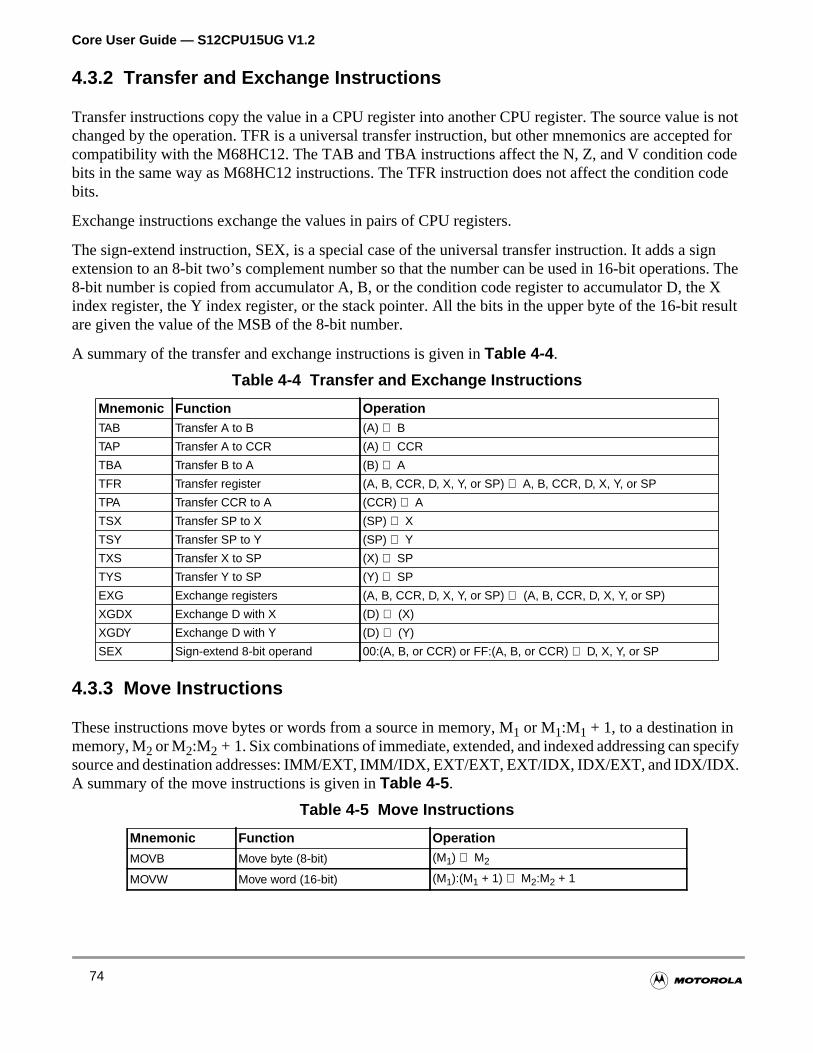
Core User Guide — S12CPU15UG V1.2
is notted forodecode
igns. The Xresult
ecify.
4.3.2 Transfer and Exchange Instructions
Transfer instructions copy the value in a CPU register into another CPU register. The source valuechanged by the operation. TFR is a universal transfer instruction, but other mnemonics are accepcompatibility with the M68HC12. The TAB and TBA instructions affect the N, Z, and V condition cbits in the same way as M68HC12 instructions. The TFR instruction does not affect the condition bits.
Exchange instructions exchange the values in pairs of CPU registers.
The sign-extend instruction, SEX, is a special case of the universal transfer instruction. It adds a sextension to an 8-bit two’s complement number so that the number can be used in 16-bit operation8-bit number is copied from accumulator A, B, or the condition code register to accumulator D, theindex register, the Y index register, or the stack pointer. All the bits in the upper byte of the 16-bit are given the value of the MSB of the 8-bit number.
A summary of the transfer and exchange instructions is given inTable 4-4 .
4.3.3 Move Instructions
These instructions move bytes or words from a source in memory, M1 or M1:M1 + 1, to a destination inmemory, M2 or M2:M2 + 1. Six combinations of immediate, extended, and indexed addressing can spsource and destination addresses: IMM/EXT, IMM/IDX, EXT/EXT, EXT/IDX, IDX/EXT, and IDX/IDXA summary of the move instructions is given inTable 4-5 .
Table 4-4 Transfer and Exchange Instructions
Mnemonic Function OperationTAB Transfer A to B (A) ⇒ B
TAP Transfer A to CCR (A) ⇒ CCR
TBA Transfer B to A (B) ⇒ A
TFR Transfer register (A, B, CCR, D, X, Y, or SP) ⇒ A, B, CCR, D, X, Y, or SP
TPA Transfer CCR to A (CCR) ⇒ A
TSX Transfer SP to X (SP) ⇒ X
TSY Transfer SP to Y (SP) ⇒ Y
TXS Transfer X to SP (X) ⇒ SP
TYS Transfer Y to SP (Y) ⇒ SP
EXG Exchange registers (A, B, CCR, D, X, Y, or SP) ⇔ (A, B, CCR, D, X, Y, or SP)
XGDX Exchange D with X (D) ⇔ (X)
XGDY Exchange D with Y (D) ⇔ (Y)
SEX Sign-extend 8-bit operand 00:(A, B, or CCR) or FF:(A, B, or CCR) ⇒ D, X, Y, or SP
Table 4-5 Move Instructions
Mnemonic Function Operation
MOVB Move byte (8-bit) (M1) ⇒ M2
MOVW Move word (16-bit) (M1):(M1 + 1) ⇒ M2:M2 + 1
74
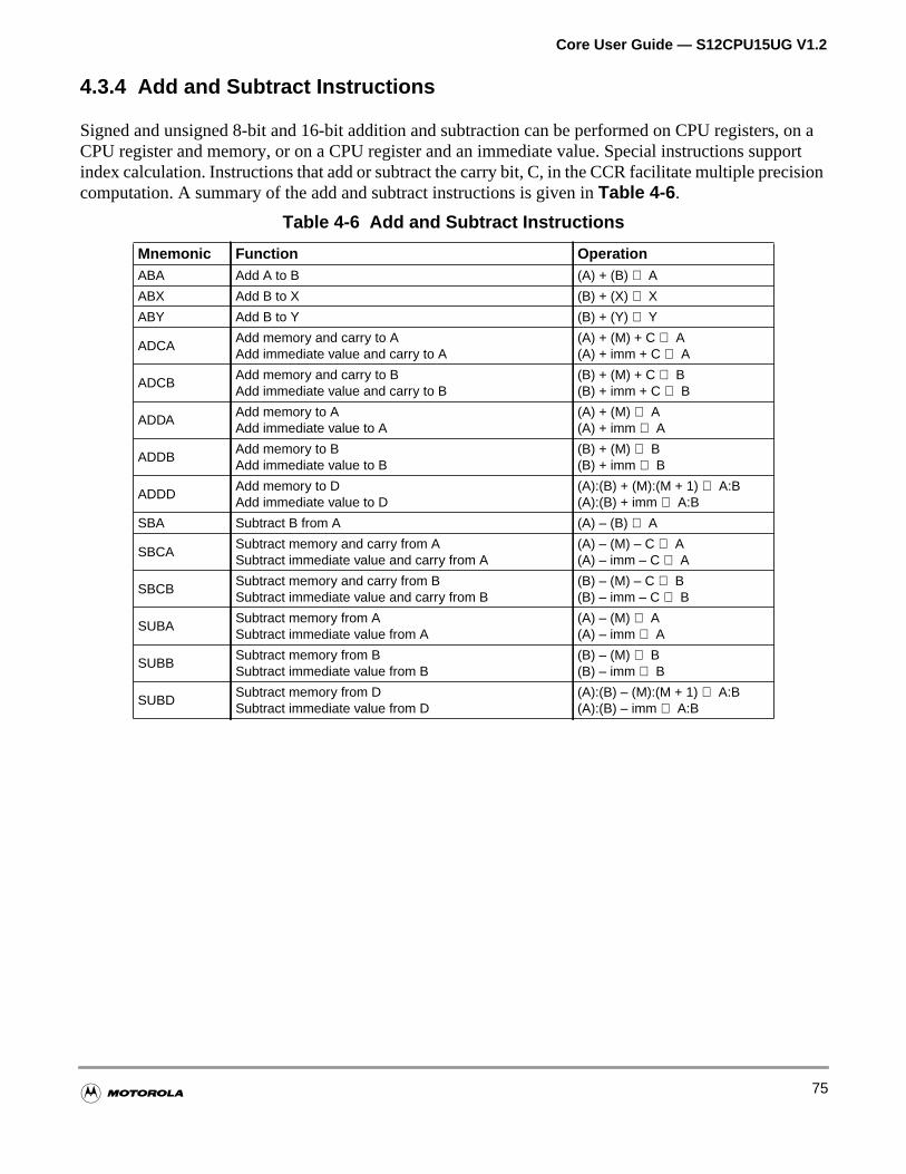
Core User Guide — S12CPU15UG V1.2
, on aport
ision
4.3.4 Add and Subtract Instructions
Signed and unsigned 8-bit and 16-bit addition and subtraction can be performed on CPU registersCPU register and memory, or on a CPU register and an immediate value. Special instructions supindex calculation. Instructions that add or subtract the carry bit, C, in the CCR facilitate multiple preccomputation. A summary of the add and subtract instructions is given inTable 4-6 .
Table 4-6 Add and Subtract Instructions
Mnemonic Function OperationABA Add A to B (A) + (B) ⇒ A
ABX Add B to X (B) + (X) ⇒ X
ABY Add B to Y (B) + (Y) ⇒ Y
ADCAAdd memory and carry to AAdd immediate value and carry to A
(A) + (M) + C ⇒ A(A) + imm + C ⇒ A
ADCBAdd memory and carry to BAdd immediate value and carry to B
(B) + (M) + C ⇒ B(B) + imm + C ⇒ B
ADDAAdd memory to AAdd immediate value to A
(A) + (M) ⇒ A(A) + imm ⇒ A
ADDBAdd memory to BAdd immediate value to B
(B) + (M) ⇒ B(B) + imm ⇒ B
ADDDAdd memory to DAdd immediate value to D
(A):(B) + (M):(M + 1) ⇒ A:B(A):(B) + imm ⇒ A:B
SBA Subtract B from A (A) – (B) ⇒ A
SBCASubtract memory and carry from ASubtract immediate value and carry from A
(A) – (M) – C ⇒ A(A) – imm – C ⇒ A
SBCBSubtract memory and carry from BSubtract immediate value and carry from B
(B) – (M) – C ⇒ B(B) – imm – C ⇒ B
SUBASubtract memory from ASubtract immediate value from A
(A) – (M) ⇒ A(A) – imm ⇒ A
SUBBSubtract memory from BSubtract immediate value from B
(B) – (M) ⇒ B(B) – imm ⇒ B
SUBDSubtract memory from DSubtract immediate value from D
(A):(B) – (M):(M + 1) ⇒ A:B(A):(B) – imm ⇒ A:B
75
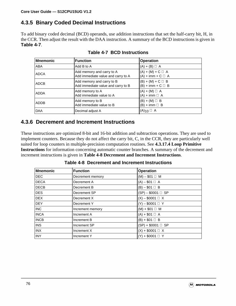
Core User Guide — S12CPU15UG V1.2
H, inn in
ed towell
and
4.3.5 Binary Coded Decimal Instructions
To add binary coded decimal (BCD) operands, use addition instructions that set the half-carry bit,the CCR. Then adjust the result with the DAA instruction. A summary of the BCD instructions is giveTable 4-7 .
4.3.6 Decrement and Increment Instructions
These instructions are optimized 8-bit and 16-bit addition and subtraction operations. They are usimplement counters. Because they do not affect the carry bit, C, in the CCR, they are particularly suited for loop counters in multiple-precision computation routines. See4.3.17.4 Loop PrimitiveInstructions for information concerning automatic counter branches. A summary of the decrementincrement instructions is given inTable 4-8 Decrement and Increment Instructions.
Table 4-7 BCD Instructions
Mnemonic Function OperationABA Add B to A (A) + (B) ⇒ A
ADCAAdd memory and carry to AAdd immediate value and carry to A
(A) + (M) + C ⇒ A(A) + imm + C ⇒ A
ADCBAdd memory and carry to BAdd immediate value and carry to B
(B) + (M) + C ⇒ B(B) + imm + C ⇒ B
ADDAAdd memory to AAdd immediate value to A
(A) + (M) ⇒ A(A) + imm ⇒ A
ADDBAdd memory to BAdd immediate value to B
(B) + (M) ⇒ B(B) + imm ⇒ B
DAA Decimal adjust A (A)10 ⇒ A
Table 4-8 Decrement and Increment Instructions
Mnemonic Function OperationDEC Decrement memory (M) – $01 ⇒ M
DECA Decrement A (A) – $01 ⇒ A
DECB Decrement B (B) – $01 ⇒ B
DES Decrement SP (SP) – $0001 ⇒ SP
DEX Decrement X (X) – $0001 ⇒ X
DEY Decrement Y (Y) – $0001 ⇒ Y
INC Increment memory (M) + $01 ⇒ M
INCA Increment A (A) + $01 ⇒ A
INCB Increment B (B) + $01 ⇒ B
INS Increment SP (SP) + $0001 ⇒ SP
INX Increment X (X) + $0001 ⇒ X
INY Increment Y (Y) + $0001 ⇒ Y
76
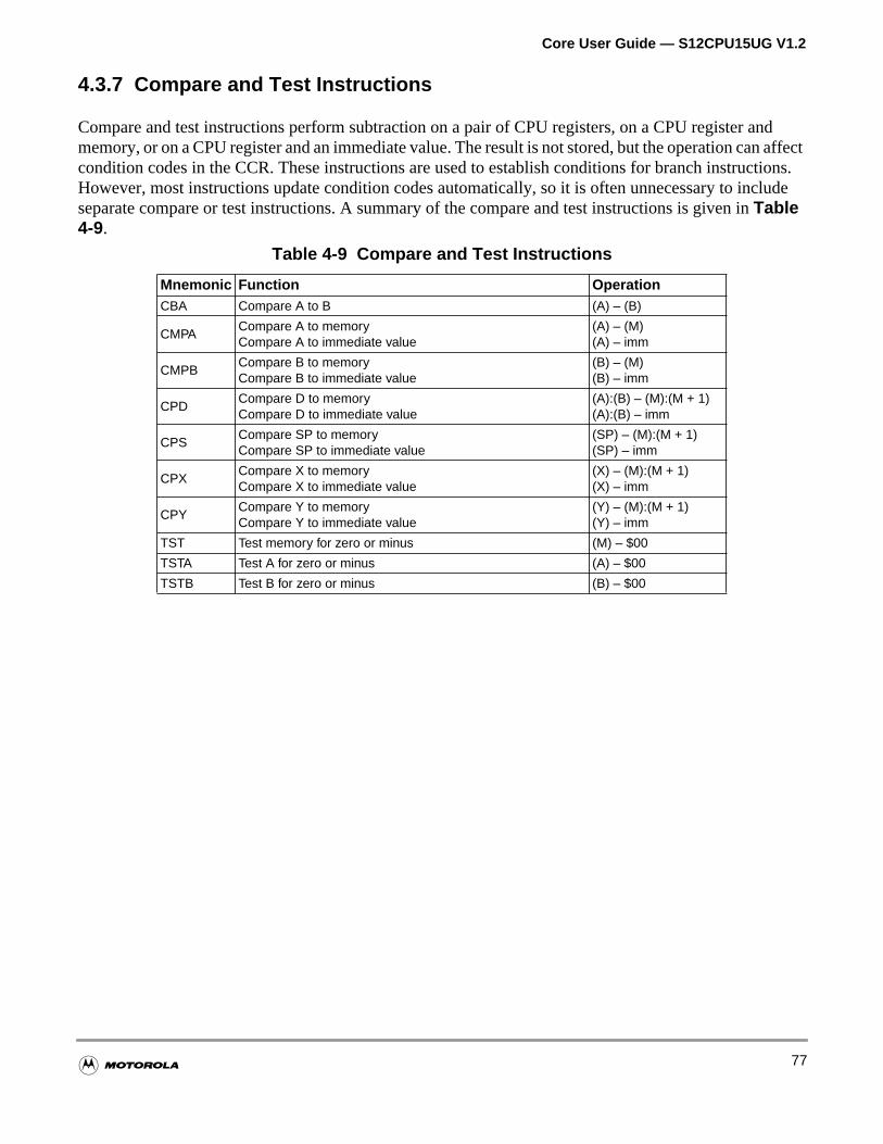
Core User Guide — S12CPU15UG V1.2
ndaffect
tions.lude
4.3.7 Compare and Test Instructions
Compare and test instructions perform subtraction on a pair of CPU registers, on a CPU register amemory, or on a CPU register and an immediate value. The result is not stored, but the operation cancondition codes in the CCR. These instructions are used to establish conditions for branch instrucHowever, most instructions update condition codes automatically, so it is often unnecessary to incseparate compare or test instructions. A summary of the compare and test instructions is given inTable4-9.
Table 4-9 Compare and Test Instructions
Mnemonic Function OperationCBA Compare A to B (A) – (B)
CMPACompare A to memoryCompare A to immediate value
(A) – (M)(A) – imm
CMPBCompare B to memoryCompare B to immediate value
(B) – (M)(B) – imm
CPDCompare D to memoryCompare D to immediate value
(A):(B) – (M):(M + 1)(A):(B) – imm
CPSCompare SP to memoryCompare SP to immediate value
(SP) – (M):(M + 1)(SP) – imm
CPXCompare X to memoryCompare X to immediate value
(X) – (M):(M + 1)(X) – imm
CPYCompare Y to memoryCompare Y to immediate value
(Y) – (M):(M + 1)(Y) – imm
TST Test memory for zero or minus (M) – $00
TSTA Test A for zero or minus (A) – $00
TSTB Test B for zero or minus (B) – $00
77
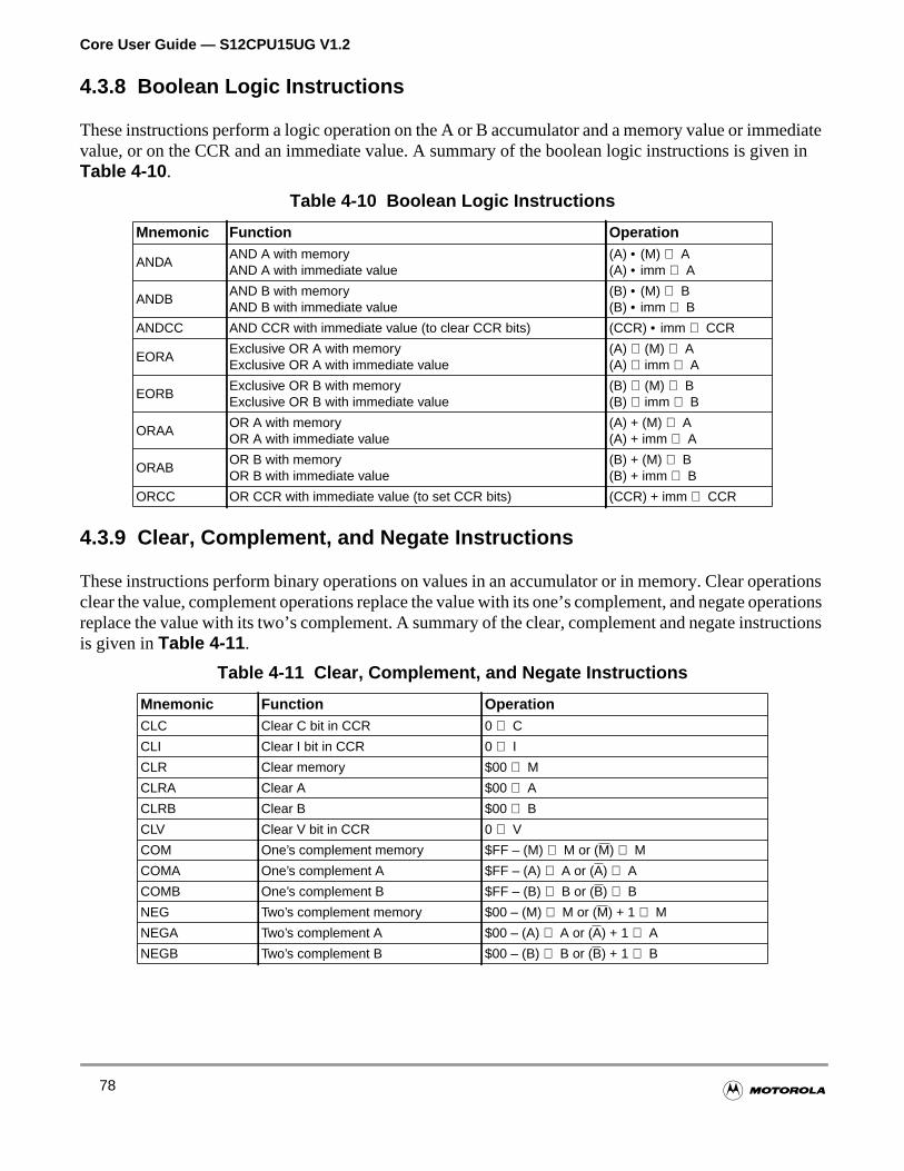
Core User Guide — S12CPU15UG V1.2
diaten in
ationsrations
ctions
4.3.8 Boolean Logic Instructions
These instructions perform a logic operation on the A or B accumulator and a memory value or immevalue, or on the CCR and an immediate value. A summary of the boolean logic instructions is giveTable 4-10 .
4.3.9 Clear, Complement, and Negate Instructions
These instructions perform binary operations on values in an accumulator or in memory. Clear operclear the value, complement operations replace the value with its one’s complement, and negate opereplace the value with its two’s complement. A summary of the clear, complement and negate instruis given inTable 4-11 .
Table 4-10 Boolean Logic Instructions
Mnemonic Function Operation
ANDAAND A with memoryAND A with immediate value
(A) • (M) ⇒ A(A) • imm ⇒ A
ANDBAND B with memoryAND B with immediate value
(B) • (M) ⇒ B(B) • imm ⇒ B
ANDCC AND CCR with immediate value (to clear CCR bits) (CCR) • imm ⇒ CCR
EORAExclusive OR A with memoryExclusive OR A with immediate value
(A) ⊕ (M) ⇒ A(A) ⊕ imm ⇒ A
EORBExclusive OR B with memoryExclusive OR B with immediate value
(B) ⊕ (M) ⇒ B(B) ⊕ imm ⇒ B
ORAAOR A with memoryOR A with immediate value
(A) + (M) ⇒ A(A) + imm ⇒ A
ORABOR B with memoryOR B with immediate value
(B) + (M) ⇒ B(B) + imm ⇒ B
ORCC OR CCR with immediate value (to set CCR bits) (CCR) + imm ⇒ CCR
Table 4-11 Clear, Complement, and Negate Instructions
Mnemonic Function OperationCLC Clear C bit in CCR 0 ⇒ C
CLI Clear I bit in CCR 0 ⇒ I
CLR Clear memory $00 ⇒ M
CLRA Clear A $00 ⇒ A
CLRB Clear B $00 ⇒ B
CLV Clear V bit in CCR 0 ⇒ V
COM One’s complement memory $FF – (M) ⇒ M or (M) ⇒ M
COMA One’s complement A $FF – (A) ⇒ A or (A) ⇒ A
COMB One’s complement B $FF – (B) ⇒ B or (B) ⇒ B
NEG Two’s complement memory $00 – (M) ⇒ M or (M) + 1 ⇒ M
NEGA Two’s complement A $00 – (A) ⇒ A or (A) + 1 ⇒ A
NEGB Two’s complement B $00 – (B) ⇒ B or (B) + 1 ⇒ B
78
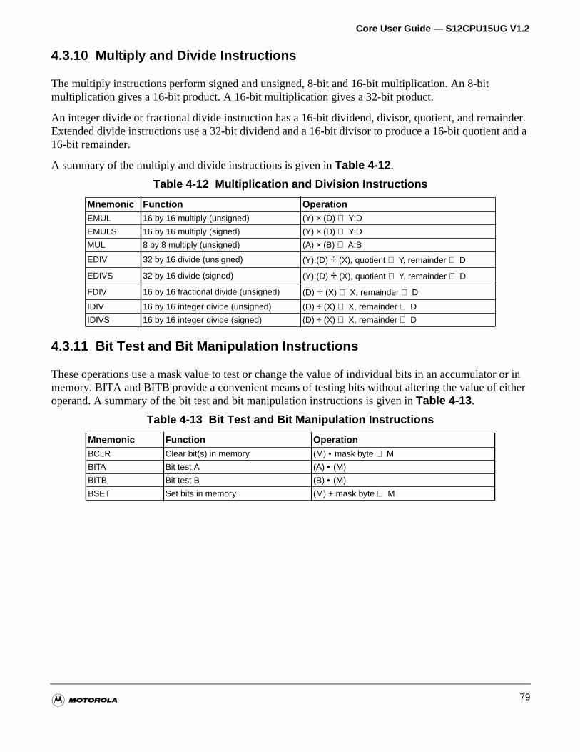
Core User Guide — S12CPU15UG V1.2
der.and a
r or inither
4.3.10 Multiply and Divide Instructions
The multiply instructions perform signed and unsigned, 8-bit and 16-bit multiplication. An 8-bitmultiplication gives a 16-bit product. A 16-bit multiplication gives a 32-bit product.
An integer divide or fractional divide instruction has a 16-bit dividend, divisor, quotient, and remainExtended divide instructions use a 32-bit dividend and a 16-bit divisor to produce a 16-bit quotient16-bit remainder.
A summary of the multiply and divide instructions is given inTable 4-12 .
4.3.11 Bit Test and Bit Manipulation Instructions
These operations use a mask value to test or change the value of individual bits in an accumulatomemory. BITA and BITB provide a convenient means of testing bits without altering the value of eoperand. A summary of the bit test and bit manipulation instructions is given inTable 4-13 .
Table 4-12 Multiplication and Division Instructions
Mnemonic Function OperationEMUL 16 by 16 multiply (unsigned) (Y) × (D) ⇒ Y:D
EMULS 16 by 16 multiply (signed) (Y) × (D) ⇒ Y:D
MUL 8 by 8 multiply (unsigned) (A) × (B) ⇒ A:B
EDIV 32 by 16 divide (unsigned) (Y):(D) ÷ (X), quotient ⇒ Y, remainder ⇒ D
EDIVS 32 by 16 divide (signed) (Y):(D) ÷ (X), quotient ⇒ Y, remainder ⇒ D
FDIV 16 by 16 fractional divide (unsigned) (D) ÷ (X) ⇒ X, remainder ⇒ D
IDIV 16 by 16 integer divide (unsigned) (D) ÷ (X) ⇒ X, remainder ⇒ D
IDIVS 16 by 16 integer divide (signed) (D) ÷ (X) ⇒ X, remainder ⇒ D
Table 4-13 Bit Test and Bit Manipulation Instructions
Mnemonic Function OperationBCLR Clear bit(s) in memory (M) • mask byte ⇒ M
BITA Bit test A (A) • (M)
BITB Bit test B (B) • (M)
BSET Set bits in memory (M) + mask byte ⇒ M
79
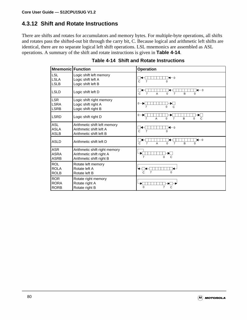
Core User Guide — S12CPU15UG V1.2
shiftsifts areL
4.3.12 Shift and Rotate Instructions
There are shifts and rotates for accumulators and memory bytes. For multiple-byte operations, alland rotates pass the shifted-out bit through the carry bit, C. Because logical and arithmetic left shidentical, there are no separate logical left shift operations. LSL mnemonics are assembled as ASoperations. A summary of the shift and rotate instructions is given inTable 4-14 .
Table 4-14 Shift and Rotate Instructions
Mnemonic Function OperationLSLLSLALSLB
Logic shift left memoryLogic shift left ALogic shift left B
LSLD Logic shift left D
LSRLSRALSRB
Logic shift right memoryLogic shift right ALogic shift right B
LSRD Logic shift right D
ASLASLAASLB
Arithmetic shift left memoryArithmetic shift left AArithmetic shift left B
ASLD Arithmetic shift left D
ASRASRAASRB
Arithmetic shift right memoryArithmetic shift right AArithmetic shift right B
ROLROLAROLB
Rotate left memoryRotate left ARotate left B
RORRORARORB
Rotate right memoryRotate right ARotate right B
C0
7 0
C0
7 0A B70
C0
7 0
C7 0A B700
C0
7 0
C0
7 0A B70
C7 0
C 7 0
C70
80
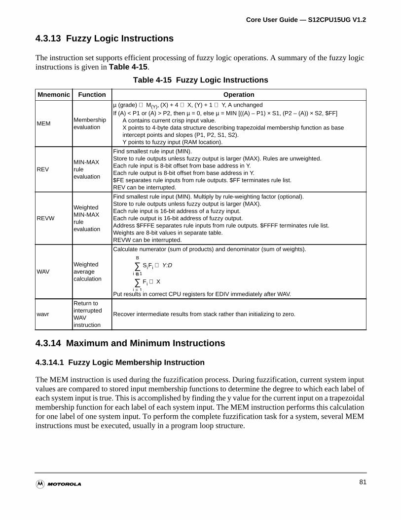
Core User Guide — S12CPU15UG V1.2
logic
putlabel ofzoidalation
EM
4.3.13 Fuzzy Logic Instructions
The instruction set supports efficient processing of fuzzy logic operations. A summary of the fuzzyinstructions is given inTable 4-15 .
4.3.14 Maximum and Minimum Instructions
4.3.14.1 Fuzzy Logic Membership Instruction
The MEM instruction is used during the fuzzification process. During fuzzification, current system invalues are compared to stored input membership functions to determine the degree to which eacheach system input is true. This is accomplished by finding the y value for the current input on a trapemembership function for each label of each system input. The MEM instruction performs this calculfor one label of one system input. To perform the complete fuzzification task for a system, several Minstructions must be executed, usually in a program loop structure.
Table 4-15 Fuzzy Logic Instructions
Mnemonic Function Operation
MEMMembershipevaluation
µ (grade) ⇒ M(Y), (X) + 4 ⇒ X, (Y) + 1 ⇒ Y, A unchangedIf (A) < P1 or (A) > P2, then µ = 0, else µ = MIN [((A) – P1) × S1, (P2 – (A)) × S2, $FF]
A contains current crisp input value.X points to 4-byte data structure describing trapezoidal membership function as baseintercept points and slopes (P1, P2, S1, S2).Y points to fuzzy input (RAM location).
REVMIN-MAXruleevaluation
Find smallest rule input (MIN).Store to rule outputs unless fuzzy output is larger (MAX). Rules are unweighted.Each rule input is 8-bit offset from base address in Y.Each rule output is 8-bit offset from base address in Y.$FE separates rule inputs from rule outputs. $FF terminates rule list.REV can be interrupted.
REVW
WeightedMIN-MAXruleevaluation
Find smallest rule input (MIN). Multiply by rule-weighting factor (optional).Store to rule outputs unless fuzzy output is larger (MAX).Each rule input is 16-bit address of a fuzzy input.Each rule output is 16-bit address of fuzzy output.Address $FFFE separates rule inputs from rule outputs. $FFFF terminates rule list.Weights are 8-bit values in separate table.REVW can be interrupted.
WAVWeightedaveragecalculation
Calculate numerator (sum of products) and denominator (sum of weights).
Put results in correct CPU registers for EDIV immediately after WAV.
wavr
Return tointerruptedWAVinstruction
Recover intermediate results from stack rather than initializing to zero.
SiFii 1=
B
∑ Y:D⇒
Fii 1=
B
∑ X⇒
81

Core User Guide — S12CPU15UG V1.2
zzye baseEVW way
. Once
ed byeffect
efined
ist of thee
uction
be used
INalue)imum
4.3.14.2 Fuzzy Logic Rule Evaluation Instructions
The REV and REVW instructions perform MIN-MAX rule evaluations that are central elements of a fulogic inference program. Fuzzy input values are processed using a list of rules from the knowledgto produce a list of fuzzy outputs. The REV instruction treats all rules as equally important. The Rinstruction allows each rule to have a separate weighting factor. REV and REVW also differ in therules are encoded into the knowledge base.
Because they require a number of cycles to execute, rule evaluation instructions can be interruptedthe interrupt has been serviced, instruction execution resumes at the point the interrupt occurred.
4.3.14.3 Fuzzy Logic Averaging Instruction
The WAV instruction calculates weighted averages. In order to be usable, the fuzzy outputs producrule evaluation must be defuzzified to produce a single output value which represents the combinedof all of the fuzzy outputs. Fuzzy outputs correspond to the labels of a system output and each is dby a membership function in the knowledge base. The CPU typically uses singletons for outputmembership functions rather than the trapezoidal shapes used for inputs. As with inputs, the x-axrepresents the range of possible values for a system output. Singleton membership functions consisx-axis position for a label of the system output. Fuzzy outputs correspond to the y-axis height of thcorresponding output membership function. The WAV instruction calculates the numerator anddenominator sums for a weighted average of the fuzzy outputs.
Because WAV requires a number of cycles to execute, it can be interrupted. The wavr pseudoinstrcauses execution to resume at the point where it was interrupted.
These instructions make comparisons between an accumulator and a memory location. They canfor linear programming operations such as Simplex-method optimization or for fuzzification.
MAX and MIN instructions use accumulator A to perform 8-bit comparisons, while EMAX and EMinstructions use accumulator D to perform 16-bit comparisons. The result (maximum or minimum vcan be stored in the accumulator or in the memory location. A summary of the minimum and maxinstructions is given inTable 4-16 .
Table 4-16 Minimum and Maximum Instructions
Mnemonic Function OperationEMIND Put smaller of two unsigned 16-bit values in D MIN [(D), (M):(M + 1)] ⇒ D
EMINM Put smaller of two unsigned 16-bit values in memory MIN [(D), (M):(M + 1)] ⇒ M:M + 1
MINA Put smaller of two unsigned 8-bit values in A MIN [(A), (M)] ⇒ A
MINM Put smaller of two unsigned 8-bit values in memory MIN [(A), (M)] ⇒ M
EMAXD Put larger of two unsigned 16-bit values in D MAX [(D), (M):(M + 1)] ⇒ D
EMAXM Put larger of two unsigned 16-bit values in memory MAX [(D), (M):(M + 1)] ⇒ M:M + 1
MAXA Put larger of two unsigned 8-bit values in A MAX [(A), (M)] ⇒ A
MAXM Put larger of two unsigned 8-bit values in memory MAX[(A), (M)] ⇒ M
82
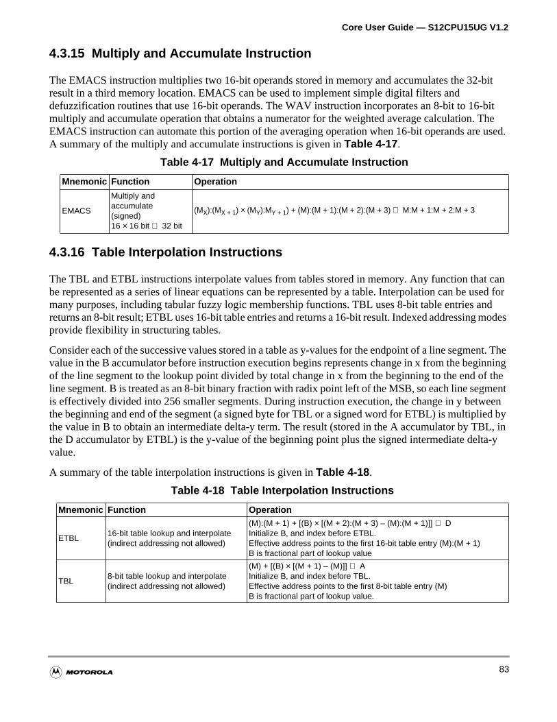
Core User Guide — S12CPU15UG V1.2
-bit
-bit Theused.
t can used forndmodes
nt. Theinningof thementeen
d byL, inta-y
4.3.15 Multiply and Accumulate Instruction
The EMACS instruction multiplies two 16-bit operands stored in memory and accumulates the 32result in a third memory location. EMACS can be used to implement simple digital filters anddefuzzification routines that use 16-bit operands. The WAV instruction incorporates an 8-bit to 16multiply and accumulate operation that obtains a numerator for the weighted average calculation.EMACS instruction can automate this portion of the averaging operation when 16-bit operands areA summary of the multiply and accumulate instructions is given inTable 4-17 .
4.3.16 Table Interpolation Instructions
The TBL and ETBL instructions interpolate values from tables stored in memory. Any function thabe represented as a series of linear equations can be represented by a table. Interpolation can bemany purposes, including tabular fuzzy logic membership functions. TBL uses 8-bit table entries areturns an 8-bit result; ETBL uses 16-bit table entries and returns a 16-bit result. Indexed addressingprovide flexibility in structuring tables.
Consider each of the successive values stored in a table as y-values for the endpoint of a line segmevalue in the B accumulator before instruction execution begins represents change in x from the begof the line segment to the lookup point divided by total change in x from the beginning to the end line segment. B is treated as an 8-bit binary fraction with radix point left of the MSB, so each line segis effectively divided into 256 smaller segments. During instruction execution, the change in y betwthe beginning and end of the segment (a signed byte for TBL or a signed word for ETBL) is multipliethe value in B to obtain an intermediate delta-y term. The result (stored in the A accumulator by TBthe D accumulator by ETBL) is the y-value of the beginning point plus the signed intermediate delvalue.
A summary of the table interpolation instructions is given inTable 4-18 .
Table 4-17 Multiply and Accumulate Instruction
Mnemonic Function Operation
EMACS
Multiply andaccumulate(signed)16 × 16 bit ⇒ 32 bit
(MX):(MX + 1) × (MY):MY + 1) + (M):(M + 1):(M + 2):(M + 3) ⇒ M:M + 1:M + 2:M + 3
Table 4-18 Table Interpolation Instructions
Mnemonic Function Operation
ETBL16-bit table lookup and interpolate(indirect addressing not allowed)
(M):(M + 1) + [(B) × [(M + 2):(M + 3) – (M):(M + 1)]] ⇒ DInitialize B, and index before ETBL.Effective address points to the first 16-bit table entry (M):(M + 1)B is fractional part of lookup value
TBL8-bit table lookup and interpolate(indirect addressing not allowed)
(M) + [(B) × [(M + 1) – (M)]] ⇒ AInitialize B, and index before TBL.Effective address points to the first 8-bit table entry (M)B is fractional part of lookup value.
83
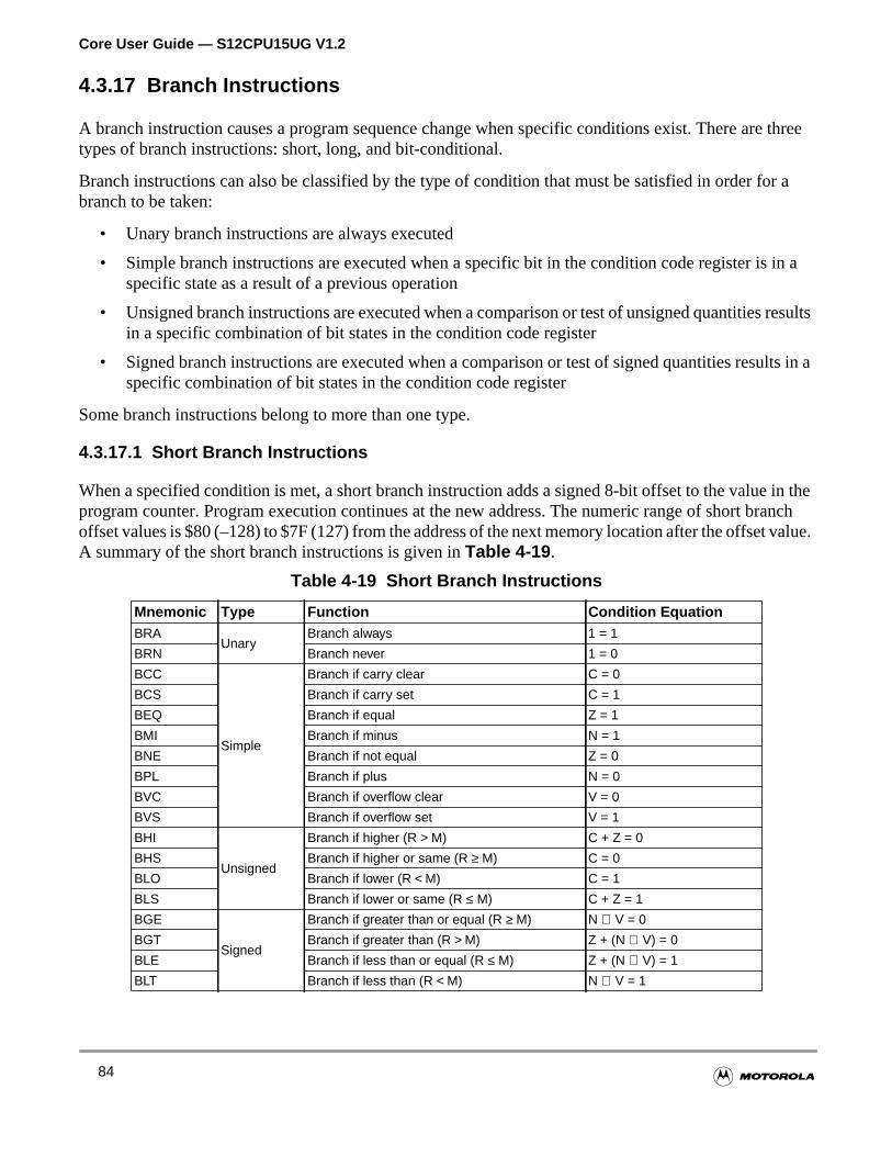
Core User Guide — S12CPU15UG V1.2
e three
or a
in a
results
lts in a
in theranchvalue.
4.3.17 Branch Instructions
A branch instruction causes a program sequence change when specific conditions exist. There artypes of branch instructions: short, long, and bit-conditional.
Branch instructions can also be classified by the type of condition that must be satisfied in order fbranch to be taken:
• Unary branch instructions are always executed
• Simple branch instructions are executed when a specific bit in the condition code register isspecific state as a result of a previous operation
• Unsigned branch instructions are executed when a comparison or test of unsigned quantitiesin a specific combination of bit states in the condition code register
• Signed branch instructions are executed when a comparison or test of signed quantities resuspecific combination of bit states in the condition code register
Some branch instructions belong to more than one type.
4.3.17.1 Short Branch Instructions
When a specified condition is met, a short branch instruction adds a signed 8-bit offset to the valueprogram counter. Program execution continues at the new address. The numeric range of short boffset values is $80 (–128) to $7F (127) from the address of the next memory location after the offsetA summary of the short branch instructions is given inTable 4-19 .
Table 4-19 Short Branch Instructions
Mnemonic Type Function Condition EquationBRA
UnaryBranch always 1 = 1
BRN Branch never 1 = 0
BCC
Simple
Branch if carry clear C = 0
BCS Branch if carry set C = 1
BEQ Branch if equal Z = 1
BMI Branch if minus N = 1
BNE Branch if not equal Z = 0
BPL Branch if plus N = 0
BVC Branch if overflow clear V = 0
BVS Branch if overflow set V = 1
BHI
Unsigned
Branch if higher (R > M) C + Z = 0
BHS Branch if higher or same (R ≥ M) C = 0
BLO Branch if lower (R < M) C = 1
BLS Branch if lower or same (R ≤ M) C + Z = 1
BGE
Signed
Branch if greater than or equal (R ≥ M) N ⊕ V = 0
BGT Branch if greater than (R > M) Z + (N ⊕ V) = 0
BLE Branch if less than or equal (R ≤ M) Z + (N ⊕ V) = 1
BLT Branch if less than (R < M) N ⊕ V = 1
84
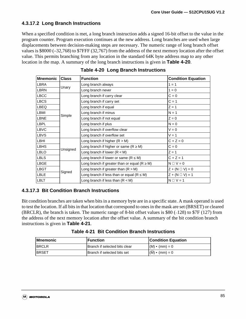
Core User Guide — S12CPU15UG V1.2
in then largeoffsetoffset
er
is usedleared
nch
4.3.17.2 Long Branch Instructions
When a specified condition is met, a long branch instruction adds a signed 16-bit offset to the valueprogram counter. Program execution continues at the new address. Long branches are used whedisplacements between decision-making steps are necessary. The numeric range of long branch values is $8000 (–32,768) to $7FFF (32,767) from the address of the next memory location after thevalue. This permits branching from any location in the standard 64K byte address map to any othlocation in the map. A summary of the long branch instructions is given inTable 4-20 .
4.3.17.3 Bit Condition Branch Instructions
Bit condition branches are taken when bits in a memory byte are in a specific state. A mask operandto test the location. If all bits in that location that correspond to ones in the mask are set (BRSET) or c(BRCLR), the branch is taken. The numeric range of 8-bit offset values is $80 (–128) to $7F (127) fromthe address of the next memory location after the offset value. A summary of the bit condition brainstructions is given inTable 4-21 .
Table 4-20 Long Branch Instructions
Mnemonic Class Function Condition EquationLBRA
UnaryLong branch always 1 = 1
LBRN Long branch never 1 = 0
LBCC
Simple
Long branch if carry clear C = 0
LBCS Long branch if carry set C = 1
LBEQ Long branch if equal Z = 1
LBMI Long branch if minus N = 1
LBNE Long branch if not equal Z = 0
LBPL Long branch if plus N = 0
LBVC Long branch if overflow clear V = 0
LBVS Long branch if overflow set V = 1
LBHI
Unsigned
Long branch if higher (R > M) C + Z = 0
LBHS Long branch if higher or same (R ≥ M) C = 0
LBLO Long branch if lower (R < M) Z = 1
LBLS Long branch if lower or same (R ≤ M) C + Z = 1
LBGE
Signed
Long branch if greater than or equal (R ≥ M) N ⊕ V = 0
LBGT Long branch if greater than (R > M) Z + (N ⊕ V) = 0
LBLE Long branch if less than or equal (R ≤ M) Z + (N ⊕ V) = 1
LBLT Long branch if less than (R < M) N ⊕ V = 1
Table 4-21 Bit Condition Branch Instructions
Mnemonic Function Condition Equation
BRCLR Branch if selected bits clear (M) • (mm) = 0
BRSET Branch if selected bits set (M) • (mm) = 0
85
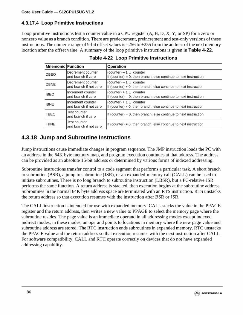
Core User Guide — S12CPU15UG V1.2
orof thesemory
C withaddresssing.
ranchd toRddress.stacks
GEere thexedlue andnstacksCALL.d
4.3.17.4 Loop Primitive Instructions
Loop primitive instructions test a counter value in a CPU register (A, B, D, X, Y, or SP) for a zero nonzero value as a branch condition. There are predecrement, preincrement and test-only versionsinstructions. The numeric range of 9-bit offset values is –256 to +255 from the address of the next melocation after the offset value. A summary of the loop primitive instructions is given inTable 4-22 .
4.3.18 Jump and Subroutine Instructions
Jump instructions cause immediate changes in program sequence. The JMP instruction loads the Pan address in the 64K byte memory map, and program execution continues at that address. The can be provided as an absolute 16-bit address or determined by various forms of indexed addres
Subroutine instructions transfer control to a code segment that performs a particular task. A short bto subroutine (BSR), a jump to subroutine (JSR), or an expanded-memory call (CALL) can be useinitiate subroutines. There is no long branch to subroutine instruction (LBSR), but a PC-relative JSperforms the same function. A return address is stacked, then execution begins at the subroutine aSubroutines in the normal 64K byte address space are terminated with an RTS instruction. RTS unthe return address so that execution resumes with the instruction after BSR or JSR.
The CALL instruction is intended for use with expanded memory. CALL stacks the value in the PPAregister and the return address, then writes a new value to PPAGE to select the memory page whsubroutine resides. The page value is an immediate operand in all addressing modes except indeindirect modes; in these modes, an operand points to locations in memory where the new page vasubroutine address are stored. The RTC instruction ends subroutines in expanded memory. RTC uthe PPAGE value and the return address so that execution resumes with the next instruction afterFor software compatibility, CALL and RTC operate correctly on devices that do not have expandeaddressing capability.
Table 4-22 Loop Primitive Instructions
Mnemonic Function Operation
DBEQDecrement counterand branch if zero
(counter) – 1 ⇒ counterIf (counter) = 0, then branch, else continue to next instruction
DBNEDecrement counterand branch if not zero
(counter) – 1 ⇒ counterIf (counter) ≠ 0, then branch, else continue to next instruction
IBEQIncrement counterand branch if zero
(counter) + 1 ⇒ counterIf (counter) = 0, then branch, else continue to next instruction
IBNEIncrement counterand branch if not zero
(counter) + 1 ⇒ counterIf (counter) ≠ 0, then branch, else continue to next instruction
TBEQTest counterand branch if zero
If (counter) = 0, then branch, else continue to next instruction
TBNETest counterand branch if not zero
If (counter) ≠ 0, then branch, else continue to next instruction
86
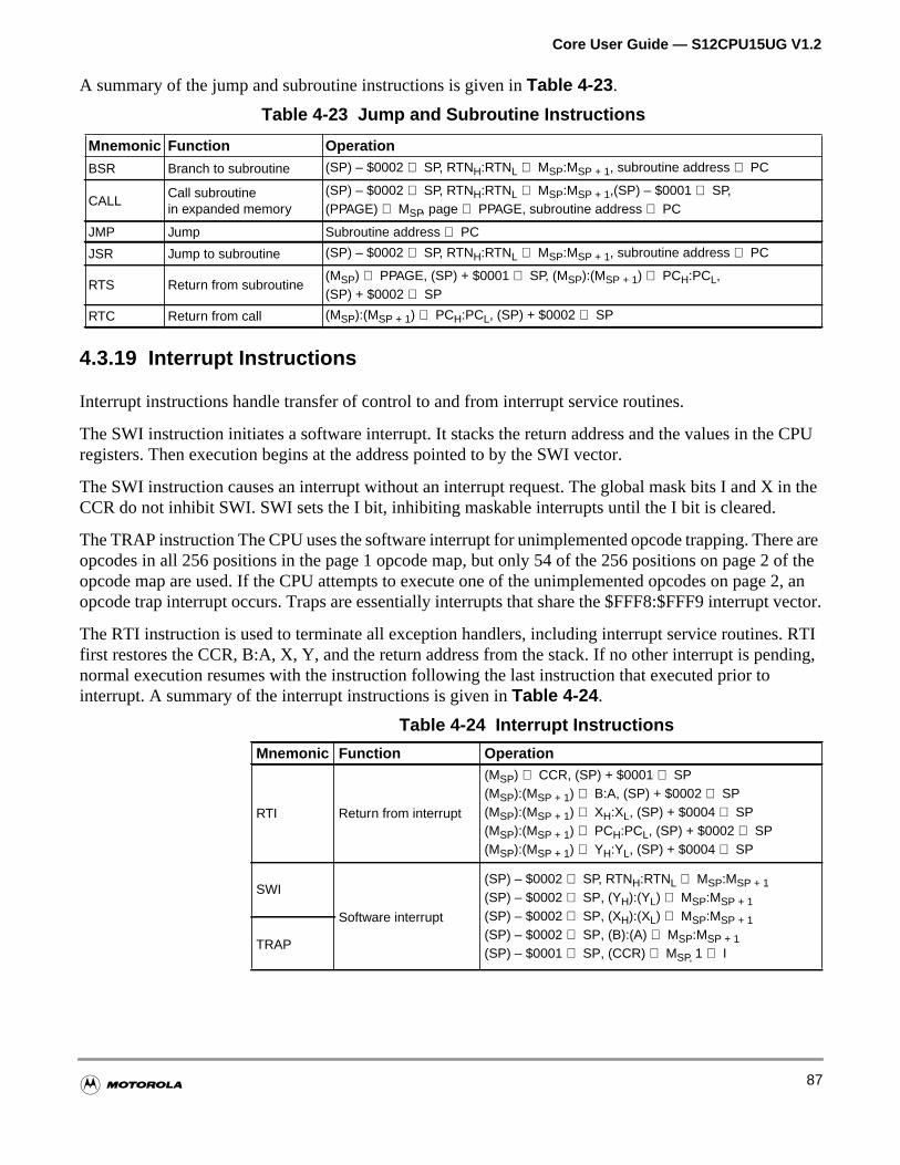
Core User Guide — S12CPU15UG V1.2
e CPU
in the
re are of thee 2, anvector.
. RTInding,
A summary of the jump and subroutine instructions is given inTable 4-23 .
4.3.19 Interrupt Instructions
Interrupt instructions handle transfer of control to and from interrupt service routines.
The SWI instruction initiates a software interrupt. It stacks the return address and the values in thregisters. Then execution begins at the address pointed to by the SWI vector.
The SWI instruction causes an interrupt without an interrupt request. The global mask bits I and XCCR do not inhibit SWI. SWI sets the I bit, inhibiting maskable interrupts until the I bit is cleared.
The TRAP instruction The CPU uses the software interrupt for unimplemented opcode trapping. Theopcodes in all 256 positions in the page 1 opcode map, but only 54 of the 256 positions on page 2opcode map are used. If the CPU attempts to execute one of the unimplemented opcodes on pagopcode trap interrupt occurs. Traps are essentially interrupts that share the $FFF8:$FFF9 interrupt
The RTI instruction is used to terminate all exception handlers, including interrupt service routinesfirst restores the CCR, B:A, X, Y, and the return address from the stack. If no other interrupt is penormal execution resumes with the instruction following the last instruction that executed prior tointerrupt. A summary of the interrupt instructions is given inTable 4-24 .
Table 4-23 Jump and Subroutine Instructions
Mnemonic Function Operation
BSR Branch to subroutine (SP) – $0002 ⇒ SP, RTNH:RTNL ⇒ MSP:MSP + 1, subroutine address ⇒ PC
CALLCall subroutinein expanded memory
(SP) – $0002 ⇒ SP, RTNH:RTNL ⇒ MSP:MSP + 1,(SP) – $0001 ⇒ SP,(PPAGE) ⇒ MSP, page ⇒ PPAGE, subroutine address ⇒ PC
JMP Jump Subroutine address ⇒ PC
JSR Jump to subroutine (SP) – $0002 ⇒ SP, RTNH:RTNL ⇒ MSP:MSP + 1, subroutine address ⇒ PC
RTS Return from subroutine(MSP) ⇒ PPAGE, (SP) + $0001 ⇒ SP, (MSP):(MSP + 1) ⇒ PCH:PCL,(SP) + $0002 ⇒ SP
RTC Return from call (MSP):(MSP + 1) ⇒ PCH:PCL, (SP) + $0002 ⇒ SP
Table 4-24 Interrupt Instructions
Mnemonic Function Operation
RTI Return from interrupt
(MSP) ⇒ CCR, (SP) + $0001 ⇒ SP(MSP):(MSP + 1) ⇒ B:A, (SP) + $0002 ⇒ SP(MSP):(MSP + 1) ⇒ XH:XL, (SP) + $0004 ⇒ SP(MSP):(MSP + 1) ⇒ PCH:PCL, (SP) + $0002 ⇒ SP(MSP):(MSP + 1) ⇒ YH:YL, (SP) + $0004 ⇒ SP
SWI
Software interrupt
(SP) – $0002 ⇒ SP, RTNH:RTNL ⇒ MSP:MSP + 1(SP) – $0002 ⇒ SP, (YH):(YL) ⇒ MSP:MSP + 1(SP) – $0002 ⇒ SP, (XH):(XL) ⇒ MSP:MSP + 1(SP) – $0002 ⇒ SP, (B):(A) ⇒ MSP:MSP + 1(SP) – $0001 ⇒ SP, (CCR) ⇒ MSP, 1 ⇒ I
TRAP
87
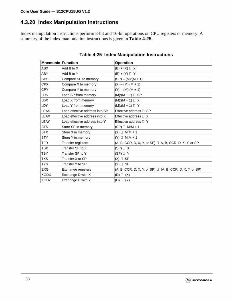
Core User Guide — S12CPU15UG V1.2
A
4.3.20 Index Manipulation Instructions
Index manipulation instructions perform 8-bit and 16-bit operations on CPU registers or memory. summary of the index manipulation instructions is given inTable 4-25 .
Table 4-25 Index Manipulation Instructions
Mnemonic Function OperationABX Add B to X (B) + (X) ⇒ X
ABY Add B to Y (B) + (Y) ⇒ Y
CPS Compare SP to memory (SP) – (M):(M + 1)
CPX Compare X to memory (X) – (M):(M + 1)
CPY Compare Y to memory (Y) – (M):(M + 1)
LDS Load SP from memory (M):(M + 1) ⇒ SP
LDX Load X from memory (M):(M + 1) ⇒ X
LDY Load Y from memory (M):(M + 1) ⇒ Y
LEAS Load effective address into SP Effective address ⇒ SP
LEAX Load effective address into X Effective address ⇒ X
LEAY Load effective address into Y Effective address ⇒ Y
STS Store SP in memory (SP) ⇒ M:M + 1
STX Store X in memory (X) ⇒ M:M + 1
STY Store Y in memory (Y) ⇒ M:M + 1
TFR Transfer registers (A, B, CCR, D, X, Y, or SP) ⇒ A, B, CCR, D, X, Y, or SP
TSX Transfer SP to X (SP) ⇒ X
TSY Transfer SP to Y (SP) ⇒ Y
TXS Transfer X to SP (X) ⇒ SP
TYS Transfer Y to SP (Y) ⇒ SP
EXG Exchange registers (A, B, CCR, D, X, Y, or SP) ⇔ (A, B, CCR, D, X, Y, or SP)
XGDX Exchange D with X (D) ⇔ (X)
XGDY Exchange D with Y (D) ⇔ (Y)
88
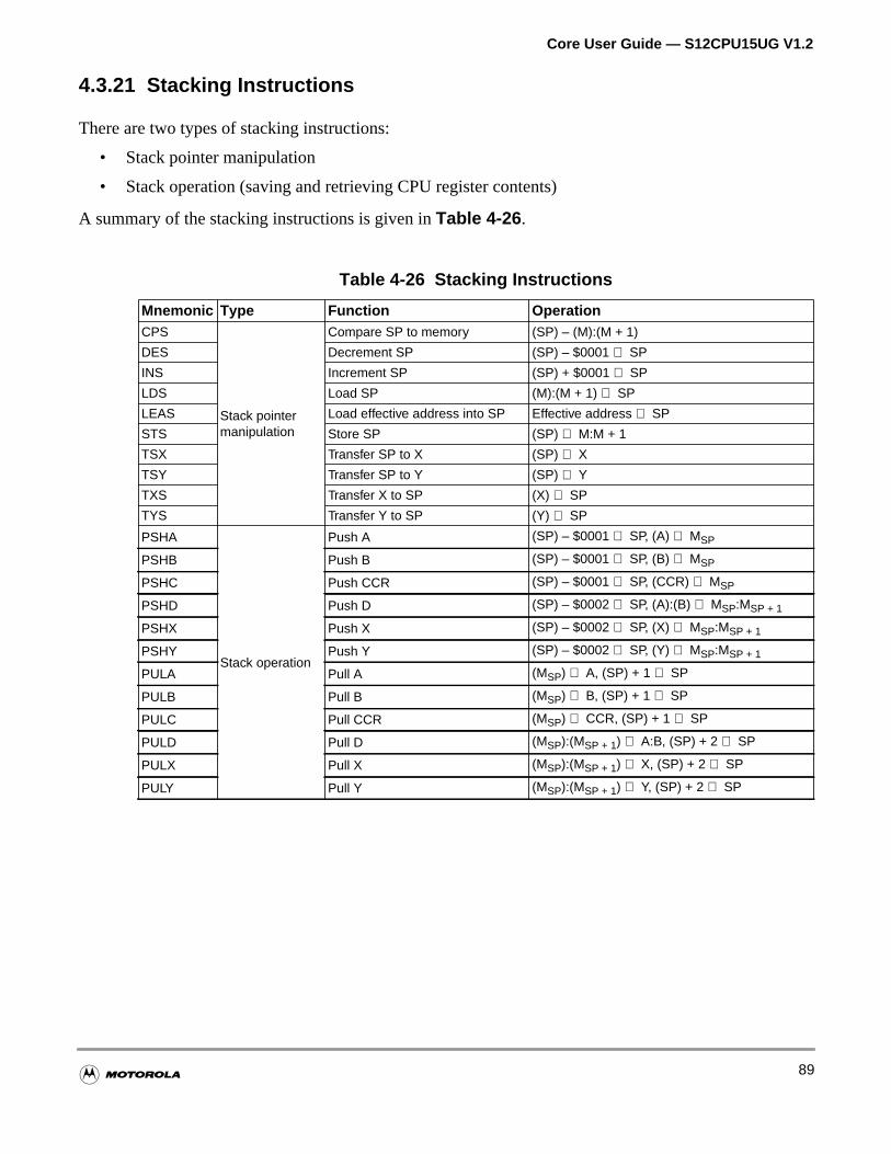
Core User Guide — S12CPU15UG V1.2
4.3.21 Stacking Instructions
There are two types of stacking instructions:
• Stack pointer manipulation
• Stack operation (saving and retrieving CPU register contents)
A summary of the stacking instructions is given inTable 4-26 .
Table 4-26 Stacking Instructions
Mnemonic Type Function OperationCPS
Stack pointermanipulation
Compare SP to memory (SP) – (M):(M + 1)
DES Decrement SP (SP) – $0001 ⇒ SP
INS Increment SP (SP) + $0001 ⇒ SP
LDS Load SP (M):(M + 1) ⇒ SP
LEAS Load effective address into SP Effective address ⇒ SP
STS Store SP (SP) ⇒ M:M + 1
TSX Transfer SP to X (SP) ⇒ X
TSY Transfer SP to Y (SP) ⇒ Y
TXS Transfer X to SP (X) ⇒ SP
TYS Transfer Y to SP (Y) ⇒ SP
PSHA
Stack operation
Push A (SP) – $0001 ⇒ SP, (A) ⇒ MSP
PSHB Push B (SP) – $0001 ⇒ SP, (B) ⇒ MSP
PSHC Push CCR (SP) – $0001 ⇒ SP, (CCR) ⇒ MSP
PSHD Push D (SP) – $0002 ⇒ SP, (A):(B) ⇒ MSP:MSP + 1
PSHX Push X (SP) – $0002 ⇒ SP, (X) ⇒ MSP:MSP + 1
PSHY Push Y (SP) – $0002 ⇒ SP, (Y) ⇒ MSP:MSP + 1
PULA Pull A (MSP) ⇒ A, (SP) + 1 ⇒ SP
PULB Pull B (MSP) ⇒ B, (SP) + 1 ⇒ SP
PULC Pull CCR (MSP) ⇒ CCR, (SP) + 1 ⇒ SP
PULD Pull D (MSP):(MSP + 1) ⇒ A:B, (SP) + 2 ⇒ SP
PULX Pull X (MSP):(MSP + 1) ⇒ X, (SP) + 2 ⇒ SP
PULY Pull Y (MSP):(MSP + 1) ⇒ Y, (SP) + 2 ⇒ SP
89
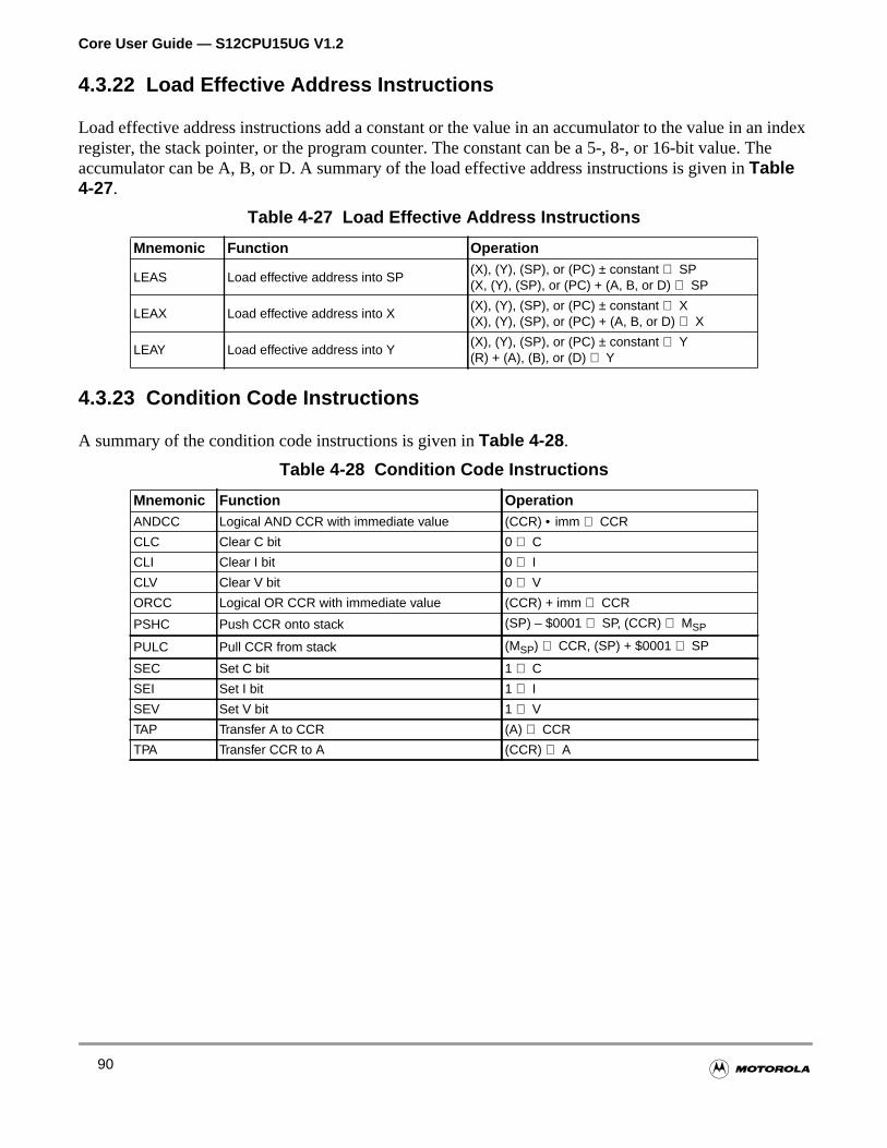
Core User Guide — S12CPU15UG V1.2
indexhe
4.3.22 Load Effective Address Instructions
Load effective address instructions add a constant or the value in an accumulator to the value in anregister, the stack pointer, or the program counter. The constant can be a 5-, 8-, or 16-bit value. Taccumulator can be A, B, or D. A summary of the load effective address instructions is given inTable4-27.
4.3.23 Condition Code Instructions
A summary of the condition code instructions is given inTable 4-28 .
Table 4-27 Load Effective Address Instructions
Mnemonic Function Operation
LEAS Load effective address into SP(X), (Y), (SP), or (PC) ± constant ⇒ SP(X, (Y), (SP), or (PC) + (A, B, or D) ⇒ SP
LEAX Load effective address into X(X), (Y), (SP), or (PC) ± constant ⇒ X(X), (Y), (SP), or (PC) + (A, B, or D) ⇒ X
LEAY Load effective address into Y(X), (Y), (SP), or (PC) ± constant ⇒ Y(R) + (A), (B), or (D) ⇒ Y
Table 4-28 Condition Code Instructions
Mnemonic Function OperationANDCC Logical AND CCR with immediate value (CCR) • imm ⇒ CCR
CLC Clear C bit 0 ⇒ C
CLI Clear I bit 0 ⇒ I
CLV Clear V bit 0 ⇒ V
ORCC Logical OR CCR with immediate value (CCR) + imm ⇒ CCR
PSHC Push CCR onto stack (SP) – $0001 ⇒ SP, (CCR) ⇒ MSP
PULC Pull CCR from stack (MSP) ⇒ CCR, (SP) + $0001 ⇒ SP
SEC Set C bit 1 ⇒ C
SEI Set I bit 1 ⇒ I
SEV Set V bit 1 ⇒ V
TAP Transfer A to CCR (A) ⇒ CCR
TPA Transfer CCR to A (CCR) ⇒ A
90
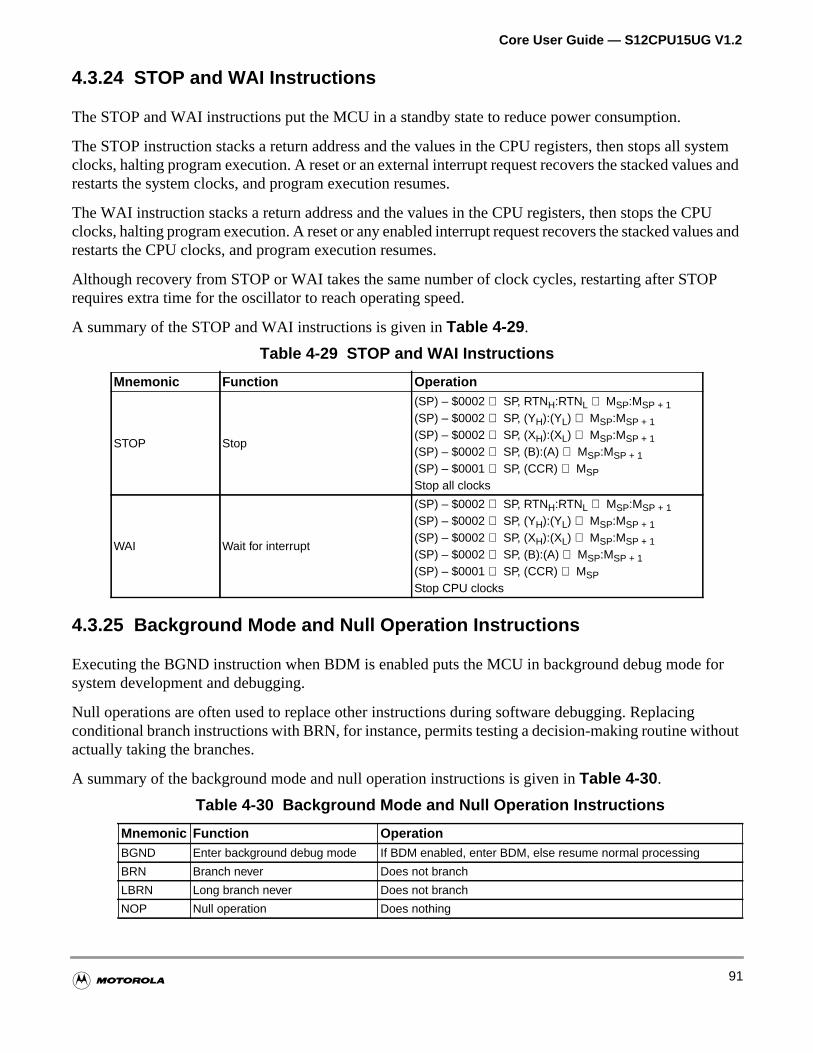
Core User Guide — S12CPU15UG V1.2
systemes and
PUues and
P
for
hout
4.3.24 STOP and WAI Instructions
The STOP and WAI instructions put the MCU in a standby state to reduce power consumption.
The STOP instruction stacks a return address and the values in the CPU registers, then stops all clocks, halting program execution. A reset or an external interrupt request recovers the stacked valurestarts the system clocks, and program execution resumes.
The WAI instruction stacks a return address and the values in the CPU registers, then stops the Cclocks, halting program execution. A reset or any enabled interrupt request recovers the stacked valrestarts the CPU clocks, and program execution resumes.
Although recovery from STOP or WAI takes the same number of clock cycles, restarting after STOrequires extra time for the oscillator to reach operating speed.
A summary of the STOP and WAI instructions is given inTable 4-29 .
4.3.25 Background Mode and Null Operation Instructions
Executing the BGND instruction when BDM is enabled puts the MCU in background debug modesystem development and debugging.
Null operations are often used to replace other instructions during software debugging. Replacingconditional branch instructions with BRN, for instance, permits testing a decision-making routine witactually taking the branches.
A summary of the background mode and null operation instructions is given inTable 4-30 .
Table 4-29 STOP and WAI Instructions
Mnemonic Function Operation
STOP Stop
(SP) – $0002 ⇒ SP, RTNH:RTNL ⇒ MSP:MSP + 1(SP) – $0002 ⇒ SP, (YH):(YL) ⇒ MSP:MSP + 1(SP) – $0002 ⇒ SP, (XH):(XL) ⇒ MSP:MSP + 1(SP) – $0002 ⇒ SP, (B):(A) ⇒ MSP:MSP + 1(SP) – $0001 ⇒ SP, (CCR) ⇒ MSPStop all clocks
WAI Wait for interrupt
(SP) – $0002 ⇒ SP, RTNH:RTNL ⇒ MSP:MSP + 1(SP) – $0002 ⇒ SP, (YH):(YL) ⇒ MSP:MSP + 1(SP) – $0002 ⇒ SP, (XH):(XL) ⇒ MSP:MSP + 1(SP) – $0002 ⇒ SP, (B):(A) ⇒ MSP:MSP + 1(SP) – $0001 ⇒ SP, (CCR) ⇒ MSPStop CPU clocks
Table 4-30 Background Mode and Null Operation Instructions
Mnemonic Function OperationBGND Enter background debug mode If BDM enabled, enter BDM, else resume normal processing
BRN Branch never Does not branch
LBRN Long branch never Does not branch
NOP Null operation Does nothing
91
Core User Guide — S12CPU15UG V1.2
ativece
ousten in
uction2 were
rt forortC11
ble iny used16-bit
U canlowsw forlong
uch ased to
d local
nterexed
the D
s andnation6-bit
4.4 High-Level Language Support
Many programmers are turning to high-level languages such as C as an alternative to coding in nassembly languages. High-level language (HLL) programming can improve productivity and producode that is more easily maintained than assembly language programs. Historically, the most seridrawback to the use of HLL in microcontrollers has been the relatively large size of programs writHLL. Larger program memory space size requirements translate into increased system costs.
Motorola solicited the cooperation of third-party software developers to assure that the HCS12 instrset would meet the needs of a more efficient generation of compilers. Several features of the HCS1specifically designed to improve the efficiency of compiled HLL, and thus minimize cost.
This subsection identifies HCS12 instructions and addressing modes that provide improved suppohigh-level language. C language examples are provided to demonstrate how these features suppefficient HLL structures and concepts. Since the HCS12 instruction set is a superset of the M68Hinstruction set, some of the discussions use the M68HC11 as a basis for comparison.
4.4.1 Data Types
The HCS12 CPU supports the bit-sized data type with bit-manipulation instructions that are availaextended, direct, and indexed variations. The char data type is a simple 8-bit value that is commonlto specify variables in a small microcontroller system because it requires less memory space than ainteger (provided the variable has a range small enough to fit into eight bits). The 16-bit HCS12 CPeasily handle 16-bit integer types and the set of conditional branches, including long branches, albranching based on signed or unsigned arithmetic results. Some of the higher math functions allodivision and multiplication involving 32-bit values, although it is somewhat less common to use suchvalues in a microcontroller system.
Special sign-extension instructions allow easy type-casting from smaller data types to larger ones, sfrom char to integer. This sign extension is automatically performed when an 8-bit value is transferra 16-bit register.
4.4.2 Parameters and Variables
High-level languages make extensive use of the stack, both to pass variables and for temporary anstorage. It follows that there should be easy ways to push and pull all CPU registers, that stackpointer-based indexing should be allowed, and that direct arithmetic manipulation of the stack poivalue should be allowed. The HCS12 instruction set provides for all of these needs with improved indaddressing, the addition of an LEAS instruction, and the addition of push and pull instructions for accumulator and the CCR.
4.4.2.1 Register Pushes and Pulls
The M68HC11 has push and pull instructions for A, B, X, and Y, but requires separate 8-bit pushepulls of accumulators A and B to stack or unstack the 16-bit D accumulator (the concatenated combiA:B). The PSHD and PULD instructions allow directly stacking the D accumulator in the expected 1order.
92
Core User Guide — S12CPU15UG V1.2
thate CCR
bles:
eightis usedm –8interes than
frameriablesp and
a JSRer offrame
ted forbles.
ffsets.waysationsmetersto
exedr to
n settionsected
Adding PSHC and PULC improved orthogonality by completing the set of stacking instructions soany of the CPU registers can be pushed or pulled. These instructions are also useful for preserving thvalue during a function call subroutine.
4.4.2.2 Allocating and Deallocating Stack Space
The LEAS instruction can be used to allocate or deallocate space on the stack for temporary varia
LEAS –10,S ;Allocate space for 5 16-bit integers
LEAS 10,S ;Deallocate space for 5 16-bit ints
The (de)allocation can even be combined with a register push or pull as in the following example:
LDX 8,S+ ;Load return value and deallocate
X is loaded with the 16-bit integer value at the top of the stack, and the stack pointer is adjusted up byto deallocate space for eight bytes’ worth of temporary storage. Postincrement indexed addressingin this example, but all four combinations of pre/post increment/decrement are available (offsets froto +8 inclusive, from X, Y, or SP). This form of indexing can often be used to get an index or stack poadjustment for free during an indexed operation: the instruction requires no more code space or cycla zero-offset indexed instruction.
4.4.2.3 Frame Pointer
In the C language, it is common to have a frame pointer in addition to the CPU stack pointer. Theis an area of memory within the system stack which is used for parameters and local storage of vaused within a function subroutine. The following is a description of how a frame pointer can be set uused.
First, parameters (typically values in CPU registers) are pushed onto the system stack prior to usingor CALL to get to the function subroutine. At the beginning of the called subroutine, the frame pointthe calling program is pushed onto the stack. Typically, an index register, such as X, is used as thepointer, so a PSHX instruction would save the frame pointer from the calling program.
Next, the called subroutine establishes a new frame pointer by executing a TFR S,X. Space is allocalocal variables by executing an LEAS –n,S, where n is the number of bytes needed for local varia
Notice that parameters are at positive offsets from the frame pointer while locals are at negative oIn the M68HC11, the indexed addressing mode uses only positive offsets, so the frame pointer alpoints to the lowest address of any parameter or local. After the function subroutine finishes, calculare required to restore the stack pointer to the midframe position between the locals and the parabefore returning to the calling program. The HCS12 CPU requires only the execution of TFR X,S deallocate the local storage and return.
The concept of a frame pointer is supported in the HCS12 through a combination of improved indaddressing, universal transfer/exchange, and the LEA instruction. These instructions work togetheachieve more efficient handling of frame pointers. It is important to consider the complete instructioas a complex system with subtle interrelationships rather than simply examining individual instrucwhen trying to improve an instruction set. Adding or removing a single instruction can have unexpconsequences.
93
Core User Guide — S12CPU15UG V1.2
12
a
harigned
toauset at
uce a
DIVS,mpilerneedion.
betrmed asent if
te theecificbasedoffset a
4.4.3 Increment and Decrement Operators
In C, the notation+ + i or i – – is often used to form loop counters. Within limited constraints, the HCSloop primitives can speed up the loop-count-and-branch function.
The HCS12 includes a set of six basic loop-control instructions that decrement, increment, or testloop-count register and then branch if the register is either equal to zero or not equal to zero. Theloop-count register can be A, B, D, X, Y, or SP. A or B could be used if the loop count fits in an 8-bit cvariable; the other choices are all 16-bit registers. The relative offset for the loop branch is a 9-bit svalue, so these instructions can be used with loops as long as 256 bytes.
In some cases, the pre- or postincrement operation can be combined with an indexed instruction eliminate the cost of the increment operation. This is typically done by postcompile optimization becthe indexed instruction that could absorb the increment/decrement operation may not be apparencompile time.
4.4.4 Higher Math Functions
In the HCS12 CPU, subtle characteristics of higher math operations such as IDIVS and EMUL arearranged so a compiler can handle inputs and outputs more efficiently.
The most apparent case is the IDIVS instruction, which divides two 16-bit signed numbers to prod16-bit result. While the same function can be accomplished with the EDIVS instruction (a 32 by 16divide), doing so is much less efficient because extra steps are required to prepare inputs to the Eand because EDIVS uses the Y index register. EDIVS uses a 32-bit signed numerator and the C cowould typically want to use a 16-bit value (the size of an integer data type). The 16-bit C value wouldto be sign-extended into the upper 16-bits of the 32-bit EDIVS numerator before the divide operat
Operand size is also a potential problem in the extended multiply operations but the difficulty can minimized by putting the results in CPU registers. Having higher-precision math instructions is nonecessarily a requirement for supporting high-level language because these functions can be perfolibrary functions. However, if an application requires these functions, the code is much more efficithe CPU can use native instructions instead of relatively large, slow routines.
4.4.5 Conditional If Constructs
In the HCS12 instruction set, most arithmetic and data manipulation instructions automatically updacondition code register, unlike other architectures that only change condition codes during a few spcompare instructions. The HCS12 includes branch instructions that perform conditional branchingon the state of the indicators in the condition code register. Short branches use a single byte-relativethat allows branching to a destination within about±128 locations from the branch. Long branches use16-bit relative offset that allows conditional branching to any location in the 64K byte map.
94
Core User Guide — S12CPU15UG V1.2
sing tofset
,
e thanheis thate to a
has tos with
ationack and, this
havingto know
thatits oldcalledccess
ll. The
of
de,ignedkes it
4.4.6 Case and Switch Statements
Case and switch statements (and computed GOTOs) can use PC-relative indexed-indirect addresdetermine which path to take. Depending upon the situation, cases can use either the constant ofvariation or the accumulator D offset variation of indexed-indirect addressing.
4.4.7 Pointers
The HCS12 supports pointers with direct arithmetic operations on the 16-bit index registers (LEASLEAX, and LEAY instructions) and with indexed-indirect addressing modes.
4.4.8 Function Calls
Bank switching is a common way of adapting a CPU with a 16-bit address bus to accommodate mor64K bytes of program memory space. One of the most significant drawbacks of this technique is trequirement of masking interrupts while the bank page value is being changed. Another problem the physical location of the bank page register can change from one system to another or even duchange to mapping controls by a user program. In these situations, an operating system programkeep track of the physical location of the page register. The HCS12 addresses both of these problemthe uninterruptible CALL and return from call (RTC) instructions.
The CALL instruction is similar to a JSR instruction, except that the programmer supplies a destinpage value as part of the instruction. When CALL executes, the old page value is saved on the stthe new page value is written to the bank page register. Since the CALL instruction is uninterruptibleeliminates the need to separately mask off interrupts during the context switch.
The HCS12 has dedicated signal lines that allow the CPU to access the bank page register withoutto use an address in the normal 64K byte address space. This eliminates the need for the programwhere the page register is physically located.
The RTC instruction is similar to the RTS instruction, except that RTC uses the byte of informationwas saved on the stack by the corresponding CALL instruction to restore the bank page register tovalue. A CALL/RTC pair can be used to access any function subroutine on any page. But when thesubroutine is on the current page or in an area of memory that is always visible, it is more efficient to ait with JSR/RTS instructions.
Push and pull instructions can be used to stack some or all the CPU registers during a function caHCS12 CPU can push and pull any of the CPU registers A, B, D, CCR, X, Y, or SP.
4.4.9 Instruction Set Orthogonality
One very helpful aspect of the HCS12 instruction set, orthogonality, is difficult to quantify in termsdirect benefit to an HLL compiler. Orthogonality refers to the regularity of the instruction set. Acompletely orthogonal instruction set would allow any instruction to operate in any addressing mowould have identical code sizes and execution times for similar operations, and would include both sand unsigned versions of all mathematical instructions. Greater regularity of the instruction set ma
95

Core User Guide — S12CPU15UG V1.2
pecial
possible to implement compilers more efficiently because operation is more consistent, and fewer scases must be handled.96
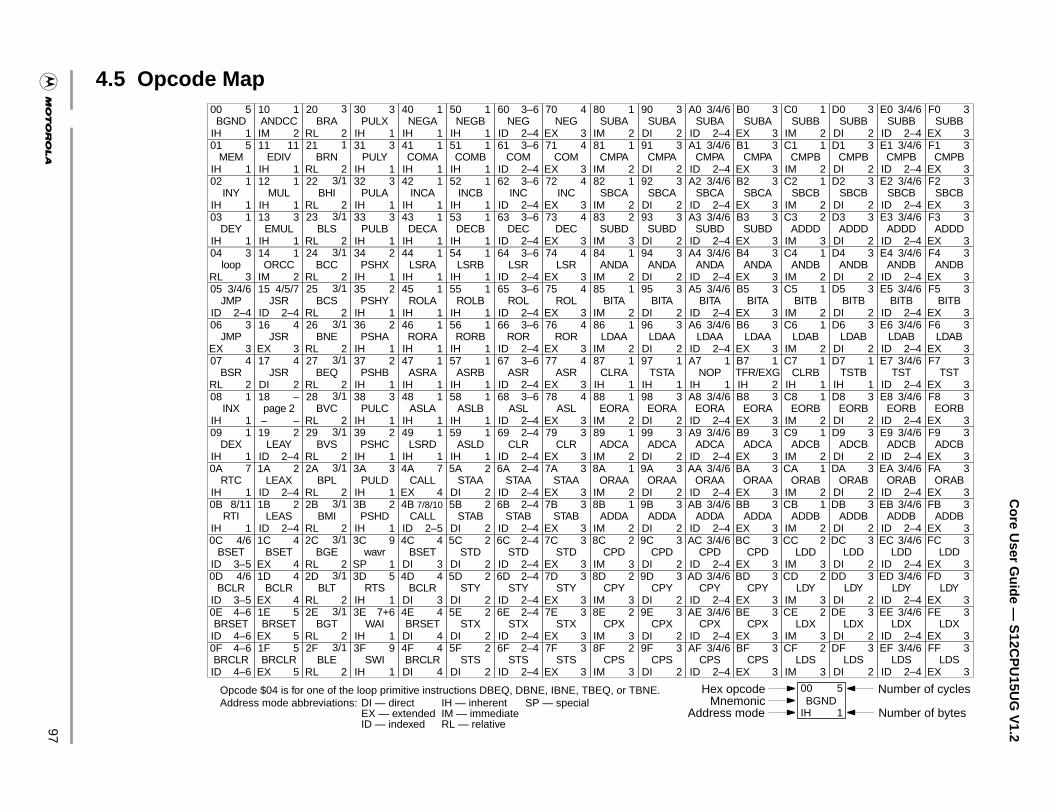
97
Core U
ser Guide —
S12C
PU
15UG
V1.2
BA3
3SUBB
1C0
IM 2SUBB
3D0
DI 2SUBB
3/4/6E0
ID 2–4SUBB
3F0
EX 3
PA3
3CMPB
1C1
IM 2CMPB
3D1
DI 2CMPB
3/4/6E1
ID 2–4CMPB
3F1
EX 3
CA3
3SBCB
1C2
IM 2SBCB
3D2
DI 2SBCB
3/4/6E2
ID 2–4SBCB
3F2
EX 3
BD3
3ADDD
2C3
IM 3ADDD
3D3
DI 2ADDD
3/4/6E3
ID 2–4ADDD
3F3
EX 3
DA3
3ANDB
1C4
IM 2ANDB
3D4
DI 2ANDB
3/4/6E4
ID 2–4ANDB
3F4
EX 3
TA3
3BITB
1C5
IM 2BITB
3D5
DI 2BITB
3/4/6E5
ID 2–4BITB
3F5
EX 3
AA3
3LDAB
1C6
IM 2LDAB
3D6
DI 2LDAB
3/4/6E6
ID 2–4LDAB
3F6
EX 3
/EXG1
2CLRB
1C7
IH 1TSTB
1D7
IH 1TST
3/4/6E7
ID 2–4TST
3F7
EX 3
RA3
3EORB
1C8
IM 2EORB
3D8
DI 2EORB
3/4/6E8
ID 2–4EORB
3F8
EX 3
CA3
3ADCB
1C9
IM 2ADCB
3D9
DI 2ADCB
3/4/6E9
ID 2–4ADCB
3F9
EX 3
AA3
3ORAB
1CA
IM 2ORAB
3DA
DI 2ORAB
3/4/6EA
ID 2–4ORAB
3FA
EX 3
DA3
3ADDB
1CB
IM 2ADDB
3DB
DI 2ADDB
3/4/6EB
ID 2–4ADDB
3FB
EX 3
PD3
3LDD
2CC
IM 3LDD
3DC
DI 2LDD
3/4/6EC
ID 2–4LDD
3FC
EX 3
PY3
3LDY
2CD
IM 3LDY
3DD
DI 2LDY
3/4/6ED
ID 2–4LDY
3FD
EX 3
PX3
3LDX
2CE
IM 3LDX
3DE
DI 2LDX
3/4/6EE
ID 2–4LDX
3FE
EX 3
PS3
3LDS
2CF
IM 3LDS
3DF
DI 2LDS
3/4/6EF
ID 2–4LDS
3FF
EX 3
eic
Number of cycles00BGND
IH
5
Number of bytese 1
4.5 Opcode Map
BGND500
IH 1ANDCC
110
IM 2BRA
320
RL 2PULX
330
IH 1NEGA
140
IH 1NEGB
150
IH 1NEG
3–660
ID 2–4NEG
470
EX 3SUBA
180
IM 2SUBA
390
DI 2SUBA
3/4/6A0
ID 2–4SU
B0
EX
MEM501
IH 1EDIV
1111
IH 1BRN
121
RL 2PULY
331
IH 1COMA
141
IH 1COMB
151
IH 1COM
3–661
ID 2–4COM
471
EX 3CMPA
181
IM 2CMPA
391
DI 2CMPA
3/4/6A1
ID 2–4CM
B1
EX
INY102
IH 1MUL
112
IH 1BHI
3/122
RL 2PULA
332
IH 1INCA
142
IH 1INCB
152
IH 1INC
3–662
ID 2–4INC
472
EX 3SBCA
182
IM 2SBCA
392
DI 2SBCA
3/4/6A2
ID 2–4SB
B2
EX
DEY103
IH 1EMUL
313
IH 1BLS
3/123
RL 2PULB
333
IH 1DECA
143
IH 1DECB
153
IH 1DEC
3–663
ID 2–4DEC
473
EX 3SUBD
283
IM 3SUBD
393
DI 2SUBD
3/4/6A3
ID 2–4SU
B3
EX
loop304
RL 3ORCC
114
IM 2BCC
3/124
RL 2PSHX
234
IH 1LSRA
144
IH 1LSRB
154
IH 1LSR
3–664
ID 2–4LSR
474
EX 3ANDA
184
IM 2ANDA
394
DI 2ANDA
3/4/6A4
ID 2–4AN
B4
EX
JMP3/4/605
ID 2–4JSR
4/5/715
ID 2–4BCS
3/125
RL 2PSHY
235
IH 1ROLA
145
IH 1ROLB
155
IH 1ROL
3–665
ID 2–4ROL
475
EX 3BITA
185
IM 2BITA
395
DI 2BITA
3/4/6A5
ID 2–4BI
B5
EX
JMP306
EX 3JSR
416
EX 3BNE
3/126
RL 2PSHA
236
IH 1RORA
146
IH 1RORB
156
IH 1ROR
3–666
ID 2–4ROR
476
EX 3LDAA
186
IM 2LDAA
396
DI 2LDAA
3/4/6A6
ID 2–4LD
B6
EX
BSR407
RL 2JSR
417
DI 2BEQ
3/127
RL 2PSHB
237
IH 1ASRA
147
IH 1ASRB
157
IH 1ASR
3–667
ID 2–4ASR
477
EX 3CLRA
187
IH 1TSTA
197
IH 1NOP
1A7
IH 1TFRB7
IH
INX108
IH 1page 2
–18
– –BVC
3/128
RL 2PULC
338
IH 1ASLA
148
IH 1ASLB
158
IH 1ASL
3–668
ID 2–4ASL
478
EX 3EORA
188
IM 2EORA
398
DI 2EORA
3/4/6A8
ID 2–4EO
B8
EX
DEX109
IH 1LEAY
219
ID 2–4BVS
3/129
RL 2PSHC
239
IH 1LSRD
149
IH 1ASLD
159
IH 1CLR
2–469
ID 2–4CLR
379
EX 3ADCA
189
IM 2ADCA
399
DI 2ADCA
3/4/6A9
ID 2–4AD
B9
EX
RTC70A
IH 1LEAX
21A
ID 2–4BPL
3/12A
RL 2PULD
33A
IH 1CALL
74A
EX 4STAA
25A
DI 2STAA
2–46A
ID 2–4STAA
37A
EX 3ORAA
18A
IM 2ORAA
39A
DI 2ORAA
3/4/6AA
ID 2–4OR
BA
EX
RTI8/110B
IH 1LEAS
21B
ID 2–4BMI
3/12B
RL 2PSHD
23B
IH 1CALL
7/8/104B
ID 2–5STAB
25B
DI 2STAB
2–46B
ID 2–4STAB
37B
EX 3ADDA
18B
IM 2ADDA
39B
DI 2ADDA
3/4/6AB
ID 2–4AD
BB
EX
BSET4/60C
ID 3–5BSET
41C
EX 4BGE
3/12C
RL 2wavr
93C
SP 1BSET
44C
DI 3STD
25C
DI 2STD
2–46C
ID 2–4STD
37C
EX 3CPD
28C
IM 3CPD
39C
DI 2CPD
3/4/6AC
ID 2–4C
BC
EX
BCLR4/60D
ID 3–5BCLR
41D
EX 4BLT
3/12D
RL 2RTS
53D
IH 1BCLR
44D
DI 3STY
25D
DI 2STY
2–46D
ID 2–4STY
37D
EX 3CPY
28D
IM 3CPY
39D
DI 2CPY
3/4/6AD
ID 2–4C
BD
EX
BRSET4–60E
ID 4–6BRSET
51E
EX 5BGT
3/12E
RL 2WAI
7+63E
IH 1BRSET
44E
DI 4STX
25E
DI 2STX
2–46E
ID 2–4STX
37E
EX 3CPX
28E
IM 3CPX
39E
DI 2CPX
3/4/6AE
ID 2–4C
BE
EX
BRCLR4–60F
ID 4–6BRCLR
51F
EX 5BLE
3/12F
RL 2SWI
93F
IH 1BRCLR
44F
DI 4STS
25F
DI 2STS
2–46F
ID 2–4STS
37F
EX 3CPS
28F
IM 3CPS
39F
DI 2CPS
3/4/6AF
ID 2–4C
BF
EX
Hex opcodMnemon
Address mod
Opcode $04 is for one of the loop primitive instructions DBEQ, DBNE, IBNE, TBEQ, or TBNE.Address mode abbreviations: DI — direct
EX — extendedID — indexed
IH — inherentIM — immediateRL — relative
SP — special
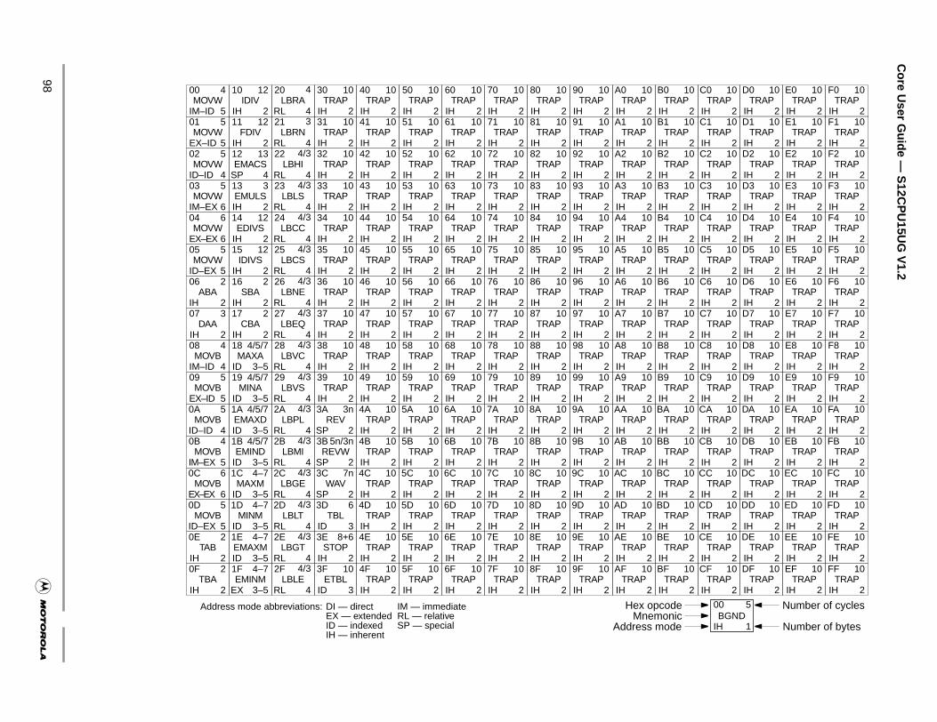
Core U
ser Guide —
S12C
PU
15UG
V1.2
98
AP10
2TRAP
10C0
IH 2TRAP
10D0
IH 2TRAP
10E0
IH 2TRAP
10F0
IH 2
AP10
2TRAP
10C1
IH 2TRAP
10D1
IH 2TRAP
10E1
IH 2TRAP
10F1
IH 2
AP10
2TRAP
10C2
IH 2TRAP
10D2
IH 2TRAP
10E2
IH 2TRAP
10F2
IH 2
AP10
2TRAP
10C3
IH 2TRAP
10D3
IH 2TRAP
10E3
IH 2TRAP
10F3
IH 2
AP10
2TRAP
10C4
IH 2TRAP
10D4
IH 2TRAP
10E4
IH 2TRAP
10F4
IH 2
AP10
2TRAP
10C5
IH 2TRAP
10D5
IH 2TRAP
10E5
IH 2TRAP
10F5
IH 2
AP10
2TRAP
10C6
IH 2TRAP
10D6
IH 2TRAP
10E6
IH 2TRAP
10F6
IH 2
AP10
2TRAP
10C7
IH 2TRAP
10D7
IH 2TRAP
10E7
IH 2TRAP
10F7
IH 2
AP10
2TRAP
10C8
IH 2TRAP
10D8
IH 2TRAP
10E8
IH 2TRAP
10F8
IH 2
AP10
2TRAP
10C9
IH 2TRAP
10D9
IH 2TRAP
10E9
IH 2TRAP
10F9
IH 2
AP10
2TRAP
10CA
IH 2TRAP
10DA
IH 2TRAP
10EA
IH 2TRAP
10FA
IH 2
AP10
2TRAP
10CB
IH 2TRAP
10DB
IH 2TRAP
10EB
IH 2TRAP
10FB
IH 2
AP10
2TRAP
10CC
IH 2TRAP
10DC
IH 2TRAP
10EC
IH 2TRAP
10FC
IH 2
AP10
2TRAP
10CD
IH 2TRAP
10DD
IH 2TRAP
10ED
IH 2TRAP
10FD
IH 2
AP10
2TRAP
10CE
IH 2TRAP
10DE
IH 2TRAP
10EE
IH 2TRAP
10FE
IH 2
AP10
2TRAP
10CF
IH 2TRAP
10DF
IH 2TRAP
10EF
IH 2TRAP
10FF
IH 2
eic
Number of cycles00BGND
IH
5
Number of bytese 1
MOVW400
IM–ID 5IDIV
1210
IH 2LBRA
420
RL 4TRAP
1030
IH 2TRAP
1040
IH 2TRAP
1050
IH 2TRAP
1060
IH 2TRAP
1070
IH 2TRAP
1080
IH 2TRAP
1090
IH 2TRAP
10A0
IH 2TR
B0
IH
MOVW501
EX–ID 5FDIV
1211
IH 2LBRN
321
RL 4TRAP
1031
IH 2TRAP
1041
IH 2TRAP
1051
IH 2TRAP
1061
IH 2TRAP
1071
IH 2TRAP
1081
IH 2TRAP
1091
IH 2TRAP
10A1
IH 2TR
B1
IH
MOVW502
ID–ID 4EMACS
1312
SP 4LBHI
4/322
RL 4TRAP
1032
IH 2TRAP
1042
IH 2TRAP
1052
IH 2TRAP
1062
IH 2TRAP
1072
IH 2TRAP
1082
IH 2TRAP
1092
IH 2TRAP
10A2
IH 2TR
B2
IH
MOVW503
IM–EX 6EMULS
313
IH 2LBLS
4/323
RL 4TRAP
1033
IH 2TRAP
1043
IH 2TRAP
1053
IH 2TRAP
1063
IH 2TRAP
1073
IH 2TRAP
1083
IH 2TRAP
1093
IH 2TRAP
10A3
IH 2TR
B3
IH
MOVW604
EX–EX 6EDIVS
1214
IH 2LBCC
4/324
RL 4TRAP
1034
IH 2TRAP
1044
IH 2TRAP
1054
IH 2TRAP
1064
IH 2TRAP
1074
IH 2TRAP
1084
IH 2TRAP
1094
IH 2TRAP
10A4
IH 2TR
B4
IH
MOVW505
ID–EX 5IDIVS
1215
IH 2LBCS
4/325
RL 4TRAP
1035
IH 2TRAP
1045
IH 2TRAP
1055
IH 2TRAP
1065
IH 2TRAP
1075
IH 2TRAP
1085
IH 2TRAP
1095
IH 2TRAP
10A5
IH 2TR
B5
IH
ABA206
IH 2SBA
216
IH 2LBNE
4/326
RL 4TRAP
1036
IH 2TRAP
1046
IH 2TRAP
1056
IH 2TRAP
1066
IH 2TRAP
1076
IH 2TRAP
1086
IH 2TRAP
1096
IH 2TRAP
10A6
IH 2TR
B6
IH
DAA307
IH 2CBA
217
IH 2LBEQ
4/327
RL 4TRAP
1037
IH 2TRAP
1047
IH 2TRAP
1057
IH 2TRAP
1067
IH 2TRAP
1077
IH 2TRAP
1087
IH 2TRAP
1097
IH 2TRAP
10A7
IH 2TR
B7
IH
MOVB408
IM–ID 4MAXA
4/5/718
ID 3–5LBVC
4/328
RL 4TRAP
1038
IH 2TRAP
1048
IH 2TRAP
1058
IH 2TRAP
1068
IH 2TRAP
1078
IH 2TRAP
1088
IH 2TRAP
1098
IH 2TRAP
10A8
IH 2TR
B8
IH
MOVB509
EX–ID 5MINA
4/5/719
ID 3–5LBVS
4/329
RL 4TRAP
1039
IH 2TRAP
1049
IH 2TRAP
1059
IH 2TRAP
1069
IH 2TRAP
1079
IH 2TRAP
1089
IH 2TRAP
1099
IH 2TRAP
10A9
IH 2TR
B9
IH
MOVB50A
ID–ID 4EMAXD
4/5/71A
ID 3–5LBPL
4/32A
RL 4REV
3n3A
SP 2TRAP
104A
IH 2TRAP
105A
IH 2TRAP
106A
IH 2TRAP
107A
IH 2TRAP
108A
IH 2TRAP
109A
IH 2TRAP
10AA
IH 2TR
BA
IH
MOVB40B
IM–EX 5EMIND
4/5/71B
ID 3–5LBMI
4/32B
RL 4REVW
5n/3n3B
SP 2TRAP
104B
IH 2TRAP
105B
IH 2TRAP
106B
IH 2TRAP
107B
IH 2TRAP
108B
IH 2TRAP
109B
IH 2TRAP
10AB
IH 2TR
BB
IH
MOVB60C
EX–EX 6MAXM
4–71C
ID 3–5LBGE
4/32C
RL 4WAV
7n3C
SP 2TRAP
104C
IH 2TRAP
105C
IH 2TRAP
106C
IH 2TRAP
107C
IH 2TRAP
108C
IH 2TRAP
109C
IH 2TRAP
10AC
IH 2TR
BC
IH
MOVB50D
ID–EX 5MINM
4–71D
ID 3–5LBLT
4/32D
RL 4TBL
63D
ID 3TRAP
104D
IH 2TRAP
105D
IH 2TRAP
106D
IH 2TRAP
107D
IH 2TRAP
108D
IH 2TRAP
109D
IH 2TRAP
10AD
IH 2TR
BD
IH
TAB20E
IH 2EMAXM
4–71E
ID 3–5LBGT
4/32E
RL 4STOP
8+63E
IH 2TRAP
104E
IH 2TRAP
105E
IH 2TRAP
106E
IH 2TRAP
107E
IH 2TRAP
108E
IH 2TRAP
109E
IH 2TRAP
10AE
IH 2TR
BE
IH
TBA20F
IH 2EMINM
4–71F
EX 3–5LBLE
4/32F
RL 4ETBL
103F
ID 3TRAP
104F
IH 2TRAP
105F
IH 2TRAP
106F
IH 2TRAP
107F
IH 2TRAP
108F
IH 2TRAP
109F
IH 2TRAP
10AF
IH 2TR
BF
IH
Hex opcodMnemon
Address mod
Address mode abbreviations: DI — directEX — extendedID — indexed
IM — immediateRL — relativeSP — special
IH — inherent
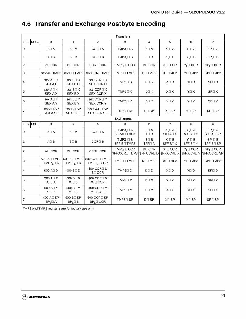
Core User Guide — S12CPU15UG V1.2
4.6 Transfer and Exchange Postbyte Encoding
Transfers
↓ LS MS→ 0 1 2 3 4 5 6 7
0 A⇒A B⇒A CCR⇒A TMP3L⇒A B⇒A XL⇒A YL⇒A SPL⇒A
1 A⇒B B⇒B CCR⇒B TMP3L⇒B B⇒B XL⇒B YL⇒B SPL⇒B
2 A⇒CCR B⇒CCR CCR⇒CCR TMP3L⇒CCR B⇒CCR XL⇒CCR YL⇒CCR SPL⇒CCR
3 sex:A⇒TMP2 sex:B⇒TMP2 sex:CCR⇒TMP2 TMP3⇒TMP2 D⇒TMP2 X⇒TMP2 Y⇒TMP2 SP⇒TMP2
4sex:A⇒DSEX A,D
sex:B⇒DSEX B,D
sex:CCR⇒DSEX CCR,D
TMP3⇒D D⇒D X⇒D Y⇒D SP⇒D
5sex:A⇒XSEX A,X
sex:B⇒XSEX B,X
sex:CCR⇒XSEX CCR,X
TMP3⇒X D⇒X X⇒X Y⇒X SP⇒X
6sex:A⇒YSEX A,Y
sex:B⇒YSEX B,Y
sex:CCR⇒YSEX CCR,Y
TMP3⇒Y D⇒Y X⇒Y Y⇒Y SP⇒Y
7sex:A⇒SPSEX A,SP
sex:B⇒SPSEX B,SP
sex:CCR⇒SPSEX CCR,SP
TMP3⇒SP D⇒SP X⇒SP Y⇒SP SP⇒SP
Exchanges
↓ LS MS→ 8 9 A B C D E F
0 A⇔A B⇔A CCR⇔ATMP3L⇒A
$00:A⇒TMP3B⇒AA⇒B
XL⇒A$00:A⇒X
YL⇒A$00:A⇒Y
SPL⇒A$00:A⇒SP
1 A⇔B B⇔B CCR⇔BTMP3L⇒B
$FF:B⇒TMP3B⇒B
$FF⇒AXL⇒B
$FF:B⇒XYL⇒B
$FF:B⇒YSPL⇒B
$FF:B⇒SP
2 A⇔CCR B⇔CCR CCR⇔CCRTMP3L⇒CCR
$FF:CCR⇒TMP3B⇒CCR
$FF:CCR⇒DXL⇒CCR
$FF:CCR⇒XYL⇒CCR
$FF:CCR⇒YSPL⇒CCR
$FF:CCR⇒SP
3$00:A⇒TMP2
TMP2L⇒A$00:B⇒TMP2
TMP2L⇒B$00:CCR⇒TMP2
TMP2L⇒CCRTMP3⇔TMP2 D⇔TMP2 X⇔TMP2 Y⇔TMP2 SP⇔TMP2
4 $00:A⇒D $00:B⇒D$00:CCR⇒D
B⇒CCRTMP3⇔D D⇔D X⇔D Y⇔D SP⇔D
5$00:A⇒X
XL⇒A$00:B⇒X
XL⇒B$00:CCR⇒X
XL⇒CCRTMP3⇔X D⇔X X⇔X Y⇔X SP⇔X
6$00:A⇒Y
YL⇒A$00:B⇒Y
YL⇒B$00:CCR⇒Y
YL⇒CCRTMP3⇔Y D⇔Y X⇔Y Y⇔Y SP⇔Y
7$00:A⇒SP
SPL⇒A$00:B⇒SP
SPL⇒B$00:CCR⇒SP
SPL⇒CCRTMP3⇔SP D⇔SP X⇔SP Y⇔SP SP⇔SP
TMP2 and TMP3 registers are for factory use only.
99
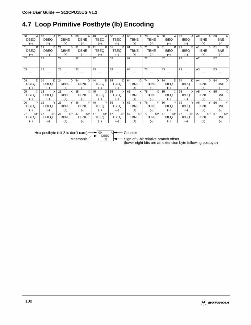
Core User Guide — S12CPU15UG V1.2
4.7 Loop Primitive Postbyte (lb) Encoding
00 ADBEQ
(+)
10 ADBEQ
(–)
20 ADBNE
(+)
30 ADBNE
(–)
40 ATBEQ
(+)
50 ATBEQ
(–)
60 ATBNE
(+)
70 ATBNE
(–)
80 AIBEQ
(+)
90 AIBEQ
(–)
A0 AIBNE
(+)
B0 AIBNE
(–)01 B
DBEQ(+)
11 BDBEQ
(–)
21 BDBNE
(+)
31 BDBNE
(–)
41 BTBEQ
(+)
51 BTBEQ
(–)
61 BTBNE
(+)
71 BTBNE
(–)
81 BIBEQ
(+)
91 BIBEQ
(–)
A1 BIBNE
(+)
B1 BIBNE
(–)02
—12
—22
—32
—42
—52
—62
—72
—82
—92
—A2
—B2
—
03—
13—
23—
33—
43—
53—
63—
73—
83—
93—
A3—
B3—
04 DDBEQ
(+)
14 DDBEQ
(–)
24 DDBNE
(+)
34 DDBNE
(–)
44 DTBEQ
(+)
54 DTBEQ
(–)
64 DTBNE
(+)
74 DTBNE
(–)
84 DIBEQ
(+)
94 DIBEQ
(–)
A4 DIBNE
(+)
B4 DIBNE
(–)05 X
DBEQ(+)
15 XDBEQ
(–)
25 XDBNE
(+)
35 XDBNE
(–)
45 XTBEQ
(+)
55 XTBEQ
(–)
65 XTBNE
(+)
75 XTBNE
(–)
85 XIBEQ
(+)
95 XIBEQ
(–)
A5 XIBNE
(+)
B5 XIBNE
(–)06 Y
DBEQ(+)
16 YDBEQ
(–)
26 YDBNE
(+)
36 YDBNE
(–)
46 YTBEQ
(+)
56 YTBEQ
(–)
66 YTBNE
(+)
76 YTBNE
(–)
86 YIBEQ
(+)
96 YIBEQ
(–)
A6 YIBNE
(+)
B6 YIBNE
(–)07 SP
DBEQ(+)
17 SPDBEQ
(–)
27 SPDBNE
(+)
37 SPDBNE
(–)
47 SPTBEQ
(+)
57 SPTBEQ
(–)
67 SPTBNE
(+)
77 SPTBNE
(–)
87 SPIBEQ
(+)
97 SPIBEQ
(–)
A7 SPIBNE
(+)
B7 SPIBNE
(–)
Hex postbyte (bit 3 is don’t care)
Mnemonic
Counter00DBEQ
(+)
A
Sign of 9-bit relative branch offset(lower eight bits are an extension byte following postbyte)
100
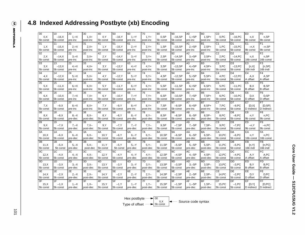
101
Core U
ser Guide —
S12C
PU
15UG
V1.2
0,PC const
D0–16,PC
5b const
E0n,X
9b const
F0n,SP
9b const
1,PC const
D1–15,PC
5b const
E1–n,X
9b const
F1–n,SP
9b const
2,PC const
D2–14,PC
5b const
E2n,X
16b const
F2n,SP
16b const
3,PC const
D3–13,PC
5b const
E3[n,X]
16b indr
F3[n,SP]
16b indr
4,PC const
D4–12,PC
5b const
E4A,X
A offset
F4A,SP
A offset
5,PC const
D5–11,PC
5b const
E5B,X
B offset
F5B,SP
B offset
6,PC const
D6–10,PC
5b const
E6D,X
D offset
F6D,SP
D offset
7,PC const
D7–9,PC
5b const
E7[D,X]
D indirect
F7[D,SP]
D indirect
8,PC const
D8–8,PC
5b const
E8n,Y
9b const
F8n,PC
9b const
9,PC const
D9–7,PC
5b const
E9–n,Y
9b const
F9–n,PC
9b const
10,PC const
DA–6,PC
5b const
EAn,Y
16b const
FAn,PC
16b const
11,PC const
DB–5,PC
5b const
EB[n,Y]
16b indr
FB[n,PC]
16b indr
12,PC const
DC–4,PC
5b const
ECA,Y
A offset
FCA,PC
A offset
13,PC const
DD–3,PC
5b const
EDB,Y
B offset
FDB,PC
B offset
14,PC const
DE–2,PC
5b const
EED,Y
D offset
FED,PC
D offset
15,PC const
DF–1,PC
5b const
EF[D,Y]
D indirect
FF[D,PC]
D indirect
4.8 Indexed Addressing Postbyte (xb) Encoding
000,X
5b const
10–16,X
5b const
201,+X
pre-inc
301,X+
post-inc
400,Y
5b const
50–16,Y
5b const
601,+Y
pre-inc
701,Y+
post-inc
800,SP
5b const
90–16,SP
5b const
A01,+SP
pre-inc
B01,SP+
post-inc
C0
5b01
1,X5b const
11–15,X
5b const
212,+X
pre-inc
312,X+
post-inc
411,Y
5b const
51–15,Y
5b const
612,+Y
pre-inc
712,Y+
post-inc
811,SP
5b const
91–15,SP
5b const
A12,+SP
pre-inc
B12,SP+
post-inc
C1
5b02
2,X5b const
12–14,X
5b const
223,+X
pre-inc
323,X+
post-inc
422,Y
5b const
52–14,Y
5b const
623,+Y
pre-inc
723,Y+
post-inc
822,SP
5b const
92–14,SP
5b const
A23,+SP
pre-inc
B23,SP+
post-inc
C2
5b03
3,X5b const
13–13,X
5b const
234,+X
pre-inc
334,X+
post-inc
433,Y
5b const
53–13,Y
5b const
634,+Y
pre-inc
734,Y+
post-inc
833,SP
5b const
93–13,SP
5b const
A34,+SP
pre-inc
B34,SP+
post-inc
C3
5b04
4,X5b const
14–12,X
5b const
245,+X
pre-inc
345,X+
post-inc
444,Y
5b const
54–12,Y
5b const
645,+Y
pre-inc
745,Y+
post-inc
844,SP
5b const
94–12,SP
5b const
A45,+SP
pre-inc
B45,SP+
post-inc
C4
5b05
5,X5b const
15–11,X
5b const
256,+X
pre-inc
356,X+
post-inc
455,Y
5b const
55–11,Y
5b const
656,+Y
pre-inc
756,Y+
post-inc
855,SP
5b const
95–11,SP
5b const
A56,+SP
pre-inc
B56,SP+
post-inc
C5
5b06
6,X5b const
16–10,X
5b const
267,+X
pre-inc
367,X+
post-inc
466,Y
5b const
56–10,Y
5b const
667,+Y
pre-inc
767,Y+
post-inc
866,SP
5b const
96–10,SP
5b const
A67,+SP
pre-inc
B67,SP+
post-inc
C6
5b07
7,X5b const
17–9,X
5b const
278,+X
pre-inc
378,X+
post-inc
477,Y
5b const
57–9,Y
5b const
678,+Y
pre-inc
778,Y+
post-inc
877,SP
5b const
97–9,SP
5b const
A78,+SP
pre-inc
B78,SP+
post-inc
C7
5b08
8,X5b const
18–8,X
5b const
288,–X
pre-dec
388,X–
post-dec
488,Y
5b const
58–8,Y
5b const
688,–Y
pre-dec
788,Y–
post-dec
888,SP
5b const
98–8,SP
5b const
A88,–SP
pre-dec
B88,SP–
post-dec
C8
5b09
9,X5b const
19–7,X
5b const
297,–X
pre-dec
397,X–
post-dec
499,Y
5b const
59–7,Y
5b const
697,–Y
pre-dec
797,Y–
post-dec
899,SP
5b const
99–7,SP
5b const
A97,–SP
pre-dec
B97,SP–
post-dec
C9
5b0A
10,X5b const
1A–6,X
5b const
2A6,–X
pre-dec
3A6,X–
post-dec
4A10,Y
5b const
5A–6,Y
5b const
6A6,–Y
pre-dec
7A6,Y–
post-dec
8A10,SP
5b const
9A–6,SP
5b const
AA6,–SP
pre-dec
BA6,SP–
post-dec
CA
5b0B
11,X5b const
1B–5,X
5b const
2B5,–X
pre-dec
3B5,X–
post-dec
4B11,Y
5b const
5B–5,Y
5b const
6B5,–Y
pre-dec
7B5,Y–
post-dec
8B11,SP
5b const
9B–5,SP
5b const
AB5,–SP
pre-dec
BB5,SP–
post-dec
CB
5b0C
12,X5b const
1C–4,X
5b const
2C4,–X
pre-dec
3C4,X–
post-dec
4C12,Y
5b const
5C–4,Y
5b const
6C4,–Y
pre-dec
7C4,Y–
post-dec
8C12,SP
5b const
9C–4,SP
5b const
AC4,–SP
pre-dec
BC4,SP–
post-dec
CC
5b0D
13,X5b const
1D–3,X
5b const
2D3,–X
pre-dec
3D3,X–
post-dec
4D13,Y
5b const
5D–3,Y
5b const
6D3,–Y
pre-dec
7D3,Y–
post-dec
8D13,SP
5b const
9D–3,SP
5b const
AD3,–SP
pre-dec
BD3,SP–
post-dec
CD
5b0E
14,X5b const
1E–2,X
5b const
2E2,–X
pre-dec
3E2,X–
post-dec
4E14,Y
5b const
5E–2,Y
5b const
6E2,–Y
pre-dec
7E2,Y–
post-dec
8E14,SP
5b const
9E–2,SP
5b const
AE2,–SP
pre-dec
BE2,SP–
post-dec
CE
5b0F
15,X5b const
1F–1,X
5b const
2F1,–X
pre-dec
3F1,X–
post-dec
4F15,Y
5b const
5F–1,Y
5b const
6F1,–Y
pre-dec
7F1,Y–
post-dec
8F15,SP
5b const
9F–1,SP
5b const
AF1,–SP
pre-dec
BF1,SP–
post-dec
CF
5b
Hex postbyte
Type of offsetSource code syntax
000,X
5b const

Core User Guide — S12CPU15UG V1.2
102
Core User Guide — S12CPU15UG V1.2
tion
lly
n at acking
roll outcation
ogramo belaced.tch. Ifycle.
data
re only
n of
aded with
Section 5 Instruction Execution
The CPU uses a three-stage instruction queue to facilitate instruction fetching and increase execuspeed. This section provides a general description of the instruction queue during normal programexecution and during changes in execution flow. Operation of the queue is automatic and generatransparent to the user.
5.1 Normal Instruction Execution
Queue logic prefetches program information and positions it for sequential execution, one instructiotime. The relationship between bus cycles and execution cycles is straightforward and facilitates traand debugging.
There are three 16-bit stages in the instruction queue. Instructions enter the queue at stage1 andafter stage 3. Each byte in the queue is selectable. An opcode-prediction algorithm determines the loof the next opcode in the instruction queue.
Each instruction refills the queue by fetching the same number of bytes that the instruction uses. Prinformation is fetched in aligned 16-bit words. Each program fetch indicates that two bytes need treplaced in the instruction queue. Each optional fetch indicates that only one byte needs to be repFor example, an instruction composed of five bytes does two program fetches and one optional fethe first byte of the five-byte instruction was even-aligned, the optional fetch is converted into a free cIf the first byte was odd-aligned, the optional fetch is executed as a program fetch.
Two external pins, IPIPE[1:0], provide time-multiplexed information about instruction execution andmovement in the queue. Decoding and using the IPIPE signals is discussed in.
5.2 Execution Sequence
All queue operations are defined by two basic queue movement cycles. Queue movement cycles aone factor in instruction execution time and should not be confused with bus cycles.
5.2.1 No Movement
There is no data movement in the instruction queue during the cycle. This occurs during executioinstructions that must perform a number of internal operations, such as division instructions.
5.2.2 Advance and Load from Data Bus
The content of queue stage 1 advances to stage 2, stage 2 advances to stage 3, and stage 1 is loa word of program information from the data bus.
103
Core User Guide — S12CPU15UG V1.2
cles.e
tion, X
ns aressing
can usethree
RTS).e queue.
00 to therites ahree
erefill the
affectitive
5.3 Changes of Flow
Most of the time, the instruction queue operates in a continuous sequence of queue movement cyWhen program flow changes because of an exception, subroutine call, branch, or jump, the queuautomatically adjusts its movement sequence to accommodate the change in program flow.
5.3.1 Exceptions
Exceptions include three types of reset, an unimplemented opcode trap, a software interrupt instrucbit maskable interrupts, and I bit maskable interrupts.
To minimize the effect of queue operation on exception handling:
• The exception vector fetch is the first part of exception processing.
• Fetches to refill the queue from the new address are interleaved with the context-stackingoperations, so that program access time does not delay the switch.
Please seeSection 6 of this guide for more detailed information on exception processing.
5.3.2 Subroutines
The CPU can branch to (BSR), jump to (JSR), or CALL subroutines. The BSR and JSR instructiofor accessing subroutines in the normal 64K byte address space. The CALL instruction is for accesubroutines in expanded memory.
BSR uses relative addressing mode to generate the effective address of the subroutine, while JSRother addressing modes. Both instructions calculate a return address, stack the address, then do program word fetches to refill the queue.
A subroutine in the normal 64K byte address space ends with a return from subroutine instruction (RTS unstacks the return address and does three program word fetches from that address to refill th
CALL is similar to JSR. MCUs with expanded memory treat the 16K bytes of addresses from $80$BFFF as an expanded memory window. An 8-bit PPAGE register switches the memory pages inwindow. CALL calculates and stacks a return address along with the current PPAGE value and wnew instruction-supplied value to PPAGE. Then it calculates the subroutine address and fetches tprogram words from that address to refill the queue.
A subroutine in expanded memory ends with a return from call instruction (RTC). RTC unstacks thPPAGE value and the return address and does three program word fetches from that address to queue.
5.3.3 Branches
A branch instruction changes the execution flow when a specific condition exists. There are shortconditional branches, long conditional branches, and bit-condition branches. All branch instructionsthe queue similarly, but there are differences in cycle counts between the various types. Loop priminstructions are a special type of branch instruction for implementing counter-based loops.
104
Core User Guide — S12CPU15UG V1.2
of flow
wordm word,
egin atffset inord
equirese.
of thet in thetcle.
umber
a freenext
relativeer and
n arequireh theTo case.ing toing to
A branch instruction has two execution cases. Either the branch condition is satisfied, and a changetakes place, or the condition is not satisfied, and no change of flow occurs.
5.3.3.1 Short Branches
The branch-not-taken case for a short branch is simple. Since the instruction consists of a single containing both an opcode and an 8-bit offset, the queue advances, the CPU fetches another prograand execution continues with the next instruction.
The branch-taken case for a short branch requires that the queue be refilled so that execution can ba new address. First, the CPU calculates the effective address of the destination using the relative othe instruction. Then it loads the address into the program counter, and performs three program wfetches at the new address to refill the queue.
5.3.3.2 Long Branches
The branch-not-taken case for a long branch requires three cycles, while the branch-taken case rfour cycles. This is due to differences in the amount of program information needed to fill the queu
A long branch instruction begins with a $18 prebyte which indicates that the opcode is on page 2 opcode map. The CPU treats the prebyte as a special one-byte instruction. To maintain alignmentwo-byte queue, the first cycle of a long branch instruction is an optional cycle. If the prebyte is noaligned, the CPU does a program word access; if the prebyte is aligned, the first cycle is a free cy
Optional cycles align byte-sized and misaligned instructions with aligned word-length instructions.Program information is always fetched as aligned 16-bit words. When an instruction has an odd nof bytes, and the first byte is not aligned with an even byte boundary, the optional cycle makes anadditional program word access that maintains queue order. In all other cases, the optional cycle iscycle. In the branch-not-taken case, the queue advances so that execution can continue with the instruction. The CPU does one program fetch and one optional fetch to refill the queue.
In the branch-taken case, the CPU calculates the effective address of the branch using the 16-bitoffset contained in the second word of the instruction. It loads the address into the program countthen does three program word fetches at the new address to refill the queue.
5.3.3.3 Bit Condition Branches
A bit-condition branch instruction reads a location in memory and branches if the bits in that locatioin a certain state. It can use direct, extended, or indexed addressing mode. Indexed operations revarying amounts of information to determine the effective address, so instruction length varies witaddressing mode. The amount of program information fetched also varies with instruction length. shorten execution time, the CPU does one program word fetch in anticipation of the branch-takenThe data from this fetch is ignored if the branch is not taken, and the CPU refills the queue accordthe instruction length. If the branch is taken, the CPU refills the queue from the new address accordthe instruction length.
105

Core User Guide — S12CPU15UG V1.2
met,re are
tn. To case.nd oneal
exedlengthctiondress.
ed ofmplyampleany
w
5.3.3.4 Loop Primitive Instructions
A loop primitive instruction tests a counter value in a register or accumulator. If the test condition isthe CPU branches to an address specified by a 9-bit relative offset contained in the instruction. Theautoincrement and autodecrement versions of the instructions. The test and increment/decremenoperations are performed on internal CPU registers, and require no additional program informatioshorten execution time, the CPU does one program word fetch in anticipation of the branch-takenThe data from this fetch is ignored if the branch is not taken, and the CPU does one program fetch aoptional fetch to refill the queue. If the branch is taken, the CPU refills the queue with two additionprogram word fetches at the new address.
5.3.4 Jumps
JMP is the simplest change-of-flow instruction. JMP can use extended or indexed addressing. Indoperations require varying amounts of information to determine the effective address, so instructionvaries with the addressing mode. The amount of program information fetched also varies with instrulength. In all forms of JMP, the CPU refills the queue with three program word fetches at the new ad
5.4 Instruction Timing
TheAccess Detailcolumn of the summary inTable 5-1 shows how many bytes of information the CPUaccesses while executing an instruction. With this information and knowledge of the type and spememory in the system, you can determine the execution time for any instruction in any system. Sicount the code letters to determine the execution time of an instruction in a best-case system. An exof a best-case system is a single-chip 16-bit system with no 16-bit off-boundary data accesses to locations other than on-chip RAM.
A description of the notation used in each column of the table is given in the subsections that folloincluding that of theAccess Detail column. This information as well as the summary inTable 5-1 isrepeated fromSection 1 of this guide for completeness.
Table 5-1 Instruction Set Summary
Source Form Operation AddressMode
MachineCoding (Hex) Access Detail S X H I N Z V C
ABA Add B to A; (A)+(B)⇒A INH 18 06 OO
ABXSame as LEAX B,X Add B to X; (X)+(B)⇒X IDX 1A E5 Pf
ABYSame as LEAY B,Y Add B to Y; (Y)+(B)⇒Y IDX 19 ED Pf
ADCA #opr8iADCA opr8aADCA opr16aADCA oprx0_xysppcADCA oprx9,xysppcADCA oprx16,xysppcADCA [D,xysppc]ADCA [oprx16,xysppc]
Add with carry to A; (A)+(M)+C⇒Aor (A)+imm+C⇒A
IMMDIREXTIDXIDX1IDX2[D,IDX][IDX2]
89 ii99 ddB9 hh llA9 xbA9 xb ffA9 xb ee ffA9 xbA9 xb ee ff
PrPfrPOrPfrPOfrPPfIfrPffIPrPf
– – ∆ – ∆ ∆ ∆ ∆
– – – – – – – –
– – – – – – – –
– – ∆ – ∆ ∆ ∆ ∆
106
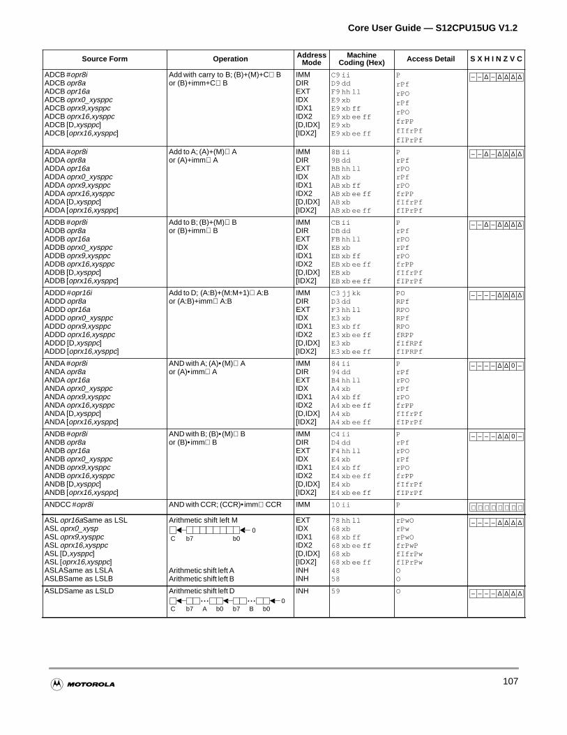
Core User Guide — S12CPU15UG V1.2
ADCB #opr8iADCB opr8aADCB opr16aADCB oprx0_xysppcADCB oprx9,xysppcADCB oprx16,xysppcADCB [D,xysppc]ADCB [oprx16,xysppc]
Add with carry to B; (B)+(M)+C⇒Bor (B)+imm+C⇒B
IMMDIREXTIDXIDX1IDX2[D,IDX][IDX2]
C9 iiD9 ddF9 hh llE9 xbE9 xb ffE9 xb ee ffE9 xbE9 xb ee ff
PrPfrPOrPfrPOfrPPfIfrPffIPrPf
ADDA #opr8iADDA opr8aADDA opr16aADDA oprx0_xysppcADDA oprx9,xysppcADDA oprx16,xysppcADDA [D,xysppc]ADDA [oprx16,xysppc]
Add to A; (A)+(M)⇒Aor (A)+imm⇒A
IMMDIREXTIDXIDX1IDX2[D,IDX][IDX2]
8B ii9B ddBB hh llAB xbAB xb ffAB xb ee ffAB xbAB xb ee ff
PrPfrPOrPfrPOfrPPfIfrPffIPrPf
ADDB #opr8iADDB opr8aADDB opr16aADDB oprx0_xysppcADDB oprx9,xysppcADDB oprx16,xysppcADDB [D,xysppc]ADDB [oprx16,xysppc]
Add to B; (B)+(M)⇒Bor (B)+imm⇒B
IMMDIREXTIDXIDX1IDX2[D,IDX][IDX2]
CB iiDB ddFB hh llEB xbEB xb ffEB xb ee ffEB xbEB xb ee ff
PrPfrPOrPfrPOfrPPfIfrPffIPrPf
ADDD #opr16iADDD opr8aADDD opr16aADDD oprx0_xysppcADDD oprx9,xysppcADDD oprx16,xysppcADDD [D,xysppc]ADDD [oprx16,xysppc]
Add to D; (A:B)+(M:M+1)⇒A:Bor (A:B)+imm⇒A:B
IMMDIREXTIDXIDX1IDX2[D,IDX][IDX2]
C3 jj kkD3 ddF3 hh llE3 xbE3 xb ffE3 xb ee ffE3 xbE3 xb ee ff
PORPfRPORPfRPOfRPPfIfRPffIPRPf
ANDA #opr8iANDA opr8aANDA opr16aANDA oprx0_xysppcANDA oprx9,xysppcANDA oprx16,xysppcANDA [D,xysppc]ANDA [oprx16,xysppc]
AND with A; (A)•(M)⇒Aor (A)•imm⇒A
IMMDIREXTIDXIDX1IDX2[D,IDX][IDX2]
84 ii94 ddB4 hh llA4 xbA4 xb ffA4 xb ee ffA4 xbA4 xb ee ff
PrPfrPOrPfrPOfrPPfIfrPffIPrPf
ANDB #opr8iANDB opr8aANDB opr16aANDB oprx0_xysppcANDB oprx9,xysppcANDB oprx16,xysppcANDB [D,xysppc]ANDB [oprx16,xysppc]
AND with B; (B)•(M)⇒Bor (B)•imm⇒B
IMMDIREXTIDXIDX1IDX2[D,IDX][IDX2]
C4 iiD4 ddF4 hh llE4 xbE4 xb ffE4 xb ee ffE4 xbE4 xb ee ff
PrPfrPOrPfrPOfrPPfIfrPffIPrPf
ANDCC #opr8i AND with CCR; (CCR)•imm⇒CCR IMM 10 ii P
ASL opr16aSame as LSLASL oprx0_xyspASL oprx9,xysppcASL oprx16,xysppcASL [D,xysppc]ASL [oprx16,xysppc]ASLASame as LSLAASLBSame as LSLB
Arithmetic shift left M
Arithmetic shift left AArithmetic shift left B
EXTIDXIDX1IDX2[D,IDX][IDX2]INHINH
78 hh ll68 xb68 xb ff68 xb ee ff68 xb68 xb ee ff4858
rPwOrPwrPwOfrPwPfIfrPwfIPrPwOO
ASLDSame as LSLD Arithmetic shift left D INH 59 O
Source Form Operation AddressMode
MachineCoding (Hex) Access Detail S X H I N Z V C
– – ∆ – ∆ ∆ ∆ ∆
– – ∆ – ∆ ∆ ∆ ∆
– – ∆ – ∆ ∆ ∆ ∆
– – – – ∆ ∆ ∆ ∆
– – – – ∆ ∆ 0 –
– – – – ∆ ∆ 0 –
⇓ ⇓ ⇓ ⇓ ⇓ ⇓ ⇓ ⇓
C0
b7 b0
– – – – ∆ ∆ ∆ ∆
• • • • • •
C0
b7 b0A Bb7b0
– – – – ∆ ∆ ∆ ∆
107
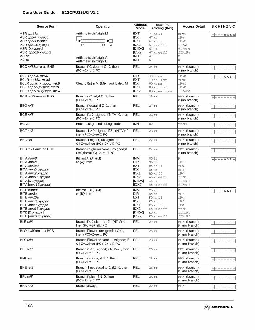
Core User Guide — S12CPU15UG V1.2
ASR opr16aASR oprx0_xysppcASR oprx9,xysppcASR oprx16,xysppcASR [D,xysppc]ASR [oprx16,xysppc]ASRAASRB
Arithmetic shift right M
Arithmetic shift right AArithmetic shift right B
EXTIDXIDX1IDX2[D,IDX][IDX2]INHINH
77 hh ll67 xb67 xb ff67 xb ee ff67 xb67 xb ee ff4757
rPwOrPwrPwOfrPwPfIfrPwfIPrPwOO
BCC rel8Same as BHS Branch if C clear; if C=0, then(PC)+2+rel⇒PC
REL 24 rr PPP (branch)P (no branch)
BCLR opr8a, msk8BCLR opr16a, msk8BCLR oprx0_xysppc, msk8BCLR oprx9,xysppc, msk8BCLR oprx16,xysppc, msk8
Clear bit(s) in M; (M)•mask byte⇒M
DIREXTIDXIDX1IDX2
4D dd mm1D hh ll mm0D xb mm0D xb ff mm0D xb ee ff mm
rPwOrPwPrPwOrPwPfrPwPO
BCS rel8Same as BLO Branch if C set; if C=1, then(PC)+2+rel⇒PC
REL 25 rr PPP (branch)P (no branch)
BEQ rel8 Branch if equal; if Z=1, then(PC)+2+rel⇒PC
REL 27 rr PPP (branch)P (no branch)
BGE rel8 Branch if ≥ 0, signed; if N⊕V=0, then(PC)+2+rel⇒PC
REL 2C rr PPP (branch)P (no branch)
BGND Enter background debug mode INH 00 VfPPP
BGT rel8 Branch if > 0, signed; if Z | (N⊕V)=0,then (PC)+2+rel⇒PC
REL 2E rr PPP (branch)P (no branch)
BHI rel8 Branch if higher, unsigned; ifC | Z=0, then (PC)+2+rel⇒PC
REL 22 rr PPP (branch)P (no branch)
BHS rel8Same as BCC Branchifhigherorsame,unsigned;ifC=0,then(PC)+2+rel⇒PC
REL 24 rr PPP (branch)P (no branch)
BITA #opr8iBITA opr8aBITA opr16aBITA oprx0_xysppcBITA oprx9,xysppcBITA oprx16,xysppcBITA [D,xysppc]BITA [oprx16,xysppc]
Bit test A; (A)•(M)or (A)•imm
IMMDIREXTIDXIDX1IDX2[D,IDX][IDX2]
85 ii95 ddB5 hh llA5 xbA5 xb ffA5 xb ee ffA5 xbA5 xb ee ff
PrPfrPOrPfrPOfrPPfIfrPffIPrPf
BITB #opr8iBITB opr8aBITB opr16aBITB oprx0_xysppcBITB oprx9,xysppcBITB oprx16,xysppcBITB [D,xysppc]BITB [oprx16,xysppc]
Bit test B; (B)•(M)or (B)•imm
IMMDIREXTIDXIDX1IDX2[D,IDX][IDX2]
C5 iiD5 ddF5 hh llE5 xbE5 xb ffE5 xb ee ffE5 xbE5 xb ee ff
PrPfrPOrPfrPOfrPPfIfrPffIPrPf
BLE rel8 Branch if≤ 0,signed; ifZ | (N⊕V)=1,then(PC)+2+rel⇒PC
REL 2F rr PPP (branch)P (no branch)
BLO rel8Same as BCS Branch if lower, unsigned; if C=1,then (PC)+2+rel⇒PC
REL 25 rr PPP (branch)P (no branch)
BLS rel8 Branch if lower or same, unsigned; ifC | Z=1, then (PC)+2+rel⇒PC
REL 23 rr PPP (branch)P (no branch)
BLT rel8 Branch if < 0, signed; if N⊕V=1, then(PC)+2+rel⇒PC
REL 2D rr PPP (branch)P (no branch)
BMI rel8 Branch if minus; if N=1, then(PC)+2+rel⇒PC
REL 2B rr PPP (branch)P (no branch)
BNE rel8 Branch if not equal to 0; if Z=0, then(PC)+2+rel⇒PC
REL 26 rr PPP (branch)P (no branch)
BPL rel8 Branch if plus; if N=0, then(PC)+2+rel⇒PC
REL 2A rr PPP (branch)P (no branch)
BRA rel8 Branch always REL 20 rr PPP
Source Form Operation AddressMode
MachineCoding (Hex) Access Detail S X H I N Z V C
Cb7 b0
– – – – ∆ ∆ ∆ ∆
– – – – – – – –
– – – – ∆ ∆ 0 –
– – – – – – – –
– – – – – – – –
– – – – – – – –
– – – – – – – –
– – – – – – – –
– – – – – – – –
– – – – – – – –
– – – – ∆ ∆ 0 –
– – – – ∆ ∆ 0 –
– – – – – – – –
– – – – – – – –
– – – – – – – –
– – – – – – – –
– – – – – – – –
– – – – – – – –
– – – – – – – –
– – – – – – – –
108
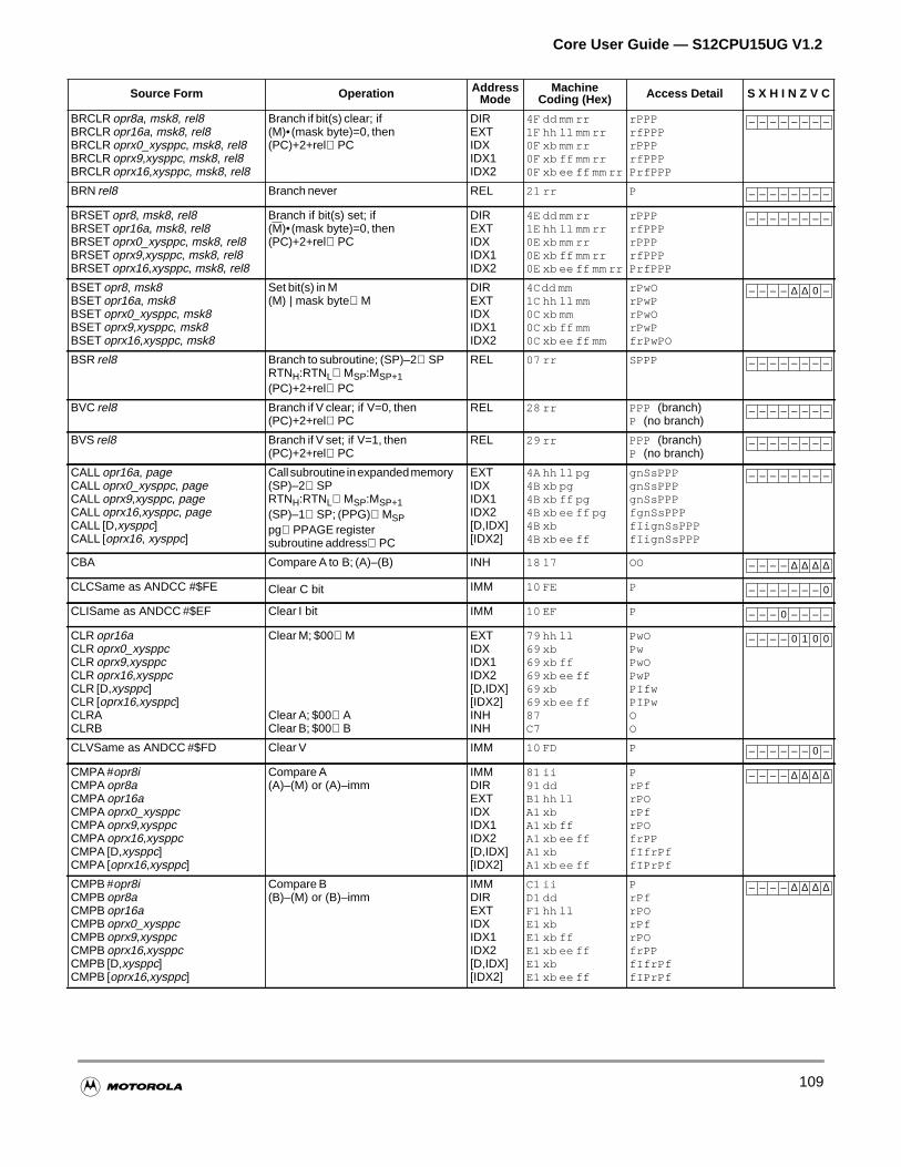
Core User Guide — S12CPU15UG V1.2
BRCLR opr8a, msk8, rel8BRCLR opr16a, msk8, rel8BRCLR oprx0_xysppc, msk8, rel8BRCLR oprx9,xysppc, msk8, rel8BRCLR oprx16,xysppc, msk8, rel8
Branch if bit(s) clear; if(M)•(mask byte)=0, then(PC)+2+rel⇒PC
DIREXTIDXIDX1IDX2
4F dd mm rr1F hh ll mm rr0F xb mm rr0F xb ff mm rr0F xb ee ff mm rr
rPPPrfPPPrPPPrfPPPPrfPPP
BRN rel8 Branch never REL 21 rr P
BRSET opr8, msk8, rel8BRSET opr16a, msk8, rel8BRSET oprx0_xysppc, msk8, rel8BRSET oprx9,xysppc, msk8, rel8BRSET oprx16,xysppc, msk8, rel8
Branch if bit(s) set; if(M)•(mask byte)=0, then(PC)+2+rel⇒PC
DIREXTIDXIDX1IDX2
4E dd mm rr1E hh ll mm rr0E xb mm rr0E xb ff mm rr0E xb ee ff mm rr
rPPPrfPPPrPPPrfPPPPrfPPP
BSET opr8, msk8BSET opr16a, msk8BSET oprx0_xysppc, msk8BSET oprx9,xysppc, msk8BSET oprx16,xysppc, msk8
Set bit(s) in M(M) | mask byte⇒M
DIREXTIDXIDX1IDX2
4Cdd mm1C hh ll mm0C xb mm0C xb ff mm0C xb ee ff mm
rPwOrPwPrPwOrPwPfrPwPO
BSR rel8 Branch to subroutine; (SP)–2⇒SPRTNH:RTNL⇒MSP:MSP+1(PC)+2+rel⇒PC
REL 07 rr SPPP
BVC rel8 Branch if V clear; if V=0, then(PC)+2+rel⇒PC
REL 28 rr PPP (branch)P (no branch)
BVS rel8 Branch if V set; if V=1, then(PC)+2+rel⇒PC
REL 29 rr PPP (branch)P (no branch)
CALL opr16a, pageCALL oprx0_xysppc, pageCALL oprx9,xysppc, pageCALL oprx16,xysppc, pageCALL [D,xysppc]CALL [oprx16, xysppc]
Call subroutine inexpandedmemory(SP)–2⇒SPRTNH:RTNL⇒MSP:MSP+1(SP)–1⇒SP; (PPG)⇒MSPpg⇒PPAGE registersubroutine address⇒PC
EXTIDXIDX1IDX2[D,IDX][IDX2]
4A hh ll pg4B xb pg4B xb ff pg4B xb ee ff pg4B xb4B xb ee ff
gnSsPPPgnSsPPPgnSsPPPfgnSsPPPfIignSsPPPfIignSsPPP
CBA Compare A to B; (A)–(B) INH 18 17 OO
CLCSame as ANDCC #$FE Clear C bit IMM 10 FE P
CLISame as ANDCC #$EF Clear I bit IMM 10 EF P
CLR opr16aCLR oprx0_xysppcCLR oprx9,xysppcCLR oprx16,xysppcCLR [D,xysppc]CLR [oprx16,xysppc]CLRACLRB
Clear M; $00⇒M
Clear A; $00⇒AClear B; $00⇒B
EXTIDXIDX1IDX2[D,IDX][IDX2]INHINH
79 hh ll69 xb69 xb ff69 xb ee ff69 xb69 xb ee ff87C7
PwOPwPwOPwPPIfwPIPwOO
CLVSame as ANDCC #$FD Clear V IMM 10 FD P
CMPA #opr8iCMPA opr8aCMPA opr16aCMPA oprx0_xysppcCMPA oprx9,xysppcCMPA oprx16,xysppcCMPA [D,xysppc]CMPA [oprx16,xysppc]
Compare A(A)–(M) or (A)–imm
IMMDIREXTIDXIDX1IDX2[D,IDX][IDX2]
81 ii91 ddB1 hh llA1 xbA1 xb ffA1 xb ee ffA1 xbA1 xb ee ff
PrPfrPOrPfrPOfrPPfIfrPffIPrPf
CMPB #opr8iCMPB opr8aCMPB opr16aCMPB oprx0_xysppcCMPB oprx9,xysppcCMPB oprx16,xysppcCMPB [D,xysppc]CMPB [oprx16,xysppc]
Compare B(B)–(M) or (B)–imm
IMMDIREXTIDXIDX1IDX2[D,IDX][IDX2]
C1 iiD1 ddF1 hh llE1 xbE1 xb ffE1 xb ee ffE1 xbE1 xb ee ff
PrPfrPOrPfrPOfrPPfIfrPffIPrPf
Source Form Operation AddressMode
MachineCoding (Hex) Access Detail S X H I N Z V C
– – – – – – – –
– – – – – – – –
– – – – – – – –
– – – – ∆ ∆ 0 –
– – – – – – – –
– – – – – – – –
– – – – – – – –
– – – – – – – –
– – – – ∆ ∆ ∆ ∆
– – – – – – – 0
– – – 0 – – – –
– – – – 0 1 0 0
– – – – – – 0 –
– – – – ∆ ∆ ∆ ∆
– – – – ∆ ∆ ∆ ∆
109
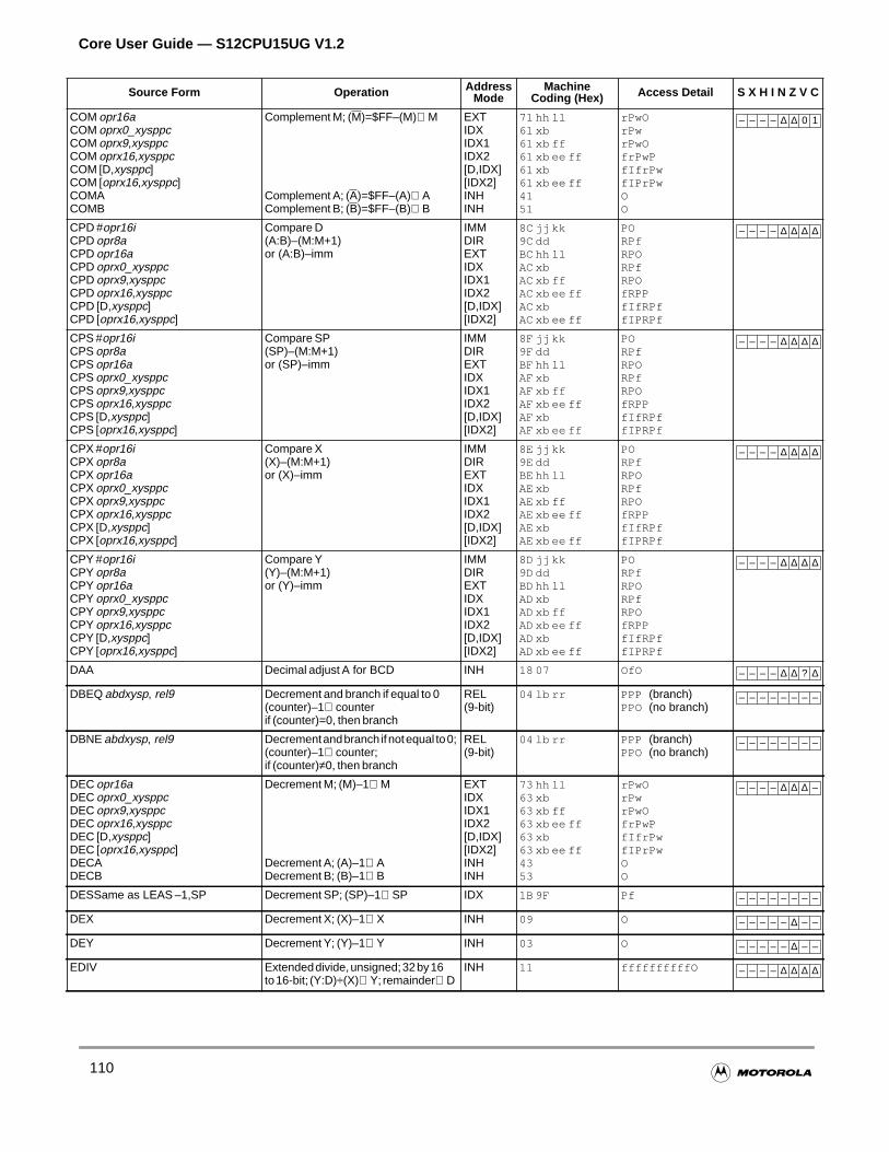
Core User Guide — S12CPU15UG V1.2
COM opr16aCOM oprx0_xysppcCOM oprx9,xysppcCOM oprx16,xysppcCOM [D,xysppc]COM [oprx16,xysppc]COMACOMB
Complement M; (M)=$FF–(M)⇒M
Complement A; (A)=$FF–(A)⇒AComplement B; (B)=$FF–(B)⇒B
EXTIDXIDX1IDX2[D,IDX][IDX2]INHINH
71 hh ll61 xb61 xb ff61 xb ee ff61 xb61 xb ee ff4151
rPwOrPwrPwOfrPwPfIfrPwfIPrPwOO
CPD #opr16iCPD opr8aCPD opr16aCPD oprx0_xysppcCPD oprx9,xysppcCPD oprx16,xysppcCPD [D,xysppc]CPD [oprx16,xysppc]
Compare D(A:B)–(M:M+1)or (A:B)–imm
IMMDIREXTIDXIDX1IDX2[D,IDX][IDX2]
8C jj kk9C ddBC hh llAC xbAC xb ffAC xb ee ffAC xbAC xb ee ff
PORPfRPORPfRPOfRPPfIfRPffIPRPf
CPS #opr16iCPS opr8aCPS opr16aCPS oprx0_xysppcCPS oprx9,xysppcCPS oprx16,xysppcCPS [D,xysppc]CPS [oprx16,xysppc]
Compare SP(SP)–(M:M+1)or (SP)–imm
IMMDIREXTIDXIDX1IDX2[D,IDX][IDX2]
8F jj kk9F ddBF hh llAF xbAF xb ffAF xb ee ffAF xbAF xb ee ff
PORPfRPORPfRPOfRPPfIfRPffIPRPf
CPX #opr16iCPX opr8aCPX opr16aCPX oprx0_xysppcCPX oprx9,xysppcCPX oprx16,xysppcCPX [D,xysppc]CPX [oprx16,xysppc]
Compare X(X)–(M:M+1)or (X)–imm
IMMDIREXTIDXIDX1IDX2[D,IDX][IDX2]
8E jj kk9E ddBE hh llAE xbAE xb ffAE xb ee ffAE xbAE xb ee ff
PORPfRPORPfRPOfRPPfIfRPffIPRPf
CPY #opr16iCPY opr8aCPY opr16aCPY oprx0_xysppcCPY oprx9,xysppcCPY oprx16,xysppcCPY [D,xysppc]CPY [oprx16,xysppc]
Compare Y(Y)–(M:M+1)or (Y)–imm
IMMDIREXTIDXIDX1IDX2[D,IDX][IDX2]
8D jj kk9D ddBD hh llAD xbAD xb ffAD xb ee ffAD xbAD xb ee ff
PORPfRPORPfRPOfRPPfIfRPffIPRPf
DAA Decimal adjust A for BCD INH 18 07 OfO
DBEQ abdxysp, rel9 Decrement and branch if equal to 0(counter)–1⇒counterif (counter)=0, then branch
REL(9-bit)
04 lb rr PPP (branch)PPO (no branch)
DBNE abdxysp, rel9 Decrementandbranch ifnotequal to0;(counter)–1⇒counter;if (counter)≠0, then branch
REL(9-bit)
04 lb rr PPP (branch)PPO (no branch)
DEC opr16aDEC oprx0_xysppcDEC oprx9,xysppcDEC oprx16,xysppcDEC [D,xysppc]DEC [oprx16,xysppc]DECADECB
Decrement M; (M)–1⇒M
Decrement A; (A)–1⇒ADecrement B; (B)–1⇒B
EXTIDXIDX1IDX2[D,IDX][IDX2]INHINH
73 hh ll63 xb63 xb ff63 xb ee ff63 xb63 xb ee ff4353
rPwOrPwrPwOfrPwPfIfrPwfIPrPwOO
DESSame as LEAS –1,SP Decrement SP; (SP)–1⇒SP IDX 1B 9F Pf
DEX Decrement X; (X)–1⇒X INH 09 O
DEY Decrement Y; (Y)–1⇒Y INH 03 O
EDIV Extendeddivide,unsigned;32by16to16-bit; (Y:D)÷(X)⇒Y; remainder⇒D
INH 11 ffffffffffO
Source Form Operation AddressMode
MachineCoding (Hex) Access Detail S X H I N Z V C
– – – – ∆ ∆ 0 1
– – – – ∆ ∆ ∆ ∆
– – – – ∆ ∆ ∆ ∆
– – – – ∆ ∆ ∆ ∆
– – – – ∆ ∆ ∆ ∆
– – – – ∆ ∆ ? ∆
– – – – – – – –
– – – – – – – –
– – – – ∆ ∆ ∆ –
– – – – – – – –
– – – – – ∆ – –
– – – – – ∆ – –
– – – – ∆ ∆ ∆ ∆
110
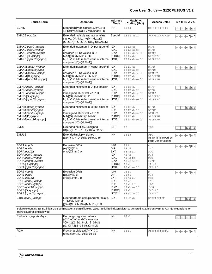
Core User Guide — S12CPU15UG V1.2
EDIVS Extendeddivide,signed;32by16 to16-bit; (Y:D)÷(X)⇒Yremainder⇒D
INH 18 14 OffffffffffO
EMACS opr16a Extended multiply and accumulate,signed; (MX:MX+1)×(MY:MY+1)+(M~M+3)⇒M~M+3; 16 by 16 to 32-bit
Special 18 12 hh ll ORROfffRRfWWP
EMAXD oprx0_xysppcEMAXD oprx9,xysppcEMAXD oprx16,xysppcEMAXD [D,xysppc]EMAXD [oprx16,xysppc]
Extended maximum in D; put larger of2unsigned 16-bit values in DMAX[(D), (M:M+1)]⇒DN, Z, V, C bits reflect result of internalcompare [(D)–(M:M+1)]
IDXIDX1IDX2[D,IDX][IDX2]
18 1A xb18 1A xb ff18 1A xb ee ff18 1A xb18 1A xb ee ff
ORPfORPOOfRPPOfIfRPfOfIPRPf
EMAXM oprx0_xysppcEMAXM oprx9,xysppcEMAXM oprx16,xysppcEMAXM [D,xysppc]EMAXM [oprx16,xysppc]
Extended maximum in M; put larger of2unsigned 16-bit values in MMAX[(D), (M:M+1)]⇒M:M+1N, Z, V, C bits reflect result of internalcompare [(D)–(M:M+1)]
IDXIDX1IDX2[D,IDX][IDX2]
18 1E xb18 1E xb ff18 1E xb ee ff18 1E xb18 1E xb ee ff
ORPWORPWOOfRPWPOfIfRPWOfIPRPW
EMIND oprx0_xysppcEMIND oprx9,xysppcEMIND oprx16,xysppcEMIND [D,xysppc]EMIND [oprx16,xysppc]
Extended minimum in D; put smallerof2 unsigned 16-bit values in DMIN[(D), (M:M+1)]⇒DN, Z, V, C bits reflect result of internalcompare [(D)–(M:M+1)]
IDXIDX1IDX2[D,IDX][IDX2]
18 1B xb18 1B xb ff18 1B xb ee ff18 1B xb18 1B xb ee ff
ORPfORPOOfRPPOfIfRPfOfIPRPf
EMINM oprx0_xysppcEMINM oprx9,xysppcEMINM oprx16,xysppcEMINM [D,xysppc]EMINM [oprx16,xysppc]
Extended minimum in M; put smallerof2 unsigned 16-bit values in MMIN[(D), (M:M+1)]⇒M:M+1N, Z, V, C bits reflect result of internalcompare [(D)–(M:M+1)]
IDXIDX1IDX2[D,IDX][IDX2]
18 1F xb18 1F xb ff18 1F xb ee ff18 1F xb18 1F xb ee ff
ORPWORPWOOfRPWPOfIfRPWOfIPRPW
EMUL Extended multiply, unsigned(D)×(Y)⇒Y:D; 16 by 16 to 32-bit
INH 13 ffO
EMULS Extended multiply, signed(D)×(Y)⇒Y:D; 16 by 16 to 32-bit
INH 18 13 OfOOffO (if followed bypage 2 instruction)
EORA #opr8iEORA opr8aEORA opr16aEORA oprx0_xysppcEORA oprx9,xysppcEORA oprx16,xysppcEORA [D,xysppc]EORA [oprx16,xysppc]
Exclusive OR A(A)⊕(M)⇒Aor (A)⊕imm⇒A
IMMDIREXTIDXIDX1IDX2[D,IDX][IDX2]
88 ii98 ddB8 hh llA8 xbA8 xb ffA8 xb ee ffA8 xbA8 xb ee ff
PrPfrPOrPfrPOfrPPfIfrPffIPrPf
EORB #opr8iEORB opr8aEORB opr16aEORB oprx0_xysppcEORB oprx9,xysppcEORB oprx16,xysppcEORB [D,xysppc]EORB [oprx16,xysppc]
Exclusive OR B(B)⊕(M)⇒Bor (B)⊕imm⇒B
IMMDIREXTIDXIDX1IDX2[D,IDX][IDX2]
C8 iiD8 ddF8 hh llE8 xbE8 xb ffE8 xb ee ffE8 xbE8 xb ee ff
PrPfrPOrPfrPOfrPPfIfrPffIPrPf
ETBL oprx0_xysppc Extended table lookupand interpolate,16-bit; (M:M+1)+[(B)×((M+2:M+3)–(M:M+1))]⇒D
IDX 18 3F xb ORRffffffP
Before executing ETBL, initialize B with fractional part of lookup value; initialize index register to point to first table entry (M:M+1). No extensions orindirect addressing allowed.
EXG abcdxysp,abcdxysp Exchangeregistercontents(r1)⇔(r2) r1 and r2 same size$00:(r1)⇒r2r1=8-bit; r2=16-bit(r1L)⇔(r2)r1=16-bit; r2=8-bit
INH B7 eb P
FDIV Fractional divide; (D)÷(X)⇒Xremainder⇒D; 16 by 16-bit
INH 18 11 OffffffffffO
Source Form Operation AddressMode
MachineCoding (Hex) Access Detail S X H I N Z V C
– – – – ∆ ∆ ∆ ∆
– – – – ∆ ∆ ∆ ∆
– – – – ∆ ∆ ∆ ∆
– – – – ∆ ∆ ∆ ∆
– – – – ∆ ∆ ∆ ∆
– – – – ∆ ∆ ∆ ∆
– – – – ∆ ∆ – ∆
– – – – ∆ ∆ – ∆
– – – – ∆ ∆ 0 –
– – – – ∆ ∆ 0 –
– – – – ∆ ∆ – ∆
– – – – – – – –
– – – – – ∆ ∆ ∆
111
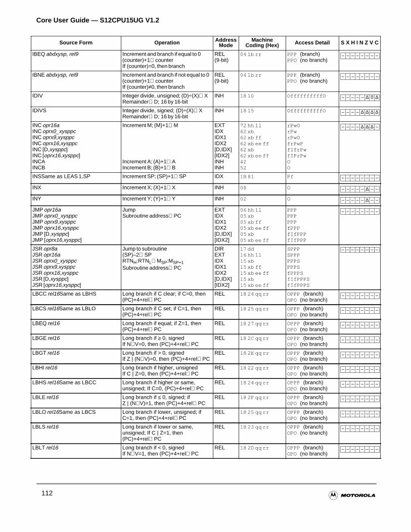
Core User Guide — S12CPU15UG V1.2
IBEQ abdxysp, rel9 Increment and branch if equal to 0(counter)+1⇒counterIf (counter)=0, then branch
REL(9-bit)
04 lb rr PPP (branch)PPO (no branch)
IBNE abdxysp, rel9 Increment and branch if not equal to 0(counter)+1⇒counterIf (counter)≠0, then branch
REL(9-bit)
04 lb rr PPP (branch)PPO (no branch)
IDIV Integer divide, unsigned; (D)÷(X)⇒XRemainder⇒D; 16 by 16-bit
INH 18 10 OffffffffffO
IDIVS Integer divide, signed; (D)÷(X)⇒XRemainder⇒D; 16 by 16-bit
INH 18 15 OffffffffffO
INC opr16aINC oprx0_xysppcINC oprx9,xysppcINC oprx16,xysppcINC [D,xysppc]INC [oprx16,xysppc]INCAINCB
Increment M; (M)+1⇒M
Increment A; (A)+1⇒AIncrement B; (B)+1⇒B
EXTIDXIDX1IDX2[D,IDX][IDX2]INHINH
72 hh ll62 xb62 xb ff62 xb ee ff62 xb62 xb ee ff4252
rPwOrPwrPwOfrPwPfIfrPwfIPrPwOO
INSSame as LEAS 1,SP Increment SP; (SP)+1⇒SP IDX 1B 81 Pf
INX Increment X; (X)+1⇒X INH 08 O
INY Increment Y; (Y)+1⇒Y INH 02 O
JMP opr16aJMP oprx0_xysppcJMP oprx9,xysppcJMP oprx16,xysppcJMP [D,xysppc]JMP [oprx16,xysppc]
JumpSubroutine address⇒PC
EXTIDXIDX1IDX2[D,IDX][IDX2]
06 hh ll05 xb05 xb ff05 xb ee ff05 xb05 xb ee ff
PPPPPPPPPfPPPfIfPPPfIfPPP
JSR opr8aJSR opr16aJSR oprx0_xysppcJSR oprx9,xysppcJSR oprx16,xysppcJSR [D,xysppc]JSR [oprx16,xysppc]
Jump to subroutine(SP)–2⇒SPRTNH:RTNL⇒MSP:MSP+1Subroutine address⇒PC
DIREXTIDXIDX1IDX2[D,IDX][IDX2]
17 dd16 hh ll15 xb15 xb ff15 xb ee ff15 xb15 xb ee ff
SPPPSPPPPPPSPPPSfPPPSfIfPPPSfIfPPPS
LBCC rel16Same as LBHS Long branch if C clear; if C=0, then(PC)+4+rel⇒PC
REL 18 24 qq rr OPPP (branch)OPO (no branch)
LBCS rel16Same as LBLO Long branch if C set; if C=1, then(PC)+4+rel⇒PC
REL 18 25 qq rr OPPP (branch)OPO (no branch)
LBEQ rel16 Long branch if equal; if Z=1, then(PC)+4+rel⇒PC
REL 18 27 qq rr OPPP (branch)OPO (no branch)
LBGE rel16 Long branch if ≥ 0, signedIf N⊕V=0, then (PC)+4+rel⇒PC
REL 18 2C qq rr OPPP (branch)OPO (no branch)
LBGT rel16 Long branch if > 0, signedIf Z | (N⊕V)=0, then (PC)+4+rel⇒PC
REL 18 2E qq rr OPPP (branch)OPO (no branch)
LBHI rel16 Long branch if higher, unsignedIf C | Z=0, then (PC)+4+rel⇒PC
REL 18 22 qq rr OPPP (branch)OPO (no branch)
LBHS rel16Same as LBCC Long branch if higher or same,unsigned; If C=0, (PC)+4+rel⇒PC
REL 18 24 qq rr OPPP (branch)OPO (no branch)
LBLE rel16 Long branch if ≤ 0, signed; ifZ | (N⊕V)=1, then (PC)+4+rel⇒PC
REL 18 2F qq rr OPPP (branch)OPO (no branch)
LBLO rel16Same as LBCS Long branch if lower, unsigned; ifC=1, then (PC)+4+rel⇒PC
REL 18 25 qq rr OPPP (branch)OPO (no branch)
LBLS rel16 Long branch if lower or same,unsigned; If C | Z=1, then(PC)+4+rel⇒PC
REL 18 23 qq rr OPPP (branch)OPO (no branch)
LBLT rel16 Long branch if < 0, signedIf N⊕V=1, then (PC)+4+rel⇒PC
REL 18 2D qq rr OPPP (branch)OPO (no branch)
Source Form Operation AddressMode
MachineCoding (Hex) Access Detail S X H I N Z V C
– – – – – – – –
– – – – – – – –
– – – – – ∆ 0 ∆
– – – – ∆ ∆ ∆ ∆
– – – – ∆ ∆ ∆ –
– – – – – – – –
– – – – – ∆ – –
– – – – – ∆ – –
– – – – – – – –
– – – – – – – –
– – – – – – – –
– – – – – – – –
– – – – – – – –
– – – – – – – –
– – – – – – – –
– – – – – – – –
– – – – – – – –
– – – – – – – –
– – – – – – – –
– – – – – – – –
– – – – – – – –
112
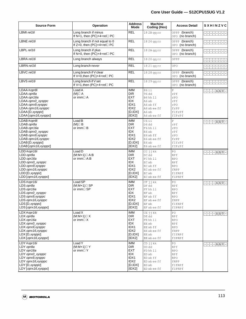
Core User Guide — S12CPU15UG V1.2
LBMI rel16 Long branch if minusIf N=1, then (PC)+4+rel⇒PC
REL 18 2B qq rr OPPP (branch)OPO (no branch)
LBNE rel16 Long branch if not equal to 0If Z=0, then (PC)+4+rel⇒PC
REL 18 26 qq rr OPPP (branch)OPO (no branch)
LBPL rel16 Long branch if plusIf N=0, then (PC)+4+rel⇒PC
REL 18 2A qq rr OPPP (branch)OPO (no branch)
LBRA rel16 Long branch always REL 18 20 qq rr OPPP
LBRN rel16 Long branch never REL 18 21 qq rr OPO
LBVC rel16 Long branch if V clearIf V=0,then (PC)+4+rel⇒PC
REL 18 28 qq rr OPPP (branch)OPO (no branch)
LBVS rel16 Long branch if V setIf V=1,then (PC)+4+rel⇒PC
REL 18 29 qq rr OPPP (branch)OPO (no branch)
LDAA #opr8iLDAA opr8aLDAA opr16aLDAA oprx0_xysppcLDAA oprx9,xysppcLDAA oprx16,xysppcLDAA [D,xysppc]LDAA [oprx16,xysppc]
Load A(M)⇒Aor imm⇒A
IMMDIREXTIDXIDX1IDX2[D,IDX][IDX2]
86 ii96 ddB6 hh llA6 xbA6 xb ffA6 xb ee ffA6 xbA6 xb ee ff
PrPfrPOrPfrPOfrPPfIfrPffIPrPf
LDAB #opr8iLDAB opr8aLDAB opr16aLDAB oprx0_xysppcLDAB oprx9,xysppcLDAB oprx16,xysppcLDAB [D,xysppc]LDAB [oprx16,xysppc]
Load B(M)⇒Bor imm⇒B
IMMDIREXTIDXIDX1IDX2[D,IDX][IDX2]
C6 iiD6 ddF6 hh llE6 xbE6 xb ffE6 xb ee ffE6 xbE6 xb ee ff
PrPfrPOrPfrPOfrPPfIfrPffIPrPf
LDD #opr16iLDD opr8aLDD opr16aLDD oprx0_xysppcLDD oprx9,xysppcLDD oprx16,xysppcLDD [D,xysppc]LDD [oprx16,xysppc]
Load D(M:M+1)⇒A:Bor imm⇒A:B
IMMDIREXTIDXIDX1IDX2[D,IDX][IDX2]
CC jj kkDC ddFC hh llEC xbEC xb ffEC xb ee ffEC xbEC xb ee ff
PORPfRPORPfRPOfRPPfIfRPffIPRPf
LDS #opr16iLDS opr8aLDS opr16aLDS oprx0_xysppcLDS oprx9,xysppcLDS oprx16,xysppcLDS [D,xysppc]LDS [oprx16,xysppc]
Load SP(M:M+1)⇒SPor imm⇒SP
IMMDIREXTIDXIDX1IDX2[D,IDX][IDX2]
CF jj kkDF ddFF hh llEF xbEF xb ffEF xb ee ffEF xbEF xb ee ff
PORPfRPORPfRPOfRPPfIfRPffIPRPf
LDX #opr16iLDX opr8aLDX opr16aLDX oprx0_xysppcLDX oprx9,xysppcLDX oprx16,xysppcLDX [D,xysppc]LDX [oprx16,xysppc]
Load X(M:M+1)⇒Xor imm⇒X
IMMDIREXTIDXIDX1IDX2[D,IDX][IDX2]
CE jj kkDE ddFE hh llEE xbEE xb ffEE xb ee ffEE xbEE xb ee ff
PORPfRPORPfRPOfRPPfIfRPffIPRPf
LDY #opr16iLDY opr8aLDY opr16aLDY oprx0_xysppcLDY oprx9,xysppcLDY oprx16,xysppcLDY [D,xysppc]LDY [oprx16,xysppc]
Load Y(M:M+1)⇒Yor imm⇒Y
IMMDIREXTIDXIDX1IDX2[D,IDX][IDX2]
CD jj kkDD ddFD hh llED xbED xb ffED xb ee ffED xbED xb ee ff
PORPfRPORPfRPOfRPPfIfRPffIPRPf
Source Form Operation AddressMode
MachineCoding (Hex) Access Detail S X H I N Z V C
– – – – – – – –
– – – – – – – –
– – – – – – – –
– – – – – – – –
– – – – – – – –
– – – – – – – –
– – – – – – – –
– – – – ∆ ∆ 0 –
– – – – ∆ ∆ 0 –
– – – – ∆ ∆ 0 –
– – – – ∆ ∆ 0 –
– – – – ∆ ∆ 0 –
– – – – ∆ ∆ 0 –
113
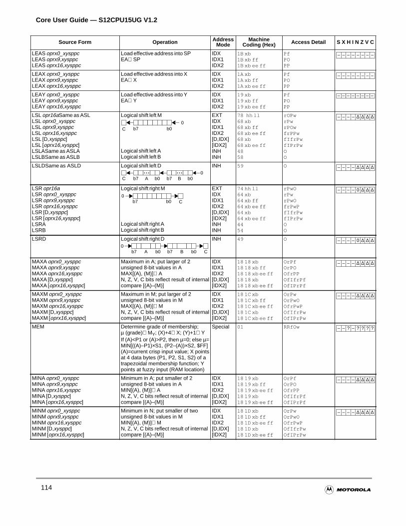
Core User Guide — S12CPU15UG V1.2
LEAS oprx0_xysppcLEAS oprx9,xysppcLEAS oprx16,xysppc
Load effective address into SPEA⇒SP
IDXIDX1IDX2
1B xb1B xb ff1B xb ee ff
PfPOPP
LEAX oprx0_xysppcLEAX oprx9,xysppcLEAX oprx16,xysppc
Load effective address into XEA⇒X
IDXIDX1IDX2
1A xb1A xb ff1A xb ee ff
PfPOPP
LEAY oprx0_xysppcLEAY oprx9,xysppcLEAY oprx16,xysppc
Load effective address into YEA⇒Y
IDXIDX1IDX2
19 xb19 xb ff19 xb ee ff
PfPOPP
LSL opr16aSame as ASLLSL oprx0_xysppcLSL oprx9,xysppcLSL oprx16,xysppcLSL [D,xysppc]LSL [oprx16,xysppc]LSLASame as ASLALSLBSame as ASLB
Logical shift left M
Logical shift left ALogical shift left B
EXTIDXIDX1IDX2[D,IDX][IDX2]INHINH
78 hh ll68 xb68 xb ff68 xb ee ff68 xb68 xb ee ff4858
rOPwrPwrPOwfrPPwfIfrPwfIPrPwOO
LSLDSame as ASLD Logical shift left D INH 59 O
LSR opr16aLSR oprx0_xysppcLSR oprx9,xysppcLSR oprx16,xysppcLSR [D,xysppc]LSR [oprx16,xysppc]LSRALSRB
Logical shift right M
Logical shift right ALogical shift right B
EXTIDXIDX1IDX2[D,IDX][IDX2]INHINH
74 hh ll64 xb64 xb ff64 xb ee ff64 xb64 xb ee ff4454
rPwOrPwrPwOfrPwPfIfrPwfIPrPwOO
LSRD Logical shift right D INH 49 O
MAXA oprx0_xysppcMAXA oprx9,xysppcMAXA oprx16,xysppcMAXA [D,xysppc]MAXA [oprx16,xysppc]
Maximum in A; put larger of 2unsigned 8-bit values in AMAX[(A), (M)]⇒AN, Z, V, C bits reflect result of internalcompare [(A)–(M)]
IDXIDX1IDX2[D,IDX][IDX2]
18 18 xb18 18 xb ff18 18 xb ee ff18 18 xb18 18 xb ee ff
OrPfOrPOOfrPPOfIfrPfOfIPrPf
MAXM oprx0_xysppcMAXM oprx9,xysppcMAXM oprx16,xysppcMAXM [D,xysppc]MAXM [oprx16,xysppc]
Maximum in M; put larger of 2unsigned 8-bit values in MMAX[(A), (M)]⇒MN, Z, V, C bits reflect result of internalcompare [(A)–(M)]
IDXIDX1IDX2[D,IDX][IDX2]
18 1C xb18 1C xb ff18 1C xb ee ff18 1C xb18 1C xb ee ff
OrPwOrPwOOfrPwPOfIfrPwOfIPrPw
MEM Determine grade of membership;µ (grade)⇒MY; (X)+4⇒X; (Y)+1⇒YIf (A)<P1 or (A)>P2, then µ=0; else µ=MIN[((A)–P1)×S1, (P2–(A))×S2, $FF](A)=current crisp input value; X pointsat 4 data bytes (P1, P2, S1, S2) of atrapezoidal membership function; Ypoints at fuzzy input (RAM location)
Special 01 RRfOw
MINA oprx0_xysppcMINA oprx9,xysppcMINA oprx16,xysppcMINA [D,xysppc]MINA [oprx16,xysppc]
Minimum in A; put smaller of 2unsigned 8-bit values in AMIN[(A), (M)]⇒AN, Z, V, C bits reflect result of internalcompare [(A)–(M)]
IDXIDX1IDX2[D,IDX][IDX2]
18 19 xb18 19 xb ff18 19 xb ee ff18 19 xb18 19 xb ee ff
OrPfOrPOOfrPPOfIfrPfOfIPrPf
MINM oprx0_xysppcMINM oprx9,xysppcMINM oprx16,xysppcMINM [D,xysppc]MINM [oprx16,xysppc]
Minimum in N; put smaller of twounsigned 8-bit values in MMIN[(A), (M)]⇒MN, Z, V, C bits reflect result of internalcompare [(A)–(M)]
IDXIDX1IDX2[D,IDX][IDX2]
18 1D xb18 1D xb ff18 1D xb ee ff18 1D xb18 1D xb ee ff
OrPwOrPwOOfrPwPOfIfrPwOfIPrPw
Source Form Operation AddressMode
MachineCoding (Hex) Access Detail S X H I N Z V C
– – – – – – – –
– – – – – – – –
– – – – – – – –
C0
b7 b0
– – – – ∆ ∆ ∆ ∆
C0
b7 b0A Bb7b0• • • • • •
– – – – ∆ ∆ ∆ ∆
C0
b7 b0
– – – – 0 ∆ ∆ ∆
Cb7 b0A Bb7b00
– – – – 0 ∆ ∆ ∆
– – – – ∆ ∆ ∆ ∆
– – – – ∆ ∆ ∆ ∆
– – ? – ? ? ? ?
– – – – ∆ ∆ ∆ ∆
– – – – ∆ ∆ ∆ ∆
114
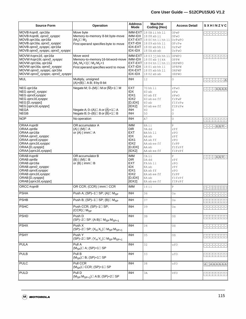
Core User Guide — S12CPU15UG V1.2
MOVB #opr8, opr16aMOVB #opr8i, oprx0_xysppcMOVB opr16a, opr16aMOVB opr16a, oprx0_xysppcMOVB oprx0_xysppc, opr16aMOVB oprx0_xysppc, oprx0_xysppc
Move byteMemory-to-memory 8-bit byte-move(M1)⇒M2First operand specifies byte to move
IMM-EXTIMM-IDXEXT-EXTEXT-IDXIDX-EXTIDX-IDX
18 0B ii hh ll18 08 xb ii18 0C hh ll hh ll18 09 xb hh ll18 0D xb hh ll18 0A xb xb
OPwPOPwOOrPwPOOPrPwOrPwPOrPwO
MOVW #oprx16, opr16aMOVW #opr16i, oprx0_xysppcMOVW opr16a, opr16aMOVW opr16a, oprx0_xysppcMOVW oprx0_xysppc, opr16aMOVW oprx0_xysppc, oprx0_xysppc
Move wordMemory-to-memory16-bitword-move(M1:M1+1)⇒M2:M2+1First operand specifies word to move
IMM-EXTIMM-IDXEXT-EXTEXT-IDXIDX-EXTIDX-IDX
18 03 jj kk hh ll18 00 xb jj kk18 04 hh ll hh ll18 01 xb hh ll18 05 xb hh ll18 02 xb xb
OPWPOOPPWORPWPOOPRPWORPWPORPWO
MUL Multiply, unsigned(A)×(B)⇒A:B; 8 by 8-bit
INH 12 O
NEG opr16aNEG oprx0_xysppcNEG oprx9,xysppcNEG oprx16,xysppcNEG [D,xysppc]NEG [oprx16,xysppc]NEGANEGB
Negate M; 0–(M)⇒M or (M)+1⇒M
Negate A; 0–(A)⇒A or (A)+1⇒ANegate B; 0–(B)⇒B or (B)+1⇒B
EXTIDXIDX1IDX2[D,IDX][IDX2]INHINH
70 hh ll60 xb60 xb ff60 xb ee ff60 xb60 xb ee ff4050
rPwOrPwrPwOfrPwPfIfrPwfIPrPwOO
NOP No operation INH A7 O
ORAA #opr8iORAA opr8aORAA opr16aORAA oprx0_xysppcORAA oprx9,xysppcORAA oprx16,xysppcORAA [D,xysppc]ORAA [oprx16,xysppc]
OR accumulator A(A) | (M)⇒Aor (A) | imm⇒A
IMMDIREXTIDXIDX1IDX2[D,IDX][IDX2]
8A ii9A ddBA hh llAA xbAA xb ffAA xb ee ffAA xbAA xb ee ff
PrPfrPOrPfrPOfrPPfIfrPffIPrPf
ORAB #opr8iORAB opr8aORAB opr16aORAB oprx0_xysppcORAB oprx9,xysppcORAB oprx16,xysppcORAB [D,xysppc]ORAB [oprx16,xysppc]
OR accumulator B(B) | (M)⇒Bor (B) | imm⇒B
IMMDIREXTIDXIDX1IDX2[D,IDX][IDX2]
CA iiDA ddFA hh llEA xbEA xb ffEA xb ee ffEA xbEA xb ee ff
PrPfrPOrPfrPOfrPPfIfrPffIPrPf
ORCC #opr8i OR CCR; (CCR) | imm⇒CCR IMM 14 ii P
PSHA Push A; (SP)–1⇒SP; (A)⇒MSP INH 36 Os
PSHB Push B; (SP)–1⇒SP; (B)⇒MSP INH 37 Os
PSHC Push CCR; (SP)–1⇒SP;(CCR)⇒MSP
INH 39 Os
PSHD Push D(SP)–2⇒SP; (A:B)⇒MSP:MSP+1
INH 3B OS
PSHX Push X(SP)–2⇒SP; (XH:XL)⇒MSP:MSP+1
INH 34 OS
PSHY Push Y(SP)–2⇒SP; (YH:YL)⇒MSP:MSP+1
INH 35 OS
PULA Pull A(MSP)⇒A; (SP)+1⇒SP
INH 32 ufO
PULB Pull B(MSP)⇒B; (SP)+1⇒SP
INH 33 ufO
PULC Pull CCR(MSP)⇒CCR; (SP)+1⇒SP
INH 38 ufO
PULD Pull D(MSP:MSP+1)⇒A:B; (SP)+2⇒SP
INH 3A UfO
Source Form Operation AddressMode
MachineCoding (Hex) Access Detail S X H I N Z V C
– – – – – – – –
– – – – – – – –
– – – – – – – ∆
– – – – ∆ ∆ ∆ ∆
– – – – – – – –
– – – – ∆ ∆ 0 –
– – – – ∆ ∆ 0 –
⇑ – ⇑ ⇑ ⇑ ⇑ ⇑ ⇑
– – – – – – – –
– – – – – – – –
– – – – – – – –
– – – – – – – –
– – – – – – – –
– – – – – – – –
– – – – – – – –
– – – – – – – –
∆ ⇓ ∆ ∆ ∆ ∆ ∆ ∆
– – – – – – – –
115
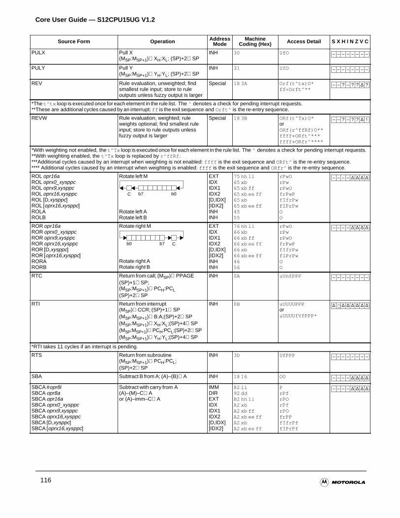
Core User Guide — S12CPU15UG V1.2
PULX Pull X(MSP:MSP+1)⇒XH:XL; (SP)+2⇒SP
INH 30 UfO
PULY Pull Y(MSP:MSP+1)⇒YH:YL; (SP)+2⇒SP
INH 31 UfO
REV Rule evaluation, unweighted; findsmallest rule input; store to ruleoutputs unless fuzzy output is larger
Special 18 3A Orf(t^tx)O*ff+Orft^**
*The t^tx loop is executed once for each element in the rule list. The ^ denotes a check for pending interrupt requests.**These are additional cycles caused by an interrupt: ff is the exit sequence and Orft^ is the re-entry sequence.
REVW Rule evaluation, weighted; ruleweights optional; find smallest ruleinput; store to rule outputs unlessfuzzy output is larger
Special 18 3B ORf(t^Tx)O*orORf(r^ffRf)O**ffff+ORft^***ffff+ORfr^****
*With weighting not enabled, the t^Tx loop is executed once for each element in the rule list. The ^ denotes a check for pending interrupt requests.**With weighting enabled, the t^Tx loop is replaced by r^ffRf .***Additional cycles caused by an interrupt when weighting is not enabled: ffff is the exit sequence and ORft^ is the re-entry sequence.**** Additional cycles caused by an interrupt when weighting is enabled: ffff is the exit sequence and ORfr^ is the re-entry sequence.
ROL opr16aROL oprx0_xysppcROL oprx9,xysppcROL oprx16,xysppcROL [D,xysppc]ROL [oprx16,xysppc]ROLAROLB
Rotate left M
Rotate left ARotate left B
EXTIDXIDX1IDX2[D,IDX][IDX2]INHINH
75 hh ll65 xb65 xb ff65 xb ee ff65 xb65 xb ee ff4555
rPwOrPwrPwOfrPwPfIfrPwfIPrPwOO
ROR opr16aROR oprx0_xysppcROR oprx9,xysppcROR oprx16,xysppcROR [D,xysppc]ROR [oprx16,xysppc]RORARORB
Rotate right M
Rotate right ARotate right B
EXTIDXIDX1IDX2[D,IDX][IDX2]INHINH
76 hh ll66 xb66 xb ff66 xb ee ff66 xb66 xb ee ff4656
rPwOrPwrPwOfrPwPfIfrPwfIPrPwOO
RTC Return from call; (MSP)⇒PPAGE(SP)+1⇒SP;(MSP:MSP+1)⇒PCH:PCL(SP)+2⇒SP
INH 0A uUnfPPP
RTI Return from interrupt(MSP)⇒CCR; (SP)+1⇒SP(MSP:MSP+1)⇒B:A;(SP)+2⇒SP(MSP:MSP+1)⇒XH:XL;(SP)+4⇒SP(MSP:MSP+1)⇒PCH:PCL;(SP)+2⇒SP(MSP:MSP+1)⇒YH:YL;(SP)+4⇒SP
INH 0B uUUUUPPPoruUUUUfVfPPP*
*RTI takes 11 cycles if an interrupt is pending.
RTS Return from subroutine(MSP:MSP+1)⇒PCH:PCL;(SP)+2⇒SP
INH 3D UfPPP
SBA Subtract B from A; (A)–(B)⇒A INH 18 16 OO
SBCA #opr8iSBCA opr8aSBCA opr16aSBCA oprx0_xysppcSBCA oprx9,xysppcSBCA oprx16,xysppcSBCA [D,xysppc]SBCA [oprx16,xysppc]
Subtract with carry from A(A)–(M)–C⇒Aor (A)–imm–C⇒A
IMMDIREXTIDXIDX1IDX2[D,IDX][IDX2]
82 ii92 ddB2 hh llA2 xbA2 xb ffA2 xb ee ffA2 xbA2 xb ee ff
PrPfrPOrPfrPOfrPPfIfrPffIPrPf
Source Form Operation AddressMode
MachineCoding (Hex) Access Detail S X H I N Z V C
– – – – – – – –
– – – – – – – –
– – ? – ? ? ∆ ?
– – ? – ? ? ∆ !
C b7 b0
– – – – ∆ ∆ ∆ ∆
Cb7b0
– – – – ∆ ∆ ∆ ∆
– – – – – – – –
∆ ⇓ ∆ ∆ ∆ ∆ ∆ ∆
– – – – – – – –
– – – – ∆ ∆ ∆ ∆
– – – – ∆ ∆ ∆ ∆
116
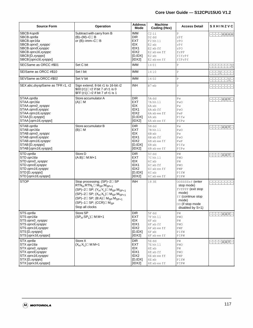
Core User Guide — S12CPU15UG V1.2
SBCB #opr8iSBCB opr8aSBCB opr16aSBCB oprx0_xysppcSBCB oprx9,xysppcSBCB oprx16,xysppcSBCB [D,xysppc]SBCB [oprx16,xysppc]
Subtract with carry from B(B)–(M)–C⇒Bor (B)–imm–C⇒B
IMMDIREXTIDXIDX1IDX2[D,IDX][IDX2]
C2 iiD2 ddF2 hh llE2 xbE2 xb ffE2 xb ee ffE2 xbE2 xb ee ff
PrPfrPOrPfrPOfrPPfIfrPffIPrPf
SECSame as ORCC #$01 Set C bit IMM 14 01 P
SEISame as ORCC #$10 Set I bit IMM 14 10 P
SEVSame as ORCC #$02 Set V bit IMM 14 02 P
SEX abc,dxyspSame as TFR r1, r2 Sign extend; 8-bit r1 to 16-bit r2$00:(r1)⇒r2 if bit 7 of r1 is 0$FF:(r1)⇒r2 if bit 7 of r1 is 1
INH B7 eb P
STAA opr8aSTAA opr16aSTAA oprx0_xysppcSTAA oprx9,xysppcSTAA oprx16,xysppcSTAA [D,xysppc]STAA [oprx16,xysppc]
Store accumulator A(A)⇒M
DIREXTIDXIDX1IDX2[D,IDX][IDX2]
5A dd7A hh ll6A xb6A xb ff6A xb ee ff6A xb6A xb ee ff
PwPwOPwPwOPwPPIfwPIPw
STAB opr8aSTAB opr16aSTAB oprx0_xysppcSTAB oprx9,xysppcSTAB oprx16,xysppcSTAB [D,xysppc]STAB [oprx16,xysppc]
Store accumulator B(B)⇒M
DIREXTIDXIDX1IDX2[D,IDX][IDX2]
5B dd7B hh ll6B xb6B xb ff6B xb ee ff6B xb6B xb ee ff
PwPwOPwPwOPwPPIfwPIPw
STD opr8aSTD opr16aSTD oprx0_xysppcSTD oprx9,xysppcSTD oprx16,xysppcSTD [D,xysppc]STD [oprx16,xysppc]
Store D(A:B)⇒M:M+1
DIREXTIDXIDX1IDX2[D,IDX][IDX2]
5C dd7C hh ll6C xb6C xb ff6C xb ee ff6C xb6C xb ee ff
PWPWOPWPWOPWPPIfWPIPW
STOP Stop processing; (SP)–2⇒SPRTNH:RTNL⇒MSP:MSP+1(SP)–2⇒SP; (YH:YL)⇒MSP:MSP+1(SP)–2⇒SP; (XH:XL)⇒MSP:MSP+1(SP)–2⇒SP; (B:A)⇒MSP:MSP+1(SP)–1⇒SP; (CCR)⇒MSPStop all clocks
INH 18 3E OOSSSSsf (enterstop mode)
fVfPPP (exit stopmode)
ff (continue stopmode)
OO (if stop modedisabled by S=1)
STS opr8aSTS opr16aSTS oprx0_xysppcSTS oprx9,xysppcSTS oprx16,xysppcSTS [D,xysppc]STS [oprx16,xysppc]
Store SP(SPH:SPL)⇒M:M+1
DIREXTIDXIDX1IDX2[D,IDX][IDX2]
5F dd7F hh ll6F xb6F xb ff6F xb ee ff6F xb6F xb ee ff
PWPWOPWPWOPWPPIfWPIPW
STX opr8aSTX opr16aSTX oprx0_xysppcSTX oprx9,xysppcSTX oprx16,xysppcSTX [D,xysppc]STX [oprx16,xysppc]
Store X(XH:XL)⇒M:M+1
DIREXTIDXIDX1IDX2[D,IDX][IDX2]
5E dd7E hh ll6E xb6E xb ff6E xb ee ff6E xb6E xb ee ff
PWPWOPWPWOPWPPIfWPIPW
Source Form Operation AddressMode
MachineCoding (Hex) Access Detail S X H I N Z V C
– – – – ∆ ∆ ∆ ∆
– – – – – – – 1
– – – 1 – – – –
– – – – – – 1 –
– – – – – – – –
– – – – ∆ ∆ 0 –
– – – – ∆ ∆ 0 –
– – – – ∆ ∆ 0 –
– – – – – – – –
– – – – ∆ ∆ 0 –
– – – – ∆ ∆ 0 –
117
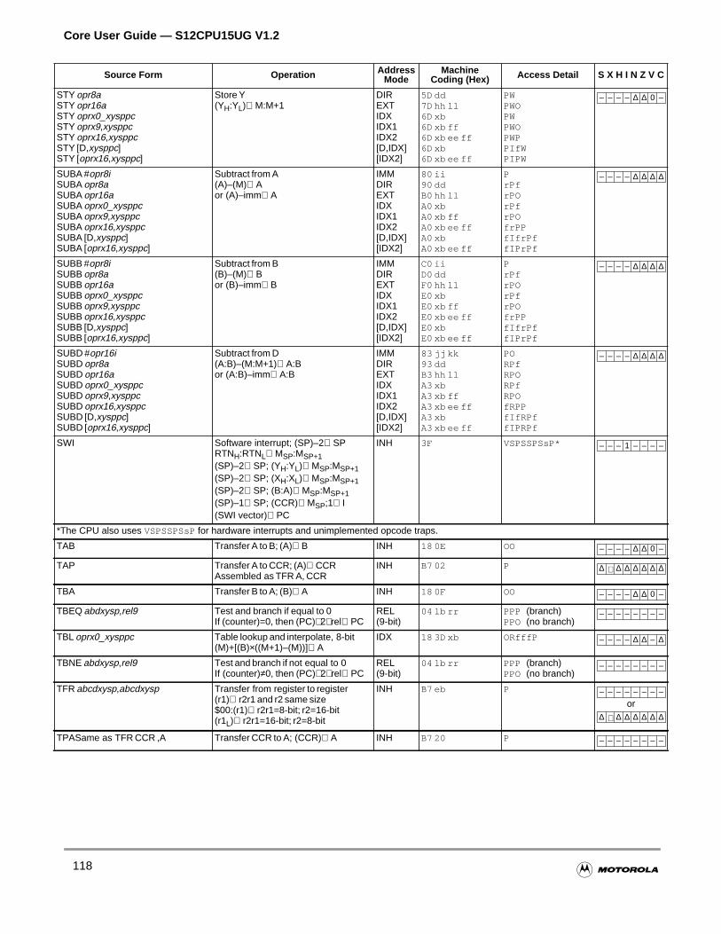
Core User Guide — S12CPU15UG V1.2
STY opr8aSTY opr16aSTY oprx0_xysppcSTY oprx9,xysppcSTY oprx16,xysppcSTY [D,xysppc]STY [oprx16,xysppc]
Store Y(YH:YL)⇒M:M+1
DIREXTIDXIDX1IDX2[D,IDX][IDX2]
5D dd7D hh ll6D xb6D xb ff6D xb ee ff6D xb6D xb ee ff
PWPWOPWPWOPWPPIfWPIPW
SUBA #opr8iSUBA opr8aSUBA opr16aSUBA oprx0_xysppcSUBA oprx9,xysppcSUBA oprx16,xysppcSUBA [D,xysppc]SUBA [oprx16,xysppc]
Subtract from A(A)–(M)⇒Aor (A)–imm⇒A
IMMDIREXTIDXIDX1IDX2[D,IDX][IDX2]
80 ii90 ddB0 hh llA0 xbA0 xb ffA0 xb ee ffA0 xbA0 xb ee ff
PrPfrPOrPfrPOfrPPfIfrPffIPrPf
SUBB #opr8iSUBB opr8aSUBB opr16aSUBB oprx0_xysppcSUBB oprx9,xysppcSUBB oprx16,xysppcSUBB [D,xysppc]SUBB [oprx16,xysppc]
Subtract from B(B)–(M)⇒Bor (B)–imm⇒B
IMMDIREXTIDXIDX1IDX2[D,IDX][IDX2]
C0 iiD0 ddF0 hh llE0 xbE0 xb ffE0 xb ee ffE0 xbE0 xb ee ff
PrPfrPOrPfrPOfrPPfIfrPffIPrPf
SUBD #opr16iSUBD opr8aSUBD opr16aSUBD oprx0_xysppcSUBD oprx9,xysppcSUBD oprx16,xysppcSUBD [D,xysppc]SUBD [oprx16,xysppc]
Subtract from D(A:B)–(M:M+1)⇒A:Bor (A:B)–imm⇒A:B
IMMDIREXTIDXIDX1IDX2[D,IDX][IDX2]
83 jj kk93 ddB3 hh llA3 xbA3 xb ffA3 xb ee ffA3 xbA3 xb ee ff
PORPfRPORPfRPOfRPPfIfRPffIPRPf
SWI Software interrupt; (SP)–2⇒SPRTNH:RTNL⇒MSP:MSP+1(SP)–2⇒SP; (YH:YL)⇒MSP:MSP+1(SP)–2⇒SP; (XH:XL)⇒MSP:MSP+1(SP)–2⇒SP; (B:A)⇒MSP:MSP+1(SP)–1⇒SP; (CCR)⇒MSP;1⇒I(SWI vector)⇒PC
INH 3F VSPSSPSsP*
*The CPU also uses VSPSSPSsP for hardware interrupts and unimplemented opcode traps.
TAB Transfer A to B; (A)⇒B INH 18 0E OO
TAP Transfer A to CCR; (A)⇒CCRAssembled as TFR A, CCR
INH B7 02 P
TBA Transfer B to A; (B)⇒A INH 18 0F OO
TBEQ abdxysp,rel9 Test and branch if equal to 0If (counter)=0, then (PC)+2+rel⇒PC
REL(9-bit)
04 lb rr PPP (branch)PPO (no branch)
TBL oprx0_xysppc Table lookup and interpolate, 8-bit(M)+[(B)×((M+1)–(M))]⇒A
IDX 18 3D xb ORfffP
TBNE abdxysp,rel9 Test and branch if not equal to 0If (counter)≠0, then (PC)+2+rel⇒PC
REL(9-bit)
04 lb rr PPP (branch)PPO (no branch)
TFR abcdxysp,abcdxysp Transfer from register to register(r1)⇒r2r1 and r2 same size$00:(r1)⇒r2r1=8-bit; r2=16-bit(r1L)⇒r2r1=16-bit; r2=8-bit
INH B7 eb P
or
TPASame as TFR CCR ,A Transfer CCR to A; (CCR)⇒A INH B7 20 P
Source Form Operation AddressMode
MachineCoding (Hex) Access Detail S X H I N Z V C
– – – – ∆ ∆ 0 –
– – – – ∆ ∆ ∆ ∆
– – – – ∆ ∆ ∆ ∆
– – – – ∆ ∆ ∆ ∆
– – – 1 – – – –
– – – – ∆ ∆ 0 –
∆ ⇓ ∆ ∆ ∆ ∆ ∆ ∆
– – – – ∆ ∆ 0 –
– – – – – – – –
– – – – ∆ ∆ – ∆
– – – – – – – –
– – – – – – – –
∆ ⇓ ∆ ∆ ∆ ∆ ∆ ∆
– – – – – – – –
118
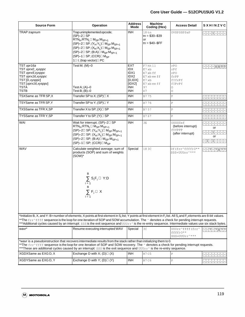
Core User Guide — S12CPU15UG V1.2
TRAP trapnum Trapunimplementedopcode;(SP)–2⇒SPRTNH:RTNL⇒MSP:MSP+1(SP)–2⇒SP; (YH:YL)⇒MSP:MSP+1(SP)–2⇒SP; (XH:XL)⇒MSP:MSP+1(SP)–2⇒SP; (B:A)⇒MSP:MSP+1(SP)–1⇒SP; (CCR)⇒MSP1⇒I; (trap vector)⇒PC
INH 18 tntn = $30–$39ortn = $40–$FF
OVSPSSPSsP
TST opr16aTST oprx0_xysppcTST oprx9,xysppcTST oprx16,xysppcTST [D,xysppc]TST [oprx16,xysppc]TSTATSTB
Test M; (M)–0
Test A; (A)–0Test B; (B)–0
EXTIDXIDX1IDX2[D,IDX][IDX2]INHINH
F7 hh llE7 xbE7 xb ffE7 xb ee ffE7 xbE7 xb ee ff97D7
rPOrPfrPOfrPPfIfrPffIPrPfOO
TSXSame as TFR SP,X Transfer SP to X; (SP)⇒X INH B7 75 P
TSYSame as TFR SP,Y Transfer SP to Y; (SP)⇒Y INH B7 76 P
TXSSame as TFR X,SP Transfer X to SP; (X)⇒SP INH B7 57 P
TYSSame as TFR Y,SP Transfer Y to SP; (Y)⇒SP INH B7 67 P
WAI Wait for interrupt; (SP)–2⇒SPRTNH:RTNL⇒MSP:MSP+1(SP)–2⇒SP; (YH:YL)⇒MSP:MSP+1(SP)–2⇒SP; (XH:XL)⇒MSP:MSP+1(SP)–2⇒SP; (B:A)⇒MSP:MSP+1(SP)–1⇒SP; (CCR)⇒MSP
INH 3E OSSSSsf(before interrupt)
fVfPPP(after interrupt)
or
or
WAV Calculate weighted average; sum ofproducts (SOP) and sum of weights(SOW)*
Special 18 3C Of(frr^ffff)O**SSS+UUUrr^***
*Initialize B, X, and Y: B=number of elements; X points at first element in Si list; Y points at first element in Fi list. All Si and Fi elements are 8-bit values.**The frr^ffff sequence is the loop for one iteration of SOP and SOW accumulation. The ^ denotes a check for pending interrupt requests.***Additional cycles caused by an interrupt: SSSis the exit sequence and UUUrr^ is the re-entry sequence. Intermediate values use six stack bytes.
wavr* Resume executing interrupted WAV Special 3C UUUrr^ffff(frr^ffff)O**SSS+UUUrr^***
*wavr is a pseudoinstruction that recovers intermediate results from the stack rather than initializing them to 0.**The frr^ffff sequence is the loop for one iteration of SOP and SOW recovery. The ^ denotes a check for pending interrupt requests.***These are additional cycles caused by an interrupt: SSS is the exit sequence and UUUrr^ is the re-entry sequence.
XGDXSame as EXG D, X Exchange D with X; (D)⇔(X) INH B7 C5 P
XGDYSame as EXG D, Y Exchange D with Y; (D)⇔(Y) INH B7 C6 P
Source Form Operation AddressMode
MachineCoding (Hex) Access Detail S X H I N Z V C
– – – 1 – – – –
– – – – ∆ ∆ 0 0
– – – – – – – –
– – – – – – – –
– – – – – – – –
– – – – – – – –
– – – – – – – –
– – – 1 – – – –
– 1 – 1 – – – –
Fii 1=
B
∑ X⇒
SiFii 1=
B
∑ Y:D⇒
– – ? – ? ∆ ? ?
– – ? – ? ∆ ? ?
– – – – – – – –
– – – – – – – –
119
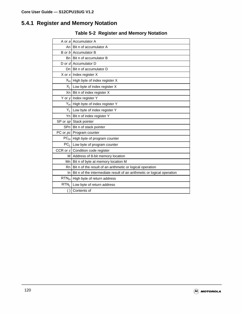
Core User Guide — S12CPU15UG V1.2
5.4.1 Register and Memory Notation
Table 5-2 Register and Memory Notation
A or a Accumulator A
An Bit n of accumulator A
B or b Accumulator B
Bn Bit n of accumulator B
D or d Accumulator D
Dn Bit n of accumulator D
X or x Index register X
XH High byte of index register X
XL Low byte of index register X
Xn Bit n of index register X
Y or y Index register Y
YH High byte of index register Y
YL Low byte of index register Y
Yn Bit n of index register Y
SP or sp Stack pointer
SPn Bit n of stack pointer
PC or pc Program counter
PCH High byte of program counter
PCL Low byte of program counter
CCR or c Condition code register
M Address of 8-bit memory location
Mn Bit n of byte at memory location M
Rn Bit n of the result of an arithmetic or logical operation
In Bit n of the intermediate result of an arithmetic or logical operation
RTNH High byte of return address
RTNL Low byte of return address
( ) Contents of
120

Core User Guide — S12CPU15UG V1.2
to the
ic is
et cannot
5.4.2 Source Form Notation
TheSource Form column of the summary inTable 5-1 gives essential information about assemblersource forms. For complete information about writing source files for a particular assembler, referdocumentation provided by the assembler vendor.
Everything in theSource Form column,except expressions in italic characters, is literal informationwhich must appear in the assembly source file exactly as shown. The initial 3- to 5-letter mnemonalways a literal expression. All commas, pound signs (#), parentheses, square brackets ( [ or ] ), plus signs(+), minus signs (–), and the register designation (A, B, D), are literal characters.
The groups of italic characters shown inTable 5-3 represent variable information to be supplied by thprogrammer. These groups can include any alphanumeric character or the underscore character, buinclude a space or comma. For example, the groupsxysppcandoprx0_xysppcare both valid, but the twogroupsoprx0 xysppc are not valid because there is a space between them.
Table 5-3 Source Form Notation
abc Register designator for A, B, or CCR
abcdxysp Register designator for A, B, CCR, D, X, Y, or SP
abd Register designator for A, B, or D
abdxysp Register designator for A, B, D, X, Y, or SP
dxysp Register designator for D, X, Y, or SP
msk88-bit mask valueSome assemblers require the # symbol before the mask value.
opr8i 8-bit immediate value
opr16i 16-bit immediate value
opr8a 8-bit address value used with direct address mode
opr16a 16-bit address value
oprx0_xysp Indexed addressing postbyte code:oprx3,–xysp — Predecrement X , Y, or SP by 1–8oprx3,+xysp — Preincrement X , Y, or SP by 1–8oprx3,xysp– — Postdecrement X, Y, or SP by 1–8oprx3,xysp+ — Postincrement X, Y, or SP by 1–8oprx5,xysppc — 5-bit constant offset from X, Y, SP, or PCabd,xysppc — Accumulator A, B, or D offset from X, Y, SP, or PC
oprx3 Any positive integer from 1 to 8 for pre/post increment/decrement
oprx5 Any integer from –16 to +15
oprx9 Any integer from –256 to +255
oprx16 Any integer from –32,768 to +65,535
page8-bit value for PPAGE registerSome assemblers require the # symbol before this value.
rel8 Label of branch destination within –256 to +255 locations
rel9 Label of branch destination within –512 to +511 locations
rel16 Any label within the 64K byte memory space
trapnum Any 8-bit integer from $30 to $39 or from $40 to $FF
xysp Register designator for X or Y or SP
xysppc Register designator for X or Y or SP or PC
121
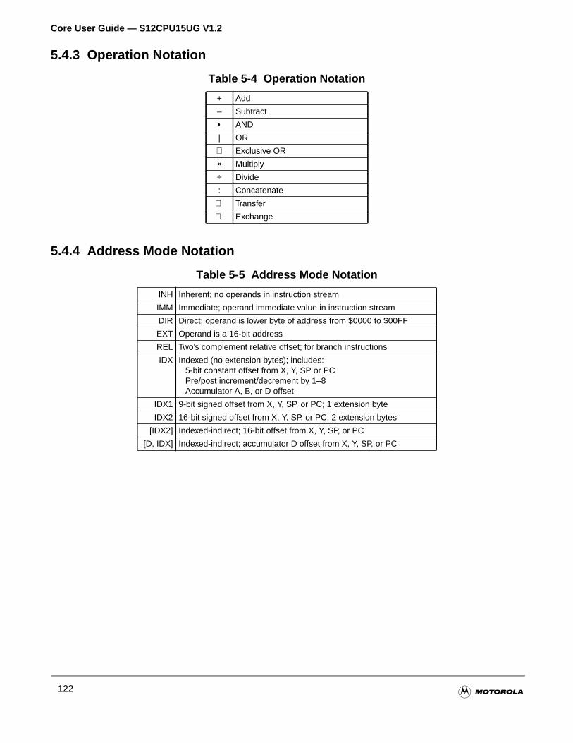
Core User Guide — S12CPU15UG V1.2
5.4.3 Operation Notation
5.4.4 Address Mode Notation
Table 5-4 Operation Notation
+ Add
– Subtract
• AND
| OR
⊕ Exclusive OR
× Multiply
÷ Divide
: Concatenate
⇒ Transfer
⇔ Exchange
Table 5-5 Address Mode Notation
INH Inherent; no operands in instruction stream
IMM Immediate; operand immediate value in instruction stream
DIR Direct; operand is lower byte of address from $0000 to $00FF
EXT Operand is a 16-bit address
REL Two’s complement relative offset; for branch instructions
IDX Indexed (no extension bytes); includes:5-bit constant offset from X, Y, SP or PCPre/post increment/decrement by 1–8Accumulator A, B, or D offset
IDX1 9-bit signed offset from X, Y, SP, or PC; 1 extension byte
IDX2 16-bit signed offset from X, Y, SP, or PC; 2 extension bytes
[IDX2] Indexed-indirect; 16-bit offset from X, Y, SP, or PC
[D, IDX] Indexed-indirect; accumulator D offset from X, Y, SP, or PC
122
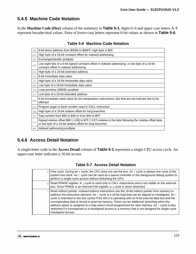
Core User Guide — S12CPU15UG V1.2
n
5.4.5 Machine Code Notation
In theMachine Code (Hex)column of the summary inTable 5-1 , digits 0–9 and upper case letters A–Frepresent hexadecimal values. Pairs of lower-case letters represent 8-bit values as shown inTable 5-6 .
5.4.6 Access Detail Notation
A single-letter code in theAccess Detailcolumn ofTable 5-1 represents a single CPU access cycle. Aupper-case letter indicates a 16-bit access.
Table 5-6 Machine Code Notation
dd 8-bit direct address from $0000 to $00FF; high byte is $00
ee High byte of a 16-bit constant offset for indexed addressing
eb Exchange/transfer postbyte
ffLow eight bits of a 9-bit signed constant offset in indexed addressing, or low byte of a 16-bitconstant offset in indexed addressing
hh High byte of a 16-bit extended address
ii 8-bit immediate data value
jj High byte of a 16-bit immediate data value
kk Low byte of a 16-bit immediate data value
lb Loop primitive (DBNE) postbyte
ll Low byte of a 16-bit extended address
mm8-bit immediate mask value for bit manipulation instructions; bits that are set indicate bits to beaffected
pg Program page or bank number used in CALL instruction
qq High byte of a 16-bit relative offset for long branches
tn Trap number from $30 to $39 or from $40 to $FF
rrSigned relative offset $80 (–128) to $7F (+127) relative to the byte following the relative offset byte,or low byte of a 16-bit relative offset for long branches
xb Indexed addressing postbyte
Table 5-7 Access Detail Notation
f Free cycle. During an f cycle, the CPU does not use the bus. An f cycle is always one cycle of thesystem bus clock. An f cycle can be used by a queue controller or the background debug system toperform a single-cycle access without disturbing the CPU.
g Read PPAGE register. A g cycle is used only in CALL instructions and is not visible on the externalbus. Since PPAGE is an internal 8-bit register, a g cycle is never stretched.
I Read indirect pointer. Indexed-indirect instructions use the 16-bit indirect pointer from memory toaddress the instruction operand. An I cycle is a 16-bit read that can be aligned or misaligned. An Icycle is extended to two bus cycles if the MCU is operating with an 8-bit external data bus and thecorresponding data is stored in external memory. There can be additional stretching when theaddress space is assigned to a chip-select circuit programmed for slow memory. An I cycle is alsostretched if it corresponds to a misaligned access to a memory that is not designed for single-cyclemisaligned access.
123
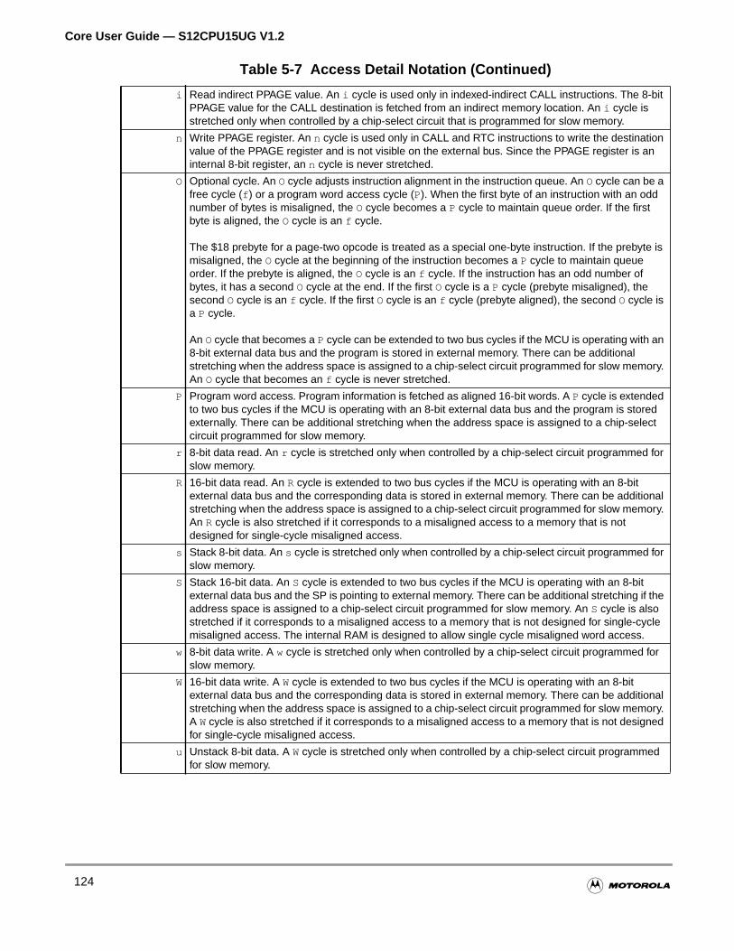
Core User Guide — S12CPU15UG V1.2
i Read indirect PPAGE value. An i cycle is used only in indexed-indirect CALL instructions. The 8-bitPPAGE value for the CALL destination is fetched from an indirect memory location. An i cycle isstretched only when controlled by a chip-select circuit that is programmed for slow memory.
n Write PPAGE register. An n cycle is used only in CALL and RTC instructions to write the destinationvalue of the PPAGE register and is not visible on the external bus. Since the PPAGE register is aninternal 8-bit register, an n cycle is never stretched.
O Optional cycle. An Ocycle adjusts instruction alignment in the instruction queue. An Ocycle can be afree cycle (f ) or a program word access cycle (P). When the first byte of an instruction with an oddnumber of bytes is misaligned, the O cycle becomes a P cycle to maintain queue order. If the firstbyte is aligned, the O cycle is an f cycle.
The $18 prebyte for a page-two opcode is treated as a special one-byte instruction. If the prebyte ismisaligned, the O cycle at the beginning of the instruction becomes a P cycle to maintain queueorder. If the prebyte is aligned, the O cycle is an f cycle. If the instruction has an odd number ofbytes, it has a second O cycle at the end. If the first O cycle is a P cycle (prebyte misaligned), thesecond Ocycle is an f cycle. If the first Ocycle is an f cycle (prebyte aligned), the second Ocycle isa P cycle.
An Ocycle that becomes a P cycle can be extended to two bus cycles if the MCU is operating with an8-bit external data bus and the program is stored in external memory. There can be additionalstretching when the address space is assigned to a chip-select circuit programmed for slow memory.An O cycle that becomes an f cycle is never stretched.
P Program word access. Program information is fetched as aligned 16-bit words. A P cycle is extendedto two bus cycles if the MCU is operating with an 8-bit external data bus and the program is storedexternally. There can be additional stretching when the address space is assigned to a chip-selectcircuit programmed for slow memory.
r 8-bit data read. An r cycle is stretched only when controlled by a chip-select circuit programmed forslow memory.
R 16-bit data read. An R cycle is extended to two bus cycles if the MCU is operating with an 8-bitexternal data bus and the corresponding data is stored in external memory. There can be additionalstretching when the address space is assigned to a chip-select circuit programmed for slow memory.An R cycle is also stretched if it corresponds to a misaligned access to a memory that is notdesigned for single-cycle misaligned access.
s Stack 8-bit data. An s cycle is stretched only when controlled by a chip-select circuit programmed forslow memory.
S Stack 16-bit data. An S cycle is extended to two bus cycles if the MCU is operating with an 8-bitexternal data bus and the SP is pointing to external memory. There can be additional stretching if theaddress space is assigned to a chip-select circuit programmed for slow memory. An S cycle is alsostretched if it corresponds to a misaligned access to a memory that is not designed for single-cyclemisaligned access. The internal RAM is designed to allow single cycle misaligned word access.
w 8-bit data write. A w cycle is stretched only when controlled by a chip-select circuit programmed forslow memory.
W 16-bit data write. A W cycle is extended to two bus cycles if the MCU is operating with an 8-bitexternal data bus and the corresponding data is stored in external memory. There can be additionalstretching when the address space is assigned to a chip-select circuit programmed for slow memory.A Wcycle is also stretched if it corresponds to a misaligned access to a memory that is not designedfor single-cycle misaligned access.
u Unstack 8-bit data. A W cycle is stretched only when controlled by a chip-select circuit programmedfor slow memory.
Table 5-7 Access Detail Notation (Continued)
124
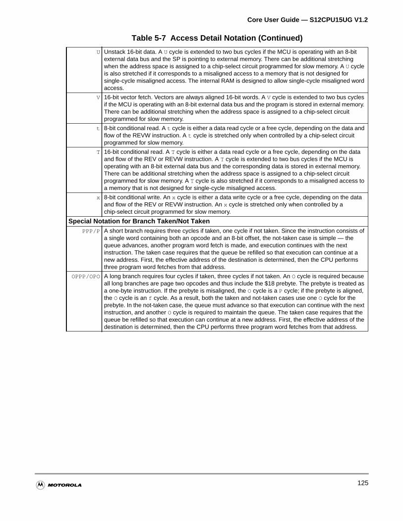
Core User Guide — S12CPU15UG V1.2
U Unstack 16-bit data. A U cycle is extended to two bus cycles if the MCU is operating with an 8-bitexternal data bus and the SP is pointing to external memory. There can be additional stretchingwhen the address space is assigned to a chip-select circuit programmed for slow memory. A U cycleis also stretched if it corresponds to a misaligned access to a memory that is not designed forsingle-cycle misaligned access. The internal RAM is designed to allow single-cycle misaligned wordaccess.
V 16-bit vector fetch. Vectors are always aligned 16-bit words. A V cycle is extended to two bus cyclesif the MCU is operating with an 8-bit external data bus and the program is stored in external memory.There can be additional stretching when the address space is assigned to a chip-select circuitprogrammed for slow memory.
t 8-bit conditional read. A t cycle is either a data read cycle or a free cycle, depending on the data andflow of the REVW instruction. A t cycle is stretched only when controlled by a chip-select circuitprogrammed for slow memory.
T 16-bit conditional read. A T cycle is either a data read cycle or a free cycle, depending on the dataand flow of the REV or REVW instruction. A T cycle is extended to two bus cycles if the MCU isoperating with an 8-bit external data bus and the corresponding data is stored in external memory.There can be additional stretching when the address space is assigned to a chip-select circuitprogrammed for slow memory. A T cycle is also stretched if it corresponds to a misaligned access toa memory that is not designed for single-cycle misaligned access.
x 8-bit conditional write. An x cycle is either a data write cycle or a free cycle, depending on the dataand flow of the REV or REVW instruction. An x cycle is stretched only when controlled by achip-select circuit programmed for slow memory.
Special Notation for Branch Taken/Not TakenPPP/P A short branch requires three cycles if taken, one cycle if not taken. Since the instruction consists of
a single word containing both an opcode and an 8-bit offset, the not-taken case is simple — thequeue advances, another program word fetch is made, and execution continues with the nextinstruction. The taken case requires that the queue be refilled so that execution can continue at anew address. First, the effective address of the destination is determined, then the CPU performsthree program word fetches from that address.
OPPP/OPO A long branch requires four cycles if taken, three cycles if not taken. An O cycle is required becauseall long branches are page two opcodes and thus include the $18 prebyte. The prebyte is treated asa one-byte instruction. If the prebyte is misaligned, the O cycle is a P cycle; if the prebyte is aligned,the O cycle is an f cycle. As a result, both the taken and not-taken cases use one O cycle for theprebyte. In the not-taken case, the queue must advance so that execution can continue with the nextinstruction, and another O cycle is required to maintain the queue. The taken case requires that thequeue be refilled so that execution can continue at a new address. First, the effective address of thedestination is determined, then the CPU performs three program word fetches from that address.
Table 5-7 Access Detail Notation (Continued)
125
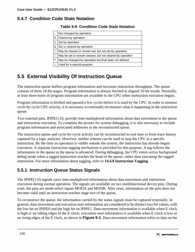
Core User Guide — S12CPU15UG V1.2
ueally,
egins.
onitorction
ueueclude
istory
unegroundtagged
urings not
ly. Ins, withlockw ore
5.4.7 Condition Code State Notation
5.5 External Visibility Of Instruction Queue
The instruction queue buffers program information and increases instruction throughput. The queconsists of three 16-bit stages. Program information is always fetched in aligned 16-bit words. Normat least three bytes of program information are available to the CPU when instruction execution b
Program information is fetched and queued a few cycles before it is used by the CPU. In order to mcycle-by-cycle CPU activity, it is necessary to externally reconstruct what is happening in the instruqueue.
Two external pins, IPIPE[1:0], provide time-multiplexed information about data movement in the qand instruction execution. To complete the picture for system debugging, it is also necessary to inprogram information and associated addresses in the reconstructed queue.
The instruction queue and cycle-by-cycle activity can be reconstructed in real time or from trace hcaptured by a logic analyzer. However, neither scheme can be used to stop the CPU at a specificinstruction. By the time an operation is visible outside the system, the instruction has already begexecution. A separate instruction tagging mechanism is provided for this purpose. A tag follows thinformation in the queue as the queue is advanced. During debugging, the CPU enters active backdebug mode when a tagged instruction reaches the head of the queue, rather than executing the instruction. For more information about tagging, refer to14.4.8 Instruction Tagging.
5.5.1 Instruction Queue Status Signals
The IPIPE[1:0] signals carry time-multiplexed information about data movement and instructionexecution during normal operation. The signals are available on two multifunctional device pins. Dreset, the pins are mode-select inputs MODA and MODB. After reset, information on the pins doebecome valid until an instruction reaches stage two of the queue.
To reconstruct the queue, the information carried by the status signals must be captured externalgeneral, data-movement and execution-start information are considered to be distinct two-bit valuethe low bit on IPIPE0 and the high bit on IPIPE1. Data-movement information is available when E cis high or on falling edges of the E clock; execution-start information is available when E clock is loon rising edges of the E clock, as shown inFigure 5-1 . Data-movement information refers to data on th
Table 5-8 Condition Code State Notation
– Not changed by operation
0 Cleared by operation
1 Set by operation
∆ Set or cleared by operation
⇓ May be cleared or remain set, but not set by operation
⇑ May be set or remain cleared, but not cleared by operation
? May be changed by operation but final state not defined
! Used for a special purpose
126
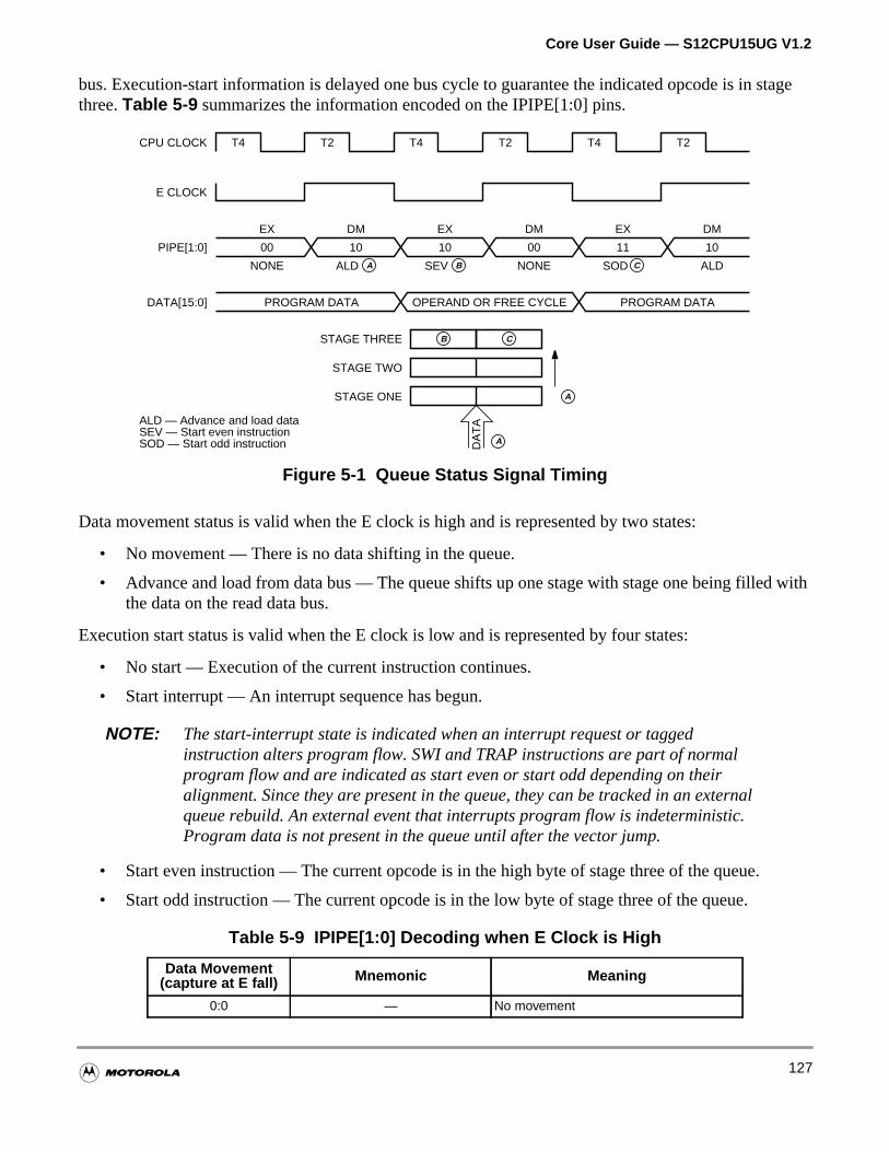
Core User Guide — S12CPU15UG V1.2
stage
with
bus. Execution-start information is delayed one bus cycle to guarantee the indicated opcode is in three.Table 5-9 summarizes the information encoded on the IPIPE[1:0] pins.
Figure 5-1 Queue Status Signal Timing
Data movement status is valid when the E clock is high and is represented by two states:
• No movement — There is no data shifting in the queue.
• Advance and load from data bus — The queue shifts up one stage with stage one being filledthe data on the read data bus.
Execution start status is valid when the E clock is low and is represented by four states:
• No start — Execution of the current instruction continues.
• Start interrupt — An interrupt sequence has begun.
NOTE: The start-interrupt state is indicated when an interrupt request or taggedinstruction alters program flow. SWI and TRAP instructions are part of normalprogram flow and are indicated as start even or start odd depending on theiralignment. Since they are present in the queue, they can be tracked in an externalqueue rebuild. An external event that interrupts program flow is indeterministic.Program data is not present in the queue until after the vector jump.
• Start even instruction — The current opcode is in the high byte of stage three of the queue.
• Start odd instruction — The current opcode is in the low byte of stage three of the queue.
Table 5-9 IPIPE[1:0] Decoding when E Clock is High
Data Movement(capture at E fall) Mnemonic Meaning
0:0 — No movement
CPU CLOCK
E CLOCK
DATA[15:0]
T2 T4 T2 T4T4 T2
EX EX EXDMDM
PIPE[1:0]
NONE SEV SODNONEALD
PROGRAM DATA OPERAND OR FREE CYCLE PROGRAM DATA
DM
ALD
STAGE THREE
STAGE TWO
STAGE ONE A
A B
B
C
C
ADA
TA
00 10 110010 10
ALD — Advance and load dataSEV — Start even instructionSOD — Start odd instruction
127
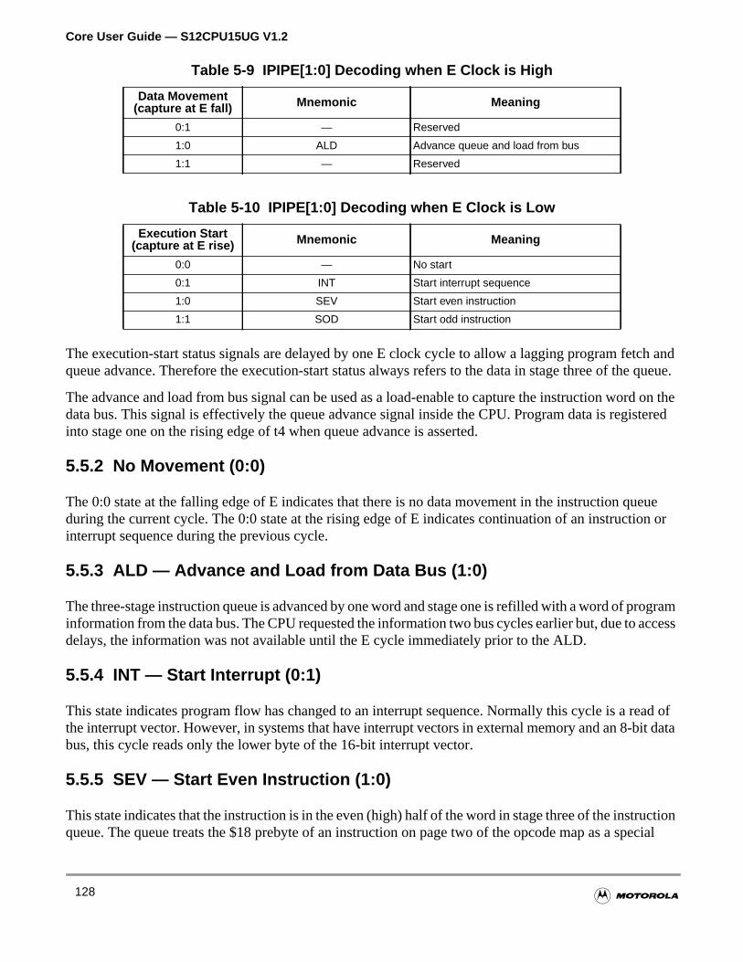
Core User Guide — S12CPU15UG V1.2
tch ande queue.
on theistered
eueon or
ogramaccess
ead ofit data
ctionecial
The execution-start status signals are delayed by one E clock cycle to allow a lagging program fequeue advance. Therefore the execution-start status always refers to the data in stage three of th
The advance and load from bus signal can be used as a load-enable to capture the instruction worddata bus. This signal is effectively the queue advance signal inside the CPU. Program data is reginto stage one on the rising edge of t4 when queue advance is asserted.
5.5.2 No Movement (0:0)
The 0:0 state at the falling edge of E indicates that there is no data movement in the instruction quduring the current cycle. The 0:0 state at the rising edge of E indicates continuation of an instructiinterrupt sequence during the previous cycle.
5.5.3 ALD — Advance and Load from Data Bus (1:0)
The three-stage instruction queue is advanced by one word and stage one is refilled with a word of prinformation from the data bus. The CPU requested the information two bus cycles earlier but, due todelays, the information was not available until the E cycle immediately prior to the ALD.
5.5.4 INT — Start Interrupt (0:1)
This state indicates program flow has changed to an interrupt sequence. Normally this cycle is a rthe interrupt vector. However, in systems that have interrupt vectors in external memory and an 8-bbus, this cycle reads only the lower byte of the 16-bit interrupt vector.
5.5.5 SEV — Start Even Instruction (1:0)
This state indicates that the instruction is in the even (high) half of the word in stage three of the instruqueue. The queue treats the $18 prebyte of an instruction on page two of the opcode map as a sp
0:1 — Reserved
1:0 ALD Advance queue and load from bus
1:1 — Reserved
Table 5-10 IPIPE[1:0] Decoding when E Clock is Low
Execution Start(capture at E rise) Mnemonic Meaning
0:0 — No start
0:1 INT Start interrupt sequence
1:0 SEV Start even instruction
1:1 SOD Start odd instruction
Table 5-9 IPIPE[1:0] Decoding when E Clock is High
Data Movement(capture at E fall) Mnemonic Meaning
128
Core User Guide — S12CPU15UG V1.2
the
ctionecial
the
one-byte, one-cycle instruction. However, interrupts are not recognized at the boundary between prebyte and the rest of the instruction.
5.5.6 SOD — Start Odd Instruction (1:1)
This state indicates that the instruction in the odd (low) half of the word in stage three of the instruqueue. The queue treats the $18 prebyte of an instruction on page two of the opcode map as a spone-byte, one-cycle instruction. However, interrupts are not recognized at the boundary between prebyte and the rest of the instruction.
129

Core User Guide — S12CPU15UG V1.2
130

Core User Guide — S12CPU15UG V1.2
scribes
ests.tion
ddresss not
storedh
the
Section 6 Exception Processing
Exceptions are events that require a change in the sequence of instruction execution. This section dethe exceptions supported by the Core and their functionality.
6.1 Exception Processing Overview
The Core supports two basic types of exceptions; those from resets and those from interrupt requRegardless of the source, the first cycle in exception processing is a vector fetch cycle. The excepprocessing flow is shown inFigure 6-1 below. Relevant points within the flow are detailed in theparagraphs that follow.
During the vector fetch cycle, the CPU indicates to the system that it is requesting that the vector aof the pending exception having the highest priority be driven onto the address bus. The CPU doeprovide this address.
The vector points to the address where the exception service routine begins. Exception vectors arein a table at the top of the memory map ($FFB6–$FFFF). The CPU begins using the vector to fetcinstructions in the third cycle of the exception processing sequence.
After the vector fetch, the CPU selects one of the three processing paths based on the source of exception:
• Reset
• X bit maskable and I bit maskable interrupt request
• SWI and TRAP
1.0-V
131
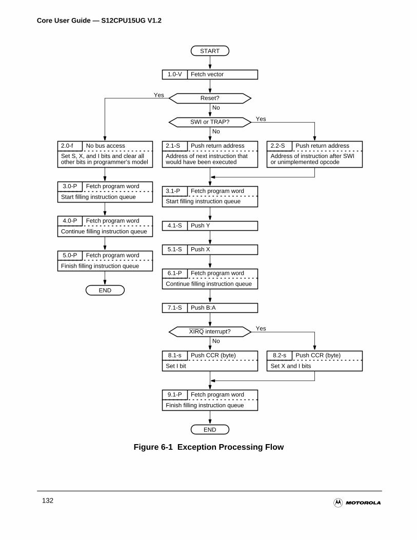
Core User Guide — S12CPU15UG V1.2
Figure 6-1 Exception Processing Flow
2.0-f No bus access
Set S, X, and I bits and clear allother bits in programmer’s model
5.0-P Fetch program word
Finish filling instruction queue
4.1-S Push Y
3.0-P Fetch program word
Start filling instruction queue
4.0-P Fetch program word
Continue filling instruction queue
2.1-S Push return address
Address of next instruction that
3.1-P Fetch program word
Start filling instruction queue
5.1-S Push X
6.1-P Fetch program word
Continue filling instruction queue
7.1-S Push B:A
XIRQ interrupt?
8.1-s Push CCR (byte)
Set I bit
END
SWI or TRAP?
START
1.0-V Fetch vector
Reset?
would have been executed
No
Yes
2.2-S Push return address
Address of instruction after SWIor unimplemented opcode
9.1-P Fetch program word
Finish filling instruction queue
8.2-s Push CCR (byte)
Set X and I bits
Yes
No
END
Yes
No
132
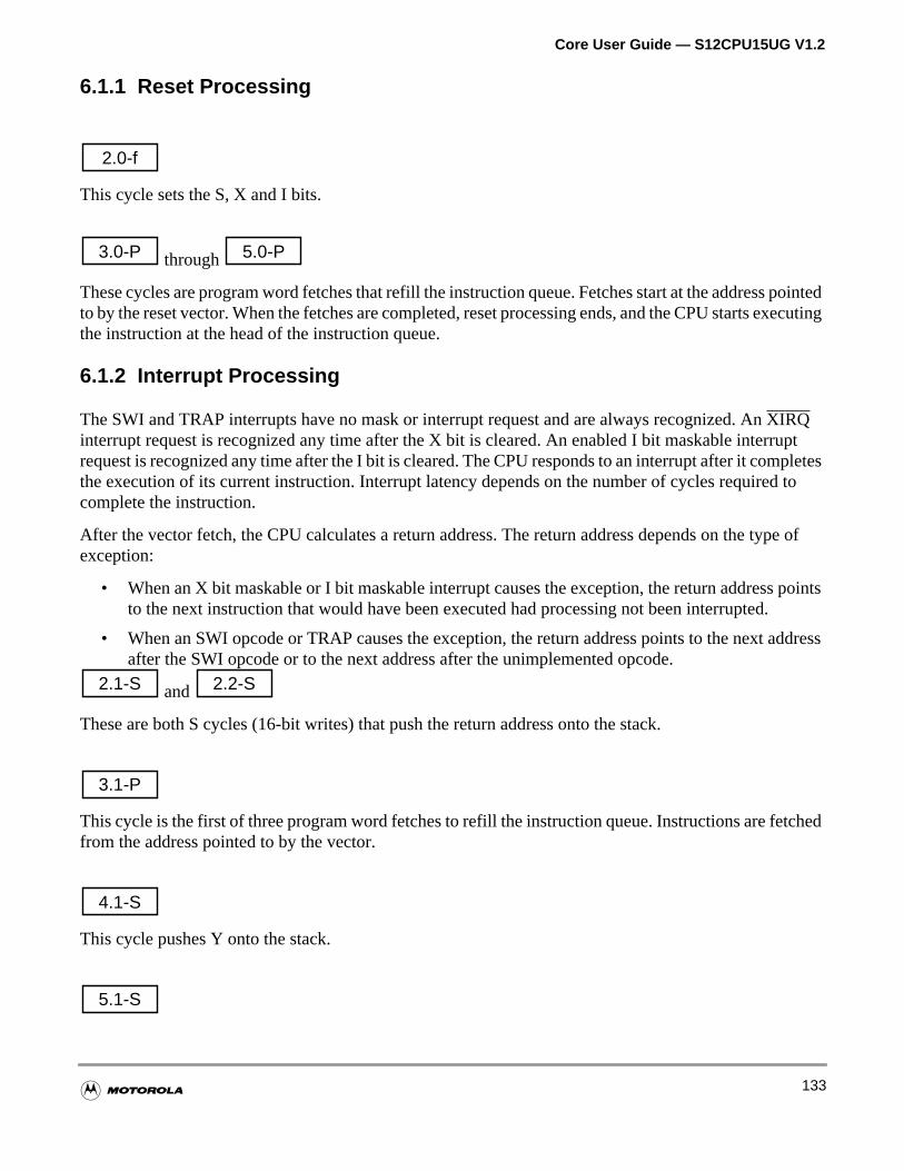
Core User Guide — S12CPU15UG V1.2
pointedxecuting
uptpletes to
pe of
points
ddress
ched
6.1.1 Reset Processing
This cycle sets the S, X and I bits.
through
These cycles are program word fetches that refill the instruction queue. Fetches start at the addressto by the reset vector. When the fetches are completed, reset processing ends, and the CPU starts ethe instruction at the head of the instruction queue.
6.1.2 Interrupt Processing
The SWI and TRAP interrupts have no mask or interrupt request and are always recognized. AnXIRQinterrupt request is recognized any time after the X bit is cleared. An enabled I bit maskable interrrequest is recognized any time after the I bit is cleared. The CPU responds to an interrupt after it comthe execution of its current instruction. Interrupt latency depends on the number of cycles requiredcomplete the instruction.
After the vector fetch, the CPU calculates a return address. The return address depends on the tyexception:
• When an X bit maskable or I bit maskable interrupt causes the exception, the return addressto the next instruction that would have been executed had processing not been interrupted.
• When an SWI opcode or TRAP causes the exception, the return address points to the next aafter the SWI opcode or to the next address after the unimplemented opcode.
and
These are both S cycles (16-bit writes) that push the return address onto the stack.
This cycle is the first of three program word fetches to refill the instruction queue. Instructions are fetfrom the address pointed to by the vector.
This cycle pushes Y onto the stack.
2.0-f
3.0-P 5.0-P
2.1-S 2.2-S
3.1-P
4.1-S
5.1-S
133
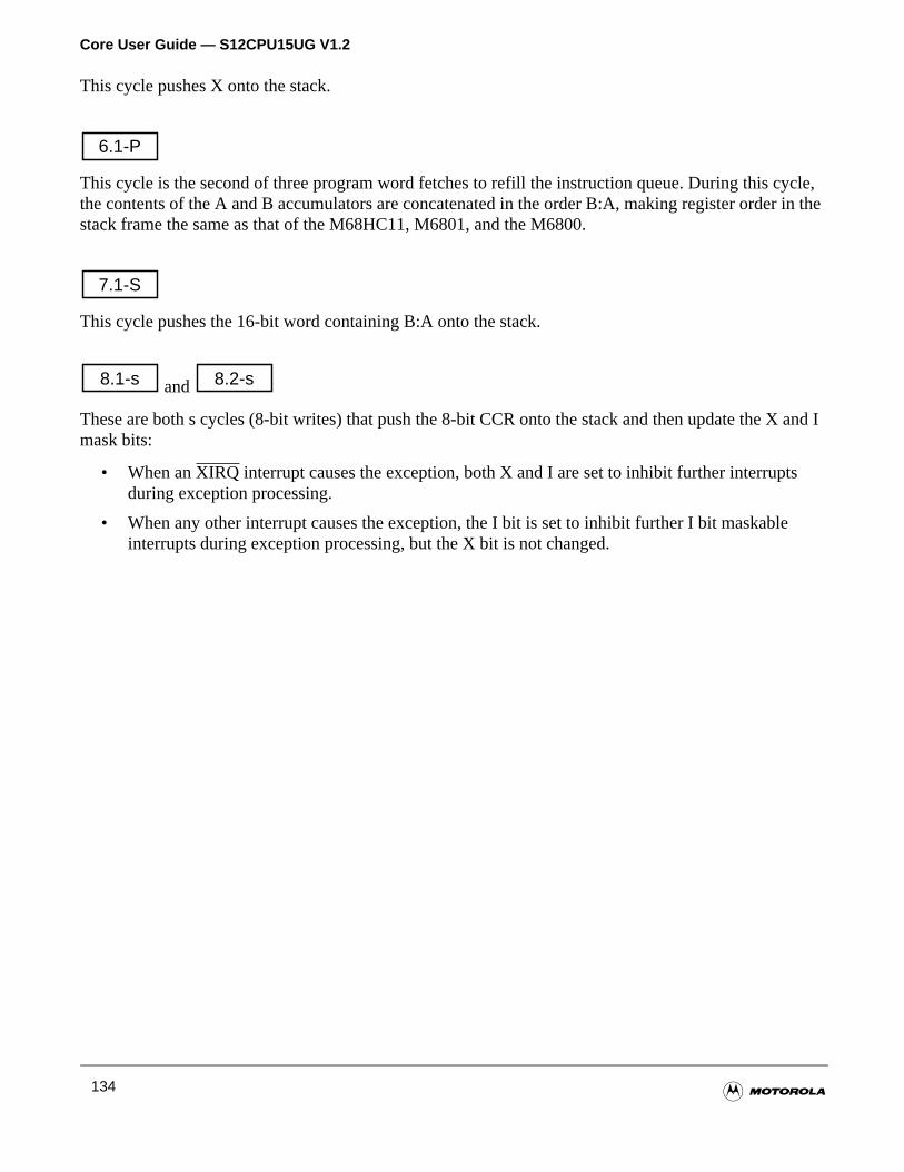
Core User Guide — S12CPU15UG V1.2
ycle,in the
X and I
s
e
This cycle pushes X onto the stack.
This cycle is the second of three program word fetches to refill the instruction queue. During this cthe contents of the A and B accumulators are concatenated in the order B:A, making register orderstack frame the same as that of the M68HC11, M6801, and the M6800.
This cycle pushes the 16-bit word containing B:A onto the stack.
and
These are both s cycles (8-bit writes) that push the 8-bit CCR onto the stack and then update the mask bits:
• When anXIRQ interrupt causes the exception, both X and I are set to inhibit further interruptduring exception processing.
• When any other interrupt causes the exception, the I bit is set to inhibit further I bit maskablinterrupts during exception processing, but the X bit is not changed.
6.1-P
7.1-S
8.1-s 8.2-s
134
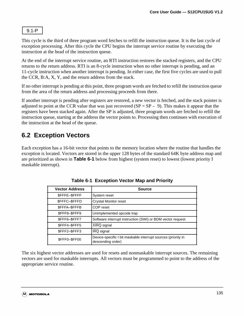
Core User Guide — S12CPU15UG V1.2
le ofe
e CPU ano pull
ueue
inter ishat theefill theution of
les theap and
aining of the
This cycle is the third of three program word fetches to refill the instruction queue. It is the last cycexception processing. After this cycle the CPU begins the interrupt service routine by executing thinstruction at the head of the instruction queue.
At the end of the interrupt service routine, an RTI instruction restores the stacked registers, and threturns to the return address. RTI is an 8-cycle instruction when no other interrupt is pending, and11-cycle instruction when another interrupt is pending. In either case, the first five cycles are used tthe CCR, B:A, X, Y, and the return address from the stack.
If no other interrupt is pending at this point, three program words are fetched to refill the instruction qfrom the area of the return address and processing proceeds from there.
If another interrupt is pending after registers are restored, a new vector is fetched, and the stack poadjusted to point at the CCR value that was just recovered (SP = SP – 9). This makes it appear tregisters have been stacked again. After the SP is adjusted, three program words are fetched to rinstruction queue, starting at the address the vector points to. Processing then continues with execthe instruction at the head of the queue.
6.2 Exception Vectors
Each exception has a 16-bit vector that points to the memory location where the routine that handexception is located. Vectors are stored in the upper 128 bytes of the standard 64K byte address mare prioritized as shown inTable 6-1 below from highest (system reset) to lowest (lowest priority Imaskable interrupt).
The six highest vector addresses are used for resets and nonmaskable interrupt sources. The remvectors are used for maskable interrupts. All vectors must be programmed to point to the addressappropriate service routine.
Table 6-1 Exception Vector Map and Priority
Vector Address Source
$FFFE–$FFFF System reset
$FFFC–$FFFD Crystal Monitor reset
$FFFA–$FFFB COP reset
$FFF8–$FFF9 Unimplemented opcode trap
$FFF6–$FFF7 Software interrupt instruction (SWI) or BDM vector request
$FFF4–$FFF5 XIRQ signal
$FFF2–$FFF3 IRQ signal
$FFF0–$FF00Device-specific I bit maskable interrupt sources (priority indescending order)
9.1-P
135
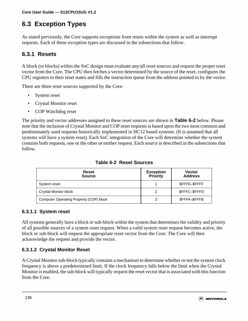
Core User Guide — S12CPU15UG V1.2
upt
r resetres thevector.
on andt all
ystemions that
ioritytive, the
clockstalction
6.3 Exception Types
As stated previously, the Core supports exceptions from resets within the system as well as interrrequests. Each of these exception types are discussed in the subsections that follow.
6.3.1 Resets
A block (or blocks) within the SoC design must evaluate any/all reset sources and request the propevector from the Core. The CPU then fetches a vector determined by the source of the reset, configuCPU registers to their reset states and fills the instruction queue from the address pointed to by the
There are three reset sources supported by the Core:
• System reset
• Crystal Monitor reset
• COP Watchdog reset
The priority and vector addresses assigned to these reset sources are shown inTable 6-2 below. Pleasenote that the inclusion of Crystal Monitor and COP reset requests is based upon the two most commpredominately used requests historically implemented in HC12 based systems. (It is assumed thasystems will have a system reset). Each SoC integration of the Core will determine whether the scontains both requests, one or the other or neither request. Each source is described in the subsectfollow.
6.3.1.1 System reset
All systems generally have a block or sub-block within the system that determines the validity and prof all possible sources of a system reset request. When a valid system reset request becomes acblock or sub-block will request the appropriate reset vector from the Core. The Core will thenacknowledge the request and provide the vector.
6.3.1.2 Crystal Monitor Reset
A Crystal Monitor sub-block typically contains a mechanism to determine whether or not the systemfrequency is above a predetermined limit. If the clock frequency falls below the limit when the CryMonitor is enabled, the sub-block will typically request the reset vector that is associated with this funfrom the Core.
Table 6-2 Reset Sources
ResetSource
ExceptionPriority
VectorAddress
System reset 1 $FFFE–$FFFF
Crystal Monitor block 2 $FFFC–$FFFD
Computer Operating Properly (COP) block 3 $FFFA–$FFFB
136
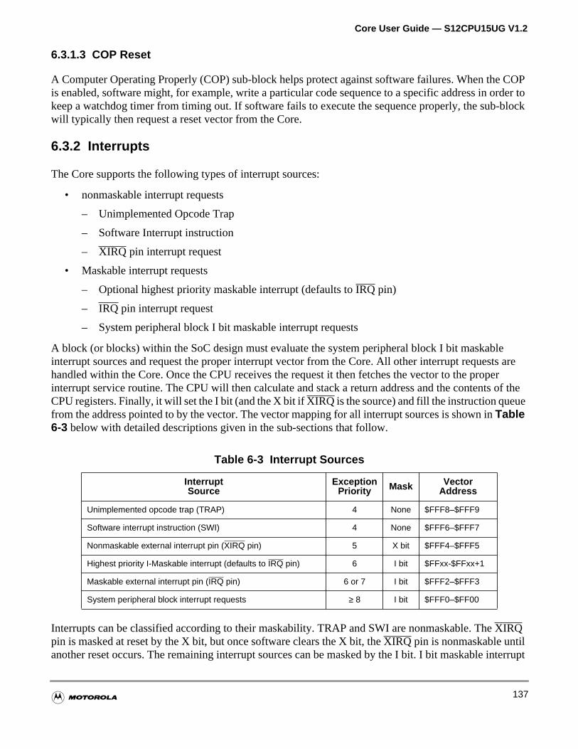
Core User Guide — S12CPU15UG V1.2
COPrder toblock
les areer of the
terrupt
6.3.1.3 COP Reset
A Computer Operating Properly (COP) sub-block helps protect against software failures. When theis enabled, software might, for example, write a particular code sequence to a specific address in okeep a watchdog timer from timing out. If software fails to execute the sequence properly, the sub-will typically then request a reset vector from the Core.
6.3.2 Interrupts
The Core supports the following types of interrupt sources:
• nonmaskable interrupt requests
– Unimplemented Opcode Trap
– Software Interrupt instruction
– XIRQ pin interrupt request
• Maskable interrupt requests
– Optional highest priority maskable interrupt (defaults toIRQ pin)
– IRQ pin interrupt request
– System peripheral block I bit maskable interrupt requests
A block (or blocks) within the SoC design must evaluate the system peripheral block I bit maskabinterrupt sources and request the proper interrupt vector from the Core. All other interrupt requesthandled within the Core. Once the CPU receives the request it then fetches the vector to the propinterrupt service routine. The CPU will then calculate and stack a return address and the contentsCPU registers. Finally, it will set the I bit (and the X bit ifXIRQ is the source) and fill the instruction queuefrom the address pointed to by the vector. The vector mapping for all interrupt sources is shown inTable6-3 below with detailed descriptions given in the sub-sections that follow.
Interrupts can be classified according to their maskability. TRAP and SWI are nonmaskable. TheXIRQpin is masked at reset by the X bit, but once software clears the X bit, theXIRQ pin is nonmaskable untilanother reset occurs. The remaining interrupt sources can be masked by the I bit. I bit maskable in
Table 6-3 Interrupt Sources
InterruptSource
ExceptionPriority Mask Vector
Address
Unimplemented opcode trap (TRAP) 4 None $FFF8–$FFF9
Software interrupt instruction (SWI) 4 None $FFF6–$FFF7
Nonmaskable external interrupt pin (XIRQ pin) 5 X bit $FFF4–$FFF5
Highest priority I-Maskable interrupt (defaults to IRQ pin) 6 I bit $FFxx-$FFxx+1
Maskable external interrupt pin (IRQ pin) 6 or 7 I bit $FFF2–$FFF3
System peripheral block interrupt requests ≥ 8 I bit $FFF0–$FF00
137
Core User Guide — S12CPU15UG V1.2
orts.ctors:
otherion for
he 202unused
APstate.
differsturncode for
servicee.
bit.
ared,
otherres
ing therrupt
requests come from theIRQ pin and peripheral blocks within the system such as timers and serial pThese I bit maskable sources have default priorities that follow the address order of the interrupt vethe higher the address, the higher the priority of the interrupt request. TheIRQ pin is initially assigned thehighest I bit maskable interrupt priority. The system can give one I bit maskable source priority overI bit maskable sources configured at integration of the Core into the SoC design. The documentateach system should provide more information.
6.3.2.1 Unimplemented Opcode Trap (TRAP)
Only 54 of the 256 positions on page 2 of the opcode map are used. Attempting to execute one of tunused opcodes on page 2 causes a nonmaskable interrupt without an interrupt request. All 202 opcodes share the same interrupt vector, $FFF8:$FFF9.
TRAP processing stacks the CCR and then sets the I bit to prevent other interrupts during the TRservice routine. An RTI instruction at the end of the service routine restores the I bit to its preinterrupt
The CPU uses the next address after an unimplemented page 2 opcode as a return address. Thisfrom the M68HC11 illegal opcode interrupt, which uses the address of an illegal opcode as the readdress. The stacked return address can be used to calculate the address of the unimplemented opsoftware-controlled traps.
6.3.2.2 Software Interrupt Instruction (SWI)
Execution of the SWI instruction causes a nonmaskable interrupt without an interrupt request.
SWI processing stacks the CCR and then sets the I bit to prevent other interrupts during the SWI routine. An RTI instruction at the end of the service routine restores the I bit to its preinterrupt stat
NOTE: CPU processing of a TRAP or SWI cannot be interrupted. Also, TRAP and SWI aremutually exclusive instructions with no relative priority.
6.3.2.3 Nonmaskable External Interrupt Request Pin ( XIRQ)
Driving theXIRQ pin low generates an external interrupt request, subject initially to masking by the XReset sets the X bit, maskingXIRQ interrupt requests. Software can unmaskXIRQ interrupt requests onceafter reset by clearing the X bit with an instruction such as ANDCC #$BF. After the X bit has been cleit cannot be set andXIRQ interrupt requests are nonmaskable until another reset occurs.
XIRQ interrupt request processing stacks the CCR and then sets both the X and I bits to prevent interrupts during theXIRQ service routine. An RTI instruction at the end of the service routine restothe X and I bits to their preinterrupt states.
6.3.2.4 Maskable External Interrupt Request Pin ( IRQ)
Driving theIRQ pin low generates an external interrupt request, subject to masking by the I bit.IRQinterrupt request processing stacks the CCR and then sets the I bit to prevent other interrupts durIRQ service routine. An RTI instruction at the end of the service routine restores the I bit to its preintestate.
138
Core User Guide — S12CPU15UG V1.2
I bit.bit totine
le bitsuired
tional
The Interrupt sub-block of the Core (INT) also has a control bit to disconnect theIRQ input. Please seeSection 10 of this guide for a more detailed description.
6.3.2.5 System Peripheral Block Interrupt Requests
Some system peripheral blocks can generate interrupt requests that are subject to masking by theProcessing of an interrupt request from one of these sources stacks the CCR and then sets the I prevent other interrupts during the service routine. An RTI instruction at the end of the service rourestores the I bit to its preinterrupt state.
Interrupt requests from a system peripheral block may also be subject to masking by interrupt enabin control registers. In addition, there may be interrupt flags with register read-write sequences reqfor flag clearing. The documentation for the system peripheral block should provide a detailed funcdescription.
139

Core User Guide — S12CPU15UG V1.2
140
Core User Guide — S12CPU15UG V1.2
ed
terfaceheion to
p and logic
at aren-chip
Section 7 Core Interface
This section provides a brief description of the Core interface to the rest of the SoC design. Detailinformation on the Core interface, such as more complete descriptions of all signals and timinginformation, is provided in theHCS12 V1.5 Core Integration Guide.
7.1 Core Interface Overview
The Core is designed to be integrated into a SoC design as a fully synthesizable block. The Core inis shown inFigure 7-1 below with the interface signals grouped by function. All signals related to tinternal and I.P. bus interfacing appear on the right side of the Core block in the diagram. In additbus interfacing, the Core receives reset and clock inputs from the system and provides signals forinteracting with the CPU for vector request and acknowledge and for functional operation of the stowait modes. The Core interacts with the external blocks of the overall system through the port/padfor Ports A, B, E (which include the physicalIRQ andXIRQ pins) and K and the BDM BKGD pininterfaces. The memory configuration switches shown in the diagram are inputs to the Core block thtied to a constant logic state at the time of integration into the SoC design to correctly define the omemory configuration for proper Core operation within the system.
141
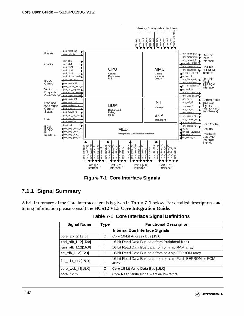
Core User Guide — S12CPU15UG V1.2
.
Figure 7-1 Core Interface Signals
7.1.1 Signal Summary
A brief summary of the Core interface signals is given inTable 7-1 below. For detailed descriptions andtiming information please consult theHCS12 V1.5 Core Integration Guide.
Table 7-1 Core Interface Signal Definitions
Signal Name Type Functional Description
Internal Bus Interface Signalscore_ab_t2[19:0] O Core 16-bit Address Bus [19:0]
peri_rdb_L12[15:0] I 16-bit Read Data Bus data from Peripheral block
ram_rdb_L12[15:0] I 16-bit Read Data Bus data from on-chip RAM array
ee_rdb_L12[15:0] I 16-bit Read Data Bus data from on-chip EEPROM array
fee_rdb_L12[15:0] I16-bit Read Data Bus data from on-chip Flash EEPROM or ROMarray
core_wdb_t4[15:0] O Core 16-bit Write Data Bus [15:0]
core_rw_t2 O Core Read/Write signal - active low Write
reset_pin_ind
peri_clk24
peri_clk23peri_clk34
peri_rdb_L12[15:0]peri_ffxx_t3peri_rtifff0i_t3
core_ramarraysel_t2
core_ab_t2[19:0]
core_wdb_t4[15:0]
core_rw_t2
core_sz8_t2
core_smod_t2
core_perisel_t2
core_bdmact_t4
ram_rdb_L12[15:0]
core_ramregsel_t2
core_eeregsel_t2
core_eearraysel_t2
ee_rdb_L12[15:0]
ee_hold_t1
core_feeregsel_t2
core_feearraysel_t2
fee_rdb_L12[15:0]
fee_hold_t1
core_secure_t2secreq
peri_reset_ta4
core_stop_t24
peri_phase_oscdX
peri_xmonv_request
peri_rstv_request
peri_copv_request
core_wakeup_tacore_wait_t24
peri_cwai_t3
peri_syswai_t3
peri_test_clk_enable
peri_pllsel_t3peri_test_clk
bkgd_ind
core_bkgd_obecore_bkgd_dout_t4
core_bkgd_ibe_t2core_bkgdpue_t2
core
_pai
nd[7
:0]
core
_pad
o[7:
0]
core
_pao
be[7
:0]
core
_pai
be_t
2
core
_pap
ue_t
2
core
_par
d_t2
core
_pei
nd[7
:0]
core
_ped
o[7:
0]
core
_peo
be[7
:0]
core
_pei
be_t
2
core
_pep
ue_t
2
core
_per
d_t2
core
_mdr
ste
core
_pbi
nd[7
:0]
core
_pbd
o[7:
0]
core
_pbo
be[7
:0]
core
_pbi
be_t
2
core
_pbp
ue_t
2
core
_pbr
d_t2
core
_pki
nd[7
:0]
core
_pkd
o[7:
0]
core
_pko
be[7
:0]
core
_pki
be_t
2
core
_pkp
ue_t
2
core
_pkr
d_t2
core
_xab
_t2
reg_
sw0
pag_
sw0
ram
_sw
2
ram
_sw
1
ram
_sw
0
eep_
sw1
eep_
sw0
rom
_sw
1
rom
_sw
0
rom
on_e
xp_s
tate
pag_
sw1
BDMBackgroundDebugMode
CPUCentralProcessingUnit
MMCModuleMappingControl
INTInterrupt
BKPBreakpoint
MEBIMultiplexed External Bus Interface
Port A[7:0]Interface
Port B[7:0]Interface
Port E[7:0]Interface
Port K[7:0]Interface
PeripheralBus OnlyInterfaceSignals
Security
Common BusInterfaceSignals(Memory andPeripherals)
On-Chip
On-ChipEEPROMInterface
On-ChipRAMInterface
Memory Configuration Switches
Resets
Clocks
VectorRequest/Acknowledge
Stop andWait ModeControl/Status
PLL
BDMBKGDPinInterface
FlashEEPROMInterface
core_eclk_load
core_neclk_t2
core_vector_fetch_t4
ECLKControl
core_ramhal_t2
ipt_scan_modeScan Control
core_exp_t2
ram
_fm
ts
peri_clk4
peri_clk2
core_per_t2
142
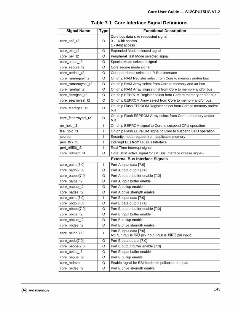
Core User Guide — S12CPU15UG V1.2
core_sz8_t2 OCore bus data size requested signal0 - 16-bit access1 - 8-bit access
core_exp_t2 O Expanded Mode selected signal
core_per_t2 O Peripheral Test Mode selected signal
core_smod_t2 O Special Mode selected signal
core_secure_t2 O Core secure mode signal
core_perisel_t2 O Core peripheral select to I.P. Bus Interface
core_ramregsel_t2 O On-chip RAM Register select from Core to memory and/or bus
core_ramarraysel_t2 O On-chip RAM Array select from Core to memory and /or bus
core_ramhal_t2 O On-chip RAM Array align signal from Core to memory and/or bus
core_eeregsel_t2 O On-chip EEPROM Register select from Core to memory and/or bus
core_eearraysel_t2 O On-chip EEPROM Array select from Core to memory and/or bus
core_feeregsel_t2 OOn-chip Flash EEPROM Register select from Core to memory and/orbus
core_feearraysel_t2 OOn-chip Flash EEPROM Array select from Core to memory and/orbus
ee_hold_t1 I On-chip EEPROM signal to Core to suspend CPU operation
fee_hold_t1 I On-chip Flash EEPROM signal to Core to suspend CPU operation
secreq I Security mode request from applicable memory
peri_ffxx_t3 I Interrupt Bus from I.P. Bus Interface
peri_rtifff0i_t3 I Real Time Interrupt signal
core_bdmact_t4 O Core BDM active signal for I.P. Bus Interface (freeze signal)
External Bus Interface Signalscore_paind[7:0] I Port A input data [7:0]
core_pado[7:0] O Port A data output [7:0]
core_paobe[7:0] O Port A output buffer enable [7:0]
core_paibe_t2 O Port A input buffer enable
core_papue_t2 O Port A pullup enable
core_padse_t2 O Port A drive strength enable
core_pbind[7:0] I Port B input data [7:0]
core_pbdo[7:0] O Port B data output [7:0]
core_pbobe[7:0] O Port B output buffer enable [7:0]
core_pbibe_t2 O Port B input buffer enable
core_pbpue_t2 O Port B pullup enable
core_pbdse_t2 O Port B drive strength enable
core_peind[7:0] IPort E input data [7:0]NOTE: PE1 is IRQ pin input; PE0 is XIRQ pin input.
core_pedo[7:0] O Port E data output [7:0]
core_peobe[7:0] O Port E output buffer enable [7:0]
core_peibe_t2 O Port E input buffer enable
core_pepue_t2 O Port E pullup enable
core_mdrste O Enable signal for EBI Mode pin pullups at the pad
core_pedse_t2 O Port E drive strength enable
Table 7-1 Core Interface Signal Definitions
Signal Name Type Functional Description
143
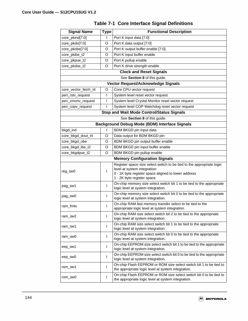
Core User Guide — S12CPU15UG V1.2
core_pkind[7:0] I Port K input data [7:0]
core_pkdo[7:0] O Port K data output [7:0]
core_pkobe[7:0] O Port K output buffer enable [7:0]
core_pkibe_t2 O Port K input buffer enable
core_pkpue_t2 O Port K pullup enable
core_pkdse_t2 O Port K drive strength enable
Clock and Reset SignalsSee Section 8 of this guide.
Vector Request/Acknowledge Signalscore_vector_fetch_t4 O Core CPU vector request
peri_rstv_request I System level reset vector request
peri_xmonv_request I System level Crystal Monitor reset vector request
peri_copv_request I System level COP Watchdog reset vector request
Stop and Wait Mode Control/Status SignalsSee Section 8 of this guide.
Background Debug Mode (BDM) Interface Signalsbkgd_ind I BDM BKGD pin input data
core_bkgd_dout_t4 O Data output for BDM BKGD pin
core_bkgd_obe O BDM BKGD pin output buffer enable
core_bkgd_ibe_t2 O BDM BKGD pin input buffer enable
core_bkgdpue_t2 O BDM BKGD pin pullup enable
Memory Configuration Signals
reg_sw0 I
Register space size select switch to be tied to the appropriate logiclevel at system integration:0 - 1K byte register space aligned to lower address1 - 2K byte register space.
pag_sw1 IOn-chip memory size select switch bit 1 to be tied to the appropriatelogic level at system integration.
pag_sw0 IOn-chip memory size select switch bit 0 to be tied to the appropriatelogic level at system integration.
ram_fmts IOn-chip RAM fast memory transfer select to be tied to theappropriate logic level at system integration.
ram_sw2 IOn-chip RAM size select switch bit 2 to be tied to the appropriatelogic level at system integration.
ram_sw1 IOn-chip RAM size select switch bit 1 to be tied to the appropriatelogic level at system integration.
ram_sw0 IOn-chip RAM size select switch bit 0 to be tied to the appropriatelogic level at system integration.
eep_sw1 IOn-chip EEPROM size select switch bit 1 to be tied to the appropriatelogic level at system integration.
eep_sw0 IOn-chip EEPROM size select switch bit 0 to be tied to the appropriatelogic level at system integration.
rom_sw1 IOn-chip Flash EEPROM or ROM size select switch bit 1 to be tied tothe appropriate logic level at system integration.
rom_sw0 IOn-chip Flash EEPROM or ROM size select switch bit 0 to be tied tothe appropriate logic level at system integration.
Table 7-1 Core Interface Signal Definitions
Signal Name Type Functional Description
144
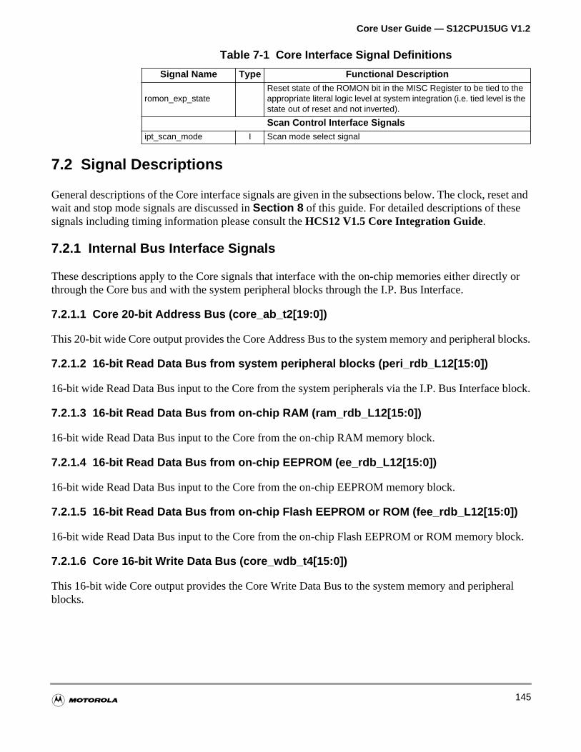
Core User Guide — S12CPU15UG V1.2
set and
tly or
locks.
block.
lock.
eral
7.2 Signal Descriptions
General descriptions of the Core interface signals are given in the subsections below. The clock, rewait and stop mode signals are discussed inSection 8 of this guide. For detailed descriptions of thesesignals including timing information please consult theHCS12 V1.5 Core Integration Guide.
7.2.1 Internal Bus Interface Signals
These descriptions apply to the Core signals that interface with the on-chip memories either directhrough the Core bus and with the system peripheral blocks through the I.P. Bus Interface.
7.2.1.1 Core 20-bit Address Bus (core_ab_t2[19:0])
This 20-bit wide Core output provides the Core Address Bus to the system memory and peripheral b
7.2.1.2 16-bit Read Data Bus from system peripheral blocks (peri_rdb_L12[15:0])
16-bit wide Read Data Bus input to the Core from the system peripherals via the I.P. Bus Interface
7.2.1.3 16-bit Read Data Bus from on-chip RAM (ram_rdb_L12[15:0])
16-bit wide Read Data Bus input to the Core from the on-chip RAM memory block.
7.2.1.4 16-bit Read Data Bus from on-chip EEPROM (ee_rdb_L12[15:0])
16-bit wide Read Data Bus input to the Core from the on-chip EEPROM memory block.
7.2.1.5 16-bit Read Data Bus from on-chip Flash EEPROM or ROM (fee_rdb_L12[15:0])
16-bit wide Read Data Bus input to the Core from the on-chip Flash EEPROM or ROM memory b
7.2.1.6 Core 16-bit Write Data Bus (core_wdb_t4[15:0])
This 16-bit wide Core output provides the Core Write Data Bus to the system memory and periphblocks.
romon_exp_stateReset state of the ROMON bit in the MISC Register to be tied to theappropriate literal logic level at system integration (i.e. tied level is thestate out of reset and not inverted).
Scan Control Interface Signalsipt_scan_mode I Scan mode select signal
Table 7-1 Core Interface Signal Definitions
Signal Name Type Functional Description
145
Core User Guide — S12CPU15UG V1.2
low)
eing
igured
u ise
red in
pace of
gister
array
7.2.1.7 Core Read/ Write signal (core_rw_t2)
This single bit Core output indicates the direction of bus access (read or write with write being activeby the Core.
7.2.1.8 Core bus data size request indicator (core_sz8_t2)
This single bit Core output indicates the size of data (8-bit or 16-bit when high or low, respectively) bread/written by a Core bus access.
7.2.1.9 Core Expanded Mode indicator (core_exp_t2)
This single bit Core output indicates that the Core is in Expanded Mode (i.e. the Core has been confin one of the expanded modes via the MODE pins)
7.2.1.10 Core Peripheral Test Mode indicator (core_per_t2)
This single bit Core output indicates that the Core is in Peripheral Test Mode. In this mode, the cpdisabled and the direction of the bus interface is switched such that the on-chip peripherals can baddressed directly. This mode is used for factory test only.
7.2.1.11 Core Special Mode indicator (core_smod_t2)
This single bit Core output indicates that the Core is in Special Mode (i.e. the Core has been configuSpecial Mode via the MODE pins)
7.2.1.12 Core Secure Mode indicator (core_secure_t2)
This single bit Core output indicates that the Core is operating in secured mode. Please seeSection 15of this guide for functional details.
7.2.1.13 Peripheral select signal (core_perisel_t2)
This single bit Core output indicates that the Core is accessing an address within the peripheral sthe system memory map.
7.2.1.14 On-Chip RAM register space select signal (core_ramregsel_t2)
This single bit Core output indicates that the Core is accessing an address within the on-chip RAM respace of the system memory map.
7.2.1.15 On-Chip RAM array select signal (core_ramarraysel_t2)
This single bit Core output indicates that the Core is accessing an address within the on-chip RAMspace of the system memory map.
146
Core User Guide — S12CPU15UG V1.2
ROM
ROM
h
h
of the
of the
e Core
stem
7.2.1.16 On-Chip RAM array align signal (core_ramhal_t2)
This single bit Core output reflects the state of the RAMHAL bit in the INITRAM register within theModule Mapping Control (MMC) sub-block of the Core. Please seeSection 11 of this guide for furtherfunctional details.
7.2.1.17 On-Chip EEPROM register select signal (core_eeregsel_t2)
This single bit Core output indicates that the Core is accessing an address within the on-chip EEPregister space of the system memory map.
7.2.1.18 On-Chip EEPROM array select signal (core_eearraysel_t2)
This single bit Core output indicates that the Core is accessing an address within the on-chip EEParray space of the system memory map.
7.2.1.19 On-Chip Flash EEPROM register select signal (core_feeregsel_t2)
This single bit Core output indicates that the Core is accessing an address within the on-chip FlasEEPROM register space of the system memory map.
7.2.1.20 On-Chip Flash EEPROM array select signal (core_feearraysel_t2)
This single bit Core output indicates that the Core is accessing an address within the on-chip FlasEEPROM array space of the system memory map.
7.2.1.21 On-Chip EEPROM hold signal to Core (ee_hold_t1)
This single bit input to the Core is used to suspend operation of the CPU when needed for functionson-chip EEPROM memory block.
7.2.1.22 On-Chip Flash EEPROM hold signal to Core (fee_hold_t1)
This single bit input to the Core is used to suspend operation of the CPU when needed for functionson-chip Flash EEPROM memory block.
7.2.1.23 Core Security Request (secreq)
This single bit input indicates to the Core that the system memory is in a secured state and that thshould operate in secured mode. Please seeSection 15 for functional details.
7.2.1.24 56-bit Interrupt request signals from peripheral block to Core (peri_ffxx_t3)
This 56-bit wide input to the Core provides the Core with the Interrupt request signals from all the syinterrupt sources via the I.P. Bus Interface.
147
Core User Guide — S12CPU15UG V1.2
Time
terfacee.
ic for
Port
m
logic
ic for
ed
ic for
7.2.1.25 System Real Time Interrupt request (peri_rtifff0i_t3)
This input signal indicates to the Core that the system is requesting the interrupt vector for a RealInterrupt (RTI) from the Core.
7.2.1.26 Background Debug Mode active indicator (core_bdmact_t4)
This single bit output from the Core indicates that the Background Debug Mode (BDM) is active.
7.2.2 External Bus Interface Signals
These descriptions apply to the interface signals between the Core and the system External Bus Inpad logic. Please seeSection 12 of this guide for further functional details of the External Bus Interfac
7.2.2.1 Port A Input Data to Core (core_paind[7:0])
This 8-bit wide input to the Core provides the Core with the input data from the system port/pad logPort A.
7.2.2.2 Port A Output Data from Core (core_pado[7:0])
This 8-bit wide output from the Core provides the Port A data output to the system port/pad logic forA.
7.2.2.3 Port A output buffer enable from Core (core_paobe[7:0])
This 8-bit wide output from the Core provides the bit-by-bit output buffer enable signal to the systeport/pad logic for Port A.
7.2.2.4 Port A input buffer enable from Core (core_paibe_t2)
This single bit output from the Core provides the input buffer enable signal to the system port/padfor Port A.
7.2.2.5 Port A pullup enable from Core (core_papue_t2)
This single bit output from the Core indicates that the pullup devices within the system port/pad logPort A should be enabled for all Port A pins.
7.2.2.6 Port A drive strength enable from Core (core_padse_t2)
This single bit output from the Core indicates whether all Port A pins will operate with full or reducdrive strength.
7.2.2.7 Port B Input Data to Core (core_pbind[7:0])
This 8-bit wide input to the Core provides the Core with the input data from the system port/pad logPort B.
148
Core User Guide — S12CPU15UG V1.2
Port
m
logic
ic for
rive
ic for
ort E.
m
logic
7.2.2.8 Port B Output Data from Core (core_pbdo[7:0])
This 8-bit wide output from the Core provides the Port B data output to the system port/pad logic forB.
7.2.2.9 Port B output buffer enable from Core (core_pbobe[7:0])
This 8-bit wide output from the Core provides the bit-by-bit output buffer enable signal to the systeport/pad logic for Port B.
7.2.2.10 Port B input buffer enable from Core (core_pbibe_t2)
This single bit output from the Core provides the input buffer enable signal to the system port/padfor Port B.
7.2.2.11 Port B pullup enable from Core (core_pbpue_t2)
This single bit output from the Core indicates that the pullup devices within the system port/pad logPort B should be enabled for all Port B pins.
7.2.2.12 Port B drive strength enable from Core (core_pbdse_t2)
This single bit output from the Core indicates whether all Port B pins will operate with full or reduced dstrength.
7.2.2.13 Port E Input Data to Core (core_peind[7:0])
This 8-bit wide input to the Core provides the Core with the input data from the system port/pad logPort E. When the system has an externalIRQ pin implemented, the input signal from theIRQ pin pad logicmust be tied to Port E Input Data Bit 1. Likewise, when the system has an externalXIRQ pin implemented,the input signal from theXIRQ pin pad logic must be tied to Port E Input Data Bit 0. Both theIRQ andXIRQ signals are active low (i.e. their asserted state is logic 0).
7.2.2.14 Port E Output Data from Core (core_pedo[7:0])
This 8-bit wide output from the Core provides the Port E data output to the system port/pad logic for P
7.2.2.15 Port E output buffer enable from Core (core_peobe[7:0])
This 8-bit wide output from the Core provides the bit-by-bit output buffer enable signal to the systeport/pad logic for Port E.
7.2.2.16 Port E input buffer enable from Core (core_peibe_t2)
This single bit output from the Core provides the input buffer enable signal to the system port/padfor Port E.
149
Core User Guide — S12CPU15UG V1.2
ic for
ic for
rive
ic for
Port
m
logic
ic for
ed
7.2.2.17 Port E pullup enable from Core (core_pepue_t2)
This single bit output from the Core indicates that the pullup devices within the system port/pad logPort E should be enabled for all Port E pins except the MODA (PE5) and MODB (PE6) pins.
7.2.2.18 Port E MODE pin pullup enable from Core (core_mdrste)
This single bit output from the Core indicates that the pullup devices within the system port/pad logthe MODA (PE5) and MODB (PE6) pins within Port E should be enabled.
7.2.2.19 Port E drive strength enable from Core (core_pedse_t2)
This single bit output from the Core indicates whether all Port E pins will operate with full or reduced dstrength.
7.2.2.20 Port K Input Data to Core (core_pkind[7:0])
This 8-bit wide input to the Core provides the Core with the input data from the system port/pad logPort K.
7.2.2.21 Port K Output Data from Core (core_pkdo[7:0])
This 8-bit wide output from the Core provides the Port K data output to the system port/pad logic forK.
7.2.2.22 Port K output buffer enable from Core (core_pkobe[7:0])
This 8-bit wide output from the Core provides the bit-by-bit output buffer enable signal to the systeport/pad logic for Port K.
7.2.2.23 Port K input buffer enable from Core (core_pkibe_t2)
This single bit output from the Core provides the input buffer enable signal to the system port/padfor Port K.
7.2.2.24 Port K pullup enable from Core (core_pkpue_t2)
This single bit output from the Core indicates that the pullup devices within the system port/pad logPort K should be enabled for all Port K pins.
7.2.2.25 Port K drive strength enable from Core (core_pkdse_t2)
This single bit output from the Core indicates whether all Port K pins will operate with full or reducdrive strength.
7.2.3 Clock and Reset Signals
Please seeSection 8 of this guide.
150
Core User Guide — S12CPU15UG V1.2
terrupt
e Core.
r from
r from
lease
ic for
ic for
logic
7.2.4 Vector Request/Acknowledge Signals
These descriptions apply to signals that provide for vector requesting to and correspondingacknowledgment from the Core.
7.2.4.1 CPU vector fetch (core_vector_fetch_t4)
This Core output signal indicates that the CPU is executing a vector fetch as a result of a reset or insequence.
7.2.4.2 System level reset vector request (peri_rstv_request)
This input signal indicates to the Core that the system is requesting the external reset vector from th
7.2.4.3 System level Crystal Monitor reset vector request (peri_xmonv_request)
This input signal indicates to the Core that the system is requesting the Crystal Monitor reset vectothe Core.
7.2.4.4 System level COP Watchdog reset vector request (peri_copv_request)
This input signal indicates to the Core that the system is requesting the COP Watchdog reset vectothe Core.
7.2.5 Stop and Wait Mode Control/Status Signals
Please seeSection 8 of this guide.
7.2.6 Background Debug Mode (BDM) Interface Signals
These descriptions apply to the Core BDM sub-block interface with the system BKGD pad logic. PseeSection 14 of this guide for further functional details of the BDM.
7.2.6.1 BKGD pin Input Data to Core (bkgd_ind)
This single bit input to the Core provides the Core with the input data from the system port/pad logBDM BKGD pin.
7.2.6.2 BKGD pin Output Data from Core (core_bkgd_dout_t4)
This single bit output from the Core provides the BKGD pin data output to the system port/pad logthe BDM BKGD pin.
7.2.6.3 BKGD pin output buffer enable from Core (core_bkgd_obe)
This single bit output from the Core provides the output buffer enable signal to the system port/padfor the BDM BKGD pin.
151
Core User Guide — S12CPU15UG V1.2
logic
ic for
is to befigure
Core
heseyming
es
ctivemoryections,
basic
7.2.6.4 BKGD pin input buffer enable from Core (core_bkgd_ibe_t2)
This single bit output from the Core provides the input buffer enable signal to the system port/padfor the BDM BKGD pin.
7.2.6.5 BKGD pin pullup enable from Core (core_bkgdpue_t2)
This single bit output from the Core indicates that the pullup device within the system port/pad logthe BKGD pin should be enabled for the BKGD pin.
7.2.7 Memory Configuration Signals
These input signals to the Core establish the system memory configuration. Each of these signalstied off to the appropriate logic state at integration of the Core into the SoC design in order to conthe Core memory partitioning according to the needs of the system. Please consult theHCS12 V1.5 CoreIntegration Guide for details on defining the states of these signals.
7.2.8 Scan Control Interface Signals
These descriptions apply to the Core Scan test control signals.
7.2.8.1 Scan mode enable(ipt_scan_mode)
This single bit input indicates to the Core that the system is in Scan test mode and all logic within thethat needs special conditions for Scan test mode will be handled appropriately.
7.3 Interface Operation
The subsections below give general descriptions of basic read and write operations of the Core. Toperations include interfacing with system peripheral registers, on-chip memory registers and arraelements, internal Core registers and external bus interface. For more detailed descriptions and tiinformation please consult theHCS12 V1.5 Core Integration Guide.
7.3.1 Read Operations
All read data coming into the Core is implemented by multiplexing the various input read data bus(peri_rdb_L12[15:0], ram_rdb_L12[15:0], ee_rdb_L12[15:0]and fee_rdb_L12[15:0]) onto the maininternal Core read data bus. The active input read data bus is defined by the select signal that is aduring the Core read cycle. The subsections below briefly discuss each of peripheral, on-chip meregister and array element and internal core register reads. In each of the figures used in these substhe read sequences are separated by write sequences to better illustrate the timing edges.
7.3.1.1 Peripheral Reads
The Core supports both 8-bit and 16-bit reads of peripheral registers. The timing relationship for a8-bit read of a peripheral register is shown inFigure 7-2 and that of a basic 16-bit read inFigure 7-3 .
152
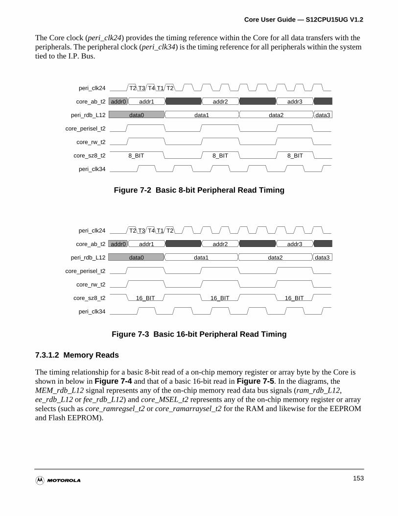
Core User Guide — S12CPU15UG V1.2
them
re is
ay
The Core clock (peri_clk24) provides the timing reference within the Core for all data transfers with peripherals. The peripheral clock (peri_clk34) is the timing reference for all peripherals within the systetied to the I.P. Bus.
Figure 7-2 Basic 8-bit Peripheral Read Timing
Figure 7-3 Basic 16-bit Peripheral Read Timing
7.3.1.2 Memory Reads
The timing relationship for a basic 8-bit read of a on-chip memory register or array byte by the Coshown in below inFigure 7-4 and that of a basic 16-bit read inFigure 7-5 . In the diagrams, theMEM_rdb_L12 signal represents any of the on-chip memory read data bus signals (ram_rdb_L12,ee_rdb_L12 or fee_rdb_L12) andcore_MSEL_t2 represents any of the on-chip memory register or arrselects (such ascore_ramregsel_t2 or core_ramarraysel_t2 for the RAM and likewise for the EEPROMand Flash EEPROM).
T2 T3 T4 T1 T2
addr0 addr1 addr2 addr3
data0 data1 data2 data3
8_BIT 8_BIT 8_BIT
peri_clk24
core_ab_t2
peri_rdb_L12
core_perisel_t2
core_rw_t2
core_sz8_t2
peri_clk34
T2 T3 T4 T1 T2
addr0 addr1 addr2 addr3
data0 data1 data2 data3
16_BIT 16_BIT 16_BIT
peri_clk24
core_ab_t2
peri_rdb_L12
core_perisel_t2
core_rw_t2
core_sz8_t2
peri_clk34
153
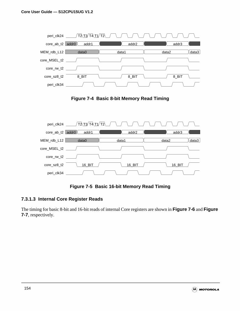
Core User Guide — S12CPU15UG V1.2
Figure 7-4 Basic 8-bit Memory Read Timing
Figure 7-5 Basic 16-bit Memory Read Timing
7.3.1.3 Internal Core Register Reads
The timing for basic 8-bit and 16-bit reads of internal Core registers are shown inFigure 7-6 andFigure7-7, respectively.
T2 T3 T4 T1 T2
addr0 addr1 addr2 addr3
data0 data1 data2 data3
8_BIT 8_BIT 8_BIT
peri_clk24
core_ab_t2
MEM_rdb_L12
core_MSEL_t2
core_rw_t2
core_sz8_t2
peri_clk34
T2 T3 T4 T1 T2
addr0 addr1 addr2 addr3
data0 data1 data2 data3
16_BIT 16_BIT 16_BIT
peri_clk24
core_ab_t2
MEM_rdb_L12
core_MSEL_t2
core_rw_t2
core_sz8_t2
peri_clk34
154
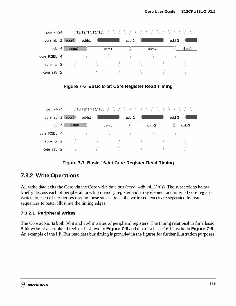
Core User Guide — S12CPU15UG V1.2
gisterd
basic
oses.
Figure 7-6 Basic 8-bit Core Register Read Timing
Figure 7-7 Basic 16-bit Core Register Read Timing
7.3.2 Write Operations
All write data exits the Core via the Core write data bus (core_wdb_t4[15:0]). The subsections belowbriefly discuss each of peripheral, on-chip memory register and array element and internal core rewrites. In each of the figures used in these subsections, the write sequences are separated by reasequences to better illustrate the timing edges.
7.3.2.1 Peripheral Writes
The Core supports both 8-bit and 16-bit writes of peripheral registers. The timing relationship for a8-bit write of a peripheral register is shown inFigure 7-8 and that of a basic 16-bit write inFigure 7-9 .An example of the I.P. Bus read data bus timing is provided in the figures for further illustration purp
T2 T3 T4 T1 T2
addr0 addr1 addr2 addr3
data0 data1 data2 data3
peri_clk24
core_ab_t2
rdb_t4
core_RSEL_t4
core_rw_t2
core_sz8_t2
T2 T3 T4 T1 T2
addr0 addr1 addr2 addr3
data0 data1 data2 data3
peri_clk24
core_ab_t2
rdb_t4
core_RSEL_t4
core_rw_t2
core_sz8_t2
155
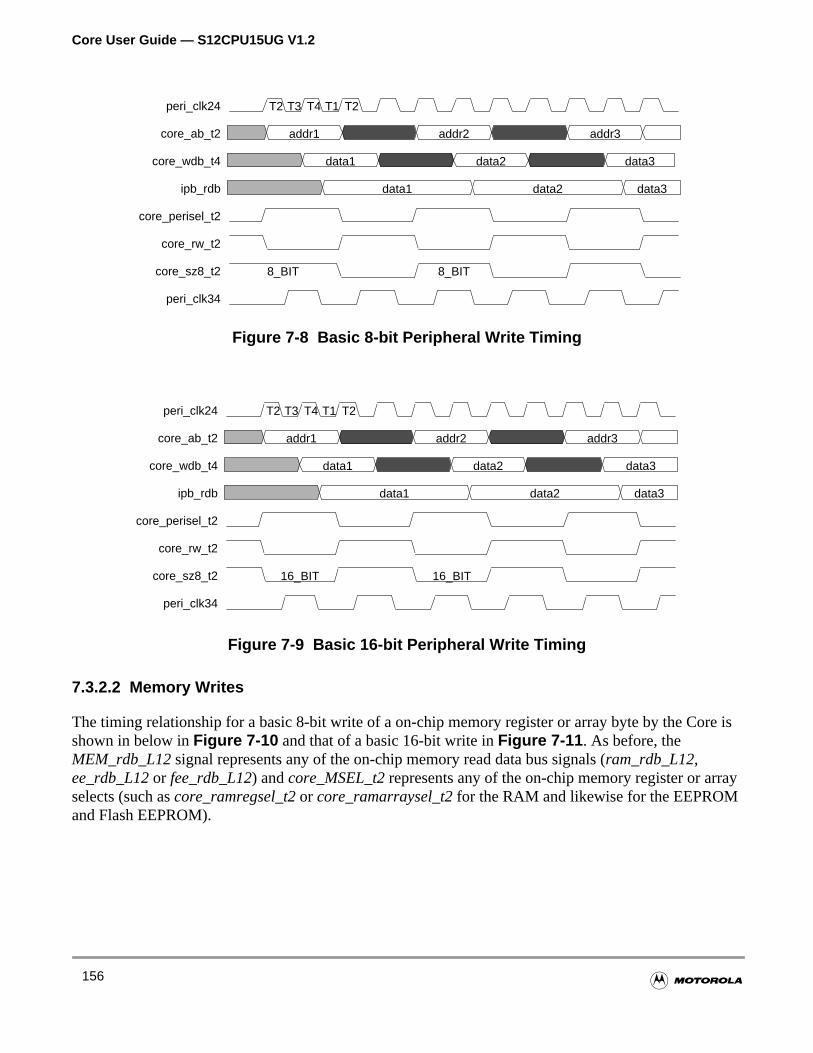
Core User Guide — S12CPU15UG V1.2
re is
ay
Figure 7-8 Basic 8-bit Peripheral Write Timing
Figure 7-9 Basic 16-bit Peripheral Write Timing
7.3.2.2 Memory Writes
The timing relationship for a basic 8-bit write of a on-chip memory register or array byte by the Coshown in below inFigure 7-10 and that of a basic 16-bit write inFigure 7-11 . As before, theMEM_rdb_L12 signal represents any of the on-chip memory read data bus signals (ram_rdb_L12,ee_rdb_L12 or fee_rdb_L12) andcore_MSEL_t2 represents any of the on-chip memory register or arrselects (such ascore_ramregsel_t2 or core_ramarraysel_t2 for the RAM and likewise for the EEPROMand Flash EEPROM).
T2 T3 T4 T1 T2
addr1 addr2 addr3
data1 data2 data3
data1 data2 data3
8_BIT 8_BIT
peri_clk24
core_ab_t2
core_wdb_t4
ipb_rdb
core_perisel_t2
core_rw_t2
core_sz8_t2
peri_clk34
T2 T3 T4 T1 T2
addr1 addr2 addr3
data1 data2 data3
data1 data2 data3
16_BIT 16_BIT
peri_clk24
core_ab_t2
core_wdb_t4
ipb_rdb
core_perisel_t2
core_rw_t2
core_sz8_t2
peri_clk34
156
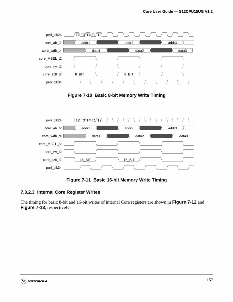
Core User Guide — S12CPU15UG V1.2
Figure 7-10 Basic 8-bit Memory Write Timing
Figure 7-11 Basic 16-bit Memory Write Timing
7.3.2.3 Internal Core Register Writes
The timing for basic 8-bit and 16-bit writes of internal Core registers are shown inFigure 7-12 andFigure 7-13 , respectively.
T2 T3 T4 T1 T2
addr1 addr2 addr3
data1 data2 data3
8_BIT 8_BIT
peri_clk24
core_ab_t2
core_wdb_t4
core_MSEL_t2
core_rw_t2
core_sz8_t2
peri_clk34
T2 T3 T4 T1 T2
addr1 addr2 addr3
data1 data2 data3
16_BIT 16_BIT
peri_clk24
core_ab_t2
core_wdb_t4
core_MSEL_t2
core_rw_t2
core_sz8_t2
peri_clk34
157
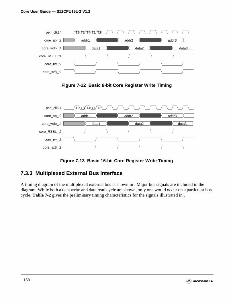
Core User Guide — S12CPU15UG V1.2
ear bus
Figure 7-12 Basic 8-bit Core Register Write Timing
Figure 7-13 Basic 16-bit Core Register Write Timing
7.3.3 Multiplexed External Bus Interface
A timing diagram of the multiplexed external bus is shown in . Major bus signals are included in thdiagram. While both a data write and data read cycle are shown, only one would occur on a particulcycle.Table 7-2 gives the preliminary timing characteristics for the signals illustrated in .
T2 T3 T4 T1 T2
addr1 addr2 addr3
data1 data2 data3
peri_clk24
core_ab_t2
core_wdb_t4
core_RSEL_t4
core_rw_t2
core_sz8_t2
T2 T3 T4 T1 T2
addr1 addr2 addr3
data1 data2 data3
peri_clk24
core_ab_t2
core_wdb_t4
core_RSEL_t2
core_rw_t2
core_sz8_t2
158
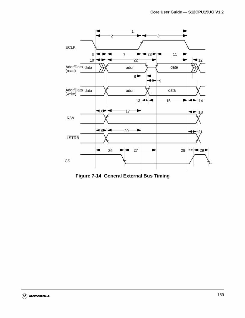
Core User Guide — S12CPU15UG V1.2
Figure 7-14 General External Bus Timing
Addr/Data(read)
Addr/Data(write)
addr datadata
5 11
12
9
237
ECLK
12 3
R/W
LSTRB
16 17 18
19 20 21
addr datadata
13
2210
8
15 14
CS
2726 28 29
159
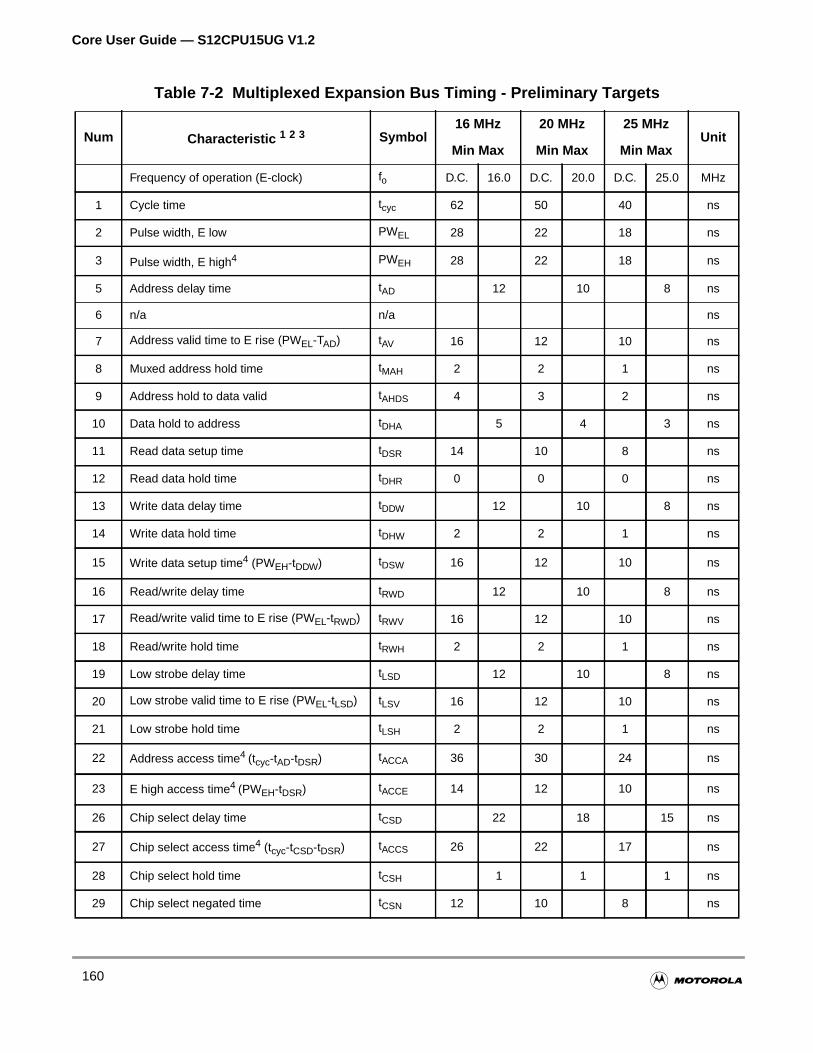
Core User Guide — S12CPU15UG V1.2
Table 7-2 Multiplexed Expansion Bus Timing - Preliminary Targets
Num Characteristic 1 2 3 Symbol16 MHz
Min Max
20 MHz
Min Max
25 MHz
Min MaxUnit
Frequency of operation (E-clock) fo D.C. 16.0 D.C. 20.0 D.C. 25.0 MHz
1 Cycle time tcyc 62 50 40 ns
2 Pulse width, E low PWEL 28 22 18 ns
3 Pulse width, E high4 PWEH 28 22 18 ns
5 Address delay time tAD 12 10 8 ns
6 n/a n/a ns
7 Address valid time to E rise (PWEL-TAD) tAV 16 12 10 ns
8 Muxed address hold time tMAH 2 2 1 ns
9 Address hold to data valid tAHDS 4 3 2 ns
10 Data hold to address tDHA 5 4 3 ns
11 Read data setup time tDSR 14 10 8 ns
12 Read data hold time tDHR 0 0 0 ns
13 Write data delay time tDDW 12 10 8 ns
14 Write data hold time tDHW 2 2 1 ns
15 Write data setup time4 (PWEH-tDDW) tDSW 16 12 10 ns
16 Read/write delay time tRWD 12 10 8 ns
17 Read/write valid time to E rise (PWEL-tRWD) tRWV 16 12 10 ns
18 Read/write hold time tRWH 2 2 1 ns
19 Low strobe delay time tLSD 12 10 8 ns
20 Low strobe valid time to E rise (PWEL-tLSD) tLSV 16 12 10 ns
21 Low strobe hold time tLSH 2 2 1 ns
22 Address access time4 (tcyc-tAD-tDSR) tACCA 36 30 24 ns
23 E high access time4 (PWEH-tDSR) tACCE 14 12 10 ns
26 Chip select delay time tCSD 22 18 15 ns
27 Chip select access time4 (tcyc-tCSD-tDSR) tACCS 26 22 17 ns
28 Chip select hold time tCSH 1 1 1 ns
29 Chip select negated time tCSN 12 10 8 ns
160
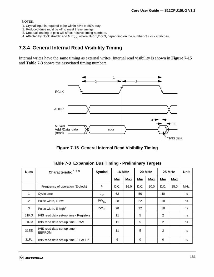
Core User Guide — S12CPU15UG V1.2
7.3.4 General Internal Read Visibility Timing
Internal writes have the same timing as external writes. Internal read visibility is shown inFigure 7-15andTable 7-3 shows the associated timing numbers.
Figure 7-15 General Internal Read Visibility Timing
NOTES:1. Crystal input is required to be within 45% to 55% duty.2. Reduced drive must be off to meet these timings.3. Unequal loading of pins will affect relative timing numbers.4. Affected by clock stretch: add N x tcyc where N=0,1,2 or 3, depending on the number of clock stretches.
Table 7-3 Expansion Bus Timing - Preliminary Targets
Num Characteristic 1 2 3 Symbol 16 MHz 20 MHz 25 MHz Unit
Min Max Min Max Min Max
Frequency of operation (E-clock) fo D.C. 16.0 D.C. 20.0 D.C. 25.0 MHz
1 Cycle time tcyc 62 50 40 ns
2 Pulse width, E low PWEL 28 22 18 ns
3 Pulse width, E high4 PWEH 28 22 18 ns
31RG IVIS read data set-up time - Registers 11 5 2 ns
31RM IVIS read data set-up time - RAM 11 5 2 ns
31EEIVIS read data set-up time -EEPROM
11 5 2 ns
31FL IVIS read data set-up time - FLASH5 6 0 0 ns
ECLK
ADDR
12 3
3132
IVIS data
Muxedaddrdata
(read)Addr/Data
161
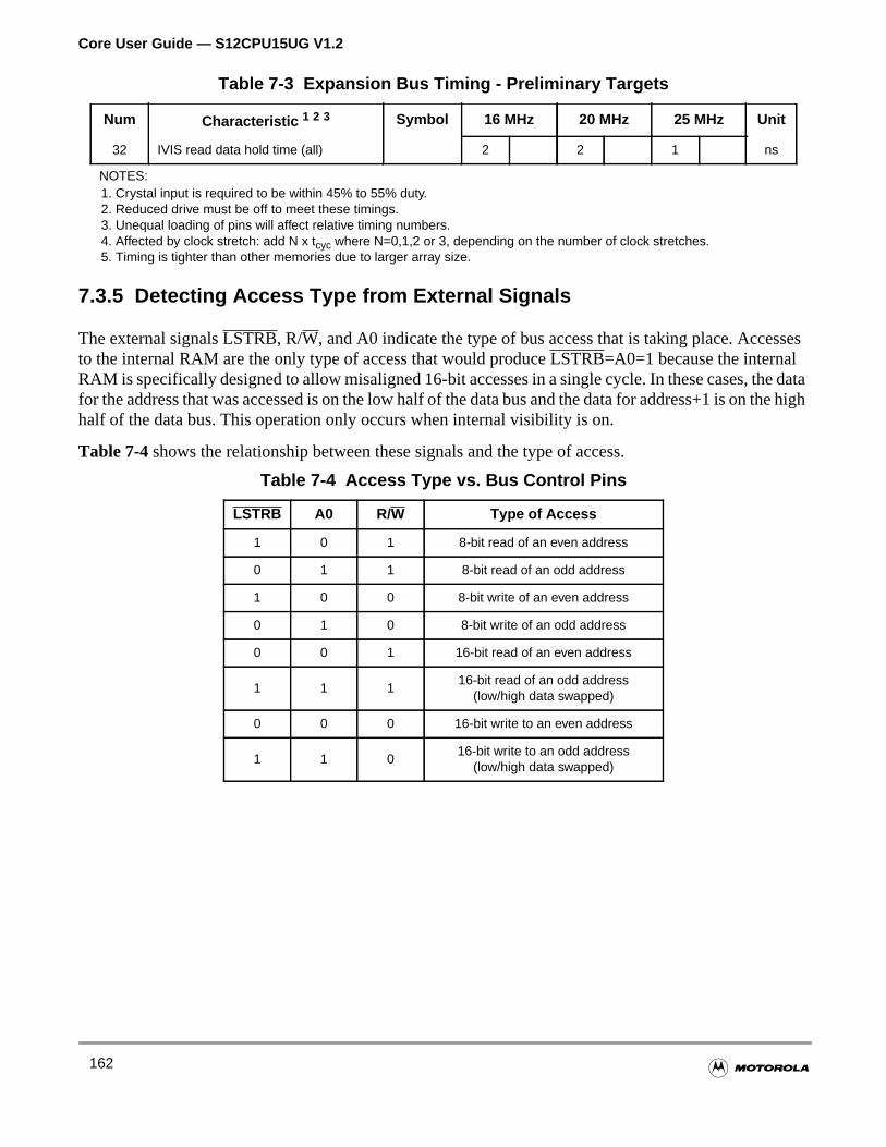
Core User Guide — S12CPU15UG V1.2
sses
e datathe high
7.3.5 Detecting Access Type from External Signals
The external signalsLSTRB, R/W, and A0 indicate the type of bus access that is taking place. Acceto the internal RAM are the only type of access that would produceLSTRB=A0=1 because the internalRAM is specifically designed to allow misaligned 16-bit accesses in a single cycle. In these cases, thfor the address that was accessed is on the low half of the data bus and the data for address+1 is onhalf of the data bus. This operation only occurs when internal visibility is on.
Table 7-4 shows the relationship between these signals and the type of access.
32 IVIS read data hold time (all) 2 2 1 ns
NOTES:1. Crystal input is required to be within 45% to 55% duty.2. Reduced drive must be off to meet these timings.3. Unequal loading of pins will affect relative timing numbers.4. Affected by clock stretch: add N x tcyc where N=0,1,2 or 3, depending on the number of clock stretches.5. Timing is tighter than other memories due to larger array size.
Table 7-4 Access Type vs. Bus Control Pins
LSTRB A0 R/ W Type of Access
1 0 1 8-bit read of an even address
0 1 1 8-bit read of an odd address
1 0 0 8-bit write of an even address
0 1 0 8-bit write of an odd address
0 0 1 16-bit read of an even address
1 1 116-bit read of an odd address
(low/high data swapped)
0 0 0 16-bit write to an even address
1 1 016-bit write to an odd address
(low/high data swapped)
Table 7-3 Expansion Bus Timing - Preliminary Targets
Num Characteristic 1 2 3 Symbol 16 MHz 20 MHz 25 MHz Unit
162
Core User Guide — S12CPU15UG V1.2
cuss
testduct(s) toclock
ariousal Timeals is
Section 8 Core Clock and Reset Connections
This section details the HCS12 V1.5 Core external clock connections. In addition, this section will disthe reset timing needs of the Core since this is associated very closely with the external clockingrequirements.
8.1 Clocking Overview
The HCS12 V1.5 Core is implemented as a single clock source design with complete Mux-D scanimplementation. Since the Core is compatible with the feature set of the MHC12 microcontroller profamily, many signal and timing requirements exist for the system clock and reset generation blocksupport these features. Many of these requirements are driven by the interaction of the Core with theand reset generation block(s) in the system due to CPU wait and stop mode functionality and the vtime based reset and interrupt functions (such as Crystal Monitor and COP Watchdog resets and ReInterrupt functions) available on the HCS12 family of products. A diagram of the Core interface signgiven inFigure 8-1 below.
163
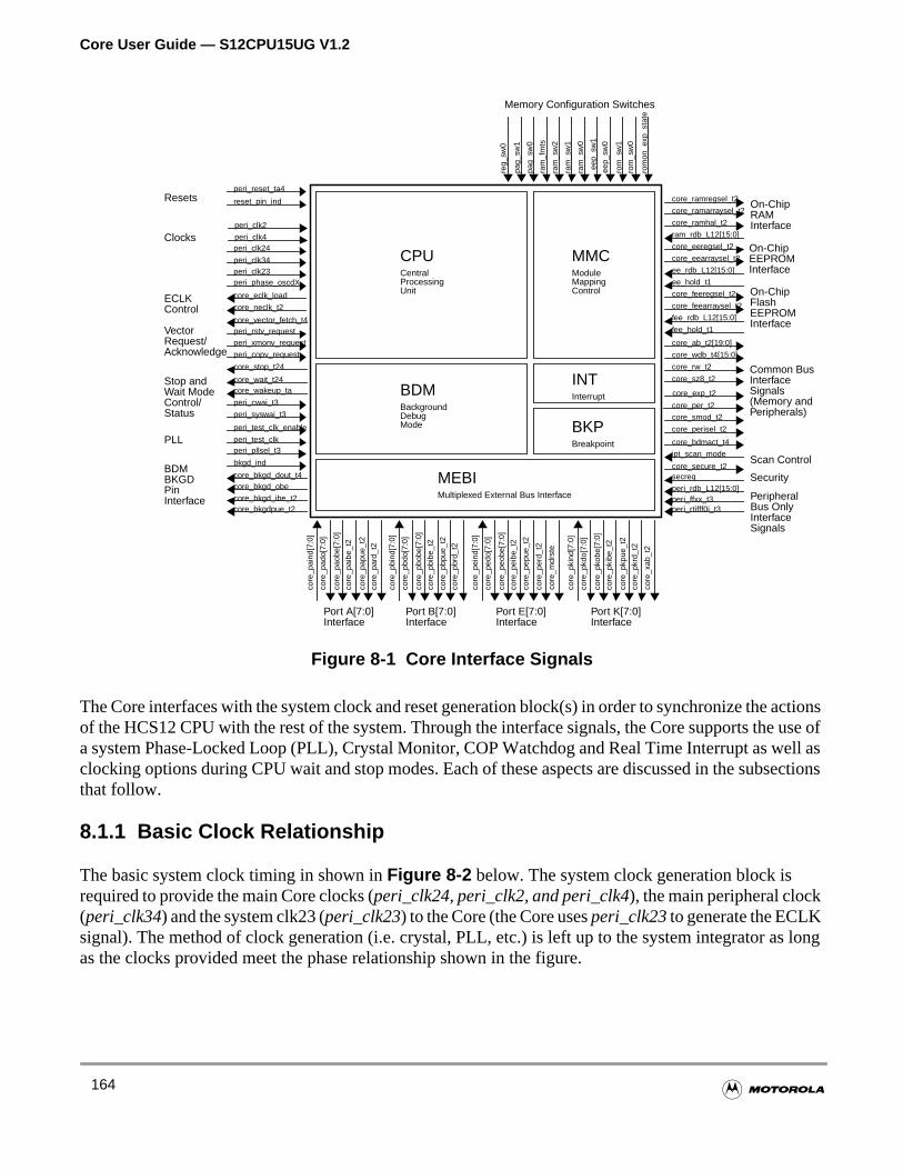
Core User Guide — S12CPU15UG V1.2
ctionsuse ofell asections
long
Figure 8-1 Core Interface Signals
The Core interfaces with the system clock and reset generation block(s) in order to synchronize the aof the HCS12 CPU with the rest of the system. Through the interface signals, the Core supports thea system Phase-Locked Loop (PLL), Crystal Monitor, COP Watchdog and Real Time Interrupt as wclocking options during CPU wait and stop modes. Each of these aspects are discussed in the substhat follow.
8.1.1 Basic Clock Relationship
The basic system clock timing in shown inFigure 8-2 below. The system clock generation block isrequired to provide the main Core clocks (peri_clk24, peri_clk2, and peri_clk4), the main peripheral clock(peri_clk34) and the system clk23 (peri_clk23) to the Core (the Core usesperi_clk23to generate the ECLKsignal). The method of clock generation (i.e. crystal, PLL, etc.) is left up to the system integrator asas the clocks provided meet the phase relationship shown in the figure.
reset_pin_ind
peri_clk24
peri_clk23peri_clk34
peri_rdb_L12[15:0]peri_ffxx_t3peri_rtifff0i_t3
core_ramarraysel_t2
core_ab_t2[19:0]
core_wdb_t4[15:0]
core_rw_t2
core_sz8_t2
core_smod_t2
core_perisel_t2
core_bdmact_t4
ram_rdb_L12[15:0]
core_ramregsel_t2
core_eeregsel_t2
core_eearraysel_t2
ee_rdb_L12[15:0]
ee_hold_t1
core_feeregsel_t2
core_feearraysel_t2
fee_rdb_L12[15:0]
fee_hold_t1
core_secure_t2secreq
peri_reset_ta4
core_stop_t24
peri_phase_oscdX
peri_xmonv_request
peri_rstv_request
peri_copv_request
core_wakeup_tacore_wait_t24
peri_cwai_t3
peri_syswai_t3
peri_test_clk_enable
peri_pllsel_t3peri_test_clk
bkgd_ind
core_bkgd_obecore_bkgd_dout_t4
core_bkgd_ibe_t2core_bkgdpue_t2
core
_pai
nd[7
:0]
core
_pad
o[7:
0]
core
_pao
be[7
:0]
core
_pai
be_t
2
core
_pap
ue_t
2
core
_par
d_t2
core
_pei
nd[7
:0]
core
_ped
o[7:
0]
core
_peo
be[7
:0]
core
_pei
be_t
2
core
_pep
ue_t
2
core
_per
d_t2
core
_mdr
ste
core
_pbi
nd[7
:0]
core
_pbd
o[7:
0]
core
_pbo
be[7
:0]
core
_pbi
be_t
2
core
_pbp
ue_t
2
core
_pbr
d_t2
core
_pki
nd[7
:0]
core
_pkd
o[7:
0]
core
_pko
be[7
:0]
core
_pki
be_t
2
core
_pkp
ue_t
2
core
_pkr
d_t2
core
_xab
_t2
reg_
sw0
pag_
sw0
ram
_sw
2
ram
_sw
1
ram
_sw
0
eep_
sw1
eep_
sw0
rom
_sw
1
rom
_sw
0
rom
on_e
xp_s
tate
pag_
sw1
BDMBackgroundDebugMode
CPUCentralProcessingUnit
MMCModuleMappingControl
INTInterrupt
BKPBreakpoint
MEBIMultiplexed External Bus Interface
Port A[7:0]Interface
Port B[7:0]Interface
Port E[7:0]Interface
Port K[7:0]Interface
PeripheralBus OnlyInterfaceSignals
Security
Common BusInterfaceSignals(Memory andPeripherals)
On-Chip
On-ChipEEPROMInterface
On-ChipRAMInterface
Memory Configuration Switches
Resets
Clocks
VectorRequest/Acknowledge
Stop andWait ModeControl/Status
PLL
BDMBKGDPinInterface
FlashEEPROMInterface
core_eclk_load
core_neclk_t2
core_vector_fetch_t4
ECLKControl
core_ramhal_t2
ipt_scan_modeScan Control
core_exp_t2
ram
_fm
ts
peri_clk4
peri_clk2
core_per_t2
164
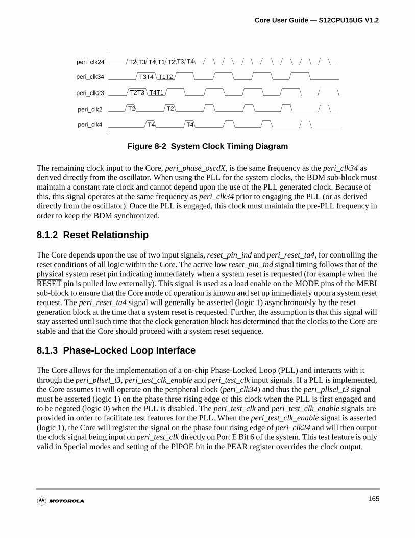
Core User Guide — S12CPU15UG V1.2
ustuse of
cy in
en theEBI
m reset
nal willore are
it
ed and
lyt.
Figure 8-2 System Clock Timing Diagram
The remaining clock input to the Core,peri_phase_oscdX, is the same frequency as theperi_clk34 asderived directly from the oscillator. When using the PLL for the system clocks, the BDM sub-block mmaintain a constant rate clock and cannot depend upon the use of the PLL generated clock. Becathis, this signal operates at the same frequency asperi_clk34 prior to engaging the PLL (or as deriveddirectly from the oscillator). Once the PLL is engaged, this clock must maintain the pre-PLL frequenorder to keep the BDM synchronized.
8.1.2 Reset Relationship
The Core depends upon the use of two input signals,reset_pin_indandperi_reset_ta4, for controlling thereset conditions of all logic within the Core. The active lowreset_pin_indsignal timing follows that of thephysical system reset pin indicating immediately when a system reset is requested (for example whRESET pin is pulled low externally). This signal is used as a load enable on the MODE pins of the Msub-block to ensure that the Core mode of operation is known and set up immediately upon a systerequest. Theperi_reset_ta4 signal will generally be asserted (logic 1) asynchronously by the resetgeneration block at the time that a system reset is requested. Further, the assumption is that this sigstay asserted until such time that the clock generation block has determined that the clocks to the Cstable and that the Core should proceed with a system reset sequence.
8.1.3 Phase-Locked Loop Interface
The Core allows for the implementation of a on-chip Phase-Locked Loop (PLL) and interacts withthrough theperi_pllsel_t3, peri_test_clk_enableandperi_test_clkinput signals. If a PLL is implemented,the Core assumes it will operate on the peripheral clock (peri_clk34) and thus theperi_pllsel_t3 signalmust be asserted (logic 1) on the phase three rising edge of this clock when the PLL is first engagto be negated (logic 0) when the PLL is disabled. Theperi_test_clk andperi_test_clk_enable signals areprovided in order to facilitate test features for the PLL. When theperi_test_clk_enable signal is asserted(logic 1), the Core will register the signal on the phase four rising edge ofperi_clk24and will then outputthe clock signal being input onperi_test_clkdirectly on Port E Bit 6 of the system. This test feature is onvalid in Special modes and setting of the PIPOE bit in the PEAR register overrides the clock outpu
T2 T3 T4 T1 T2
T3T4 T1T2
peri_clk24
peri_clk34
T2T3 T4T1peri_clk23
T3 T4
peri_clk4
T2 T2
T4 T4
peri_clk2
165
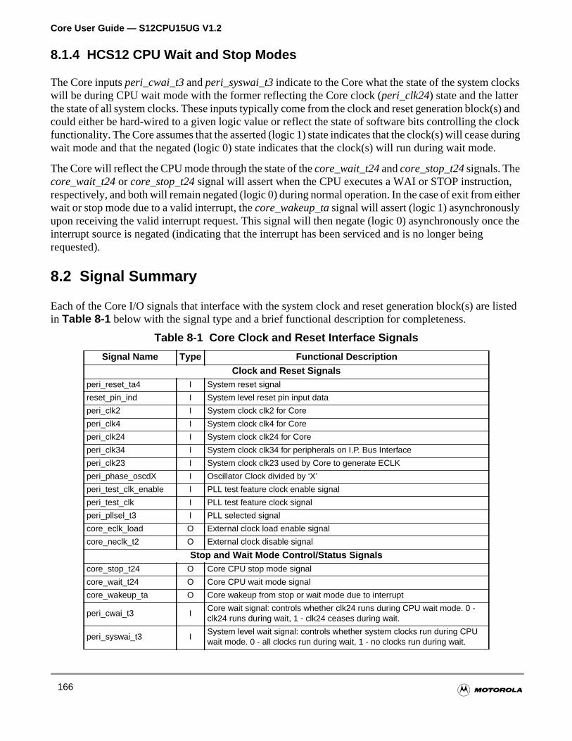
Core User Guide — S12CPU15UG V1.2
ks
s) andlockduring.
n,ither
e the
listed
8.1.4 HCS12 CPU Wait and Stop Modes
The Core inputsperi_cwai_t3andperi_syswai_t3indicate to the Core what the state of the system clocwill be during CPU wait mode with the former reflecting the Core clock (peri_clk24) state and the latterthe state of all system clocks. These inputs typically come from the clock and reset generation block(could either be hard-wired to a given logic value or reflect the state of software bits controlling the cfunctionality. The Core assumes that the asserted (logic 1) state indicates that the clock(s) will ceasewait mode and that the negated (logic 0) state indicates that the clock(s) will run during wait mode
The Core will reflect the CPU mode through the state of thecore_wait_t24andcore_stop_t24signals. Thecore_wait_t24 or core_stop_t24 signal will assert when the CPU executes a WAI or STOP instructiorespectively, and both will remain negated (logic 0) during normal operation. In the case of exit from ewait or stop mode due to a valid interrupt, thecore_wakeup_tasignal will assert (logic 1) asynchronouslyupon receiving the valid interrupt request. This signal will then negate (logic 0) asynchronously oncinterrupt source is negated (indicating that the interrupt has been serviced and is no longer beingrequested).
8.2 Signal Summary
Each of the Core I/O signals that interface with the system clock and reset generation block(s) arein Table 8-1 below with the signal type and a brief functional description for completeness.
Table 8-1 Core Clock and Reset Interface Signals
Signal Name Type Functional Description
Clock and Reset Signalsperi_reset_ta4 I System reset signal
reset_pin_ind I System level reset pin input data
peri_clk2 I System clock clk2 for Core
peri_clk4 I System clock clk4 for Core
peri_clk24 I System clock clk24 for Core
peri_clk34 I System clock clk34 for peripherals on I.P. Bus Interface
peri_clk23 I System clock clk23 used by Core to generate ECLK
peri_phase_oscdX I Oscillator Clock divided by ‘X’
peri_test_clk_enable I PLL test feature clock enable signal
peri_test_clk I PLL test feature clock signal
peri_pllsel_t3 I PLL selected signal
core_eclk_load O External clock load enable signal
core_neclk_t2 O External clock disable signal
Stop and Wait Mode Control/Status Signalscore_stop_t24 O Core CPU stop mode signal
core_wait_t24 O Core CPU wait mode signal
core_wakeup_ta O Core wakeup from stop or wait mode due to interrupt
peri_cwai_t3 ICore wait signal: controls whether clk24 runs during CPU wait mode. 0 -clk24 runs during wait, 1 - clk24 ceases during wait.
peri_syswai_t3 ISystem level wait signal: controls whether system clocks run during CPUwait mode. 0 - all clocks run during wait, 1 - no clocks run during wait.
166
Core User Guide — S12CPU15UG V1.2
. Alsosetlt the
Port
essed
keep
8.3 Detailed Clock and Reset Signal Descriptions
General descriptions of the Core clock and reset interface signals are given in the subsections belowincluded are the stop and wait mode signals due to the necessary interaction with the clock and rerequirements. For detailed descriptions of these signals including timing information please consuHCS12 V1.5 Core Integration Guide.
8.3.1 Clock and Reset Signals
These descriptions apply to system level clock and reset signals needed by the Core.
8.3.1.1 System Reset signal (peri_reset_ta4)
This single bit asynchronous input to the Core indicates the system reset condition.
8.3.1.2 System level reset input data (reset_pin_ind)
This active-low single bit input is used within the Core as a load enable for the MODE pin logic onE of the system.
8.3.1.3 System level clock for the Core (peri_clk2)
This clock input is one of the main clocks for the Core.
8.3.1.4 System level clock for the Core (peri_clk4)
This clock input is one of the main clocks for the Core.
8.3.1.5 System level clock for the Core (peri_clk24)
This clock input is one of the main clocks for the Core.
8.3.1.6 System level clock for peripheral blocks (peri_clk34)
This clock input is the main clock source for all peripheral blocks integrated in the system and accby the Core through the I.P. Bus Interface.
8.3.1.7 System ECLK clock (peri_clk23)
This clock input is the main clock source used by the Core to generate the system ECLK.
8.3.1.8 Divided Down System Oscillator Clock (peri_phase_oscdX)
This clock input to the Core is used within the Core by the Background Debug Mode sub-block tothe BDM synchronized.
167
Core User Guide — S12CPU15UG V1.2
ut on
tal or
s
is ready
de.
8.3.1.9 System Test Clock enable (peri_test_clk_enable)
This single bit input to the Core indicates that the phase-locked loop (PLL) test clock should be outpthe system Port E bit 6 pin when the PIPOE bit is zero.
8.3.1.10 System Test Clock (peri_test_clk)
This clock input to the Core is the PLL test clock.
8.3.1.11 System clock source select signal (peri_pllsel_t3)
This single bit input to the Core indicates whether clocks within the system are derived from the crysPLL.
8.3.1.12 ECLK load enable signal (core_eclk_load)
This single bit output from the Core is the load enable signal for the system external clock, ECLK.
8.3.1.13 ECLK disable signal (core_neclk_t2)
This single bit output from the Core is the disable signal for the system external clock, ECLK.
8.3.2 Stop and Wait Mode Control/Status Signals
These descriptions apply to signals that provide for controlling some of the functionality and statuindication of CPU stop and wait modes.
8.3.2.1 CPU stop mode indicator (core_stop_t24)
This Core output signal indicates whether the CPU is in stop mode.
8.3.2.2 CPU wait mode indicator (core_wait_t24)
This Core output signal indicates whether the CPU is in wait mode.
8.3.2.3 Core wakeup indicator for wait and stop mode (core_wakeup_ta)
This asynchronous Core output signal indicates that the CPU has received an interrupt request andto resume normal operation.
8.3.2.4 Core wait signal from system clock generation block (peri_cwai_t3)
This Core input signal indicates to the CPU whether the main Core clock,peri_clk24, will run during CPUwait mode.
8.3.2.5 System level wait signal (peri_syswai_t3)
This Core input signal indicates to the Core whether all system clocks will run during CPU wait mo
168
Core User Guide — S12CPU15UG V1.2
S)Core
Section 9 Core Power Connections
This section details the HCS12 V1.5 Core power connections.
9.1 Power Overview
The HCS12 V1.5 Core operates from a single power and a single ground connection.
9.1.1 Power and Ground Summary
The Core requires a single power (typically termed VDD) and a single ground (typically termed VSconnection that is implicit when integrating into a synthesized design. There are no signals at the interface for power and ground.
169

Core User Guide — S12CPU15UG V1.2
170
Core User Guide — S12CPU15UG V1.2
licablets, andests are
or
e
he
Section 10 Interrupt (INT)
This section describes the functionality of the Interrupt (INT) sub-block of the Core.
10.1 Overview
The Interrupt sub-block decodes the priority of all system exception requests and provides the appvector for processing the exception. The INT supports I-bit maskable and X-bit maskable interrupnonmaskable Unimplemented Opcode Trap, a nonmaskable software interrupt (SWI) or BackgrouDebug Mode request, and three system reset vector requests. All interrupt related exception requhandled by the Interrupt.
10.1.1 Features
• Provides 2 to 122 I bit maskable interrupt vectors ($FF00-$FFF2)
• Provides 1 X bit maskable interrupt vector ($FFF4)
• Provides a nonmaskable Unimplemented Opcode Trap (TRAP) vector ($FFF8)
• Provides a nonmaskable software interrupt (SWI) or Background Debug Mode request vect($FFF6)
• Provides 3 system reset vectors ($FFFA-$FFFE)
• Determines the appropriate vector and drives it onto the address bus at the appropriate tim
• Signals the CPU that interrupts are pending
• Provides control registers which allow testing of interrupts
• Provides additional input signals which prevents requests for servicing I and X interrupts
• Wakes the system from stop or wait mode when an appropriate interrupt occurs or wheneverXIRQis active, even ifXIRQ is masked
• Provides asynchronous path for all I and X interrupts, ($FF00–$FFF4)
• (Optional) Selects and stores the highest priority I interrupt based on the value written into tHPRIO register
171
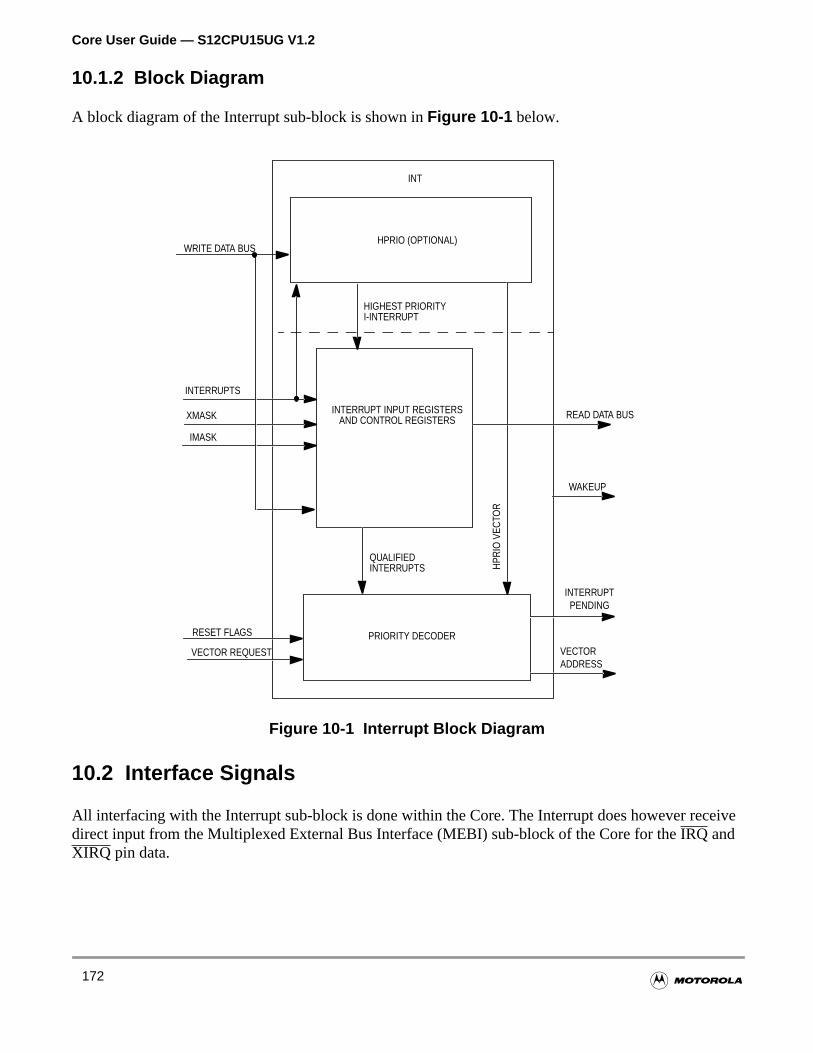
Core User Guide — S12CPU15UG V1.2
eive
10.1.2 Block Diagram
A block diagram of the Interrupt sub-block is shown inFigure 10-1 below.
Figure 10-1 Interrupt Block Diagram
10.2 Interface Signals
All interfacing with the Interrupt sub-block is done within the Core. The Interrupt does however recdirect input from the Multiplexed External Bus Interface (MEBI) sub-block of the Core for theIRQ andXIRQ pin data.
HPRIO (OPTIONAL)
INT
PRIORITY DECODER
VECTOR REQUESTADDRESS
INTERRUPT
INTERRUPTS
RESET FLAGS
WRITE DATA BUS
HPR
IO V
ECTO
R
XMASK
IMASK
QUALIFIED
INTERRUPT INPUT REGISTERS
INTERRUPTS
AND CONTROL REGISTERS
HIGHEST PRIORITYI-INTERRUPT
PENDING
VECTOR
READ DATA BUS
WAKEUP
172
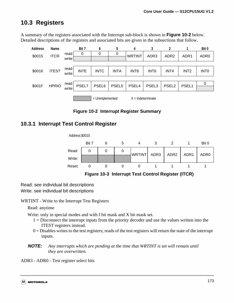
Core User Guide — S12CPU15UG V1.2
the
errupt
10.3 Registers
A summary of the registers associated with the Interrupt sub-block is shown inFigure 10-2 below.Detailed descriptions of the registers and associated bits are given in the subsections that follow.
Figure 10-2 Interrupt Register Summary
10.3.1 Interrupt Test Control Register
Read: see individual bit descriptionsWrite: see individual bit descriptions
WRTINT - Write to the Interrupt Test Registers
Read: anytime
Write: only in special modes and with I bit mask and X bit mask set.1 = Disconnect the interrupt inputs from the priority decoder and use the values written into
ITEST registers instead.0 = Disables writes to the test registers; reads of the test registers will return the state of the int
inputs.
NOTE: Any interrupts which are pending at the time that WRTINT is set will remain untilthey are overwritten.
ADR3 - ADR0 - Test register select bits
Address Name Bit 7 6 5 4 3 2 1 Bit 0
$0015 ITCRread 0 0 0
WRTINT ADR3 ADR2 ADR1 ADR0write
$0016 ITESTread
INTE INTC INTA INT8 INT6 INT4 INT2 INT0write
$001F HPRIOread
PSEL7 PSEL6 PSEL5 PSEL4 PSEL3 PSEL2 PSEL10
write
= Unimplemented X = Indeterminate
Address:$0015
Bit 7 6 5 4 3 2 1 Bit 0
Read: 0 0 0WRTINT ADR3 ADR2 ADR1 ADR0
Write:
Reset: 0 0 0 0 1 1 1 1
Figure 10-3 Interrupt Test Control Register (ITCR)
173
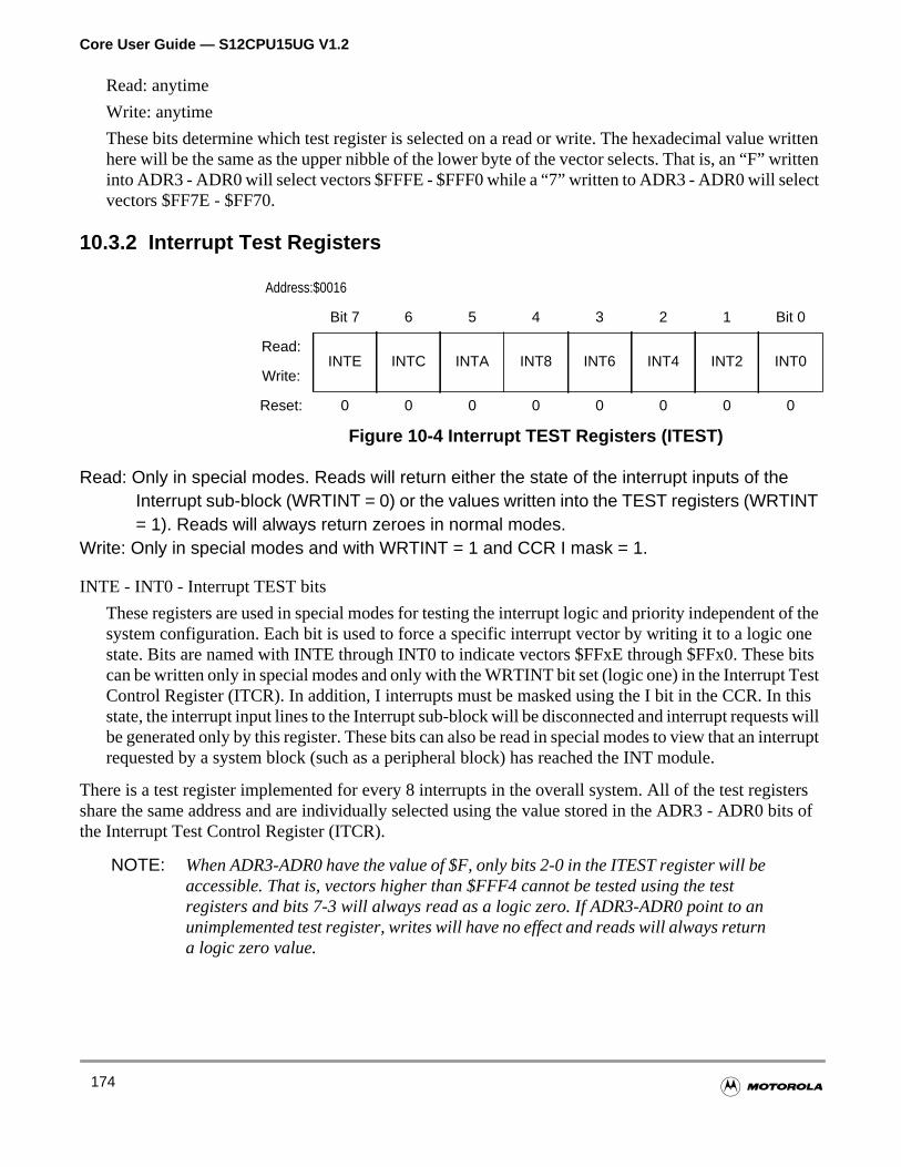
Core User Guide — S12CPU15UG V1.2
rittenrittent
of the onee bitsest
thists willterrupt
isters bits of
Read: anytime
Write: anytime
These bits determine which test register is selected on a read or write. The hexadecimal value where will be the same as the upper nibble of the lower byte of the vector selects. That is, an “F” winto ADR3 - ADR0 will select vectors $FFFE - $FFF0 while a “7” written to ADR3 - ADR0 will selecvectors $FF7E - $FF70.
10.3.2 Interrupt Test Registers
Read: Only in special modes. Reads will return either the state of the interrupt inputs of theInterrupt sub-block (WRTINT = 0) or the values written into the TEST registers (WRTINT= 1). Reads will always return zeroes in normal modes.
Write: Only in special modes and with WRTINT = 1 and CCR I mask = 1.
INTE - INT0 - Interrupt TEST bits
These registers are used in special modes for testing the interrupt logic and priority independentsystem configuration. Each bit is used to force a specific interrupt vector by writing it to a logicstate. Bits are named with INTE through INT0 to indicate vectors $FFxE through $FFx0. Thescan be written only in special modes and only with the WRTINT bit set (logic one) in the Interrupt TControl Register (ITCR). In addition, I interrupts must be masked using the I bit in the CCR. Instate, the interrupt input lines to the Interrupt sub-block will be disconnected and interrupt requesbe generated only by this register. These bits can also be read in special modes to view that an inrequested by a system block (such as a peripheral block) has reached the INT module.
There is a test register implemented for every 8 interrupts in the overall system. All of the test regshare the same address and are individually selected using the value stored in the ADR3 - ADR0the Interrupt Test Control Register (ITCR).
NOTE: When ADR3-ADR0 have the value of $F, only bits 2-0 in the ITEST register will beaccessible. That is, vectors higher than $FFF4 cannot be tested using the testregisters and bits 7-3 will always read as a logic zero. If ADR3-ADR0 point to anunimplemented test register, writes will have no effect and reads will always returna logic zero value.
Address:$0016
Bit 7 6 5 4 3 2 1 Bit 0
Read:INTE INTC INTA INT8 INT6 INT4 INT2 INT0
Write:
Reset: 0 0 0 0 0 0 0 0
Figure 10-4 Interrupt TEST Registers (ITEST)
174
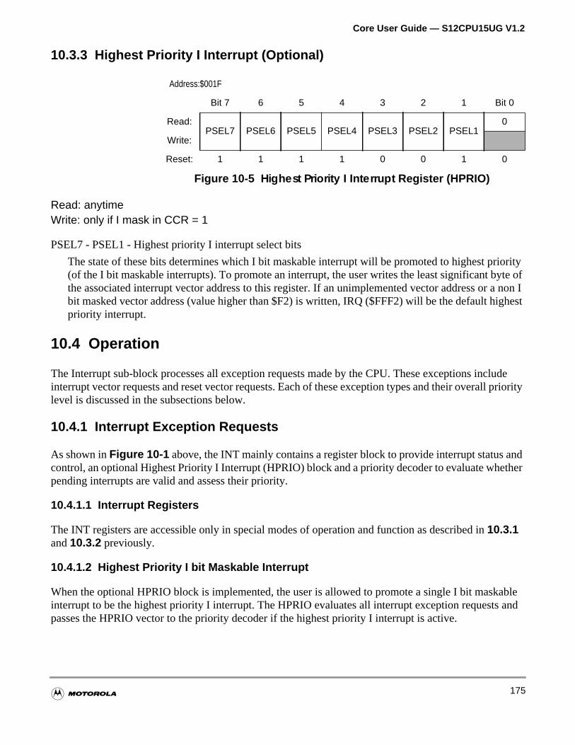
Core User Guide — S12CPU15UG V1.2
riorityte of a non Ihest
ludepriority
andther
kables and
10.3.3 Highest Priority I Interrupt (Optional)
Read: anytimeWrite: only if I mask in CCR = 1
PSEL7 - PSEL1 - Highest priority I interrupt select bits
The state of these bits determines which I bit maskable interrupt will be promoted to highest p(of the I bit maskable interrupts). To promote an interrupt, the user writes the least significant bythe associated interrupt vector address to this register. If an unimplemented vector address orbit masked vector address (value higher than $F2) is written, IRQ ($FFF2) will be the default higpriority interrupt.
10.4 Operation
The Interrupt sub-block processes all exception requests made by the CPU. These exceptions incinterrupt vector requests and reset vector requests. Each of these exception types and their overalllevel is discussed in the subsections below.
10.4.1 Interrupt Exception Requests
As shown inFigure 10-1 above, the INT mainly contains a register block to provide interrupt statuscontrol, an optional Highest Priority I Interrupt (HPRIO) block and a priority decoder to evaluate whepending interrupts are valid and assess their priority.
10.4.1.1 Interrupt Registers
The INT registers are accessible only in special modes of operation and function as described in10.3.1and10.3.2 previously.
10.4.1.2 Highest Priority I bit Maskable Interrupt
When the optional HPRIO block is implemented, the user is allowed to promote a single I bit masinterrupt to be the highest priority I interrupt. The HPRIO evaluates all interrupt exception requestpasses the HPRIO vector to the priority decoder if the highest priority I interrupt is active.
Address:$001F
Bit 7 6 5 4 3 2 1 Bit 0
Read:PSEL7 PSEL6 PSEL5 PSEL4 PSEL3 PSEL2 PSEL1
0
Write:
Reset: 1 1 1 1 0 0 1 0
Figure 10-5 Highest Priority I Interrupt Register (HPRIO)
175
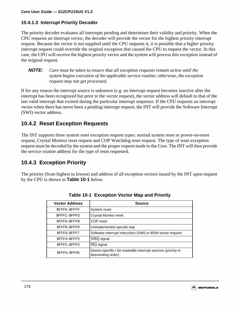
Core User Guide — S12CPU15UG V1.2
n thept
riorityIn thisad of
theof theerrupterrupt
esettionprovide
quest
10.4.1.3 Interrupt Priority Decoder
The priority decoder evaluates all interrupts pending and determines their validity and priority. WheCPU requests an interrupt vector, the decoder will provide the vector for the highest priority interrurequest. Because the vector is not supplied until the CPU requests it, it is possible that a higher pinterrupt request could override the original exception that caused the CPU to request the vector. case, the CPU will receive the highest priority vector and the system will process this exception instethe original request.
NOTE: Care must be taken to ensure that all exception requests remain active until thesystem begins execution of the applicable service routine; otherwise, the exceptionrequest may not get processed.
If for any reason the interrupt source is unknown (e.g. an interrupt request becomes inactive afterinterrupt has been recognized but prior to the vector request), the vector address will default to thatlast valid interrupt that existed during the particular interrupt sequence. If the CPU requests an intvector when there has never been a pending interrupt request, the INT will provide the Software Int(SWI) vector address.
10.4.2 Reset Exception Requests
The INT supports three system reset exception request types: normal system reset or power-on-rrequest, Crystal Monitor reset request and COP Watchdog reset request. The type of reset exceprequest must be decoded by the system and the proper request made to the Core. The INT will thenthe service routine address for the type of reset requested.
10.4.3 Exception Priority
The priority (from highest to lowest) and address of all exception vectors issued by the INT upon reby the CPU is shown inTable 10-1 below.
Table 10-1 Exception Vector Map and Priority
Vector Address Source
$FFFE–$FFFF System reset
$FFFC–$FFFD Crystal Monitor reset
$FFFA–$FFFB COP reset
$FFF8–$FFF9 Unimplemented opcode trap
$FFF6–$FFF7 Software interrupt instruction (SWI) or BDM vector request
$FFF4–$FFF5 XIRQ signal
$FFF2–$FFF3 IRQ signal
$FFF0–$FF00Device-specific I bit maskable interrupt sources (priority indescending order)
176
Core User Guide — S12CPU15UG V1.2
s that
ed in
ion of
ill be
ill be
10.5 Modes of Operation
The functionality of the INT sub-block in various modes of operation is discussed in the subsectionfollow.
10.5.1 Normal Operation
The INT operates the same in all normal modes of operation.
10.5.2 Special Operation
Interrupts may be tested in special modes through the use of the interrupt test registers as describ10.3.1 and10.3.2 previously.
10.5.3 Emulation Modes
The INT operates the same in emulation modes as in normal modes.
10.6 Low-Power Options
The INT does not contain any user-controlled options for reducing power consumption. The operatthe INT in low-power modes is discussed in the following subsections.
10.6.1 Run Mode
The INT does not contain any options for reducing power in run mode.
10.6.2 Wait Mode
Clocks to the INT can be shut off during system wait mode and the asynchronous interrupt path wused to generate the wakeup signal upon recognition of a valid interrupt or anyXIRQ request.
10.6.3 Stop Mode
Clocks to the INT can be shut off during system stop mode and the asynchronous interrupt path wused to generate the wakeup signal upon recognition of a valid interrupt or anyXIRQ request.
10.7 Motorola Internal Information
The INT does not contain any functionality that is considered to be for Motorola internal use only.
177

Core User Guide — S12CPU15UG V1.2
178
Core User Guide — S12CPU15UG V1.2
re.
tionsstemen the
or
mode
hip
Section 11 Module Mapping Control (MMC)
This section describes the functionality of the Module Mapping Control (MMC) sub-block of the Co
11.1 Overview
The Module Mapping Control (MMC) sub-block of the Core performs all mapping and select operafor the on-chip and external memory blocks. The MMC also handles mapping functions for the syperipheral blocks and provides a global peripheral select to be decoded by the Motorola I.P. Bus whCore is addressing a portion of the peripheral register map space. All bus-related data flow andmultiplexing for the Core is handled within the MMC as well. Finally, the MMC contains logic todetermine the state of system security.
11.1.1 Features
• Registers for mapping of address space for on-chip RAM, EEPROM, and Flash EEPROM (ROM) memory blocks and associated registers
• Memory mapping control and selection based upon address decode and system operating
• Core Address Bus control
• Core Data Bus control and multiplexing
• Core Security state decoding
• Emulation Chip Select signal generation (ECS)
• External Chip Select signal generation (XCS)
• Internal memory expansion
• Miscellaneous system control functions via the MISC register
• Reserved registers for test purposes
• Configurable system memory options defined at integration of Core into the System-on-a-C(SOC).
179
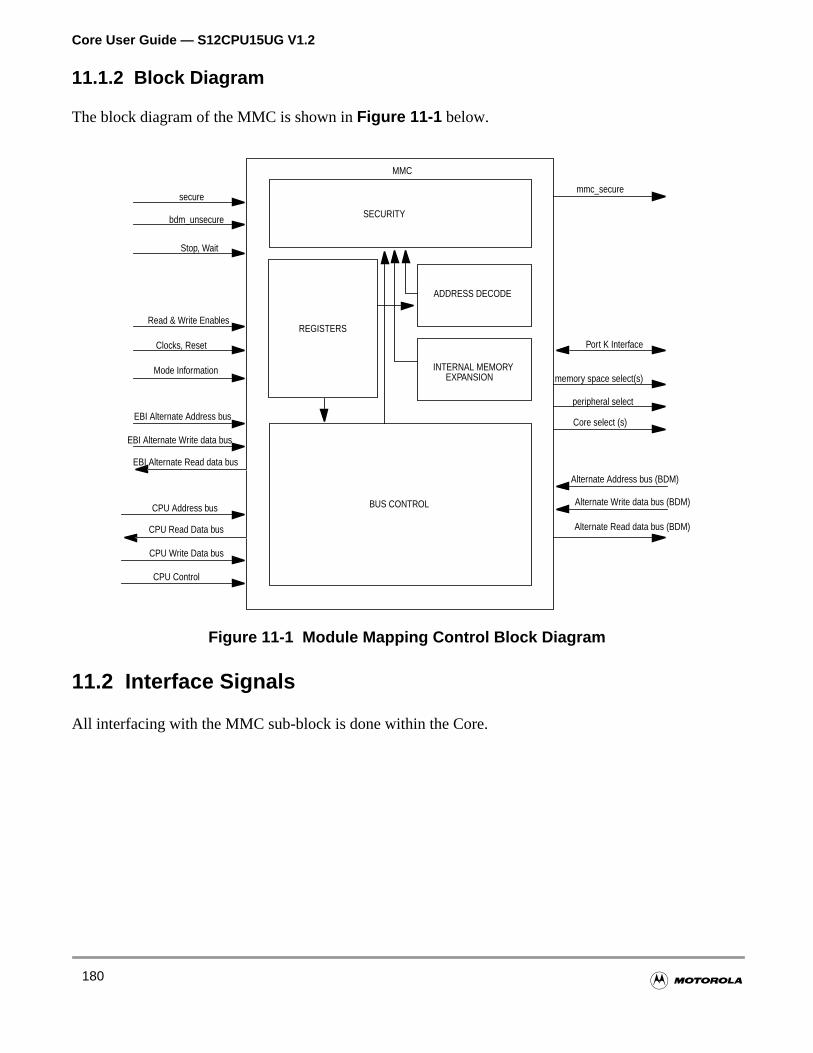
Core User Guide — S12CPU15UG V1.2
11.1.2 Block Diagram
The block diagram of the MMC is shown inFigure 11-1 below.
Figure 11-1 Module Mapping Control Block Diagram
11.2 Interface Signals
All interfacing with the MMC sub-block is done within the Core.
MMC
Mode Information
REGISTERS
CPU Write Data bus
CPU Address bus
CPU Control
Stop, Wait
ADDRESS DECODE
CPU Read Data bus
EBI Alternate Address bus
EBI Alternate Write data bus
EBI Alternate Read data bus
SECURITY
INTERNAL MEMORYEXPANSION
Clocks, Reset
Read & Write Enables
Alternate Address bus (BDM)
Alternate Write data bus (BDM)
Alternate Read data bus (BDM)
Core select (s)
Port K Interface
memory space select(s)
peripheral select
BUS CONTROL
secure
bdm_unsecure
mmc_secure
180
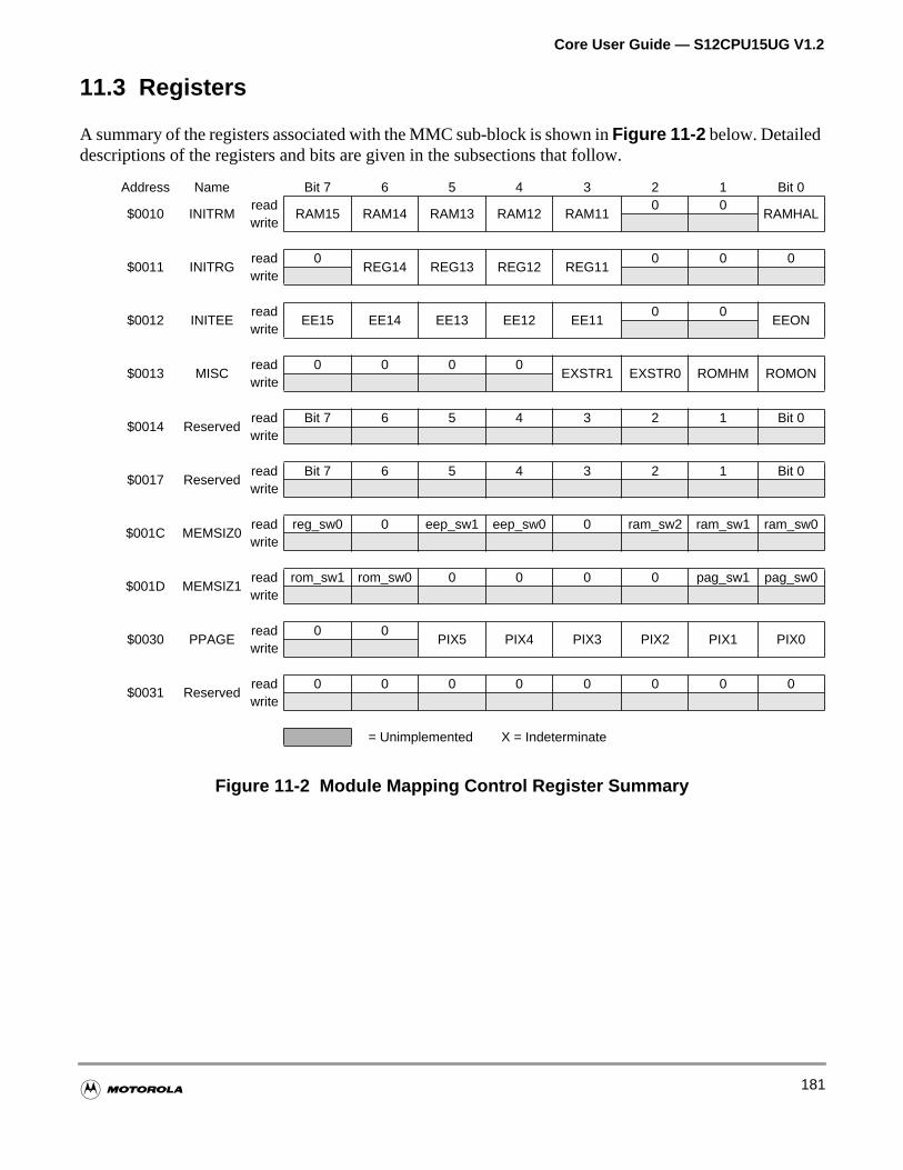
Core User Guide — S12CPU15UG V1.2
11.3 Registers
A summary of the registers associated with the MMC sub-block is shown inFigure 11-2 below. Detaileddescriptions of the registers and bits are given in the subsections that follow.
Figure 11-2 Module Mapping Control Register Summary
Address Name Bit 7 6 5 4 3 2 1 Bit 0
$0010 INITRMread
RAM15 RAM14 RAM13 RAM12 RAM110 0
RAMHALwrite
$0011 INITRGread 0
REG14 REG13 REG12 REG110 0 0
write
$0012 INITEEread
EE15 EE14 EE13 EE12 EE110 0
EEONwrite
$0013 MISCread 0 0 0 0
EXSTR1 EXSTR0 ROMHM ROMONwrite
$0014 Reservedread Bit 7 6 5 4 3 2 1 Bit 0write
$0017 Reservedread Bit 7 6 5 4 3 2 1 Bit 0write
$001C MEMSIZ0read reg_sw0 0 eep_sw1 eep_sw0 0 ram_sw2 ram_sw1 ram_sw0write
$001D MEMSIZ1read rom_sw1 rom_sw0 0 0 0 0 pag_sw1 pag_sw0write
$0030 PPAGEread 0 0
PIX5 PIX4 PIX3 PIX2 PIX1 PIX0write
$0031 Reservedread 0 0 0 0 0 0 0 0write
= Unimplemented X = Indeterminate
181
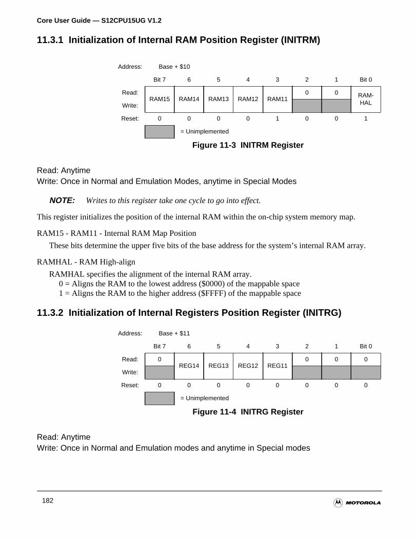
Core User Guide — S12CPU15UG V1.2
ay.
11.3.1 Initialization of Internal RAM Position Register (INITRM)
Read: AnytimeWrite: Once in Normal and Emulation Modes, anytime in Special Modes
NOTE: Writes to this register take one cycle to go into effect.
This register initializes the position of the internal RAM within the on-chip system memory map.
RAM15 - RAM11 - Internal RAM Map Position
These bits determine the upper five bits of the base address for the system’s internal RAM arr
RAMHAL - RAM High-align
RAMHAL specifies the alignment of the internal RAM array.0 = Aligns the RAM to the lowest address ($0000) of the mappable space1 = Aligns the RAM to the higher address ($FFFF) of the mappable space
11.3.2 Initialization of Internal Registers Position Register (INITRG)
Read: AnytimeWrite: Once in Normal and Emulation modes and anytime in Special modes
Address: Base + $10
Bit 7 6 5 4 3 2 1 Bit 0
Read:RAM15 RAM14 RAM13 RAM12 RAM11
0 0 RAM-HALWrite:
Reset: 0 0 0 0 1 0 0 1
= Unimplemented
Figure 11-3 INITRM Register
Address: Base + $11
Bit 7 6 5 4 3 2 1 Bit 0
Read: 0REG14 REG13 REG12 REG11
0 0 0
Write:
Reset: 0 0 0 0 0 0 0 0
= Unimplemented
Figure 11-4 INITRG Register
182
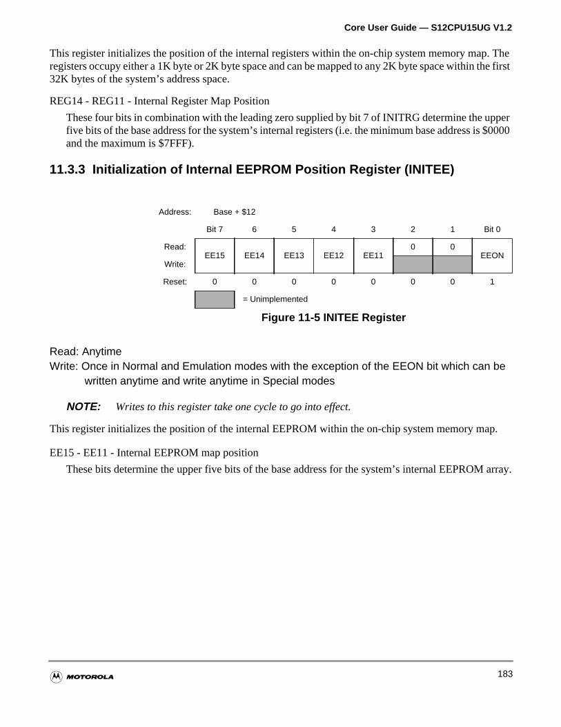
Core User Guide — S12CPU15UG V1.2
. Thehe first
pper$0000
p.
array.
This register initializes the position of the internal registers within the on-chip system memory mapregisters occupy either a 1K byte or 2K byte space and can be mapped to any 2K byte space within t32K bytes of the system’s address space.
REG14 - REG11 - Internal Register Map Position
These four bits in combination with the leading zero supplied by bit 7 of INITRG determine the ufive bits of the base address for the system’s internal registers (i.e. the minimum base address isand the maximum is $7FFF).
11.3.3 Initialization of Internal EEPROM Position Register (INITEE)
Read: AnytimeWrite: Once in Normal and Emulation modes with the exception of the EEON bit which can be
written anytime and write anytime in Special modes
NOTE: Writes to this register take one cycle to go into effect.
This register initializes the position of the internal EEPROM within the on-chip system memory ma
EE15 - EE11 - Internal EEPROM map position
These bits determine the upper five bits of the base address for the system’s internal EEPROM
Address: Base + $12
Bit 7 6 5 4 3 2 1 Bit 0
Read:EE15 EE14 EE13 EE12 EE11
0 0EEON
Write:
Reset: 0 0 0 0 0 0 0 1
= Unimplemented
Figure 11-5 INITEE Register
183
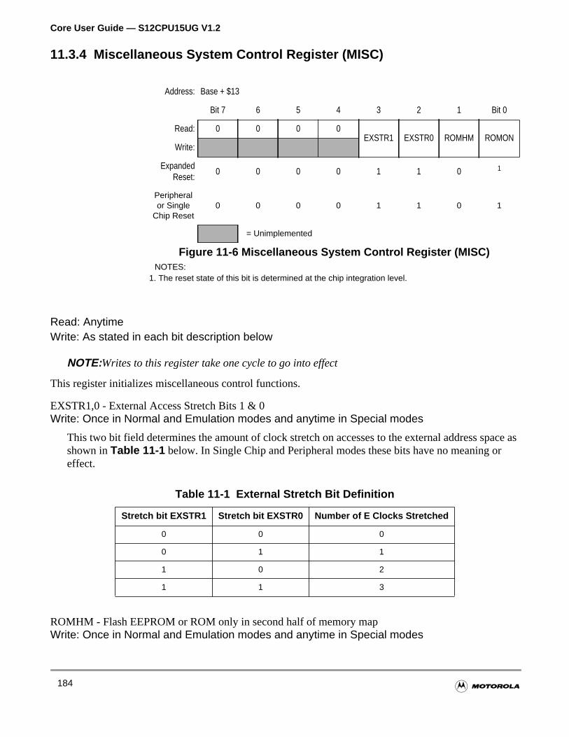
Core User Guide — S12CPU15UG V1.2
ace asor
11.3.4 Miscellaneous System Control Register (MISC)
Read: AnytimeWrite: As stated in each bit description below
NOTE:Writes to this register take one cycle to go into effect
This register initializes miscellaneous control functions.
EXSTR1,0 - External Access Stretch Bits 1 & 0Write: Once in Normal and Emulation modes and anytime in Special modes
This two bit field determines the amount of clock stretch on accesses to the external address spshown inTable 11-1 below. In Single Chip and Peripheral modes these bits have no meaning effect.
ROMHM - Flash EEPROM or ROM only in second half of memory mapWrite: Once in Normal and Emulation modes and anytime in Special modes
Address: Base + $13
Bit 7 6 5 4 3 2 1 Bit 0
Read: 0 0 0 0EXSTR1 EXSTR0 ROMHM ROMON
Write:
ExpandedReset:
0 0 0 0 1 1 0 1
NOTES:1. The reset state of this bit is determined at the chip integration level.
Peripheralor Single
Chip Reset0 0 0 0 1 1 0 1
= Unimplemented
Figure 11-6 Miscellaneous System Control Register (MISC)
Table 11-1 External Stretch Bit Definition
Stretch bit EXSTR1 Stretch bit EXSTR0 Number of E Clocks Stretched
0 0 0
0 1 1
1 0 2
1 1 3
184
Core User Guide — S12CPU15UG V1.2
ap.he
e
1 = Disables direct access to the Flash EEPROM or ROM in the lower half of the memory mThese physical locations of the Flash EEPROM or ROM can still be accessed through tProgram Page window.
0 = The fixed page(s) of Flash EEPROM or ROM in the lower half of the memory map can baccessed.
ROMON - Enable Flash EEPROM or ROMWrite: Once in Normal and Emulation modes and anytime in Special modes
This bit is used to enable the Flash EEPROM or ROM memory in the memory map.1 = Enables the Flash EEPROM or ROM in the memory map.0 = Disables the Flash EEPROM or ROM from the memory map.
11.3.5 Reserved Test Register Zero (MTST0)
Read: Anytime
Write: No effect - this register location is used for internal test purposes.
11.3.6 Reserved Test Register One (MTST1)
Read: Anytime
Write: No effect - this register location is used for internal test purposes.
Address: Base + $17
Read: 0 0 0 0 0 0 0 0
Write:
Reset: 0 0 0 0 0 0 0 0
= Unimplemented
Figure 11-7 Reserved Test Register Zero (MTST0)
Address: Base + $14
Read: 0 0 0 0 0 0 0 0
Write:
Reset: 0 0 0 1 0 0 0 0
= Unimplemented
Figure 11-8 Reserved Test Register One (MTST1)
185
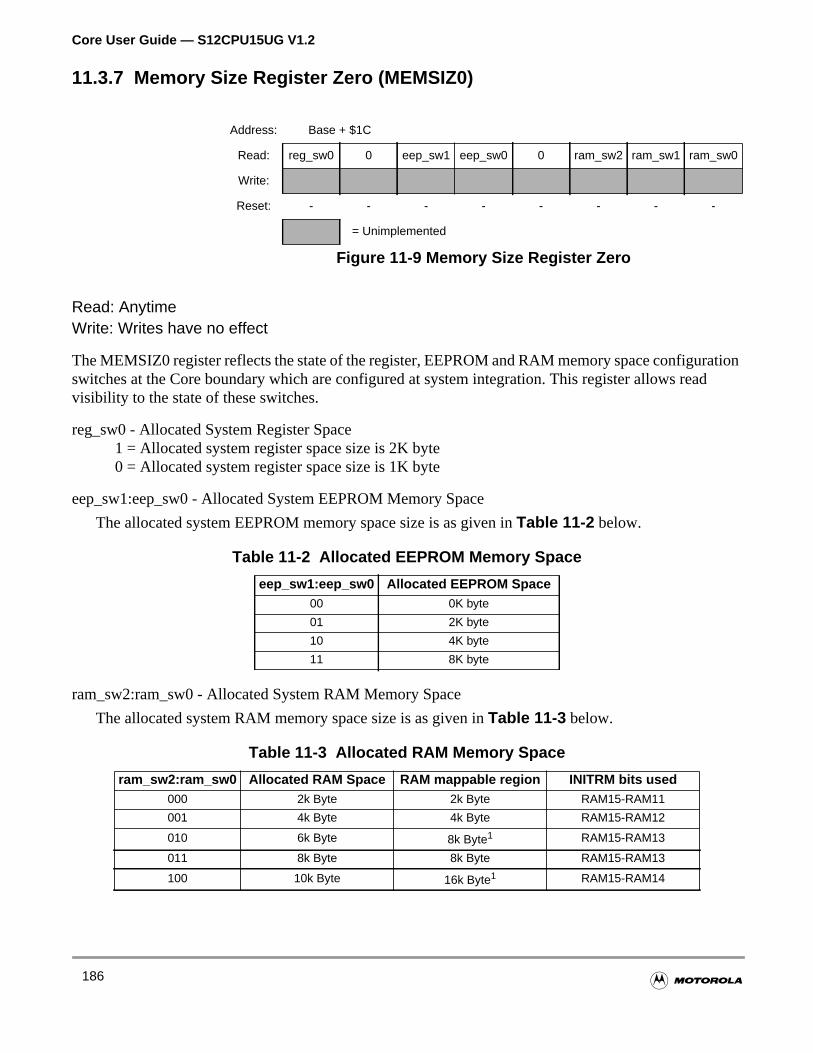
Core User Guide — S12CPU15UG V1.2
ationad
11.3.7 Memory Size Register Zero (MEMSIZ0)
Read: AnytimeWrite: Writes have no effect
The MEMSIZ0 register reflects the state of the register, EEPROM and RAM memory space configurswitches at the Core boundary which are configured at system integration. This register allows revisibility to the state of these switches.
reg_sw0 - Allocated System Register Space1 = Allocated system register space size is 2K byte0 = Allocated system register space size is 1K byte
eep_sw1:eep_sw0 - Allocated System EEPROM Memory Space
The allocated system EEPROM memory space size is as given inTable 11-2 below.
ram_sw2:ram_sw0 - Allocated System RAM Memory Space
The allocated system RAM memory space size is as given inTable 11-3 below.
Address: Base + $1C
Read: reg_sw0 0 eep_sw1 eep_sw0 0 ram_sw2 ram_sw1 ram_sw0
Write:
Reset: - - - - - - - -
= Unimplemented
Figure 11-9 Memory Size Register Zero
Table 11-2 Allocated EEPROM Memory Space
eep_sw1:eep_sw0 Allocated EEPROM Space00 0K byte
01 2K byte
10 4K byte
11 8K byte
Table 11-3 Allocated RAM Memory Space
ram_sw2:ram_sw0 Allocated RAM Space RAM mappable region INITRM bits used000 2k Byte 2k Byte RAM15-RAM11
001 4k Byte 4k Byte RAM15-RAM12
010 6k Byte 8k Byte1 RAM15-RAM13
011 8k Byte 8k Byte RAM15-RAM13
100 10k Byte 16k Byte1 RAM15-RAM14
186
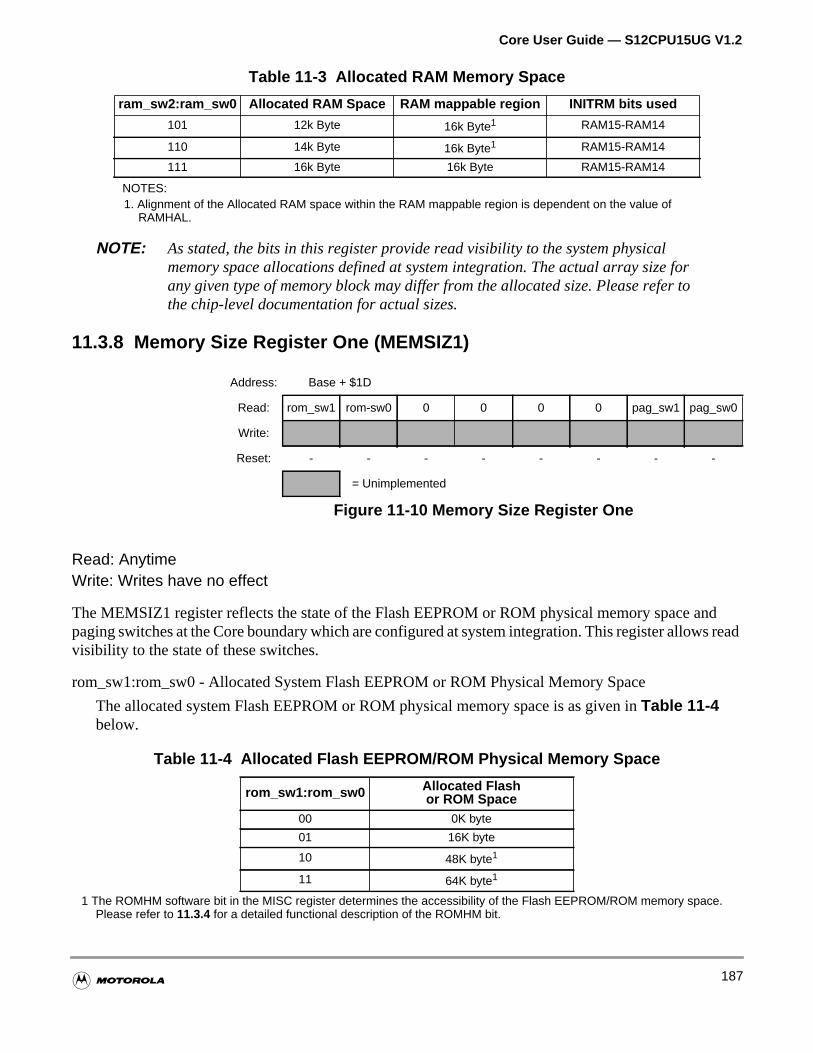
Core User Guide — S12CPU15UG V1.2
nds read
NOTE: As stated, the bits in this register provide read visibility to the system physicalmemory space allocations defined at system integration. The actual array size forany given type of memory block may differ from the allocated size. Please refer tothe chip-level documentation for actual sizes.
11.3.8 Memory Size Register One (MEMSIZ1)
Read: AnytimeWrite: Writes have no effect
The MEMSIZ1 register reflects the state of the Flash EEPROM or ROM physical memory space apaging switches at the Core boundary which are configured at system integration. This register allowvisibility to the state of these switches.
rom_sw1:rom_sw0 - Allocated System Flash EEPROM or ROM Physical Memory Space
The allocated system Flash EEPROM or ROM physical memory space is as given inTable 11-4below.
1 The ROMHM software bit in the MISC register determines the accessibility of the Flash EEPROM/ROM memory space.Please refer to 11.3.4 for a detailed functional description of the ROMHM bit.
101 12k Byte 16k Byte1 RAM15-RAM14
110 14k Byte 16k Byte1 RAM15-RAM14
111 16k Byte 16k Byte RAM15-RAM14
NOTES:1. Alignment of the Allocated RAM space within the RAM mappable region is dependent on the value of
RAMHAL.
Address: Base + $1D
Read: rom_sw1 rom-sw0 0 0 0 0 pag_sw1 pag_sw0
Write:
Reset: - - - - - - - -
= Unimplemented
Figure 11-10 Memory Size Register One
Table 11-4 Allocated Flash EEPROM/ROM Physical Memory Space
rom_sw1:rom_sw0 Allocated Flashor ROM Space
00 0K byte
01 16K byte
10 48K byte1
11 64K byte1
Table 11-3 Allocated RAM Memory Space
ram_sw2:ram_sw0 Allocated RAM Space RAM mappable region INITRM bits used
187
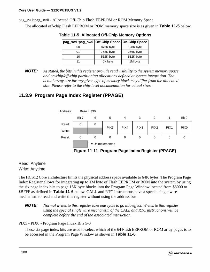
Core User Guide — S12CPU15UG V1.2
Pagesing0 to
s is to
pag_sw1:pag_sw0 - Allocated Off-Chip Flash EEPROM or ROM Memory Space
The allocated off-chip Flash EEPROM or ROM memory space size is as given inTable 11-5 below.
NOTE: As stated, the bits in this register provide read visibility to the system memory spaceand on-chip/off-chip partitioning allocations defined at system integration. Theactual array size for any given type of memory block may differ from the allocatedsize. Please refer to the chip-level documentation for actual sizes.
11.3.9 Program Page Index Register (PPAGE)
Read: AnytimeWrite: Anytime
The HCS12 Core architecture limits the physical address space available to 64K bytes. The ProgramIndex Register allows for integrating up to 1M byte of Flash EEPROM or ROM into the system by uthe six page index bits to page 16K byte blocks into the Program Page Window located from $800$BFFF as defined inTable 11-6 below. CALL and RTC instructions have a special single wiremechanism to read and write this register without using the address bus.
NOTE: Normal writes to this register take one cycle to go into effect. Writes to this registerusing the special single wire mechanism of the CALL and RTC instructions will becomplete before the end of the associated instruction.
PIX5 - PIX0 - Program Page Index Bits 5-0
These six page index bits are used to select which of the 64 Flash EEPROM or ROM array pagebe accessed in the Program Page Window as shown inTable 11-6 .
Table 11-5 Allocated Off-Chip Memory Options
pag_sw1:pag_sw0 Off-Chip Space On-Chip Space00 876K byte 128K byte
01 768K byte 256K byte
10 512K byte 512K byte
11 0K byte 1M byte
Address: Base + $30
Bit 7 6 5 4 3 2 1 Bit 0
Read: 0 0PIX5 PIX4 PIX3 PIX2 PIX1 PIX0
Write:
Reset: 0 0 0 0 0 0 0 0
= Unimplemented
Figure 11-11 Program Page Index Register (PPAGE)
188
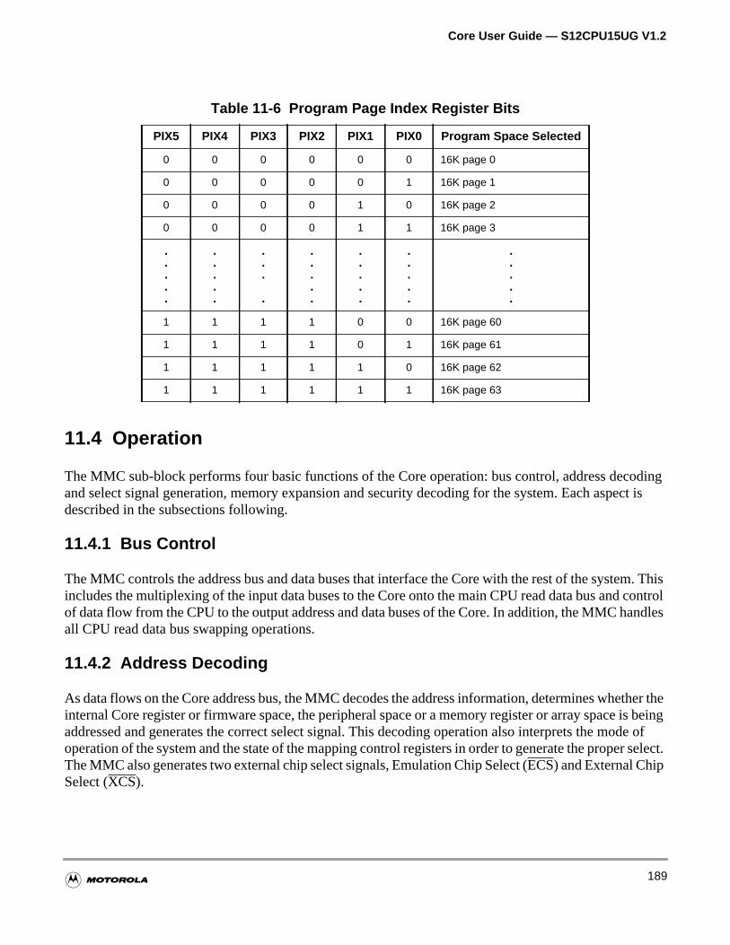
Core User Guide — S12CPU15UG V1.2
odingct is
m. Thiscontrolndles
ther thes beingde of
r select.
11.4 Operation
The MMC sub-block performs four basic functions of the Core operation: bus control, address decand select signal generation, memory expansion and security decoding for the system. Each aspedescribed in the subsections following.
11.4.1 Bus Control
The MMC controls the address bus and data buses that interface the Core with the rest of the systeincludes the multiplexing of the input data buses to the Core onto the main CPU read data bus andof data flow from the CPU to the output address and data buses of the Core. In addition, the MMC haall CPU read data bus swapping operations.
11.4.2 Address Decoding
As data flows on the Core address bus, the MMC decodes the address information, determines wheinternal Core register or firmware space, the peripheral space or a memory register or array space iaddressed and generates the correct select signal. This decoding operation also interprets the mooperation of the system and the state of the mapping control registers in order to generate the propeThe MMC also generates two external chip select signals, Emulation Chip Select (ECS) and External ChipSelect (XCS).
Table 11-6 Program Page Index Register Bits
PIX5 PIX4 PIX3 PIX2 PIX1 PIX0 Program Space Selected
0 0 0 0 0 0 16K page 0
0 0 0 0 0 1 16K page 1
0 0 0 0 1 0 16K page 2
0 0 0 0 1 1 16K page 3
.
.
.
.
.
.
.
.
.
.
.
.
.
.
.
.
.
.
.
.
.
.
.
.
.
.
.
.
.
.
.
.
.
.
1 1 1 1 0 0 16K page 60
1 1 1 1 0 1 16K page 61
1 1 1 1 1 0 16K page 62
1 1 1 1 1 1 16K page 63
189
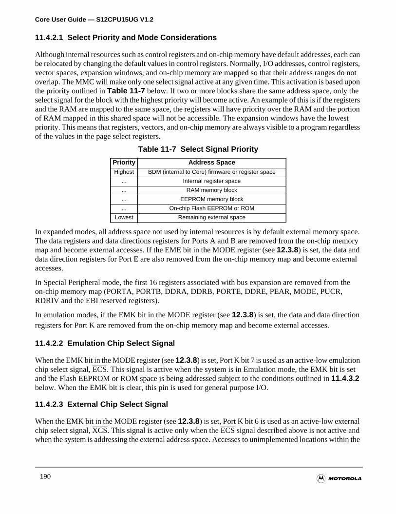
Core User Guide — S12CPU15UG V1.2
ach canisters,
s do notupon thetersortionestrdless
y space.emory
xternal
the
nset
aldithin the
11.4.2.1 Select Priority and Mode Considerations
Although internal resources such as control registers and on-chip memory have default addresses, ebe relocated by changing the default values in control registers. Normally, I/O addresses, control regvector spaces, expansion windows, and on-chip memory are mapped so that their address rangeoverlap. The MMC will make only one select signal active at any given time. This activation is basedthe priority outlined inTable 11-7 below. If two or more blocks share the same address space, onlyselect signal for the block with the highest priority will become active. An example of this is if the regisand the RAM are mapped to the same space, the registers will have priority over the RAM and the pof RAM mapped in this shared space will not be accessible. The expansion windows have the lowpriority. This means that registers, vectors, and on-chip memory are always visible to a program regaof the values in the page select registers.
In expanded modes, all address space not used by internal resources is by default external memorThe data registers and data directions registers for Ports A and B are removed from the on-chip mmap and become external accesses. If the EME bit in the MODE register (see12.3.8) is set, the data anddata direction registers for Port E are also removed from the on-chip memory map and become eaccesses.
In Special Peripheral mode, the first 16 registers associated with bus expansion are removed fromon-chip memory map (PORTA, PORTB, DDRA, DDRB, PORTE, DDRE, PEAR, MODE, PUCR,RDRIV and the EBI reserved registers).
In emulation modes, if the EMK bit in the MODE register (see12.3.8) is set, the data and data directionregisters for Port K are removed from the on-chip memory map and become external accesses.
11.4.2.2 Emulation Chip Select Signal
When the EMK bit in the MODE register (see12.3.8) is set, Port K bit 7 is used as an active-low emulatiochip select signal,ECS. This signal is active when the system is in Emulation mode, the EMK bit is and the Flash EEPROM or ROM space is being addressed subject to the conditions outlined in11.4.3.2below. When the EMK bit is clear, this pin is used for general purpose I/O.
11.4.2.3 External Chip Select Signal
When the EMK bit in the MODE register (see12.3.8) is set, Port K bit 6 is used as an active-low externchip select signal,XCS. This signal is active only when theECS signal described above is not active anwhen the system is addressing the external address space. Accesses to unimplemented locations w
Table 11-7 Select Signal Priority
Priority Address SpaceHighest BDM (internal to Core) firmware or register space
... Internal register space
... RAM memory block
... EEPROM memory block
... On-chip Flash EEPROM or ROM
Lowest Remaining external space
190
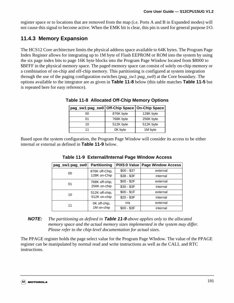
Core User Guide — S12CPU15UG V1.2
s) willse I/O.
Pagesing0 toory or
n
ther
PAGE
register space or to locations that are removed from the map (i.e. Ports A and B in Expanded modenot cause this signal to become active. When the EMK bit is clear, this pin is used for general purpo
11.4.3 Memory Expansion
The HCS12 Core architecture limits the physical address space available to 64K bytes. The ProgramIndex Register allows for integrating up to 1M byte of Flash EEPROM or ROM into the system by uthe six page index bits to page 16K byte blocks into the Program Page Window located from $800$BFFF in the physical memory space. The paged memory space can consist of solely on-chip mema combination of on-chip and off-chip memory. This partitioning is configured at system integratiothrough the use of the paging configuration switches (pag_sw1:pag_sw0) at the Core boundary. Theoptions available to the integrator are as given inTable 11-8 below (this table matchesTable 11-5 butis repeated here for easy reference).
Based upon the system configuration, the Program Page Window will consider its access to be eiinternal or external as defined inTable 11-9 below.
NOTE: The partitioning as defined inTable 11-9 above applies only to the allocatedmemory space and the actual memory sizes implemented in the system may differ.Please refer to the chip-level documentation for actual sizes.
The PPAGE register holds the page select value for the Program Page WIndow. The value of the Pregister can be manipulated by normal read and write instructions as well as the CALL and RTCinstructions.
Table 11-8 Allocated Off-Chip Memory Options
pag_sw1:pag_sw0 Off-Chip Space On-Chip Space00 876K byte 128K byte
01 768K byte 256K byte
10 512K byte 512K byte
11 0K byte 1M byte
Table 11-9 External/Internal Page Window Access
pag_sw1:pag_sw0 Partitioning PIX5:0 Value Page Window Access
00876K off-Chip,128K on-Chip
$00 - $37 external
$38 - $3F internal
01768K off-chip,256K on-chip
$00 - $2F external
$30 - $3F internal
10512K off-chip,512K on-chip
$00 - $1F external
$20 - $3F internal
110K off-chip,1M on-chip
n/a external
$00 - $3F internal
191
Core User Guide — S12CPU15UG V1.2
of theto make
ceptiones that
is
nsionhere
es andalue toeed
), and
e new
ALL
odein the
newhe newdiate
AGEter the
Control registers, vector spaces and a portion of on-chip memory are located in unpaged portions64K byte physical address space. The stack and I/O addresses should also be in unpaged memorythem accessible from any page.
The starting address of a service routine must be located in unpaged memory because the 16-bit exvectors cannot point to addresses in paged memory. However, a service routine can call other routinare in paged memory. The upper 16K byte block of memory space ($C000-$FFFF) is unpaged. Itrecommended that all reset and interrupt vectors point to locations in this area.
11.4.3.1 CALL and Return from Call Instructions
CALL and RTC are uninterruptable instructions that automate page switching in the program expawindow. CALL is similar to a JSR instruction, but the subroutine that is called can be located anywin the normal 64K byte address space or on any page of program expansion memory. CALL calculatstacks a return address, stacks the current PPAGE value, and writes a new instruction-supplied vPPAGE. The PPAGE value controls which of the 64 possible pages is visible through the 16K bytexpansion window in the 64K byte memory map. Execution then begins at the address of the callsubroutine.
During the execution of a CALL instruction, the CPU:
• Writes the old PPAGE value into an internal temporary register and writes the newinstruction-supplied PPAGE value into the PPAGE register.
• Calculates the address of the next instruction after the CALL instruction (the return addresspushes this 16-bit value onto the stack.
• Pushes the old PPAGE value onto the stack.
• Calculates the effective address of the subroutine, refills the queue, and begins execution at thaddress on the selected page of the expansion window.
This sequence is uninterruptable; there is no need to inhibit interrupts during CALL execution. A Ccan be performed from any address in memory to any other address.
The PPAGE value supplied by the instruction is part of the effective address. For all addressing mvariations except indexed-indirect modes, the new page value is provided by an immediate operandinstruction. In indexed-indirect variations of CALL, a pointer specifies memory locations where thepage value and the address of the called subroutine are stored. Using indirect addressing for both tpage value and the address within the page allows values calculated at run time rather than immevalues that must be known at the time of assembly.
The RTC instruction terminates subroutines invoked by a CALL instruction. RTC unstacks the PPvalue and the return address and refills the queue. Execution resumes with the next instruction afCALL.
During the execution of an RTC instruction, the CPU:
• Pulls the old PPAGE value from the stack
• Pulls the 16-bit return address from the stack and loads it into the PC
• Writes the old PPAGE value into the PPAGE register
192
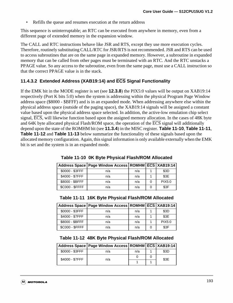
Core User Guide — S12CPU15UG V1.2
a
s.used
xpandedcks ation so
indowithin thenstant
selectbyte
MK
• Refills the queue and resumes execution at the return address
This sequence is uninterruptable; an RTC can be executed from anywhere in memory, even fromdifferent page of extended memory in the expansion window.
The CALL and RTC instructions behave like JSR and RTS, except they use more execution cycleTherefore, routinely substituting CALL/RTC for JSR/RTS is not recommended. JSR and RTS can beto access subroutines that are on the same page in expanded memory. However, a subroutine in ememory that can be called from other pages must be terminated with an RTC. And the RTC unstaPPAGE value. So any access to the subroutine, even from the same page, must use a CALL instructhat the correct PPAGE value is in the stack.
11.4.3.2 Extended Address (XAB19:14) and ECS Signal Functionality
If the EMK bit in the MODE register is set (see12.3.8) the PIX5:0 values will be output on XAB19:14respectively (Port K bits 5:0) when the system is addressing within the physical Program Page Waddress space ($8000 - $BFFF) and is in an expanded mode. When addressing anywhere else wphysical address space (outside of the paging space), the XAB19:14 signals will be assigned a covalue based upon the physical address space selected. In addition, the active-low emulation chipsignal,ECS, will likewise function based upon the assigned memory allocation. In the cases of 48Kand 64K byte allocated physical Flash/ROM space, the operation of theECS signal will additionallydepend upon the state of the ROMHM bit (see11.3.4) in the MISC register.Table 11-10 , Table 11-11 ,Table 11-12 andTable 11-13 below summarize the functionality of these signals based upon theallocated memory configuration. Again, this signal information is only available externally when the Ebit is set and the system is in an expanded mode.
Table 11-10 0K Byte Physical Flash/ROM Allocated
Address Space Page Window Access ROMHM ECS XAB19:14$0000 - $3FFF n/a n/a 1 $3D
$4000 - $7FFF n/a n/a 1 $3E
$8000 - $BFFF n/a n/a 0 PIX5:0
$C000 - $FFFF n/a n/a 0 $3F
Table 11-11 16K Byte Physical Flash/ROM Allocated
Address Space Page Window Access ROMHM ECS XAB19:14$0000 - $3FFF n/a n/a 1 $3D
$4000 - $7FFF n/a n/a 1 $3E
$8000 - $BFFF n/a n/a 1 PIX5:0
$C000 - $FFFF n/a n/a 0 $3F
Table 11-12 48K Byte Physical Flash/ROM Allocated
Address Space Page Window Access ROMHM ECS XAB19:14$0000 - $3FFF n/a n/a 1 $3D
$4000 - $7FFF n/a0 0
$3E1 1
193
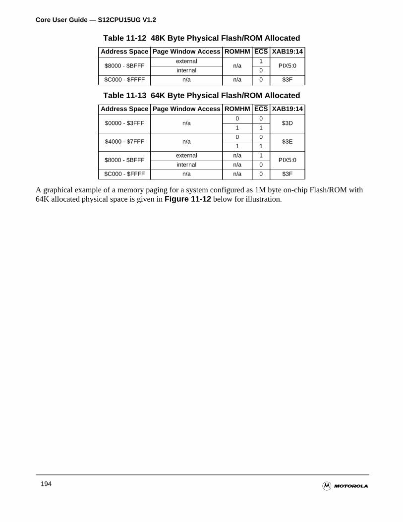
Core User Guide — S12CPU15UG V1.2
with
A graphical example of a memory paging for a system configured as 1M byte on-chip Flash/ROM64K allocated physical space is given inFigure 11-12 below for illustration.$8000 - $BFFFexternal
n/a1
PIX5:0internal 0
$C000 - $FFFF n/a n/a 0 $3F
Table 11-13 64K Byte Physical Flash/ROM Allocated
Address Space Page Window Access ROMHM ECS XAB19:14
$0000 - $3FFF n/a0 0
$3D1 1
$4000 - $7FFF n/a0 0
$3E1 1
$8000 - $BFFFexternal n/a 1
PIX5:0internal n/a 0
$C000 - $FFFF n/a n/a 0 $3F
Table 11-12 48K Byte Physical Flash/ROM Allocated
Address Space Page Window Access ROMHM ECS XAB19:14
194
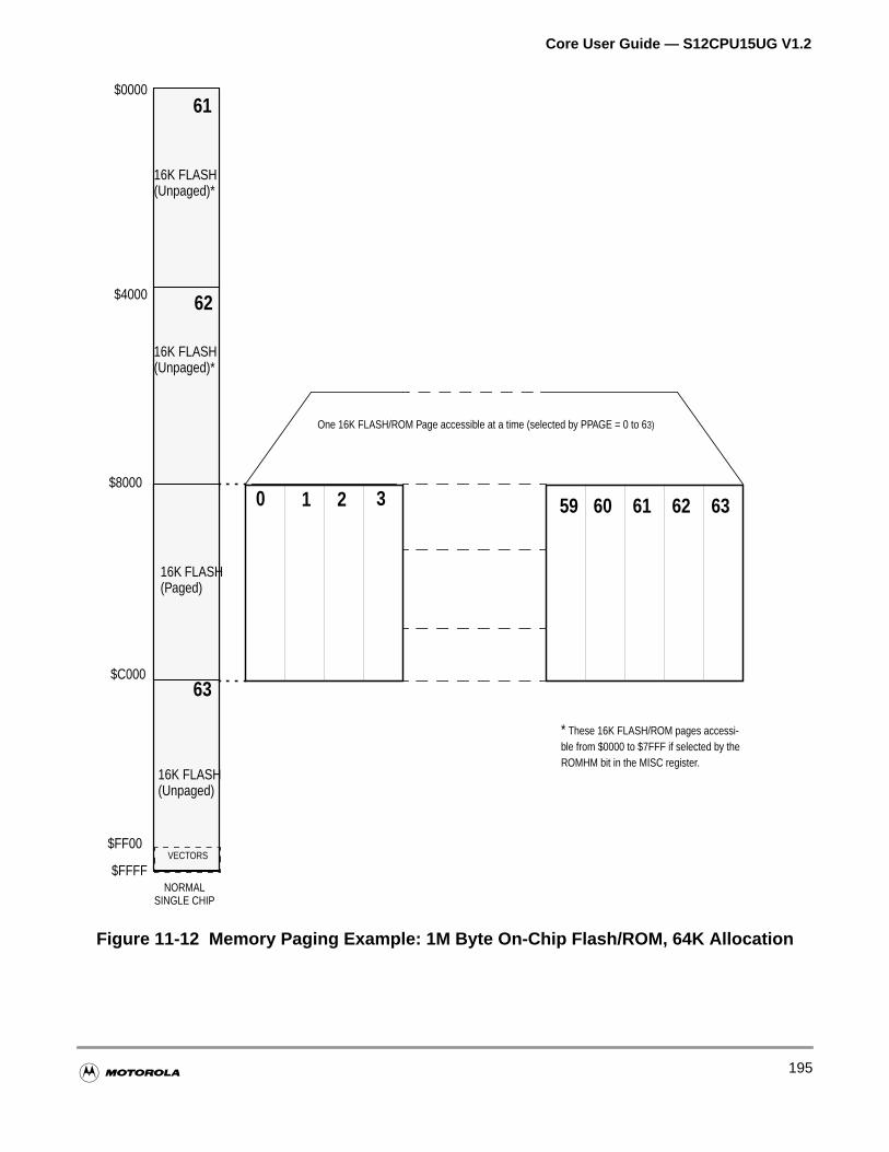
Core User Guide — S12CPU15UG V1.2
Figure 11-12 Memory Paging Example: 1M Byte On-Chip Flash/ROM, 64K Allocation
* These 16K FLASH/ROM pages accessi-ble from $0000 to $7FFF if selected by theROMHM bit in the MISC register.
NORMALSINGLE CHIP
VECTORS
One 16K FLASH/ROM Page accessible at a time (selected by PPAGE = 0 to 63)
$0000
$8000
$FF00
$FFFF
16K FLASH(Unpaged)
$4000
$C000
16K FLASH(Unpaged)*
16K FLASH(Paged)
59
62
63
60 61 62 630 1 2 3
61
16K FLASH(Unpaged)*
195
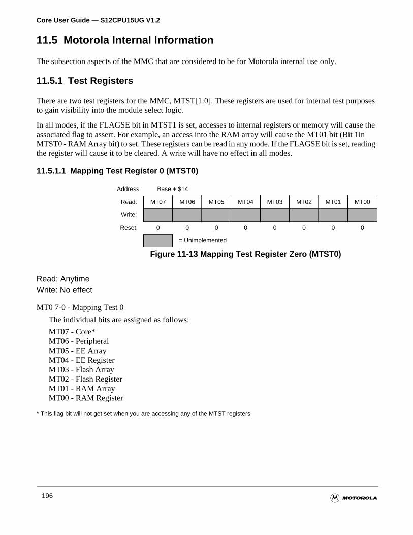
Core User Guide — S12CPU15UG V1.2
poses
e the 1inding
11.5 Motorola Internal Information
The subsection aspects of the MMC that are considered to be for Motorola internal use only.
11.5.1 Test Registers
There are two test registers for the MMC, MTST[1:0]. These registers are used for internal test purto gain visibility into the module select logic.
In all modes, if the FLAGSE bit in MTST1 is set, accesses to internal registers or memory will causassociated flag to assert. For example, an access into the RAM array will cause the MT01 bit (BitMTST0 - RAM Array bit) to set. These registers can be read in any mode. If the FLAGSE bit is set, reathe register will cause it to be cleared. A write will have no effect in all modes.
11.5.1.1 Mapping Test Register 0 (MTST0)
Read: AnytimeWrite: No effect
MT0 7-0 - Mapping Test 0
The individual bits are assigned as follows:
MT07 - Core*MT06 - PeripheralMT05 - EE ArrayMT04 - EE RegisterMT03 - Flash ArrayMT02 - Flash RegisterMT01 - RAM ArrayMT00 - RAM Register
* This flag bit will not get set when you are accessing any of the MTST registers
Address: Base + $14
Read: MT07 MT06 MT05 MT04 MT03 MT02 MT01 MT00
Write:
Reset: 0 0 0 0 0 0 0 0
= Unimplemented
Figure 11-13 Mapping Test Register Zero (MTST0)
196
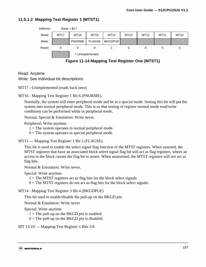
Core User Guide — S12CPU15UG V1.2
t the
, there ant act as
11.5.1.2 Mapping Test Register 1 (MTST1)
Read: AnytimeWrite: See individual bit descriptions
MT17 - Unimplemented (reads back zero)
MT16 - Mapping Test Register 1 Bit 6 (PNORME).
Normally, the system will enter peripheral mode and be in a special mode. Setting this bit will pusystem into normal peripheral mode. This is so that testing of register normal mode read/writeconditions can be performed while in peripheral mode.
Normal, Special & Emulation: Write never.
Peripheral: Write anytime.1 = The system operates in normal peripheral mode.0 = The system operates in special peripheral mode.
MT15 — Mapping Test Register 1 Bit 5 (FLAGSE).
This bit is used to enable the select signal flag function of the MTST registers. When assertedMTST registers that have an associated block select signal flag bit will act as flag registers, wheaccess to the block causes the flag bit to assert. When unasserted, the MTST registers will noflag bits.
Normal & Emulation: Write never.
Special: Write anytime.1 = The MTST registers act as flag bits for the block select signals.0 = The MTST registers do not act as flag bits for the block select signals.
MT14 - Mapping Test Register 3 Bit 4 (BKGDPUE)
This bit used to enable/disable the pull-up on the BKGD pin.
Normal & Emulation: Write never
Special: Write anytime1 = The pull-up on the BKGD pin is enabled.0 = The pull-up on the BKGD pin is disabled.
MT 13-10 — Mapping Test Register 1 Bits 3:0
Address: Base + $17
Read: MT17 MT16 MT15 MT14 MT13 MT12 MT11 MT10
Write: PNORME FLAGSE BKGDPUE
Reset: 0 0 0 1 0 0 0 0
= Unimplemented
Figure 11-14 Mapping Test Register One (MTST1)
197
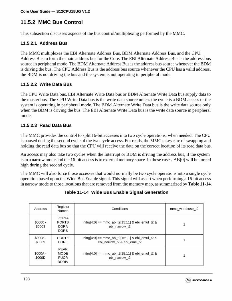
Core User Guide — S12CPU15UG V1.2
ss buse BDMddress,
ta toor theonlyeral
CPUing andta bus.
ystemforced
cycleccess
11.5.2 MMC Bus Control
This subsection discusses aspects of the bus control/multiplexing performed by the MMC.
11.5.2.1 Address Bus
The MMC multiplexes the EBI Alternate Address Bus, BDM Alternate Address Bus, and the CPUAddress Bus to form the main address bus for the Core. The EBI Alternate Address Bus is the addresource in peripheral mode. The BDM Alternate Address Bus is the address bus source whenever this driving the bus. The CPU Address Bus is the address bus source whenever the CPU has a valid athe BDM is not driving the bus and the system is not operating in peripheral mode.
11.5.2.2 Write Data Bus
The CPU Write Data bus, EBI Alternate Write Data bus or BDM Alternate Write Data bus supply dathe master bus. The CPU Write Data bus is the write data source unless the cycle is a BDM accesssystem is operating in peripheral mode. The BDM Alternate Write Data bus is the write data sourcewhen the BDM is driving the bus. The EBI Alternate Write Data bus is the write data source in periphmode.
11.5.2.3 Read Data Bus
The MMC provides the control to split 16-bit accesses into two cycle operations, when needed. Theis paused during the second cycle of the two cycle access. For reads, the MMC takes care of swappholding the read data bus so that the CPU will receive the data on the correct location of its read da
An access may also take two cycles when the Interrupt or BDM is driving the address bus, if the sis in a narrow mode and the 16-bit access is to external memory space. In these cases, AB[0] will behigh during the second cycle.
The MMC will also force those accesses that would normally be two cycle operations into a singleoperation based upon the Wide Bus Enable signal. This signal will assert when performing a 16-bit ain narrow mode to those locations that are removed from the memory map, as summarized byTable 11-14.
Table 11-14 Wide Bus Enable Signal Generation
AddressRegisterNames
Conditions mmc_widebuse_t2
$0000 -$0003
PORTAPORTBDDRADDRB
initrg[4:0] == mmc_ab_t2[15:11] & ebi_emul_t2 &ebi_narrow_t2
1
$0008 -$0009
PORTEDDRE
initrg[4:0] == mmc_ab_t2[15:11] & ebi_emul_t2 &ebi_narrow_t2 & ebi_eme_t2
1
$000A -$000D
PEARMODEPUCRRDRIV
initrg[4:0] == mmc_ab_t2[15:11] & ebi_emul_t2 &ebi_narrow_t2
1
198
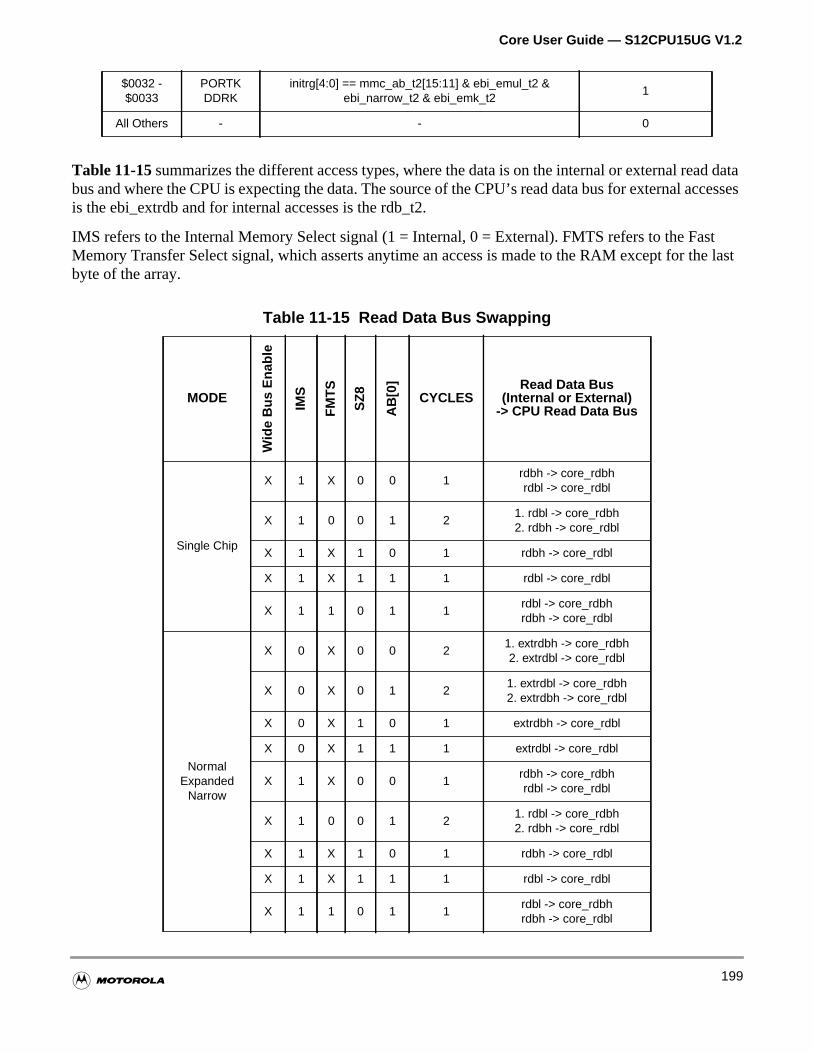
Core User Guide — S12CPU15UG V1.2
d dataccesses
sthe last
Table 11-15summarizes the different access types, where the data is on the internal or external reabus and where the CPU is expecting the data. The source of the CPU’s read data bus for external ais the ebi_extrdb and for internal accesses is the rdb_t2.
IMS refers to the Internal Memory Select signal (1 = Internal, 0 = External). FMTS refers to the FaMemory Transfer Select signal, which asserts anytime an access is made to the RAM except for tbyte of the array.
$0032 -$0033
PORTKDDRK
initrg[4:0] == mmc_ab_t2[15:11] & ebi_emul_t2 &ebi_narrow_t2 & ebi_emk_t2
1
All Others - - 0
Table 11-15 Read Data Bus Swapping
MODE
Wid
e B
us E
nabl
e
IMS
FM
TS
SZ
8
AB
[0]
CYCLESRead Data Bus
(Internal or External)-> CPU Read Data Bus
Single Chip
X 1 X 0 0 1rdbh -> core_rdbhrdbl -> core_rdbl
X 1 0 0 1 21. rdbl -> core_rdbh2. rdbh -> core_rdbl
X 1 X 1 0 1 rdbh -> core_rdbl
X 1 X 1 1 1 rdbl -> core_rdbl
X 1 1 0 1 1rdbl -> core_rdbhrdbh -> core_rdbl
NormalExpanded
Narrow
X 0 X 0 0 21. extrdbh -> core_rdbh2. extrdbl -> core_rdbl
X 0 X 0 1 21. extrdbl -> core_rdbh2. extrdbh -> core_rdbl
X 0 X 1 0 1 extrdbh -> core_rdbl
X 0 X 1 1 1 extrdbl -> core_rdbl
X 1 X 0 0 1rdbh -> core_rdbhrdbl -> core_rdbl
X 1 0 0 1 21. rdbl -> core_rdbh2. rdbh -> core_rdbl
X 1 X 1 0 1 rdbh -> core_rdbl
X 1 X 1 1 1 rdbl -> core_rdbl
X 1 1 0 1 1rdbl -> core_rdbhrdbh -> core_rdbl
199
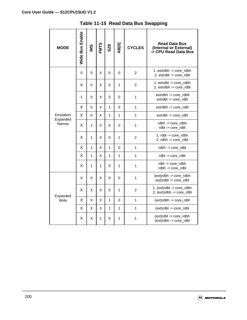
Core User Guide — S12CPU15UG V1.2
EmulationExpanded
Narrow
0 0 X 0 0 21. extrdbh -> core_rdbh2. extrdbl -> core_rdbl
X 0 X 0 1 21. extrdbl -> core_rdbh2. extrdbh -> core_rdbl
1 0 X 0 0 1 extrdbh -> core_rdbhextrdbl -> core_rdbl
X 0 X 1 0 1 extrdbh -> core_rdbl
X 0 X 1 1 1 extrdbl -> core_rdbl
X 1 X 0 0 1rdbh -> core_rdbhrdbl -> core_rdbl
X 1 0 0 1 21. rdbl -> core_rdbh2. rdbh -> core_rdbl
X 1 X 1 0 1 rdbh -> core_rdbl
X 1 X 1 1 1 rdbl -> core_rdbl
X 1 1 0 1 1rdbl -> core_rdbhrdbh -> core_rdbl
ExpandedWide
X X X 0 0 1(ext)rdbh -> core_rdbh(ext)rdbl -> core_rdbl
X X 0 0 1 21. (ext)rdbl -> core_rdbh2. (ext)rdbh -> core_rdbl
X X X 1 0 1 (ext)rdbh -> core_rdbl
X X X 1 1 1 (ext)rdbl -> core_rdbl
X X 1 0 1 1(ext)rdbl -> core_rdbh(ext)rdbh -> core_rdbl
Table 11-15 Read Data Bus Swapping
MODE
Wid
e B
us E
nabl
e
IMS
FM
TS
SZ
8
AB
[0]
CYCLESRead Data Bus
(Internal or External)-> CPU Read Data Bus
200
Core User Guide — S12CPU15UG V1.2
k of
registerst
Section 12 Multiplexed External Bus Interface (MEBI)
This section describes the functionality of the Multiplexed External Bus Interface (MEBI) sub-blocthe Core.
12.1 Overview
The MEBI sub-block of the Core serves to provide access and/or visibility to internal Core datamanipulation operations including timing reference information at the external boundary of the Coand/or system. Depending upon the system operating mode and the state of bits within the control reof the MEBI, the internal 16-bit read and write data operations will be represented in 8-bit or 16-biaccesses externally. Using control information from other blocks within the system, the MEBI willdetermine the appropriate type of data access to be generated.
12.1.1 Features
• External bus controller with four 8-bit ports (A,B, E and K)
• Data and data direction registers for ports A, B E and K when used as general purpose I/O
• Control register to enable/disable alternate functions on Port E and Port K
• Mode control register
• Control register to enable/disable pullups on Ports A, B, E and K
• Control register to enable/disable reduced output drive on Ports A, B, E and K
• Control register to configure external clock behavior
• Control register to configureIRQ pin operation
• Logic to capture and synchronize external interrupt pin inputs
201
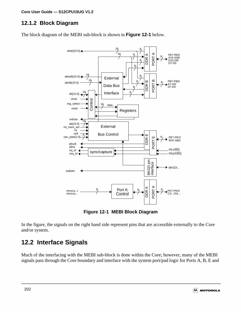
Core User Guide — S12CPU15UG V1.2
Core
EBIE and
12.1.2 Block Diagram
The block diagram of the MEBI sub-block is shown inFigure 12-1 below.
Figure 12-1 MEBI Block Diagram
In the figure, the signals on the right hand side represent pins that are accessible externally to theand/or system.
12.2 Interface Signals
Much of the interfacing with the MEBI sub-block is done within the Core; however, many of the Msignals pass through the Core boundary and interface with the system port/pad logic for Ports A, B,
Con
trol
External
Registers
BK
GD
pin
inte
rfac
eP
OR
T K
PO
RT
EP
OR
T A
DD
R K
DD
R E
DD
R A
PO
RT
B
DD
R B
Interface
Data Bus
External
Bus Control
8
8
6
8
16
Port KControl
16
16 data
8
8
8
8
8
8
8
8
8
16
16
16
16
8
2
PA7-PA0/A15-A08/D15-D8/D7-D0
PB7-PB0/A7-A0/D7-D0
PE7-PE2/(bus sigs)
PE1/IRQPE0/XIRQ
BKGD/...
PK7-PK0/CS.../XA...
mmccs.../mmcxa...
extbdm
altsz8altrwirq_t4xirq_t4
ab[15:0]int_mem_sel
rwsz8
cpu_pipe[1:0]
mdrste
db[15:0]
clock
reg_select
reset
altab[15:0]
altwdb[15:0]
altrdb[15:0]
sync/capture
202
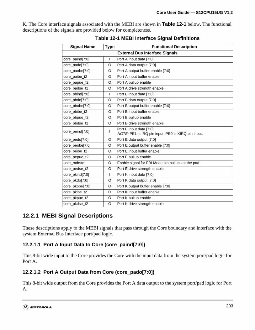
Core User Guide — S12CPU15UG V1.2
ith the
ic for
Port
K. The Core interface signals associated with the MEBI are shown inTable 12-1 below. The functionaldescriptions of the signals are provided below for completeness.
12.2.1 MEBI Signal Descriptions
These descriptions apply to the MEBI signals that pass through the Core boundary and interface wsystem External Bus Interface port/pad logic.
12.2.1.1 Port A Input Data to Core (core_paind[7:0])
This 8-bit wide input to the Core provides the Core with the input data from the system port/pad logPort A.
12.2.1.2 Port A Output Data from Core (core_pado[7:0])
This 8-bit wide output from the Core provides the Port A data output to the system port/pad logic forA.
Table 12-1 MEBI Interface Signal Definitions
Signal Name Type Functional Description
External Bus Interface Signalscore_paind[7:0] I Port A input data [7:0]
core_pado[7:0] O Port A data output [7:0]
core_paobe[7:0] O Port A output buffer enable [7:0]
core_paibe_t2 O Port A input buffer enable
core_papue_t2 O Port A pullup enable
core_padse_t2 O Port A drive strength enable
core_pbind[7:0] I Port B input data [7:0]
core_pbdo[7:0] O Port B data output [7:0]
core_pbobe[7:0] O Port B output buffer enable [7:0]
core_pbibe_t2 O Port B input buffer enable
core_pbpue_t2 O Port B pullup enable
core_pbdse_t2 O Port B drive strength enable
core_peind[7:0] IPort E input data [7:0]NOTE: PE1 is IRQ pin input; PE0 is XIRQ pin input.
core_pedo[7:0] O Port E data output [7:0]
core_peobe[7:0] O Port E output buffer enable [7:0]
core_peibe_t2 O Port E input buffer enable
core_pepue_t2 O Port E pullup enable
core_mdrste O Enable signal for EBI Mode pin pullups at the pad
core_pedse_t2 O Port E drive strength enable
core_pkind[7:0] I Port K input data [7:0]
core_pkdo[7:0] O Port K data output [7:0]
core_pkobe[7:0] O Port K output buffer enable [7:0]
core_pkibe_t2 O Port K input buffer enable
core_pkpue_t2 O Port K pullup enable
core_pkdse_t2 O Port K drive strength enable
203
Core User Guide — S12CPU15UG V1.2
m
logic
ic for
ed
ic for
Port
m
logic
in the
rive
12.2.1.3 Port A output buffer enable from Core (core_paobe[7:0])
This 8-bit wide output from the Core provides the bit-by-bit output buffer enable signal to the systeport/pad logic for Port A.
12.2.1.4 Port A input buffer enable from Core (core_paibe_t2)
This single bit output from the Core provides the input buffer enable signal to the system port/padfor Port A.
12.2.1.5 Port A pullup enable from Core (core_papue_t2)
This single bit output from the Core indicates that the pullup devices within the system port/pad logPort A should be enabled for all Port A pins.
12.2.1.6 Port A drive strength enable from Core (core_padse_t2)
This single bit output from the Core indicates whether all Port A pins will operate with full or reducdrive strength.
12.2.1.7 Port B Input Data to Core (core_pbind[7:0])
This 8-bit wide input to the Core provides the Core with the input data from the system port/pad logPort B.
12.2.1.8 Port B Output Data from Core (core_pbdo[7:0])
This 8-bit wide output from the Core provides the Port B data output to the system port/pad logic forB.
12.2.1.9 Port B output buffer enable from Core (core_pbobe[7:0])
This 8-bit wide output from the Core provides the bit-by-bit output buffer enable signal to the systeport/pad logic for Port B.
12.2.1.10 Port B input buffer enable from Core (core_pbibe_t2)
This single bit output from the Core provides the input buffer enable signal to the system port/padfor Port B.
12.2.1.11 Port B pullup enable from Core (core_pbpue_t2)
When asserted (logic 1), this single bit output from the Core indicates that the pullup devices withsystem port/pad logic for Port B should be enabled for all Port B pins.
12.2.1.12 Port B drive strength enable from Core (core_pbdse_t2)
This single bit output from the Core indicates whether all Port B pins will operate with full or reduced dstrength.
204
Core User Guide — S12CPU15UG V1.2
ic for
ort E.
m
logic
t/padins.
ic for
rive
ic for
Port
12.2.1.13 Port E Input Data to Core (core_peind[7:0])
This 8-bit wide input to the Core provides the Core with the input data from the system port/pad logPort E. When the system has an externalIRQ pin implemented, the input signal from theIRQ pin pad logicmust be tied to Port E Input Data Bit 1. Likewise, when the system has an externalXIRQ pin implemented,the input signal from theXIRQ pin pad logic must be tied to Port E Input Data Bit 0. Both theIRQ andXIRQ signals are active low (i.e. their asserted state is logic 0).
12.2.1.14 Port E Output Data from Core (core_pedo[7:0])
This 8-bit wide output from the Core provides the Port E data output to the system port/pad logic for P
12.2.1.15 Port E output buffer enable from Core (core_peobe[7:0])
This 8-bit wide output from the Core provides the bit-by-bit output buffer enable signal to the systeport/pad logic for Port E.
12.2.1.16 Port E input buffer enable from Core (core_peibe_t2)
This single bit output from the Core provides the input buffer enable signal to the system port/padfor Port E.
12.2.1.17 Port E pullup enable from Core (core_pepue_t2)
This single bit output from the Core indicates whether or not the pullup devices within the system porlogic for Port E should be enabled for all Port E pins except the MODA (PE5) and MODB (PE6) p
12.2.1.18 Port E MODE pin pullup enable from Core (core_mdrste)
This single bit output from the Core indicates that the pullup devices within the system port/pad logthe MODA (PE5) and MODB (PE6) pins within Port E should be enabled.
12.2.1.19 Port E drive strength enable from Core (core_pedse_t2)
This single bit output from the Core indicates whether all Port E pins will operate with full or reduced dstrength.
12.2.1.20 Port K Input Data to Core (core_pkind[7:0])
This 8-bit wide input to the Core provides the Core with the input data from the system port/pad logPort K.
12.2.1.21 Port K Output Data from Core (core_pkdo[7:0])
This 8-bit wide output from the Core provides the Port K data output to the system port/pad logic forK.
205
Core User Guide — S12CPU15UG V1.2
m
logic
ic for
ed
12.2.1.22 Port K output buffer enable from Core (core_pkobe[7:0])
This 8-bit wide output from the Core provides the bit-by-bit output buffer enable signal to the systeport/pad logic for Port K.
12.2.1.23 Port K input buffer enable from Core (core_pkibe_t2)
This single bit output from the Core provides the input buffer enable signal to the system port/padfor Port K.
12.2.1.24 Port K pullup enable from Core (core_pkpue_t2)
This single bit output from the Core indicates that the pullup devices within the system port/pad logPort K should be enabled for all Port K pins.
12.2.1.25 Port K drive strength enable from Core (core_pkdse_t2)
This single bit output from the Core indicates whether all Port K pins will operate with full or reducdrive strength.
206
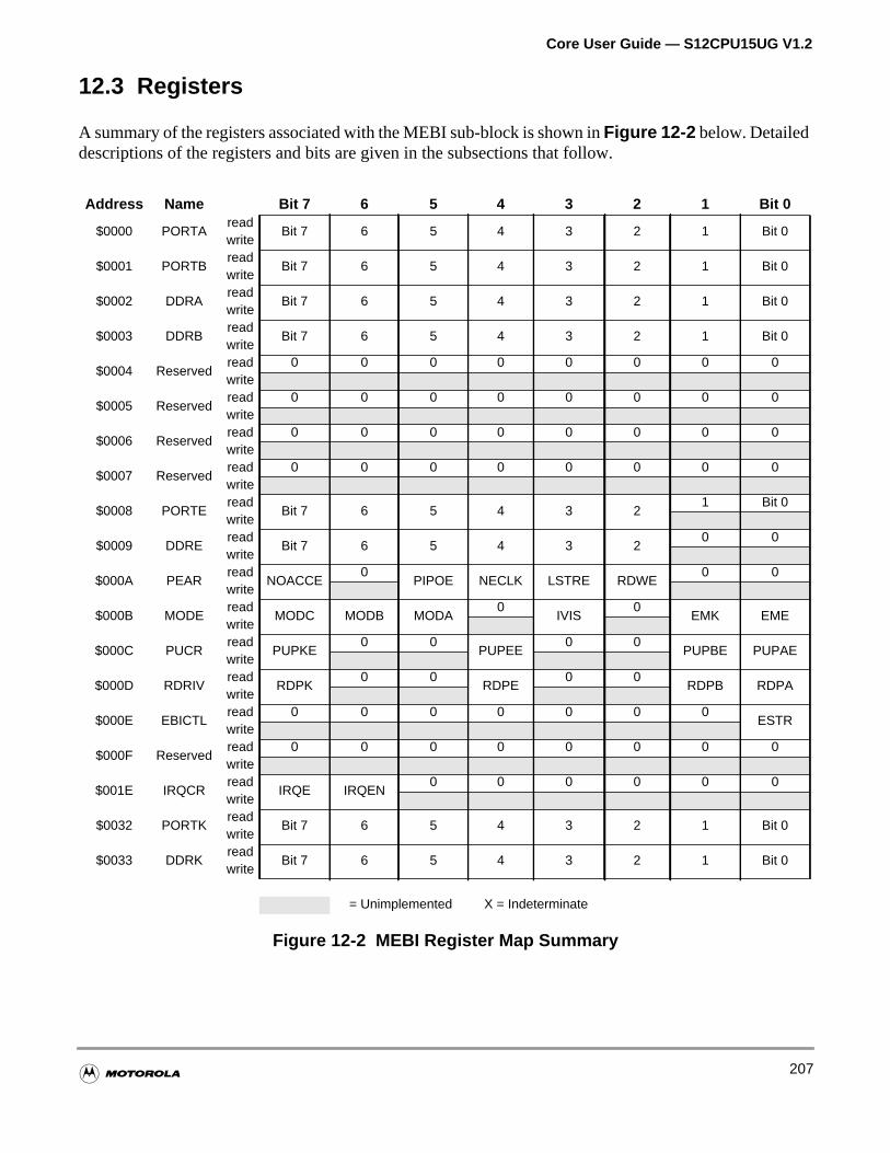
Core User Guide — S12CPU15UG V1.2
12.3 Registers
A summary of the registers associated with the MEBI sub-block is shown inFigure 12-2 below. Detaileddescriptions of the registers and bits are given in the subsections that follow.
Figure 12-2 MEBI Register Map Summary
Address Name Bit 7 6 5 4 3 2 1 Bit 0
$0000 PORTAread
Bit 7 6 5 4 3 2 1 Bit 0write
$0001 PORTBread
Bit 7 6 5 4 3 2 1 Bit 0write
$0002 DDRAread
Bit 7 6 5 4 3 2 1 Bit 0write
$0003 DDRBread
Bit 7 6 5 4 3 2 1 Bit 0write
$0004 Reservedread 0 0 0 0 0 0 0 0write
$0005 Reservedread 0 0 0 0 0 0 0 0write
$0006 Reservedread 0 0 0 0 0 0 0 0write
$0007 Reservedread 0 0 0 0 0 0 0 0write
$0008 PORTEread
Bit 7 6 5 4 3 21 Bit 0
write
$0009 DDREread
Bit 7 6 5 4 3 20 0
write
$000A PEARread
NOACCE0
PIPOE NECLK LSTRE RDWE0 0
write
$000B MODEread
MODC MODB MODA0
IVIS0
EMK EMEwrite
$000C PUCRread
PUPKE0 0
PUPEE0 0
PUPBE PUPAEwrite
$000D RDRIVread
RDPK0 0
RDPE0 0
RDPB RDPAwrite
$000E EBICTLread 0 0 0 0 0 0 0
ESTRwrite
$000F Reservedread 0 0 0 0 0 0 0 0write
$001E IRQCRread
IRQE IRQEN0 0 0 0 0 0
write
$0032 PORTKread
Bit 7 6 5 4 3 2 1 Bit 0write
$0033 DDRKread
Bit 7 6 5 4 3 2 1 Bit 0write
= Unimplemented X = Indeterminate
207
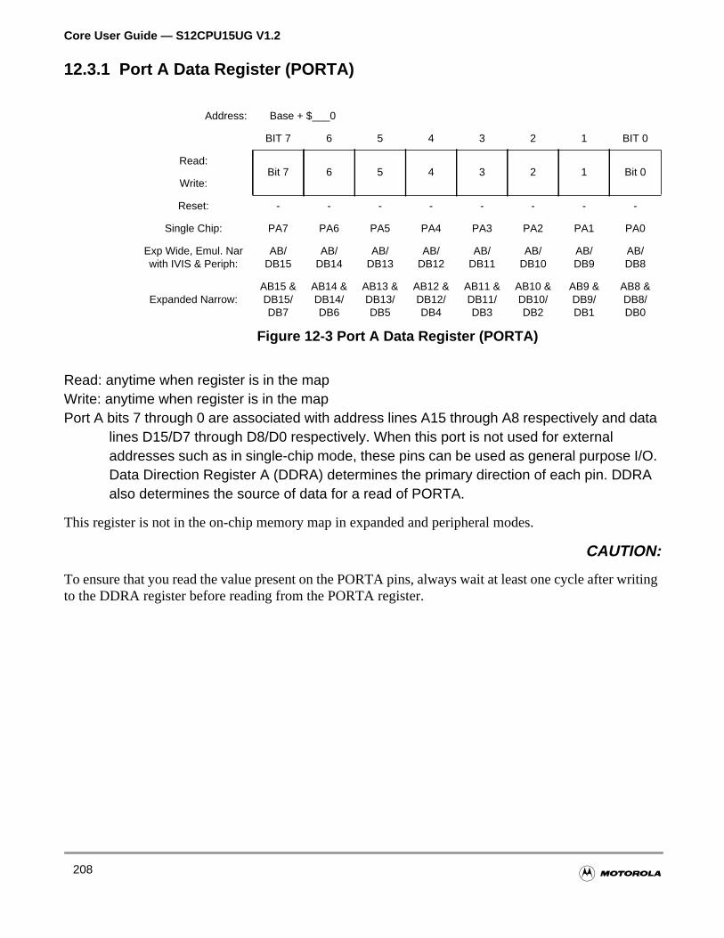
Core User Guide — S12CPU15UG V1.2
riting
12.3.1 Port A Data Register (PORTA)
Read: anytime when register is in the mapWrite: anytime when register is in the mapPort A bits 7 through 0 are associated with address lines A15 through A8 respectively and data
lines D15/D7 through D8/D0 respectively. When this port is not used for externaladdresses such as in single-chip mode, these pins can be used as general purpose I/O.Data Direction Register A (DDRA) determines the primary direction of each pin. DDRAalso determines the source of data for a read of PORTA.
This register is not in the on-chip memory map in expanded and peripheral modes.
CAUTION:
To ensure that you read the value present on the PORTA pins, always wait at least one cycle after wto the DDRA register before reading from the PORTA register.
Address: Base + $___0
BIT 7 6 5 4 3 2 1 BIT 0
Read:Bit 7 6 5 4 3 2 1 Bit 0
Write:
Reset: - - - - - - - -
Single Chip: PA7 PA6 PA5 PA4 PA3 PA2 PA1 PA0
Exp Wide, Emul. Narwith IVIS & Periph:
AB/DB15
AB/DB14
AB/DB13
AB/DB12
AB/DB11
AB/DB10
AB/DB9
AB/DB8
Expanded Narrow:AB15 &DB15/DB7
AB14 &DB14/DB6
AB13 &DB13/DB5
AB12 &DB12/DB4
AB11 &DB11/DB3
AB10 &DB10/DB2
AB9 &DB9/DB1
AB8 &DB8/DB0
Figure 12-3 Port A Data Register (PORTA)
208
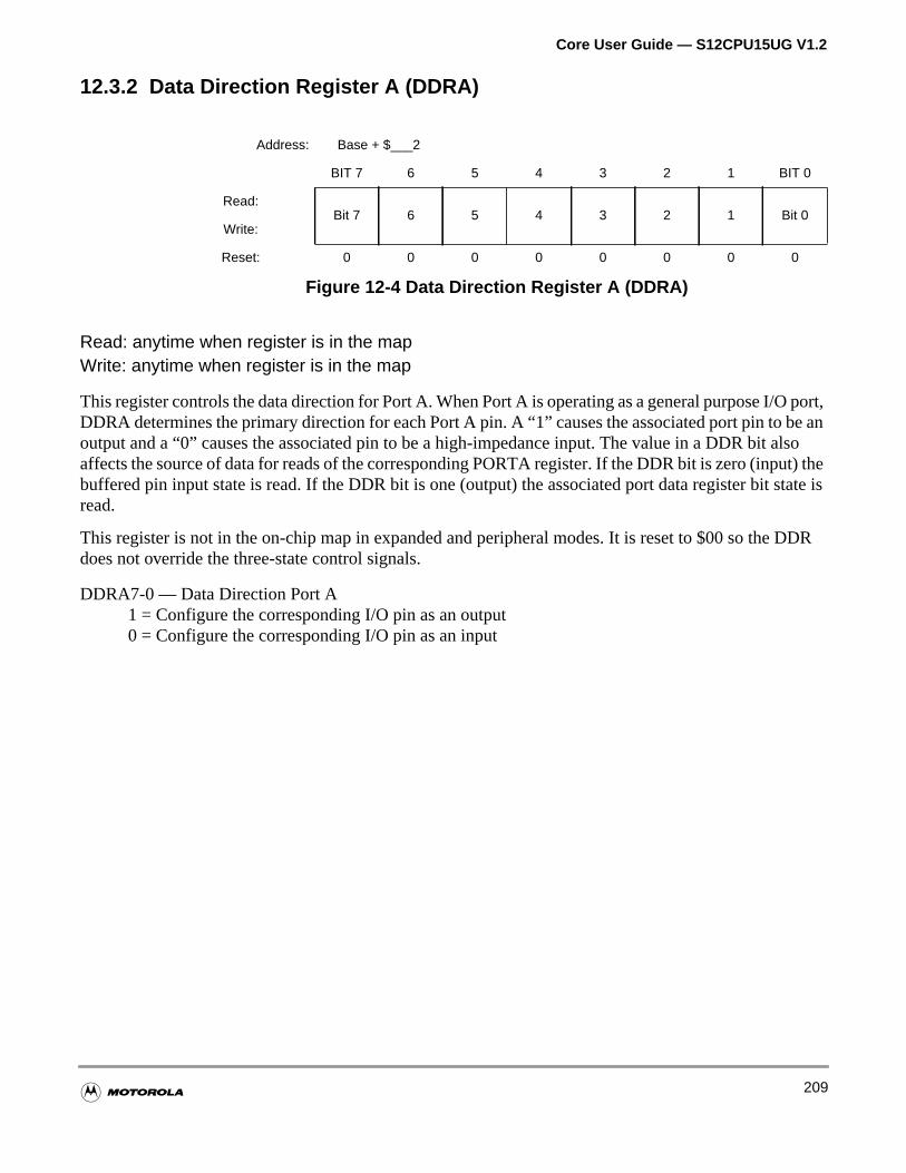
Core User Guide — S12CPU15UG V1.2
port,e an
alsot) thestate is
DDR
12.3.2 Data Direction Register A (DDRA)
Read: anytime when register is in the mapWrite: anytime when register is in the map
This register controls the data direction for Port A. When Port A is operating as a general purpose I/ODDRA determines the primary direction for each Port A pin. A “1” causes the associated port pin to boutput and a “0” causes the associated pin to be a high-impedance input. The value in a DDR bit affects the source of data for reads of the corresponding PORTA register. If the DDR bit is zero (inpubuffered pin input state is read. If the DDR bit is one (output) the associated port data register bit read.
This register is not in the on-chip map in expanded and peripheral modes. It is reset to $00 so thedoes not override the three-state control signals.
DDRA7-0 — Data Direction Port A1 = Configure the corresponding I/O pin as an output0 = Configure the corresponding I/O pin as an input
Address: Base + $___2
BIT 7 6 5 4 3 2 1 BIT 0
Read:Bit 7 6 5 4 3 2 1 Bit 0
Write:
Reset: 0 0 0 0 0 0 0 0
Figure 12-4 Data Direction Register A (DDRA)
209
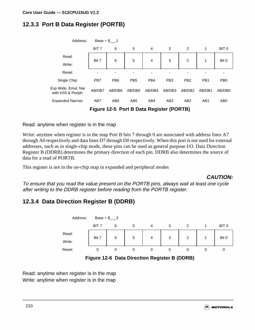
Core User Guide — S12CPU15UG V1.2
es A7ternalectionce of
12.3.3 Port B Data Register (PORTB)
Read: anytime when register is in the map
Write: anytime when register is in the map Port B bits 7 through 0 are associated with address linthrough A0 respectively and data lines D7 through D0 respectively. When this port is not used for exaddresses, such as in single-chip mode, these pins can be used as general purpose I/O. Data DirRegister B (DDRB) determines the primary direction of each pin. DDRB also determines the sourdata for a read of PORTB.
This register is not in the on-chip map in expanded and peripheral modes
CAUTION:To ensure that you read the value present on the PORTB pins, always wait at least one cycleafter writing to the DDRB register before reading from the PORTB register.
12.3.4 Data Direction Register B (DDRB)
Read: anytime when register is in the mapWrite: anytime when register is in the map
Address: Base + $___1
BIT 7 6 5 4 3 2 1 BIT 0
Read:Bit 7 6 5 4 3 2 1 Bit 0
Write:
Reset: - - - - - - - -
Single Chip: PB7 PB6 PB5 PB4 PB3 PB2 PB1 PB0
Exp Wide, Emul. Narwith IVIS & Periph:
AB/DB7 AB/DB6 AB/DB5 AB/DB4 AB/DB3 AB/DB2 AB/DB1 AB/DB0
Expanded Narrow: AB7 AB6 AB5 AB4 AB3 AB2 AB1 AB0
Figure 12-5 Port B Data Register (PORTB)
Address: Base + $___3
BIT 7 6 5 4 3 2 1 BIT 0
Read:Bit 7 6 5 4 3 2 1 Bit 0
Write:
Reset: 0 0 0 0 0 0 0 0
Figure 12-6 Data Direction Register B (DDRB)
210
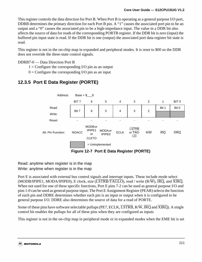
Core User Guide — S12CPU15UG V1.2
port,be analsot) the
state is
DDR
lect
I/O andunctionbe
it is set
This register controls the data direction for Port B. When Port B is operating as a general purpose I/ODDRB determines the primary direction for each Port B pin. A “1” causes the associated port pin tooutput and a “0” causes the associated pin to be a high-impedance input. The value in a DDR bit affects the source of data for reads of the corresponding PORTB register. If the DDR bit is zero (inpubuffered pin input state is read. If the DDR bit is one (output) the associated port data register bit read.
This register is not in the on-chip map in expanded and peripheral modes. It is reset to $00 so thedoes not override the three-state control signals.
DDRB7-0 — Data Direction Port B1 = Configure the corresponding I/O pin as an output0 = Configure the corresponding I/O pin as an input
12.3.5 Port E Data Register (PORTE)
Read: anytime when register is in the mapWrite: anytime when register is in the map
Port E is associated with external bus control signals and interrupt inputs. These include mode se(MODB/IPIPE1, MODA/IPIPE0), E clock, size (LSTRB/TAGLO), read / write (R/W), IRQ, andXIRQ.When not used for one of these specific functions, Port E pins 7-2 can be used as general purposepins 1-0 can be used as general purpose input. The Port E Assignment Register (PEAR) selects the fof each pin and DDRE determines whether each pin is an input or output when it is configured to general purpose I/O. DDRE also determines the source of data for a read of PORTE.
Some of these pins have software selectable pullups (PE7, ECLK,LSTRB, R/W, IRQ andXIRQ). A singlecontrol bit enables the pullups for all of these pins when they are configured as inputs
This register is not in the on-chip map in peripheral mode or in expanded modes when the EME b
Address: Base + $___8
BIT 7 6 5 4 3 2 1 BIT 0
Read:Bit 7 6 5 4 3 2
Bit 1 Bit 0
Write:
Reset: - - - - - - - -
Alt. Pin Function: NOACC
MODBorIPIPE1
orCLKTO
MODAorIPIPE0
ECLKLSTRBor TAG-
LOR/W IRQ XIRQ
= Unimplemented
Figure 12-7 Port E Data Register (PORTE)
211
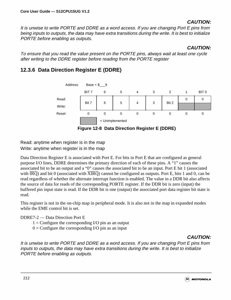
Core User Guide — S12CPU15UG V1.2
ral
ociatedbeffectsestate is
odes
CAUTION:It is unwise to write PORTE and DDRE as a word access. If you are changing Port E pins frombeing inputs to outputs, the data may have extra transitions during the write. It is best to initializePORTE before enabling as outputs.
CAUTION:To ensure that you read the value present on the PORTE pins, always wait at least one cycleafter writing to the DDRE register before reading from the PORTE register
12.3.6 Data Direction Register E (DDRE)
Read: anytime when register is in the mapWrite: anytime when register is in the map
Data Direction Register E is associated with Port E. For bits in Port E that are configured as genepurpose I/O lines, DDRE determines the primary direction of each of these pins. A “1” causes theassociated bit to be an output and a “0” causes the associated bit to be an input. Port E bit 1 (asswith IRQ) and bit 0 (associated withXIRQ) cannot be configured as outputs. Port E, bits 1 and 0, canread regardless of whether the alternate interrupt function is enabled. The value in a DDR bit also athe source of data for reads of the corresponding PORTE register. If the DDR bit is zero (input) thbuffered pin input state is read. If the DDR bit is one (output) the associated port data register bit read.
This register is not in the on-chip map in peripheral mode. It is also not in the map in expanded mwhile the EME control bit is set.
DDRE7-2 — Data Direction Port E1 = Configure the corresponding I/O pin as an output0 = Configure the corresponding I/O pin as an input
CAUTION:It is unwise to write PORTE and DDRE as a word access. If you are changing Port E pins frominputs to outputs, the data may have extra transitions during the write. It is best to initializePORTE before enabling as outputs.
Address: Base + $___9
BIT 7 6 5 4 3 2 1 BIT 0
Read:Bit 7 6 5 4 3 Bit 2
0 0
Write:
Reset: 0 0 0 0 0 0 0 0
= Unimplemented
Figure 12-8 Data Direction Register E (DDRE)
212
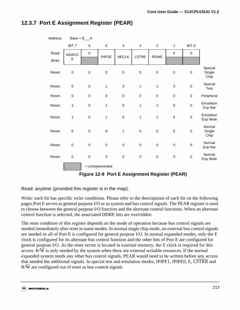
Core User Guide — S12CPU15UG V1.2
owingr is usedternate
aresignalsy the E for thisl access
12.3.7 Port E Assignment Register (PEAR)
Read: anytime (provided this register is in the map).
Write: each bit has specific write conditions. Please refer to the descriptions of each bit on the follpages.Port E serves as general purpose I/O or as system and bus control signals. The PEAR registeto choose between the general purpose I/O function and the alternate control functions. When an alcontrol function is selected, the associated DDRE bits are overridden.
The reset condition of this register depends on the mode of operation because bus control signalsneeded immediately after reset in some modes. In normal single chip mode, no external bus controlare needed so all of Port E is configured for general purpose I/O. In normal expanded modes, onlclock is configured for its alternate bus control function and the other bits of Port E are configuredgeneral purpose I/O. As the reset vector is located in external memory, the E clock is required foraccess. R/W is only needed by the system when there are external writable resources. If the normaexpanded system needs any other bus control signals, PEAR would need to be written before anythat needed the additional signals. In special test and emulation modes, IPIPE1, IPIPE0, E,LSTRB andR/W are configured out of reset as bus control signals
Address: Base + $___A
BIT 7 6 5 4 3 2 1 BIT 0
Read: NOACCE
0PIPOE NECLK LSTRE RDWE
0 0
Write:
Reset: 0 0 0 0 0 0 0 0SpecialSingleChip
Reset: 0 0 1 0 1 1 0 0Special
Test
Reset: 0 0 0 0 0 0 0 0 Peripheral
Reset: 1 0 1 0 1 1 0 0EmulationExp Nar
Reset: 1 0 1 0 1 1 0 0EmulationExp Wide
Reset: 0 0 0 1 0 0 0 0NormalSingleChip
Reset: 0 0 0 0 0 0 0 0NormalExp Nar
Reset: 0 0 0 0 0 0 0 0Normal
Exp Wide
= Unimplemented
Figure 12-9 Port E Assignment Register (PEAR)
213
Core User Guide — S12CPU15UG V1.2
cycle.
queue
ng if
This register is not in the on-chip map in emulation and peripheral modes.
NOACCE - CPU No Access Output Enable
Normal: write once
Emulation: write never
Special: write anytime1 = The associated pin (Port E bit 7) is output and indicates whether the cycle is a CPU free0 = The associated pin (Port E bit 7) is general purpose I/O.
This bit has no effect in single chip or peripheral modes.
PIPOE - Pipe Status Signal Output Enable
Normal: write once
Emulation: write never
Special: write anytime.1 = The associated pins (Port E bits 6:5) are outputs and indicate the state of the instruction0 = The associated pins (Port E bits 6:5) are general purpose I/O.
This bit has no effect in single chip or peripheral modes.
NECLK - No External E Clock
Normal and Special: write anytime
Emulation: write never1 = The associated pin (Port E bit-4) is a general purpose I/O pin.0 = The associated pin (Port E bit-4) is the external E clock pin. External E clock is free-runni
ESTR=0
External E clock is available as an output in all modes.
LSTRE - Low Strobe (LSTRB) Enable
Normal: write once
Emulation: write never
Special: write anytime.1 = The associated pin (Port E bit-3) is configured as theLSTRB bus control output. If BDM
tagging is enabled,TAGLO is multiplexed in on the rising edge of ECLK andLSTRB is drivenout on the falling edge of ECLK.
0 = The associated pin (Port E bit-3) is a general purpose I/O pin.
This bit has no effect in single chip, peripheral or normal expanded narrow modes.
NOTE: LSTRB is used during external writes. After reset in normal expanded mode,LSTRBis disabled to provide an extra I/O pin. IfLSTRB is needed, it should be enabledbefore any external writes. External reads do not normally needLSTRB because all16 data bits can be driven even if the system only needs 8 bits of data.
RDWE - Read / Write Enable
Normal: write once
214
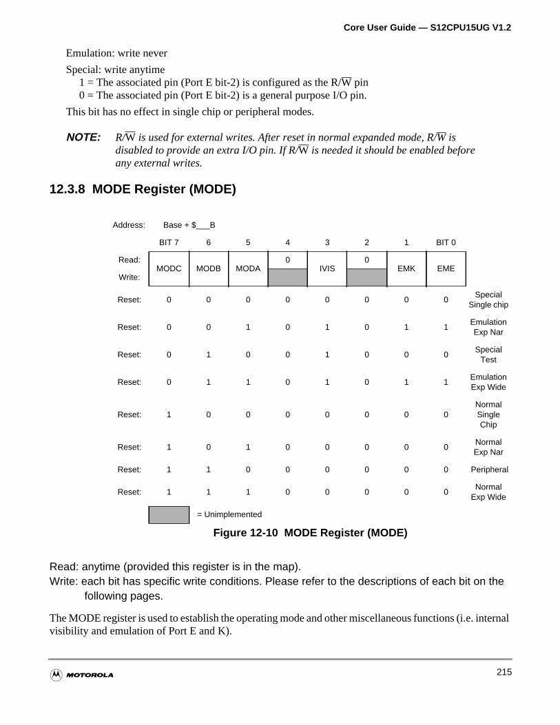
Core User Guide — S12CPU15UG V1.2
nternal
Emulation: write never
Special: write anytime1 = The associated pin (Port E bit-2) is configured as the R/W pin0 = The associated pin (Port E bit-2) is a general purpose I/O pin.
This bit has no effect in single chip or peripheral modes.
NOTE: R/W is used for external writes. After reset in normal expanded mode, R/W isdisabled to provide an extra I/O pin. If R/W is needed it should be enabled beforeany external writes.
12.3.8 MODE Register (MODE)
Read: anytime (provided this register is in the map).Write: each bit has specific write conditions. Please refer to the descriptions of each bit on the
following pages.
The MODE register is used to establish the operating mode and other miscellaneous functions (i.e. ivisibility and emulation of Port E and K).
Address: Base + $___B
BIT 7 6 5 4 3 2 1 BIT 0
Read:MODC MODB MODA
0IVIS
0EMK EME
Write:
Reset: 0 0 0 0 0 0 0 0Special
Single chip
Reset: 0 0 1 0 1 0 1 1EmulationExp Nar
Reset: 0 1 0 0 1 0 0 0Special
Test
Reset: 0 1 1 0 1 0 1 1EmulationExp Wide
Reset: 1 0 0 0 0 0 0 0NormalSingleChip
Reset: 1 0 1 0 0 0 0 0NormalExp Nar
Reset: 1 1 0 0 0 0 0 0 Peripheral
Reset: 1 1 1 0 0 0 0 0Normal
Exp Wide
= Unimplemented
Figure 12-10 MODE Register (MODE)
215
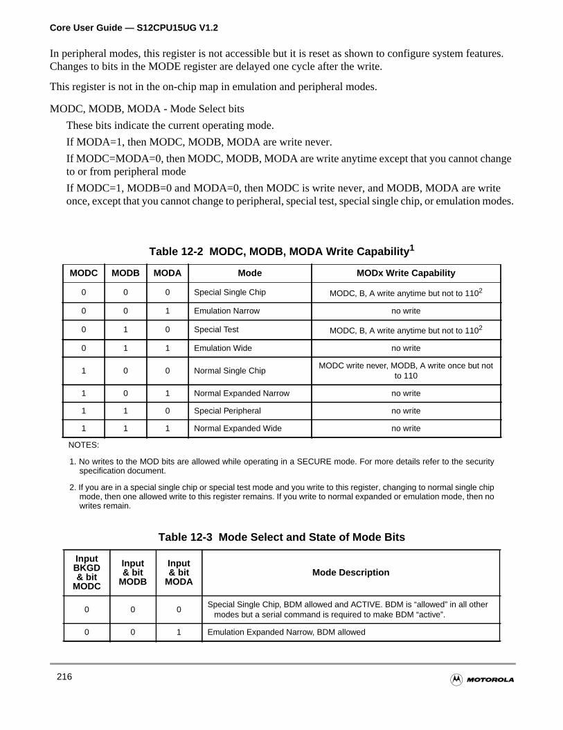
Core User Guide — S12CPU15UG V1.2
tures.
ge
modes.
In peripheral modes, this register is not accessible but it is reset as shown to configure system feaChanges to bits in the MODE register are delayed one cycle after the write.
This register is not in the on-chip map in emulation and peripheral modes.
MODC, MODB, MODA - Mode Select bits
These bits indicate the current operating mode.
If MODA=1, then MODC, MODB, MODA are write never.
If MODC=MODA=0, then MODC, MODB, MODA are write anytime except that you cannot chanto or from peripheral mode
If MODC=1, MODB=0 and MODA=0, then MODC is write never, and MODB, MODA are writeonce, except that you cannot change to peripheral, special test, special single chip, or emulation
Table 12-2 MODC, MODB, MODA Write Capability 1
NOTES:
1. No writes to the MOD bits are allowed while operating in a SECURE mode. For more details refer to the securityspecification document.
MODC MODB MODA Mode MODx Write Capability
0 0 0 Special Single Chip MODC, B, A write anytime but not to 1102
2. If you are in a special single chip or special test mode and you write to this register, changing to normal single chipmode, then one allowed write to this register remains. If you write to normal expanded or emulation mode, then nowrites remain.
0 0 1 Emulation Narrow no write
0 1 0 Special Test MODC, B, A write anytime but not to 1102
0 1 1 Emulation Wide no write
1 0 0 Normal Single ChipMODC write never, MODB, A write once but not
to 110
1 0 1 Normal Expanded Narrow no write
1 1 0 Special Peripheral no write
1 1 1 Normal Expanded Wide no write
Table 12-3 Mode Select and State of Mode Bits
InputBKGD& bit
MODC
Input& bit
MODB
Input& bit
MODAMode Description
0 0 0Special Single Chip, BDM allowed and ACTIVE. BDM is “allowed” in all other
modes but a serial command is required to make BDM “active”.
0 0 1 Emulation Expanded Narrow, BDM allowed
216
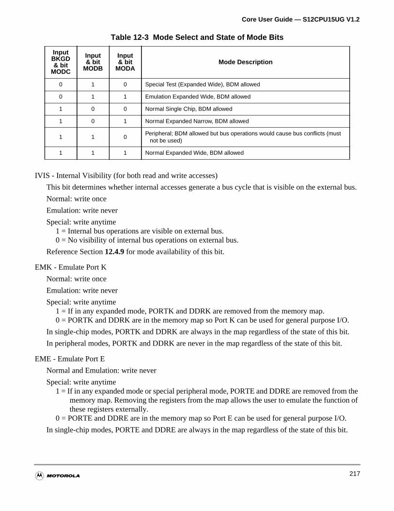
Core User Guide — S12CPU15UG V1.2
nal bus.
I/O.
bit.
it.
m theon of
I/O.
bit.
IVIS - Internal Visibility (for both read and write accesses)
This bit determines whether internal accesses generate a bus cycle that is visible on the exter
Normal: write once
Emulation: write never
Special: write anytime1 = Internal bus operations are visible on external bus.0 = No visibility of internal bus operations on external bus.
Reference Section12.4.9 for mode availability of this bit.
EMK - Emulate Port K
Normal: write once
Emulation: write never
Special: write anytime1 = If in any expanded mode, PORTK and DDRK are removed from the memory map.0 = PORTK and DDRK are in the memory map so Port K can be used for general purpose
In single-chip modes, PORTK and DDRK are always in the map regardless of the state of this
In peripheral modes, PORTK and DDRK are never in the map regardless of the state of this b
EME - Emulate Port E
Normal and Emulation: write never
Special: write anytime1 = If in any expanded mode or special peripheral mode, PORTE and DDRE are removed fro
memory map. Removing the registers from the map allows the user to emulate the functithese registers externally.
0 = PORTE and DDRE are in the memory map so Port E can be used for general purpose
In single-chip modes, PORTE and DDRE are always in the map regardless of the state of this
0 1 0 Special Test (Expanded Wide), BDM allowed
0 1 1 Emulation Expanded Wide, BDM allowed
1 0 0 Normal Single Chip, BDM allowed
1 0 1 Normal Expanded Narrow, BDM allowed
1 1 0Peripheral; BDM allowed but bus operations would cause bus conflicts (must
not be used)
1 1 1 Normal Expanded Wide, BDM allowed
Table 12-3 Mode Select and State of Mode Bits
InputBKGD& bit
MODC
Input& bit
MODB
Input& bit
MODAMode Description
217
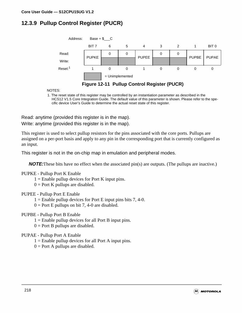
Core User Guide — S12CPU15UG V1.2
arered as
tive.)
12.3.9 Pullup Control Register (PUCR)
Read: anytime (provided this register is in the map).Write: anytime (provided this register is in the map).
This register is used to select pullup resistors for the pins associated with the core ports. Pullups assigned on a per-port basis and apply to any pin in the corresponding port that is currently configuan input.
This register is not in the on-chip map in emulation and peripheral modes.
NOTE:These bits have no effect when the associated pin(s) are outputs. (The pullups are inac
PUPKE - Pullup Port K Enable1 = Enable pullup devices for Port K input pins.0 = Port K pullups are disabled.
PUPEE - Pullup Port E Enable1 = Enable pullup devices for Port E input pins bits 7, 4-0.0 = Port E pullups on bit 7, 4-0 are disabled.
PUPBE - Pullup Port B Enable1 = Enable pullup devices for all Port B input pins.0 = Port B pullups are disabled.
PUPAE - Pullup Port A Enable1 = Enable pullup devices for all Port A input pins.0 = Port A pullups are disabled.
Address: Base + $___C
BIT 7 6 5 4 3 2 1 BIT 0
Read:PUPKE
0 0PUPEE
0 0PUPBE PUPAE
Write:
Reset:1
NOTES:1. The reset state of this register may be controlled by an instantiation parameter as described in the
HCS12 V1.5 Core Integration Guide. The default value of this parameter is shown. Please refer to the spe-cific device User’s Guide to determine the actual reset state of this register.
1 0 0 1 0 0 0 0
= Unimplemented
Figure 12-11 Pullup Control Register (PUCR)
218
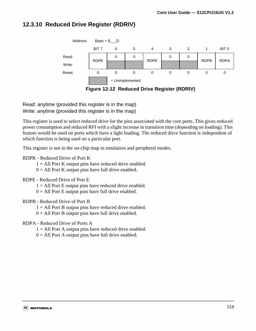
Core User Guide — S12CPU15UG V1.2
duced. Thisent of
12.3.10 Reduced Drive Register (RDRIV)
Read: anytime (provided this register is in the map)Write: anytime (provided this register is in the map)
This register is used to select reduced drive for the pins associated with the core ports. This gives repower consumption and reduced RFI with a slight increase in transition time (depending on loading)feature would be used on ports which have a light loading. The reduced drive function is independwhich function is being used on a particular port.
This register is not in the on-chip map in emulation and peripheral modes.
RDPK - Reduced Drive of Port K1 = All Port K output pins have reduced drive enabled.0 = All Port K output pins have full drive enabled.
RDPE - Reduced Drive of Port E1 = All Port E output pins have reduced drive enabled.0 = All Port E output pins have full drive enabled.
RDPB - Reduced Drive of Port B1 = All Port B output pins have reduced drive enabled.0 = All Port B output pins have full drive enabled.
RDPA - Reduced Drive of Ports A1 = All Port A output pins have reduced drive enabled.0 = All Port A output pins have full drive enabled.
Address: Base + $___D
BIT 7 6 5 4 3 2 1 BIT 0
Read:RDPK
0 0RDPE
0 0RDPB RDPA
Write:
Reset: 0 0 0 0 0 0 0 0
= Unimplemented
Figure 12-12 Reduced Drive Register (RDRIV)
219
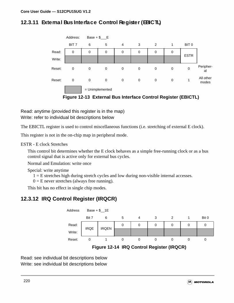
Core User Guide — S12CPU15UG V1.2
).
bus
12.3.11 External Bus Interface Control Register (EBICTL)
Read: anytime (provided this register is in the map)Write: refer to individual bit descriptions below
The EBICTL register is used to control miscellaneous functions (i.e. stretching of external E clock
This register is not in the on-chip map in peripheral mode.
ESTR - E clock Stretches
This control bit determines whether the E clock behaves as a simple free-running clock or as acontrol signal that is active only for external bus cycles.
Normal and Emulation: write once
Special: write anytime1 = E stretches high during stretch cycles and low during non-visible internal accesses.0 = E never stretches (always free running).
This bit has no effect in single chip modes.
12.3.12 IRQ Control Register (IRQCR)
Read: see individual bit descriptions belowWrite: see individual bit descriptions below
Address: Base + $___E
BIT 7 6 5 4 3 2 1 BIT 0
Read: 0 0 0 0 0 0 0ESTR
Write:
Reset: 0 0 0 0 0 0 0 0Peripher-
al
Reset: 0 0 0 0 0 0 0 1All othermodes
= Unimplemented
Figure 12-13 External Bus Interface Control Register (EBICTL)
Address Base + $__1E
Bit 7 6 5 4 3 2 1 Bit 0
Read:IRQE IRQEN
0 0 0 0 0 0
Write:
Reset: 0 1 0 0 0 0 0 0
Figure 12-14 IRQ Control Register (IRQCR)
220
Core User Guide — S12CPU15UG V1.2
ctedrupt
IRQE - IRQ select edge sensitive only
Special: read or write anytime
Normal: read anytime, write once
Emulation: read anytime, write never1 = IRQ configured to respond only to falling edges. Falling edges on the IRQ pin will be dete
anytime IRQE = 1 and will be cleared only upon a reset or the servicing of the IRQ inter(i.e. vector = $FFF2).
0 = IRQ configured for low level recognition
IRQEN - External IRQ enable
Normal, emulation, and special modes: read or write anytime1 = External IRQ pin is connected to interrupt logic.0 = External IRQ pin is disconnected from interrupt logic
NOTE: In this state the edge detect latch is disabled.
221

Core User Guide — S12CPU15UG V1.2
abledort K isin. A
its infect.
12.3.13 Reserved Registers .
12.3.14 Port K Data Register (PORTK) .
Read: anytimeWrite: anytime
This port is associated with the internal memory expansion emulation pins. When the port is not ento emulate the internal memory expansion, the port pins are used as general-purpose I/O. When Poperating as a general purpose I/O port, DDRK determines the primary direction for each Port K p“1” causes the associated port pin to be an output and a “0” causes the associated pin to be a
Address: Base + $___4 thru $___7
BIT 7 6 5 4 3 2 1 BIT 0
Read: 0 0 0 0 0 0 0 0
Write:
Reset: 0 0 0 0 0 0 0 0
Address: Base + $___F
Read: 0 0 0 0 0 0 0 0
Write:
Reset: 0 0 0 0 0 0 0 0
= Unimplemented
Figure 12-15 Reserved Registers
These register locations are not used (reserved). All unused registers and bthis block return logic zeros when read. Writes to these registers have no ef
These registers are not in the on-chip map in peripheral mode.
Address: Base + $32
Bit 7 6 5 4 3 2 1 Bit 0
Read:Bit 7 6 5 4 3 2 1 Bit 0
Write:
Alt. pinfunction
ECS XCS XAB19 XAB18 XAB17 XAB16 XAB15 XAB14
Reset: - - - - - - - -
= Unimplemented
Figure 12-16 Port K Data Register (PORTK)
222
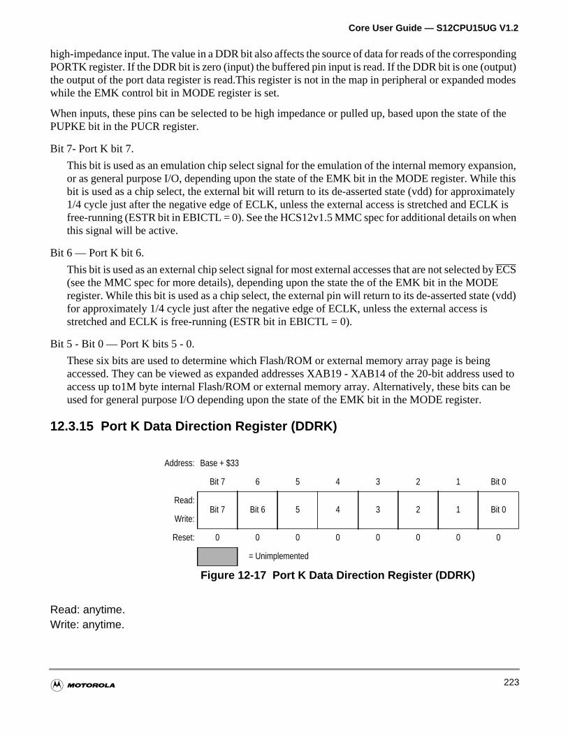
Core User Guide — S12CPU15UG V1.2
ndingut)
modes
of the
sion,this
matelyLK ishen
byE(vdd)
g used ton be
high-impedance input. The value in a DDR bit also affects the source of data for reads of the correspoPORTK register. If the DDR bit is zero (input) the buffered pin input is read. If the DDR bit is one (outpthe output of the port data register is read.This register is not in the map in peripheral or expandedwhile the EMK control bit in MODE register is set.
When inputs, these pins can be selected to be high impedance or pulled up, based upon the statePUPKE bit in the PUCR register.
Bit 7- Port K bit 7.
This bit is used as an emulation chip select signal for the emulation of the internal memory expanor as general purpose I/O, depending upon the state of the EMK bit in the MODE register. Whilebit is used as a chip select, the external bit will return to its de-asserted state (vdd) for approxi1/4 cycle just after the negative edge of ECLK, unless the external access is stretched and ECfree-running (ESTR bit in EBICTL = 0). See the HCS12v1.5 MMC spec for additional details on wthis signal will be active.
Bit 6 — Port K bit 6.
This bit is used as an external chip select signal for most external accesses that are not selectedECS(see the MMC spec for more details), depending upon the state the of the EMK bit in the MODregister. While this bit is used as a chip select, the external pin will return to its de-asserted statefor approximately 1/4 cycle just after the negative edge of ECLK, unless the external access isstretched and ECLK is free-running (ESTR bit in EBICTL = 0).
Bit 5 - Bit 0 — Port K bits 5 - 0.
These six bits are used to determine which Flash/ROM or external memory array page is beinaccessed. They can be viewed as expanded addresses XAB19 - XAB14 of the 20-bit addressaccess up to1M byte internal Flash/ROM or external memory array. Alternatively, these bits caused for general purpose I/O depending upon the state of the EMK bit in the MODE register.
12.3.15 Port K Data Direction Register (DDRK)
Read: anytime.Write: anytime.
Address: Base + $33
Bit 7 6 5 4 3 2 1 Bit 0
Read:Bit 7 Bit 6 5 4 3 2 1 Bit 0
Write:
Reset: 0 0 0 0 0 0 0 0
= Unimplemented
Figure 12-17 Port K Data Direction Register (DDRK)
223
Core User Guide — S12CPU15UG V1.2
. Thisister
ntrol
nternalus to6-biting each
ignals.
d with
This register determines the primary direction for each port K pin configured as general-purpose I/Oregister is not in the map in peripheral or expanded modes while the EMK control bit in MODE regis set.
DDRK 7-0 - The Data Direction Port K.1 = Associated pin is an output0 = Associated pin is a high-impedance input
CAUTION:It is unwise to write PORTK and DDRK as a word access. If you are changing Port K pins frominputs to outputs, the data may have extra transitions during the write. It is best to initializePORTK before enabling as outputs.
CAUTION:To ensure that you read the correct value from the PORTK pins, always wait at least one cycleafter writing to the DDRK register before reading from the PORTK register.
12.4 Operation
There are four main sub-blocks within the MEBI: external bus control, external data bus interface, coand registers.
12.4.1 External Bus Control
The external bus control generates the miscellaneous control functions (pipe signals, ECLK,LSTRB andR/W) that will be sent external on Port E, bits 6-2. It also generates the external addresses.
12.4.2 External Data Bus Interface
The external data bus interface block manages data transfers from/to the external pins to/from the iread and write data buses. This block selectively couples 8-bit or 16-bit data to the internal data bimplement a variety of data transfers including 8-bit, 16-bit, 16-bit swapped and 8-bit external to 1internal accesses. Modes, addresses, chip selects, etc. affect the type of accesses performed durbus cycle.
12.4.3 Control
The control block generates the register read/write control signals and miscellaneous port control s
12.4.4 Registers
The register block includes the fourteen 8-bit registers and five reserved register locations associatethe MEBI sub-block.
224
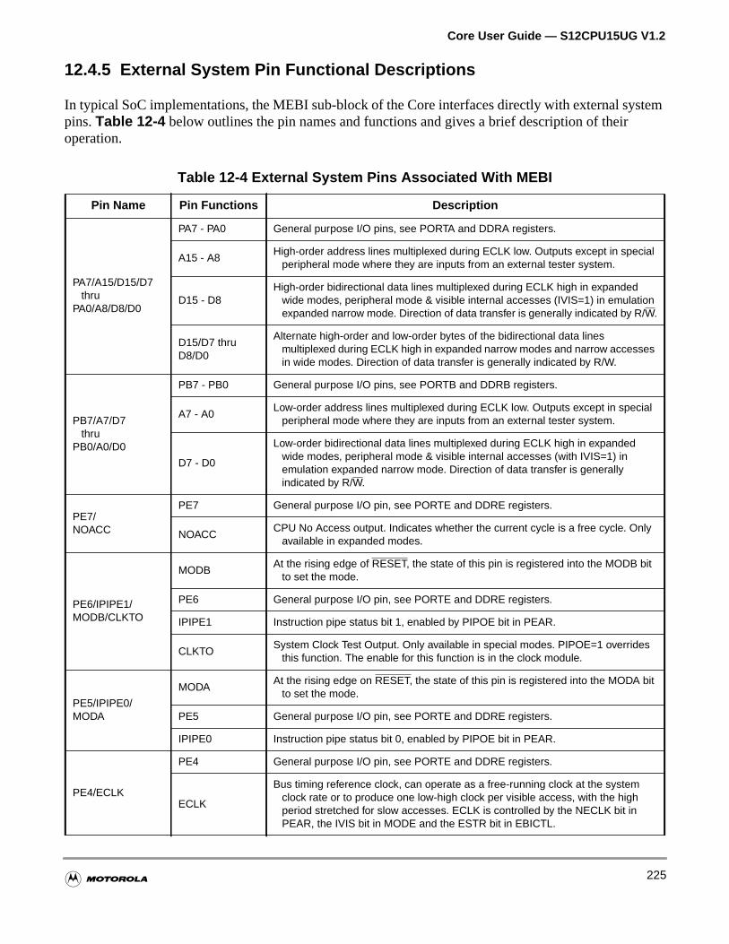
Core User Guide — S12CPU15UG V1.2
tem
12.4.5 External System Pin Functional Descriptions
In typical SoC implementations, the MEBI sub-block of the Core interfaces directly with external syspins.Table 12-4 below outlines the pin names and functions and gives a brief description of theiroperation.
Table 12-4 External System Pins Associated With MEBI
Pin Name Pin Functions Description
PA7/A15/D15/D7thru
PA0/A8/D8/D0
PA7 - PA0 General purpose I/O pins, see PORTA and DDRA registers.
A15 - A8High-order address lines multiplexed during ECLK low. Outputs except in special
peripheral mode where they are inputs from an external tester system.
D15 - D8High-order bidirectional data lines multiplexed during ECLK high in expanded
wide modes, peripheral mode & visible internal accesses (IVIS=1) in emulationexpanded narrow mode. Direction of data transfer is generally indicated by R/W.
D15/D7 thruD8/D0
Alternate high-order and low-order bytes of the bidirectional data linesmultiplexed during ECLK high in expanded narrow modes and narrow accessesin wide modes. Direction of data transfer is generally indicated by R/W.
PB7/A7/D7thru
PB0/A0/D0
PB7 - PB0 General purpose I/O pins, see PORTB and DDRB registers.
A7 - A0Low-order address lines multiplexed during ECLK low. Outputs except in special
peripheral mode where they are inputs from an external tester system.
D7 - D0
Low-order bidirectional data lines multiplexed during ECLK high in expandedwide modes, peripheral mode & visible internal accesses (with IVIS=1) inemulation expanded narrow mode. Direction of data transfer is generallyindicated by R/W.
PE7/NOACC
PE7 General purpose I/O pin, see PORTE and DDRE registers.
NOACCCPU No Access output. Indicates whether the current cycle is a free cycle. Only
available in expanded modes.
PE6/IPIPE1/MODB/CLKTO
MODBAt the rising edge of RESET, the state of this pin is registered into the MODB bit
to set the mode.
PE6 General purpose I/O pin, see PORTE and DDRE registers.
IPIPE1 Instruction pipe status bit 1, enabled by PIPOE bit in PEAR.
CLKTOSystem Clock Test Output. Only available in special modes. PIPOE=1 overrides
this function. The enable for this function is in the clock module.
PE5/IPIPE0/MODA
MODAAt the rising edge on RESET, the state of this pin is registered into the MODA bit
to set the mode.
PE5 General purpose I/O pin, see PORTE and DDRE registers.
IPIPE0 Instruction pipe status bit 0, enabled by PIPOE bit in PEAR.
PE4/ECLK
PE4 General purpose I/O pin, see PORTE and DDRE registers.
ECLK
Bus timing reference clock, can operate as a free-running clock at the systemclock rate or to produce one low-high clock per visible access, with the highperiod stretched for slow accesses. ECLK is controlled by the NECLK bit inPEAR, the IVIS bit in MODE and the ESTR bit in EBICTL.
225
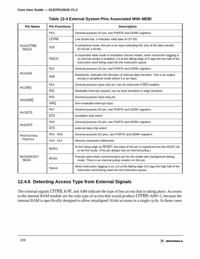
Core User Guide — S12CPU15UG V1.2
ses
cases
12.4.6 Detecting Access Type from External Signals
The external signalsLSTRB, R/W, and AB0 indicate the type of bus access that is taking place. Accesto the internal RAM module are the only type of access that would produceLSTRB=AB0=1, because theinternal RAM is specifically designed to allow misaligned 16-bit accesses in a single cycle. In these
PE3/LSTRB/TAGLO
PE3 General purpose I/O pin, see PORTE and DDRE registers.
LSTRB Low strobe bar, 0 indicates valid data on D7-D0.
SZ8In peripheral mode, this pin is an input indicating the size of the data transfer
(0=16-bit; 1=8-bit).
TAGLOIn expanded wide mode or emulation narrow modes, when instruction tagging is
on and low strobe is enabled, a 0 at the falling edge of E tags the low half of theinstruction word being read into the instruction queue.
PE2/R/W
PE2 General purpose I/O pin, see PORTE and DDRE registers.
R/WRead/write, indicates the direction of internal data transfers. This is an output
except in peripheral mode where it is an input.
PE1/IRQPE1 General purpose input-only pin, can be read even if IRQ enabled.
IRQ Maskable interrupt request, can be level sensitive or edge sensitive.
PE0/XIRQPE0 General purpose input-only pin.
XIRQ Non-maskable interrupt input.
PK7/ECSPK7 General purpose I/O pin, see PORTK and DDRK registers.
ECS emulation chip select
PK6/XCSPK6 General purpose I/O pin, see PORTK and DDRK registers.
XCS external data chip select
PK5/X19 thruPK0/X14
PK5 - PK0 General purpose I/O pins, see PORTK and DDRK registers.
X19 - X14 Memory expansion addresses
BKGD/MODC/TAGHI
MODCAt the rising edge on RESET, the state of this pin is registered into the MODC bit
to set the mode. (This pin always has an internal pullup.)
BKGDPseudo-open-drain communication pin for the single-wire background debug
mode. There is an internal pullup resistor on this pin.
TAGHIWhen instruction tagging is on, a 0 at the falling edge of E tags the high half of the
instruction word being read into the instruction queue.
Table 12-4 External System Pins Associated With MEBI
Pin Name Pin Functions Description
226
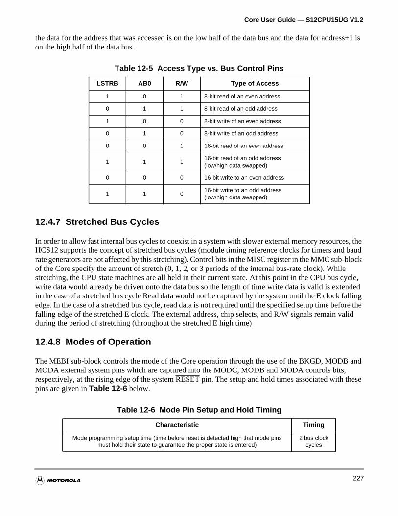
Core User Guide — S12CPU15UG V1.2
ress+1 is
s, thed baudblockecycle,endedfallingfore thevalid
and
se
the data for the address that was accessed is on the low half of the data bus and the data for addon the high half of the data bus.
12.4.7 Stretched Bus Cycles
In order to allow fast internal bus cycles to coexist in a system with slower external memory resourceHCS12 supports the concept of stretched bus cycles (module timing reference clocks for timers anrate generators are not affected by this stretching). Control bits in the MISC register in the MMC sub-of the Core specify the amount of stretch (0, 1, 2, or 3 periods of the internal bus-rate clock). Whilstretching, the CPU state machines are all held in their current state. At this point in the CPU bus write data would already be driven onto the data bus so the length of time write data is valid is extin the case of a stretched bus cycle Read data would not be captured by the system until the E clockedge. In the case of a stretched bus cycle, read data is not required until the specified setup time befalling edge of the stretched E clock. The external address, chip selects, and R/W signals remain during the period of stretching (throughout the stretched E high time)
12.4.8 Modes of Operation
The MEBI sub-block controls the mode of the Core operation through the use of the BKGD, MODBMODA external system pins which are captured into the MODC, MODB and MODA controls bits,respectively, at the rising edge of the systemRESET pin. The setup and hold times associated with thepins are given inTable 12-6 below.
Table 12-5 Access Type vs. Bus Control Pins
LSTRB AB0 R/ W Type of Access
1 0 1 8-bit read of an even address
0 1 1 8-bit read of an odd address
1 0 0 8-bit write of an even address
0 1 0 8-bit write of an odd address
0 0 1 16-bit read of an even address
1 1 116-bit read of an odd address(low/high data swapped)
0 0 0 16-bit write to an even address
1 1 016-bit write to an odd address(low/high data swapped)
Table 12-6 Mode Pin Setup and Hold Timing
Characteristic Timing
Mode programming setup time (time before reset is detected high that mode pinsmust hold their state to guarantee the proper state is entered)
2 bus clockcycles
227

Core User Guide — S12CPU15UG V1.2
e I/Oss and
de andalso
nning,ration.
et sot or
t isthefetchedPE0
n be
systeme activelalntrol
tionalng toreset.ce
IPE1,trol
mode
thet speed
The four 8-bit Ports (A, B, E and K) associated with the MEBI sub-block can serve as general purpospins or alternatively as the address, data and control signals for a multiplexed expansion bus. Addredata are multiplexed on Ports A and B. The control pin functions are dependent on the operating mothe control registers PEAR and MODE. The initial state of bits in the PEAR and MODE registers areestablished during reset to configure various aspects of the expansion bus. After the system is ruapplication software can access the PEAR and MODE registers to modify the expansion bus configu
Some aspects of Port E are not mode dependent. Bit 1 of Port E is a general purpose input or theIRQinterrupt input.IRQ can be enabled by bits in the CPU condition code register but it is inhibited at resthis pin is initially configured as a simple input with a pullup. Bit-0 of Port E is a general purpose inputheXIRQ interrupt input.XIRQ also can be enabled by bits in the CPU condition code register but iinhibited at reset so this pin is initially configured as a simple input with a pullup. The ESTR bit in EBICTL register is set to one by reset in any user mode. This assures that the reset vector can beeven if it is located in an external slow memory device. The PE6/MODB/IPIPE1 and PE5/MODA/IPIpins act as high-impedance mode select inputs during reset.
The following subsections discuss the default bus setup and describe which aspects of the bus cachanged after reset on a per mode basis.
12.4.8.1 Special Single Chip Mode
When the system is reset in this mode, the background debug mode is enabled and “active”. Thedoes not fetch the reset vector and execute application code as it would in other modes. Instead, thbackground mode is in control of CPU execution and BDM firmware is waiting for additional seriacommands through the BKGD pin. When a serial command instructs the system to return to normexecution, the system will be configured as described below unless the reset states of internal coregisters have been changed through background commands after the system was reset.
There is no external expansion bus after reset in this mode. Ports A and B are initially simple bidirecI/O pins that are configured as high-impedance inputs with internal pullups enabled; however, writithe mode select bits in the MODE register (which is allowed in special modes) can change this afterAll of the Port E pins (except PE4/ECLK) are initially configured as general purpose high-impedaninputs with pullups enabled. PE4/ECLK is configured as the E clock output in this mode.
The pins associated with Port E bits 6, 5, 3, and 2 cannot be configured for their alternate functions IPIPIPE0,LSTRB, and R/W, respectively, while the system is in single chip modes.The associated conbits PIPOE, LSTRE and RDWE are reset to zero. Writing the opposite value into these bits in thisdoes not change the operation of the associated Port E pins.
Port E, bit 4 can be configured for a free-running E clock output by clearing NECLK=0. Typically, only use for an E clock output while the system is in single chip modes would be to get a constanclock for use in the external application system.
Mode programming hold (time after reset is detected high that mode pins must holdtheir state to guarantee the proper state is entered)
0 ns
Table 12-6 Mode Pin Setup and Hold Timing
Characteristic Timing
228
Core User Guide — S12CPU15UG V1.2
s fornternalEAR,rnalcessese only
sses,data D8ces thatnd data
EAR
and
nd and E. Infasteregister
into a
us anddevicesrogress
EAR
and
12.4.8.2 Emulation Expanded Narrow Mode
Expanded narrow modes are intended to allow connection of single 8-bit external memory devicelower cost systems that do not need the performance of a full 16-bit external data bus. Accesses to iresources that have been mapped external (i.e. PORTA, PORTB, DDRA, DDRB, PORTE, DDRE, PPUCR, RDRIV) will be accessed with a 16-bit data bus on Ports A and B. Accesses of 16-bit extewords to addresses which are normally mapped external will be broken into two separate 8-bit acusing Port A as an 8-bit data bus. Internal operations continue to use full 16-bit data paths. They arvisible externally as 16-bit information if IVIS=1.
Ports A and B are configured as multiplexed address and data output ports. During external acceaddress A15, data D15 and D7 are associated with PA7, address A0 is associated with PB0 and and D0 are associated with PA0. During internal visible accesses and accesses to internal resourhave been mapped external, address A15 and data D15 is associated with PA7 and address A0 aD0 is associated with PB0.
The bus control related pins in Port E (PE7/NOACC, PE6/MODB/IPIPE1, PE5/MODA/IPIPE0,PE4/ECLK, PE3/LSTRB/TAGLO, and PE2/R/W) are all configured to serve their bus control outputfunctions rather than general purpose I/O. Notice that writes to the bus control enable bits in the Pregister in emulation mode are restricted.
The main difference between emulation modes and normal modes is that some of the bus controlsystem control signals cannot be written in emulation modes.
12.4.8.3 Peripheral Mode
This mode is intended for Motorola factory testing of the system. In this mode, the CPU is inactive aexternal (tester) bus master drives address, data and bus control signals in through Ports A, B aneffect, the whole system acts as if it was a peripheral under control of an external CPU. This allowstesting of on-chip memory and peripherals than previous testing methods. Since the mode control ris not accessible in peripheral mode, the only way to change to another mode is to reset the systemdifferent operating mode.
12.4.8.4 Emulation Expanded Wide Mode
In expanded wide modes, Ports A and B are configured as a 16-bit multiplexed address and data bPort E provides bus control and status signals. These signals allow external memory and peripheralto be interfaced to the system. These signals can also be used by a logic analyzer to monitor the pof application programs.
The bus control related pins in Port E (PE7/NOACC, PE6/MODB/IPIPE1, PE5/MODA/IPIPE0,PE4/ECLK, PE3/LSTRB/TAGLO, and PE2/R/W) are all configured to serve their bus control outputfunctions rather than general purpose I/O. Notice that writes to the bus control enable bits in the Pregister in emulation mode are restricted.
The main difference between emulation modes and normal modes is that some of the bus controlsystem control signals cannot be written in emulation modes.
229
Core User Guide — S12CPU15UG V1.2
neralullupsce
IPE1,OE,does
ange
thet speed
Suchcost of
ibilitys.
esired
gh itPort
R, but
l test
andr usetem.
eed toternal
12.4.8.5 Normal Single Chip Mode
There is no external expansion bus in this mode. All pins of Ports A, B and K are configured as gepurpose I/O pins. Port E bits 1 and 0 are available as general purpose input only pins with internal pand the other remaining pins are bidirectional I/O pins that are initially configured as high-impedaninputs with internal pullups enabled.
The pins associated with Port E bits 6, 5, 3, and 2 cannot be configured for their alternate functions IPIPIPE0,LSTRB, and R/W while the system is in single chip modes. The associated control bits PIPLSTRE, and RDWE, respectively, are reset to zero. Writing the opposite state into them in this modenot change the operation of the associated Port E pins.
In normal single chip mode, the MODE register is writable one time. This allows a user program to chthe bus mode to narrow or wide expanded mode and/or turn on visibility of internal accesses.
Port E, bit 4 can be configured for a free-running E clock output by clearing NECLK=0. Typically, only use for an E clock output while the system is in single chip modes would be to get a constanclock for use in the external application system.
12.4.8.6 Normal Expanded Narrow Mode
This mode is used for lower cost production systems that use 8-bit wide external EPROMs or RAMs.systems take extra bus cycles to access 16-bit locations but this may be preferred over the extra additional external memory devices.
Ports A and B are configured as a 16-bit address bus and Port A is multiplexed with data. Internal visis not available in this mode because the internal cycles would need to be split into two 8-bit cycle
Since the PEAR register can only be written one time in this mode, use care to set all bits to the dstates during the single allowed write.
The PE3/LSTRB pin is always a general purpose I/O pin in normal expanded narrow mode. Althouis possible to write the LSTRE bit in PEAR to “1” in this mode, the state of LSTRE is overridden andE bit 3 cannot be reconfigured as theLSTRB output.
It is possible to enable the pipe status signals on Port E bits 6 and 5 by setting the PIPOE bit in PEAit would be unusual to do so in this mode.LSTRB would also be needed to fully understand systemactivity. Development systems where pipe status signals are monitored would typically use speciamode or occasionally emulation expanded narrow mode.
The PE4/ECLK pin is initially configured as ECLK output with stretch. The E clock output functiondepends upon the settings of the NECLK bit in the PEAR register, the IVIS bit in the MODE registerthe ESTR bit in the EBICTL register. In normal expanded narrow mode, the E clock is available foin external select decode logic or as a constant speed clock for use in the external application sys
The PE2/R/W pin is initially configured as a general purpose input with a pullup but this pin can bereconfigured as the R/W bus control signal by writing “1” to the RDWE bit in PEAR. If the expandednarrow system includes external devices that can be written such as RAM, the RDWE bit would nbe set before any attempt to write to an external location. If there are no writable resources in the exsystem, PE2 can be left as a general purpose I/O pin.
230
Core User Guide — S12CPU15UG V1.2
us andcontrol
us andheral
ancetheurpose
R, butnitored
E biturces
andor as
de, orodes.
ale
rnalcted,
12.4.8.7 Special Test Mode
In expanded wide modes, Ports A and B are configured as a 16-bit multiplexed address and data bPort E provides bus control and status signals. In special test mode, the write protection of many bits is lifted so that they can be thoroughly tested without needing to go through reset.
12.4.8.8 Normal Expanded Wide Mode
In expanded wide modes, Ports A and B are configured as a 16-bit multiplexed address and data bPort E bit 4 is configured as the E clock output signal. These signals allow external memory and peripdevices to be interfaced to the system.
Port E pins other than PE4/ECLK are configured as general purpose I/O pins (initially high-impedinputs with internal pullup resistors enabled). Control bits PIPOE, NECLK, LSTRE, and RDWE in PEAR register can be used to configure Port E pins to act as bus control outputs instead of general pI/O pins.
It is possible to enable the pipe status signals on Port E bits 6 and 5 by setting the PIPOE bit in PEAit would be unusual to do so in this mode. Development systems where pipe status signals are mowould typically use the emulation variation of this mode.
The Port E bit 2 pin can be reconfigured as the R/W bus control signal by writing “1” to the RDWE bit inPEAR. If the expanded system includes external devices that can be written, such as RAM, the RDWwould need to be set before any attempt to write to an external location. If there are no writable resoin the external system, PE2 can be left as a general purpose I/O pin.
The Port E bit 3 pin can be reconfigured as theLSTRB bus control signal by writing “1” to the LSTRE bitin PEAR. The default condition of this pin is a general purpose input because theLSTRB function is notneeded in all expanded wide applications.
The Port E bit 4 pin is initially configured as ECLK output with stretch. The E clock output functiondepends upon the settings of the NECLK bit in the PEAR register, the IVIS bit in the MODE registerthe ESTR bit in the EBICTL register. The E clock is available for use in external select decode logica constant speed clock for use in the external application system.
12.4.9 Internal Visibility
Internal visibility is available when the system is operating in expanded wide modes, special test moemulation narrow mode. It is not available in single-chip, peripheral or normal expanded narrow mInternal visibility is enabled by setting the IVIS bit in the MODE register.
If an internal access is made while E, R/W, andLSTRB are configured as bus control outputs and internvisibility is off (IVIS=0), E will remain low for the cycle, R/W will remain high, and address, data and thLSTRB pins will remain at their previous state.
When internal visibility is enabled (IVIS=1), certain internal cycles will be blocked from going exteto prevent possible corruption of external devices. Specifically, during cycles when the BDM is seleR/W will remain high, data will maintain its previous state, and address andLSTRB pins will be updated
231

Core User Guide — S12CPU15UG V1.2
noillbe
ration
esses
ould
sible
with the internal value. During CPU no access cycles when the BDM is not driving, R/W will remain high,and address, data and theLSTRB pins will remain at their previous state.
12.4.10 Secure Mode
When the system is operating in a secure mode, internal visibility is not available (i.e. IVIS=1 has effect). Also, the IPIPE signals will not be visible, regardless of operating mode. IPIPE1-IPIPE0 wdisplay zeroes if they are enabled. In addition, the MOD bits in the MODE control register cannot written.
12.5 Low-Power Options
The MEBI does not contain any user-controlled options for reducing power consumption. The opeof the MEBI in low-power modes is discussed in the following subsections.
12.5.1 Run Mode
The MEBI does not contain any options for reducing power in run mode; however, the external addrare conditioned with expanded mode to reduce power in single chip modes.
12.5.2 Wait Mode
The MEBI does not contain any options for reducing power in wait mode.
12.5.3 Stop Mode
The MEBI will cease to function during execution of a CPU STOP instruction.
12.6 Motorola Internal Information
This subsection details information about the MEBI sub-block that is for Motorola use only and shnot be published in any form outside of Motorola.
12.6.1 Peripheral Mode Operation
The only way to enter peripheral mode is via reset with the pins configured as shown inTable 12-7. Theonly way to exit peripheral mode is to change the mode pin configuration and pull reset. It is not posto enter/exit peripheral mode by writing the MODx bits in the MODE register.
Table 12-7 Peripheral Mode Pin Configuration
MODC (BKGD) MODB (PE6) MODA (PE5)
1 1 0
232
Core User Guide — S12CPU15UG V1.2
by
des ofpinsand B
the16-bitls.emory
Peripheral mode is a special mode immediately out of reset. It may be changed to a normal modewriting the PNORME bit in the MTST1 register of the MMC sub-block to ‘1’.
In peripheral mode, the direction of the address and data buses is reversed compared to other mooperation. Address, R/W and SZ8 all come from the external test system and drive the bus interfaceof Ports A, B and E of the system. The data bus is configured to pass data directly through Ports Ato the internal data bus. Accesses are all initiated by the external test system.
The burden of deciding which port to access for 8-bit data or swapped data is the responsibility ofexternal test system. The MEBI does not modify peripheral mode accesses in any way. Misalignedaccesses are not allowed to blocks that require two cycles to complete such as system peripheraMisaligned 16-bit accesses are allowed to blocks that can handle fast transfers such as a RAM mblock.
12.6.2 Special Test Clock
When theperi_test_clk_enablesignal at the Core interface is asserted in special modes, theperi_test_clksignal will be driven out on Port E, bit 6 when PIPOE=0.
233

Core User Guide — S12CPU15UG V1.2
234
Core User Guide — S12CPU15UG V1.2
ftwares. Aupt
ter
uctionctionver, if
wsmatch
Section 13 Breakpoint (BKP)
This section describes the functionality of the Breakpoint (BKP) sub-block of the Core.
13.1 Overview
The Breakpoint sub-block of the Core provides for hardware breakpoints that are used to debug soon the CPU by comparing actual address and data values to predetermined data in setup registersuccessful comparison will place the CPU in Background Debug Mode or initiate a software interr(SWI).
The Breakpoint sub-block contains two modes of operation:
• Dual Address Mode, where a match on either of two addresses will cause the system to enBackground Debug Mode or initiate a Software Interrupt (SWI).
• Full Breakpoint Mode, where a match on address and data will cause the system to enterBackground Debug Mode or initiate a Software Interrupt (SWI).
There are two types of breakpoints, forced and tagged. Forced breakpoints occur at the next instrboundary if a match occurs and tagged breakpoints allow for breaking just before a specific instruexecutes. Tagged breakpoints will only occur on addresses. Tagging on data is not allowed; howethis occurs nothing will happen within the BKP.
The BKP allows breaking within a 256 byte address range and/or within expanded memory. It allomatching of the data as well as the address and to match 8-bit or 16-bit data. Forced breakpoints canon a read or a write cycle.
13.1.1 Features
• Full or Dual Breakpoint Mode
– Compare on address and data (Full)
– Compare on either of two addresses (Dual)
• BDM or SWI Breakpoint
– Enter BDM on breakpoint (BDM)
– Execute SWI on breakpoint (SWI)
• Tagged or Forced Breakpoint
– Break just before a specific instruction will begin execution (TAG)
– Break on the first instruction boundary after a match occurs (Force)
• Single, Range or Page address compares
– Compare on address (Single)
– Compare on address 256 byte (Range)
235
Core User Guide — S12CPU15UG V1.2
BlockrformsPU ford and
data
– Compare on any 16K Page (Page)
• Compare address on read or write on forced breakpoints
• High and/or low byte data compares
13.1.2 Block Diagram
A block diagram of the Breakpoint sub-block is shown inFigure 13-1 below. The Breakpoint containsthree main sub-blocks: the Register Block, the Compare Block and the Control Block. The Registerconsists of the eight registers that make up the Breakpoint register space. The Compare Block peall required address and data signal comparisons. The Control Block generates the signals for the Cthe tag high, tag low, force SWI and force BDM functions. In addition, it generates the register reawrite signals and the comparator block enable signals.
NOTE:There is a two cycle latency for address compares for forces, a two cycle latency for writecompares, and a three cycle latency for read data compares.
236
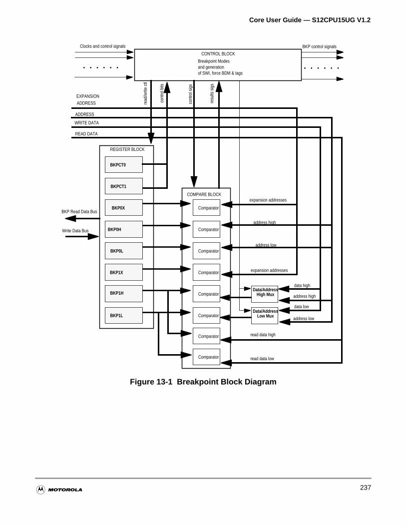
Core User Guide — S12CPU15UG V1.2
Figure 13-1 Breakpoint Block Diagram
Breakpoint Modesand generationof SWI, force BDM & tags
Comparator
BKP0H
BKP0L
BKP0X
BKPCT0
BKP1X
COMPARE BLOCK
REGISTER BLOCK
CONTROL BLOCK
BKPCT1
BKP1L
BKP1H
Comparator
Comparator
Comparator
Comparator
Comparator
Data/AddressHigh Mux
Data/AddressLow Mux
expansion addresses
expansion addresses
address high
address low
data high
data low
address high
address low
cont
rol s
igs
resu
lts s
igs
cont
rol b
its
read
/writ
e ct
l
ADDRESS
EXPANSIONADDRESS
WRITE DATA
Comparator
Comparator
read data high
read data low
READ DATA
. . . . . .
Clocks and control signals
BKP Read Data Bus
Write Data Bus
BKP control signals
. . . . . .
237
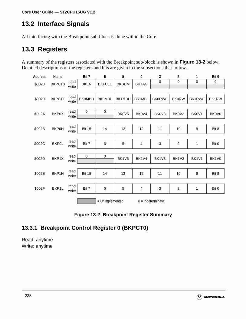
Core User Guide — S12CPU15UG V1.2
13.2 Interface Signals
All interfacing with the Breakpoint sub-block is done within the Core.
13.3 Registers
A summary of the registers associated with the Breakpoint sub-block is shown inFigure 13-2 below.Detailed descriptions of the registers and bits are given in the subsections that follow.
Figure 13-2 Breakpoint Register Summary
13.3.1 Breakpoint Control Register 0 (BKPCT0)
Read: anytimeWrite: anytime
Address Name Bit 7 6 5 4 3 2 1 Bit 0
$0028 BKPCT0read
BKEN BKFULL BKBDM BKTAG0 0 0 0
write
$0029 BKPCT1read
BK0MBH BK0MBL BK1MBH BK1MBL BK0RWE BK0RW BK1RWE BK1RWwrite
$002A BKP0Xread 0 0
BK0V5 BK0V4 BK0V3 BK0V2 BK0V1 BK0V0write
$002B BKP0Hread
Bit 15 14 13 12 11 10 9 Bit 8write
$002C BKP0Lread
Bit 7 6 5 4 3 2 1 Bit 0write
$002D BKP1Xread 0 0
BK1V5 BK1V4 BK1V3 BK1V2 BK1V1 BK1V0write
$002E BKP1Hread
Bit 15 14 13 12 11 10 9 Bit 8write
$002F BKP1Lread
Bit 7 6 5 4 3 2 1 Bit 0write
= Unimplemented X = Indeterminate
238
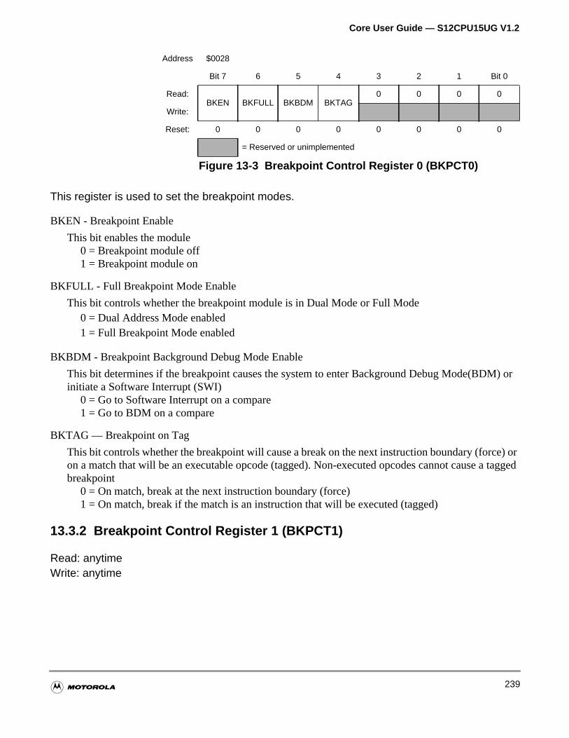
Core User Guide — S12CPU15UG V1.2
M) or
e) ora tagged
This register is used to set the breakpoint modes.
BKEN - Breakpoint Enable
This bit enables the module0 = Breakpoint module off1 = Breakpoint module on
BKFULL - Full Breakpoint Mode Enable
This bit controls whether the breakpoint module is in Dual Mode or Full Mode0 = Dual Address Mode enabled1 = Full Breakpoint Mode enabled
BKBDM - Breakpoint Background Debug Mode Enable
This bit determines if the breakpoint causes the system to enter Background Debug Mode(BDinitiate a Software Interrupt (SWI)
0 = Go to Software Interrupt on a compare1 = Go to BDM on a compare
BKTAG — Breakpoint on Tag
This bit controls whether the breakpoint will cause a break on the next instruction boundary (forcon a match that will be an executable opcode (tagged). Non-executed opcodes cannot cause breakpoint
0 = On match, break at the next instruction boundary (force)1 = On match, break if the match is an instruction that will be executed (tagged)
13.3.2 Breakpoint Control Register 1 (BKPCT1)
Read: anytimeWrite: anytime
Address $0028
Bit 7 6 5 4 3 2 1 Bit 0
Read:BKEN BKFULL BKBDM BKTAG
0 0 0 0
Write:
Reset: 0 0 0 0 0 0 0 0
= Reserved or unimplemented
Figure 13-3 Breakpoint Control Register 0 (BKPCT0)
239
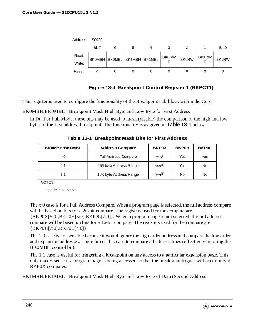
Core User Guide — S12CPU15UG V1.2
low
mpare
w ordering the
. Thisonly if
This register is used to configure the functionality of the Breakpoint sub-block within the Core.
BK0MBH:BK0MBL - Breakpoint Mask High Byte and Low Byte for First Address
In Dual or Full Mode, these bits may be used to mask (disable) the comparison of the high andbytes of the first address breakpoint. The functionality is as given inTable 13-1 below
The x:0 case is for a Full Address Compare. When a program page is selected, the full address cowill be based on bits for a 20-bit compare. The registers used for the compare are{BKP0X[5:0],BKP0H[5:0],BKP0L[7:0]}. When a program page is not selected, the full addresscompare will be based on bits for a 16-bit compare. The registers used for the compare are{BKP0H[7:0],BKP0L[7:0]}.
The 1:0 case is not sensible because it would ignore the high order address and compare the loand expansion addresses. Logic forces this case to compare all address lines (effectively ignorBK0MBH control bit).
The 1:1 case is useful for triggering a breakpoint on any access to a particular expansion pageonly makes sense if a program page is being accessed so that the breakpoint trigger will occurBKP0X compares.
BK1MBH:BK1MBL - Breakpoint Mask High Byte and Low Byte of Data (Second Address)
Address $0029
Bit 7 6 5 4 3 2 1 Bit 0
Read:BK0MBH BK0MBL BK1MBH BK1MBL
BK0RWE
BK0RWBK1RW
EBK1RW
Write:
Reset: 0 0 0 0 0 0 0 0
Figure 13-4 Breakpoint Control Register 1 (BKPCT1)
Table 13-1 Breakpoint Mask Bits for First Address
BK0MBH:BK0MBL Address Compare BKP0X BKP0H BKP0L
x:0 Full Address Compare Yes1
NOTES:
1. If page is selected.
Yes Yes
0:1 256 byte Address Range Yes(1) Yes No
1:1 16K byte Address Range Yes(1) No No
240
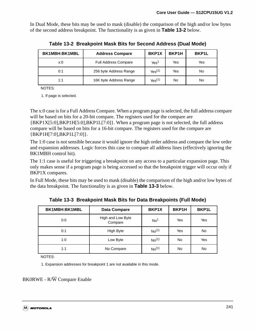
Core User Guide — S12CPU15UG V1.2
bytes
mpare
w ordering the
. Thisonly if
tes of
In Dual Mode, these bits may be used to mask (disable) the comparison of the high and/or lowof the second address breakpoint. The functionality is as given inTable 13-2 below.
The x:0 case is for a Full Address Compare. When a program page is selected, the full address cowill be based on bits for a 20-bit compare. The registers used for the compare are{BKP1X[5:0],BKP1H[5:0],BKP1L[7:0]}. When a program page is not selected, the full addresscompare will be based on bits for a 16-bit compare. The registers used for the compare are{BKP1H[7:0],BKP1L[7:0]}.
The 1:0 case is not sensible because it would ignore the high order address and compare the loand expansion addresses. Logic forces this case to compare all address lines (effectively ignorBK1MBH control bit).
The 1:1 case is useful for triggering a breakpoint on any access to a particular expansion pageonly makes sense if a program page is being accessed so that the breakpoint trigger will occurBKP1X compares.
In Full Mode, these bits may be used to mask (disable) the comparison of the high and/or low bythe data breakpoint. The functionality is as given inTable 13-3 below.
BK0RWE - R/W Compare Enable
Table 13-2 Breakpoint Mask Bits for Second Address (Dual Mode)
BK1MBH:BK1MBL Address Compare BKP1X BKP1H BKP1L
x:0 Full Address Compare Yes1
NOTES:
1. If page is selected.
Yes Yes
0:1 256 byte Address Range Yes(1) Yes No
1:1 16K byte Address Range Yes(1) No No
Table 13-3 Breakpoint Mask Bits for Data Breakpoints (Full Mode)
BK1MBH:BK1MBL Data Compare BKP1X BKP1H BKP1L
0:0High and Low Byte
Compare No1
NOTES:
1. Expansion addresses for breakpoint 1 are not available in this mode.
Yes Yes
0:1 High Byte No(1) Yes No
1:0 Low Byte No(1) No Yes
1:1 No Compare No(1) No No
241
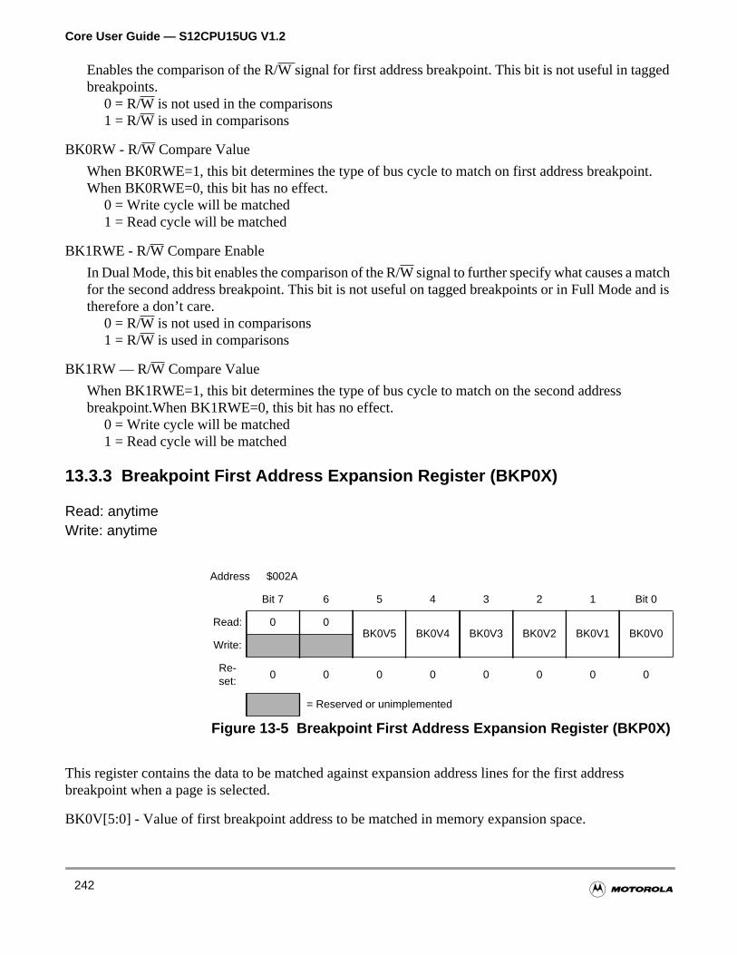
Core User Guide — S12CPU15UG V1.2
ed
int.
hnd is
s
Enables the comparison of the R/W signal for first address breakpoint. This bit is not useful in taggbreakpoints.
0 = R/W is not used in the comparisons1 = R/W is used in comparisons
BK0RW - R/W Compare Value
When BK0RWE=1, this bit determines the type of bus cycle to match on first address breakpoWhen BK0RWE=0, this bit has no effect.
0 = Write cycle will be matched1 = Read cycle will be matched
BK1RWE - R/W Compare Enable
In Dual Mode, this bit enables the comparison of the R/W signal to further specify what causes a matcfor the second address breakpoint. This bit is not useful on tagged breakpoints or in Full Mode atherefore a don’t care.
0 = R/W is not used in comparisons1 = R/W is used in comparisons
BK1RW — R/W Compare Value
When BK1RWE=1, this bit determines the type of bus cycle to match on the second addressbreakpoint.When BK1RWE=0, this bit has no effect.
0 = Write cycle will be matched1 = Read cycle will be matched
13.3.3 Breakpoint First Address Expansion Register (BKP0X)
Read: anytimeWrite: anytime
This register contains the data to be matched against expansion address lines for the first addresbreakpoint when a page is selected.
BK0V[5:0] - Value of first breakpoint address to be matched in memory expansion space.
Address $002A
Bit 7 6 5 4 3 2 1 Bit 0
Read: 0 0BK0V5 BK0V4 BK0V3 BK0V2 BK0V1 BK0V0
Write:
Re-set:
0 0 0 0 0 0 0 0
= Reserved or unimplemented
Figure 13-5 Breakpoint First Address Expansion Register (BKP0X)
242
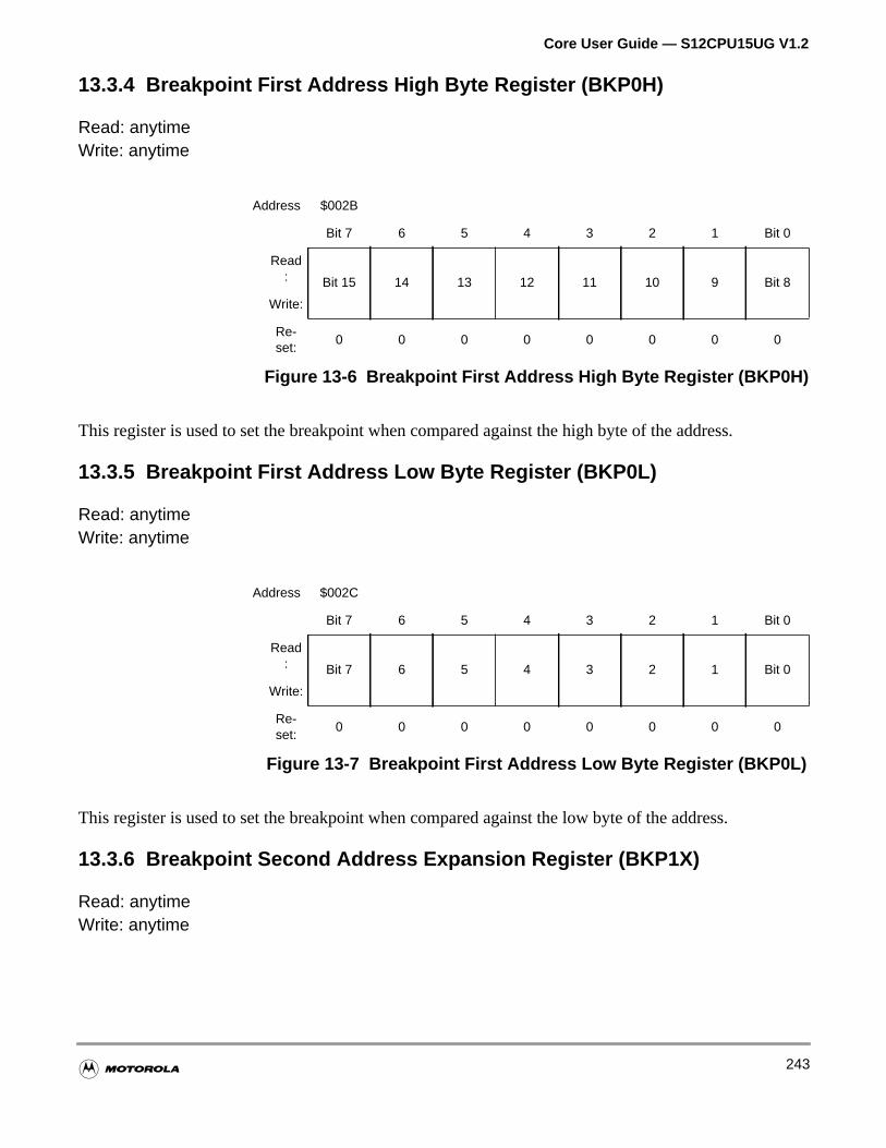
Core User Guide — S12CPU15UG V1.2
13.3.4 Breakpoint First Address High Byte Register (BKP0H)
Read: anytimeWrite: anytime
This register is used to set the breakpoint when compared against the high byte of the address.
13.3.5 Breakpoint First Address Low Byte Register (BKP0L)
Read: anytimeWrite: anytime
This register is used to set the breakpoint when compared against the low byte of the address.
13.3.6 Breakpoint Second Address Expansion Register (BKP1X)
Read: anytimeWrite: anytime
Address $002B
Bit 7 6 5 4 3 2 1 Bit 0
Read: Bit 15 14 13 12 11 10 9 Bit 8
Write:
Re-set:
0 0 0 0 0 0 0 0
Figure 13-6 Breakpoint First Address High Byte Register (BKP0H)
Address $002C
Bit 7 6 5 4 3 2 1 Bit 0
Read: Bit 7 6 5 4 3 2 1 Bit 0
Write:
Re-set:
0 0 0 0 0 0 0 0
Figure 13-7 Breakpoint First Address Low Byte Register (BKP0L)
243
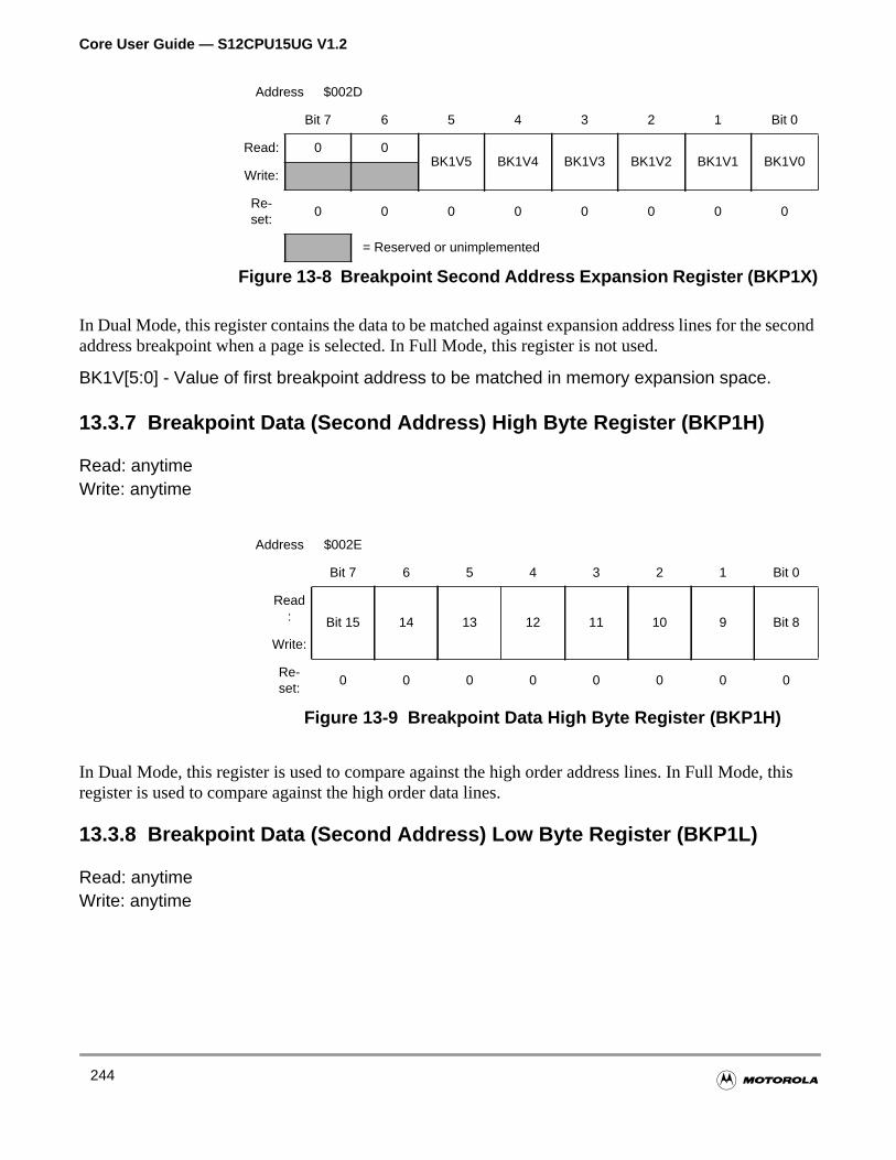
Core User Guide — S12CPU15UG V1.2
second
this
In Dual Mode, this register contains the data to be matched against expansion address lines for theaddress breakpoint when a page is selected. In Full Mode, this register is not used.
BK1V[5:0] - Value of first breakpoint address to be matched in memory expansion space.
13.3.7 Breakpoint Data (Second Address) High Byte Register (BKP1H)
Read: anytimeWrite: anytime
In Dual Mode, this register is used to compare against the high order address lines. In Full Mode,register is used to compare against the high order data lines.
13.3.8 Breakpoint Data (Second Address) Low Byte Register (BKP1L)
Read: anytimeWrite: anytime
Address $002D
Bit 7 6 5 4 3 2 1 Bit 0
Read: 0 0BK1V5 BK1V4 BK1V3 BK1V2 BK1V1 BK1V0
Write:
Re-set:
0 0 0 0 0 0 0 0
= Reserved or unimplemented
Figure 13-8 Breakpoint Second Address Expansion Register (BKP1X)
Address $002E
Bit 7 6 5 4 3 2 1 Bit 0
Read: Bit 15 14 13 12 11 10 9 Bit 8
Write:
Re-set:
0 0 0 0 0 0 0 0
Figure 13-9 Breakpoint Data High Byte Register (BKP1H)
244
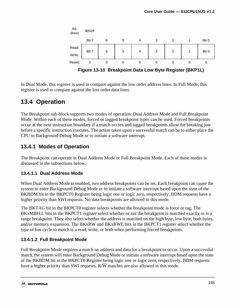
Core User Guide — S12CPU15UG V1.2
his
intpointsg justlace the
s is
use thef thee a
is abytes,
the
cessfulstatets
In Dual Mode, this register is used to compare against the low order address lines. In Full Mode, tregister is used to compare against the low order data lines.
13.4 Operation
The Breakpoint sub-block supports two modes of operation: Dual Address Mode and Full BreakpoMode. Within each of these modes, forced or tagged breakpoint types can be used. Forced breakoccur at the next instruction boundary if a match occurs and tagged breakpoints allow for breakinbefore a specific instruction executes. The action taken upon a successful match can be to either pCPU in Background Debug Mode or to initiate a software interrupt.
13.4.1 Modes of Operation
The Breakpoint can operate in Dual Address Mode or Full Breakpoint Mode. Each of these modediscussed in the subsections below.
13.4.1.1 Dual Address Mode
When Dual Address Mode is enabled, two address breakpoints can be set. Each breakpoint can casystem to enter Background Debug Mode or to initiate a software interrupt based upon the state oBKBDM bit in the BKPCT0 Register being logic one or logic zero, respectively. BDM requests havhigher priority than SWI requests. No data breakpoints are allowed in this mode.
The BKTAG bit in the BKPCT0 register selects whether the breakpoint mode is force or tag. TheBKxMBH:L bits in the BKPCT1 register select whether or not the breakpoint is matched exactly orrange breakpoint. They also select whether the address is matched on the high byte, low byte, bothand/or memory expansion. The BKxRW and BKxRWE bits in the BKPCT1 register select whethertype of bus cycle to match is a read, write, or both when performing forced breakpoints.
13.4.1.2 Full Breakpoint Mode
Full Breakpoint Mode requires a match on address and data for a breakpoint to occur. Upon a sucmatch, the system will enter Background Debug Mode or initiate a software interrupt based upon theof the BKBDM bit in the BKPCT0 Register being logic one or logic zero, respectively. BDM requeshave a higher priority than SWI requests. R/W matches are also allowed in this mode.
Ad-dress
$002F
Bit 7 6 5 4 3 2 1 Bit 0
Read:Bit 7 6 5 4 3 2 1 Bit 0
Write:
Reset: 0 0 0 0 0 0 0 0
Figure 13-10 Breakpoint Data Low Byte Register (BKP1L)
245
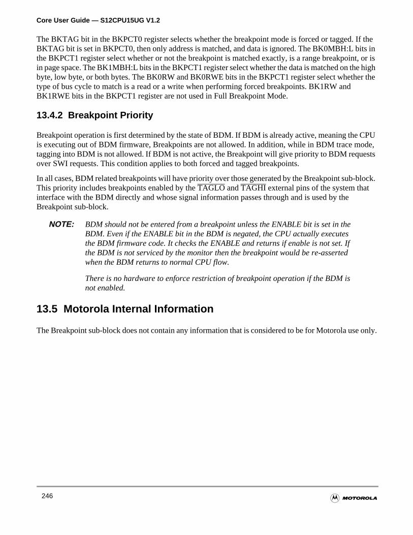
Core User Guide — S12CPU15UG V1.2
If thets int, or ise highr the
PUde,
ts
lock.
only.
The BKTAG bit in the BKPCT0 register selects whether the breakpoint mode is forced or tagged. BKTAG bit is set in BKPCT0, then only address is matched, and data is ignored. The BK0MBH:L bithe BKPCT1 register select whether or not the breakpoint is matched exactly, is a range breakpoinin page space. The BK1MBH:L bits in the BKPCT1 register select whether the data is matched on thbyte, low byte, or both bytes. The BK0RW and BK0RWE bits in the BKPCT1 register select whethetype of bus cycle to match is a read or a write when performing forced breakpoints. BK1RW andBK1RWE bits in the BKPCT1 register are not used in Full Breakpoint Mode.
13.4.2 Breakpoint Priority
Breakpoint operation is first determined by the state of BDM. If BDM is already active, meaning the Cis executing out of BDM firmware, Breakpoints are not allowed. In addition, while in BDM trace motagging into BDM is not allowed. If BDM is not active, the Breakpoint will give priority to BDM requesover SWI requests. This condition applies to both forced and tagged breakpoints.
In all cases, BDM related breakpoints will have priority over those generated by the Breakpoint sub-bThis priority includes breakpoints enabled by theTAGLO andTAGHI external pins of the system thatinterface with the BDM directly and whose signal information passes through and is used by theBreakpoint sub-block.
NOTE: BDM should not be entered from a breakpoint unless the ENABLE bit is set in theBDM. Even if the ENABLE bit in the BDM is negated, the CPU actually executesthe BDM firmware code. It checks the ENABLE and returns if enable is not set. Ifthe BDM is not serviced by the monitor then the breakpoint would be re-assertedwhen the BDM returns to normal CPU flow.
There is no hardware to enforce restriction of breakpoint operation if the BDM isnot enabled.
13.5 Motorola Internal Information
The Breakpoint sub-block does not contain any information that is considered to be for Motorola use
246
Core User Guide — S12CPU15UG V1.2
ore.
entedD
Section 14 Background Debug Mode (BDM)
This section describes the functionality of the Background Debug Mode (BDM) sub-block of the C
14.1 Overview
The Background Debug Mode (BDM) sub-block is a single-wire, background debug system implemin on-chip hardware for minimal CPU intervention. All interfacing with the BDM is done via the BKGpin.
14.1.1 Features
• Single-wire communication with host development system
• Active out of reset in special single-chip mode
• Nine hardware commands using free cycles, if available, for minimal CPU intervention
• Hardware commands not requiring active BDM
• 15 firmware commands execute from the standard BDM firmware lookup table
• Instruction tagging capability
• Software control of BDM operation during wait mode
• Software selectable clocks
• BDM disabled when secure feature is enabled
247
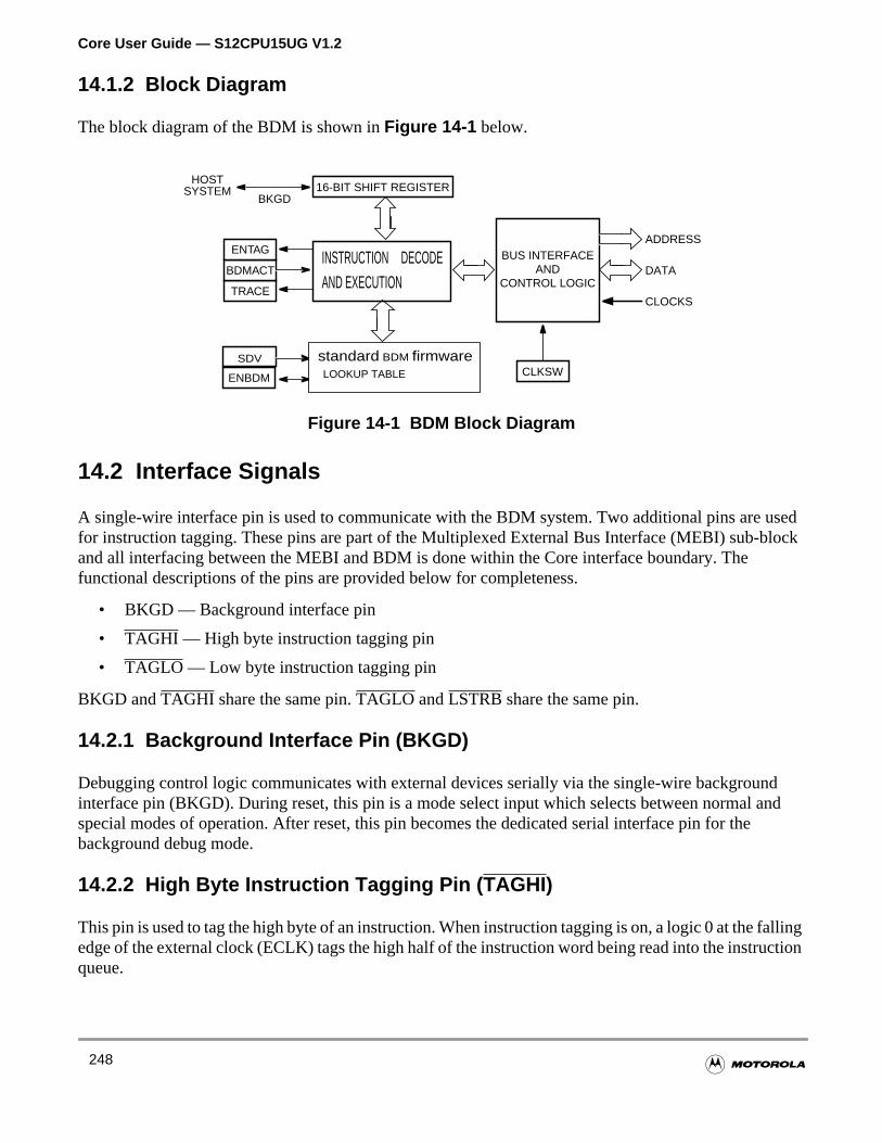
Core User Guide — S12CPU15UG V1.2
usedlock
ndand
llingction
14.1.2 Block Diagram
The block diagram of the BDM is shown inFigure 14-1 below.
Figure 14-1 BDM Block Diagram
14.2 Interface Signals
A single-wire interface pin is used to communicate with the BDM system. Two additional pins are for instruction tagging. These pins are part of the Multiplexed External Bus Interface (MEBI) sub-band all interfacing between the MEBI and BDM is done within the Core interface boundary. Thefunctional descriptions of the pins are provided below for completeness.
• BKGD — Background interface pin
• TAGHI — High byte instruction tagging pin
• TAGLO — Low byte instruction tagging pin
BKGD andTAGHI share the same pin.TAGLO andLSTRB share the same pin.
14.2.1 Background Interface Pin (BKGD)
Debugging control logic communicates with external devices serially via the single-wire backgrouinterface pin (BKGD). During reset, this pin is a mode select input which selects between normal special modes of operation. After reset, this pin becomes the dedicated serial interface pin for thebackground debug mode.
14.2.2 High Byte Instruction Tagging Pin ( TAGHI)
This pin is used to tag the high byte of an instruction. When instruction tagging is on, a logic 0 at the faedge of the external clock (ECLK) tags the high half of the instruction word being read into the instruqueue.
ENBDM CLKSW
BDMACT
ENTAG
TRACE
SDV
16-BIT SHIFT REGISTERBKGD
CLOCKS
DATA
ADDRESS
HOSTSYSTEM
BUS INTERFACEAND
CONTROL LOGICAND EXECUTIONINSTRUCTION DECODE
LOOKUP TABLE
standard BDM firmware
248
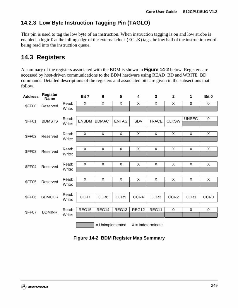
Core User Guide — S12CPU15UG V1.2
e isord
that
14.2.3 Low Byte Instruction Tagging Pin ( TAGLO)
This pin is used to tag the low byte of an instruction. When instruction tagging is on and low strobenabled, a logic 0 at the falling edge of the external clock (ECLK) tags the low half of the instruction wbeing read into the instruction queue.
14.3 Registers
A summary of the registers associated with the BDM is shown inFigure 14-2 below. Registers areaccessed by host-driven communications to the BDM hardware using READ_BD and WRITE_BDcommands. Detailed descriptions of the registers and associated bits are given in the subsectionsfollow.
Figure 14-2 BDM Register Map Summary
Address RegisterName Bit 7 6 5 4 3 2 1 Bit 0
$FF00 ReservedRead: X X X X X X 0 0Write:
$FF01 BDMSTSRead:
ENBDM BDMACT ENTAG SDV TRACE CLKSWUNSEC 0
Write:
$FF02 ReservedRead: X X X X X X X XWrite:
$FF03 ReservedRead: X X X X X X X XWrite:
$FF04 ReservedRead: X X X X X X X XWrite:
$FF05 ReservedRead: X X X X X X X XWrite:
$FF06 BDMCCRRead:
CCR7 CCR6 CCR5 CCR4 CCR3 CCR2 CCR1 CCR0Write:
$FF07 BDMINRRead: REG15 REG14 REG13 REG12 REG11 0 0 0Write:
= Unimplemented X = Indeterminate
249
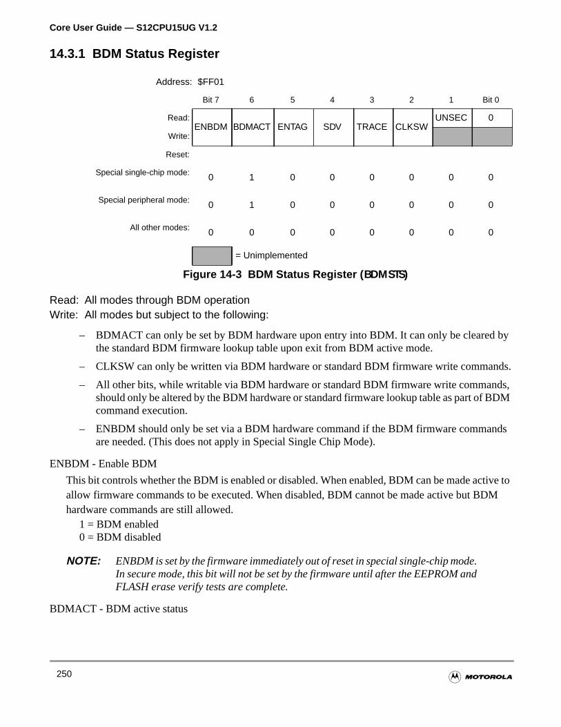
Core User Guide — S12CPU15UG V1.2
by
nds.
s,DM
nds
ive toDM
14.3.1 BDM Status Register
Read: All modes through BDM operationWrite: All modes but subject to the following:
– BDMACT can only be set by BDM hardware upon entry into BDM. It can only be clearedthe standard BDM firmware lookup table upon exit from BDM active mode.
– CLKSW can only be written via BDM hardware or standard BDM firmware write comma
– All other bits, while writable via BDM hardware or standard BDM firmware write commandshould only be altered by the BDM hardware or standard firmware lookup table as part of Bcommand execution.
– ENBDM should only be set via a BDM hardware command if the BDM firmware commaare needed. (This does not apply in Special Single Chip Mode).
ENBDM - Enable BDM
This bit controls whether the BDM is enabled or disabled. When enabled, BDM can be made actallow firmware commands to be executed. When disabled, BDM cannot be made active but Bhardware commands are still allowed.
1 = BDM enabled0 = BDM disabled
NOTE: ENBDM is set by the firmware immediately out of reset in special single-chip mode.In secure mode, this bit will not be set by the firmware until after the EEPROM andFLASH erase verify tests are complete.
BDMACT - BDM active status
Address: $FF01
Bit 7 6 5 4 3 2 1 Bit 0
Read:ENBDM BDMACT ENTAG SDV TRACE CLKSW
UNSEC 0
Write:
Reset:
Special single-chip mode: 0 1 0 0 0 0 0 0
Special peripheral mode: 0 1 0 0 0 0 0 0
All other modes: 0 0 0 0 0 0 0 0
= Unimplemented
Figure 14-3 BDM Status Register (BDMSTS)
250
Core User Guide — S12CPU15UG V1.2
abled
M
e tag
art of a. It ise
onge next
eheBDM
This bit becomes set upon entering BDM. The standard BDM firmware lookup table is then enand put into the memory map. BDMACT is cleared by a carefully timed store instruction in thestandard BDM firmware as part of the exit sequence to return to user code and remove the BDmemory from the map.
1 = BDM active0 = BDM not active
ENTAG - Tagging enable
This bit indicates whether instruction tagging in enabled or disabled. It is set when the TAGGOcommand is executed and cleared when BDM is entered. The serial system is disabled and thfunction enabled 16 cycles after this bit is written. BDM cannot process serial commands whiletagging is active.
1 = Tagging enabled0 = Tagging not enabled, or BDM active
SDV - Shift data valid
This bit is set and cleared by the BDM hardware. It is set after data has been transmitted as pfirmware read command or after data has been received as part of a firmware write commandcleared when the next BDM command has been received or BDM is exited. SDV is used by thstandard BDM firmware to control program flow execution.
1 = Data phase of command is complete0 = Data phase of command not complete
TRACE - TRACE1 BDM firmware command is being executed
This bit gets set when a BDM TRACE1 firmware command is first recognized. It will stay set as las continuous back-to-back TRACE1 commands are executed. This bit will get cleared when thcommand that is not a TRACE1 command is recognized.
1 = TRACE1 command is being executed0 = TRACE1 command is not being executed
CLKSW - Clock switch
The CLKSW bit controls which clock the BDM operates with. It is only writable from a hardwarBDM command. A 150 cycle delay at the clock speed that is active during the data portion of tcommand will occur before the new clock source is guaranteed to be active. The start of the nextcommand uses the new clock for timing subsequent BDM communications.
1 = BDM system operates with bus rate0 = BDM system operates with alternate clock
WARNING:The BDM will not operate with CLKSW = 0 if the frequency of the alternate clocksource, peri_phase_oscdX, is greater than one half of the bus frequency. Pleaserefer to the users guide for the clock generation module to determine if thiscondition can occur.
UNSEC - Unsecure
251
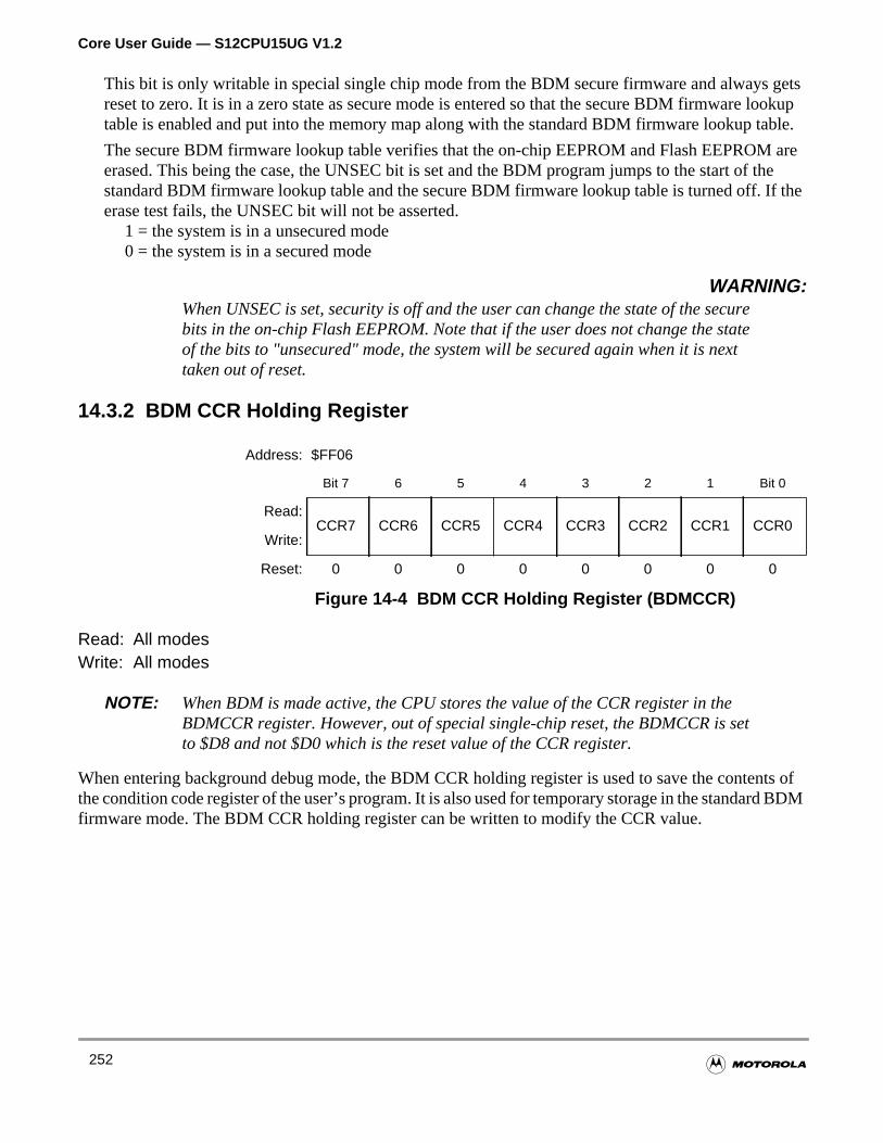
Core User Guide — S12CPU15UG V1.2
getslookupable.
arethethe
nts ofBDM
This bit is only writable in special single chip mode from the BDM secure firmware and alwaysreset to zero. It is in a zero state as secure mode is entered so that the secure BDM firmware table is enabled and put into the memory map along with the standard BDM firmware lookup t
The secure BDM firmware lookup table verifies that the on-chip EEPROM and Flash EEPROMerased. This being the case, the UNSEC bit is set and the BDM program jumps to the start of standard BDM firmware lookup table and the secure BDM firmware lookup table is turned off. Iferase test fails, the UNSEC bit will not be asserted.
1 = the system is in a unsecured mode0 = the system is in a secured mode
WARNING:When UNSEC is set, security is off and the user can change the state of the securebits in the on-chip Flash EEPROM. Note that if the user does not change the stateof the bits to "unsecured" mode, the system will be secured again when it is nexttaken out of reset.
14.3.2 BDM CCR Holding Register
Read: All modesWrite: All modes
NOTE: When BDM is made active, the CPU stores the value of the CCR register in theBDMCCR register. However, out of special single-chip reset, the BDMCCR is setto $D8 and not $D0 which is the reset value of the CCR register.
When entering background debug mode, the BDM CCR holding register is used to save the contethe condition code register of the user’s program. It is also used for temporary storage in the standardfirmware mode. The BDM CCR holding register can be written to modify the CCR value.
Address: $FF06
Bit 7 6 5 4 3 2 1 Bit 0
Read:CCR7 CCR6 CCR5 CCR4 CCR3 CCR2 CCR1 CCR0
Write:
Reset: 0 0 0 0 0 0 0 0
Figure 14-4 BDM CCR Holding Register (BDMCCR)
252
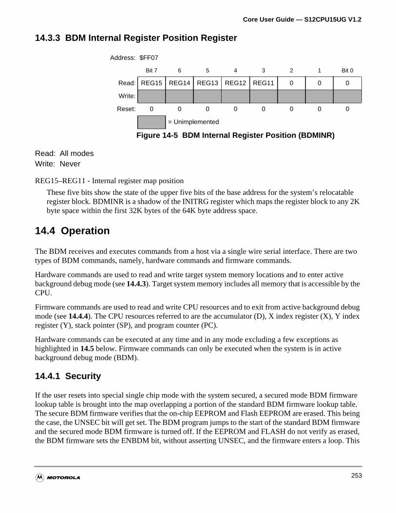
Core User Guide — S12CPU15UG V1.2
table2K
re two
ivethe
debugdex
s
mwareable.beingare
sed,This
14.3.3 BDM Internal Register Position Register
Read: All modesWrite: Never
REG15–REG11 - Internal register map position
These five bits show the state of the upper five bits of the base address for the system’s relocaregister block. BDMINR is a shadow of the INITRG register which maps the register block to anybyte space within the first 32K bytes of the 64K byte address space.
14.4 Operation
The BDM receives and executes commands from a host via a single wire serial interface. There atypes of BDM commands, namely, hardware commands and firmware commands.
Hardware commands are used to read and write target system memory locations and to enter actbackground debug mode (see14.4.3). Target system memory includes all memory that is accessible byCPU.
Firmware commands are used to read and write CPU resources and to exit from active backgroundmode (see14.4.4). The CPU resources referred to are the accumulator (D), X index register (X), Y inregister (Y), stack pointer (SP), and program counter (PC).
Hardware commands can be executed at any time and in any mode excluding a few exceptions ahighlighted in14.5 below. Firmware commands can only be executed when the system is in activebackground debug mode (BDM).
14.4.1 Security
If the user resets into special single chip mode with the system secured, a secured mode BDM firlookup table is brought into the map overlapping a portion of the standard BDM firmware lookup tThe secure BDM firmware verifies that the on-chip EEPROM and Flash EEPROM are erased. Thisthe case, the UNSEC bit will get set. The BDM program jumps to the start of the standard BDM firmwand the secured mode BDM firmware is turned off. If the EEPROM and FLASH do not verify as erathe BDM firmware sets the ENBDM bit, without asserting UNSEC, and the firmware enters a loop.
Address: $FF07
Bit 7 6 5 4 3 2 1 Bit 0
Read: REG15 REG14 REG13 REG12 REG11 0 0 0
Write:
Reset: 0 0 0 0 0 0 0 0
= Unimplemented
Figure 14-5 BDM Internal Register Position (BDMINR)
253
Core User Guide — S12CPU15UG V1.2
mands.
vated
e
ng the
of the
sesegistersrams.
iveU such
tem to a
ss doesPU
ationwever,
causes the BDM hardware commands to become enabled, but does not enable the software comThis allows the BDM hardware to be used to erase the EEPROM and FLASH.
14.4.2 Enabling and Activating BDM
The system must be in active BDM to execute standard BDM firmware commands. BDM can be actionly after being enabled. BDM is enabled by setting the ENBDM bit in the BDM status (BDMSTS)register. The ENBDM bit is set by writing to the BDM status (BDMSTS) register, via the single-wirinterface, using a hardware command such as WRITE_BD_BYTE.
After being enabled, BDM is activated by one of the following1:
• Hardware BACKGROUND command
• BDM external instruction tagging mechanism
• CPU BGND instruction
• Breakpoint sub-block’s force or tag mechanism2
When BDM is activated, the CPU finishes executing the current instruction and then begins executifirmware in the standard BDM firmware lookup table. When BDM is activated by the breakpointsub-block, the type of breakpoint used determines if BDM becomes active before or after executionnext instruction.
NOTE: If an attempt is made to activate BDM before being enabled, the CPU resumesnormal instruction execution after a brief delay. If BDM is not enabled, anyhardware BACKGROUND commands issued are ignored by the BDM and the CPUis not delayed.
In active BDM, the BDM registers and standard BDM firmware lookup table are mapped to addres$FF00 to $FFFF. BDM registers are mapped to addresses $FF00 to $FF07. The BDM uses these rwhich are readable anytime by the BDM. These registers are not, however, readable by user prog
14.4.3 BDM Hardware Commands
Hardware commands are used to read and write target system memory locations and to enter actbackground debug mode. Target system memory includes all memory that is accessible by the CPas on-chip RAM, EEPROM, Flash EEPROM, I/O and control registers, and all external memory.
Hardware commands are executed with minimal or no CPU intervention and do not require the sysbe in active BDM for execution, although, they can still be executed in this mode. When executinghardware command, the BDM sub-block waits for a free CPU bus cycle so that the background accenot disturb the running application program. If a free cycle is not found within 128 clock cycles, the Cis momentarily frozen so that the BDM can steal a cycle. When the BDM finds a free cycle, the operdoes not intrude on normal CPU operation provided that it can be completed in a single cycle. Ho
NOTES:1. BDM is enabled and active immediately out of special single-chip reset (see 14.5.2).2. This method is only available on systems that have a a Breakpoint sub-block.
254
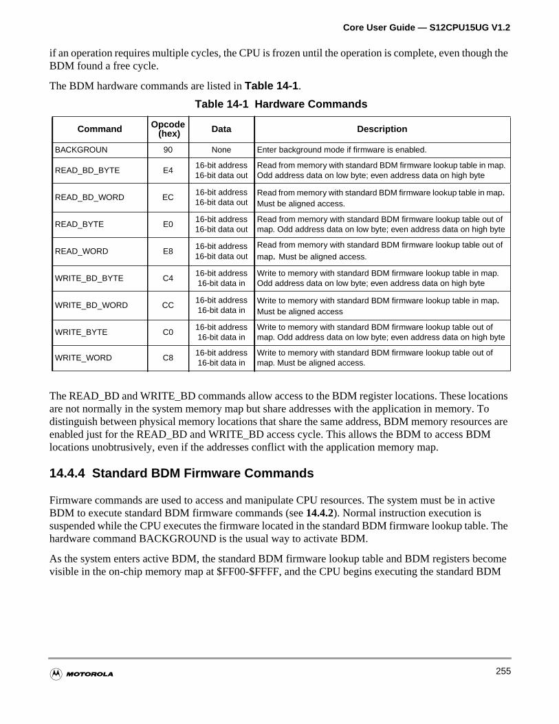
Core User Guide — S12CPU15UG V1.2
h the
tions Toces are
active
. The
comeBDM
if an operation requires multiple cycles, the CPU is frozen until the operation is complete, even thougBDM found a free cycle.
The BDM hardware commands are listed inTable 14-1 .
The READ_BD and WRITE_BD commands allow access to the BDM register locations. These locaare not normally in the system memory map but share addresses with the application in memory.distinguish between physical memory locations that share the same address, BDM memory resourenabled just for the READ_BD and WRITE_BD access cycle. This allows the BDM to access BDMlocations unobtrusively, even if the addresses conflict with the application memory map.
14.4.4 Standard BDM Firmware Commands
Firmware commands are used to access and manipulate CPU resources. The system must be inBDM to execute standard BDM firmware commands (see14.4.2). Normal instruction execution issuspended while the CPU executes the firmware located in the standard BDM firmware lookup tablehardware command BACKGROUND is the usual way to activate BDM.
As the system enters active BDM, the standard BDM firmware lookup table and BDM registers bevisible in the on-chip memory map at $FF00-$FFFF, and the CPU begins executing the standard
Table 14-1 Hardware Commands
Command Opcode (hex) Data Description
BACKGROUN 90 None Enter background mode if firmware is enabled.
READ_BD_BYTE E416-bit address16-bit data out
Read from memory with standard BDM firmware lookup table in map.Odd address data on low byte; even address data on high byte
READ_BD_WORD EC16-bit address16-bit data out
Read from memory with standard BDM firmware lookup table in map.Must be aligned access.
READ_BYTE E016-bit address16-bit data out
Read from memory with standard BDM firmware lookup table out ofmap. Odd address data on low byte; even address data on high byte
READ_WORD E816-bit address16-bit data out
Read from memory with standard BDM firmware lookup table out ofmap. Must be aligned access.
WRITE_BD_BYTE C416-bit address16-bit data in
Write to memory with standard BDM firmware lookup table in map.Odd address data on low byte; even address data on high byte
WRITE_BD_WORD CC16-bit address16-bit data in
Write to memory with standard BDM firmware lookup table in map.Must be aligned access
WRITE_BYTE C016-bit address16-bit data in
Write to memory with standard BDM firmware lookup table out ofmap. Odd address data on low byte; even address data on high byte
WRITE_WORD C816-bit address16-bit data in
Write to memory with standard BDM firmware lookup table out ofmap. Must be aligned access.
255
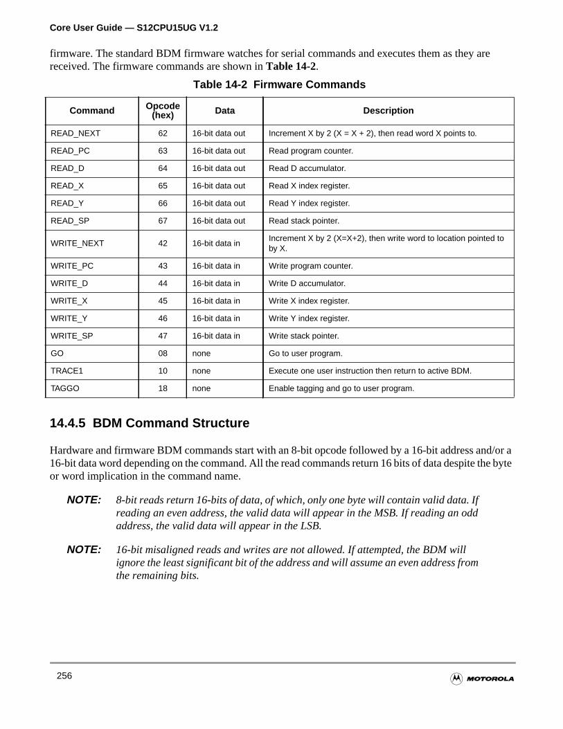
Core User Guide — S12CPU15UG V1.2
re
d/or ae byte
firmware. The standard BDM firmware watches for serial commands and executes them as they areceived. The firmware commands are shown inTable 14-2.
14.4.5 BDM Command Structure
Hardware and firmware BDM commands start with an 8-bit opcode followed by a 16-bit address an16-bit data word depending on the command. All the read commands return 16 bits of data despite thor word implication in the command name.
NOTE: 8-bit reads return 16-bits of data, of which, only one byte will contain valid data. Ifreading an even address, the valid data will appear in the MSB. If reading an oddaddress, the valid data will appear in the LSB.
NOTE: 16-bit misaligned reads and writes are not allowed. If attempted, the BDM willignore the least significant bit of the address and will assume an even address fromthe remaining bits.
Table 14-2 Firmware Commands
Command Opcode(hex) Data Description
READ_NEXT 62 16-bit data out Increment X by 2 (X = X + 2), then read word X points to.
READ_PC 63 16-bit data out Read program counter.
READ_D 64 16-bit data out Read D accumulator.
READ_X 65 16-bit data out Read X index register.
READ_Y 66 16-bit data out Read Y index register.
READ_SP 67 16-bit data out Read stack pointer.
WRITE_NEXT 42 16-bit data inIncrement X by 2 (X=X+2), then write word to location pointed toby X.
WRITE_PC 43 16-bit data in Write program counter.
WRITE_D 44 16-bit data in Write D accumulator.
WRITE_X 45 16-bit data in Write X index register.
WRITE_Y 46 16-bit data in Write Y index register.
WRITE_SP 47 16-bit data in Write stack pointer.
GO 08 none Go to user program.
TRACE1 10 none Execute one user instruction then return to active BDM.
TAGGO 18 none Enable tagging and go to user program.
256
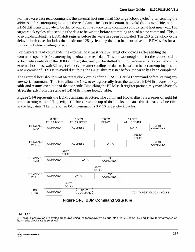
Core User Guide — S12CPU15UG V1.2
in theit 150This iscycle for a
ed datas, theo sendpleted.
g anykupersely
ht bitidles
For hardware data read commands, the external host must wait 150 target clock cycles1 after sending theaddress before attempting to obtain the read data. This is to be certain that valid data is availableBDM shift register, ready to be shifted out. For hardware write commands, the external host must watarget clock cycles after sending the data to be written before attempting to send a new command.to avoid disturbing the BDM shift register before the write has been completed. The 150 target clockdelay in both cases includes the maximum 128 cycle delay that can be incurred as the BDM waitsfree cycle before stealing a cycle.
For firmware read commands, the external host must wait 32 target clock cycles after sending thecommand opcode before attempting to obtain the read data. This allows enough time for the requestto be made available in the BDM shift register, ready to be shifted out. For firmware write commandexternal host must wait 32 target clock cycles after sending the data to be written before attempting ta new command. This is to avoid disturbing the BDM shift register before the write has been com
The external host should wait 64 target clock cycles after a TRACE1 or GO command before startinnew serial command. This is to allow the CPU to exit gracefully from the standard BDM firmware lootable and resume execution of the user code. Disturbing the BDM shift register prematurely may advaffect the exit from the standard BDM firmware lookup table.
Figure 14-6represents the BDM command structure. The command blocks illustrate a series of eigtimes starting with a falling edge. The bar across the top of the blocks indicates that the BKGD linein the high state. The time for an 8-bit command is 8× 16 target clock cycles.
Figure 14-6 BDM Command Structure
NOTES:1. Target clock cycles are cycles measured using the target system’s serial clock rate. See 14.4.6 and 14.3.1 for information onhow serial clock rate is selected.
HARDWARE
HARDWARE
FIRMWARE
FIRMWARE
GO,
32-TC
TC = TARGET CLOCK CYCLES
COMMAND ADDRESS
150-TCDELAY
NEXT
DELAY
8 BITSAT ~16 TC/BIT
16 BITSAT ~16 TC/BIT
16 BITSAT ~16 TC/BIT
COMMAND ADDRESS DATANEXT
DATAREAD
WRITE
READ
WRITE
TRACE
COMMANDNEXT
COMMAND DATA
64-TCDELAY
NEXT
COMMAND
150-TCDELAY
32-TCDELAY
COMMAND
COMMAND
COMMAND
COMMANDDATA
NEXTCOMMAND
257
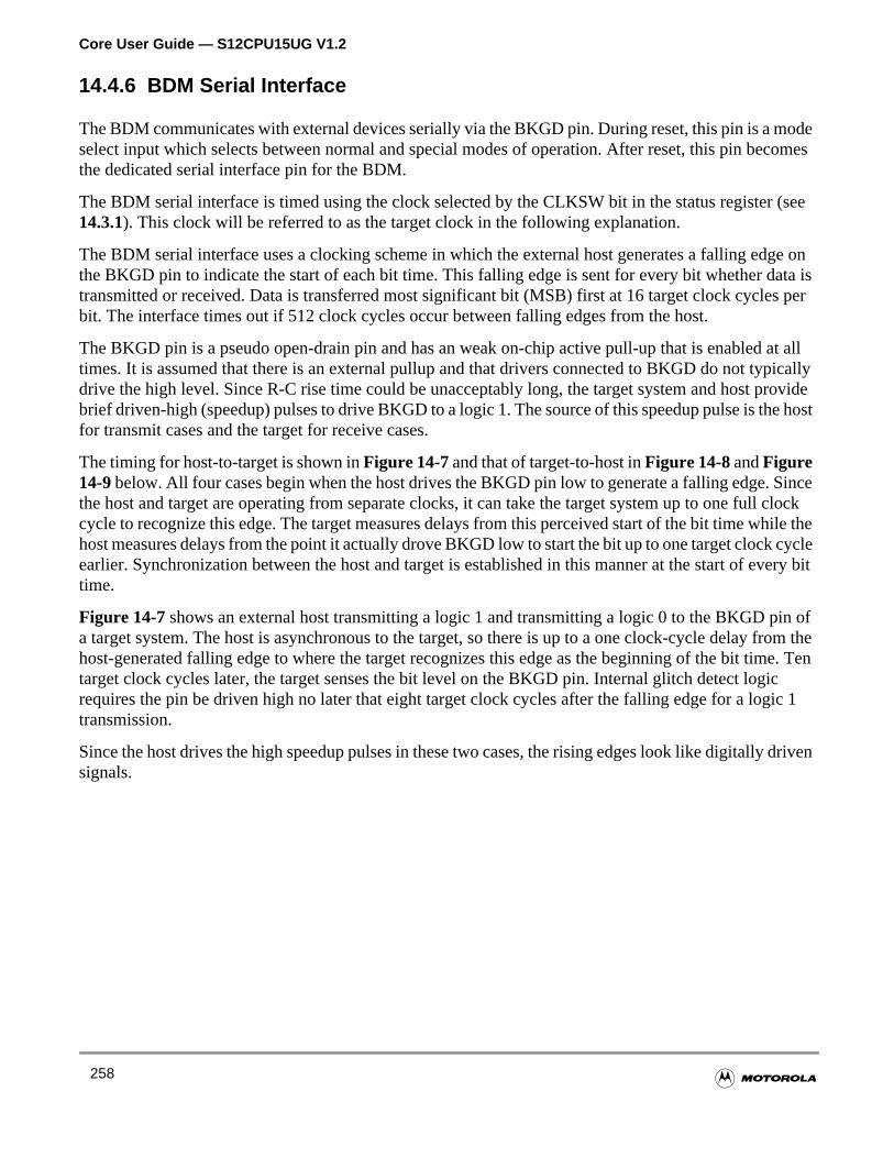
Core User Guide — S12CPU15UG V1.2
odecomes
(see
ge onta iss per
at allpicallyrovidee host
incel clockile thecyclevery bit
in ofom thee. Ten
icic 1
driven
14.4.6 BDM Serial Interface
The BDM communicates with external devices serially via the BKGD pin. During reset, this pin is a mselect input which selects between normal and special modes of operation. After reset, this pin bethe dedicated serial interface pin for the BDM.
The BDM serial interface is timed using the clock selected by the CLKSW bit in the status register14.3.1). This clock will be referred to as the target clock in the following explanation.
The BDM serial interface uses a clocking scheme in which the external host generates a falling edthe BKGD pin to indicate the start of each bit time. This falling edge is sent for every bit whether datransmitted or received. Data is transferred most significant bit (MSB) first at 16 target clock cyclebit. The interface times out if 512 clock cycles occur between falling edges from the host.
The BKGD pin is a pseudo open-drain pin and has an weak on-chip active pull-up that is enabledtimes. It is assumed that there is an external pullup and that drivers connected to BKGD do not tydrive the high level. Since R-C rise time could be unacceptably long, the target system and host pbrief driven-high (speedup) pulses to drive BKGD to a logic 1. The source of this speedup pulse is thfor transmit cases and the target for receive cases.
The timing for host-to-target is shown inFigure 14-7and that of target-to-host inFigure 14-8andFigure14-9below. All four cases begin when the host drives the BKGD pin low to generate a falling edge. Sthe host and target are operating from separate clocks, it can take the target system up to one fulcycle to recognize this edge. The target measures delays from this perceived start of the bit time whhost measures delays from the point it actually drove BKGD low to start the bit up to one target clockearlier. Synchronization between the host and target is established in this manner at the start of etime.
Figure 14-7 shows an external host transmitting a logic 1 and transmitting a logic 0 to the BKGD pa target system. The host is asynchronous to the target, so there is up to a one clock-cycle delay frhost-generated falling edge to where the target recognizes this edge as the beginning of the bit timtarget clock cycles later, the target senses the bit level on the BKGD pin. Internal glitch detect logrequires the pin be driven high no later that eight target clock cycles after the falling edge for a logtransmission.
Since the host drives the high speedup pulses in these two cases, the rising edges look like digitallysignals.
258
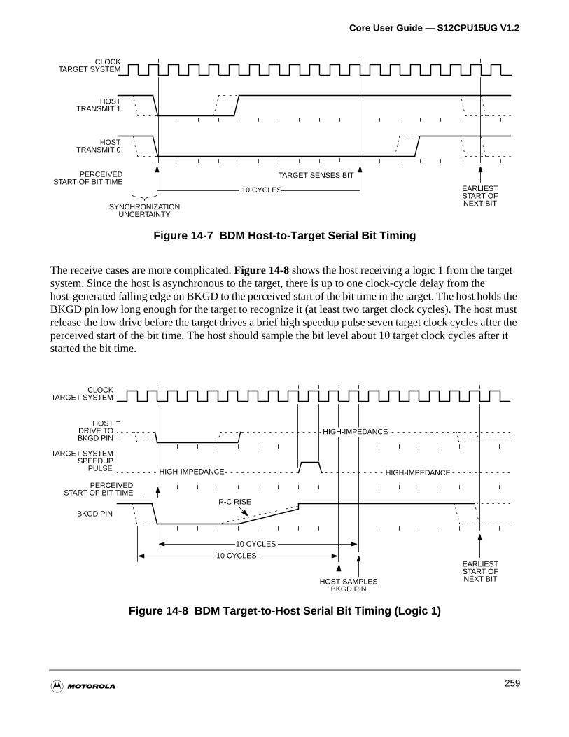
Core User Guide — S12CPU15UG V1.2
t
ds themustfter thefter it
Figure 14-7 BDM Host-to-Target Serial Bit Timing
The receive cases are more complicated.Figure 14-8 shows the host receiving a logic 1 from the targesystem. Since the host is asynchronous to the target, there is up to one clock-cycle delay from thehost-generated falling edge on BKGD to the perceived start of the bit time in the target. The host holBKGD pin low long enough for the target to recognize it (at least two target clock cycles). The hostrelease the low drive before the target drives a brief high speedup pulse seven target clock cycles aperceived start of the bit time. The host should sample the bit level about 10 target clock cycles astarted the bit time.
Figure 14-8 BDM Target-to-Host Serial Bit Timing (Logic 1)
EARLIESTSTART OFNEXT BIT
TARGET SENSES BIT
10 CYCLES
SYNCHRONIZATIONUNCERTAINTY
CLOCKTARGET SYSTEM
HOSTTRANSMIT 1
HOSTTRANSMIT 0
PERCEIVEDSTART OF BIT TIME
HIGH-IMPEDANCE
EARLIESTSTART OFNEXT BIT
R-C RISE
10 CYCLES
10 CYCLES
HOST SAMPLESBKGD PIN
PERCEIVEDSTART OF BIT TIME
BKGD PIN
CLOCKTARGET SYSTEM
HOSTDRIVE TOBKGD PIN
TARGET SYSTEMSPEEDUP
PULSE
HIGH-IMPEDANCE
HIGH-IMPEDANCE
259
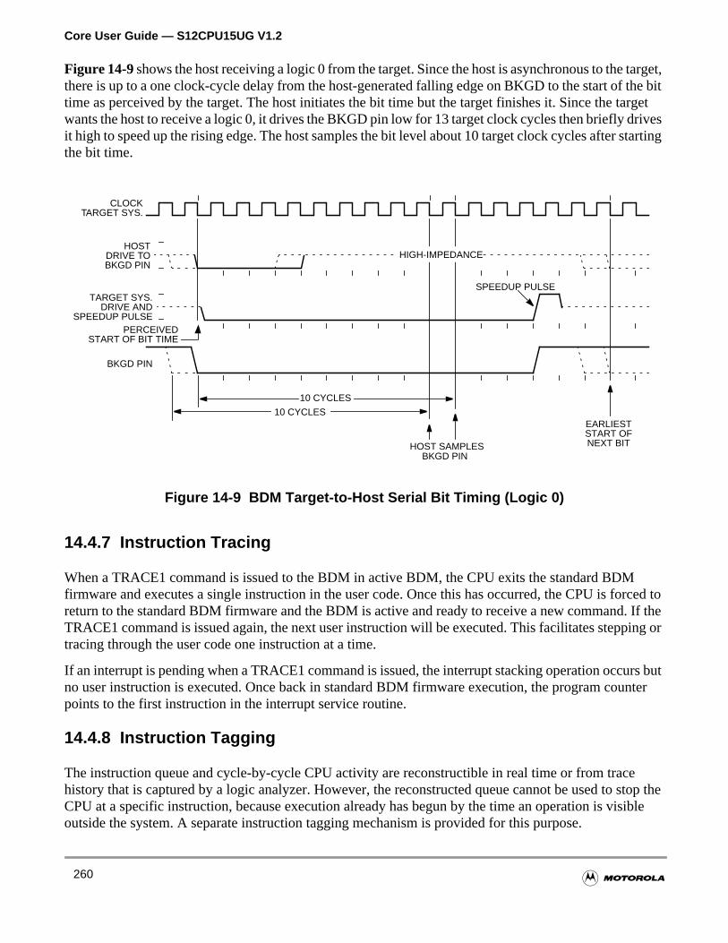
Core User Guide — S12CPU15UG V1.2
arget,he bitargetivestarting
rced toIf theing or
rs butnter
estop thesible
Figure 14-9shows the host receiving a logic 0 from the target. Since the host is asynchronous to the tthere is up to a one clock-cycle delay from the host-generated falling edge on BKGD to the start of ttime as perceived by the target. The host initiates the bit time but the target finishes it. Since the twants the host to receive a logic 0, it drives the BKGD pin low for 13 target clock cycles then briefly drit high to speed up the rising edge. The host samples the bit level about 10 target clock cycles after sthe bit time.
Figure 14-9 BDM Target-to-Host Serial Bit Timing (Logic 0)
14.4.7 Instruction Tracing
When a TRACE1 command is issued to the BDM in active BDM, the CPU exits the standard BDMfirmware and executes a single instruction in the user code. Once this has occurred, the CPU is foreturn to the standard BDM firmware and the BDM is active and ready to receive a new command.TRACE1 command is issued again, the next user instruction will be executed. This facilitates stepptracing through the user code one instruction at a time.
If an interrupt is pending when a TRACE1 command is issued, the interrupt stacking operation occuno user instruction is executed. Once back in standard BDM firmware execution, the program coupoints to the first instruction in the interrupt service routine.
14.4.8 Instruction Tagging
The instruction queue and cycle-by-cycle CPU activity are reconstructible in real time or from trachistory that is captured by a logic analyzer. However, the reconstructed queue cannot be used to CPU at a specific instruction, because execution already has begun by the time an operation is vioutside the system. A separate instruction tagging mechanism is provided for this purpose.
EARLIESTSTART OFNEXT BIT
CLOCKTARGET SYS.
HOSTDRIVE TOBKGD PIN
BKGD PIN
PERCEIVEDSTART OF BIT TIME
10 CYCLES
10 CYCLES
HOST SAMPLESBKGD PIN
TARGET SYS.DRIVE AND
SPEEDUP PULSE
SPEEDUP PULSE
HIGH-IMPEDANCE
260
Core User Guide — S12CPU15UG V1.2
ruction.
statehe fallow
s and
cuted.
during
ACTs the
The tag follows program information as it advances through the instruction queue. When a taggedinstruction reaches the head of the queue, the CPU enters active BDM rather than executing the inst
NOTE: Tagging is disabled when BDM becomes active and BDM serial commands are notprocessed while tagging is active.
Executing the BDM TAGGO command configures two system pins for tagging. TheTAGLO signalshares a pin with theLSTRB signal, and theTAGHI signal shares a pin with the BKGD signal.
Table 14-3shows the functions of the two tagging pins. The pins operate independently, that is, theof one pin does not affect the function of the other. The presence of logic level 0 on either pin at tof the external clock (ECLK) performs the indicated function. High tagging is allowed in all modes. Ltagging is allowed only when low strobe is enabled (LSTRB is allowed only in wide expanded modeemulation expanded narrow mode).
14.5 Modes of Operation
BDM is available in all operating modes but must be enabled before firmware commands are exe
Some system peripherals may have a control bit which allows suspending the peripheral functionbackground debug mode.
In special single-chip mode, background operation is enabled and active out of reset. This allowsprogramming a system with blank memory.
BDM is also active out of special peripheral mode reset and can be turned off by clearing the BDMbit in the BDM status (BDMSTS) register. This allows testing of the BDM memory space as well auser’s memory space.
NOTE: The BDM serial system should not be used in special peripheral mode since theCPU, which in other modes interfaces with the BDM to relinquish control of the busduring a free cycle or a steal operation, is not operating in this mode.
14.5.1 Normal Operation
BDM operates the same in all normal modes.
Table 14-3 Tag Pin Function
TAGHI TAGLO Tag
1 1 No tag
1 0 Low byte
0 1 High byte
0 0 Both bytes
261
Core User Guide — S12CPU15UG V1.2
k
T bitheral
d not
14.5.2 Special Operation
14.5.2.1 Special single-chip mode
BDM is enabled and active immediately out of reset. This allows programming a system with blanmemory.
14.5.2.2 Special peripheral mode
BDM is enabled and active immediately out of reset. BDM can be disabled by clearing the BDMACin the BDM status (BDMSTS) register. The BDM serial system should not be used in special peripmode.
14.5.3 Emulation Modes
In emulation modes, the BDM operates as in all normal modes.
14.6 Low-Power Options
14.6.1 Run Mode
The BDM does not include disable controls that would conserve power during run mode.
14.6.2 Wait Mode
The BDM cannot be used in wait mode if the system disables the clocks to the BDM.
14.6.3 Stop Mode
The BDM is completely shutdown in stop mode.
14.7 Interrupt Operation
The BDM does not generate interrupt requests.
14.8 Motorola Internal Information
This subsection details information about the BDM sub-block that is for Motorola use only and shoulbe published in any form outside of Motorola.
262
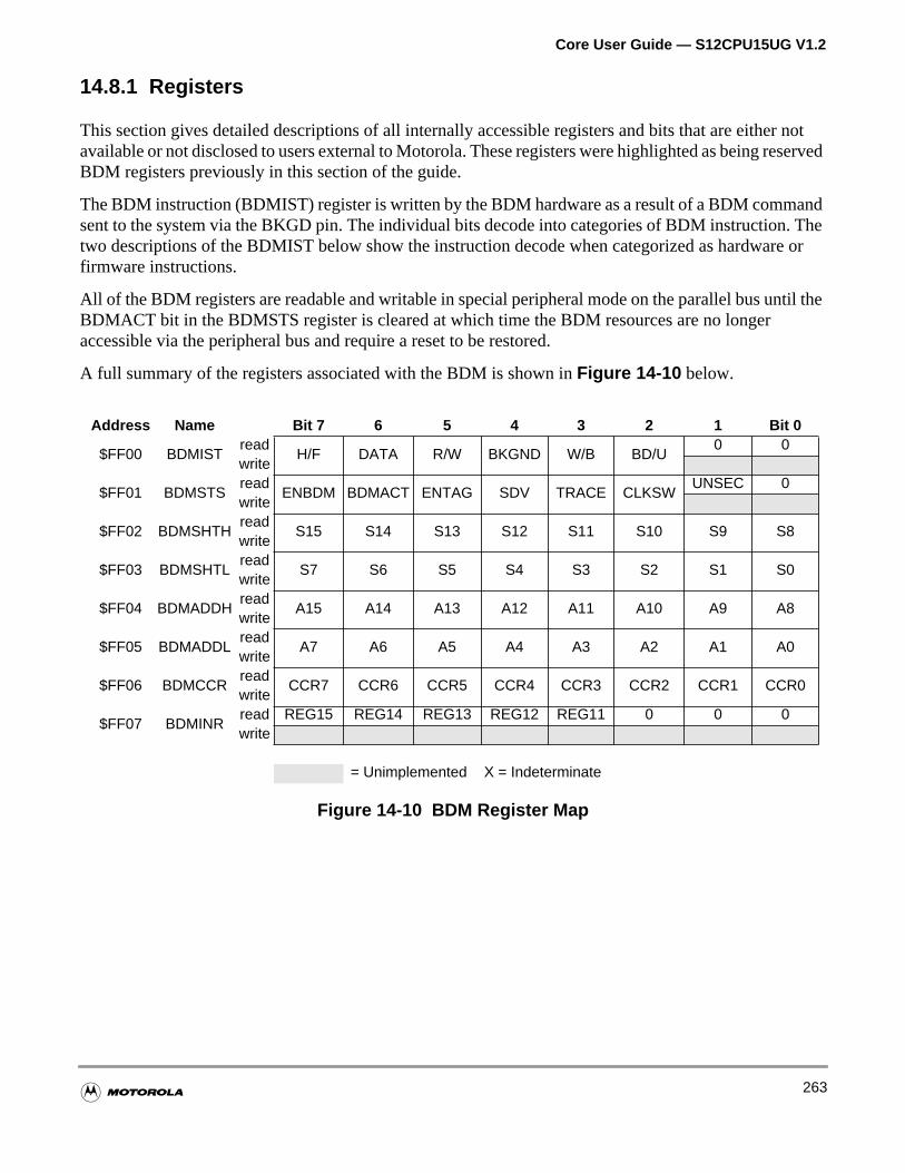
Core User Guide — S12CPU15UG V1.2
r notserved
ndThee or
til the
14.8.1 Registers
This section gives detailed descriptions of all internally accessible registers and bits that are eitheavailable or not disclosed to users external to Motorola. These registers were highlighted as being reBDM registers previously in this section of the guide.
The BDM instruction (BDMIST) register is written by the BDM hardware as a result of a BDM commasent to the system via the BKGD pin. The individual bits decode into categories of BDM instruction.two descriptions of the BDMIST below show the instruction decode when categorized as hardwarfirmware instructions.
All of the BDM registers are readable and writable in special peripheral mode on the parallel bus unBDMACT bit in the BDMSTS register is cleared at which time the BDM resources are no longeraccessible via the peripheral bus and require a reset to be restored.
A full summary of the registers associated with the BDM is shown inFigure 14-10 below.
Figure 14-10 BDM Register Map
Address Name Bit 7 6 5 4 3 2 1 Bit 0
$FF00 BDMISTread
H/F DATA R/W BKGND W/B BD/U0 0
write
$FF01 BDMSTSread
ENBDM BDMACT ENTAG SDV TRACE CLKSWUNSEC 0
write
$FF02 BDMSHTHread
S15 S14 S13 S12 S11 S10 S9 S8write
$FF03 BDMSHTLread
S7 S6 S5 S4 S3 S2 S1 S0write
$FF04 BDMADDHread
A15 A14 A13 A12 A11 A10 A9 A8write
$FF05 BDMADDLread
A7 A6 A5 A4 A3 A2 A1 A0write
$FF06 BDMCCRread
CCR7 CCR6 CCR5 CCR4 CCR3 CCR2 CCR1 CCR0write
$FF07 BDMINRread REG15 REG14 REG13 REG12 REG11 0 0 0write
= Unimplemented X = Indeterminate
263
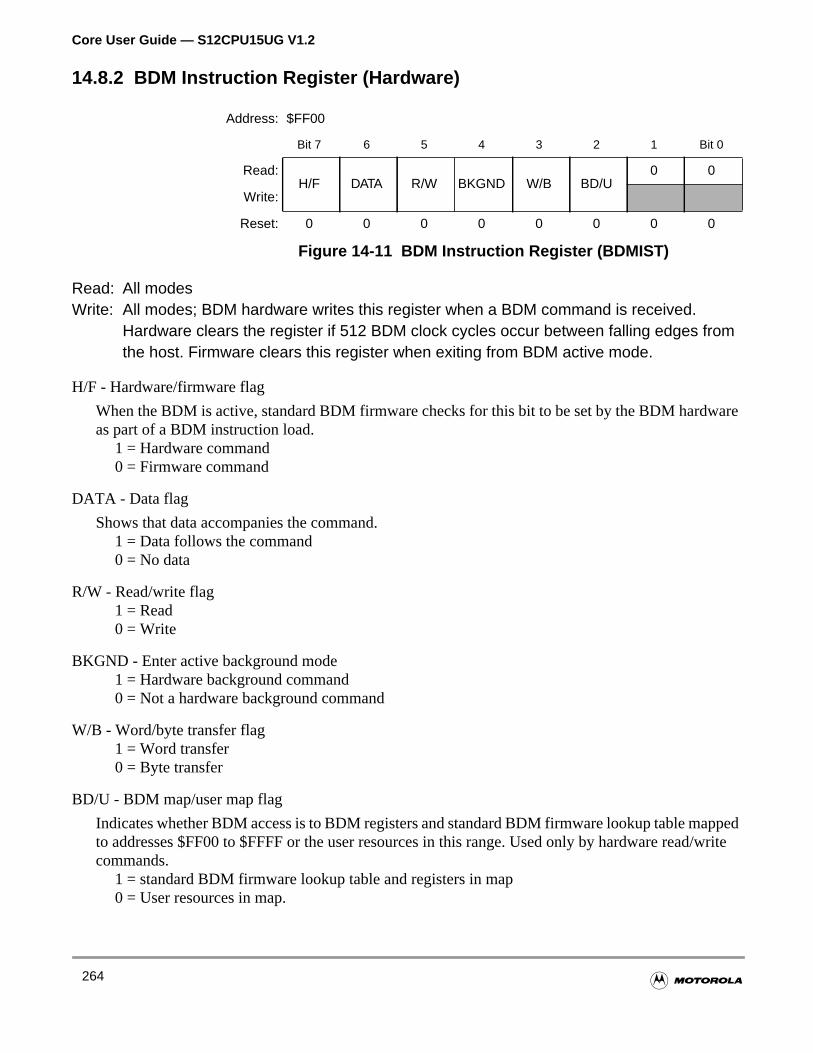
Core User Guide — S12CPU15UG V1.2
are
pped/write
14.8.2 BDM Instruction Register (Hardware)
Read: All modesWrite: All modes; BDM hardware writes this register when a BDM command is received.
Hardware clears the register if 512 BDM clock cycles occur between falling edges fromthe host. Firmware clears this register when exiting from BDM active mode.
H/F - Hardware/firmware flag
When the BDM is active, standard BDM firmware checks for this bit to be set by the BDM hardwas part of a BDM instruction load.
1 = Hardware command0 = Firmware command
DATA - Data flag
Shows that data accompanies the command.1 = Data follows the command0 = No data
R/W - Read/write flag1 = Read0 = Write
BKGND - Enter active background mode1 = Hardware background command0 = Not a hardware background command
W/B - Word/byte transfer flag1 = Word transfer0 = Byte transfer
BD/U - BDM map/user map flag
Indicates whether BDM access is to BDM registers and standard BDM firmware lookup table mato addresses $FF00 to $FFFF or the user resources in this range. Used only by hardware readcommands.
1 = standard BDM firmware lookup table and registers in map0 = User resources in map.
Address: $FF00
Bit 7 6 5 4 3 2 1 Bit 0
Read:H/F DATA R/W BKGND W/B BD/U
0 0
Write:
Reset: 0 0 0 0 0 0 0 0
Figure 14-11 BDM Instruction Register (BDMIST)
264
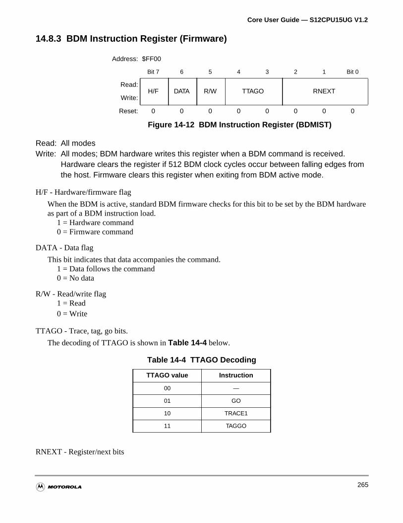
Core User Guide — S12CPU15UG V1.2
are
14.8.3 BDM Instruction Register (Firmware)
Read: All modesWrite: All modes; BDM hardware writes this register when a BDM command is received.
Hardware clears the register if 512 BDM clock cycles occur between falling edges fromthe host. Firmware clears this register when exiting from BDM active mode.
H/F - Hardware/firmware flag
When the BDM is active, standard BDM firmware checks for this bit to be set by the BDM hardwas part of a BDM instruction load.
1 = Hardware command0 = Firmware command
DATA - Data flag
This bit indicates that data accompanies the command.1 = Data follows the command0 = No data
R/W - Read/write flag1 = Read0 = Write
TTAGO - Trace, tag, go bits.
The decoding of TTAGO is shown inTable 14-4 below.
RNEXT - Register/next bits
Address: $FF00
Bit 7 6 5 4 3 2 1 Bit 0
Read:H/F DATA R/W TTAGO RNEXT
Write:
Reset: 0 0 0 0 0 0 0 0
Figure 14-12 BDM Instruction Register (BDMIST)
Table 14-4 TTAGO Decoding
TTAGO value Instruction
00 —
01 GO
10 TRACE1
11 TAGGO
265
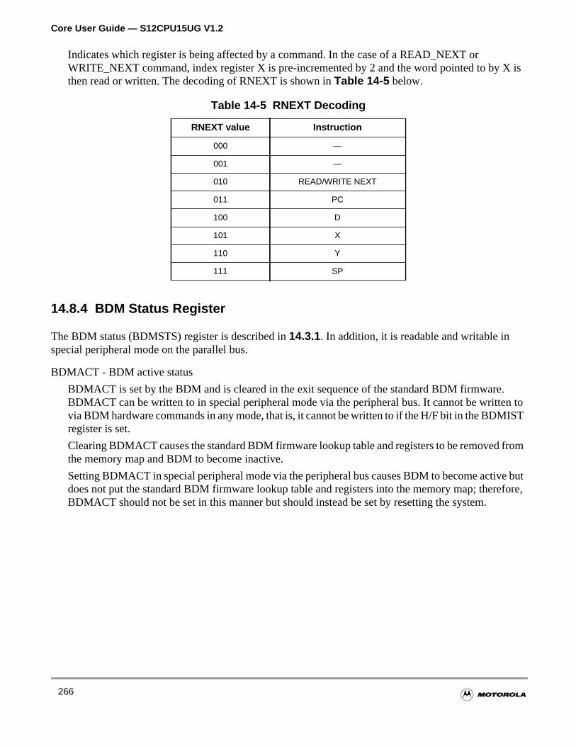
Core User Guide — S12CPU15UG V1.2
X is
.n toIST
from
e butrefore,
Indicates which register is being affected by a command. In the case of a READ_NEXT orWRITE_NEXT command, index register X is pre-incremented by 2 and the word pointed to bythen read or written. The decoding of RNEXT is shown inTable 14-5 below.
14.8.4 BDM Status Register
The BDM status (BDMSTS) register is described in14.3.1. In addition, it is readable and writable inspecial peripheral mode on the parallel bus.
BDMACT - BDM active status
BDMACT is set by the BDM and is cleared in the exit sequence of the standard BDM firmwareBDMACT can be written to in special peripheral mode via the peripheral bus. It cannot be writtevia BDM hardware commands in any mode, that is, it cannot be written to if the H/F bit in the BDMregister is set.
Clearing BDMACT causes the standard BDM firmware lookup table and registers to be removedthe memory map and BDM to become inactive.
Setting BDMACT in special peripheral mode via the peripheral bus causes BDM to become activdoes not put the standard BDM firmware lookup table and registers into the memory map; theBDMACT should not be set in this manner but should instead be set by resetting the system.
Table 14-5 RNEXT Decoding
RNEXT value Instruction
000 —
001 —
010 READ/WRITE NEXT
011 PC
100 D
101 X
110 Y
111 SP
266
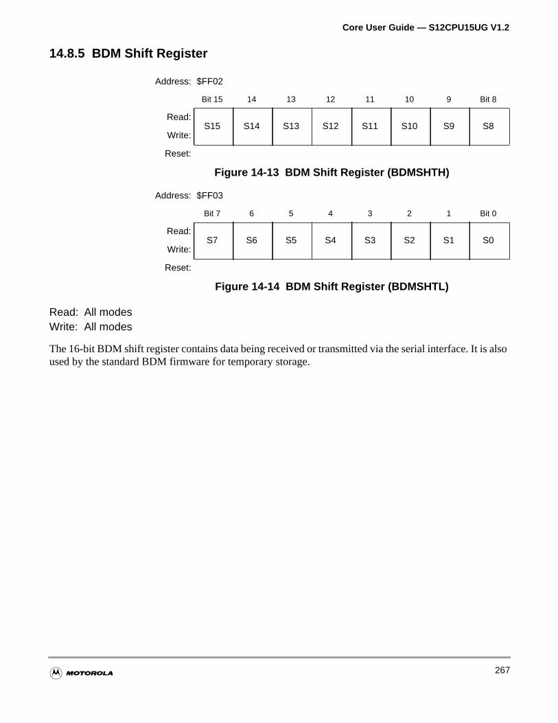
Core User Guide — S12CPU15UG V1.2
also
14.8.5 BDM Shift Register
Read: All modesWrite: All modes
The 16-bit BDM shift register contains data being received or transmitted via the serial interface. It isused by the standard BDM firmware for temporary storage.
Address: $FF02
Bit 15 14 13 12 11 10 9 Bit 8
Read:S15 S14 S13 S12 S11 S10 S9 S8
Write:
Reset:
Figure 14-13 BDM Shift Register (BDMSHTH)
Address: $FF03
Bit 7 6 5 4 3 2 1 Bit 0
Read:S7 S6 S5 S4 S3 S2 S1 S0
Write:
Reset:
Figure 14-14 BDM Shift Register (BDMSHTL)
267
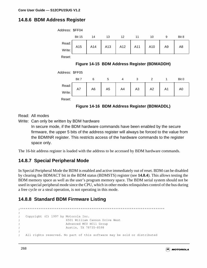
Core User Guide — S12CPU15UG V1.2
ds.
abled
not beduring
14.8.6 BDM Address Register
Read: All modesWrite: Can only be written by BDM hardware
In secure mode, if the BDM hardware commands have been enabled by the securefirmware, the upper 5 bits of the address register will always be forced to the value fromthe BDMINR register. This restricts access of the hardware commands to the registerspace only.
The 16-bit address register is loaded with the address to be accessed by BDM hardware comman
14.8.7 Special Peripheral Mode
In Special Peripheral Mode the BDM is enabled and active immediately out of reset. BDM can be disby clearing the BDMACT bit in the BDM status (BDMSTS) register (see14.8.4). This allows testing theBDM memory space as well as the user’s program memory space. The BDM serial system shouldused in special peripheral mode since the CPU, which in other modes relinquishes control of the busa free cycle or a steal operation, is not operating in this mode.
14.8.8 Standard BDM Firmware Listing
;*******************************************************************************;; Copyright (C) 1997 by Motorola Inc.; 6501 William Cannon Drive West; Advanced MCU HC11 Group; Austin, TX 78735-8598;; All rights reserved. No part of this software may be sold or distributed
Address: $FF04
Bit 15 14 13 12 11 10 9 Bit 8
Read:A15 A14 A13 A12 A11 A10 A9 A8
Write:
Reset:
Figure 14-15 BDM Address Register (BDMADDH)
Address: $FF05
Bit 7 6 5 4 3 2 1 Bit 0
Read:A7 A6 A5 A4 A3 A2 A1 A0
Write:
Reset:
Figure 14-16 BDM Address Register (BDMADDL)
268
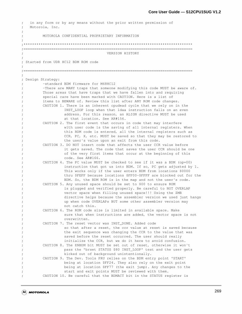
Core User Guide — S12CPU15UG V1.2
; in any form or by any means without the prior written permission of; Motorola, Inc.;; MOTOROLA CONFIDENTIAL PROPRIETARY INFORMATION;;*******************************************************************************;===============================================================================; VERSION HISTORY;; Started from UDR HC12 BDM ROM code;;===============================================================================;; Design Strategy:; -standard BDM firmware for M68HC12; -There are MANY traps that someone modifying this code MUST be aware of.; Those areas that have traps that we have fallen into and requiring; special care have been marked with CAUTION. Here is a list of; items to BEWARE of. Review this list after ANY ROM code changes.; CAUTION 1. There is an inherent cpudead cycle that we rely on in the; INST_LOOP loop when that ldaa instruction falls on an even; address. For this reason, an ALIGN directive MUST be used; at that location. See AR#156.; CAUTION 2. The first event that occurs in code that may interfere; with user code is the saving of all internal registers. When; this BDM code is entered, all the internal registers such as; CCR, PC, X, etc. MUST be saved so that they may be restored to; the user's value upon an exit from this code.; CAUTION 3. DO NOT insert code that affects the user CCR value before; it gets saved. The code that saves the user CCR should be one; of the very first items that occur at the beginning of this; code. See AR#166.; CAUTION 4. The PC value MUST be checked to see if it was a BDM (op=00); instruction that got us into BDM. If so, PC gets adjusted by 1.; This works only if the user enters BDM from locations $0000; thru $FEFF because locations $FF00-$FFFF are blocked out for the; BDM. So, the BDM ROM is in the map and not the user's code.; CAUTION 5. Any unused space should be set to $00 to ensure ROM; is plugged and verified properly. Be careful to NOT OVERLAP; vector space when filling unused space!!! Using the ZMB; directive helps because the assembler version we used just hangs; up when code OVERLAPs BUT some other assembler version may; not catch this.; CAUTION 6. The ROM code size is limited in available space. Make; sure that when instructions are added, the vector space is not; overwritten.; CAUTION 7. The reset vector was INST_DONE. Added code; so that after a reset, the ccr value at reset is saved because; the exit sequence was changing the CCR to the value that was; saved before the reset occurred. The user should really; initialize the CCR, but we do it here to avoid confusion.; CAUTION 8. The ENBDM bit MUST be set out of reset, otherwise it won't; pass the "brset STATUS $80 INST_LOOP" test and the user gets; kicked out of background unintentionally.; CAUTION 9. The Dev. Tools PRU relies on the BDM entry point "START"; being at location $FF24. They also rely on the exit point; being at location $FF77 (the exit jump). Any changes to the; start and exit points MUST be reviewed with them.; CAUTION 10. Be careful that the BDMACT bit in the STATUS register is
269
Core User Guide — S12CPU15UG V1.2
; not unintentionally changed from a 1 to a 0 during 16-bit; manipulation of the INSTRUCTION register. This will cause a; race condition because BDMACT=0 will disable the standard BDM firmware; ROM while the CPU is executing this firmware.; -This is a list of instructions which use the temp2 (t2) and temp3 (t3); instructions. List as of 7-27-94. Gotten from Tom Poterek's BDMcode.; temp2; =====; bgnd; emacs; etbl; mem; revw; stop; tbl; wai; execution of BDM ROM;; temp3; =====; emacs; etbl; mem; puld; pulx; puly; rtc; rti; rts; tbl; wav; execution of BDM ROM;
********************************************************************************
********************************************************************************* EQUATES
fff6 BDMVEC equ$fff6 ;First BDM ROM vector.
ff00 org$ff00 ;Start of BDM map (registers)ff00 INSTR rmb1 ;Instruction (command) register
* s/w ! H/S ! DATA ! R/W ! TTAG : GO ! R2 ! R1 ! R0 !* hdw ! H/S ! DATA ! R/W !BKGND : W/B !BD/USR! NEXT ! - !* Reg codes: R2:R1:R0* 0:0:0 - Illegal, command $00 is null command* 0:0:1 - not used* 0:1:0 - Next Word 2,+X pre inc X by 2 and r/w next word (,X)* later r/w next will work from ADDRESS reg value not X* 0:1:1 - PC* 1:0:0 - D* 1:0:1 - X* 1:1:0 - Y* 1:1:1 - SP* TTAG:GO coding:* 0:0 - No execution command* 0:1 - Go to user program* 1:0 - Trace one user instruction and return to BDM
270
Core User Guide — S12CPU15UG V1.2
* 1:1 - Tag Go command (reconfigure BKGD pin for tagging in)
ff01 STATUS rmb1 ;Status/Control register* ! enBDM!BDACTV! TAG ! VALID: TRACE! - ! - ! - !* Exit conditions vs value written to STATUS on exit* BDM not allowed - $00* Trace 1 - $88* Go - $80* Tag Go - $A0
ff02 SHIFTER rmb2 ;For serial data in/out
ff04 ADDRESS rmb2 ;Address for some commands* ADDRESS will be read-only on first parts but later it will* be r/w so r/w next word doesn't need to use X
ff06 CCRSAVE rmb1 ;Save user CCR value while in BDM* CCRSAVE also used briefly to hold exit value for status* during exit sequence to return to user code
ff20 orgff20 ;BDM ROM startAFTER_RST ;*****CAUTION 7. *****CAUTION 8.
ff20 1c ff 01 80 bset STATUS $80;Set the ENBDM bit to pass the brset;test below.;CCR immediately after rst is;SXHINZVC=11x1xxxx.;CCR after this bset is;SXHINZVC=11x1100x. This is o.k.;because the SXI bits are not;affected.
START;*****CAUTION 2. *****CAUTION 9.
ff24 b7 b4 exgt3 d ;Save D without affecting CCR.;This "exg t3 d" instruction MUST;occur before the following;"tfr ccr a" instruction.
;*****CAUTION 3.ff26 b7 20 tfrccr aff28 7a ff 06 staaCCRSAVE;Save user CCR valueff2b b7 d3 exgx t2 ;pc into x. *****CAUTION 4.ff2d 8e ff 00 cpx#$FF00 ;Check to see if user PC overlaps BDM
;ROM.ff30 24 04 bhsROM_INC;If so, increment regardless.ff32 e7 00 tst0,x ;Test next opcode. This instruction
;affects CCR so it MUST occur AFTER;saving the user's CCR.
ff34 26 01 bneRES_X_T2;if not $00, restoreff36 08 ROM_INC inx ;else inc, then restore. This
;instruction affects CCR so it MUST;occur AFTER saving the user's CCR.
RES_X_T2ff37 b7 d3 exgx t2 ;restore pc to temp 2ff39 1e ff 01 80 06 brsetSTATUS $80 INST_LOOP ;Check if BDM allowedff3e 87 clra ;Exit if BDM not allowedff3f 20 1c braEXIT_SEQ
* Above is 1 of 4 ways to exit BDM to user code.INST_DONE
ff41 79 ff 00 clrINSTR ;clear INSTR then wait for new inst
271
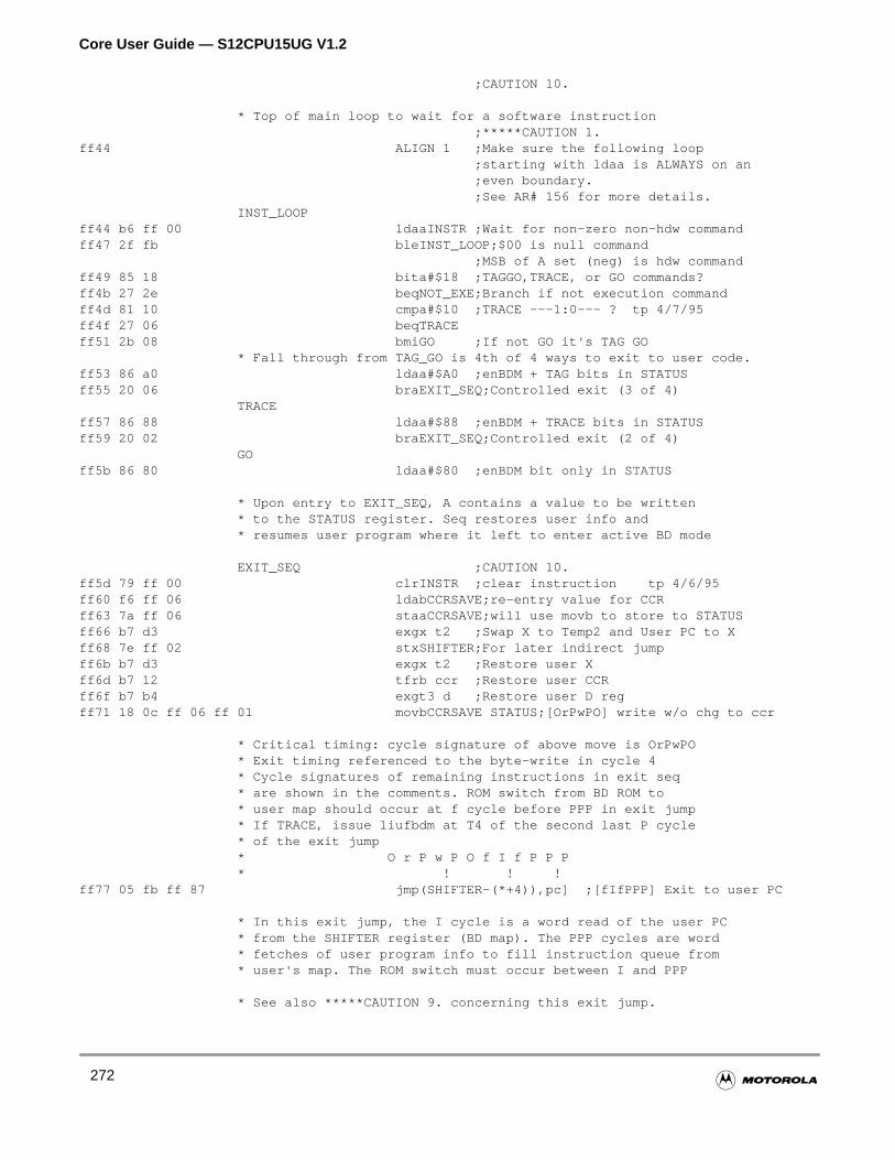
Core User Guide — S12CPU15UG V1.2
;CAUTION 10.
* Top of main loop to wait for a software instruction;*****CAUTION 1.
ff44 ALIGN 1 ;Make sure the following loop;starting with ldaa is ALWAYS on an;even boundary.;See AR# 156 for more details.
INST_LOOPff44 b6 ff 00 ldaaINSTR ;Wait for non-zero non-hdw commandff47 2f fb bleINST_LOOP;$00 is null command
;MSB of A set (neg) is hdw commandff49 85 18 bita#$18 ;TAGGO,TRACE, or GO commands?ff4b 27 2e beqNOT_EXE;Branch if not execution commandff4d 81 10 cmpa#$10 ;TRACE ---1:0--- ? tp 4/7/95ff4f 27 06 beqTRACEff51 2b 08 bmiGO ;If not GO it's TAG GO
* Fall through from TAG_GO is 4th of 4 ways to exit to user code.ff53 86 a0 ldaa#$A0 ;enBDM + TAG bits in STATUSff55 20 06 braEXIT_SEQ;Controlled exit (3 of 4)
TRACEff57 86 88 ldaa#$88 ;enBDM + TRACE bits in STATUSff59 20 02 braEXIT_SEQ;Controlled exit (2 of 4)
GOff5b 86 80 ldaa#$80 ;enBDM bit only in STATUS
* Upon entry to EXIT_SEQ, A contains a value to be written* to the STATUS register. Seq restores user info and* resumes user program where it left to enter active BD mode
EXIT_SEQ ;CAUTION 10.ff5d 79 ff 00 clrINSTR ;clear instruction tp 4/6/95ff60 f6 ff 06 ldabCCRSAVE;re-entry value for CCRff63 7a ff 06 staaCCRSAVE;will use movb to store to STATUSff66 b7 d3 exgx t2 ;Swap X to Temp2 and User PC to Xff68 7e ff 02 stxSHIFTER;For later indirect jumpff6b b7 d3 exgx t2 ;Restore user Xff6d b7 12 tfrb ccr ;Restore user CCRff6f b7 b4 exgt3 d ;Restore user D regff71 18 0c ff 06 ff 01 movbCCRSAVE STATUS;[OrPwPO] write w/o chg to ccr
* Critical timing: cycle signature of above move is OrPwPO* Exit timing referenced to the byte-write in cycle 4* Cycle signatures of remaining instructions in exit seq* are shown in the comments. ROM switch from BD ROM to* user map should occur at f cycle before PPP in exit jump* If TRACE, issue liufbdm at T4 of the second last P cycle* of the exit jump* O r P w P O f I f P P P* ! ! !
ff77 05 fb ff 87 jmp(SHIFTER-(*+4)),pc] ;[fIfPPP] Exit to user PC
* In this exit jump, the I cycle is a word read of the user PC* from the SHIFTER register (BD map). The PPP cycles are word* fetches of user program info to fill instruction queue from* user's map. The ROM switch must occur between I and PPP
* See also *****CAUTION 9. concerning this exit jump.
272

Core User Guide — S12CPU15UG V1.2
NOT_EXEff7b b7 01 tfra b ;Duplicate command in Bff7d 84 07 anda#$07 ;Strip all but 3-bit reg codeff7f 80 02 suba#2 ;codes 0 & 1 illegal or unusedff81 2b be bmiINST_DONE;branch if A now negativeff83 c5 20 bitb#$20 ;Check R/W bitff85 26 37 bne;COMP_GOTO;Go decode read command (was beq
;tp 3/30)
WAIT_DATAff87 f7 ff 00 tstINSTR ;Check for new commandff8a 27 b8 beqINST_LOOP;Need escape if old command abortedff8c 1f ff 01 10 f6 brclrSTATUS $10 WAIT_DATA ;Wait for data readyff91 c6 07 ldab#7ff93 12 mul ;B = 7*(reg_code - 1)ff94 05 fd jmpb,pc ;Calculated GOTO
* Each write command corresponding to reg code 2-7 takes* exactly 7 bytes. For command 2 (write next word) the jump will* GOTO 0,pc or the location immediately after the jump* For command 7 (write SP) the jump will go to (5*7),pc* Each command ends with a branch to the main command loopW_NXT_WRD
ff96 fc ff 02 lddSHIFTER;Get data to writeff99 6c 21 std2,+x ;pre-inc x by 2 and store word
INST_DONE1ff9b 20 a4 braINST_DONE;Intermediate branch to loop top
WRITE_PCff9d fc ff 02 lddSHIFTER;Get data to writeffa0 b7 c3 exgd t2 ;User PC in Temp2 regffa2 20 9d braINST_DONE;Branch to loop top
WRITE_Dffa4 fc ff 02 lddSHIFTER;Get data to writeffa7 b7 b4 exgt3 d ;User D in Temp3 reg (was exg d t2
;tp 3/28)ffa9 20 96 braINST_DONE;Branch to loop top
WRITE_Xffab fe ff 02 ldxSHIFTER;Update X registerffae 20 91 braINST_DONE;Branch to loop topffb0 a7 nop ;Pad to make command take 7 bytesffb1 a7 nop
WRITE_Yffb2 fd ff 02 ldySHIFTER;Update Y registerffb5 20 8a braINST_DONE;Branch to loop topffb7 a7 nop ;Pad to make command take 7 bytesffb8 a7 nop
WRITE_SPffb9 ff ff 02 ldsSHIFTER;Update SP registerffbc 20 83 braINST_DONE;Branch to loop top
* No need to pad last command since we don't index past it.
COMP_GOTOffbe 48 asla ;x2ffbf 48 asla ;A = (reg_code - 2)*4ffc0 05 fc jmpa,pc ;Calculated GOTO
273
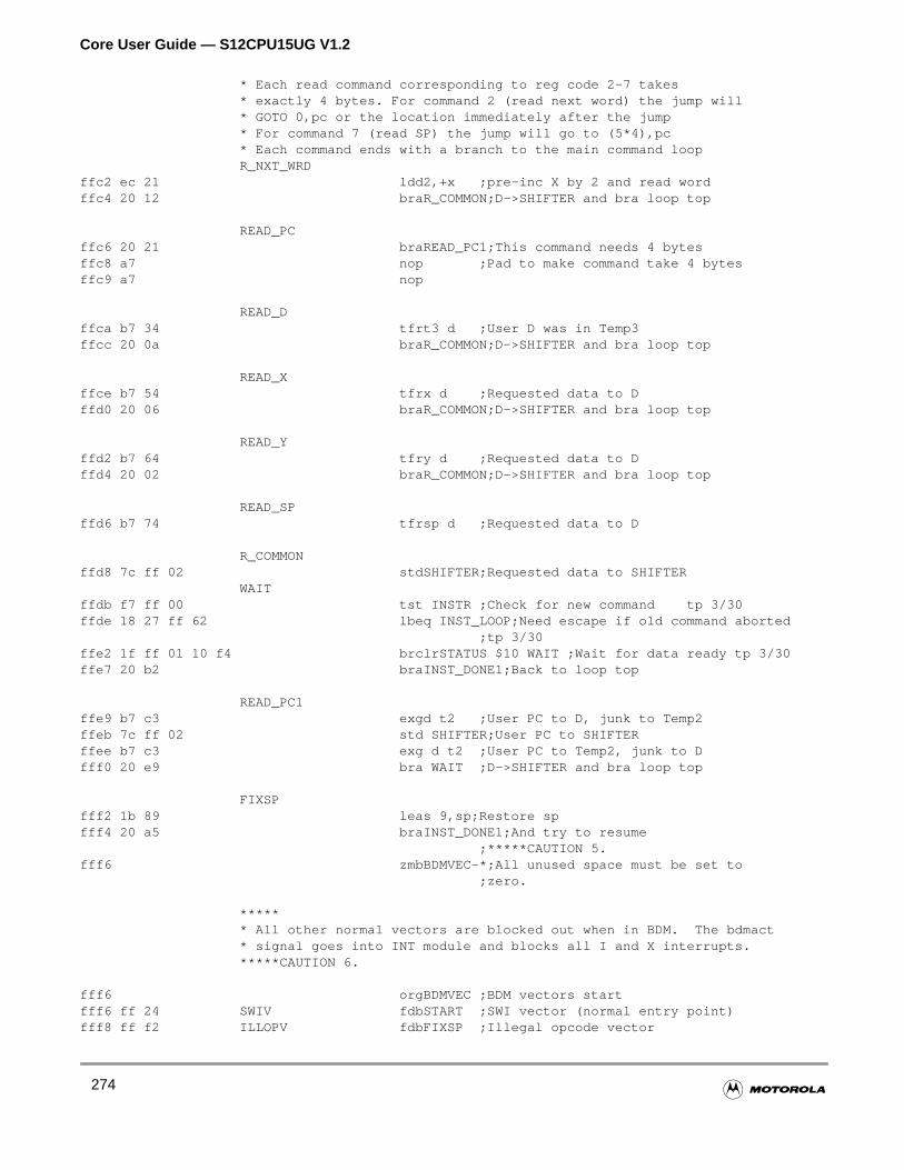
Core User Guide — S12CPU15UG V1.2
* Each read command corresponding to reg code 2-7 takes* exactly 4 bytes. For command 2 (read next word) the jump will* GOTO 0,pc or the location immediately after the jump* For command 7 (read SP) the jump will go to (5*4),pc* Each command ends with a branch to the main command loopR_NXT_WRD
ffc2 ec 21 ldd2,+x ;pre-inc X by 2 and read wordffc4 20 12 braR_COMMON;D->SHIFTER and bra loop top
READ_PCffc6 20 21 braREAD_PC1;This command needs 4 bytesffc8 a7 nop ;Pad to make command take 4 bytesffc9 a7 nop
READ_Dffca b7 34 tfrt3 d ;User D was in Temp3ffcc 20 0a braR_COMMON;D->SHIFTER and bra loop top
READ_Xffce b7 54 tfrx d ;Requested data to Dffd0 20 06 braR_COMMON;D->SHIFTER and bra loop top
READ_Yffd2 b7 64 tfry d ;Requested data to Dffd4 20 02 braR_COMMON;D->SHIFTER and bra loop top
READ_SPffd6 b7 74 tfrsp d ;Requested data to D
R_COMMONffd8 7c ff 02 stdSHIFTER;Requested data to SHIFTER
WAITffdb f7 ff 00 tst INSTR ;Check for new command tp 3/30ffde 18 27 ff 62 lbeq INST_LOOP;Need escape if old command aborted
;tp 3/30ffe2 1f ff 01 10 f4 brclrSTATUS $10 WAIT ;Wait for data ready tp 3/30ffe7 20 b2 braINST_DONE1;Back to loop top
READ_PC1ffe9 b7 c3 exgd t2 ;User PC to D, junk to Temp2ffeb 7c ff 02 std SHIFTER;User PC to SHIFTERffee b7 c3 exg d t2 ;User PC to Temp2, junk to Dfff0 20 e9 bra WAIT ;D->SHIFTER and bra loop top
FIXSPfff2 1b 89 leas 9,sp;Restore spfff4 20 a5 braINST_DONE1;And try to resume
;*****CAUTION 5.fff6 zmbBDMVEC-*;All unused space must be set to
;zero.
****** All other normal vectors are blocked out when in BDM. The bdmact* signal goes into INT module and blocks all I and X interrupts.*****CAUTION 6.
fff6 orgBDMVEC ;BDM vectors startfff6 ff 24 SWIV fdbSTART ;SWI vector (normal entry point)fff8 ff f2 ILLOPV fdbFIXSP ;Illegal opcode vector
274
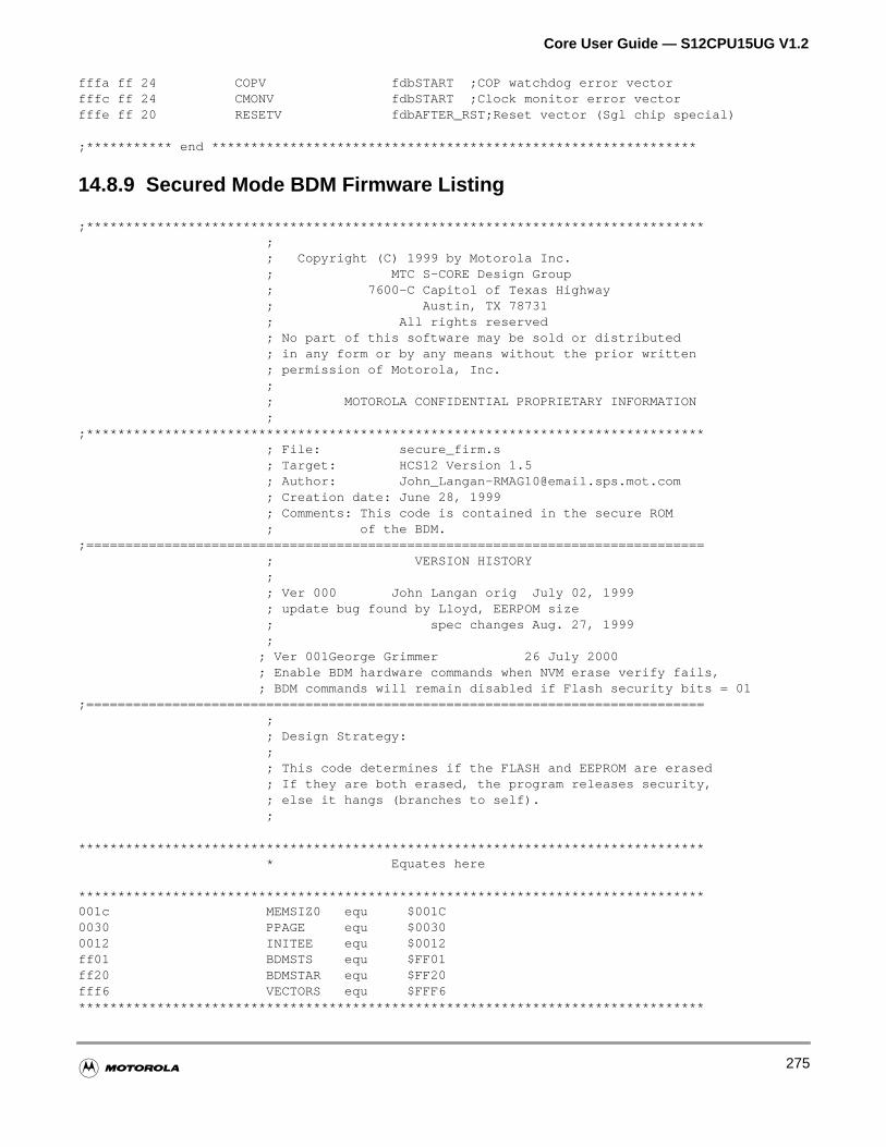
Core User Guide — S12CPU15UG V1.2
fffa ff 24 COPV fdbSTART ;COP watchdog error vectorfffc ff 24 CMONV fdbSTART ;Clock monitor error vectorfffe ff 20 RESETV fdbAFTER_RST;Reset vector (Sgl chip special)
;*********** end **************************************************************
14.8.9 Secured Mode BDM Firmware Listing
;******************************************************************************* ; ; Copyright (C) 1999 by Motorola Inc. ; MTC S-CORE Design Group ; 7600-C Capitol of Texas Highway ; Austin, TX 78731 ; All rights reserved ; No part of this software may be sold or distributed ; in any form or by any means without the prior written ; permission of Motorola, Inc. ; ; MOTOROLA CONFIDENTIAL PROPRIETARY INFORMATION ;;******************************************************************************* ; File: secure_firm.s ; Target: HCS12 Version 1.5 ; Author: [email protected] ; Creation date: June 28, 1999 ; Comments: This code is contained in the secure ROM ; of the BDM.;=============================================================================== ; VERSION HISTORY ; ; Ver 000 John Langan orig July 02, 1999 ; update bug found by Lloyd, EERPOM size ; spec changes Aug. 27, 1999 ; ; Ver 001George Grimmer 26 July 2000 ; Enable BDM hardware commands when NVM erase verify fails, ; BDM commands will remain disabled if Flash security bits = 01;=============================================================================== ; ; Design Strategy: ; ; This code determines if the FLASH and EEPROM are erased ; If they are both erased, the program releases security, ; else it hangs (branches to self). ;
******************************************************************************** * Equates here
********************************************************************************001c MEMSIZ0 equ $001C0030 PPAGE equ $00300012 INITEE equ $0012ff01 BDMSTS equ $FF01ff20 BDMSTAR equ $FF20fff6 VECTORS equ $FFF6********************************************************************************
275
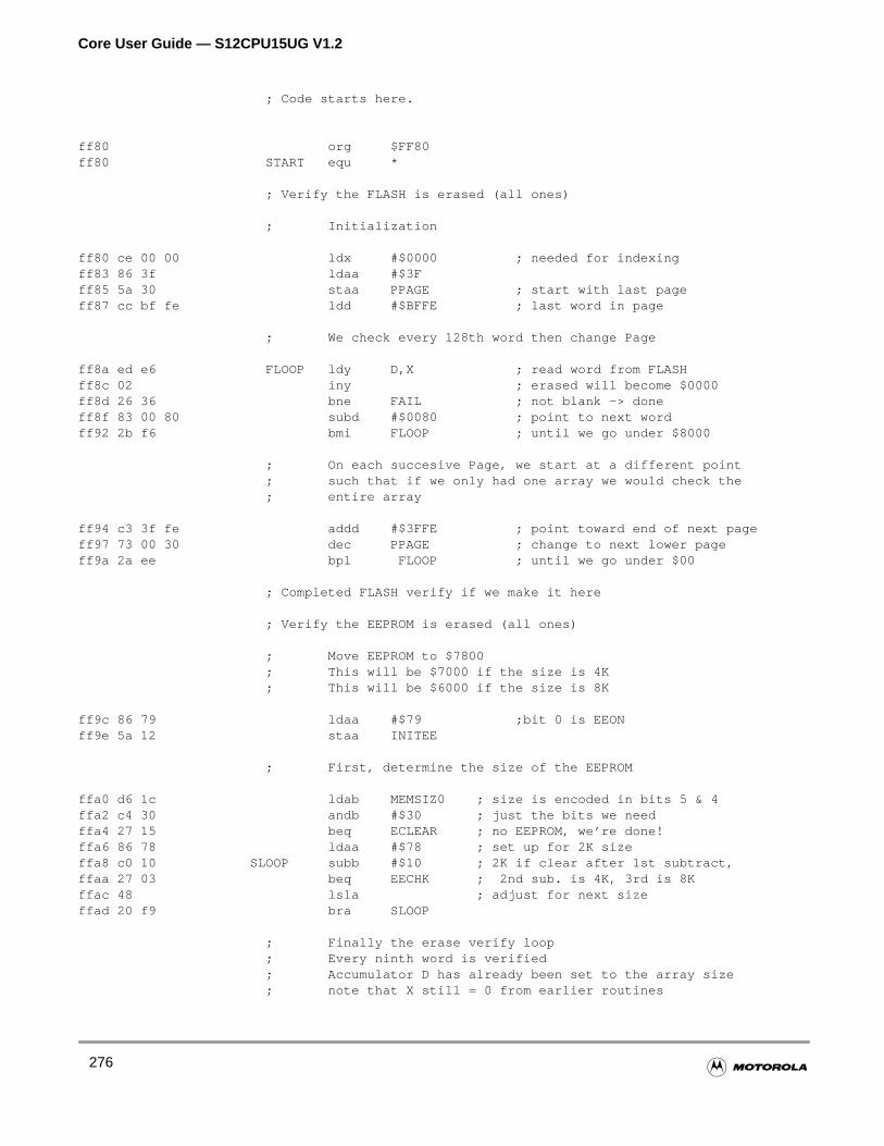
Core User Guide — S12CPU15UG V1.2
; Code starts here.
ff80 org $FF80ff80 START equ *
; Verify the FLASH is erased (all ones)
; Initialization
ff80 ce 00 00 ldx #$0000 ; needed for indexingff83 86 3f ldaa #$3Fff85 5a 30 staa PPAGE ; start with last pageff87 cc bf fe ldd #$BFFE ; last word in page
; We check every 128th word then change Page
ff8a ed e6 FLOOP ldy D,X ; read word from FLASHff8c 02 iny ; erased will become $0000ff8d 26 36 bne FAIL ; not blank -> doneff8f 83 00 80 subd #$0080 ; point to next wordff92 2b f6 bmi FLOOP ; until we go under $8000
; On each succesive Page, we start at a different point ; such that if we only had one array we would check the ; entire array
ff94 c3 3f fe addd #$3FFE ; point toward end of next pageff97 73 00 30 dec PPAGE ; change to next lower pageff9a 2a ee bpl FLOOP ; until we go under $00
; Completed FLASH verify if we make it here
; Verify the EEPROM is erased (all ones)
; Move EEPROM to $7800 ; This will be $7000 if the size is 4K ; This will be $6000 if the size is 8K
ff9c 86 79 ldaa #$79 ;bit 0 is EEONff9e 5a 12 staa INITEE
; First, determine the size of the EEPROM
ffa0 d6 1c ldab MEMSIZ0 ; size is encoded in bits 5 & 4ffa2 c4 30 andb #$30 ; just the bits we needffa4 27 15 beq ECLEAR ; no EEPROM, we’re done!ffa6 86 78 ldaa #$78 ; set up for 2K sizeffa8 c0 10 SLOOP subb #$10 ; 2K if clear after 1st subtract,ffaa 27 03 beq EECHK ; 2nd sub. is 4K, 3rd is 8Kffac 48 lsla ; adjust for next sizeffad 20 f9 bra SLOOP
; Finally the erase verify loop ; Every ninth word is verified ; Accumulator D has already been set to the array size ; note that X still = 0 from earlier routines
276
Core User Guide — S12CPU15UG V1.2
ffaf 84 78 EECHK anda #$78 ; index D + X = last wordffb1 ed e6 ELOOP ldy D,X ; read word from EEPROMffb3 02 iny ; erased will become $0000ffb4 26 0f bne FAIL ; not blank -> doneffb6 c3 00 12 addd #$0012 ; point to next wordffb9 2a f6 bpl ELOOP ; until we get to or under $4000
; When we arrive here, all is clear
ffbb 86 42 ECLEAR ldaa #$42 ; bit #1 is UNSECffbd ce ff 01 ldx #BDMSTSffc0 6a 00 staa 0,X ; use instr that ends with write cycleffc2 06 ff 20 jmp BDMSTAR
; Failures arrive here, forever.....
ffc5 18 0b 3f 00 30 FAIL movb #$3f,PPAGEffca f6 bf 0f ldab $BF0Fffcd ca fc orab #$FCffcf ce ff 01 ldx #BDMSTSffd2 86 80 ldaa #$80ffd4 aa 00 oraa 0,xffd6 53 decbffd7 27 03 beq BDMLOCKffd9 6a 00 staa 0,xffdb a7 align 1 BDMLOCKffdc a7 nopffdd 20 fd bra BDMLOCK
; Clear out space between here and the vectors
ffdf 00 00 00 00 00 00 zmb VECTORS-* 00 00 00 00 00 00 00 00 00 00 00 00 00 00 00 00 00
; VECTORS HEREfff6 org VECTORSfff6 ff 24 fdb BDMSTAR+4 ; SWIfff8 ff c5 fdb FAIL ; TRAPfffa ff 80 fdb START ; COPfffc ff 80 fdb START ; CLK Monitorfffe ff 80 fdb START ; RESET
;*********** end **************************************************************
277

Core User Guide — S12CPU15UG V1.2
278
Core User Guide — S12CPU15UG V1.2
nts ofode or allstemgured
Section 15 Secured Mode of Operation
This section provides a brief description of the secured mode of operation of the Core. Detailedinformation relating to integration issues is provided in theHCS12 V1.5 Core Integration Guide.
15.1 Overview
The implementation of the secured mode of operation for the Core provides for protecting the conteinternal (on-chip) memory arrays. While in secured mode the system can execute in single-chip mfrom an external memory block but the contents of the internal memory will not be accessible andnormal BDM functions will be blocked from execution. A mechanism is provided to release the syfrom the secured mode at which time normal operation will resume allowing the system to be reconfifor unsecured mode.
15.1.1 Features
The secured mode of operation provides:
• Protection of internal (on-chip) Flash EEPROM contents
• Protection of internal (on-chip) EEPROM contents
• Operation in single-chip mode while secured
• Operation from external memory with internal Flash and EEPROM disabled while secured
279
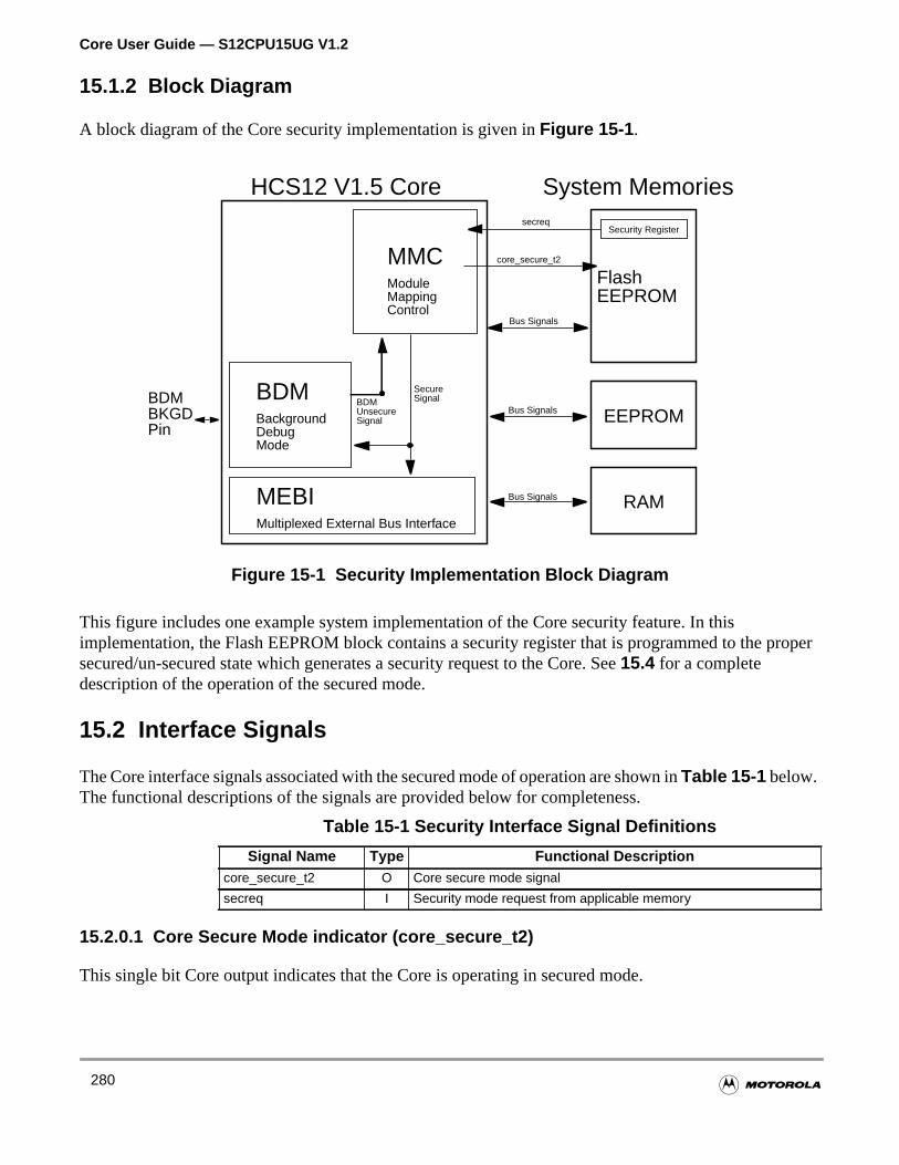
Core User Guide — S12CPU15UG V1.2
proper
15.1.2 Block Diagram
A block diagram of the Core security implementation is given inFigure 15-1 .
Figure 15-1 Security Implementation Block Diagram
This figure includes one example system implementation of the Core security feature. In thisimplementation, the Flash EEPROM block contains a security register that is programmed to the secured/un-secured state which generates a security request to the Core. See15.4 for a completedescription of the operation of the secured mode.
15.2 Interface Signals
The Core interface signals associated with the secured mode of operation are shown inTable 15-1 below.The functional descriptions of the signals are provided below for completeness.
15.2.0.1 Core Secure Mode indicator (core_secure_t2)
This single bit Core output indicates that the Core is operating in secured mode.
Table 15-1 Security Interface Signal Definitions
Signal Name Type Functional Descriptioncore_secure_t2 O Core secure mode signal
secreq I Security mode request from applicable memory
BDMBackgroundDebugMode
MMCModuleMappingControl
MEBIMultiplexed External Bus Interface
BDMBKGDPin
RAM
EEPROM
FlashEEPROM
Bus Signals
Bus Signals
Bus Signals
Security Register
HCS12 V1.5 Core
Secure
core_secure_t2
SignalBDMUnsecureSignal
secreq
System Memories
280
Core User Guide — S12CPU15UG V1.2
e Core
olatilelease
rmaled byell as a
ode.BDM
atile
rectlyPROMed.be
and
ass
and
the
15.2.0.2 Core Security Request (secreq)
This single bit input indicates to the Core that the system memory is in a secured state and that thshould operate in secured mode.
15.3 Registers
There are no registers in the Core associated with the secured mode of operation. Typically, a non-vmemory block in the system will contain a register for programming the state of system security. Prefer to the chip-level and/or memory block documentation for implementation details.
15.4 Operation
When the system is configured for secured mode of operation, it will normally operate in either nosingle-chip mode or in an expanded mode executing from external memory. The conditions impossecured mode for each of these operating modes is discussed in the subsections that follow as wdescription of the method to unsecure the system.
15.4.1 Normal Single-Chip Mode
Normal single-chip mode will be the most common operation of a system configured for secured mThe system functionality will appear just as an unsecured system with the exception imposed that theoperation will not be allowed and will be blocked. This will prevent any access to the internal non-volmemory block contents.
15.4.2 Expanded Mode
To operate in secured mode and execute from external memory space, the system should be corconfigured for secured mode and then reset into expanded mode. The internal (on-chip) Flash EEand EEPROM blocks (if applicable) will be disabled and unavailable. All BDM operation will be blockIn addition, while in secured mode all internal visibility (IVIS) and CPU pipe (IPIPE) information willblocked from output.
15.4.3 Unsecuring The System
To unsecure a system that is configured for secured mode, the internal (on-chip) Flash EEPROMEEPROM must be fully erased. This can be performed using one of the following methods:
1. Reset the microcontroller into SPECIAL TEST mode, execute a program which writes the MErase command sequence into the Flash and EEPROM Command registers.
2. Reset the microcontroller into SPECIAL SINGLE CHIP mode, delay while the erase test isperformed by the BDM secure ROM. Send BDM commands to write the Mass Erase commsequence into the Flash and EEPROM Command registers.
3. Reset the microcontroller into SPECIAL PERIPHERAL mode, using SPM commands write Mass Erase command sequence into the Flash and EEPROM Command registers.
281

Core User Guide — S12CPU15UG V1.2
r. ThisM by any
end aess.
de, the
d byeys,er. Ing thehewill be
In all modes the mass erase command sequence must have the following steps:a. Write FCLKDIV register to set the Flash clock for proper timing.b. Write $00 to FCNFG register to select Flash block 0.c. Write $10 to FTSTMOD register to set WRALL bit.
(with WRALL set, all of the following writes to banked Flash registers will affect all Flashblocks.)
d. Disable Flash protection by writing the FPROT register.e. Write any data to Flash memory space $C000-$FFFFf. Write Mass Erase command($41) to FCMD register.g. Clear CBIEF (bit 7) it FSTAT register.h. Write ECLKDIV register to set the EEPROM clock for proper timing.i. Disable protection in EEPROM by writing the EPROT register.j. Write any data to EEPROM memory space.k. Write Mass Erase command($41) to ECMD register.l. Clear CBIEF (bit 7) it ESTAT register.m. Wait until all CCIF flags are set to 1 again.
After all the CCIF flags are set to 1 again, the Flash and EEPROM have been erased. Reset themicrocontroller into SPECIAL SINGLE CHIP mode. The BDM secure ROM will verify that thenonvolatile memories are erased, and then it will assert the UNSEC bit in the BDM Status registewill cause the core_secure_t2 signal to de-assert, and the microcontroller will be unsecure. All BDcommands will be enabled and the Flash security byte may be programmed to the unsecure stateof the following methods:
1. Send BDM commands to write to the MODE register and change to SPECIAL TEST mode, sBDM WRITE_PC, followed by a BDM GO command to jump to a program at an external addrThis external program can then program the Flash security byte to the unsecure state.
2. .Send BDM commands to directly program the Flash security byte.
In all modes programming the security byte must have the following steps:a. Write FCLKDIV register to set the Flash clock for proper timing.b. Write $00 to FCNFG register to select Flash block 0.c. Disable Flash protection by writing the FPROT register.d. Write $FFFE to address $FF0Ee. Write Program command($20) to FCMD register.f. Clear CBIEF (bit 7) it FSTAT register.g. Wait until Flash CCIF flag is set to 1 again.
After this Flash programming sequence is complete, the microcontroller can be reset into any moFlash has been unsecured.
In normal modes, either SINGLE CHIP or EXPANDED, the microcontroller may only be unsecureusing the backdoor key access feature. This requires knowledge of the contents of the backdoor kwhich must be written to the Flash memory space at the appropriate addresses, in the correct ordaddition, in SINGLE CHIP mode the user code stored in the Flash must have a method of receivinbackdoor key from an external stimulus. This external stimulus would typically be through one of ton-chip serial ports. After the backdoor sequence has been correctly matched, the microcontroller
282
Core User Guide — S12CPU15UG V1.2
d to the
ecured
e only
lternateare
unsecured, and all Flash commands will be enabled and the Flash security byte can be programmeunsecure state, if desired.
Please note that if the system goes through a reset condition prior to successful configuration of unsmode the system will reset back into secured mode operation.
15.5 Motorola Internal Information
This subsection details information about the Core secured mode of operation that is for Motorola usand should not be published in any form outside of Motorola.
15.5.1 BDM Secured Mode Firmware
When the Core is operating in secured mode and the system is reset into special single-chip mode, aBDM firmware is invoked in place of the standard BDM firmware. A listing of this secured mode firmwis given in14.8.9 of this guide.
283

Core User Guide — S12CPU15UG V1.2
284
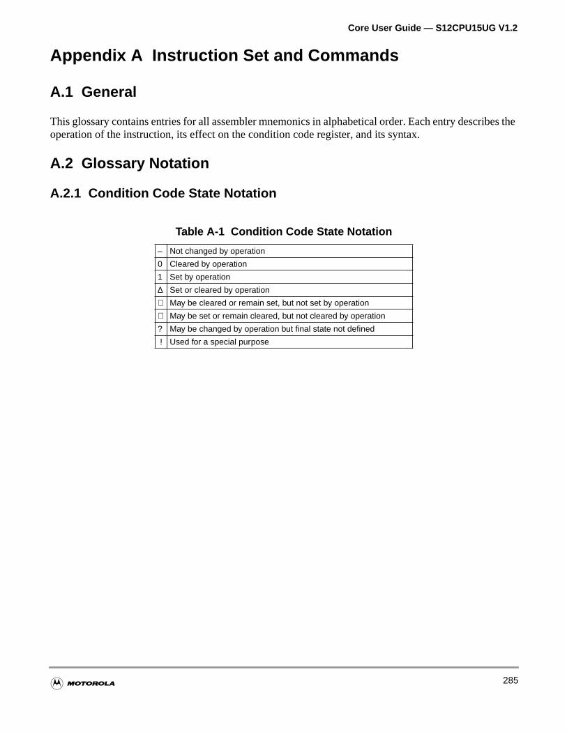
Core User Guide — S12CPU15UG V1.2
bes the
Appendix A Instruction Set and Commands
A.1 General
This glossary contains entries for all assembler mnemonics in alphabetical order. Each entry descrioperation of the instruction, its effect on the condition code register, and its syntax.
A.2 Glossary Notation
A.2.1 Condition Code State Notation
Table A-1 Condition Code State Notation
– Not changed by operation
0 Cleared by operation
1 Set by operation
∆ Set or cleared by operation
⇓ May be cleared or remain set, but not set by operation
⇑ May be set or remain cleared, but not cleared by operation
? May be changed by operation but final state not defined
! Used for a special purpose
285
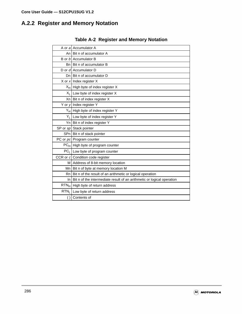
Core User Guide — S12CPU15UG V1.2
A.2.2 Register and Memory Notation
Table A-2 Register and Memory Notation
A or a Accumulator A
An Bit n of accumulator A
B or b Accumulator B
Bn Bit n of accumulator B
D or d Accumulator D
Dn Bit n of accumulator D
X or x Index register X
XH High byte of index register X
XL Low byte of index register X
Xn Bit n of index register X
Y or y Index register Y
YH High byte of index register Y
YL Low byte of index register Y
Yn Bit n of index register Y
SP or sp Stack pointer
SPn Bit n of stack pointer
PC or pc Program counter
PCH High byte of program counter
PCL Low byte of program counter
CCR or c Condition code register
M Address of 8-bit memory location
Mn Bit n of byte at memory location M
Rn Bit n of the result of an arithmetic or logical operation
In Bit n of the intermediate result of an arithmetic or logical operation
RTNH High byte of return address
RTNL Low byte of return address
( ) Contents of
286
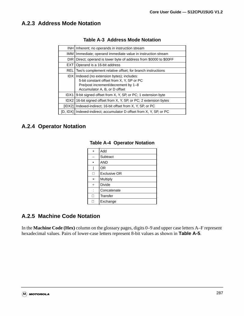
Core User Guide — S12CPU15UG V1.2
esent
A.2.3 Address Mode Notation
A.2.4 Operator Notation
A.2.5 Machine Code Notation
In theMachine Code (Hex)column on the glossary pages, digits 0–9 and upper case letters A–F reprhexadecimal values. Pairs of lower-case letters represent 8-bit values as shown inTable A-5 .
Table A-3 Address Mode Notation
INH Inherent; no operands in instruction stream
IMM Immediate; operand immediate value in instruction stream
DIR Direct; operand is lower byte of address from $0000 to $00FF
EXT Operand is a 16-bit address
REL Two’s complement relative offset; for branch instructions
IDX Indexed (no extension bytes); includes:5-bit constant offset from X, Y, SP or PCPre/post increment/decrement by 1–8Accumulator A, B, or D offset
IDX1 9-bit signed offset from X, Y, SP, or PC; 1 extension byte
IDX2 16-bit signed offset from X, Y, SP, or PC; 2 extension bytes
[IDX2] Indexed-indirect; 16-bit offset from X, Y, SP, or PC
[D, IDX] Indexed-indirect; accumulator D offset from X, Y, SP, or PC
Table A-4 Operator Notation
+ Add
– Subtract
• AND
| OR
⊕ Exclusive OR
× Multiply
÷ Divide
: Concatenate
⇒ Transfer
⇔ Exchange
287
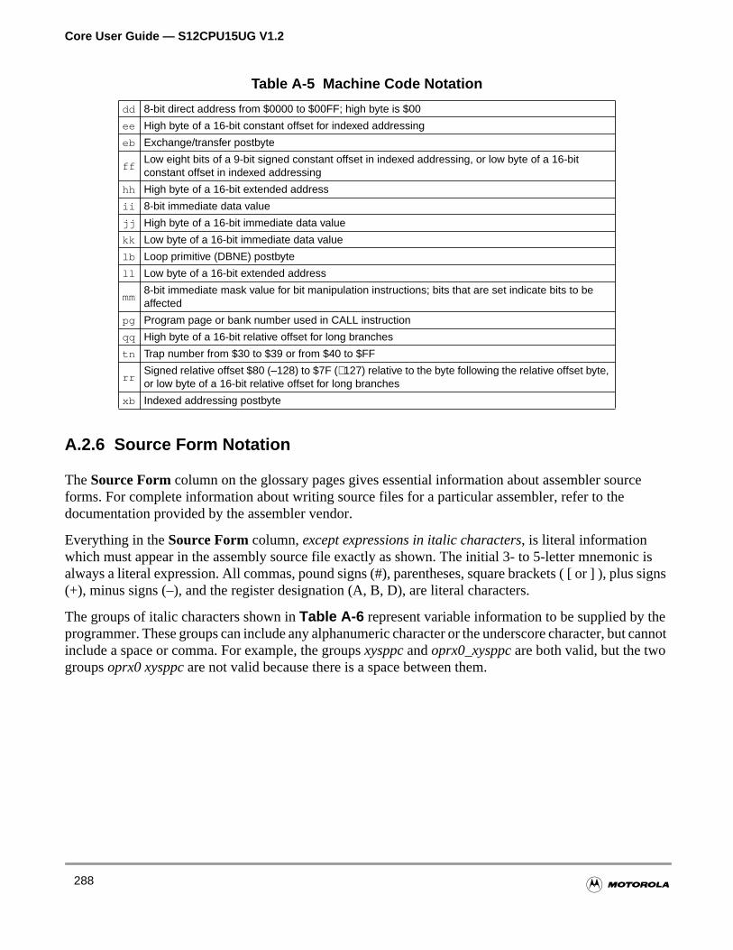
Core User Guide — S12CPU15UG V1.2
ce
ic is
et cannot
A.2.6 Source Form Notation
TheSource Form column on the glossary pages gives essential information about assembler sourforms. For complete information about writing source files for a particular assembler, refer to thedocumentation provided by the assembler vendor.
Everything in theSource Form column,except expressions in italic characters, is literal informationwhich must appear in the assembly source file exactly as shown. The initial 3- to 5-letter mnemonalways a literal expression. All commas, pound signs (#), parentheses, square brackets ( [ or ] ), plus signs(+), minus signs (–), and the register designation (A, B, D), are literal characters.
The groups of italic characters shown inTable A-6 represent variable information to be supplied by thprogrammer. These groups can include any alphanumeric character or the underscore character, buinclude a space or comma. For example, the groupsxysppcandoprx0_xysppcare both valid, but the twogroupsoprx0 xysppc are not valid because there is a space between them.
Table A-5 Machine Code Notation
dd 8-bit direct address from $0000 to $00FF; high byte is $00
ee High byte of a 16-bit constant offset for indexed addressing
eb Exchange/transfer postbyte
ffLow eight bits of a 9-bit signed constant offset in indexed addressing, or low byte of a 16-bitconstant offset in indexed addressing
hh High byte of a 16-bit extended address
ii 8-bit immediate data value
jj High byte of a 16-bit immediate data value
kk Low byte of a 16-bit immediate data value
lb Loop primitive (DBNE) postbyte
ll Low byte of a 16-bit extended address
mm8-bit immediate mask value for bit manipulation instructions; bits that are set indicate bits to beaffected
pg Program page or bank number used in CALL instruction
qq High byte of a 16-bit relative offset for long branches
tn Trap number from $30 to $39 or from $40 to $FF
rrSigned relative offset $80 (–128) to $7F (+127) relative to the byte following the relative offset byte,or low byte of a 16-bit relative offset for long branches
xb Indexed addressing postbyte
288
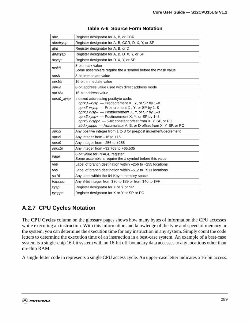
Core User Guide — S12CPU15UG V1.2
essesry incode
st-caseer than
access.
A.2.7 CPU Cycles Notation
TheCPU Cyclescolumn on the glossary pages shows how many bytes of information the CPU accwhile executing an instruction. With this information and knowledge of the type and speed of memothe system, you can determine the execution time for any instruction in any system. Simply count theletters to determine the execution time of an instruction in a best-case system. An example of a besystem is a single-chip 16-bit system with no 16-bit off-boundary data accesses to any locations othon-chip RAM.
A single-letter code in represents a single CPU access cycle. An upper-case letter indicates a 16-bit
Table A-6 Source Form Notation
abc Register designator for A, B, or CCR
abcdxysp Register designator for A, B, CCR, D, X, Y, or SP
abd Register designator for A, B, or D
abdxysp Register designator for A, B, D, X, Y, or SP
dxysp Register designator for D, X, Y, or SP
msk88-bit mask valueSome assemblers require the # symbol before the mask value.
opr8i 8-bit immediate value
opr16i 16-bit immediate value
opr8a 8-bit address value used with direct address mode
opr16a 16-bit address value
oprx0_xysp Indexed addressing postbyte code:oprx3,–xysp — Predecrement X , Y, or SP by 1–8oprx3,+xysp — Preincrement X , Y, or SP by 1–8oprx3,xysp– — Postdecrement X, Y, or SP by 1–8oprx3,xysp+ — Postincrement X, Y, or SP by 1–8oprx5,xysppc — 5-bit constant offset from X, Y, SP, or PCabd,xysppc — Accumulator A, B, or D offset from X, Y, SP, or PC
oprx3 Any positive integer from 1 to 8 for pre/post increment/decrement
oprx5 Any integer from –16 to +15
oprx9 Any integer from –256 to +255
oprx16 Any integer from –32,768 to +65,535
page8-bit value for PPAGE registerSome assemblers require the # symbol before this value.
rel8 Label of branch destination within –256 to +255 locations
rel9 Label of branch destination within –512 to +511 locations
rel16 Any label within the 64-Kbyte memory space
trapnum Any 8-bit integer from $30 to $39 or from $40 to $FF
xysp Register designator for X or Y or SP
xysppc Register designator for X or Y or SP or PC
289
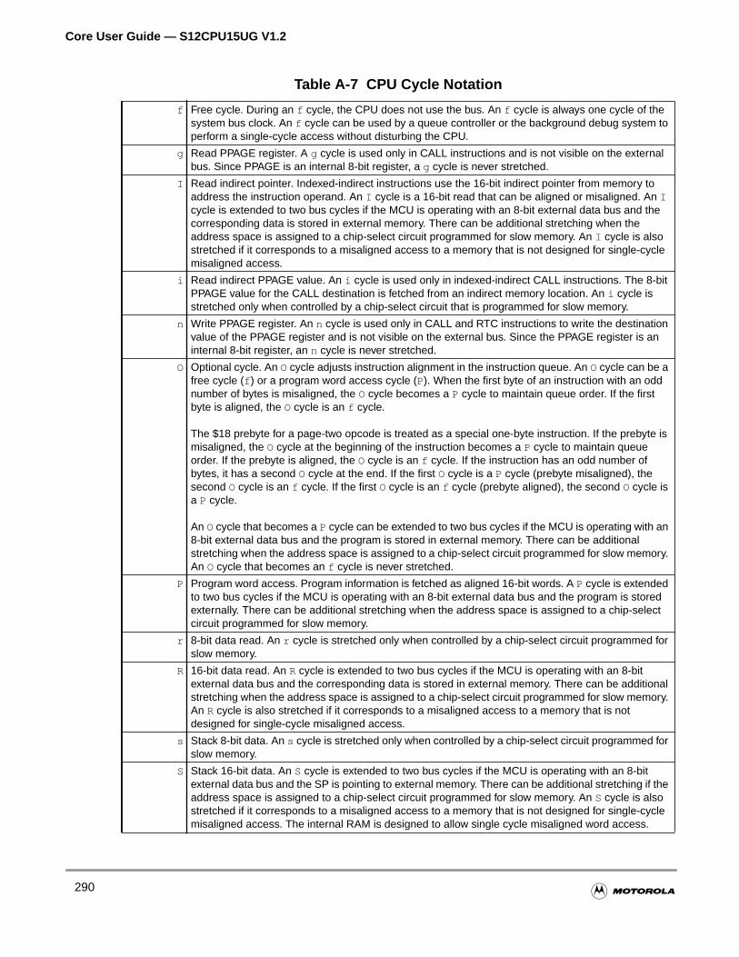
Core User Guide — S12CPU15UG V1.2
Table A-7 CPU Cycle Notation
f Free cycle. During an f cycle, the CPU does not use the bus. An f cycle is always one cycle of thesystem bus clock. An f cycle can be used by a queue controller or the background debug system toperform a single-cycle access without disturbing the CPU.
g Read PPAGE register. A g cycle is used only in CALL instructions and is not visible on the externalbus. Since PPAGE is an internal 8-bit register, a g cycle is never stretched.
I Read indirect pointer. Indexed-indirect instructions use the 16-bit indirect pointer from memory toaddress the instruction operand. An I cycle is a 16-bit read that can be aligned or misaligned. An Icycle is extended to two bus cycles if the MCU is operating with an 8-bit external data bus and thecorresponding data is stored in external memory. There can be additional stretching when theaddress space is assigned to a chip-select circuit programmed for slow memory. An I cycle is alsostretched if it corresponds to a misaligned access to a memory that is not designed for single-cyclemisaligned access.
i Read indirect PPAGE value. An i cycle is used only in indexed-indirect CALL instructions. The 8-bitPPAGE value for the CALL destination is fetched from an indirect memory location. An i cycle isstretched only when controlled by a chip-select circuit that is programmed for slow memory.
n Write PPAGE register. An n cycle is used only in CALL and RTC instructions to write the destinationvalue of the PPAGE register and is not visible on the external bus. Since the PPAGE register is aninternal 8-bit register, an n cycle is never stretched.
O Optional cycle. An Ocycle adjusts instruction alignment in the instruction queue. An Ocycle can be afree cycle (f ) or a program word access cycle (P). When the first byte of an instruction with an oddnumber of bytes is misaligned, the O cycle becomes a P cycle to maintain queue order. If the firstbyte is aligned, the O cycle is an f cycle.
The $18 prebyte for a page-two opcode is treated as a special one-byte instruction. If the prebyte ismisaligned, the O cycle at the beginning of the instruction becomes a P cycle to maintain queueorder. If the prebyte is aligned, the O cycle is an f cycle. If the instruction has an odd number ofbytes, it has a second O cycle at the end. If the first O cycle is a P cycle (prebyte misaligned), thesecond Ocycle is an f cycle. If the first Ocycle is an f cycle (prebyte aligned), the second Ocycle isa P cycle.
An Ocycle that becomes a P cycle can be extended to two bus cycles if the MCU is operating with an8-bit external data bus and the program is stored in external memory. There can be additionalstretching when the address space is assigned to a chip-select circuit programmed for slow memory.An O cycle that becomes an f cycle is never stretched.
P Program word access. Program information is fetched as aligned 16-bit words. A P cycle is extendedto two bus cycles if the MCU is operating with an 8-bit external data bus and the program is storedexternally. There can be additional stretching when the address space is assigned to a chip-selectcircuit programmed for slow memory.
r 8-bit data read. An r cycle is stretched only when controlled by a chip-select circuit programmed forslow memory.
R 16-bit data read. An R cycle is extended to two bus cycles if the MCU is operating with an 8-bitexternal data bus and the corresponding data is stored in external memory. There can be additionalstretching when the address space is assigned to a chip-select circuit programmed for slow memory.An R cycle is also stretched if it corresponds to a misaligned access to a memory that is notdesigned for single-cycle misaligned access.
s Stack 8-bit data. An s cycle is stretched only when controlled by a chip-select circuit programmed forslow memory.
S Stack 16-bit data. An S cycle is extended to two bus cycles if the MCU is operating with an 8-bitexternal data bus and the SP is pointing to external memory. There can be additional stretching if theaddress space is assigned to a chip-select circuit programmed for slow memory. An S cycle is alsostretched if it corresponds to a misaligned access to a memory that is not designed for single-cyclemisaligned access. The internal RAM is designed to allow single cycle misaligned word access.
290
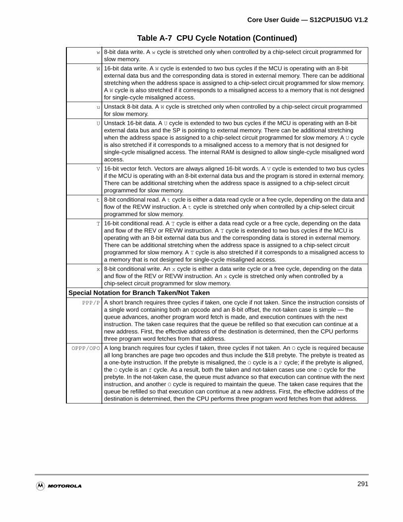
Core User Guide — S12CPU15UG V1.2
w 8-bit data write. A w cycle is stretched only when controlled by a chip-select circuit programmed forslow memory.
W 16-bit data write. A W cycle is extended to two bus cycles if the MCU is operating with an 8-bitexternal data bus and the corresponding data is stored in external memory. There can be additionalstretching when the address space is assigned to a chip-select circuit programmed for slow memory.A Wcycle is also stretched if it corresponds to a misaligned access to a memory that is not designedfor single-cycle misaligned access.
u Unstack 8-bit data. A W cycle is stretched only when controlled by a chip-select circuit programmedfor slow memory.
U Unstack 16-bit data. A U cycle is extended to two bus cycles if the MCU is operating with an 8-bitexternal data bus and the SP is pointing to external memory. There can be additional stretchingwhen the address space is assigned to a chip-select circuit programmed for slow memory. A U cycleis also stretched if it corresponds to a misaligned access to a memory that is not designed forsingle-cycle misaligned access. The internal RAM is designed to allow single-cycle misaligned wordaccess.
V 16-bit vector fetch. Vectors are always aligned 16-bit words. A V cycle is extended to two bus cyclesif the MCU is operating with an 8-bit external data bus and the program is stored in external memory.There can be additional stretching when the address space is assigned to a chip-select circuitprogrammed for slow memory.
t 8-bit conditional read. A t cycle is either a data read cycle or a free cycle, depending on the data andflow of the REVW instruction. A t cycle is stretched only when controlled by a chip-select circuitprogrammed for slow memory.
T 16-bit conditional read. A T cycle is either a data read cycle or a free cycle, depending on the dataand flow of the REV or REVW instruction. A T cycle is extended to two bus cycles if the MCU isoperating with an 8-bit external data bus and the corresponding data is stored in external memory.There can be additional stretching when the address space is assigned to a chip-select circuitprogrammed for slow memory. A T cycle is also stretched if it corresponds to a misaligned access toa memory that is not designed for single-cycle misaligned access.
x 8-bit conditional write. An x cycle is either a data write cycle or a free cycle, depending on the dataand flow of the REV or REVW instruction. An x cycle is stretched only when controlled by achip-select circuit programmed for slow memory.
Special Notation for Branch Taken/Not TakenPPP/P A short branch requires three cycles if taken, one cycle if not taken. Since the instruction consists of
a single word containing both an opcode and an 8-bit offset, the not-taken case is simple — thequeue advances, another program word fetch is made, and execution continues with the nextinstruction. The taken case requires that the queue be refilled so that execution can continue at anew address. First, the effective address of the destination is determined, then the CPU performsthree program word fetches from that address.
OPPP/OPO A long branch requires four cycles if taken, three cycles if not taken. An O cycle is required becauseall long branches are page two opcodes and thus include the $18 prebyte. The prebyte is treated asa one-byte instruction. If the prebyte is misaligned, the O cycle is a P cycle; if the prebyte is aligned,the O cycle is an f cycle. As a result, both the taken and not-taken cases use one O cycle for theprebyte. In the not-taken case, the queue must advance so that execution can continue with the nextinstruction, and another O cycle is required to maintain the queue. The taken case requires that thequeue be refilled so that execution can continue at a new address. First, the effective address of thedestination is determined, then the CPU performs three program word fetches from that address.
Table A-7 CPU Cycle Notation (Continued)
291
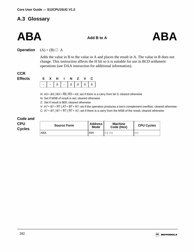
Core User Guide — S12CPU15UG V1.2
not
A.3 Glossary
Operation (A) + (B) ⇒ A
Adds the value in B to the value in A and places the result in A. The value in B doeschange. This instruction affects the H bit so it is suitable for use in BCD arithmeticoperations (see DAA instruction for additional information).
CCREffects
Code andCPUCycles
ABA Add B to A ABA
S X H I N Z V C
– – ∆ – ∆ ∆ ∆ ∆
H: A3 • B3 | B3 • R3 | R3 • A3; set if there is a carry from bit 3; cleared otherwiseN: Set if MSB of result is set; cleared otherwiseZ: Set if result is $00; cleared otherwiseV: A7 • B7 • R7 | A7 • B7 • R7; set if the operation produces a two’s complement overflow; cleared otherwiseC: A7 • B7 | B7 • R7 | R7 • A7; set if there is a carry from the MSB of the result; cleared otherwise
Source Form AddressMode
MachineCode (Hex) CPU Cycles
ABA INH 18 06 OO
292
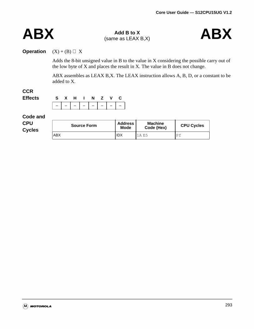
Core User Guide — S12CPU15UG V1.2
ut of
e
Operation (X) + (B) ⇒ X
Adds the 8-bit unsigned value in B to the value in X considering the possible carry othe low byte of X and places the result in X. The value in B does not change.
ABX assembles as LEAX B,X. The LEAX instruction allows A, B, D, or a constant to badded to X.
CCREffects
Code andCPUCycles
ABX Add B to X(same as LEAX B,X) ABX
S X H I N Z V C
– – – – – – – –
Source Form AddressMode
MachineCode (Hex) CPU Cycles
ABX IDX 1A E5 Pf
293
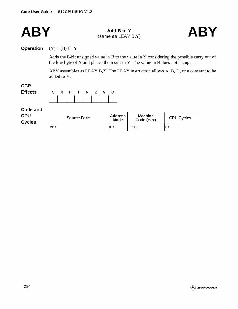
Core User Guide — S12CPU15UG V1.2
ut of
e
Operation (Y) + (B) ⇒ Y
Adds the 8-bit unsigned value in B to the value in Y considering the possible carry othe low byte of Y and places the result in Y. The value in B does not change.
ABY assembles as LEAY B,Y. The LEAY instruction allows A, B, D, or a constant to badded to Y.
CCREffects
Code andCPUCycles
ABY Add B to Y(same as LEAY B,Y) ABY
S X H I N Z V C
– – – – – – – –
Source Form AddressMode
MachineCode (Hex) CPU Cycles
ABY IDX 19 ED Pf
294
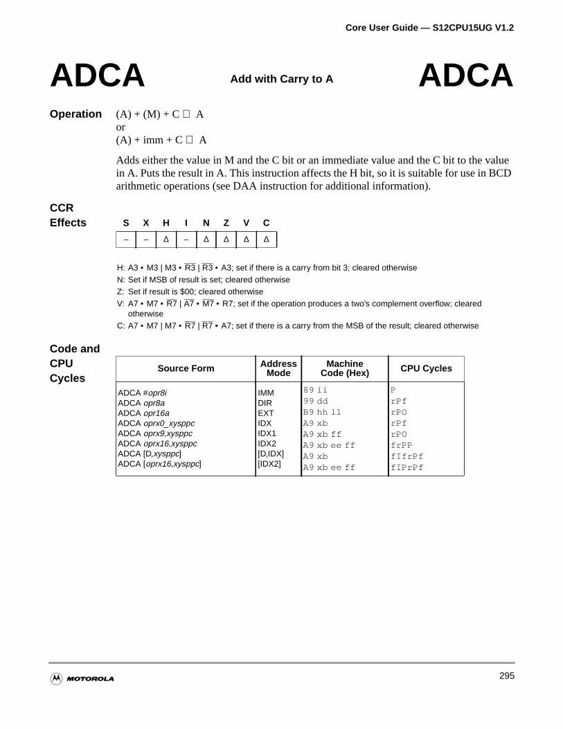
Core User Guide — S12CPU15UG V1.2
alueD
Operation (A) + (M) + C ⇒ Aor(A) + imm + C⇒ A
Adds either the value in M and the C bit or an immediate value and the C bit to the vin A. Puts the result in A. This instruction affects the H bit, so it is suitable for use in BCarithmetic operations (see DAA instruction for additional information).
CCREffects
Code andCPUCycles
ADCA Add with Carry to A ADCA
S X H I N Z V C
– – ∆ – ∆ ∆ ∆ ∆
H: A3 • M3 | M3 • R3 | R3 • A3; set if there is a carry from bit 3; cleared otherwiseN: Set if MSB of result is set; cleared otherwiseZ: Set if result is $00; cleared otherwiseV: A7 • M7 • R7 | A7 • M7 • R7; set if the operation produces a two’s complement overflow; cleared
otherwiseC: A7 • M7 | M7 • R7 | R7 • A7; set if there is a carry from the MSB of the result; cleared otherwise
Source Form AddressMode
MachineCode (Hex) CPU Cycles
ADCA #opr8iADCA opr8aADCA opr16aADCA oprx0_xysppcADCA oprx9,xysppcADCA oprx16,xysppcADCA [D,xysppc]ADCA [oprx16,xysppc]
IMMDIREXTIDXIDX1IDX2[D,IDX][IDX2]
89 ii99 ddB9 hh llA9 xbA9 xb ffA9 xb ee ffA9 xbA9 xb ee ff
PrPfrPOrPfrPOfrPPfIfrPffIPrPf
295
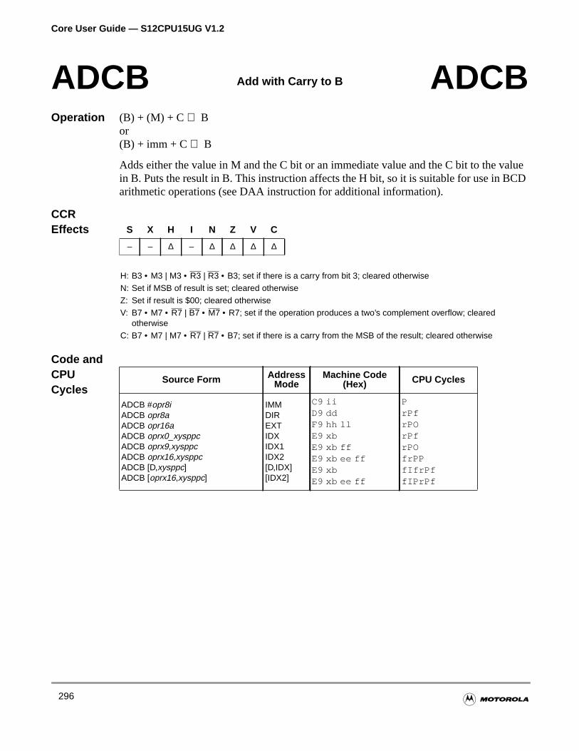
Core User Guide — S12CPU15UG V1.2
alueCD
Operation (B) + (M) + C⇒ Bor(B) + imm + C⇒ B
Adds either the value in M and the C bit or an immediate value and the C bit to the vin B. Puts the result in B. This instruction affects the H bit, so it is suitable for use in Barithmetic operations (see DAA instruction for additional information).
CCREffects
Code andCPUCycles
ADCB Add with Carry to B ADCB
S X H I N Z V C
– – ∆ – ∆ ∆ ∆ ∆
H: B3 • M3 | M3 • R3 | R3 • B3; set if there is a carry from bit 3; cleared otherwiseN: Set if MSB of result is set; cleared otherwiseZ: Set if result is $00; cleared otherwiseV: B7 • M7 • R7 | B7 • M7 • R7; set if the operation produces a two’s complement overflow; cleared
otherwiseC: B7 • M7 | M7 • R7 | R7 • B7; set if there is a carry from the MSB of the result; cleared otherwise
Source Form AddressMode
Machine Code(Hex) CPU Cycles
ADCB #opr8iADCB opr8aADCB opr16aADCB oprx0_xysppcADCB oprx9,xysppcADCB oprx16,xysppcADCB [D,xysppc]ADCB [oprx16,xysppc]
IMMDIREXTIDXIDX1IDX2[D,IDX][IDX2]
C9 iiD9 ddF9 hh llE9 xbE9 xb ffE9 xb ee ffE9 xbE9 xb ee ff
PrPfrPOrPfrPOfrPPfIfrPffIPrPf
296
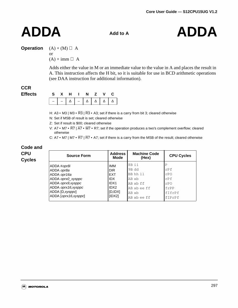
Core User Guide — S12CPU15UG V1.2
lt inions
Operation (A) + (M) ⇒ Aor(A) + imm ⇒ A
Adds either the value in M or an immediate value to the value in A and places the resuA. This instruction affects the H bit, so it is suitable for use in BCD arithmetic operat(see DAA instruction for additional information).
CCREffects
Code andCPUCycles
ADDA Add to A ADDA
S X H I N Z V C
– – ∆ – ∆ ∆ ∆ ∆
H: A3 • M3 | M3 • R3 | R3 • A3; set if there is a carry from bit 3; cleared otherwiseN: Set if MSB of result is set; cleared otherwiseZ: Set if result is $00; cleared otherwiseV: A7 • M7 • R7 | A7 • M7 • R7; set if the operation produces a two’s complement overflow; cleared
otherwiseC: A7 • M7 | M7 • R7 | R7 • A7; set if there is a carry from the MSB of the result; cleared otherwise
Source Form AddressMode
Machine Code(Hex) CPU Cycles
ADDA #opr8iADDA opr8aADDA opr16aADDA oprx0_xysppcADDA oprx9,xysppcADDA oprx16,xysppcADDA [D,xysppc]ADDA [oprx16,xysppc]
IMMDIREXTIDXIDX1IDX2[D,IDX][IDX2]
8B ii9B ddBB hh llAB xbAB xb ffAB xb ee ffAB xbAB xb ee ff
PrPfrPOrPfrPOfrPPfIfrPffIPrPf
297
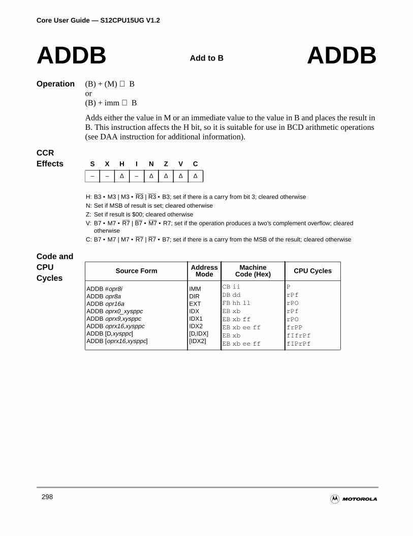
Core User Guide — S12CPU15UG V1.2
lt inions
Operation (B) + (M) ⇒ Bor(B) + imm⇒ B
Adds either the value in M or an immediate value to the value in B and places the resuB. This instruction affects the H bit, so it is suitable for use in BCD arithmetic operat(see DAA instruction for additional information).
CCREffects
Code andCPUCycles
ADDB Add to B ADDB
S X H I N Z V C
– – ∆ – ∆ ∆ ∆ ∆
H: B3 • M3 | M3 • R3 | R3 • B3; set if there is a carry from bit 3; cleared otherwiseN: Set if MSB of result is set; cleared otherwiseZ: Set if result is $00; cleared otherwiseV: B7 • M7 • R7 | B7 • M7 • R7; set if the operation produces a two’s complement overflow; cleared
otherwiseC: B7 • M7 | M7 • R7 | R7 • B7; set if there is a carry from the MSB of the result; cleared otherwise
Source Form AddressMode
MachineCode (Hex) CPU Cycles
ADDB #opr8iADDB opr8aADDB opr16aADDB oprx0_xysppcADDB oprx9,xysppcADDB oprx16,xysppcADDB [D,xysppc]ADDB [oprx16,xysppc]
IMMDIREXTIDXIDX1IDX2[D,IDX][IDX2]
CB iiDB ddFB hh llEB xbEB xb ffEB xb ee ffEB xbEB xb ee ff
PrPfrPOrPfrPOfrPPfIfrPffIPrPf
298
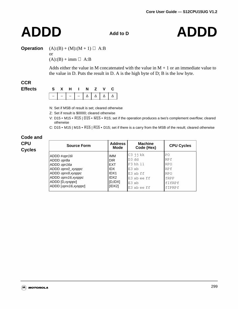
Core User Guide — S12CPU15UG V1.2
e to
Operation (A):(B) + (M):(M + 1) ⇒ A:Bor(A):(B) + imm ⇒ A:B
Adds either the value in M concatenated with the value in M + 1 or an immediate valuthe value in D. Puts the result in D. A is the high byte of D; B is the low byte.
CCREffects
Code andCPUCycles
ADDD Add to D ADDD
S X H I N Z V C
– – – – ∆ ∆ ∆ ∆
N: Set if MSB of result is set; cleared otherwiseZ: Set if result is $0000; cleared otherwiseV: D15 • M15 • R15 | D15 • M15 • R15; set if the operation produces a two’s complement overflow; cleared
otherwiseC: D15 • M15 | M15 • R15 | R15 • D15; set if there is a carry from the MSB of the result; cleared otherwise
Source Form AddressMode
MachineCode (Hex) CPU Cycles
ADDD #opr16iADDD opr8aADDD opr16aADDD oprx0_xysppcADDD oprx9,xysppcADDD oprx16,xysppcADDD [D,xysppc]ADDD [oprx16,xysppc]
IMMDIREXTIDXIDX1IDX2[D,IDX][IDX2]
C3 jj kkD3 ddF3 hh llE3 xbE3 xb ffE3 xb ee ffE3 xbE3 xb ee ff
PORPfRPORPfRPOfRPPfIfRPffIPRPf
299

Core User Guide — S12CPU15UG V1.2
in
Operation (A) • (M) ⇒ Aor(A) • imm ⇒ A
Performs a logical AND of either the value in M or an immediate value with the valueA. Puts the result in A.
CCREffects
Code andCPUCycles
ANDA AND with A ANDA
S X H I N Z V C
– – – – ∆ ∆ 0 –
N: Set if MSB of result is set; cleared otherwiseZ: Set if result is $00; cleared otherwiseV: Cleared
Source Form AddressMode
MachineCode (Hex) CPU Cycles
ANDA #opr8iANDA opr8aANDA opr16aANDA oprx0_xysppcANDA oprx9,xysppcANDA oprx16,xysppcANDA [D,xysppc]ANDA [oprx16,xysppc]
IMMDIREXTIDXIDX1IDX2[D,IDX][IDX2]
84 ii94 ddB4 hh llA4 xbA4 xb ffA4 xb ee ffA4 xbA4 xb ee ff
PrPfrPOrPfrPOfrPPfIfrPffIPrPf
300

Core User Guide — S12CPU15UG V1.2
in
Operation (B) • (M) ⇒ Bor(B) • imm ⇒ B
Performs a logical AND of either the value in M or an immediate value with the valueB. Puts the result in B.
CCREffects
Code andCPUCycles
ANDB AND with B ANDB
S X H I N Z V C
– – – – ∆ ∆ 0 –
N: Set if MSB of result is set; cleared otherwiseZ: Set if result is $00; cleared otherwiseV: Cleared
Source Form AddressMode
MachineCode (Hex) CPU Cycles
ANDB #opr8iANDB opr8aANDB opr16aANDB oprx0_xysppcANDB oprx9,xysppcANDB oprx16,xysppcANDB [D,xysppc]ANDB [oprx16,xysppc]
IMMDIREXTIDXIDX1IDX2[D,IDX][IDX2]
C4 iiD4 ddF4 hh llE4 xbE4 xb ffE4 xb ee ffE4 xbE4 xb ee ff
PrPfrPOrPfrPOfrPPfIfrPffIPrPf
301
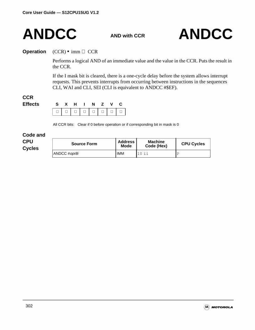
Core User Guide — S12CPU15UG V1.2
lt in
uptces
Operation (CCR)• imm ⇒ CCR
Performs a logical AND of an immediate value and the value in the CCR. Puts the resuthe CCR.
If the I mask bit is cleared, there is a one-cycle delay before the system allows interrrequests. This prevents interrupts from occurring between instructions in the sequenCLI, WAI and CLI, SEI (CLI is equivalent to ANDCC #$EF).
CCREffects
Code andCPUCycles
ANDCC AND with CCR ANDCC
S X H I N Z V C
⇓ ⇓ ⇓ ⇓ ⇓ ⇓ ⇓ ⇓
All CCR bits: Clear if 0 before operation or if corresponding bit in mask is 0
Source Form AddressMode
MachineCode (Hex) CPU Cycles
ANDCC #opr8i IMM 10 ii P
302

Core User Guide — S12CPU15UG V1.2
ed
Operation
Shifts all bits of M one bit position to the left. Bit 0 is loaded with a 0. The C bit is loadfrom the most significant bit of M.
CCREffects
Code andCPUCycles
ASL Arithmetic Shift Left M(same as LSL) ASL
b7 b6 b5 b4 b3 b2 b1 b0C 0
M
S X H I N Z V C
– – – – ∆ ∆ ∆ ∆
N: Set if MSB of result is set; cleared otherwiseZ: Set if result is $00; cleared otherwiseV: N ⊕ C; set if:
N is set and C is cleared after the shift, orN is cleared and C is set after the shift; cleared otherwise
C: M7; set if the MSB of M was set before the shift; cleared otherwise
Source Form AddressMode
MachineCode (Hex) CPU Cycles
ASL opr16aASL oprx0_xysppcASL oprx9,xysppcASL oprx16,xysppcASL [D,xysppc]ASL [oprx16,xysppc]
EXTIDXIDX1IDX2[D,IDX][IDX2]
78 hh ll68 xb68 xb ff68 xb ee ff68 xb68 xb ee ff
rPwOrPwrPwOfrPwPfIfrPwfIPrPw
303
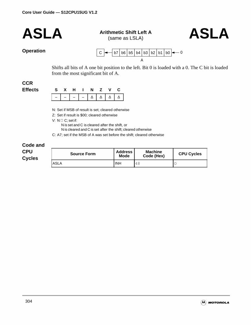
Core User Guide — S12CPU15UG V1.2
ed
Operation
Shifts all bits of A one bit position to the left. Bit 0 is loaded with a 0. The C bit is loadfrom the most significant bit of A.
CCREffects
Code andCPUCycles
ASLA Arithmetic Shift Left A(same as LSLA) ASLA
b7 b6 b5 b4 b3 b2 b1 b0C 0
A
S X H I N Z V C
– – – – ∆ ∆ ∆ ∆
N: Set if MSB of result is set; cleared otherwiseZ: Set if result is $00; cleared otherwiseV: N ⊕ C; set if:
N is set and C is cleared after the shift, orN is cleared and C is set after the shift; cleared otherwise
C: A7; set if the MSB of A was set before the shift; cleared otherwise
Source Form AddressMode
MachineCode (Hex) CPU Cycles
ASLA INH 48 O
304
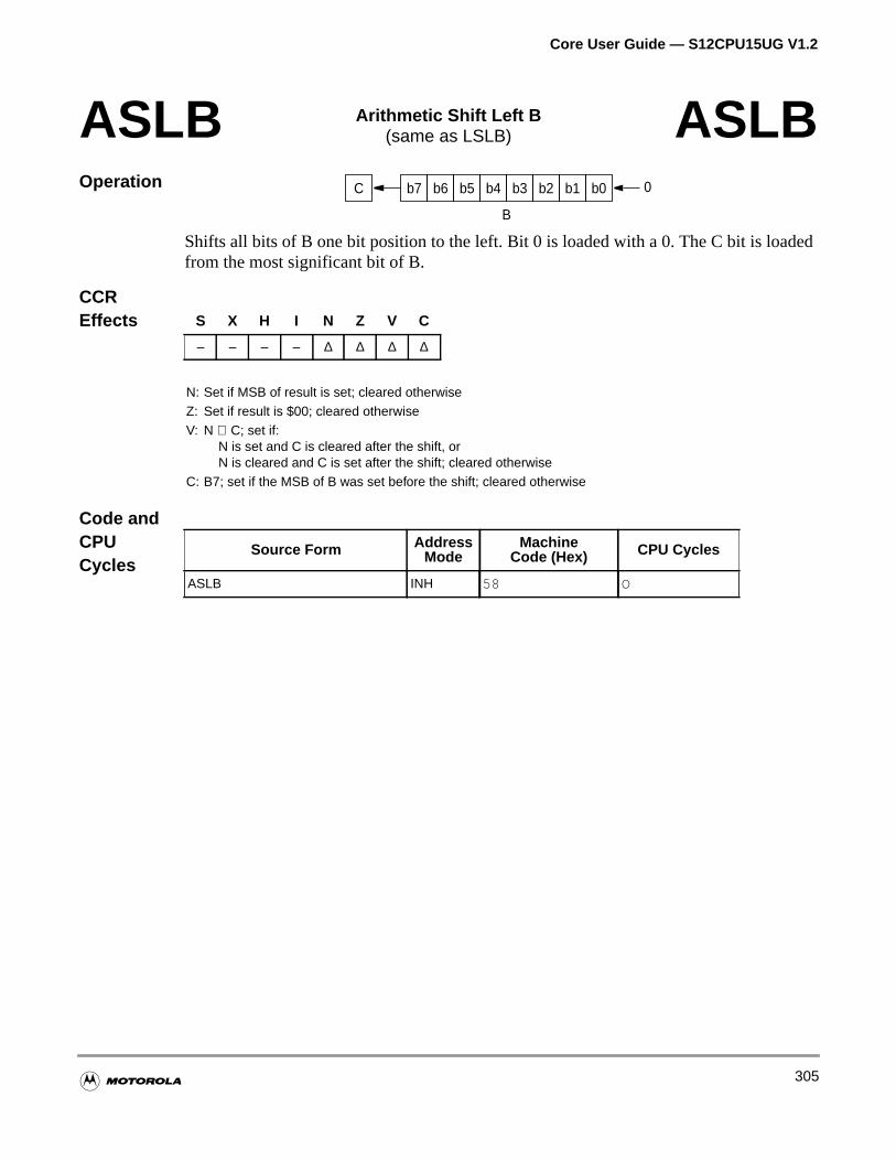
Core User Guide — S12CPU15UG V1.2
ded
Operation
Shifts all bits of B one bit position to the left. Bit 0 is loaded with a 0. The C bit is loafrom the most significant bit of B.
CCREffects
Code andCPUCycles
ASLB Arithmetic Shift Left B(same as LSLB) ASLB
b7 b6 b5 b4 b3 b2 b1 b0C 0
B
S X H I N Z V C
– – – – ∆ ∆ ∆ ∆
N: Set if MSB of result is set; cleared otherwiseZ: Set if result is $00; cleared otherwiseV: N ⊕ C; set if:
N is set and C is cleared after the shift, orN is cleared and C is set after the shift; cleared otherwise
C: B7; set if the MSB of B was set before the shift; cleared otherwise
Source Form AddressMode
MachineCode (Hex) CPU Cycles
ASLB INH 58 O
305
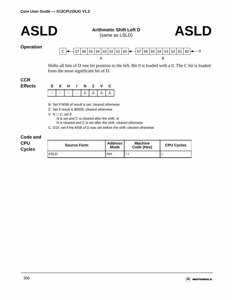
Core User Guide — S12CPU15UG V1.2
ed
Operation
Shifts all bits of D one bit position to the left. Bit 0 is loaded with a 0. The C bit is loadfrom the most significant bit of D.
CCREffects
Code andCPUCycles
ASLD Arithmetic Shift Left D(same as LSLD) ASLD
0b7 b6 b5 b4 b3 b2 b1 b0 b7 b6 b5 b4 b3 b2 b1 b0C
BA
S X H I N Z V C
– – – – ∆ ∆ ∆ ∆
N: Set if MSB of result is set; cleared otherwiseZ: Set if result is $0000; cleared otherwiseV: N ⊕ C; set if:
N is set and C is cleared after the shift, orN is cleared and C is set after the shift; cleared otherwise
C: D15; set if the MSB of D was set before the shift; cleared otherwise
Source Form AddressMode
MachineCode (Hex) CPU Cycles
ASLD INH 59 O
306
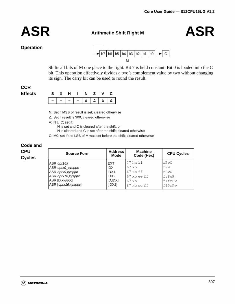
Core User Guide — S12CPU15UG V1.2
e Cing
Operation
Shifts all bits of M one place to the right. Bit 7 is held constant. Bit 0 is loaded into thbit. This operation effectively divides a two’s complement value by two without changits sign. The carry bit can be used to round the result.
CCREffects
Code andCPUCycles
ASR Arithmetic Shift Right M ASRb7 b6 b5 b4 b3 b2 b1 b0 C
M
S X H I N Z V C
– – – – ∆ ∆ ∆ ∆
N: Set if MSB of result is set; cleared otherwiseZ: Set if result is $00; cleared otherwiseV: N ⊕ C; set if:
N is set and C is cleared after the shift, orN is cleared and C is set after the shift; cleared otherwise
C: M0; set if the LSB of M was set before the shift; cleared otherwise
Source Form AddressMode
MachineCode (Hex) CPU Cycles
ASR opr16aASR oprx0_xysppcASR oprx9,xysppcASR oprx16,xysppcASR [D,xysppc]ASR [oprx16,xysppc]
EXTIDXIDX1IDX2[D,IDX][IDX2]
77 hh ll67 xb67 xb ff67 xb ee ff67 xb67 xb ee ff
rPwOrPwrPwOfrPwPfIfrPwfIPrPw
307
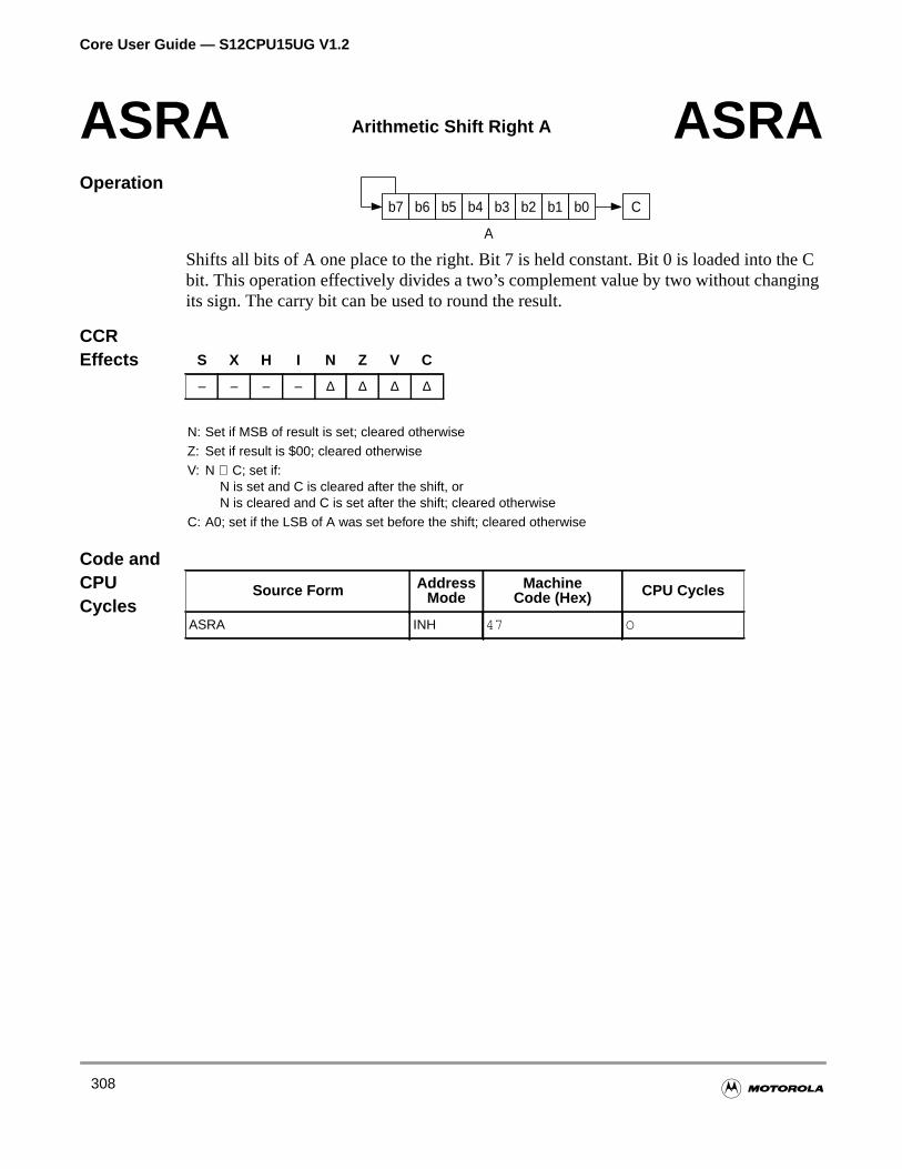
Core User Guide — S12CPU15UG V1.2
e Cing
Operation
Shifts all bits of A one place to the right. Bit 7 is held constant. Bit 0 is loaded into thbit. This operation effectively divides a two’s complement value by two without changits sign. The carry bit can be used to round the result.
CCREffects
Code andCPUCycles
ASRA Arithmetic Shift Right A ASRAb7 b6 b5 b4 b3 b2 b1 b0 C
A
S X H I N Z V C
– – – – ∆ ∆ ∆ ∆
N: Set if MSB of result is set; cleared otherwiseZ: Set if result is $00; cleared otherwiseV: N ⊕ C; set if:
N is set and C is cleared after the shift, orN is cleared and C is set after the shift; cleared otherwise
C: A0; set if the LSB of A was set before the shift; cleared otherwise
Source Form AddressMode
MachineCode (Hex) CPU Cycles
ASRA INH 47 O
308
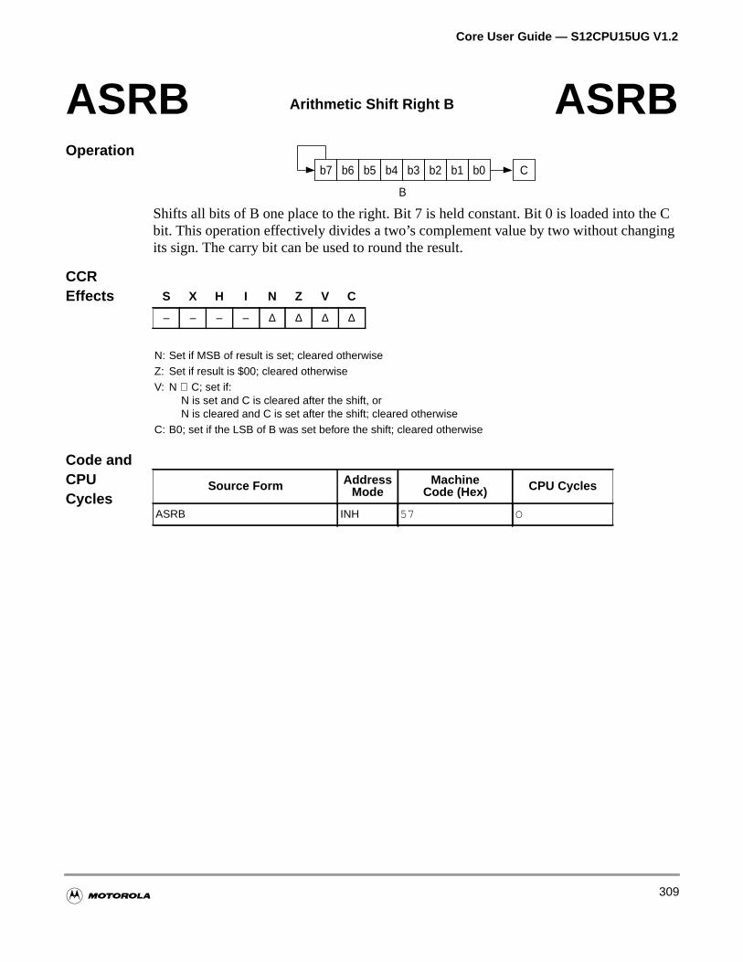
Core User Guide — S12CPU15UG V1.2
e Cing
Operation
Shifts all bits of B one place to the right. Bit 7 is held constant. Bit 0 is loaded into thbit. This operation effectively divides a two’s complement value by two without changits sign. The carry bit can be used to round the result.
CCREffects
Code andCPUCycles
ASRB Arithmetic Shift Right B ASRBb7 b6 b5 b4 b3 b2 b1 b0 C
B
S X H I N Z V C
– – – – ∆ ∆ ∆ ∆
N: Set if MSB of result is set; cleared otherwiseZ: Set if result is $00; cleared otherwiseV: N ⊕ C; set if:
N is set and C is cleared after the shift, orN is cleared and C is set after the shift; cleared otherwise
C: B0; set if the LSB of B was set before the shift; cleared otherwise
Source Form AddressMode
MachineCode (Hex) CPU Cycles
ASRB INH 57 O
309

Core User Guide — S12CPU15UG V1.2
y. of
Operation If C = 0, then (PC) + $0002 + rel⇒ PC
Tests the C bit and branches if C = 0.
Rel is an 8-bit two’s complement offset for branching forward or backward in memorBranching range is $80 to $7F (–128 to 127) from the address following the last byteobject code in the instruction.
CCREffects
Code andCPUCycles
BCC Branch if C Clear(same as BHS) BCC
S X H I N Z V C
– – – – – – – –
Source Form AddressMode
MachineCode (Hex) CPU Cycles
BCC rel8 REL24 rr PPP (branch)
P (no branch)
Branch Complementary BranchComment
Mnemonic Opcode Test Mnemonic Opcode Test
BCC/BHS 24
(R) ≥ (M)or(B) ≥ (A) BCS/BLO 25
(R) < (M)or(B) < (A) Unsigned
C = 0 C = 1
BGE 2C
(R) ≥ (M)or(B) ≥ (A) BLT 2D
(R) < (M)or(B) < (A) Signed
N ⊕ V = 0 N ⊕ V = 1
310
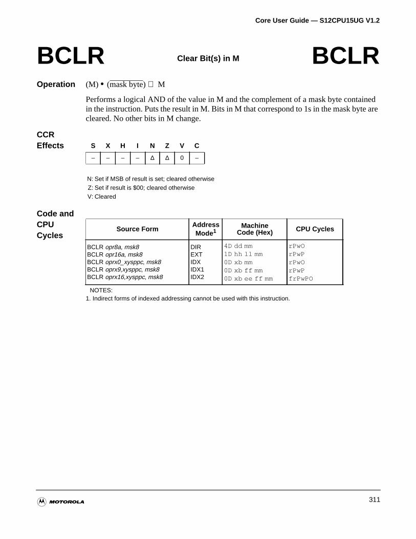
Core User Guide — S12CPU15UG V1.2
inedare
Operation (M) • (mask byte)⇒ M
Performs a logical AND of the value in M and the complement of a mask byte contain the instruction. Puts the result in M. Bits in M that correspond to 1s in the mask bytecleared. No other bits in M change.
CCREffects
Code andCPUCycles
BCLR Clear Bit(s) in M BCLR
S X H I N Z V C
– – – – ∆ ∆ 0 –
N: Set if MSB of result is set; cleared otherwiseZ: Set if result is $00; cleared otherwiseV: Cleared
Source FormAddressMode1
NOTES:1. Indirect forms of indexed addressing cannot be used with this instruction.
MachineCode (Hex) CPU Cycles
BCLR opr8a, msk8BCLR opr16a, msk8BCLR oprx0_xysppc, msk8BCLR oprx9,xysppc, msk8BCLR oprx16,xysppc, msk8
DIREXTIDXIDX1IDX2
4D dd mm1D hh ll mm0D xb mm0D xb ff mm0D xb ee ff mm
rPwOrPwPrPwOrPwPfrPwPO
311
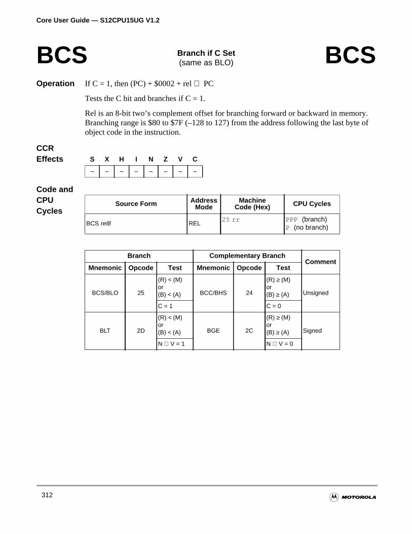
Core User Guide — S12CPU15UG V1.2
y. of
Operation If C = 1, then (PC) + $0002 + rel⇒ PC
Tests the C bit and branches if C = 1.
Rel is an 8-bit two’s complement offset for branching forward or backward in memorBranching range is $80 to $7F (–128 to 127) from the address following the last byteobject code in the instruction.
CCREffects
Code andCPUCycles
BCS Branch if C Set(same as BLO) BCS
S X H I N Z V C
– – – – – – – –
Source Form AddressMode
MachineCode (Hex) CPU Cycles
BCS rel8 REL25 rr PPP (branch)
P (no branch)
Branch Complementary BranchComment
Mnemonic Opcode Test Mnemonic Opcode Test
BCS/BLO 25
(R) < (M)or(B) < (A) BCC/BHS 24
(R) ≥ (M)or(B) ≥ (A) Unsigned
C = 1 C = 0
BLT 2D
(R) < (M)or(B) < (A) BGE 2C
(R) ≥ (M)or(B) ≥ (A) Signed
N ⊕ V = 1 N ⊕ V = 0
312
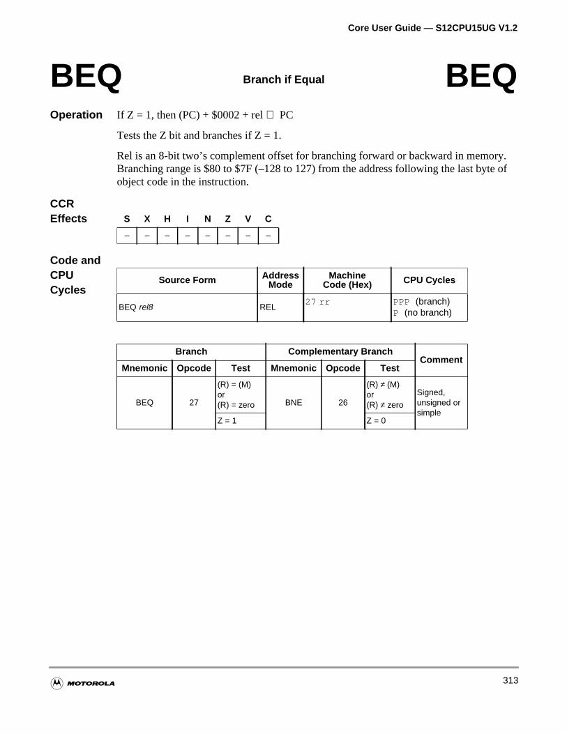
Core User Guide — S12CPU15UG V1.2
y. of
Operation If Z = 1, then (PC) + $0002 + rel⇒ PC
Tests the Z bit and branches if Z = 1.
Rel is an 8-bit two’s complement offset for branching forward or backward in memorBranching range is $80 to $7F (–128 to 127) from the address following the last byteobject code in the instruction.
CCREffects
Code andCPUCycles
BEQ Branch if Equal BEQ
S X H I N Z V C
– – – – – – – –
Source Form AddressMode
MachineCode (Hex) CPU Cycles
BEQ rel8 REL27 rr PPP (branch)
P (no branch)
Branch Complementary BranchComment
Mnemonic Opcode Test Mnemonic Opcode Test
BEQ 27
(R) = (M)or(R) = zero BNE 26
(R) ≠ (M)or(R) ≠ zero
Signed,unsigned orsimple
Z = 1 Z = 0
313

Core User Guide — S12CPU15UG V1.2
true inthe
y. of
Operation If N ⊕ V = 0, then (PC) + $0002 + rel⇒ PC
BGE can be used to branch after comparing or subtracting signed two’s complemenvalues. After CMPA, CMPB, CPD, CPS, CPX, CPY, SBCA, SBCB, SUBA, SUBB, oSUBD, the branch occurs if the CPU register value is greater than or equal to the valM. After CBA or SBA, the branch occurs if the value in B is greater than or equal to value in A.
Rel is an 8-bit two’s complement offset for branching forward or backward in memorBranching range is $80 to $7F (–128 to 127) from the address following the last byteobject code in the instruction.
CCREffects
Code andCPUCycles
BGE Branch if Greater Than or Equal to Zero BGE
S X H I N Z V C
– – – – – – – –
Source Form AddressMode
MachineCode (Hex) CPU Cycles
BGE rel8 REL2C rr PPP (branch)
P (no branch)
Branch Complementary BranchComment
Mnemonic Opcode Test Mnemonic Opcode Test
BGE 2C
(R) ≥ (M)or(B) ≥ (A) BLT 2D
(R) < (M)or(B) < (A) Signed
N ⊕ V = 0 N ⊕ V = 1
BHS/BCC 24
(R) ≥ (M)or(B) ≥ (A) BLO/BCS 25
(R) < (M)or(B) < (A) Unsigned
C = 0 C = 1
314
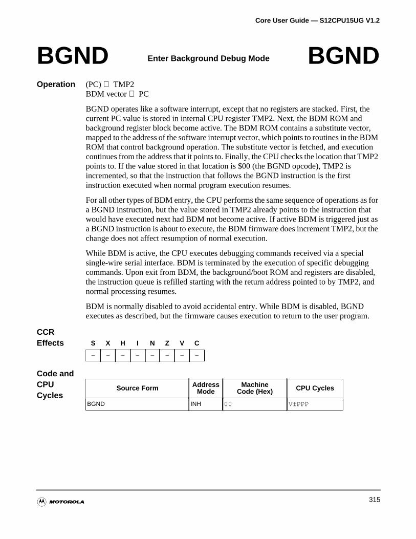
Core User Guide — S12CPU15UG V1.2
the
tor,DMtionMP2
as foratt asthe
lgled,and
ram.
Operation (PC)⇒ TMP2BDM vector⇒ PC
BGND operates like a software interrupt, except that no registers are stacked. First,current PC value is stored in internal CPU register TMP2. Next, the BDM ROM andbackground register block become active. The BDM ROM contains a substitute vecmapped to the address of the software interrupt vector, which points to routines in the BROM that control background operation. The substitute vector is fetched, and execucontinues from the address that it points to. Finally, the CPU checks the location that Tpoints to. If the value stored in that location is $00 (the BGND opcode), TMP2 isincremented, so that the instruction that follows the BGND instruction is the firstinstruction executed when normal program execution resumes.
For all other types of BDM entry, the CPU performs the same sequence of operationsa BGND instruction, but the value stored in TMP2 already points to the instruction thwould have executed next had BDM not become active. If active BDM is triggered jusa BGND instruction is about to execute, the BDM firmware does increment TMP2, butchange does not affect resumption of normal execution.
While BDM is active, the CPU executes debugging commands received via a speciasingle-wire serial interface. BDM is terminated by the execution of specific debuggincommands. Upon exit from BDM, the background/boot ROM and registers are disabthe instruction queue is refilled starting with the return address pointed to by TMP2, normal processing resumes.
BDM is normally disabled to avoid accidental entry. While BDM is disabled, BGNDexecutes as described, but the firmware causes execution to return to the user prog
CCREffects
Code andCPUCycles
BGND Enter Background Debug Mode BGND
S X H I N Z V C
– – – – – – – –
Source Form AddressMode
MachineCode (Hex) CPU Cycles
BGND INH 00 VfPPP
315
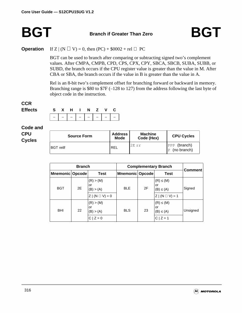
Core User Guide — S12CPU15UG V1.2
trfter
y. of
Operation If Z | (N ⊕ V) = 0, then (PC) + $0002 + rel⇒ PC
BGT can be used to branch after comparing or subtracting signed two’s complemenvalues. After CMPA, CMPB, CPD, CPS, CPX, CPY, SBCA, SBCB, SUBA, SUBB, oSUBD, the branch occurs if the CPU register value is greater than the value in M. ACBA or SBA, the branch occurs if the value in B is greater than the value in A.
Rel is an 8-bit two’s complement offset for branching forward or backward in memorBranching range is $80 to $7F (–128 to 127) from the address following the last byteobject code in the instruction.
CCREffects
Code andCPUCycles
BGT Branch if Greater Than Zero BGT
S X H I N Z V C
– – – – – – – –
Source Form AddressMode
MachineCode (Hex) CPU Cycles
BGT rel8 REL2E rr PPP (branch)
P (no branch)
Branch Complementary BranchComment
Mnemonic Opcode Test Mnemonic Opcode Test
BGT 2E
(R) > (M)or(B) > (A) BLE 2F
(R) ≤ (M)or(B) ≤ (A) Signed
Z | (N ⊕ V) = 0 Z | (N ⊕ V) = 1
BHI 22
(R) > (M)or(B) > (A) BLS 23
(R) ≤ (M)or(B) ≤ (A) Unsigned
C | Z = 0 C | Z = 1
316
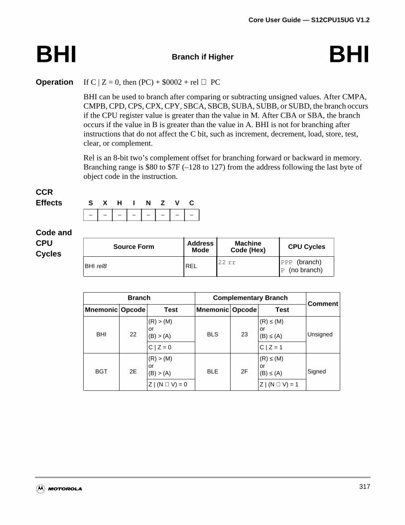
Core User Guide — S12CPU15UG V1.2
PA,ursh
est,
y. of
Operation If C | Z = 0, then (PC) + $0002 + rel⇒ PC
BHI can be used to branch after comparing or subtracting unsigned values. After CMCMPB, CPD, CPS, CPX, CPY, SBCA, SBCB, SUBA, SUBB, or SUBD, the branch occif the CPU register value is greater than the value in M. After CBA or SBA, the brancoccurs if the value in B is greater than the value in A. BHI is not for branching afterinstructions that do not affect the C bit, such as increment, decrement, load, store, tclear, or complement.
Rel is an 8-bit two’s complement offset for branching forward or backward in memorBranching range is $80 to $7F (–128 to 127) from the address following the last byteobject code in the instruction.
CCREffects
Code andCPUCycles
BHI Branch if Higher BHI
S X H I N Z V C
– – – – – – – –
Source Form AddressMode
MachineCode (Hex) CPU Cycles
BHI rel8 REL22 rr PPP (branch)
P (no branch)
Branch Complementary BranchComment
Mnemonic Opcode Test Mnemonic Opcode Test
BHI 22
(R) > (M)or(B) > (A) BLS 23
(R) ≤ (M)or(B) ≤ (A) Unsigned
C | Z = 0 C | Z = 1
BGT 2E
(R) > (M)or(B) > (A) BLE 2F
(R) ≤ (M)or(B) ≤ (A) Signed
Z | (N ⊕ V) = 0 Z | (N ⊕ V) = 1
317
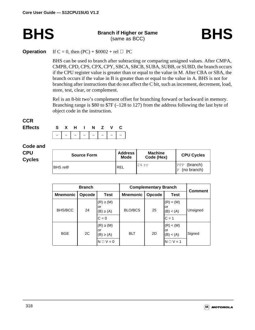
Core User Guide — S12CPU15UG V1.2
PA,urstheforload,
y. of
Operation If C = 0, then (PC) + $0002 + rel⇒ PC
BHS can be used to branch after subtracting or comparing unsigned values. After CMCMPB, CPD, CPS, CPX, CPY, SBCA, SBCB, SUBA, SUBB, or SUBD, the branch occif the CPU register value is greater than or equal to the value in M. After CBA or SBA,branch occurs if the value in B is greater than or equal to the value in A. BHS is not branching after instructions that do not affect the C bit, such as increment, decrement,store, test, clear, or complement.
Rel is an 8-bit two’s complement offset for branching forward or backward in memorBranching range is $80 to $7F (–128 to 127) from the address following the last byteobject code in the instruction.
CCREffects
Code andCPUCycles
BHS Branch if Higher or Same(same as BCC) BHS
S X H I N Z V C
– – – – – – – –
Source Form AddressMode
MachineCode (Hex) CPU Cycles
BHS rel8 REL24 rr PPP (branch)
P (no branch)
Branch Complementary BranchComment
Mnemonic Opcode Test Mnemonic Opcode Test
BHS/BCC 24
(R) ≥ (M)or(B) ≥ (A) BLO/BCS 25
(R) < (M)or(B) < (A) Unsigned
C = 0 C = 1
BGE 2C
(R) ≥ (M)or(B) ≥ (A) BLT 2D
(R) < (M)or(B) < (A) Signed
N ⊕ V = 0 N ⊕ V = 1
318
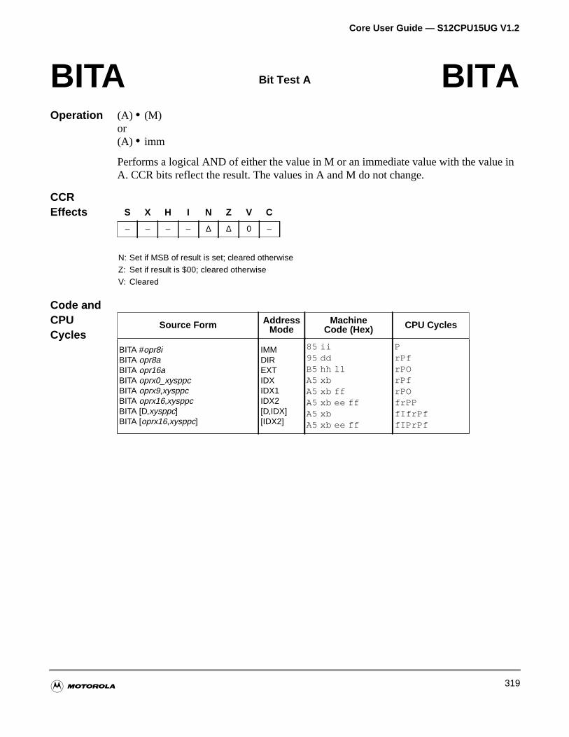
Core User Guide — S12CPU15UG V1.2
in
Operation (A) • (M)or(A) • imm
Performs a logical AND of either the value in M or an immediate value with the valueA. CCR bits reflect the result. The values in A and M do not change.
CCREffects
Code andCPUCycles
BITA Bit Test A BITA
S X H I N Z V C
– – – – ∆ ∆ 0 –
N: Set if MSB of result is set; cleared otherwiseZ: Set if result is $00; cleared otherwiseV: Cleared
Source Form AddressMode
MachineCode (Hex) CPU Cycles
BITA #opr8iBITA opr8aBITA opr16aBITA oprx0_xysppcBITA oprx9,xysppcBITA oprx16,xysppcBITA [D,xysppc]BITA [oprx16,xysppc]
IMMDIREXTIDXIDX1IDX2[D,IDX][IDX2]
85 ii95 ddB5 hh llA5 xbA5 xb ffA5 xb ee ffA5 xbA5 xb ee ff
PrPfrPOrPfrPOfrPPfIfrPffIPrPf
319
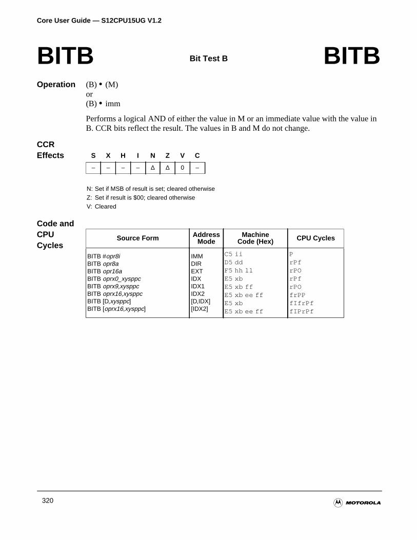
Core User Guide — S12CPU15UG V1.2
in
Operation (B) • (M)or(B) • imm
Performs a logical AND of either the value in M or an immediate value with the valueB. CCR bits reflect the result. The values in B and M do not change.
CCREffects
Code andCPUCycles
BITB Bit Test B BITB
S X H I N Z V C
– – – – ∆ ∆ 0 –
N: Set if MSB of result is set; cleared otherwiseZ: Set if result is $00; cleared otherwiseV: Cleared
Source Form AddressMode
MachineCode (Hex) CPU Cycles
BITB #opr8iBITB opr8aBITB opr16aBITB oprx0_xysppcBITB oprx9,xysppcBITB oprx16,xysppcBITB [D,xysppc]BITB [oprx16,xysppc]
IMMDIREXTIDXIDX1IDX2[D,IDX][IDX2]
C5 iiD5 ddF5 hh llE5 xbE5 xb ffE5 xb ee ffE5 xbE5 xb ee ff
PrPfrPOrPfrPOfrPPfIfrPffIPrPf
320
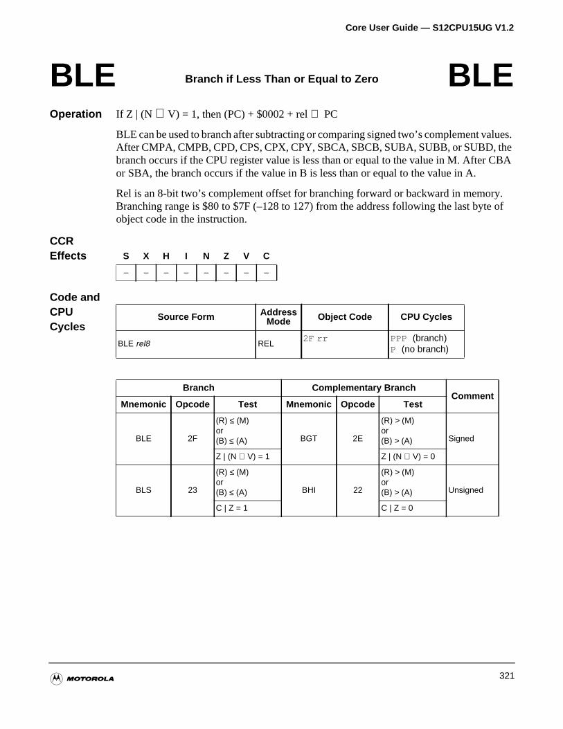
Core User Guide — S12CPU15UG V1.2
lues.eBA
y. of
Operation If Z | (N ⊕ V) = 1, then (PC) + $0002 + rel⇒ PC
BLE can be used to branch after subtracting or comparing signed two’s complement vaAfter CMPA, CMPB, CPD, CPS, CPX, CPY, SBCA, SBCB, SUBA, SUBB, or SUBD, thbranch occurs if the CPU register value is less than or equal to the value in M. After Cor SBA, the branch occurs if the value in B is less than or equal to the value in A.
Rel is an 8-bit two’s complement offset for branching forward or backward in memorBranching range is $80 to $7F (–128 to 127) from the address following the last byteobject code in the instruction.
CCREffects
Code andCPUCycles
BLE Branch if Less Than or Equal to Zero BLE
S X H I N Z V C
– – – – – – – –
Source Form AddressMode Object Code CPU Cycles
BLE rel8 REL2F rr PPP (branch)
P (no branch)
Branch Complementary BranchComment
Mnemonic Opcode Test Mnemonic Opcode Test
BLE 2F
(R) ≤ (M)or(B) ≤ (A) BGT 2E
(R) > (M)or(B) > (A) Signed
Z | (N ⊕ V) = 1 Z | (N ⊕ V) = 0
BLS 23
(R) ≤ (M)or(B) ≤ (A) BHI 22
(R) > (M)or(B) > (A) Unsigned
C | Z = 1 C | Z = 0
321
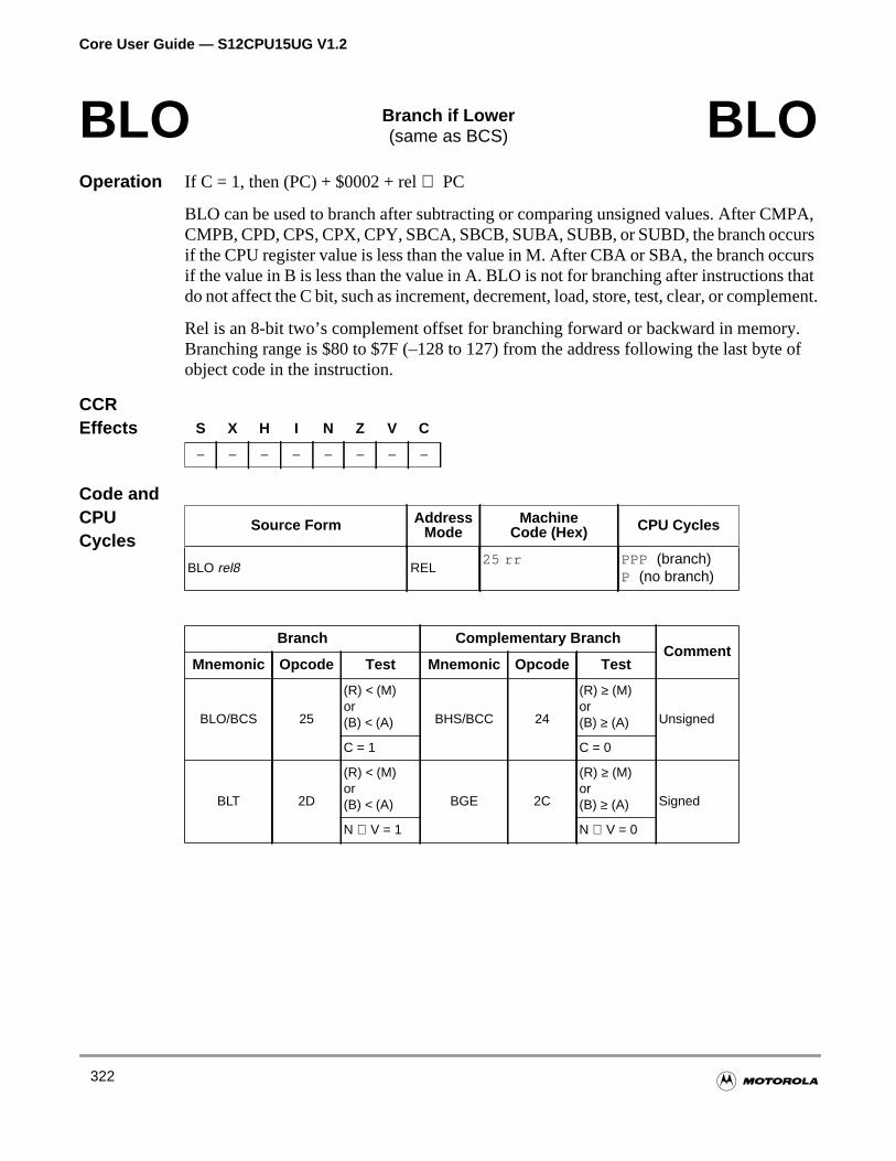
Core User Guide — S12CPU15UG V1.2
PA,ursurshatment.
y. of
Operation If C = 1, then (PC) + $0002 + rel⇒ PC
BLO can be used to branch after subtracting or comparing unsigned values. After CMCMPB, CPD, CPS, CPX, CPY, SBCA, SBCB, SUBA, SUBB, or SUBD, the branch occif the CPU register value is less than the value in M. After CBA or SBA, the branch occif the value in B is less than the value in A. BLO is not for branching after instructions tdo not affect the C bit, such as increment, decrement, load, store, test, clear, or comple
Rel is an 8-bit two’s complement offset for branching forward or backward in memorBranching range is $80 to $7F (–128 to 127) from the address following the last byteobject code in the instruction.
CCREffects
Code andCPUCycles
BLO Branch if Lower(same as BCS) BLO
S X H I N Z V C
– – – – – – – –
Source Form AddressMode
MachineCode (Hex) CPU Cycles
BLO rel8 REL25 rr PPP (branch)
P (no branch)
Branch Complementary BranchComment
Mnemonic Opcode Test Mnemonic Opcode Test
BLO/BCS 25
(R) < (M)or(B) < (A) BHS/BCC 24
(R) ≥ (M)or(B) ≥ (A) Unsigned
C = 1 C = 0
BLT 2D
(R) < (M)or(B) < (A) BGE 2C
(R) ≥ (M)or(B) ≥ (A) Signed
N ⊕ V = 1 N ⊕ V = 0
322

Core User Guide — S12CPU15UG V1.2
MPA,urshe
load,
y. of
Operation If C | Z = 1, then (PC) + $0002 + rel⇒ PC
BLS can be used to branch after subtracting or comparing unsigned values. After CCMPB, CPD, CPS, CPX, CPY, SBCA, SBCB, SUBA, SUBB, or SUBD, the branch occif the CPU register value is less than or equal to the value in M. After CBA or SBA, tbranch occurs if the value in B is less than or equal to the value in A. BLS is not forbranching after instructions that do not affect the C bit, such as increment, decrement,store, test, clear, or complement.
Rel is an 8-bit two’s complement offset for branching forward or backward in memorBranching range is $80 to $7F (–128 to 127) from the address following the last byteobject code in the instruction.
CCREffects
Code andCPUCycles
BLS Branch if Lower or Same BLS
S X H I N Z V C
– – – – – – – –
Source Form AddressMode
MachineCode (Hex) CPU Cycles
BLS rel8 REL23 rr PPP (branch)
P (no branch)
Branch Complementary BranchComment
Mnemonic Opcode Test Mnemonic Opcode Test
BLS 23
(R) ≤ (M)or(B) ≤ (A) BHI 22
(R) > (M)or(B) > (A) Unsigned
C | Z = 1 C | Z = 0
BLE 2F
(R) ≤ (M)or(B) ≤ (A) BGT 2E
(R) > (M)or(B) > (A) Signed
Z | (N ⊕ V) = 1 Z | (N ⊕ V) = 0
323
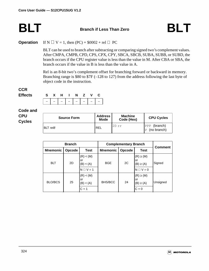
Core User Guide — S12CPU15UG V1.2
lues.ethe
y. of
Operation If N ⊕ V = 1, then (PC) + $0002 + rel⇒ PC
BLT can be used to branch after subtracting or comparing signed two’s complement vaAfter CMPA, CMPB, CPD, CPS, CPX, CPY, SBCA, SBCB, SUBA, SUBB, or SUBD, thbranch occurs if the CPU register value is less than the value in M. After CBA or SBA,branch occurs if the value in B is less than the value in A.
Rel is an 8-bit two’s complement offset for branching forward or backward in memorBranching range is $80 to $7F (–128 to 127) from the address following the last byteobject code in the instruction.
CCREffects
Code andCPUCycles
BLT Branch if Less Than Zero BLT
S X H I N Z V C
– – – – – – – –
Source Form AddressMode
MachineCode (Hex) CPU Cycles
BLT rel8 REL2D rr PPP (branch)
P (no branch)
Branch Complementary BranchComment
Mnemonic Opcode Test Mnemonic Opcode Test
BLT 2D
(R) < (M)or(B) < (A) BGE 2C
(R) ≥ (M)or(B) ≥ (A) Signed
N ⊕ V = 1 N ⊕ V = 0
BLO/BCS 25
(R) < (M)or(B) < (A) BHS/BCC 24
(R) ≥ (M)or(B) ≥ (A) Unsigned
C = 1 C = 0
324
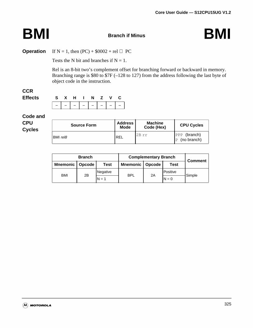
Core User Guide — S12CPU15UG V1.2
y. of
Operation If N = 1, then (PC) + $0002 + rel⇒ PC
Tests the N bit and branches if N = 1.
Rel is an 8-bit two’s complement offset for branching forward or backward in memorBranching range is $80 to $7F (–128 to 127) from the address following the last byteobject code in the instruction.
CCREffects
Code andCPUCycles
BMI Branch if Minus BMI
S X H I N Z V C
– – – – – – – –
Source Form AddressMode
MachineCode (Hex) CPU Cycles
BMI rel8 REL2B rr PPP (branch)
P (no branch)
Branch Complementary BranchComment
Mnemonic Opcode Test Mnemonic Opcode Test
BMI 2BNegative
BPL 2APositive
SimpleN = 1 N = 0
325
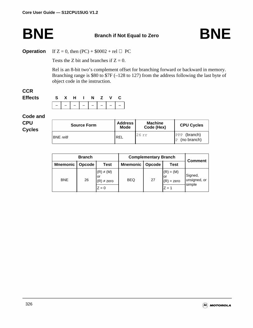
Core User Guide — S12CPU15UG V1.2
y. of
Operation If Z = 0, then (PC) + $0002 + rel⇒ PC
Tests the Z bit and branches if Z = 0.
Rel is an 8-bit two’s complement offset for branching forward or backward in memorBranching range is $80 to $7F (–128 to 127) from the address following the last byteobject code in the instruction.
CCREffects
Code andCPUCycles
BNE Branch if Not Equal to Zero BNE
S X H I N Z V C
– – – – – – – –
Source Form AddressMode
MachineCode (Hex) CPU Cycles
BNE rel8 REL26 rr PPP (branch)
P (no branch)
Branch Complementary BranchComment
Mnemonic Opcode Test Mnemonic Opcode Test
BNE 26
(R) ≠ (M)or(R) ≠ zero BEQ 27
(R) = (M)or(R) = zero
Signed,unsigned, orsimple
Z = 0 Z = 1
326
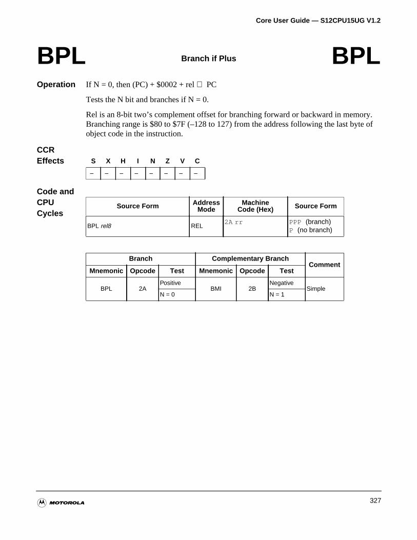
Core User Guide — S12CPU15UG V1.2
y. of
Operation If N = 0, then (PC) + $0002 + rel⇒ PC
Tests the N bit and branches if N = 0.
Rel is an 8-bit two’s complement offset for branching forward or backward in memorBranching range is $80 to $7F (–128 to 127) from the address following the last byteobject code in the instruction.
CCREffects
Code andCPUCycles
BPL Branch if Plus BPL
S X H I N Z V C
– – – – – – – –
Source Form AddressMode
MachineCode (Hex) Source Form
BPL rel8 REL2A rr PPP (branch)
P (no branch)
Branch Complementary BranchComment
Mnemonic Opcode Test Mnemonic Opcode Test
BPL 2APositive
BMI 2BNegative
SimpleN = 0 N = 1
327
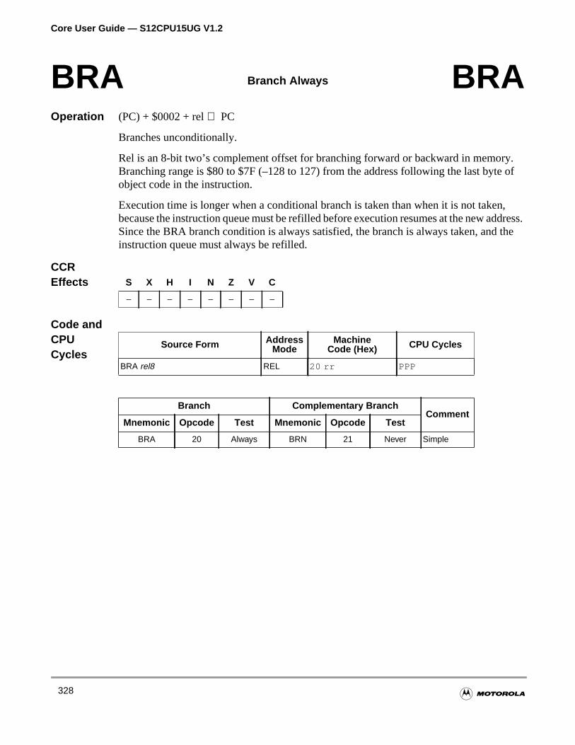
Core User Guide — S12CPU15UG V1.2
y. of
,dress.
the
Operation (PC) + $0002 + rel⇒ PC
Branches unconditionally.
Rel is an 8-bit two’s complement offset for branching forward or backward in memorBranching range is $80 to $7F (–128 to 127) from the address following the last byteobject code in the instruction.
Execution time is longer when a conditional branch is taken than when it is not takenbecause the instruction queue must be refilled before execution resumes at the new adSince the BRA branch condition is always satisfied, the branch is always taken, andinstruction queue must always be refilled.
CCREffects
Code andCPUCycles
BRA Branch Always BRA
S X H I N Z V C
– – – – – – – –
Source Form AddressMode
MachineCode (Hex) CPU Cycles
BRA rel8 REL 20 rr PPP
Branch Complementary BranchComment
Mnemonic Opcode Test Mnemonic Opcode Test
BRA 20 Always BRN 21 Never Simple
328
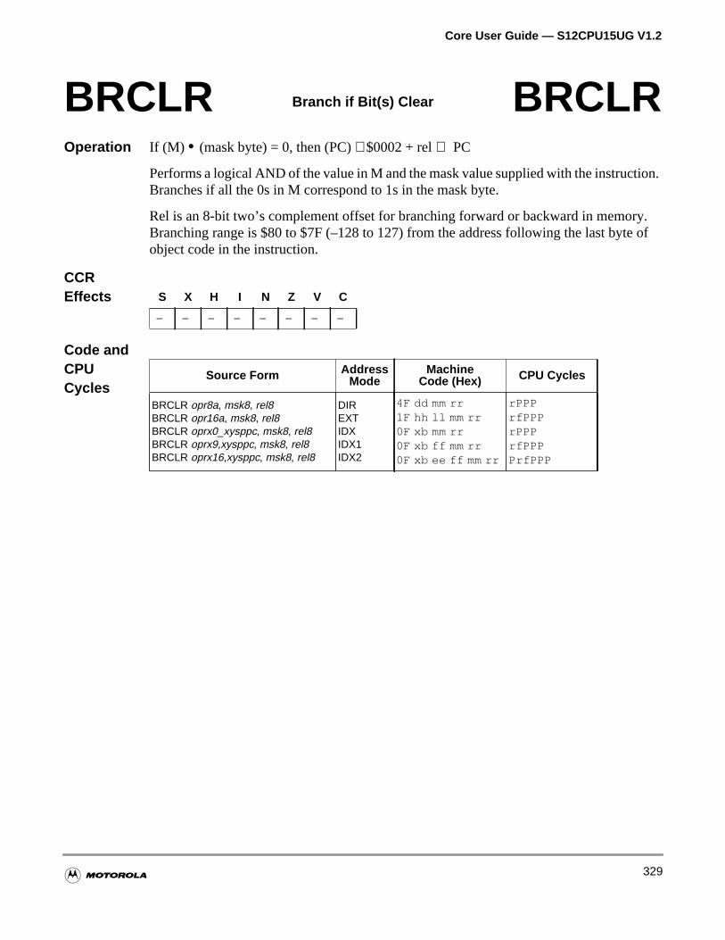
Core User Guide — S12CPU15UG V1.2
ion.
y. of
Operation If (M) • (mask byte) = 0, then (PC)+ $0002 + rel⇒ PC
Performs a logical AND of the value in M and the mask value supplied with the instructBranches if all the 0s in M correspond to 1s in the mask byte.
Rel is an 8-bit two’s complement offset for branching forward or backward in memorBranching range is $80 to $7F (–128 to 127) from the address following the last byteobject code in the instruction.
CCREffects
Code andCPUCycles
BRCLR Branch if Bit(s) Clear BRCLR
S X H I N Z V C
– – – – – – – –
Source Form AddressMode
MachineCode (Hex) CPU Cycles
BRCLR opr8a, msk8, rel8BRCLR opr16a, msk8, rel8BRCLR oprx0_xysppc, msk8, rel8BRCLR oprx9,xysppc, msk8, rel8BRCLR oprx16,xysppc, msk8, rel8
DIREXTIDXIDX1IDX2
4F dd mm rr1F hh ll mm rr0F xb mm rr0F xb ff mm rr0F xb ee ff mm rr
rPPPrfPPPrPPPrfPPPPrfPPP
329
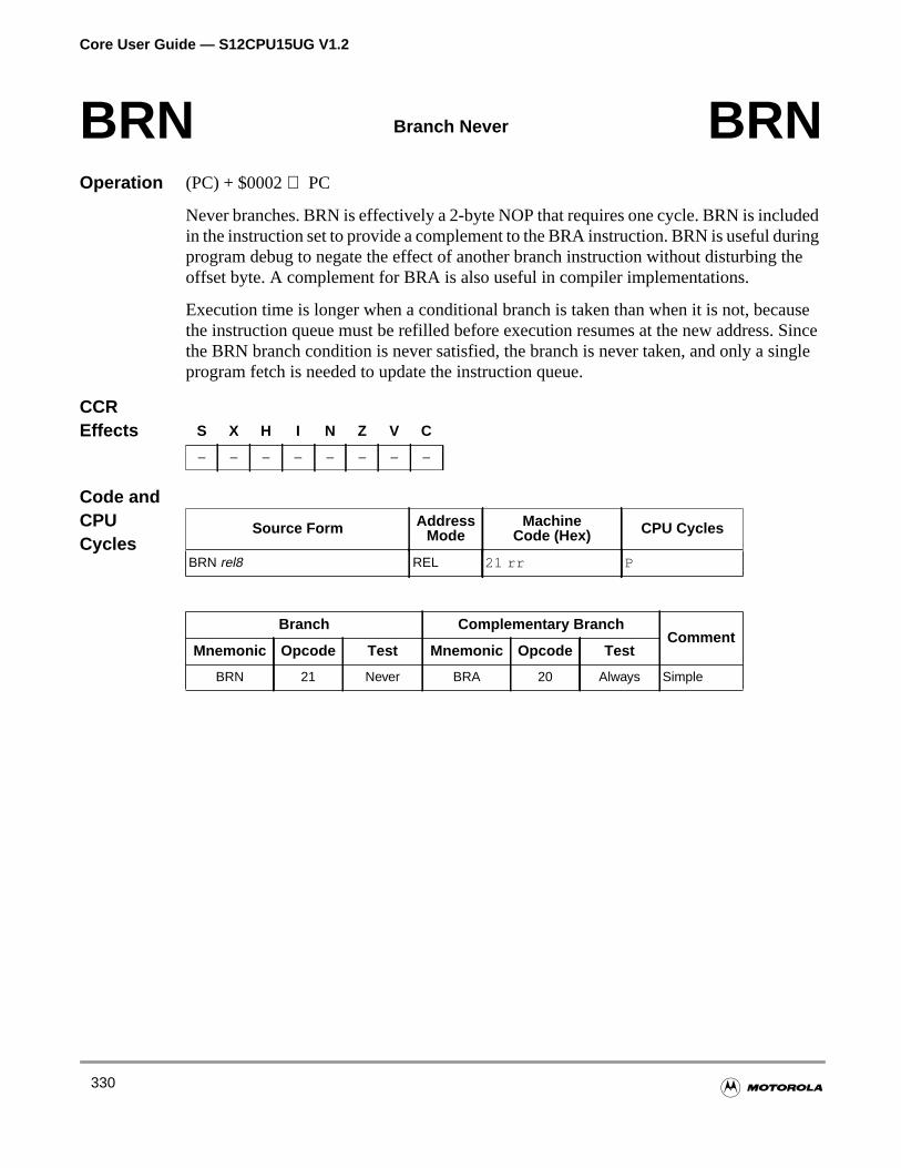
Core User Guide — S12CPU15UG V1.2
dedingthe
use. Sinceingle
Operation (PC) + $0002⇒ PC
Never branches. BRN is effectively a 2-byte NOP that requires one cycle. BRN is incluin the instruction set to provide a complement to the BRA instruction. BRN is useful durprogram debug to negate the effect of another branch instruction without disturbing offset byte. A complement for BRA is also useful in compiler implementations.
Execution time is longer when a conditional branch is taken than when it is not, becathe instruction queue must be refilled before execution resumes at the new addressthe BRN branch condition is never satisfied, the branch is never taken, and only a sprogram fetch is needed to update the instruction queue.
CCREffects
Code andCPUCycles
BRN Branch Never BRN
S X H I N Z V C
– – – – – – – –
Source Form AddressMode
MachineCode (Hex) CPU Cycles
BRN rel8 REL 21 rr P
Branch Complementary BranchComment
Mnemonic Opcode Test Mnemonic Opcode Test
BRN 21 Never BRA 20 Always Simple
330
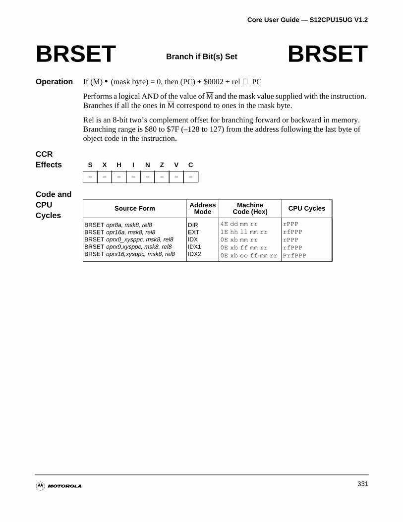
Core User Guide — S12CPU15UG V1.2
.
y. of
Operation If (M) • (mask byte) = 0, then (PC) + $0002 + rel⇒ PC
Performs a logical AND of the value ofM and the mask value supplied with the instructionBranches if all the ones inM correspond to ones in the mask byte.
Rel is an 8-bit two’s complement offset for branching forward or backward in memorBranching range is $80 to $7F (–128 to 127) from the address following the last byteobject code in the instruction.
CCREffects
Code andCPUCycles
BRSET Branch if Bit(s) Set BRSET
S X H I N Z V C
– – – – – – – –
Source Form AddressMode
MachineCode (Hex) CPU Cycles
BRSET opr8a, msk8, rel8BRSET opr16a, msk8, rel8BRSET oprx0_xysppc, msk8, rel8BRSET oprx9,xysppc, msk8, rel8BRSET oprx16,xysppc, msk8, rel8
DIREXTIDXIDX1IDX2
4E dd mm rr1E hh ll mm rr0E xb mm rr0E xb ff mm rr0E xb ee ff mm rr
rPPPrfPPPrPPPrfPPPPrfPPP
331
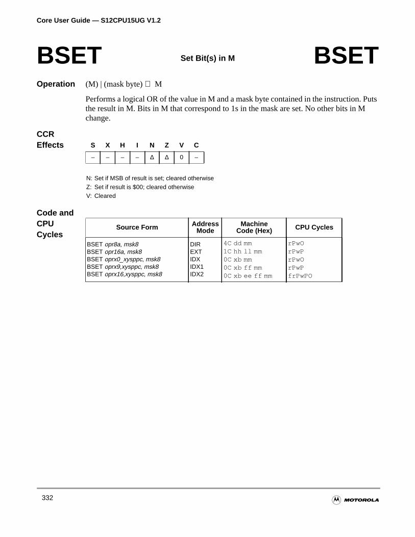
Core User Guide — S12CPU15UG V1.2
Puts
Operation (M) | (mask byte)⇒ M
Performs a logical OR of the value in M and a mask byte contained in the instruction.the result in M. Bits in M that correspond to 1s in the mask are set. No other bits in Mchange.
CCREffects
Code andCPUCycles
BSET Set Bit(s) in M BSET
S X H I N Z V C
– – – – ∆ ∆ 0 –
N: Set if MSB of result is set; cleared otherwiseZ: Set if result is $00; cleared otherwiseV: Cleared
Source Form AddressMode
MachineCode (Hex) CPU Cycles
BSET opr8a, msk8BSET opr16a, msk8BSET oprx0_xysppc, msk8BSET oprx9,xysppc, msk8BSET oprx16,xysppc, msk8
DIREXTIDXIDX1IDX2
4C dd mm1C hh ll mm0C xb mm0C xb ff mm0C xb ee ff mm
rPwOrPwPrPwOrPwPfrPwPO
332
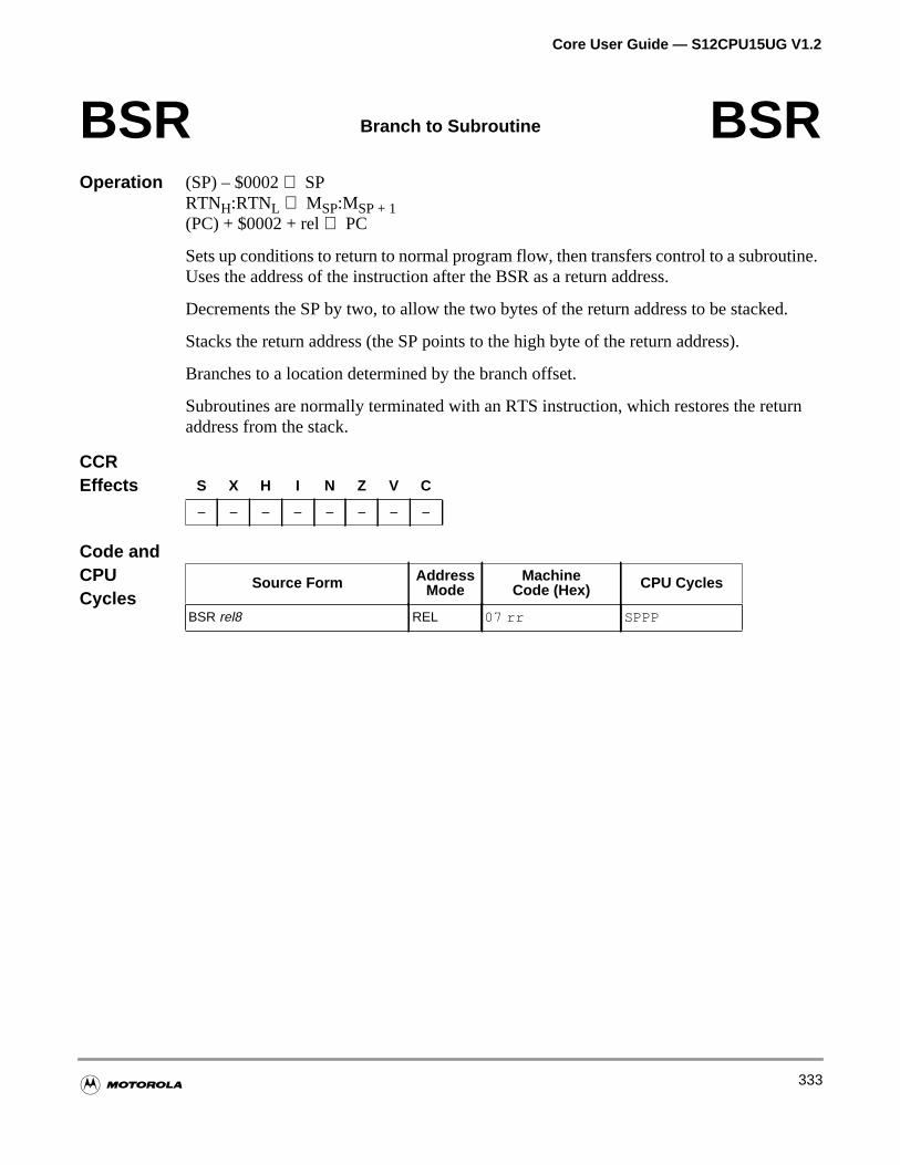
Core User Guide — S12CPU15UG V1.2
tine.
d.
urn
Operation (SP) – $0002⇒ SPRTNH:RTNL ⇒ MSP:MSP + 1(PC) + $0002 + rel⇒ PC
Sets up conditions to return to normal program flow, then transfers control to a subrouUses the address of the instruction after the BSR as a return address.
Decrements the SP by two, to allow the two bytes of the return address to be stacke
Stacks the return address (the SP points to the high byte of the return address).
Branches to a location determined by the branch offset.
Subroutines are normally terminated with an RTS instruction, which restores the retaddress from the stack.
CCREffects
Code andCPUCycles
BSR Branch to Subroutine BSR
S X H I N Z V C
– – – – – – – –
Source Form AddressMode
MachineCode (Hex) CPU Cycles
BSR rel8 REL 07 rr SPPP
333
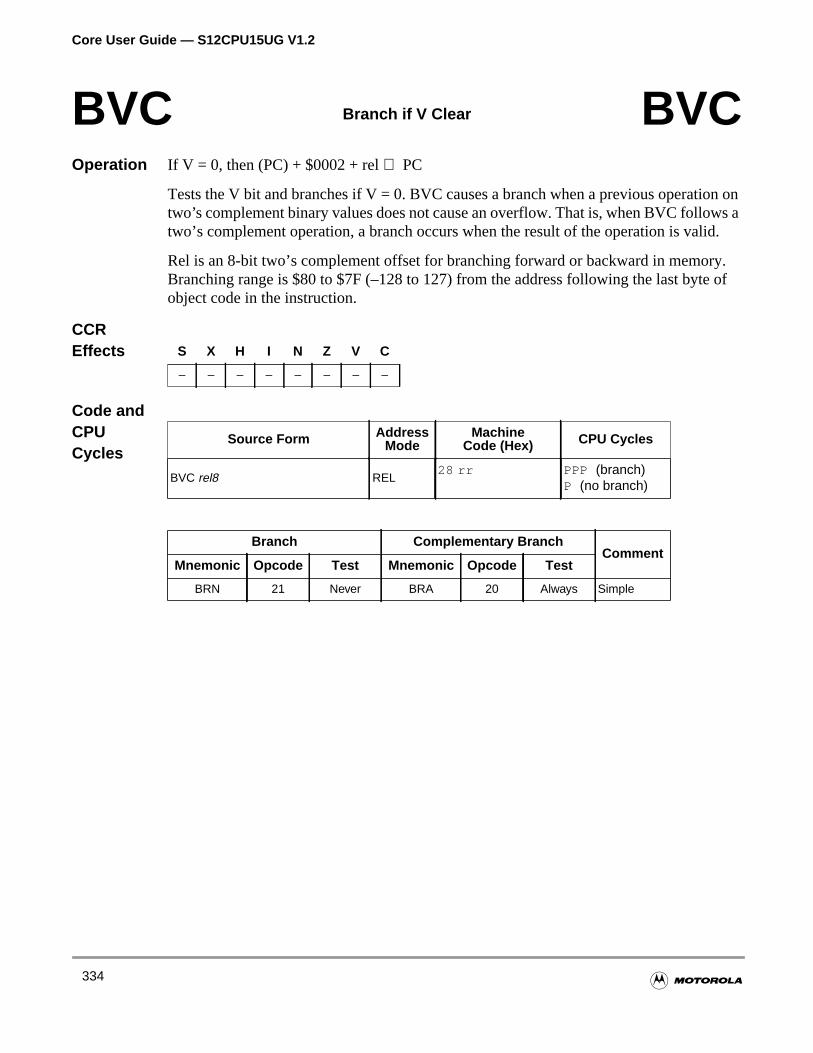
Core User Guide — S12CPU15UG V1.2
n ons a
id.
y. of
Operation If V = 0, then (PC) + $0002 + rel⇒ PC
Tests the V bit and branches if V = 0. BVC causes a branch when a previous operatiotwo’s complement binary values does not cause an overflow. That is, when BVC followtwo’s complement operation, a branch occurs when the result of the operation is val
Rel is an 8-bit two’s complement offset for branching forward or backward in memorBranching range is $80 to $7F (–128 to 127) from the address following the last byteobject code in the instruction.
CCREffects
Code andCPUCycles
BVC Branch if V Clear BVC
S X H I N Z V C
– – – – – – – –
Source Form AddressMode
MachineCode (Hex) CPU Cycles
BVC rel8 REL28 rr PPP (branch)
P (no branch)
Branch Complementary BranchComment
Mnemonic Opcode Test Mnemonic Opcode Test
BRN 21 Never BRA 20 Always Simple
334
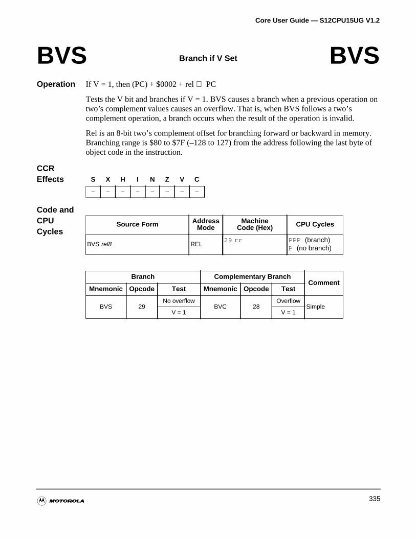
Core User Guide — S12CPU15UG V1.2
on
y. of
Operation If V = 1, then (PC) + $0002 + rel⇒ PC
Tests the V bit and branches if V = 1. BVS causes a branch when a previous operationtwo’s complement values causes an overflow. That is, when BVS follows a two’scomplement operation, a branch occurs when the result of the operation is invalid.
Rel is an 8-bit two’s complement offset for branching forward or backward in memorBranching range is $80 to $7F (–128 to 127) from the address following the last byteobject code in the instruction.
CCREffects
Code andCPUCycles
BVS Branch if V Set BVS
S X H I N Z V C
– – – – – – – –
Source Form AddressMode
MachineCode (Hex) CPU Cycles
BVS rel8 REL29 rr PPP (branch)
P (no branch)
Branch Complementary BranchComment
Mnemonic Opcode Test Mnemonic Opcode Test
BVS 29No overflow
BVC 28Overflow
SimpleV = 1 V = 1
335
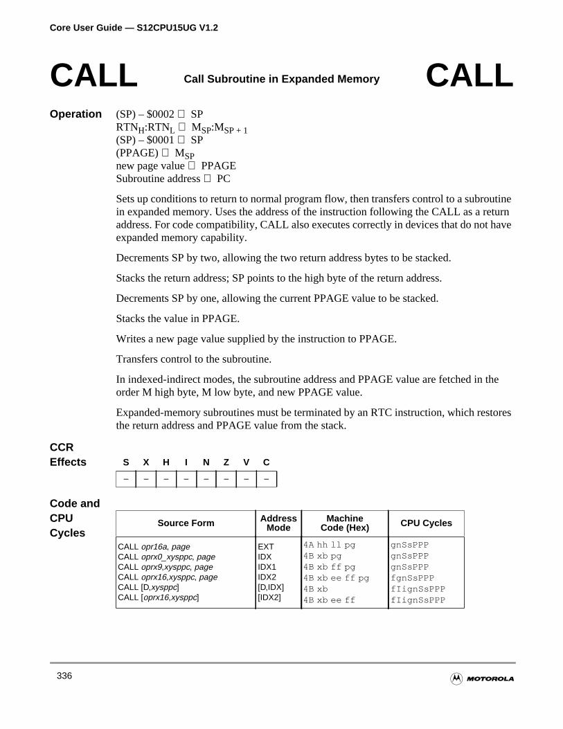
Core User Guide — S12CPU15UG V1.2
tineturnave
the
tores
Operation (SP) – $0002⇒ SPRTNH:RTNL ⇒ MSP:MSP + 1(SP) – $0001⇒ SP(PPAGE)⇒ MSPnew page value⇒ PPAGESubroutine address⇒ PC
Sets up conditions to return to normal program flow, then transfers control to a subrouin expanded memory. Uses the address of the instruction following the CALL as a readdress. For code compatibility, CALL also executes correctly in devices that do not hexpanded memory capability.
Decrements SP by two, allowing the two return address bytes to be stacked.
Stacks the return address; SP points to the high byte of the return address.
Decrements SP by one, allowing the current PPAGE value to be stacked.
Stacks the value in PPAGE.
Writes a new page value supplied by the instruction to PPAGE.
Transfers control to the subroutine.
In indexed-indirect modes, the subroutine address and PPAGE value are fetched inorder M high byte, M low byte, and new PPAGE value.
Expanded-memory subroutines must be terminated by an RTC instruction, which resthe return address and PPAGE value from the stack.
CCREffects
Code andCPUCycles
CALL Call Subroutine in Expanded Memory CALL
S X H I N Z V C
– – – – – – – –
Source Form AddressMode
MachineCode (Hex) CPU Cycles
CALL opr16a, pageCALL oprx0_xysppc, pageCALL oprx9,xysppc, pageCALL oprx16,xysppc, pageCALL [D,xysppc]CALL [oprx16,xysppc]
EXTIDXIDX1IDX2[D,IDX][IDX2]
4A hh ll pg4B xb pg4B xb ff pg4B xb ee ff pg4B xb4B xb ee ff
gnSsPPPgnSsPPPgnSsPPPfgnSsPPPfIignSsPPPfIignSsPPP
336
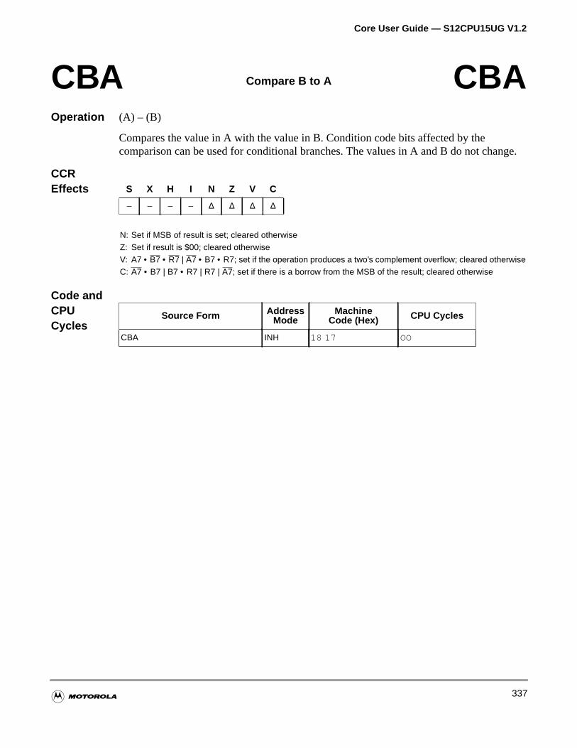
Core User Guide — S12CPU15UG V1.2
nge.
Operation (A) – (B)
Compares the value in A with the value in B. Condition code bits affected by thecomparison can be used for conditional branches. The values in A and B do not cha
CCREffects
Code andCPUCycles
CBA Compare B to A CBA
S X H I N Z V C
– – – – ∆ ∆ ∆ ∆
N: Set if MSB of result is set; cleared otherwiseZ: Set if result is $00; cleared otherwiseV: A7 • B7 • R7 | A7 • B7 • R7; set if the operation produces a two’s complement overflow; cleared otherwiseC: A7 • B7 | B7 • R7 | R7 | A7; set if there is a borrow from the MSB of the result; cleared otherwise
Source Form AddressMode
MachineCode (Hex) CPU Cycles
CBA INH 18 17 OO
337

Core User Guide — S12CPU15UG V1.2
bit.
Operation 0 ⇒ C bit
Clears the C bit. CLC assembles as ANDCC #$FE.
CLC can be used to initialize the C bit prior to a shift or rotate instruction affecting the C
CCREffects
Code andCPUCycles
CLC Clear C(same as ANDCC #$FE) CLC
S X H I N Z V C
– – – – – – – 0
C: Cleared
Source Form AddressMode
MachineCode (Hex) CPU Cycles
CLC IMM 10 FE P
338
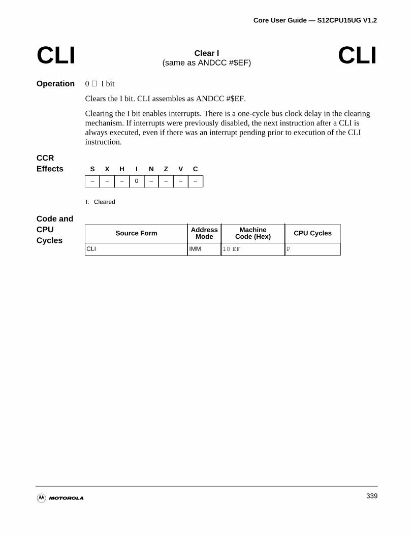
Core User Guide — S12CPU15UG V1.2
ring
I
Operation 0 ⇒ I bit
Clears the I bit. CLI assembles as ANDCC #$EF.
Clearing the I bit enables interrupts. There is a one-cycle bus clock delay in the cleamechanism. If interrupts were previously disabled, the next instruction after a CLI isalways executed, even if there was an interrupt pending prior to execution of the CLinstruction.
CCREffects
Code andCPUCycles
CLI Clear I(same as ANDCC #$EF) CLI
S X H I N Z V C
– – – 0 – – – –
I: Cleared
Source Form AddressMode
MachineCode (Hex) CPU Cycles
CLI IMM 10 EF P
339
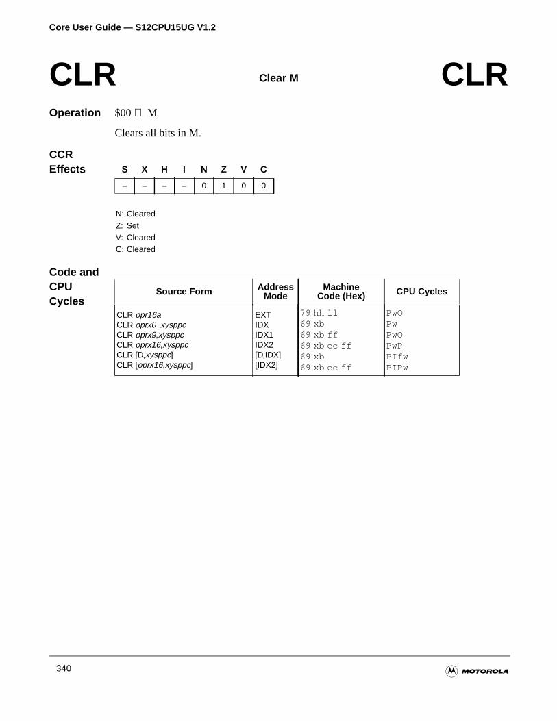
Core User Guide — S12CPU15UG V1.2
Operation $00⇒ M
Clears all bits in M.
CCREffects
Code andCPUCycles
CLR Clear M CLR
S X H I N Z V C
– – – – 0 1 0 0
N: ClearedZ: SetV: ClearedC: Cleared
Source Form AddressMode
MachineCode (Hex) CPU Cycles
CLR opr16aCLR oprx0_xysppcCLR oprx9,xysppcCLR oprx16,xysppcCLR [D,xysppc]CLR [oprx16,xysppc]
EXTIDXIDX1IDX2[D,IDX][IDX2]
79 hh ll69 xb69 xb ff69 xb ee ff69 xb69 xb ee ff
PwOPwPwOPwPPIfwPIPw
340
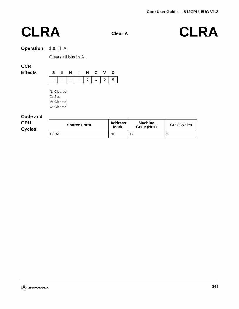
Core User Guide — S12CPU15UG V1.2
Operation $00⇒ A
Clears all bits in A.
CCREffects
Code andCPUCycles
CLRA Clear A CLRA
S X H I N Z V C
– – – – 0 1 0 0
N: ClearedZ: SetV: ClearedC: Cleared
Source Form AddressMode
MachineCode (Hex) CPU Cycles
CLRA INH 87 O
341
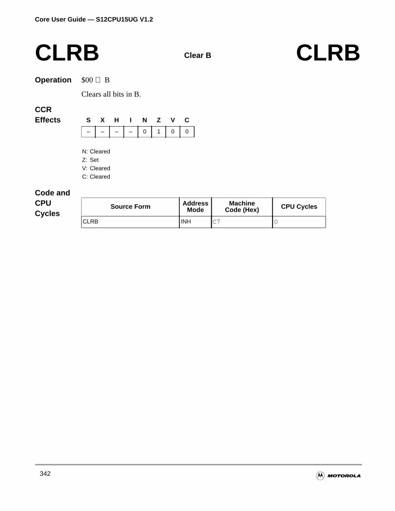
Core User Guide — S12CPU15UG V1.2
Operation $00⇒ B
Clears all bits in B.
CCREffects
Code andCPUCycles
CLRB Clear B CLRB
S X H I N Z V C
– – – – 0 1 0 0
N: ClearedZ: SetV: ClearedC: Cleared
Source Form AddressMode
MachineCode (Hex) CPU Cycles
CLRB INH C7 O
342
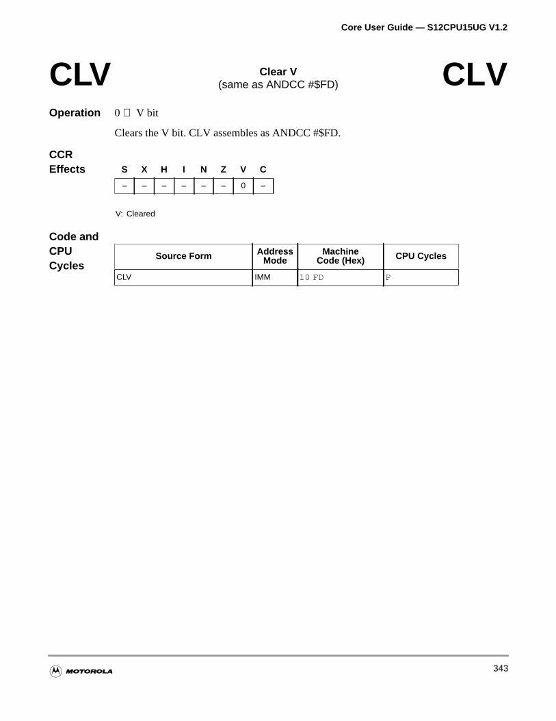
Core User Guide — S12CPU15UG V1.2
Operation 0 ⇒ V bit
Clears the V bit. CLV assembles as ANDCC #$FD.
CCREffects
Code andCPUCycles
CLV Clear V(same as ANDCC #$FD) CLV
S X H I N Z V C
– – – – – – 0 –
V: Cleared
Source Form AddressMode
MachineCode (Hex) CPU Cycles
CLV IMM 10 FD P
343

Core User Guide — S12CPU15UG V1.2
flect
Operation (A) – (M)or(A) – imm
Compares the value in A to either the value in M or an immediate value. CCR bits rethe result. The values in A and M do not change.
CCREffects
Code andCPUCycles
CMPA Compare A CMPA
S X H I N Z V C
– – – – ∆ ∆ ∆ ∆
N: Set if MSB of result is set; cleared otherwiseZ: Set if result is $00; cleared otherwiseV: A7 • M7 • R7 | A7 • M7 • R7; set if the operation produces a two’s complement overflow; cleared
otherwiseC: A7 • M7 | M7 • R7 | R7 • A7; set if there is a borrow from the MSB of the result; cleared otherwise
Source Form AddressMode
MachineCode (Hex) CPU Cycles
CMPA #opr8iCMPA opr8aCMPA opr16aCMPA oprx0_xysppcCMPA oprx9,xysppcCMPA oprx16,xysppcCMPA [D,xysppc]CMPA [oprx16,xysppc]
IMMDIREXTIDXIDX1IDX2[D,IDX][IDX2]
81 ii91 ddB1 hh llA1 xbA1 xb ffA1 xb ee ffA1 xbA1 xb ee ff
PrPfrPOrPfrPOfrPPfIfrPffIPrPf
344
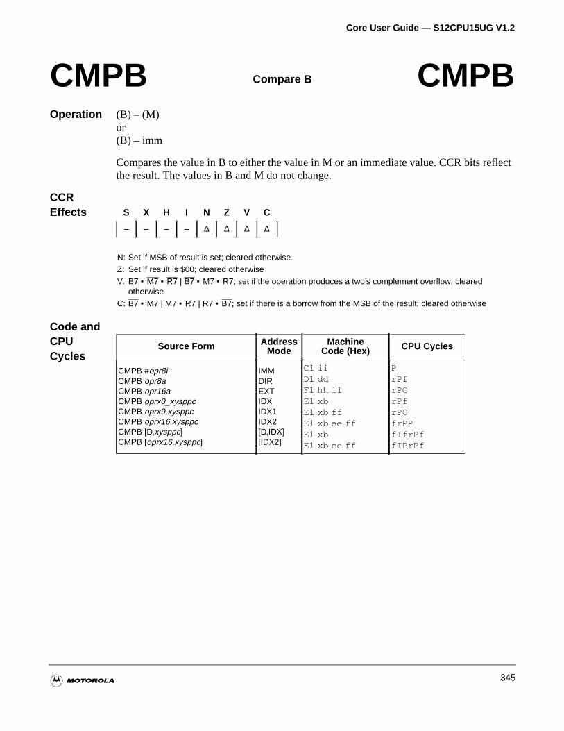
Core User Guide — S12CPU15UG V1.2
flect
Operation (B) – (M)or(B) – imm
Compares the value in B to either the value in M or an immediate value. CCR bits rethe result. The values in B and M do not change.
CCREffects
Code andCPUCycles
CMPB Compare B CMPB
S X H I N Z V C
– – – – ∆ ∆ ∆ ∆
N: Set if MSB of result is set; cleared otherwiseZ: Set if result is $00; cleared otherwiseV: B7 • M7 • R7 | B7 • M7 • R7; set if the operation produces a two’s complement overflow; cleared
otherwiseC: B7 • M7 | M7 • R7 | R7 • B7; set if there is a borrow from the MSB of the result; cleared otherwise
Source Form AddressMode
MachineCode (Hex) CPU Cycles
CMPB #opr8iCMPB opr8aCMPB opr16aCMPB oprx0_xysppcCMPB oprx9,xysppcCMPB oprx16,xysppcCMPB [D,xysppc]CMPB [oprx16,xysppc]
IMMDIREXTIDXIDX1IDX2[D,IDX][IDX2]
C1 iiD1 ddF1 hh llE1 xbE1 xb ffE1 xb ee ffE1 xbE1 xb ee ff
PrPfrPOrPfrPOfrPPfIfrPffIPrPf
345
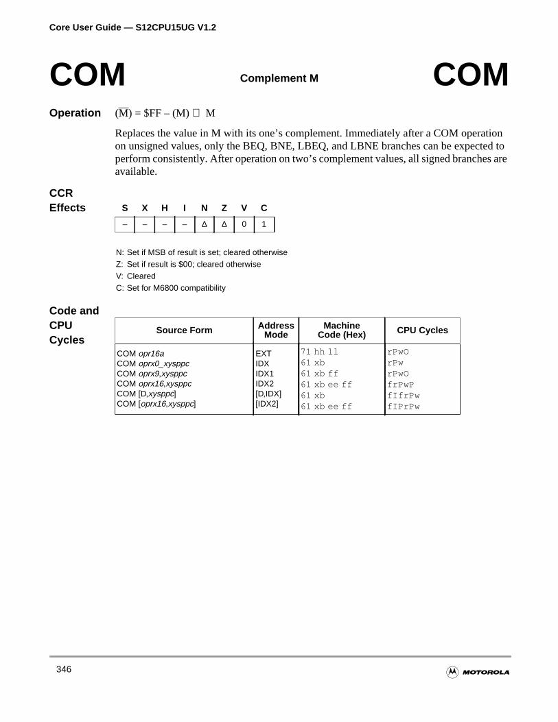
Core User Guide — S12CPU15UG V1.2
tioned tos are
Operation (M) = $FF – (M)⇒ M
Replaces the value in M with its one’s complement. Immediately after a COM operaon unsigned values, only the BEQ, BNE, LBEQ, and LBNE branches can be expectperform consistently. After operation on two’s complement values, all signed brancheavailable.
CCREffects
Code andCPUCycles
COM Complement M COM
S X H I N Z V C
– – – – ∆ ∆ 0 1
N: Set if MSB of result is set; cleared otherwiseZ: Set if result is $00; cleared otherwiseV: ClearedC: Set for M6800 compatibility
Source Form AddressMode
MachineCode (Hex) CPU Cycles
COM opr16aCOM oprx0_xysppcCOM oprx9,xysppcCOM oprx16,xysppcCOM [D,xysppc]COM [oprx16,xysppc]
EXTIDXIDX1IDX2[D,IDX][IDX2]
71 hh ll61 xb61 xb ff61 xb ee ff61 xb61 xb ee ff
rPwOrPwrPwOfrPwPfIfrPwfIPrPw
346
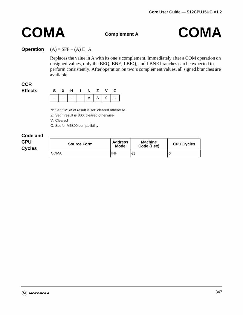
Core User Guide — S12CPU15UG V1.2
n ontos are
Operation (A) = $FF – (A)⇒ A
Replaces the value in A with its one’s complement. Immediately after a COM operatiounsigned values, only the BEQ, BNE, LBEQ, and LBNE branches can be expected perform consistently. After operation on two’s complement values, all signed brancheavailable.
CCREffects
Code andCPUCycles
COMA Complement A COMA
S X H I N Z V C
– – – – ∆ ∆ 0 1
N: Set if MSB of result is set; cleared otherwiseZ: Set if result is $00; cleared otherwiseV: ClearedC: Set for M6800 compatibility
Source Form AddressMode
MachineCode (Hex) CPU Cycles
COMA INH 41 O
347
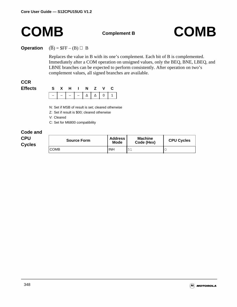
Core User Guide — S12CPU15UG V1.2
and
Operation (B) = $FF – (B)⇒ B
Replaces the value in B with its one’s complement. Each bit of B is complemented.Immediately after a COM operation on unsigned values, only the BEQ, BNE, LBEQ,LBNE branches can be expected to perform consistently. After operation on two’scomplement values, all signed branches are available.
CCREffects
Code andCPUCycles
COMB Complement B COMB
S X H I N Z V C
– – – – ∆ ∆ 0 1
N: Set if MSB of result is set; cleared otherwiseZ: Set if result is $00; cleared otherwiseV: ClearedC: Set for M6800 compatibility
Source Form AddressMode
MachineCode (Hex) CPU Cycles
COMB INH 51 O
348

Core User Guide — S12CPU15UG V1.2
bits
Operation (A):(B) – (M):(M + 1)or(A:B) – imm
Compares the value in D to either the value in M:M + 1 or an immediate value. CCRreflect the result. The values in D and M:M + 1 do not change.
CCREffects
Code andCPUCycles
CPD Compare D CPD
S X H I N Z V C
– – – – ∆ ∆ ∆ ∆
N: Set if MSB of result is set; cleared otherwiseZ: Set if result is $0000; cleared otherwiseV: D15 • M15 • R15 | D15 • M15 • R15; set if the operation produces a two’s complement overflow; cleared
otherwiseC: D15 • M15 | M15 • R15 | R15 • D15; set if the absolute value of (M:M + 1) is larger than the absolute value
of (D); cleared otherwise
Source Form AddressMode
MachineCode (Hex) CPU Cycles
CPD #opr16iCPD opr8aCPD opr16aCPD oprx0_xysppcCPD oprx9,xysppcCPD oprx16,xysppcCPD [D,xysppc]CPD [oprx16,xysppc]
IMMDIREXTIDXIDX1IDX2[D,IDX][IDX2]
8C jj kk9C ddBC hh llAC xbAC xb ffAC xb ee ffAC xbAC xb ee ff
PORPfRPORPfRPOfRPPfIfRPffIPRPf
349
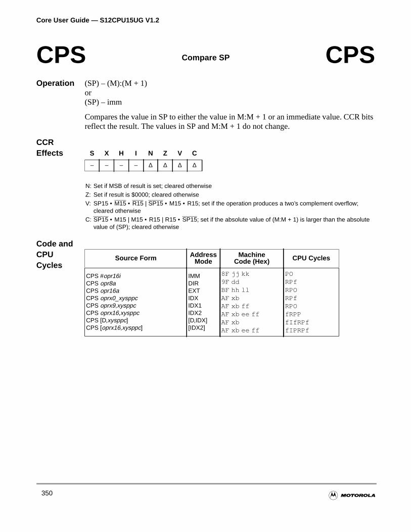
Core User Guide — S12CPU15UG V1.2
bits
Operation (SP) – (M):(M + 1)or(SP) – imm
Compares the value in SP to either the value in M:M + 1 or an immediate value. CCRreflect the result. The values in SP and M:M + 1 do not change.
CCREffects
Code andCPUCycles
CPS Compare SP CPS
S X H I N Z V C
– – – – ∆ ∆ ∆ ∆
N: Set if MSB of result is set; cleared otherwiseZ: Set if result is $0000; cleared otherwiseV: SP15 • M15 • R15 | SP15 • M15 • R15; set if the operation produces a two’s complement overflow;
cleared otherwiseC: SP15 • M15 | M15 • R15 | R15 • SP15; set if the absolute value of (M:M + 1) is larger than the absolute
value of (SP); cleared otherwise
Source Form AddressMode
MachineCode (Hex) CPU Cycles
CPS #opr16iCPS opr8aCPS opr16aCPS oprx0_xysppcCPS oprx9,xysppcCPS oprx16,xysppcCPS [D,xysppc]CPS [oprx16,xysppc]
IMMDIREXTIDXIDX1IDX2[D,IDX][IDX2]
8F jj kk9F ddBF hh llAF xbAF xb ffAF xb ee ffAF xbAF xb ee ff
PORPfRPORPfRPOfRPPfIfRPffIPRPf
350
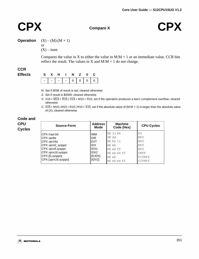
Core User Guide — S12CPU15UG V1.2
bits
Operation (X) – (M):(M + 1)or(X) – imm
Compares the value in X to either the value in M:M + 1 or an immediate value. CCRreflect the result. The values in X and M:M + 1 do not change.
CCREffects
Code andCPUCycles
CPX Compare X CPX
S X H I N Z V C
– – – – ∆ ∆ ∆ ∆
N: Set if MSB of result is set; cleared otherwiseZ: Set if result is $0000; cleared otherwiseV: X15 • M15 • R15 | X15 • M15 • R15; set if the operation produces a two’s complement overflow; cleared
otherwiseC: X15 • M15 | M15 • R15 | R15 • X15; set if the absolute value of (M:M + 1) is larger than the absolute value
of (X); cleared otherwise
Source Form AddressMode
MachineCode (Hex) CPU Cycles
CPX #opr16iCPX opr8aCPX opr16aCPX oprx0_xysppcCPX oprx9,xysppcCPX oprx16,xysppcCPX [D,xysppc]CPX [oprx16,xysppc]
IMMDIREXTIDXIDX1IDX2[D,IDX][IDX2]
8E jj kk9E ddBE hh llAE xbAE xb ffAE xb ee ffAE xbAE xb ee ff
PORPfRPORPfRPOfRPPfIfRPffIPRPf
351
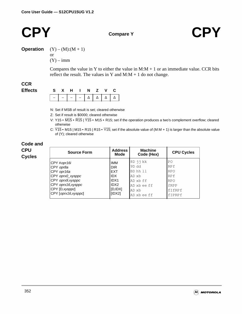
Core User Guide — S12CPU15UG V1.2
bits
Operation (Y) – (M):(M + 1)or(Y) – imm
Compares the value in Y to either the value in M:M + 1 or an immediate value. CCRreflect the result. The values in Y and M:M + 1 do not change.
CCREffects
Code andCPUCycles
CPY Compare Y CPY
S X H I N Z V C
– – – – ∆ ∆ ∆ ∆
N: Set if MSB of result is set; cleared otherwiseZ: Set if result is $0000; cleared otherwiseV: Y15 • M15 • R15 | Y15 • M15 • R15; set if the operation produces a two’s complement overflow; cleared
otherwiseC: Y15 • M15 | M15 • R15 | R15 • Y15; set if the absolute value of (M:M + 1) is larger than the absolute value
of (Y); cleared otherwise
Source Form AddressMode
MachineCode (Hex) CPU Cycles
CPY #opr16iCPY opr8aCPY opr16aCPY oprx0_xysppcCPY oprx9,xysppcCPY oprx16,xysppcCPY [D,xysppc]CPY [oprx16,xysppc]
IMMDIREXTIDXIDX1IDX2[D,IDX][IDX2]
8D jj kk9D ddBD hh llAD xbAD xb ffAD xb ee ffAD xbAD xb ee ff
PORPfRPORPfRPOfRPPfIfRPffIPRPf
352
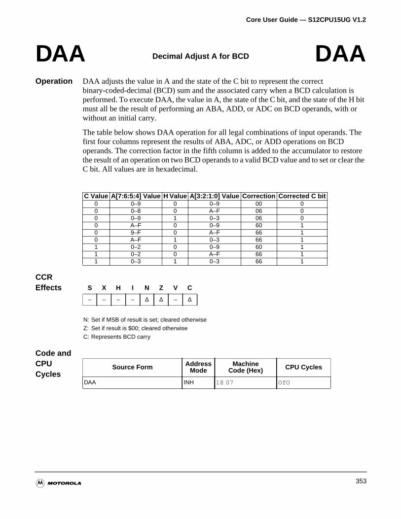
Core User Guide — S12CPU15UG V1.2
isbit
r
The
storer the
Operation DAA adjusts the value in A and the state of the C bit to represent the correctbinary-coded-decimal (BCD) sum and the associated carry when a BCD calculationperformed. To execute DAA, the value in A, the state of the C bit, and the state of the Hmust all be the result of performing an ABA, ADD, or ADC on BCD operands, with owithout an initial carry.
The table below shows DAA operation for all legal combinations of input operands. first four columns represent the results of ABA, ADC, or ADD operations on BCDoperands. The correction factor in the fifth column is added to the accumulator to rethe result of an operation on two BCD operands to a valid BCD value and to set or cleaC bit. All values are in hexadecimal.
CCREffects
Code andCPUCycles
DAA Decimal Adjust A for BCD DAA
C Value A[7:6:5:4] Value H Value A[3:2:1:0] Value Correction Corrected C bit0 0–9 0 0–9 00 00 0–8 0 A–F 06 00 0–9 1 0–3 06 00 A–F 0 0–9 60 10 9–F 0 A–F 66 10 A–F 1 0–3 66 11 0–2 0 0–9 60 11 0–2 0 A–F 66 11 0–3 1 0–3 66 1
S X H I N Z V C
– – – – ∆ ∆ – ∆
N: Set if MSB of result is set; cleared otherwiseZ: Set if result is $00; cleared otherwiseC: Represents BCD carry
Source Form AddressMode
MachineCode (Hex) CPU Cycles
DAA INH 18 07 OfO
353
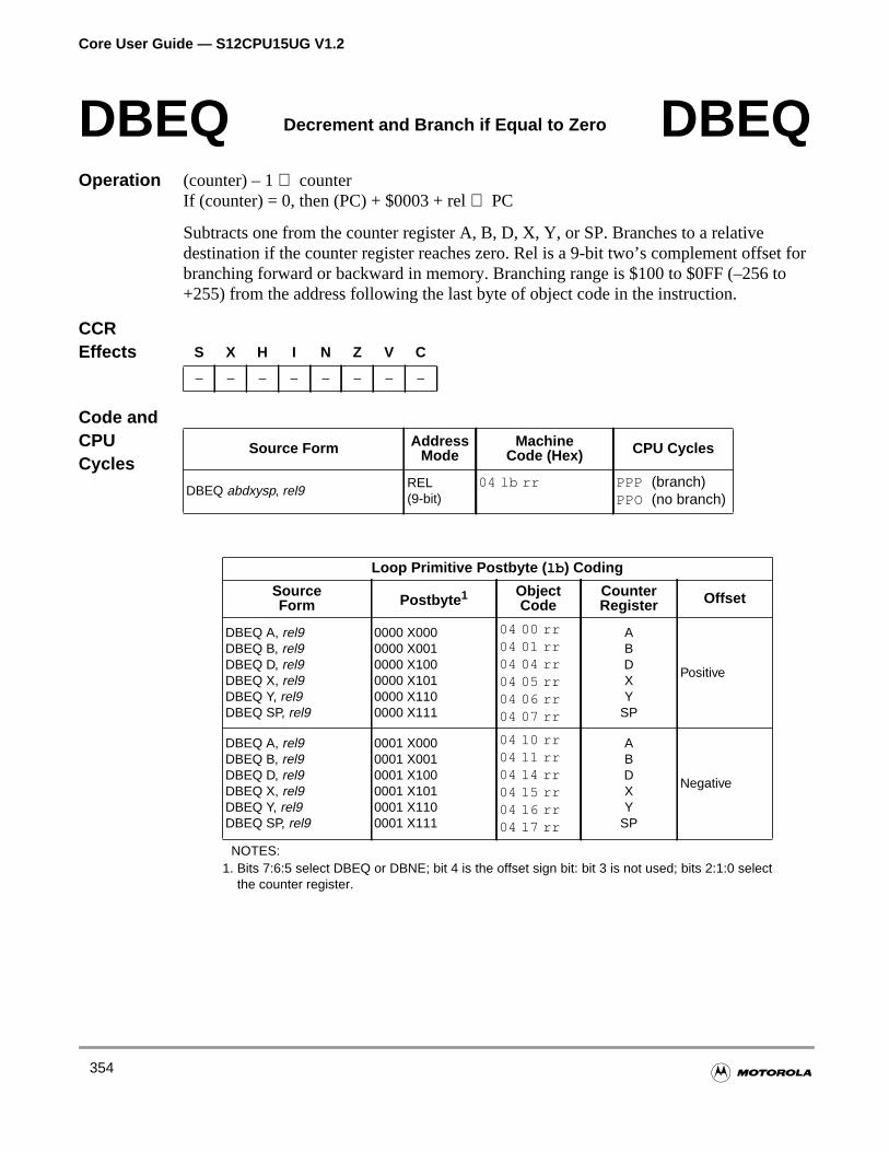
Core User Guide — S12CPU15UG V1.2
et forto
Operation (counter) – 1⇒ counterIf (counter) = 0, then (PC) + $0003 + rel⇒ PC
Subtracts one from the counter register A, B, D, X, Y, or SP. Branches to a relativedestination if the counter register reaches zero. Rel is a 9-bit two’s complement offsbranching forward or backward in memory. Branching range is $100 to $0FF (–256 +255) from the address following the last byte of object code in the instruction.
CCREffects
Code andCPUCycles
DBEQ Decrement and Branch if Equal to Zero DBEQ
S X H I N Z V C
– – – – – – – –
Source Form AddressMode
MachineCode (Hex) CPU Cycles
DBEQ abdxysp, rel9REL(9-bit)
04 lb rr PPP (branch)PPO (no branch)
Loop Primitive Postbyte ( lb ) Coding
SourceForm Postbyte 1
NOTES:1. Bits 7:6:5 select DBEQ or DBNE; bit 4 is the offset sign bit: bit 3 is not used; bits 2:1:0 select
the counter register.
ObjectCode
CounterRegister Offset
DBEQ A, rel9DBEQ B, rel9DBEQ D, rel9DBEQ X, rel9DBEQ Y, rel9DBEQ SP, rel9
0000 X0000000 X0010000 X1000000 X1010000 X1100000 X111
04 00 rr04 01 rr04 04 rr04 05 rr04 06 rr04 07 rr
ABDXY
SP
Positive
DBEQ A, rel9DBEQ B, rel9DBEQ D, rel9DBEQ X, rel9DBEQ Y, rel9DBEQ SP, rel9
0001 X0000001 X0010001 X1000001 X1010001 X1100001 X111
04 10 rr04 11 rr04 14 rr04 15 rr04 16 rr04 17 rr
ABDXY
SP
Negative
354
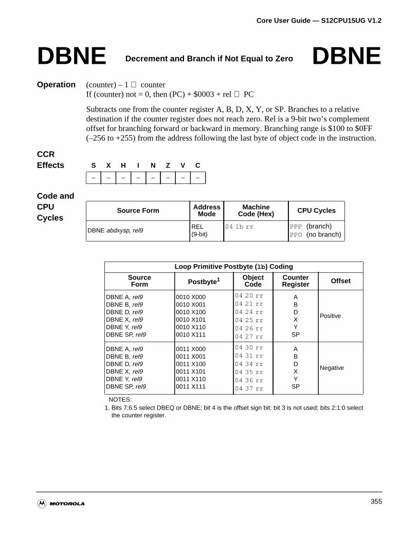
Core User Guide — S12CPU15UG V1.2
ntF
ion.
Operation (counter) – 1⇒ counterIf (counter) not = 0, then (PC) + $0003 + rel⇒ PC
Subtracts one from the counter register A, B, D, X, Y, or SP. Branches to a relativedestination if the counter register does not reach zero. Rel is a 9-bit two’s complemeoffset for branching forward or backward in memory. Branching range is $100 to $0F(–256 to +255) from the address following the last byte of object code in the instruct
CCREffects
Code andCPUCycles
DBNE Decrement and Branch if Not Equal to Zero DBNE
S X H I N Z V C
– – – – – – – –
Source Form AddressMode
MachineCode (Hex) CPU Cycles
DBNE abdxysp, rel9REL(9-bit)
04 lb rr PPP (branch)PPO (no branch)
Loop Primitive Postbyte ( lb ) Coding
SourceForm Postbyte 1
NOTES:1. Bits 7:6:5 select DBEQ or DBNE; bit 4 is the offset sign bit: bit 3 is not used; bits 2:1:0 select
the counter register.
ObjectCode
CounterRegister Offset
DBNE A, rel9DBNE B, rel9DBNE D, rel9DBNE X, rel9DBNE Y, rel9DBNE SP, rel9
0010 X0000010 X0010010 X1000010 X1010010 X1100010 X111
04 20 rr04 21 rr04 24 rr04 25 rr04 26 rr04 27 rr
ABDXY
SP
Positive
DBNE A, rel9DBNE B, rel9DBNE D, rel9DBNE X, rel9DBNE Y, rel9DBNE SP, rel9
0011 X0000011 X0010011 X1000011 X1010011 X1100011 X111
04 30 rr04 31 rr04 34 rr04 35 rr04 36 rr04 37 rr
ABDXY
SP
Negative
355
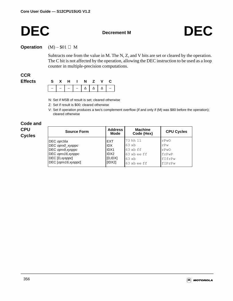
Core User Guide — S12CPU15UG V1.2
tion.loop
Operation (M) – $01⇒ M
Subtracts one from the value in M. The N, Z, and V bits are set or cleared by the operaThe C bit is not affected by the operation, allowing the DEC instruction to be used as acounter in multiple-precision computations.
CCREffects
Code andCPUCycles
DEC Decrement M DEC
S X H I N Z V C
– – – – ∆ ∆ ∆ –
N: Set if MSB of result is set; cleared otherwiseZ: Set if result is $00; cleared otherwiseV: Set if operation produces a two’s complement overflow (if and only if (M) was $80 before the operation);
cleared otherwise
Source Form AddressMode
MachineCode (Hex) CPU Cycles
DEC opr16aDEC oprx0_xysppcDEC oprx9,xysppcDEC oprx16,xysppcDEC [D,xysppc]DEC [oprx16,xysppc]
EXTIDXIDX1IDX2[D,IDX][IDX2]
73 hh ll63 xb63 xb ff63 xb ee ff63 xb63 xb ee ff
rPwOrPwrPwOfrPwPfIfrPwfIPrPw
356
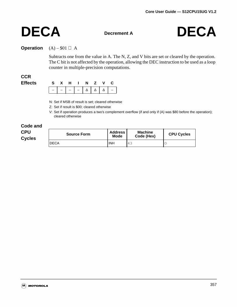
Core User Guide — S12CPU15UG V1.2
tion.loop
Operation (A) – $01⇒ A
Subtracts one from the value in A. The N, Z, and V bits are set or cleared by the operaThe C bit is not affected by the operation, allowing the DEC instruction to be used as acounter in multiple-precision computations.
CCREffects
Code andCPUCycles
DECA Decrement A DECA
S X H I N Z V C
– – – – ∆ ∆ ∆ –
N: Set if MSB of result is set; cleared otherwiseZ: Set if result is $00; cleared otherwiseV: Set if operation produces a two’s complement overflow (if and only if (A) was $80 before the operation);
cleared otherwise
Source Form AddressMode
MachineCode (Hex) CPU Cycles
DECA INH 43 O
357
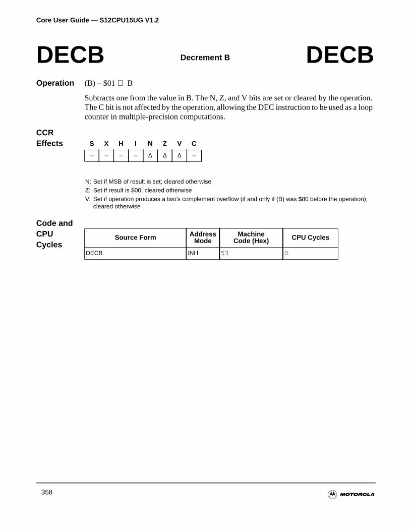
Core User Guide — S12CPU15UG V1.2
tion.loop
Operation (B) – $01⇒ B
Subtracts one from the value in B. The N, Z, and V bits are set or cleared by the operaThe C bit is not affected by the operation, allowing the DEC instruction to be used as acounter in multiple-precision computations.
CCREffects
Code andCPUCycles
DECB Decrement B DECB
S X H I N Z V C
– – – – ∆ ∆ ∆ –
N: Set if MSB of result is set; cleared otherwiseZ: Set if result is $00; cleared otherwiseV: Set if operation produces a two’s complement overflow (if and only if (B) was $80 before the operation);
cleared otherwise
Source Form AddressMode
MachineCode (Hex) CPU Cycles
DECB INH 53 O
358
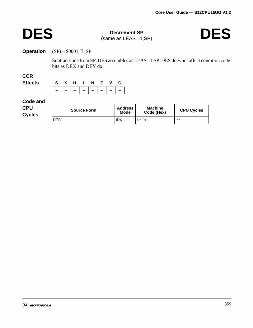
Core User Guide — S12CPU15UG V1.2
n code
Operation (SP) – $0001⇒ SP
Subtracts one from SP. DES assembles as LEAS –1,SP. DES does not affect conditiobits as DEX and DEY do.
CCREffects
Code andCPUCycles
DES Decrement SP(same as LEAS –1,SP) DES
S X H I N Z V C
– – – – – – – –
Source Form AddressMode
MachineCode (Hex) CPU Cycles
DES IDX 1B 9F Pf
359
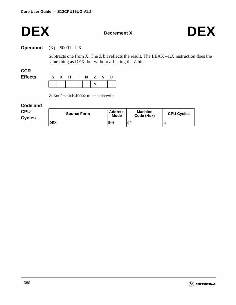
Core User Guide — S12CPU15UG V1.2
the
Operation (X) – $0001⇒ X
Subtracts one from X. The Z bit reflects the result. The LEAX –1,X instruction does same thing as DEX, but without affecting the Z bit.
CCREffects
Code andCPUCycles
DEX Decrement X DEX
S X H I N Z V C
– – – – – ∆ – –
Z: Set if result is $0000; cleared otherwise
Source Form AddressMode
MachineCode (Hex) CPU Cycles
DEX INH 09 O
360
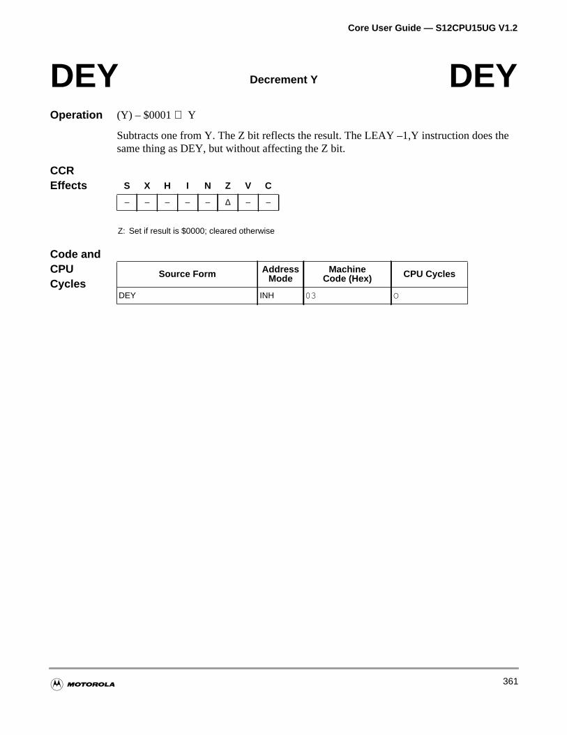
Core User Guide — S12CPU15UG V1.2
the
Operation (Y) – $0001⇒ Y
Subtracts one from Y. The Z bit reflects the result. The LEAY –1,Y instruction does same thing as DEY, but without affecting the Z bit.
CCREffects
Code andCPUCycles
DEY Decrement Y DEY
S X H I N Z V C
– – – – – ∆ – –
Z: Set if result is $0000; cleared otherwise
Source Form AddressMode
MachineCode (Hex) CPU Cycles
DEY INH 03 O
361
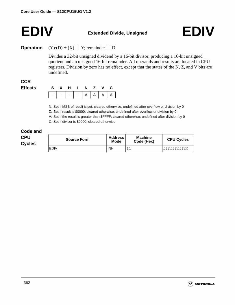
Core User Guide — S12CPU15UG V1.2
PUs are
Operation (Y):(D) ÷ (X) ⇒ Y; remainder⇒ D
Divides a 32-bit unsigned dividend by a 16-bit divisor, producing a 16-bit unsignedquotient and an unsigned 16-bit remainder. All operands and results are located in Cregisters. Division by zero has no effect, except that the states of the N, Z, and V bitundefined.
CCREffects
Code andCPUCycles
EDIV Extended Divide, Unsigned EDIV
S X H I N Z V C
– – – – ∆ ∆ ∆ ∆
N: Set if MSB of result is set; cleared otherwise; undefined after overflow or division by 0Z: Set if result is $0000; cleared otherwise; undefined after overflow or division by 0V: Set if the result is greater than $FFFF; cleared otherwise; undefined after division by 0C: Set if divisor is $0000; cleared otherwise
Source Form AddressMode
MachineCode (Hex) CPU Cycles
EDIV INH 11 ffffffffffO
362
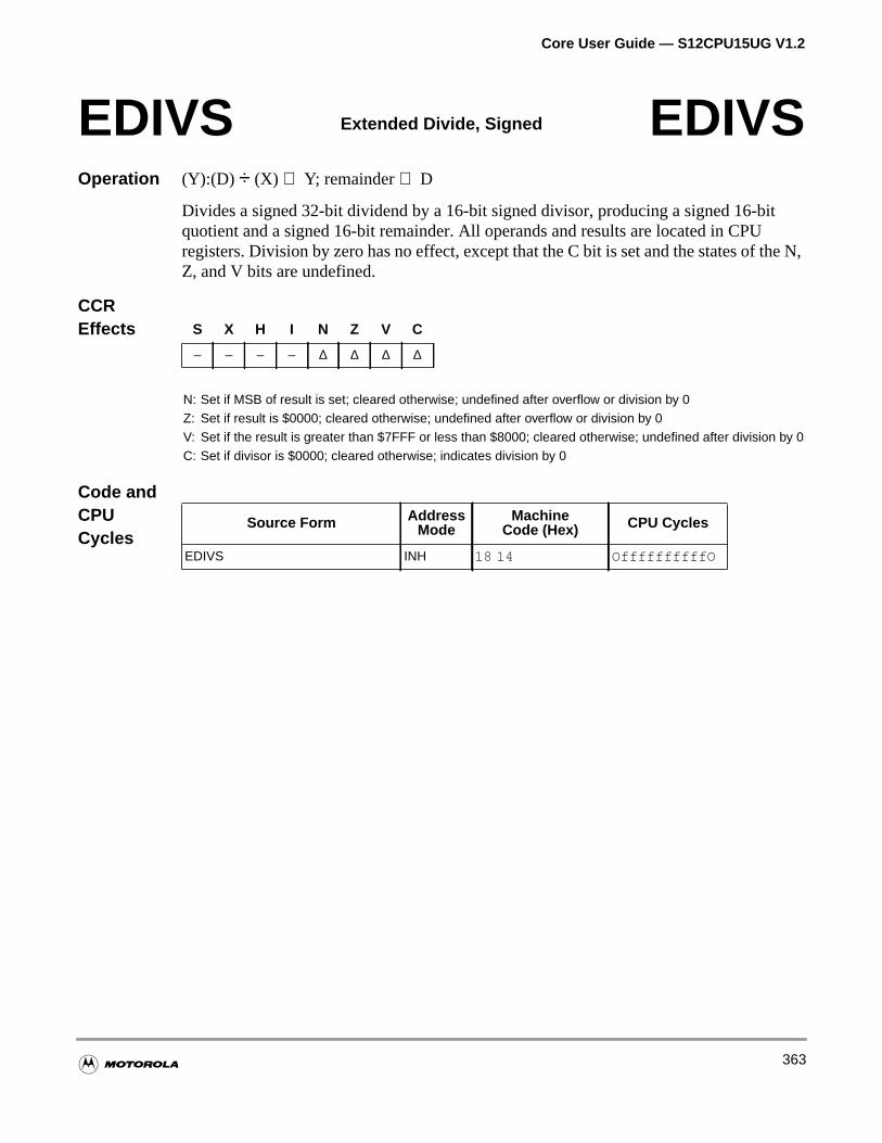
Core User Guide — S12CPU15UG V1.2
t
he N,
Operation (Y):(D) ÷ (X) ⇒ Y; remainder⇒ D
Divides a signed 32-bit dividend by a 16-bit signed divisor, producing a signed 16-biquotient and a signed 16-bit remainder. All operands and results are located in CPUregisters. Division by zero has no effect, except that the C bit is set and the states of tZ, and V bits are undefined.
CCREffects
Code andCPUCycles
EDIVS Extended Divide, Signed EDIVS
S X H I N Z V C
– – – – ∆ ∆ ∆ ∆
N: Set if MSB of result is set; cleared otherwise; undefined after overflow or division by 0Z: Set if result is $0000; cleared otherwise; undefined after overflow or division by 0V: Set if the result is greater than $7FFF or less than $8000; cleared otherwise; undefined after division by 0C: Set if divisor is $0000; cleared otherwise; indicates division by 0
Source Form AddressMode
MachineCode (Hex) CPU Cycles
EDIVS INH 18 14 OffffffffffO
363
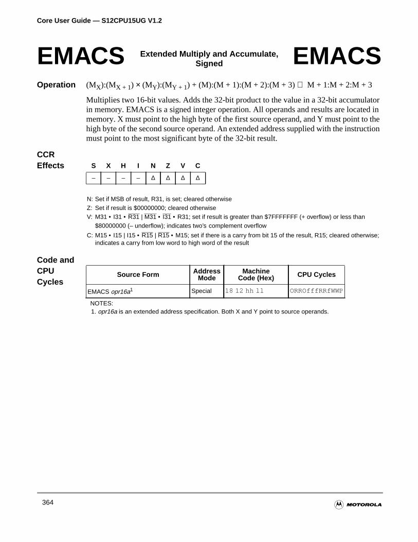
Core User Guide — S12CPU15UG V1.2
tored inthection
Operation (MX):(MX + 1) × (MY):(MY + 1) + (M):(M + 1):(M + 2):(M + 3) ⇒ M + 1:M + 2:M + 3
Multiplies two 16-bit values. Adds the 32-bit product to the value in a 32-bit accumulain memory. EMACS is a signed integer operation. All operands and results are locatmemory. X must point to the high byte of the first source operand, and Y must point tohigh byte of the second source operand. An extended address supplied with the instrumust point to the most significant byte of the 32-bit result.
CCREffects
Code andCPUCycles
EMACS Extended Multiply and Accumulate,Signed EMACS
S X H I N Z V C
– – – – ∆ ∆ ∆ ∆
N: Set if MSB of result, R31, is set; cleared otherwiseZ: Set if result is $00000000; cleared otherwiseV: M31 • I31 • R31 | M31 • I31 • R31; set if result is greater than $7FFFFFFF (+ overflow) or less than
$80000000 (– underflow); indicates two’s complement overflow
C: M15 • I15 | I15 • R15 | R15 • M15; set if there is a carry from bit 15 of the result, R15; cleared otherwise;indicates a carry from low word to high word of the result
Source Form AddressMode
MachineCode (Hex) CPU Cycles
EMACS opr16a1
NOTES:1. opr16a is an extended address specification. Both X and Y point to source operands.
Special 18 12 hh ll ORROfffRRfWWP
364
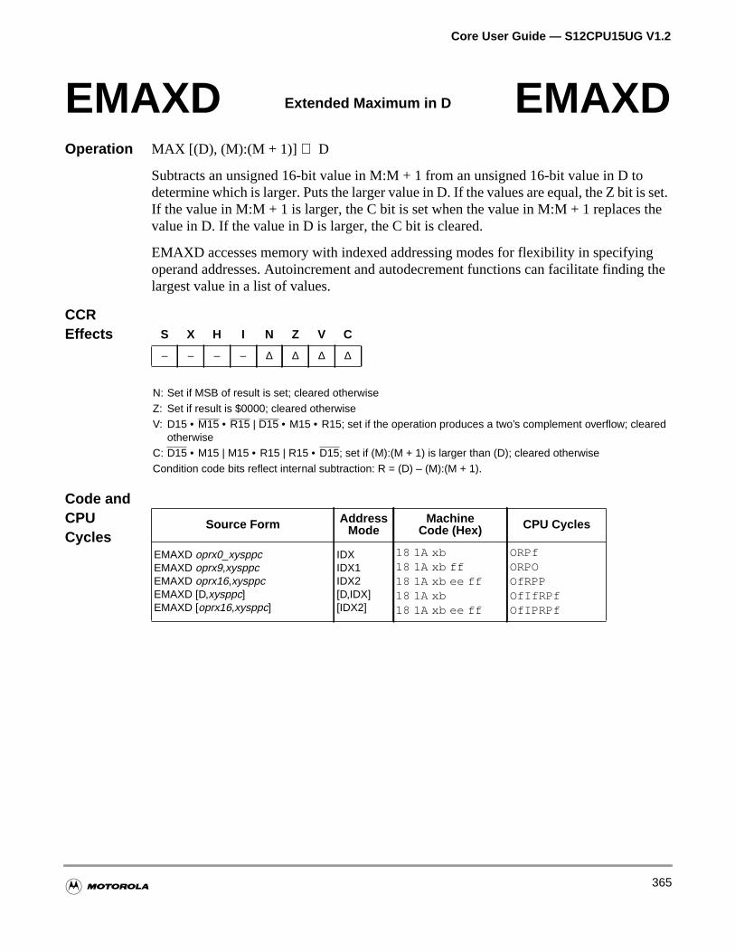
Core User Guide — S12CPU15UG V1.2
set.the
gg the
Operation MAX [(D), (M):(M + 1)] ⇒ D
Subtracts an unsigned 16-bit value in M:M + 1 from an unsigned 16-bit value in D todetermine which is larger. Puts the larger value in D. If the values are equal, the Z bit isIf the value in M:M + 1 is larger, the C bit is set when the value in M:M + 1 replaces value in D. If the value in D is larger, the C bit is cleared.
EMAXD accesses memory with indexed addressing modes for flexibility in specifyinoperand addresses. Autoincrement and autodecrement functions can facilitate findinlargest value in a list of values.
CCREffects
Code andCPUCycles
EMAXD Extended Maximum in D EMAXD
S X H I N Z V C
– – – – ∆ ∆ ∆ ∆
N: Set if MSB of result is set; cleared otherwiseZ: Set if result is $0000; cleared otherwiseV: D15 • M15 • R15 | D15 • M15 • R15; set if the operation produces a two’s complement overflow; cleared
otherwiseC: D15 • M15 | M15 • R15 | R15 • D15; set if (M):(M + 1) is larger than (D); cleared otherwiseCondition code bits reflect internal subtraction: R = (D) – (M):(M + 1).
Source Form AddressMode
MachineCode (Hex) CPU Cycles
EMAXD oprx0_xysppcEMAXD oprx9,xysppcEMAXD oprx16,xysppcEMAXD [D,xysppc]EMAXD [oprx16,xysppc]
IDXIDX1IDX2[D,IDX][IDX2]
18 1A xb18 1A xb ff18 1A xb ee ff18 1A xb18 1A xb ee ff
ORPfORPOOfRPPOfIfRPfOfIPRPf
365
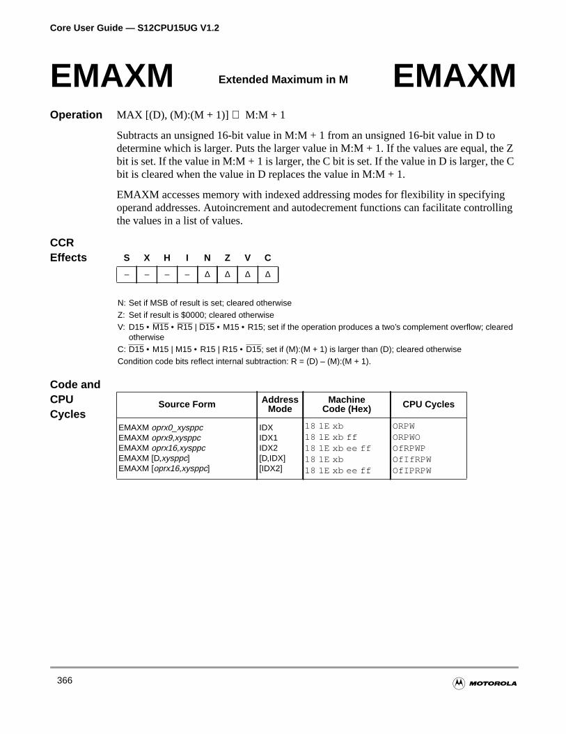
Core User Guide — S12CPU15UG V1.2
he ZC
golling
Operation MAX [(D), (M):(M + 1)] ⇒ M:M + 1
Subtracts an unsigned 16-bit value in M:M + 1 from an unsigned 16-bit value in D todetermine which is larger. Puts the larger value in M:M + 1. If the values are equal, tbit is set. If the value in M:M + 1 is larger, the C bit is set. If the value in D is larger, thebit is cleared when the value in D replaces the value in M:M + 1.
EMAXM accesses memory with indexed addressing modes for flexibility in specifyinoperand addresses. Autoincrement and autodecrement functions can facilitate contrthe values in a list of values.
CCREffects
Code andCPUCycles
EMAXM Extended Maximum in M EMAXM
S X H I N Z V C
– – – – ∆ ∆ ∆ ∆
N: Set if MSB of result is set; cleared otherwiseZ: Set if result is $0000; cleared otherwiseV: D15 • M15 • R15 | D15 • M15 • R15; set if the operation produces a two’s complement overflow; cleared
otherwiseC: D15 • M15 | M15 • R15 | R15 • D15; set if (M):(M + 1) is larger than (D); cleared otherwiseCondition code bits reflect internal subtraction: R = (D) – (M):(M + 1).
Source Form AddressMode
MachineCode (Hex) CPU Cycles
EMAXM oprx0_xysppcEMAXM oprx9,xysppcEMAXM oprx16,xysppcEMAXM [D,xysppc]EMAXM [oprx16,xysppc]
IDXIDX1IDX2[D,IDX][IDX2]
18 1E xb18 1E xb ff18 1E xb ee ff18 1E xb18 1E xb ee ff
ORPWORPWOOfRPWPOfIfRPWOfIPRPW
366

Core User Guide — S12CPU15UG V1.2
bit isis
g the
Operation MIN [(D), (M):(M + 1)] ⇒ D
Subtracts an unsigned 16-bit value in M:M + 1 from an unsigned 16-bit value in D todetermine which is larger. Puts the smaller value in D. If the values are equal, the Zset. If the value in M:M + 1 is larger, the C bit is set. If the value in D is larger, the C bitcleared when the value in M:M + 1 replaces the value in D.
EMIND accesses memory with indexed addressing modes for flexibility in specifyingoperand addresses. Autoincrement and autodecrement functions can facilitate findinsmallest value in a list of values.
CCREffects
Code andCPUCycles
EMIND Extended Minimum in D EMIND
S X H I N Z V C
– – – – ∆ ∆ ∆ ∆
N: Set if MSB of result is set; cleared otherwiseZ: Set if result is $0000; cleared otherwiseV: D15 • M15 • R15 | D15 • M15 • R15; set if the operation produces a two’s complement overflow; cleared
otherwiseC: D15 • M15 | M15 • R15 | R15 • D15; set if (M):(M + 1) is larger than (D); cleared otherwiseCondition code bits reflect internal subtraction: R = (D) – (M):(M + 1).
Source Form AddressMode
MachineCode (Hex) CPU Cycles
EMIND oprx0_xysppcEMIND oprx9,xysppcEMIND oprx16,xysppcEMIND [D,xysppc]EMIND [oprx16,xysppc]
IDXIDX1IDX2[D,IDX][IDX2]
18 1B xb18 1B xb ff18 1B xb ee ff18 1B xb18 1B xb ee ff
ORPfORPOOfRPPOfIfRPfOfIPRPf
367
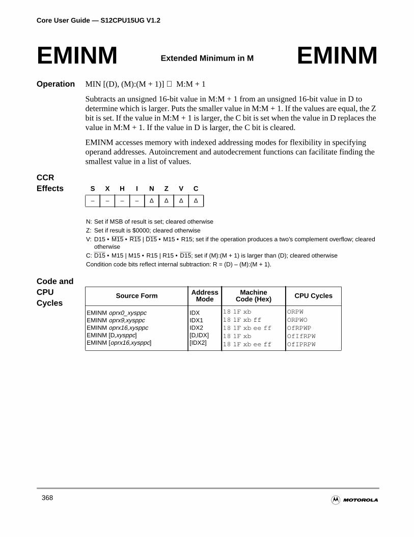
Core User Guide — S12CPU15UG V1.2
e Zthe
g the
Operation MIN [(D), (M):(M + 1)] ⇒ M:M + 1
Subtracts an unsigned 16-bit value in M:M + 1 from an unsigned 16-bit value in D todetermine which is larger. Puts the smaller value in M:M + 1. If the values are equal, thbit is set. If the value in M:M + 1 is larger, the C bit is set when the value in D replacesvalue in M:M + 1. If the value in D is larger, the C bit is cleared.
EMINM accesses memory with indexed addressing modes for flexibility in specifyingoperand addresses. Autoincrement and autodecrement functions can facilitate findinsmallest value in a list of values.
CCREffects
Code andCPUCycles
EMINM Extended Minimum in M EMINM
S X H I N Z V C
– – – – ∆ ∆ ∆ ∆
N: Set if MSB of result is set; cleared otherwiseZ: Set if result is $0000; cleared otherwiseV: D15 • M15 • R15 | D15 • M15 • R15; set if the operation produces a two’s complement overflow; cleared
otherwiseC: D15 • M15 | M15 • R15 | R15 • D15; set if (M):(M + 1) is larger than (D); cleared otherwiseCondition code bits reflect internal subtraction: R = (D) – (M):(M + 1).
Source Form AddressMode
MachineCode (Hex) CPU Cycles
EMINM oprx0_xysppcEMINM oprx9,xysppcEMINM oprx16,xysppcEMINM [D,xysppc]EMINM [oprx16,xysppc]
IDXIDX1IDX2[D,IDX][IDX2]
18 1F xb18 1F xb ff18 1F xb ee ff18 1F xb18 1F xb ee ff
ORPWORPWOOfRPWPOfIfRPWOfIPRPW
368
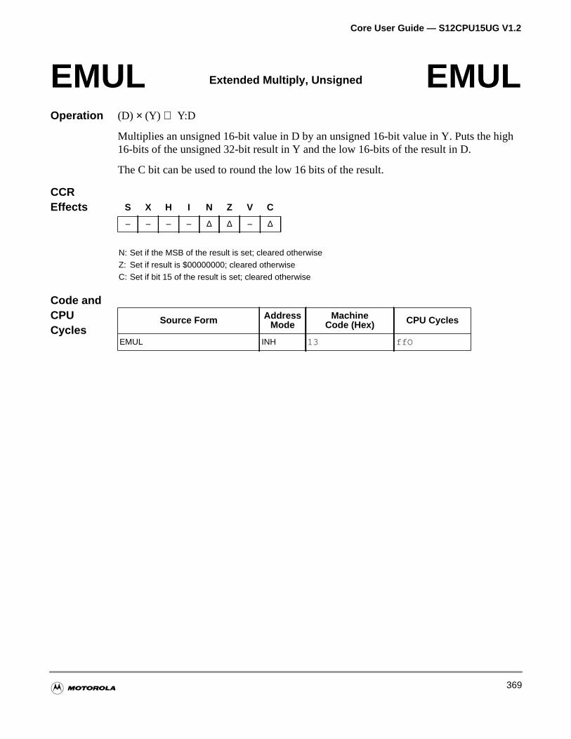
Core User Guide — S12CPU15UG V1.2
igh
Operation (D) × (Y) ⇒ Y:D
Multiplies an unsigned 16-bit value in D by an unsigned 16-bit value in Y. Puts the h16-bits of the unsigned 32-bit result in Y and the low 16-bits of the result in D.
The C bit can be used to round the low 16 bits of the result.
CCREffects
Code andCPUCycles
EMUL Extended Multiply, Unsigned EMUL
S X H I N Z V C
– – – – ∆ ∆ – ∆
N: Set if the MSB of the result is set; cleared otherwiseZ: Set if result is $00000000; cleared otherwiseC: Set if bit 15 of the result is set; cleared otherwise
Source Form AddressMode
MachineCode (Hex) CPU Cycles
EMUL INH 13 ffO
369
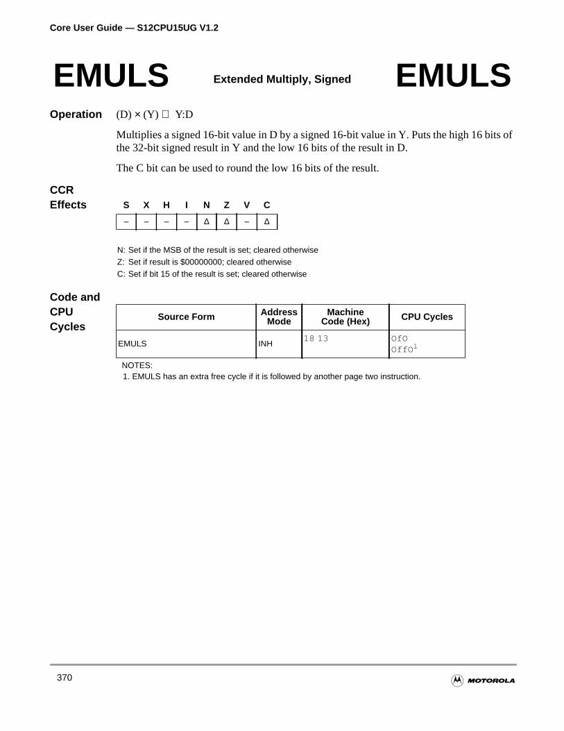
Core User Guide — S12CPU15UG V1.2
of
Operation (D) × (Y) ⇒ Y:D
Multiplies a signed 16-bit value in D by a signed 16-bit value in Y. Puts the high 16 bitsthe 32-bit signed result in Y and the low 16 bits of the result in D.
The C bit can be used to round the low 16 bits of the result.
CCREffects
Code andCPUCycles
EMULS Extended Multiply, Signed EMULS
S X H I N Z V C
– – – – ∆ ∆ – ∆
N: Set if the MSB of the result is set; cleared otherwiseZ: Set if result is $00000000; cleared otherwiseC: Set if bit 15 of the result is set; cleared otherwise
Source Form AddressMode
MachineCode (Hex) CPU Cycles
EMULS INH18 13 OfO
OffO 1
NOTES:1. EMULS has an extra free cycle if it is followed by another page two instruction.
370
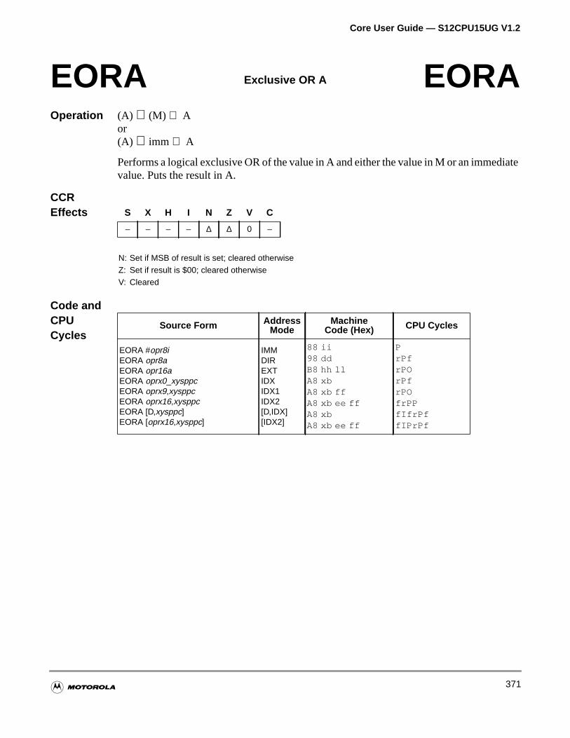
Core User Guide — S12CPU15UG V1.2
iate
Operation (A) ⊕ (M) ⇒ Aor(A) ⊕ imm ⇒ A
Performs a logical exclusive OR of the value in A and either the value in M or an immedvalue. Puts the result in A.
CCREffects
Code andCPUCycles
EORA Exclusive OR A EORA
S X H I N Z V C
– – – – ∆ ∆ 0 –
N: Set if MSB of result is set; cleared otherwiseZ: Set if result is $00; cleared otherwiseV: Cleared
Source Form AddressMode
MachineCode (Hex) CPU Cycles
EORA #opr8iEORA opr8aEORA opr16aEORA oprx0_xysppcEORA oprx9,xysppcEORA oprx16,xysppcEORA [D,xysppc]EORA [oprx16,xysppc]
IMMDIREXTIDXIDX1IDX2[D,IDX][IDX2]
88 ii98 ddB8 hh llA8 xbA8 xb ffA8 xb ee ffA8 xbA8 xb ee ff
PrPfrPOrPfrPOfrPPfIfrPffIPrPf
371
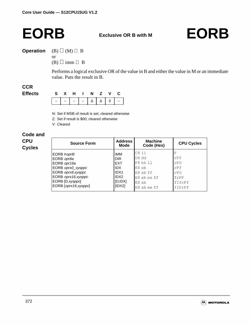
Core User Guide — S12CPU15UG V1.2
iate
Operation (B) ⊕ (M) ⇒ Bor(B) ⊕ imm ⇒ B
Performs a logical exclusive OR of the value in B and either the value in M or an immedvalue. Puts the result in B.
CCREffects
Code andCPUCycles
EORB Exclusive OR B with M EORB
S X H I N Z V C
– – – – ∆ ∆ 0 –
N: Set if MSB of result is set; cleared otherwiseZ: Set if result is $00; cleared otherwiseV: Cleared
Source Form AddressMode
MachineCode (Hex) CPU Cycles
EORB #opr8iEORB opr8aEORB opr16aEORB oprx0_xysppcEORB oprx9,xysppcEORB oprx16,xysppcEORB [D,xysppc]EORB [oprx16,xysppc]
IMMDIREXTIDXIDX1IDX2[D,IDX][IDX2]
C8 iiD8 ddF8 hh llE8 xbE8 xb ffE8 xb ee ffE8 xbE8 xb ee ff
PrPfrPOrPfrPOfrPPfIfrPffIPrPf
372
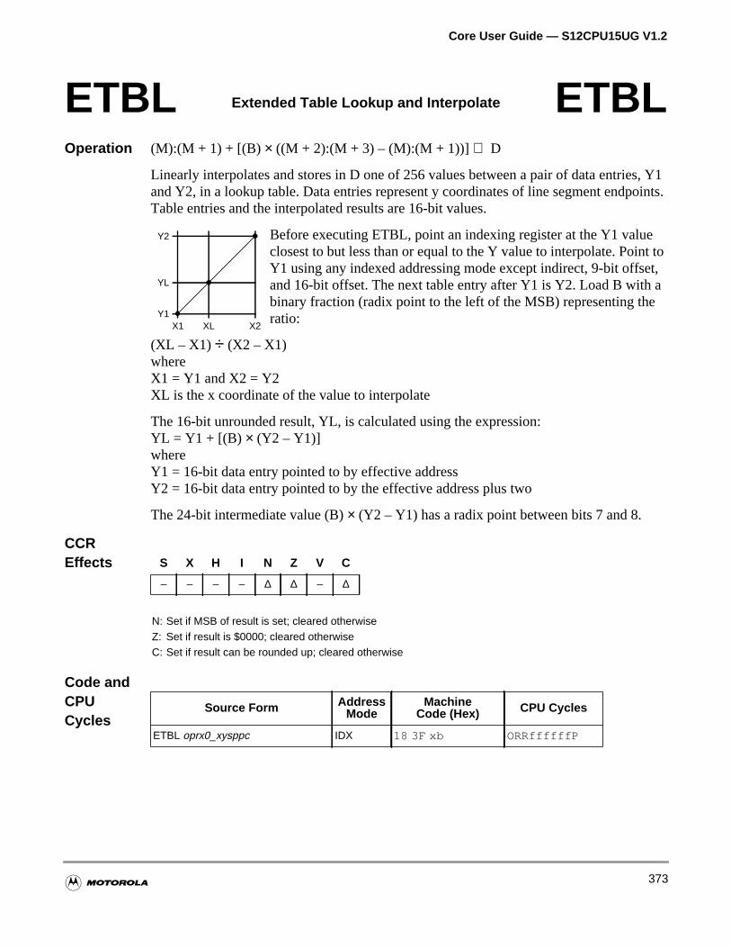
Core User Guide — S12CPU15UG V1.2
s, Y1oints.
t toet, a
Operation (M):(M + 1) + [(B) × ((M + 2):(M + 3) – (M):(M + 1))]⇒ D
Linearly interpolates and stores in D one of 256 values between a pair of data entrieand Y2, in a lookup table. Data entries represent y coordinates of line segment endpTable entries and the interpolated results are 16-bit values.
Before executing ETBL, point an indexing register at the Y1 valueclosest to but less than or equal to the Y value to interpolate. PoinY1 using any indexed addressing mode except indirect, 9-bit offsand 16-bit offset. The next table entry after Y1 is Y2. Load B withbinary fraction (radix point to the left of the MSB) representing theratio:
(XL – X1) ÷ (X2 – X1)whereX1 = Y1 and X2 = Y2XL is the x coordinate of the value to interpolate
The 16-bit unrounded result, YL, is calculated using the expression:YL = Y1 + [(B) × (Y2 – Y1)]whereY1 = 16-bit data entry pointed to by effective addressY2 = 16-bit data entry pointed to by the effective address plus two
The 24-bit intermediate value (B)× (Y2 – Y1) has a radix point between bits 7 and 8.
CCREffects
Code andCPUCycles
ETBL Extended Table Lookup and Interpolate ETBL
X1 X2Y1
Y2
XL
YL
S X H I N Z V C
– – – – ∆ ∆ – ∆
N: Set if MSB of result is set; cleared otherwiseZ: Set if result is $0000; cleared otherwiseC: Set if result can be rounded up; cleared otherwise
Source Form AddressMode
MachineCode (Hex) CPU Cycles
ETBL oprx0_xysppc IDX 18 3F xb ORRffffffP
373
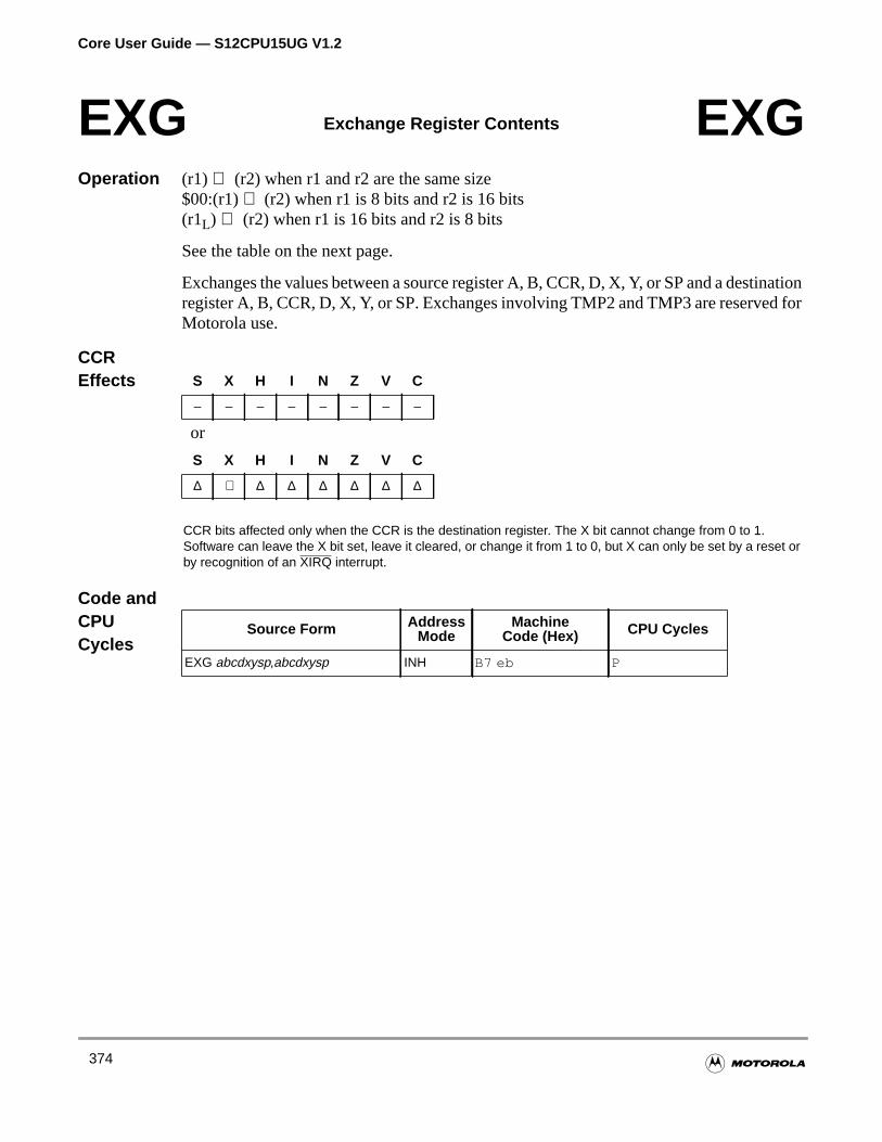
Core User Guide — S12CPU15UG V1.2
ationfor
Operation (r1) ⇔ (r2) when r1 and r2 are the same size$00:(r1)⇒ (r2) when r1 is 8 bits and r2 is 16 bits(r1L) ⇔ (r2) when r1 is 16 bits and r2 is 8 bits
See the table on the next page.
Exchanges the values between a source register A, B, CCR, D, X, Y, or SP and a destinregister A, B, CCR, D, X, Y, or SP. Exchanges involving TMP2 and TMP3 are reservedMotorola use.
CCREffects
Code andCPUCycles
EXG Exchange Register Contents EXG
S X H I N Z V C
– – – – – – – –
or
S X H I N Z V C
∆ ⇓ ∆ ∆ ∆ ∆ ∆ ∆
CCR bits affected only when the CCR is the destination register. The X bit cannot change from 0 to 1.Software can leave the X bit set, leave it cleared, or change it from 1 to 0, but X can only be set by a reset orby recognition of an XIRQ interrupt.
Source Form AddressMode
MachineCode (Hex) CPU Cycles
EXG abcdxysp,abcdxysp INH B7 eb P
374
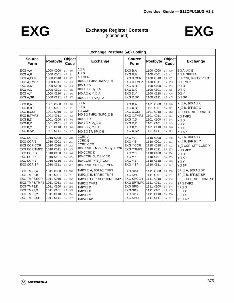
Core User Guide — S12CPU15UG V1.2
EXG Exchange Register Contents(continued) EXG
Exchange Postbyte ( eb) Coding
SourceForm
PostbyteObjectCode
ExchangeSourceForm
PostbyteObjectCode
Exchange
EXG A,AEXG A,BEXG A,CCREXG A,TMP2EXG A,DEXG A,XEXG A,YEXG A,SP
1000 X0001000 X0011000 X0101000 X0111000 X1001000 X1011000 X1101000 X111
B7 80B7 81B7 82B7 83B7 84B7 85B7 86B7 87
A⇔AA⇔BA⇔CCR$00:A⇒TMP2, TMP2L⇒A$00:A⇒D$00:A⇒X, XL⇒A$00:A⇒Y, YL⇒A$00:A⇒SP, SPL⇒A
EXG B,AEXG B,BEXG B,CCREXG D,TMP2EXG D,DEXG D,XEXG D,YEXG D,SP
1100 X0001100 X0011100 X0101100 X0111100 X1001100 X1011100 X1101100 X111
B7 C0B7 C1B7 C2B7 C3B7 C4B7 C5B7 C6B7 C7
B⇒A, A⇒BB⇒B, $FF⇒AB⇒CCR, $FF:CCR⇒DD⇔TMP2D⇔DD⇔XD⇔YD⇔SP
EXG B,AEXG B,BEXG B,CCREXG B,TMP2EXG B,DEXG B,XEXG B,YEXG B,SP
1001 X0001001 X0011001 X0101001 X0111001 X1001001 X1011001 X1101001 X111
B7 90B7 91B7 92B7 93B7 94B7 95B7 96B7 97
B⇔AB⇔BB⇔CCR$00:B⇒TMP2, TMP2L⇒B$00:B⇒D$00:B⇒X, XL⇒B$00:B⇒Y, YL⇒B$00:B⇒SP, SPL⇒B
EXG X,AEXG X,BEXG X,CCREXG X,TMP2EXG X,DEXG X,XEXG X,YEXG X,SP
1101 X0001101 X0011101 X0101101 X0111101 X1001101 X1011101 X1101101 X111
B7 D0B7 D1B7 D2B7 D3B7 D4B7 D5B7 D6B7 D7
XL⇒A, $00:A⇒XXL⇒B, $FF:B⇒XXL⇒CCR, $FF:CCR⇒XX⇔TMP2X⇔DX⇔XX⇔YX⇔SP
EXG CCR,AEXG CCR,BEXG CCR,CCREXG CCR,TMP2EXG CCR,DEXG CCR,XEXG CCR,YEXG CCR,SP
1010 X0001010 X0011010 X0101010 X0111010 X1001010 X1011010 X1101010 X111
B7 A0B7 A1B7 A2B7 A3B7 A4B7 A5B7 A6B7 A7
CCR⇔ACCR⇔BCCR⇔CCR$00:CCR⇒TMP2, TMP2L⇒CCR$00:CCR⇒D$00:CCR⇒X, XL⇒CCR$00:CCR⇒Y, YL⇒CCR$00:CCR⇒SP, SPL⇒CCR
EXG Y,AEXG Y,BEXG Y,CCREXG Y,TMP2EXG Y,DEXG Y,XEXG Y,YEXG Y,SP
1110 X0001110 X0011110 X0101110 X0111110 X1001110 X1011110 X1101110 X111
B7 E0B7 E1B7 E2B7 E3B7 E4B7 E5B7 E6B7 E7
YL⇒A, $00:A⇒YYL⇒B, $FF:B⇒YYL⇒CCR, $FF:CCR⇒YY⇔TMP2Y⇔DY⇔XY⇔YY⇔SP
EXG TMP3,AEXG TMP3,BEXG TMP3,CCREXG TMP3,TMP2EXG TMP3,DEXG TMP3,XEXG TMP3,YEXG TMP3,SP
1011 X0001011 X0011011 X0101011 X0111011 X1001011 X1011011 X1101011 X111
B7 B0B7 B1B7 B2B7 B3B7 B4B7 B5B7 B6B7 B7
TMP3L⇒A, $00:A⇒TMP3TMP3L⇒B, $FF:B⇒TMP3TMP3L⇒CCR, $FF:CCR⇒TMP3TMP3⇔TMP2TMP3⇔DTMP3⇔XTMP3⇔YTMP3⇔SP
EXG SP,AEXG SP,BEXG SP,CCREXG SP,TMP2EXG SP,DEXG SP,XEXG SP,YEXG SP,SP
1111 X0001111 X0011111 X0101111 X0111111 X1001111 X1011111 X1101111 X111
B7 F0B7 F1B7 F2B7 F3B7 F4B7 F5B7 F6B7 F7
SPL⇒A, $00:A⇒SPSPL⇒B, $FF:B⇒SPSPL⇒CCR, $FF:CCR⇒SPSP⇔TMP2SP⇔DSP⇔XSP⇔YSP⇔SP
375
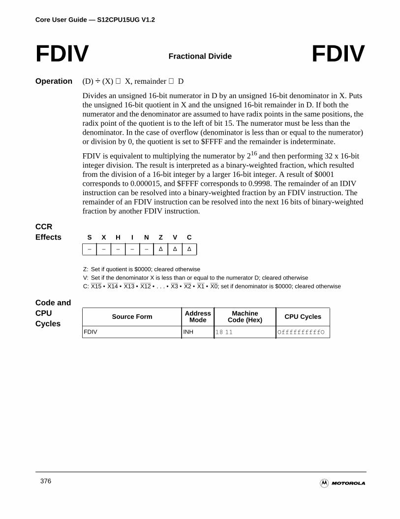
Core User Guide — S12CPU15UG V1.2
Puts
ns, theerator)
d
DIVheted
Operation (D) ÷ (X) ⇒ X, remainder⇒ D
Divides an unsigned 16-bit numerator in D by an unsigned 16-bit denominator in X. the unsigned 16-bit quotient in X and the unsigned 16-bit remainder in D. If both thenumerator and the denominator are assumed to have radix points in the same positioradix point of the quotient is to the left of bit 15. The numerator must be less than thdenominator. In the case of overflow (denominator is less than or equal to the numeor division by 0, the quotient is set to $FFFF and the remainder is indeterminate.
FDIV is equivalent to multiplying the numerator by 216and then performing 32 x 16-bitinteger division. The result is interpreted as a binary-weighted fraction, which resultefrom the division of a 16-bit integer by a larger 16-bit integer. A result of $0001corresponds to 0.000015, and $FFFF corresponds to 0.9998. The remainder of an Iinstruction can be resolved into a binary-weighted fraction by an FDIV instruction. Tremainder of an FDIV instruction can be resolved into the next 16 bits of binary-weighfraction by another FDIV instruction.
CCREffects
Code andCPUCycles
FDIV Fractional Divide FDIV
S X H I N Z V C
– – – – – ∆ ∆ ∆
Z: Set if quotient is $0000; cleared otherwiseV: Set if the denominator X is less than or equal to the numerator D; cleared otherwiseC: X15 • X14 • X13 • X12 • . . . • X3 • X2 • X1 • X0; set if denominator is $0000; cleared otherwise
Source Form AddressMode
MachineCode (Hex) CPU Cycles
FDIV INH 18 11 OffffffffffO
376
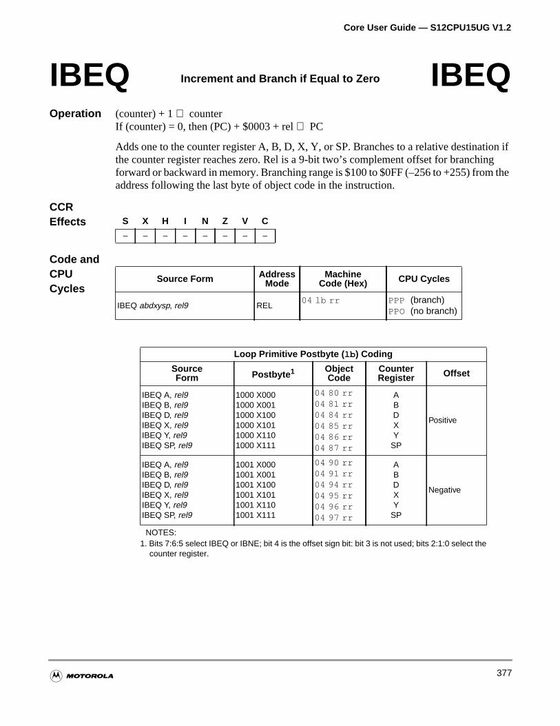
Core User Guide — S12CPU15UG V1.2
n ifngthe
Operation (counter) + 1⇒ counterIf (counter) = 0, then (PC) + $0003 + rel⇒ PC
Adds one to the counter register A, B, D, X, Y, or SP. Branches to a relative destinatiothe counter register reaches zero. Rel is a 9-bit two’s complement offset for branchiforward or backward in memory. Branching range is $100 to $0FF (–256 to +255) fromaddress following the last byte of object code in the instruction.
CCREffects
Code andCPUCycles
IBEQ Increment and Branch if Equal to Zero IBEQ
S X H I N Z V C
– – – – – – – –
Source Form AddressMode
MachineCode (Hex) CPU Cycles
IBEQ abdxysp, rel9 REL04 lb rr PPP (branch)
PPO (no branch)
Loop Primitive Postbyte ( lb ) Coding
SourceForm Postbyte 1
NOTES:1. Bits 7:6:5 select IBEQ or IBNE; bit 4 is the offset sign bit: bit 3 is not used; bits 2:1:0 select the
counter register.
ObjectCode
CounterRegister Offset
IBEQ A, rel9IBEQ B, rel9IBEQ D, rel9IBEQ X, rel9IBEQ Y, rel9IBEQ SP, rel9
1000 X0001000 X0011000 X1001000 X1011000 X1101000 X111
04 80 rr04 81 rr04 84 rr04 85 rr04 86 rr04 87 rr
ABDXY
SP
Positive
IBEQ A, rel9IBEQ B, rel9IBEQ D, rel9IBEQ X, rel9IBEQ Y, rel9IBEQ SP, rel9
1001 X0001001 X0011001 X1001001 X1011001 X1101001 X111
04 90 rr04 91 rr04 94 rr04 95 rr04 96 rr04 97 rr
ABDXY
SP
Negative
377
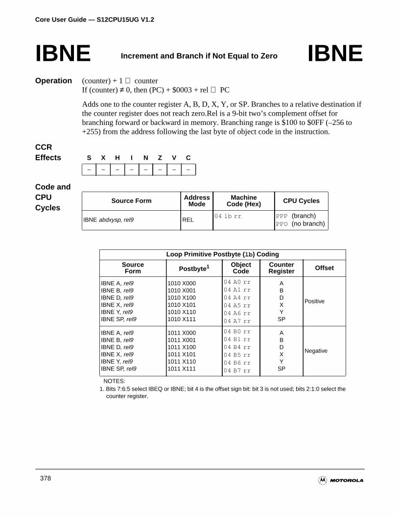
Core User Guide — S12CPU15UG V1.2
n if
to
Operation (counter) + 1⇒ counterIf (counter)≠ 0, then (PC) + $0003 + rel⇒ PC
Adds one to the counter register A, B, D, X, Y, or SP. Branches to a relative destinatiothe counter register does not reach zero.Rel is a 9-bit two’s complement offset forbranching forward or backward in memory. Branching range is $100 to $0FF (–256 +255) from the address following the last byte of object code in the instruction.
CCREffects
Code andCPUCycles
IBNE Increment and Branch if Not Equal to Zero IBNE
S X H I N Z V C
– – – – – – – –
Source Form AddressMode
MachineCode (Hex) CPU Cycles
IBNE abdxysp, rel9 REL04 lb rr PPP (branch)
PPO (no branch)
Loop Primitive Postbyte ( lb ) Coding
SourceForm Postbyte 1
NOTES:1. Bits 7:6:5 select IBEQ or IBNE; bit 4 is the offset sign bit: bit 3 is not used; bits 2:1:0 select the
counter register.
ObjectCode
CounterRegister Offset
IBNE A, rel9IBNE B, rel9IBNE D, rel9IBNE X, rel9IBNE Y, rel9IBNE SP, rel9
1010 X0001010 X0011010 X1001010 X1011010 X1101010 X111
04 A0 rr04 A1 rr04 A4 rr04 A5 rr04 A6 rr04 A7 rr
ABDXY
SP
Positive
IBNE A, rel9IBNE B, rel9IBNE D, rel9IBNE X, rel9IBNE Y, rel9IBNE SP, rel9
1011 X0001011 X0011011 X1001011 X1011011 X1101011 X111
04 B0 rr04 B1 rr04 B4 rr04 B5 rr04 B6 rr04 B7 rr
ABDXY
SP
Negative
378
Core User Guide — S12CPU15UG V1.2
isorint ofFF,
Operation (D) ÷ (X) ⇒ X; remainder⇒ D
Divides an unsigned 16-bit dividend in D by an unsigned 16-bit divisor in X. Puts theunsigned 16-bit quotient in X and the unsigned 16-bit remainder in D. If both the divand the dividend are assumed to have radix points in the same positions, the radix pothe quotient is to the right of bit 0. In the case of division by 0, the quotient is set to $FFand the remainder is indeterminate.
CCREffects
Code andCPUCycles
IDIV Integer Divide, Unsigned IDIV
S X H I N Z V C
– – – – – ∆ 0 ∆
Z: Set if quotient is $0000; cleared otherwiseV: ClearedC: X15 • X14 • X13 • X12 ... • X3 • X2 • X1 • X0; set if denominator is $0000; cleared otherwise
Source Form AddressMode
MachineCode (Hex) CPU Cycles
IDIV INH 18 10 OffffffffffO
379
Core User Guide — S12CPU15UG V1.2
-bitues
is:
mber
Operation (D) ÷ (X) ⇒ X; remainder⇒ D
Divides a signed 16-bit dividend in D by a signed 16-bit divisor in X. Puts the signed 16quotient in X and the signed 16-bit remainder in D. If division by 0 is attempted, the valin D and X do not change, but the N, Z, and V bits are undefined.
Other than division by 0, which is not legal and sets the C bit, the only overflow case
But the highest positive value that can be represented in a 16-bit two’s complement nuis 32,767 ($7FFFF).
CCREffects
Code andCPUCycles
IDIVS Integer Divide, Signed IDIVS
$8000$FFFF------------------
–32,768–1
−−−−−−−−−−−−− +32,768= =
S X H I N Z V C
– – – – ∆ ∆ ∆ ∆
N: Set if MSB of quotient is set; cleared otherwise; undefined after overflow or division by 0Z: Set if quotient is $0000; cleared otherwise; undefined after overflow or division by 0V: Set if the quotient is greater than $7FFF or less than $8000; cleared otherwise; undefined after division by
0C: X15 • X14 • X13 • X12 •... • X3 • X2 • X1 • X0; set if denominator is $0000; cleared otherwise
Source Form AddressMode
MachineCode (Hex) CPU Cycles
IDIVS INH 18 15 OffffffffffO
380
Core User Guide — S12CPU15UG V1.2
e C loop
n begned
Operation (M) + $01⇒ M
Adds one to the value in M. The N, Z, and V bits reflect the result of the operation. Thbit is not affected by the operation, thus allowing the INC instruction to be used as acounter in multiple-precision computations.
When operating on unsigned values, only BEQ, BNE, LBEQ, and LBNE branches caexpected to perform consistently. When operating on two’s complement values, all sibranches are available.
CCREffects
Code andCPUCycles
INC Increment M INC
S X H I N Z V C
– – – – ∆ ∆ ∆ –
N: Set if MSB of result is set; cleared otherwiseZ: Set if result is $00; cleared otherwiseV: Set if the operation produces a two’s complement overflow (if and only if (M) was $7F before the
operation); cleared otherwise
Source Form AddressMode
MachineCode (Hex) CPU Cycles
INC opr16aINC oprx0_xysppcINC oprx9,xysppcINC oprx16,xysppcINC [D,xysppc]INC [oprx16,xysppc]
EXTIDXIDX1IDX2[D,IDX][IDX2]
72 hh ll62 xb62 xb ff62 xb ee ff62 xb62 xb ee ff
rPwOrPwrPwOfrPwPfIfrPwfIPrPw
381
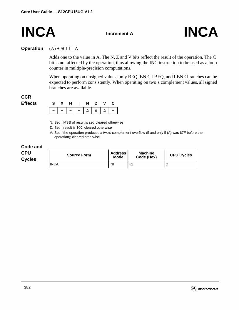
Core User Guide — S12CPU15UG V1.2
e C loop
n begned
Operation (A) + $01⇒ A
Adds one to the value in A. The N, Z and V bits reflect the result of the operation. Thbit is not affected by the operation, thus allowing the INC instruction to be used as acounter in multiple-precision computations.
When operating on unsigned values, only BEQ, BNE, LBEQ, and LBNE branches caexpected to perform consistently. When operating on two’s complement values, all sibranches are available.
CCREffects
Code andCPUCycles
INCA Increment A INCA
S X H I N Z V C
– – – – ∆ ∆ ∆ –
N: Set if MSB of result is set; cleared otherwiseZ: Set if result is $00; cleared otherwiseV: Set if the operation produces a two’s complement overflow (if and only if (A) was $7F before the
operation); cleared otherwise
Source Form AddressMode
MachineCode (Hex) CPU Cycles
INCA INH 42 O
382
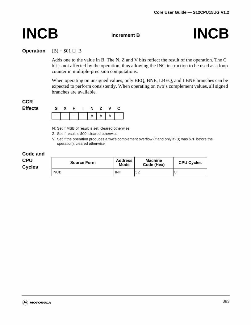
Core User Guide — S12CPU15UG V1.2
e C loop
n begned
Operation (B) + $01⇒ B
Adds one to the value in B. The N, Z and V bits reflect the result of the operation. Thbit is not affected by the operation, thus allowing the INC instruction to be used as acounter in multiple-precision computations.
When operating on unsigned values, only BEQ, BNE, LBEQ, and LBNE branches caexpected to perform consistently. When operating on two’s complement values, all sibranches are available.
CCREffects
Code andCPUCycles
INCB Increment B INCB
S X H I N Z V C
– – – – ∆ ∆ ∆ –
N: Set if MSB of result is set; cleared otherwiseZ: Set if result is $00; cleared otherwiseV: Set if the operation produces a two’s complement overflow (if and only if (B) was $7F before the
operation); cleared otherwise
Source Form AddressMode
MachineCode (Hex) CPU Cycles
INCB INH 52 O
383
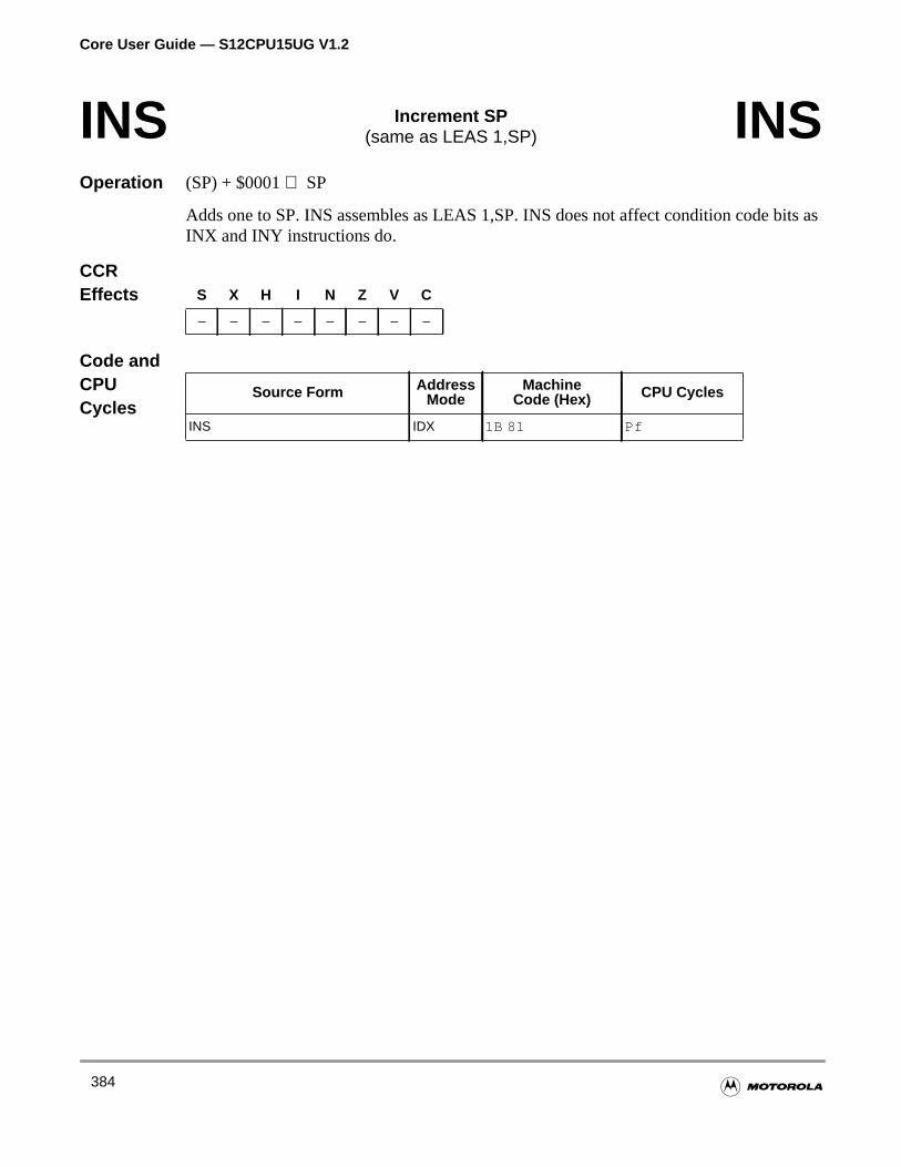
Core User Guide — S12CPU15UG V1.2
bits as
Operation (SP) + $0001⇒ SP
Adds one to SP. INS assembles as LEAS 1,SP. INS does not affect condition code INX and INY instructions do.
CCREffects
Code andCPUCycles
INS Increment SP(same as LEAS 1,SP) INS
S X H I N Z V C
– – – – – – – –
Source Form AddressMode
MachineCode (Hex) CPU Cycles
INS IDX 1B 81 Pf
384
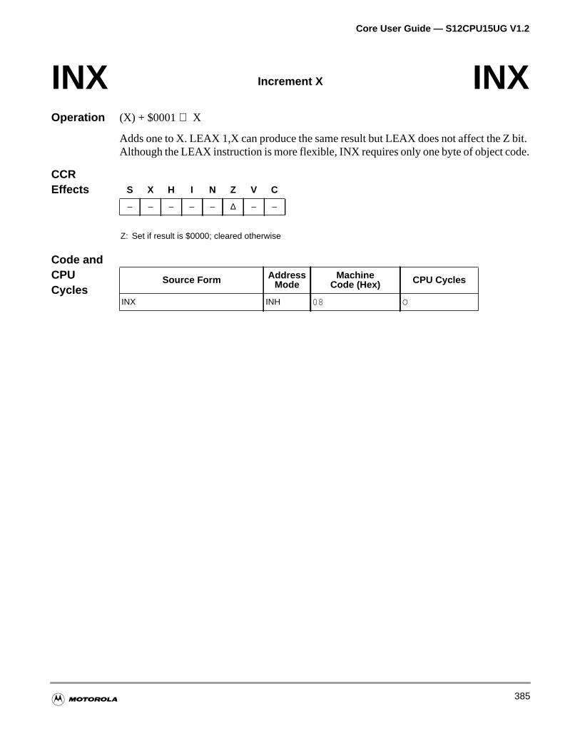
Core User Guide — S12CPU15UG V1.2
bit.e.
Operation (X) + $0001⇒ X
Adds one to X. LEAX 1,X can produce the same result but LEAX does not affect the ZAlthough the LEAX instruction is more flexible, INX requires only one byte of object cod
CCREffects
Code andCPUCycles
INX Increment X INX
S X H I N Z V C
– – – – – ∆ – –
Z: Set if result is $0000; cleared otherwise
Source Form AddressMode
MachineCode (Hex) CPU Cycles
INX INH 08 O
385
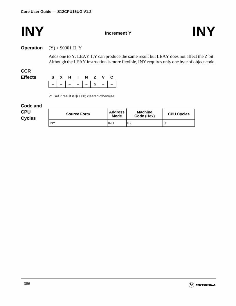
Core User Guide — S12CPU15UG V1.2
bit.e.
Operation (Y) + $0001⇒ Y
Adds one to Y. LEAY 1,Y can produce the same result but LEAY does not affect the ZAlthough the LEAY instruction is more flexible, INY requires only one byte of object cod
CCREffects
Code andCPUCycles
INY Increment Y INY
S X H I N Z V C
– – – – – ∆ – –
Z: Set if result is $0000; cleared otherwise
Source Form AddressMode
MachineCode (Hex) CPU Cycles
INY INH 02 O
386
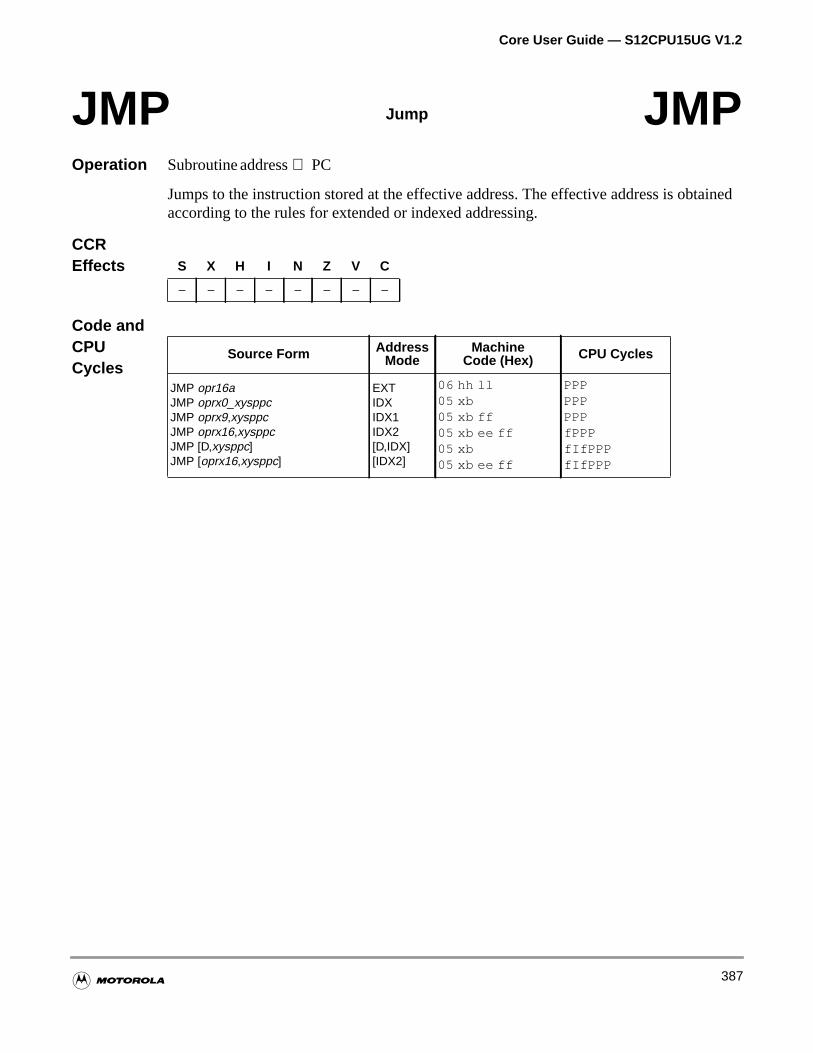
Core User Guide — S12CPU15UG V1.2
ained
Operation Subroutine address⇒ PC
Jumps to the instruction stored at the effective address. The effective address is obtaccording to the rules for extended or indexed addressing.
CCREffects
Code andCPUCycles
JMP Jump JMP
S X H I N Z V C
– – – – – – – –
Source Form AddressMode
MachineCode (Hex) CPU Cycles
JMP opr16aJMP oprx0_xysppcJMP oprx9,xysppcJMP oprx16,xysppcJMP [D,xysppc]JMP [oprx16,xysppc]
EXTIDXIDX1IDX2[D,IDX][IDX2]
06 hh ll05 xb05 xb ff05 xb ee ff05 xb05 xb ee ff
PPPPPPPPPfPPPfIfPPPfIfPPP
387
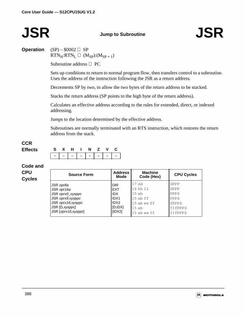
Core User Guide — S12CPU15UG V1.2
tine.
d
urn
Operation (SP) – $0002⇒ SPRTNH:RTNL ⇒ (MSP):(MSP + 1)
Subroutine address⇒ PC
Sets up conditions to return to normal program flow, then transfers control to a subrouUses the address of the instruction following the JSR as a return address.
Decrements SP by two, to allow the two bytes of the return address to be stacked.
Stacks the return address (SP points to the high byte of the return address).
Calculates an effective address according to the rules for extended, direct, or indexeaddressing.
Jumps to the location determined by the effective address.
Subroutines are normally terminated with an RTS instruction, which restores the retaddress from the stack.
CCREffects
Code andCPUCycles
JSR Jump to Subroutine JSR
S X H I N Z V C
– – – – – – – –
Source Form AddressMode
MachineCode (Hex) CPU Cycles
JSR opr8aJSR opr16aJSR oprx0_xysppcJSR oprx9,xysppcJSR oprx16,xysppcJSR [D,xysppc]JSR [oprx16,xysppc]
DIREXTIDXIDX1IDX2[D,IDX][IDX2]
17 dd16 hh ll15 xb15 xb ff15 xb ee ff15 xb15 xb ee ff
SPPPSPPPPPPSPPPSfPPPSfIfPPPSfIfPPPS
388
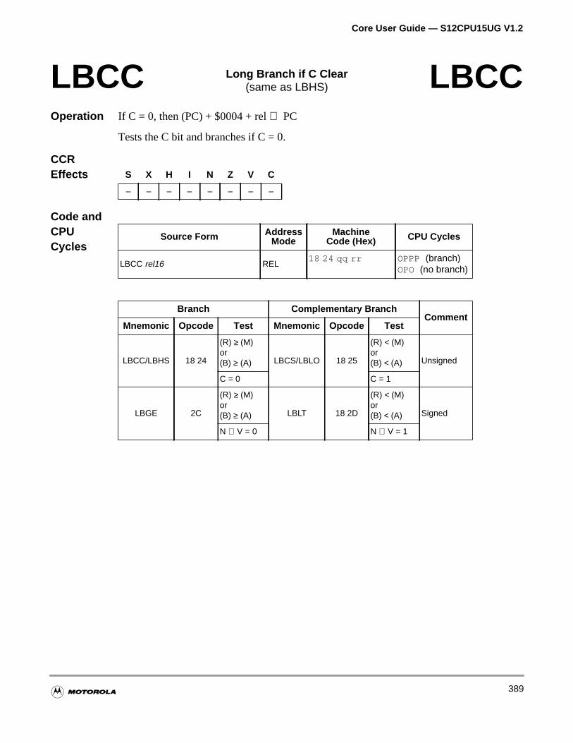
Core User Guide — S12CPU15UG V1.2
Operation If C = 0, then (PC) + $0004 + rel⇒ PC
Tests the C bit and branches if C = 0.
CCREffects
Code andCPUCycles
LBCC Long Branch if C Clear(same as LBHS) LBCC
S X H I N Z V C
– – – – – – – –
Source Form AddressMode
MachineCode (Hex) CPU Cycles
LBCC rel16 REL18 24 qq rr OPPP (branch)
OPO (no branch)
Branch Complementary BranchComment
Mnemonic Opcode Test Mnemonic Opcode Test
LBCC/LBHS 18 24
(R) ≥ (M)or(B) ≥ (A) LBCS/LBLO 18 25
(R) < (M)or(B) < (A) Unsigned
C = 0 C = 1
LBGE 2C
(R) ≥ (M)or(B) ≥ (A) LBLT 18 2D
(R) < (M)or(B) < (A) Signed
N ⊕ V = 0 N ⊕ V = 1
389
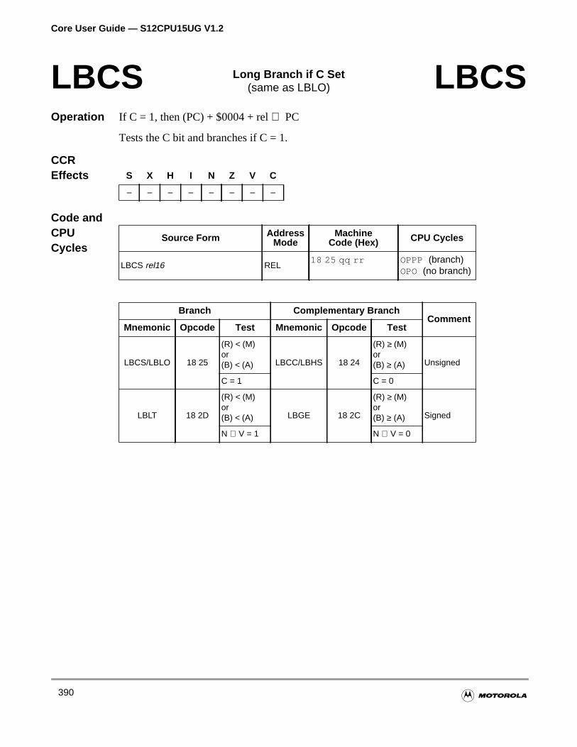
Core User Guide — S12CPU15UG V1.2
Operation If C = 1, then (PC) + $0004 + rel⇒ PC
Tests the C bit and branches if C = 1.
CCREffects
Code andCPUCycles
LBCS Long Branch if C Set(same as LBLO) LBCS
S X H I N Z V C
– – – – – – – –
Source Form AddressMode
MachineCode (Hex) CPU Cycles
LBCS rel16 REL18 25 qq rr OPPP (branch)
OPO (no branch)
Branch Complementary BranchComment
Mnemonic Opcode Test Mnemonic Opcode Test
LBCS/LBLO 18 25
(R) < (M)or(B) < (A) LBCC/LBHS 18 24
(R) ≥ (M)or(B) ≥ (A) Unsigned
C = 1 C = 0
LBLT 18 2D
(R) < (M)or(B) < (A) LBGE 18 2C
(R) ≥ (M)or(B) ≥ (A) Signed
N ⊕ V = 1 N ⊕ V = 0
390
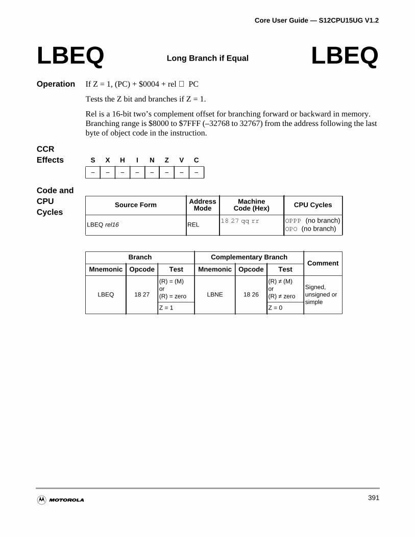
Core User Guide — S12CPU15UG V1.2
y.last
Operation If Z = 1, (PC) + $0004 + rel⇒ PC
Tests the Z bit and branches if Z = 1.
Rel is a 16-bit two’s complement offset for branching forward or backward in memorBranching range is $8000 to $7FFF (–32768 to 32767) from the address following thebyte of object code in the instruction.
CCREffects
Code andCPUCycles
LBEQ Long Branch if Equal LBEQ
S X H I N Z V C
– – – – – – – –
Source Form AddressMode
MachineCode (Hex) CPU Cycles
LBEQ rel16 REL18 27 qq rr OPPP (no branch)
OPO (no branch)
Branch Complementary BranchComment
Mnemonic Opcode Test Mnemonic Opcode Test
LBEQ 18 27
(R) = (M)or(R) = zero LBNE 18 26
(R) ≠ (M)or(R) ≠ zero
Signed,unsigned orsimple
Z = 1 Z = 0
391
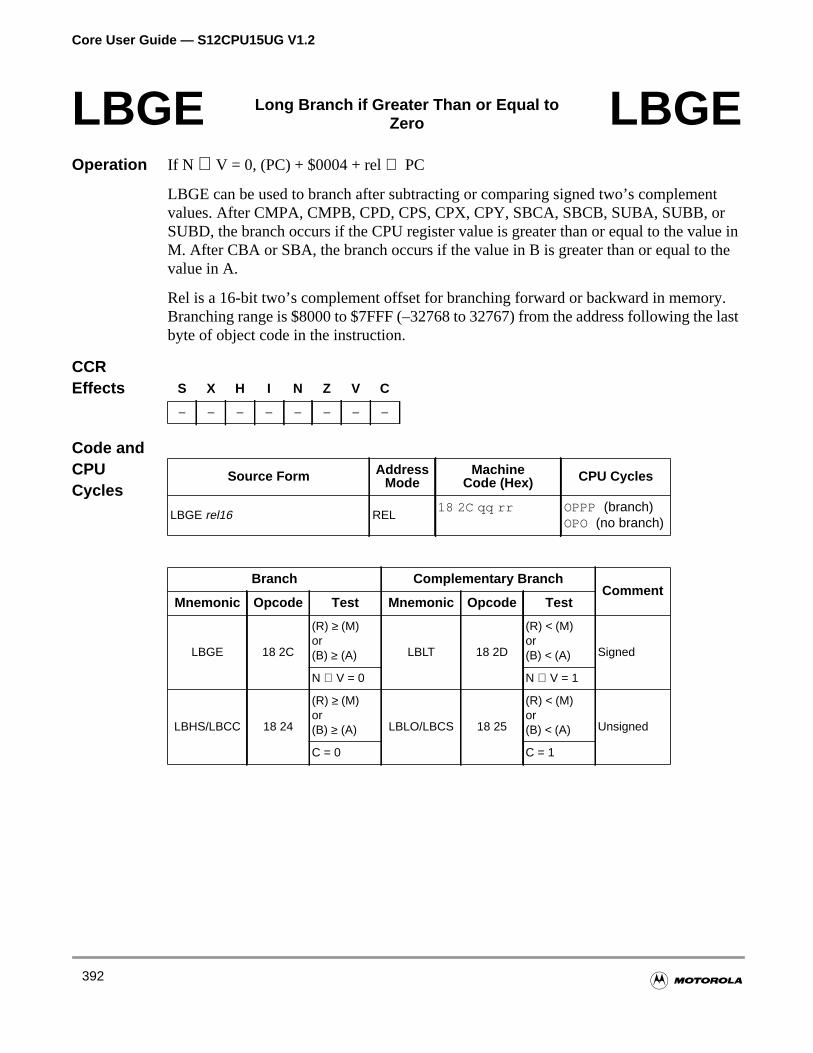
Core User Guide — S12CPU15UG V1.2
ntrue inthe
y.last
Operation If N ⊕ V = 0, (PC) + $0004 + rel⇒ PC
LBGE can be used to branch after subtracting or comparing signed two’s complemevalues. After CMPA, CMPB, CPD, CPS, CPX, CPY, SBCA, SBCB, SUBA, SUBB, oSUBD, the branch occurs if the CPU register value is greater than or equal to the valM. After CBA or SBA, the branch occurs if the value in B is greater than or equal to value in A.
Rel is a 16-bit two’s complement offset for branching forward or backward in memorBranching range is $8000 to $7FFF (–32768 to 32767) from the address following thebyte of object code in the instruction.
CCREffects
Code andCPUCycles
LBGE Long Branch if Greater Than or Equal toZero LBGE
S X H I N Z V C
– – – – – – – –
Source Form AddressMode
MachineCode (Hex) CPU Cycles
LBGE rel16 REL18 2C qq rr OPPP (branch)
OPO (no branch)
Branch Complementary BranchComment
Mnemonic Opcode Test Mnemonic Opcode Test
LBGE 18 2C
(R) ≥ (M)or(B) ≥ (A) LBLT 18 2D
(R) < (M)or(B) < (A) Signed
N ⊕ V = 0 N ⊕ V = 1
LBHS/LBCC 18 24
(R) ≥ (M)or(B) ≥ (A) LBLO/LBCS 18 25
(R) < (M)or(B) < (A) Unsigned
C = 0 C = 1
392
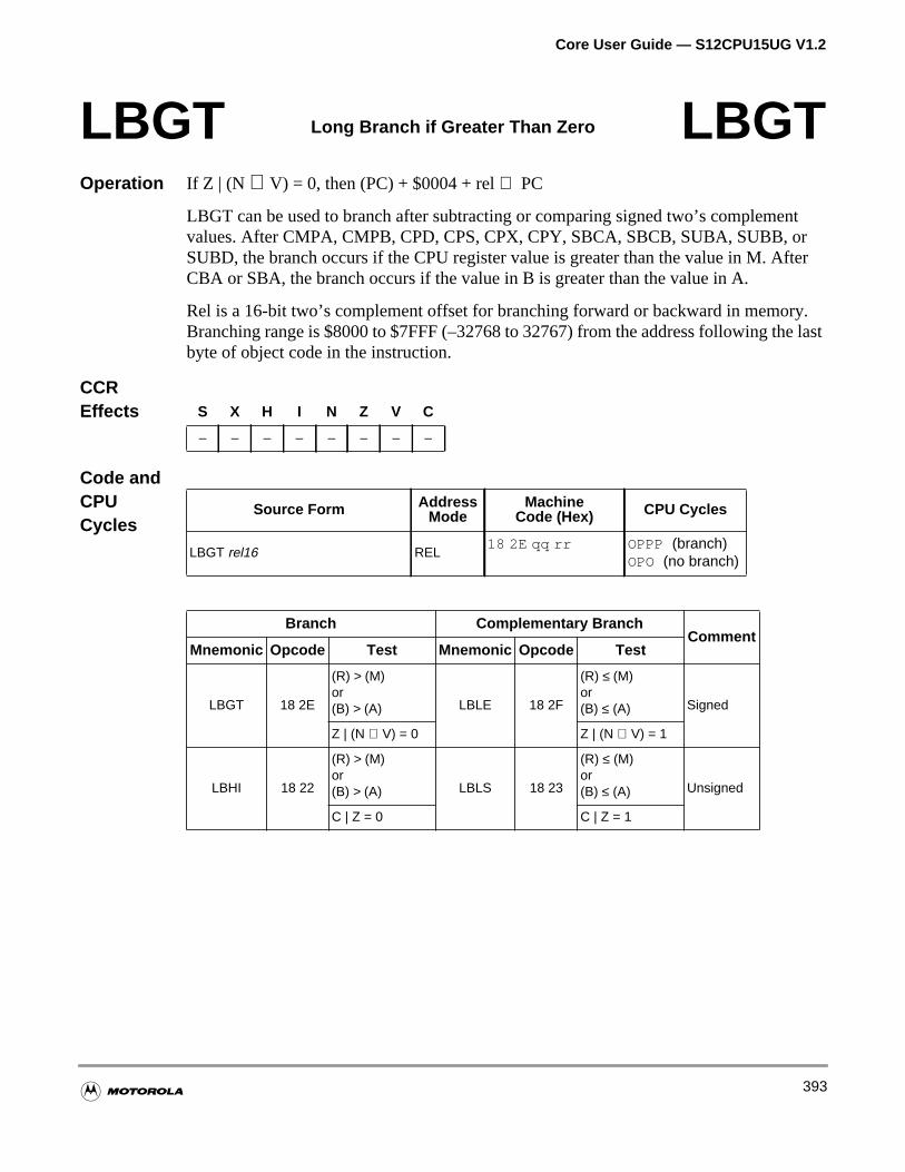
Core User Guide — S12CPU15UG V1.2
ntrfter
y.last
Operation If Z | (N ⊕ V) = 0, then (PC) + $0004 + rel⇒ PC
LBGT can be used to branch after subtracting or comparing signed two’s complemevalues. After CMPA, CMPB, CPD, CPS, CPX, CPY, SBCA, SBCB, SUBA, SUBB, oSUBD, the branch occurs if the CPU register value is greater than the value in M. ACBA or SBA, the branch occurs if the value in B is greater than the value in A.
Rel is a 16-bit two’s complement offset for branching forward or backward in memorBranching range is $8000 to $7FFF (–32768 to 32767) from the address following thebyte of object code in the instruction.
CCREffects
Code andCPUCycles
LBGT Long Branch if Greater Than Zero LBGT
S X H I N Z V C
– – – – – – – –
Source Form AddressMode
MachineCode (Hex) CPU Cycles
LBGT rel16 REL18 2E qq rr OPPP (branch)
OPO (no branch)
Branch Complementary BranchComment
Mnemonic Opcode Test Mnemonic Opcode Test
LBGT 18 2E
(R) > (M)or(B) > (A) LBLE 18 2F
(R) ≤ (M)or(B) ≤ (A) Signed
Z | (N ⊕ V) = 0 Z | (N ⊕ V) = 1
LBHI 18 22
(R) > (M)or(B) > (A) LBLS 18 23
(R) ≤ (M)or(B) ≤ (A) Unsigned
C | Z = 0 C | Z = 1
393
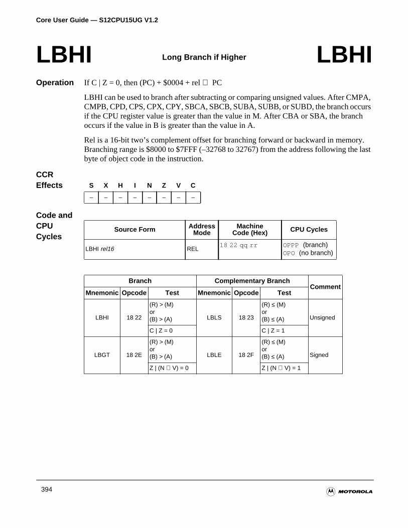
Core User Guide — S12CPU15UG V1.2
PA,ursh
y.last
Operation If C | Z = 0, then (PC) + $0004 + rel⇒ PC
LBHI can be used to branch after subtracting or comparing unsigned values. After CMCMPB, CPD, CPS, CPX, CPY, SBCA, SBCB, SUBA, SUBB, or SUBD, the branch occif the CPU register value is greater than the value in M. After CBA or SBA, the brancoccurs if the value in B is greater than the value in A.
Rel is a 16-bit two’s complement offset for branching forward or backward in memorBranching range is $8000 to $7FFF (–32768 to 32767) from the address following thebyte of object code in the instruction.
CCREffects
Code andCPUCycles
LBHI Long Branch if Higher LBHI
S X H I N Z V C
– – – – – – – –
Source Form AddressMode
MachineCode (Hex) CPU Cycles
LBHI rel16 REL18 22 qq rr OPPP (branch)
OPO (no branch)
Branch Complementary BranchComment
Mnemonic Opcode Test Mnemonic Opcode Test
LBHI 18 22
(R) > (M)or(B) > (A) LBLS 18 23
(R) ≤ (M)or(B) ≤ (A) Unsigned
C | Z = 0 C | Z = 1
LBGT 18 2E
(R) > (M)or(B) > (A) LBLE 18 2F
(R) ≤ (M)or(B) ≤ (A) Signed
Z | (N ⊕ V) = 0 Z | (N ⊕ V) = 1
394
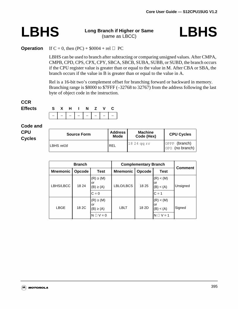
Core User Guide — S12CPU15UG V1.2
PA,ursthe
y.last
Operation If C = 0, then (PC) + $0004 + rel⇒ PC
LBHS can be used to branch after subtracting or comparing unsigned values. After CMCMPB, CPD, CPS, CPX, CPY, SBCA, SBCB, SUBA, SUBB, or SUBD, the branch occif the CPU register value is greater than or equal to the value in M. After CBA or SBA,branch occurs if the value in B is greater than or equal to the value in A.
Rel is a 16-bit two’s complement offset for branching forward or backward in memorBranching range is $8000 to $7FFF (–32768 to 32767) from the address following thebyte of object code in the instruction.
CCREffects
Code andCPUCycles
LBHS Long Branch if Higher or Same(same as LBCC) LBHS
S X H I N Z V C
– – – – – – – –
Source Form AddressMode
MachineCode (Hex) CPU Cycles
LBHS rel16 REL18 24 qq rr OPPP (branch)
OPO (no branch)
Branch Complementary BranchComment
Mnemonic Opcode Test Mnemonic Opcode Test
LBHS/LBCC 18 24
(R) ≥ (M)or(B) ≥ (A) LBLO/LBCS 18 25
(R) < (M)or(B) < (A) Unsigned
C = 0 C = 1
LBGE 18 2C
(R) ≥ (M)or(B) ≥ (A) LBLT 18 2D
(R) < (M)or(B) < (A) Signed
N ⊕ V = 0 N ⊕ V = 1
395
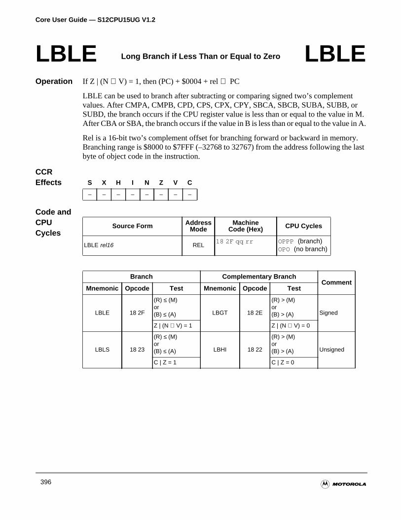
Core User Guide — S12CPU15UG V1.2
ntrn M.n A.
y.last
Operation If Z | (N ⊕ V) = 1, then (PC) + $0004 + rel⇒ PC
LBLE can be used to branch after subtracting or comparing signed two’s complemevalues. After CMPA, CMPB, CPD, CPS, CPX, CPY, SBCA, SBCB, SUBA, SUBB, oSUBD, the branch occurs if the CPU register value is less than or equal to the value iAfter CBA or SBA, the branch occurs if the value in B is less than or equal to the value i
Rel is a 16-bit two’s complement offset for branching forward or backward in memorBranching range is $8000 to $7FFF (–32768 to 32767) from the address following thebyte of object code in the instruction.
CCREffects
Code andCPUCycles
LBLE Long Branch if Less Than or Equal to Zero LBLE
S X H I N Z V C
– – – – – – – –
Source Form AddressMode
MachineCode (Hex) CPU Cycles
LBLE rel16 REL18 2F qq rr OPPP (branch)
OPO (no branch)
Branch Complementary BranchComment
Mnemonic Opcode Test Mnemonic Opcode Test
LBLE 18 2F
(R) ≤ (M)or(B) ≤ (A) LBGT 18 2E
(R) > (M)or(B) > (A) Signed
Z | (N ⊕ V) = 1 Z | (N ⊕ V) = 0
LBLS 18 23
(R) ≤ (M)or(B) ≤ (A) LBHI 18 22
(R) > (M)or(B) > (A) Unsigned
C | Z = 1 C | Z = 0
396
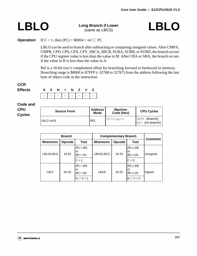
Core User Guide — S12CPU15UG V1.2
PA,ursurs
y.last
Operation If C = 1, then (PC) + $0004 + rel⇒ PC
LBLO can be used to branch after subtracting or comparing unsigned values. After CMCMPB, CPD, CPS, CPX, CPY, SBCA, SBCB, SUBA, SUBB, or SUBD, the branch occif the CPU register value is less than the value in M. After CBA or SBA, the branch occif the value in B is less than the value in A.
Rel is a 16-bit two’s complement offset for branching forward or backward in memorBranching range is $8000 to $7FFF (–32768 to 32767) from the address following thebyte of object code in the instruction.
CCREffects
Code andCPUCycles
LBLO Long Branch if Lower(same as LBCS) LBLO
S X H I N Z V C
– – – – – – – –
Source Form AddressMode
MachineCode (Hex) CPU Cycles
LBLO rel16 REL18 25 qq rr OPPP (branch)
OPO (no branch)
Branch Complementary BranchComment
Mnemonic Opcode Test Mnemonic Opcode Test
LBLO/LBCS 18 25
(R) < (M)or(B) < (A) LBHS/LBCC 18 24
(R) ≥ (M)or(B) ≥ (A) Unsigned
C = 1 C = 0
LBLT 18 2D
(R) < (M)or(B) < (A) LBGE 18 2C
(R) ≥ (M)or(B) ≥ (A) Signed
N ⊕ V = 1 N ⊕ V = 0
397
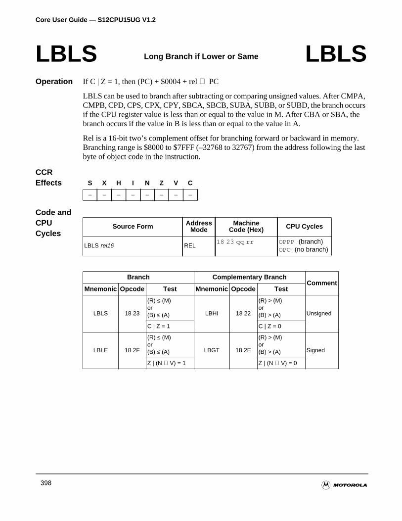
Core User Guide — S12CPU15UG V1.2
PA,urshe
y.last
Operation If C | Z = 1, then (PC) + $0004 + rel⇒ PC
LBLS can be used to branch after subtracting or comparing unsigned values. After CMCMPB, CPD, CPS, CPX, CPY, SBCA, SBCB, SUBA, SUBB, or SUBD, the branch occif the CPU register value is less than or equal to the value in M. After CBA or SBA, tbranch occurs if the value in B is less than or equal to the value in A.
Rel is a 16-bit two’s complement offset for branching forward or backward in memorBranching range is $8000 to $7FFF (–32768 to 32767) from the address following thebyte of object code in the instruction.
CCREffects
Code andCPUCycles
LBLS Long Branch if Lower or Same LBLS
S X H I N Z V C
– – – – – – – –
Source Form AddressMode
MachineCode (Hex) CPU Cycles
LBLS rel16 REL18 23 qq rr OPPP (branch)
OPO (no branch)
Branch Complementary BranchComment
Mnemonic Opcode Test Mnemonic Opcode Test
LBLS 18 23
(R) ≤ (M)or(B) ≤ (A) LBHI 18 22
(R) > (M)or(B) > (A) Unsigned
C | Z = 1 C | Z = 0
LBLE 18 2F
(R) ≤ (M)or(B) ≤ (A) LBGT 18 2E
(R) > (M)or(B) > (A) Signed
Z | (N ⊕ V) = 1 Z | (N ⊕ V) = 0
398
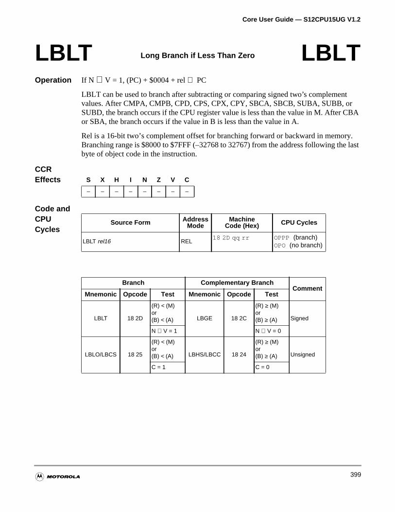
Core User Guide — S12CPU15UG V1.2
trBA
y.last
Operation If N ⊕ V = 1, (PC) + $0004 + rel⇒ PC
LBLT can be used to branch after subtracting or comparing signed two’s complemenvalues. After CMPA, CMPB, CPD, CPS, CPX, CPY, SBCA, SBCB, SUBA, SUBB, oSUBD, the branch occurs if the CPU register value is less than the value in M. After Cor SBA, the branch occurs if the value in B is less than the value in A.
Rel is a 16-bit two’s complement offset for branching forward or backward in memorBranching range is $8000 to $7FFF (–32768 to 32767) from the address following thebyte of object code in the instruction.
CCREffects
Code andCPUCycles
LBLT Long Branch if Less Than Zero LBLT
S X H I N Z V C
– – – – – – – –
Source Form AddressMode
MachineCode (Hex) CPU Cycles
LBLT rel16 REL18 2D qq rr OPPP (branch)
OPO (no branch)
Branch Complementary BranchComment
Mnemonic Opcode Test Mnemonic Opcode Test
LBLT 18 2D
(R) < (M)or(B) < (A) LBGE 18 2C
(R) ≥ (M)or(B) ≥ (A) Signed
N ⊕ V = 1 N ⊕ V = 0
LBLO/LBCS 18 25
(R) < (M)or(B) < (A) LBHS/LBCC 18 24
(R) ≥ (M)or(B) ≥ (A) Unsigned
C = 1 C = 0
399

Core User Guide — S12CPU15UG V1.2
y.last
Operation If N = 1, then (PC) + $0004 + rel⇒ PC
Tests the N bit and branches if N = 1.
Rel is a 16-bit two’s complement offset for branching forward or backward in memorBranching range is $8000 to $7FFF (–32768 to 32767) from the address following thebyte of object code in the instruction.
CCREffects
Code andCPUCycles
LBMI Long Branch if Minus LBMI
S X H I N Z V C
– – – – – – – –
Source Form AddressMode
MachineCode (Hex) CPU Cycles
LBMI rel16 REL18 2B qq rr OPPP (branch)
OPO (no branch)
Branch Complementary BranchComment
Mnemonic Opcode Test Mnemonic Opcode Test
LBMI 18 2BNegative
LBPL 18 2APositive
SimpleN = 1 N = 0
400
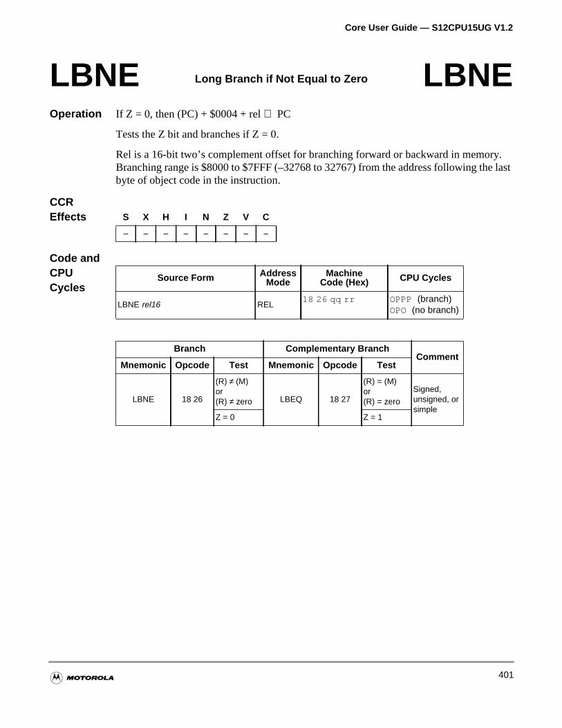
Core User Guide — S12CPU15UG V1.2
y.last
Operation If Z = 0, then (PC) + $0004 + rel⇒ PC
Tests the Z bit and branches if Z = 0.
Rel is a 16-bit two’s complement offset for branching forward or backward in memorBranching range is $8000 to $7FFF (–32768 to 32767) from the address following thebyte of object code in the instruction.
CCREffects
Code andCPUCycles
LBNE Long Branch if Not Equal to Zero LBNE
S X H I N Z V C
– – – – – – – –
Source Form AddressMode
MachineCode (Hex) CPU Cycles
LBNE rel16 REL18 26 qq rr OPPP (branch)
OPO (no branch)
Branch Complementary BranchComment
Mnemonic Opcode Test Mnemonic Opcode Test
LBNE 18 26
(R) ≠ (M)or(R) ≠ zero LBEQ 18 27
(R) = (M)or(R) = zero
Signed,unsigned, orsimple
Z = 0 Z = 1
401
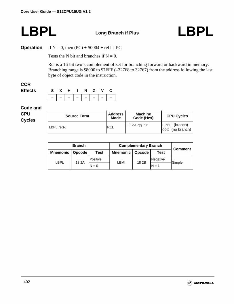
Core User Guide — S12CPU15UG V1.2
y.last
Operation If N = 0, then (PC) + $0004 + rel⇒ PC
Tests the N bit and branches if N = 0.
Rel is a 16-bit two’s complement offset for branching forward or backward in memorBranching range is $8000 to $7FFF (–32768 to 32767) from the address following thebyte of object code in the instruction.
CCREffects
Code andCPUCycles
LBPL Long Branch if Plus LBPL
S X H I N Z V C
– – – – – – – –
Source Form AddressMode
MachineCode (Hex) CPU Cycles
LBPL rel16 REL18 2A qq rr OPPP (branch)
OPO (no branch)
Branch Complementary BranchComment
Mnemonic Opcode Test Mnemonic Opcode Test
LBPL 18 2APositive
LBMI 18 2BNegative
SimpleN = 0 N = 1
402
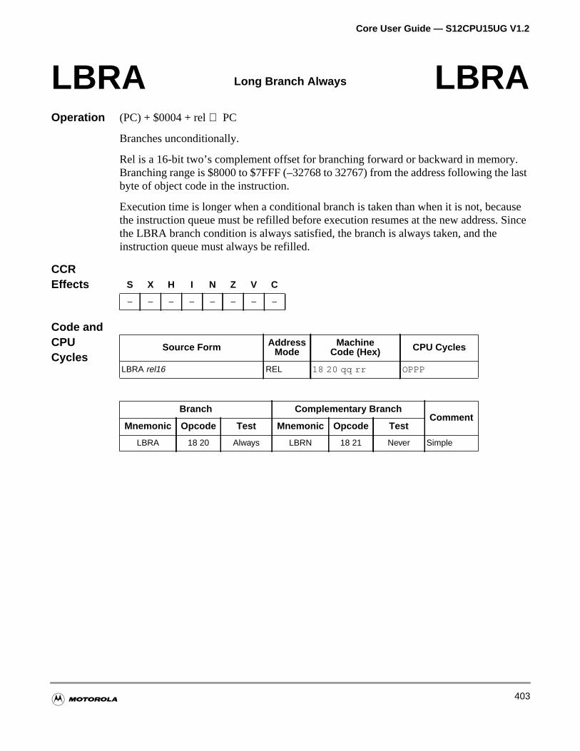
Core User Guide — S12CPU15UG V1.2
y.last
use. Since
Operation (PC) + $0004 + rel⇒ PC
Branches unconditionally.
Rel is a 16-bit two’s complement offset for branching forward or backward in memorBranching range is $8000 to $7FFF (–32768 to 32767) from the address following thebyte of object code in the instruction.
Execution time is longer when a conditional branch is taken than when it is not, becathe instruction queue must be refilled before execution resumes at the new addressthe LBRA branch condition is always satisfied, the branch is always taken, and theinstruction queue must always be refilled.
CCREffects
Code andCPUCycles
LBRA Long Branch Always LBRA
S X H I N Z V C
– – – – – – – –
Source Form AddressMode
MachineCode (Hex) CPU Cycles
LBRA rel16 REL 18 20 qq rr OPPP
Branch Complementary BranchComment
Mnemonic Opcode Test Mnemonic Opcode Test
LBRA 18 20 Always LBRN 18 21 Never Simple
403
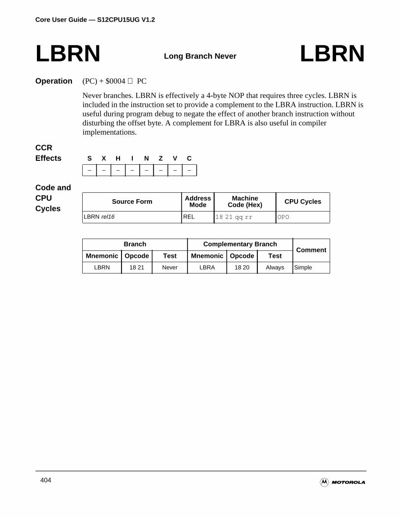
Core User Guide — S12CPU15UG V1.2
isisut
Operation (PC) + $0004⇒ PC
Never branches. LBRN is effectively a 4-byte NOP that requires three cycles. LBRNincluded in the instruction set to provide a complement to the LBRA instruction. LBRNuseful during program debug to negate the effect of another branch instruction withodisturbing the offset byte. A complement for LBRA is also useful in compilerimplementations.
CCREffects
Code andCPUCycles
LBRN Long Branch Never LBRN
S X H I N Z V C
– – – – – – – –
Source Form AddressMode
MachineCode (Hex) CPU Cycles
LBRN rel16 REL 18 21 qq rr OPO
Branch Complementary BranchComment
Mnemonic Opcode Test Mnemonic Opcode Test
LBRN 18 21 Never LBRA 18 20 Always Simple
404
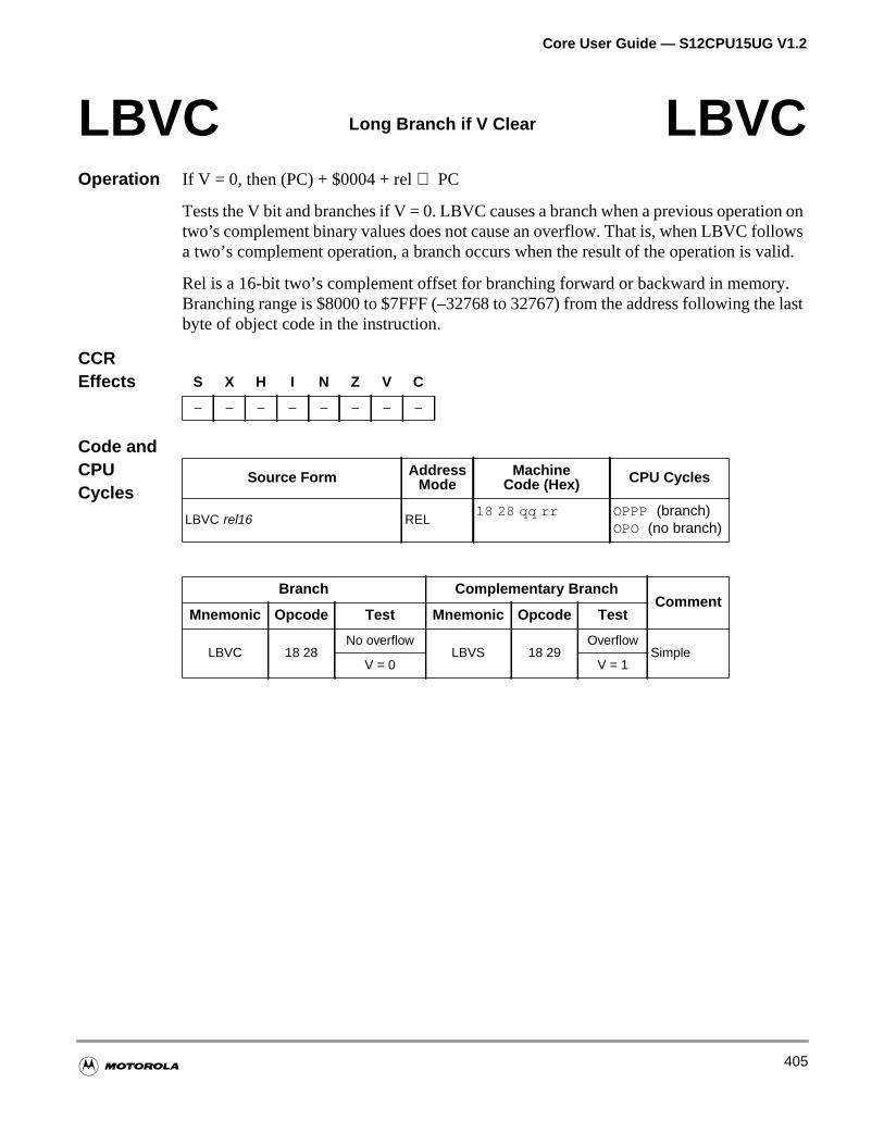
Core User Guide — S12CPU15UG V1.2
onws
alid.
y.last
Operation If V = 0, then (PC) + $0004 + rel⇒ PC
Tests the V bit and branches if V = 0. LBVC causes a branch when a previous operationtwo’s complement binary values does not cause an overflow. That is, when LBVC folloa two’s complement operation, a branch occurs when the result of the operation is v
Rel is a 16-bit two’s complement offset for branching forward or backward in memorBranching range is $8000 to $7FFF (–32768 to 32767) from the address following thebyte of object code in the instruction.
CCREffects
Code andCPUCycles
LBVC Long Branch if V Clear LBVC
S X H I N Z V C
– – – – – – – –
Source Form AddressMode
MachineCode (Hex) CPU Cycles
LBVC rel16 REL18 28 qq rr OPPP (branch)
OPO (no branch)
Branch Complementary BranchComment
Mnemonic Opcode Test Mnemonic Opcode Test
LBVC 18 28No overflow
LBVS 18 29Overflow
SimpleV = 0 V = 1
405
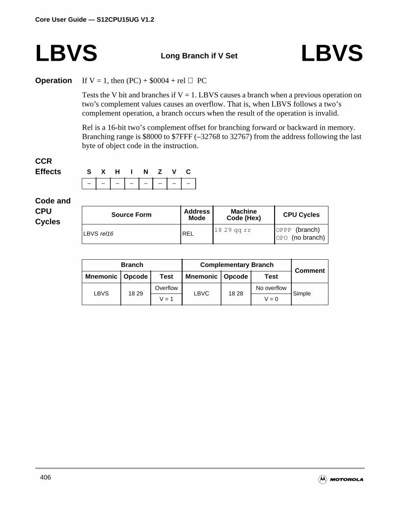
Core User Guide — S12CPU15UG V1.2
n on
y.last
Operation If V = 1, then (PC) + $0004 + rel⇒ PC
Tests the V bit and branches if V = 1. LBVS causes a branch when a previous operatiotwo’s complement values causes an overflow. That is, when LBVS follows a two’scomplement operation, a branch occurs when the result of the operation is invalid.
Rel is a 16-bit two’s complement offset for branching forward or backward in memorBranching range is $8000 to $7FFF (–32768 to 32767) from the address following thebyte of object code in the instruction.
CCREffects
Code andCPUCycles
LBVS Long Branch if V Set LBVS
S X H I N Z V C
– – – – – – – –
Source Form AddressMode
MachineCode (Hex) CPU Cycles
LBVS rel16 REL18 29 qq rr OPPP (branch)
OPO (no branch)
Branch Complementary BranchComment
Mnemonic Opcode Test Mnemonic Opcode Test
LBVS 18 29Overflow
LBVC 18 28No overflow
SimpleV = 1 V = 0
406
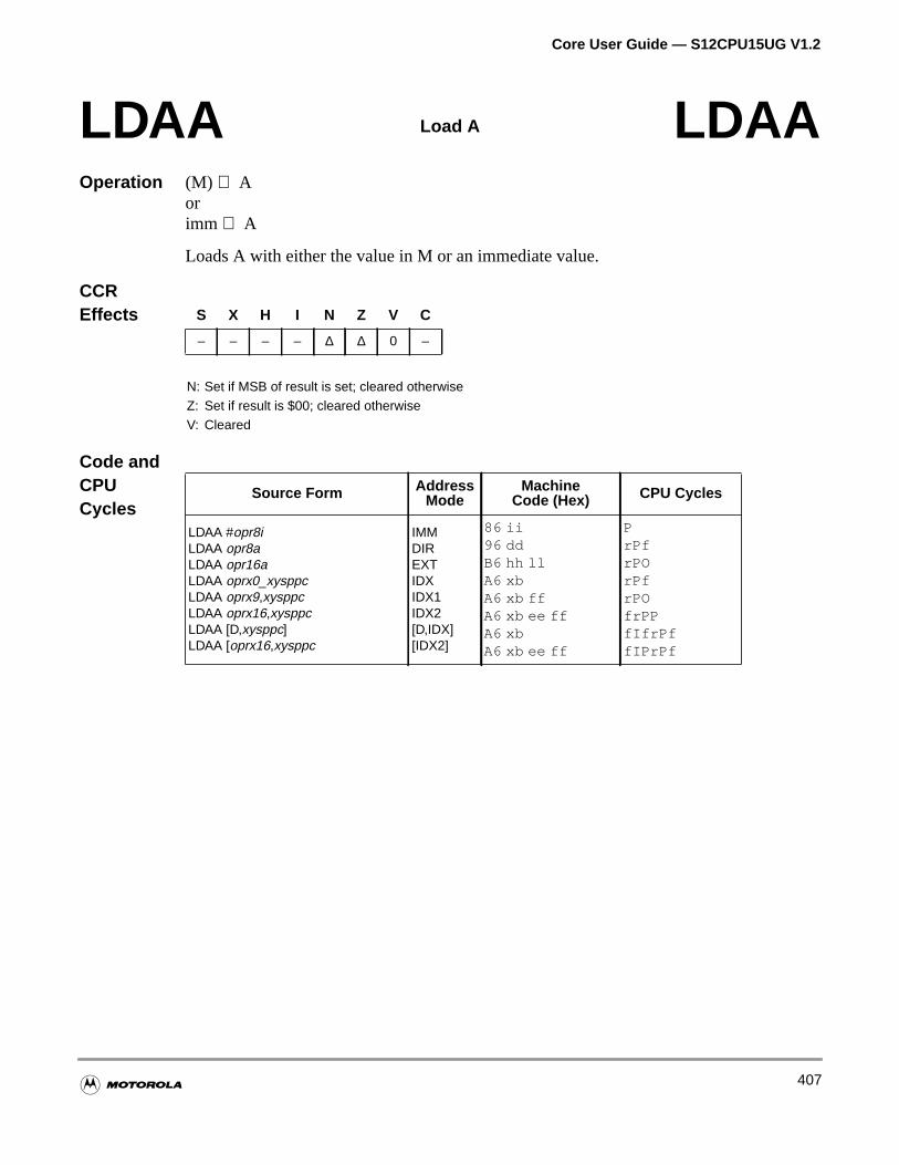
Core User Guide — S12CPU15UG V1.2
Operation (M) ⇒ Aorimm ⇒ A
Loads A with either the value in M or an immediate value.
CCREffects
Code andCPUCycles
LDAA Load A LDAA
S X H I N Z V C
– – – – ∆ ∆ 0 –
N: Set if MSB of result is set; cleared otherwiseZ: Set if result is $00; cleared otherwiseV: Cleared
Source Form AddressMode
MachineCode (Hex) CPU Cycles
LDAA #opr8iLDAA opr8aLDAA opr16aLDAA oprx0_xysppcLDAA oprx9,xysppcLDAA oprx16,xysppcLDAA [D,xysppc]LDAA [oprx16,xysppc
IMMDIREXTIDXIDX1IDX2[D,IDX][IDX2]
86 ii96 ddB6 hh llA6 xbA6 xb ffA6 xb ee ffA6 xbA6 xb ee ff
PrPfrPOrPfrPOfrPPfIfrPffIPrPf
407
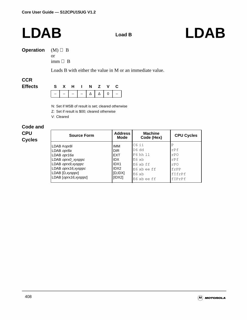
Core User Guide — S12CPU15UG V1.2
Operation (M) ⇒ Borimm ⇒ B
Loads B with either the value in M or an immediate value.
CCREffects
Code andCPUCycles
LDAB Load B LDAB
S X H I N Z V C
– – – – ∆ ∆ 0 –
N: Set if MSB of result is set; cleared otherwiseZ: Set if result is $00; cleared otherwiseV: Cleared
Source Form AddressMode
MachineCode (Hex) CPU Cycles
LDAB #opr8iLDAB opr8aLDAB opr16aLDAB oprx0_xysppcLDAB oprx9,xysppcLDAB oprx16,xysppcLDAB [D,xysppc]LDAB [oprx16,xysppc]
IMMDIREXTIDXIDX1IDX2[D,IDX][IDX2]
C6 iiD6 ddF6 hh llE6 xbE6 xb ffE6 xb ee ffE6 xbE6 xb ee ff
PrPfrPOrPfrPOfrPPfIfrPffIPrPf
408
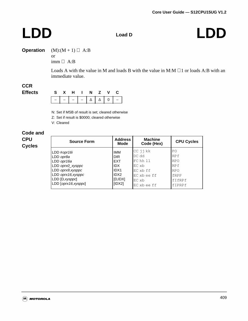
Core User Guide — S12CPU15UG V1.2
Operation (M):(M + 1) ⇒ A:Borimm ⇒ A:B
Loads A with the value in M and loads B with the value in M:M+ 1 or loads A:B with animmediate value.
CCREffects
Code andCPUCycles
LDD Load D LDD
S X H I N Z V C
– – – – ∆ ∆ 0 –
N: Set if MSB of result is set; cleared otherwiseZ: Set if result is $0000; cleared otherwiseV: Cleared
Source Form AddressMode
MachineCode (Hex) CPU Cycles
LDD #opr16iLDD opr8aLDD opr16aLDD oprx0_xysppcLDD oprx9,xysppcLDD oprx16,xysppcLDD [D,xysppc]LDD [oprx16,xysppc]
IMMDIREXTIDXIDX1IDX2[D,IDX][IDX2]
CC jj kkDC ddFC hh llEC xbEC xb ffEC xb ee ffEC xbEC xb ee ff
PORPfRPORPfRPOfRPPfIfRPffIPRPf
409
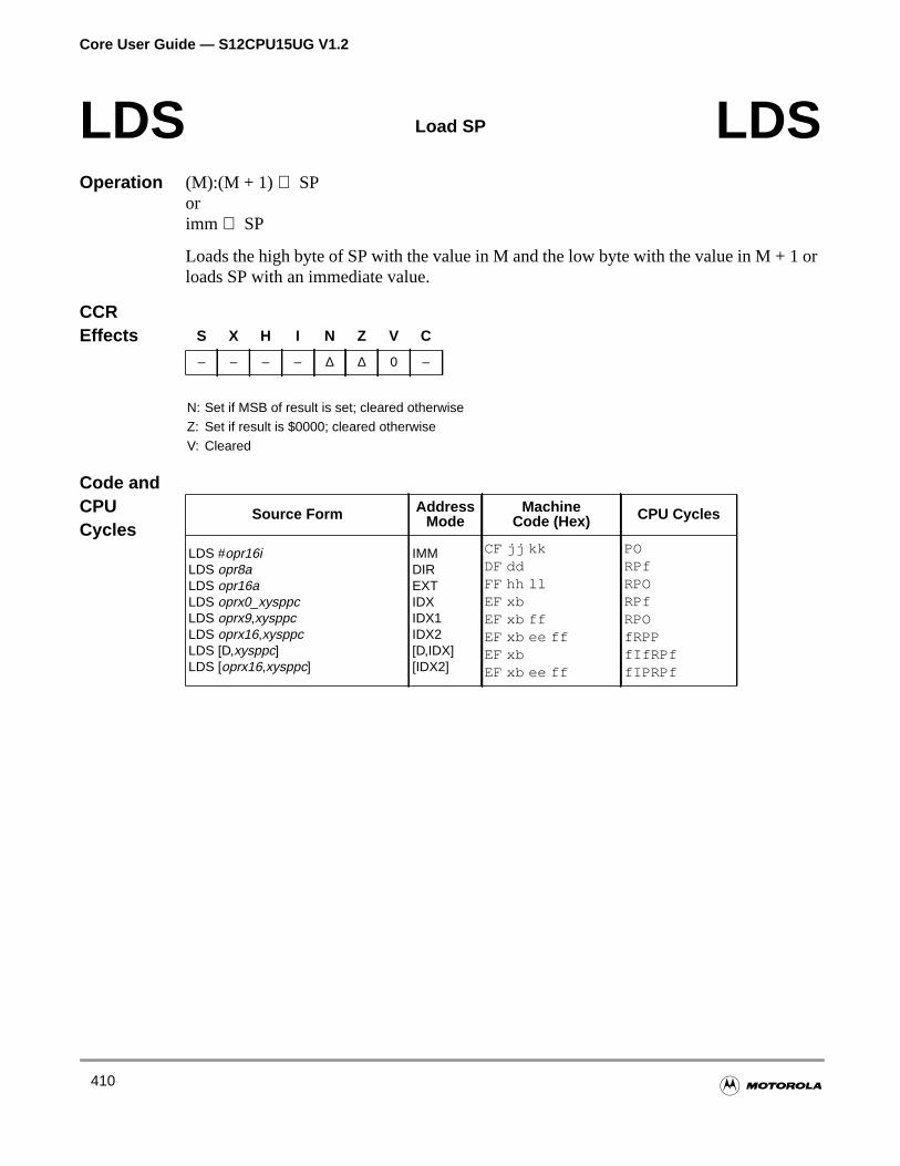
Core User Guide — S12CPU15UG V1.2
or
Operation (M):(M + 1) ⇒ SPorimm ⇒ SP
Loads the high byte of SP with the value in M and the low byte with the value in M + 1loads SP with an immediate value.
CCREffects
Code andCPUCycles
LDS Load SP LDS
S X H I N Z V C
– – – – ∆ ∆ 0 –
N: Set if MSB of result is set; cleared otherwiseZ: Set if result is $0000; cleared otherwiseV: Cleared
Source Form AddressMode
MachineCode (Hex) CPU Cycles
LDS #opr16iLDS opr8aLDS opr16aLDS oprx0_xysppcLDS oprx9,xysppcLDS oprx16,xysppcLDS [D,xysppc]LDS [oprx16,xysppc]
IMMDIREXTIDXIDX1IDX2[D,IDX][IDX2]
CF jj kkDF ddFF hh llEF xbEF xb ffEF xb ee ffEF xbEF xb ee ff
PORPfRPORPfRPOfRPPfIfRPffIPRPf
410

Core User Guide — S12CPU15UG V1.2
X
Operation (M):(M + 1) ⇒ Xorimm ⇒ X
Loads the high byte of X with value in M and low byte with the value in M + 1 or loadswith an immediate value.
CCREffects
Code andCPUCycles
LDX Load X LDX
S X H I N Z V C
– – – – ∆ ∆ 0 –
N: Set if MSB of result is set; cleared otherwiseZ: Set if result is $0000; cleared otherwiseV: Cleared
Source Form AddressMode
MachineCode (Hex) CPU Cycles
LDX #opr16iLDX opr8aLDX opr16aLDX oprx0_xysppcLDX oprx9,xysppcLDX oprx16,xysppcLDX [D,xysppc]LDX [oprx16,xysppc]
IMMDIREXTIDXIDX1IDX2[D,IDX][IDX2]
CE jj kkDE ddFE hh llEE xbEE xb ffEE xb ee ffEE xbEE xb ee ff
PORPfRPORPfRPOfRPPfIfRPffIPRPf
411

Core User Guide — S12CPU15UG V1.2
or
Operation (M):(M + 1) ⇒ Yorimm ⇒ Y
Loads the high byte of Y with the value in M and the low byte with the value in M + 1loads Y with an immediate value.
CCREffects
Code andCPUCycles
LDY Load Y LDY
S X H I N Z V C
– – – – ∆ ∆ 0 –
N: Set if MSB of result is set; cleared otherwiseZ: Set if result is $0000; cleared otherwiseV: Cleared
Source Form AddressMode
MachineCode (Hex) CPU Cycles
LDY #opr16iLDY opr8aLDY opr16aLDY oprx0_xysppcLDY oprx9,xysppcLDY oprx16,xysppcLDY [D,xysppc]LDY [oprx16,xysppc]
IMMDIREXTIDXIDX1IDX2[D,IDX][IDX2]
CD jj kkDD ddFD hh llED xbED xb ffED xb ee ffED xbED xb ee ff
PORPfRPORPfRPOfRPPfIfRPffIPRPf
412
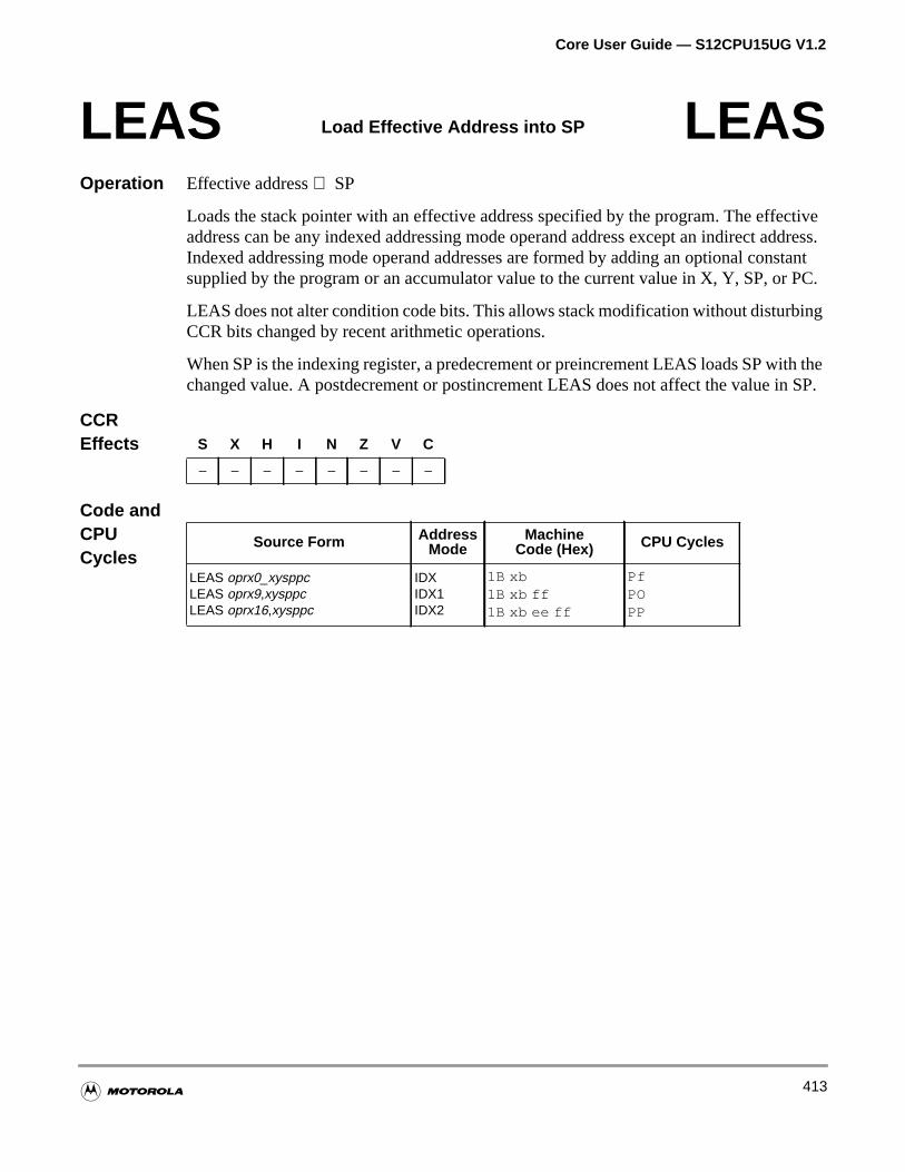
Core User Guide — S12CPU15UG V1.2
ctiveddress.stant PC.
ing
th then SP.
Operation Effective address⇒ SP
Loads the stack pointer with an effective address specified by the program. The effeaddress can be any indexed addressing mode operand address except an indirect aIndexed addressing mode operand addresses are formed by adding an optional consupplied by the program or an accumulator value to the current value in X, Y, SP, or
LEAS does not alter condition code bits. This allows stack modification without disturbCCR bits changed by recent arithmetic operations.
When SP is the indexing register, a predecrement or preincrement LEAS loads SP wichanged value. A postdecrement or postincrement LEAS does not affect the value i
CCREffects
Code andCPUCycles
LEAS Load Effective Address into SP LEAS
S X H I N Z V C
– – – – – – – –
Source Form AddressMode
MachineCode (Hex) CPU Cycles
LEAS oprx0_xysppcLEAS oprx9,xysppcLEAS oprx16,xysppc
IDXIDX1IDX2
1B xb1B xb ff1B xb ee ff
PfPOPP
413
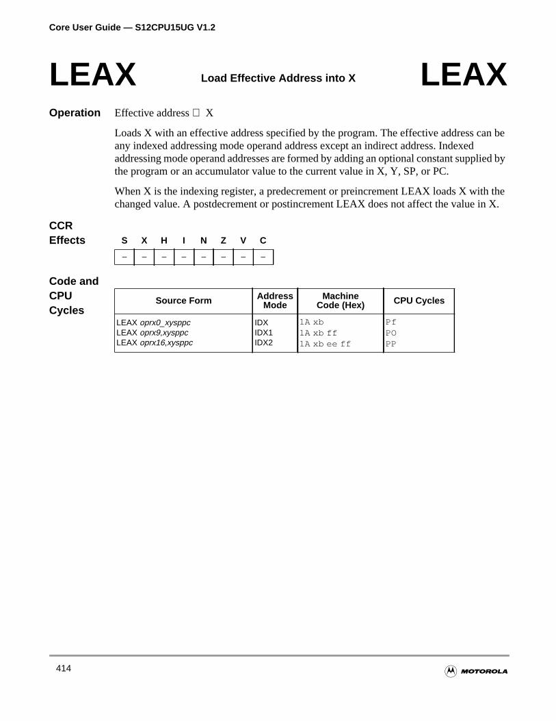
Core User Guide — S12CPU15UG V1.2
an be
lied by
then X.
Operation Effective address⇒ X
Loads X with an effective address specified by the program. The effective address cany indexed addressing mode operand address except an indirect address. Indexedaddressing mode operand addresses are formed by adding an optional constant suppthe program or an accumulator value to the current value in X, Y, SP, or PC.
When X is the indexing register, a predecrement or preincrement LEAX loads X withchanged value. A postdecrement or postincrement LEAX does not affect the value i
CCREffects
Code andCPUCycles
LEAX Load Effective Address into X LEAX
S X H I N Z V C
– – – – – – – –
Source Form AddressMode
MachineCode (Hex) CPU Cycles
LEAX oprx0_xysppcLEAX oprx9,xysppcLEAX oprx16,xysppc
IDXIDX1IDX2
1A xb1A xb ff1A xb ee ff
PfPOPP
414
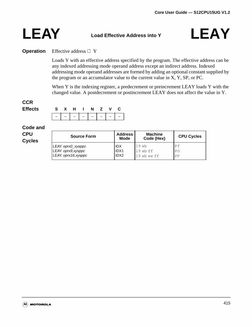
Core User Guide — S12CPU15UG V1.2
an be
lied by
then Y.
Operation Effective address⇒ Y
Loads Y with an effective address specified by the program. The effective address cany indexed addressing mode operand address except an indirect address. Indexedaddressing mode operand addresses are formed by adding an optional constant suppthe program or an accumulator value to the current value in X, Y, SP, or PC.
When Y is the indexing register, a predecrement or preincrement LEAY loads Y withchanged value. A postdecrement or postincrement LEAY does not affect the value i
CCREffects
Code andCPUCycles
LEAY Load Effective Address into Y LEAY
S X H I N Z V C
– – – – – – – –
Source Form AddressMode
MachineCode (Hex) CPU Cycles
LEAY oprx0_xysppcLEAY oprx9,xysppcLEAY oprx16,xysppc
IDXIDX1IDX2
19 xb19 xb ff19 xb ee ff
PfPOPP
415

Core User Guide — S12CPU15UG V1.2
he
Operation
Shifts all bits of the M one place to the left. Loads bit 0 with 0. Loads the C bit from tmost significant bit of M.
CCREffects
Code andCPUCycles
LSL Logical Shift Left M(same as ASL) LSL
b7 b6 b5 b4 b3 b2 b1 b0C 0
M
S X H I N Z V C
– – – – ∆ ∆ ∆ ∆
N: Set if MSB of result is set; cleared otherwiseZ: Set if result is $00; cleared otherwiseV: N ⊕ C = [N • C] | [N • C] (for N and C after the shift); set if (N is set and C is cleared) or (N is cleared and
C is set); cleared otherwise (for values of N and C after the shift)C: M7; set if the LSB of M was set before the shift; cleared otherwise
Source Form AddressMode
MachineCode (Hex) CPU Cycles
LSL opr16aLSL oprx0_xysppcLSL oprx9,xysppcLSL oprx16,xysppcLSL [D,xysppc]LSL [oprx16,xysppc]
EXTIDXIDX1IDX2[D,IDX][IDX2]
78 hh ll68 xb68 xb ff68 xb ee ff68 xb68 xb ee ff
rPwOrPwrPwOfrPPwfIfrPwfIPrPw
416
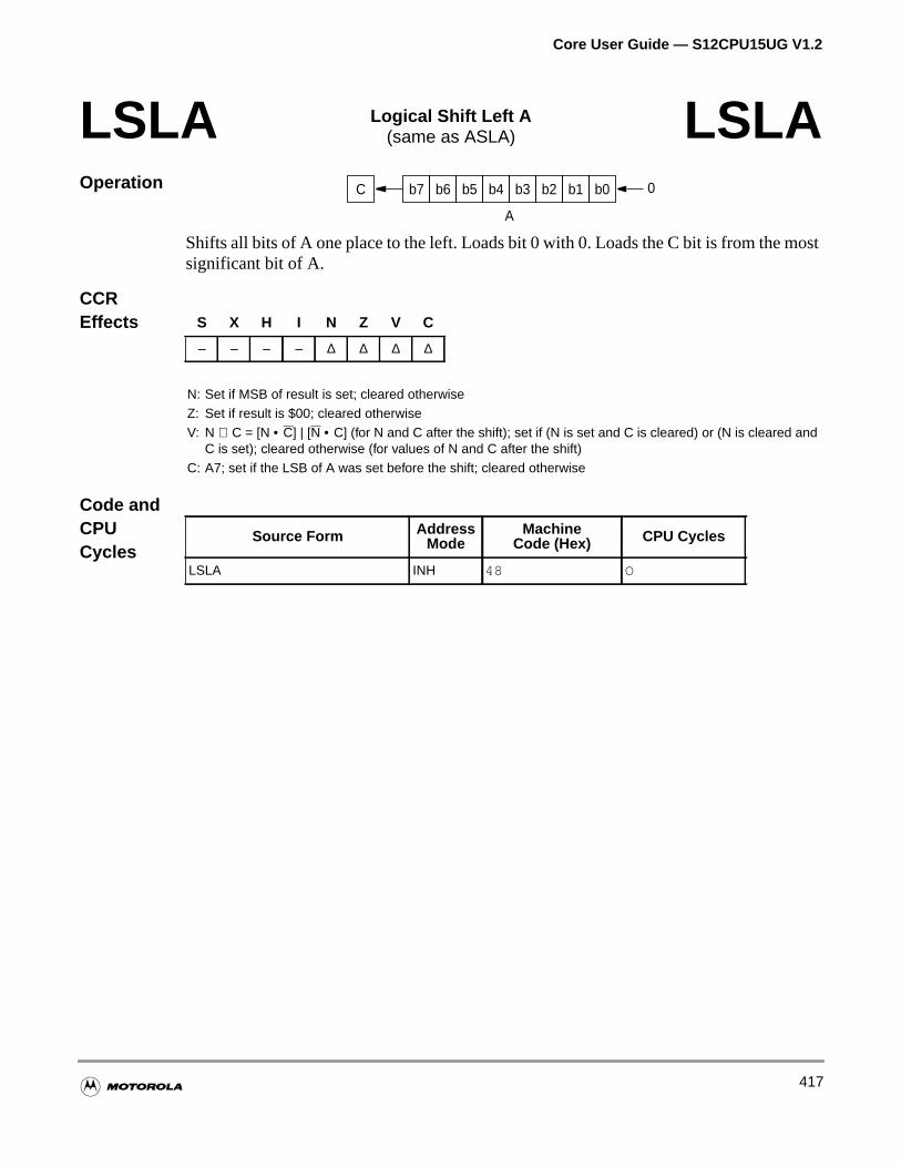
Core User Guide — S12CPU15UG V1.2
ost
Operation
Shifts all bits of A one place to the left. Loads bit 0 with 0. Loads the C bit is from the msignificant bit of A.
CCREffects
Code andCPUCycles
LSLA Logical Shift Left A(same as ASLA) LSLA
b7 b6 b5 b4 b3 b2 b1 b0C 0
A
S X H I N Z V C
– – – – ∆ ∆ ∆ ∆
N: Set if MSB of result is set; cleared otherwiseZ: Set if result is $00; cleared otherwiseV: N ⊕ C = [N • C] | [N • C] (for N and C after the shift); set if (N is set and C is cleared) or (N is cleared and
C is set); cleared otherwise (for values of N and C after the shift)C: A7; set if the LSB of A was set before the shift; cleared otherwise
Source Form AddressMode
MachineCode (Hex) CPU Cycles
LSLA INH 48 O
417
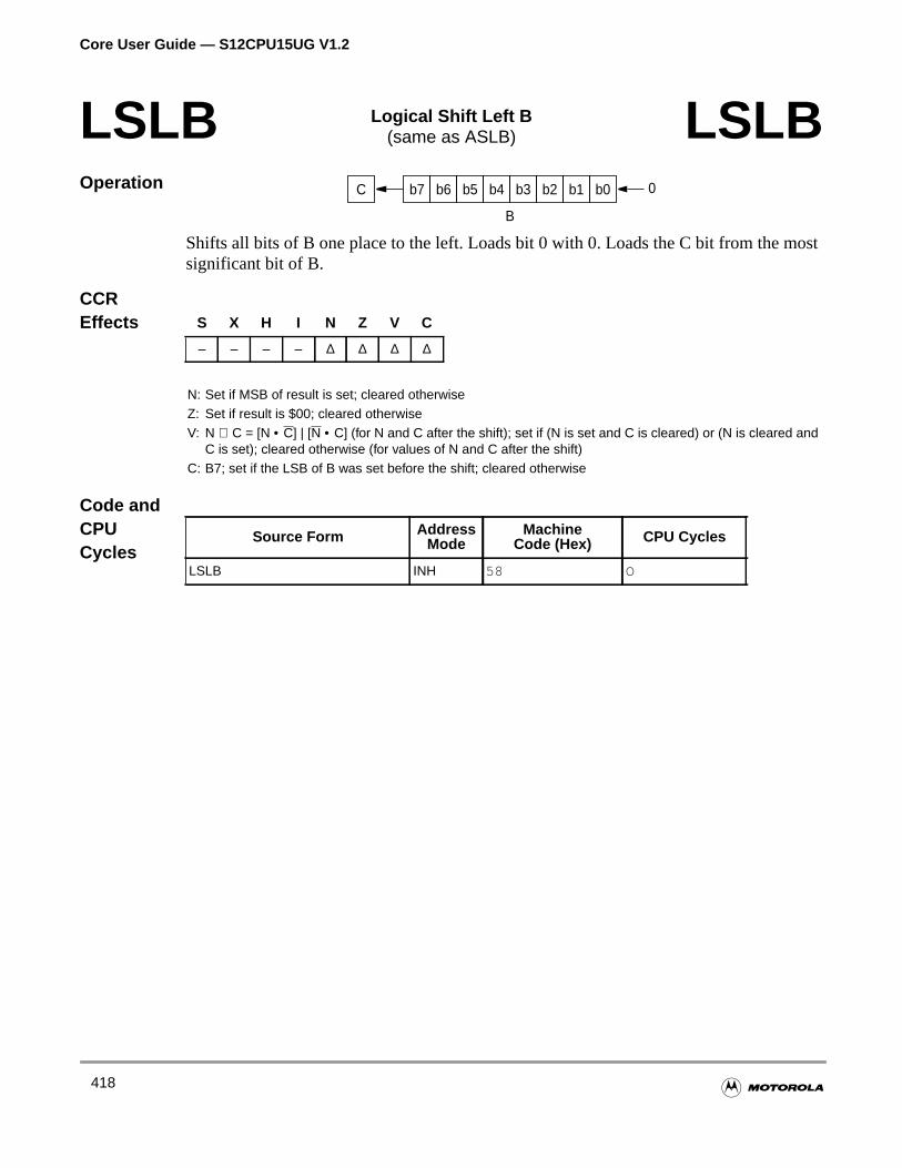
Core User Guide — S12CPU15UG V1.2
ost
Operation
Shifts all bits of B one place to the left. Loads bit 0 with 0. Loads the C bit from the msignificant bit of B.
CCREffects
Code andCPUCycles
LSLB Logical Shift Left B(same as ASLB) LSLB
b7 b6 b5 b4 b3 b2 b1 b0C 0
B
S X H I N Z V C
– – – – ∆ ∆ ∆ ∆
N: Set if MSB of result is set; cleared otherwiseZ: Set if result is $00; cleared otherwiseV: N ⊕ C = [N • C] | [N • C] (for N and C after the shift); set if (N is set and C is cleared) or (N is cleared and
C is set); cleared otherwise (for values of N and C after the shift)C: B7; set if the LSB of B was set before the shift; cleared otherwise
Source Form AddressMode
MachineCode (Hex) CPU Cycles
LSLB INH 58 O
418
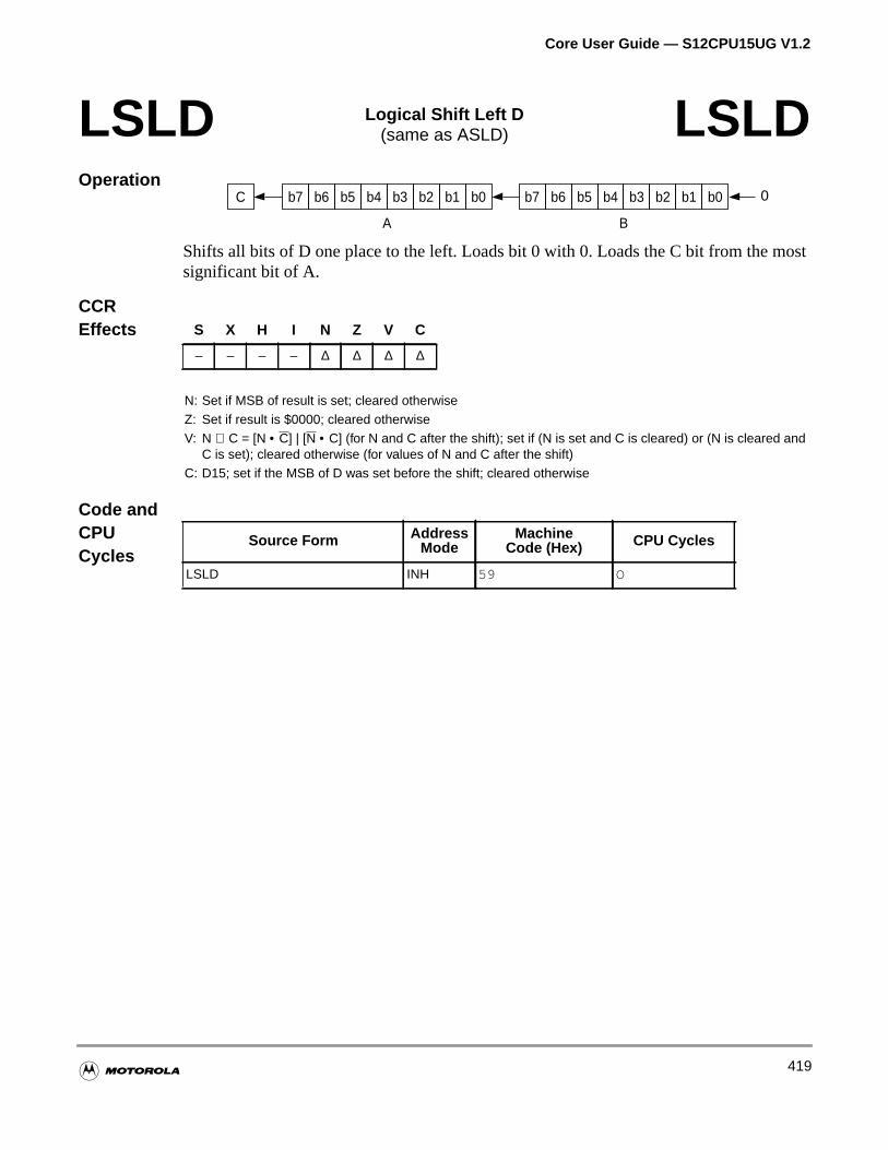
Core User Guide — S12CPU15UG V1.2
ost
Operation
Shifts all bits of D one place to the left. Loads bit 0 with 0. Loads the C bit from the msignificant bit of A.
CCREffects
Code andCPUCycles
LSLD Logical Shift Left D(same as ASLD) LSLD
0b7 b6 b5 b4 b3 b2 b1 b0 b7 b6 b5 b4 b3 b2 b1 b0C
BA
S X H I N Z V C
– – – – ∆ ∆ ∆ ∆
N: Set if MSB of result is set; cleared otherwiseZ: Set if result is $0000; cleared otherwiseV: N ⊕ C = [N • C] | [N • C] (for N and C after the shift); set if (N is set and C is cleared) or (N is cleared and
C is set); cleared otherwise (for values of N and C after the shift)C: D15; set if the MSB of D was set before the shift; cleared otherwise
Source Form AddressMode
MachineCode (Hex) CPU Cycles
LSLD INH 59 O
419
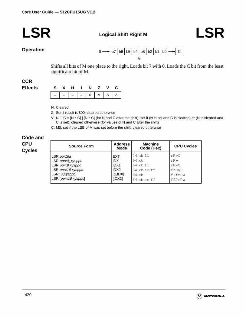
Core User Guide — S12CPU15UG V1.2
ast
Operation
Shifts all bits of M one place to the right. Loads bit 7 with 0. Loads the C bit from the lesignificant bit of M.
CCREffects
Code andCPUCycles
LSR Logical Shift Right M LSRb7 b6 b5 b4 b3 b2 b1 b00
M
C
S X H I N Z V C
– – – – 0 ∆ ∆ ∆
N: ClearedZ: Set if result is $00; cleared otherwiseV: N ⊕ C = [N • C] | [N • C] (for N and C after the shift); set if (N is set and C is cleared) or (N is cleared and
C is set); cleared otherwise (for values of N and C after the shift)C: M0; set if the LSB of M was set before the shift; cleared otherwise
Source Form AddressMode
MachineCode (Hex) CPU Cycles
LSR opr16aLSR oprx0_xysppcLSR oprx9,xysppcLSR oprx16,xysppcLSR [D,xysppc]LSR [oprx16,xysppc]
EXTIDXIDX1IDX2[D,IDX][IDX2]
74 hh ll64 xb64 xb ff64 xb ee ff64 xb64 xb ee ff
rPwOrPwrPwOfrPwPfIfrPwfIPrPw
420
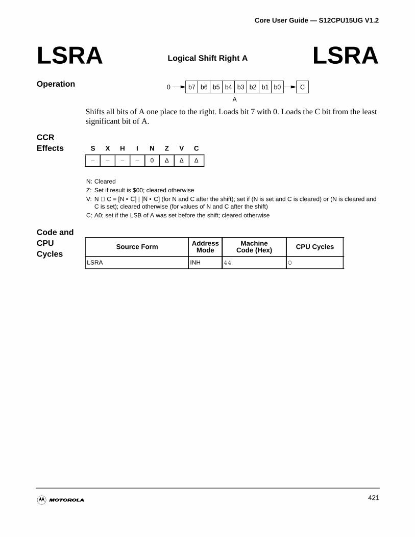
Core User Guide — S12CPU15UG V1.2
ast
Operation
Shifts all bits of A one place to the right. Loads bit 7 with 0. Loads the C bit from the lesignificant bit of A.
CCREffects
Code andCPUCycles
LSRA Logical Shift Right A LSRAb7 b6 b5 b4 b3 b2 b1 b00
A
C
S X H I N Z V C
– – – – 0 ∆ ∆ ∆
N: ClearedZ: Set if result is $00; cleared otherwiseV: N ⊕ C = [N • C] | [N • C] (for N and C after the shift); set if (N is set and C is cleared) or (N is cleared and
C is set); cleared otherwise (for values of N and C after the shift)C: A0; set if the LSB of A was set before the shift; cleared otherwise
Source Form AddressMode
MachineCode (Hex) CPU Cycles
LSRA INH 44 O
421
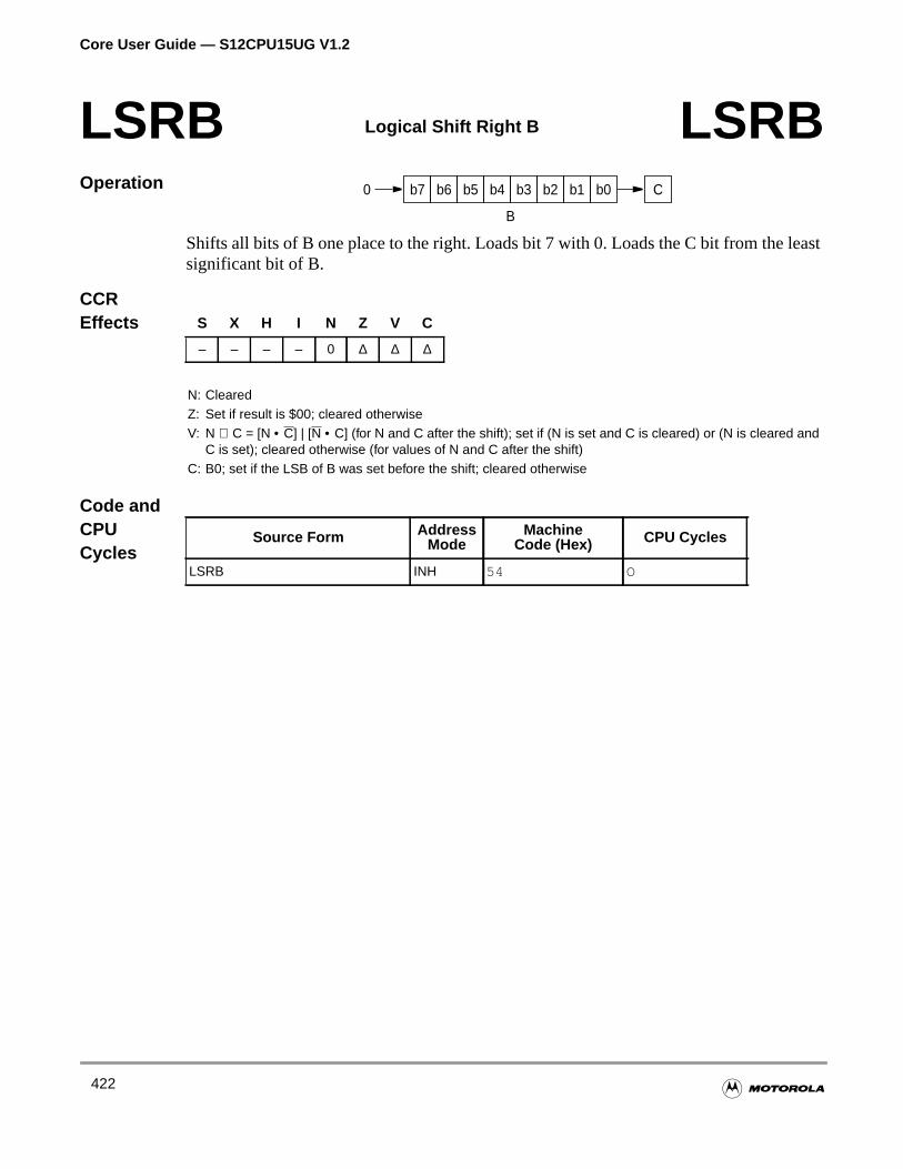
Core User Guide — S12CPU15UG V1.2
ast
Operation
Shifts all bits of B one place to the right. Loads bit 7 with 0. Loads the C bit from the lesignificant bit of B.
CCREffects
Code andCPUCycles
LSRB Logical Shift Right B LSRBb7 b6 b5 b4 b3 b2 b1 b00
B
C
S X H I N Z V C
– – – – 0 ∆ ∆ ∆
N: ClearedZ: Set if result is $00; cleared otherwiseV: N ⊕ C = [N • C] | [N • C] (for N and C after the shift); set if (N is set and C is cleared) or (N is cleared and
C is set); cleared otherwise (for values of N and C after the shift)C: B0; set if the LSB of B was set before the shift; cleared otherwise
Source Form AddressMode
MachineCode (Hex) CPU Cycles
LSRB INH 54 O
422
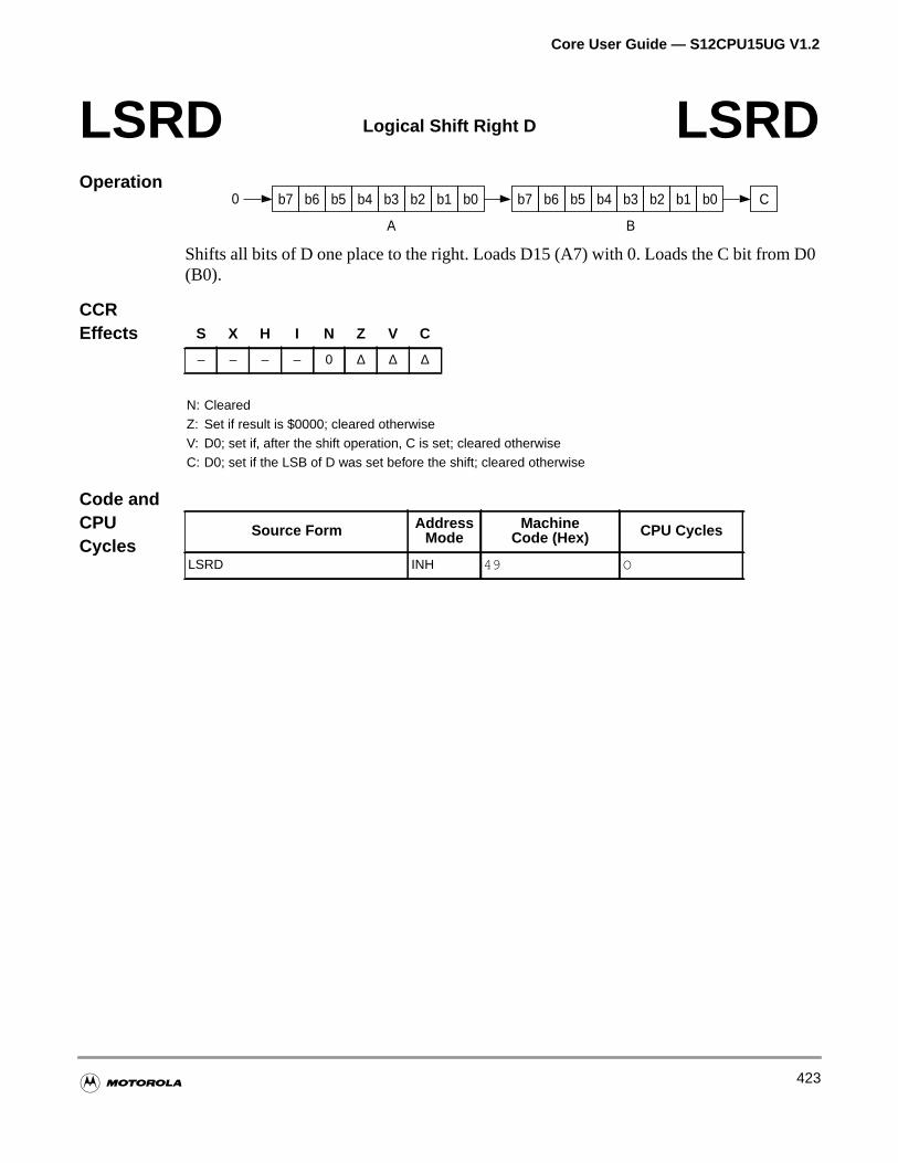
Core User Guide — S12CPU15UG V1.2
0
Operation
Shifts all bits of D one place to the right. Loads D15 (A7) with 0. Loads the C bit from D(B0).
CCREffects
Code andCPUCycles
LSRD Logical Shift Right D LSRDb7 b6 b5 b4 b3 b2 b1 b0 b7 b6 b5 b4 b3 b2 b1 b00
BA
C
S X H I N Z V C
– – – – 0 ∆ ∆ ∆
N: ClearedZ: Set if result is $0000; cleared otherwiseV: D0; set if, after the shift operation, C is set; cleared otherwiseC: D0; set if the LSB of D was set before the shift; cleared otherwise
Source Form AddressMode
MachineCode (Hex) CPU Cycles
LSRD INH 49 O
423
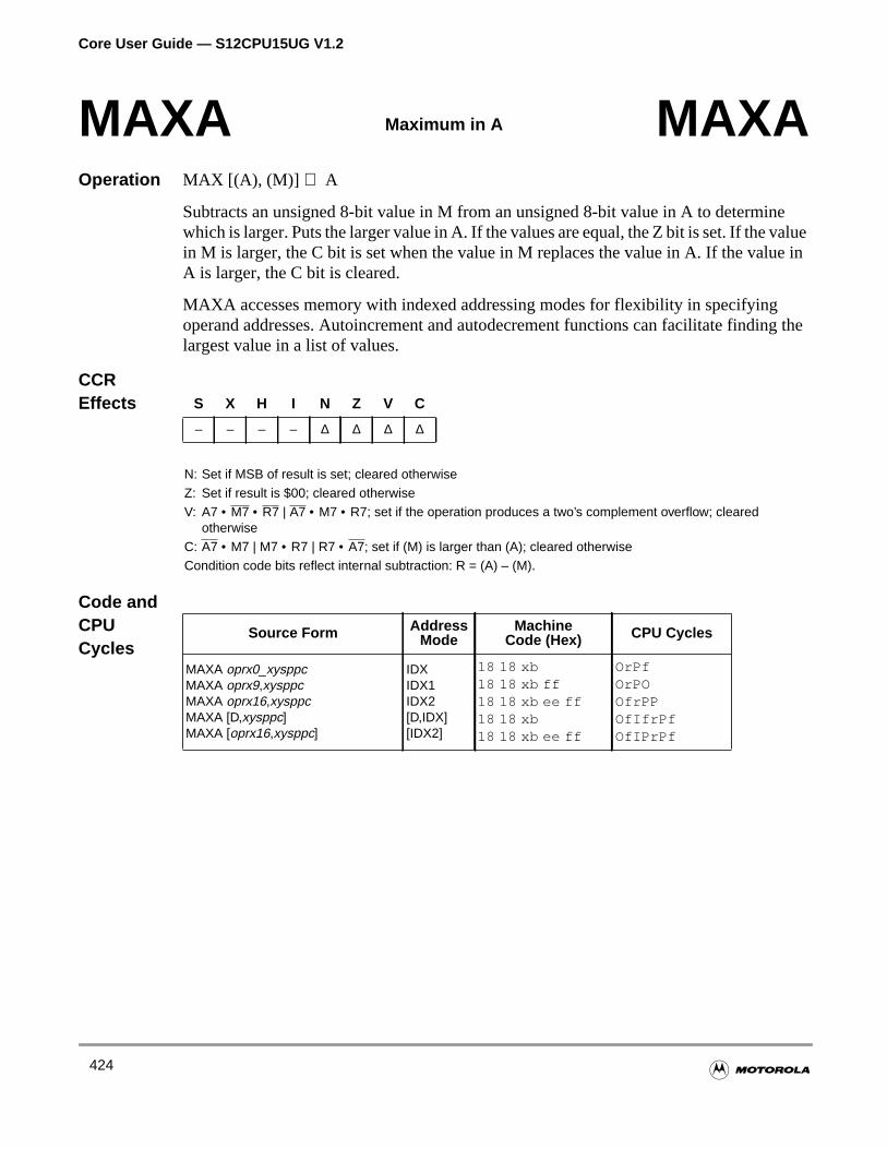
Core User Guide — S12CPU15UG V1.2
ealuee in
g the
Operation MAX [(A), (M)] ⇒ A
Subtracts an unsigned 8-bit value in M from an unsigned 8-bit value in A to determinwhich is larger. Puts the larger value in A. If the values are equal, the Z bit is set. If the vin M is larger, the C bit is set when the value in M replaces the value in A. If the valuA is larger, the C bit is cleared.
MAXA accesses memory with indexed addressing modes for flexibility in specifyingoperand addresses. Autoincrement and autodecrement functions can facilitate findinlargest value in a list of values.
CCREffects
Code andCPUCycles
MAXA Maximum in A MAXA
S X H I N Z V C
– – – – ∆ ∆ ∆ ∆
N: Set if MSB of result is set; cleared otherwiseZ: Set if result is $00; cleared otherwiseV: A7 • M7 • R7 | A7 • M7 • R7; set if the operation produces a two’s complement overflow; cleared
otherwiseC: A7 • M7 | M7 • R7 | R7 • A7; set if (M) is larger than (A); cleared otherwiseCondition code bits reflect internal subtraction: R = (A) – (M).
Source Form AddressMode
MachineCode (Hex) CPU Cycles
MAXA oprx0_xysppcMAXA oprx9,xysppcMAXA oprx16,xysppcMAXA [D,xysppc]MAXA [oprx16,xysppc]
IDXIDX1IDX2[D,IDX][IDX2]
18 18 xb18 18 xb ff18 18 xb ee ff18 18 xb18 18 xb ee ff
OrPfOrPOOfrPPOfIfrPfOfIPrPf
424
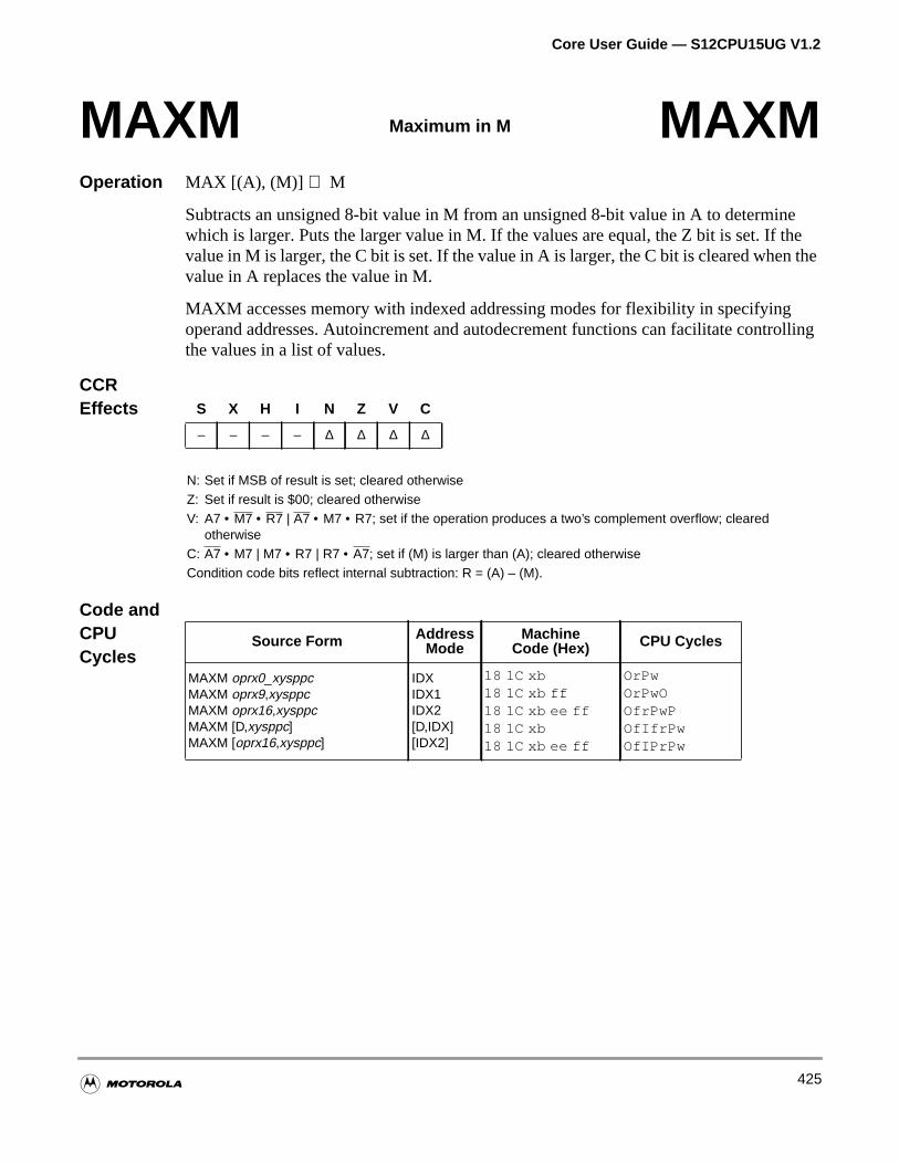
Core User Guide — S12CPU15UG V1.2
ethethe
olling
Operation MAX [(A), (M)] ⇒ M
Subtracts an unsigned 8-bit value in M from an unsigned 8-bit value in A to determinwhich is larger. Puts the larger value in M. If the values are equal, the Z bit is set. If value in M is larger, the C bit is set. If the value in A is larger, the C bit is cleared whenvalue in A replaces the value in M.
MAXM accesses memory with indexed addressing modes for flexibility in specifyingoperand addresses. Autoincrement and autodecrement functions can facilitate contrthe values in a list of values.
CCREffects
Code andCPUCycles
MAXM Maximum in M MAXM
S X H I N Z V C
– – – – ∆ ∆ ∆ ∆
N: Set if MSB of result is set; cleared otherwiseZ: Set if result is $00; cleared otherwiseV: A7 • M7 • R7 | A7 • M7 • R7; set if the operation produces a two’s complement overflow; cleared
otherwiseC: A7 • M7 | M7 • R7 | R7 • A7; set if (M) is larger than (A); cleared otherwiseCondition code bits reflect internal subtraction: R = (A) – (M).
Source Form AddressMode
MachineCode (Hex) CPU Cycles
MAXM oprx0_xysppcMAXM oprx9,xysppcMAXM oprx16,xysppcMAXM [D,xysppc]MAXM [oprx16,xysppc]
IDXIDX1IDX2[D,IDX][IDX2]
18 1C xb18 1C xb ff18 1C xb ee ff18 1C xb18 1C xb ee ff
OrPwOrPwOOfrPwPOfIfrPwOfIPrPw
425
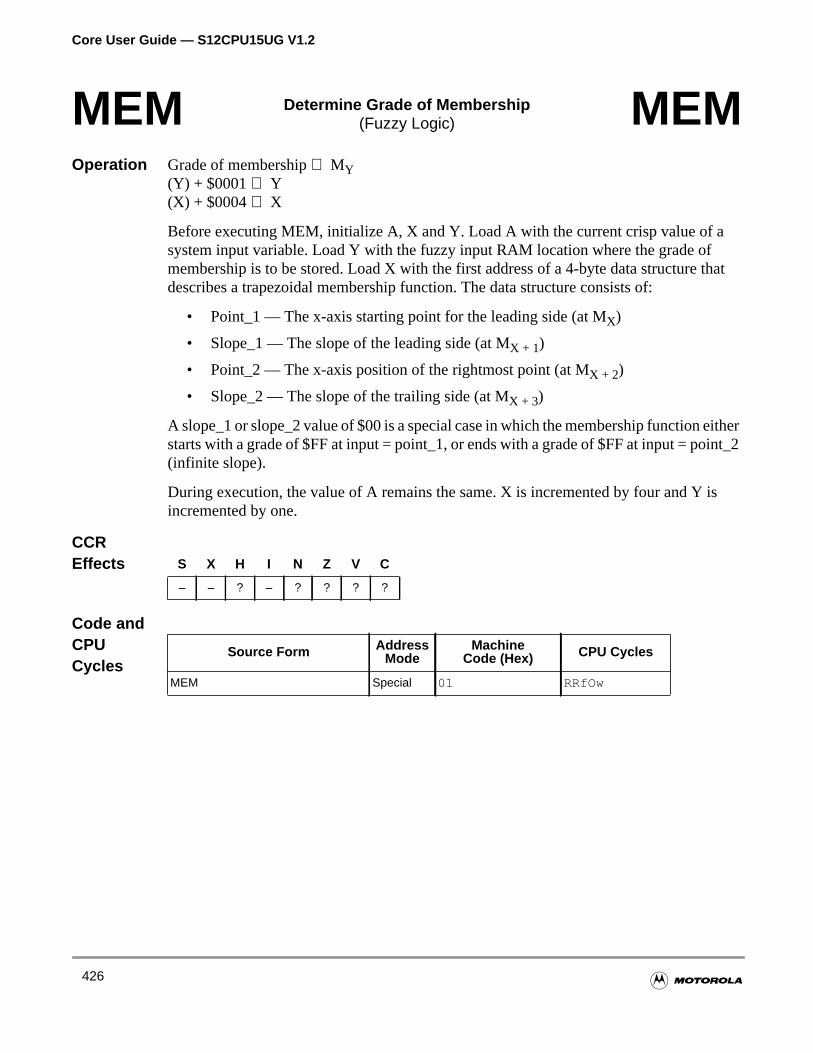
Core User Guide — S12CPU15UG V1.2
that
ithernt_2
is
Operation Grade of membership⇒ MY(Y) + $0001⇒ Y(X) + $0004⇒ X
Before executing MEM, initialize A, X and Y. Load A with the current crisp value of asystem input variable. Load Y with the fuzzy input RAM location where the grade ofmembership is to be stored. Load X with the first address of a 4-byte data structure describes a trapezoidal membership function. The data structure consists of:
• Point_1 — The x-axis starting point for the leading side (at MX)
• Slope_1 — The slope of the leading side (at MX + 1)
• Point_2 — The x-axis position of the rightmost point (at MX + 2)
• Slope_2 — The slope of the trailing side (at MX + 3)
A slope_1 or slope_2 value of $00 is a special case in which the membership function estarts with a grade of $FF at input = point_1, or ends with a grade of $FF at input = poi(infinite slope).
During execution, the value of A remains the same. X is incremented by four and Y incremented by one.
CCREffects
Code andCPUCycles
MEM Determine Grade of Membership(Fuzzy Logic) MEM
S X H I N Z V C
– – ? – ? ? ? ?
Source Form AddressMode
MachineCode (Hex) CPU Cycles
MEM Special 01 RRfOw
426
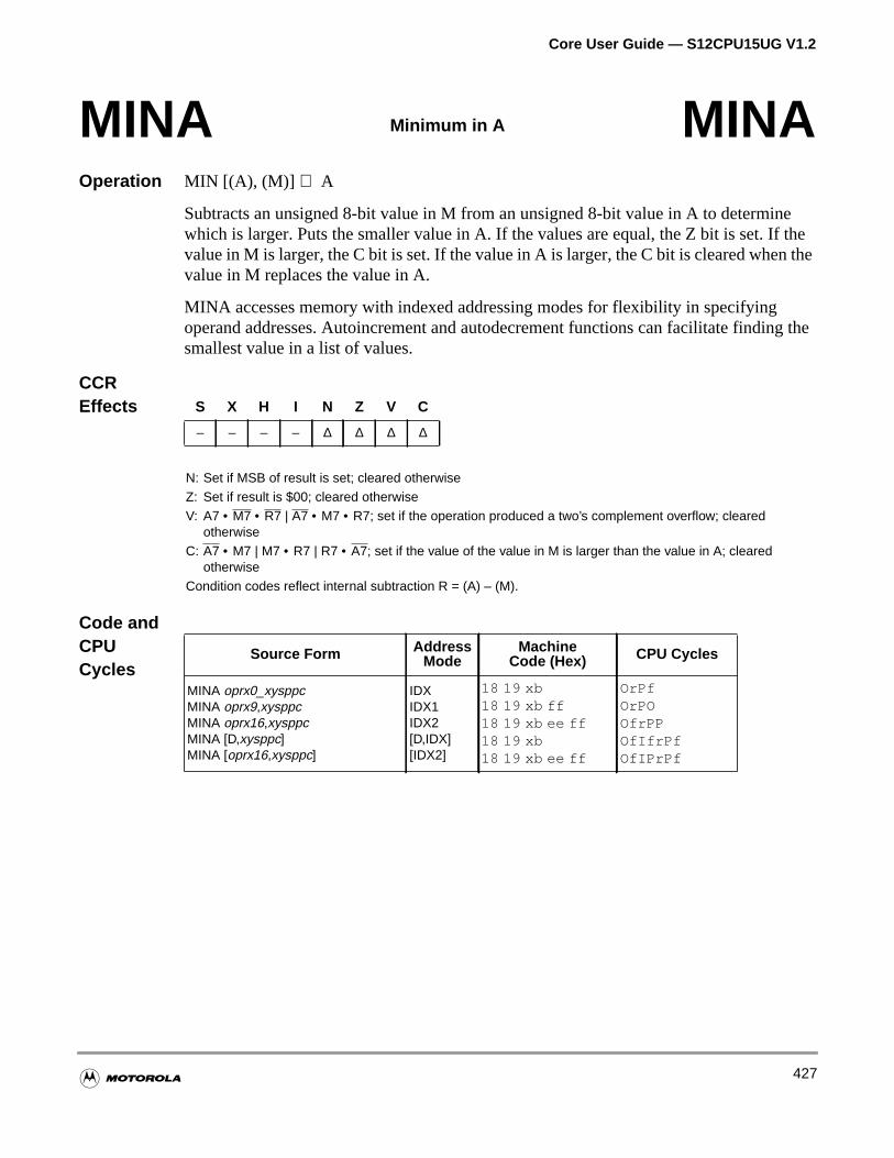
Core User Guide — S12CPU15UG V1.2
ef thethe
g the
Operation MIN [(A), (M)] ⇒ A
Subtracts an unsigned 8-bit value in M from an unsigned 8-bit value in A to determinwhich is larger. Puts the smaller value in A. If the values are equal, the Z bit is set. Ivalue in M is larger, the C bit is set. If the value in A is larger, the C bit is cleared whenvalue in M replaces the value in A.
MINA accesses memory with indexed addressing modes for flexibility in specifyingoperand addresses. Autoincrement and autodecrement functions can facilitate findinsmallest value in a list of values.
CCREffects
Code andCPUCycles
MINA Minimum in A MINA
S X H I N Z V C
– – – – ∆ ∆ ∆ ∆
N: Set if MSB of result is set; cleared otherwiseZ: Set if result is $00; cleared otherwiseV: A7 • M7 • R7 | A7 • M7 • R7; set if the operation produced a two’s complement overflow; cleared
otherwiseC: A7 • M7 | M7 • R7 | R7 • A7; set if the value of the value in M is larger than the value in A; cleared
otherwiseCondition codes reflect internal subtraction R = (A) – (M).
Source Form AddressMode
MachineCode (Hex) CPU Cycles
MINA oprx0_xysppcMINA oprx9,xysppcMINA oprx16,xysppcMINA [D,xysppc]MINA [oprx16,xysppc]
IDXIDX1IDX2[D,IDX][IDX2]
18 19 xb18 19 xb ff18 19 xb ee ff18 19 xb18 19 xb ee ff
OrPfOrPOOfrPPOfIfrPfOfIPrPf
427
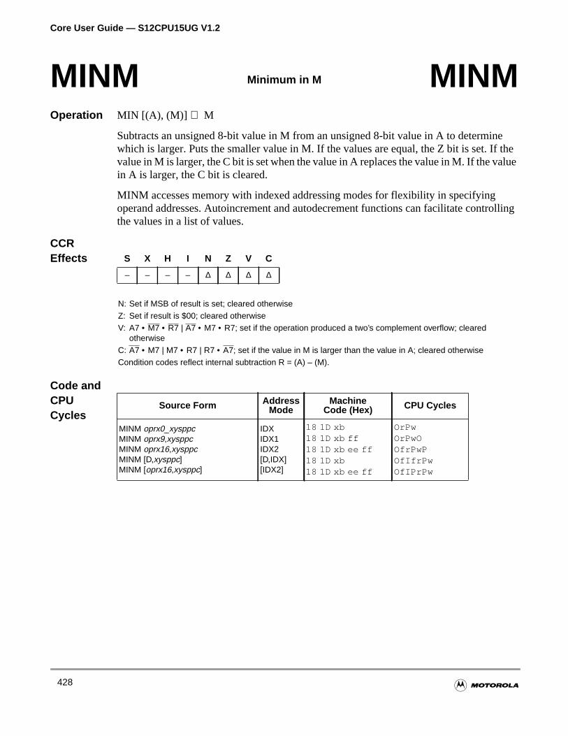
Core User Guide — S12CPU15UG V1.2
ef thelue
olling
Operation MIN [(A), (M)] ⇒ M
Subtracts an unsigned 8-bit value in M from an unsigned 8-bit value in A to determinwhich is larger. Puts the smaller value in M. If the values are equal, the Z bit is set. Ivalue in M is larger, the C bit is set when the value in A replaces the value in M. If the vain A is larger, the C bit is cleared.
MINM accesses memory with indexed addressing modes for flexibility in specifyingoperand addresses. Autoincrement and autodecrement functions can facilitate contrthe values in a list of values.
CCREffects
Code andCPUCycles
MINM Minimum in M MINM
S X H I N Z V C
– – – – ∆ ∆ ∆ ∆
N: Set if MSB of result is set; cleared otherwiseZ: Set if result is $00; cleared otherwiseV: A7 • M7 • R7 | A7 • M7 • R7; set if the operation produced a two’s complement overflow; cleared
otherwiseC: A7 • M7 | M7 • R7 | R7 • A7; set if the value in M is larger than the value in A; cleared otherwiseCondition codes reflect internal subtraction R = (A) – (M).
Source Form AddressMode
MachineCode (Hex) CPU Cycles
MINM oprx0_xysppcMINM oprx9,xysppcMINM oprx16,xysppcMINM [D,xysppc]MINM [oprx16,xysppc]
IDXIDX1IDX2[D,IDX][IDX2]
18 1D xb18 1D xb ff18 1D xb ee ff18 1D xb18 1D xb ee ff
OrPwOrPwOOfrPwPOfIfrPwOfIPrPw
428
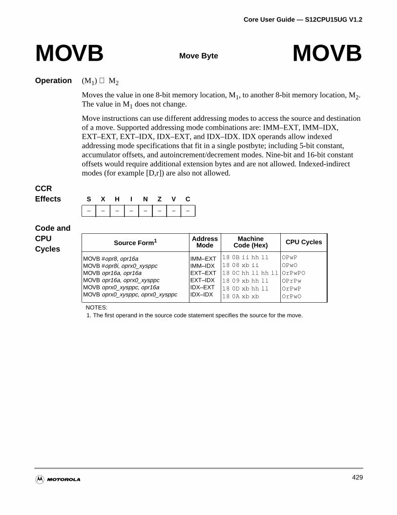
Core User Guide — S12CPU15UG V1.2
ination
tantct
Operation (M1) ⇒ M2
Moves the value in one 8-bit memory location, M1, to another 8-bit memory location, M2.The value in M1 does not change.
Move instructions can use different addressing modes to access the source and destof a move. Supported addressing mode combinations are: IMM–EXT, IMM–IDX,EXT–EXT, EXT–IDX, IDX–EXT, and IDX–IDX. IDX operands allow indexedaddressing mode specifications that fit in a single postbyte; including 5-bit constant,accumulator offsets, and autoincrement/decrement modes. Nine-bit and 16-bit consoffsets would require additional extension bytes and are not allowed. Indexed-indiremodes (for example [D,r]) are also not allowed.
CCREffects
Code andCPUCycles
MOVB Move Byte MOVB
S X H I N Z V C
– – – – – – – –
Source Form 1
NOTES:1. The first operand in the source code statement specifies the source for the move.
AddressMode
MachineCode (Hex) CPU Cycles
MOVB #opr8, opr16aMOVB #opr8i, oprx0_xysppcMOVB opr16a, opr16aMOVB opr16a, oprx0_xysppcMOVB oprx0_xysppc, opr16aMOVB oprx0_xysppc, oprx0_xysppc
IMM–EXTIMM–IDXEXT–EXTEXT–IDXIDX–EXTIDX–IDX
18 0B ii hh ll18 08 xb ii18 0C hh ll hh ll18 09 xb hh ll18 0D xb hh ll18 0A xb xb
OPwPOPwOOrPwPOOPrPwOrPwPOrPwO
429
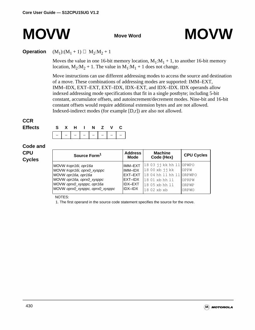
Core User Guide — S12CPU15UG V1.2
ination
6-bit
Operation (M1):(M1 + 1)⇒ M2:M2 + 1
Moves the value in one 16-bit memory location, M1:M1 + 1, to another 16-bit memorylocation, M2:M2 + 1. The value in M1:M1 + 1 does not change.
Move instructions can use different addressing modes to access the source and destof a move. These combinations of addressing modes are supported: IMM–EXT,IMM–IDX, EXT–EXT, EXT–IDX, IDX–EXT, and IDX–IDX. IDX operands allowindexed addressing mode specifications that fit in a single postbyte; including 5-bitconstant, accumulator offsets, and autoincrement/decrement modes. Nine-bit and 1constant offsets would require additional extension bytes and are not allowed.Indexed-indirect modes (for example [D,r]) are also not allowed.
CCREffects
Code andCPUCycles
MOVW Move Word MOVW
S X H I N Z V C
– – – – – – – –
Source Form 1
NOTES:1. The first operand in the source code statement specifies the source for the move.
AddressMode
MachineCode (Hex) CPU Cycles
MOVW #opr16i, opr16aMOVW #opr16i, oprx0_xysppcMOVW opr16a, opr16aMOVW opr16a, oprx0_xysppcMOVW oprx0_xysppc, opr16aMOVW oprx0_xysppc, oprx0_xysppc
IMM–EXTIMM–IDXEXT–EXTEXT–IDXIDX–EXTIDX–IDX
18 03 jj kk hh ll18 00 xb jj kk18 04 hh ll hh ll18 01 xb hh ll18 05 xb hh ll18 02 xb xb
OPWPOOPPWORPWPOOPRPWORPWPORPWO
430
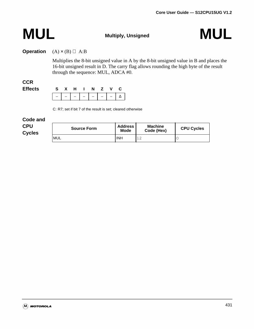
Core User Guide — S12CPU15UG V1.2
he
Operation (A) × (B) ⇒ A:B
Multiplies the 8-bit unsigned value in A by the 8-bit unsigned value in B and places t16-bit unsigned result in D. The carry flag allows rounding the high byte of the resultthrough the sequence: MUL, ADCA #0.
CCREffects
Code andCPUCycles
MUL Multiply, Unsigned MUL
S X H I N Z V C
– – – – – – – ∆
C: R7; set if bit 7 of the result is set; cleared otherwise
Source Form AddressMode
MachineCode (Hex) CPU Cycles
MUL INH 12 O
431
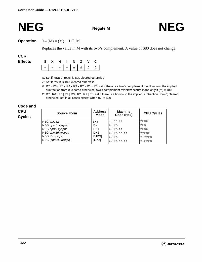
Core User Guide — S12CPU15UG V1.2
.
Operation 0 – (M) = (M) + 1 ⇒ M
Replaces the value in M with its two’s complement. A value of $80 does not change
CCREffects
Code andCPUCycles
NEG Negate M NEG
S X H I N Z V C
– – – – ∆ ∆ ∆ ∆
N: Set if MSB of result is set; cleared otherwiseZ: Set if result is $00; cleared otherwiseV: R7 • R6 • R5 • R4 • R3 • R2 • R1 • R0; set if there is a two’s complement overflow from the implied
subtraction from 0; cleared otherwise; two’s complement overflow occurs if and only if (M) = $80C: R7 | R6 | R5 | R4 | R3 | R2 | R1 | R0; set if there is a borrow in the implied subtraction from 0; cleared
otherwise; set in all cases except when (M) = $00
Source Form AddressMode
MachineCode (Hex) CPU Cycles
NEG opr16aNEG oprx0_xysppcNEG oprx9,xysppcNEG oprx16,xysppcNEG [D,xysppc]NEG [oprx16,xysppc]
EXTIDXIDX1IDX2[D,IDX][IDX2]
70 hh ll60 xb60 xb ff60 xb ee ff60 xb60 xb ee ff
rPwOrPwrPwOfrPwPfIfrPwfIPrPw
432
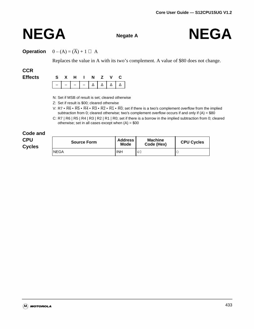
Core User Guide — S12CPU15UG V1.2
Operation 0 – (A) = (A) + 1 ⇒ A
Replaces the value in A with its two’s complement. A value of $80 does not change.
CCREffects
Code andCPUCycles
NEGA Negate A NEGA
S X H I N Z V C
– – – – ∆ ∆ ∆ ∆
N: Set if MSB of result is set; cleared otherwiseZ: Set if result is $00; cleared otherwiseV: R7 • R6 • R5 • R4 • R3 • R2 • R1 • R0; set if there is a two’s complement overflow from the implied
subtraction from 0; cleared otherwise; two’s complement overflow occurs if and only if (A) = $80C: R7 | R6 | R5 | R4 | R3 | R2 | R1 | R0; set if there is a borrow in the implied subtraction from 0; cleared
otherwise; set in all cases except when (A) = $00
Source Form AddressMode
MachineCode (Hex) CPU Cycles
NEGA INH 40 O
433

Core User Guide — S12CPU15UG V1.2
Operation 0 – (B) = (B) + 1⇒ B
Replaces the value in B with its two’s complement. A value of $80 does not change.
CCREffects
Code andCPUCycles
NEGB Negate B NEGB
S X H I N Z V C
– – – – ∆ ∆ ∆ ∆
N: Set if MSB of result is set; cleared otherwiseZ: Set if result is $00; cleared otherwiseV: R7 • R6 • R5 • R4 • R3 • R2 • R1 • R0; set if there is a two’s complement overflow from the implied
subtraction from 0; cleared otherwise; two’s complement overflow occurs if and only if (B) = $80C: R7 | R6 | R5 | R4 | R3 | R2 | R1 | R0; set if there is a borrow in the implied subtraction from 0; cleared
otherwise; set in all cases except when (B) = $00
Source Form AddressMode
MachineCode (Hex) CPU Cycles
NEGB INH 50 O
434
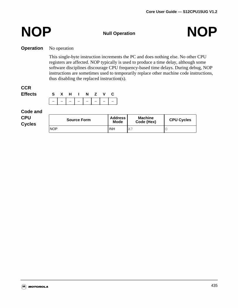
Core User Guide — S12CPU15UG V1.2
OPions,
Operation No operation
This single-byte instruction increments the PC and does nothing else. No other CPUregisters are affected. NOP typically is used to produce a time delay, although somesoftware disciplines discourage CPU frequency-based time delays. During debug, Ninstructions are sometimes used to temporarily replace other machine code instructthus disabling the replaced instruction(s).
CCREffects
Code andCPUCycles
NOP Null Operation NOP
S X H I N Z V C
– – – – – – – –
Source Form AddressMode
MachineCode (Hex) CPU Cycles
NOP INH A7 O
435
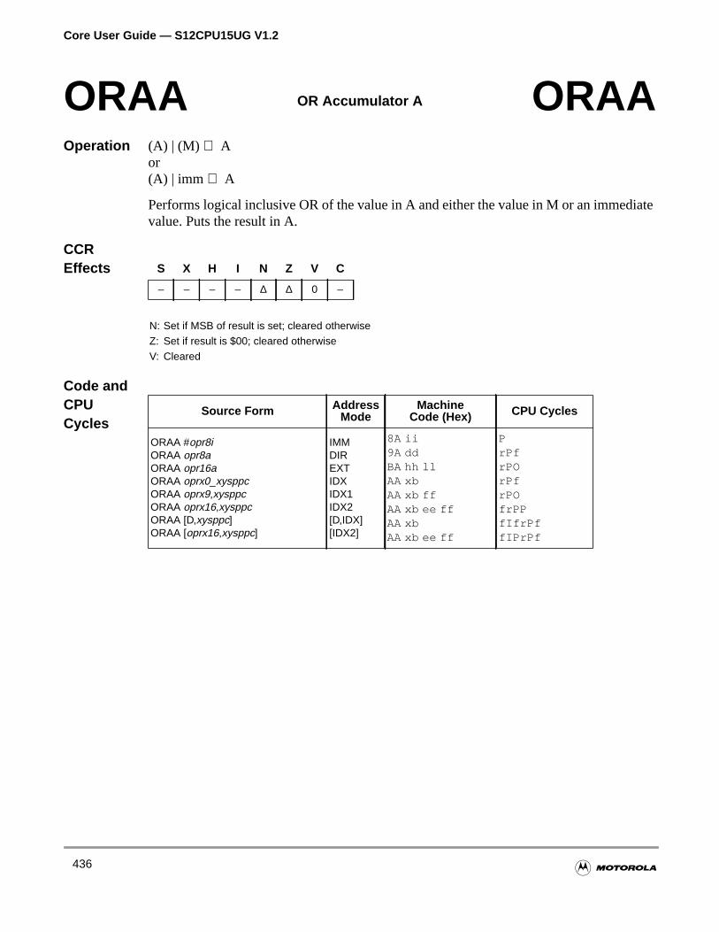
Core User Guide — S12CPU15UG V1.2
ate
Operation (A) | (M) ⇒ Aor(A) | imm ⇒ A
Performs logical inclusive OR of the value in A and either the value in M or an immedivalue. Puts the result in A.
CCREffects
Code andCPUCycles
ORAA OR Accumulator A ORAA
S X H I N Z V C
– – – – ∆ ∆ 0 –
N: Set if MSB of result is set; cleared otherwiseZ: Set if result is $00; cleared otherwiseV: Cleared
Source Form AddressMode
MachineCode (Hex) CPU Cycles
ORAA #opr8iORAA opr8aORAA opr16aORAA oprx0_xysppcORAA oprx9,xysppcORAA oprx16,xysppcORAA [D,xysppc]ORAA [oprx16,xysppc]
IMMDIREXTIDXIDX1IDX2[D,IDX][IDX2]
8A ii9A ddBA hh llAA xbAA xb ffAA xb ee ffAA xbAA xb ee ff
PrPfrPOrPfrPOfrPPfIfrPffIPrPf
436

Core User Guide — S12CPU15UG V1.2
iate
Operation (B) | (M) ⇒ Bor(B) | imm⇒ B
Performs logical inclusive OR of the value in B and either the value in M or an immedvalue. Puts the result in B.
CCREffects
Code andCPUCycles
ORAB OR Accumulator B ORAB
S X H I N Z V C
– – – – ∆ ∆ 0 –
N: Set if MSB of result is set; cleared otherwiseZ: Set if result is $00; cleared otherwiseV: Cleared
Source Form AddressMode
Machine Coding(Hex) CPU Cycles
ORAB #opr8iORAB opr8aORAB opr16aORAB oprx0_xysppcORAB oprx9,xysppcORAB oprx16,xysppcORAB [D,xysppc]ORAB [oprx16,xysppc]
IMMDIREXTIDXIDX1IDX2[D,IDX][IDX2]
CA iiDA ddFA hh llEA xbEA xb ffEA xb ee ffEA xbEA xb ee ff
PrPfrPOrPfrPOfrPPfIfrPffIPrPf
437
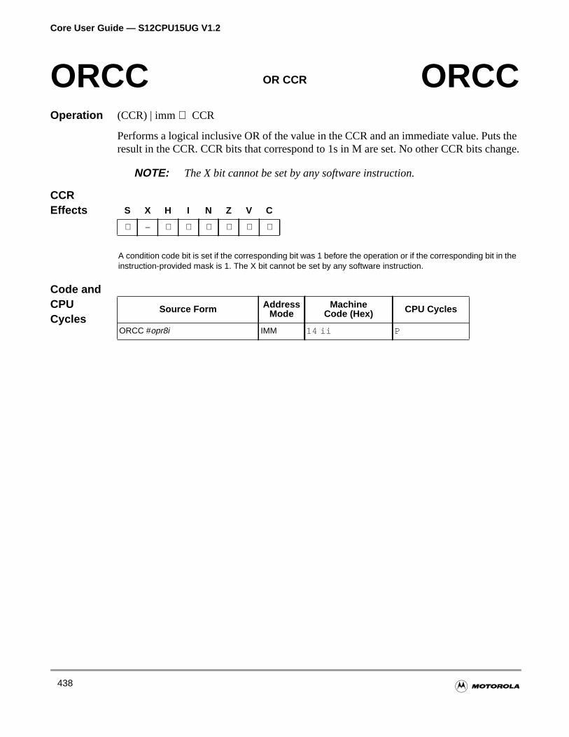
Core User Guide — S12CPU15UG V1.2
s theange.
Operation (CCR) | imm⇒ CCR
Performs a logical inclusive OR of the value in the CCR and an immediate value. Putresult in the CCR. CCR bits that correspond to 1s in M are set. No other CCR bits ch
NOTE: The X bit cannot be set by any software instruction.
CCREffects
Code andCPUCycles
ORCC OR CCR ORCC
S X H I N Z V C
⇑ – ⇑ ⇑ ⇑ ⇑ ⇑ ⇑
A condition code bit is set if the corresponding bit was 1 before the operation or if the corresponding bit in theinstruction-provided mask is 1. The X bit cannot be set by any software instruction.
Source Form AddressMode
MachineCode (Hex) CPU Cycles
ORCC #opr8i IMM 14 ii P
438
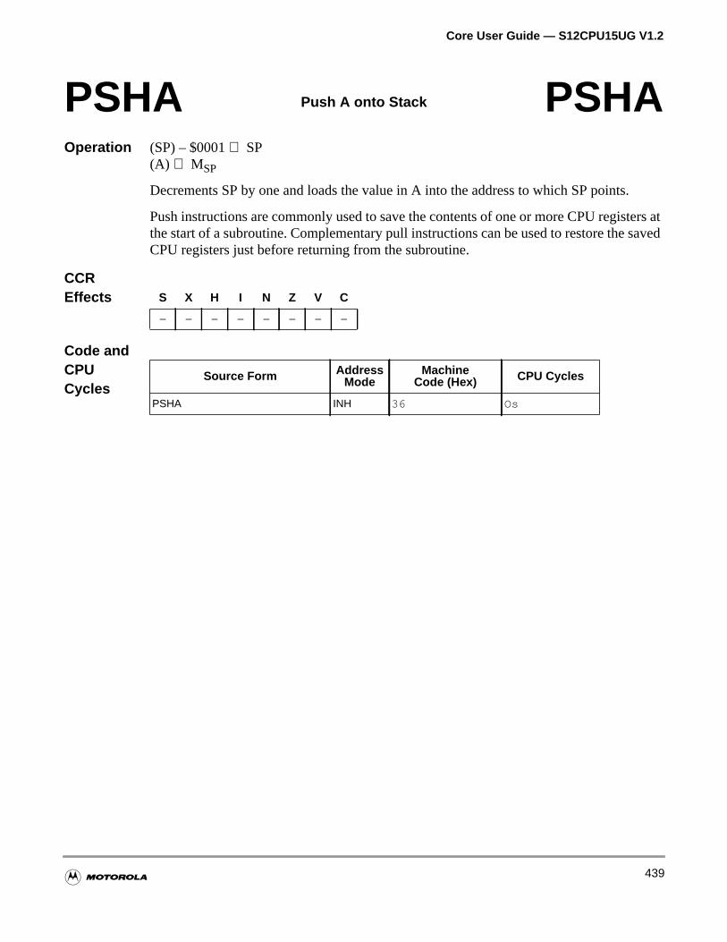
Core User Guide — S12CPU15UG V1.2
.
ters atsaved
Operation (SP) – $0001⇒ SP(A) ⇒ MSP
Decrements SP by one and loads the value in A into the address to which SP points
Push instructions are commonly used to save the contents of one or more CPU registhe start of a subroutine. Complementary pull instructions can be used to restore theCPU registers just before returning from the subroutine.
CCREffects
Code andCPUCycles
PSHA Push A onto Stack PSHA
S X H I N Z V C
– – – – – – – –
Source Form AddressMode
MachineCode (Hex) CPU Cycles
PSHA INH 36 Os
439
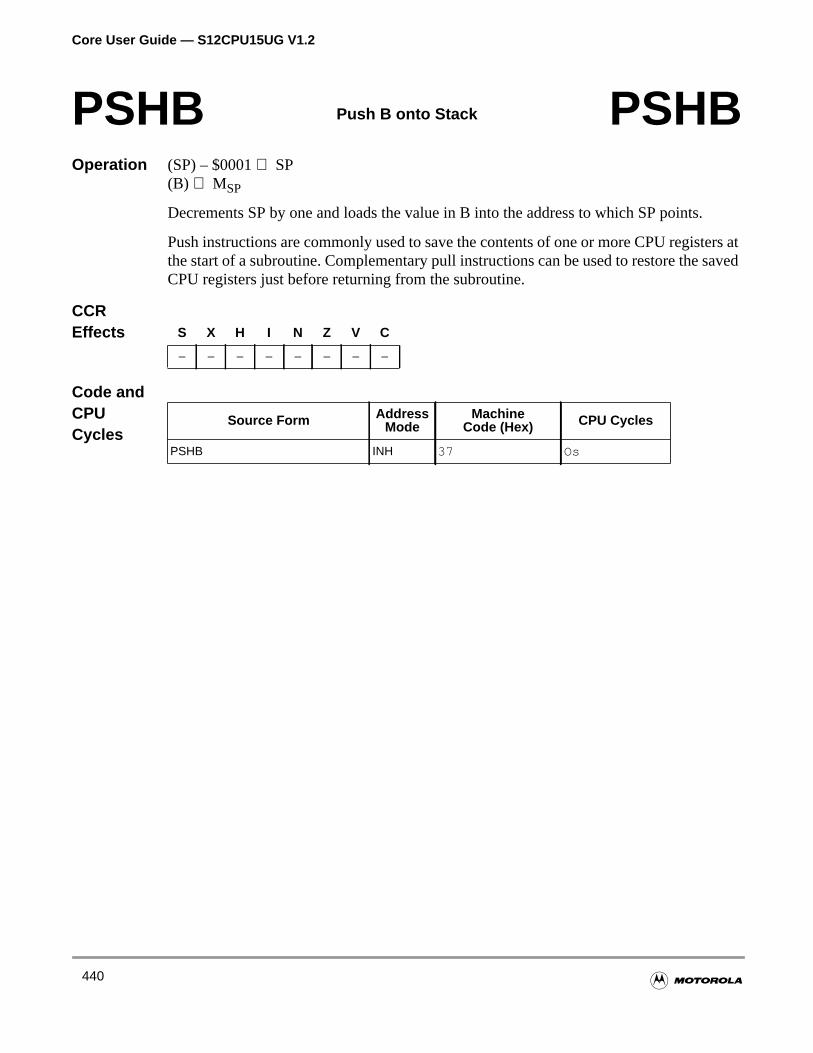
Core User Guide — S12CPU15UG V1.2
.
ters atsaved
Operation (SP) – $0001⇒ SP(B) ⇒ MSP
Decrements SP by one and loads the value in B into the address to which SP points
Push instructions are commonly used to save the contents of one or more CPU registhe start of a subroutine. Complementary pull instructions can be used to restore theCPU registers just before returning from the subroutine.
CCREffects
Code andCPUCycles
PSHB Push B onto Stack PSHB
S X H I N Z V C
– – – – – – – –
Source Form AddressMode
MachineCode (Hex) CPU Cycles
PSHB INH 37 Os
440
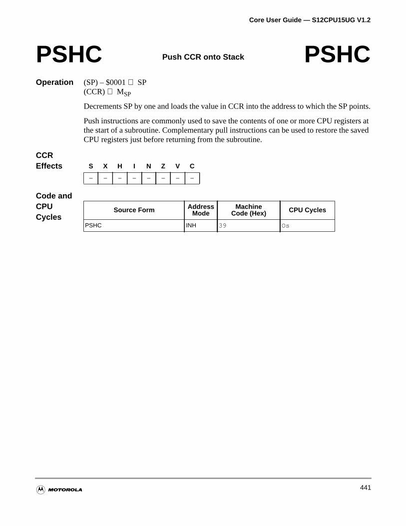
Core User Guide — S12CPU15UG V1.2
points.
ters atsaved
Operation (SP) – $0001⇒ SP(CCR)⇒ MSP
Decrements SP by one and loads the value in CCR into the address to which the SP
Push instructions are commonly used to save the contents of one or more CPU registhe start of a subroutine. Complementary pull instructions can be used to restore theCPU registers just before returning from the subroutine.
CCREffects
Code andCPUCycles
PSHC Push CCR onto Stack PSHC
S X H I N Z V C
– – – – – – – –
Source Form AddressMode
MachineCode (Hex) CPU Cycles
PSHC INH 39 Os
441

Core User Guide — S12CPU15UG V1.2
oadsoints
ters atU
Operation (SP) – $0002⇒ SP(A):(B) ⇒ MSP:MSP + 1
Decrements SP by two and loads the value in A into the address to which SP points. Lthe value in B into the address to which SP points plus one. After PSHD executes, SP pto the stacked value of A.
Push instructions are commonly used to save the contents of one or more CPU registhe start of a subroutine. Complementary pull instructions can restore the saved CPregisters just before returning from the subroutine.
CCREffects
Code andCPUCycles
PSHD Push D onto Stack PSHD
S X H I N Z V C
– – – – – – – –
Source Form AddressMode
MachineCode (Hex) CPU Cycles
PSHD INH 3B OS
442

Core User Guide — S12CPU15UG V1.2
ints.utes,
ters atU
Operation (SP) – $0002⇒ SP(XH):(XL) ⇒ MSP:MSP + 1
Decrements SP by two and loads the high byte of X into the address to which SP poLoads the low byte of X into the address to which SP points plus one. After PSHX execSP points to the stacked value of the high byte of X.
Push instructions are commonly used to save the contents of one or more CPU registhe start of a subroutine. Complementary pull instructions can restore the saved CPregisters just before returning from the subroutine.
CCREffects
Code andCPUCycles
PSHX Push X onto Stack PSHX
S X H I N Z V C
– – – – – – – –
Source Form AddressMode
MachineCode (Hex) CPU Cycles
PSHX INH 34 OS
443
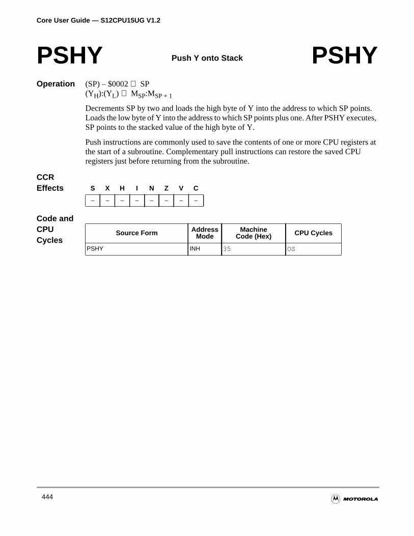
Core User Guide — S12CPU15UG V1.2
ints.utes,
ters atU
Operation (SP) – $0002⇒ SP(YH):(YL) ⇒ MSP:MSP + 1
Decrements SP by two and loads the high byte of Y into the address to which SP poLoads the low byte of Y into the address to which SP points plus one. After PSHY execSP points to the stacked value of the high byte of Y.
Push instructions are commonly used to save the contents of one or more CPU registhe start of a subroutine. Complementary pull instructions can restore the saved CPregisters just before returning from the subroutine.
CCREffects
Code andCPUCycles
PSHY Push Y onto Stack PSHY
S X H I N Z V C
– – – – – – – –
Source Form AddressMode
MachineCode (Hex) CPU Cycles
PSHY INH 35 OS
444
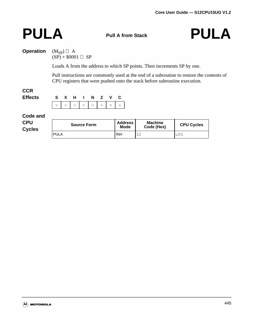
Core User Guide — S12CPU15UG V1.2
ts of
Operation (MSP) ⇒ A(SP) + $0001⇒ SP
Loads A from the address to which SP points. Then increments SP by one.
Pull instructions are commonly used at the end of a subroutine to restore the contenCPU registers that were pushed onto the stack before subroutine execution.
CCREffects
Code andCPUCycles
PULA Pull A from Stack PULA
S X H I N Z V C
– – – – – – – –
Source Form AddressMode
MachineCode (Hex) CPU Cycles
PULA INH 32 ufO
445
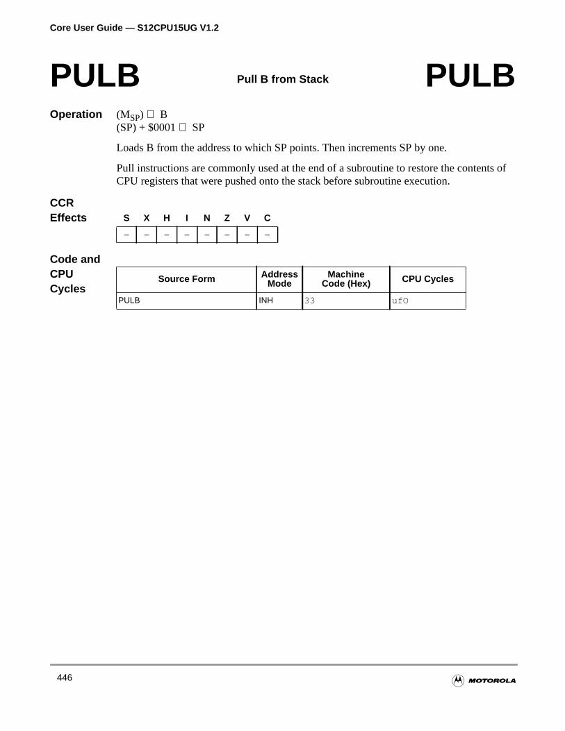
Core User Guide — S12CPU15UG V1.2
ts of
Operation (MSP) ⇒ B(SP) + $0001⇒ SP
Loads B from the address to which SP points. Then increments SP by one.
Pull instructions are commonly used at the end of a subroutine to restore the contenCPU registers that were pushed onto the stack before subroutine execution.
CCREffects
Code andCPUCycles
PULB Pull B from Stack PULB
S X H I N Z V C
– – – – – – – –
Source Form AddressMode
MachineCode (Hex) CPU Cycles
PULB INH 33 ufO
446
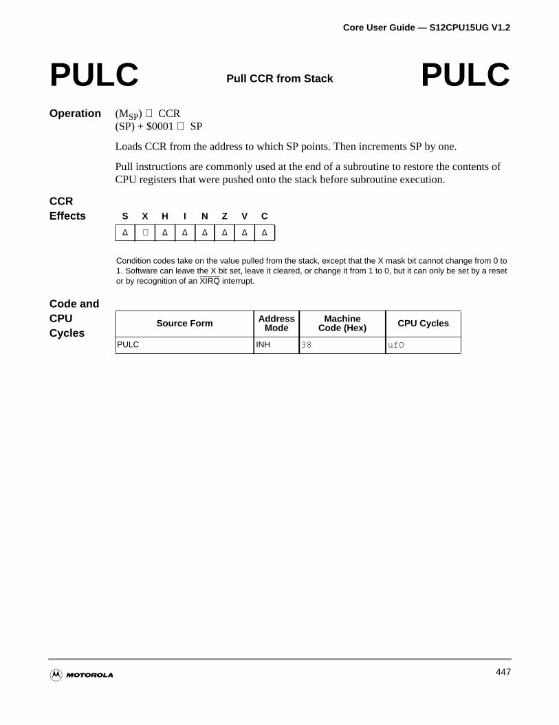
Core User Guide — S12CPU15UG V1.2
ts of
Operation (MSP) ⇒ CCR(SP) + $0001⇒ SP
Loads CCR from the address to which SP points. Then increments SP by one.
Pull instructions are commonly used at the end of a subroutine to restore the contenCPU registers that were pushed onto the stack before subroutine execution.
CCREffects
Code andCPUCycles
PULC Pull CCR from Stack PULC
S X H I N Z V C
∆ ⇓ ∆ ∆ ∆ ∆ ∆ ∆
Condition codes take on the value pulled from the stack, except that the X mask bit cannot change from 0 to1. Software can leave the X bit set, leave it cleared, or change it from 1 to 0, but it can only be set by a resetor by recognition of an XIRQ interrupt.
Source Form AddressMode
MachineCode (Hex) CPU Cycles
PULC INH 38 ufO
447
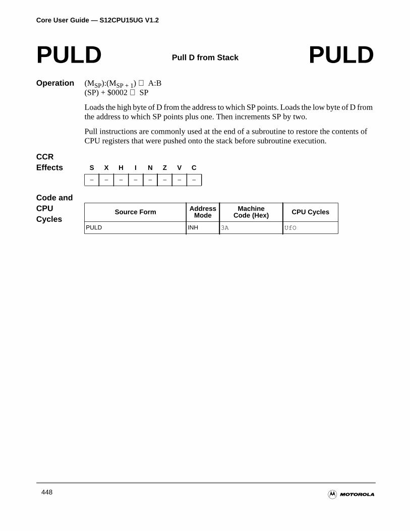
Core User Guide — S12CPU15UG V1.2
rom
ts of
Operation (MSP):(MSP + 1) ⇒ A:B(SP) + $0002⇒ SP
Loads the high byte of D from the address to which SP points. Loads the low byte of D fthe address to which SP points plus one. Then increments SP by two.
Pull instructions are commonly used at the end of a subroutine to restore the contenCPU registers that were pushed onto the stack before subroutine execution.
CCREffects
Code andCPUCycles
PULD Pull D from Stack PULD
S X H I N Z V C
– – – – – – – –
Source Form AddressMode
MachineCode (Hex) CPU Cycles
PULD INH 3A UfO
448
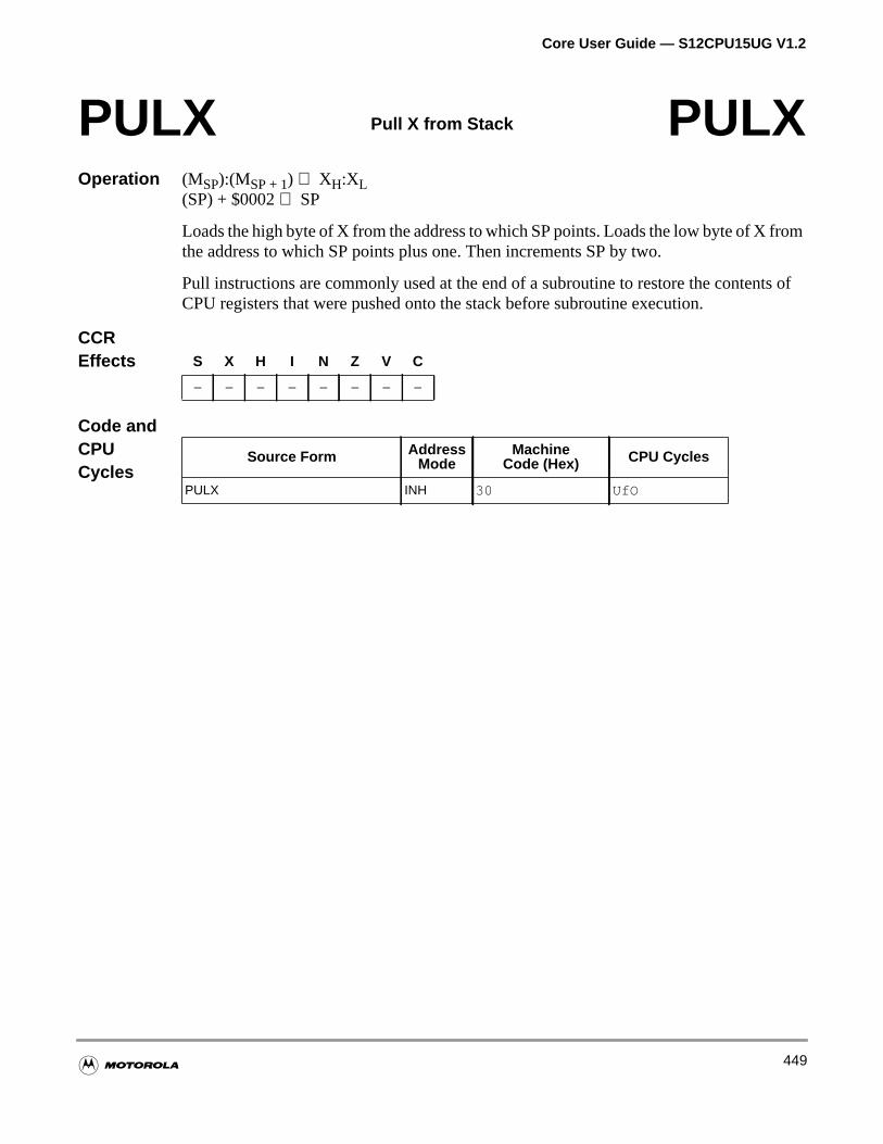
Core User Guide — S12CPU15UG V1.2
rom
ts of
Operation (MSP):(MSP + 1) ⇒ XH:XL(SP) + $0002⇒ SP
Loads the high byte of X from the address to which SP points. Loads the low byte of X fthe address to which SP points plus one. Then increments SP by two.
Pull instructions are commonly used at the end of a subroutine to restore the contenCPU registers that were pushed onto the stack before subroutine execution.
CCREffects
Code andCPUCycles
PULX Pull X from Stack PULX
S X H I N Z V C
– – – – – – – –
Source Form AddressMode
MachineCode (Hex) CPU Cycles
PULX INH 30 UfO
449
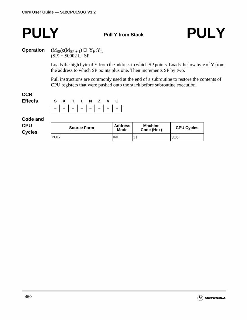
Core User Guide — S12CPU15UG V1.2
rom
ts of
Operation (MSP):(MSP + 1) ⇒ YH:YL(SP) + $0002⇒ SP
Loads the high byte of Y from the address to which SP points. Loads the low byte of Y fthe address to which SP points plus one. Then increments SP by two.
Pull instructions are commonly used at the end of a subroutine to restore the contenCPU registers that were pushed onto the stack before subroutine execution.
CCREffects
Code andCPUCycles
PULY Pull Y from Stack PULY
S X H I N Z V C
– – – – – – – –
Source Form AddressMode
MachineCode (Hex) CPU Cycles
PULY INH 31 UfO
450
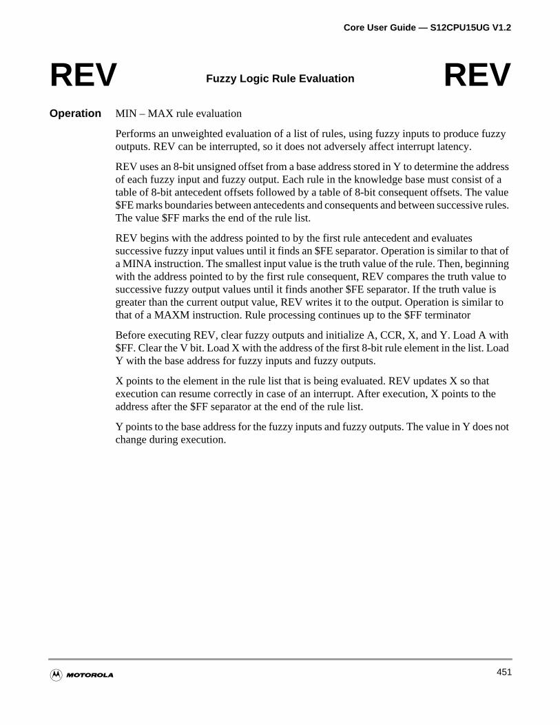
Core User Guide — S12CPU15UG V1.2
zzy
dress of aalue
ive rules.
at ofinglue to isr to
ithad
the
s not
Operation MIN – MAX rule evaluation
Performs an unweighted evaluation of a list of rules, using fuzzy inputs to produce fuoutputs. REV can be interrupted, so it does not adversely affect interrupt latency.
REV uses an 8-bit unsigned offset from a base address stored in Y to determine the adof each fuzzy input and fuzzy output. Each rule in the knowledge base must consisttable of 8-bit antecedent offsets followed by a table of 8-bit consequent offsets. The v$FE marks boundaries between antecedents and consequents and between successThe value $FF marks the end of the rule list.
REV begins with the address pointed to by the first rule antecedent and evaluatessuccessive fuzzy input values until it finds an $FE separator. Operation is similar to tha MINA instruction. The smallest input value is the truth value of the rule. Then, beginnwith the address pointed to by the first rule consequent, REV compares the truth vasuccessive fuzzy output values until it finds another $FE separator. If the truth valuegreater than the current output value, REV writes it to the output. Operation is similathat of a MAXM instruction. Rule processing continues up to the $FF terminator
Before executing REV, clear fuzzy outputs and initialize A, CCR, X, and Y. Load A w$FF. Clear the V bit. Load X with the address of the first 8-bit rule element in the list. LoY with the base address for fuzzy inputs and fuzzy outputs.
X points to the element in the rule list that is being evaluated. REV updates X so thaexecution can resume correctly in case of an interrupt. After execution, X points to taddress after the $FF separator at the end of the rule list.
Y points to the base address for the fuzzy inputs and fuzzy outputs. The value in Y doechange during execution.
REV Fuzzy Logic Rule Evaluation REV
451
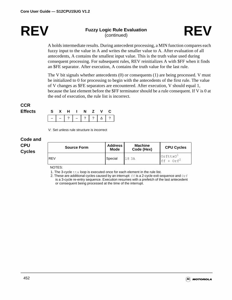
Core User Guide — S12CPU15UG V1.2
each
finds
mustalue,is 0 at
A holds intermediate results. During antecedent processing, a MIN function comparesfuzzy input to the value in A and writes the smaller value to A. After evaluation of allantecedents, A contains the smallest input value. This is the truth value used duringconsequent processing. For subsequent rules, REV reinitializes A with $FF when it an $FE separator. After execution, A contains the truth value for the last rule.
The V bit signals whether antecedents (0) or consequents (1) are being processed. Vbe initialized to 0 for processing to begin with the antecedents of the first rule. The vof V changes as $FE separators are encountered. After execution, V should equal 1because the last element before the $FF terminator should be a rule consequent. If Vthe end of execution, the rule list is incorrect.
CCREffects
Code andCPUCycles
REV Fuzzy Logic Rule Evaluation(continued) REV
S X H I N Z V C
– – ? – ? ? ∆ ?
V: Set unless rule structure is incorrect
Source Form AddressMode
MachineCode (Hex) CPU Cycles
REV Special 18 3AOrfttxO 1
ff + Orf 2
NOTES:1. The 3-cycle ttx loop is executed once for each element in the rule list.2. These are additional cycles caused by an interrupt: ff is a 2-cycle exit sequence and Orf
is a 3-cycle re-entry sequence. Execution resumes with a prefetch of the last antecedentor consequent being processed at the time of the interrupt.
452
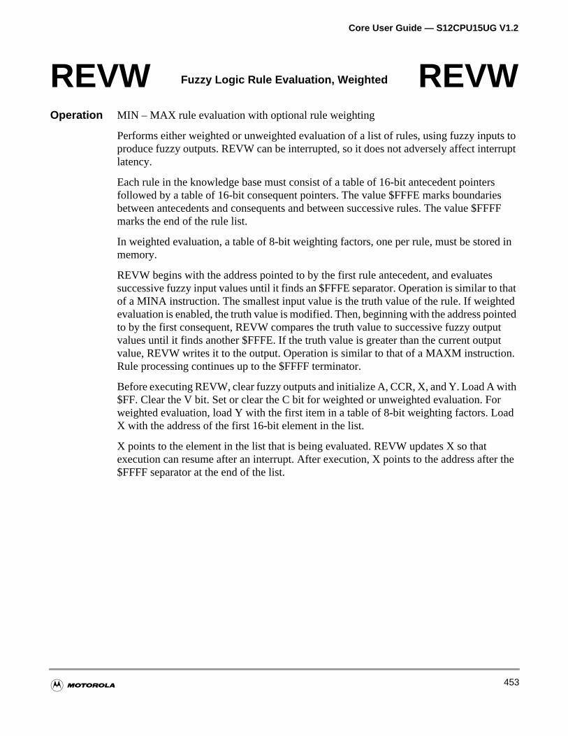
Core User Guide — S12CPU15UG V1.2
s torrupt
rsesFFFF
d in
sthattedintedututn.
ithrad
er the
Operation MIN – MAX rule evaluation with optional rule weighting
Performs either weighted or unweighted evaluation of a list of rules, using fuzzy inputproduce fuzzy outputs. REVW can be interrupted, so it does not adversely affect intelatency.
Each rule in the knowledge base must consist of a table of 16-bit antecedent pointefollowed by a table of 16-bit consequent pointers. The value $FFFE marks boundaribetween antecedents and consequents and between successive rules. The value $marks the end of the rule list.
In weighted evaluation, a table of 8-bit weighting factors, one per rule, must be storememory.
REVW begins with the address pointed to by the first rule antecedent, and evaluatesuccessive fuzzy input values until it finds an $FFFE separator. Operation is similar toof a MINA instruction. The smallest input value is the truth value of the rule. If weighevaluation is enabled, the truth value is modified. Then, beginning with the address poto by the first consequent, REVW compares the truth value to successive fuzzy outpvalues until it finds another $FFFE. If the truth value is greater than the current outpvalue, REVW writes it to the output. Operation is similar to that of a MAXM instructioRule processing continues up to the $FFFF terminator.
Before executing REVW, clear fuzzy outputs and initialize A, CCR, X, and Y. Load A w$FF. Clear the V bit. Set or clear the C bit for weighted or unweighted evaluation. Foweighted evaluation, load Y with the first item in a table of 8-bit weighting factors. LoX with the address of the first 16-bit element in the list.
X points to the element in the list that is being evaluated. REVW updates X so thatexecution can resume after an interrupt. After execution, X points to the address aft$FFFF separator at the end of the list.
REVW Fuzzy Logic Rule Evaluation, Weighted REVW
453
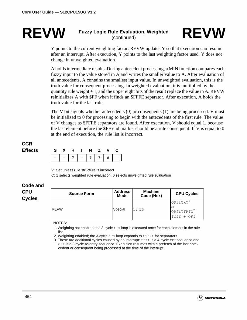
Core User Guide — S12CPU15UG V1.2
umenot
eachn ofs the
VWe
mustaluecausel to 0
Y points to the current weighting factor. REVW updates Y so that execution can resafter an interrupt. After execution, Y points to the last weighting factor used. Y does change in unweighted evaluation.
A holds intermediate results. During antecedent processing, a MIN function comparesfuzzy input to the value stored in A and writes the smaller value to A. After evaluatioall antecedents, A contains the smallest input value. In unweighted evaluation, this itruth value for consequent processing. In weighted evaluation, it is multiplied by thequantity rule weight + 1, and the upper eight bits of the result replace the value in A. REreinitializes A with $FF when it finds an $FFFE separator. After execution, A holds thtruth value for the last rule.
The V bit signals whether antecedents (0) or consequents (1) are being processed. Vbe initialized to 0 for processing to begin with the antecedents of the first rule. The vof V changes as $FFFE separators are found. After execution, V should equal 1, bethe last element before the $FF end marker should be a rule consequent. If V is equaat the end of execution, the rule list is incorrect.
CCREffects
Code andCPUCycles
REVW Fuzzy Logic Rule Evaluation, Weighted(continued) REVW
S X H I N Z V C
– – ? – ? ? ∆ !
V: Set unless rule structure is incorrectC: 1 selects weighted rule evaluation; 0 selects unweighted rule evaluation
Source Form AddressMode
MachineCode (Hex) CPU Cycles
REVW Special 18 3B
ORftTxO 1
orORftTfRfO 2
ffff + ORf 3
NOTES:1. Weighting not enabled; the 3-cycle tTx loop is executed once for each element in the rule
list.2. Weighting enabled; the 3-cycle tTx loop expands to tTfRf for separators.3. These are additional cycles caused by an interrupt: ffff is a 4-cycle exit sequence and
ORf is a 3-cycle re-entry sequence. Execution resumes with a prefetch of the last ante-cedent or consequent being processed at the time of the interrupt.
454

Core User Guide — S12CPU15UG V1.2
ed
bitede,
Operation
Shifts all bits of M one place to the left. Bit 0 is loaded from the C bit. The C bit is loadfrom the most significant bit of M. Rotate operations include the carry bit to allowextension of shift and rotate operations to multiple bytes. For example, to shift a 24-value one bit to the left, the sequence ASL LOW, ROL MID, ROL HIGH could be uswhere LOW, MID, and HIGH refer to the low, middle, and high bytes of the 24-bit valurespectively.
CCREffects
Code andCPUCycles
ROL Rotate Left M ROLb7 b6 b5 b4 b3 b2 b1 b0C
M
S X H I N Z V C
– – – – ∆ ∆ ∆ ∆
N: Set if MSB of result is set; cleared otherwiseZ: Set if result is $00; cleared otherwiseV: N ⊕ C = [N • C] | [N • C] (for N and C after the shift); set if (N is set and C is cleared) or (N is cleared and
C is set); cleared otherwise (for values of N and C after the shift)C: M7; set if the MSB of M was set before the shift; cleared otherwise
Source Form AddressMode
MachineCode (Hex) CPU Cycles
ROL opr16aROL oprx0_xysppcROL oprx9,xysppcROL oprx16,xysppcROL [D,xysppc]ROL [oprx16,xysppc]
EXTIDXIDX1IDX2[D,IDX][IDX2]
75 hh ll65 xb65 xb ff65 xb ee ff65 xb65 xb ee ff
rPwOrPwrPwOfrPwPfIfrPwfIPrPw
455
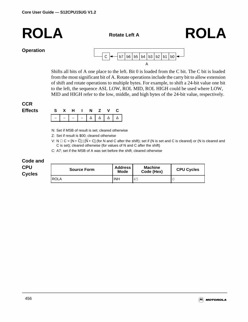
Core User Guide — S12CPU15UG V1.2
edion
e bit,
ely.
Operation
Shifts all bits of A one place to the left. Bit 0 is loaded from the C bit. The C bit is loadfrom the most significant bit of A. Rotate operations include the carry bit to allow extensof shift and rotate operations to multiple bytes. For example, to shift a 24-bit value onto the left, the sequence ASL LOW, ROL MID, ROL HIGH could be used where LOWMID and HIGH refer to the low, middle, and high bytes of the 24-bit value, respectiv
CCREffects
Code andCPUCycles
ROLA Rotate Left A ROLAb7 b6 b5 b4 b3 b2 b1 b0C
A
S X H I N Z V C
– – – – ∆ ∆ ∆ ∆
N: Set if MSB of result is set; cleared otherwiseZ: Set if result is $00; cleared otherwiseV: N ⊕ C = [N • C] | [N • C] (for N and C after the shift); set if (N is set and C is cleared) or (N is cleared and
C is set); cleared otherwise (for values of N and C after the shift)C: A7; set if the MSB of A was set before the shift; cleared otherwise
Source Form AddressMode
MachineCode (Hex) CPU Cycles
ROLA INH 45 O
456
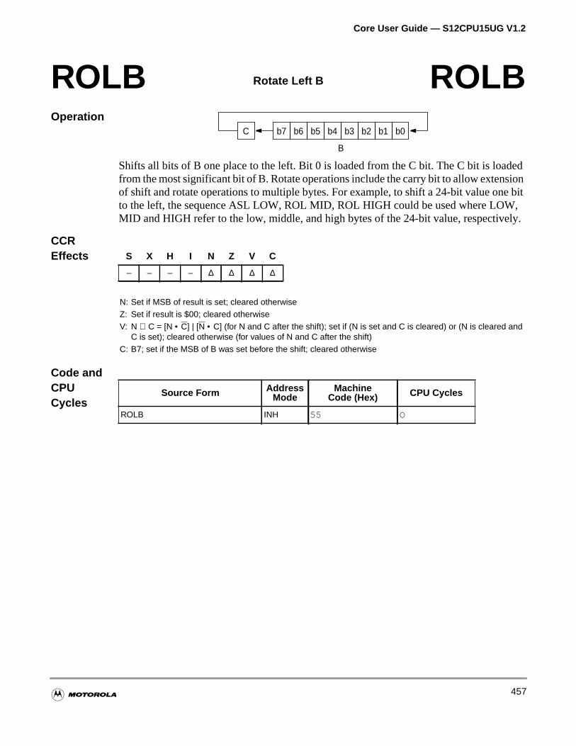
Core User Guide — S12CPU15UG V1.2
dedion
e bit,
ely.
Operation
Shifts all bits of B one place to the left. Bit 0 is loaded from the C bit. The C bit is loafrom the most significant bit of B. Rotate operations include the carry bit to allow extensof shift and rotate operations to multiple bytes. For example, to shift a 24-bit value onto the left, the sequence ASL LOW, ROL MID, ROL HIGH could be used where LOWMID and HIGH refer to the low, middle, and high bytes of the 24-bit value, respectiv
CCREffects
Code andCPUCycles
ROLB Rotate Left B ROLBb7 b6 b5 b4 b3 b2 b1 b0C
B
S X H I N Z V C
– – – – ∆ ∆ ∆ ∆
N: Set if MSB of result is set; cleared otherwiseZ: Set if result is $00; cleared otherwiseV: N ⊕ C = [N • C] | [N • C] (for N and C after the shift); set if (N is set and C is cleared) or (N is cleared and
C is set); cleared otherwise (for values of N and C after the shift)C: B7; set if the MSB of B was set before the shift; cleared otherwise
Source Form AddressMode
MachineCode (Hex) CPU Cycles
ROLB INH 55 O
457
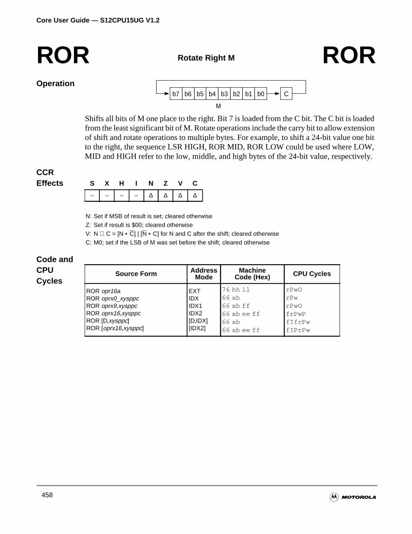
Core User Guide — S12CPU15UG V1.2
edion
e bitW,ely.
Operation
Shifts all bits of M one place to the right. Bit 7 is loaded from the C bit. The C bit is loadfrom the least significant bit of M. Rotate operations include the carry bit to allow extensof shift and rotate operations to multiple bytes. For example, to shift a 24-bit value onto the right, the sequence LSR HIGH, ROR MID, ROR LOW could be used where LOMID and HIGH refer to the low, middle, and high bytes of the 24-bit value, respectiv
CCREffects
Code andCPUCycles
ROR Rotate Right M RORb7 b6 b5 b4 b3 b2 b1 b0 C
M
S X H I N Z V C
– – – – ∆ ∆ ∆ ∆
N: Set if MSB of result is set; cleared otherwiseZ: Set if result is $00; cleared otherwiseV: N ⊕ C = [N • C] | [N • C] for N and C after the shift; cleared otherwiseC: M0; set if the LSB of M was set before the shift; cleared otherwise
Source Form AddressMode
MachineCode (Hex) CPU Cycles
ROR opr16aROR oprx0_xysppcROR oprx9,xysppcROR oprx16,xysppcROR [D,xysppc]ROR [oprx16,xysppc]
EXTIDXIDX1IDX2[D,IDX][IDX2]
76 hh ll66 xb66 xb ff66 xb ee ff66 xb66 xb ee ff
rPwOrPwrPwOfrPwPfIfrPwfIPrPw
458
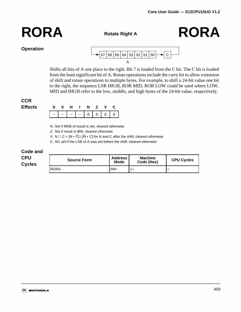
Core User Guide — S12CPU15UG V1.2
edion
e bitW,ely.
Operation
Shifts all bits of A one place to the right. Bit 7 is loaded from the C bit. The C bit is loadfrom the least significant bit of A. Rotate operations include the carry bit to allow extensof shift and rotate operations to multiple bytes. For example, to shift a 24-bit value onto the right, the sequence LSR HIGH, ROR MID, ROR LOW could be used where LOMID and HIGH refer to the low, middle, and high bytes of the 24-bit value, respectiv
CCREffects
Code andCPUCycles
RORA Rotate Right A RORAb7 b6 b5 b4 b3 b2 b1 b0 C
A
S X H I N Z V C
– – – – ∆ ∆ ∆ ∆
N: Set if MSB of result is set; cleared otherwiseZ: Set if result is $00; cleared otherwiseV: N ⊕ C = [N • C] | [N • C] for N and C after the shift; cleared otherwiseC: A0; set if the LSB of A was set before the shift; cleared otherwise
Source Form AddressMode
MachineCode (Hex) CPU Cycles
RORA INH 46 O
459
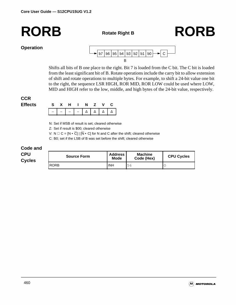
Core User Guide — S12CPU15UG V1.2
edion
e bitW,ely.
Operation
Shifts all bits of B one place to the right. Bit 7 is loaded from the C bit. The C bit is loadfrom the least significant bit of B. Rotate operations include the carry bit to allow extensof shift and rotate operations to multiple bytes. For example, to shift a 24-bit value onto the right, the sequence LSR HIGH, ROR MID, ROR LOW could be used where LOMID and HIGH refer to the low, middle, and high bytes of the 24-bit value, respectiv
CCREffects
Code andCPUCycles
RORB Rotate Right B RORBb7 b6 b5 b4 b3 b2 b1 b0 C
B
S X H I N Z V C
– – – – ∆ ∆ ∆ ∆
N: Set if MSB of result is set; cleared otherwiseZ: Set if result is $00; cleared otherwiseV: N ⊕ C = [N • C] | [N • C] for N and C after the shift; cleared otherwiseC: B0; set if the LSB of B was set before the shift; cleared otherwise
Source Form AddressMode
MachineCode (Hex) CPU Cycles
RORB INH 56 O
460
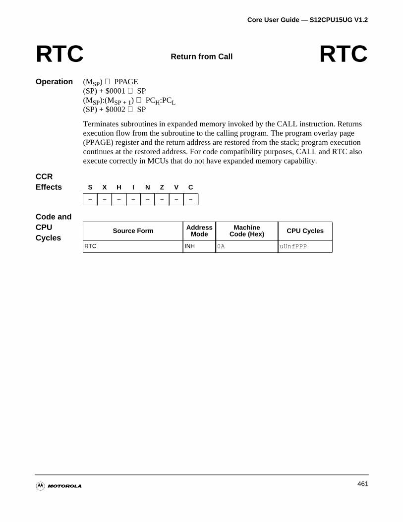
Core User Guide — S12CPU15UG V1.2
rnseution also
Operation (MSP) ⇒ PPAGE(SP) + $0001⇒ SP(MSP):(MSP + 1) ⇒ PCH:PCL(SP) + $0002⇒ SP
Terminates subroutines in expanded memory invoked by the CALL instruction. Retuexecution flow from the subroutine to the calling program. The program overlay pag(PPAGE) register and the return address are restored from the stack; program execcontinues at the restored address. For code compatibility purposes, CALL and RTCexecute correctly in MCUs that do not have expanded memory capability.
CCREffects
Code andCPUCycles
RTC Return from Call RTC
S X H I N Z V C
– – – – – – – –
Source Form AddressMode
MachineCode (Hex) CPU Cycles
RTC INH 0A uUnfPPP
461
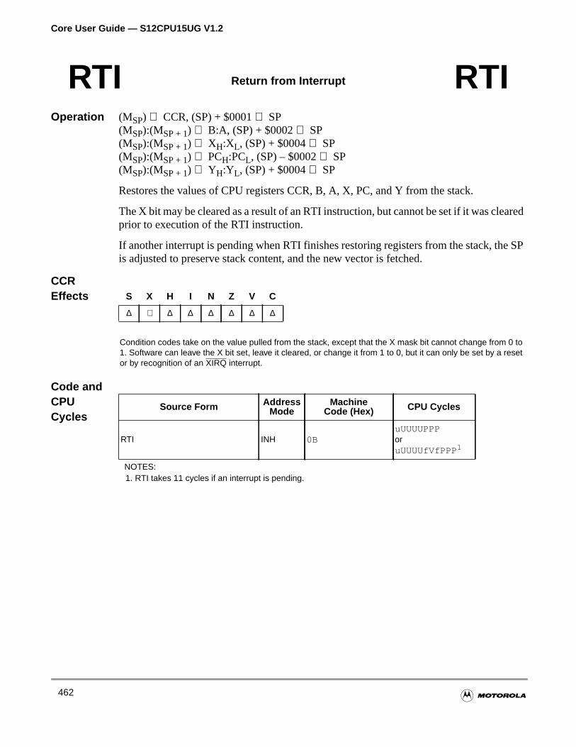
Core User Guide — S12CPU15UG V1.2
ared
e SP
Operation (MSP) ⇒ CCR, (SP) + $0001⇒ SP(MSP):(MSP + 1) ⇒ B:A, (SP) + $0002⇒ SP(MSP):(MSP + 1) ⇒ XH:XL, (SP) + $0004⇒ SP(MSP):(MSP + 1) ⇒ PCH:PCL, (SP) – $0002⇒ SP(MSP):(MSP + 1) ⇒ YH:YL, (SP) + $0004⇒ SP
Restores the values of CPU registers CCR, B, A, X, PC, and Y from the stack.
The X bit may be cleared as a result of an RTI instruction, but cannot be set if it was cleprior to execution of the RTI instruction.
If another interrupt is pending when RTI finishes restoring registers from the stack, this adjusted to preserve stack content, and the new vector is fetched.
CCREffects
Code andCPUCycles
RTI Return from Interrupt RTI
S X H I N Z V C
∆ ⇓ ∆ ∆ ∆ ∆ ∆ ∆
Condition codes take on the value pulled from the stack, except that the X mask bit cannot change from 0 to1. Software can leave the X bit set, leave it cleared, or change it from 1 to 0, but it can only be set by a resetor by recognition of an XIRQ interrupt.
Source Form AddressMode
MachineCode (Hex) CPU Cycles
RTI INH 0BuUUUUPPPoruUUUUfVfPPP1
NOTES:1. RTI takes 11 cycles if an interrupt is pending.
462
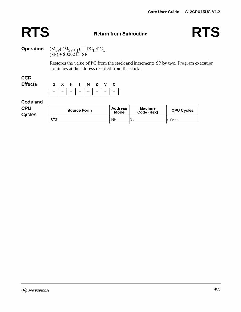
Core User Guide — S12CPU15UG V1.2
tion
Operation (MSP):(MSP + 1) ⇒ PCH:PCL(SP) + $0002⇒ SP
Restores the value of PC from the stack and increments SP by two. Program execucontinues at the address restored from the stack.
CCREffects
Code andCPUCycles
RTS Return from Subroutine RTS
S X H I N Z V C
– – – – – – – –
Source Form AddressMode
MachineCode (Hex) CPU Cycles
RTS INH 3D UfPPP
463
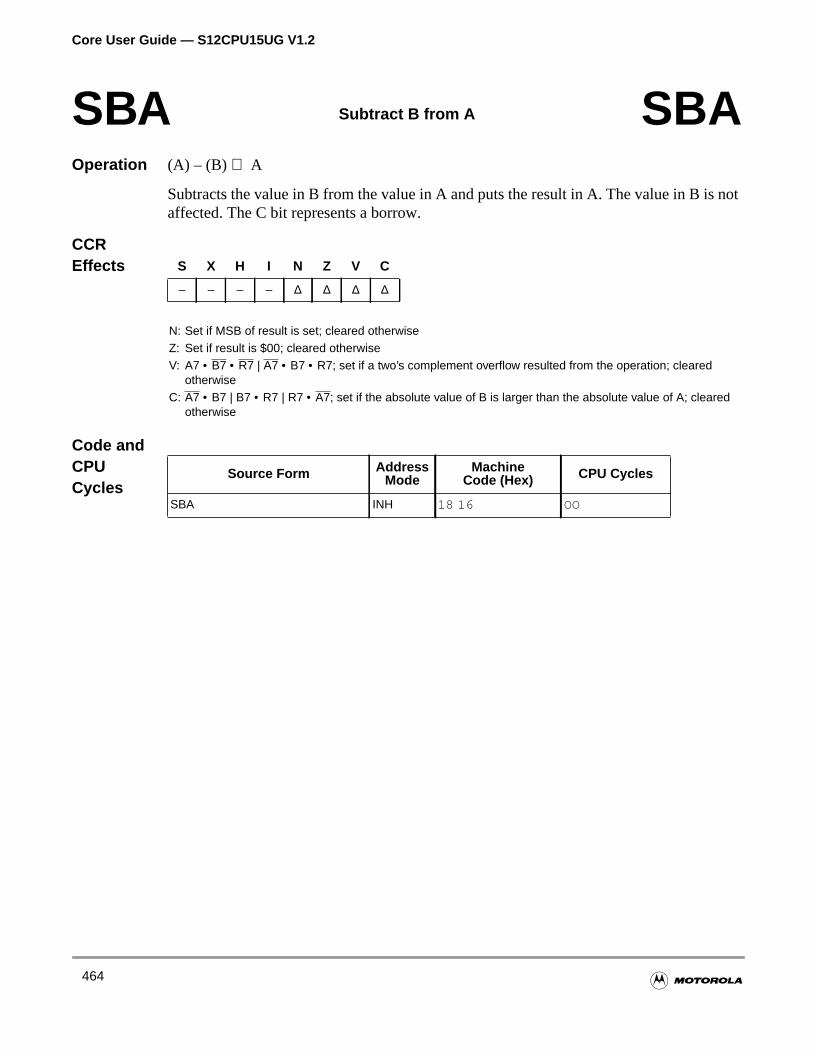
Core User Guide — S12CPU15UG V1.2
not
Operation (A) – (B) ⇒ A
Subtracts the value in B from the value in A and puts the result in A. The value in B isaffected. The C bit represents a borrow.
CCREffects
Code andCPUCycles
SBA Subtract B from A SBA
S X H I N Z V C
– – – – ∆ ∆ ∆ ∆
N: Set if MSB of result is set; cleared otherwiseZ: Set if result is $00; cleared otherwiseV: A7 • B7 • R7 | A7 • B7 • R7; set if a two’s complement overflow resulted from the operation; cleared
otherwiseC: A7 • B7 | B7 • R7 | R7 • A7; set if the absolute value of B is larger than the absolute value of A; cleared
otherwise
Source Form AddressMode
MachineCode (Hex) CPU Cycles
SBA INH 18 16 OO
464

Core User Guide — S12CPU15UG V1.2
the
Operation (A) – (M) – C⇒ Aor(A) – imm – C⇒ A
Subtracts either the value in M and the C bit or an immediate value and the C bit fromvalue in A. Puts the result in A. The C bit represents a borrow.
CCREffects
Code andCPUCycles
SBCA Subtract with Carry from A SBCA
S X H I N Z V C
– – – – ∆ ∆ ∆ ∆
N: Set if MSB of result is set; cleared otherwiseZ: Set if result is $00; cleared otherwiseV: A7 • M7 • R7 | A7 • M7 • R7; set if a two’s complement overflow resulted from the operation; cleared
otherwiseC: A7 • M7 | M7 • R7 | R7 • A7; set if the absolute value of the content of memory plus previous carry is
larger than the absolute value of A; cleared otherwise
Source Form AddressMode
MachineCode (Hex) CPU Cycles
SBCA #opr8iSBCA opr8aSBCA opr16aSBCA oprx0_xysppcSBCA oprx9,xysppcSBCA oprx16,xysppcSBCA [D,xysppc]SBCA [oprx16,xysppc]
IMMDIREXTIDXIDX1IDX2[D,IDX][IDX2]
82 ii92 ddB2 hh llA2 xbA2 xb ffA2 xb ee ffA2 xbA2 xb ee ff
PrPfrPOrPfrPOfrPPfIfrPffIPrPf
465
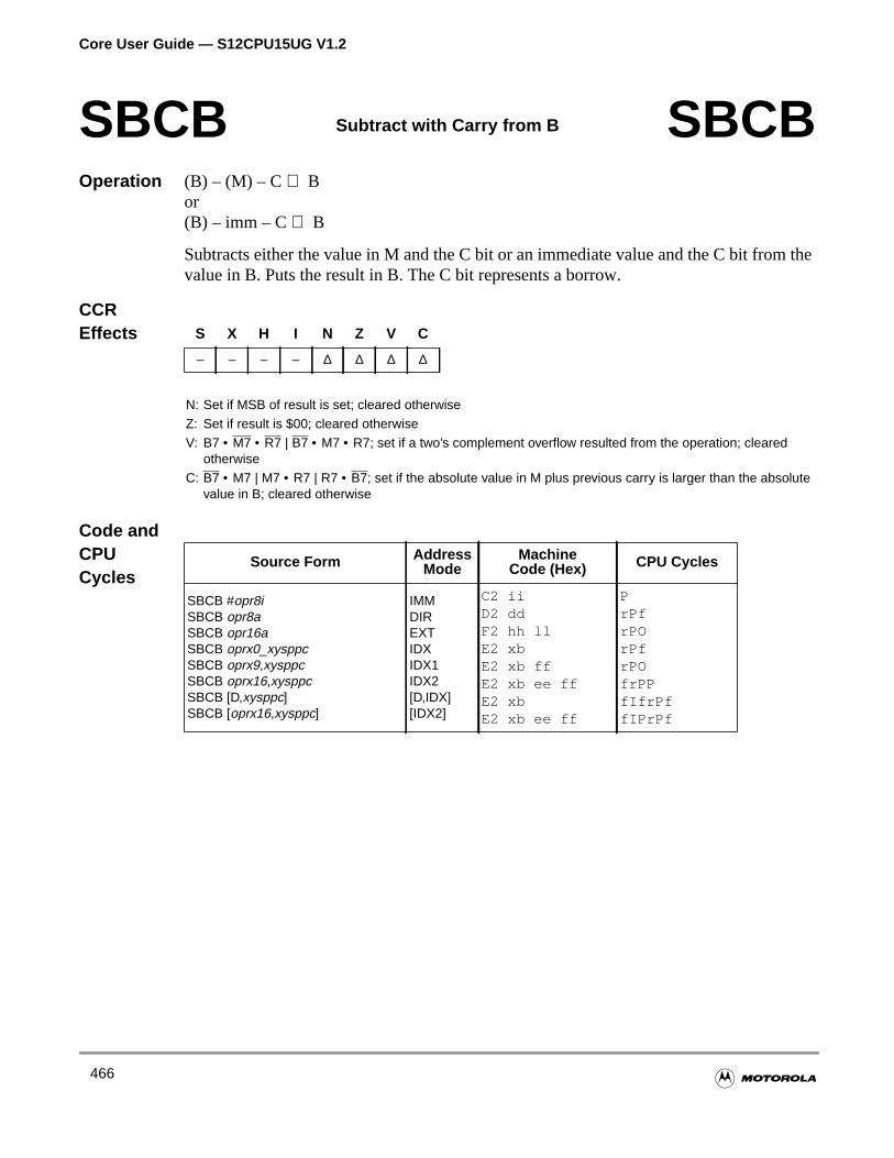
Core User Guide — S12CPU15UG V1.2
the
Operation (B) – (M) – C⇒ Bor(B) – imm – C⇒ B
Subtracts either the value in M and the C bit or an immediate value and the C bit fromvalue in B. Puts the result in B. The C bit represents a borrow.
CCREffects
Code andCPUCycles
SBCB Subtract with Carry from B SBCB
S X H I N Z V C
– – – – ∆ ∆ ∆ ∆
N: Set if MSB of result is set; cleared otherwiseZ: Set if result is $00; cleared otherwiseV: B7 • M7 • R7 | B7 • M7 • R7; set if a two’s complement overflow resulted from the operation; cleared
otherwiseC: B7 • M7 | M7 • R7 | R7 • B7; set if the absolute value in M plus previous carry is larger than the absolute
value in B; cleared otherwise
Source Form AddressMode
MachineCode (Hex) CPU Cycles
SBCB #opr8iSBCB opr8aSBCB opr16aSBCB oprx0_xysppcSBCB oprx9,xysppcSBCB oprx16,xysppcSBCB [D,xysppc]SBCB [oprx16,xysppc]
IMMDIREXTIDXIDX1IDX2[D,IDX][IDX2]
C2 iiD2 ddF2 hh llE2 xbE2 xb ffE2 xb ee ffE2 xbE2 xb ee ff
PrPfrPOrPfrPOfrPPfIfrPffIPrPf
466
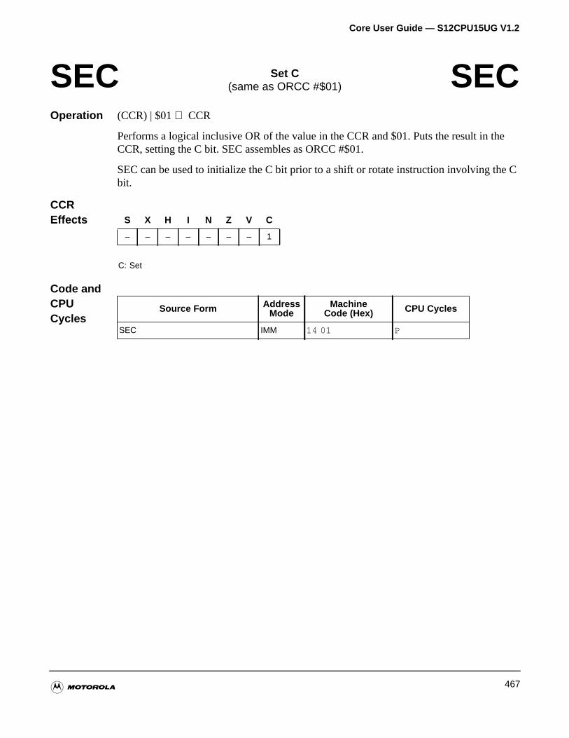
Core User Guide — S12CPU15UG V1.2
he
C
Operation (CCR) | $01⇒ CCR
Performs a logical inclusive OR of the value in the CCR and $01. Puts the result in tCCR, setting the C bit. SEC assembles as ORCC #$01.
SEC can be used to initialize the C bit prior to a shift or rotate instruction involving thebit.
CCREffects
Code andCPUCycles
SEC Set C(same as ORCC #$01) SEC
S X H I N Z V C
– – – – – – – 1
C: Set
Source Form AddressMode
MachineCode (Hex) CPU Cycles
SEC IMM 14 01 P
467
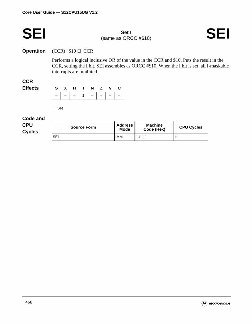
Core User Guide — S12CPU15UG V1.2
heable
Operation (CCR) | $10⇒ CCR
Performs a logical inclusive OR of the value in the CCR and $10. Puts the result in tCCR, setting the I bit. SEI assembles as ORCC #$10. When the I bit is set, all I-maskinterrupts are inhibited.
CCREffects
Code andCPUCycles
SEI Set I(same as ORCC #$10) SEI
S X H I N Z V C
– – – 1 – – – –
I: Set
Source Form AddressMode
MachineCode (Hex) CPU Cycles
SEI IMM 14 10 P
468
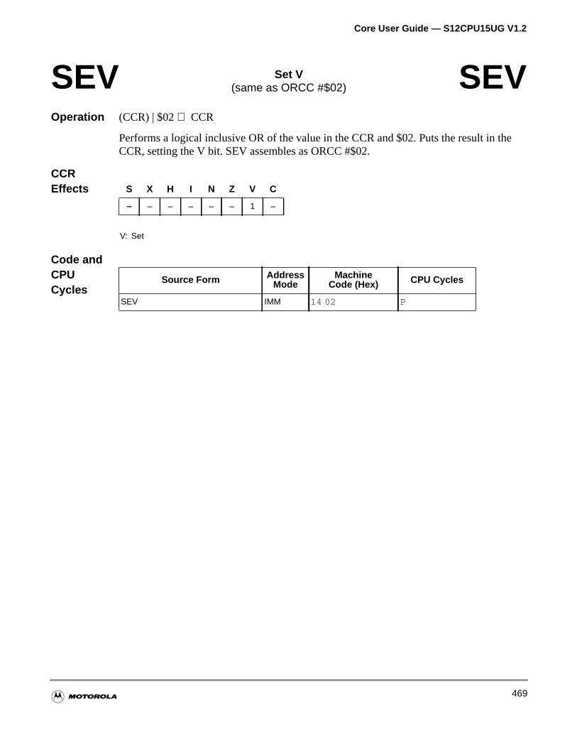
Core User Guide — S12CPU15UG V1.2
he
Operation (CCR) | $02⇒ CCR
Performs a logical inclusive OR of the value in the CCR and $02. Puts the result in tCCR, setting the V bit. SEV assembles as ORCC #$02.
CCREffects
Code andCPUCycles
SEV Set V(same as ORCC #$02) SEV
S X H I N Z V C
– – – – – – 1 –
V: Set
Source Form AddressMode
MachineCode (Hex) CPU Cycles
SEV IMM 14 02 P
469
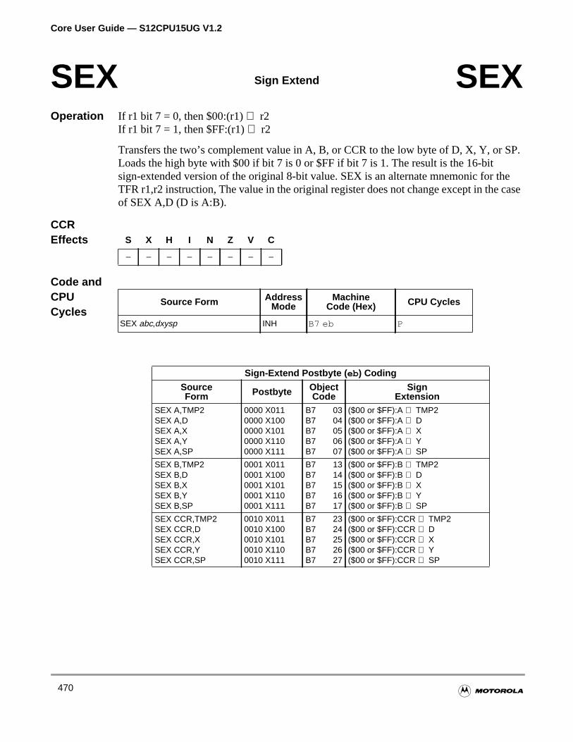
Core User Guide — S12CPU15UG V1.2
SP.
hecase
Operation If r1 bit 7 = 0, then $00:(r1)⇒ r2If r1 bit 7 = 1, then $FF:(r1)⇒ r2
Transfers the two’s complement value in A, B, or CCR to the low byte of D, X, Y, or Loads the high byte with $00 if bit 7 is 0 or $FF if bit 7 is 1. The result is the 16-bitsign-extended version of the original 8-bit value. SEX is an alternate mnemonic for tTFR r1,r2 instruction, The value in the original register does not change except in theof SEX A,D (D is A:B).
CCREffects
Code andCPUCycles
SEX Sign Extend SEX
S X H I N Z V C
– – – – – – – –
Source Form AddressMode
MachineCode (Hex) CPU Cycles
SEX abc,dxysp INH B7 eb P
Sign-Extend Postbyte ( eb) Coding
SourceForm Postbyte Object
CodeSign
ExtensionSEX A,TMP2SEX A,DSEX A,XSEX A,YSEX A,SP
0000 X0110000 X1000000 X1010000 X1100000 X111
B7 03B7 04B7 05B7 06B7 07
($00 or $FF):A ⇒ TMP2($00 or $FF):A ⇒ D($00 or $FF):A ⇒ X($00 or $FF):A ⇒ Y($00 or $FF):A ⇒ SP
SEX B,TMP2SEX B,DSEX B,XSEX B,YSEX B,SP
0001 X0110001 X1000001 X1010001 X1100001 X111
B7 13B7 14B7 15B7 16B7 17
($00 or $FF):B ⇒ TMP2($00 or $FF):B ⇒ D($00 or $FF):B ⇒ X($00 or $FF):B ⇒ Y($00 or $FF):B ⇒ SP
SEX CCR,TMP2SEX CCR,DSEX CCR,XSEX CCR,YSEX CCR,SP
0010 X0110010 X1000010 X1010010 X1100010 X111
B7 23B7 24B7 25B7 26B7 27
($00 or $FF):CCR ⇒ TMP2($00 or $FF):CCR ⇒ D($00 or $FF):CCR ⇒ X($00 or $FF):CCR ⇒ Y($00 or $FF):CCR ⇒ SP
470
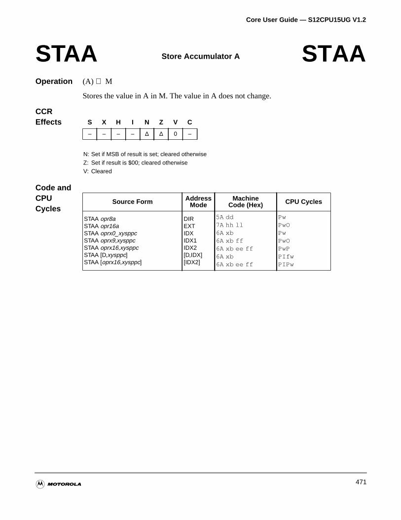
Core User Guide — S12CPU15UG V1.2
Operation (A) ⇒ M
Stores the value in A in M. The value in A does not change.
CCREffects
Code andCPUCycles
STAA Store Accumulator A STAA
S X H I N Z V C
– – – – ∆ ∆ 0 –
N: Set if MSB of result is set; cleared otherwiseZ: Set if result is $00; cleared otherwiseV: Cleared
Source Form AddressMode
MachineCode (Hex) CPU Cycles
STAA opr8aSTAA opr16aSTAA oprx0_xysppcSTAA oprx9,xysppcSTAA oprx16,xysppcSTAA [D,xysppc]STAA [oprx16,xysppc]
DIREXTIDXIDX1IDX2[D,IDX][IDX2]
5A dd7A hh ll6A xb6A xb ff6A xb ee ff6A xb6A xb ee ff
PwPwOPwPwOPwPPIfwPIPw
471
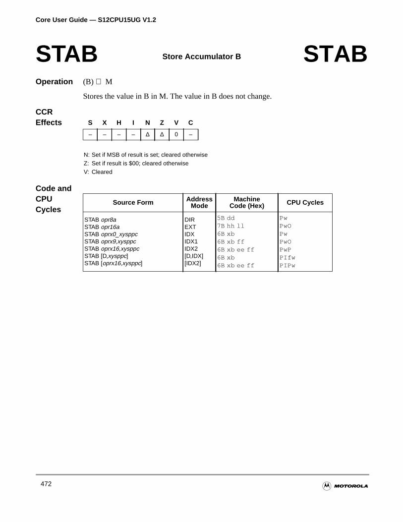
Core User Guide — S12CPU15UG V1.2
Operation (B) ⇒ M
Stores the value in B in M. The value in B does not change.
CCREffects
Code andCPUCycles
STAB Store Accumulator B STAB
S X H I N Z V C
– – – – ∆ ∆ 0 –
N: Set if MSB of result is set; cleared otherwiseZ: Set if result is $00; cleared otherwiseV: Cleared
Source Form AddressMode
MachineCode (Hex) CPU Cycles
STAB opr8aSTAB opr16aSTAB oprx0_xysppcSTAB oprx9,xysppcSTAB oprx16,xysppcSTAB [D,xysppc]STAB [oprx16,xysppc]
DIREXTIDXIDX1IDX2[D,IDX][IDX2]
5B dd7B hh ll6B xb6B xb ff6B xb ee ff6B xb6B xb ee ff
PwPwOPwPwOPwPPIfwPIPw
472
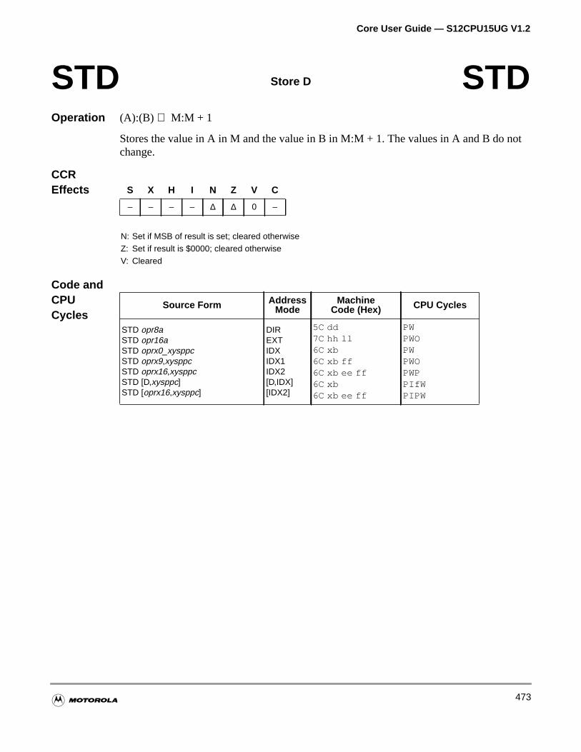
Core User Guide — S12CPU15UG V1.2
ot
Operation (A):(B) ⇒ M:M + 1
Stores the value in A in M and the value in B in M:M + 1. The values in A and B do nchange.
CCREffects
Code andCPUCycles
STD Store D STD
S X H I N Z V C
– – – – ∆ ∆ 0 –
N: Set if MSB of result is set; cleared otherwiseZ: Set if result is $0000; cleared otherwiseV: Cleared
Source Form AddressMode
MachineCode (Hex) CPU Cycles
STD opr8aSTD opr16aSTD oprx0_xysppcSTD oprx9,xysppcSTD oprx16,xysppcSTD [D,xysppc]STD [oprx16,xysppc]
DIREXTIDXIDX1IDX2[D,IDX][IDX2]
5C dd7C hh ll6C xb6C xb ff6C xb ee ff6C xb6C xb ee ff
PWPWOPWPWOPWPPIfWPIPW
473
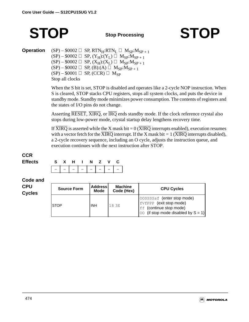
Core User Guide — S12CPU15UG V1.2
henice inrs and
o
s
d
Operation (SP) – $0002⇒ SP, RTNH:RTNL ⇒ MSP:MSP + 1(SP) – $0002⇒ SP, (YH):(YL) ⇒ MSP:MSP + 1(SP) – $0002⇒ SP, (XH):(XL) ⇒ MSP:MSP + 1(SP) – $0002⇒ SP, (B):(A)⇒ MSP:MSP + 1(SP) – $0001⇒ SP, (CCR)⇒ MSPStop all clocks
When the S bit is set, STOP is disabled and operates like a 2-cycle NOP instruction. WS is cleared, STOP stacks CPU registers, stops all system clocks, and puts the devstandby mode. Standby mode minimizes power consumption. The contents of registethe states of I/O pins do not change.
AssertingRESET,XIRQ, or IRQ ends standby mode. If the clock reference crystal alsstops during low-power mode, crystal startup delay lengthens recovery time.
If XIRQ is asserted while the X mask bit = 0 (XIRQ interrupts enabled), execution resumewith a vector fetch for theXIRQ interrupt. If the X mask bit = 1 (XIRQ interrupts disabled),a 2-cycle recovery sequence, including an O cycle, adjusts the instruction queue, anexecution continues with the next instruction after STOP.
CCREffects
Code andCPUCycles
STOP Stop Processing STOP
S X H I N Z V C
– – – – – – – –
Source Form AddressMode
MachineCode (Hex) CPU Cycles
STOP INH 18 3E
OOSSSSsf (enter stop mode)fVfPPP (exit stop mode)ff (continue stop mode)OO (if stop mode disabled by S = 1)
474
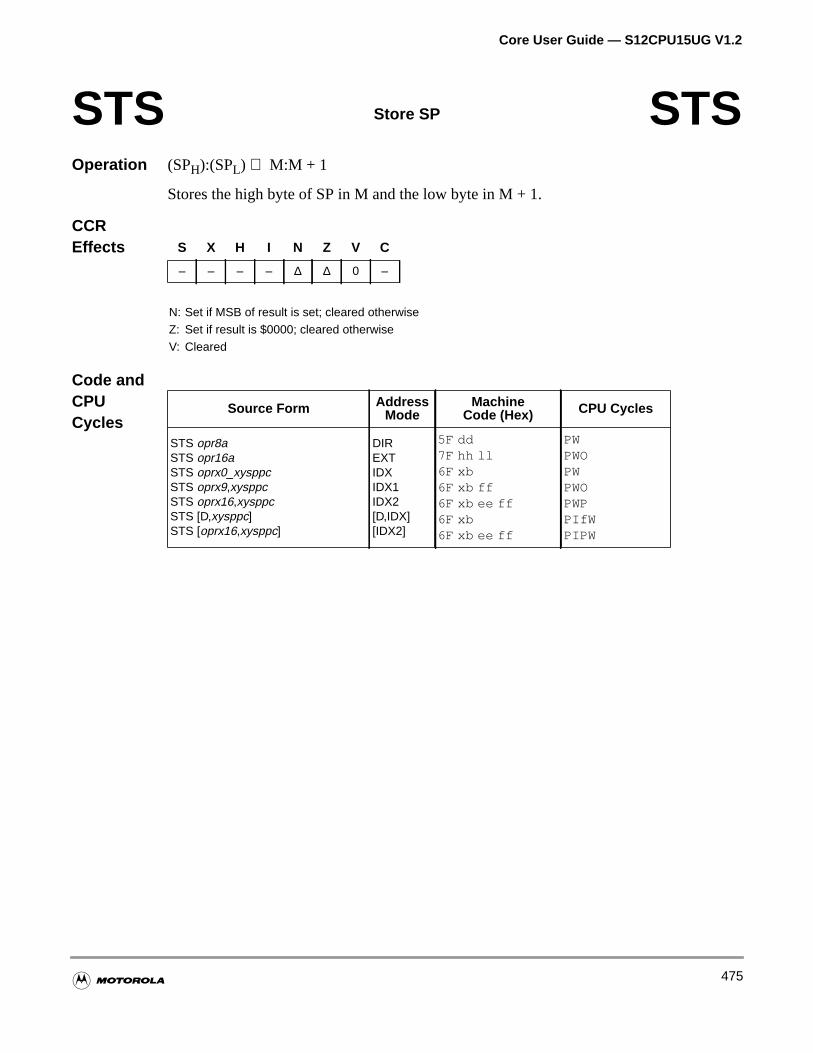
Core User Guide — S12CPU15UG V1.2
Operation (SPH):(SPL) ⇒ M:M + 1
Stores the high byte of SP in M and the low byte in M + 1.
CCREffects
Code andCPUCycles
STS Store SP STS
S X H I N Z V C
– – – – ∆ ∆ 0 –
N: Set if MSB of result is set; cleared otherwiseZ: Set if result is $0000; cleared otherwiseV: Cleared
Source Form AddressMode
MachineCode (Hex) CPU Cycles
STS opr8aSTS opr16aSTS oprx0_xysppcSTS oprx9,xysppcSTS oprx16,xysppcSTS [D,xysppc]STS [oprx16,xysppc]
DIREXTIDXIDX1IDX2[D,IDX][IDX2]
5F dd7F hh ll6F xb6F xb ff6F xb ee ff6F xb6F xb ee ff
PWPWOPWPWOPWPPIfWPIPW
475
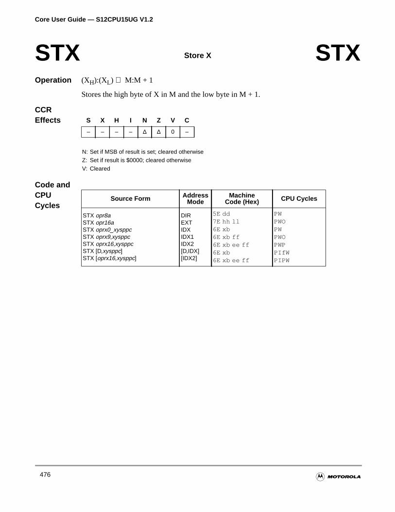
Core User Guide — S12CPU15UG V1.2
Operation (XH):(XL) ⇒ M:M + 1
Stores the high byte of X in M and the low byte in M + 1.
CCREffects
Code andCPUCycles
STX Store X STX
S X H I N Z V C
– – – – ∆ ∆ 0 –
N: Set if MSB of result is set; cleared otherwiseZ: Set if result is $0000; cleared otherwiseV: Cleared
Source Form AddressMode
MachineCode (Hex) CPU Cycles
STX opr8aSTX opr16aSTX oprx0_xysppcSTX oprx9,xysppcSTX oprx16,xysppcSTX [D,xysppc]STX [oprx16,xysppc]
DIREXTIDXIDX1IDX2[D,IDX][IDX2]
5E dd7E hh ll6E xb6E xb ff6E xb ee ff6E xb6E xb ee ff
PWPWOPWPWOPWPPIfWPIPW
476
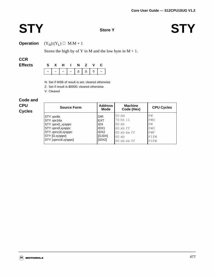
Core User Guide — S12CPU15UG V1.2
Operation (YH):(YL) ⇒ M:M + 1
Stores the high by of Y in M and the low byte in M + 1.
CCREffects
Code andCPUCycles
STY Store Y STY
S X H I N Z V C
– – – – ∆ ∆ 0 –
N: Set if MSB of result is set; cleared otherwiseZ: Set if result is $0000; cleared otherwiseV: Cleared
Source Form AddressMode
MachineCode (Hex) CPU Cycles
STY opr8aSTY opr16aSTY oprx0_xysppcSTY oprx9,xysppcSTY oprx16,xysppcSTY [D,xysppc]STY [oprx16,xysppc]
DIREXTIDXIDX1IDX2[D,IDX][IDX2]
5D dd7D hh ll6D xb6D xb ff6D xb ee ff6D xb6D xb ee ff
PWPWOPWPWOPWPPIfWPIPW
477
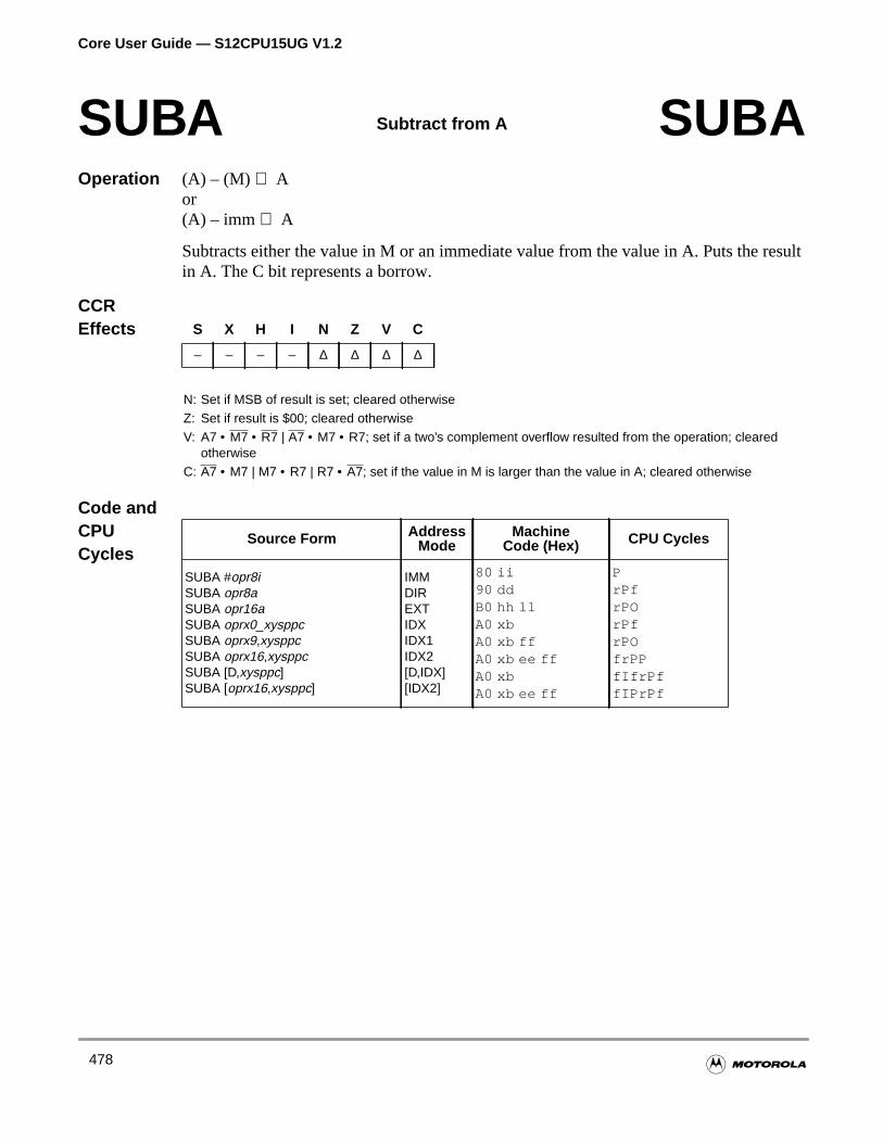
Core User Guide — S12CPU15UG V1.2
esult
Operation (A) – (M) ⇒ Aor(A) – imm ⇒ A
Subtracts either the value in M or an immediate value from the value in A. Puts the rin A. The C bit represents a borrow.
CCREffects
Code andCPUCycles
SUBA Subtract from A SUBA
S X H I N Z V C
– – – – ∆ ∆ ∆ ∆
N: Set if MSB of result is set; cleared otherwiseZ: Set if result is $00; cleared otherwiseV: A7 • M7 • R7 | A7 • M7 • R7; set if a two’s complement overflow resulted from the operation; cleared
otherwiseC: A7 • M7 | M7 • R7 | R7 • A7; set if the value in M is larger than the value in A; cleared otherwise
Source Form AddressMode
MachineCode (Hex) CPU Cycles
SUBA #opr8iSUBA opr8aSUBA opr16aSUBA oprx0_xysppcSUBA oprx9,xysppcSUBA oprx16,xysppcSUBA [D,xysppc]SUBA [oprx16,xysppc]
IMMDIREXTIDXIDX1IDX2[D,IDX][IDX2]
80 ii90 ddB0 hh llA0 xbA0 xb ffA0 xb ee ffA0 xbA0 xb ee ff
PrPfrPOrPfrPOfrPPfIfrPffIPrPf
478
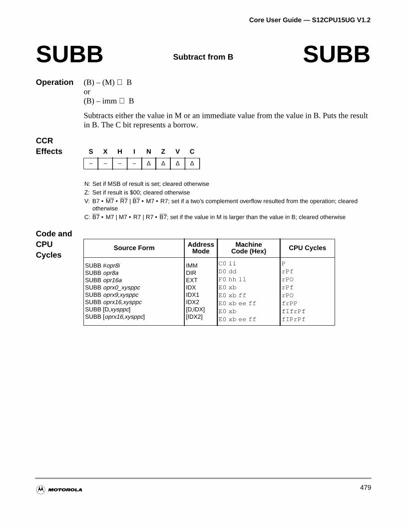
Core User Guide — S12CPU15UG V1.2
esult
Operation (B) – (M) ⇒ Bor(B) – imm⇒ B
Subtracts either the value in M or an immediate value from the value in B. Puts the rin B. The C bit represents a borrow.
CCREffects
Code andCPUCycles
SUBB Subtract from B SUBB
S X H I N Z V C
– – – – ∆ ∆ ∆ ∆
N: Set if MSB of result is set; cleared otherwiseZ: Set if result is $00; cleared otherwiseV: B7 • M7 • R7 | B7 • M7 • R7; set if a two’s complement overflow resulted from the operation; cleared
otherwiseC: B7 • M7 | M7 • R7 | R7 • B7; set if the value in M is larger than the value in B; cleared otherwise
Source Form AddressMode
MachineCode (Hex) CPU Cycles
SUBB #opr8iSUBB opr8aSUBB opr16aSUBB oprx0_xysppcSUBB oprx9,xysppcSUBB oprx16,xysppcSUBB [D,xysppc]SUBB [oprx16,xysppc]
IMMDIREXTIDXIDX1IDX2[D,IDX][IDX2]
C0 iiD0 ddF0 hh llE0 xbE0 xb ffE0 xb ee ffE0 xbE0 xb ee ff
PrPfrPOrPfrPOfrPPfIfrPffIPrPf
479

Core User Guide — S12CPU15UG V1.2
the
Operation (A):(B) – (M):(M + 1) ⇒ A:Bor(A):(B) – imm ⇒ A:B
Subtracts either the value in M:M + 1 or an immediate value from the value in D. Putsresult in D. The C bit represents a borrow.
CCREffects
Code andCPUCycles
SUBD Subtract from D SUBD
S X H I N Z V C
– – – – ∆ ∆ ∆ ∆
N: Set if MSB of result is set; cleared otherwiseZ: Set if result is $0000; cleared otherwiseV: D15 • M15 • R15 | D15 • M15 • R15; set if a two’s complement overflow resulted from the operation;
cleared otherwiseC: D15 • M15 | M15 • R15 | R15 • D15; set if the value in M is larger than the value in D; cleared otherwise
Source Form AddressMode
MachineCode (Hex) CPU Cycles
SUBD #opr16iSUBD opr8aSUBD opr16aSUBD oprx0_xysppcSUBD oprx9,xysspSUBD oprx16,xysppcSUBD [D,xysppc]SUBD [oprx16,xysppc]
IMMDIREXTIDXIDX1IDX2[D,IDX][IDX2]
83 jj kk93 ddB3 hh llA3 xbA3 xb ffA3 xb ee ffA3 xbA3 xb ee ff
PORPfRPORPfRPOfRPPfIfRPffIPRPf
480
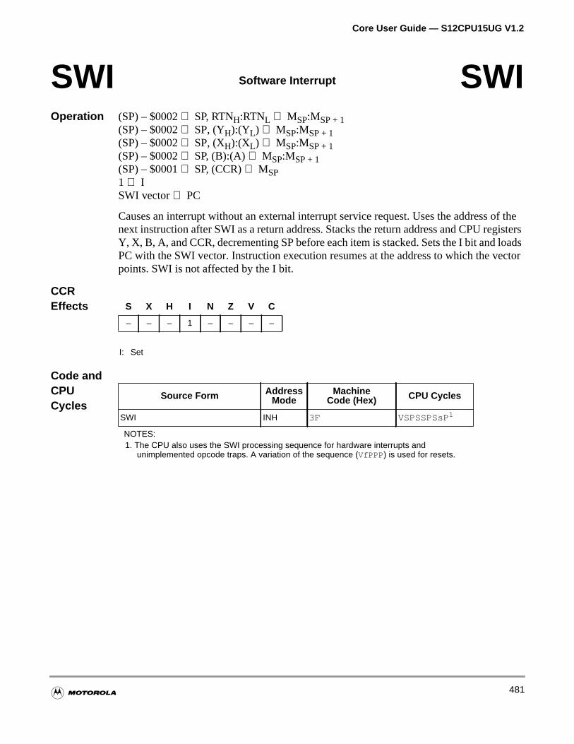
Core User Guide — S12CPU15UG V1.2
of thegistersloadsector
Operation (SP) – $0002⇒ SP, RTNH:RTNL ⇒ MSP:MSP + 1(SP) – $0002⇒ SP, (YH):(YL) ⇒ MSP:MSP + 1(SP) – $0002⇒ SP, (XH):(XL) ⇒ MSP:MSP + 1(SP) – $0002⇒ SP, (B):(A)⇒ MSP:MSP + 1(SP) – $0001⇒ SP, (CCR)⇒ MSP1 ⇒ ISWI vector⇒ PC
Causes an interrupt without an external interrupt service request. Uses the address next instruction after SWI as a return address. Stacks the return address and CPU reY, X, B, A, and CCR, decrementing SP before each item is stacked. Sets the I bit andPC with the SWI vector. Instruction execution resumes at the address to which the vpoints. SWI is not affected by the I bit.
CCREffects
Code andCPUCycles
SWI Software Interrupt SWI
S X H I N Z V C
– – – 1 – – – –
I: Set
Source Form AddressMode
MachineCode (Hex) CPU Cycles
SWI INH 3F VSPSSPSsP1
NOTES:1. The CPU also uses the SWI processing sequence for hardware interrupts and
unimplemented opcode traps. A variation of the sequence (VfPPP) is used for resets.
481
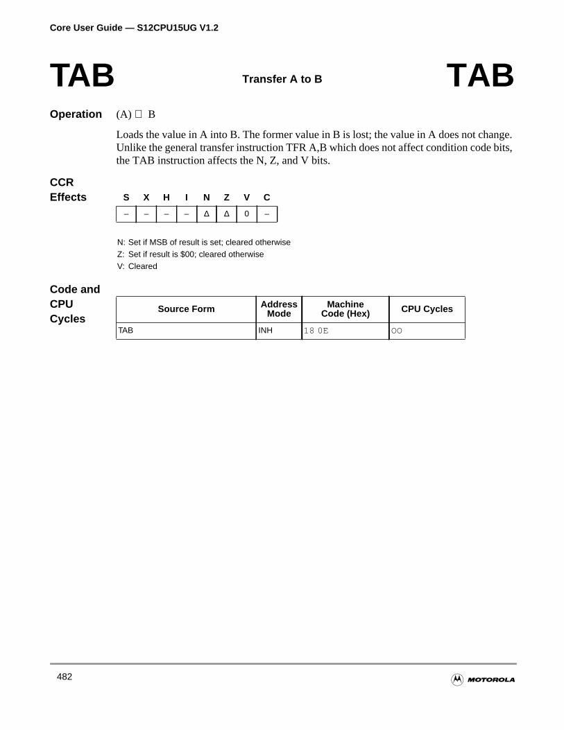
Core User Guide — S12CPU15UG V1.2
ge.its,
Operation (A) ⇒ B
Loads the value in A into B. The former value in B is lost; the value in A does not chanUnlike the general transfer instruction TFR A,B which does not affect condition code bthe TAB instruction affects the N, Z, and V bits.
CCREffects
Code andCPUCycles
TAB Transfer A to B TAB
S X H I N Z V C
– – – – ∆ ∆ 0 –
N: Set if MSB of result is set; cleared otherwiseZ: Set if result is $00; cleared otherwiseV: Cleared
Source Form AddressMode
MachineCode (Hex) CPU Cycles
TAB INH 18 0E OO
482
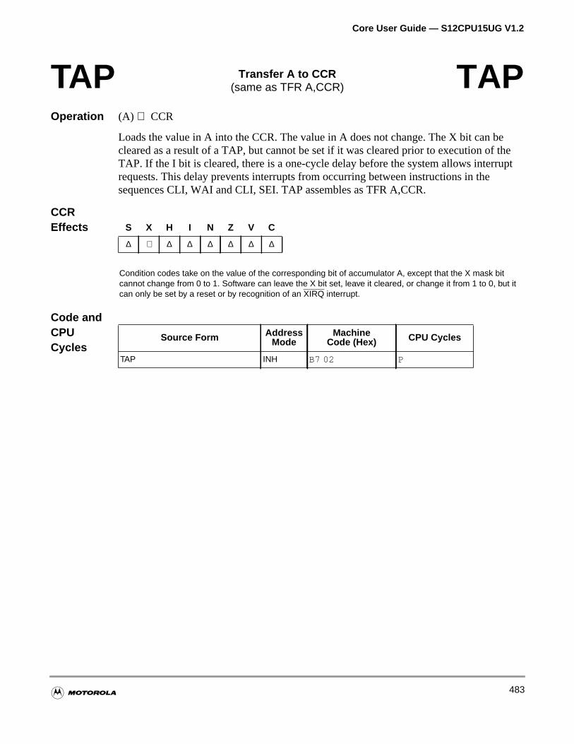
Core User Guide — S12CPU15UG V1.2
e theupt
Operation (A) ⇒ CCR
Loads the value in A into the CCR. The value in A does not change. The X bit can bcleared as a result of a TAP, but cannot be set if it was cleared prior to execution ofTAP. If the I bit is cleared, there is a one-cycle delay before the system allows interrrequests. This delay prevents interrupts from occurring between instructions in thesequences CLI, WAI and CLI, SEI. TAP assembles as TFR A,CCR.
CCREffects
Code andCPUCycles
TAP Transfer A to CCR(same as TFR A,CCR) TAP
S X H I N Z V C
∆ ⇓ ∆ ∆ ∆ ∆ ∆ ∆
Condition codes take on the value of the corresponding bit of accumulator A, except that the X mask bitcannot change from 0 to 1. Software can leave the X bit set, leave it cleared, or change it from 1 to 0, but itcan only be set by a reset or by recognition of an XIRQ interrupt.
Source Form AddressMode
MachineCode (Hex) CPU Cycles
TAP INH B7 02 P
483
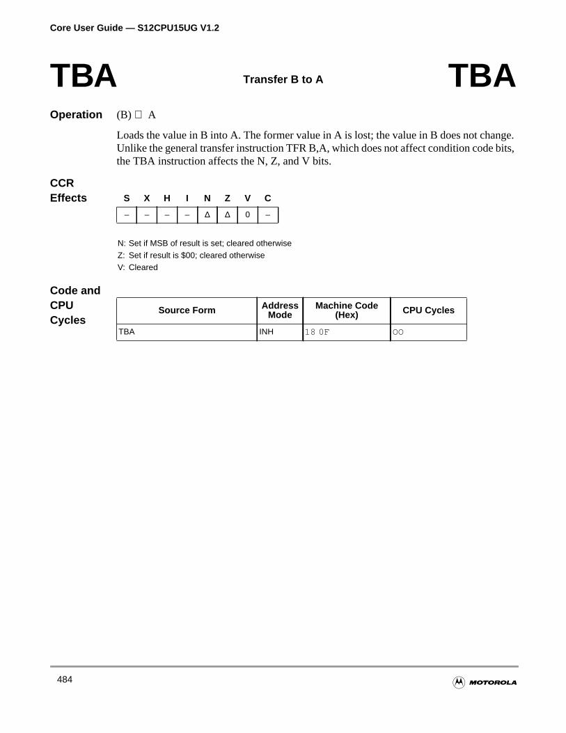
Core User Guide — S12CPU15UG V1.2
ge.its,
Operation (B) ⇒ A
Loads the value in B into A. The former value in A is lost; the value in B does not chanUnlike the general transfer instruction TFR B,A, which does not affect condition code bthe TBA instruction affects the N, Z, and V bits.
CCREffects
Code andCPUCycles
TBA Transfer B to A TBA
S X H I N Z V C
– – – – ∆ ∆ 0 –
N: Set if MSB of result is set; cleared otherwiseZ: Set if result is $00; cleared otherwiseV: Cleared
Source Form AddressMode
Machine Code(Hex) CPU Cycles
TBA INH 18 0F OO
484
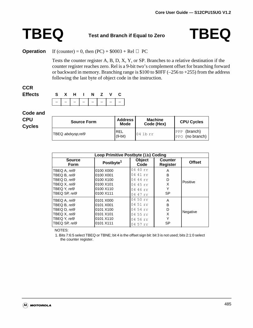
Core User Guide — S12CPU15UG V1.2
heard
ress
Operation If (counter) = 0, then (PC) + $0003 + Rel⇒ PC
Tests the counter register A, B, D, X, Y, or SP. Branches to a relative destination if tcounter register reaches zero. Rel is a 9-bit two’s complement offset for branching forwor backward in memory. Branching range is $100 to $0FF (–256 to +255) from the addfollowing the last byte of object code in the instruction.
CCREffects
Code andCPUCycles
TBEQ Test and Branch if Equal to Zero TBEQ
S X H I N Z V C
– – – – – – – –
Source Form AddressMode
MachineCode (Hex) CPU Cycles
TBEQ abdxysp,rel9REL(9-bit)
04 lb rrPPP (branch)PPO (no branch)
Loop Primitive Postbyte ( lb ) CodingSourceForm Postbyte 1
NOTES:1. Bits 7:6:5 select TBEQ or TBNE; bit 4 is the offset sign bit: bit 3 is not used; bits 2:1:0 select
the counter register.
ObjectCode
CounterRegister Offset
TBEQ A, rel9TBEQ B, rel9TBEQ D, rel9TBEQ X, rel9TBEQ Y, rel9TBEQ SP, rel9
0100 X0000100 X0010100 X1000100 X1010100 X1100100 X111
04 40 rr04 41 rr04 44 rr04 45 rr04 46 rr04 47 rr
ABDXY
SP
Positive
TBEQ A, rel9TBEQ B, rel9TBEQ D, rel9TBEQ X, rel9TBEQ Y, rel9TBEQ SP, rel9
0101 X0000101 X0010101 X1000101 X1010101 X1100101 X111
04 50 rr04 51 rr04 54 rr04 55 rr04 56 rr04 57 rr
ABDXY
SP
Negative
485
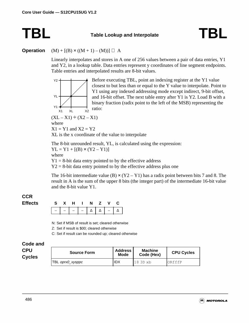
Core User Guide — S12CPU15UG V1.2
s, Y1oints.
t toet, a
elue
Operation (M) + [(B) × ((M + 1) – (M))] ⇒ A
Linearly interpolates and stores in A one of 256 values between a pair of data entrieand Y2, in a lookup table. Data entries represent y coordinates of line segment endpTable entries and interpolated results are 8-bit values.
Before executing TBL, point an indexing register at the Y1 valueclosest to but less than or equal to the Y value to interpolate. PoinY1 using any indexed addressing mode except indirect, 9-bit offsand 16-bit offset. The next table entry after Y1 is Y2. Load B withbinary fraction (radix point to the left of the MSB) representing theratio:
(XL – X1) ÷ (X2 – X1)whereX1 = Y1 and X2 = Y2XL is the x coordinate of the value to interpolate
The 8-bit unrounded result, YL, is calculated using the expression:YL = Y1 + [(B) × (Y2 – Y1)]whereY1 = 8-bit data entry pointed to by the effective addressY2 = 8-bit data entry pointed to by the effective address plus one
The 16-bit intermediate value (B)× (Y2 – Y1) has a radix point between bits 7 and 8. Thresult in A is the sum of the upper 8 bits (the integer part) of the intermediate 16-bit vaand the 8-bit value Y1.
CCREffects
Code andCPUCycles
TBL Table Lookup and Interpolate TBL
X1 X2Y1
Y2
XL
YL
S X H I N Z V C
– – – – ∆ ∆ – ∆
N: Set if MSB of result is set; cleared otherwiseZ: Set if result is $00; cleared otherwiseC: Set if result can be rounded up; cleared otherwise
Source Form AddressMode
MachineCode (Hex) CPU Cycles
TBL oprx0_xysppc IDX 18 3D xb ORfffP
486

Core User Guide — S12CPU15UG V1.2
heardress
Operation If (counter)≠ 0, then (PC) + $0003 + Rel⇒ PC
Tests the counter register A, B, D, X, Y, or SP. Branches to a relative destination if tcounter does not reach zero. Rel is a 9-bit two’s complement offset for branching forwor backward in memory. Branching range is $100 to $0FF (–256 to +255) from the addfollowing the last byte of object code in the instruction.
CCREffects
Code andCPUCycles
TBNE Test and Branch if Not Equal to Zero TBNE
S X H I N Z V C
– – – – – – – –
Source Form AddressMode
MachineCode (Hex) CPU Cycles
TBNE abdxysp,rel9REL(9-bit)
04 lb rrPPP (branch)PPO (no branch)
Loop Primitive Postbyte ( lb ) CodingSourceForm Postbyte 1
NOTES:1. Bits 7:6:5 select TBEQ or TBNE; bit 4 is the offset sign bit: bit 3 is not used; bits 2:1:0 select
the counter register.
ObjectCode
CounterRegister Offset
TBNE A, rel9TBNE B, rel9TBNE D, rel9TBNE X, rel9TBNE Y, rel9TBNE SP, rel9
0110 X0000110 X0010110 X1000110 X1010110 X1100110 X111
04 60 rr04 61 rr04 64 rr04 65 rr04 66 rr04 67 rr
ABDXY
SP
Positive
TBNE A, rel9TBNE B, rel9TBNE D, rel9TBNE X, rel9TBNE Y, rel9TBNE SP, rel9
0111 X0000111 X0010111 X1000111 X1010111 X1100111 X111
04 70 rr04 71 rr04 74 rr04 75 rr04 76 rr04 77 rr
ABDXY
SP
Negative
487
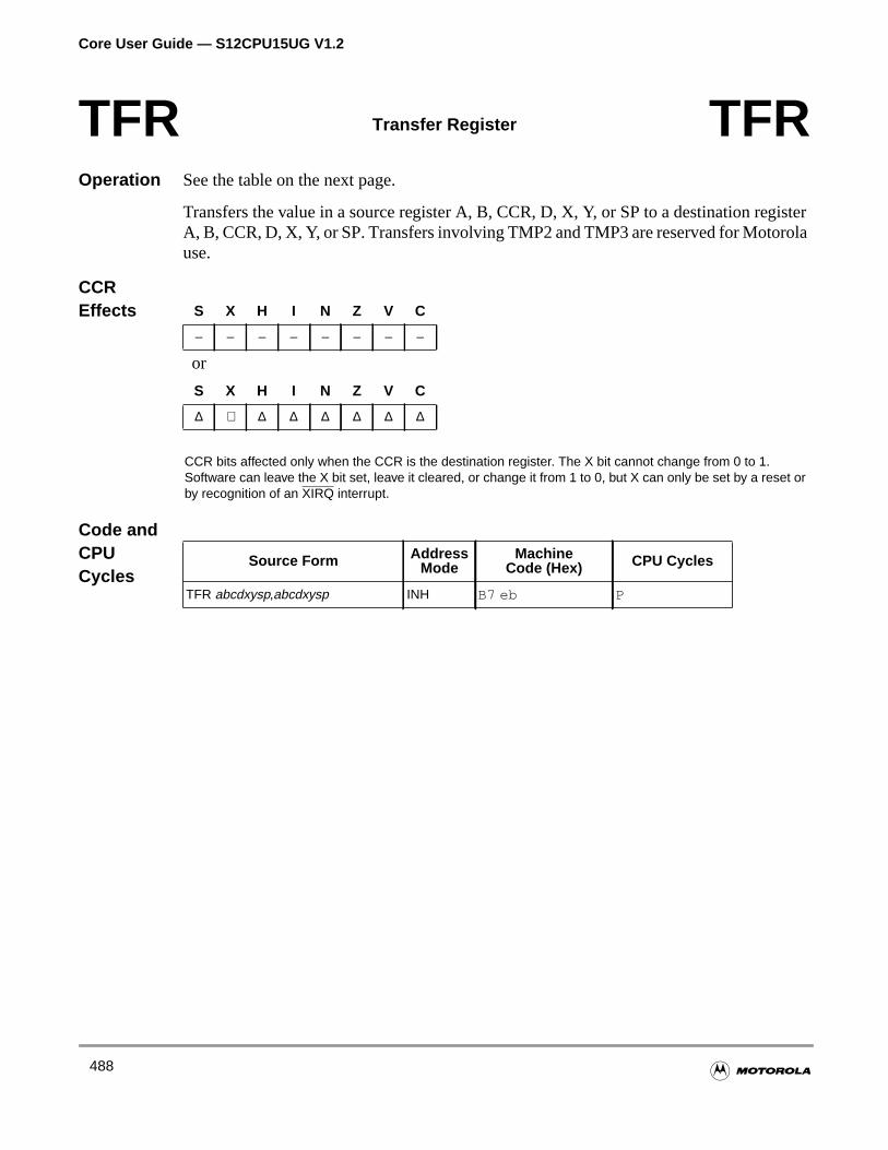
Core User Guide — S12CPU15UG V1.2
isterola
Operation See the table on the next page.
Transfers the value in a source register A, B, CCR, D, X, Y, or SP to a destination regA, B, CCR, D, X, Y, or SP. Transfers involving TMP2 and TMP3 are reserved for Motoruse.
CCREffects
Code andCPUCycles
TFR Transfer Register TFR
S X H I N Z V C
– – – – – – – –
or
S X H I N Z V C
∆ ⇓ ∆ ∆ ∆ ∆ ∆ ∆
CCR bits affected only when the CCR is the destination register. The X bit cannot change from 0 to 1.Software can leave the X bit set, leave it cleared, or change it from 1 to 0, but X can only be set by a reset orby recognition of an XIRQ interrupt.
Source Form AddressMode
MachineCode (Hex) CPU Cycles
TFR abcdxysp,abcdxysp INH B7 eb P
488
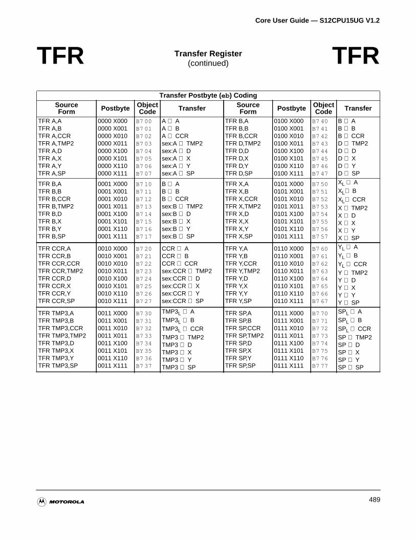
Core User Guide — S12CPU15UG V1.2
TFR Transfer Register(continued) TFR
Transfer Postbyte ( eb) CodingSourceForm Postbyte Object
Code Transfer SourceForm Postbyte Object
Code Transfer
TFR A,ATFR A,BTFR A,CCRTFR A,TMP2TFR A,DTFR A,XTFR A,YTFR A,SP
0000 X0000000 X0010000 X0100000 X0110000 X1000000 X1010000 X1100000 X111
B7 00B7 01B7 02B7 03B7 04B7 05B7 06B7 07
A ⇒ AA ⇒ BA ⇒ CCRsex:A ⇒ TMP2sex:A ⇒ Dsex:A ⇒ Xsex:A ⇒ Ysex:A ⇒ SP
TFR B,ATFR B,BTFR B,CCRTFR D,TMP2TFR D,DTFR D,XTFR D,YTFR D,SP
0100 X0000100 X0010100 X0100100 X0110100 X1000100 X1010100 X1100100 X111
B7 40B7 41B7 42B7 43B7 44B7 45B7 46B7 47
B ⇒ AB ⇒ BB ⇒ CCRD ⇒ TMP2D ⇒ DD ⇒ XD ⇒ YD ⇒ SP
TFR B,ATFR B,BTFR B,CCRTFR B,TMP2TFR B,DTFR B,XTFR B,YTFR B,SP
0001 X0000001 X0010001 X0100001 X0110001 X1000001 X1010001 X1100001 X111
B7 10B7 11B7 12B7 13B7 14B7 15B7 16B7 17
B ⇒ AB ⇒ BB ⇒ CCRsex:B ⇒ TMP2sex:B ⇒ Dsex:B ⇒ Xsex:B ⇒ Ysex:B ⇒ SP
TFR X,ATFR X,BTFR X,CCRTFR X,TMP2TFR X,DTFR X,XTFR X,YTFR X,SP
0101 X0000101 X0010101 X0100101 X0110101 X1000101 X1010101 X1100101 X111
B7 50B7 51B7 52B7 53B7 54B7 55B7 56B7 57
XL ⇒ AXL⇒ BXL⇒ CCRX ⇒ TMP2X ⇒ DX ⇒ XX ⇒ YX ⇒ SP
TFR CCR,ATFR CCR,BTFR CCR,CCRTFR CCR,TMP2TFR CCR,DTFR CCR,XTFR CCR,YTFR CCR,SP
0010 X0000010 X0010010 X0100010 X0110010 X1000010 X1010010 X1100010 X111
B7 20B7 21B7 22B7 23B7 24B7 25B7 26B7 27
CCR ⇒ ACCR ⇒ BCCR ⇒ CCRsex:CCR ⇒ TMP2sex:CCR ⇒ Dsex:CCR ⇒ Xsex:CCR ⇒ Ysex:CCR ⇒ SP
TFR Y,ATFR Y,BTFR Y,CCRTFR Y,TMP2TFR Y,DTFR Y,XTFR Y,YTFR Y,SP
0110 X0000110 X0010110 X0100110 X0110110 X1000110 X1010110 X1100110 X111
B7 60B7 61B7 62B7 63B7 64B7 65B7 66B7 67
YL ⇒ AYL ⇒ BYL ⇒ CCRY ⇒ TMP2Y ⇒ DY ⇒ XY ⇒ YY ⇒ SP
TFR TMP3,ATFR TMP3,BTFR TMP3,CCRTFR TMP3,TMP2TFR TMP3,DTFR TMP3,XTFR TMP3,YTFR TMP3,SP
0011 X0000011 X0010011 X0100011 X0110011 X1000011 X1010011 X1100011 X111
B7 30B7 31B7 32B7 33B7 34BY 35B7 36B7 37
TMP3L ⇒ ATMP3L ⇒ BTMP3L ⇒ CCRTMP3 ⇒ TMP2TMP3 ⇒ DTMP3 ⇒ XTMP3 ⇒ YTMP3 ⇒ SP
TFR SP,ATFR SP,BTFR SP,CCRTFR SP,TMP2TFR SP,DTFR SP,XTFR SP,YTFR SP,SP
0111 X0000111 X0010111 X0100111 X0110111 X1000111 X1010111 X1100111 X111
B7 70B7 71B7 72B7 73B7 74B7 75B7 76B7 77
SPL ⇒ ASPL ⇒ BSPL ⇒ CCRSP ⇒ TMP2SP ⇒ DSP ⇒ XSP ⇒ YSP ⇒ SP
489
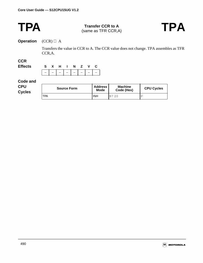
Core User Guide — S12CPU15UG V1.2
TFR
Operation (CCR)⇒ A
Transfers the value in CCR to A. The CCR value does not change. TPA assembles asCCR,A.
CCREffects
Code andCPUCycles
TPA Transfer CCR to A(same as TFR CCR,A) TPA
S X H I N Z V C
– – – – – – – –
Source Form AddressMode
MachineCode (Hex) CPU Cycles
TPA INH B7 20 P
490
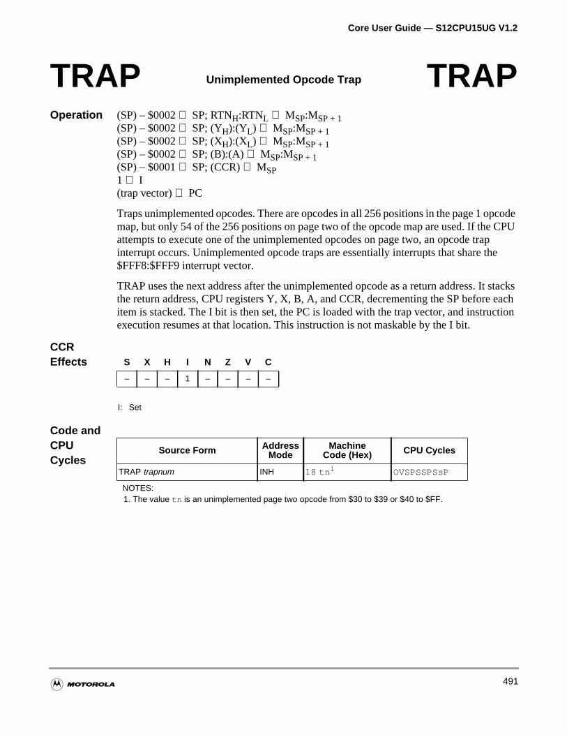
Core User Guide — S12CPU15UG V1.2
pcodeCPUphe
stacks eachction
Operation (SP) – $0002⇒ SP; RTNH:RTNL ⇒ MSP:MSP + 1(SP) – $0002⇒ SP; (YH):(YL) ⇒ MSP:MSP + 1(SP) – $0002⇒ SP; (XH):(XL) ⇒ MSP:MSP + 1(SP) – $0002⇒ SP; (B):(A)⇒ MSP:MSP + 1(SP) – $0001⇒ SP; (CCR)⇒ MSP1 ⇒ I(trap vector)⇒ PC
Traps unimplemented opcodes. There are opcodes in all 256 positions in the page 1 omap, but only 54 of the 256 positions on page two of the opcode map are used. If theattempts to execute one of the unimplemented opcodes on page two, an opcode trainterrupt occurs. Unimplemented opcode traps are essentially interrupts that share t$FFF8:$FFF9 interrupt vector.
TRAP uses the next address after the unimplemented opcode as a return address. Itthe return address, CPU registers Y, X, B, A, and CCR, decrementing the SP beforeitem is stacked. The I bit is then set, the PC is loaded with the trap vector, and instruexecution resumes at that location. This instruction is not maskable by the I bit.
CCREffects
Code andCPUCycles
TRAP Unimplemented Opcode Trap TRAP
S X H I N Z V C
– – – 1 – – – –
I: Set
Source Form AddressMode
MachineCode (Hex) CPU Cycles
TRAP trapnum INH 18 tn 1
NOTES:1. The value tn is an unimplemented page two opcode from $30 to $39 or $40 to $FF.
OVSPSSPSsP
491
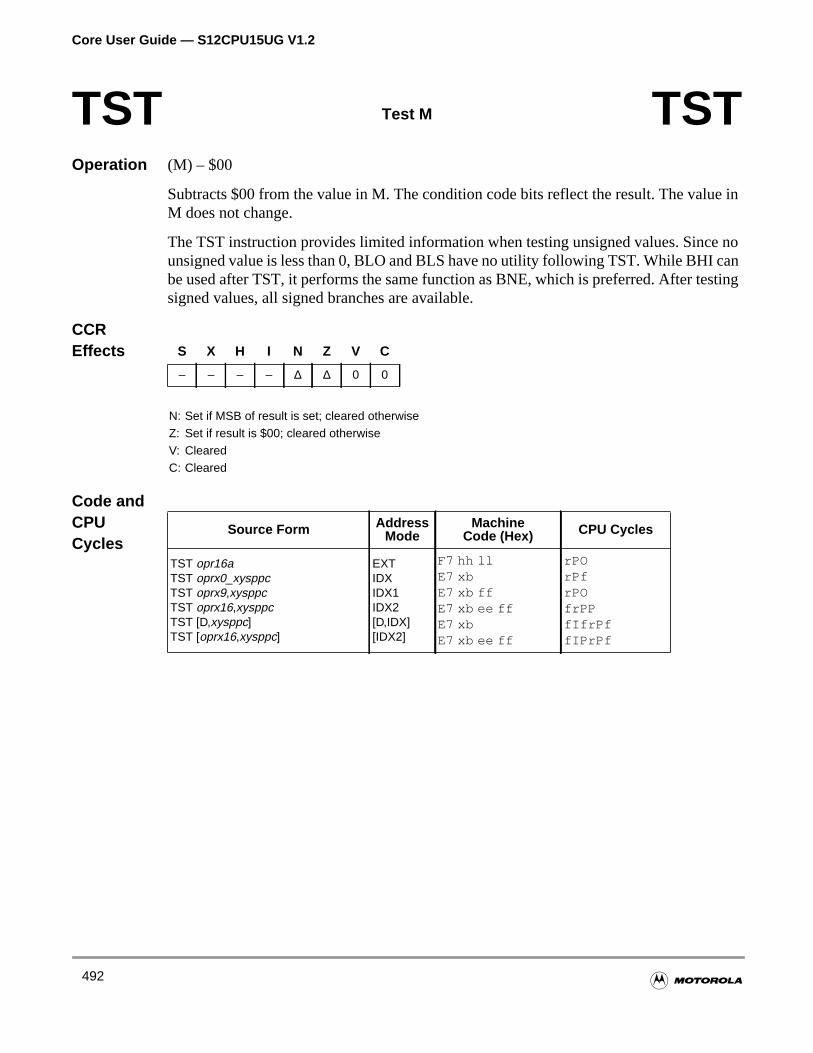
Core User Guide — S12CPU15UG V1.2
e in
noanting
Operation (M) – $00
Subtracts $00 from the value in M. The condition code bits reflect the result. The valuM does not change.
The TST instruction provides limited information when testing unsigned values. Sinceunsigned value is less than 0, BLO and BLS have no utility following TST. While BHI cbe used after TST, it performs the same function as BNE, which is preferred. After tessigned values, all signed branches are available.
CCREffects
Code andCPUCycles
TST Test M TST
S X H I N Z V C
– – – – ∆ ∆ 0 0
N: Set if MSB of result is set; cleared otherwiseZ: Set if result is $00; cleared otherwiseV: ClearedC: Cleared
Source Form AddressMode
MachineCode (Hex) CPU Cycles
TST opr16aTST oprx0_xysppcTST oprx9,xysppcTST oprx16,xysppcTST [D,xysppc]TST [oprx16,xysppc]
EXTIDXIDX1IDX2[D,IDX][IDX2]
F7 hh llE7 xbE7 xb ffE7 xb ee ffE7 xbE7 xb ee ff
rPOrPfrPOfrPPfIfrPffIPrPf
492
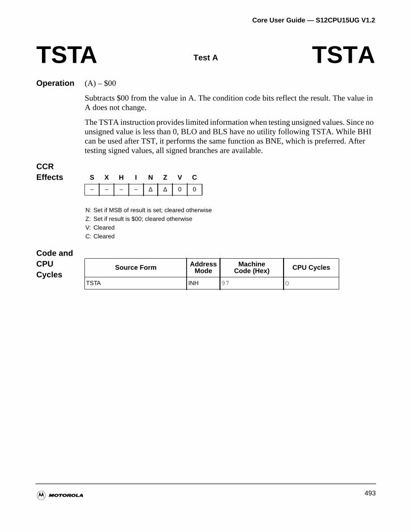
Core User Guide — S12CPU15UG V1.2
ue in
e noHIter
Operation (A) – $00
Subtracts $00 from the value in A. The condition code bits reflect the result. The valA does not change.
The TSTA instruction provides limited information when testing unsigned values. Sincunsigned value is less than 0, BLO and BLS have no utility following TSTA. While Bcan be used after TST, it performs the same function as BNE, which is preferred. Aftesting signed values, all signed branches are available.
CCREffects
Code andCPUCycles
TSTA Test A TSTA
S X H I N Z V C
– – – – ∆ ∆ 0 0
N: Set if MSB of result is set; cleared otherwiseZ: Set if result is $00; cleared otherwiseV: ClearedC: Cleared
Source Form AddressMode
MachineCode (Hex) CPU Cycles
TSTA INH 97 O
493
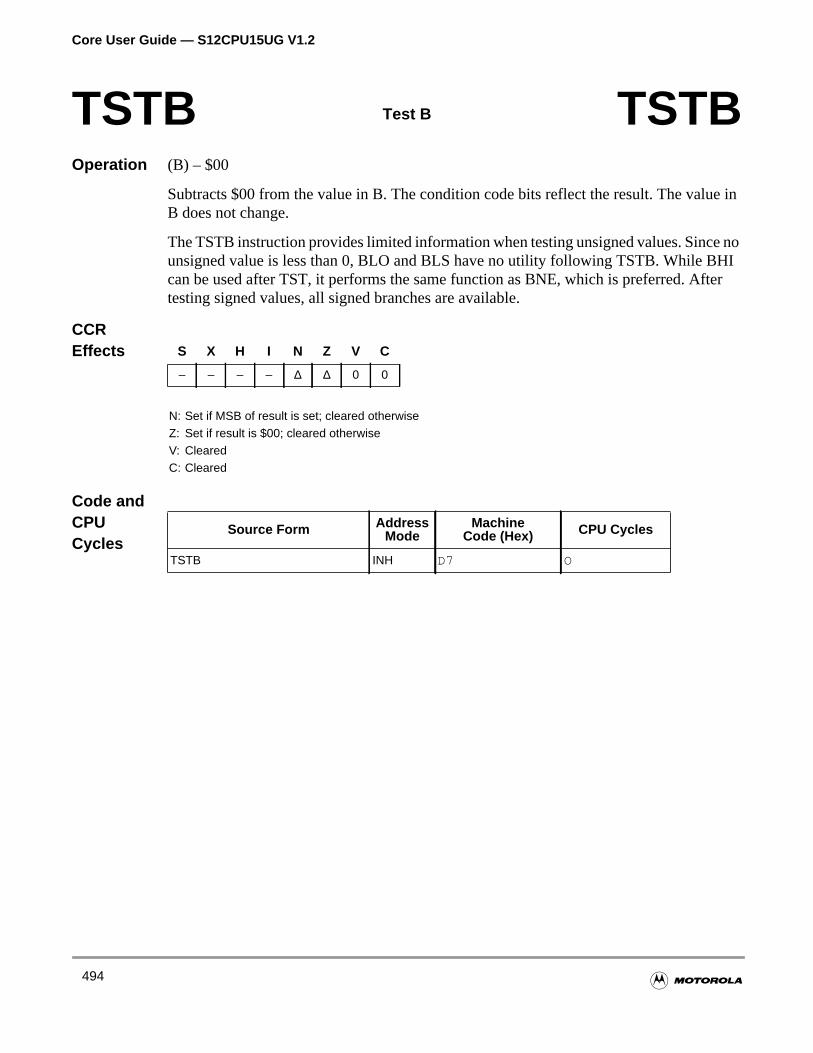
Core User Guide — S12CPU15UG V1.2
ue in
e noHIter
Operation (B) – $00
Subtracts $00 from the value in B. The condition code bits reflect the result. The valB does not change.
The TSTB instruction provides limited information when testing unsigned values. Sincunsigned value is less than 0, BLO and BLS have no utility following TSTB. While Bcan be used after TST, it performs the same function as BNE, which is preferred. Aftesting signed values, all signed branches are available.
CCREffects
Code andCPUCycles
TSTB Test B TSTB
S X H I N Z V C
– – – – ∆ ∆ 0 0
N: Set if MSB of result is set; cleared otherwiseZ: Set if result is $00; cleared otherwiseV: ClearedC: Cleared
Source Form AddressMode
MachineCode (Hex) CPU Cycles
TSTB INH D7 O
494
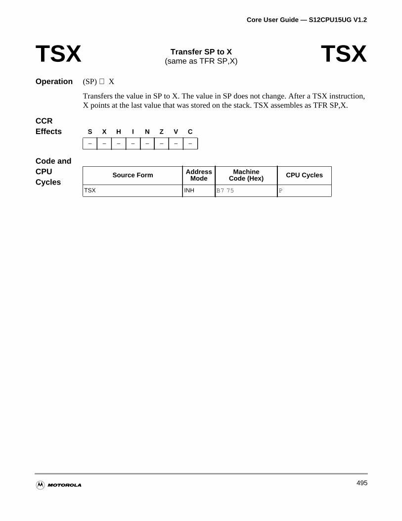
Core User Guide — S12CPU15UG V1.2
tion,.
Operation (SP)⇒ X
Transfers the value in SP to X. The value in SP does not change. After a TSX instrucX points at the last value that was stored on the stack. TSX assembles as TFR SP,X
CCREffects
Code andCPUCycles
TSX Transfer SP to X(same as TFR SP,X) TSX
S X H I N Z V C
– – – – – – – –
Source Form AddressMode
MachineCode (Hex) CPU Cycles
TSX INH B7 75 P
495
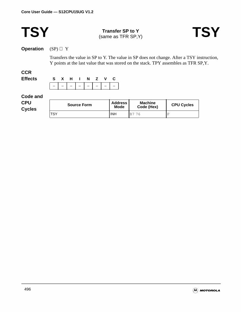
Core User Guide — S12CPU15UG V1.2
ction,.
Operation (SP)⇒ Y
Transfers the value in SP to Y. The value in SP does not change. After a TSY instruY points at the last value that was stored on the stack. TPY assembles as TFR SP,Y
CCREffects
Code andCPUCycles
TSY Transfer SP to Y(same as TFR SP,Y) TSY
S X H I N Z V C
– – – – – – – –
Source Form AddressMode
MachineCode (Hex) CPU Cycles
TSY INH B7 76 P
496
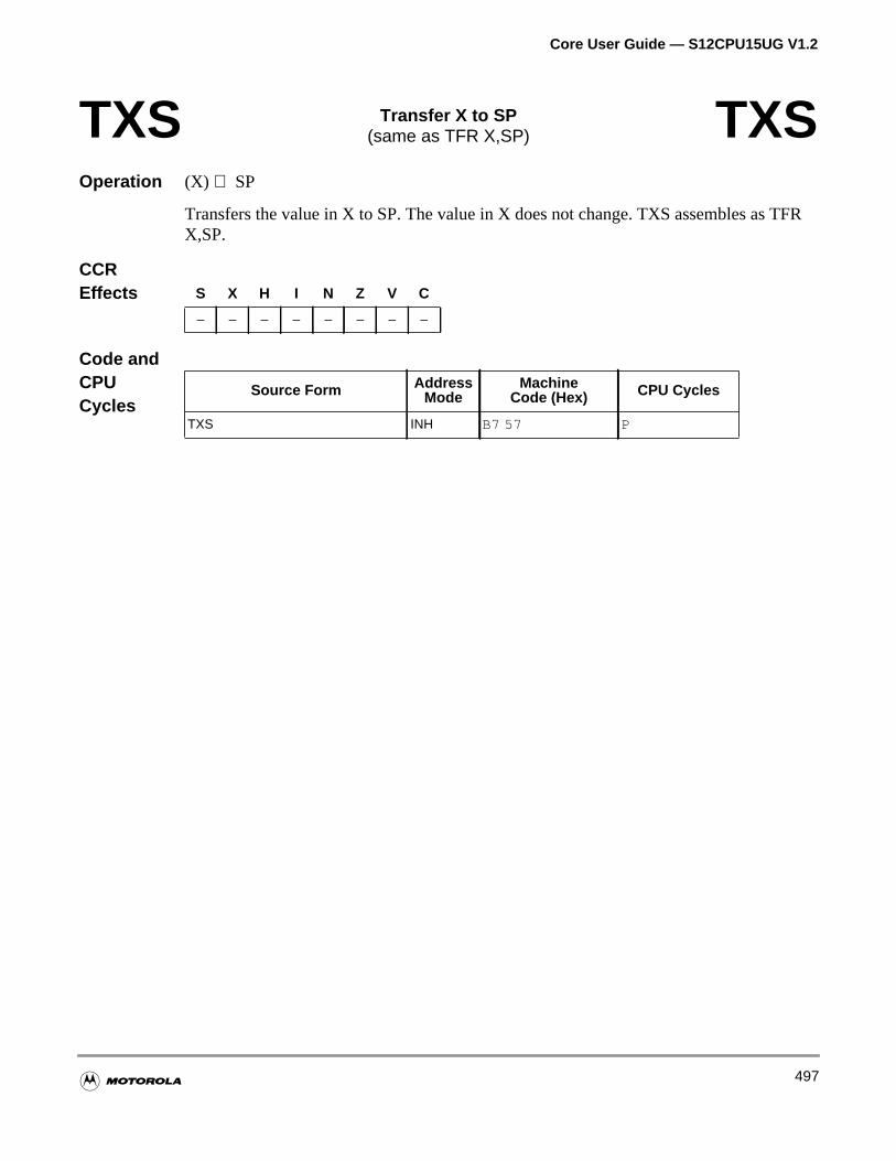
Core User Guide — S12CPU15UG V1.2
TFR
Operation (X) ⇒ SP
Transfers the value in X to SP. The value in X does not change. TXS assembles asX,SP.
CCREffects
Code andCPUCycles
TXS Transfer X to SP(same as TFR X,SP) TXS
S X H I N Z V C
– – – – – – – –
Source Form AddressMode
MachineCode (Hex) CPU Cycles
TXS INH B7 57 P
497
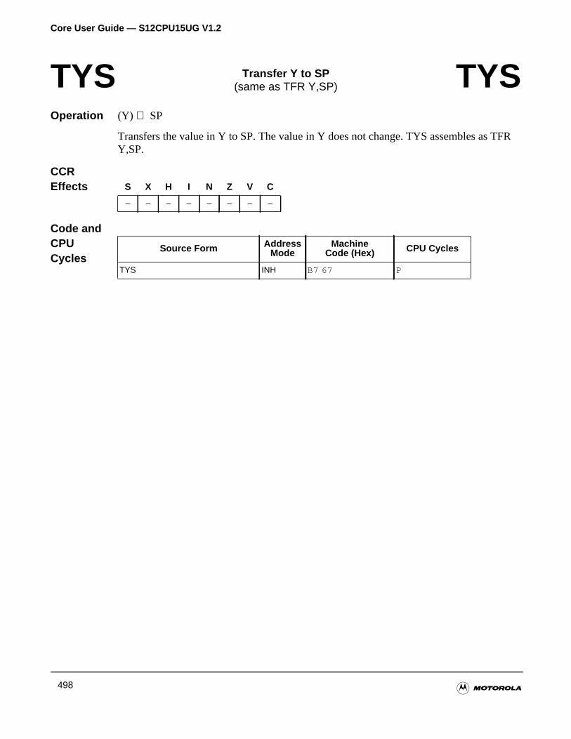
Core User Guide — S12CPU15UG V1.2
TFR
Operation (Y) ⇒ SP
Transfers the value in Y to SP. The value in Y does not change. TYS assembles asY,SP.
CCREffects
Code andCPUCycles
TYS Transfer Y to SP(same as TFR Y,SP) TYS
S X H I N Z V C
– – – – – – – –
Source Form AddressMode
MachineCode (Hex) CPU Cycles
TYS INH B7 67 P
498
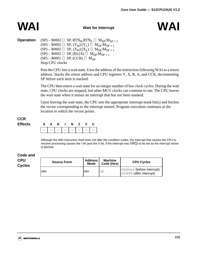
Core User Guide — S12CPU15UG V1.2
turnenting
waitaves
tchese
Operation (SP) – $0002⇒ SP, RTNH:RTNL ⇒ MSP:MSP + 1(SP) – $0002⇒ SP, (YH):(YL) ⇒ MSP:MSP + 1(SP) – $0002⇒ SP, (XH):(XL) ⇒ MSP:MSP + 1(SP) – $0002⇒ SP, (B):(A)⇒ MSP:MSP + 1(SP) – $0001⇒ SP, (CCR)⇒ MSPStop CPU clocks
Puts the CPU into a wait state. Uses the address of the instruction following WAI as a readdress. Stacks the return address and CPU registers Y, X, B, A, and CCR, decremSP before each item is stacked.
The CPU then enters a wait state for an integer number of bus clock cycles. During thestate, CPU clocks are stopped, but other MCU clocks can continue to run. The CPU lethe wait state when it senses an interrupt that has not been masked.
Upon leaving the wait state, the CPU sets the appropriate interrupt mask bit(s) and fethe vector corresponding to the interrupt sensed. Program execution continues at thlocation to which the vector points.
CCREffects
Code andCPUCycles
WAI Wait for Interrupt WAI
S X H I N Z V C
– – – – – – – –
Although the WAI instruction itself does not alter the condition codes, the interrupt that causes the CPU toresume processing causes the I bit (and the X bit, if the interrupt was XIRQ) to be set as the interrupt vectoris fetched.
Source Form AddressMode
MachineCode (Hex) CPU Cycles
WAI INH 3EOSSSSsf (before interrupt)fVfPPP (after interrupt)
499
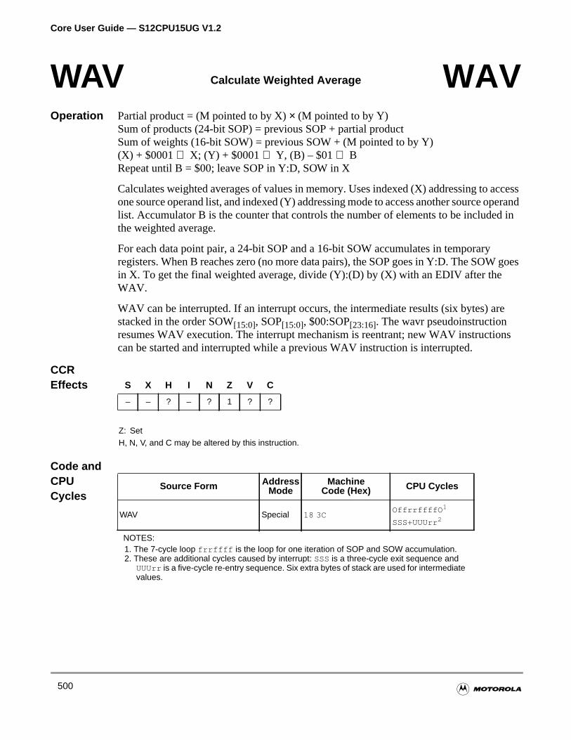
Core User Guide — S12CPU15UG V1.2
ccessperandd in
goes
re
ns
Operation Partial product = (M pointed to by X)× (M pointed to by Y)Sum of products (24-bit SOP) = previous SOP + partial productSum of weights (16-bit SOW) = previous SOW + (M pointed to by Y)(X) + $0001⇒ X; (Y) + $0001⇒ Y, (B) – $01⇒ BRepeat until B = $00; leave SOP in Y:D, SOW in X
Calculates weighted averages of values in memory. Uses indexed (X) addressing to aone source operand list, and indexed (Y) addressing mode to access another source olist. Accumulator B is the counter that controls the number of elements to be includethe weighted average.
For each data point pair, a 24-bit SOP and a 16-bit SOW accumulates in temporaryregisters. When B reaches zero (no more data pairs), the SOP goes in Y:D. The SOWin X. To get the final weighted average, divide (Y):(D) by (X) with an EDIV after theWAV.
WAV can be interrupted. If an interrupt occurs, the intermediate results (six bytes) astacked in the order SOW[15:0], SOP[15:0], $00:SOP[23:16]. The wavr pseudoinstructionresumes WAV execution. The interrupt mechanism is reentrant; new WAV instructiocan be started and interrupted while a previous WAV instruction is interrupted.
CCREffects
Code andCPUCycles
WAV Calculate Weighted Average WAV
S X H I N Z V C
– – ? – ? 1 ? ?
Z: SetH, N, V, and C may be altered by this instruction.
Source Form AddressMode
MachineCode (Hex) CPU Cycles
WAV Special 18 3COffrrffffO 1
SSS+UUUrr2
NOTES:1. The 7-cycle loop frrffff is the loop for one iteration of SOP and SOW accumulation.2. These are additional cycles caused by interrupt: SSS is a three-cycle exit sequence and
UUUrr is a five-cycle re-entry sequence. Six extra bytes of stack are used for intermediatevalues.
500
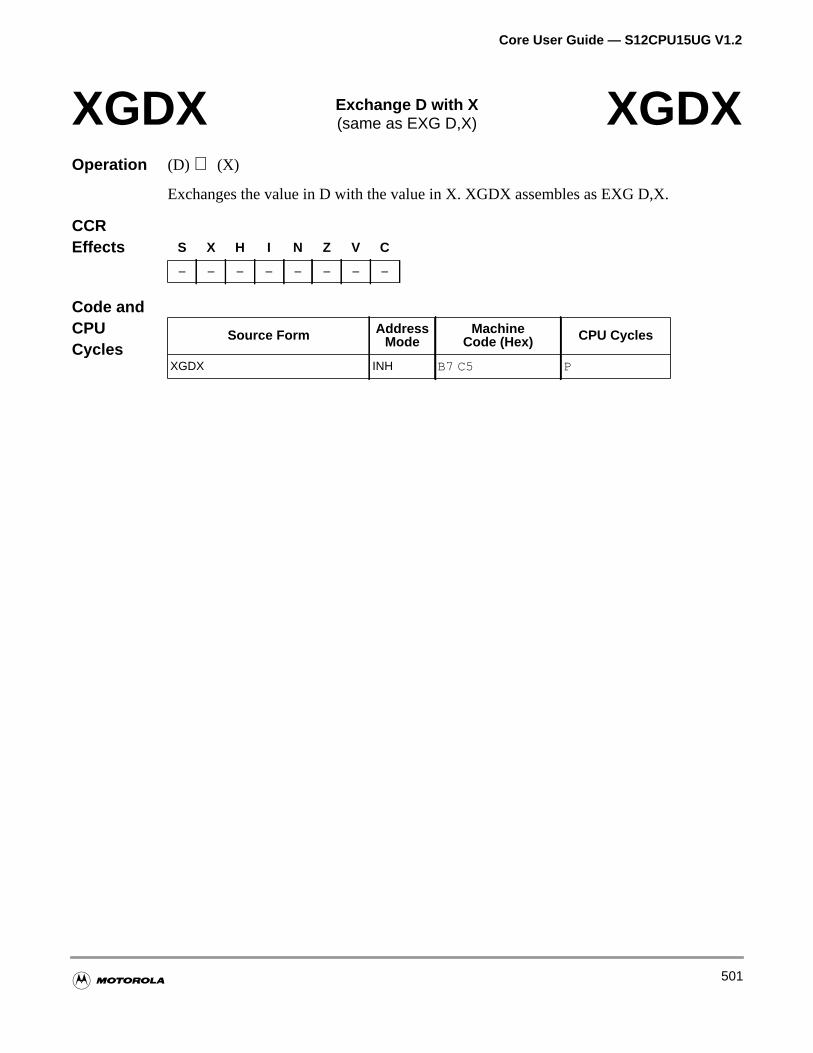
Core User Guide — S12CPU15UG V1.2
Operation (D) ⇔ (X)
Exchanges the value in D with the value in X. XGDX assembles as EXG D,X.
CCREffects
Code andCPUCycles
XGDX Exchange D with X(same as EXG D,X) XGDX
S X H I N Z V C
– – – – – – – –
Source Form AddressMode
MachineCode (Hex) CPU Cycles
XGDX INH B7 C5 P
501
Core User Guide — S12CPU15UG V1.2
Operation (D) ⇔ (Y)
Exchanges the value in D with the value in Y. XGDY assembles as EXG D,Y.
CCREffects
Code andCPUCycles
XGDY Exchange D with Y(same as EXG D,Y) XGDY
S X H I N Z V C
– – – – – – – –
Source Form AddressMode
MachineCode (Hex) CPU Cycles
XGDY INH B7 C6 P
502
Core User Guide — S12CPU15UG V1.2
s, and
l in
ns
ctures
logic
rispe setsf anely more
rm,” inability
les thatut
Appendix B Fuzzy Logic Support
B.1 General
This section describes the use of fuzzy logic in control systems, discusses the fuzzy logic instructionprovides examples of fuzzy logic programs.
B.2 Introduction
There are four instructions that perform fuzzy logic tasks. Several other instructions are also usefufuzzy logic programs.
This section explains the basic fuzzy logic algorithm for which the four fuzzy logic instructions areintended. Each fuzzy logic instruction is then explained in detail. Finally, other custom fuzzy logicalgorithms are discussed, with emphasis on other useful instructions.
The four fuzzy logic instructions are:
• MEM — evaluates trapezoidal membership functions
• REV and REVW — perform unweighted or weighted MIN-MAX rule evaluation
• WAV — performs weighted average defuzzification on singleton output membership functio
Other instructions that are useful for custom fuzzy logic programs include MINA, EMIND, MAXM,EMAXM, TBL, ETBL, and EMACS. For higher resolution fuzzy programs, the extended mathinstructions are also useful. Indexed addressing modes help simplify access to fuzzy logic data strustored as lists or tabular data structures in memory.
B.3 Fuzzy Logic Basics
This overview of basic fuzzy logic concepts is the background for a detailed explanation of the fuzzyinstructions.
In general, fuzzy logic provides for definitions of sets that have fuzzy boundaries rather than the cboundaries of Aristotelian logic. The sets can overlap so that, for a particular input value, one or mormay be true at the same time. As the input varies out of the range of one set and into the range oadjacent set, the first set becomes progressively less true while the second set becomes progressivtrue.
Fuzzy logic has membership functions that emulate human perceptions such as “temperature is wawhich humans recognize gradual boundaries. This perception seems to be important to the humanto solve certain types of complex problems that elude traditional control methods.
Fuzzy sets are a means of using linguistic expressions such as “temperature is warm” as labels in rucan be evaluated with a high degree of numerical precision and repeatability. A specific set of inpconditions always produces the same result, just as a conventional control system does.
503
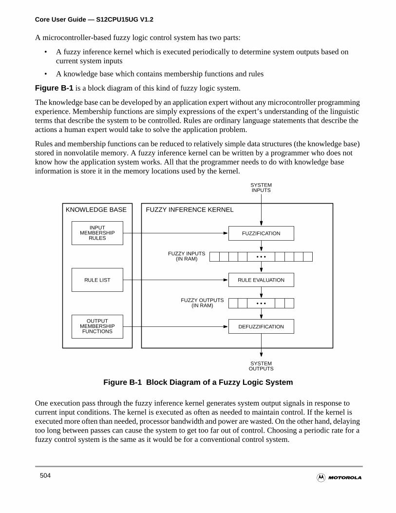
Core User Guide — S12CPU15UG V1.2
on
mingguisticcribe the
e base) note
se toel is
delayingte for a
A microcontroller-based fuzzy logic control system has two parts:
• A fuzzy inference kernel which is executed periodically to determine system outputs based current system inputs
• A knowledge base which contains membership functions and rules
Figure B-1 is a block diagram of this kind of fuzzy logic system.
The knowledge base can be developed by an application expert without any microcontroller programexperience. Membership functions are simply expressions of the expert’s understanding of the linterms that describe the system to be controlled. Rules are ordinary language statements that desactions a human expert would take to solve the application problem.
Rules and membership functions can be reduced to relatively simple data structures (the knowledgstored in nonvolatile memory. A fuzzy inference kernel can be written by a programmer who doesknow how the application system works. All that the programmer needs to do with knowledge basinformation is store it in the memory locations used by the kernel.
Figure B-1 Block Diagram of a Fuzzy Logic System
One execution pass through the fuzzy inference kernel generates system output signals in responcurrent input conditions. The kernel is executed as often as needed to maintain control. If the kernexecuted more often than needed, processor bandwidth and power are wasted. On the other hand,too long between passes can cause the system to get too far out of control. Choosing a periodic rafuzzy control system is the same as it would be for a conventional control system.
INPUT
RULE LIST
OUTPUT
FUZZIFICATION
RULE EVALUATION
DEFUZZIFICATION
KNOWLEDGE BASE
SYSTEM
SYSTEM
FUZZY INPUTS
FUZZY OUTPUTS
• • •
MEMBERSHIPRULES
MEMBERSHIPFUNCTIONS
FUZZY INFERENCE KERNEL
• • •(IN RAM)
(IN RAM)
OUTPUTS
INPUTS
504
Core User Guide — S12CPU15UG V1.2
ershipplishedbel oft. To
sually
input.input.
TheFF orree to
nd istion
indexexMoint toxceptystem
itions.
B.3.1 Fuzzification (MEM)
During the fuzzification step, the current system input values are compared to stored input membfunctions to determine the degree to which each label of each system input is true. This is accomby finding the y-value for the current input value on a trapezoidal membership function for each laeach system input. The MEM instruction performs this calculation for one label of one system inpuperform the complete fuzzification task for a system, several MEM instructions must be executed, uin a program loop structure.
Figure B-2 shows a system of three input membership functions, one for each label of the systemThe x-axis of all three membership functions represents the range of possible values of the systemThe vertical line through all three membership functions represents a specific system input value.y-axis represents degree of truth and varies from completely false ($00 or 0%) to completely true ($100%). The y-value where the vertical line intersects each of the membership functions is the degwhich the current input value matches the associated label for this system input. For example, theexpression “temperature is warm” is 25% true ($40). The value $40 is stored to a RAM location, acalled a fuzzy input (in this case, the fuzzy input for “the temperature is warm”). There is a RAM locafor each fuzzy input (for each label of each system input).
When the fuzzification step begins, the current value of the system input is in an accumulator, oneregister points to the first membership function definition in the knowledge base, and a second indregister points to the first fuzzy input in RAM. As each fuzzy input is calculated by executing a MEinstruction, the result is stored to the fuzzy input and both pointers are updated automatically to pthe locations associated with the next fuzzy input. The MEM instruction takes care of everything ecounting the number of labels per system input and loading the current value of any subsequent sinputs.
The end result of the fuzzification step is a table of fuzzy inputs representing current system cond
505
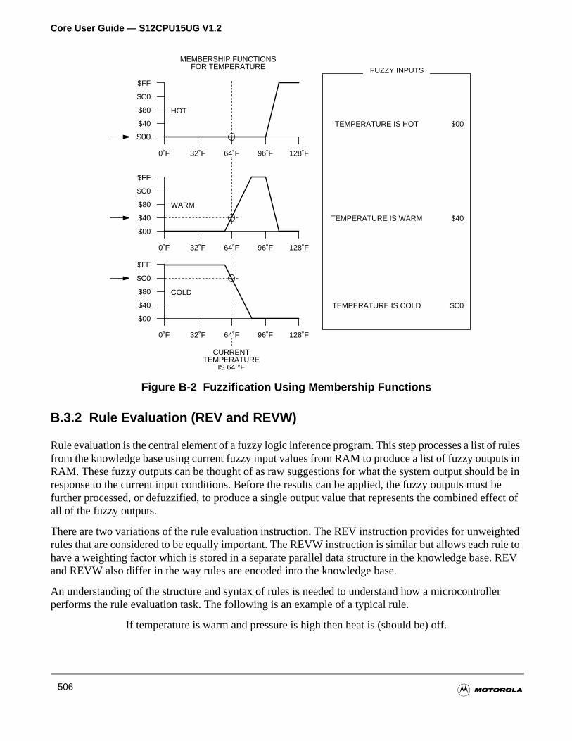
Core User Guide — S12CPU15UG V1.2
f rulests inbe in
t beffect of
htedule toe. REV
ller
Figure B-2 Fuzzification Using Membership Functions
B.3.2 Rule Evaluation (REV and REVW)
Rule evaluation is the central element of a fuzzy logic inference program. This step processes a list ofrom the knowledge base using current fuzzy input values from RAM to produce a list of fuzzy outpuRAM. These fuzzy outputs can be thought of as raw suggestions for what the system output shouldresponse to the current input conditions. Before the results can be applied, the fuzzy outputs musfurther processed, or defuzzified, to produce a single output value that represents the combined eall of the fuzzy outputs.
There are two variations of the rule evaluation instruction. The REV instruction provides for unweigrules that are considered to be equally important. The REVW instruction is similar but allows each rhave a weighting factor which is stored in a separate parallel data structure in the knowledge basand REVW also differ in the way rules are encoded into the knowledge base.
An understanding of the structure and syntax of rules is needed to understand how a microcontroperforms the rule evaluation task. The following is an example of a typical rule.
If temperature is warm and pressure is high then heat is (should be) off.
$00
$80
$FF
0˚F 32˚F 64˚F 96˚F 128˚F
$40
$C0
HOT
$00
$80
$FF
0˚F 32˚F 64˚F 96˚F 128˚F
$40
$C0
WARM
$00
$80
$FF
0˚F 32˚F 64˚F 96˚F 128˚F
$40
$C0
COLD
CURRENT
MEMBERSHIP FUNCTIONS
FUZZY INPUTS
TEMPERATURE IS HOT
TEMPERATURE IS WARM
TEMPERATURE IS COLD
$00
$40
$C0
FOR TEMPERATURE
TEMPERATUREIS 64 °F
506

Core User Guide — S12CPU15UG V1.2
troller leftutput
fuzzy
ch
. Thech they
uent
n be
uts andhich
when
ts andend ofquents.rved
umber ofbility of
ted
zyeaningll truththect theles are
t rule by a
hen
valuesledge
At first glance, it seems that encoding this rule in a compact form understandable to the microconwould be difficult, but it is actually simple to reduce the rule to a small list of memory pointers. Theportion of the rule is a statement of input conditions and the right portion of the rule is a statement of oactions.
The left portion of a rule is made up of one or more (in this case two) antecedents connected by aandoperator. Each antecedent expression consists of the name of a system input, followed byis, followedby a label name. The label must be defined by a membership function in the knowledge base. Eaantecedent expression corresponds to one of the fuzzy inputs in RAM. Sinceand is the only operatorallowed to connect antecedent expressions, there is no need to include these in the encoded ruleantecedents can be encoded as a simple list of pointers to (or addresses of) the fuzzy inputs to whirefer.
The right portion of a rule is made up of one or more (in this case one) consequents. Each conseqexpression consists of the name of a system output, followed byis, followed by a label name. Eachconsequent expression corresponds to a specific fuzzy output in RAM. Consequents for a rule caencoded as a simple list of pointers to (or addresses of) the fuzzy outputs to which they refer.
The complete rules are stored in the knowledge base as a list of pointers or addresses of fuzzy inpfuzzy outputs. In order for the rule evaluation logic to work, there must be some means of knowing wpointers refer to fuzzy inputs, and which refer to fuzzy outputs. There also must be a way to knowthe last rule in the system has been reached.
One method of organization is to have a fixed number of rules with a specific number of antecedenconsequents. A second method, employed in Motorola Freeware M68HC11 kernels, is to mark thethe rule list with a reserved value, and use a bit in the pointers to distinguish antecedents from conseA third method of organization, used in the HCS12 CPU, is to mark the end of the rule list with a resevalue, and separate antecedents and consequents with another reserved value. This permits any nrules, and allows each rule to have any number of antecedents and consequents, subject to availasystem memory.
Each rule is evaluated sequentially, but the rules as a group are treated as if they were all evaluasimultaneously. Two mathematical operations take place during rule evaluation. The fuzzyand operatorcorresponds to the mathematical minimum operation and the fuzzyor operation corresponds to themathematical maximum operation. The fuzzyandis used to connect antecedents within a rule. The fuzor is implied between successive rules. Before evaluating any rules, all fuzzy outputs are cleared, mnot true at all. As each rule is evaluated, the smallest (minimum) antecedent is taken to be the overaof the rule. This rule truth value is applied to each consequent of the rule (by storing this value to corresponding fuzzy output) unless the fuzzy output is already larger (maximum). If two rules affesame fuzzy output, the rule that is most true governs the value in the fuzzy output because the ruconnected by an implied fuzzyor.
In the case of rule weighting, the truth value for a rule is determined as usual by finding the smallesantecedent. Before applying this truth value to the consequents for the rule, the value is multipliedfraction from zero (rule disabled) to one (rule fully enabled). The resulting modified truth value is tapplied to the fuzzy outputs.
The end result of the rule evaluation step is a table of suggested or raw fuzzy outputs in RAM. Thesewere obtained by plugging current conditions (fuzzy input values) into the system rules in the know
507
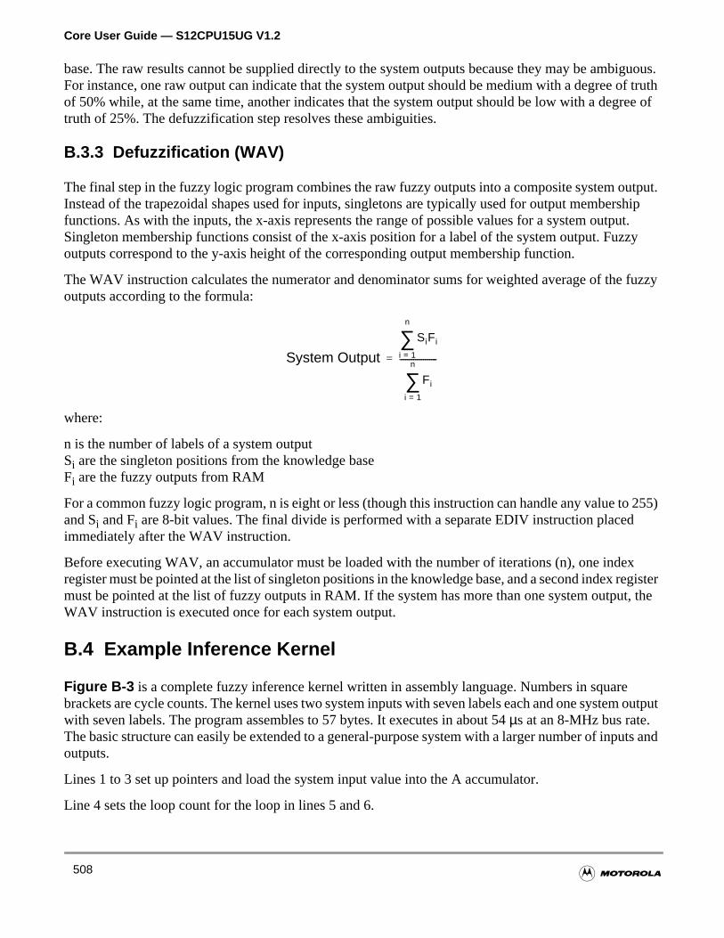
Core User Guide — S12CPU15UG V1.2
biguous.f truthree of
utput.shiput.zy
fuzzy
255)
xegistert, the
output
uts and
base. The raw results cannot be supplied directly to the system outputs because they may be amFor instance, one raw output can indicate that the system output should be medium with a degree oof 50% while, at the same time, another indicates that the system output should be low with a degtruth of 25%. The defuzzification step resolves these ambiguities.
B.3.3 Defuzzification (WAV)
The final step in the fuzzy logic program combines the raw fuzzy outputs into a composite system oInstead of the trapezoidal shapes used for inputs, singletons are typically used for output memberfunctions. As with the inputs, the x-axis represents the range of possible values for a system outpSingleton membership functions consist of the x-axis position for a label of the system output. Fuzoutputs correspond to the y-axis height of the corresponding output membership function.
The WAV instruction calculates the numerator and denominator sums for weighted average of theoutputs according to the formula:
where:
n is the number of labels of a system outputSi are the singleton positions from the knowledge baseFi are the fuzzy outputs from RAM
For a common fuzzy logic program, n is eight or less (though this instruction can handle any value toand Si and Fi are 8-bit values. The final divide is performed with a separate EDIV instruction placedimmediately after the WAV instruction.
Before executing WAV, an accumulator must be loaded with the number of iterations (n), one inderegister must be pointed at the list of singleton positions in the knowledge base, and a second index rmust be pointed at the list of fuzzy outputs in RAM. If the system has more than one system outpuWAV instruction is executed once for each system output.
B.4 Example Inference Kernel
Figure B-3 is a complete fuzzy inference kernel written in assembly language. Numbers in squarebrackets are cycle counts. The kernel uses two system inputs with seven labels each and one systemwith seven labels. The program assembles to 57 bytes. It executes in about 54µs at an 8-MHz bus rate.The basic structure can easily be extended to a general-purpose system with a larger number of inpoutputs.
Lines 1 to 3 set up pointers and load the system input value into the A accumulator.
Line 4 sets the loop count for the loop in lines 5 and 6.
System Output
SiFi
i 1=
n
∑
Fi
i 1=
n
∑-------------------=
508
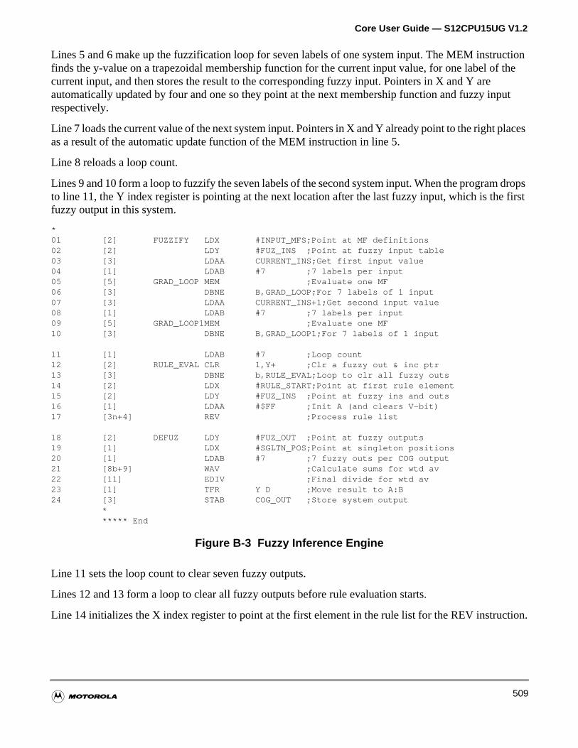
Core User Guide — S12CPU15UG V1.2
ction the
put
laces
drops first
ion.
Lines 5 and 6 make up the fuzzification loop for seven labels of one system input. The MEM instrufinds the y-value on a trapezoidal membership function for the current input value, for one label ofcurrent input, and then stores the result to the corresponding fuzzy input. Pointers in X and Y areautomatically updated by four and one so they point at the next membership function and fuzzy inrespectively.
Line 7 loads the current value of the next system input. Pointers in X and Y already point to the right pas a result of the automatic update function of the MEM instruction in line 5.
Line 8 reloads a loop count.
Lines 9 and 10 form a loop to fuzzify the seven labels of the second system input. When the programto line 11, the Y index register is pointing at the next location after the last fuzzy input, which is thefuzzy output in this system.
*01 [2] FUZZIFY LDX #INPUT_MFS;Point at MF definitions02 [2] LDY #FUZ_INS ;Point at fuzzy input table03 [3] LDAA CURRENT_INS;Get first input value04 [1] LDAB #7 ;7 labels per input05 [5] GRAD_LOOP MEM ;Evaluate one MF06 [3] DBNE B,GRAD_LOOP;For 7 labels of 1 input07 [3] LDAA CURRENT_INS+1;Get second input value08 [1] LDAB #7 ;7 labels per input09 [5] GRAD_LOOP1MEM ;Evaluate one MF10 [3] DBNE B,GRAD_LOOP1;For 7 labels of 1 input
11 [1] LDAB #7 ;Loop count12 [2] RULE_EVAL CLR 1,Y+ ;Clr a fuzzy out & inc ptr13 [3] DBNE b,RULE_EVAL;Loop to clr all fuzzy outs14 [2] LDX #RULE_START;Point at first rule element15 [2] LDY #FUZ_INS ;Point at fuzzy ins and outs16 [1] LDAA #$FF ;Init A (and clears V-bit)17 [3n+4] REV ;Process rule list
18 [2] DEFUZ LDY #FUZ_OUT ;Point at fuzzy outputs19 [1] LDX #SGLTN_POS;Point at singleton positions20 [1] LDAB #7 ;7 fuzzy outs per COG output21 [8b+9] WAV ;Calculate sums for wtd av22 [11] EDIV ;Final divide for wtd av23 [1] TFR Y D ;Move result to A:B24 [3] STAB COG_OUT ;Store system output
****** End
Figure B-3 Fuzzy Inference Engine
Line 11 sets the loop count to clear seven fuzzy outputs.
Lines 12 and 13 form a loop to clear all fuzzy outputs before rule evaluation starts.
Line 14 initializes the X index register to point at the first element in the rule list for the REV instruct
509
Core User Guide — S12CPU15UG V1.2
e list. The.
uzzydition, the Ving
t untilch, they.
a
tionsto use
onns.
d tosor and and
e
tions.
Line 15 initializes the Y index register to point at the fuzzy inputs and outputs in the system. The rul(for REV) consists of 8-bit offsets from this base address to particular fuzzy inputs or fuzzy outputsspecial value $FE is interpreted by REV as a marker between rule antecedents and consequents
Line 16 initializes the A accumulator to the highest 8-bit value in preparation for finding the smallest finput referenced by a rule antecedent. The LDAA #$FF instruction also clears the V bit in the concode register so the REV instruction knows it is processing antecedents. During rule list processingbit is toggled each time an $FE is detected in the list. The V bit indicates whether REV is processantecedents or consequents.
Line 17 is the REV instruction, a self-contained loop to process successive elements in the rule lisan $FF character is found. For a system of 17 rules with two antecedents and one consequent eaREV instruction takes 259 cycles, but it is interruptible so it does not cause a long interrupt latenc
Lines 18 through 20 set up pointers and an iteration count for the WAV instruction.
Line 21 is the beginning of defuzzification. The WAV instruction calculates a sum-of-products andsum-of-weights.
Line 22 completes defuzzification. The EDIV instruction performs a 32-bit by 16-bit divide on theintermediate results from WAV to get the weighted average.
Line 23 moves the EDIV result into the double accumulator.
Line 24 stores the low 8-bits of the defuzzification result.
This example inference program shows how easy it is to incorporate fuzzy logic into general applicausing the HCS12 CPU. Code space and execution time are no longer serious factors in the decisionfuzzy logic. The next section begins a much more detailed look at the fuzzy logic instructions.
B.5 MEM Instruction Details
This section provides a more detailed explanation of the membership function evaluation instructi(MEM), including details about abnormal special cases for improperly defined membership functio
B.5.1 Membership Function Definitions
Figure B-4 shows how a normal membership function is specified. Typically a software tool is useinput membership functions graphically, and the tool generates data structures for the target processoftware kernel. Alternatively, points and slopes for the membership functions can be determinedstored in memory with define-constant assembler directives.
An internal CPU algorithm calculates the y-value where the current input intersects a membershipfunction. This algorithm assumes the membership function obeys some common-sense rules. If thmembership function definition is improper, the results may be unusual.B.5.2 Abnormal MembershipFunction Definitions discusses these cases. The following rules apply to normal membership func
• $00≤ point1< $FF
• $00< point2≤ $FF
510
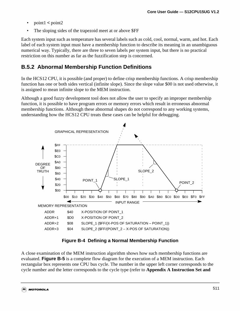
Core User Guide — S12CPU15UG V1.2
ot. Eachiguousl
rshipise, it
hipals,
to the
• point1< point2
• The sloping sides of the trapezoid meet at or above $FF
Each system input such as temperature has several labels such as cold, cool, normal, warm, and hlabel of each system input must have a membership function to describe its meaning in an unambnumerical way. Typically, there are three to seven labels per system input, but there is no practicarestriction on this number as far as the fuzzification step is concerned.
B.5.2 Abnormal Membership Function Definitions
In the HCS12 CPU, it is possible (and proper) to define crisp membership functions. A crisp membefunction has one or both sides vertical (infinite slope). Since the slope value $00 is not used otherwis assigned to mean infinite slope to the MEM instruction.
Although a good fuzzy development tool does not allow the user to specify an improper membersfunction, it is possible to have program errors or memory errors which result in erroneous abnormmembership functions. Although these abnormal shapes do not correspond to any working systemunderstanding how the HCS12 CPU treats these cases can be helpful for debugging.
Figure B-4 Defining a Normal Membership Function
A close examination of the MEM instruction algorithm shows how such membership functions areevaluated.Figure B-5 is a complete flow diagram for the execution of a MEM instruction. Eachrectangular box represents one CPU bus cycle. The number in the upper left corner corresponds cycle number and the letter corresponds to the cycle type (refer toAppendix A Instruction Set and
GRAPHICAL REPRESENTATION
$00 $10 $20 $30 $40 $50 $60 $70 $80 $90 $A0 $B0 $C0 $D0 $E0 $F0 $FF
$00
$20
$40
$60
$80
$A0
$FF
$E0
$C0
MEMORY REPRESENTATION
ADDR
ADDR+1
ADDR+2
ADDR+3
$40
$D0
$08
$04
X-POSITION OF POINT_1
X-POSITION OF POINT_2
SLOPE_1 ($FF/(X-POS OF SATURATION – POINT_1))
SLOPE_2 ($FF/(POINT_2 – X-POS OF SATURATION))
POINT_1POINT_2
SLOPE_1
SLOPE_2
DEGREEOF
TRUTH
INPUT RANGE
511
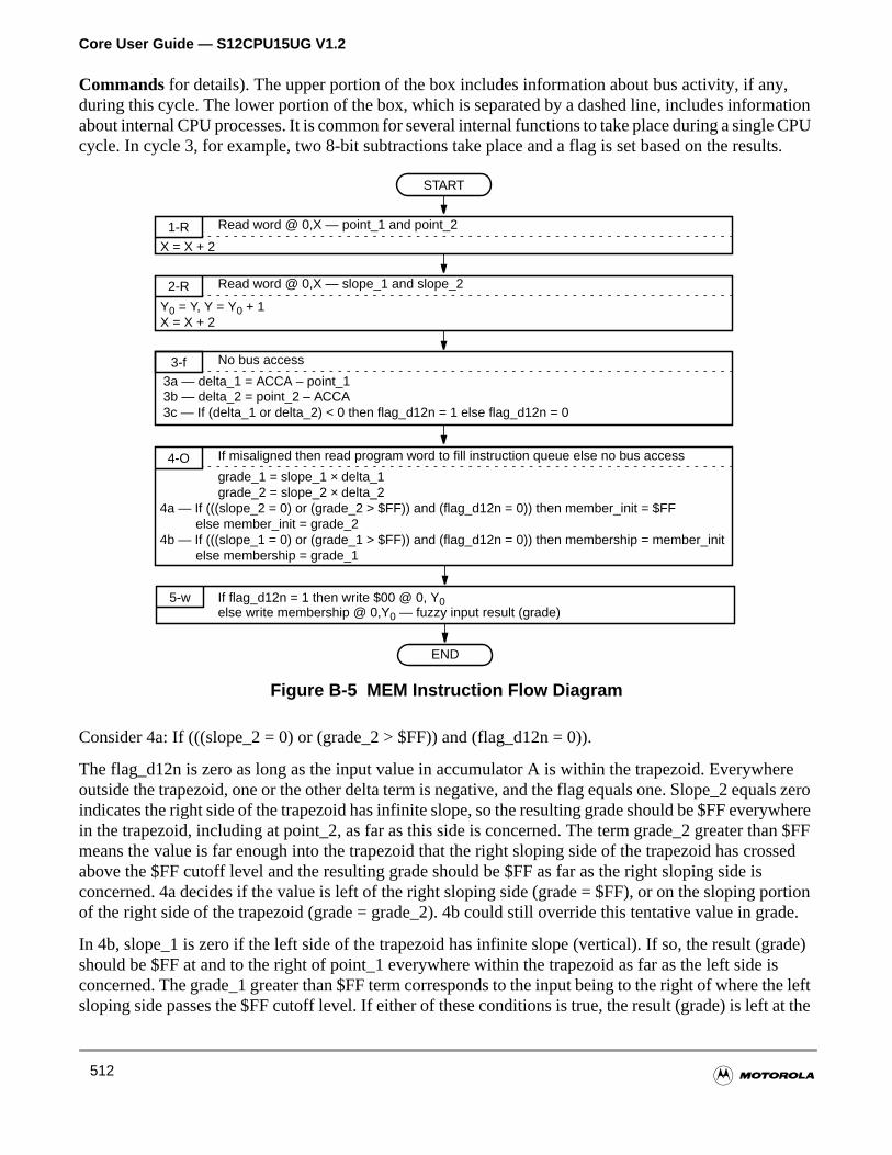
Core User Guide — S12CPU15UG V1.2
,atione CPUlts.
ereals zerowhere
an $FFossed
ortionade.
rade) isthe leftat the
Commands for details). The upper portion of the box includes information about bus activity, if anyduring this cycle. The lower portion of the box, which is separated by a dashed line, includes informabout internal CPU processes. It is common for several internal functions to take place during a singlcycle. In cycle 3, for example, two 8-bit subtractions take place and a flag is set based on the resu
Figure B-5 MEM Instruction Flow Diagram
Consider 4a: If (((slope_2 = 0) or (grade_2 > $FF)) and (flag_d12n = 0)).
The flag_d12n is zero as long as the input value in accumulator A is within the trapezoid. Everywhoutside the trapezoid, one or the other delta term is negative, and the flag equals one. Slope_2 equindicates the right side of the trapezoid has infinite slope, so the resulting grade should be $FF everyin the trapezoid, including at point_2, as far as this side is concerned. The term grade_2 greater thmeans the value is far enough into the trapezoid that the right sloping side of the trapezoid has crabove the $FF cutoff level and the resulting grade should be $FF as far as the right sloping side isconcerned. 4a decides if the value is left of the right sloping side (grade = $FF), or on the sloping pof the right side of the trapezoid (grade = grade_2). 4b could still override this tentative value in gr
In 4b, slope_1 is zero if the left side of the trapezoid has infinite slope (vertical). If so, the result (gshould be $FF at and to the right of point_1 everywhere within the trapezoid as far as the left sideconcerned. The grade_1 greater than $FF term corresponds to the input being to the right of wheresloping side passes the $FF cutoff level. If either of these conditions is true, the result (grade) is left
1-R Read word @ 0,X — point_1 and point_2
2-R Read word @ 0,X — slope_1 and slope_2
3a — delta_1 = ACCA – point_13b — delta_2 = point_2 – ACCA3c — If (delta_1 or delta_2) < 0 then flag_d12n = 1 else flag_d12n = 0
4-O If misaligned then read program word to fill instruction queue else no bus access
4a — If (((slope_2 = 0) or (grade_2 > $FF)) and (flag_d12n = 0)) then member_init = $FFelse member_init = grade_2
4b — If (((slope_1 = 0) or (grade_1 > $FF)) and (flag_d12n = 0)) then membership = member_initelse membership = grade_1
START
END
X = X + 2
grade_1 = slope_1 × delta_1grade_2 = slope_2 × delta_2
Y0 = Y, Y = Y0 + 1X = X + 2
3-f
If flag_d12n = 1 then write $00 @ 0, Y0
No bus access
5-welse write membership @ 0,Y0 — fuzzy input result (grade)
512
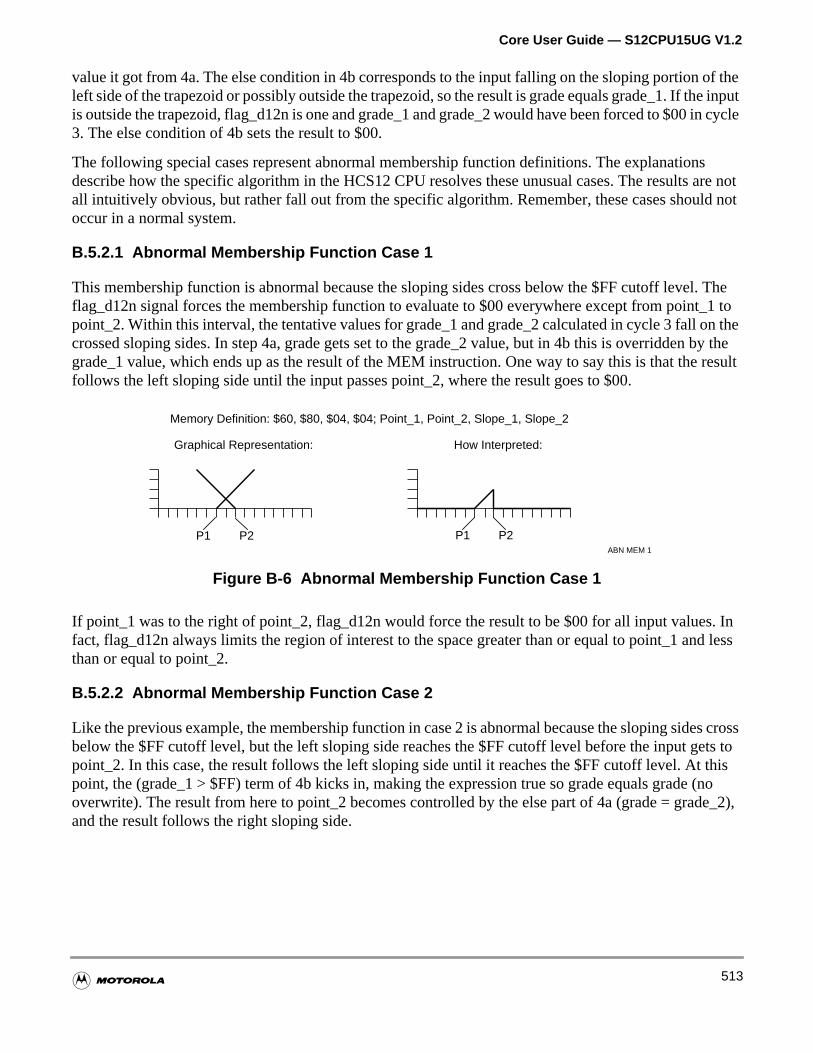
Core User Guide — S12CPU15UG V1.2
f thee inputin cycle
s are notld not
l. Thet_1 ton the by the result
s. Ind less
s crossets tothis (node_2),
value it got from 4a. The else condition in 4b corresponds to the input falling on the sloping portion oleft side of the trapezoid or possibly outside the trapezoid, so the result is grade equals grade_1. If this outside the trapezoid, flag_d12n is one and grade_1 and grade_2 would have been forced to $003. The else condition of 4b sets the result to $00.
The following special cases represent abnormal membership function definitions. The explanationdescribe how the specific algorithm in the HCS12 CPU resolves these unusual cases. The resultsall intuitively obvious, but rather fall out from the specific algorithm. Remember, these cases shouoccur in a normal system.
B.5.2.1 Abnormal Membership Function Case 1
This membership function is abnormal because the sloping sides cross below the $FF cutoff leveflag_d12n signal forces the membership function to evaluate to $00 everywhere except from poinpoint_2. Within this interval, the tentative values for grade_1 and grade_2 calculated in cycle 3 fall ocrossed sloping sides. In step 4a, grade gets set to the grade_2 value, but in 4b this is overriddengrade_1 value, which ends up as the result of the MEM instruction. One way to say this is that thefollows the left sloping side until the input passes point_2, where the result goes to $00.
Figure B-6 Abnormal Membership Function Case 1
If point_1 was to the right of point_2, flag_d12n would force the result to be $00 for all input valuefact, flag_d12n always limits the region of interest to the space greater than or equal to point_1 anthan or equal to point_2.
B.5.2.2 Abnormal Membership Function Case 2
Like the previous example, the membership function in case 2 is abnormal because the sloping sidebelow the $FF cutoff level, but the left sloping side reaches the $FF cutoff level before the input gpoint_2. In this case, the result follows the left sloping side until it reaches the $FF cutoff level. At point, the (grade_1 > $FF) term of 4b kicks in, making the expression true so grade equals gradeoverwrite). The result from here to point_2 becomes controlled by the else part of 4a (grade = graand the result follows the right sloping side.
Memory Definition: $60, $80, $04, $04; Point_1, Point_2, Slope_1, Slope_2
Graphical Representation: How Interpreted:
P1 P2 P1 P2ABN MEM 1
513
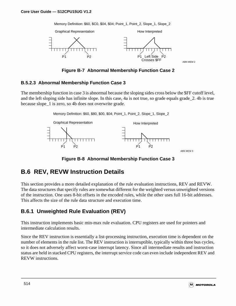
Core User Guide — S12CPU15UG V1.2
ff level,b is true
VW.ersionsesses.
d
on theles,ructionEV and
Figure B-7 Abnormal Membership Function Case 2
B.5.2.3 Abnormal Membership Function Case 3
The membership function in case 3 is abnormal because the sloping sides cross below the $FF cutoand the left sloping side has infinite slope. In this case, 4a is not true, so grade equals grade_2. 4because slope_1 is zero, so 4b does not overwrite grade.
Figure B-8 Abnormal Membership Function Case 3
B.6 REV, REVW Instruction Details
This section provides a more detailed explanation of the rule evaluation instructions, REV and REThe data structures that specify rules are somewhat different for the weighted versus unweighted vof the instruction. One uses 8-bit offsets in the encoded rules, while the other uses full 16-bit addrThis affects the size of the rule data structure and execution time.
B.6.1 Unweighted Rule Evaluation (REV)
This instruction implements basic min-max rule evaluation. CPU registers are used for pointers anintermediate calculation results.
Since the REV instruction is essentially a list-processing instruction, execution time is dependent number of elements in the rule list. The REV instruction is interruptible, typically within three bus cycso it does not adversely affect worst-case interrupt latency. Since all intermediate results and inststatus are held in stacked CPU registers, the interrupt service code can even include independent RREVW instructions.
Memory Definition: $60, $C0, $04, $04; Point_1, Point_2, Slope_1, Slope_2
Graphical Representation How Interpreted
P1 P2 P1 P2Left SideCrosses $FF
ABN MEM 2
Memory Definition: $60, $80, $00, $04; Point_1, Point_2, Slope_1, Slope_2
Graphical Representation How Interpreted
P1 P2 P1 P2ABN MEM 3
514
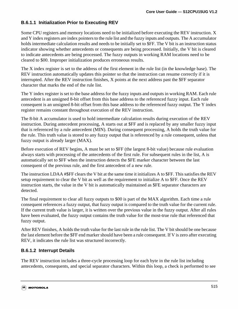
Core User Guide — S12CPU15UG V1.2
ion. Xulator
statuscleared be
). The isr
h ruleruleindex
Vinput
lue forss that
ationA is
EVVre
lent rule.lesed that
auseecuting
ed to see
B.6.1.1 Initialization Prior to Executing REV
Some CPU registers and memory locations need to be initialized before executing the REV instructand Y index registers are index pointers to the rule list and the fuzzy inputs and outputs. The A accumholds intermediate calculation results and needs to be initially set to $FF. The V bit is an instructionindicator showing whether antecedents or consequents are being processed. Initially, the V bit is to indicate antecedents are being processed. The fuzzy outputs in working RAM locations need tocleared to $00. Improper initialization produces erroneous results.
The X index register is set to the address of the first element in the rule list (in the knowledge baseREV instruction automatically updates this pointer so that the instruction can resume correctly if itinterrupted. After the REV instruction finishes, X points at the next address past the $FF separatocharacter that marks the end of the rule list.
The Y index register is set to the base address for the fuzzy inputs and outputs in working RAM. Eacantecedent is an unsigned 8-bit offset from this base address to the referenced fuzzy input. Each consequent is an unsigned 8-bit offset from this base address to the referenced fuzzy output. The Yregister remains constant throughout execution of the REV instruction.
The 8-bit A accumulator is used to hold intermediate calculation results during execution of the REinstruction. During antecedent processing, A starts out at $FF and is replaced by any smaller fuzzythat is referenced by a rule antecedent (MIN). During consequent processing, A holds the truth vathe rule. This truth value is stored to any fuzzy output that is referenced by a rule consequent, unlefuzzy output is already larger (MAX).
Before execution of REV begins, A must be set to $FF (the largest 8-bit value) because rule evalualways starts with processing of the antecedents of the first rule. For subsequent rules in the list, automatically set to $FF when the instruction detects the $FE marker character between the lastconsequent of the previous rule, and the first antecedent of a new rule.
The instruction LDAA #$FF clears the V bit at the same time it initializes A to $FF. This satisfies the Rsetup requirement to clear the V bit as well as the requirement to initialize A to $FF. Once the REinstruction starts, the value in the V bit is automatically maintained as $FE separator characters adetected.
The final requirement to clear all fuzzy outputs to $00 is part of the MAX algorithm. Each time a ruconsequent references a fuzzy output, that fuzzy output is compared to the truth value for the curreIf the current truth value is larger, it is written over the previous value in the fuzzy output. After all ruhave been evaluated, the fuzzy output contains the truth value for the most-true rule that referencfuzzy output.
After REV finishes, A holds the truth value for the last rule in the rule list. The V bit should be one becthe last element before the $FF end marker should have been a rule consequent. If V is zero after exREV, it indicates the rule list was structured incorrectly.
B.6.1.2 Interrupt Details
The REV instruction includes a three-cycle processing loop for each byte in the rule list includingantecedents, consequents, and special separator characters. Within this loop, a check is perform
515
Core User Guide — S12CPU15UG V1.2
reausesd not
e REVV
tionration
in theand ave CPU
nrner of
d takes
place.vesointction.pe ofwhichole value.
Vile the part of
if any qualified interrupt request is pending. If an interrupt is detected, the current CPU registers astacked and the interrupt is serviced. When the interrupt service routine finishes, an RTI instruction cthe CPU to recover its previous context from the stack, and the REV instruction is resumed as if it habeen interrupted.
When a REV instruction is interrupted, the stacked value of the program counter, PC, points to thinstruction rather than the instruction that follows. This causes the CPU to try to execute a new REinstruction upon return from the interrupt. Since the CPU registers, including the V bit in the condicode register, indicate the current status of the interrupted REV instruction, the rule evaluation operesumes where it was interrupted.
B.6.1.3 Cycle-by-Cycle REV Details
The central element of the REV instruction is a three-cycle loop that is executed once for each byterule list. There is a small amount of housekeeping activity to get this loop started as REV begins, small sequence to end the instruction. If an interrupt comes, there is a special small sequence to sastatus on the stack before servicing the requested interrupt.
Figure B-9 is a REV instruction flow diagram. Each box represents one CPU clock cycle. Decisioblocks and connecting arrows are considered to take no time at all. The letters in the upper left coeach box are execution cycle codes (refer toAppendix A Instruction Set and Commands for details).
When a value is read from memory, it cannot be used by the CPU until the second cycle after the reaplace. This is due to access and propagation delays.
Since there is more than one flow path through the REV instruction, cycle numbers have a decimalThis decimal place indicates which of several possible paths is being used. The CPU normally moforward by one digit at a time within the same flow. The flow number is indicated after the decimal pin the cycle number. There are two exceptions possible to this orderly sequence through an instruThe first is a branch back to an earlier cycle number to form a loop as in 6.0 to 4.0. The second tysequence change is from one flow to a parallel flow within the same instruction such as 4.0 to 5.2,occurs if the REV instruction senses an interrupt. In this second type of sequence branch, the whnumber advances by one and the flow number, the digit after the decimal point, changes to a new
In cycle 1.0, the CPU does an optional program word access to replace the $18 prebyte of the REinstruction. Notice that cycle 7.0 is also an O cycle. One of these cycles is a program word fetch, whother is a free cycle in which the CPU does not access the bus. Although the $18 page prebyte isthe REV instruction, the CPU treats it as a separate single-cycle instruction.
516
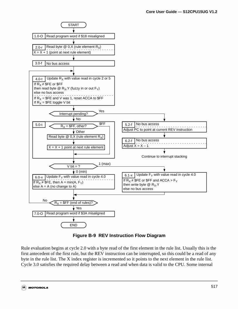
Core User Guide — S12CPU15UG V1.2
s thef any
list.ternal
Figure B-9 REV Instruction Flow Diagram
Rule evaluation begins at cycle 2.0 with a byte read of the first element in the rule list. Usually this ifirst antecedent of the first rule, but the REV instruction can be interrupted, so this could be a read obyte in the rule list. The X index register is incremented so it points to the next element in the ruleCycle 3.0 satisfies the required delay between a read and when data is valid to the CPU. Some in
Interrupt pending?
1.0-O Read program word if $18 misaligned
2.0-r Read byte @ 0,X (rule element RX)
X = X + 1 (point at next rule element)
START
END
4.0-t
then read byte @ RX,Y (fuzzy in or out FY)If RX ≠ $FE or $FF
No
Yes
Continue to interrupt stacking
Yes
No
3.0-f No bus access
If RX = $FE and V was 1, reset ACCA to $FFIf RX = $FE toggle V bit
else no bus access
Update RX with value read in cycle 2 or 5
RX = $FF (end of rules)?
5.0-t RX = $FF, other?$FF
OtherRead byte @ 0,X (rule element RX)
X = X + 1 point at next rule element
V bit = ?1 (max)
0 (min)
6.0-x Update FY with value read in cycle 4.0
If RX ≠ $FE, then A = min(A, FY)else A = A (no change to A)
7.0-O Read program word if $3A misaligned
5.2-f No bus access
Adjust PC to point at current REV instruction
6.2-f No bus access
Adjust X = X – 1
6.1-x
then write byte @ RX,YIf RX ≠ $FE or $FF and ACCA > FY
else no bus access
Update FY with value read in cycle 4.0
517
Core User Guide — S12CPU15UG V1.2
e rule
4.0, 5.0,e $FF
ith theuses the
offset
ts of thefinds to
nts ared and the
input
lthough
d 5.0les 5.2n cycle, rulee thee the
s areruleresult
CPU housekeeping activity takes place during this cycle, but there is no bus activity. By cycle 4.0, thelement that was read in cycle 2.0 is available to the CPU.
Cycle 4.0 is the first cycle of the main three-cycle rule evaluation loop. Depending on whether ruleantecedents or consequents are being processed, the loop consists of cycles 4.0, 5.0, and 6.0 or and 6.1. This loop is executed once for every byte in the rule list, including the $FE separators and thend-of-rules marker.
At each cycle 4.0, a fuzzy input or fuzzy output is read, except during the loop passes associated w$FE and $FF marker bytes, in which no bus access takes place during cycle 4.0. The read accessY index register as the base address and the previously read rule byte, RX, as an unsigned offset from Y.The fuzzy input or output value read here is used during the next cycle 6.0 or 6.1. Besides being thefrom Y for this read, the previously read RX can be a separator character, $FE. If RX is $FE and the V bitwas one, this indicates a switch from processing consequents of one rule to processing antecedennext rule. At this transition, the A accumulator is initialized to $FF to prepare for the min operation tothe smallest fuzzy input. Also, if RX is $FE, the V bit toggles to indicate the change from antecedentconsequents, or consequents to antecedents.
During cycle 5.0, a new rule byte is read unless this is the last loop pass, and RX is $FF, marking the endof the rule list. This new rule byte is not used until cycle 4.0 of the next pass through the loop.
Between cycle 5.0 and 6.x, the V bit determines which of two paths to take. If V is zero, antecedebeing processed and the CPU progresses to cycle 6.0. If V is one, consequents are being processeCPU goes to cycle 6.1.
During cycle 6.0, the min operation compares the current value in the A accumulator to the fuzzy that was read in the previous cycle 4.0 and puts the lower value in the A accumulator. If RX is $FE, this isthe transition between rule antecedents and rule consequents, and the min operation is skipped athe cycle is still used. Cycle 6.0/6.1 is an x cycle because it could be a byte write or a free cycle.
If an interrupt arrives while the REV instruction is executing, REV can break between cycles 4.0 anin an orderly fashion so that the rule evaluation operation can resume after the interrupt service. Cycand 6.2 adjust the PC and X index register so the REV operation can recover after the interrupt. I5.2, PC is decremented so that it points to the currently-running REV instruction. After the interruptevaluation resumes, but the stacked values for the index registers, accumulator A, and CCR causoperation to pick up where it left off. In cycle 6.2, the X index register is decremented by one becauslast rule byte needs to be refetched when the REV instruction resumes.
After cycle 6.2, the REV instruction is finished, and execution continues with the normal interruptprocessing flow.
B.6.2 Weighted Rule Evaluation (REVW)
This instruction implements a weighted variation of min-max rule evaluation. The weighting factorstored in a table with one 8-bit entry per rule. The weight is used to multiply the truth value of the (minimum of all antecedents) by a value from zero to one to get the weighted result. This weightedis then applied to the consequents, just as it would be for unweighted rule evaluation.
518
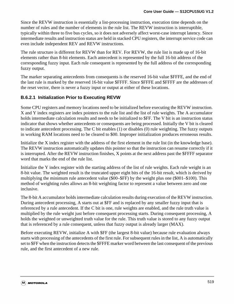
Core User Guide — S12CPU15UG V1.2
the
inceode can
ttheonding
e end ofesses of
ction.latorstatusclearedutputssults.
ase).ly if itarator
is aned byhisone
tion. islue is
sing, Autput
aysticallyrevious
Since the REVW instruction is essentially a list-processing instruction, execution time depends onnumber of rules and the number of elements in the rule list. The REVW instruction is interruptible,typically within three to five bus cycles, so it does not adversely affect worst-case interrupt latency. Sintermediate results and instruction status are held in stacked CPU registers, the interrupt service ceven include independent REV and REVW instructions.
The rule structure is different for REVW than for REV. For REVW, the rule list is made up of 16-bielements rather than 8-bit elements. Each antecedent is represented by the full 16-bit address of corresponding fuzzy input. Each rule consequent is represented by the full address of the correspfuzzy output.
The marker separating antecedents from consequents is the reserved 16-bit value $FFFE, and ththe last rule is marked by the reserved 16-bit value $FFFF. Since $FFFE and $FFFF are the addrthe reset vector, there is never a fuzzy input or output at either of these locations.
B.6.2.1 Initialization Prior to Executing REVW
Some CPU registers and memory locations need to be initialized before executing the REVW instruX and Y index registers are index pointers to the rule list and the list of rule weights. The A accumuholds intermediate calculation results and needs to be initialized to $FF. The V bit is an instructionindicator that shows whether antecedents or consequents are being processed. Initially the V bit isto indicate antecedent processing. The C bit enables (1) or disables (0) rule weighting. The fuzzy oin working RAM locations need to be cleared to $00. Improper initialization produces erroneous re
Initialize the X index register with the address of the first element in the rule list (in the knowledge bThe REVW instruction automatically updates this pointer so that the instruction can resume correctis interrupted. After the REVW instruction finishes, X points at the next address past the $FFFF sepword that marks the end of the rule list.
Initialize the Y index register with the starting address of the list of rule weights. Each rule weight 8-bit value. The weighted result is the truncated upper eight bits of the 16-bit result, which is derivmultiplying the minimum rule antecedent value ($00–$FF) by the weight plus one ($001–$100). Tmethod of weighting rules allows an 8-bit weighting factor to represent a value between zero and inclusive.
The 8-bit A accumulator holds intermediate calculation results during execution of the REVW instrucDuring antecedent processing, A starts out at $FF and is replaced by any smaller fuzzy input thatreferenced by a rule antecedent. If the C bit is one, rule weights are enabled, and the rule truth vamultiplied by the rule weight just before consequent processing starts. During consequent procesholds the weighted or unweighted truth value for the rule. This truth value is stored to any fuzzy othat is referenced by a rule consequent, unless that fuzzy output is already larger (MAX).
Before executing REVW, initialize A with $FF (the largest 8-bit value) because rule evaluation alwstarts with processing of the antecedents of the first rule. For subsequent rules in the list, A is automaset to $FF when the instruction detects the $FFFE marker word between the last consequent of the prule, and the first antecedent of a new rule.
519
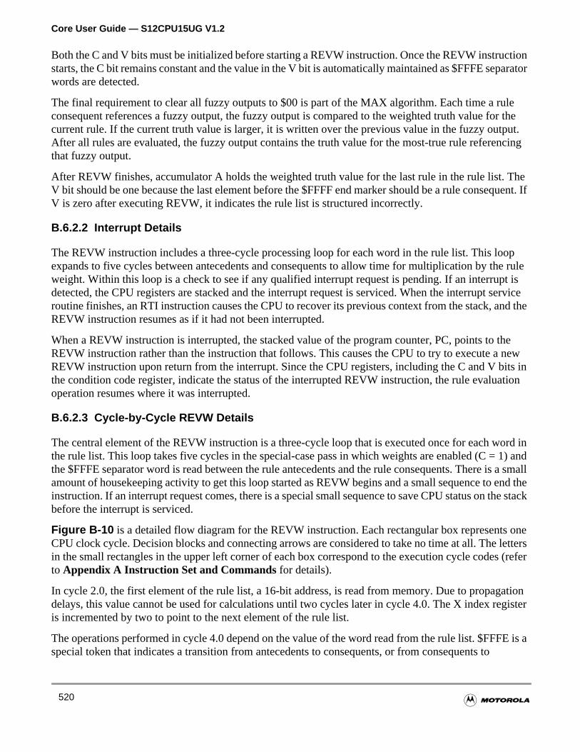
Core User Guide — S12CPU15UG V1.2
tionarator
ler theput.ncing
Theuent. If
ope rulet isservicend the
the newts ination
ord in1) ands a smallnd thee stack
s oneletters(refer
ationgister
E is a
Both the C and V bits must be initialized before starting a REVW instruction. Once the REVW instrucstarts, the C bit remains constant and the value in the V bit is automatically maintained as $FFFE sepwords are detected.
The final requirement to clear all fuzzy outputs to $00 is part of the MAX algorithm. Each time a ruconsequent references a fuzzy output, the fuzzy output is compared to the weighted truth value focurrent rule. If the current truth value is larger, it is written over the previous value in the fuzzy outAfter all rules are evaluated, the fuzzy output contains the truth value for the most-true rule referethat fuzzy output.
After REVW finishes, accumulator A holds the weighted truth value for the last rule in the rule list.V bit should be one because the last element before the $FFFF end marker should be a rule conseqV is zero after executing REVW, it indicates the rule list is structured incorrectly.
B.6.2.2 Interrupt Details
The REVW instruction includes a three-cycle processing loop for each word in the rule list. This loexpands to five cycles between antecedents and consequents to allow time for multiplication by thweight. Within this loop is a check to see if any qualified interrupt request is pending. If an interrupdetected, the CPU registers are stacked and the interrupt request is serviced. When the interrupt routine finishes, an RTI instruction causes the CPU to recover its previous context from the stack, aREVW instruction resumes as if it had not been interrupted.
When a REVW instruction is interrupted, the stacked value of the program counter, PC, points to REVW instruction rather than the instruction that follows. This causes the CPU to try to execute aREVW instruction upon return from the interrupt. Since the CPU registers, including the C and V bithe condition code register, indicate the status of the interrupted REVW instruction, the rule evaluoperation resumes where it was interrupted.
B.6.2.3 Cycle-by-Cycle REVW Details
The central element of the REVW instruction is a three-cycle loop that is executed once for each wthe rule list. This loop takes five cycles in the special-case pass in which weights are enabled (C =the $FFFE separator word is read between the rule antecedents and the rule consequents. There iamount of housekeeping activity to get this loop started as REVW begins and a small sequence to einstruction. If an interrupt request comes, there is a special small sequence to save CPU status on thbefore the interrupt is serviced.
Figure B-10 is a detailed flow diagram for the REVW instruction. Each rectangular box representCPU clock cycle. Decision blocks and connecting arrows are considered to take no time at all. Thein the small rectangles in the upper left corner of each box correspond to the execution cycle codesto Appendix A Instruction Set and Commands for details).
In cycle 2.0, the first element of the rule list, a 16-bit address, is read from memory. Due to propagdelays, this value cannot be used for calculations until two cycles later in cycle 4.0. The X index reis incremented by two to point to the next element of the rule list.
The operations performed in cycle 4.0 depend on the value of the word read from the rule list. $FFFspecial token that indicates a transition from antecedents to consequents, or from consequents to
520
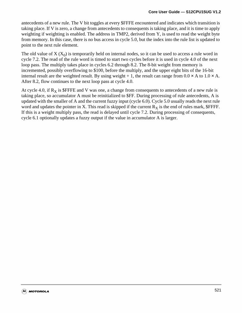
Core User Guide — S12CPU15UG V1.2
ition isapplybyteted to
rd in next
bit
rule iss, A ist rule
nts,
antecedents of a new rule. The V bit toggles at every $FFFE encountered and indicates which transtaking place. If V is zero, a change from antecedents to consequents is taking place, and it is time toweighting if weighting is enabled. The address in TMP2, derived from Y, is used to read the weightfrom memory. In this case, there is no bus access in cycle 5.0, but the index into the rule list is updapoint to the next rule element.
The old value of X (X0) is temporarily held on internal nodes, so it can be used to access a rule wocycle 7.2. The read of the rule word is timed to start two cycles before it is used in cycle 4.0 of theloop pass. The multiply takes place in cycles 6.2 through 8.2. The 8-bit weight from memory isincremented, possibly overflowing to $100, before the multiply, and the upper eight bits of the 16-internal result are the weighted result. By using weight + 1, the result can range from 0.0× A to 1.0× A.After 8.2, flow continues to the next loop pass at cycle 4.0.
At cycle 4.0, if RX is $FFFE and V was one, a change from consequents to antecedents of a new taking place, so accumulator A must be reinitialized to $FF. During processing of rule antecedentupdated with the smaller of A and the current fuzzy input (cycle 6.0). Cycle 5.0 usually reads the nexword and updates the pointer in X. This read is skipped if the current RX is the end of rules mark, $FFFF.If this is a weight multiply pass, the read is delayed until cycle 7.2. During processing of consequecycle 6.1 optionally updates a fuzzy output if the value in accumulator A is larger.
521

Core User Guide — S12CPU15UG V1.2
re
Figure B-10 REVW Instruction Flow Diagram
After all rules are processed, cycle 7.0 updates the PC to point at the next instruction. If weights aenabled, Y is updated to point at the location that immediately follows the last rule weight.
Interrupt pending?
1.0-O Read program word if $18 misaligned
2.0-r Read byte @ 0,X (rule element RX)
X = X + 2 (point at next rule element)
START
END
4.0-t
If V = 0 and C = 1, then read rule weight @,TMP2If RX = $FFFE, then TMP2 = TMP2 + 1
No Yes
Continue to interrupt stacking
Yes
No
else no bus access
Update RX with value read in cycle 2 or 5
RX = $FF (end of rules)?
min/max/mul?
mul, V = C = 1
5.0-T If RX ≠ $FFFF, then read rule word @,X0
X0 = X, X = X0 + 2
5.3-f No bus access
Adjust PC to point at current REVW instruction
6.3-f No bus access
Adjust X = X – 2 (pointer to rule list)
3.0-f No bus access
TMP2 = Y – 1 (weight pointer kept in TMP2)
Toggle V bit; if V now 0, A = $FF
then no bus accessIf RX = $FFFF
then read byte @,RX fuzzy in/out FRX
If RX = other
7.3-f No bus access
If RX = $FFFE and V = 0 and C = 1then TMP2 = TMP2 – 1
8.3-f No bus access
Y = TMP2 + 1
6.2-f No bus access
Begin multiply of (wt + 1) × A ⇒ A:B
7.2-R Read rule word @,X0
Continue multiply
8.2-f No bus access
Finish multiply
RX ≠ $FFFE or $FFFF
6.1-x If A > FRX, write A to RX, else no bus access
and RX = $FFFEmin or default
6.0-x A = min(A, FRX)
max, V = 1 and
7.0-O Read program word if $3B misaligned
Adjust PC to point at next instructionIf C = 1 (weights enabled) Y = TMP2 +1
522
Core User Guide — S12CPU15UG V1.2
sums,aluesDIV
:D
labelshe-bittion.ume
ed.in
thisst isit and
B.7 WAV Instruction Details
The WAV instruction performs weighted average calculations used in defuzzification. Thepseudoinstruction wavr resumes an interrupted weighted average operation. WAV calculates thenumerator and denominator sums using:
wheren is the number of labels of a system outputSi are the singleton positions from the knowledge base (8-bit values)Fi are the fuzzy outputs from RAM (8-bit values)
The 8-bit B accumulator holds the iteration count n. Internal temporary registers hold intermediate24 bits for the numerator and 16 bits for the denominator. This makes this instruction suitable for n vup to 255 although eight is a more typical value. The final long division is performed with a separate Einstruction immediately after the WAV instruction. The WAV instruction returns the numerator anddenominator sums in the correct registers for the EDIV. EDIV performs the unsigned division Y = Y÷X, remainder in D.
Execution time for this instruction depends on the number of iterations which equals the number offor the system output. WAV is interruptible so that worst-case interrupt latency is not affected by texecution time for the complete weighted average operation. WAV includes initialization for the 24and 16-bit partial sums so the first entry into WAV looks different than a resume-from-interrupt operaThe CPU handles this difficulty with a pseudo-instruction, wavr, which is specifically intended to resan interrupted weighted average calculation. Refer toB.7.3 Cycle-by-Cycle Details for WAV andwavr for details.
B.7.1 Initialization Prior to Executing WAV
Before executing the WAV instruction, index registers X and Y and accumulator B must be initializIndex register X is a pointer to the Si singleton list; X must have the address of the first singleton valuethe knowledge base. Index register Y is a pointer to the fuzzy outputs Fi. Y must have the address of thefirst fuzzy output for this system output. Accumulator B contains the iteration count n and must beinitialized with the number of labels for this system output.
B.7.2 WAV Interrupt Details
The WAV instruction includes an 8-cycle processing loop for each label of the system output. Withinloop, the CPU checks to see whether a qualified interrupt request is pending. If an interrupt requedetected, the CPU registers and the current values of the internal temporary registers for the 24-b16-bit sums are stacked, and the interrupt is serviced.
system output
SiFi
i 1=
n
∑
Fi
i 1=
n
∑-------------------=
523
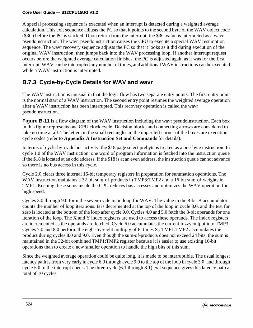
Core User Guide — S12CPU15UG V1.2
get codeavr
ptionof theest firstuted
ointration
oxred tocution
ion. Ineueadvance
. Thention for
atorst for
or oneegisters TMP3.
sum is
ongestough path a
A special processing sequence is executed when an interrupt is detected during a weighted averacalculation. This exit sequence adjusts the PC so that it points to the second byte of the WAV objec($3C) before the PC is stacked. Upon return from the interrupt, the $3C value is interpreted as a wpseudoinstruction. The wavr pseudoinstruction causes the CPU to execute a special WAV resumsequence. The wavr recovery sequence adjusts the PC so that it looks as it did during execution original WAV instruction, then jumps back into the WAV processing loop. If another interrupt requoccurs before the weighted average calculation finishes, the PC is adjusted again as it was for theinterrupt. WAV can be interrupted any number of times, and additional WAV instructions can be execwhile a WAV instruction is interrupted.
B.7.3 Cycle-by-Cycle Details for WAV and wavr
The WAV instruction is unusual in that the logic flow has two separate entry points. The first entry pis the normal start of a WAV instruction. The second entry point resumes the weighted average opeafter a WAV instruction has been interrupted. This recovery operation is called the wavrpseudoinstruction.
Figure B-11 is a flow diagram of the WAV instruction including the wavr pseudoinstruction. Each bin this figure represents one CPU clock cycle. Decision blocks and connecting arrows are considetake no time at all. The letters in the small rectangles in the upper left corner of the boxes are execycle codes (refer toAppendix A Instruction Set and Commands for details).
In terms of cycle-by-cycle bus activity, the $18 page select prebyte is treated as a one-byte instructcycle 1.0 of the WAV instruction, one word of program information is fetched into the instruction quif the $18 is located at an odd address. If the $18 is at an even address, the instruction queue cannotso there is no bus access in this cycle.
Cycle 2.0 clears three internal 16-bit temporary registers in preparation for summation operationsWAV instruction maintains a 32-bit sum-of-products in TMP3:TMP2 and a 16-bit sum-of-weights iTMP1. Keeping these sums inside the CPU reduces bus accesses and optimizes the WAV operahigh speed.
Cycles 3.0 through 9.0 form the seven-cycle main loop for WAV. The value in the 8-bit B accumulcounts the number of loop iterations. B is decremented at the top of the loop in cycle 3.0, and the tezero is located at the bottom of the loop after cycle 9.0. Cycles 4.0 and 5.0 fetch the 8-bit operands fiteration of the loop. The X and Y index registers are used to access these operands. The index rare incremented as the operands are fetched. Cycle 6.0 accumulates the current fuzzy output intoCycles 7.0 and 8.0 perform the eight-by-eight multiply of Fi times Si. TMP1:TMP2 accumulates theproduct during cycles 8.0 and 9.0. Even though the sum-of-products does not exceed 24 bits, themaintained in the 32-bit combined TMP1:TMP2 register because it is easier to use existing 16-bitoperations than to create a new smaller operation to handle the high bits of this sum.
Since the weighted average operation could be quite long, it is made to be interruptible. The usual llatency path is from very early in cycle 6.0 through cycle 9.0 to the top of the loop in cycle 3.0, and thrcycle 5.0 to the interrupt check. The three-cycle (6.1 through 8.1) exit sequence gives this latencytotal of 10 cycles.
524
Core User Guide — S12CPU15UG V1.2
ed to
oesn’tat thefrom
n case
If the WAV instruction is interrupted, the internal temporary registers TMP3, TMP2, and TMP1 nebe stored on the stack so that the operation can be resumed. Since the WAV instruction includesinitialization in cycle 2.0, the recovery path after an interrupt needs to be different. The wavrpseudoinstruction has the same opcode as WAV, but it is on the first page of the opcode map so it dhave the $18 page 2 prebyte that WAV has. When WAV is interrupted, the PC is adjusted to pointsecond byte of the WAV object code, so that it is interpreted as the wavr pseudoinstruction on returnthe interrupt, rather than the WAV instruction. During the recovery sequence, the PC is readjusted ianother interrupt comes before the weighted average operation finishes.
525
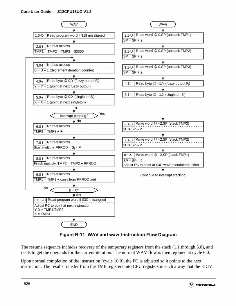
Core User Guide — S12CPU15UG V1.2
0), and6.0.
EDIV
Figure B-11 WAV and wavr Instruction Flow Diagram
The resume sequence includes recovery of the temporary registers from the stack (1.1 through 5.reads to get the operands for the current iteration. The normal WAV flow is then rejoined at cycle
Upon normal completion of the instruction (cycle 10.0), the PC is adjusted so it points to the nextinstruction. The results transfer from the TMP registers into CPU registers in such a way that the
Interrupt pending?
1.0-O Read program word if $18 misaligned
2.0-f No bus access
TMP1 = TMP2 = TMP3 = $0000
WAV
END
No
Yes
Continue to interrupt stacking
6.0-f No bus access
TMP3 = TMP3 + Fi
8.1-S Write word @ –2,SP (stack TMP1)
SP = SP – 2Adjust PC to point at $3C wavr pseudoinstruction
3.0-f No bus access
B = B – 1 (decrement iteration counter)
4.0-r Read byte @ 0,Y (fuzzy output Fi)
Y = Y + 1 (point at next fuzzy output)
5.0-r Read byte @ 0,X (singleton Si)
X = X + 1 (point at next singleton)
1.1-U Read word @ 0,SP (unstack TMP1)
SP = SP + 2
WAVr
2.1-U Read word @ 0,SP (unstack TMP2)
SP = SP + 2
3.1-U Read word @ 0,SP (unstack TMP3)
SP = SP + 2
4.1-r Read byte @ –1,Y (fuzzy output Fi)
5.1-r Read byte @ –1,X (singleton Si)
7.0-f No bus access
Start multiply, PPROD = Si × Fi
8.0-f No bus access
Finish multiply, TMP2 = TMP2 + PPROD
9.0-f No bus access
TMP1 = TMP1 + carry from PPROD add
B = 0?No
10.0 –O Read program word if $3C misaligned
Adjust PC to point at next instructionY:D = TMP1:TMP2X = TMP3
6.1-S Write word @ –2,SP (stack TMP3)
SP = SP – 2
7.1-S Write word @ –2,SP (stack TMP2)
SP = SP – 2
Yes
526

Core User Guide — S12CPU15UG V1.2
and
ations,some
tedctions
tionstions.edssible
r,tical forL and
ctionffectivee lineTBL.
ent
e
at dealidth
is thenent of
instruction can divide the sum-of-products by the sum-of-weights. TMP1:TMP2 transfers into Y:D TMP3 transfers into X.
B.8 Custom Fuzzy Logic Programming
The basic fuzzy logic inference techniques described above are suitable for a broad range of applicbut some systems may require customization. The built-in fuzzy instructions use 8-bit resolution andsystems may require finer resolution. The rule evaluation instructions support only variations ofMIN-MAX rule evaluation. Other methods have been discussed in fuzzy logic literature. The weighaverage of singletons is not the only defuzzification technique. The HCS12 CPU has several instruand addressing modes that can be helpful in developing custom fuzzy logic systems.
B.8.1 Fuzzification Variations
The MEM instruction supports trapezoidal and several other membership functions, including funcwith vertical (infinite slope) sides. Triangular membership functions are a subset of trapezoidal funcSome practitioners refer to s-, z-, andπ-shaped membership functions. These refer to trapezoids buttagainst the right, left, or neither end of the x-axis. Many other membership function shapes are powith sufficient memory space and processing bandwidth.
Tabular membership functions offer total flexibility in shape and very fast evaluation time. Howevetables take as many as 256 bytes of memory space per system input label. This makes them impracmost microcontroller-based fuzzy systems. The HCS12 instruction set includes two instructions, TBETBL, for lookup and interpolation of compressed tables.
The TBL instruction uses 8-bit table entries (y-values) and returns an 8-bit result. The ETBL instruuses 16-bit table entries (y-values) and returns a 16-bit result. Indexed addressing identifies the eaddress of the data point at the beginning of the line segment. The data value for the end point of thsegment is the next consecutive memory location. The data values are bytes for TBL and words for EIn both cases, the B accumulator contains the ratio
The value in B is treated as an 8-bit binary fraction with radix point left of the MSB, so each line segmcan effectively be divided into 256 pieces. During execution of the TBL or ETBL instruction, thedifference between the end point y-value and the beginning point y-value (a signed byte-TBL orword-ETBL) is multiplied by the B accumulator to get an intermediate delta-y term. The result is thy-value of the beginning point, plus this signed intermediate delta-y value.
Because indexed addressing identifies the starting point of the line segment of interest, there is a greof flexibility in constructing tables. A common method is to break the x-axis range into 256 equal wsegments and store the y value for each of the resulting 257 endpoints. The 16-bit D accumulatorthe x input to the table. The upper eight bits in A are used as a coarse lookup to find the line segminterest, and the lower eight bits in B are used to interpolate within this line segment.
In the program sequence:
x-distance from beginning of line segment to lookup pointx-distance from beginning to end of line segment
-------------------------------------------------------------------------------------------------------------------------------------------------------
527
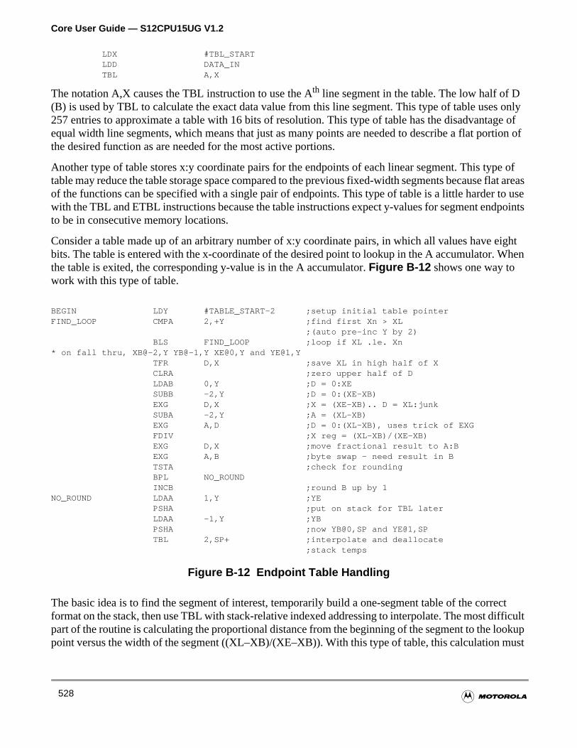
Core User Guide — S12CPU15UG V1.2
s onlyge ofrtion of
pe oflat areasuse
points
eighthen
ectfficultokupust
LDX #TBL_STARTLDD DATA_INTBL A,X
The notation A,X causes the TBL instruction to use the Ath line segment in the table. The low half of D(B) is used by TBL to calculate the exact data value from this line segment. This type of table use257 entries to approximate a table with 16 bits of resolution. This type of table has the disadvantaequal width line segments, which means that just as many points are needed to describe a flat pothe desired function as are needed for the most active portions.
Another type of table stores x:y coordinate pairs for the endpoints of each linear segment. This tytable may reduce the table storage space compared to the previous fixed-width segments because fof the functions can be specified with a single pair of endpoints. This type of table is a little harder towith the TBL and ETBL instructions because the table instructions expect y-values for segment endto be in consecutive memory locations.
Consider a table made up of an arbitrary number of x:y coordinate pairs, in which all values have bits. The table is entered with the x-coordinate of the desired point to lookup in the A accumulator. Wthe table is exited, the corresponding y-value is in the A accumulator.Figure B-12 shows one way towork with this type of table.
BEGIN LDY #TABLE_START-2 ;setup initial table pointerFIND_LOOP CMPA 2,+Y ;find first Xn > XL
;(auto pre-inc Y by 2)BLS FIND_LOOP ;loop if XL .le. Xn
* on fall thru, XB@-2,Y YB@-1,Y XE@0,Y and YE@1,YTFR D,X ;save XL in high half of XCLRA ;zero upper half of DLDAB 0,Y ;D = 0:XESUBB -2,Y ;D = 0:(XE-XB)EXG D,X ;X = (XE-XB).. D = XL:junkSUBA -2,Y ;A = (XL-XB)EXG A,D ;D = 0:(XL-XB), uses trick of EXGFDIV ;X reg = (XL-XB)/(XE-XB)EXG D,X ;move fractional result to A:BEXG A,B ;byte swap - need result in BTSTA ;check for roundingBPL NO_ROUNDINCB ;round B up by 1
NO_ROUND LDAA 1,Y ;YEPSHA ;put on stack for TBL laterLDAA -1,Y ;YBPSHA ;now YB@0,SP and YE@1,SPTBL 2,SP+ ;interpolate and deallocate
;stack temps
Figure B-12 Endpoint Table Handling
The basic idea is to find the segment of interest, temporarily build a one-segment table of the corrformat on the stack, then use TBL with stack-relative indexed addressing to interpolate. The most dipart of the routine is calculating the proportional distance from the beginning of the segment to the lopoint versus the width of the segment ((XL–XB)/(XE–XB)). With this type of table, this calculation m
528
Core User Guide — S12CPU15UG V1.2
order
ibutionlve for. Such
t there thet ananingr asense
dual
aonwithin
ork
lace therencest input
, so thislator,exed
there isd fuzzy
nd.lution
be done at run time. In the previous type of table, this proportional term is an inherent part (the lowestbits) of the data input to the table.
Some fuzzy theorists have suggested that membership functions should be shaped like normal distrcurves or other mathematical functions. This may be correct, but the processing requirements to soan intercept on such a function would be unacceptable for most microcontroller-based fuzzy systemsa function could be encoded into a table of one of the previously described types.
For many common systems, the thing that is most important about membership function shape is thais a gradual transition from nonmembership to membership as the system input value approachescentral range of the membership function. Let us examine the human problem of stopping a car aintersection. We might use rules like “If intersection is close and speed is fast, apply brakes.” The meof the labels “close” and “fast”, reflected in membership function shape and position, is different foteenager than it is for a grandmother, but both can accomplish the goal of stopping. It makes intuitivethat the exact shape of a membership function is much less important than the fact that it has graboundaries.
B.8.2 Rule Evaluation Variations
The REV and REVW instructions expect fuzzy input and fuzzy output values to be 8-bit values. Incustom fuzzy inference program, higher resolution may be desirable, although this is not a commrequirement. The HCS12 CPU includes variations of minimum and maximum operations that workthe fuzzy MIN-MAX inference algorithm. The problem with the fuzzy inference algorithm is that the mand max operations need to store their results differently, so the min and max instructions must wdifferently or more than one variation of these instructions is needed.
The HCS12 CPU has min and max instructions for 8- or 16-bit operands, with one operand in anaccumulator and the other in a referenced memory location. There are separate variations that repaccumulator or the memory location with the result. While processing rule antecedents in a fuzzy infeprogram, a reference value must be compared to each of the referenced fuzzy inputs, and the smallemust end up in an accumulator. The instruction:
EMIND 2,X+ ;process one rule antecedent
automates the central operations needed to process rule antecedents. The E stands for extendedinstruction compares 16-bit operands. The D at the end of the mnemonic stands for the D accumuwhich is both the first operand for the comparison and the destination of the result. The 2,X+ is an indaddressing specification that says X points to the second operand for the comparison.
When processing rule consequents, the operand in the accumulator must remain constant in casemore than one consequent in the rule, and the result of the comparison must replace the referenceoutput in RAM. To do this, use the instruction:
EMAXM 2,X+ ;process one rule consequent
The M at the end of the mnemonic indicates that the result replaces the referenced memory operaAgain, indexed addressing is used. These two instructions can form the working part of a 16-bit resofuzzy inference routine.
529
Core User Guide — S12CPU15UG V1.2
sed.rogram
than
tines. an
r foructionth6-bit
ained,such a
ause it
roachsen maxlogic
rage.
CSly
result
There are many other methods of performing inference, but the min-max method is most widely uSince the HCS12 is a general-purpose microcontroller, the programmer has complete freedom to pany algorithm desired. A custom algorithm would typically take more code space and execution timea routine that used the built-in REV or REVW instructions.
B.8.3 Defuzzification Variations
There are two main areas where other HCS12 instructions can help with custom defuzzification rouThe first case is working with operands with more than eight bits. The second case involves usingentirely different approach than weighted average of singletons.
The primary part of the WAV instruction is a multiply and accumulate operation to get the numeratothe weighted average calculation. When working with operands as large as 16 bits, the EMACS instrcould at least automate the multiply and accumulate function. The HCS12 CPU has extended macapabilities, including 32-bit by 16-bit divide instructions and the EMACS instruction which uses 1input operands and accumulates the sum to a 32-bit memory location.
One benefit of the WAV instruction is that both a sum of products and a sum of weights are maintwhile the fuzzy output operand is only accessed from memory once. Since memory access time issignificant part of execution time, this provides a speed advantage over conventional instructions.
The weighted average of singletons is the most commonly used technique in microcontrollers becis computationally less difficult than most other methods. The simplest method is called maxdefuzzification, which simply uses the largest fuzzy output as the system result. However, this appdoes not take into account any other fuzzy outputs, even when they are almost as true as the chooutput. Max defuzzification is not a good general choice because it only works for a subset of fuzzyapplications.
The HCS12 CPU is well suited for more computationally challenging algorithms than weighted aveA 32-bit by 16-bit divide instruction takes eleven or twelve 8-MHz cycles for unsigned or signedvariations. A 16-bit by 16-bit multiply with a 32-bit result takes only three 8-MHz cycles. The EMAinstruction uses 16-bit operands and accumulates the result in a 32-bit memory location, taking ontwelve 8-MHz cycles per iteration, including accessing all operands from memory and storing the to memory.
530
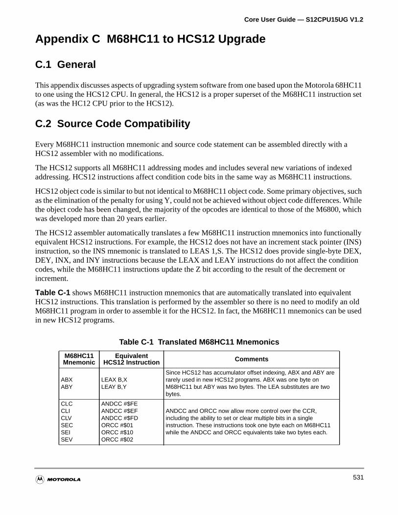
Core User Guide — S12CPU15UG V1.2
8HC11ion set
a
xedns.
suchhile
, which
nallyr (INS) DEX,ionr
ntan oldused
Appendix C M68HC11 to HCS12 Upgrade
C.1 General
This appendix discusses aspects of upgrading system software from one based upon the Motorola 6to one using the HCS12 CPU. In general, the HCS12 is a proper superset of the M68HC11 instruct(as was the HC12 CPU prior to the HCS12).
C.2 Source Code Compatibility
Every M68HC11 instruction mnemonic and source code statement can be assembled directly withHCS12 assembler with no modifications.
The HCS12 supports all M68HC11 addressing modes and includes several new variations of indeaddressing. HCS12 instructions affect condition code bits in the same way as M68HC11 instructio
HCS12 object code is similar to but not identical to M68HC11 object code. Some primary objectives,as the elimination of the penalty for using Y, could not be achieved without object code differences. Wthe object code has been changed, the majority of the opcodes are identical to those of the M6800was developed more than 20 years earlier.
The HCS12 assembler automatically translates a few M68HC11 instruction mnemonics into functioequivalent HCS12 instructions. For example, the HCS12 does not have an increment stack pointeinstruction, so the INS mnemonic is translated to LEAS 1,S. The HCS12 does provide single-byteDEY, INX, and INY instructions because the LEAX and LEAY instructions do not affect the conditcodes, while the M68HC11 instructions update the Z bit according to the result of the decrement oincrement.
Table C-1 shows M68HC11 instruction mnemonics that are automatically translated into equivaleHCS12 instructions. This translation is performed by the assembler so there is no need to modify M68HC11 program in order to assemble it for the HCS12. In fact, the M68HC11 mnemonics can bein new HCS12 programs.
Table C-1 Translated M68HC11 Mnemonics
M68HC11Mnemonic
EquivalentHCS12 Instruction Comments
ABXABY
LEAX B,XLEAY B,Y
Since HCS12 has accumulator offset indexing, ABX and ABY arerarely used in new HCS12 programs. ABX was one byte onM68HC11 but ABY was two bytes. The LEA substitutes are twobytes.
CLCCLICLVSECSEISEV
ANDCC #$FEANDCC #$EFANDCC #$FDORCC #$01ORCC #$10ORCC #$02
ANDCC and ORCC now allow more control over the CCR,including the ability to set or clear multiple bits in a singleinstruction. These instructions took one byte each on M68HC11while the ANDCC and ORCC equivalents take two bytes each.
531
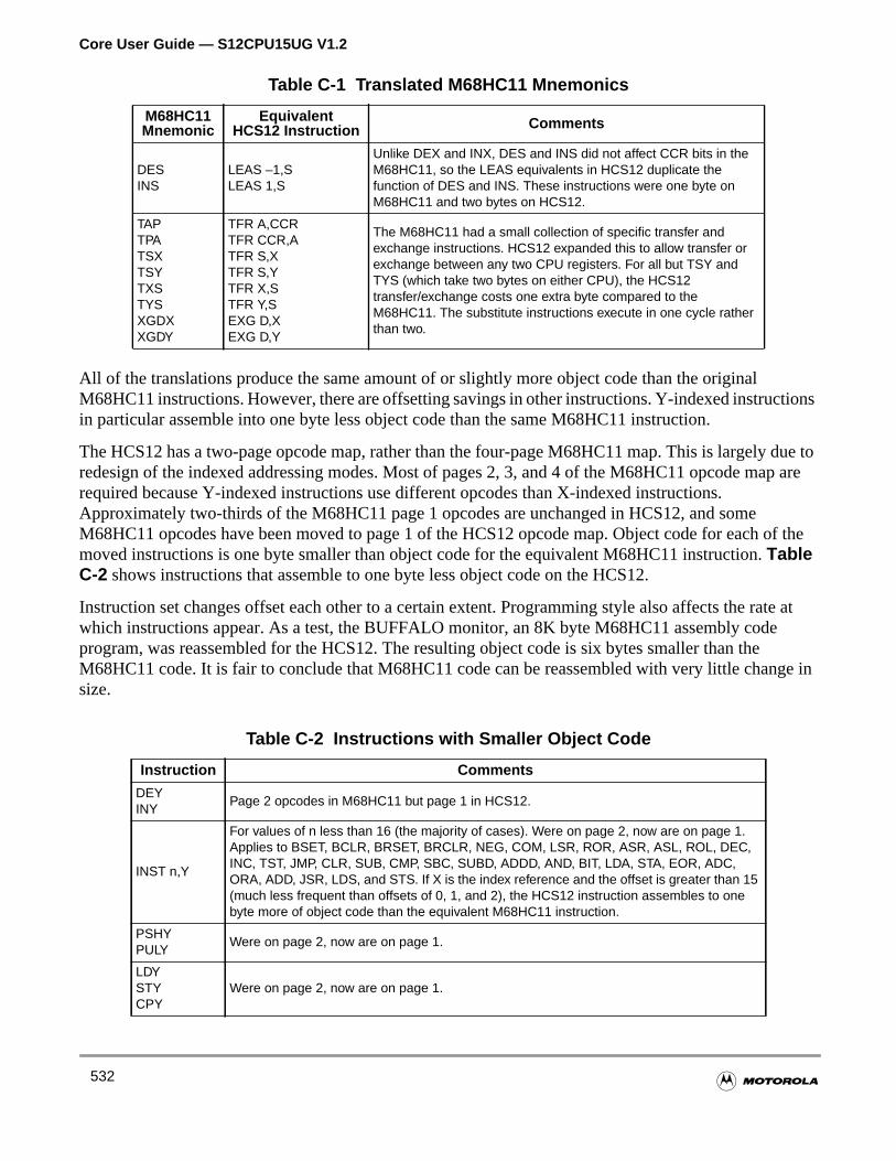
Core User Guide — S12CPU15UG V1.2
tions
due toap are
of the
te at
ge in
All of the translations produce the same amount of or slightly more object code than the originalM68HC11 instructions. However, there are offsetting savings in other instructions. Y-indexed instrucin particular assemble into one byte less object code than the same M68HC11 instruction.
The HCS12 has a two-page opcode map, rather than the four-page M68HC11 map. This is largelyredesign of the indexed addressing modes. Most of pages 2, 3, and 4 of the M68HC11 opcode mrequired because Y-indexed instructions use different opcodes than X-indexed instructions.Approximately two-thirds of the M68HC11 page 1 opcodes are unchanged in HCS12, and someM68HC11 opcodes have been moved to page 1 of the HCS12 opcode map. Object code for eachmoved instructions is one byte smaller than object code for the equivalent M68HC11 instruction.TableC-2 shows instructions that assemble to one byte less object code on the HCS12.
Instruction set changes offset each other to a certain extent. Programming style also affects the rawhich instructions appear. As a test, the BUFFALO monitor, an 8K byte M68HC11 assembly codeprogram, was reassembled for the HCS12. The resulting object code is six bytes smaller than theM68HC11 code. It is fair to conclude that M68HC11 code can be reassembled with very little chansize.
DESINS
LEAS –1,SLEAS 1,S
Unlike DEX and INX, DES and INS did not affect CCR bits in theM68HC11, so the LEAS equivalents in HCS12 duplicate thefunction of DES and INS. These instructions were one byte onM68HC11 and two bytes on HCS12.
TAPTPATSXTSYTXSTYSXGDXXGDY
TFR A,CCRTFR CCR,ATFR S,XTFR S,YTFR X,STFR Y,SEXG D,XEXG D,Y
The M68HC11 had a small collection of specific transfer andexchange instructions. HCS12 expanded this to allow transfer orexchange between any two CPU registers. For all but TSY andTYS (which take two bytes on either CPU), the HCS12transfer/exchange costs one extra byte compared to theM68HC11. The substitute instructions execute in one cycle ratherthan two.
Table C-2 Instructions with Smaller Object Code
Instruction Comments
DEYINY
Page 2 opcodes in M68HC11 but page 1 in HCS12.
INST n,Y
For values of n less than 16 (the majority of cases). Were on page 2, now are on page 1.Applies to BSET, BCLR, BRSET, BRCLR, NEG, COM, LSR, ROR, ASR, ASL, ROL, DEC,INC, TST, JMP, CLR, SUB, CMP, SBC, SUBD, ADDD, AND, BIT, LDA, STA, EOR, ADC,ORA, ADD, JSR, LDS, and STS. If X is the index reference and the offset is greater than 15(much less frequent than offsets of 0, 1, and 2), the HCS12 instruction assembles to onebyte more of object code than the equivalent M68HC11 instruction.
PSHYPULY
Were on page 2, now are on page 1.
LDYSTYCPY
Were on page 2, now are on page 1.
Table C-1 Translated M68HC11 Mnemonics
M68HC11Mnemonic
EquivalentHCS12 Instruction Comments
532
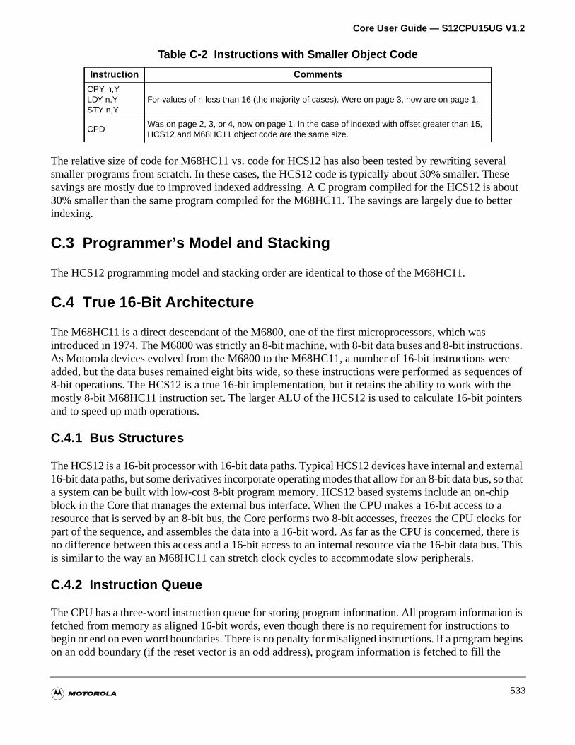
Core User Guide — S12CPU15UG V1.2
ralhese aboutetter
tions.reences ofheters
ternalso thatchip to aocks for there isus. This
on iss toeginse
The relative size of code for M68HC11 vs. code for HCS12 has also been tested by rewriting sevesmaller programs from scratch. In these cases, the HCS12 code is typically about 30% smaller. Tsavings are mostly due to improved indexed addressing. A C program compiled for the HCS12 is30% smaller than the same program compiled for the M68HC11. The savings are largely due to bindexing.
C.3 Programmer’s Model and Stacking
The HCS12 programming model and stacking order are identical to those of the M68HC11.
C.4 True 16-Bit Architecture
The M68HC11 is a direct descendant of the M6800, one of the first microprocessors, which wasintroduced in 1974. The M6800 was strictly an 8-bit machine, with 8-bit data buses and 8-bit instrucAs Motorola devices evolved from the M6800 to the M68HC11, a number of 16-bit instructions weadded, but the data buses remained eight bits wide, so these instructions were performed as sequ8-bit operations. The HCS12 is a true 16-bit implementation, but it retains the ability to work with tmostly 8-bit M68HC11 instruction set. The larger ALU of the HCS12 is used to calculate 16-bit poinand to speed up math operations.
C.4.1 Bus Structures
The HCS12 is a 16-bit processor with 16-bit data paths. Typical HCS12 devices have internal and ex16-bit data paths, but some derivatives incorporate operating modes that allow for an 8-bit data bus,a system can be built with low-cost 8-bit program memory. HCS12 based systems include an on-block in the Core that manages the external bus interface. When the CPU makes a 16-bit accessresource that is served by an 8-bit bus, the Core performs two 8-bit accesses, freezes the CPU clpart of the sequence, and assembles the data into a 16-bit word. As far as the CPU is concerned,no difference between this access and a 16-bit access to an internal resource via the 16-bit data bis similar to the way an M68HC11 can stretch clock cycles to accommodate slow peripherals.
C.4.2 Instruction Queue
The CPU has a three-word instruction queue for storing program information. All program informatifetched from memory as aligned 16-bit words, even though there is no requirement for instructionbegin or end on even word boundaries. There is no penalty for misaligned instructions. If a program bon an odd boundary (if the reset vector is an odd address), program information is fetched to fill th
CPY n,YLDY n,YSTY n,Y
For values of n less than 16 (the majority of cases). Were on page 3, now are on page 1.
CPDWas on page 2, 3, or 4, now on page 1. In the case of indexed with offset greater than 15,HCS12 and M68HC11 object code are the same size.
Table C-2 Instructions with Smaller Object Code
Instruction Comments
533
Core User Guide — S12CPU15UG V1.2
reset
de)
ueue
ue toinesquence
ins. and
ith anlignedd withnnote, the
gramnd the
the, theen usedng
t aware
ignalsionn toaddress
bytes,fixed
allowl RAM,nment.
instruction queue, beginning with an aligned word read at the natural boundary of the misaligned vector. The instruction queue logic starts execution with the opcode in the low half of this word.
The instruction queue makes three bytes of program information (starting with the instruction opcodirectly available to the CPU at the beginning of every instruction. As each instruction executes, itperforms enough additional program fetches to refill the space it took up in the queue. Alignmentinformation is maintained by logic in the instruction queue. The CPU provides signals that tell the qlogic when to advance a word of program information, and when to toggle the alignment status.
The CPU is not aware of instruction alignment. The queue logic sorts out the information in the quepresent the opcode and additional bytes of information as CPU inputs. A control algorithm determwhether the opcode is in the even or odd half of the word at the head of the queue. The execution sefor all instructions is independent of the alignment of the instruction.
The only situation in which alignment can affect the number of cycles an instruction takes occurs devices that have a narrow (8-bit) external data bus, and is related to optional program fetch cycleOptional cycles are always performed, but serve different purposes determined by instruction sizealignment.
Each instruction includes one program fetch cycle for every two bytes of object code. Instructions wodd number of bytes can use an optional cycle to fetch an extra word of object code. If the queue is aat the start of an instruction with an odd byte count, the last byte of object code shares a queue worthe opcode of the next instruction. Since this word holds part of the next instruction, the queue caadvance after the odd byte executes, or the first byte of the next instruction would be lost. In this casoptional cycle appears as a free cycle since the queue is not ready to accept the next word of proinformation. If this same instruction had been misaligned, the queue would be ready to advance aoptional cycle would be used to perform a program word fetch.
In a single-chip system or in a system with the program in 16-bit memory, both the free cycle andprogram fetch cycle take one bus cycle. In a system with the program in an external 8-bit memoryoptional cycle takes one bus cycle when it appears as a free cycle, but it takes two bus cycles whto perform a program fetch. In this case, the on-chip integration module freezes the CPU clocks loenough to perform the cycle as two smaller accesses. The CPU handles only 16-bit data, and is nothat the 16-bit program access is split into two 8-bit accesses.
In order to allow development systems to track events in the HCS12 instruction queue, two status s(IPIPE[1:0]) provide information about data movement in the queue and about the start of instructexecution. A development system can use this information along with address and data informatioexternally reconstruct the queue. This representation of the queue can also track both the data andbuses.
C.4.3 Stack Function
Both the M68HC11 and the HCS12 stack nine bytes for interrupts. Since this is an odd number ofthere is no practical way to assure that the stack will stay aligned. To assure that instructions take anumber of cycles regardless of stack alignment, the internal RAM in HCS12 systems is designed tosingle-cycle 16-bit accesses to misaligned addresses. As long as the stack is located in this speciastacking and unstacking operations take the same amount of execution time, regardless of stack alig
534
Core User Guide — S12CPU15UG V1.2
e thea
t is, theailableation
ithout
f the:01F2;hen up at
TSXt stackng the
, thereer, the
the12,
erate
ldper toontains
ded
h thenbility
ointer.arrive
If the stack is located in an external 16-bit RAM, a PSHX instruction can take two or three cyclesdepending on the alignment of the stack. This extra access time is transparent to the CPU becausintegration module freezes the CPU clocks while it performs the extra 8-bit bus cycle required for misaligned stack operation.
The HCS12 has a last-used stack rather than a next-available stack like the M68HC11 CPU. Thastack pointer points to the last 16-bit stack address used, rather than to the address of the next avstack location. This generally has very little effect, because it is very unusual to access stacked informusing absolute addressing. The change allows a 16-bit word of data to be removed from the stack wchanging the value of the SP twice.
To illustrate, consider the operation of a PULX instruction. With the next-available M68HC11 stack, iSP = $01F0 when execution begins, the sequence of operations is: SP = SP + 1; load X from $01F1SP = SP + 1; and the SP ends up at $01F2. With the last-used HCS12 stack, if the SP = $01F0 wexecution begins, the sequence is: load X from $01F0:01F1; SP = SP + 2; and the SP again ends$01F2. The second sequence requires one less stack pointer adjustment.
The stack pointer change also affects operation of the TSX and TXS instructions. In the M68HC11,increments the SP by one during the transfer. This adjustment causes the X index to point to the laslocation used. The TXS instruction operates similarly, except that it decrements the SP by one duritransfer. HCS12 TSX and TXS instructions are ordinary transfers — the HCS12 stack requires noadjustment.
For ordinary use of the stack, such as pushes, pulls, and even manipulations involving TSX and TXSare no differences in the way the M68HC11 and the HCS12 stacks look to a programmer. Howevstack change can affect a program algorithm in two subtle ways.
The LDS #$xxxx instruction is normally used to initialize the stack pointer at the start of a program. InM68HC11, the address specified in the LDS instruction is the first stack location used. In the HCShowever, the first stack location used is one address lower than the address specified in the LDSinstruction. Since the stack builds downward, M68HC11 programs reassembled for the HCS12 opnormally, but the program stack is one physical address lower in memory.
In very uncommon situations, such as test programs used to verify CPU operation, a program couinitialize the SP, stack data, and then read the stack via an extended mode read (it is normally improread stack data from an absolute extended address). To make an M68HC11 source program that csuch a sequence work on the HCS12, change either the initial LDS #$xxxx, or the absolute extenaddress used to read the stack.
C.5 Improved Indexing
The HCS12 has significantly improved indexed addressing capability, yet retains compatibility witM68HC11. The one-cycle and one-byte cost of doing Y-related indexing in the M68HC11 has beeeliminated. In addition, high level language requirements, including stack-relative indexing and the ato perform pointer arithmetic directly in the index registers, have been accommodated.
The M68HC11 has one variation of indexed addressing that works from X or Y as the reference pFor X indexed addressing, an 8-bit unsigned offset in the instruction is added to the index pointer to
535
Core User Guide — S12CPU15UG V1.2
bytesembles
e code
tructiond as the, or
atesister,dex
bject
uency
offsetandas thet code
8-bittbyte,
dress68 towo
at the address of the operand for the instruction. A load accumulator instruction assembles into twoof object code, the opcode and a one-byte offset. Using Y as the reference, the same instruction assinto three bytes (a page prebyte, the opcode, and a one-byte offset.) Analysis of M68HC11 sourcindicates that the offset is most frequently zero and very seldom greater than four.
The HCS12 indexed addressing scheme uses a postbyte plus 0, 1, or 2 extension bytes after the insopcode. These bytes specify which index register is used, determine whether an accumulator is useoffset, implement automatic pre/post increment/decrement of indices, and allow a choice of 5-, 9-16-bit signed offsets. This approach eliminates the differences between X and Y register use anddramatically enhances indexed addressing capabilities.
Major improvements that result from this new approach are:
• Stack pointer can be used as an index register in all indexed operations
• Program counter can be used as index register in all but autoinc/dec modes
• Accumulator offsets allowed using A, B, or D accumulators
• Automatic pre- or post-, increment or decrement (by –8 to +8)
• 5-bit, 9-bit, or 16-bit signed constant offsets
• 16-bit offset indexed-indirect and accumulator D offset indexed-indirect
The change completely eliminates pages three and four of the M68HC11 opcode map and eliminalmost all instructions from page two of the opcode map. For offsets of +0 to +15 from the X index regthe object code is the same size as it was for the M68HC11. For offsets of +0 to +15 from the Y inregister, the object code is one byte smaller than it was for the M68HC11.
C.5.1 Constant Offset Indexing
The HCS12 offers three variations of constant offset indexing in order to optimize the efficiency of ocode generation.
The most common constant offset is zero. Offsets of 1, 2,…4 are used fairly often, but with less freqthan zero.
The 5-bit constant offset variation covers the most frequent indexing requirements by including thein the postbyte. This reduces a load accumulator indexed instruction to two bytes of object code, matches the object code size of the smallest M68HC11 indexed instructions, which can only use Xindex register. The HCS12 can use X, Y, SP, or PC as the index reference with no additional objecsize cost.
The signed 9-bit constant offset indexing mode covers the same positive range as the M68HC11 unsigned offset. The size was increased to nine bits with the sign bit (ninth bit) included in the posand the remaining 8-bits of the offset in a single extension byte.
The 16-bit constant offset indexing mode allows indexed access to the entire normal 64K byte adspace. Since the address consists of 16 bits, the 16-bit offset can be regarded as a signed (–32,7+32767) or unsigned (0 to 65,535) value. In 16-bit constant offset mode, the offset is supplied in textension bytes after the opcode and postbyte.
536
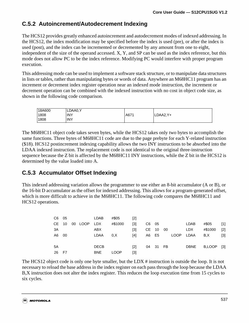
Core User Guide — S12CPU15UG V1.2
ssing. Inex is
, but thisram
ructuresas an ore, as
sh theructiono the
12 is
B), oroffset,d
s note LDAAles to
C.5.2 Autoincrement/Autodecrement Indexing
The HCS12 provides greatly enhanced autoincrement and autodecrement modes of indexed addrethe HCS12, the index modification may be specified before the index is used (pre), or after the indused (post), and the index can be incremented or decremented by any amount from one to eight,independent of the size of the operand accessed. X, Y, and SP can be used as the index referencemode does not allow PC to be the index reference. Modifying PC would interfere with proper progexecution.
This addressing mode can be used to implement a software stack structure, or to manipulate data stin lists or tables, rather than manipulating bytes or words of data. Anywhere an M68HC11 program hincrement or decrement index register operation near an indexed mode instruction, the incrementdecrement operation can be combined with the indexed instruction with no cost in object code sizshown in the following code comparison.
The M68HC11 object code takes seven bytes, while the HCS12 takes only two bytes to accomplisame functions. Three bytes of M68HC11 code are due to the page prebyte for each Y-related inst($18). HCS12 postincrement indexing capability allows the two INY instructions to be absorbed intLDAA indexed instruction. The replacement code is not identical to the original three-instructionsequence because the Z bit is affected by the M68HC11 INY instructions, while the Z bit in the HCSdetermined by the value loaded into A.
C.5.3 Accumulator Offset Indexing
This indexed addressing variation allows the programmer to use either an 8-bit accumulator (A orthe 16-bit D accumulator as the offset for indexed addressing. This allows for a program-generatedwhich is more difficult to achieve in the M68HC11. The following code compares the M68HC11 anHCS12 operations.
The HCS12 object code is only one byte smaller, but the LDX # instruction is outside the loop. It inecessary to reload the base address in the index register on each pass through the loop because thB,X instruction does not alter the index register. This reduces the loop execution time from 15 cycsix cycles.
18A60018081808
LDAA0,YINYINY
A671 LDAA2,Y+
C6 05 LDAB #$05 [2]
CE 10 00 LOOP LDX #$1000 [3] C6 05 LDAB #$05 [1]
3A ABX [3] CE 10 00 LDX #$1000 [2]
A6 00 LDAA 0,X [4] A6 E5 LOOP LDAA B,X [3]
5A DECB [2] 04 31 FB DBNE B,LOOP [3]
26 F7 BNE LOOP [3]
537
Core User Guide — S12CPU15UG V1.2
ationred tosetas in
on usesnters.irectg can
ee size.
at takeral the
uch of
s to
C.5.4 Indirect Indexing
The HCS12 allows some forms of indexed indirect addressing in which the instruction points to a locin memory where the address of the operand is stored. This is an extra level of indirection compaordinary indexed addressing. The two forms of indexed-indirect addressing are 16-bit constant offindexed-indirect and accumulator D indexed-indirect. The indexing register can be X, Y, SP, or PCother HCS12 indexed addressing modes. PC-relative indirect addressing is one of the more commof indexed indirect addressing. The indirect variations of indexed addressing help to implement poiAccumulator D indexed-indirect addressing can implement a runtime-computed GOTO function. Indaddressing is also useful in high level language compilers. For instance, PC-relative indirect indexinefficiently implement some C case statements.
C.6 Improved Performance
HCS12 based systems provide a number of performance improvements over the M68HC11. Thesimprovements include cycle count reduction, faster math instruction execution and reduction of codEach of these aspects is discussed in the subsections below.
C.6.1 Reduced Cycle Counts
No M68HC11 instruction takes less than two cycles, but the HCS12 has more than 50 opcodes thonly one cycle. Some of the reduction comes from the instruction queue, which assures that seveprogram bytes are available at the start of each instruction. Other cycle reductions occur becauseHCS12 can fetch 16 bits of information at a time, rather than eight bits at a time.
C.6.2 Fast Math
The HCS12 has some of the fastest math ever designed into a Motorola general-purpose Core. Mthe speed is due to an execution unit that can perform several operations simultaneously.Table C-3compares the speed of HCS12 and M68HC11 math instructions. The HCS12 requires fewer cycleperform an operation, and the cycle time is half that of the M68HC11.
538
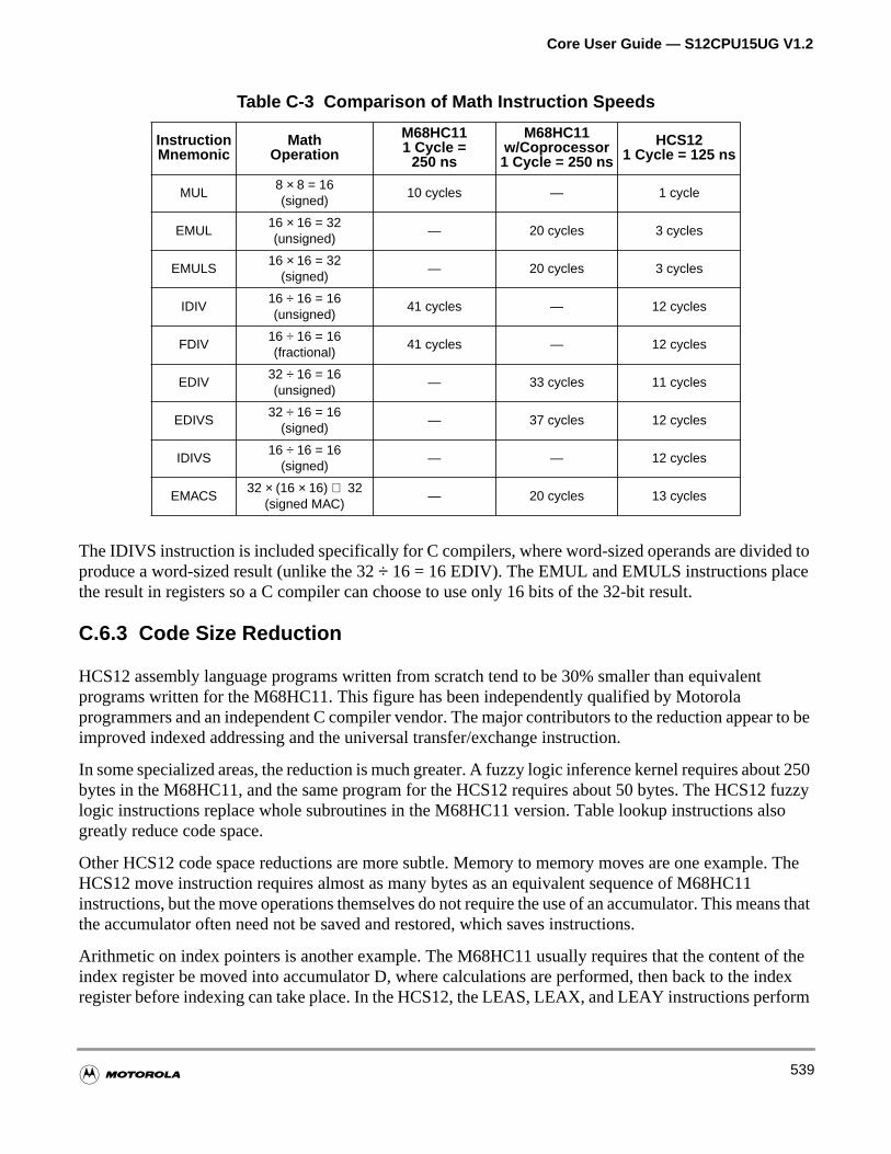
Core User Guide — S12CPU15UG V1.2
d to
t
r to be
ut 250fuzzy
so
le. The
ans that
of thendexform
The IDIVS instruction is included specifically for C compilers, where word-sized operands are divideproduce a word-sized result (unlike the 32÷ 16 = 16 EDIV). The EMUL and EMULS instructions placethe result in registers so a C compiler can choose to use only 16 bits of the 32-bit result.
C.6.3 Code Size Reduction
HCS12 assembly language programs written from scratch tend to be 30% smaller than equivalenprograms written for the M68HC11. This figure has been independently qualified by Motorolaprogrammers and an independent C compiler vendor. The major contributors to the reduction appeaimproved indexed addressing and the universal transfer/exchange instruction.
In some specialized areas, the reduction is much greater. A fuzzy logic inference kernel requires abobytes in the M68HC11, and the same program for the HCS12 requires about 50 bytes. The HCS12logic instructions replace whole subroutines in the M68HC11 version. Table lookup instructions algreatly reduce code space.
Other HCS12 code space reductions are more subtle. Memory to memory moves are one exampHCS12 move instruction requires almost as many bytes as an equivalent sequence of M68HC11instructions, but the move operations themselves do not require the use of an accumulator. This methe accumulator often need not be saved and restored, which saves instructions.
Arithmetic on index pointers is another example. The M68HC11 usually requires that the content index register be moved into accumulator D, where calculations are performed, then back to the iregister before indexing can take place. In the HCS12, the LEAS, LEAX, and LEAY instructions per
Table C-3 Comparison of Math Instruction Speeds
InstructionMnemonic
MathOperation
M68HC111 Cycle =
250 ns
M68HC11w/Coprocessor1 Cycle = 250 ns
HCS121 Cycle = 125 ns
MUL8 × 8 = 16(signed)
10 cycles — 1 cycle
EMUL16 × 16 = 32(unsigned)
— 20 cycles 3 cycles
EMULS16 × 16 = 32
(signed)— 20 cycles 3 cycles
IDIV16 ÷ 16 = 16(unsigned)
41 cycles — 12 cycles
FDIV16 ÷ 16 = 16(fractional)
41 cycles — 12 cycles
EDIV32 ÷ 16 = 16(unsigned)
— 33 cycles 11 cycles
EDIVS32 ÷ 16 = 16
(signed)— 37 cycles 12 cycles
IDIVS16 ÷ 16 = 16
(signed)— — 12 cycles
EMACS32 × (16 × 16) ⇒ 32
(signed MAC)— 20 cycles 13 cycles
539
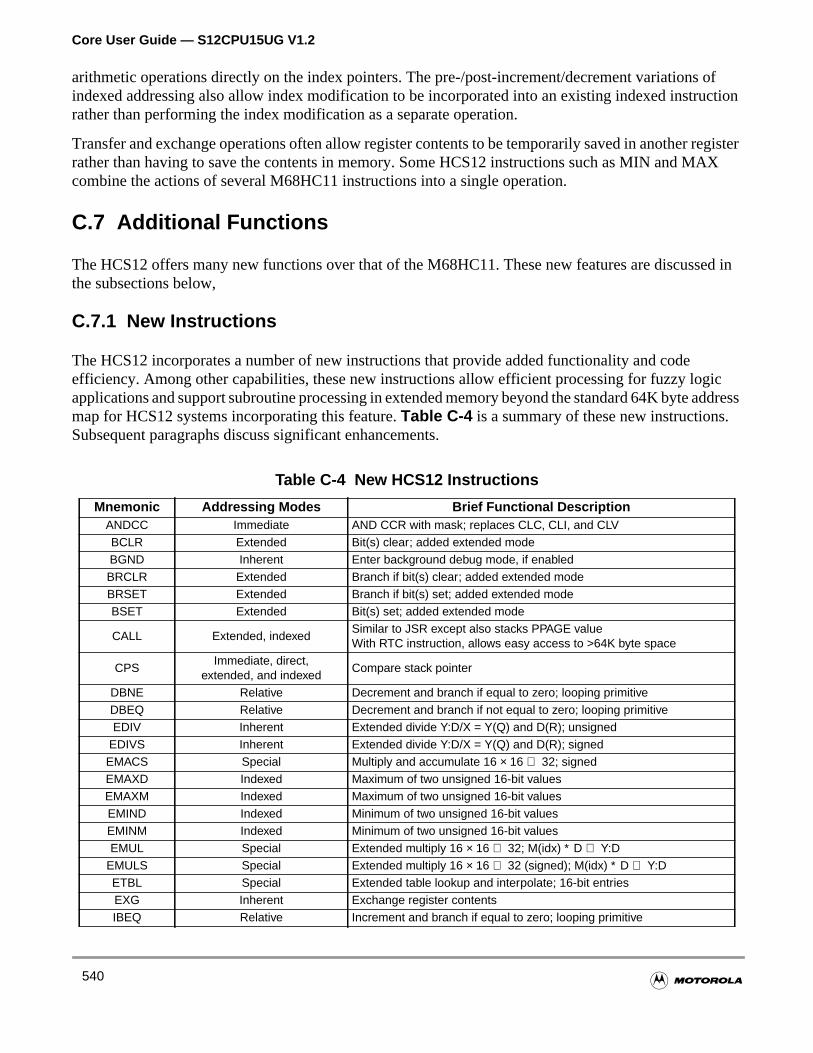
Core User Guide — S12CPU15UG V1.2
ofuction
egisterAX
sed in
icaddress
arithmetic operations directly on the index pointers. The pre-/post-increment/decrement variationsindexed addressing also allow index modification to be incorporated into an existing indexed instrrather than performing the index modification as a separate operation.
Transfer and exchange operations often allow register contents to be temporarily saved in another rrather than having to save the contents in memory. Some HCS12 instructions such as MIN and Mcombine the actions of several M68HC11 instructions into a single operation.
C.7 Additional Functions
The HCS12 offers many new functions over that of the M68HC11. These new features are discusthe subsections below,
C.7.1 New Instructions
The HCS12 incorporates a number of new instructions that provide added functionality and codeefficiency. Among other capabilities, these new instructions allow efficient processing for fuzzy logapplications and support subroutine processing in extended memory beyond the standard 64K bytemap for HCS12 systems incorporating this feature.Table C-4 is a summary of these new instructions.Subsequent paragraphs discuss significant enhancements.
Table C-4 New HCS12 Instructions
Mnemonic Addressing Modes Brief Functional DescriptionANDCC Immediate AND CCR with mask; replaces CLC, CLI, and CLVBCLR Extended Bit(s) clear; added extended modeBGND Inherent Enter background debug mode, if enabledBRCLR Extended Branch if bit(s) clear; added extended modeBRSET Extended Branch if bit(s) set; added extended modeBSET Extended Bit(s) set; added extended mode
CALL Extended, indexedSimilar to JSR except also stacks PPAGE valueWith RTC instruction, allows easy access to >64K byte space
CPSImmediate, direct,
extended, and indexedCompare stack pointer
DBNE Relative Decrement and branch if equal to zero; looping primitiveDBEQ Relative Decrement and branch if not equal to zero; looping primitiveEDIV Inherent Extended divide Y:D/X = Y(Q) and D(R); unsigned
EDIVS Inherent Extended divide Y:D/X = Y(Q) and D(R); signedEMACS Special Multiply and accumulate 16 × 16 ⇒ 32; signedEMAXD Indexed Maximum of two unsigned 16-bit valuesEMAXM Indexed Maximum of two unsigned 16-bit valuesEMIND Indexed Minimum of two unsigned 16-bit valuesEMINM Indexed Minimum of two unsigned 16-bit valuesEMUL Special Extended multiply 16 × 16 ⇒ 32; M(idx) ∗ D ⇒ Y:D
EMULS Special Extended multiply 16 × 16 ⇒ 32 (signed); M(idx) ∗ D ⇒ Y:DETBL Special Extended table lookup and interpolate; 16-bit entriesEXG Inherent Exchange register contentsIBEQ Relative Increment and branch if equal to zero; looping primitive
540
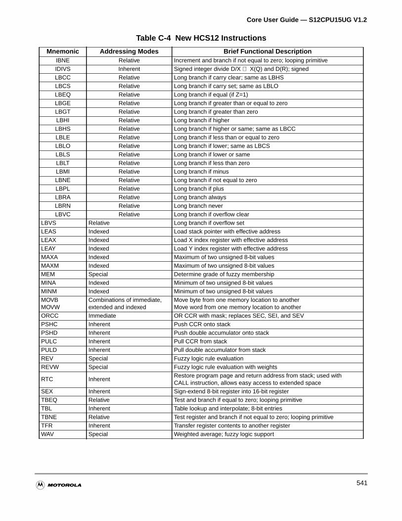
Core User Guide — S12CPU15UG V1.2
IBNE Relative Increment and branch if not equal to zero; looping primitiveIDIVS Inherent Signed integer divide D/X ⇒ X(Q) and D(R); signedLBCC Relative Long branch if carry clear; same as LBHSLBCS Relative Long branch if carry set; same as LBLOLBEQ Relative Long branch if equal (if Z=1)LBGE Relative Long branch if greater than or equal to zeroLBGT Relative Long branch if greater than zeroLBHI Relative Long branch if higherLBHS Relative Long branch if higher or same; same as LBCCLBLE Relative Long branch if less than or equal to zeroLBLO Relative Long branch if lower; same as LBCSLBLS Relative Long branch if lower or sameLBLT Relative Long branch if less than zeroLBMI Relative Long branch if minusLBNE Relative Long branch if not equal to zeroLBPL Relative Long branch if plusLBRA Relative Long branch alwaysLBRN Relative Long branch neverLBVC Relative Long branch if overflow clear
LBVS Relative Long branch if overflow setLEAS Indexed Load stack pointer with effective addressLEAX Indexed Load X index register with effective addressLEAY Indexed Load Y index register with effective addressMAXA Indexed Maximum of two unsigned 8-bit valuesMAXM Indexed Maximum of two unsigned 8-bit valuesMEM Special Determine grade of fuzzy membershipMINA Indexed Minimum of two unsigned 8-bit valuesMINM Indexed Minimum of two unsigned 8-bit valuesMOVBMOVW
Combinations of immediate,extended and indexed
Move byte from one memory location to anotherMove word from one memory location to another
ORCC Immediate OR CCR with mask; replaces SEC, SEI, and SEVPSHC Inherent Push CCR onto stackPSHD Inherent Push double accumulator onto stackPULC Inherent Pull CCR from stackPULD Inherent Pull double accumulator from stackREV Special Fuzzy logic rule evaluationREVW Special Fuzzy logic rule evaluation with weights
RTC InherentRestore program page and return address from stack; used withCALL instruction, allows easy access to extended space
SEX Inherent Sign-extend 8-bit register into 16-bit registerTBEQ Relative Test and branch if equal to zero; looping primitiveTBL Inherent Table lookup and interpolate; 8-bit entriesTBNE Relative Test register and branch if not equal to zero; looping primitiveTFR Inherent Transfer register contents to another registerWAV Special Weighted average; fuzzy logic support
Table C-4 New HCS12 Instructions
Mnemonic Addressing Modes Brief Functional Description
541
Core User Guide — S12CPU15UG V1.2
eaddressions is not
oving
ulator
s awo CPUer-bit-extend
to makeing a callompact
nsnonzeroanchbranch
em
C.7.2 Memory-to-Memory Moves
The HCS12 has both 8- and 16-bit variations of memory-to-memory move instructions. The sourcaddress can be specified with immediate, extended, or indexed addressing modes. The destinationcan be specified by extended or indexed addressing mode. Indexed addressing for move instructlimited to direct indexing modes that require no extension bytes (9- and 16-bit constant offsets areallowed). This leaves the 5-bit signed constant offset, accumulator offset, and theautoincrement/decrement modes. The following simple loop is a block move routine capable of mup to 256 words of information from one memory area to another:
LOOP MOVW 2,X+ , 2,Y+ ;move a word and update pointersDBNE B,LOOP ;repeat B times
The move immediate to extended is a convenient way to initialize a register without using an accumor affecting condition codes.
C.7.3 Universal Transfer and Exchange
The M68HC11 has only eight transfer instructions and two exchange instructions. The HCS12 hauniversal transfer/exchange instruction that can be used to transfer or exchange data between any tregisters. The operation is obvious when the two registers are the same size, and some of the othcombinations provide very useful results. For example when an 8-bit register is transferred to a 16register, a sign-extend operation is performed. Other combinations can be used to perform a zerooperation.
These instructions are used often in HCS12 assembly language programs. Transfers can be usedextra copies of data in another register, and exchanges can be used to temporarily save data durto a routine that expects data in a specific register. This is sometimes faster and produces more cobject code than saving data to memory with pushes or stores.
C.7.4 Loop Construct
The HCS12 instruction set includes a new family of six loop primitive instructions. These instructiodecrement, increment, or test a loop count in a CPU register and then branch based on a zero or test result. The CPU registers that can be used for the loop count are A, B, D, X, Y, or SP. The brrange is a 9-bit signed value (–512 to +511) which gives these instructions twice the range of a shortinstruction.
C.7.5 Long Branches
All of the branch instructions from the M68HC11 are also available with 16-bit offsets which allows thto reach any location in the 64K byte address space.
542
Core User Guide — S12CPU15UG V1.2
tatesas a
AXane
two
1 MINload
kup ore cant legal
.
orten lessobject1
C.7.6 Minimum and Maximum Instructions
Control programs often need to restrict data values within upper and lower limits. The HCS12 facilithis function with 8- and 16-bit versions of MIN and MAX instructions. Each of these instructions hversion that stores the result in either the accumulator or in memory.
For example, in a fuzzy logic inference program, rule evaluation consists of a series of MIN and Moperations. The MIN operation determines the smallest rule input and stores the running result in accumulator. The MAX operation stores the largest rule truth value in an accumulator or stores thprevious fuzzy output value from a RAM location in the fuzzy output in RAM. The following codedemonstrates how MIN and MAX instructions can be used to evaluate a rule with four inputs and outputs.
LDY #OUT1 ;Point at first outputLDX #IN1 ;Point at first input valueLDAA #$FF ;start with largest 8-bit number in AMINA 1,X+ ;A=MIN(A,IN1)MINA 1,X+ ;A=MIN(A,IN2)MINA 1,X+ ;A=MIN(A,IN3)MINA 1,X+ ;A=MIN(A,IN4) so A holds smallest inputMAXM 1,Y+ ;OUT1=MAX(A,OUT1) and A is unchangedMAXM 1,Y+ ;OUT1=MAX(A,OUT2) A still has min input
Before this sequence is executed, the fuzzy outputs must be cleared to zeros (not shown). M68HC1or MAX operations are performed by executing a compare followed by a conditional branch around aor store operation.
These instructions can also be used to limit a data value prior to using it as an input to a table looother routine. Suppose a table is valid for input values between $20 and $7F. An arbitrary input valube tested against these limits and be replaced by the largest legal value if it is too big, or the smallesvalue if too small using the following two HCS12 instructions.
HILIMIT FCB $7F ;comparison value needs to be in memLOWLIMIT FCB $20 ;so it can be referenced via indexedMINA HILIMIT,PCR ;A=MIN(A,$7F)MAXA LOWLIMIT,PCR ;A=MAX(A,$20)
;A now within the legal range $20 to $7F
The “,PCR” notation is also new for the HCS12. This notation indicates the programmer wants anappropriate offset from the PC reference to the memory location (HILIMIT or LOWLIMIT in thisexample), and then to assemble this instruction into a PC-relative indexed MIN or MAX instruction
C.7.7 Fuzzy Logic Support
The HCS12 includes four instructions (MEM, REV, REVW, and WAV) specifically designed to suppfuzzy logic programs. These instructions have a very small impact on the size of the CPU, and evimpact on the cost of a complete MCU. At the same time these instructions dramatically reduce thecode size and execution time for a fuzzy logic inference program. A kernel written for the M68HC1required about 250 bytes. The HCS12 kernel uses about 50 bytes.
543
Core User Guide — S12CPU15UG V1.2
ofof a lineTBL
ing ofemory(the
withtionintt andiate
er toallows
noteould
in thewould
uage do LEASlocal from
ith aching.
C.7.8 Table Lookup and Interpolation
The HCS12 instruction set includes two instructions (TBL and ETBL) for lookup and interpolation compressed tables. Consecutive table values are assumed to be the x coordinates of the endpointssegment. The TBL instruction uses 8-bit table entries (y-values) and returns an 8-bit result. The Einstruction uses 16-bit table entries (y-values) and returns a 16-bit result.
An indexed addressing mode is used to identify the effective address of the data point at the beginnthe line segment, and the data value for the end point of the line segment is the next consecutive mlocation (byte for TBL and word for ETBL). In both cases, the B accumulator represents the ratio ofx-distance from the beginning of the line segment to the lookup point) to (the x-distance from thebeginning of the line segment to the end of the line segment). B is treated as an 8-bit binary fractionradix point left of the MSB, so each line segment is effectively divided into 256 pieces. During execuof the TBL or ETBL instruction, the difference between the end point y-value and the beginning poy-value (a signed byte for TBL or a signed word for ETBL) is multiplied by the B accumulator to geintermediate delta-y term. The result is the y-value of the beginning point, plus this signed intermedelta-y value.
C.7.9 Extended Bit Manipulation
The M68HC11 CPU only allows direct or indexed addressing. This typically causes the programmdedicate an index register to point at some memory area such as the on-chip registers. The HCS12all bit-manipulation instructions to work with direct, extended or indexed addressing modes.
C.7.10 Push and Pull D and CCR
The HCS12 includes instructions to push and pull the D accumulator and the CCR. It is interesting tothat the order in which 8-bit accumulators A and B are stacked for interrupts is the opposite of what wbe expected for the upper and lower bytes of the 16-bit D accumulator. The order used originatedM6800, an 8-bit microprocessor developed long before anyone thought 16-bit single-chip devicesbe made. The interrupt stacking order for accumulators A and B is retained for code compatibility.
C.7.11 Compare SP
This instruction was added to the HCS12 instruction set to improve orthogonality and high-level langsupport. One of the most important requirements for C high-level language support is the ability toarithmetic on the stack pointer for such things as allocating local variable space on the stack. The–5,SP instruction is an example of how the compiler could easily allocate five bytes on the stack forvariables. LDX 5,SP+ loads X with the value on the bottom of the stack and deallocates five bytesthe stack in a single operation that takes only two bytes of object code.
C.7.12 Support for Memory Expansion
Bank switching is a common method of expanding memory beyond the 64K byte limit of a CPU w64K byte physical address space, but there are some known difficulties associated with bank swit
544
Core User Guide — S12CPU15UG V1.2
worst
s
gous toy during
orycontrolipllows
theeC
One problem is that interrupts cannot take place during the bank-switching operation. This increasescase interrupt latency and requires extra programming space and execution time.
Some HCS12 Core includes a built-in bank switching scheme that eliminates many of the problemassociated with external switching logic. The HCS12 includes CALL and return from call (RTC)instructions that manage the interface to the bank-switching system. These instructions are analothe JSR and RTS instructions, except that the bank page number is saved and restored automaticallexecution. Since the page change operation is part of an uninterruptable instruction, many of thedifficulties associated with bank switching are eliminated. On HCS12 systems with expanded memcapability, bank numbers are specified by on-chip control registers. Since the addresses of these registers may not be the same in all systems, the HCS12 has a dedicated control line to the on-chintegration module that indicates when a memory-expansion register is being read or written. This athe CPU to access the PPAGE register without knowing the register address.
The indexed-indirect versions of the CALL instruction access the address of the called routine anddestination page value indirectly. For other addressing mode variations of the CALL instruction, thdestination page value is provided as immediate data in the instruction object code. CALL and RTexecute correctly in the normal 64K byte address space, thus providing for portable code.
545

Core User Guide — S12CPU15UG V1.2
546

Core User Guide — S12CPU15UG V1.2
Core User Guide End Sheet
547

Core User Guide End Sheet
FINAL PAGE OF548 PAGES
Version 1.2 — 17 August 2000 HCS12 V1.5 Core
548 MOTOROLA
Top Related