


Languages
Pages
Legal

FHP3130, FHP3230, FHP3430 Rev. 1A
1
www.fairchildsemi.com
December 2005
F
HP
3130, FH
P3230, F
HP
3430 Sin
gle, D
ual, an
d Q
uad
, Hig
h S
peed
, 2.7V to
12V, Rail-to
-Rail A
mp
lifiers
FHP3130, FHP3230, FHP3430Single, Dual, and Quad, High Speed, 2.7V to 12V, Rail-to-Rail Amplifiers
Features at ±5V
2.5mA supply current per amplifier
0.008% / 0.01˚ differential gain/phase
16MHz 0.1dB bandwidth at V
o
= 2V
pp
Output voltage range at R
L
= 150
Ω
: -4.8V to 4.8V
Input includes negative rail
110V/µs slew rate
±100mA output current
17nV/
√
Hz input voltage noise
>100dB PSRR, CMRR, and Open Loop Gain
FHP3130 – improved replacement for KM4100
FHP3230 – improved replacement for KM4200
FHP3130 lead(Pb)-free package options(SOT23-5, SOIC-8)
FHP3230 lead(Pb)-free package options(MSOP-8, SOIC-8)
FHP3430 lead(Pb)-free package options(TSSOP-14, SOIC-14)
RoHS compliant
Fully specified at +3V, +5V, and ±5V supplies
Applications
A/D driver
Active filters
CCD imaging systems
CD/DVD ROM
Coaxial cable drivers
Portable/battery-powered applications
Twisted pair driver
Video driver
Description
The FHP3130 (single), FHP3230 (dual), and FHP3430 (quad)are low cost, high performance, voltage feedback amplifiers thatconsume only 2.5mA of supply current per channel while pro-viding ±100mA of output current. These amplifiers are designedto operate from 2.7V to 12V (±6V) supplies. The common modevoltage range extends below the negative rail and the outputprovides rail-to-rail performance.
The FHP3130, FHP3230, and FHP3430 are designed on acomplimentary bipolar process and provide 170MHz of band-width and 110V/µs of slew rate at a supply voltage of ±5V. Thecombination of low power, rail-to-rail performance, low voltageoperation, and tiny package options make these amplifiers wellsuited for use in many general purpose high speed applications.
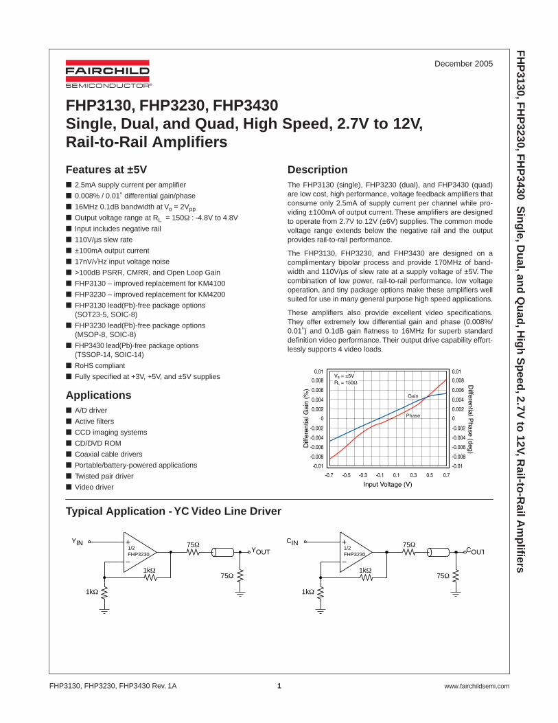
These amplifiers also provide excellent video specifications.They offer extremely low differential gain and phase (0.008%/0.01˚) and 0.1dB gain flatness to 16MHz for superb standarddefinition video performance. Their output drive capability effort-lessly supports 4 video loads.
Typical Application - YC Video Line Driver
YIN
1kΩ
1kΩ
75Ω
75ΩYOUT
1/2 FHP3230
CIN
1kΩ
1kΩ
75Ω
75ΩCOUT
1/2 FHP3230
0.01
Diff
eren
tial G
ain
(%)
-0.7 -0.5 -0.3 -0.1 0.1 0.3 0.5 0.7
Input Voltage (V)
-0.01
-0.006
-0.004
-0.002
0
0.002
0.004
0.006
0.008
-0.008
0.01
Differential P
hase (deg)
-0.01
-0.006
-0.004
-0.002
0
0.002
0.004
0.006
0.008
-0.008
Vs = ±5VRL = 150Ω
Gain
Phase

www.fairchildsemi.com
2
FHP3130, FHP3230, FHP3430 Rev. 1A
FH
P31
30, F
HP
3230
, FH
P34
30
Sin
gle
, Du
al, a
nd
Qu
ad, H
igh
Sp
eed
, 2.7
V t
o 1
2V, R
ail-
to-R
ail A
mp
lifier
s
2
3
4 5
6
7
8
-Vs
+Vs
+IN1
NC
OUT
NC
1
-IN1
NC
FHP3130 SOIC
-+2
3
5
4+IN
+Vs
-IN
1
-Vs
OUT
FHP3130 SOT23
7
2
3
4-Vs
+IN1
1
-IN1
OUT1
FHP3230SOIC/MSOP
5
6
7
8
OUT2
+Vs
-IN2
+IN2
4
2
3
4 11
12
13
14
+Vs
-IN
+IN1
OUT4
+IN4
-Vs
1
-IN1
OUT1
FHP3430 SOIC/TSSOP
5
6
7OUT2
-IN2
+IN2
8
9
10 +IN3
-IN
OUT3
Pin Configurations Pin Assignments
FHP3230
Pin# Pin Type Description
1 OUT1 Output Output, channel 1
2 -IN1 Input Negative Input, channel 1
3 +IN1 Input Positive Input, channel 1
4 -Vs Input Negative supply
5 +IN2 Input Positive Input, channel 2
6 -IN2 Input Negative Input, channel 2
7 OUT2 Output Output, channel 2
8 +Vs Input Positive supply
FHP3130
Pin# SOT/SOIC Pin Type Description
1 / 6 OUT Input Output
2 / 4 -Vs Input Negative supply
3 / 3 +IN Input Positive Input
4 / 4 -IN Input Negative Input
5 / 7 +Vs Input Positive supply
na / 1, 5, 8 NC - No Connect
FHP3430
Pin# Pin Type Description
1 OUT1 Output Output, channel 1
2 -IN1 Input Negative Input, channel 1
3 +IN1 Input Positive Input, channel 1
4 +Vs Input Positive supply
5 +IN2 Input Positive Input, channel 2
6 -IN2 Input Negative Input, channel 2
7 OUT2 Output Output, channel 2
8 OUT3 Output Output, channel 3
9 -IN3 Input Negative Input, channel 3
10 +IN3 Input Positive Input, channel 3
11 -Vs Input Negative supply
12 +IN4 Input Positive Input, channel 4
13 -IN4 Input Negative Input, channel 4
14 OUT4 Output Output, channel 4
FHP3130, FHP3230, FHP3430 Rev. 1A
3
www.fairchildsemi.com
F
HP
3130, FH
P3230, F
HP
3430 Sin
gle, D
ual, an
d Q
uad
, Hig
h S
peed
, 2.7V to
12V, Rail-to
-Rail A
mp
lifiers
Absolute Maximum Ratings
Reliability Information
Note:
1. Package thermal resistance (
θ
JA
), JDEC standard, multi-layer test boards, still air.
ESD Protection
Recommended Operating Conditions
Parameter Min Max Unit
Supply Voltage 0 12.6 V
Input Voltage Range -V
s
-0.5V +V
s
+ 0.5V V
Parameter Min Typ Max Unit
Junction Temperature 150 ˚C
Storage Temperature Range -65 150 ˚C
Lead Temperature (Soldering, 10s) 300 ˚C
8-Lead SOIC
1
155 ˚C/W
8-Lead MSOP
1
246 ˚C/W
5-Lead SOT23
1
296 ˚C/W
14-Lead TSSOP
1
130 ˚C/W
14-Lead SOIC
1
128 ˚C/W
Product FHP3130 FHP3230 FHP3430
Package SOT23 SOIC SOIC MSOP SOIC TSSOP
Human Body Model (HBM) TBD TBD 3.5kV 3.5kV TBD TBD
Charged Device Model (CDM) TBD TBD 2kV 1.5kV TBD TBD
Parameter Min Typ Max Unit
Operating Temperature Range -40 +85 ˚C
Supply Voltage Range 2.7 12 V

www.fairchildsemi.com
4
FHP3130, FHP3230, FHP3430 Rev. 1A
FH
P31
30, F
HP
3230
, FH
P34
30
Sin
gle
, Du
al, a
nd
Qu
ad, H
igh
Sp
eed
, 2.7
V t
o 1
2V, R
ail-
to-R
ail A
mp
lifier
sElectrical Characteristics at +3V
T
c
= 25˚C, V
s
= 3V, R
L
= 2k
Ω
to V
s
/2, G = 2, R
f
= R
g
=1k
Ω
; unless otherwise noted.
Symbol Parameter Conditions Min Typ Max Units
Frequency Domain Response
UGBW -3dB Bandwidth G = +1, V
OUT
= 0.2V
pp
160 MHz
BW
ss
-3dB Bandwidth G = +2, V
OUT
= 0.2V
pp
50 MHz
BW
Ls
Full Power Bandwidth G = +2, V
OUT
= 1V
pp
45 MHz
BW
0.1dBss
0.1dB Bandwidth G = +2, R
L
= 150
Ω
,
R
f
= R
g
= 1.5k
Ω
,V
OUT
= 0.2V
pp
25 MHz
GBWP Gain Bandwitdth Product G = +6,
V
OUT
= 0.2V
pp
60 MHz
Time Domain Response
t
R
, t
F
Rise and Fall Time V
OUT
= 0.2V step 12 ns
t
S
Settling Time to 0.1% V
OUT
= 2V step 45 ns
OS Overshoot V
OUT
= 0.2V step <1 %
SR Slew Rate V
OUT
= 2V step, G = -1 90 V/
µ
s
Distortion / Noise Response
HD2 2nd Harmonic Distortion V
OUT
= 1V
pp
, 5MHz 50 dBc
HD3 3rd Harmonic Distortion V
OUT
= 1V
pp
, 5MHz 50 dBc
THD Total Harmonic Distortion V
OUT
= 2V
pp
, 5MHz, R
L
= 100
Ω
, G = -1 50 dB
e
n
Input Voltage Noise > 100kHz 17 nV/
√
Hz
X
TALK
Crosstalk FHP3230 at 1MHz 62 dB
DC Performance
V
IO
Input Offset Voltage 1 mV
dV
IO
Average Drift -5
µ
V/˚C
I
b
Input Bias Current -1.8
µ
A
dI
b
Average Drift -3.5 nA/˚C
I
IO
Input Offset Current 0.01
µ
A
PSRR Power Supply Rejection Ratio DC 100 dB
A
OL
Open Loop Gain DC, R
L
= 150
Ω
100 dB
I
S
Supply Current per Amplifier 2.5 mA
Input Characteristics
R
IN
Input Resistance 500 k
Ω
C
IN
Input Capacitance 1.25 pF
CMIR Input Common Mode V Range -0.3 to 2 V
CMRR Common Mode Rejection Ratio DC, V
CM
= 0V to V
s - 1.5 95 dB
Output Characteristics
VO Output Voltage Swing
RL = 2kΩ to Vs/2, G = -1 0.05 to 2.95
V
RL = 150Ω to Vs/2, G = -1 0.1 to 2.9 V
IOUT Linear Output Current ±100 mA
ISC Short Circuit Output Current VO = Vs/2 ±120 mA

FHP3130, FHP3230, FHP3430 Rev. 1A 5 www.fairchildsemi.com
FH
P3130, F
HP
3230, FH
P3430 S
ing
le, Du
al, and
Qu
ad, H
igh
Sp
eed, 2.7V
to 12V, R
ail-to-R
ail Am
plifi
ers
Electrical Characteristics at +5VTc = 25˚C, Vs = 5V, RL = 2kΩ to Vs/2, G = 2, Rf = Rg =1kΩ; unless otherwise noted.
Symbol Parameter Conditions Min Typ Max UnitsFrequency Domain Response
UGBW -3dB Bandwidth G = +1, VOUT = 0.2Vpp 165 MHz
BWss -3dB Bandwidth G = +2, VOUT = 0.2Vpp 50 MHz
BWLs Full Power Bandwidth G = +2, VOUT = 2Vpp 30 MHz
BW0.1dBss 0.1dB Bandwidth G = +2, RL = 150Ω, Rf = Rg = 1.5kΩ,VOUT = 0.2Vpp
18 MHz
GBWP Gain Bandwitdth Product G = +6, VOUT = 0.2Vpp 60 MHz
Time Domain Response
tR, tF Rise and Fall Time VOUT = 0.2V step 12 ns
tS Settling Time to 0.1% VOUT = 2V step 55 ns
OS Overshoot VOUT = 0.2V step <1 %
SR Slew Rate VOUT = 2V step, G = -1 105 V/µs
Distortion / Noise Response
HD2 2nd Harmonic Distortion VOUT = 2Vpp, 5MHz 56 dBc
HD3 3rd Harmonic Distortion VOUT = 2Vpp, 5MHz 75 dBc
THD Total Harmonic Distortion VOUT = 2Vpp, 5MHz 56 dB
en Input Voltage Noise > 100kHz 17 nV/√Hz
XTALK Crosstalk FHP3230 at 1MHz 62 dB
DG Differential Gain NTSC (3.58MHz), RL = 150Ω, AC coupled into 220µF, Vs = ±2.5V
0.02 %
DP Differential Phase NTSC (3.58MHz), RL = 150Ω, AC coupled into 220µF, Vs = ±2.5V
0.04 ˚
DC Performance
VIO Input Offset Voltage 1 mV
dVIO Average Drift -5 µV/˚C
Ib Input Bias Current -1.8 µA
dIb Average Drift -3.5 nA/˚C
IIO Input Offset Current 0.01 µA
PSRR Power Supply Rejection Ratio DC 100 dB
AOL Open Loop Gain DC, RL = 150Ω 100 dB
IS Supply Current per Amplifier 2.5 mA
Input Characteristics
RIN Input Resistance 500 kΩ
CIN Input Capacitance 1.2 pF
CMIR Input Common Mode V Range -0.3 to 4 V
CMRR Common Mode Rejection Ratio DC, VCM = 0V to Vs - 1.5 95 dB
Output Characteristics
VO Output Voltage Swing
RL = 2kΩ to Vs/2 0.05 to 4.95
V
RL = 150Ω to Vs/2 0.1 to 4.9 V
IOUT Linear Output Current ±100 mA
ISC Short Circuit Output Current VO = Vs/2 ±120 mA

www.fairchildsemi.com 6 FHP3130, FHP3230, FHP3430 Rev. 1A
FH
P31
30, F
HP
3230
, FH
P34
30
Sin
gle
, Du
al, a
nd
Qu
ad, H
igh
Sp
eed
, 2.7
V t
o 1
2V, R
ail-
to-R
ail A
mp
lifier
sElectrical Characteristics at ±5VTc = 25˚C, Vs = ±5V, RL = 2kΩ to GND, G = 2, Rf = Rg =1kΩ; unless otherwise noted.
Notes:
1. 100% tested at 25˚C
2. Min/max guaranteed by design/characterization.
Symbol Parameter Conditions Min Typ Max UnitsFrequency Domain Response
UGBW -3dB Bandwidth G = +1, VOUT = 0.2Vpp 170 MHz
BWss -3dB Bandwidth G = +2, VOUT = 0.2Vpp 50 MHz
BWLs Full Power Bandwidth G = +2, VOUT = 2Vpp 30 MHz
BW0.1dBss 0.1dB Bandwidth G = +2, RL = 150Ω, Rf = Rg = 1.5kΩ,VOUT = 0.2Vpp
16 MHz
GBWP Gain Bandwitdth Product G = +6, VOUT = 0.2Vpp 60 MHz
Time Domain Response
tR, tF Rise and Fall Time VOUT = 0.2V step 12 ns
tS Settling Time to 0.1% VOUT = 2V step 52 ns
OS Overshoot VOUT = 0.2V step <1 %
SR Slew Rate VOUT = 2V step, G = -1 110 V/µs
Distortion / Noise Response
HD2 2nd Harmonic Distortion VOUT = 2Vpp, 5MHz 55 dBc
HD3 3rd Harmonic Distortion VOUT = 2Vpp, 5MHz 75 dBc
THD Total Harmonic Distortion VOUT = 2Vpp, 5MHz 55 dB
en Input Voltage Noise > 100kHz 17 nV/√Hz
XTALK Crosstalk FHP3230 at 1MHz 62 dB
DG Differential Gain NTSC (3.58MHz), RL = 150Ω, AC coupled into 220µF
0.008 %
DP Differential Phase NTSC (3.58MHz), RL = 150Ω, AC coupled into 220µF
0.01 ˚
DC Performance
VIO Input Offset Voltage1 -6 1 6 mV
dVIO Average Drift -5 µV/˚C
Ib Input Bias Current1 -3.5 -1.8 µA
dIb Average Drift -3.5 nA/˚C
IIO Input Offset Current1 -0.8 0.002 0.8 µA
PSRR Power Supply Rejection Ratio2 DC 80 100 dB
AOL Open Loop Gain2 DC, RL = 150Ω 80 100 dB
IS Supply Current per Amplifier1 2.5 3.5 mA
Input Characteristics
RIN Input Resistance 500 kΩ
CIN Input Capacitance 1.1 pF
CMIR Input Common Mode V Range -5 to 4 V
CMRR Common Mode Rejection Ratio2 DC, VCM = -5V to 3.5V 75 100 dB
Output Characteristics
VO Output Voltage Swing
RL = 2kΩ -4.95 to 4.95
V
RL = 150Ω1 -4.65 -4.8 to 4.8 4.65 V
IOUT Linear Output Current ±100 mA
ISC Short Circuit Output Current VO = 0V ±120 mA

FHP3130, FHP3230, FHP3430 Rev. 1A 7 www.fairchildsemi.com
FH
P3130, F
HP
3230, FH
P3430 S
ing
le, Du
al, and
Qu
ad, H
igh
Sp
eed, 2.7V
to 12V, R
ail-to-R
ail Am
plifi
ers
Typical Performance CharacteristicsTc = 25˚C, Vs = 5V, RL = 2kΩ to Vs/2 for Vs = 5V and 3V, RL = 2kΩ to ground for Vs = ±5V, G = 2, Rf = Rg = 1kΩ; unless otherwise noted.
1
Nor
mal
ized
Gai
n (d
B)
0.1
Frequency (MHz)
0
-1
-2
-3
-4
-5
-6
-7
1000100101
G = 10
G = 1Rf = 0
G = 5
G = 2
Vs = ±5VVo = 0.2Vpp
1
Nor
mal
ized
Gai
n (d
B)
0.1
Frequency (MHz)
0
-1
-2
-3
-4
-5
-6
-7
1000100101
G = -1
Vs = ±5VVo = 0.2Vpp
G = -10
G = -5
G = -2
-30
-40
-50
-60
-70
-80
PS
RR
(dB
)
0.1 1 10 30
Frequency (MHz)
-90
-20
-30
-40
-50
-60
-70
-80
PS
RR
(dB
)
0.1 1 10 30
Frequency (MHz)
-90
Using 0.1µF and 0.01µF Bypass Capacitors as suggested
1
Nor
mal
ized
Gai
n (d
B)
0.1
Frequency (MHz)
0
-1
-2
-3
-4
-5
-6
-7
1000100101
G = 10
G = 1Rf = 0
G = 5
G = 2
Vs = +5VVo = 0.2Vpp
1N
orm
aliz
ed G
ain
(dB
)
0.1
Frequency (MHz)
0
-1
-2
-3
-4
-5
-6
-7
1000100101
G = -1
Vs = +5VVo = 0.2Vpp
G = -10
G = -5
G = -2
1
Nor
mal
ized
Gai
n (d
B)
0.1
Frequency (MHz)
0
-1
-2
-3
-4
-5
-6
-7
1000100101
G = 10
G = 1Rf = 0
G = 5
G = 2
Vs = +3VVo = 0.2Vpp
1
Nor
mal
ized
Gai
n (d
B)
0.1
Frequency (MHz)
0
-1
-2
-3
-4
-5
-6
-7
1000100101
G = -1
Vs = +3VVo = 0.2Vpp
G = -10
G = -5
G = -2
Figure 5. Non-Inverting Freq. Response (+3V) Figure 6. Inverting Freq. Response (+3V)
Figure 3. Non-Inverting Freq. Response (+5V) Figure 4. Inverting Freq. Response (+5V)
Figure 1. Non-Inverting Freq. Response (±5V) Figure 2. Inverting Freq. Response (±5V)

www.fairchildsemi.com 8 FHP3130, FHP3230, FHP3430 Rev. 1A
FH
P31
30, F
HP
3230
, FH
P34
30
Sin
gle
, Du
al, a
nd
Qu
ad, H
igh
Sp
eed
, 2.7
V t
o 1
2V, R
ail-
to-R
ail A
mp
lifier
sTypical Performance CharacteristicsTc = 25˚C, Vs = 5V, RL = 2kΩ to Vs/2 for Vs = 5V and 3V, RL = 2kΩ to ground for Vs = ±5V, G = 2, Rf = Rg = 1kΩ; unless otherwise noted.
1
Nor
mal
ized
Gai
n (d
B)
0.1
Frequency (MHz)
0
-1
-2
-3
-4
-5
-6
-7
1000100101
CL = 2000pFRS = 5Ω
Vs = +3VVo = 0.2Vpp
1
Nor
mal
ized
Gai
n (d
B)
0.1
Frequency (MHz)
0
-1
-2
-3
-4
-5
-6
-7
1000100101
RL = 50Ω
Vs = +3VVo = 0.2Vpp
RL = 5KΩ
RL = 1KΩ
RL = 150Ω
CL = 1000pFRS = 6.5Ω
CL = 500pFRS = 10Ω
CL = 100pFRS = 20Ω
CL = 50pFRS = 15Ω
+
-1kΩ
1kΩ
Rs
CL RL
1
Nor
mal
ized
Gai
n (d
B)
0.1
Frequency (MHz)
0
-1
-2
-3
-4
-5
-6
-7
1000100101
VO = 1Vpp
VO = 2Vpp
VO = 4Vpp
0.2
0
-0.2
-0.4
-0.6
-0.8Nor
mal
ized
Gai
n (d
B)
0.1
Frequency (MHz)
-1
100101
G = 2Vs = +5V
Vs = 3V
Vs = 5V
Vs = 10V
G = 2Rf = Rg = 1.5kΩVs = +5VRL = 150Ω
-40
Dis
tort
ion
(dB
c)
0.1
Frequency (MHz)
-45
-50
-55
-60
-65
-70
-75
-80
-85
-90
101
RL = 1KΩ
VO = 1Vpp
RL = 5KΩ
RL = 2KΩ
RL = 150Ω
-40
Dis
tort
ion
(dB
c)
0.1
Frequency (MHz)
-45
-50
-55
-60
-65
-70
-75
-80
-85
-90
101
RL = 1KΩ
VO = 1Vpp
RL = 5KΩ
RL = 2KΩ
RL = 150Ω
Figure 11. HD2 vs. RL (+3V) Figure 12. HD3 vs. RL (+3V)
Figure 7. Frequency Response vs. CL (+3V) Figure 8. Frequency Response vs. RL (+3V)
Figure 9. Large Signal Freq. Response (+5V) Figure 10. Gain vs. Flattness

FHP3130, FHP3230, FHP3430 Rev. 1A 9 www.fairchildsemi.com
FH
P3130, F
HP
3230, FH
P3430 S
ing
le, Du
al, and
Qu
ad, H
igh
Sp
eed, 2.7V
to 12V, R
ail-to-R
ail Am
plifi
ers
Typical Performance CharacteristicsTc = 25˚C, Vs = 5V, RL = 2kΩ to Vs/2 for Vs = 5V and 3V, RL = 2kΩ to ground for Vs = ±5V, G = 2, Rf = Rg = 1kΩ; unless otherwise noted.
0
-10
-20
-30
-40
-50
-60
-70
-80
PS
RR
(dB
)
10k
Frequency (Hz)
-90
1G100k 1M 10M 100M
Vs = ±5V
-20
-30
-40
-50
-60
-70
-80
-90
-100
CM
RR
(dB
)
10k
Frequency (Hz)
-120
1G100k 1M 10M 100M
Vs = ±5V
3.25
Out
put V
olta
ge (
V)
-2.0
Input Voltage (V)
3.02.752.502.252.0
1.751.501.251.0
0.750.500.25
0-0.25
-1.5 -1.0 -0.5 0 0.5 1.0 1.5 2.0
RL = 10KΩ
RL = 150Ω
G = -1
RL = 75Ω
80
70
60
50
40
30
20
10
0
-10
Gai
n (d
B)
10k
Frequency (Hz)
-20
1G100k 1M 10M 100M
Phase (deg)
0
-20
-40
-60
-80
-100
-120
-140
-160
-180
-200
Gain
Phase
Vs = ±5V
-40
Dis
tort
ion
(dB
c)
0.5
Output Amplitude (Vpp)
-95
2.50.9 1.3 1.7 2.1 2.30.7 1.1 1.5 1.9
-40
Dis
tort
ion
(dB
c)
0.5
Output Amplitude (Vpp)
-45
-50
-55
-60
-65
-70
-75
-80
-85
-90
-45
-50
-55
-60
-65
-70
-75
-80
-85
-90
-95
0.7 0.9 1.1 1.3 1.5 1.7 1.9 2.1 2.3 2.5
10MHz
5MHz
1MHz
100KHz
10MHz
5MHz
100MHz
1MHz
Figure 17. Open Loop Gain and Phase Figure 18. Output Swing vs. Load (+3V)
Figure 15. CMRR vs. Frequency Figure 16. PSRR vs. Frequency
Figure 13. HD2 vs. VO (+5V) Figure 14. HD3 vs. VO (+5V)

www.fairchildsemi.com 10 FHP3130, FHP3230, FHP3430 Rev. 1A
FH
P31
30, F
HP
3230
, FH
P34
30
Sin
gle
, Du
al, a
nd
Qu
ad, H
igh
Sp
eed
, 2.7
V t
o 1
2V, R
ail-
to-R
ail A
mp
lifier
sTypical Performance CharacteristicsTc = 25˚C, Vs = 5V, RL = 2kΩ to Vs/2 for Vs = 5V and 3V, RL = 2kΩ to ground for Vs = ±5V, G = 2, Rf = Rg = 1kΩ; unless otherwise noted.
-30
Cro
ssta
lk (
dB)
0.1
Frequency (MHz)
-35-40-45-50-55-60-65-70-75-80-85-90
1 10 100
100
90
80
70
60
50
40
30
20
10Inpu
t Vol
tage
Noi
se (
nV/√
Hz)
0.0001
Frequency (MHz)
0
1000.001 0.01 0.1 1 10
2.5
2.0
1.5
1.0
0.5
0
Vol
tage
(V
)
0
Time (µs)
-0.5
1.0
G = 2
0.1 0.2 0.3 0.4 0.5 0.6 0.7 0.8 0.9
Out
put V
olta
ge (
0.5V
/div
)
Time (0.2µs/div)
1.2V Offset
0.6V Offset
No Offset
-0.6V Offset
-1.2V Offset
G = -1
Figure 20. Crosstalk vs. Frequency (+3V) Figure 19. Input Voltage Noise (+3V)
Figure 21. Pulse Resp. vs. Common Mode Voltage Figure 22. Large Signal Pulse Response (+3V)
Figure 23. Large Signal Pulse Response (+5V) Figure 24. Large Signal Pulse Response (±5V)
4.5
4.0
3.5
3.0
2.5
2.0
1.5
1.0
0.5
0
Vol
tage
(V
)
0
Time (µs)
-0.5
1.00.1 0.2 0.3 0.4 0.5 0.6 0.7 0.8 0.9
G = 2
3.5
3.0
1.5
2.0
2.5
1.0
0.5
0
Vol
tage
(V
)
0
Time (µs)
-0.5
1.00.1 0.2 0.3 0.4 0.5 0.6 0.7 0.8 0.9
G = 2

FHP3130, FHP3230, FHP3430 Rev. 1A 11 www.fairchildsemi.com
FH
P3130, F
HP
3230, FH
P3430 S
ing
le, Du
al, and
Qu
ad, H
igh
Sp
eed, 2.7V
to 12V, R
ail-to-R
ail Am
plifi
ers
Typical Performance CharacteristicsTc = 25˚C, Vs = 5V, RL = 2kΩ to Vs/2 for Vs = 5V and 3V, RL = 2kΩ to ground for Vs = ±5V, G = 2, Rf = Rg = 1kΩ; unless otherwise noted.
0.05
0.04
0.03
0.02
0.01
0
-0.01
-0.02
-0.03
Diff
eren
tial G
ain
(%)
-0.6 -0.4 -0.2 0 0.2 0.4 0.6
Input Voltage (V)
-0.04
RL = 150ΩAC coupled into 220µF
Gain
Phase
0.05
0.04
0.03
0.02
0.01
0
-0.01
-0.02
-0.03
Differential P
hase (deg)
-0.04
0.01
Diff
eren
tial G
ain
(%)
-0.7 -0.5 -0.3 -0.1 0.1 0.3 0.5 0.7
Input Voltage (V)
-0.01
-0.006
-0.004
-0.002
0
0.002
0.004
0.006
0.008
-0.008
0.01
Differential P
hase (deg)
-0.01
-0.006
-0.004
-0.002
0
0.002
0.004
0.006
0.008
-0.008
Vs = ±5VRL = 150ΩAC coupled into 220µF
Gain
Phase
Figure 26. Differential Gain and Phase (±5V) Figure 25. Differential Gain and Phase (±2.5V)
www.fairchildsemi.com 12 FHP3130, FHP3230, FHP3430 Rev. 1A
FH
P31
30, F
HP
3230
, FH
P34
30
Sin
gle
, Du
al, a
nd
Qu
ad, H
igh
Sp
eed
, 2.7
V t
o 1
2V, R
ail-
to-R
ail A
mp
lifier
sApplications Information
General DescriptionThe FHP3130 (single), FHP3230 (dual), and FHP3430 (quad)are low cost, high performance, voltage feedback amplifiers thatconsume only 2.5mA of supply current per channel while pro-viding ±100mA of output current. These amplifiers are designedto operate from 2.7V to 12V (±6V) supplies. The common modevoltage range extends below the negative rail and the outputprovides rail-to-rail performance.
The FHP3130, FHP3230, and FHP3430 are designed on acomplimentary bipolar process and provide 170MHz of band-width and 110V/µs of slew rate at a supply voltage of ±5V. Thecombination of low power, rail-to-rail performance, low voltageoperation, and tiny package options make these amplifiers wellsuited for use in many general purpose high speed applications.
These amplifiers also provide excellent video specifications.They offer extremely low differential gain and phase (0.008%/0.01˚) and 0.1dB gain flatness to 16MHz for superb standarddefinition video performance. Their output drive capability effort-lessly supports 4 video loads.
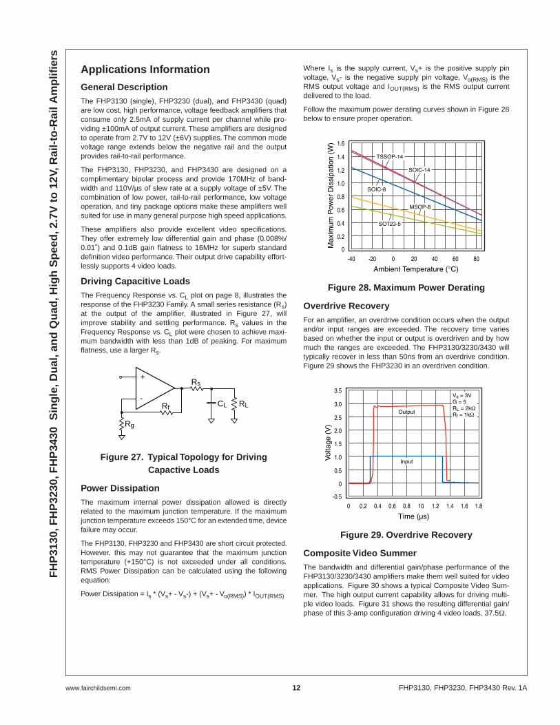
Driving Capacitive LoadsThe Frequency Response vs. CL plot on page 8, illustrates theresponse of the FHP3230 Family. A small series resistance (Rs)at the output of the amplifier, illustrated in Figure 27, willimprove stability and settling performance. Rs values in theFrequency Response vs. CL plot were chosen to achieve maxi-mum bandwidth with less than 1dB of peaking. For maximumflatness, use a larger Rs.
Figure 27. Typical Topology for Driving Capactive Loads
Power Dissipation The maximum internal power dissipation allowed is directlyrelated to the maximum junction temperature. If the maximumjunction temperature exceeds 150°C for an extended time, devicefailure may occur.
The FHP3130, FHP3230 and FHP3430 are short circuit protected.However, this may not guarantee that the maximum junctiontemperature (+150°C) is not exceeded under all conditions.RMS Power Dissipation can be calculated using the followingequation:
Power Dissipation = Is * (Vs+ - Vs-) + (Vs+ - Vo(RMS)) * IOUT(RMS)
Where Is is the supply current, Vs+ is the positive supply pinvoltage, Vs- is the negative supply pin voltage, Vo(RMS) is theRMS output voltage and IOUT(RMS) is the RMS output currentdelivered to the load.
Follow the maximum power derating curves shown in Figure 28below to ensure proper operation.
Figure 28. Maximum Power Derating
Overdrive Recovery For an amplifier, an overdrive condition occurs when the outputand/or input ranges are exceeded. The recovery time variesbased on whether the input or output is overdriven and by howmuch the ranges are exceeded. The FHP3130/3230/3430 willtypically recover in less than 50ns from an overdrive condition.Figure 29 shows the FHP3230 in an overdriven condition.
Figure 29. Overdrive Recovery
Composite Video Summer The bandwidth and differential gain/phase performance of theFHP3130/3230/3430 amplifiers make them well suited for videoapplications. Figure 30 shows a typical Composite Video Sum-mer. The high output current capability allows for driving multi-ple video loads. Figure 31 shows the resulting differential gain/phase of this 3-amp configuration driving 4 video loads, 37.5Ω.
+
-Rf
Rg
Rs
CL RL
1.6
1.4
1.2
1.0
0.8
0.6
0.4
0.2
Max
imum
Pow
er D
issi
patio
n (W
)
-40
Ambient Temperature (°C)
0
-20 0 20 40 60 80
TSSOP-14
SOIC-14
SOIC-8
MSOP-8
SOT23-5
3.5
3.0
2.5
2.0
1.5
1.0
0.5
0
Vol
tage
(V
)
0
Time (µs)
-0.5
0.2 0.60.4 0.8 10 1.2 1.4 1.6 1.8
Output
Input
Vs = 3VG = 5RL = 2kΩRf = 1kΩ
FHP3130, FHP3230, FHP3430 Rev. 1A 13 www.fairchildsemi.com
FH
P3130, F
HP
3230, FH
P3430 S
ing
le, Du
al, and
Qu
ad, H
igh
Sp
eed, 2.7V
to 12V, R
ail-to-R
ail Am
plifi
ers
Figure 30. Typical Composite Video Summer
Figure 31. DG/DP of CV Summer Driving 4 Video Loads
Layout ConsiderationsGeneral layout and supply bypassing play major roles in highfrequency performance. Fairchild has evaluation boards to useas a guide for high frequency layout and as aid in device testingand characterization. Follow the steps below as a basis for highfrequency layout:
• Include 6.8µF and 0.01µF ceramic capacitors
• Place the 6.8µF capacitor within 0.75 inches of the power pin
• Place the 0.01µF capacitor within 0.1 inches of the power pin
• Remove the ground plane under and around the part, especially near the input and output pins to reduce parasiticcapacitance
• Minimize all trace lengths to reduce series inductances
Refer to the evaluation board layouts shown below for moreinformation.
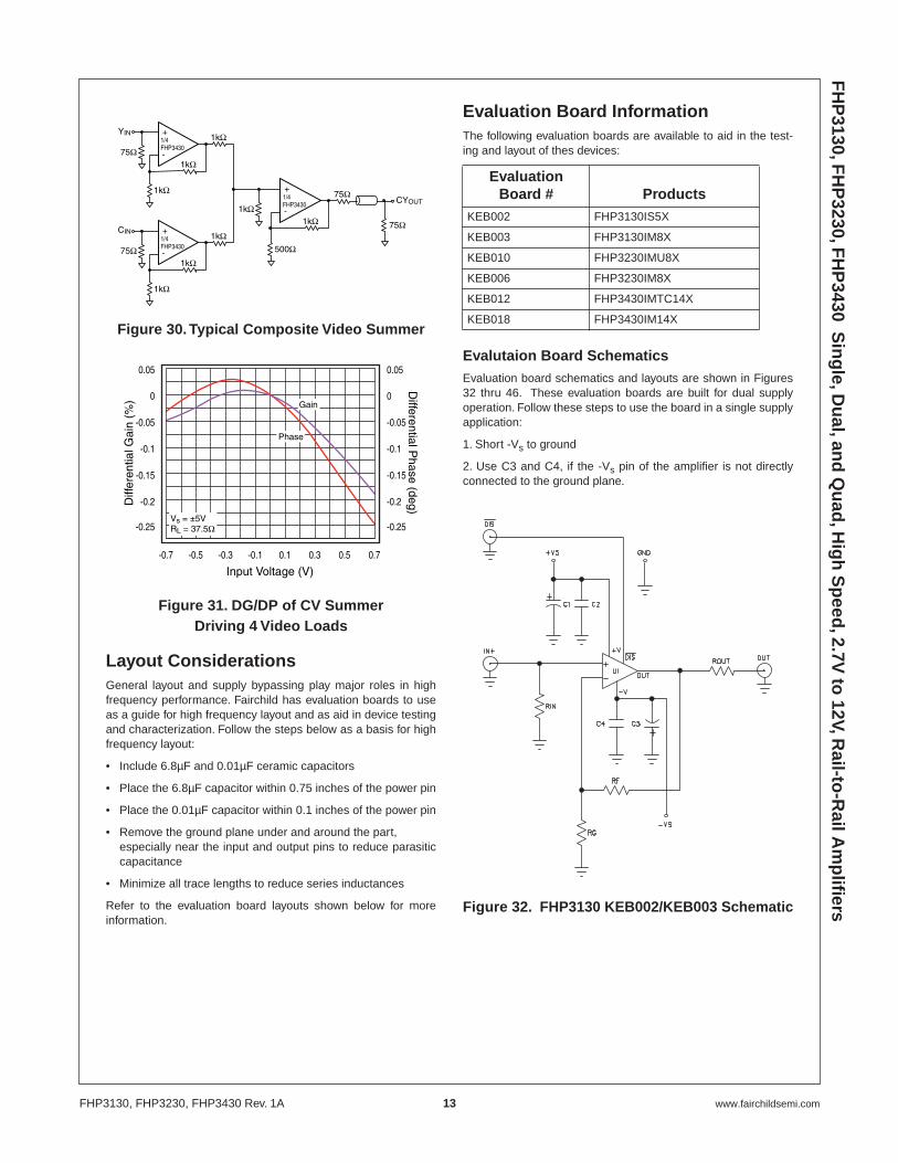
Evaluation Board InformationThe following evaluation boards are available to aid in the test-ing and layout of thes devices:
Evalutaion Board SchematicsEvaluation board schematics and layouts are shown in Figures32 thru 46. These evaluation boards are built for dual supplyoperation. Follow these steps to use the board in a single supplyapplication:
1. Short -Vs to ground
2. Use C3 and C4, if the -Vs pin of the amplifier is not directlyconnected to the ground plane.
Figure 32. FHP3130 KEB002/KEB003 Schematic
+
-1kΩ
1kΩ
1kΩYIN
75Ω
75Ω
1/4FHP3430
+
-1kΩ
1kΩ
1kΩCIN
75Ω1/4FHP3430
+
-1kΩ
500Ω
1kΩ1/4FHP3430
CYOUT75Ω
0.05
0
-0.05
-0.1
-0.15
-0.2
-0.25
Diff
eren
tial G
ain
(%)
0.05
0
-0.05
-0.1
-0.15
-0.2
-0.25
Differential P
hase (deg)
-0.7
Input Voltage (V)-0.5 -0.3 -0.1 0.1 0.3 0.5 0.7
Gain
Phase
Vs = ±5VRL = 37.5Ω
Evaluation Board # Products
KEB002 FHP3130IS5X
KEB003 FHP3130IM8X
KEB010 FHP3230IMU8X
KEB006 FHP3230IM8X
KEB012 FHP3430IMTC14X
KEB018 FHP3430IM14X
www.fairchildsemi.com 14 FHP3130, FHP3230, FHP3430 Rev. 1A
FH
P31
30, F
HP
3230
, FH
P34
30
Sin
gle
, Du
al, a
nd
Qu
ad, H
igh
Sp
eed
, 2.7
V t
o 1
2V, R
ail-
to-R
ail A
mp
lifier
s
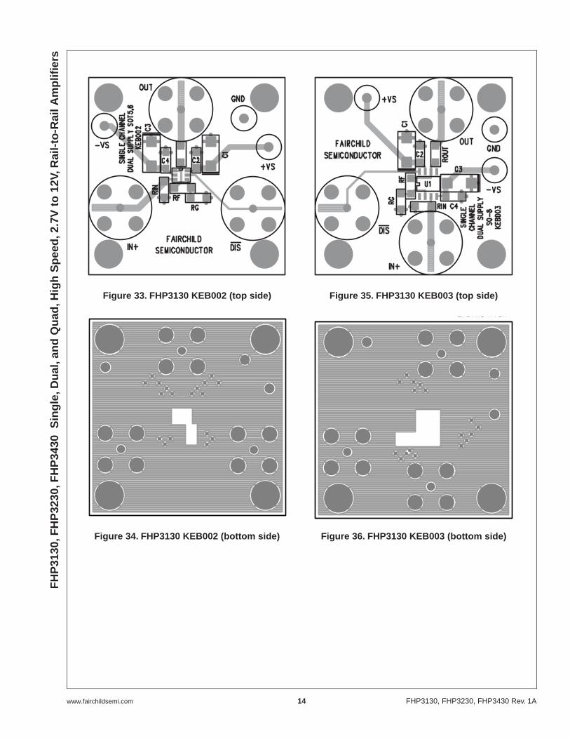
Figure 33. FHP3130 KEB002 (top side)
Figure 34. FHP3130 KEB002 (bottom side)
Figure 35. FHP3130 KEB003 (top side)
Figure 36. FHP3130 KEB003 (bottom side)

FHP3130, FHP3230, FHP3430 Rev. 1A 15 www.fairchildsemi.com
FH
P3130, F
HP
3230, FH
P3430 S
ing
le, Du
al, and
Qu
ad, H
igh
Sp
eed, 2.7V
to 12V, R
ail-to-R
ail Am
plifi
ers
Figure 37. FHP3230 KEB006/KEB010 Schematic
Figure 38. FHP3230 KEB006 (top side)
Figure 39. FHP3230 KEB006 (bottom side)
Figure 40. FHP3230 KEB010 (top side)
www.fairchildsemi.com 16 FHP3130, FHP3230, FHP3430 Rev. 1A
FH
P31
30, F
HP
3230
, FH
P34
30
Sin
gle
, Du
al, a
nd
Qu
ad, H
igh
Sp
eed
, 2.7
V t
o 1
2V, R
ail-
to-R
ail A
mp
lifier
s
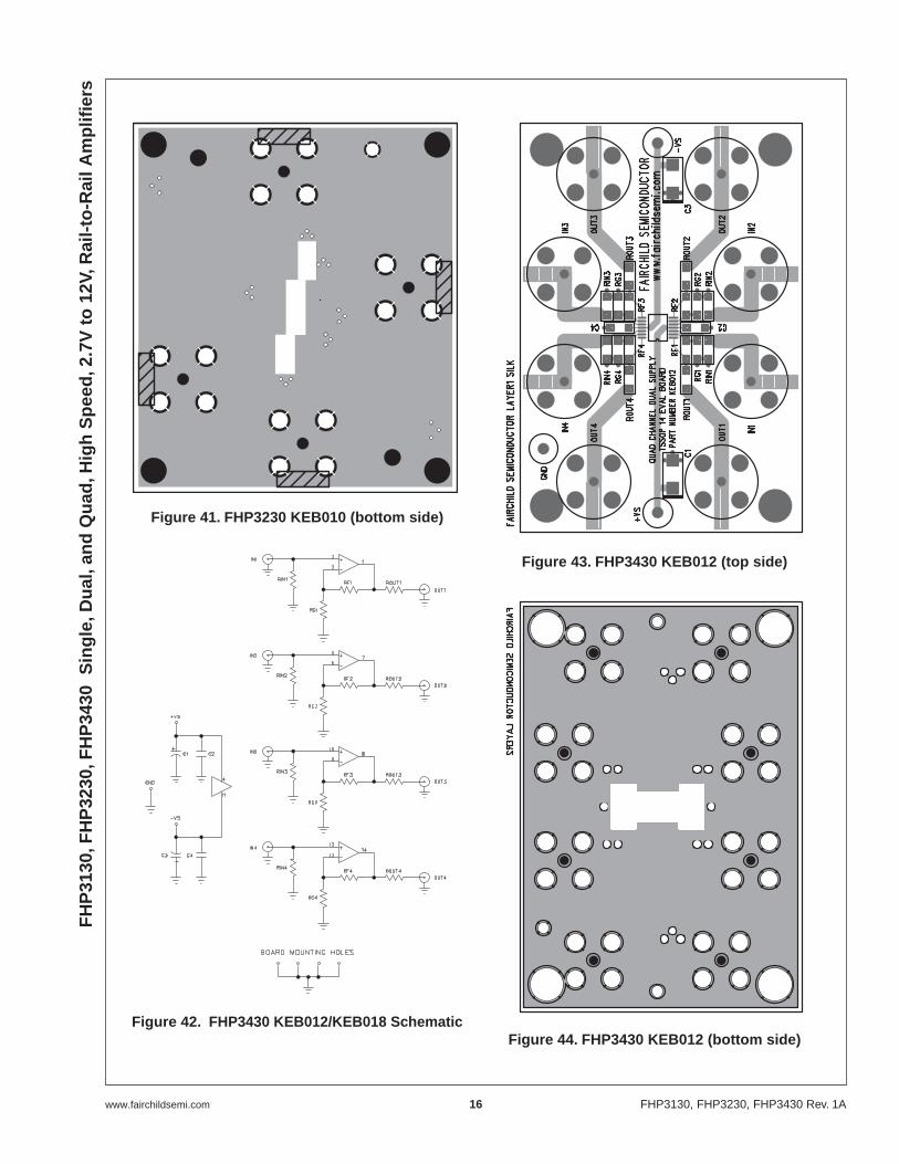
Figure 41. FHP3230 KEB010 (bottom side)
Figure 42. FHP3430 KEB012/KEB018 Schematic
Figure 43. FHP3430 KEB012 (top side)
Figure 44. FHP3430 KEB012 (bottom side)
FHP3130, FHP3230, FHP3430 Rev. 1A 17 www.fairchildsemi.com
FH
P3130, F
HP
3230, FH
P3430 S
ing
le, Du
al, and
Qu
ad, H
igh
Sp
eed, 2.7V
to 12V, R
ail-to-R
ail Am
plifi
ers
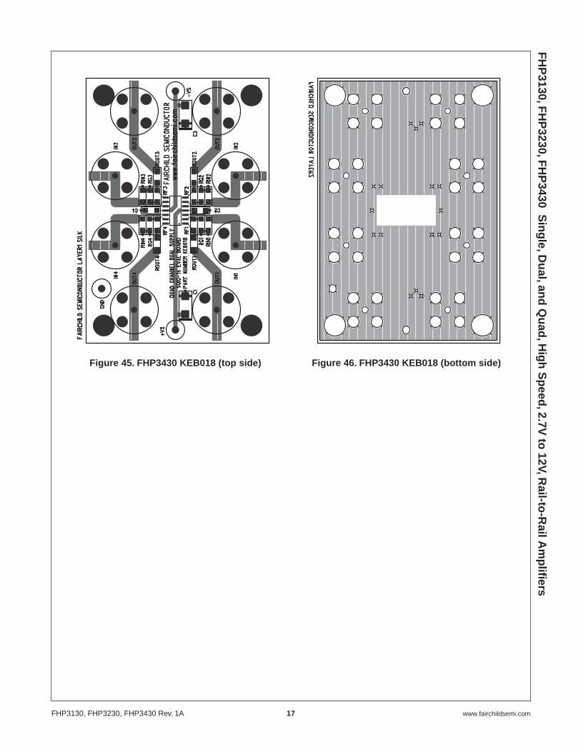
Figure 45. FHP3430 KEB018 (top side) Figure 46. FHP3430 KEB018 (bottom side)

www.fairchildsemi.com 18 FHP3130, FHP3230, FHP3430 Rev. 1A
FH
P31
30, F
HP
3230
, FH
P34
30
Sin
gle
, Du
al, a
nd
Qu
ad, H
igh
Sp
eed
, 2.7
V t
o 1
2V, R
ail-
to-R
ail A
mp
lifier
sMechanical Dimensions
8-Lead Outline Package (SOIC)
8-Lead Outline Package (MSOP)
HECL
ZDCL
e
D
Pin No. 1 B
A A1 A2
7
LDETAIL-A
DETAIL-A
C
h x 45
α
NOTE: 1. All dimensions are in millimeters. 2. Lead coplanarity should be 0 to 0.10mm (.004") max. 3. Package surface finishing: (2.1) Top: matte (charmilles #18~30). (2.2) All sides: matte (charmilles #18~30). (2.3) Bottom: smooth or matte (charmilles #18~30). 4. All dimensions excluding mold flashes and end flash from the package body shall not exceed 0.152mm (.006) per side (D).
SYMBOL MIN MAX A1 0.10 0.25 B 0.36 0.46 C 0.19 0.25 D 4.80 4.98 E 3.81 3.99 e 1.27 BSC H 5.80 6.20 h 0.25 0.50 L 0.41 1.27 A 1.52 1.72 0° ZD 0.53 ref A2 1.37 1.57
8°
SOIC-8
e S
E/2 2X
E3E4
1 2 ccc A B C
– B – 2
3 7
264
D2 A2
A
A1
– A –
– C –
bbb A B CM
b
D43
aaa A
E1
– H –
t1
t2
GaugePlane
0.25mm
R1
R
L
L1
03
02
01
Detail AScale 40:1
Section A - A
b
c c1
b1E2
E1
E
Detail A
5
A
A
SYMBOL MIN MAX A 1.10 A1 0.10 0.05 A2 0.86 0.08 D 3.00 0.10 D2 2.95 0.10 E 4.90 0.15 E1 3.00 0.10 E2 2.95 0.10 E3 0.51 0.13 E4 0.51 0.13 R 0.15 +0.15/-0.06 R1 0.15 +0.15/-0.06 t1 0.31 0.08 t2 0.41 0.08 b 0.33 +0.07/-0.08 b1 0.30 0.05 c 0.18 0.05 c1 0.15 +0.03/-0.02 01 3.0 3.0 02 12.0 3.0 03 12.0 3.0 L 0.55 0.15 L1 0.95 BSC – aaa 0.10 – bbb 0.08 – ccc 0.25 – e 0.65 BSC – S 0.525 BSC –
MSOP-8
–
NOTE: 1 All dimensions are in millimeters (angle in degrees), unless otherwise specified.
2 Datums – B – and – C – to be determined at datum plane – H – .
3 Dimensions "D" and "E1" are to be determined at datum – H – .
4 Dimensions "D2" and "E2" are for top package and dimensions "D" and "E1" are for bottom package.
5 Cross sections A – A to be determined at 0.13 to 0.25mm from the leadtip.
6 Dimension "D" and "D2" does not include mold flash, protrusion or gate burrs.
7 Dimension "E1" and "E2" does not include interlead flash or protrusion.

FHP3130, FHP3230, FHP3430 Rev. 1A 19 www.fairchildsemi.com
FH
P3130, F
HP
3230, FH
P3430 S
ing
le, Du
al, and
Qu
ad, H
igh
Sp
eed, 2.7V
to 12V, R
ail-to-R
ail Am
plifi
ers
Mechanical Dimensions
14-Lead Outline Package (SOIC)
14-Lead Outline Package (TSSOP)
HECL
ZDCL
e
D
Pin No. 1 B
A A1 A2
7°
LDETAIL-A
DETAIL-A
C
h x 45°
α
NOTE: 1. All dimensions are in inches. 2. Lead coplanarity should be 0 to 0.10mm (.004") m 3. Package surface finishing: (2.1) Top: matte (charmilles #18~30). (2.2) All sides: matte (charmilles #18~30). (2.3) Bottom: smooth or matte (charmilles #18~30 4. All dimensions excluding mold flashes and end fla from the package body shall not exceed o.152mm per side (d).
SYMBOL MIN MAX A1 .0040 .0098 B .014 .018 C .0075 .0098 D .337 .344 E .150 .157 e .050 BSC H .2284 .2440 h .0099 .0196 L .016 .050 A .060 .068 0 ZD 0.20 ref A2 .054 .062
8
SOIC-14
E/22X
ddd C B A
6
6
1.0
1.0
1 2 3
9e /2
E1 E
eN
8
– B – 7
2XN/2 TIPS
1.0 DIA
– A –7
– C –
aaa C
ccc
8 3D
C B Abbb M
b NX A1
A2
A
c1c
(b)
b1
5
SECTION AA
10
A
A
– H –
GAGEPLANE
0.25
(0.20)(02)
R1
R
01
(L1)
L(03)
NOTES: 1 All dimensions are in millimeters (angle in degrees).
2 Dimensioning and tolerancing per ASME Y14.5–1994.
3 Dimensions "D" does not include mold flash, protusions or gate burrs. Mold flash protusions or gate burrs shall not exceed 0.15 per side .
4 Dimension "E1" does not include interlead flash or protusion. Interlead flash or protusion shall not exceed 0.25 per side.
5 Dimension "b" does not include dambar protusion. Allowable dambar protusion shall be 0.08mm total in excess of the "b" dimension at maximum material condition. Dambar connot be located on the lower radius of the foot. Minimum space between protusion and adjacent lead is 0.07mm for 0.5mm pitch packages.
SYMBOL MIN NOM MAX A – – 1.10 A1 0.05 – 0.15 A2 0.85 0.90 0.95 L 0.50 0.60 0.75 R 0.09 – – R1 0.09 – – b 0.19 – 0.30 b1 0.19 0.22 0.25 c 0.09 – 0.20 c1 0.09 – 0.16 01 0° – 8° L1 1.0 REF aaa 0.10 bbb 0.10 ccc 0.05 ddd 0.20 e 0.65 BSC 02 12° REF 03 12° REF
TSSOP-14
D 4.90 5.00 5.10 E1 4.30 4.40 4.50 E 6.4 BSC e 0.65 BSC N 14

www.fairchildsemi.com 20 FHP3130, FHP3230, FHP3430 Rev. 1A
FH
P31
30, F
HP
3230
, FH
P34
30
Sin
gle
, Du
al, a
nd
Qu
ad, H
igh
Sp
eed
, 2.7
V t
o 1
2V, R
ail-
to-R
ail A
mp
lifier
sMechanical Dimensions
5-Lead Outline Package (SOT23)
b e
e1
D
CL E
CL
CL
A A2A1
α
E1
C
2
DA
TU
M 'A
'
CL
NOTE: 1. All dimensions are in millimeters. 2 Foot length measured reference to flat foot surface parallel to DATUM 'A' and lead surface. 3. Package outline exclusive of mold flash & metal burr. 4. Package outline inclusive of solder plating. 5. Comply to EIAJ SC74A. 6. Package ST 0003 REV A supercedes SOT-D-2005 REV C.
SYMBOL MIN MAX
A 0.90 1.45 A1 0.00 0.15 A2 0.90 1.30 b 0.25 0.50 C 0.09 0.20 D 2.80 3.10 E 2.60 3.00 E1 1.50 1.75 L 0.35 0.55 e 0.95 ref e1 1.90 ref α 0 10
FHP3130, FHP3230, FHP3430 Rev. 1A 21 www.fairchildsemi.com
FH
P3130, F
HP
3230, FH
P3430 S
ing
le, Du
al, and
Qu
ad, H
igh
Sp
eed, 2.7V
to 12V, R
ail-to-R
ail Am
plifi
ers
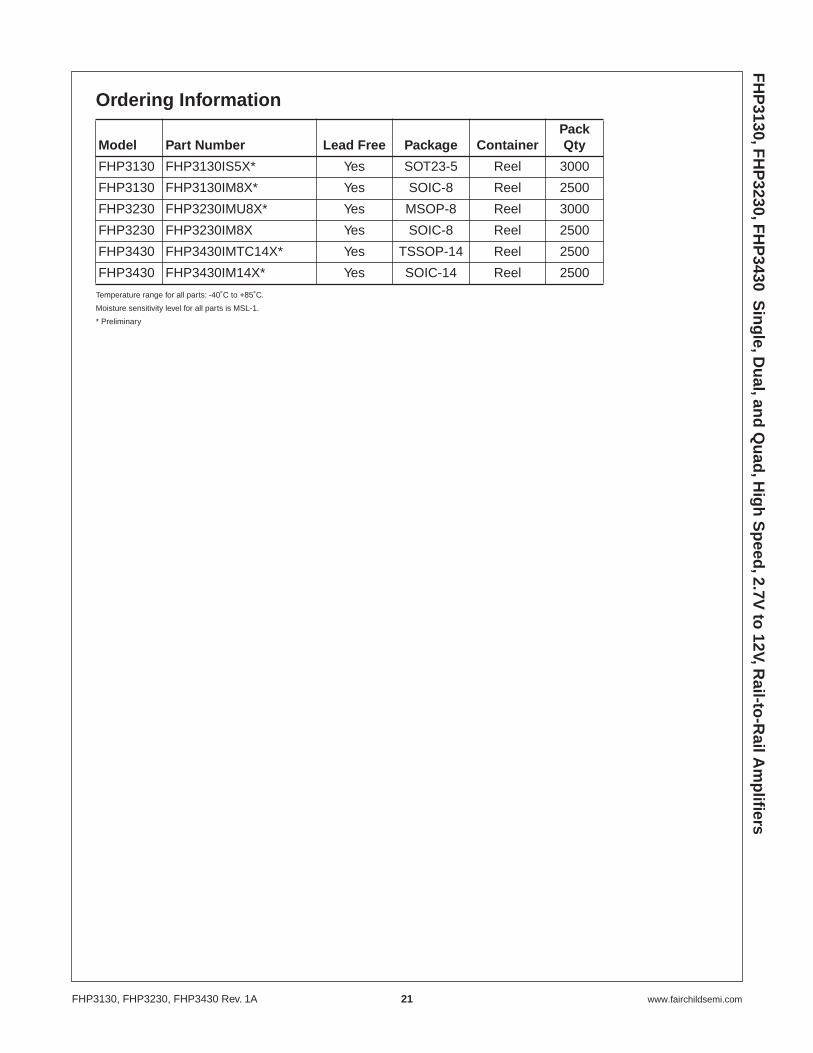
Ordering Information
Temperature range for all parts: -40˚C to +85˚C.
Moisture sensitivity level for all parts is MSL-1.
* Preliminary
Model Part Number Lead Free Package ContainerPack Qty
FHP3130 FHP3130IS5X* Yes SOT23-5 Reel 3000
FHP3130 FHP3130IM8X* Yes SOIC-8 Reel 2500
FHP3230 FHP3230IMU8X* Yes MSOP-8 Reel 3000
FHP3230 FHP3230IM8X Yes SOIC-8 Reel 2500
FHP3430 FHP3430IMTC14X* Yes TSSOP-14 Reel 2500
FHP3430 FHP3430IM14X* Yes SOIC-14 Reel 2500

www.fairchildsemi.com 22 ©2005 Fairchild Semiconductor Corporation
FH
P3130, F
HP
3230, FH
P3430 S
ing
le, Du
al, and
Qu
ad, H
igh
Sp
eed, 2.7V
to 12V, R
ail-to-R
ail Am
plifi
ers
DISCLAIMER
FAIRCHILD SEMICONDUCTOR RESERVES THE RIGHT TO MAKE CHANGES WITHOUT FURTHER NOTICE TO ANYPRODUCTS HEREIN TO IMPROVE RELIABILITY, FUNCTION OR DESIGN. FAIRCHILD DOES NOT ASSUME ANY LIABILITYARISING OUT OF THE APPLICATION OR USE OF ANY PRODUCT OR CIRCUIT DESCRIBED HEREIN; NEITHER DOES ITCONVEY ANY LICENSE UNDER ITS PATENT RIGHTS, NOR THE RIGHTS OF OTHERS.
TRADEMARKS
The following are registered and unregistered trademarks Fairchild Semiconductor owns or is authorized to use and isnot intended to be an exhaustive list of all such trademarks.
LIFE SUPPORT POLICY
FAIRCHILD’S PRODUCTS ARE NOT AUTHORIZED FOR USE AS CRITICAL COMPONENTS IN LIFE SUPPORTDEVICES OR SYSTEMS WITHOUT THE EXPRESS WRITTEN APPROVAL OF FAIRCHILD SEMICONDUCTOR CORPORATION.As used herein:1. Life support devices or systems are devices orsystems which, (a) are intended for surgical implant intothe body, or (b) support or sustain life, or (c) whosefailure to perform when properly used in accordancewith instructions for use provided in the labeling, can bereasonably expected to result in significant injury to theuser.
2. A critical component is any component of a lifesupport device or system whose failure to perform canbe reasonably expected to cause the failure of the lifesupport device or system, or to affect its safety oreffectiveness.
PRODUCT STATUS DEFINITIONS
Definition of Terms
Datasheet Identification Product Status Definition
Advance Information
Preliminary
No Identification Needed
Obsolete
This datasheet contains the design specifications forproduct development. Specifications may change inany manner without notice.
This datasheet contains preliminary data, andsupplementary data will be published at a later date.Fairchild Semiconductor reserves the right to makechanges at any time without notice in order to improvedesign.
This datasheet contains final specifications. FairchildSemiconductor reserves the right to make changes atany time without notice in order to improve design.
This datasheet contains specifications on a productthat has been discontinued by Fairchild semiconductor.The datasheet is printed for reference information only.
Formative orIn Design
First Production
Full Production
Not In Production
ISOPLANAR™ LittleFET™
MICROCOUPLER™MicroFET™MicroPak™MICROWIRE™MSX™MSXPro™OCX™OCXPro™OPTOLOGICOPTOPLANAR™PACMAN™POP™Power247™PowerEdge™
FASTFASTr™
FPS™FRFET™GlobalOptoisolator™GTO™HiSeC™I2C™i-Lo™ImpliedDisconnect™IntelliMAX™
Rev. I16
ACEx™ActiveArray™Bottomless™Build it Now™CoolFET™CROSSVOLT™DOME™EcoSPARK™E2CMOS™EnSigna™FACT™FACT Quiet Series™
PowerSaver™PowerTrenchQFETQS™QT Optoelectronics™Quiet Series™RapidConfigure™RapidConnect™µSerDes™SILENT SWITCHERSMART START™SPM™Stealth™SuperFET™SuperSOT™-3SuperSOT™-6
SuperSOT™-8SyncFET™TinyLogicTINYOPTO™TruTranslation™UHC™UltraFETUniFET™VCX™Wire™
Across the board. Around the world.™The Power FranchiseProgrammable Active Droop™
Top Related