


Languages
Pages
Legal

FFT IP CoreUser Guide
Updated for Intel® Quartus® Prime Design Suite: 17.1
SubscribeSend Feedback
UG-FFT | 2017.11.06Latest document on the web: PDF | HTML
Contents
1. About This IP Core......................................................................................................... 41.1. Intel® DSP IP Core Features....................................................................................41.2. FFT IP Core Features..............................................................................................51.3. General Description...............................................................................................5
1.3.1. Fixed Transform Size FFT........................................................................... 51.3.2. Variable Streaming FFT..............................................................................6
1.4. DSP IP Core Device Family Support..........................................................................61.5. DSP IP Core Verification..........................................................................................71.6. FFT IP Core Release Information.............................................................................71.7. Performance and Resource Utilization...................................................................... 7
2. FFT IP Core Getting Started.......................................................................................... 132.1. Installing and Licensing Intel FPGA IP Cores............................................................ 13
2.1.1. Intel FPGA IP Evaluation Mode................................................................... 132.1.2. FFT IP Core Intel FPGA IP Evaluation Mode Timeout Behavior.........................16
2.2. IP Catalog and Parameter Editor............................................................................ 162.3. Generating IP Cores (Intel Quartus Prime Pro Edition)...............................................17
2.3.1. IP Core Generation Output (Intel Quartus Prime Pro Edition)..........................192.4. Generating IP Cores (Intel Quartus Prime Standard Edition)...................................... 21
2.4.1. IP Core Generation Output (Intel Quartus Prime Standard Edition)..................222.5. Simulating Intel FPGA IP Cores.............................................................................. 23
2.5.1. Simulating the Fixed-Transform FFT IP Core in the MATLAB Software...............242.5.2. Simulating the Variable Streaming FFT IP Core in the MATLAB Software.......... 24
2.6. DSP Builder for Intel FPGAs Design Flow................................................................. 25
3. FFT IP Core Functional Description.............................................................................. 263.1. Fixed Transform FFTs...........................................................................................263.2. Variable Streaming FFTs.......................................................................................26
3.2.1. Fixed-Point Variable Streaming FFTs.......................................................... 273.2.2. Floating-Point Variable Streaming FFTs.......................................................27
3.3. FFT Processor Engines......................................................................................... 273.3.1. Quad-Output FFT Engine..........................................................................283.3.2. Single-Output FFT Engine.........................................................................28
3.4. I/O Data Flow.....................................................................................................293.4.1. Streaming FFT........................................................................................293.4.2. Variable Streaming..................................................................................313.4.3. Buffered Burst........................................................................................ 343.4.4. Burst.....................................................................................................36
3.5. FFT IP Core Parameters....................................................................................... 373.6. FFT IP Core Interfaces and Signals........................................................................ 38
3.6.1. Avalon-ST Interfaces in DSP IP Cores......................................................... 383.6.2. FFT IP Core Avalon-ST Signals................................................................... 39
4. Block Floating Point Scaling......................................................................................... 424.1. Possible Exponent Values..................................................................................... 434.2. Implementing Scaling..........................................................................................44
4.2.1. Example of Scaling..................................................................................444.3. Unity Gain in an IFFT+FFT Pair............................................................................. 46
Contents
FFT IP Core: User Guide Send Feedback
2

5. Document Revision History........................................................................................... 48
A. FFT IP Core User Guide Document Archive....................................................................50
Contents
Send Feedback FFT IP Core: User Guide
3
1. About This IP CoreRelated Information
• FFT IP Core User Guide Document Archive on page 50Provides a list of user guides for previous versions of the FFT IP core.
• Introduction to Intel FPGA IP CoresProvides general information about all Intel FPGA IP cores, includingparameterizing, generating, upgrading, and simulating IP cores.
• Creating Version-Independent IP and Qsys Simulation ScriptsCreate simulation scripts that do not require manual updates for software or IPversion upgrades.
• Project Management Best PracticesGuidelines for efficient management and portability of your project and IP files.
1.1. Intel® DSP IP Core Features
• Avalon® Streaming (Avalon-ST) interfaces
• DSP Builder for Intel® FPGAs ready
• Testbenches to verify the IP core
• IP functional simulation models for use in Intel-supported VHDL and Verilog HDLsimulators
UG-FFT | 2017.11.06
Send Feedback
Intel Corporation. All rights reserved. Agilex, Altera, Arria, Cyclone, Enpirion, Intel, the Intel logo, MAX, Nios,Quartus and Stratix words and logos are trademarks of Intel Corporation or its subsidiaries in the U.S. and/orother countries. Intel warrants performance of its FPGA and semiconductor products to current specifications inaccordance with Intel's standard warranty, but reserves the right to make changes to any products and servicesat any time without notice. Intel assumes no responsibility or liability arising out of the application or use of anyinformation, product, or service described herein except as expressly agreed to in writing by Intel. Intelcustomers are advised to obtain the latest version of device specifications before relying on any publishedinformation and before placing orders for products or services.*Other names and brands may be claimed as the property of others.
ISO9001:2015Registered

1.2. FFT IP Core Features
• Bit-accurate MATLAB models
• Variable streaming FFT:
— Single-precision floating-point or fixed-point representation
— Radix-4, mixed radix-4/2 implementations (for floating-point FFT), andradix-22 single delay feedback implementation (for fixed-point FFT)
— Input and output orders: natural order, or digit-reversed, and DC-centered (-N/2 to N/2)
— Reduced memory requirements
— Support for 8 to 32-bit data and twiddle width (fixed-point FFTs)
• Fixed transform size FFT that implements block floating-point FFTs and maintainsthe maximum dynamic range of data during processing (not for variable streamingFFTs)
— Multiple I/O data flow options: streaming, buffered burst, and burst
— Uses embedded memory
— Maximum system clock frequency more than 300 MHz
— Optimized to use Stratix series DSP blocks and TriMatrix memory
— High throughput quad-output radix 4 FFT engine
— Support for multiple single-output and quad-output engines in parallel
• User control over optimization in DSP blocks or in speed in Stratix V devices, forstreaming, buffered burst, burst, and variable streaming fixed-point FFTs
• Avalon Streaming (Avalon-ST) compliant input and output interfaces
• Parameterization-specific VHDL and Verilog HDL testbench generation
• Transform direction (FFT/IFFT) specifiable on a per-block basis
1.3. General Description
The FFT IP core is a high performance, highly-parameterizable Fast Fourier transform(FFT) processor. The FFT IP core implements a complex FFT or inverse FFT (IFFT) forhigh-performance applications.
The FFT MegaCore function implements:
• Fixed transform size FFT
• Variable streaming FFT
1.3.1. Fixed Transform Size FFT
The fixed transform FFT implements a radix-2/4 decimation-in-frequency (DIF) FFTfixed-transform size algorithm for transform lengths of 2m where 6 ≤ m ≤16. This FFTuses block-floating point representations to achieve the best trade-off betweenmaximum signal-to-noise ratio (SNR) and minimum size requirements.
The fixed transform FFT accepts a two's complement format complex data vector oflength N inputs, where N is the desired transform length in natural order. The functionoutputs the transform-domain complex vector in natural order. The FFT produces an
1. About This IP Core
UG-FFT | 2017.11.06
Send Feedback FFT IP Core: User Guide
5

accumulated block exponent to indicate any data scaling that has occurred during thetransform to maintain precision and maximize the internal signal-to-noise ratio. Youcan specify the transform direction on a per-block basis using an input port.
1.3.2. Variable Streaming FFT
The variable streaming FFT implements two different types of FFT. The variablestreaming FFTs implement either a radix-22 single delay feedback FFT, using a fixed-point representation, or a mixed radix-4/2 FFT, using a single precision floating pointrepresentation. After you select your FFT type, you can configure your FFT variationduring runtime to perform the FFT algorithm for transform lengths of 2m where 3 ≤ m≤18.
The fixed-point representation grows the data widths naturally from input through tooutput thereby maintaining a high SNR at the output. The single precision floating-point representation allows a large dynamic range of values to be represented whilemaintaining a high SNR at the output.
The order of the input data vector of size N can be natural or digit-reversed, or -N/2 toN/2 (DC-centered). The fixed-point representation supports a natural or DC-centeredorder and the floating point representation supports a natural, digit-reversed order.The FFT outputs the transform-domain complex vector in natural or digit-reversedorder. You can specify the transform direction on a per-block basis using an input port.
1.4. DSP IP Core Device Family Support
Intel offers the following device support levels for Intel FPGA IP cores:
• Advance support—the IP core is available for simulation and compilation for thisdevice family. FPGA programming file (.pof) support is not available for QuartusPrime Pro Stratix 10 Edition Beta software and as such IP timing closure cannot beguaranteed. Timing models include initial engineering estimates of delays basedon early post-layout information. The timing models are subject to change assilicon testing improves the correlation between the actual silicon and the timingmodels. You can use this IP core for system architecture and resource utilizationstudies, simulation, pinout, system latency assessments, basic timing assessments(pipeline budgeting), and I/O transfer strategy (data-path width, burst depth, I/Ostandards tradeoffs).
• Preliminary support—Intel verifies the IP core with preliminary timing models forthis device family. The IP core meets all functional requirements, but might still beundergoing timing analysis for the device family. You can use it in productiondesigns with caution.
• Final support—Intel verifies the IP core with final timing models for this devicefamily. The IP core meets all functional and timing requirements for the devicefamily. You can use it in production designs.
Table 1. DSP IP Core Device Family Support
Device Family Support
Arria® II GX Final
Arria II GZ Final
Arria V Final
continued...
1. About This IP Core
UG-FFT | 2017.11.06
FFT IP Core: User Guide Send Feedback
6
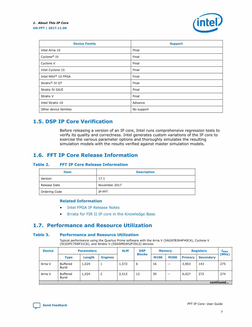
Device Family Support
Intel Arria 10 Final
Cyclone® IV Final
Cyclone V Final
Intel Cyclone 10 Final
Intel MAX® 10 FPGA Final
Stratix® IV GT Final
Stratix IV GX/E Final
Stratix V Final
Intel Stratix 10 Advance
Other device families No support
1.5. DSP IP Core Verification
Before releasing a version of an IP core, Intel runs comprehensive regression tests toverify its quality and correctness. Intel generates custom variations of the IP core toexercise the various parameter options and thoroughly simulates the resultingsimulation models with the results verified against master simulation models.
1.6. FFT IP Core Release Information
Table 2. FFT IP Core Release Information
Item Description
Version 17.1
Release Date November 2017
Ordering Code IP-FFT
Related Information
• Intel FPGA IP Release Notes
• Errata for FIR II IP core in the Knowledge Base
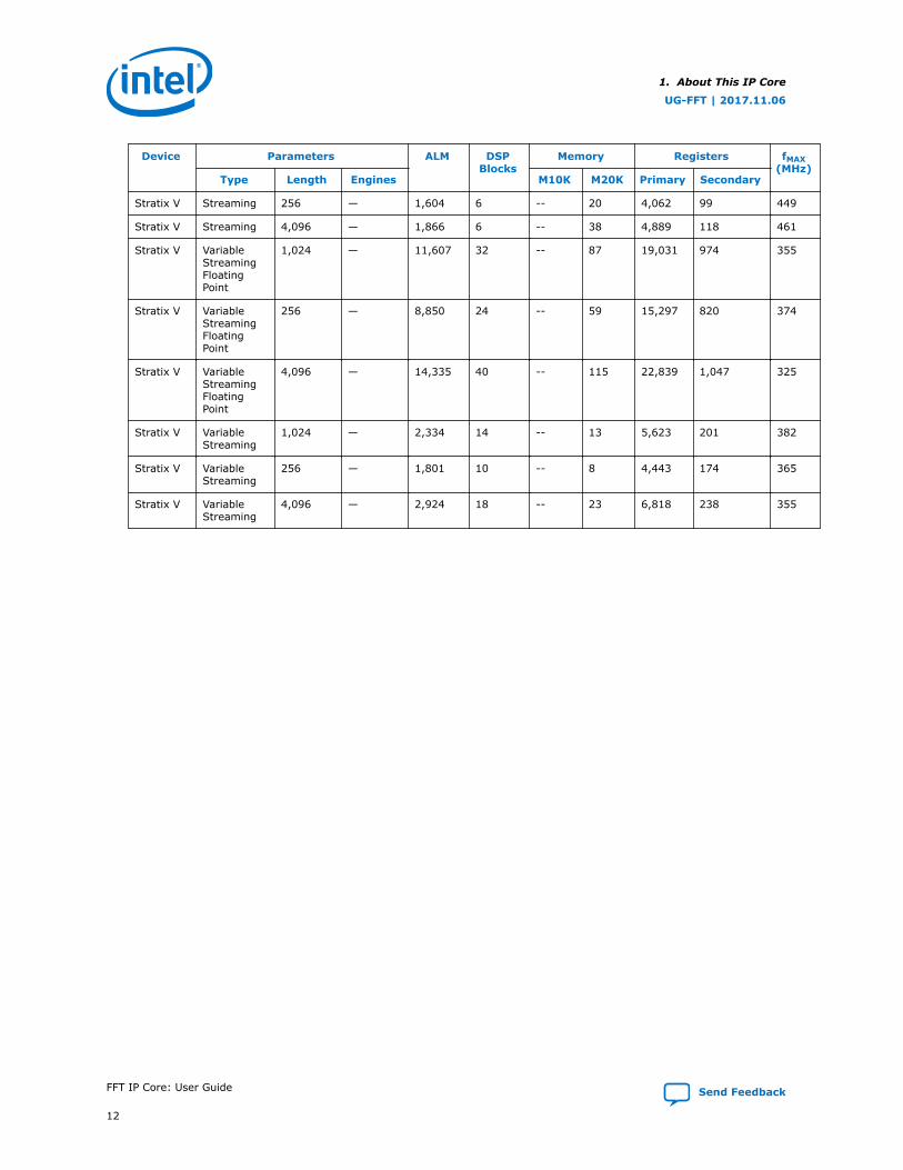
1.7. Performance and Resource Utilization
Table 3. Performance and Resource UtilizationTypical performance using the Quartus Prime software with the Arria V (5AGXFB3H4F40C4), Cyclone V(5CGXFC7D6F31C6), and Stratix V (5SGSMD4H2F35C2) devices
Device Parameters ALM DSPBlocks
Memory Registers fMAX(MHz)
Type Length Engines M10K M20K Primary Secondary
Arria V BufferedBurst
1,024 1 1,572 6 16 -- 3,903 143 275
Arria V BufferedBurst
1,024 2 2,512 12 30 -- 6,027 272 274
continued...
1. About This IP Core
UG-FFT | 2017.11.06
Send Feedback FFT IP Core: User Guide
7
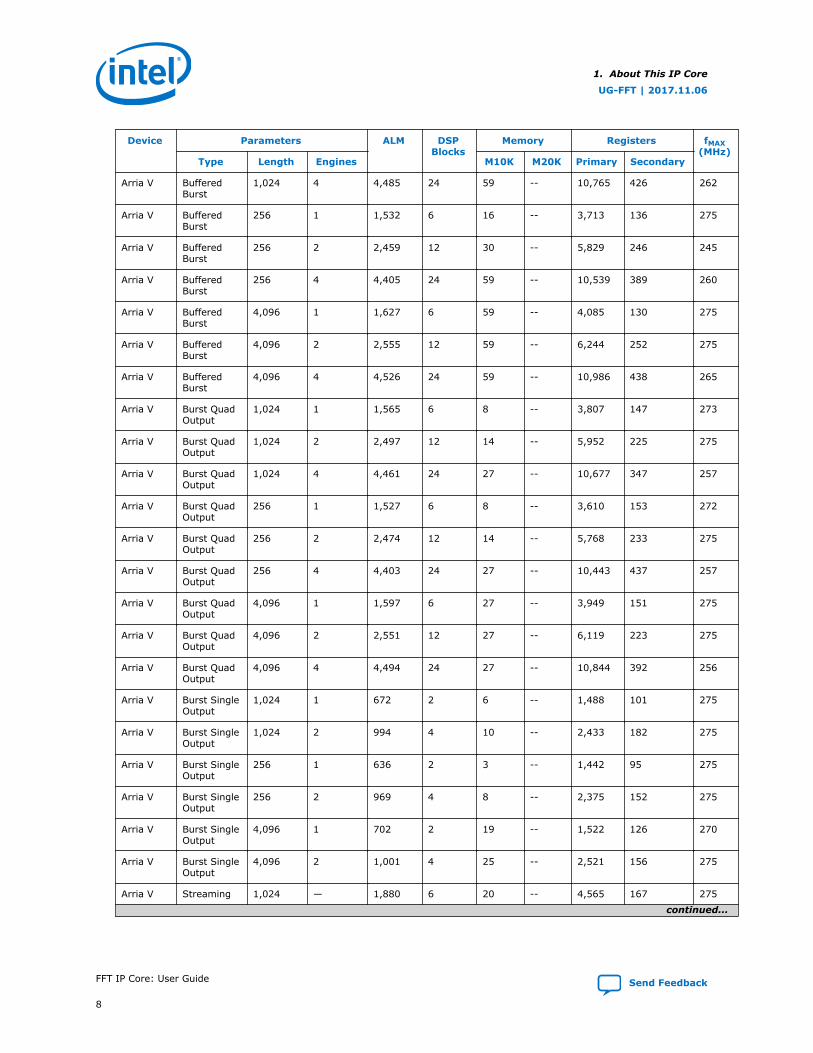
Device Parameters ALM DSPBlocks
Memory Registers fMAX(MHz)
Type Length Engines M10K M20K Primary Secondary
Arria V BufferedBurst
1,024 4 4,485 24 59 -- 10,765 426 262
Arria V BufferedBurst
256 1 1,532 6 16 -- 3,713 136 275
Arria V BufferedBurst
256 2 2,459 12 30 -- 5,829 246 245
Arria V BufferedBurst
256 4 4,405 24 59 -- 10,539 389 260
Arria V BufferedBurst
4,096 1 1,627 6 59 -- 4,085 130 275
Arria V BufferedBurst
4,096 2 2,555 12 59 -- 6,244 252 275
Arria V BufferedBurst
4,096 4 4,526 24 59 -- 10,986 438 265
Arria V Burst QuadOutput
1,024 1 1,565 6 8 -- 3,807 147 273
Arria V Burst QuadOutput
1,024 2 2,497 12 14 -- 5,952 225 275
Arria V Burst QuadOutput
1,024 4 4,461 24 27 -- 10,677 347 257
Arria V Burst QuadOutput
256 1 1,527 6 8 -- 3,610 153 272
Arria V Burst QuadOutput
256 2 2,474 12 14 -- 5,768 233 275
Arria V Burst QuadOutput
256 4 4,403 24 27 -- 10,443 437 257
Arria V Burst QuadOutput
4,096 1 1,597 6 27 -- 3,949 151 275
Arria V Burst QuadOutput
4,096 2 2,551 12 27 -- 6,119 223 275
Arria V Burst QuadOutput
4,096 4 4,494 24 27 -- 10,844 392 256
Arria V Burst SingleOutput
1,024 1 672 2 6 -- 1,488 101 275
Arria V Burst SingleOutput
1,024 2 994 4 10 -- 2,433 182 275
Arria V Burst SingleOutput
256 1 636 2 3 -- 1,442 95 275
Arria V Burst SingleOutput
256 2 969 4 8 -- 2,375 152 275
Arria V Burst SingleOutput
4,096 1 702 2 19 -- 1,522 126 270
Arria V Burst SingleOutput
4,096 2 1,001 4 25 -- 2,521 156 275
Arria V Streaming 1,024 — 1,880 6 20 -- 4,565 167 275
continued...
1. About This IP Core
UG-FFT | 2017.11.06
FFT IP Core: User Guide Send Feedback
8
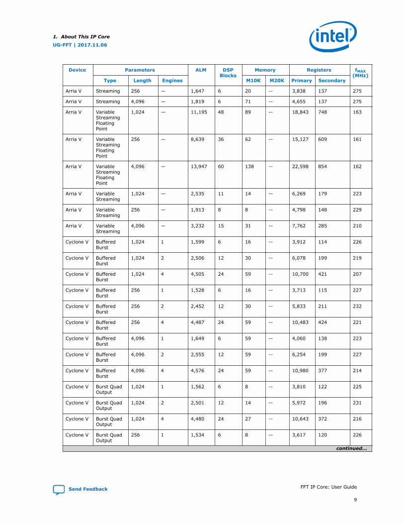
Device Parameters ALM DSPBlocks
Memory Registers fMAX(MHz)
Type Length Engines M10K M20K Primary Secondary
Arria V Streaming 256 — 1,647 6 20 -- 3,838 137 275
Arria V Streaming 4,096 — 1,819 6 71 -- 4,655 137 275
Arria V VariableStreamingFloatingPoint
1,024 — 11,195 48 89 -- 18,843 748 163
Arria V VariableStreamingFloatingPoint
256 — 8,639 36 62 -- 15,127 609 161
Arria V VariableStreamingFloatingPoint
4,096 — 13,947 60 138 -- 22,598 854 162
Arria V VariableStreaming
1,024 — 2,535 11 14 -- 6,269 179 223
Arria V VariableStreaming
256 — 1,913 8 8 -- 4,798 148 229
Arria V VariableStreaming
4,096 — 3,232 15 31 -- 7,762 285 210
Cyclone V BufferedBurst
1,024 1 1,599 6 16 -- 3,912 114 226
Cyclone V BufferedBurst
1,024 2 2,506 12 30 -- 6,078 199 219
Cyclone V BufferedBurst
1,024 4 4,505 24 59 -- 10,700 421 207
Cyclone V BufferedBurst
256 1 1,528 6 16 -- 3,713 115 227
Cyclone V BufferedBurst
256 2 2,452 12 30 -- 5,833 211 232
Cyclone V BufferedBurst
256 4 4,487 24 59 -- 10,483 424 221
Cyclone V BufferedBurst
4,096 1 1,649 6 59 -- 4,060 138 223
Cyclone V BufferedBurst
4,096 2 2,555 12 59 -- 6,254 199 227
Cyclone V BufferedBurst
4,096 4 4,576 24 59 -- 10,980 377 214
Cyclone V Burst QuadOutput
1,024 1 1,562 6 8 -- 3,810 122 225
Cyclone V Burst QuadOutput
1,024 2 2,501 12 14 -- 5,972 196 231
Cyclone V Burst QuadOutput
1,024 4 4,480 24 27 -- 10,643 372 216
Cyclone V Burst QuadOutput
256 1 1,534 6 8 -- 3,617 120 226
continued...
1. About This IP Core
UG-FFT | 2017.11.06
Send Feedback FFT IP Core: User Guide
9
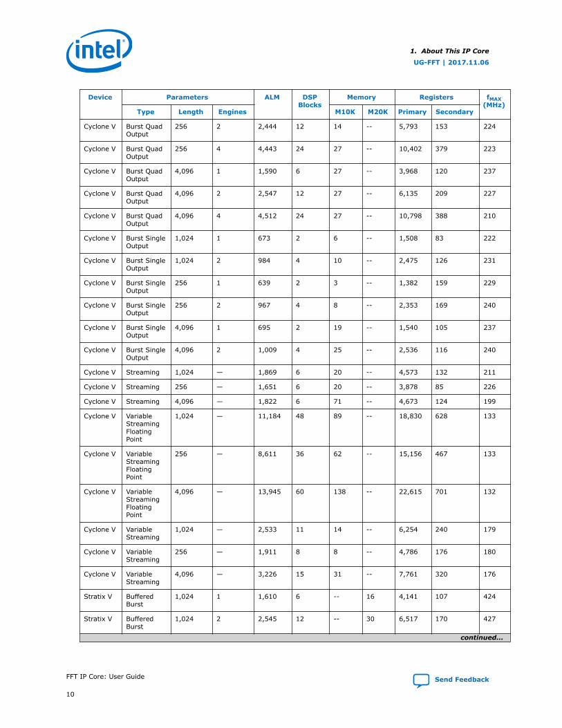
Device Parameters ALM DSPBlocks
Memory Registers fMAX(MHz)
Type Length Engines M10K M20K Primary Secondary
Cyclone V Burst QuadOutput
256 2 2,444 12 14 -- 5,793 153 224
Cyclone V Burst QuadOutput
256 4 4,443 24 27 -- 10,402 379 223
Cyclone V Burst QuadOutput
4,096 1 1,590 6 27 -- 3,968 120 237
Cyclone V Burst QuadOutput
4,096 2 2,547 12 27 -- 6,135 209 227
Cyclone V Burst QuadOutput
4,096 4 4,512 24 27 -- 10,798 388 210
Cyclone V Burst SingleOutput
1,024 1 673 2 6 -- 1,508 83 222
Cyclone V Burst SingleOutput
1,024 2 984 4 10 -- 2,475 126 231
Cyclone V Burst SingleOutput
256 1 639 2 3 -- 1,382 159 229
Cyclone V Burst SingleOutput
256 2 967 4 8 -- 2,353 169 240
Cyclone V Burst SingleOutput
4,096 1 695 2 19 -- 1,540 105 237
Cyclone V Burst SingleOutput
4,096 2 1,009 4 25 -- 2,536 116 240
Cyclone V Streaming 1,024 — 1,869 6 20 -- 4,573 132 211
Cyclone V Streaming 256 — 1,651 6 20 -- 3,878 85 226
Cyclone V Streaming 4,096 — 1,822 6 71 -- 4,673 124 199
Cyclone V VariableStreamingFloatingPoint
1,024 — 11,184 48 89 -- 18,830 628 133
Cyclone V VariableStreamingFloatingPoint
256 — 8,611 36 62 -- 15,156 467 133
Cyclone V VariableStreamingFloatingPoint
4,096 — 13,945 60 138 -- 22,615 701 132
Cyclone V VariableStreaming
1,024 — 2,533 11 14 -- 6,254 240 179
Cyclone V VariableStreaming
256 — 1,911 8 8 -- 4,786 176 180
Cyclone V VariableStreaming
4,096 — 3,226 15 31 -- 7,761 320 176
Stratix V BufferedBurst
1,024 1 1,610 6 -- 16 4,141 107 424
Stratix V BufferedBurst
1,024 2 2,545 12 -- 30 6,517 170 427
continued...
1. About This IP Core
UG-FFT | 2017.11.06
FFT IP Core: User Guide Send Feedback
10
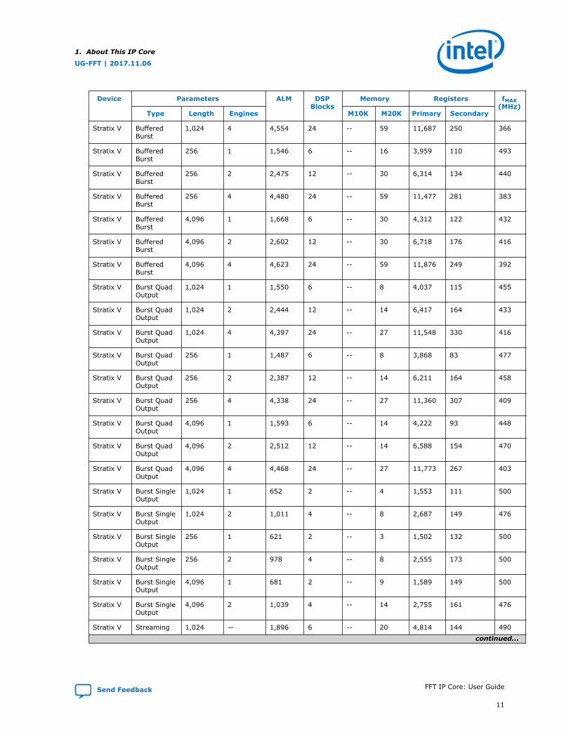
Device Parameters ALM DSPBlocks
Memory Registers fMAX(MHz)
Type Length Engines M10K M20K Primary Secondary
Stratix V BufferedBurst
1,024 4 4,554 24 -- 59 11,687 250 366
Stratix V BufferedBurst
256 1 1,546 6 -- 16 3,959 110 493
Stratix V BufferedBurst
256 2 2,475 12 -- 30 6,314 134 440
Stratix V BufferedBurst
256 4 4,480 24 -- 59 11,477 281 383
Stratix V BufferedBurst
4,096 1 1,668 6 -- 30 4,312 122 432
Stratix V BufferedBurst
4,096 2 2,602 12 -- 30 6,718 176 416
Stratix V BufferedBurst
4,096 4 4,623 24 -- 59 11,876 249 392
Stratix V Burst QuadOutput
1,024 1 1,550 6 -- 8 4,037 115 455
Stratix V Burst QuadOutput
1,024 2 2,444 12 -- 14 6,417 164 433
Stratix V Burst QuadOutput
1,024 4 4,397 24 -- 27 11,548 330 416
Stratix V Burst QuadOutput
256 1 1,487 6 -- 8 3,868 83 477
Stratix V Burst QuadOutput
256 2 2,387 12 -- 14 6,211 164 458
Stratix V Burst QuadOutput
256 4 4,338 24 -- 27 11,360 307 409
Stratix V Burst QuadOutput
4,096 1 1,593 6 -- 14 4,222 93 448
Stratix V Burst QuadOutput
4,096 2 2,512 12 -- 14 6,588 154 470
Stratix V Burst QuadOutput
4,096 4 4,468 24 -- 27 11,773 267 403
Stratix V Burst SingleOutput
1,024 1 652 2 -- 4 1,553 111 500
Stratix V Burst SingleOutput
1,024 2 1,011 4 -- 8 2,687 149 476
Stratix V Burst SingleOutput
256 1 621 2 -- 3 1,502 132 500
Stratix V Burst SingleOutput
256 2 978 4 -- 8 2,555 173 500
Stratix V Burst SingleOutput
4,096 1 681 2 -- 9 1,589 149 500
Stratix V Burst SingleOutput
4,096 2 1,039 4 -- 14 2,755 161 476
Stratix V Streaming 1,024 — 1,896 6 -- 20 4,814 144 490
continued...
1. About This IP Core
UG-FFT | 2017.11.06
Send Feedback FFT IP Core: User Guide
11
Device Parameters ALM DSPBlocks
Memory Registers fMAX(MHz)
Type Length Engines M10K M20K Primary Secondary
Stratix V Streaming 256 — 1,604 6 -- 20 4,062 99 449
Stratix V Streaming 4,096 — 1,866 6 -- 38 4,889 118 461
Stratix V VariableStreamingFloatingPoint
1,024 — 11,607 32 -- 87 19,031 974 355
Stratix V VariableStreamingFloatingPoint
256 — 8,850 24 -- 59 15,297 820 374
Stratix V VariableStreamingFloatingPoint
4,096 — 14,335 40 -- 115 22,839 1,047 325
Stratix V VariableStreaming
1,024 — 2,334 14 -- 13 5,623 201 382
Stratix V VariableStreaming
256 — 1,801 10 -- 8 4,443 174 365
Stratix V VariableStreaming
4,096 — 2,924 18 -- 23 6,818 238 355
1. About This IP Core
UG-FFT | 2017.11.06
FFT IP Core: User Guide Send Feedback
12
2. FFT IP Core Getting Started
2.1. Installing and Licensing Intel FPGA IP Cores
The Intel Quartus® Prime software installation includes the Intel FPGA IP library. Thislibrary provides many useful IP cores for your production use without the need for anadditional license. Some Intel FPGA IP cores require purchase of a separate license forproduction use. The Intel FPGA IP Evaluation Mode allows you to evaluate theselicensed Intel FPGA IP cores in simulation and hardware, before deciding to purchase afull production IP core license. You only need to purchase a full production license forlicensed Intel IP cores after you complete hardware testing and are ready to use theIP in production.
The Intel Quartus Prime software installs IP cores in the following locations by default:
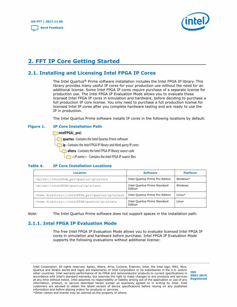
Figure 1. IP Core Installation Path
intelFPGA(_pro)
quartus - Contains the Intel Quartus Prime softwareip - Contains the Intel FPGA IP library and third-party IP cores
altera - Contains the Intel FPGA IP library source code<IP name> - Contains the Intel FPGA IP source files
Table 4. IP Core Installation Locations
Location Software Platform
<drive>:\intelFPGA_pro\quartus\ip\altera Intel Quartus Prime Pro Edition Windows*
<drive>:\intelFPGA\quartus\ip\altera Intel Quartus Prime StandardEdition
Windows
<home directory>:/intelFPGA_pro/quartus/ip/altera Intel Quartus Prime Pro Edition Linux*
<home directory>:/intelFPGA/quartus/ip/altera Intel Quartus Prime StandardEdition
Linux
Note: The Intel Quartus Prime software does not support spaces in the installation path.
2.1.1. Intel FPGA IP Evaluation Mode
The free Intel FPGA IP Evaluation Mode allows you to evaluate licensed Intel FPGA IPcores in simulation and hardware before purchase. Intel FPGA IP Evaluation Modesupports the following evaluations without additional license:
UG-FFT | 2017.11.06
Send Feedback
Intel Corporation. All rights reserved. Agilex, Altera, Arria, Cyclone, Enpirion, Intel, the Intel logo, MAX, Nios,Quartus and Stratix words and logos are trademarks of Intel Corporation or its subsidiaries in the U.S. and/orother countries. Intel warrants performance of its FPGA and semiconductor products to current specifications inaccordance with Intel's standard warranty, but reserves the right to make changes to any products and servicesat any time without notice. Intel assumes no responsibility or liability arising out of the application or use of anyinformation, product, or service described herein except as expressly agreed to in writing by Intel. Intelcustomers are advised to obtain the latest version of device specifications before relying on any publishedinformation and before placing orders for products or services.*Other names and brands may be claimed as the property of others.
ISO9001:2015Registered

• Simulate the behavior of a licensed Intel FPGA IP core in your system.
• Verify the functionality, size, and speed of the IP core quickly and easily.
• Generate time-limited device programming files for designs that include IP cores.
• Program a device with your IP core and verify your design in hardware.
Intel FPGA IP Evaluation Mode supports the following operation modes:
• Tethered—Allows running the design containing the licensed Intel FPGA IPindefinitely with a connection between your board and the host computer.Tethered mode requires a serial joint test action group (JTAG) cable connectedbetween the JTAG port on your board and the host computer, which is running theIntel Quartus Prime Programmer for the duration of the hardware evaluationperiod. The Programmer only requires a minimum installation of the Intel QuartusPrime software, and requires no Intel Quartus Prime license. The host computercontrols the evaluation time by sending a periodic signal to the device via theJTAG port. If all licensed IP cores in the design support tethered mode, theevaluation time runs until any IP core evaluation expires. If all of the IP coressupport unlimited evaluation time, the device does not time-out.
• Untethered—Allows running the design containing the licensed IP for a limitedtime. The IP core reverts to untethered mode if the device disconnects from thehost computer running the Intel Quartus Prime software. The IP core also revertsto untethered mode if any other licensed IP core in the design does not supporttethered mode.
When the evaluation time expires for any licensed Intel FPGA IP in the design, thedesign stops functioning. All IP cores that use the Intel FPGA IP Evaluation Mode timeout simultaneously when any IP core in the design times out. When the evaluationtime expires, you must reprogram the FPGA device before continuing hardwareverification. To extend use of the IP core for production, purchase a full productionlicense for the IP core.
You must purchase the license and generate a full production license key before youcan generate an unrestricted device programming file. During Intel FPGA IP EvaluationMode, the Compiler only generates a time-limited device programming file (<projectname>_time_limited.sof) that expires at the time limit.
2. FFT IP Core Getting Started
UG-FFT | 2017.11.06
FFT IP Core: User Guide Send Feedback
14

Figure 2. Intel FPGA IP Evaluation Mode Flow
Install the Intel Quartus Prime Software with Intel FPGA IP Library
Parameterize and Instantiate aLicensed Intel FPGA IP Core
Purchase a Full Production IP License
Verify the IP in a Supported Simulator
Compile the Design in theIntel Quartus Prime Software
Generate a Time-Limited DeviceProgramming File
Program the Intel FPGA Deviceand Verify Operation on the Board
No
Yes
IP Ready forProduction Use?
Include Licensed IP in Commercial Products
Note: Refer to each IP core's user guide for parameterization steps and implementationdetails.
Intel licenses IP cores on a per-seat, perpetual basis. The license fee includes first-year maintenance and support. You must renew the maintenance contract to receiveupdates, bug fixes, and technical support beyond the first year. You must purchase afull production license for Intel FPGA IP cores that require a production license, beforegenerating programming files that you may use for an unlimited time. During IntelFPGA IP Evaluation Mode, the Compiler only generates a time-limited deviceprogramming file (<project name>_time_limited.sof) that expires at the timelimit. To obtain your production license keys, visit the Self-Service Licensing Center.
The Intel FPGA Software License Agreements govern the installation and use oflicensed IP cores, the Intel Quartus Prime design software, and all unlicensed IP cores.
2. FFT IP Core Getting Started
UG-FFT | 2017.11.06
Send Feedback FFT IP Core: User Guide
15
Related Information
• Intel Quartus Prime Licensing Site
• Introduction to Intel FPGA Software Installation and Licensing
2.1.2. FFT IP Core Intel FPGA IP Evaluation Mode Timeout Behavior
All IP cores in a device time out simultaneously when the most restrictive evaluationtime is reached. If a design has more than one IP core, the time-out behavior of theother IP cores may mask the time-out behavior of a specific IP core .
For IP cores, the untethered time-out is 1 hour; the tethered time-out value isindefinite. Your design stops working after the hardware evaluation time expires. TheQuartus Prime software uses Intel FPGA IP Evaluation Mode Files (.ocp) in yourproject directory to identify your use of the Intel FPGA IP Evaluation Mode evaluationprogram. After you activate the feature, do not delete these files..
When the evaluation time expires, the source_real, source_imag, andsource_exp signals go low.
Related Information
AN 320: OpenCore Plus Evaluation of Megafunctions
2.2. IP Catalog and Parameter Editor
The IP Catalog displays the IP cores available for your project, including Intel FPGA IPand other IP that you add to the IP Catalog search path.. Use the following features ofthe IP Catalog to locate and customize an IP core:
• Filter IP Catalog to Show IP for active device family or Show IP for alldevice families. If you have no project open, select the Device Family in IPCatalog.
• Type in the Search field to locate any full or partial IP core name in IP Catalog.
• Right-click an IP core name in IP Catalog to display details about supporteddevices, to open the IP core's installation folder, and for links to IP documentation.
• Click Search for Partner IP to access partner IP information on the web.
The parameter editor prompts you to specify an IP variation name, optional ports, andoutput file generation options. The parameter editor generates a top-level IntelQuartus Prime IP file (.ip) for an IP variation in Intel Quartus Prime Pro Editionprojects.
The parameter editor generates a top-level Quartus IP file (.qip) for an IP variationin Intel Quartus Prime Standard Edition projects. These files represent the IP variationin the project, and store parameterization information.
2. FFT IP Core Getting Started
UG-FFT | 2017.11.06
FFT IP Core: User Guide Send Feedback
16
Figure 3. IP Parameter Editor (Intel Quartus Prime Standard Edition)
2.3. Generating IP Cores (Intel Quartus Prime Pro Edition)
Quickly configure Intel FPGA IP cores in the Intel Quartus Prime parameter editor.Double-click any component in the IP Catalog to launch the parameter editor. Theparameter editor allows you to define a custom variation of the IP core. The parametereditor generates the IP variation synthesis and optional simulation files, and addsthe .ip file representing the variation to your project automatically.
Follow these steps to locate, instantiate, and customize an IP core in the parametereditor:
1. Create or open an Intel Quartus Prime project (.qpf) to contain the instantiatedIP variation.
2. In the IP Catalog (Tools ➤ IP Catalog), locate and double-click the name of theIP core to customize. To locate a specific component, type some or all of thecomponent’s name in the IP Catalog search box. The New IP Variation windowappears.
3. Specify a top-level name for your custom IP variation. Do not include spaces in IPvariation names or paths. The parameter editor saves the IP variation settings in afile named <your_ip>.ip. Click OK. The parameter editor appears.
2. FFT IP Core Getting Started
UG-FFT | 2017.11.06
Send Feedback FFT IP Core: User Guide
17

Figure 4. IP Parameter Editor (Intel Quartus Prime Pro Edition)
4. Set the parameter values in the parameter editor and view the block diagram forthe component. The Parameterization Messages tab at the bottom displays anyerrors in IP parameters:
• Optionally, select preset parameter values if provided for your IP core. Presetsspecify initial parameter values for specific applications.
• Specify parameters defining the IP core functionality, port configurations, anddevice-specific features.
• Specify options for processing the IP core files in other EDA tools.
Note: Refer to your IP core user guide for information about specific IP coreparameters.
5. Click Generate HDL. The Generation dialog box appears.
6. Specify output file generation options, and then click Generate. The synthesis andsimulation files generate according to your specifications.
7. To generate a simulation testbench, click Generate ➤ Generate TestbenchSystem. Specify testbench generation options, and then click Generate.
8. To generate an HDL instantiation template that you can copy and paste into yourtext editor, click Generate ➤ Show Instantiation Template.
9. Click Finish. Click Yes if prompted to add files representing the IP variation toyour project.
10. After generating and instantiating your IP variation, make appropriate pinassignments to connect ports.
2. FFT IP Core Getting Started
UG-FFT | 2017.11.06
FFT IP Core: User Guide Send Feedback
18
Note: Some IP cores generate different HDL implementations according to the IPcore parameters. The underlying RTL of these IP cores contains a uniquehash code that prevents module name collisions between different variationsof the IP core. This unique code remains consistent, given the same IPsettings and software version during IP generation. This unique code canchange if you edit the IP core's parameters or upgrade the IP core version.To avoid dependency on these unique codes in your simulation environment,refer to Generating a Combined Simulator Setup Script.
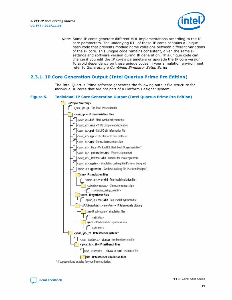
2.3.1. IP Core Generation Output (Intel Quartus Prime Pro Edition)
The Intel Quartus Prime software generates the following output file structure forindividual IP cores that are not part of a Platform Designer system.
Figure 5. Individual IP Core Generation Output (Intel Quartus Prime Pro Edition)
<Project Directory>
<your_ip>_inst.v or .vhd - Lists file for IP core synthesis
<your_ip>.qip - Lists files for IP core synthesis
synth - IP synthesis files
<IP Submodule>_<version> - IP Submodule Library
sim
<your_ip>.v or .vhd - Top-level IP synthesis file
sim - IP simulation files
<simulator vendor> - Simulator setup scripts<simulator_setup_scripts>
<your_ip> - IP core variation files
<your_ip>.ip - Top-level IP variation file
<your_ip>_generation.rpt - IP generation report
<your_ip>.bsf - Block symbol schematic file
<your_ip>.ppf - XML I/O pin information file
<your_ip>.spd - Simulation startup scripts
*
<your_ip>.cmp - VHDL component declaration
<your_ip>.v or vhd - Top-level simulation file
synth
- IP submodule 1 simulation files
- IP submodule 1 synthesis files
<your_ip>_bb.v - Verilog HDL black box EDA synthesis file
<HDL files>
<HDL files>
<your_ip>_tb - IP testbench system *
<your_testbench>_tb.qsys - testbench system file<your_ip>_tb - IP testbench files
your_testbench> _tb.csv or .spd - testbench file
sim - IP testbench simulation files * If supported and enabled for your IP core variation.
<your_ip>.qgsimc - Simulation caching file (Platform Designer)
<your_ip>.qgsynthc - Synthesis caching file (Platform Designer)
2. FFT IP Core Getting Started
UG-FFT | 2017.11.06
Send Feedback FFT IP Core: User Guide
19

Table 5. Output Files of Intel FPGA IP Generation
File Name Description
<your_ip>.ip Top-level IP variation file that contains the parameterization of an IP core inyour project. If the IP variation is part of a Platform Designer system, theparameter editor also generates a .qsys file.
<your_ip>.cmp The VHDL Component Declaration (.cmp) file is a text file that contains localgeneric and port definitions that you use in VHDL design files.
<your_ip>_generation.rpt IP or Platform Designer generation log file. Displays a summary of themessages during IP generation.
<your_ip>.qgsimc (Platform Designersystems only)
Simulation caching file that compares the .qsys and .ip files with the currentparameterization of the Platform Designer system and IP core. This comparisondetermines if Platform Designer can skip regeneration of the HDL.
<your_ip>.qgsynth (PlatformDesigner systems only)
Synthesis caching file that compares the .qsys and .ip files with the currentparameterization of the Platform Designer system and IP core. This comparisondetermines if Platform Designer can skip regeneration of the HDL.
<your_ip>.qip Contains all information to integrate and compile the IP component.
<your_ip>.csv Contains information about the upgrade status of the IP component.
<your_ip>.bsf A symbol representation of the IP variation for use in Block Diagram Files(.bdf).
<your_ip>.spd Input file that ip-make-simscript requires to generate simulation scripts.The .spd file contains a list of files you generate for simulation, along withinformation about memories that you initialize.
<your_ip>.ppf The Pin Planner File (.ppf) stores the port and node assignments for IPcomponents you create for use with the Pin Planner.
<your_ip>_bb.v Use the Verilog blackbox (_bb.v) file as an empty module declaration for useas a blackbox.
<your_ip>_inst.v or _inst.vhd HDL example instantiation template. Copy and paste the contents of this fileinto your HDL file to instantiate the IP variation.
<your_ip>.regmap If the IP contains register information, the Intel Quartus Prime softwaregenerates the .regmap file. The .regmap file describes the register mapinformation of master and slave interfaces. This file complementsthe .sopcinfo file by providing more detailed register information about thesystem. This file enables register display views and user customizable statisticsin System Console.
<your_ip>.svd Allows HPS System Debug tools to view the register maps of peripherals thatconnect to HPS within a Platform Designer system.During synthesis, the Intel Quartus Prime software stores the .svd files forslave interface visible to the System Console masters in the .sof file in thedebug session. System Console reads this section, which Platform Designerqueries for register map information. For system slaves, Platform Designeraccesses the registers by name.
<your_ip>.v
<your_ip>.vhd
HDL files that instantiate each submodule or child IP core for synthesis orsimulation.
mentor/ Contains a msim_setup.tcl script to set up and run a simulation.
aldec/ Contains a script rivierapro_setup.tcl to setup and run a simulation.
/synopsys/vcs
/synopsys/vcsmx
Contains a shell script vcs_setup.sh to set up and run a simulation.Contains a shell script vcsmx_setup.sh and synopsys_sim.setup file toset up and run a simulation.
continued...
2. FFT IP Core Getting Started
UG-FFT | 2017.11.06
FFT IP Core: User Guide Send Feedback
20

File Name Description
/cadence Contains a shell script ncsim_setup.sh and other setup files to set up andrun an simulation.
/xcelium Contains an Parallel simulator shell script xcelium_setup.sh and other setupfiles to set up and run a simulation.
/submodules Contains HDL files for the IP core submodule.
<IP submodule>/ Platform Designer generates /synth and /sim sub-directories for each IPsubmodule directory that Platform Designer generates.
2.4. Generating IP Cores (Intel Quartus Prime Standard Edition)
This topic describes parameterizing and generating an IP variation using a legacyparameter editor in the Intel Quartus Prime Standard Edition software.
Figure 6. Legacy Parameter Editors
Note: The legacy parameter editor generates a different output file structure than the IntelQuartus Prime Pro Edition software.
1. In the IP Catalog (Tools ➤ IP Catalog), locate and double-click the name of theIP core to customize. The parameter editor appears.
2. Specify a top-level name and output HDL file type for your IP variation. This nameidentifies the IP core variation files in your project. Click OK. Do not includespaces in IP variation names or paths.
3. Specify the parameters and options for your IP variation in the parameter editor.Refer to your IP core user guide for information about specific IP core parameters.
4. Click Finish or Generate (depending on the parameter editor version). Theparameter editor generates the files for your IP variation according to yourspecifications. Click Exit if prompted when generation is complete. The parametereditor adds the top-level .qip file to the current project automatically.
2. FFT IP Core Getting Started
UG-FFT | 2017.11.06
Send Feedback FFT IP Core: User Guide
21

Note: For devices released prior to Intel Arria 10 devices, the generated .qipand .sip files must be added to your project to represent IP and PlatformDesigner systems. To manually add an IP variation generated with legacyparameter editor to a project, click Project ➤ Add/Remove Files inProject and add the IP variation .qip file.
2.4.1. IP Core Generation Output (Intel Quartus Prime Standard Edition)
The Intel Quartus Prime Standard Edition software generates one of the followingoutput file structures for individual IP cores that use one of the legacy parametereditors.
2. FFT IP Core Getting Started
UG-FFT | 2017.11.06
FFT IP Core: User Guide Send Feedback
22

Figure 7. IP Core Generated Files (Legacy Parameter Editors)
Generated IP File Output B <Project Directory>
<your_ip>.html - IP core generation report
<your_ip>_testbench.v or .vhd - Testbench file1
<your_ip>.bsf - Block symbol schematic file
<your_ip>_syn.v or .vhd - Timing & resource estimation netlist1
<your_ip>_bb - Verilog HDL black box EDA synthesis file
<your_ip>.vo or .vho - IP functional simulation model 2
<your_ip>.qip - Intel Quartus Prime IP integration file
<your_ip>.v or .vhd - Top-level HDL IP variation definition
<your_ip>_block_period_stim.txt - Testbench simulation data 1
<your_ip>-library - Contains IP subcomponent synthesis libraries
Generated IP File Output A <Project Directory>
<your_ip>.v or .vhd - Top-level IP synthesis file
<your_ip>_inst.v or .vhd - Sample instantiation template
<your_ip>.bsf - Block symbol schematic file
<your_ip>.vo or .vho - IP functional simulation model 2<your_ip>_syn.v or .vhd - Timing & resource estimation netlist1
<your_ip>_bb.v - Verilog HDL black box EDA synthesis file
<your_ip>.qip - Intel Quartus Prime IP integration file
greybox_tmp 3
<your_ip>.cmp - VHDL component declaration file
Generated IP File Output C <Project Directory>
<your_ip>_sim 1
<IP> _instance.vo - IPFS model 2
<simulator_vendor><simulator setup scripts>
<your_ip>.qip - Intel Quartus Prime IP integration file
<your_ip>.sip - Lists files for simulation
<your_ip>_testbench or _example - Testbench or example1
<your_ip>.v, .sv. or .vhd - Top-level IP synthesis file
<IP_name>_instance
<your_ip>_syn.v or .vhd - Timing & resource estimation netlist1<your_ip>.cmp - VHDL component declaration file
<your_ip>.bsf - Block symbol schematic file
<your_ip> - IP core synthesis files
<your_ip>.sv, .v, or .vhd - HDL synthesis files
<your_ip>.sdc - Timing constraints file
<your_ip>.ppf - XML I/O pin information file
<your_ip>.spd - Combines individual simulation scripts 1
<your_ip>_sim.f - Refers to simulation models and scripts 1
Notes:1. If supported and enabled for your IP variation2. If functional simulation models are generated3. Ignore this directory
Generated IP File Output D <Project Directory>
<your_ip>_bb.v - Verilog HDL black box EDA synthesis file
<your_ip>_inst.v or .vhd - Sample instantiation template
synthesis - IP synthesis files
<your_ip>.qip - Lists files for synthesis
testbench - Simulation testbench files 1
<testbench_hdl_files>
<simulator_vendor> - Testbench for supported simulators
<simulation_testbench_files>
<your_ip>.v or .vhd - Top-level IP variation synthesis file
simulation - IP simulation files<your_ip>.sip - NativeLink simulation integration file
<simulator vendor> - Simulator setup scripts<simulator_setup_scripts>
<your_ip> - IP core variation files
<your_ip>.qip or .qsys - System or IP integration file
<your_ip>_generation.rpt - IP generation report
<your_ip>.bsf - Block symbol schematic file
<your_ip>.ppf - XML I/O pin information file
<your_ip>.spd - Combines individual simulation startup scripts 1
<your_ip>.html - Contains memory map
<your_ip>.sopcinfo - Software tool-chain integration file
<your_ip>_syn.v or .vhd - Timing & resource estimation netlist 1
<your_ip>.debuginfo - Lists files for synthesis
<your_ip>.v, .vhd, .vo, .vho - HDL or IPFS models2
<your_ip>_tb - Testbench for supported simulators<your_ip>_tb.v or .vhd - Top-level HDL testbench file
2.5. Simulating Intel FPGA IP Cores
The Intel Quartus Prime software supports IP core RTL simulation in specific EDAsimulators. IP generation creates simulation files, including the functional simulationmodel, any testbench (or example design), and vendor-specific simulator setup scriptsfor each IP core. Use the functional simulation model and any testbench or exampledesign for simulation. IP generation output may also include scripts to compile and runany testbench. The scripts list all models or libraries you require to simulate your IPcore.
2. FFT IP Core Getting Started
UG-FFT | 2017.11.06
Send Feedback FFT IP Core: User Guide
23

The Intel Quartus Prime software provides integration with many simulators andsupports multiple simulation flows, including your own scripted and custom simulationflows. Whichever flow you choose, IP core simulation involves the following steps:
1. Generate simulation model, testbench (or example design), and simulator setupscript files.
2. Set up your simulator environment and any simulation scripts.
3. Compile simulation model libraries.
4. Run your simulator.
2.5.1. Simulating the Fixed-Transform FFT IP Core in the MATLABSoftware
The FFT IP Core produces a bit-accurate MATLAB model <variationname>_model.m, which you can use to model the behavior of your custom FFTvariation in the MATLAB software.
The model takes a complex vector as input and it outputs the transform-domaincomplex vector and corresponding block exponent values. The length and direction ofthe transform (FFT/IFFT) are also passed as inputs to the model. If the input vectorlength is an integral multiple of N, the transform length, the length of the outputvector(s) is equal to the length of the input vector. However, if the input vector is notan integral multiple of N, it is zero-padded to extend the length to be so. The wizardalso creates the MATLAB testbench file <variation name>_tb.m. This file createsthe stimuli for the MATLAB model by reading the input complex random data fromgenerated files. If you selected Floating point data representation, the IP coregenerates the input data in hexadecimal format.
1. Run the MATLAB software.
2. Simulate the desgn:
a. Type help <variation name>_model at the command prompt to view theinput and output vectors that are required to run the MATLAB model as astandalone M-function. Create your input vector and make a function call to<variation name>_model. For example:
N=2048; INVERSE = 0; % 0 => FFT 1=> IFFT x = (2^12)*rand(1,N) + j*(2^12)*rand(1,N); [y,e] = <variation name>_model(x,N,INVERSE);
b. Alternatively, run the provided testbench by typing the name of the testbench,<variation name>_tb at the command prompt.
2.5.2. Simulating the Variable Streaming FFT IP Core in the MATLABSoftware
The FFT IP Core produces a bit-accurate MATLAB model <variationname>_model.m, which you can use to model the behavior of your custom FFTvariation in the MATLAB software.
The model takes a complex vector as input and it outputs the transform-domaincomplex vector. The lengths and direction of the transforms (FFT/IFFT) (specified asone entry per block) are also passed as an input to the model. You must ensure thatthe length of the input vector is at least as large as the sum of the transform sizes for
2. FFT IP Core Getting Started
UG-FFT | 2017.11.06
FFT IP Core: User Guide Send Feedback
24
the model to function correctly. The wizard also creates the MATLAB testbench file<variation name>_tb.m. This file creates the stimuli for the MATLAB model byreading the input complex random data from the generated files.
1. Run the MATLAB software.
2. In the MATLAB command window, change to the working directory for yourproject.
3. Simulate the design:
a. Type help <variation name>_model at the command prompt to view theinput and output vectors that are required to run the MATLAB model as astandalone M-function. Create your input vector and make a function call to<variation name>_model. For example:
nps=[256,2048]; inverse = [0,1]; % 0 => FFT 1=> IFFT x = (2^12)*rand(1,sum(nps)) + j*(2^12)*rand(1,sum(nps)); [y] = <variation name>_model(x,nps,inverse);
b. Alternaitvely, run the provided testbench by typing the name of the testbench,<variation name>_tb at the command prompt.
Note: If you select digit-reversed output order, you can reorder the data withthe following MATLAB code:
y = y(digit_reverse(0:(FFTSIZE-1), log2(FFTSIZE)) + 1);
where digit_reverse is:
function y = digit_reverse(x, n_bits) if mod(n_bits,2) z = dec2bin(x, n_bits); for i=1:2:n_bits-1 p(:,i) = z(:,n_bits-i); p(:,i+1) = z(:,n_bits-i+1); end p(:,n_bits) = z(:,1); y=bin2dec(p); else y=digitrevorder(x,4); end
2.6. DSP Builder for Intel FPGAs Design Flow
DSP Builder for Intel FPGAs shortens digital signal processing (DSP) design cycles byhelping you create the hardware representation of a DSP design in an algorithm-friendly development environment.
This IP core supports DSP Builder for Intel FPGAs. Use the DSP Builder for Intel FPGAsflow if you want to create a DSP Builder for Intel FPGAs model that includes an IP corevariation; use IP Catalog if you want to create an IP core variation that you caninstantiate manually in your design.
Related Information
Using MegaCore Functions chapter in the DSP Builder for Intel FPGAs Handbook.
2. FFT IP Core Getting Started
UG-FFT | 2017.11.06
Send Feedback FFT IP Core: User Guide
25

3. FFT IP Core Functional Description
3.1. Fixed Transform FFTs
The buffered, burst, and streaming FFTs use a radix-4 decomposition, which dividesthe input sequence recursively to form four-point sequences, requires only trivialmultiplications in the four-point DFT. Radix-4 gives the highest throughputdecomposition, while requiring non-trivial complex multiplications in the post-butterflytwiddle-factor rotations only. In cases where N is an odd power of two, the FFTMegaCore automatically implements a radix-2 pass on the last pass to complete thetransform.
To maintain a high signal-to-noise ratio throughout the transform computation, thefixed transform FFTs use a block-floating-point architecture, which is a trade-off pointbetween fixed-point and full-floating-point architectures.
3.2. Variable Streaming FFTs
The variable streaming FFTs use fixed-point data representation or the floating pointrepresentation.
If you select the fixed-point data representation, the FFT variation uses a radix 22
single delay feedback, which is fully pipelined. If you select the floating pointrepresentation, the FFT variation uses a mixed radix-4/2. For a length N transform,log4(N) stages are concatenated together. The radix 22 algorithm has the samemultiplicative complexity of a fully pipelined radix-4 FFT, but the butterfly unit retainsa radix-2 FFT. The radix-4/2 algorithm combines radix-4 and radix-2 FFTs to achievethe computational advantage of the radix-4 algorithm while supporting FFTcomputation with a wider range of transform lengths. The butterfly units use the DIFdecomposition.
Fixed point representation allows for natural word growth through the pipeline. Themaximum growth of each stage is 2 bits. After the complex multiplication the data isrounded down to the expanded data size using convergent rounding. The overall bitgrowth is less than or equal to log2(N)+1.
The floating point internal data representation is single-precision floating-point (32-bit, IEEE 754 representation). Floating-point operations provide more precisecomputation results but are costly in hardware resources. To reduce the amount oflogic required for floating point operations, the variable streaming FFT uses fusedfloating point kernels. The reduction in logic occurs by fusing together several floatingpoint operations and reducing the number of normalizations that need to occur.
UG-FFT | 2017.11.06
Send Feedback
Intel Corporation. All rights reserved. Agilex, Altera, Arria, Cyclone, Enpirion, Intel, the Intel logo, MAX, Nios,Quartus and Stratix words and logos are trademarks of Intel Corporation or its subsidiaries in the U.S. and/orother countries. Intel warrants performance of its FPGA and semiconductor products to current specifications inaccordance with Intel's standard warranty, but reserves the right to make changes to any products and servicesat any time without notice. Intel assumes no responsibility or liability arising out of the application or use of anyinformation, product, or service described herein except as expressly agreed to in writing by Intel. Intelcustomers are advised to obtain the latest version of device specifications before relying on any publishedinformation and before placing orders for products or services.*Other names and brands may be claimed as the property of others.
ISO9001:2015Registered
3.2.1. Fixed-Point Variable Streaming FFTs
Fixed point variable streaming FFTs implements a radix-22 single delay feedback. It issimilar to radix-2 single delay feedback. However, the twiddle factors are rearrangedsuch that the multiplicative complexity is equivalent to a radix-4 single delayfeedback.
Log2(N) stages each containing a single butterfly unit and a feedback delay unit thatdelays the incoming data by a specified number of cycles, halved at every stage.These delays effectively align the correct samples at the input of the butterfly unit forthe butterfly calculations. Every second stage contains a modified radix-2 butterflywhereby a trivial multiplication by j is performed before the radix-2 butterflyoperations.
The following scheduled operations occur in the pipeline for an FFT of length N = 16.
1. For the first 8 clock cycles, the samples are fed unmodified through the butterflyunit to the delay feedback unit.
2. The next 8 clock cycles perform the butterfly calculation using the data from thedelay feedback unit and the incoming data. The higher order calculations are sentthrough to the delay feedback unit while the lower order calculations are sent tothe next stage.
3. The next 8 clock cycles feed the higher order calculations stored in the delayfeedback unit unmodified through the butterfly unit to the next stage.
Subsequent data stages use the same principles. However, the delays in the feedbackpath are adjusted accordingly.
3.2.2. Floating-Point Variable Streaming FFTs
Floating-point variable streaming FFTs implement a mixed radix-4/2, which combinesthe advantages of using radix-2 and radix-4 butterflies.
The FFT has ceiling(log4(N)) stages. If transform length is an integral power offour, a radix-4 FFT implements all of the log4(N) stages. If transform length is not anintegral power of four, the FFT implements ceiling(log4(N)) – 1 of the stages ina radix-4, and implements the remaining stage using a radix-2.
Each stage contains a single butterfly unit and a feedback delay unit. The feedbackdelay unit delays the incoming data by a specified number of cycles; in each stage thenumber of cycles of delay is one quarter of the number of cycles of delay in theprevious stage. The delays align the butterfly input samples correctly for the butterflycalculations. The output of the pipeline is in index-reversed order.
3.3. FFT Processor Engines
You can parameterize the FFT MegaCore function to use either quad-output or single-output engines. To increase the overall throughput of the FFT MegaCore function, youmay also use multiple parallel engines of a variation.
3. FFT IP Core Functional Description
UG-FFT | 2017.11.06
Send Feedback FFT IP Core: User Guide
27

3.3.1. Quad-Output FFT Engine
To minimize transform time, use a quad-output FFT engine. Quad-output refers to thethroughput of the internal FFT butterfly processor. The engine implementationcomputes all four radix-4 butterfly complex outputs in a single clock cycle.
Figure 8. Quad-Output FFT Engine
ROM0
FFT Engine H[k,0]
H[k,1]
H[k,2]
H[k,3]
G[k,0]
G[k,1]
G[k,2]
G[k,3]
x[k,0]
x[k,1]
x[k,2]
x[k,3]
-j-1 j
-1-1
j-1-j
RAMA1
RAMA0
RAMA2
RAMA3
BFPU
BFPU
BFPU
BFPU
SW SW
RAMA1
RAMA0
RAMA2
RAMA3
ROM1
ROM2
The FFT reads complex data samples x[k,m] from internal memory in parallel andreorders by switch (SW). Next, the radix-4 butterfly processor processes the orderedsamples to form the complex outputs G[k,m]. Because of the inherent mathematics ofthe radix-4 DIF decomposition, only three complex multipliers perform the three non-trivial twiddle-factor multiplications on the outputs of the butterfly processor. Todiscern the maximum dynamic range of the samples, the block-floating point units(BFPU) evaluate the four outputs in parallel. The FFT discards the appropriate LSBsand rounds and reorders the complex values before writing them back to internalmemory.
3.3.2. Single-Output FFT Engine
For the minimum-size FFT function, use a single-output engine. The term single-output refers to the throughput of the internal FFT butterfly processor. In the engine,the FFT calculates a single butterfly output per clock cycle, requiring a single complexmultiplier.
3. FFT IP Core Functional Description
UG-FFT | 2017.11.06
FFT IP Core: User Guide Send Feedback
28

Figure 9. Single-Output FFT Engine
H[k,m]
G[k,0]
G[k,1]
G[k,2]
G[k,3]
x[k,0]
x[k,1]
x[k,2]
x[k,3]
-j-1 j
-1
-1j
-1-j
RAM RAM
ROM
FFT Engine
BFPU
3.4. I/O Data Flow
3.4.1. Streaming FFT
The streaming FFT allows continuous processing of input data, and outputs acontinuous complex data stream without the need to halt the data flow in or out of theFFT IP core.
The streaming FFT generates a design with a quad output FFT engine and theminimum number of parallel FFT engines for the required throughput.
A single FFT engine provides enough performance for up to a 1,024-point streamingI/O data flow FFT.
3.4.1.1. Using the Streaming FFT
When the data transfer is complete, the FFT deasserts sink_sop and loads the datasamples in natural order.
3. FFT IP Core Functional Description
UG-FFT | 2017.11.06
Send Feedback FFT IP Core: User Guide
29
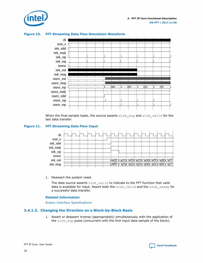
Figure 10. FFT Streaming Data Flow Simulation Waveform
clkreset_n
sink_validsink_ready
sink_sopsink_eop
inversesink_real
sink_imagsource_real
source_imagsource_exp
source_readysource_valid
source_sopsource_eop
EXP0 EXP1 EXP2 EXP3
When the final sample loads, the source asserts sink_eop and sink_valid for thelast data transfer.
Figure 11. FFT Streaming Data Flow Input
clkreset_n
sink_validsink_ready
sink_sopinverse
sink_realsink_imag
xr(0) xr(1) xr(2) xr(3) xr(4) xr(5) xr(6) xr(7)xi(0) xi(1) xi(2) xi(3) xi(4) xi(5) xi(6) xi(7)
1. Deassert the system reset.
The data source asserts sink_valid to indicate to the FFT function that validdata is available for input. Assert both the sink_valid and the sink_ready fora successful data transfer.
Related Information
Avalon Interface Specifications
3.4.1.2. Changing the Direction on a Block-by-Block Basis
1. Assert or deassert inverse (appropriately) simultaneously with the application ofthe sink_sop pulse (concurrent with the first input data sample of the block).
3. FFT IP Core Functional Description
UG-FFT | 2017.11.06
FFT IP Core: User Guide Send Feedback
30
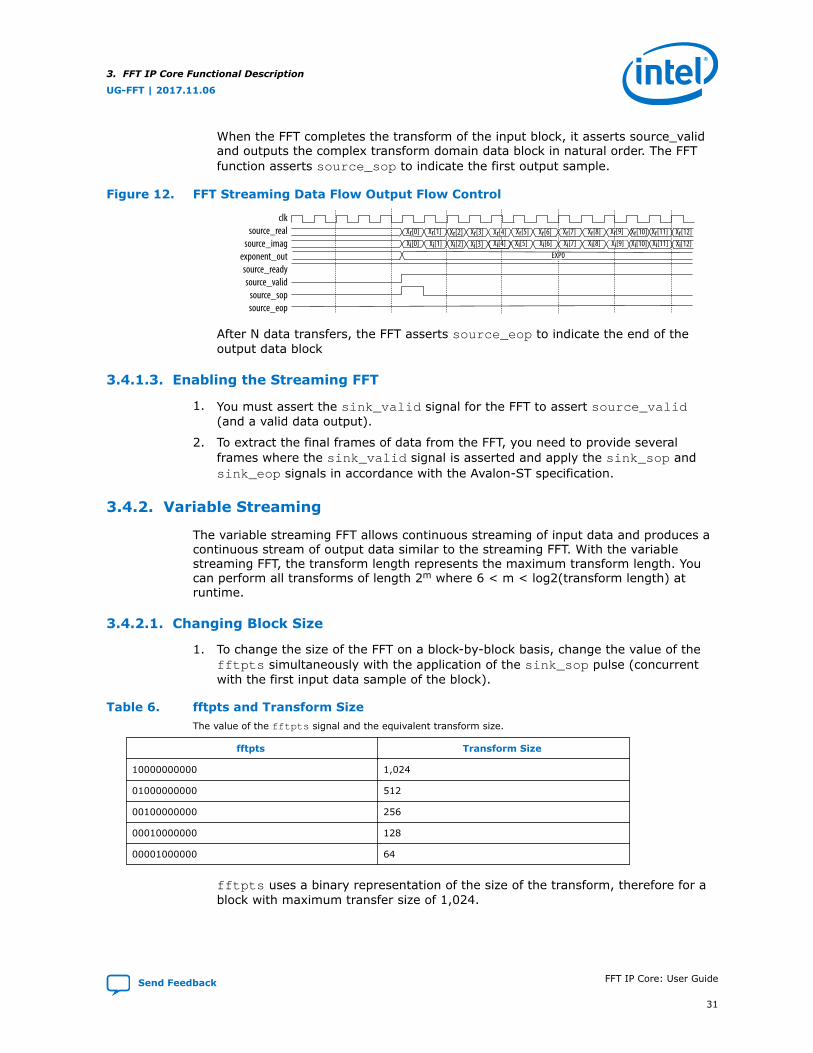
When the FFT completes the transform of the input block, it asserts source_validand outputs the complex transform domain data block in natural order. The FFTfunction asserts source_sop to indicate the first output sample.
Figure 12. FFT Streaming Data Flow Output Flow Control
clksource_real
source_imagexponent_outsource_readysource_valid
source_sopsource_eop
Xr[0] Xr[1] Xr[2] Xr[3] Xr[5] Xr[6] Xr[7] Xr[8] Xr[10] Xr[11] Xr[12]Xr[9]Xi[0] Xi[1] Xi[2] Xi[3] Xi[5] Xi[6] Xi[7] Xi[8] Xi[11] Xi[12]
EXP0Xi[4] Xi[9]Xr[4]
Xi[10]
After N data transfers, the FFT asserts source_eop to indicate the end of theoutput data block
3.4.1.3. Enabling the Streaming FFT
1. You must assert the sink_valid signal for the FFT to assert source_valid(and a valid data output).
2. To extract the final frames of data from the FFT, you need to provide severalframes where the sink_valid signal is asserted and apply the sink_sop andsink_eop signals in accordance with the Avalon-ST specification.
3.4.2. Variable Streaming
The variable streaming FFT allows continuous streaming of input data and produces acontinuous stream of output data similar to the streaming FFT. With the variablestreaming FFT, the transform length represents the maximum transform length. Youcan perform all transforms of length 2m where 6 < m < log2(transform length) atruntime.
3.4.2.1. Changing Block Size
1. To change the size of the FFT on a block-by-block basis, change the value of thefftpts simultaneously with the application of the sink_sop pulse (concurrentwith the first input data sample of the block).
Table 6. fftpts and Transform SizeThe value of the fftpts signal and the equivalent transform size.
fftpts Transform Size
10000000000 1,024
01000000000 512
00100000000 256
00010000000 128
00001000000 64
fftpts uses a binary representation of the size of the transform, therefore for ablock with maximum transfer size of 1,024.
3. FFT IP Core Functional Description
UG-FFT | 2017.11.06
Send Feedback FFT IP Core: User Guide
31

Always drive fftpts_in even if you are not dynamically changing the block size.For a fixed implementation drive it to match the transform length in the parametereditor.
3.4.2.2. Changing Direction
To change direction on a block-by-block basis:
1. Assert or deassert inverse (appropriately) simultaneously with the application ofthe sink_sop pulse (concurrent with the first input data sample of the block).
When the FFT completes the transform of the input block, it assertssource_valid and outputs the complex transform domain data block. The FFTfunction asserts the source_sop to indicate the first output sample. The order ofthe output data depends on the output order that you select in IP Toolbench. Theoutput of the FFT may be in natural order order.
3.4.2.3. I/O Order
The input order allows you to select the order in which you feed the samples to theFFT.
Table 7. Input Order
Order Description
Natural order The FFT requires the order of the input samples to be sequential (1, 2 …, n – 1, n)where n is the size of the current transform.
Digit ReverseOrder
The FFT requires the input samples to be in digit-reversed order.
–N/2 to N/2 The FFT requires the input samples to be in the order –N/2 to (N/2) – 1 (also known asDC-centered order)
Similarly the output order specifies the order in which the FFT generates the output.Whether you can select Bit Reverse Order or Digit Reverse Order depends on yourData Representation (Fixed Point or Floating Point). If you select Fixed Point,the FFT variation implements the radix-22 algorithm and the reverse I/O order optionis Bit Reverse Order. If you select Floating Point, the FFT variation implements themixed radix-4/2 algorithm and the reverse I/O order option is Digit Reverse Order.
For sample digit-reversed order, if n is a power of four, the order is radix-4 digit-reversed order, in which two-bit digits in the sample number are units in the reverseordering. For example, if n = 16, sample number 4 becomes the second sample in thesample stream (by reversal of the digits in 0001, the location in the sample stream, to0100). However, in mixed radix-4/2 algorithm, n need not be a power of four. If n isnot a power of four, the two-bit digits are grouped from the least significant bit, andthe most significant bit becomes the least significant bit in the digit-reversed order.For example, if n = 32, the sample number 18 (10010) in the natural orderingbecomes sample number 17 (10001) in the digit-reversed order.
3.4.2.4. Enabling the Variable Streaming FFT
1. Assert sink_valid.
2. Transfer valid data to the FFT. The FFT processes data.
3. FFT IP Core Functional Description
UG-FFT | 2017.11.06
FFT IP Core: User Guide Send Feedback
32

Example 1. FFT Behavior When sink_valid is Deasserted
Clock
Frame 1 Frame 2
Input Data
The input data stops,but the output continues
Output Data
sink_valid
source_valid
When the FFT is stopped withina frame, the output pauses
1. Deassert sink_valid during a frame to stall the FFT, which then processes nodata until you assert sink_valid. Any previous frames that are still in the FFTalso stall.
2. If you deassert sink_valid between frames, the FFT processes and transfers thedata currently in the FFT to the output.
3. Disable the FFT by deasserting the clk_en signal.
3.4.2.5. Dynamically Changing the FFT Size
The FFT stalls the incoming data (deasserts the sink_ready signal) until all the FFTprocesses and transfers all of the previous FFT frames of the previous FFT size to theoutput.
Figure 13. Dynamically Changing the FFT Size
clockreset_n
sink_validsink_ready
sink_sopsink_eop
inversesink_real
sink_imagsource_real
source_imagsource_ready
source_validsource_sopsource_eop
fftps
1. Change the size of the incoming FFT,
3. FFT IP Core Functional Description
UG-FFT | 2017.11.06
Send Feedback FFT IP Core: User Guide
33

3.4.2.6. I/O Order
The I/O order determines order of samples entering and leaving the FFT and alsodetermines if the FFT is operating in engine-only mode or engine with bit-reversal ordigit-reversal mode.
If the FFT operates in engine-only mode, the output data is available afterapproximately N + latency clocks cycles after the first sample was input to the FFT.Latency represents a small latency through the FFT core and depends on thetransform size. For engine with bit-reversal mode, the output is available afterapproximately 2N + latency cycles.
Figure 14. Data Flow—Engine-Only Mode
clkreset_n
sink_validsink_ready
sink_sopsink_eopsink_real
sink_imagsource_real
source_imagsource_valid
source_sopsource_eop
Figure 15. Data Flow—Engine with Bit-Reversal or Digit-Reversal Mode
clkreset_n
sink_validsink_ready
sink_sopsink_eopsink_real
sink_imagsource_real
source_imagsource_valid
source_sopsource_eop
3.4.3. Buffered Burst
The buffered burst I/O data flow FFT requires fewer memory resources than thestreaming I/O data flow FFT, but the tradeoff is an average block throughputreduction.
3. FFT IP Core Functional Description
UG-FFT | 2017.11.06
FFT IP Core: User Guide Send Feedback
34
3.4.3.1. Enabling the Buffered Burst FFT
Figure 16. FFT Buffered Burst Data Flow Input Flow Control
clkreset_n
sink_validsink_ready
sink_sopinverse
sink_realsink_imag
xr(0) xr(1) xr(2) xr(3) xr(4) xr(5) xr(6) xr(7) xr(8) xr(9)xi(0) xi(1) xi(2) xi(3) xi(4) xi(5) xi(6) xi(7) xi(8) xi(9)
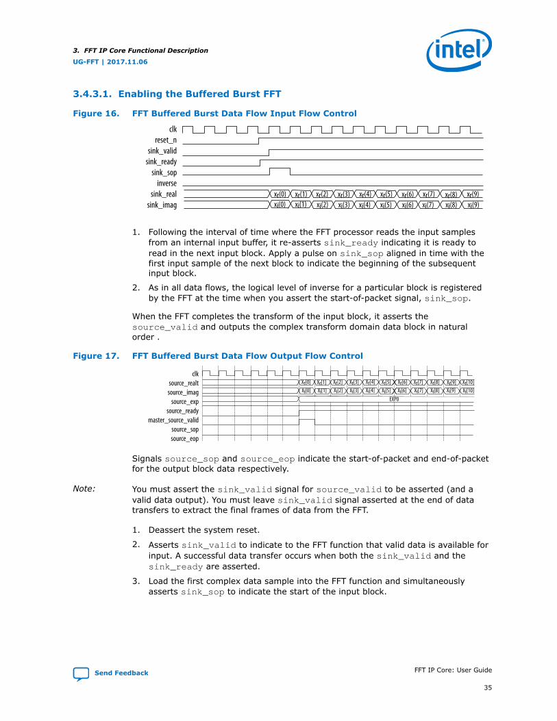
1. Following the interval of time where the FFT processor reads the input samplesfrom an internal input buffer, it re-asserts sink_ready indicating it is ready toread in the next input block. Apply a pulse on sink_sop aligned in time with thefirst input sample of the next block to indicate the beginning of the subsequentinput block.
2. As in all data flows, the logical level of inverse for a particular block is registeredby the FFT at the time when you assert the start-of-packet signal, sink_sop.
When the FFT completes the transform of the input block, it asserts thesource_valid and outputs the complex transform domain data block in naturalorder .
Figure 17. FFT Buffered Burst Data Flow Output Flow Control
clksource_realt
source_imagsource_exp
source_readymaster_source_valid
source_sopsource_eop
EXP0
Xr[0] Xr[1] Xr[2] Xr[3] Xr[4] Xr[5] Xr[6] Xr[7] Xr[8] Xr[9] Xr[10]Xi[0] Xi[1] Xi[2] Xi[3] Xi[4] Xi[5] Xi[6] Xi[7] Xi[8] Xi[9] Xi[10]
Signals source_sop and source_eop indicate the start-of-packet and end-of-packetfor the output block data respectively.
Note: You must assert the sink_valid signal for source_valid to be asserted (and avalid data output). You must leave sink_valid signal asserted at the end of datatransfers to extract the final frames of data from the FFT.
1. Deassert the system reset.
2. Asserts sink_valid to indicate to the FFT function that valid data is available forinput. A successful data transfer occurs when both the sink_valid and thesink_ready are asserted.
3. Load the first complex data sample into the FFT function and simultaneouslyasserts sink_sop to indicate the start of the input block.
3. FFT IP Core Functional Description
UG-FFT | 2017.11.06
Send Feedback FFT IP Core: User Guide
35

4. On the next clock cycle, sink_sop is deasserted and you must load the followingN – 1 complex input data samples in natural order.
5. On the last complex data sample, assert sink_eop.
6. When you load the input block, the FFT function begins computing the transformon the stored input block. Hold the sink_ready signal high as you can transferthe first few samples of the subsequent frame into the small FIFO at the input. Ifthis FIFO buffer is filled, the FFT deasserts the sink_ready signal. It is notmandatory to transfer samples during sink_ready cycles.
Example 2. FFT Buffered Burst Data Flow Simulation Waveform
clkreset_n
sink_validsink_ready
sink_sopsink_eop
inversesink_real
sink_imagsource_real
source_imagsource_exp
source_readysource_valid
source_sopsource_eop
-13609 -47729 271 31221 -21224
-13609 -47729 271 31221 -21224
EXP3EXP2EXP1EXP0
Related Information
Enabling the Streaming FFT on page 31
3.4.4. Burst
The burst I/O data flow FFT operates similarly to the buffered burst FFT, except thatthe burst FFT requires even lower memory resources for a given parameterization atthe expense of reduced average throughput. The following figure shows the simulationresults for the burst FFT. The signals source_valid and sink_ready indicate, tothe system data sources and slave sinks either side of the FFT, when the FFT canaccept a new block of data and when a valid output block is available on the FFToutput.
3. FFT IP Core Functional Description
UG-FFT | 2017.11.06
FFT IP Core: User Guide Send Feedback
36

Figure 18. FFT Burst Data Flow Simulation Waveform
-47729 271
-47729 271
EXP0 EXP1 EXP2
clkreset_n
sink_validsink_ready
sink_sopsink_eop
inversesink_real
sink_imagsource_real
source_imagsource_exp
source_readysource_valid
source_sopsource_eop
In a burst I/O data flow FFT, the FFT can process a single input block only. A smallFIFO buffer at the sink of the block and sink_ready is not deasserted until this FIFObuffer is full. You can provide a small number of additional input samples associatedwith the subsequent input block. You don’t have to provide data to the FFT duringsink_ready cycles. The burst FFT can load the rest of the subsequent FFT frame onlywhen the previous transform is fully unloaded.
Related Information
Enabling the Streaming FFT on page 31
3.5. FFT IP Core Parameters
Table 8. Basic Parameters
Parameter Value Description
Transform Length 64, 128, 256, 512, 1024,2048, 4096, 8192,16384, 32768, or 65536.Variable streaming alsoallows 8, 16, 32,131072, and 262144.
The transform length. For variable streaming, this value is themaximum FFT length.
Transform Direction Forward, reverse,bidirectional
The transform direction.
I/O Data Flow StreamingVariable StreamingBuffered BurstBurst
If you select Variable Streaming and Floating Point, the precisionis automatically set to 32, and the reverse I/O order options areDigit Reverse Order.
I/O Order Bit Reverse Order, DigitReverse Order, NaturalOrder, N/2 to N/2
The input and output order for data entering and leaving the FFT(variable streaming FFT only). The Digit Reverse Order optionreplaces the Bit Reverse Order in variable streaming floatingpoint variations.
Data Representation Fixed point or singlefloating point, or blockfloating point
The internal data representation type (variable streaming FFTonly), either fixed point with natural bit-growth or single precisionfloating point. Floating-point bidirectional IP cores expect input in
continued...
3. FFT IP Core Functional Description
UG-FFT | 2017.11.06
Send Feedback FFT IP Core: User Guide
37
Parameter Value Description
natural order for forward transforms and digit reverse order forreverse transforms. The output order is digit reverse order forforward transforms and natural order for reverse transforms.
Data Width 8, 10, 12, 14, 16, 18, 20,24, 28, 32
The data precision. The values 28 and 32 are available forvariable streaming only.
Twiddle Width 8, 10, 12, 14, 16, 18, 20,24, 28, 32
The twiddle precision. The values 28 and 32 are available forvariable streaming only. Twiddle factor precision must be lessthan or equal to data precision.
The FFT IP core's advanced parameters.
Table 9. Advanced Parameters
Parameter Value Description
FFT Engine Architecture Quad Output, SingleOutput
Choose between one, two, and four quad-output FFT enginesworking in parallel. Alternatively, if you have selected a single-output FFT engine architecture, you may choose to implementone or two engines in parallel. Multiple parallel engines reducetransform time at the expense of device resources, which allowsyou to select the desired area and throughput trade-off point.Not available for variable streaming or streaming FFTs.
Number of Parallel FFT Engines 1, 2, 4
DSP Block Resource Optimization On or Off Turn on for multiplier structure optimizations. These optimizationsuse different DSP block configurations to pack multiply operationsand reduce DSP resource requirements. This optimization mayreduce FMAX because of the structure of the specific configurationsof the DSP blocks when compared to the basic operation.Specifically, on Stratix V devices, this optimization may also comeat the expense of accuracy. You can evaluate it using the MATLABmodel provided and bit wise accurate simulation models. If youturn on DSP Block Resource Optimization and your variationhas data precision between 18 and 25 bits, inclusive, and twiddleprecision less than or equal to 18 bits, the FFT MegaCore functionconfigures the DSP blocks in complex 18 x 25 multiplicationmode.
Enable Hard Floating PointBlocks
On or off For Arria 10 devices and single-floating-point FFTs only.
3.6. FFT IP Core Interfaces and Signals
The FFT IP core uses the Avalon-ST interface. You may achieve a higher clock rate bydriving the source ready signal source_ready of the FFT high, and not connectingthe sink ready signal sink_ready.
The FFT MegaCore function has a READY_LATENCY value of zero.
3.6.1. Avalon-ST Interfaces in DSP IP Cores
Avalon-ST interfaces define a standard, flexible, and modular protocol for datatransfers from a source interface to a sink interface.
The input interface is an Avalon-ST sink and the output interface is an Avalon-STsource. The Avalon-ST interface supports packet transfers with packets interleavedacross multiple channels.
3. FFT IP Core Functional Description
UG-FFT | 2017.11.06
FFT IP Core: User Guide Send Feedback
38

Avalon-ST interface signals can describe traditional streaming interfaces supporting asingle stream of data without knowledge of channels or packet boundaries. Suchinterfaces typically contain data, ready, and valid signals. Avalon-ST interfaces canalso support more complex protocols for burst and packet transfers with packetsinterleaved across multiple channels. The Avalon-ST interface inherently synchronizesmultichannel designs, which allows you to achieve efficient, time-multiplexedimplementations without having to implement complex control logic.
Avalon-ST interfaces support backpressure, which is a flow control mechanism wherea sink can signal to a source to stop sending data. The sink typically usesbackpressure to stop the flow of data when its FIFO buffers are full or when it hascongestion on its output.
Related Information
Avalon Interface Specifications
3.6.2. FFT IP Core Avalon-ST Signals
Table 10. Avalon-ST Signals
Signal Name Direction Avalon-ST Type Size Description
clk Input clk 1 Clock signal that clocks all internal FFT enginecomponents.
reset_n Input reset_n 1 Active-low asynchronous reset signal.This signal canbe asserted asynchronously, but must remainasserted at least one clk clock cycle and must bedeasserted synchronously with clk.
sink_eop Input endofpacket 1 Indicates the end of the incoming FFT frame.
sink_error Input error 2 Indicates an error has occurred in an upstreammodule, because of an illegal usage of the Avalon-STprotocol. The following errors are defined:• 00 = no error• 01 = missing start of packet (SOP)• 10 = missing end of packet (EOP)• 11 = unexpected EOP
If this signal is not used in upstream modules,set to zero.
sink_imag Input data data precisionwidth
Imaginary input data, which represents a signednumber of data precision bits.
sink_ready Output ready 1 Asserted by the FFT engine when it can accept data.It is not mandatory to provide data to the FFT duringready cycles.
sink_real Input data data precisionwidth
Real input data, which represents a signed numberof data precision bits.
sink_sop Input startofpacket 1 Indicates the start of the incoming FFT frame.
sink_valid Input valid 1 Asserted when data on the data bus is valid. Whensink_valid and sink_ready are asserted, a datatransfer takes place..
continued...
3. FFT IP Core Functional Description
UG-FFT | 2017.11.06
Send Feedback FFT IP Core: User Guide
39
Signal Name Direction Avalon-ST Type Size Description
sink_data Input data Variable In Qsys systems, this Avalon-ST-compliant data busincludes all the Avalon-ST input data signals fromMSB to LSB:• sink_real
• sink_imag
• fftpts_in
• inverse
source_eop Output endofpacket 1 Marks the end of the outgoing FFT frame. Only validwhen source_valid is asserted.
source_error Output error 2 Indicates an error has occurred either in anupstream module or within the FFT module (logicalOR of sink_error with errors generated in theFFT).
source_exp Output data 6 Streaming, burst, and buffered burst FFTs only.Signed block exponent: Accounts for scaling ofinternal signal values during FFT computation.
source_imag Output data (data precisionwidth + growth)
Imaginary output data. For burst, buffered burst,streaming, and variable streaming floating pointFFTs, the output data width is equal to the input datawidth. For variable streaming fixed point FFTs, thesize of the output data is dependent on the numberof stages defined for the FFT and is 2 bits per radix22 stage.
source_ready Input ready 1 Asserted by the downstream module if it is able toaccept data.
source_real Output data (data precisionwidth + growth)
Real output data. For burst, buffered burst,streaming, and variable streaming floating pointFFTs, the output data width is equal to the input datawidth. For variable streaming fixed point FFTs, thesize of the output data is dependent on the numberof stages defined for the FFT and is 2 bits per radix22 stage. Variable streaming fixed point FFT only.Growth is log2(N)+1.
source_sop Output startofpacket 1 Marks the start of the outgoing FFT frame. Only validwhen source_valid is asserted.
source_valid Output valid 1 Asserted by the FFT when there is valid data tooutput.
source_data Output data Variable In Qsys systems, this Avalon-ST-compliant data busincludes all the Avalon-ST output data signals fromMSB to LSB:• source_real
• source_imag
• fftpts_out
Related Information
• Avalon Streaming Interface Specification
• Recommended Design Practices
3.6.2.1. Component Specific Signals
The component specific signals.
3. FFT IP Core Functional Description
UG-FFT | 2017.11.06
FFT IP Core: User Guide Send Feedback
40

Table 11. Component Specific Signals
Signal Name Direction Size Description
fftpts_in Input log2(maximumnumber of points)
The number of points in this FFT frame. If you do not specify this value, theFFT can not be a variable length. The default behavior is for the FFT to havefixed length of maximum points. Only sampled at SOP. Always drivefftpts_in even if you are not dynamically changing the block size. For afixed implementation drive it to match the transform length in the parametereditor.
fftpts_out Output log2(maximumnumber of points)
The number of points in this FFT frame synchronized to the Avalon-ST sourceinterface. Variable streaming only.
inverse Input 1 Inverse FFT calculated if asserted. Only sampled at SOP.
Incorrect usage of the Avalon-ST interface protocol on the sink interface results in aerror on source_error. Table 3–8 defines the behavior of the FFT when an incorrectAvalon-ST transfer is detected. If an error occurs, the behavior of the FFT is undefinedand you must reset the FFT with reset_n.
Table 12. Error Handling Behavior
Error source_error Description
Missing SOP 01 Asserted when valid goes high, but there is no start of frame.
Missing EOP 10 Asserted if the FFT accepts N valid samples of an FFT frame, but there is no EOP signal.
Unexpected EOP 11 Asserted if EOP is asserted before N valid samples are accepted.
3. FFT IP Core Functional Description
UG-FFT | 2017.11.06
Send Feedback FFT IP Core: User Guide
41
4. Block Floating Point ScalingBlock-floating-point (BFP) scaling is a trade-off between fixed-point and full floating-point FFTs.
In fixed-point FFTs, the data precision needs to be large enough to adequatelyrepresent all intermediate values throughout the transform computation. For large FFTtransform sizes, an FFT fixed-point implementation that allows for word growth canmake either the data width excessive or can lead to a loss of precision.
Floating-point FFTs represents each number as a mantissa with an individualexponent. The improved precision is offset by demand for increased device resources.
In a block-floating point FFT, all of the values have an independent mantissa but sharea common exponent in each data block. Data is input to the FFT function as fixedpoint complex numbers (even though the exponent is effectively 0, you do not enteran exponent).
The block-floating point FFT ensures full use of the data width within the FFT functionand throughout the transform. After every pass through a radix-4 FFT, the data widthmay grow up to log2 (42) = 2.5 bits. The data scales according to a measure of theblock dynamic range on the output of the previous pass. The FFT accumulates thenumber of shifts and then outputs them as an exponent for the entire block. Thisshifting ensures that the minimum of least significant bits (LSBs) are discarded priorto the rounding of the post-multiplication output. In effect, the block-floating pointrepresentation is as a digital automatic gain control. To yield uniform scaling acrosssuccessive output blocks, you must scale the FFT function output by the finalexponent.
In comparing the block-floating point output of the FFT MegaCore function to theoutput of a full precision FFT from a tool like MATLAB, you must scale the output by 2(–exponent_out) to account for the discarded LSBs during the transform.
Unlike an FFT block that uses floating point arithmetic, a block-floating-point FFT blockdoes not provide an input for exponents. Internally, the IP core represents a complexvalue integer pair with a single scale factor that it typically shares among othercomplex value integer pairs. After each stage of the FFT, the IP core detects thelargest output value and scales the intermediate result to improve the precision. Theexponent records the number of left or right shifts to perform the scaling. As a result,the output magnitude relative to the input level is:
output*2-exponent
For example, if exponent = –3, the input samples are shifted right by three bits, andhence the magnitude of the output is output*23.
UG-FFT | 2017.11.06
Send Feedback
Intel Corporation. All rights reserved. Agilex, Altera, Arria, Cyclone, Enpirion, Intel, the Intel logo, MAX, Nios,Quartus and Stratix words and logos are trademarks of Intel Corporation or its subsidiaries in the U.S. and/orother countries. Intel warrants performance of its FPGA and semiconductor products to current specifications inaccordance with Intel's standard warranty, but reserves the right to make changes to any products and servicesat any time without notice. Intel assumes no responsibility or liability arising out of the application or use of anyinformation, product, or service described herein except as expressly agreed to in writing by Intel. Intelcustomers are advised to obtain the latest version of device specifications before relying on any publishedinformation and before placing orders for products or services.*Other names and brands may be claimed as the property of others.
ISO9001:2015Registered
After every pass through a radix-2 or radix-4 engine in the FFT core, the addition andmultiplication operations cause the data bits width to grow. In other words, the totaldata bits width from the FFT operation grows proportionally to the number of passes.The number of passes of the FFT/IFFT computation depends on the logarithm of thenumber of points.
A fixed-point FFT needs a huge multiplier and memory block to accommodate thelarge bit width growth to represent the high dynamic range. Though floating-point ispowerful in arithmetic operations, its power comes at the cost of higher designcomplexity such as a floating-point multiplier and a floating-point adder. BFParithmetic combines the advantages of floating-point and fixed-point arithmetic. BFParithmetic offers a better signal-to-noise ratio (SNR) and dynamic range than doesfloating-point and fixed-point arithmetic with the same number of bits in the hardwareimplementation.
In a block-floating-point FFT, the radix-2 or radix-4 computation of each pass sharesthe same hardware, the IP core reads the data from memory, passes ti through theengine, and writtes back to memory. Before entering the next pass, the IP core shiftseach data sample right (an operation called "scaling") if the addition and multiplicationoperations produce a carry-out bit. The IP core bases the number of bits that it shiftson the difference in bit growth between the data sample and the maximum datasample it detect in the previous stage. The IP core records the maximum bit growth inthe exponent register. Each data sample now shares the same exponent value anddata bit width to go to the next core engine. You can reuse the same core enginewithout incurring the expense of a larger engine to accommodate the bit growth.
The output SNR depends on how many bits of right shift occur and at what stages ofthe radix core computation they occur. Tthat the signal-to-noise ratio is datadependent and you need to know the input signal to compute the SNR.
4.1. Possible Exponent Values
Depending on the length of the FFT/IFFT, the number of passes through the radixengine is known and therefore the range of the exponent is known. The possiblevalues of the exponent are determined by the following equations:
P = ceil{log4N}, where N is the transform length
R = 0 if log2N is even, otherwise R = 1
Single output range = (–3P+R, P+R–4)
Quad output range = (–3P+R+1, P+R–7)
These equations translate to the values in Table A–1.
Table 13. Exponent Scaling Values for FFT / IFFT (1)
N P Single Output Engine Quad Output Engine
Max (2) Min (2) Max (2) Min (2)
64 3 –9 –1 –8 –4
128 4 –11 1 –10 –2
256 4 –12 0 –11 –3
continued...
4. Block Floating Point Scaling
UG-FFT | 2017.11.06
Send Feedback FFT IP Core: User Guide
43

N P Single Output Engine Quad Output Engine
Max (2) Min (2) Max (2) Min (2)
512 5 –14 2 –13 –1
1,024 5 –15 1 –14 –2
2,048 6 –17 3 –16 0
4,096 6 –18 2 –17 –1
8,192 7 –20 4 –19 1
16,384 7 –21 3 –20 0
Note to Table A–1:1. This table lists the range of exponents, which is the number of scale events that occurred internally.
For IFFT, the output must be divided by N externally. If more arithmetic operations are performedafter this step, the division by N must be performed at the end to prevent loss of precision.
2. The maximum and minimum values show the number of times the data is shifted. A negative valueindicates shifts to the left, while a positive value indicates shifts to the right.
4.2. Implementing Scaling
To implement the scaling algorithm, follow these steps:
1. Determine the length of the resulting full scale dynamic range storage register. Toget the length, add the width of the data to the number of times the data isshifted. For example, for a 16-bit data, 256-point Quad Output FFT/IFFT with Max= –11 and Min = –3. The Max value indicates 11 shifts to the left, so the resultingfull scaled data width is 16 + 11, or 27 bits.
2. Map the output data to the appropriate location within the expanded dynamicrange register based upon the exponent value. To continue the above example,the 16-bit output data [15..0] from the FFT/IFFT is mapped to [26..11] for anexponent of –11, to [25..10] for an exponent of –10, to [24..9] for an exponent of–9, and so on.
3. Sign extend the data within the full scale register.
4.2.1. Example of Scaling
A sample of Verilog HDL code that illustrates the scaling of the output data (forexponents –11 to –9) with sign extension is shown in the following example:
case (exp) 6'b110101 : //-11 Set data equal to MSBs begin full_range_real_out[26:0] <= {real_in[15:0],11'b0}; full_range_imag_out[26:0] <= {imag_in[15:0],11'b0}; end 6'b110110 : //-10 Equals left shift by 10 with sign extension begin full_range_real_out[26] <= {real_in[15]}; full_range_real_out[25:0] <= {real_in[15:0],10'b0};
4. Block Floating Point Scaling
UG-FFT | 2017.11.06
FFT IP Core: User Guide Send Feedback
44
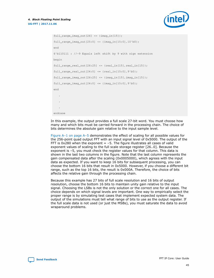
full_range_imag_out[26] <= {imag_in[15]}; full_range_imag_out[25:0] <= {imag_in[15:0],10'b0}; end 6'b110111 : //-9 Equals left shift by 9 with sign extension begin full_range_real_out[26:25] <= {real_in[15],real_in[15]}; full_range_real_out[24:0] <= {real_in[15:0],9'b0}; full_range_imag_out[26:25] <= {imag_in[15],imag_in[15]}; full_range_imag_out[24:0] <= {imag_in[15:0],9'b0}; end
.
.
.
endcase
In this example, the output provides a full scale 27-bit word. You must choose howmany and which bits must be carried forward in the processing chain. The choice ofbits determines the absolute gain relative to the input sample level.
Figure A–1 on page A–5 demonstrates the effect of scaling for all possible values forthe 256-point quad output FFT with an input signal level of 0x5000. The output of theFFT is 0x280 when the exponent = –5. The figure illustrates all cases of validexponent values of scaling to the full scale storage register [26..0]. Because theexponent is –5, you must check the register values for that column. This data isshown in the last two columns in the figure. Note that the last column represents thegain compensated data after the scaling (0x0005000), which agrees with the inputdata as expected. If you want to keep 16 bits for subsequent processing, you canchoose the bottom 16 bits that result in 0x5000. However, if you choose a different bitrange, such as the top 16 bits, the result is 0x000A. Therefore, the choice of bitsaffects the relative gain through the processing chain.
Because this example has 27 bits of full scale resolution and 16 bits of outputresolution, choose the bottom 16 bits to maintain unity gain relative to the inputsignal. Choosing the LSBs is not the only solution or the correct one for all cases. Thechoice depends on which signal levels are important. One way to empirically select theproper range is by simulating test cases that implement expected system data. Theoutput of the simulations must tell what range of bits to use as the output register. Ifthe full scale data is not used (or just the MSBs), you must saturate the data to avoidwraparound problems.
4. Block Floating Point Scaling
UG-FFT | 2017.11.06
Send Feedback FFT IP Core: User Guide
45

Figure 19. Scaling of Input Data Sample = 0x5000
4.3. Unity Gain in an IFFT+FFT Pair
Given sufficiently high precision, such as with floating-point arithmetic, in theory youcan obtain unity gain when you cascade an IFFT and FFT. However, in BFP arithmetic,pay special attention to the exponent values of the IFFT/FFT blocks to achieve theunity gain. This section explains the steps to derive a unity gain output from anIFFT/FFT IP Core pair, using BFP arithmetic.
BFP arithmetic does not provide an input for the exponent, so you must keep track ofthe exponent from the IFFT block if you are feeding the output to the FFT blockimmediately thereafter and divide by N at the end to acquire the original signalmagnitude.
4. Block Floating Point Scaling
UG-FFT | 2017.11.06
FFT IP Core: User Guide Send Feedback
46
Figure 20. Derivation to Achieve IFFT/FFT Pair Unity Gain
IFFT
x0 X0 = IFFT(x0)
= N1
× IFFTa (x0)
= N1
× data1 × 2 –exp1
FFT
x0 = FFT(X0)
= FFT(N1
× data1 × 2 –exp1 )
= N1
× 2–exp1 × FFTa (data1)
= N1
× 2–exp1 × data2 × 2 –exp2
= N1
× 2 –exp2–exp1 × data2
where:
x0 = Input data to IFFT
X0 = Output data from IFFT
N = number of points
data1 = IFFT output data and FFT input data
data2 = FFT output data
exp1 = IFFT output exponent
exp2 = FFT output exponent
IFFTa = IFFT
FFTa = FFT
Any scaling operation on X0 followed by truncation loses the value of exp1 and doesnot result in unity gain at x0. Any scaling operation must be done on X0 only when itis the final result. If the intermediate result X0 is first padded with exp1 number ofzeros and then truncated or if the data bits of X0 are truncated, the scalinginformation is lost.
To keep unity gain, you can pas the exp1 value to the output of the FFT block.Alternatively, preserve the full precision of data1×2–exp1 and use this value as inputto the FFT block. The second method requires a large size for the FFT to accept theinput with growing bit width from IFFT operations. The resolution required toaccommodate this bit width in most cases, exceeds the maximum data widthsupported by the IP core.
Related Information
Achieving Unity Gain in Block Floating Point IFFT+FFT Pair design example
4. Block Floating Point Scaling
UG-FFT | 2017.11.06
Send Feedback FFT IP Core: User Guide
47

5. Document Revision HistoryFFT IP Core User Guide revision history.
Date Version Changes
2018.05.31 17.1 • Corrected the statement: "The IP asserts both the sink_valid and the sink_ready fora successful data transfer."
• Corrected 2m to 2m
2017.11.06 17.1 • Added support for Intel Cyclone 10 devices.• Removed bit-reversed option.• Removed input and output orders topic.
2017.01.14 16.1.1 • Removed DC centred option from variable streaming input and output optionorders.
• Removed product ID and vendor ID codes.
2016.11.11 16.1 Added note about fftpts signal.
2016.08.01 16.1S10 Added support for Stratix 10 devices
2016.05.01 16.0 Added MATLAB simulation flow.
2015.10.01 15.1 Added more info to sink_data and source_data signals
2014.12.15 14.1 • Added more detail to source_data and sink_data signal descriptions.• Added hard-floating point option for Arria 10 devices in the Complex Multiplier
Options• Reworded DSP Block Resource Optimization description• Added block floating point option in parameters table.• Reordered parameters in parameters table.• Removed the following parameters:
— Twiddle ROM Distribution— Use M-RAM or M144K blocks— Implement appropriate logic functions in RAM— Structure— Implement Multipliers in— Global enable clock signal
• Removed Stratix V devices only comment for DSP Resource Optimizationparameter.
• Added final support for Arria 10 and MAX 10 devices
August 2014 14.0 Arria 10Edition
• Added support for Arria 10 devices.• Added new source_data bus description.• Added Arria 10 generated files description.• Removed table with generated file descriptions.• Removed clk_ena
continued...
UG-FFT | 2017.11.06
Send Feedback
Intel Corporation. All rights reserved. Agilex, Altera, Arria, Cyclone, Enpirion, Intel, the Intel logo, MAX, Nios,Quartus and Stratix words and logos are trademarks of Intel Corporation or its subsidiaries in the U.S. and/orother countries. Intel warrants performance of its FPGA and semiconductor products to current specifications inaccordance with Intel's standard warranty, but reserves the right to make changes to any products and servicesat any time without notice. Intel assumes no responsibility or liability arising out of the application or use of anyinformation, product, or service described herein except as expressly agreed to in writing by Intel. Intelcustomers are advised to obtain the latest version of device specifications before relying on any publishedinformation and before placing orders for products or services.*Other names and brands may be claimed as the property of others.
ISO9001:2015Registered

Date Version Changes
June 2014 14.0 • Removed Cyclone III and Stratix III device support• Added support for MAX 10 FPGAs.• Added instructions for using IP Catalog
November2013
13.1 • Added more information to variable streaming I/O dataflow.• Removed device support for following devices:• — HardCopy II, HardCopy III, HardCopy IV E, HardCopy IV GX
— Stratix, Stratix GX, Stratix II, Stratix II GX— Cyclone, Cyclone II— Arria GX
November2012
12.1 Added support for Arria V GZ devices.
5. Document Revision History
UG-FFT | 2017.11.06
Send Feedback FFT IP Core: User Guide
49

A. FFT IP Core User Guide Document ArchiveIf an IP core version is not listed, the user guide for the previous IP core version applies.
IP Core Version User Guide
16.1 FFT IP Core User Guide
15.1 FFT IP Core User Guide
15.0 FFT IP Core User Guide
14.1 FFT IP Core User Guide
UG-FFT | 2017.11.06
Send Feedback
Intel Corporation. All rights reserved. Agilex, Altera, Arria, Cyclone, Enpirion, Intel, the Intel logo, MAX, Nios,Quartus and Stratix words and logos are trademarks of Intel Corporation or its subsidiaries in the U.S. and/orother countries. Intel warrants performance of its FPGA and semiconductor products to current specifications inaccordance with Intel's standard warranty, but reserves the right to make changes to any products and servicesat any time without notice. Intel assumes no responsibility or liability arising out of the application or use of anyinformation, product, or service described herein except as expressly agreed to in writing by Intel. Intelcustomers are advised to obtain the latest version of device specifications before relying on any publishedinformation and before placing orders for products or services.*Other names and brands may be claimed as the property of others.
ISO9001:2015Registered
Top Related