


Languages
Pages
Legal

Appl. Sci. 2014, 4, 305-317; doi:10.3390/app4020305
applied sciences ISSN 2076-3417
www.mdpi.com/journal/applsci
Article
Electrical Properties of Graphene for Interconnect Applications
Antonio Maffucci 1,2,* and Giovanni Miano 3
1 Department of Electrical and Information Engineering, University of Cassino and Southern Lazio,
via G. Di Biasio 43, Cassino 03043, Italy 2 INFN–LNF, Frascati National Laboratory, National Institute of Nuclear Physics, via E. Fermi 40,
Frascati 00044, Italy 3 Department of Electrical Engineering and Information Technology, University Federico II of Naples,
via Claudio 21, Napoli 80125, Italy; E-Mail: [email protected]
* Author to whom correspondence should be addressed; E-Mail: [email protected];
Tel.: +39-0776-299-3691; Fax: +39-0776-299-3707.
Received: 23 March 2014; in revised form: 14 May 2014 / Accepted: 14 May 2014 /
Published: 30 May 2014
Abstract: A semi-classical electrodynamical model is derived to describe the electrical
transport along graphene, based on the modified Boltzmann transport equation. The model
is derived in the typical operating conditions predicted for future integrated circuits
nano-interconnects, i.e., a low bias condition and an operating frequency up to 1 THz.
A generalized non-local dispersive Ohm’s law is derived, which can be regarded as the
constitutive equation for the material. The behavior of the electrical conductivity is
studied with reference to a 2D case (the infinite graphene layer) and a 1D case
(the graphene nanoribbons). The modulation effects of the nanoribbons’ size and chirality
are highlighted, as well as the spatial dispersion introduced in the 2D case by the dyadic
nature of the conductivity.
Keywords: graphene; graphene nanoribbons; nano-interconnects
1. Introduction
Due to their outstanding physical properties, graphene and its allotropes (carbon nanotubes (CNTs)
and graphene nanoribbons (GNRs)) are the major candidates to become the silicon of the 21st century
and open the era of so-called carbon electronics [1,2].
OPEN ACCESS
Appl. Sci. 2014, 4 306
Amongst all such applications, the low electrical resistivity, high thermal conductivity, high current
carrying capability, besides other excellent mechanical properties, make graphene a serious candidate to
replace conventional materials in realizing VLSI nano-interconnects [3,4]. A carbon-based VLSI
technology is not yet a pure theoretical wish, since in the last few years, the rapid progress in graphene
fabrication made possible the first examples of real-world applications. The works [5,6] present high
frequency CMOS oscillators integrating CNT or GNR interconnects, whereas [7] shows the first example
of a computer with PMOS transistors entirely made of CNTs. Carbon nanotubes or graphene interconnects
are also successfully integrated into innovative organic transistors for flexible plastic electronics [8].
The increasing interest in carbon nano-interconnects leads to the quest for more and more accurate
and reliable models, able to include all the quantum effects arising at the nanoscale. This topic has
been given great attention by the recent literature, which presented several modeling approaches, like
phenomenological [9] and semi-classical ones [10]. Based on such models, many papers predicted that
carbon materials could outperform copper for IC on-chip interconnects and vias [11–16].
In the typical working conditions of nano-interconnects, namely a frequency up to THz and low
bias conditions, such nano-structures do not exhibit tunneling transport. Thus, the electrodynamics
may be studied by using a semi-classical description of the electron transport. This leads to the
derivation of a constitutive relation between the electrical field and the density of the current in the
form of a generalization of the classical Ohm’s law, introducing non-local interactions and dispersion.
By coupling such a relation to Maxwell equations, it is possible to derive a generalized transmission
line model for such nano-interconnects. This approach has been followed by the authors to model
isolated metallic CNTs in [16], CNTs with arbitrary radius and chirality in [17,18], multi-walled
CNTs [19] and GNRs [20]. The semi-classical model gives results consistent with those provided by
an alternative hydrodynamic model [21].
In this paper, a comprehensive and self-consistent analysis of the electrical properties of graphene is
presented, with special emphasis on its application as an innovative material for nano-interconnects.
The self-consistency is guaranteed by the fact that the used transport model is derived from an
electrodynamical model described in terms of physically meaningful parameters. This differs from
what can be obtained by means of heuristics approaches. In particular, a self-consistent model provides
a clear analytical relation between the model parameters and the physical and geometrical properties of
the investigated structure. The considered frequency range of applications is limited to values up to 1 THz,
and the operational conditions fall into the low bias regime (the longitudinal electric field along the
interconnect should be Ez < 0.54 V/μm). For such cases, interband transitions are absent and non-linear
effects are negligible, and thus, a simple linear transport of the conducting electrons (π-electrons) may
be derived based on the tight-binding model and the semi-classical Boltzmann equation.
Section 2 is devoted to a brief résumé of the main properties of the band structure for a graphene
sheet and for a graphene nanoribbon. In Section 3, the transport model is presented, derived from a
semi-classical model based on the linearized Boltzmann transport equation. The model leads to the
constitutive relation for the graphene, written in terms of a generalized non-local Ohm’s law in the
frequency and wave-number domain. Section 4 presents a detailed discussion about the properties of
the electrical conductivity, which, in general, results in being a dyad.
Appl. Sci. 2014, 4 307
2. Band Structure
In this chapter, we briefly summarize the main features of the band structure, first for an infinite
graphene layer (a 2D structure) and, then, for the graphene nanoribbon (a 1D structure).
2.1. Graphene Layer
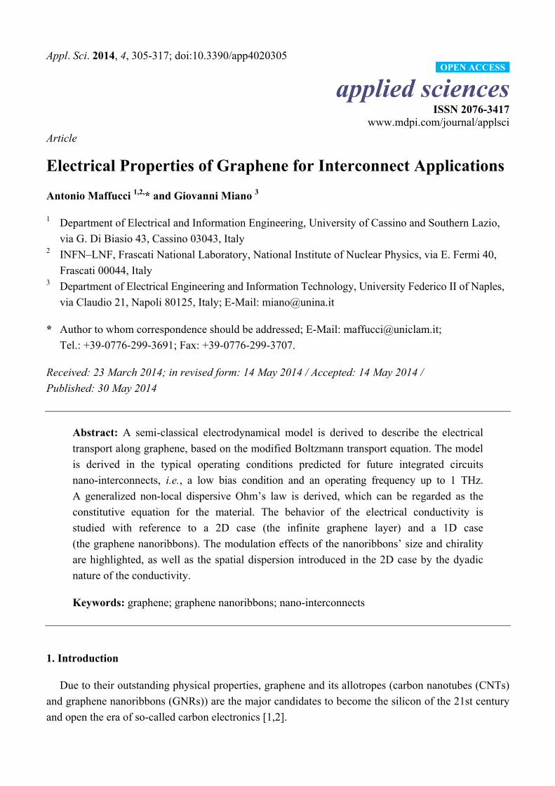
Figure 1a shows the Bravais lattice of the graphene. The unit cell, Sg, is spanned by the two vectors,
a1 and a2, and contains two carbon atoms. The basis vectors (a1,a2) have the same length,
ba 321 aa , and form an angle of π/3, where b = 1.42 Å is the interatomic distance. The
components of the vectors, a1 and a2, with respect to the rectangular coordinate system, (0,x,y) are,
respectively, 3a0 / 2,a0 / 2 and 3a0 / 2,a0 / 2 . The area of the unit cell, Sg, is 2/3 20aAg .
Figure 1. The structure of graphene. (a) Bravais lattice; (b) reciprocal lattice.
In the reciprocal k-space depicted in Figure 1b, the graphene is characterized by the unit cell, ∑g, spanned by the two vectors, b1 and b2, which have the same length 0021 34 ab bb and form
an angle of 2π/3. The components of the vectors, b1 and b2, with respect to the rectangular coordinate system (Q,Kx,ky) are, respectively, 2 / 3a0,2 / a0 and 2 / 3a0,2 / a0 . The area of the unit cell,
∑g, is .38 20
2 aBg The basis vectors of the direct space (a1,a2) and the basis vectors of the
reciprocal space (b1,b2) are related by ai·bj = 2πδij with i,j = 1,2 and the areas, Ag and Bg, are related by
AgBg = (2π)2.
The graphene possesses four valence electrons for each carbon atom. Three of these (the so-called
σ-electrons) form tight bonds with the neighboring atoms in the plane and do not play a part in the
conduction phenomenon. The fourth electron (the so-called π-electron), instead, may move freely
between the positive ions of the lattice.
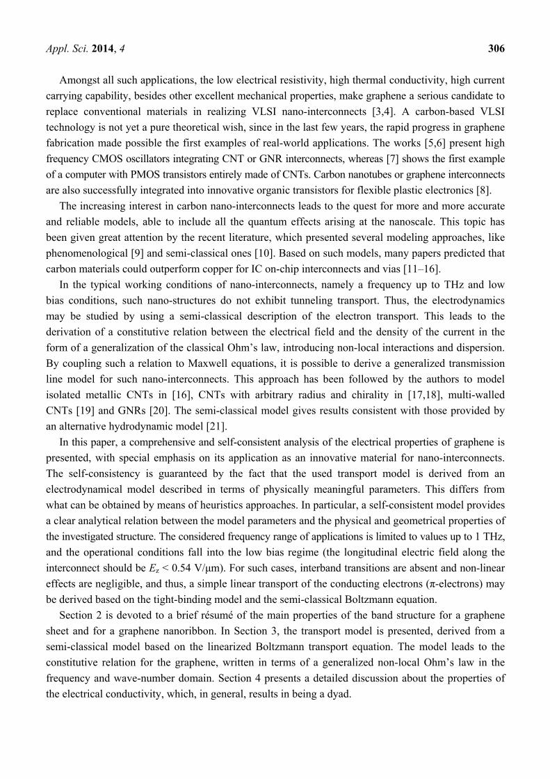
In the nearest-neighbors tight-binding approximation, the π-electrons energy dispersion relation is
(1)
2cos4
2cos
2
3cos41)(
2/10200)(
akakak
Eyyxk
Sg
Appl. Sci. 2014, 4 308
where E(±) denotes the energy, the + sign denotes the conduction band, the − sign denotes the valence
band and γ = 2.7 eV is the carbon-carbon interaction energy. The electronic band structure is depicted
in Figure 2: the valence and conduction bands touch each other at the six vertices of each unit cell,
the so-called Fermi points. In the neighborhood of each Fermi point, the energy dispersion relation
may be approximated as:
(2)
where k0 is the wavenumber at a Fermi point, νF ≈ 0.87 × 10⁶ m/s is the Fermi velocity of the
π-electrons and is the Planck constant.
Figure 2. Graphene electronic band structure. Inset: the neighborhood of a Fermi point.
In the ground state, the valence band of the graphene is completely filled by the π-electrons.
In general, at equilibrium, the energy distribution function of π-electrons is given by the
Dirac–Fermi function:
1
1
0)( /
)(
TkE Be
EF (3)
where kB is the Boltzmann constant and T0 is the graphene absolute temperature, the electrochemical
potential of the graphene being null valued. The distribution function differs from the ideal distribution
function F[E(±)] = u[−E(±)], where u = u(x) is the Heaviside function, only in a region of order kBT0
around the point E(±) = 0; at room temperature, it results eV02.00 TkB .
2.2. Graphene Nanoribbons
Let us now discuss the so-called graphene nanoribbons (GNRs), i.e., ribbons obtained by cutting a
graphene layer, characterized by a high aspect-ratio, namely a transverse width, w, much smaller than
the longitudinal ribbon length. Figure 3 shows the two basic shapes for GNRs, namely nanoribbons
with armchair edges and nanoribbons with zigzag edges (e.g., [20]). These edges have a 30° difference
in their orientation within the graphene sheet. We assume that all dangling bonds at graphene edges are
terminated by hydrogen atoms and, thus, do not contribute to the electronic states near the Fermi level.
In the following, we will assume the Fermi energy to be zero. However, this level may move to values
such as 0.2–0.4 eV, considering the interactions at the GNR/substrate interface.
0
)( kk FvE
Appl. Sci. 2014, 4 309
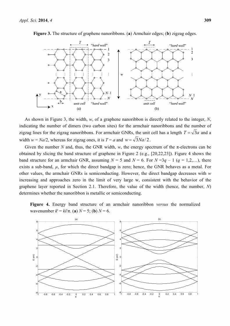
Figure 3. The structure of graphene nanoribbons. (a) Armchair edges; (b) zigzag edges.
As shown in Figure 3, the width, w, of a graphene nanoribbon is directly related to the integer, N,
indicating the number of dimers (two carbon sites) for the armchair nanoribbons and the number of
zigzag lines for the zigzag nanoribbons. For armchair GNRs, the unit cell has a length aT 3 and a
width w = Na/2, whereas for zigzag ones, it is T = a and 2/3Naw .
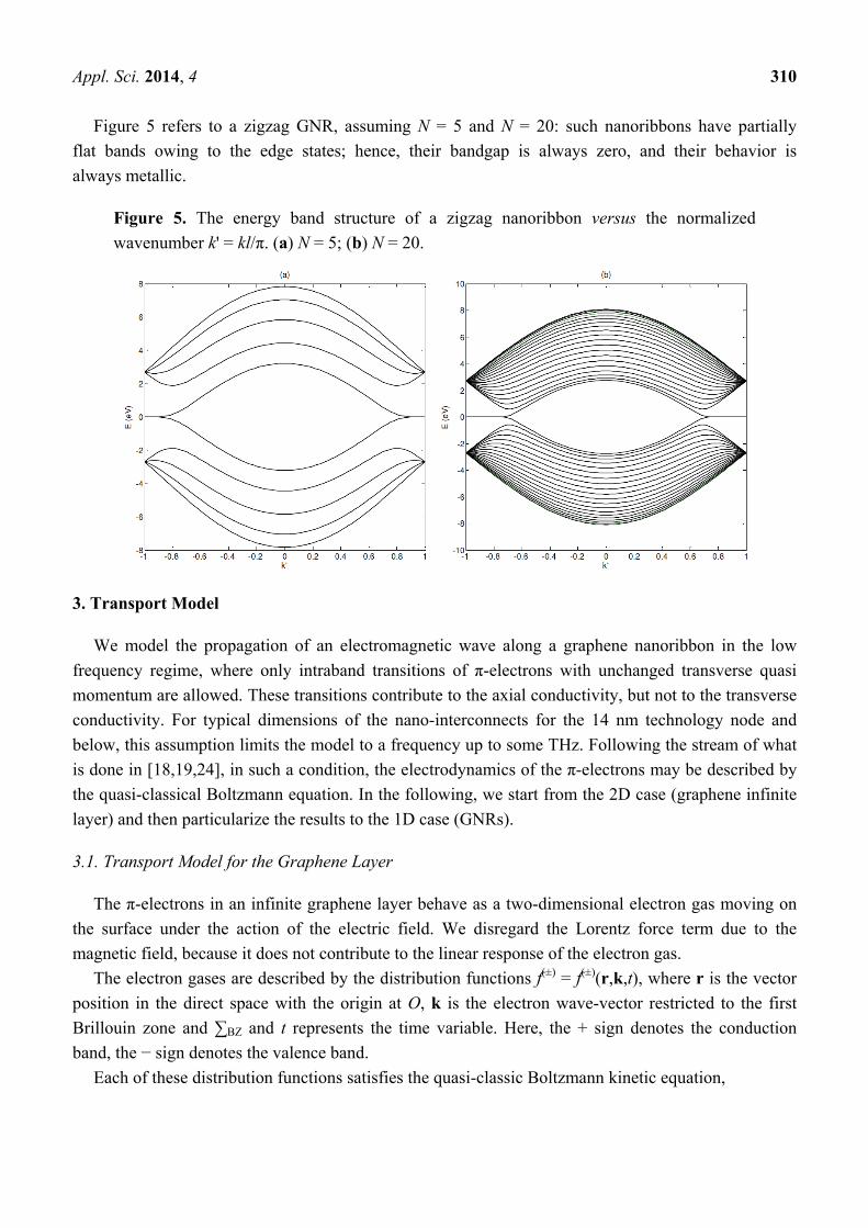
Given the number N and, thus, the GNR width, w, the energy spectrum of the π-electrons can be
obtained by slicing the band structure of graphene in Figure 2 (e.g., [20,22,23]). Figure 4 shows the
band structure for an armchair GNR, assuming N = 5 and N = 6. For N =3q – 1 (q = 1,2,…), there
exists a sub-band, µ, for which the direct bandgap is zero; hence, the GNR behaves as a metal. For
other values, the armchair GNRs is semiconducting. However, the direct bandgap decreases with w
increasing and approaches zero in the limit of very large w, consistent with the behavior of the
graphene layer reported in Section 2.1. Therefore, the value of the width (hence, the number, N)
determines whether the nanoribbon is metallic or semiconducting.
Figure 4. Energy band structure of an armchair nanoribbon versus the normalized
wavenumber k' = kl/π. (a) N = 5; (b) N = 6.
-1 -0.8 -0.6 -0.4 -0.2 0 0.2 0.4 0.6 0.8 1
-8
-6
-4
-2
0
2
4
6
8(a)
k'
E (
eV
)
-1 -0.8 -0.6 -0.4 -0.2 0 0.2 0.4 0.6 0.8 1-8
-6
-4
-2
0
2
4
6
8(b)
k'
E (
eV
)
x
Appl. Sci. 2014, 4 310
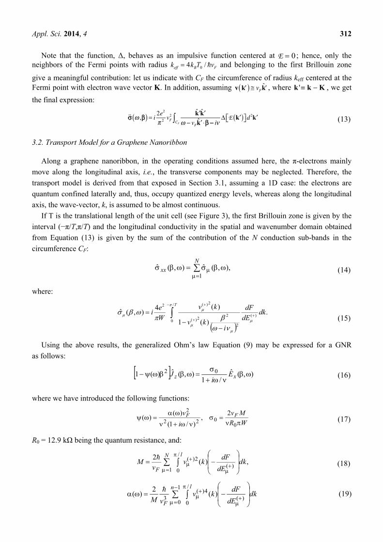
Figure 5 refers to a zigzag GNR, assuming N = 5 and N = 20: such nanoribbons have partially
flat bands owing to the edge states; hence, their bandgap is always zero, and their behavior is
always metallic.
Figure 5. The energy band structure of a zigzag nanoribbon versus the normalized
wavenumber k' = kl/π. (a) N = 5; (b) N = 20.
3. Transport Model
We model the propagation of an electromagnetic wave along a graphene nanoribbon in the low
frequency regime, where only intraband transitions of π-electrons with unchanged transverse quasi
momentum are allowed. These transitions contribute to the axial conductivity, but not to the transverse
conductivity. For typical dimensions of the nano-interconnects for the 14 nm technology node and
below, this assumption limits the model to a frequency up to some THz. Following the stream of what
is done in [18,19,24], in such a condition, the electrodynamics of the π-electrons may be described by
the quasi-classical Boltzmann equation. In the following, we start from the 2D case (graphene infinite
layer) and then particularize the results to the 1D case (GNRs).
3.1. Transport Model for the Graphene Layer
The π-electrons in an infinite graphene layer behave as a two-dimensional electron gas moving on
the surface under the action of the electric field. We disregard the Lorentz force term due to the
magnetic field, because it does not contribute to the linear response of the electron gas.
The electron gases are described by the distribution functions f(±) = f(±)(r,k,t), where r is the vector
position in the direct space with the origin at O, k is the electron wave-vector restricted to the first
Brillouin zone and ∑BZ and t represents the time variable. Here, the + sign denotes the conduction
band, the − sign denotes the valence band.
Each of these distribution functions satisfies the quasi-classic Boltzmann kinetic equation,

Appl. Sci. 2014, 4 311
f
t v
f
r
e
Et
f
k f f0
(4)
where e is the electron charge, Et = Et(r,t) represents the tangential component of the electric field at
the graphene surface, ν is the relaxation frequency ( 5 1011s1) and v(±) = v(±)(k) is the velocity of the
π-electrons in the conduction/valence band given by:
v k 1
E
k (5)
The symbols, / r and / k , denote the gradients with respect to the variables, r and k,
respectively. The distribution functions of the π-electrons at equilibrium are:
.)(2
1)( )(
2)(
0 kk
EFf (6)
Let us consider a time-harmonic field, in the form , where β is the
wave-vector defined in the two-dimensional space. Let us set f(±) = f0(±)(k) + δf(±)(r,k,t) and consider a
time-harmonic perturbation , where δf1(±) is a small
quantity to be found: using Equation (4) and retaining only the first order terms, we obtain:
(7)
Let us now introduce the time harmonic surface current density :
its amplitude, , can be computed by summing the contributions from all the sub-bands in the first
Brillouin zone:
(8)
Here, the first term is related to the valence bands and the second one to the conduction bands.
By combining Equations (7) and (8) we get the constitutive relation of the medium:
(9)
This can be regarded as a generalized Ohm’s law, for which the conductivity is a symmetric dyad,
given by:
(10)
The function:
)2/(cosh
1
4
1)(
02
0 TkETkdE
dFE
BB
(11)
is an even function. As a consequence of this property and of the right-left symmetry of the energy
dispersion curves with respect to the point k = 0, the sum in the r.h.s. of Equation (10) is twice the
contribution of the conduction bands, hence:
(12)
Appl. Sci. 2014, 4 312
Note that the function, Δ, behaves as an impulsive function centered at E 0 ; hence, only the neighbors of the Fermi points with radius keff 4kBT0 / vF and belonging to the first Brillouin zone
give a meaningful contribution: let us indicate with CF the circumference of radius keff centered at the Fermi point with electron wave vector K. In addition, assuming v k vF k , where Kkk ' , we get
the final expression:
(13)
3.2. Transport Model for a Graphene Nanoribbon
Along a graphene nanoribbon, in the operating conditions assumed here, the π-electrons mainly
move along the longitudinal axis, i.e., the transverse components may be neglected. Therefore, the
transport model is derived from that exposed in Section 3.1, assuming a 1D case: the electrons are
quantum confined laterally and, thus, occupy quantized energy levels, whereas along the longitudinal
axis, the wave-vector, k, is assumed to be almost continuous.
If T is the translational length of the unit cell (see Figure 3), the first Brillouin zone is given by the
interval (−π/T,π/T) and the longitudinal conductivity in the spatial and wavenumber domain obtained
from Equation (13) is given by the sum of the contribution of the N conduction sub-bands in the
circumference CF:
,),(ˆ),(ˆ1
N
xx (14)
where:
.
)(1
)(4),(ˆ
/
0)(
2
22)(
2)(2
T
dkdE
dF
ikv
kv
W
ei
(15)
Using the above results, the generalized Ohm’s law Equation (9) may be expressed for a GNR
as follows:
(16)
where we have introduced the following functions:
WR
Mv
i
v FF
0022
2 2 ,
)/1(
)()( (17)
R0 = 12.9 kΩ being the quantum resistance, and:
,)(2
1
/
0)(
2)( kddE
dFkv
vM
N l
F
(18)
kddE
dFkv
vM
n l
F
1
0
/
0)(
4)(3
)(2
)(
(19)
),(ˆ/1
),(ˆ)(1 02
xz E
iJ

Appl. Sci. 2014, 4 313
The quantity M in Equation (19) is the equivalent number of conducting channels, a measure of the
number of sub-bands that effectively contribute to the electric conduction, i.e., those that cross or are
closer to the Fermi level. A detailed discussion on the behavior of such a number M for CNTs and
GNRs may be found in [18–20], where it is clearly shown how such a quantity strongly depends on the
chirality, size and temperature of such carbon nanostructures.
4. Discussion
4.1. Electrical Conductivity in the Long Wavelength Limit
Let us first assume the case of a graphene layer in the long wavelength limit β = 0, for which
Equation (13) reduces to:
(20)
In the reference system indicated in Figure 1, the four components, σxx(ω,0), σyy(ω,0), σxy(ω,0) and
σyx(ω,0) of the dyad, σ(ω,0), reduce to the following expressions:
0)0,()0,( ),()0,()0,( yxxyyyxx (21)
where:
/1
)(i
c (22)
In the same condition, the generalized Ohm’s law for a graphene nanoribbon Equation (16) would
reduce to:
(23)
Figure 6. Equivalent number of conducting channels for metallic and semiconducting
armchair graphene nanoribbons (GNRs) at 300 K.
).,(ˆ
/1),(ˆ 0
xx Ei
J
10 15 20 25 30 35 40 45 50 55 600
0.5
1
1.5
2
2.5
3
nu
mb
er
of
con
du
ctin
g c
ha
nn
els
M
GNR width (nm)
metallicsemiconducting

Appl. Sci. 2014, 4 314
The conductivity, σc, in Expression (22) is consistent with σ0 in Equation (23): σc may be obtained
from σ0 by taking the limit W , i.e., when the transverse size of the GNR tends to infinity. To
explain this behavior, Figure 6 shows the computed value of the number of conducting channels, M, in
Equation (18), for a metallic and semiconducting armchair GNR vs. the GNR width. For smaller
values of W, the contribution to the conductivity given from the semiconducting GNRs is negligible,
but it becomes non-negligible as W increases. Figure 7, instead, shows the behavior of the ratio, σ0/σc,
as a function of W, which proves the consistency stated above.
Figure 7. The ratio, σ0/σc, for metallic and semiconducting armchair GNRs at 300 K.
As a conclusion, in the case of a long wavelength limit, the conductivity of graphene does not show
spatial dispersion, but only frequency dispersion, according to Equation (22). For a GNR (as in Figure 3),
the conductivity may be assumed to have only the longitudinal component σxx(ω,0) = σ(ω).
4.2. Electrical Conductivity in the General Case: Spatial Dispersion
In the general case, we must take into account the dyadic nature of the conductivity. For the sake of
simplicity, let us refer to the components of any vector to the parallel and orthogonal directions with
respect to the vector, β, denoting them with the symbols “||” and “”, respectively. In this system, the four components, ),( ),,(),,( |||||| βββ and ),( || β , of the dyad, σ(ω,β), reduce to the
following expressions:
(24)
(25)
where:
/1
1
i
vF (26)
10 20 30 40 50 60 700
0.5
1
1.5
2
2.5
3
3.5
4
no
rma
lize
d c
on
du
citiv
y
0/
c
GNR width (nm)
metallicsemiconducting
11
2)(),( ,
11
2)(),(
222||||
ββ
,0),( ),( |||| ββ
Appl. Sci. 2014, 4 315
From such components, it is possible to derive the x-y components, by the simple transformation:
Ex
Ey
1
2
x y
y x
1 0
0 1
x y
y x
Jx
Jy
(27)
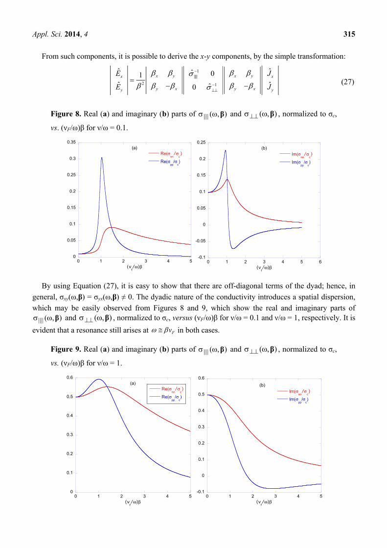
Figure 8. Real (a) and imaginary (b) parts of ),(|||| β and ),( β , normalized to σc,
vs. (νF/ω)β for ν/ω = 0.1.
By using Equation (27), it is easy to show that there are off-diagonal terms of the dyad; hence, in
general, σxy(ω,β) = σyx(ω,β) ≠ 0. The dyadic nature of the conductivity introduces a spatial dispersion,
which may be easily observed from Figures 8 and 9, which show the real and imaginary parts of ),(|||| β and ),( β , normalized to σc, versus (νF/ω)β for ν/ω = 0.1 and ν/ω = 1, respectively. It is
evident that a resonance still arises at vF in both cases.
Figure 9. Real (a) and imaginary (b) parts of ),(|||| β and ),( β , normalized to σc,
vs. (νF/ω)β for ν/ω = 1.
(b)

Appl. Sci. 2014, 4 316
The relation between the dyadic nature of the conductivity and the spatial dispersion is consistent
with the result obtained in [25], where the graphene conductivity dyad is derived from the Kubo
formula and numerically evaluated with an integral formulation.
5. Conclusions
In the operating conditions predicted for future electronic nano-interconnects, the low bias and the
low frequency allows the modeling of the electrical transport with a linearized semi-classical
electrodynamical model, which does not include interband transitions. This leads to a generalized
non-local dispersive Ohm’s law, which is regarded as the constitutive equation for the material. In the
2D case (graphene layer), the conductivity is dyadic and shows a spatial dispersion as an effect of the
coupling between the components. This coupling is absent in the long-wavelength limit. In the 1D case
(graphene nanoribbon), the transverse components of the currents are negligible, and the conductivity
reduces to a scalar quantity, modulated by the size and chirality, which strongly affect the number of
conducting channels.
Acknowledgments
This work has been supported by the EU grant # FP7-247007, under the project CACOMEL,
“Nano-CArbon based COmponents and Materials for high frequency ELectronics”.
Conflicts of Interest
The authors declare no conflict of interest.
References
1. Van Noorden, R. Moving towards a graphene world. Nature 2006, 442, 228–229.
2. Avouris, P.; Chen, Z.; Perebeinos, V. Carbon-based electronics. Nat. Nanotechnol. 2007, 2, 605–615.
3. Li, H.; Xu, C.; Srivastava, N.; Banerjee, K. Carbon nanomaterials for next-generation
interconnects and passives: Physics, status, and prospects. IEEE Trans. Electron Devices 2009,
56, 1799–1821.
4. International Technology Roadmap for Semiconductors, Edition 2013. Available online:
http://public.itrs.net (accessed on 23 May 2014).
5. Close, G.F.; Yasuda, S.; Paul, B.; Fujita, S.; Wong, H.-S.P. 1 GHz integrated circuit with carbon
nanotube interconnects and silicon transistors. Nano Lett. 2009, 8, 706–709.
6. Chen, X.; Akinwande, D.; Lee, K.-J.; Close, G.F.; Yasuda, S.; Paul, B.C.; Fujita, S.; Kong, J.;
Wong, H.-S.P. Fully integrated graphene and carbon nanotube interconnects for gigahertz
high-speed CMOS electronics. IEEE Trans. Electron Devices 2010, 57, 3137–3143.
7. Shulaker, M.M.; Hills, G.; Patil, N.; Wei, H.; Chen, H.-Y.; Wong, H.-S.P.; Mitra, S.
Carbon nanotube computer. Nature 2013, 501, 526–530.
8. Valitova, I.; Amato, M.; Mahvash, F.; Cantele, G.; Maffucci, A.; Santato, C.; Martel, R.;
Cicoira, F. Carbon nanotube electrodes in organic transistors. Nanoscale 2013, 5, 4638–4646.

Appl. Sci. 2014, 4 317
9. Burke, P.J. Luttinger liquid theory as a model of the gigahertz electrical properties of carbon
nanotubes. IEEE Trans. Nanotechnol. 2002, 1, 129–144.
10. Salahuddin, S.; Lundstrom, M.; Datta, S. Transport effects on signal propagation in quantum
wires. IEEE Trans. Electron Devices 2005, 52, 1734–1742.
11. Raychowdhury, A.; Roy, K. Modelling of metallic carbon-nanotube interconnects for circuit
simulations and a comparison with Cu interconnects for scaled technologies. IEEE Trans.
Comp.-Aided Des. Integr. Circuit Syst. 2006, 25, 58–65.
12. Maffucci, A.; Miano, G.; Villone, F. Performance comparison between metallic carbon nanotube
and copper nano-interconnects. IEEE Trans. Adv. Packag. 2008, 31, 692–699.
13. Xu, C.; Li, H.; Banerjee, K. Modeling, analysis, and design of graphene nano-ribbon interconnects.
IEEE Trans. Electron Devices 2009, 56, 1567–1578.
14. Naeemi, A.; Meindl, J.D. Compact physics-based circuit models for graphene nanoribbon
interconnects. IEEE Trans. Electron Devices 2009, 56, 1822–1833.
15. Cui, J.-P.; Zhao, W.-S.; Yin, W.-Y.; Hu, J. Signal transmission analysis of multilayer graphene
nano-ribbon (MLGNR) interconnects. IEEE Trans. Electromagn. Compat. 2012, 54, 126–132.
16. Maffucci, A.; Miano, G.; Villone, F. A transmission line model for metallic carbon nanotube
interconnects. Int. J. Circuit Theory Appl. 2008, 36, 31–51.
17. Maffucci, A.; Miano, G.; Villone, F. A new circuit model for carbon nanotube interconnects with
diameter-dependent parameters. IEEE Trans. Nanotechnol. 2009, 8, 345–354.
18. Miano, G.; Forestiere, C.; Maffucci, A.; Maksimenko, S.A.; Slepyan, G.Y. Signal propagation in
single wall carbon nanotubes of arbitrary chirality. IEEE Trans. Nanotechnol. 2011, 10, 135–149.
19. Forestiere, C.; Maffucci, A.; Maksimenko, S.A.; Miano, G.; Slepyan, G.Y. Transmission Line
model for multiwall carbon nanotubes with intershell tunneling. IEEE Trans. Nanotechnol. 2012,
11, 554–564.
20. Maffucci, A.; Miano, G. Transmission line model of graphene nanoribbon interconnects.
Nanosci. Nanotechnol. Lett. 2013, 5, 1207–1216.
21. Forestiere, C.; Maffucci, A.; Miano, G. Hydrodynamic model for the signal propagation along
carbon nanotubes. J. Nanophotonics 2010, 4, 041695.
22. Zheng, H.; Wang, Z.F.; Luo, T.; Shi, Q.W.; Chen, J. Analytical study of electronic structure in
armchair graphene nanoribbons. Phys. Rev. B 2007, 75, 165414.
23. Wakabayashi, K.; Sasaki, K.; Nakanishi, T.; Enoki, T. Electronic states of graphene nanoribbons
and analytical solutions. Sci. Technol. Adv. Mater. 2010, 11, 054504.
24. Chiariello, A.G.; Maffucci, A.; Miano, G. Circuit models of carbon-based interconnects for
nanopackaging. IEEE Trans. Compon. Packag. Manuf. Technol. 2013, 3, 1926–1937.
25. Araneo, R.; Lovat, G.; Burghignoli, P. Graphene nanostrip lines: Dispersion and attenuation. In
Proceedings of 16th IEEE Workshop on Signal and Power Integrity, Sorrento, Italy, 13–16 May
2012; pp. 75–78.
© 2014 by the authors; licensee MDPI, Basel, Switzerland. This article is an open access article
distributed under the terms and conditions of the Creative Commons Attribution license
(http://creativecommons.org/licenses/by/3.0/).
Top Related