


Languages
Pages
Legal

Research ArticleEffects of Deposition Time on the Morphology,Structure, and Optical Properties of PbS Thin FilmsPrepared by Chemical Bath Deposition
B. Abdallah ,1 A. Ismail,2 H. Kashoua,1 and W. Zetoun1
1Department of Physics, Atomic Energy Commission of Syria, P.O. Box 6091, Damascus, Syria2Department of Protection and Safety, Atomic Energy Commission of Syria, P.O. Box 6091, Damascus, Syria
Correspondence should be addressed to B. Abdallah; [email protected]
Received 27 November 2017; Revised 1 February 2018; Accepted 16 April 2018; Published 24 May 2018
Academic Editor: Victor M. Castaño
Copyright © 2018 B. Abdallah et al. This is an open access article distributed under the Creative Commons Attribution License,which permits unrestricted use, distribution, and reproduction in any medium, provided the original work is properly cited.
Lead sulfide thin films were prepared by chemical bath deposition (CBD) on both glass and Si (100) substrates. XRD analysis of thePbS film deposited at 25°C showed that the prepared films have a polycrystalline structure with (200) preferential orientation.Larger grains could be obtained by increasing the deposition time. The prepared films were also chemically characterized usingX-ray photoelectron spectroscopy (XPS), which confirmed the presence of lead and sulfur as PbS. While energy dispersive X-rayspectroscopy (EDX) technique was used to verify the stoichiometry of the prepared films. Atomic force microscopy (AFM) wasused to study the change in the films’ morphology with the deposition time. The effect of the deposition time, on both opticaltransmittance in the UV-Vis-NIR region and the structure of the film, was studied. The obtained results demonstrated that theoptical band gap decreased when the thickness increased.
1. Introduction
Lead sulfide (PbS) has attracted great interest due to itsenormous applications in the field of optoelectronics suchas infrared (IR) detection [1], solar cell [2], quantum dotsapplications [3], and selective coating for photothermalconversion [4]. PbS is a semiconductor with direct narrowenergy gap of 0.37–0.4 eV at room temperature. However,this energy gap becomes higher (1.6–2.44 eV) for nanocrys-talline materials because the sizes of the crystallite becomecomparable to the Bohr excitonic radius, so this differencecould be attributed to quantum confinement effect of PbSnanocrystals [5].
Also, among all other semiconductors, lead sulfide has apositive temperature coefficient of the energy gap [6]. PbSthin films could be prepared using different methods [7–9]such as pulsed laser ablation [10], spray pyrolysis [11], andchemical bath deposition (CBD) [12, 13]. However, chemicalbath deposition is mostly used [8, 14–17] since it is a suitable
method for the deposition of polycrystalline films, at low costand good-quality films [18]. In addition, chemical bath depo-sition does not require high-quality target and could beachieved without vacuum. The deposition rate and the thick-ness of the films are easily controlled by changing the spraydeposition parameters.
In a recent work [19, 20], the effect of ZnS film thicknesson its structural and electrical properties has been studied. Itwas demonstrated that by increasing the deposition time(thickness), the crystalline quality could be improved withdeveloping better conducting behavior.
Due to its simplicity and versatility, the chemical bathdeposition technique was used in this work to deposit PbSthin films on Si and glass substrates. EDX method wasemployed to reveal information about the composition ofthe films. The obtained films were then characterized byX-ray photoelectron spectroscopy (XPS) to analyze its chem-ical composition. XRD technique was used to study thecrystallographic properties of the prepared films. The
HindawiJournal of NanomaterialsVolume 2018, Article ID 1826959, 8 pageshttps://doi.org/10.1155/2018/1826959
crystalline quality was improved, where the grain size valuesincreased with increasing thickness. Also, the effect of thedeposition time on the physical properties of the PbS thinfilms was evaluated.
2. Experiment
Thin polycrystalline films of PbS were prepared by CBD onboth commercial glass slides and Si substrates. The substrateswere washed with hot distilled water, immersed in HCl solu-tion for 24h, and then washed with acetone. Finally, the sub-strates were cleaned ultrasonically with water for 20min.Lead acetate (Pb(CH3COO)2) and thiourea (SC(NH2)2) wereused as sources of Pb2+ and S2− ions to form nanocrystallinePbS thin films. Ammonium acetate NH4CH3CO2 was used asa buffer solution to control the nucleation rate [21]. Theaqueous solution of the deposition bath was prepared bythe sequential addition of 5ml of 0.5M lead acetate, 5mlof 2.0M KOH, 6ml of 1.0M thiourea, and 2ml of 1.0 Mtriethanolamine in a 100ml beaker. The total volume wascompleted to 100ml with distilled water. The deposition timehas been varied in the range of 10 to 120min. The quality ofthe films depends crucially on the deposition parameters,which should therefore be optimized in order to obtainhighly oriented crystalline PbS films.
A scanning electron microscope (SEM) TSCANVega\\XMU (Czech Republic), operated at 30 kV, was usedto measure the deposition time and the morphology of theprepared PbS films.
Atomic composition and stoichiometry of the PbS filmswere determined by EDX. The chemical composition of thefilms has been determined using the X-ray photoelectrontechnique. The XPS analyses were performed using a SPECSUHV/XPS/AES system with a hemispherical energy analyzer.The monochromated Al Kα X-ray source (1486.6 eV) is usedas the excitation source and is operated at 250W [22]. Inaddition, X-ray diffraction (XRD) STOE transmission X-ray diffractometer (Stadi P) (Germany) was used to analyzethe crystallographic properties of the prepared films, andlow-energy electrons issued from a flood gun were used tocompensate for the charging effect. The XRD analysis wasrealized by using the Cu Kα (λ = 0 15405 nm) radiation ina linear position sensitive detector for θ–2θ scan configura-tion. The morphology of the prepared PbS films was alsoanalyzed using AFM (Park Scientific Instruments AP-0100model) with the noncontact mode. The mean grain size,grain distribution, and surface roughness were determinedusing the WSxm software. In addition, the optical character-istics were examined by measuring the transmittance of theprepared films using a UV-Vis Shimadzu UV-310PC spec-trophotometer. The experimental set-up consists of UVexcitation using a 325nm He/Cd laser and grating mono-chromator (1200 groves/mm) equipped with a cooledphotomultiplier tube PMT. Two types of substrates wereused for different methods of analysis. EDX analysis is betterperformed for films on silicon substrate, while a UV trans-mission study requires films deposited on transparent mate-rials in the visible region such as glass substrate.
3. Results and Discussion
3.1. Composition Study
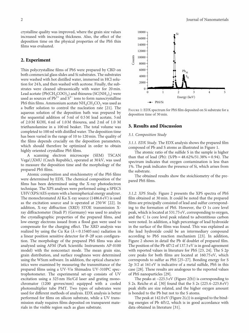
3.1.1. EDX Study. The EDX analysis shows the prepared filmcomposed of Pb and S atoms as illustrated in Figure 1.
The atomic ratio of the sulfide S in the sample is higherthan that of lead (Pb): (S/Pb = 48 62%/51 38% = 0 94). Thespectrum indicates that oxygen contamination is less than1%. The peak indicates the presence of Si, which arises fromthe substrate.
The obtained results show the stoichiometry of the pre-pared PbS films.
3.1.2. XPS Study. Figure 2 presents the XPS spectra of PbSfilm obtained at 30min. It could be noted that the preparedfilms are principally consisted of lead and sulfur correspond-ing to the formation of PbS. However, the O 1s core levelpeak, which is located at 531.75 eV, corresponding to oxygen,and the C 1s core level peak related to adventitious carbonwere noted. In addition, a high percentage of lead hydroxidein the surface of the films was found. This was explained asthe lead hydroxide could be an intermediary compoundaccording to PbS reaction mechanism [23]. In addition,Figure 2 shows in detail the Pb 4f doublet of prepared film.The position of the Pb 4f7/2 of 137.5 eV is in good agreementwith reported values in literature for PbS [23, 24]. The S 2pcore peaks for both films are located at 160.75 eV, whichcorresponds to sulfur as PbS [25–27]. Bonding energy for S2p 3/2 at 161 eV is indicative of a metal sulfide, PbS in thiscase [28]. These results are analogous to the reported valuesof PbS nanoparticles [29].
The peaks at ~225.5 eV (Figure 2(b)) is corresponding toS 2s. Reiche et al. [30] found that the S 2s (225.4–225.8 eV)peak shifts are size related, and the higher oxygen amountis bonded to the Pb but not to the S atoms.
The peak at 142.0 eV (Figure 2(c)) is assigned to the bind-ing energies of Pb 4f5/2, which is in good accordance withdata obtained in literature [31].
1Energy (keV)2 3 4 50
Cou
nts
PbS/Si
18000
16000
14000
12000
10000
8000
6000
4000
2000
0
Si
PbMSK
Figure 1: EDX spectrum for PbS film deposited on Si substrate for adeposition time of 30min.
2 Journal of Nanomaterials

3.2. XRD Study. Figure 3 shows XRD pattern of PbS filmsdeposited for different times, and all reflected peaks with(200) preferential orientation can be indexed to the cubicstructure of PbS with lattice parameters a = 0 59143 nm,and it shows that small peaks (111), (220) (311), and (222)correspond to 26.10°, 43.22°, 51.20°, and 53.62°, respectively,in good agreement with the PDF database (number 78-1054). The two small peaks at 34.1° and 47.5° are due to thestainless steel 304 holder. It has been observed that the inten-sity of the peaks increased and the crystallization of PbS thinfilms were improved with increasing film thickness, similarto other reports [12].
The intensity of the XRD (200) peak gets strongerwith deposition time indicating the increase of the filmthickness as shown in Figure 3(a). Grain size has beendeduced from XRD pattern using Scherrer’s formula [32]for (111), (200) (220), and (311) orientations. It was foundthat the crystallite size increases with increasing the thick-ness (Figure 3(b)).
The grain size for the (111) peak increased from 10nm to27nm with increasing thickness, whereas the grain size forthe (200) peak increased from 26nm to 47nm. This behavioris in agreement with other studies [11]. This means that thethicker films have less defect concentrations (bigger grainsize and fine grain boundary). The behavior of increasingthe resistivity with average grain size agrees with otherreported work [33] but does not agree with other studies ofZnS film deposited by ultrasonic spray pyrolysis [19, 20].The increase in the film thickness leads to an improvementof the crystalline quality. This is attributed to the strain inthe film introduced during the deposition [34], that is, thethicker films suffer less strain than the thinner ones. Thiscomes in a good agreement with our results where thickerfilms have lower stress value and better quality.
3.3. SEM and AFM Study. This kind of texture and growthwas found in all samples under investigation and con-firmed the analysis already presented. The morphology of
Pb4p3/2
O
S2p
C
Pb5d
Pb4f7/2
Pb4f5/2
Pb4d3/2
Pb4d5/2
0
5000
10000
15000
20000
25000
30000
Inte
nsity
(a.u
)
700 600 500 400 300 200 100 0800Binding energy (eV)
(a)
S2S
10800
11000
1120011400
11600
11800
12000
12200
124001260012800
Inte
nsity
(a.u
)
235 230 225 220 215 210240Binding energy (eV)
S 2s
(b)
Pb4f5/2
Pb4f7/2
S2p
0
5000
10000
15000
20000
25000
30000
35000
Inte
nsity
(a.u
)
170 160 150 140 130 120 110180Binding energy (eV)
Pb 4f
(c)
Figure 2: (a) XPS survey scan for PbS deposited at 30min and (b and c) XPS high-resolution spectra for sample prepared S 2s and for Pb,respectively.
3Journal of Nanomaterials

the films deposited at a certain time depends mainly onthe deposition rate, pH, concentration, and speed of thesubstrate rotation [35].
The cross-section of PbS thin film deposited for 100minis shown in Figure 4(a) where the thickness was about320nm. The surface morphology is shown in Figure 4(b).
The AFM surface topography of as-deposited PbS film attime 10min (Figures 5(a) and 5(b)) shows a nanostructuredsurface with well-defined grains of mean size = 13 nm. The
surfaces of the products of PbS thin films were obviouslysmooth. The AFM surface topography (Figures 5(c) and5(d)) changes for thicker film deposited at 100min (corre-sponding thickness: 320 nm).
The roughness of the prepared films, expressed as rootmean square (RMS) roughness was obtained from AFMmeasurements, and their evolutions with deposition timeare increased by increasing the thickness, where it variedfrom 2nm (at 70 nm thickness) to a maximum value of
20 min30 min40 min50 min60 min
80 min
100 min
120 min(222)
(311)(220)
SS
(200)
(111)
10 min0
500
1000
1500
2000
2500
3000
3500
4000
Inte
nsity
(a.u
.)
20 25 30 35 40 45 50 55 60152�휃 (degrees)
(a)
15
20
25
30
35
40
45
50
Gra
in si
ze (n
m)
100 150 200 250 300 350 40050�ickness (nm)
(111)(200)
(220)(311)
(b)
Figure 3: (a) XRD pattern of PbS thin film and (b) grain size evolution with film thickness deposited on glass substrate for different times.
SEM MAG: 50.00 kxScan speed: 7SEM HV: 20.00 KV Arab European University
Det: SE VEGA\\ TESCANSM: RESOLUTION 500 nm
(a)
Arab European University
VEGA\\ TESCANSEM MAG: 3.00 kxScan speed: 7SEM HV: 10.00 KV
Det: SESM: RESOLUTION 500 �휇m
(b)
Figure 4: Typical SEM micrographs of PbS/Si thin films deposited for 100min: (a) cross-sectional view and (b) surface view.
4 Journal of Nanomaterials
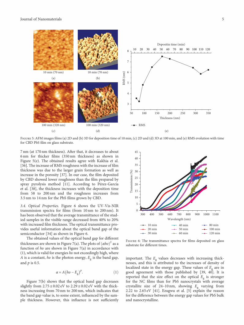
7nm (at 170nm thickness). After that, it decreases to about6 nm for thicker films (350 nm thickness) as shown inFigure 5(e). The obtained results agree with Kakhia et al.[36]. The increase of RMS roughness with the increase of filmthickness was due to the larger grain formation as well asincrease in the porosity [37]. In our case, the film depositedby CBD showed lower roughness than the film prepared byspray pyrolysis method [11]. According to Pérez-Garcíaet al. [38], the thickness increases with the deposition timefrom 58 to 200nm and the roughness increases from3.5 nm to 14nm for the PbS films grown by CBD.
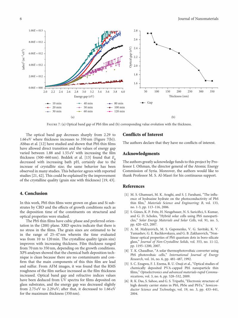
3.4. Optical Properties. Figure 6 shows the UV-Vis-NIRtransmission spectra for films (from 10nm to 200nm). Ithas been observed that the average transmittance of the stud-ied samples in the visible range decreased from 40% to 20%with increased film thickness. The optical transmittance pro-vides useful information about the optical band gap of thesemiconductor [34] as shown in Figure 6.
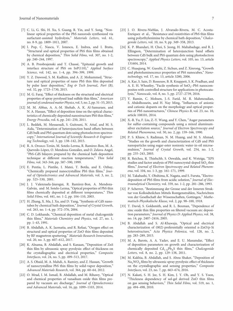
The obtained values of the optical band gap for differentthicknesses are shown in Figure 7(a). The plots of αhυ 2 as afunction of hυ are shown in Figure 7(a) in accordance with(1), which is valid for energies hυ not exceedingly high, whereA is a constant, hυ is the photon energy, Eg is the band gap,and p is 0.5.
α = A hυ − Egp 1
Figure 7(b) shows that the optical band gap decreasesslightly from 2.75± 0.02 eV to 2.29± 0.02 eV with the thick-ness increasing from 70nm to 200 nm, which indicates thatthe band gap value is, to some extent, influenced by the sam-ple thickness. However, this influence is not sufficiently
important. The Eg values decreases with increasing thick-nesses, and this is attributed to the increases of density oflocalized state in the energy gap. These values of Eg are ingood agreement with those published by [39, 40]. It isreported that the size effect on the optical Eg is strongerfor the NC films than for PbS nanocrystals with averagecrystallite size of 24–10nm, showing Eg varying from2.22 to 2.65 eV [41]. Ezugwu et al. [5] explain the reasonfor the difference between the energy gap values for PbS bulkand nanocrystalline.
10 min (70 nm)
(a)
10 min (70 nm)
(b)
100 min (320 nm)
(c)
100 min (320 nm)
(d)
100 150 200 250 300 35050Thickness (nm)
3
4
5
6
7
8
RMS
(nm
)
10 20 30 40 50 60 70 80 90 100 110 120Depositin time (min)
RMS
(e)
Figure 5: AFM images films (a) 2D and (b) 3D for deposition time of 10min, (c) 2D and (d) 3D at 100min, and (e) RMS evolution with timefor CBD PbS film on glass substrate.
0
5
10
15
20
25
30
35
40
45
Tran
smiss
ion
(%)
400 500 600 700 800 900 1000 1100300Wavelength (nm)
50 min10 min
60 min20 min
40 min
30 min
80 min100 min120 min
Figure 6: The transmittance spectra for films deposited on glasssubstrate for different times.
5Journal of Nanomaterials
The optical band gap decreases sharply from 2.29 to1.66 eV where thickness increases to 350nm (Figure 7(b)).Abbas et al. [12] have studied and shown that PbS thin filmshave allowed direct transition and the values of energy gapvaried between 1.88 and 1.55 eV with increasing the filmthickness (500–660nm). Beddek et al. [13] found that Egdecreased with increasing bath pH, certainly due to theincrease of crystallite size; the same behavior has beenobserved in many studies. This behavior agrees with reportedstudies [21, 42]. This could be explained by the improvementof the crystalline quality (grain size with thickness) [19, 43].
4. Conclusion
In this work, PbS thin films were grown on glass and Si sub-strates by CBD and the effects of growth conditions such asthe deposition time of the constituents on structural andoptical properties were studied.
The PbS thin films have cubic phase and preferred orien-tation in the (200) plane. XRD spectra indicate that there isno stress in the films. The grain sizes are estimated to bein the range of 25–47 nm wherein the time evaluatedwas from 10 to 120min. The crystalline quality (grain size)improves with increasing thickness. Film thickness rangedfrom 70nm to 350nm, depending on the growth conditions.XPS analyses showed that the chemical bath deposition tech-nique is clean because there are no contaminants and con-firm that the main components of this thin film are leadand sulfur. From AFM images, it was found that the RMSroughness of the film surface increased as the film thicknessincreased. Optical band gap and refractive indices valueshave been deduced from UV spectra for films deposited onglass substrates, and the energy gap was decreased slightlyfrom 2.75 eV to 2.29 eV; after that, it decreased to 1.66 eVfor the maximum thickness (350 nm).
Conflicts of Interest
The authors declare that they have no conflicts of interest.
Acknowledgments
The authors greatly acknowledge funds to this project by Pro-fessor I. Othman, the director general of the Atomic EnergyCommission of Syria. Moreover, the authors would like tothank Professor M. S. Al-Masri for his continuous support.
References
[1] M. S. Ghamsari, M. K. Araghi, and S. J. Farahani, “The influ-ence of hydrazine hydrate on the photoconductivity of PbSthin film,” Materials Science and Engineering: B, vol. 133,no. 1-3, pp. 113–116, 2006.
[2] S. Günes, K. P. Fritz, H. Neugebauer, N. S. Sariciftci, S. Kumar,and G. D. Scholes, “Hybrid solar cells using PbS nanoparti-cles,” Solar Energy Materials and Solar Cells, vol. 91, no. 5,pp. 420–423, 2007.
[3] A. M. Malyarevich, M. S. Gaponenko, V. G. Savitski, K. V.Yumashev, G. E. Rachkovskaya, and G. B. Zakharevich, “Non-linear optical properties of PbS quantum dots in boro-silicateglass,” Journal of Non-Crystalline Solids, vol. 353, no. 11-12,pp. 1195–1200, 2007.
[4] T. K. Chaudhur, “A solar thermophotovoltaic converter usingPbS photovoltaic cells,” International Journal of EnergyResearch, vol. 16, no. 6, pp. 481–487, 1992.
[5] S. C. Ezugwu, F. I. Ezema, R. U. Osuji et al., “Optical studies ofchemically deposited PVA-capped PbS nanoparticle thinfilms,” Optoelectronics and advanced materials-rapid Commu-nications, vol. 3, no. 6, pp. 528–532, 2009.
[6] R. K. Das, S. Sahoo, and G. S. Tripathi, “Electronic structure ofhigh density carrier states in PbS, PbSe and PbTe,” Semicon-ductor Science and Technology, vol. 19, no. 3, pp. 433–441,2004.
2.2 2.4 2.6 2.8 3.0 3.2 3.4 3.6 3.8 4.02.0Energy gap (eV)
0.00E + 000
2.00E + 012
4.00E + 012
6.00E + 012
8.00E + 012
1.00E + 013
(�훼hυ
)2 (m−2
·eV2 )
10 min20 min30 min
40 min50 min60 min
80 min100 min120 min
(a)
1.6
1.8
2.0
2.2
2.4
2.6
2.8
Opt
ical
gap
(eV
)
100 150 200 250 300 35050Thickness (nm)
Gap
(b)
Figure 7: (a) Optical band gap of PbS film and (b) corresponding value evolution with the thickness.
6 Journal of Nanomaterials
[7] C. Li, G. Shi, H. Xu, S. Guang, R. Yin, and Y. Song, “Non-linear optical properties of the PbS nanorods synthesized viasurfactant-assisted hydrolysis,” Materials Letters, vol. 61,no. 8-9, pp. 1809–1811, 2007.
[8] I. Pop, C. Nascu, V. Ionescu, E. Indrea, and I. Bratu,“Structural and optical properties of PbS thin films obtainedby chemical deposition,” Thin Solid Films, vol. 307, no. 1-2,pp. 240–244, 1997.
[9] A. B. Preobrajenski and T. Chassé, “Epitaxial growth andinterface structure of PbS on InP(110),” Applied SurfaceScience, vol. 142, no. 1–4, pp. 394–399, 1999.
[10] Y. Z. Dawood, S. M. Kadhim, and A. Z. Mohammed, “Struc-ture and optical properties of nano PbS thin film depositedby pulse laser deposition,” Eng & Tech Journal,. Part (B),vol. 32, pp. 1723–1730, 2015.
[11] M. G. Faraj, “Effect of thickness on the structural and electricalproperties of spray pyrolysed lead sulfide thin films,” Americanjournal of condensedmatter Physics, vol. 5, no. 2, pp. 51–55, 2015.
[12] M. M. Abbas, A. A.-M. Shehab, A. K. Al-Samuraee, andN. A. Hassan, “Effect of deposition time on the optical charac-teristics of chemically deposited nanostructure PbS thin films,”Energy Procedia, vol. 6, pp. 241–250, 2011.
[13] L. Beddek, M. Messaoudi, S. Guitouni, N. Attaf, and M. S.Aida, “Determination of heterojunction band offsets betweenCdS bulk and PbS quantum dots using photoelectron spectros-copy,” International Journal of Scientific Research & Engineer-ing Technology, vol. 3, pp. 138–142, 2015.
[14] R. A. Orozco-Terán, M. Sotelo-Lerma, R. Ramirez-Bon, M. A.Quevedo-López, O. Mendoza-González, and O. Zelava-Angel,“PbS-CdS bilayers prepared by the chemical bath depositiontechnique at different reaction temperatures,” Thin SolidFilms, vol. 343-344, pp. 587–590, 1999.
[15] E. Pentia, L. Pintilie, I. Matei, T. Botila, and E. Ozbay,“Chemically prepared nanocrystalline PbS thin films,” Jour-nal of Optoelectronics and Advanced Materials, vol. 3, no. 2,pp. 525–530, 2001.
[16] J. J. Valenzuela-Jáuregui, R. Ramırez-Bon, A. Mendoza-Galván, and M. Sotelo-Lerma, “Optical properties of PbS thinfilms chemically deposited at different temperatures,” ThinSolid Films, vol. 441, no. 1-2, pp. 104–110, 2003.
[17] H. Zhang, X. Ma, J. Xu, and D. Yang, “Synthesis of CdS nano-tubes by chemical bath deposition,” Journal of Crystal Growth,vol. 263, no. 1–4, pp. 372–376, 2004.
[18] C. D. Lokhande, “Chemical deposition of metal chalcogenidethin films,” Materials Chemistry and Physics, vol. 27, no. 1,pp. 1–43, 1991.
[19] B. Abdallah, A. K. Jazmatia, and R. Refaai, “Oxygen effect onstructural and optical properties of ZnO thin films depositedby RF magnetron sputtering,”Materials Research Innovations,vol. 20, no. 3, pp. 607–612, 2017.
[20] K. Alnama, B. Abdallah, and S. Kanaan, “Deposition of ZnSthin film by ultrasonic spray pyrolysis: effect of thickness onthe crystallographic and electrical properties,” CompositeInterfaces, vol. 24, no. 5, pp. 499–513, 2017.
[21] A. S. Obaid, M. A. Mahdi, A. Ramizy, and Z. Hassan, “Growthof nanocrystalline PbS thin films by solid-vapor deposition,”Advanced Materials Research, vol. 364, pp. 60–64, 2012.
[22] O. Mrad, I. M. Ismail, B. Abdallah, and M. Rihawy, “Opticaland chemical properties of vanadium oxide thin films pre-pared by vacuum arc discharge,” Journal of Optoelectronicsand Advanced Materials, vol. 16, pp. 1099–1103, 2014.
[23] J. O. Rivera-Nieblas, J. Alvarado-Rivera, M. C. Acosta-Enríquez et al., “Resistance and resistivities of PbS thin filmsusing polyethylenimine by chemical bath deposition,” Chalco-genide Letters, vol. 10, no. 9, pp. 349–358, 2013.
[24] K. P. Bhandari, H. Choi, S. Jeong, H. Mahabaduge, and R. J.Ellingson, “Determination of heterojunction band offsetsbetween CdS bulk and PbS quantum dots using photoelectronspectroscopy,” Applied Physics Letters, vol. 105, no. 13, article131604, 2014.
[25] C. Huaqiang, W. Guozhi, Z. Sichun, and Z. Xinrong, “Growthand photoluminescence properties of PbS nanocubes,” Nano-technology, vol. 17, no. 13, article 3280, 2006.
[26] A. Kar, S. Sain, D. Rossouw, B. R. Knappett, S. K. Pradhan, andA. E. H. Wheatley, “Facile synthesis of SnO2–PbS nanocom-posites with controlled structure for applications in photocata-lysis,” Nanoscale, vol. 8, no. 5, pp. 2727–2739, 2016.
[27] Y. Ramin, C. Mohsen, J.-S. Farid, M. R. Mahmoudian,S. Abdolhossein, and H. Nay Ming, “Influences of anionicand cationic dopants on the morphology and optical proper-ties of PbS nanostructures,” Chinese Physics B, vol. 23, no. 10,article 108101, 2014.
[28] X.-R. Yu, F. Liu, Z.-Y. Wang, and Y. Chen, “Auger parametersfor sulfur-containing compounds using a mixed aluminum-silver excitation source,” Journal of Electron Spectroscopy andRelated Phenomena, vol. 50, no. 2, pp. 159–166, 1990.
[29] P. S. Khiew, S. Radiman, N. M. Huang, and M. S. Ahmad,“Studies on the growth and characterization of CdS and PbSnanoparticles using sugar-ester nonionic water-in-oil microe-mulsion,” Journal of Crystal Growth, vol. 254, no. 1-2,pp. 235–243, 2003.
[30] R. Reichea, R. Thielschb, S. Oswalda, and K. Wetziga, “XPSstudies and factor analysis of PbS nanocrystal-doped SiO2 thinfilms,” Journal of Electron Spectroscopy and Related Phenom-ena, vol. 104, no. 1-3, pp. 161–171, 1999.
[31] M. Takahashi, Y. Ohshima, K. Nagata, and S. Furuta, “Electro-deposition of PbS films from acidic solution,” Journal of Elec-troanalytical Chemistry, vol. 359, no. 1-2, pp. 281–286, 1993.
[32] P. Scherrer, “Bestimmung der Grosse und der Inneren Struk-tur von Kolloidteilchen Mittels Rontgenstrahlen, Nachrichtenvon der Gesellschaft der Wissenschaften, Gottingen,” Mathe-matisch-Physikalische Klasse, vol. 2, pp. 98–100, 1918.
[33] T. David, S. Goldsmith, and R. L. Boxman, “Dependence ofzinc oxide thin film properties on filtered vacuum arc deposi-tion parameters,” Journal of Physics D: Applied Physics, vol. 38,no. 14, pp. 2407–2416, 2005.
[34] B. Abdallah and S. Al-Khawaja, “Optical and electricalcharacterization of (002)-preferentially oriented n-ZnO/p-Siheterostructure,” Acta Physica Polonica, vol. 128, no. 2,pp. 283–289, 2015.
[35] M. A. Barote, A. A. Yadav, and E. U. Masumdar, “Effectof deposition parameters on growth and characterization ofchemically deposited Cd1-XPbXS thin films,” ChalcogenideLetters, vol. 8, no. 2, pp. 129–138, 2011.
[36] M. Kakhia, B. Abdallah, and S. Abou Shaker, “Deposition ofNa2WO4 films by ultrasonic spray pyrolysis: effect of thicknesson the crystallographic and sensing properties,” CompositeInterfaces, vol. 23, no. 7, pp. 663–674, 2016.
[37] N. Kakati, S. H. Jee, S. H. Kim, J. Y. Oh, and Y. S. Yoon,“Thickness dependency of sol-gel derived ZnO thin filmson gas sensing behaviors,” Thin Solid Films, vol. 519, no. 1,pp. 494–498, 2010.
7Journal of Nanomaterials

[38] C. E. Pérez-García, R. Ramírez-Bon, and Y. V. Vorobiev,“PbS thin films growth with CBD and PCBD techniques: acomparative study,” Chalcogenide Letters, vol. 12, no. 11,pp. 579–588, 2015.
[39] R. K. Joshi, A. Kanjilal, and H. Sehgal, “Solution grown PbSnanoparticle films,” Applied Surface Science, vol. 221, no. 1-4,pp. 43–47, 2004.
[40] A. U. Ubale, A. R. Junchara, N. H. Wadibhasme, A. S. D.Purkab, R. B. Mankar, and V. S. Sangawar, “Thicknessdependent structural, electrical and optical properties ofchemically deposited nanopartical PbS thin films,” TurkishJournal of Physics, vol. 31, pp. 279–286, 2007.
[41] Z. Bo, L. Guanghai, Z. Jun, Z. Yong, and Z. Lide, “Synthesisand characterization of PbS nanocrystals in water/C12E9/cyclohexane microemulsions,” Nanotechnology, vol. 14, no. 4,pp. 443–446, 2003.
[42] T. C. Chi, “Structure, morphology, and optical propertiesof the compact, vertically-aligned ZnO nanorod thin filmsby the solution-growth technique,” in Nanorods InTech, O.Yalçın, Ed., p. 33, InTech, Croatia, 2012.
[43] S. Al-Khawaja, B. Abdallah, S. Abou Shaker, and M. Kakhia,“Thickness effect on stress, structural, electrical and sensingproperties of (0 0 2) preferentially oriented undoped ZnO thinfilms,” Composite Interfaces, vol. 22, no. 3, pp. 221–231, 2015.
8 Journal of Nanomaterials

CorrosionInternational Journal of
Hindawiwww.hindawi.com Volume 2018
Advances in
Materials Science and EngineeringHindawiwww.hindawi.com Volume 2018
Hindawiwww.hindawi.com Volume 2018
Journal of
Chemistry
Analytical ChemistryInternational Journal of
Hindawiwww.hindawi.com Volume 2018
Scienti�caHindawiwww.hindawi.com Volume 2018
Polymer ScienceInternational Journal of
Hindawiwww.hindawi.com Volume 2018
Hindawiwww.hindawi.com Volume 2018
Advances in Condensed Matter Physics
Hindawiwww.hindawi.com Volume 2018
International Journal of
BiomaterialsHindawiwww.hindawi.com
Journal ofEngineeringVolume 2018
Applied ChemistryJournal of
Hindawiwww.hindawi.com Volume 2018
NanotechnologyHindawiwww.hindawi.com Volume 2018
Journal of
Hindawiwww.hindawi.com Volume 2018
High Energy PhysicsAdvances in
Hindawi Publishing Corporation http://www.hindawi.com Volume 2013Hindawiwww.hindawi.com
The Scientific World Journal
Volume 2018
TribologyAdvances in
Hindawiwww.hindawi.com Volume 2018
Hindawiwww.hindawi.com Volume 2018
ChemistryAdvances in
Hindawiwww.hindawi.com Volume 2018
Advances inPhysical Chemistry
Hindawiwww.hindawi.com Volume 2018
BioMed Research InternationalMaterials
Journal of
Hindawiwww.hindawi.com Volume 2018
Na
nom
ate
ria
ls
Hindawiwww.hindawi.com Volume 2018
Journal ofNanomaterials
Submit your manuscripts atwww.hindawi.com
Top Related