
![[A2DP] [AVRCP] - JVC...Motorola Atrix — Motorola Atrix 2 N/A N/A NG Motorola BACKFLIP ME600 —— ——NG Motorola DEFY MB525 — Motorola Droid 2 (Milestone 2) —— Motorola](https://static.fdocuments.net/doc/165x107/5fa61ea866868c7082174373/a2dp-avrcp-jvc-motorola-atrix-a-motorola-atrix-2-na-na-ng-motorola.jpg)


![chapter · 2006. 12. 8. · mo de instruction set of a commercial micropro cessor, the Motorola MC68020 [25, 5] and then used the formal mo del to v erify man y binary mac hine co](https://static.fdocuments.net/doc/165x107/6128dac9c13caa14b246f56e/chapter-2006-12-8-mo-de-instruction-set-of-a-commercial-micropro-cessor-the.jpg)
Languages
Pages
Legal


EE314
IBM/Motorola Power PC620
IBM Power PC 601
Motorola MC68020
Field EffectField Effect Transistors Transistors

Chapter 12: Field Effect Transistors
1.Construction of MOS2.NMOS and PMOS3.Types of MOS 4.MOSFET Basic
Operation5.Characteristics

The MOS Transistor
Polysilicon Aluminum
JFET – Junction Field Effect Transistor
MOSFET - Metal Oxide Semiconductor Field Effect Transistor
n-channel MOSFET (nMOS) & p-channel MOSFET (pMOS)
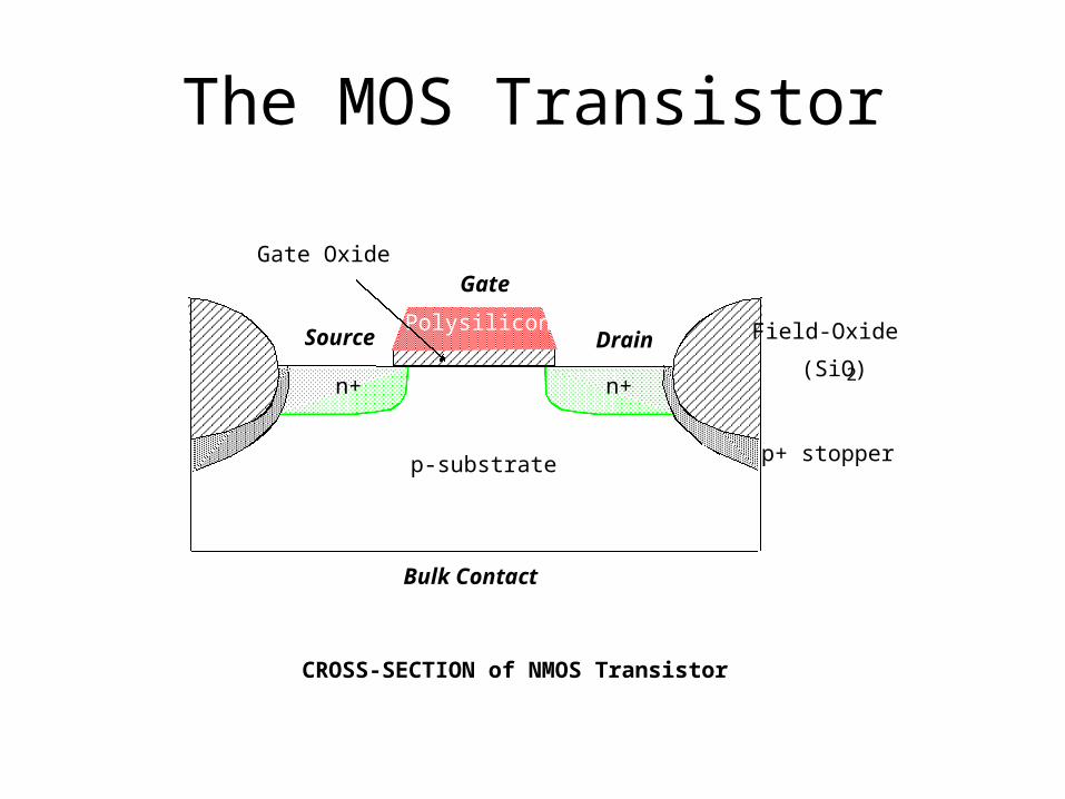
The MOS Transistor
n+n+
p-substrate
Field-Oxide
(SiO2)
p+ stopper
Polysilicon
Gate Oxide
DrainSource
Gate
Bulk Contact
CROSS-SECTION of NMOS Transistor
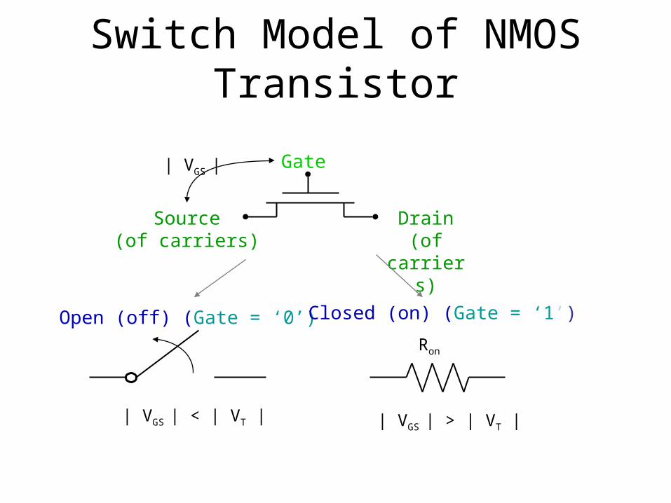
Switch Model of NMOS Transistor
Gate
Source(of carriers)
Drain(of
carriers)
| VGS |
| VGS | < | VT | | VGS | > | VT |
Open (off) (Gate = ‘0’) Closed (on) (Gate = ‘1’)
Ron

Switch Model of PMOS Transistor
Gate
Source(of carriers)
Drain(of carriers)
| VGS |
| VGS | > | VDD – | VT | | | VGS | < | VDD – |VT| |
Open (off) (Gate = ‘1’) Closed (on) (Gate = ‘0’)Ron

MOS transistors Symbols
D
S
G
D
S
G
G
S
D D
S
G
NMOS Enhancement NMOS
PMOS
Depletion
Enhancement
B
NMOS withBulk Contact
Channel
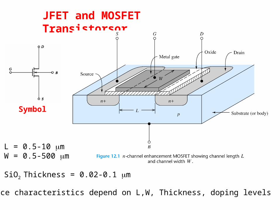
JFET and MOSFET Transistorsor
L = 0.5-10 mW = 0.5-500 m
SiO2 Thickness = 0.02-0.1 m
Device characteristics depend on L,W, Thickness, doping levels
Symbol

MOSFET Transistor Fabrication Steps
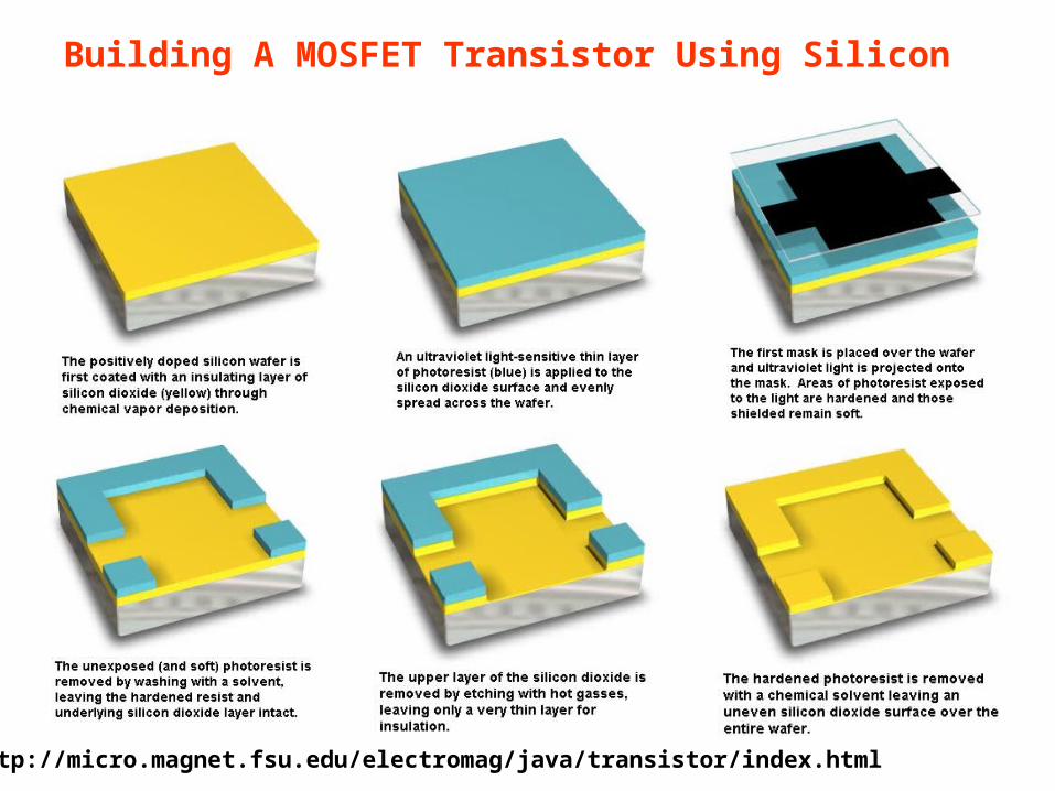
Building A MOSFET Transistor Using Silicon
http://micro.magnet.fsu.edu/electromag/java/transistor/index.html


It is done. Now, how does it work?

n-channel MOSFET Basic OperationOperation in the Cutoff region
Schematic
pn junction: reverse bias
iD=0
for vGS<Vt0
When vGS=0 then iD=0 until vGS>Vt0 (Vt0 –threshold voltage)

n-channel MOSFET Basic OperationOperation in the Triode Region
For vDS<vGS-Vt0 and vGS>Vt0 the NMOS is operating in the triode region
Resistor like characteristic(R between S & D, Used as voltage controlled R)
For small vDS, iD is proportional to the excess voltage vGS-Vt0

n-channel MOSFET Basic OperationOperation in the Triode Region
202 DSDStGSD vvVvKi
2
KP
L
WK
Device parameter KP for NMOSFET is 50 A/V2

n-channel MOSFET Basic OperationOperation in the Saturation Region (vDS is increased)
Tapering of the channel- increments of iD are smaller when vDS islarger When vGD=Vt0 then the
channel thickness is 0 and
20tGSD VvKi
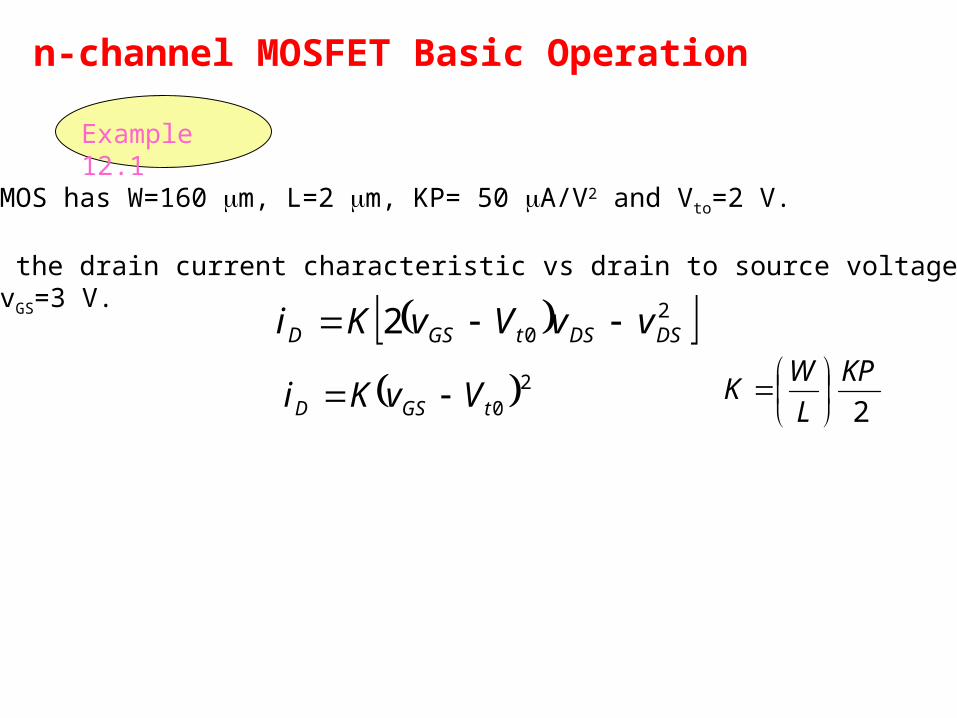
n-channel MOSFET Basic Operation
Example 12.1
An nMOS has W=160 m, L=2 m, KP= 50 A/V2 and Vto=2 V.
Plot the drain current characteristic vs drain to source voltage for vGS=3 V.
2
KP
L
WK
202 DSDStGSD vvVvKi
20tGSD VvKi
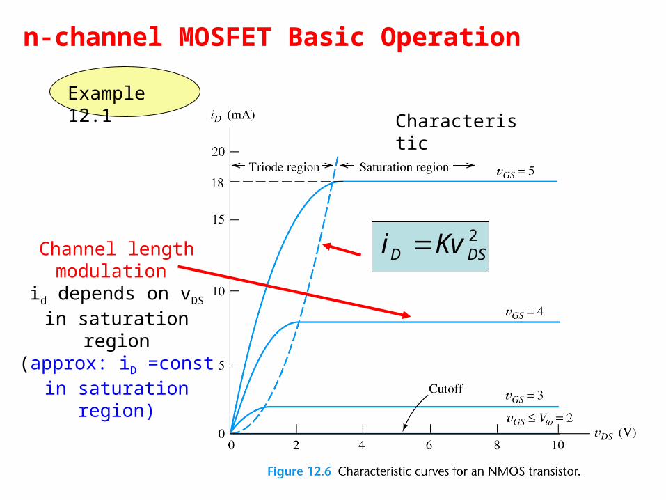
n-channel MOSFET Basic Operation
Characteristic
2DSD Kvi
Example 12.1
Channel lengthmodulation
id depends on vDS in saturation region
(approx: iD =const in saturation region)

p-channel MOSFET Basic OperationIt is constructed by interchanging the n and p regions of n-channel MOSFET.
SymbolCharacteristic
How does p-channel MOSFET operate?-voltage polarities-iD current-schematic
Top Related