


Languages
Pages
Legal


FloorplanningECE6133
Physical Design Automation of VLSI Systems
Prof. Sung Kyu LimSchool of Electrical and Computer Engineering
Georgia Institute of Technology
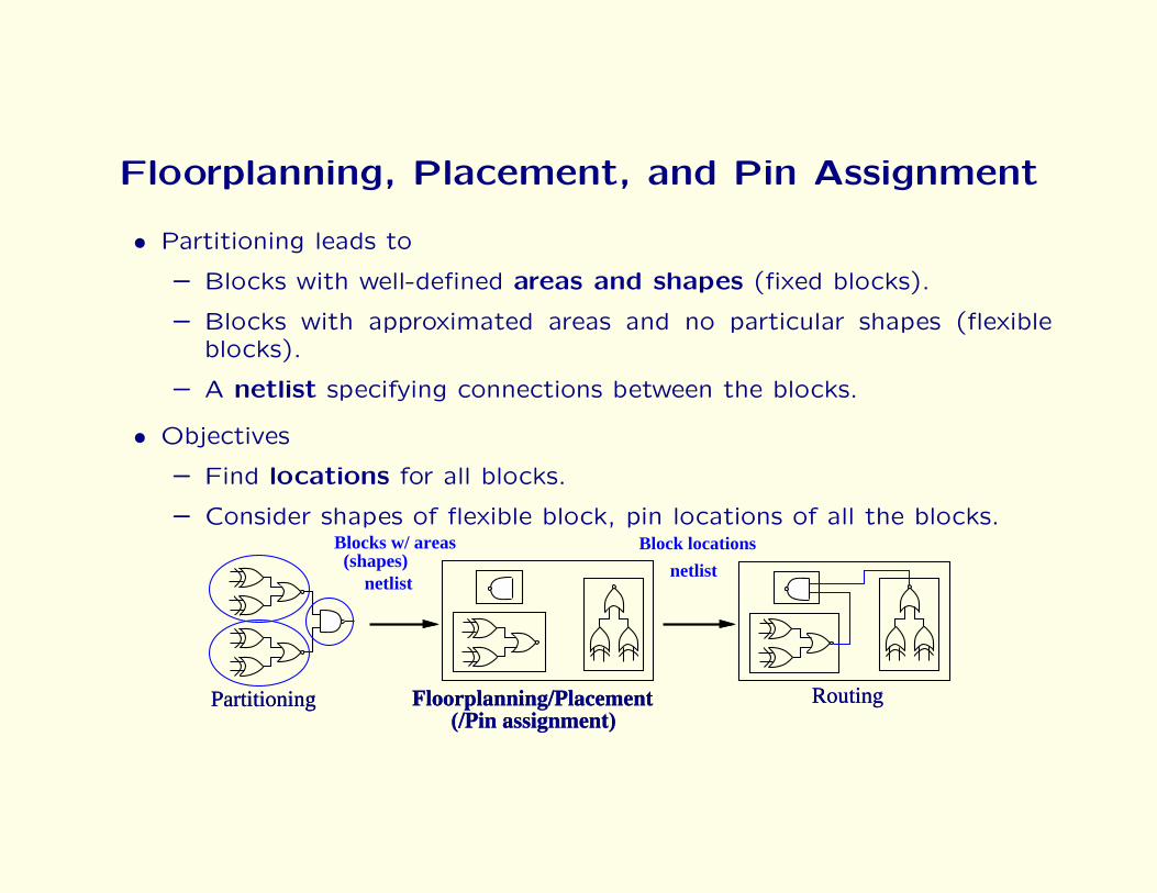
Floorplanning, Placement, and Pin Assignment
• Partitioning leads to
– Blocks with well-defined areas and shapes (fixed blocks).
– Blocks with approximated areas and no particular shapes (flexibleblocks).
– A netlist specifying connections between the blocks.
• Objectives
– Find locations for all blocks.
– Consider shapes of flexible block, pin locations of all the blocks.
Partitioning RoutingFloorplanning/Placement (/Pin assignment)
Blocks w/ areas (shapes)
netlist
Block locations
netlist
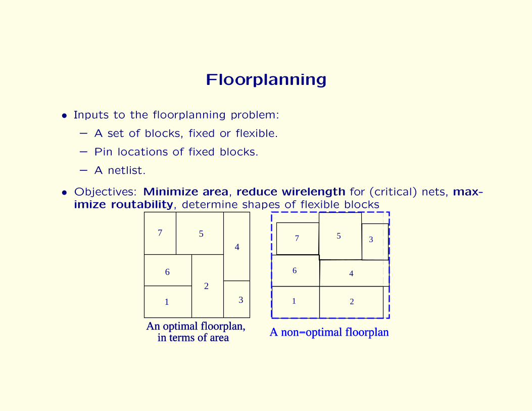
Floorplanning
• Inputs to the floorplanning problem:
– A set of blocks, fixed or flexible.
– Pin locations of fixed blocks.
– A netlist.
• Objectives: Minimize area, reduce wirelength for (critical) nets, max-imize routability, determine shapes of flexible blocks
7 5
4
2
1
6
3
A non−optimal floorplanAn optimal floorplan, in terms of area
1
6
7 5
2
4
3

Floorplan Design
x
y
Aspect ratio: r <= y/x <= s
Rotation:
Area: A=xy
Modules:
Module connectivity
3
2
5
3 6
52
1
a b
c d
e f
a
bc
d
e
f
g
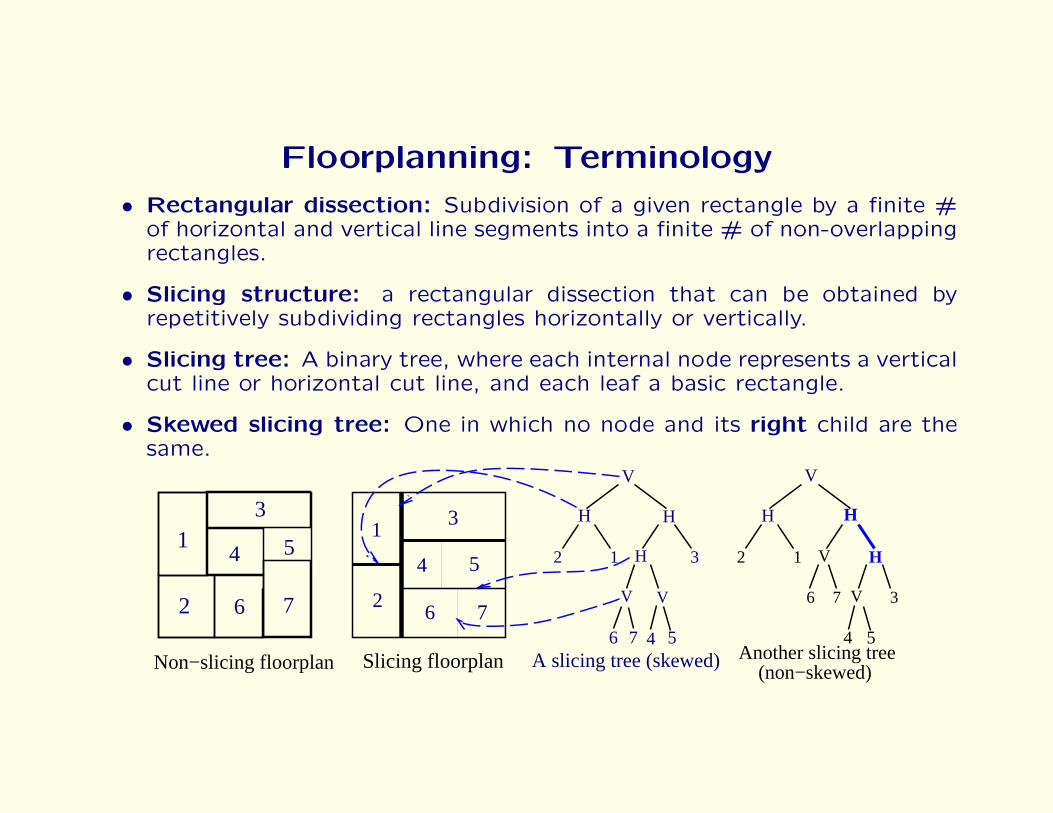
Floorplanning: Terminology
• Rectangular dissection: Subdivision of a given rectangle by a finite #of horizontal and vertical line segments into a finite # of non-overlappingrectangles.
• Slicing structure: a rectangular dissection that can be obtained byrepetitively subdividing rectangles horizontally or vertically.
• Slicing tree: A binary tree, where each internal node represents a verticalcut line or horizontal cut line, and each leaf a basic rectangle.
• Skewed slicing tree: One in which no node and its right child are thesame.
13
4 5
6 72
H
V
H
H
V V
12 3
4 56 7
13
4 5
6 72
A slicing tree (skewed)
H
V
H
HV
V
12
3
4 5
6 7
Another slicing tree (non−skewed)Non−slicing floorplan Slicing floorplan
Floorplan Design by Simulated Annealing
• Related work
– Wong & Liu, “A new algorithm for floorplan design,” DAC’86.
∗ Consider slicing floorplans.
– Wong & Liu, “Floorplan design for rectangular and L-shaped mod-ules,” ICCAD’87.
∗ Also consider L-shaped modules.
– Wong, Leong, Liu, Simulated Annealing for VLSI Design, pp. 31–71,Kluwer academic Publishers, 1988.
• Ingredients: solution space, neighborhood structure, cost function, an-nealing schedule?

jAlgorithms for VLSI Physical Design Automation
����
c Sherwani ��
Partitioning
Simulated Annealing Algorithm
�
� Concept analogous to the annealing process
used for metals and glass�
� A random initial partition is available as input�
� A new partitioning is generated by
exchanging some elements�
� If the partitions improve the move
is always accepted�
� If not then the move is accepted with a
probability which decreases with
the increase in a parameter called temperature T

jAlgorithms for VLSI Physical Design Automation
����
c Sherwani ��
Partitioning
The Annealing curve
Temp
Time
Global Minima
Local Minima’s

jAlgorithms for VLSI Physical Design Automation
����
c Sherwani ��
Partitioning
Simulated Annealing Algorithm
�
Algorithm SA
begint � t��
cur part � ini part�
cur score � SCORE�cur part��
repeat
repeat
comp� � SELECT�part���
comp� � SELECT�part���
trial part � EXCHANGE�comp�� comp�� cur part��
trial score � SCORE�trial part��
�s � trial score � cur score�
if ��s � � then
cur score � trial score�
cur part � MOVE�comp�� comp���
elser � RANDOM� � ���
if �r � e��s
t � then
cur score � trial score�
cur part � MOVE�comp�� comp� ��
until �equilibrium at t is reached�
t � �t �� � � �� ��
until �freezing point is reached�
end�

Solution Representation• An expression E = e1e2 . . . e2n−1, where ei ∈ {1,2, . . . , n,H, V },1 ≤ i ≤
2n− 1, is a Polish expression of length 2n− 1 iff
1. every operand j, 1 ≤ j ≤ n, appears exactly once in E;2. (the balloting property) for every subexpression Ei = e1 . . . ei,1 ≤
i ≤ 2n− 1, #operands > #operators.
1 6 H 3 5 V 2 H V 7 4 H V
# of operands = 4 ....... = 7# of operators = 2 ....... = 5
• Polish expression ←→ Postorder traversal.• ijH: rectangle i on bottom of j; ijV : rectangle i on the left of j.
7 54
21
6
3
V
H H
V V
H 2 7 5
3 4
1 6E = 16H2V75VH34HV
E = 16+2*75*+34+*Postorder traversal of a tree!

Solution Representation (cont’d)
VV
H
1 4
1
43
22 3
E = 123H4VV
V
H
V
3
1
2
4
E = 123HV4V non−skewed! skewed!
H
H
....... HH ........
V
V
....... VV ........
Non−skewed cases
• Question: How to eliminate ambiguous representation?
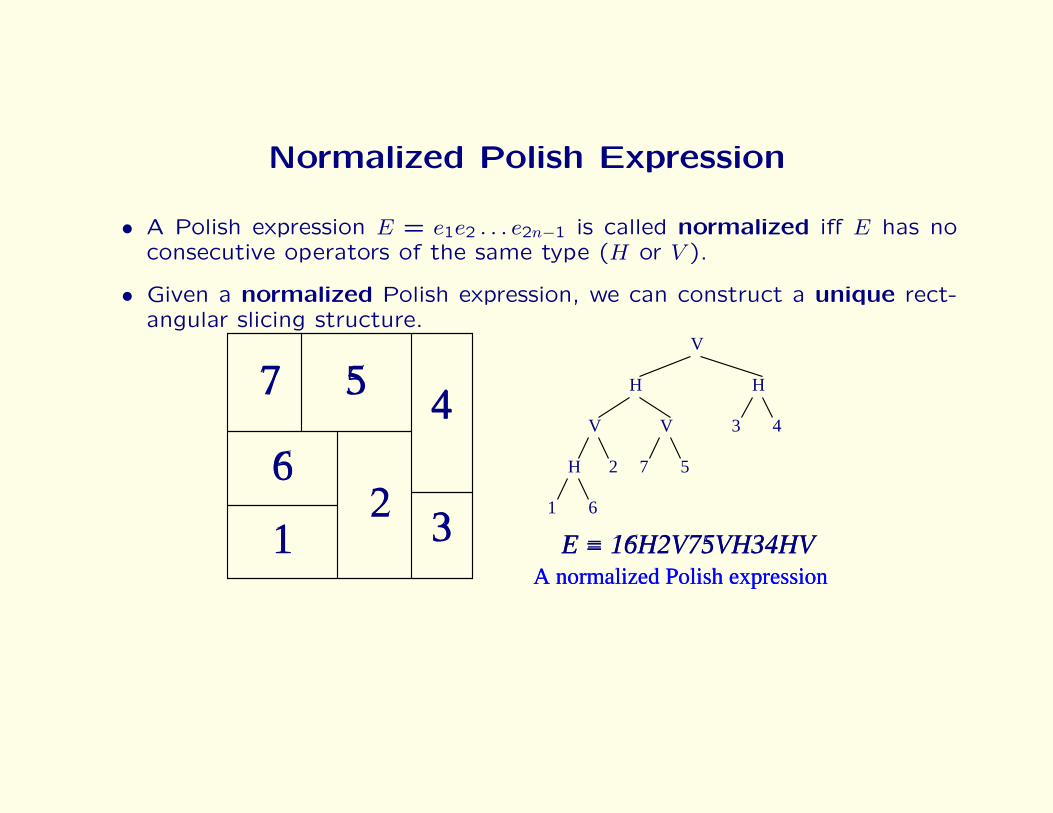
Normalized Polish Expression
• A Polish expression E = e1e2 . . . e2n−1 is called normalized iff E has noconsecutive operators of the same type (H or V ).
• Given a normalized Polish expression, we can construct a unique rect-angular slicing structure.
7 54
21
6
3
V
H H
V V
H 2 7 5
3 4
1 6
E = 16H2V75VH34HVA normalized Polish expression

Neighborhood Structure
• Chain: HVHVH . . . or V HV HV . . .
1 6 H 3 5 V 2 H V 7 4 H V
chain
• Adjacent: 1 and 6 are adjacent operands; 2 and 7 are adjacent operands;5 and V are adjacent operand and operator.
• 3 types of moves:
– M1 (Operand Swap): Swap two adjacent operands.
– M2 (Chain Invert): Complement some chain (V = H,H = V ).
– M3 (Operator/Operand Swap): Swap two adjacent operand andoperator.

Effects of Perturbation
1
2
3
4
2
4
3
1 24
3
1
2
4
3
1
12V4H3V
M1 M2 M3
12V3H4V 12H3H4V 12H34HV
• Question: The balloting property holds during the moves?
– M1 and M2 moves are OK.
– Check the M3 moves! Reject “illegal” M3 moves.
• Check M3 moves: Assume that the M3 move swaps the operand eiwith the operator ei+1, 1 ≤ i ≤ k−1. Then, the swap will not violate theballoting property iff 2Ni+1 < i.
– Nk: # of operators in the Polish expression E = e1e2 . . . ek,1 ≤ k ≤ 2n− 1.

Cost Function• Φ = A+ λW .
– A: area of the smallest rectangle
– W : overall wiring length
– λ: user-specified parameter
1
2
3
4
2
4
3
1 24
3
1
2
4
3
1M1 M2 M3
A: 12H34HV
• W =∑
ij cijdij.
– cij: # of connections between blocks i and j.
– dij: center-to-center distance between basic rectangles i and j.

Area Computation
{ (5,5) (9,4) }
{ (3,2) }
{ (3,5) (6,,4) }{ (2,5) (3,4) }
{ (2,3) (3,2) } { (2,2) }
{ (1,3) (3,1) } { (2,3) (3,2) }
{ (1,2) (2,1) } { (2,2) }
V
HH
V
1 2
3 4
5 6
{ (6,2) (3,3) }
V
1
2 5
3
6
4
2
3
2 1 2
V
HH
V
1 2
3 4
5 6
V
u1 u2
v w
max{u1, u2}
v+w
u1 u2
v wu1
u2
max{v, w}
u1+u2
• Wiring cost?

Incremental Computation of Cost Function
• Each move leads to only a minor modification of the Polish expression.
• At most two paths of the slicing tree need to be updated for each move.
V
HH
V1 2
3 45 6
V
V
HH
V
1 2
36
V
E = 12H34V56VHV
M1
E = 12H35V46VHV
54

Incremental Computation of Cost Function
(cont’d)
HH
V1 2
3 4
5 6
V
H
1 2
36
V
E = 12H34V56VHV
V
HH
V1 2
3 4
5 6
V
V
H
V
6
V
1
2 3E = 12H34V56VHV
M2
M3
V
E = 12H34V56HVH
H
V
H
H
54
E = 123H4V56VHV
45

Annealing Schedule
• Initial solution: 12V 3V . . . nV .
1 2 3 n
• Ti = riT0, i = 1,2,3, . . .; r = 0.85.
• At each temperature, try kn moves (k = 5–10).
• Terminate the annealing process if
– # of accepted moves < 5%,
– temperature is low enough, or
– run out of time.
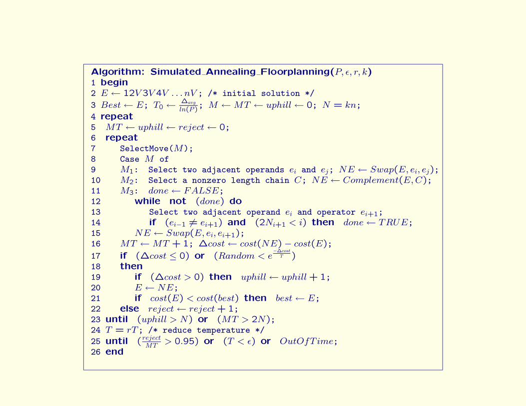
Algorithm: Simulated Annealing Floorplanning(P, ε, r, k)1 begin2 E ← 12V 3V 4V . . . nV ; /* initial solution */
3 Best← E; T0 ← ∆avg
ln(P ); M ←MT ← uphill← 0; N = kn;
4 repeat5 MT ← uphill← reject← 0;6 repeat7 SelectMove(M);8 Case M of9 M1: Select two adjacent operands ei and ej; NE ← Swap(E, ei, ej);10 M2: Select a nonzero length chain C; NE ← Complement(E,C);11 M3: done← FALSE;12 while not (done) do13 Select two adjacent operand ei and operator ei+1;14 if (ei−1 6= ei+1) and (2Ni+1 < i) then done← TRUE;15 NE ← Swap(E, ei, ei+1);16 MT ←MT + 1; ∆cost← cost(NE)− cost(E);
17 if (∆cost ≤ 0) or (Random < e−∆cost
T )18 then19 if (∆cost > 0) then uphill← uphill + 1;20 E ← NE;21 if cost(E) < cost(best) then best← E;22 else reject← reject+ 1;23 until (uphill > N) or (MT > 2N);24 T = rT; /* reduce temperature */
25 until (rejectMT
> 0.95) or (T < ε) or OutOfT ime;26 end

Practical Problems in VLSI Physical Design Polish Expression (1/8)
Draw slicing floorplan based on:Initial PE: P1 = 25V1H374VH6V8VHDimensions: (2,4), (1,3), (3,3), (3,5), (3,2), (5,3), (1,2), (2,4)
Normalized Polish Expression

Practical Problems in VLSI Physical Design Polish Expression (2/8)
M1 MoveSwap module 3 and 7 in P1 = 25V1H374VH6V8VH
We get: P2 = 25V1H734VH6V8VHArea changed from 11 × 15 to 13 × 14
Practical Problems in VLSI Physical Design Polish Expression (3/8)
Change on Floorplan

Practical Problems in VLSI Physical Design Polish Expression (4/8)
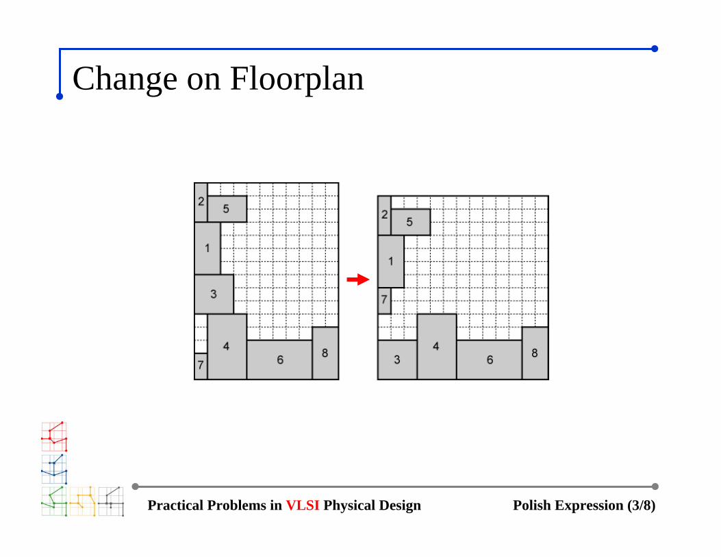
M2 MoveComplement last chain in P2 = 25V1H734VH6V8VH
We get: P3 = 25V1H734VH6V8HVArea changed from 13 × 14 to 15 × 11

Practical Problems in VLSI Physical Design Polish Expression (5/8)
Change on Floorplan
Practical Problems in VLSI Physical Design Polish Expression (6/8)
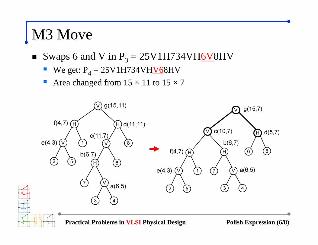
M3 MoveSwaps 6 and V in P3 = 25V1H734VH6V8HV
We get: P4 = 25V1H734VHV68HVArea changed from 15 × 11 to 15 × 7

Practical Problems in VLSI Physical Design Polish Expression (7/8)
Change on Floorplan

Practical Problems in VLSI Physical Design Polish Expression (8/8)
Initial Temperature CalculationWhat is average change on cost function?Initial temperature with acceptance probability 0.9?

• A calculator company produces a scientific calculator and a graphing calculator.
• Long-term projections indicate an expected demand of at least 100 scientific and 80 graphing calculators each day.
• Because of limitations on production capacity, no more than 200 scientific and 170 graphing calculators can be made daily.
• To satisfy a shipping contract, a total of at least 200 calculators must be shipped each day.
• If each scientific calculator sold results in a $2 loss, but each graphing calculator produces a $5 profit, how many of each type should be made daily to maximize net profits?
Sample LP Problem

• Variables– x: number of scientific calculators produced– y: number of graphing calculators produced
• Objective function– P = –2x + 5y
• Constraints– 100 < x < 200 – 80 < y < 170 – y > –x + 200
• Answer– P = 650 at (x, y) = (100, 170)
LP Formulation

Linear program (LP)
minimize
n∑
j=1
cjxj
subject to
n∑
j=1
aijxj ≤ bi, i = 1, . . . ,m
n∑
j=1
cijxj = di, i = 1, . . . , p
variables: xj; problem data: cj, aij, bi, cij, di
properties
• can be solved very efficiently (several 10,000 variables, constraints)• widely available general-purpose software• extensive, useful theory, e.g., can characterize sensitivity of optimumwith respect to changes in data
Introduction and overview 1–2

Integer linear program
integer linear program
minimize∑n
j=1 cjxj
subject to∑n
j=1 aijxj ≤ bi, i = 1, . . . ,m∑nj=1 cijxj = di, i = 1, . . . , p
xj ∈ Z
Boolean linear program
minimize∑n
j=1 cjxj
subject to∑n
j=1 aijxj ≤ bi, i = 1, . . . ,m∑nj=1 cijxj = di, i = 1, . . . , p
xj ∈ {0, 1}
• very general problems; can be extremely hard to solve• can be solved as a sequence of linear programs
Introduction and overview 1–8

Floorplanning by Mathematical Programming
• Sutanthavibul, Shragowitz, and Rosen, “An analytical approach to floor-plan design and optimization,” 27th DAC, 1990.
• Notation:
– wi, hi: width and height of module Mi.
– (xi, yi): coordinate of the lower left corner of module Mi.
– ai ≤ wi/hi ≤ bi: aspect ratio wi/hi of module Mi. (Note: We definedaspect ratio as hi/wi before.)
• Goal: Find a mixed integer linear programming (ILP) formulation forthe floorplan design.
– Linear constraints? Objective function?

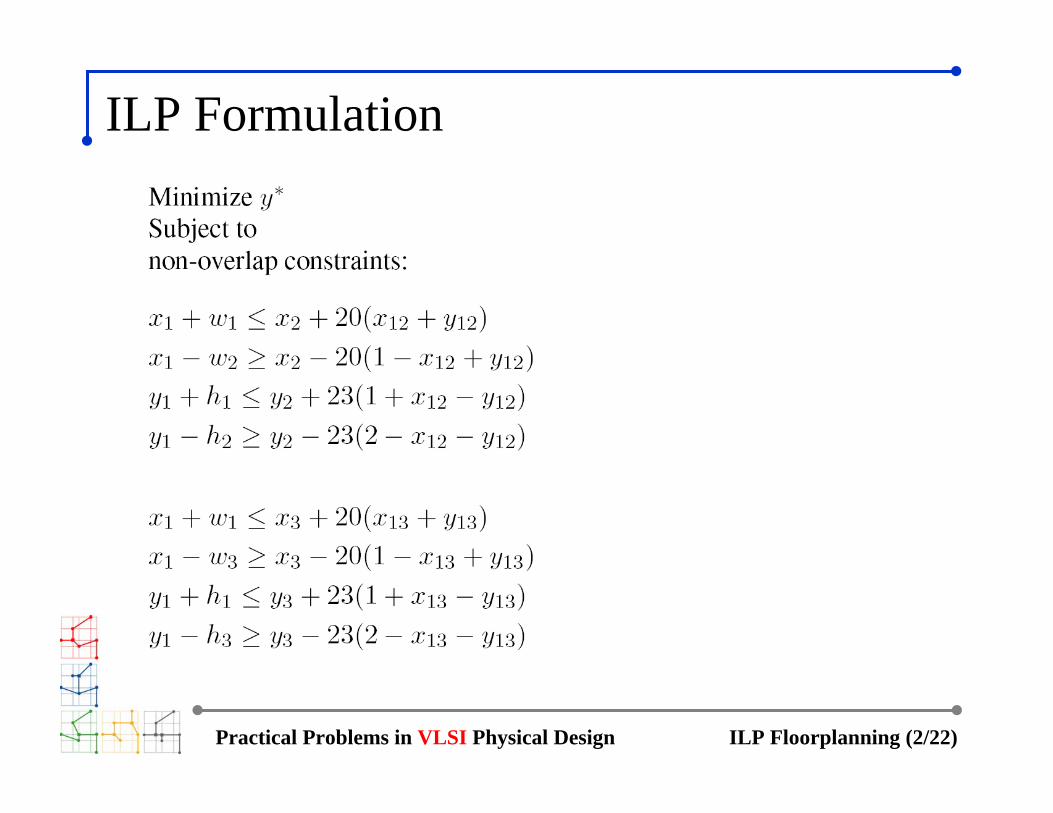
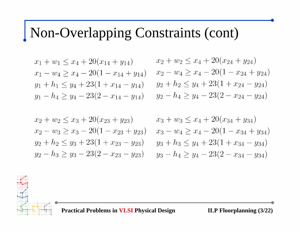
Nonoverlap Constraints
• Two modules Mi and Mj are nonoverlap, if at least one of the following linear constraintsis satisfied (cases encoded by pij and qij):
pij qijMi to the left of Mj: xi + wi ≤ xj 0 0Mi below Mj: yi + hi ≤ yj 0 1Mi to the right of Mj: xi − wj ≥ xj 1 0Mi above Mj: yi − hj ≥ yj 1 1
• Let W,H be upper bounds on the floorplan width and height, respectively.
• Introduce two 0,1 variables pij and qij to denote that one of the above inequalities isenforced; e.g., pij = 0, qij = 1⇒ yi + hi ≤ yj is satisfied.
xi + wi ≤ xj +W (pij + qij)
yi + hi ≤ yj +H(1 + pij − qij)xi − wj ≥ xj −W (1− pij + qij)
yi − hj ≥ yj −H(2− pij − qij)
(xi, yi) (xj, yj)
wi
xi + wi <= xj(xi, yi) (xj, yj)
wi
xi + wi > xj
hi
wjhj
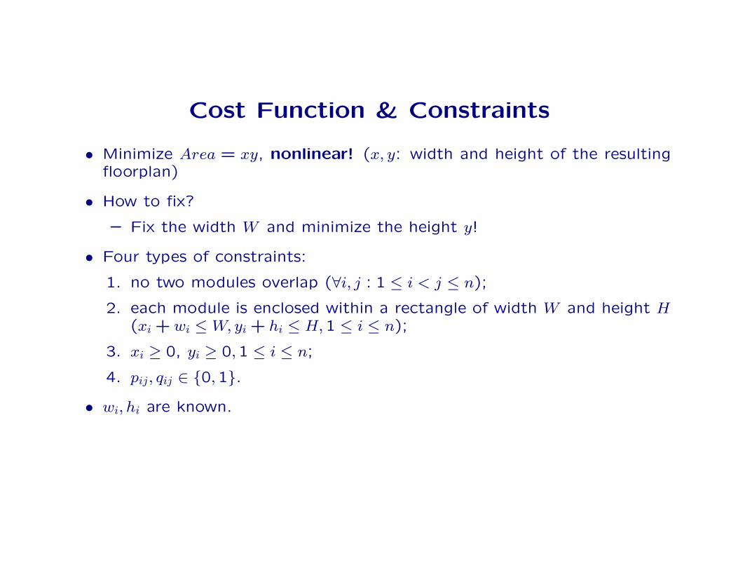
Cost Function & Constraints
• Minimize Area = xy, nonlinear! (x, y: width and height of the resultingfloorplan)
• How to fix?
– Fix the width W and minimize the height y!
• Four types of constraints:
1. no two modules overlap (∀i, j : 1 ≤ i < j ≤ n);
2. each module is enclosed within a rectangle of width W and height H(xi + wi ≤W, yi + hi ≤ H,1 ≤ i ≤ n);
3. xi ≥ 0, yi ≥ 0,1 ≤ i ≤ n;
4. pij, qij ∈ {0,1}.
• wi, hi are known.

Mixed ILP for Floorplanning
Mixed ILP for the floorplanning problem with rigid, fixed modules.
min y
subject to
xi + wi ≤W, 1 ≤ i ≤ n (1)
yi + hi ≤ y, 1 ≤ i ≤ n (2)
xi + wi ≤ xj +W (pij + qij), 1 ≤ i < j ≤ n (3)
yi + hi ≤ yj +H(1 + pij − qij), 1 ≤ i < j ≤ n (4)
xi − wj ≥ xj −W (1− pij + qij), 1 ≤ i < j ≤ n (5)
yi − hj ≥ yj −H(2− pij − qij), 1 ≤ i < j ≤ n (6)
xi, yi ≥ 0, 1 ≤ i ≤ n (7)
pij, qij ∈ {0,1}, 1 ≤ i < j ≤ n (8)
• Size of the mixed ILP: for n modules,
– # continuous variables: O(n); # integer variables: O(n2); # linear constraints:O(n2).
– Unacceptably huge program for a large n! (How to cope with it?)
• Popular LP software: LINDO, lp solve, etc.

Mixed ILP for Floorplanning (cont’d)
Mixed ILP for the floorplanning problem: rigid, freely oriented modules.
min y
subject to
xi + rihi + (1− ri)wi ≤W, 1 ≤ i ≤ n (9)
yi + riwi + (1− ri)hi ≤ y, 1 ≤ i ≤ n (10)
xi + rihi + (1− ri)wi ≤ xj +M(pij + qij), 1 ≤ i < j ≤ n (11)
yi + riwi − (1− ri)hi ≤ yj +M(1 + pij − qij), 1 ≤ i < j ≤ n (12)
xi − rjhj + (1− rj)wj ≥ xj −M(1− pij + qij), 1 ≤ i < j ≤ n (13)
yi − rjwj − (1− rj)hj ≥ yj −M(2− pij − qij), 1 ≤ i < j ≤ n (14)
xi, yi ≥ 0, 1 ≤ i ≤ n (15)
pij, qij ∈ {0,1}, 1 ≤ i < j ≤ n (16)
• For each module i with free orientation, associate a 0-1 variable ri:
– ri = 0: 0◦ rotation for module i.
– ri = 1: 90◦ rotation for module i.
• M = max{W,H}.

Flexible Modules
• Assumptions: wi, hi are unknown; area lower bound: Ai.
• Module size constraints: wihi ≥ Ai; ai ≤ wihi≤ bi.
• Hence, wmin =√Aiai, wmax =
√Aibi, hmin =
√Ai
bi, hmax =
√Ai
ai.
• wihi ≥ Ai nonlinear! How to fix?
– Can apply a first-order approximation of the equation: a line passing through(wmin, hmax) and (wmax, hmin).
hi = ∆iwi + ci / ∗ y = mx+ c ∗ /
∆i =hmax − hminwmin − wmax
/ ∗ slope ∗ /
ci = hmax −∆iwmin / ∗ c = y0 −mx0 ∗ /
– Substitute ∆iwi+ ci for hi to form linear constraints (xi, yi, wi are unknown; ∆i,ci, can be computed as above).

Wirelength Constraint
• Critical nets– Timing analysis, power analysis, etc
• 6 new continuous variables per net– Half perimeter of bounding box of each net is bounded
– Overhead is not significant: time dependence on # of continuous variable is at most linear
nnnnnnnnn
inin
inin
Lyxyyyxxxniyyniyynixxnixx
≤+−≥−≥
∈∀=∈∀=
∈∀=∈∀=
,ˆ,ˆminˆ,maxminˆ,max

Reducing the Size of the Mixed ILP
• Time complexity of a mixed ILP: exponential!
• Recall the large size of the mixed ILP: # variables, # constraints: O(n2).
– How to fix it?
• Key: Solve a partial problem at each step (successive augmentation)
• Questions:
– How to select next subgroup of modules? ⇒ linear ordering based on connectivity.
– How to minimize the # of required variables?

W
Partial floorplan
Next group of modules
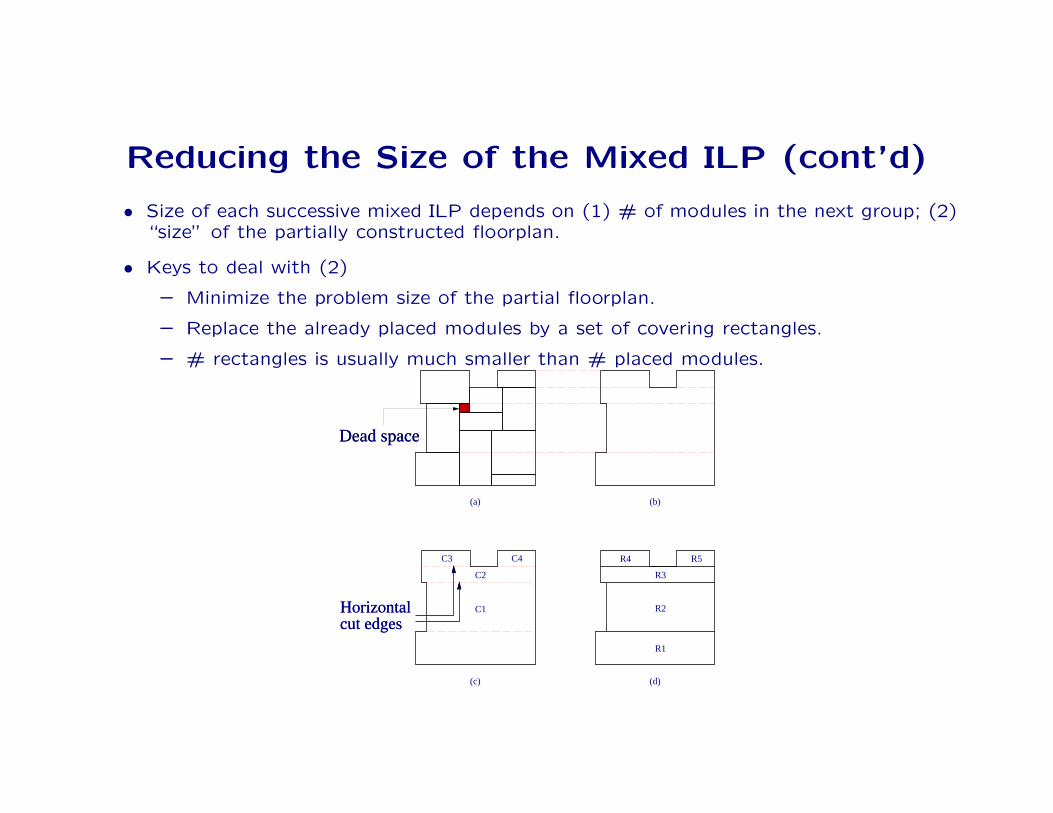
Reducing the Size of the Mixed ILP (cont’d)
• Size of each successive mixed ILP depends on (1) # of modules in the next group; (2)“size” of the partially constructed floorplan.
• Keys to deal with (2)
– Minimize the problem size of the partial floorplan.
– Replace the already placed modules by a set of covering rectangles.
– # rectangles is usually much smaller than # placed modules.
Dead space
(a) (b)
(c)
Horizontal cut edges
C3 C4
C2
C1
(d)
R4 R5
R3
R2
R1

Practical Problems in VLSI Physical Design ILP Floorplanning (1/22)
Fixed modules only, no rotation allowedm1 (4,5), m2 (3,7), m3 (6,4), m4 (7,7)
I. Floorplanning with Fixed Modules
Practical Problems in VLSI Physical Design ILP Floorplanning (2/22)
ILP Formulation
Practical Problems in VLSI Physical Design ILP Floorplanning (3/22)
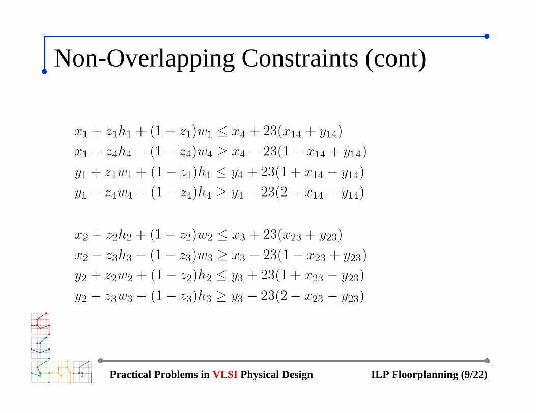
Non-Overlapping Constraints (cont)

Practical Problems in VLSI Physical Design ILP Floorplanning (4/22)
Additional Constraints
Practical Problems in VLSI Physical Design ILP Floorplanning (5/22)
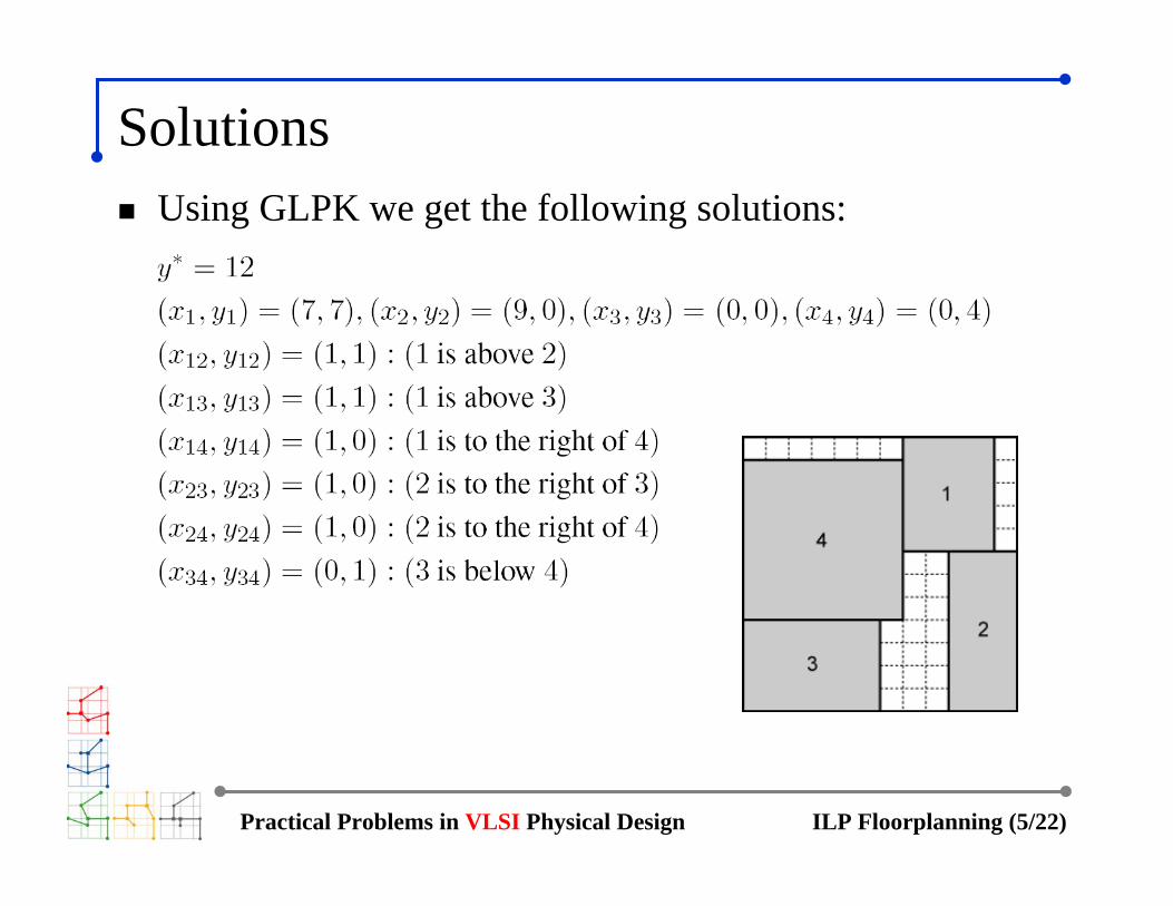
SolutionsUsing GLPK we get the following solutions:

Practical Problems in VLSI Physical Design ILP Floorplanning (6/22)
Final FloorplanWhy the non-optimality?
Due to linear approximation of area objective (= y*)Chip width/height constraints also affectedIn fact, our ILP solution (y* = 12) is optimal under these conditions.

Practical Problems in VLSI Physical Design ILP Floorplanning (7/22)
II. Floorplanning with RotationFixed modules, rotation allowed
Fixed modules: m1 (4,5), m2 (3,7), m3 (6,4), m4 (7,7)Need 4 more binary variables for rotation: z1, z2, z3, z4
We use M = max{W,H} = 23

Practical Problems in VLSI Physical Design ILP Floorplanning (8/22)
ILP Formulation
Practical Problems in VLSI Physical Design ILP Floorplanning (9/22)
Non-Overlapping Constraints (cont)
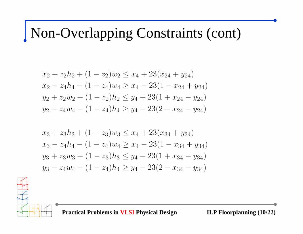
Practical Problems in VLSI Physical Design ILP Floorplanning (10/22)
Non-Overlapping Constraints (cont)

Practical Problems in VLSI Physical Design ILP Floorplanning (11/22)
Additional Constraints
Practical Problems in VLSI Physical Design ILP Floorplanning (12/22)
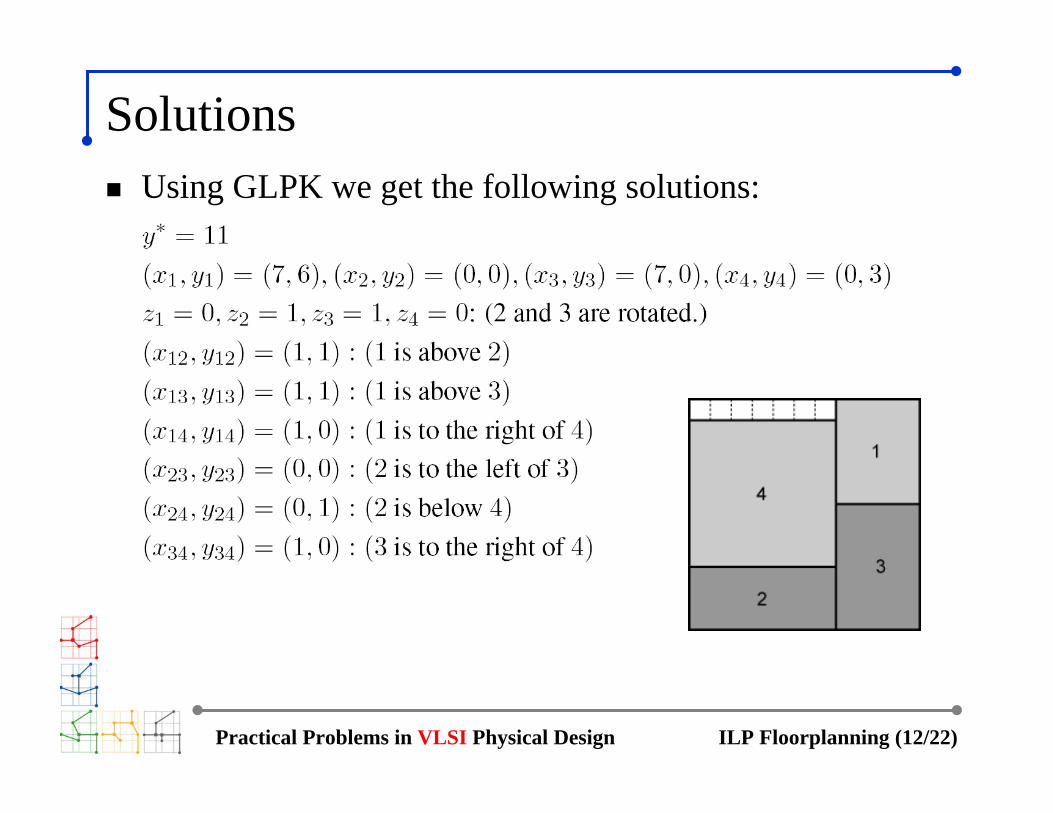
SolutionsUsing GLPK we get the following solutions:

Practical Problems in VLSI Physical Design ILP Floorplanning (13/22)
III. Floorplanning with Flexible Modules2 Fixed modules:
m1 (4,5), m2 (3,7) (rotation allowed)
2 Flexible modules: m3: area = 24, aspect ratio [0.5, 2]m4: area = 49, aspect ratio [0.3, 2.5]
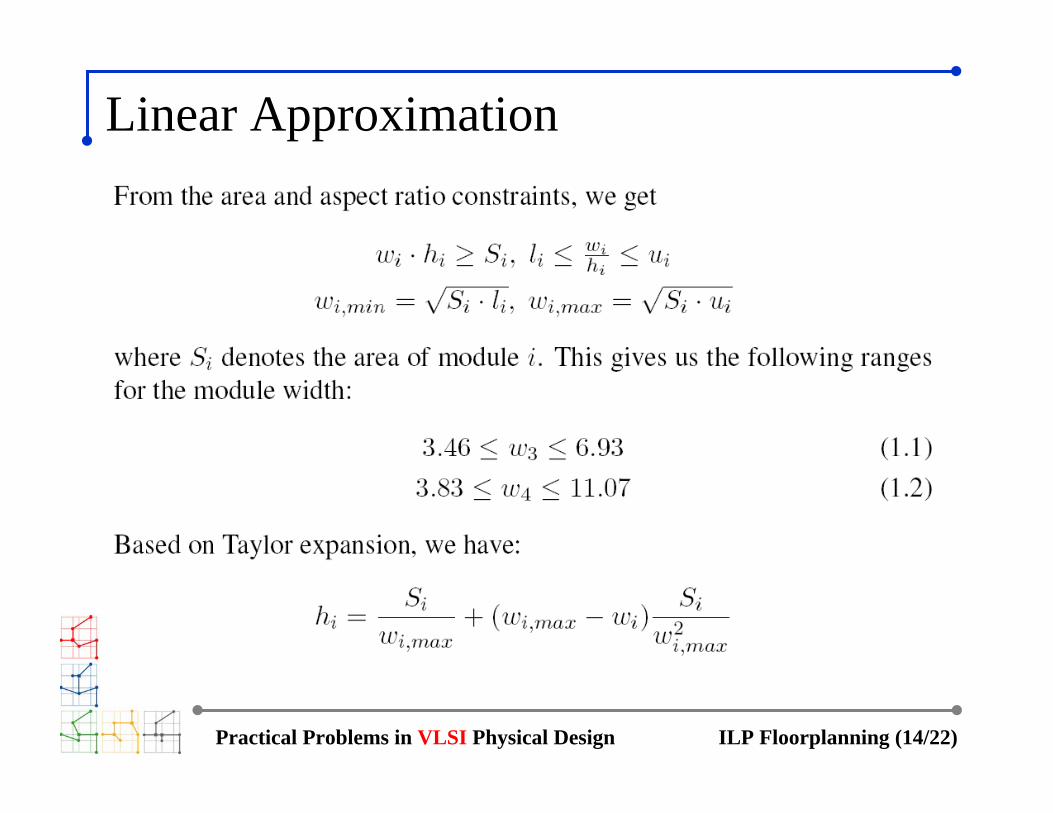
Practical Problems in VLSI Physical Design ILP Floorplanning (14/22)
Linear Approximation

Practical Problems in VLSI Physical Design ILP Floorplanning (15/22)
Linear Approximation (cont)

Practical Problems in VLSI Physical Design ILP Floorplanning (16/22)
Upper Bound of Chip Dimension
Practical Problems in VLSI Physical Design ILP Floorplanning (17/22)
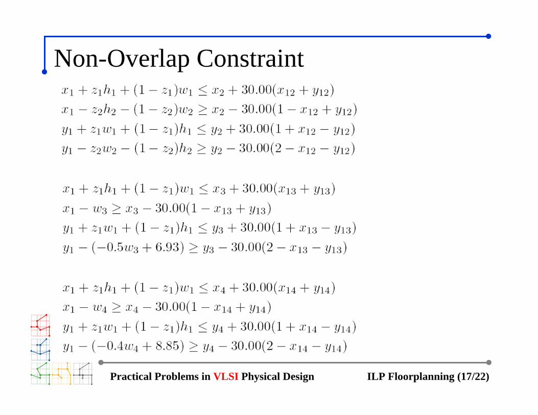
Non-Overlap Constraint
Practical Problems in VLSI Physical Design ILP Floorplanning (18/22)
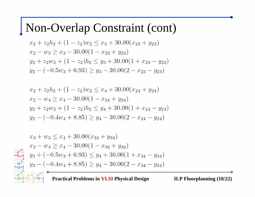
Non-Overlap Constraint (cont)
Practical Problems in VLSI Physical Design ILP Floorplanning (19/22)
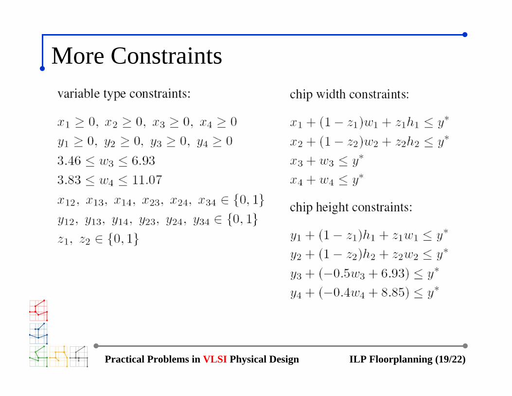
More Constraints
Practical Problems in VLSI Physical Design ILP Floorplanning (20/22)
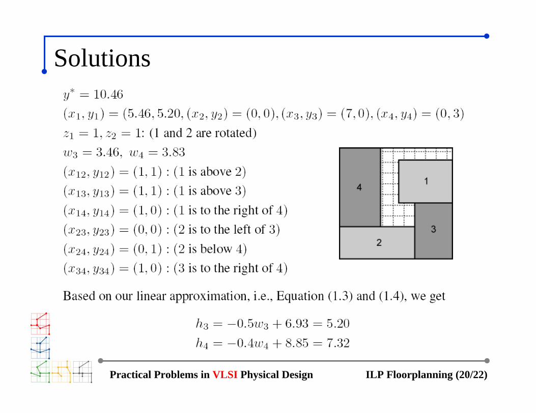
Solutions

Practical Problems in VLSI Physical Design ILP Floorplanning (21/22)
ComparisonFixed modules only = 12 × 12Rotation allowed = 11 × 11Flexible modules used = 10.46 × 10.32

Practical Problems in VLSI Physical Design ILP Floorplanning (22/22)
Approximation Error and OverlapDue to linear approximation
Approximated area of m3 = 3.46 × 5.2 = 17.99 (actually 24)Approximated area of m4 = 3.83 × 7.32 = 28.04 (actually 49)Real area of m3 = 3.46 × 6.94 = 24Real area of m4 = 3.83 × 12.79 = 49Floorplan area increases, overlap occurs

P-admissible Solution Space
• P-admissible solution space for Problem P:
1. the solution space is finite,
2. every solution is feasible,
3. evaluation for each configuration is possible in polynomial time andso is the implementation of the corresponding configuration, and
4. the configuration corresponding to the best evaluated solution in thespace coincides with an optimal solution of P.
• Slicing floorplan is not P-admissible. Why?
• A P-admissible floorplan representation: Sequence Pair.
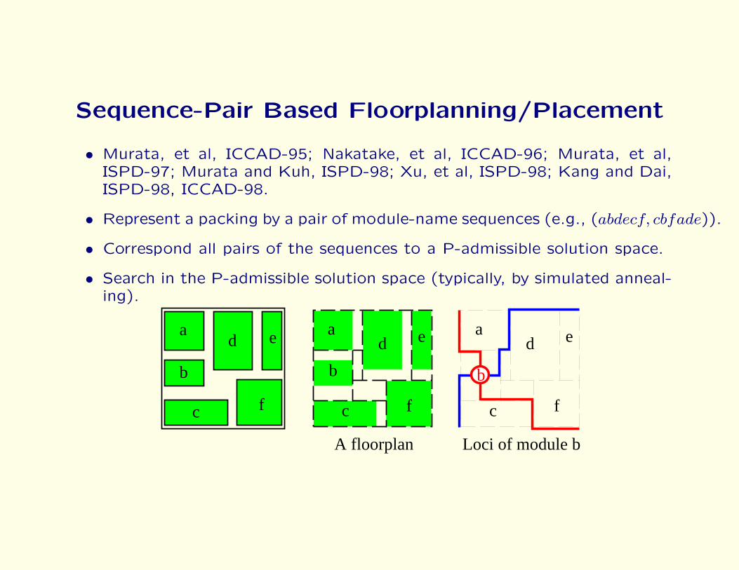
Sequence-Pair Based Floorplanning/Placement
• Murata, et al, ICCAD-95; Nakatake, et al, ICCAD-96; Murata, et al,ISPD-97; Murata and Kuh, ISPD-98; Xu, et al, ISPD-98; Kang and Dai,ISPD-98, ICCAD-98.
• Represent a packing by a pair of module-name sequences (e.g., (abdecf, cbfade)).
• Correspond all pairs of the sequences to a P-admissible solution space.
• Search in the P-admissible solution space (typically, by simulated anneal-ing).
b
c
d e
f
a
b
c
d e
f
a
c
d e
f
a
b
Loci of module bA floorplan

Relative Module Positions• A floorplan is a partition of a chip into rooms, each containing at most
one block.
• Locus (right-up, left-down, up-left, down-right)
1. Take a non-empty room.
2. Start at the center of the room, walk in two alternating directions tohit the sides of rooms.
3. Continue until to reach a corner of the chip.
• Positive locus: Union of right-up locus and left-down locus.
• Negative locus: Union of up-left locus and down-right locus.
b
d e
fc
a
b
d e
fc
a
Positive loci: abdecf Negative loci: cbfade
c
d e
f
a
b
Loci of module b

Geometrical Information
• No pair of positive (negative) loci cross each other, i.e., loci are linearlyordered.
• Sequence Pair (Γ+,Γ−): Γ+ is a module-name sequence representingthe order of positive loci. (Exp: (Γ+,Γ−) = (abdecf, cbfade))
• x′ is after (before) x in both Γ+ and Γ− =⇒ x′ is right (left) to x.
• x′ is after (before) x in Γ+ and before (after) x in Γ− =⇒ x′ is below(above) x.
b
d e
fc
a
b
d e
fc
a
Positive loci: abdecf Negative loci: cbfade
c
d e
f
a
b
Loci of module b

(Γ+,Γ−)-Packing
• For every sequence pair (Γ+,Γ−), there is a (Γ+,Γ−) packing.
• Horizontal constraint graph GH(V,E) (similarly for GV (V,E)):
– V : source s, sink t, m vertices for modules.
– E: (s, x) and (x, t) for each module x, and (x, x′) iff x must be left-tox′.
– Vertex weight: 0 for s and t, width of module x for the othervertices.
b
d e
fc
a
b
d e
fc
a
Horizontal constraint graph(Transitive edges are not shown)
b
d e
fc
a
Vertical constraint graph(Transitive edges are not shown)
Packing for sequence pair: (abdecf, cbfade)
s t
s
t

Optimal (Γ+,Γ−)-Packing
• Optimal (Γ+,Γ−)-Packing can be obtained in O(m2) time by applyinga longest path algorithm on a vertex-weighted directed acyclic graph.
– GH and GV are independent.
– The X and Y coordinates of each module are determined as theminimum by assigning the longest path length between s and thevertex of the module in GH and GV , respectively.
• The set of all sequence pairs is a P-admissible solution space.
b
d e
fc
a
b
d e
fc
a
Horizontal constraint graph(Transitive edges are not shown)
b
d e
fc
a
Vertical constraint graph(Transitive edges are not shown)
Packing for sequence pair: (abdecf, cbfade)
s t
s
t
Sequence Pair
• Final chip area?• Solution space size?
– Without rotation vs with rotation
• Optimization: Simulated Annealing– Initial solution: Γ+ = Γ-
– Swap two modules in Γ+
– Swap two modules both in Γ+ and Γ-
– Rotate
• Results: produces highly packed non-slicing floorplans

Annealing Temperature vs. Floorplan Quality
(c) temperature: 20area: 7260120
3549
2696
3111
4174
(a) temperature: 2000area: 12985314
(b) temperature: 1000area: 9568104
2814
2580
-26.3%
-44.1%
m0
m1
m2
m3
m4
m5
m6m7m10
m13
m8
m11m12 m9
m8
m8
m3m3 m9
m9
m13 m13 m2
m2 m1 m1m6
m6m7
m5
m11m4

• Floorplan (a)– S1: 11 0 7 10 8 4 1 5 12 2 9 13 6 3– S2: 7 10 6 1 11 5 4 0 13 12 9 2 3 8
• Floorplan (b)– S1: 8 6 13 3 9 5 2 4 10 0 7 12 1 11– S2: 5 6 2 1 8 9 13 4 12 10 11 0 3 7
• Floorplan (c)– S1: 3 11 6 9 5 4 7 0 10 12 13 1 2 8– S2: 1 6 8 12 3 7 5 10 0 9 11 13 4 2
Sequence Pair

Non Slicing Floorplan• Sequence Pair + SA by Adam & Todd (class project)
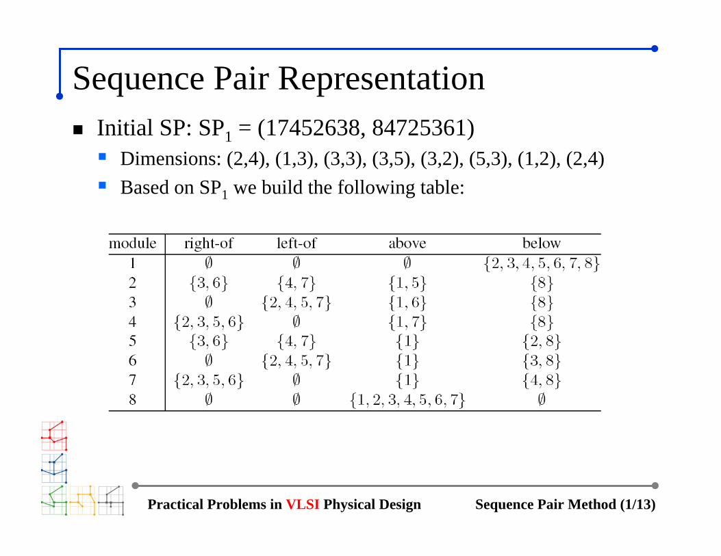
Practical Problems in VLSI Physical Design Sequence Pair Method (1/13)
Initial SP: SP1 = (17452638, 84725361)Dimensions: (2,4), (1,3), (3,3), (3,5), (3,2), (5,3), (1,2), (2,4)Based on SP1 we build the following table:
Sequence Pair Representation

Practical Problems in VLSI Physical Design Sequence Pair Method (2/13)
Constraint GraphsHorizontal constraint graph (HCG)
Before and after removing transitive edges

Practical Problems in VLSI Physical Design Sequence Pair Method (3/13)
Constraint Graphs (cont)Vertical constraint graph (VCG)

Practical Problems in VLSI Physical Design Sequence Pair Method (4/13)
Computing Chip Width and HeightLongest source-sink path length in:
HCG = chip width, VCG = chip heightNode weight = module width/height
Practical Problems in VLSI Physical Design Sequence Pair Method (5/13)
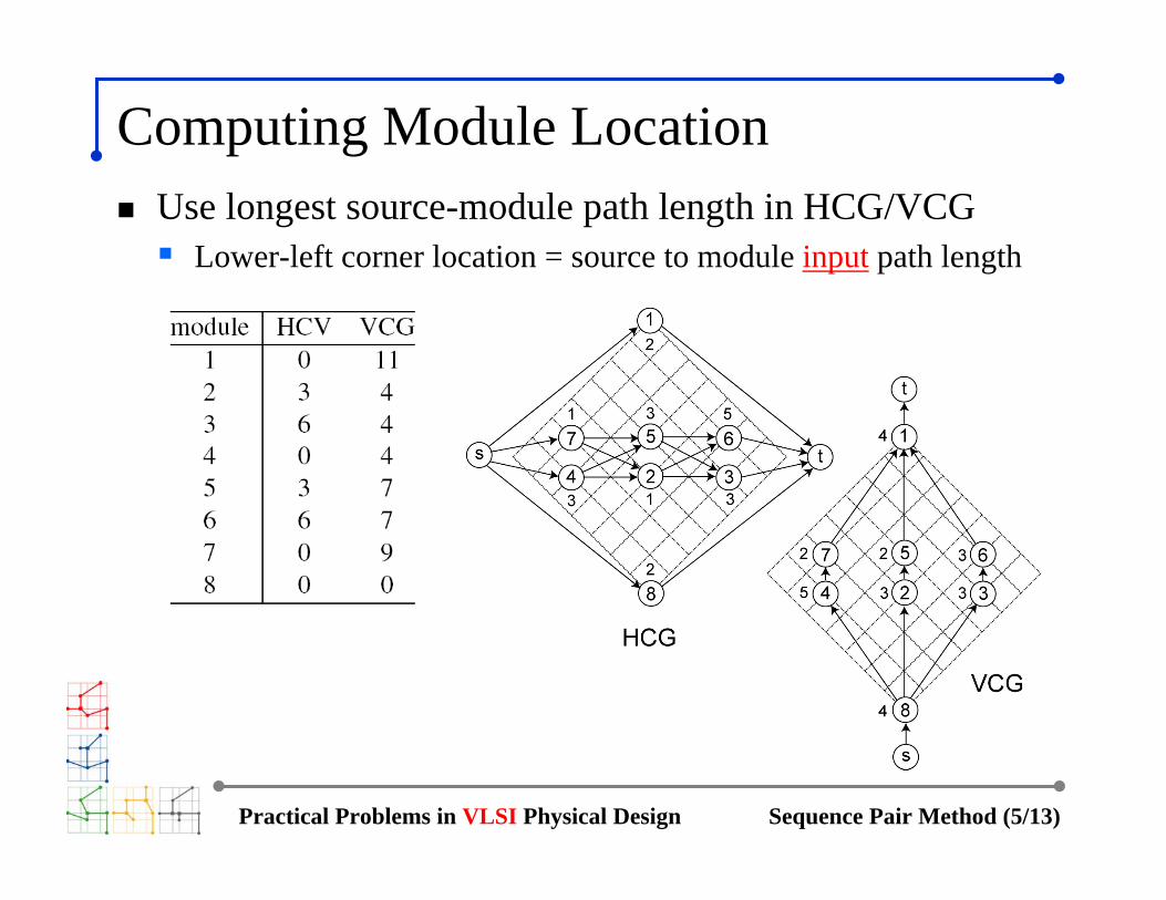
Computing Module LocationUse longest source-module path length in HCG/VCG
Lower-left corner location = source to module input path length
Practical Problems in VLSI Physical Design Sequence Pair Method (6/13)
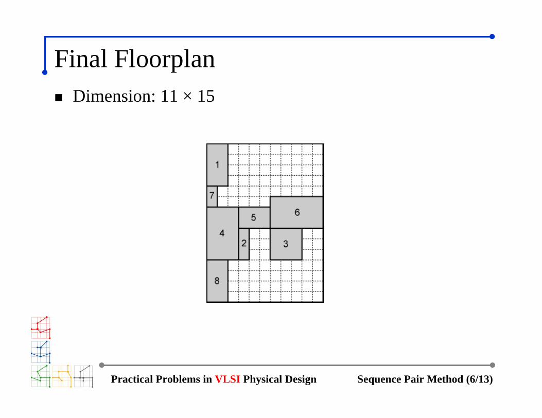
Final FloorplanDimension: 11 × 15
Practical Problems in VLSI Physical Design Sequence Pair Method (7/13)
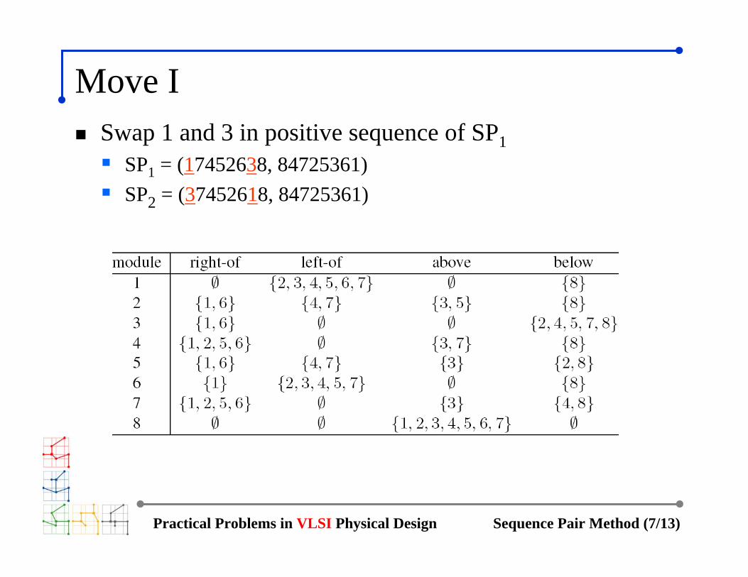
Move ISwap 1 and 3 in positive sequence of SP1
SP1 = (17452638, 84725361)SP2 = (37452618, 84725361)
Practical Problems in VLSI Physical Design Sequence Pair Method (8/13)
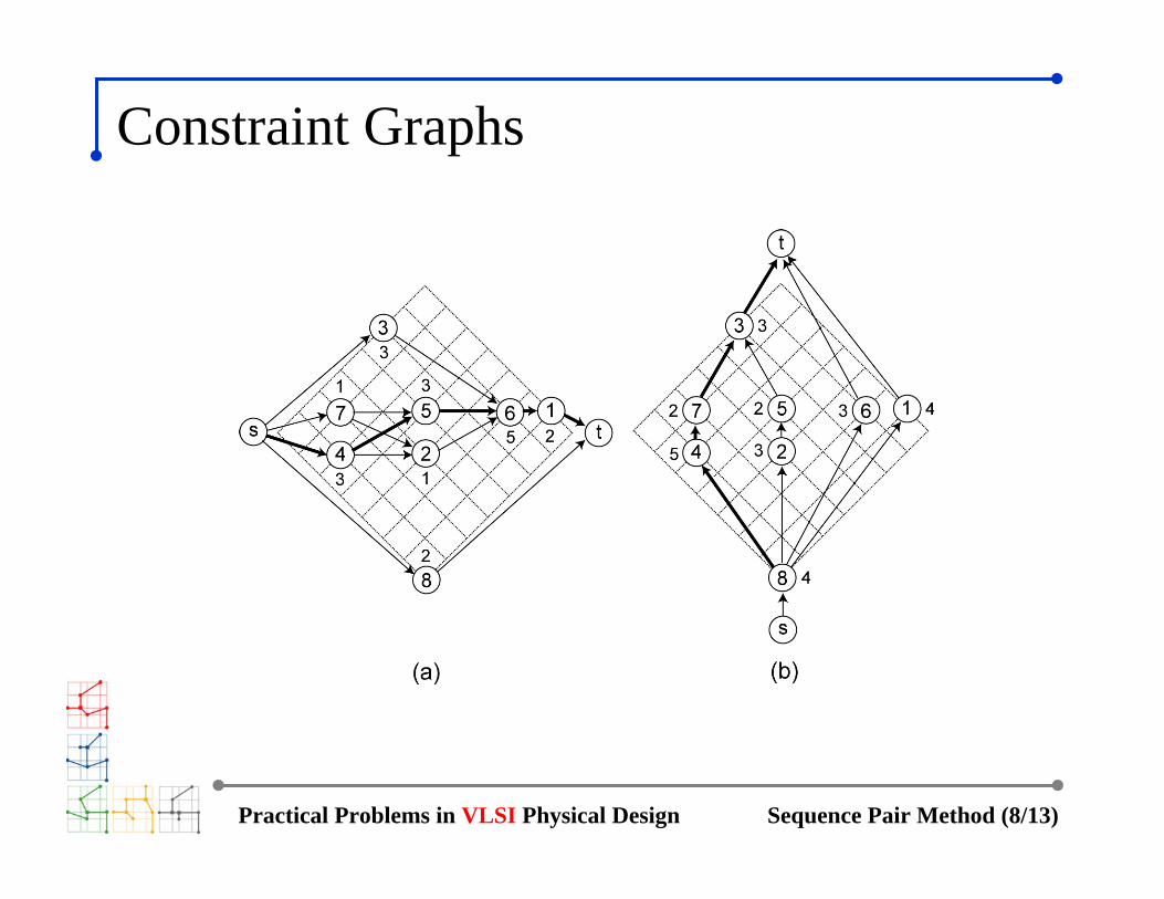
Constraint Graphs

Practical Problems in VLSI Physical Design Sequence Pair Method (9/13)
Constructing FloorplanDimension: 13 × 14

Practical Problems in VLSI Physical Design Sequence Pair Method (10/13)
Move IISwap 4 and 6 in both sequences of SP2
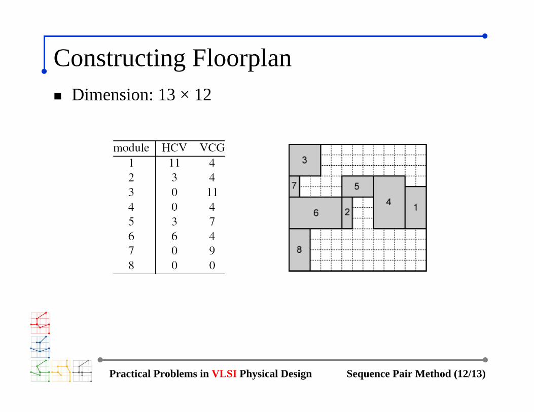
SP2 = (37452618, 84725361)SP3 = (37652418, 86725341)

Practical Problems in VLSI Physical Design Sequence Pair Method (11/13)
Constraint Graphs
Practical Problems in VLSI Physical Design Sequence Pair Method (12/13)
Constructing FloorplanDimension: 13 × 12

Practical Problems in VLSI Physical Design Sequence Pair Method (13/13)
SummaryImpact of the moves:
Floorplan dimension changes from 11 × 15 to 13 × 14 to 13 × 12
Top Related