


Languages
Pages
Legal


Correlative Microscopy in Materials Science
Essential Knowledge Briefings First Edition, 2017
Correlative Microscopy in Materials Science2
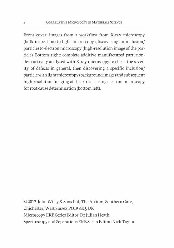
Front cover: images from a workflow from X-ray microscopy (bulk inspec tion) to light microscopy (discovering an inclusion/particle) to electron microscopy (high-resolution image of the par-ticle). Bottom right: complete additive manufactured part, non- destructively analysed with X-ray microscopy to check the sever-ity of defects in general, then discovering a specific inclusion/particle with light microscopy (background image) and subsequent high- resolution imaging of the particle using electron microscopy for root cause determination (bottom left).
© 2017 John Wiley & Sons Ltd, The Atrium, Southern Gate, Chichester, West Sussex PO19 8SQ, UKMicroscopy EKB Series Editor: Dr Julian HeathSpectroscopy and Separations EKB Series Editor: Nick Taylor

Correlative Microscopy in Materials Science 3
About Essential Knowledge BriefingsEssential Knowledge Briefings, published by John Wiley & Sons, comprise a series of short guides to the latest techniques, appli-cations and equipment used in analytical science. Revised and updated annually, EKBs are an essential resource for scientists working in both academia and industry looking to update their understanding of key developments within each specialty. Free to download in a range of electronic formats, the EKB range is available at www.essentialknowledgebriefings.com
CONTENTS4 INTRODUCTION6 HISTORY AND BACKGROUND12 IN PRACTICE24 PROBLEMS AND SOLUTIONS29 WHAT’S NEXT?
Correlative Microscopy in Materials Science4
INTRODUCTION Correlative microscopy is not a single technique but a varied collection of techniques that share a common approach. By apply-ing several different microscopy techniques to a single sample, scientists can study it at a much broader range of magnifications than is possible with a single technique. This allows them to con-duct an initial low-magnification inspection of a sample to identify specific regions of interest (ROIs), which they can then zoom in on for a more detailed analysis, saving time and expense. There are other important advantages as well. Correlative microscopy allows scientists to study a greater diversity of samples, as some micros -copy techniques work better with some materials than others, and to generate a much greater range of information about those sam-ples at various different scales. Combinations of light microscopy and electron microscopy are the most common form of correlative microscopy in use today. But researchers are increasingly designing correlative micro scopy workflows that combine a greater number and variety of micros-copy techniques, including X-ray microscopy, atomic force microsc opy (AFM) and helium ion microscopy (HIM). These techniques are being combined to produce two-dimensional (2D) and three- dimensional (3D) images of a sample; by monitoring how samples change over time they are even producing four- dimensional (4D) images. The demand for an ever-greater variety of correlative micros copy is being driven by the increasing range of materials that scientists want to study, and by the growing need to under-stand how the properties of those materials vary at different scales. While correlative microscopy was first applied to the study of
Correlative Microscopy in Materials Science 5
biological materials, scientists are now finding ways to apply it to a whole host of non-biological materials. These include geological materials, advanced alloys and nanomaterials such as graphene, as well as the advanced materials used in devices such as light- emitting diodes (LEDs), thin-film solar cells and batteries. Microscope manufacturers are responding to this demand by developing ways to make correlative microscopy a more seamless and automated process. This includes developing software for com-bining the images, data and information generated by different microscopy techniques, advanced methods for identifying identi-cal regions in images taken at different magnifications, and sys-tems that physically combine different microscopy instruments (see Figure 1 on page 7). This EKB offers an introduction to correlative microscopy. It begins by describing the different techniques that are commonly combined in correlative microscopy workflows, and outlines what specific benefits these different combinations provide. This is followed by a description of the combinations scientists tend to employ for studying different materials, with a specific focus on non-biological materials. There are also several case studies detail-ing specific examples of how scientists have applied correlative microscopy and what it has allowed them to discover. The EKB also discusses the not-inconsiderable challenges of combining different microscopy techniques that work in differ-ent ways, require the sample to be treated in different ways and produce images at widely differing magnifications and resolu-tions. It finishes by highlighting some of the latest developments, including increasing automation and the introduction of super- resolution microscopy.
Correlative Microscopy in Materials Science6
HISTORY AND BACKGROUND Correlative microscopy can be used to study an incredibly wide array of samples, from biological cells to multi- component technologies such as solar panels and lithium-ion batteries. Com-bining different microscopy techniques not only provides multi- scale insight (by allowing scientists to zoom in on a ROI) but also gives different types of complementary analytical information to maximize a study’s usefulness. There are many cases where low mag-nification is required to survey large regions of a sample, for example to locate material defects, but high magnification is then required to obtain detailed structural information on those defects. Correlative micro scopy allows researchers to meet both requirements. This process is often assisted by the fact that light micros copy can produce color images of a sample, whereas high-magnification techniques such as electron microscopy can usually only produce black and white images. This means that ROIs that show up as specific colors, such as metal deposits, can be easily found in light microscopy images for more detailed study by electron micros copy, whereas they would be almost impossible to locate in electron microscopy images. The ability to survey a material at low magnification in order to identify specific ROIs for study at higher magnifications offers several ancillary benefits. It allows scientists to use their microscopes more efficiently, both by locating ROIs faster at low magnification, thereby increasing analytical throughput, and by restricting the use of slower, more expensive, microscopy instruments to these identi-fied ROIs. It also means that scientists aren’t limited to the micro-scopes available in their own laboratory; samples can be transferred to another laboratory for study by different microscopes to reveal additional information.
Correlative Microscopy in Materials Science 7
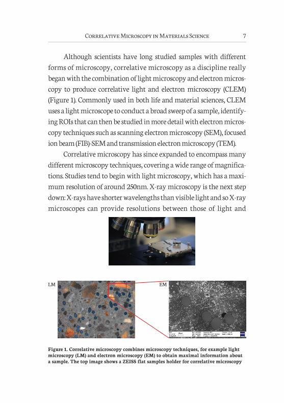
Although scientists have long studied samples with different forms of microscopy, correlative microscopy as a discipline really began with the combination of light microscopy and electron micros -copy to produce correlative light and electron microscopy (CLEM) (Figure 1). Commonly used in both life and material sci ences, CLEM uses a light microscope to conduct a broad sweep of a sample, identify-ing ROIs that can then be studied in more detail with electron micros-copy techniques such as scanning electron micros copy (SEM), focused ion beam (FIB)-SEM and transmission electron micros copy (TEM). Correlative microscopy has since expanded to encompass many different microscopy techniques, covering a wide range of magnifica-tions. Studies tend to begin with light microscopy, which has a maxi-mum resolution of around 250nm. X-ray microscopy is the next step down: X-rays have shorter wavelengths than visible light and so X-ray microscopes can provide resolutions between those of light and
LM EM
Figure 1. Correlative microscopy combines microscopy techniques, for example light microscopy (LM) and electron microscopy (EM) to obtain maximal information about a sample. The top image shows a ZEISS flat samples holder for correlative microscopy
Correlative Microscopy in Materials Science8
electron microscopes, with the latest instruments able to achieve res-olutions of up to 50nm. Furthermore, because X-rays penetrate most materials, performing X-ray microscopy on the same sample from various different angles allows researchers to build up 3D images of the sample. Known as X-ray computed tom ography (CT), this process has a lower resolution than standard X-ray microscopy, able to achieve a maximum resolution of around 3.5µm. Furthermore, the achievable resolution tends to vary with the size of the sample. TEM works by sending a beam of electrons straight through an ultra-thin sample section to a detector on the other side, with interactions between the electrons and the sample section generat-ing the image. Because electrons have very short wavelengths, TEM can produce images at atomic-scale resolutions, able to show carbon atoms in diamond, for example. SEM, on the other hand, scans an electron beam over a sample surface to generate secondary and backscattered electrons; these electrons can not only produce an image with a nanoscale resolu-tion but can also reveal other information about the sample sur-face. Secondary electrons are released when the beam interacts with weakly-bonded electrons at the sample surface, and can reveal infor mation about the topography (shape) and electrical properties of the sample. Backscattered electrons are electrons that have been reflected directly back from the sample. They tend to come from slightly deeper regions than secondary electrons and can reveal infor mation about a sample’s elemental make-up, because differ-ent atoms back scatter electrons to different extents. Although SEM has a lower resolution than TEM, it does have several advantages. For instance, because it works by scanning an electron beam over a surface, it can analyze bulk samples, rather
Correlative Microscopy in Materials Science 9
than the thin sections required for TEM, and it also has a greater depth of view. In addition to revealing information about a sample’s topol-ogy and elemental make-up, the release of secondary electrons leaves behind positively charged ‘holes’ in the inner shells of atoms at the sample surface. As these holes fill with electrons from the outer shells, the difference in energy between the two shells is released in the form of an X-ray. Because the energies of these X-rays differ for different atoms, they can be used to determine the identity of the atom, in a technique known as energy-dispersive X-ray spec-troscopy (EDS). Furthermore, the electron beam can also stimulate certain materials to emit light, in a process known as cathodo-luminescence (CL). This can reveal information on the electronic structure of a sample and is particularly useful for determining the age of geological materials. All modern SEM instruments possess the detectors required for EDS and CL. Many correlative techniques also make use of FIB-SEM, in which FIB and SEM are combined in a single system. FIB works in a similar way to SEM, but uses a beam of positively charged ions instead of negative electrons. This ion beam, which is usually pro-duced by a liquid metal ion source such as gallium, can be used both to modify a sample and to analyze it. In an FIB-SEM system, the two instruments, which can be used simultaneously, are arranged so that the focal points of the electron and ion beam coincide. At high ion doses, the FIB can dislodge atoms from the sur-face of a sample by sputtering, allowing it to modify or mill the sample. The FIB can also generate secondary electrons and ions, which can be used to produce images and provide information. For example, the secondary ions can be detected and identified by
Correlative Microscopy in Materials Science10
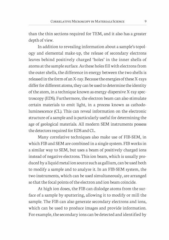
secondary ion mass spectrometry (SIMS), revealing direct infor-mation about a sample’s chemical composition. SIMS is more sen-sitive than EDS, able to detect chemical species at parts per mil-lion concentrations. Using FIB-SEM in correlative studies allows researchers to look beneath a sample’s surface. Once an ROI has been identified, the FIB can carve away successive layers of a sample while the SEM produces images of each newly uncovered surface. These images can then be combined to produce a 3D image of the ROI, in a process known as FIB-SEM tomography (Figure 2). FIB can also produce the thin sample sections required for TEM. In some specialized cases, light microscopy can also be combined with HIM, which images samples with a beam of helium ions. The lighter helium ions do not penetrate as deeply into samples as the liquid metal ions used in FIB-SEM, produc-ing secondary electrons and ions from the top 25nm of the sam-ple surface.
Figure 2. (a) Volume rendering (yellow line) of X-ray microscopy dataset (approximately 0.5mm field of view) showing transition zone defects and coarse diffusion pathways in this thermoelectric system. 200nm voxel acquisition, showing three phases (black = Mg
2Sn, medium gray = transition zone, light gray = Mg
2Si).
(b) Volume rendering of ZEISS FIB-SEM acquisition. Silicon-rich phase is depicted in orange, and the stannum-rich phase in green, with clear interdiffusion in the transition zone approximately 25–30μm wide in the center
(a) (b)
Correlative Microscopy in Materials Science 11
Able to achieve a depth of field resolution of just 0.5nm – five to ten times greater than can be achieved with FIB-SEM – HIM has proved useful for studying very thin layers of graphene, as well as the thin films used in the electronics industry. It is also indispensa-ble for studying samples containing gallium, which can be con-taminated by a FIB made up of gallium ions. ‘Low dimensional’ materials such as graphene are also some-times studied using Raman microscopy, which detects the scatter-ing of light by molecular vibrations. For example, Raman imaging has been used to study strain and disorder in graphene. Because these molecular vibrations and associated light scattering are char-acteristic for specific molecules, Raman microscopy can also be used to determine the chemical composition of samples. Correlative microscopy has already proved invaluable in two dimen sions. With ROIs often lurking below the sample surface, often a few tens of micrometers below, many researchers are now also seeking 3D insights when studying networks of structures such as pore channels in rocks, fibers in composites or cracks in alloys. This so-called correlative tomography brings together multi ple microscopy techniques able to study a 3D volume of interest, particularly X-ray microscopy and FIB-SEM tomography. Like correlative microscopy, correlative tomography provides access to a far larger range of scales for the same region than is possible with a single instrument, allowing scientists to investigate how material properties differ at different scales. Running 3D experiments over time (time-lapse) adds a fourth dimension. Such 4D experiments are particularly valuable for moni-toring changes in materials, such as following how cracks spread or spotting the moment at which metal fatigue occurs (see Case Study 2).
Correlative Microscopy in Materials Science12
IN PRACTICE Correlative microscopy has already been utilized for a wide range of scientific disciplines, from biology, zoology and palae-ontology, to materials and electronics. For example, a single team at the University of Manchester in the UK, led by Professor Philip Withers, has used correlative microscopy to study chrysalises in real time, structural changes in rats’ arteries, metal fatigue and cracking, and woven composite materials such as wind tur-bine blades. One of the great advantages of correlative microscopy is that, because it encompasses a range of different techniques, scientists can often find just the right combination for their studies. This is especially useful when studying non-biological materi als that can differ widely in composition, structure and physical properties. CLEM has proved invaluable for studying optoelectronic devices comprising different optical materials and photonic structures. For example, LEDs can be analyzed using light micros-copy and SEM. Light microscopy provides a quick overview of morphology and optical properties such as color or reflect ivity; the back scattered electrons generated by SEM can then be used to visualize contrast in cross sections, while EDS can determine ele-mental composition. The same techniques are also being used to study thin-film solar cells, which are designed to provide a low-cost alternative to silicon wafer-based cells. The structure of the interfaces between different layers in these cells can be studied at an atomic scale with scanning TEM (STEM) while EDS can provide information on elemental distribution. In addition, SEM can provide insights
Correlative Microscopy in Materials Science 13
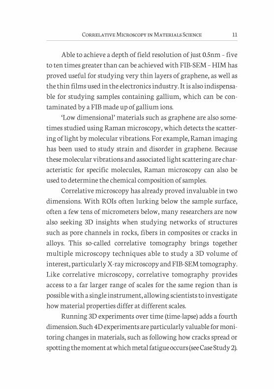
into the structural, compositional and electrical properties of the thin films, while backscattered electrons can give crystallo-graphic information. In geology, CLEM, together with CL, can be used to unearth a rock’s age and deformation history. Meanwhile, 4D correlative microscopy can reveal how rocks ‘corrode’ over time. A combination of X-ray microscopy and FIB-SEM has proved useful for studying lithium-ion batteries, as part of efforts to boost their performance and lifetime. In a study at Aalen Univer-sity in Germany, X-ray microscopy revealed bright spots below the surface of a cathode from a commercial battery (Figure 3a). During subsequent FIB-SEM analysis, the researchers collected secondary electron and backscattered images that again showed
Figure 3. (a) Overlay of SEM (gray) and X-ray microscopy (green) images. After successful correlation, the X-ray microscopy data is used as a reference for FIB-SEM navigation. (b) SEM overview of the sample. Sites of interest are highlighted by the white arrows. The inset shows a detail of site 1

Correlative Microscopy in Materials Science14
the particles (Figure 3b). EDS revealed these particles to be rich in lanthanum, rather than the expected manganese. Other teams have used correlative microscopy to study the structure of batteries, for example how they contract and expand during charging. Over many charging cycles, batteries become more damaged, so understanding this process could help to dev-elop longer-lasting products.
Correlative Microscopy in Materials Science 15
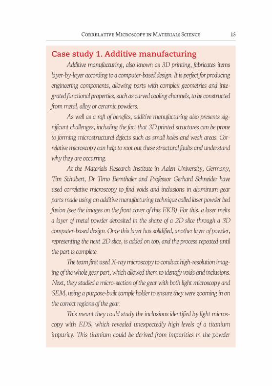
Case study 1. Additive manufacturing Additivemanufacturing,alsoknownas3Dprinting, fabricates items
layer-by-layeraccordingtoacomputer-baseddesign.Itisperfectforproducing
engineering components, allowingpartswith complexgeometries and inte-
gratedfunctionalproperties,suchascurvedcoolingchannels,tobeconstructed
frommetal,alloyorceramicpowders.
Aswellasaraftofbenefits,additivemanufacturingalsopresentssig-
nificantchallenges,includingthefactthat3Dprintedstructurescanbeprone
toformingmicrostructuraldefectssuchassmallholesandweakareas.Cor-
relativemicroscopycanhelptorootoutthesestructuralfaultsandunderstand
whytheyareoccurring.
At theMaterialsResearchInstitute inAalenUniversity,Germany,
TimSchubert,DrTimoBernthaler andProfessorGerhardSchneiderhave
used correlativemicroscopy to find voids and inclusions in aluminumgear
partsmadeusinganadditivemanufacturingtechniquecalledlaserpowderbed
fusion(seetheimagesonthefrontcoverofthisEKB).Forthis,alasermelts
a layerofmetalpowderdeposited in the shapeofa2Dslice througha3D
computer-baseddesign.Oncethislayerhassolidified,anotherlayerofpowder,
representingthenext2Dslice,isaddedontop,andtheprocessrepeateduntil
thepartiscomplete.
TheteamfirstusedX-raymicroscopytoconducthigh-resolutionimag-
ingofthewholegearpart,whichallowedthemtoidentifyvoidsandinclusions.
Next,theystudiedamicro-sectionofthegearwithbothlightmicroscopyand
SEM,usingapurpose-builtsampleholdertoensuretheywerezoominginon
thecorrectregionsofthegear.
Thismeanttheycouldstudytheinclusionsidentifiedbylightmicros-
copy with EDS, which revealed unexpectedly high levels of a titanium
impurity.This titaniumcouldbe derived from impurities in thepowder
Correlative Microscopy in Materials Science16
rawmaterial, suggestsBernthaler, or even from something as simple as
insufficientcleaning.
‘Moredigitalization (software tools)andautomationofmicroscopy
have pushed correlative technology in recent years,’ says Bernthaler. By
using‘cleversampleholders’andsoftware,workflowshavegreatlycutthe
timethatsuchinvestigationstake,headds.
WeissmayerL,SchubertT,BernthalerT,et al.Applicationsofmicroscopy
in additive manufacturing. Optik & Photonik 2015;4:44–6. (http://dx.doi.
org/10.1002/opph.201500015)
Correlative Microscopy in Materials Science 17
Case study 2. Corrosion in magnesium alloys Magnesiumalloys are lightweight, high-strength alternatives to
aluminum-basedproducts foruseincertainautomotiveandaerospace
applications.Butthesealloysaresensitivetoimpurities,whichcanpro-
motethespreadofanydamage,andarealsopronetocorrosioninhumid
orwetenvironments.Withhis teamatManchesterUniversity in the
UK,PhilipWithers,Regius Professor ofMaterials, has investigated
howcorrosiondamageoccursinthesemagnesiumalloysovertime,at
scales ranging frommillimeters tonanometersandbothatandbelow
thesurface.
Todothis,WithersandhisteamfirststudiedthealloywithX-ray
microscopywhileitwasimmersedinacorrosivesaltsolution,conducting
a single analysis every two hours. In this way,Withers and his team
producedaseriesof3Dimagesofthealloycorrodingovertime.Theythen
studiedthecorrodedalloywithSEMandcombinedthis imagewiththe
3D imagesproducedbyX-raymicroscopy inorder to identifyahighly
corrodedROIwithinthebulkofthesample.
Afteridentifyingsucharegion,theycutitoutofthealloywithFIB
to produce amicroscopic sub-sample.This required relating the detailed
surfaceimagegeneratedbySEMwiththe3DX-rayimagesinorderto
determinewheretoremovematerialfromthesurfaceinordertoreachthe
ROI.Next, they studied the sub-samplewithX-raymicroscopy, but
usinganX-raymicroscopethatcouldproduce3Dimagesatahigherlevel
ofresolution.Toincreasethemagnificationfurther,theyalsoproduceda
3DimagewithFIB-SEMtomography.Thisinvolvedremovingmultiple
layersof thesub-samplewithFIBandthen imagingeachrevealedsur-
facewithSEM,beforecombiningalltheimagestogethertoproducethe
3Dimage.
Correlative Microscopy in Materials Science18
WithX-raymicroscopy,Withersandhisteamwereabletoseepit-
tingacrossthemagnesiumalloy’ssurfacewithinseveralhoursof immer-
sion in the salt solution.After 14hours, the corrosion had spread below
the surface, as revealed by FIB-SEM. By understanding how corrosion
spreads,theresearchershopetofindawaytopreventit.
Withers and his colleagues regularly use correlativemicroscopy to
study cracks in engineeringmaterials, which relate to defects, inclusions
andother features.Thekeyistostudythesystemsin4D,saysWithers.
‘Ifyouwere tostudy lotsof samples, including fatiguedones, itwouldn’t
necessarilybethecasethatyouwouldgetthesamekindofcrackgrowth,’
explainsWithers.‘Butifyoucanstudythesamesample,wecanactually
watchhowthecracksnucleate,howtheyconnectup,andeventuallylead
tofailure.’
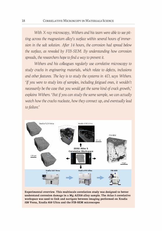
Experimental overview. This multiscale correlation study was designed to better understand corrosion damage in a Mg AZ318 alloy sample. The Atlas 5 correlative workspace was used to link and navigate between imaging performed on Xradia 520 Versa, Xradia 810 Ultra and the FIB-SEM microscopes
Correlative Microscopy in Materials Science 19
In future, he predicts that further developments in automating the
correlationbetweendifferentinstrumentsandimagingmodalitieswillbring
a‘rapidexpansion’ofmultiscalecorrelativemicroscopy.
Harris,W.Multi-scalecorrelativestudyofcorrosionevolutioninamagne-
siumalloy.ZEISSApplicationNote,December2015.
Correlative Microscopy in Materials Science20
Case study 3. Studying structures in 3D over time ‘Wefeellikekidsinacandystore.Wehaveallofthesenewtools.And
weare really able toget insideproblems thatwehaven’t beenable to solve
todate,’saysNikhileshChawla,FultonProfessorofMaterialsScienceand
EngineeringatArizonaStateUniversityintheUSA.
ChawlaisheadofthenewCenterfor4DMaterialsScience(4DMS),
fundedbyacollaborationbetweenArizonaStateUniversity,ZEISSandthe
USOfficeofNavalResearch.Thecenterwilluse correlativemicroscopy to
studystructuresin3Dovertime.
‘Theideaistoreallypushthestateoftheartin4Dmaterialscience,’
saysChawla. ‘We are essentially hoping to use these capabilities to solve
problemsinavarietyofdifferentareas,rangingfrommaterialsciencetocivil
engineering,mechanicalengineering,electricalengineeringandotherphysi-
calsciences.’
Much of Chawla’s correlative microscopy brings together X-ray
microscopyandelectronmicroscopy, includingFIB-SEM.His teamuses
ZEISSsoftwarecalledAtlas5tointegratedatafromthedifferenttechniques.
‘Atlas 5 really is revolutionary because in previous analyses finding the
sameregionintheCTandintheFIBwas like findinganeedle inahay-
stack,’hesays.
For example, his team has applied non-destructive X-ray micros-
copyandFIB-SEMto the studyof corrosion inaluminumalloys.1Using
FIBtoexposecross-sectionsofanalloysample,perpendiculartothesurface,
while simultaneously using SEM to image the cross-section face revealed
magnesium-richprecipitatesinsidethestructure.
‘Wewereabletousecompositionalinformationtodeterminethatthe
magnesiumprecipitatesareactuallydissolvingpreferentially inthecorrosive
Correlative Microscopy in Materials Science 21
fluid,’saysChawla.‘Otherkindsofprecipitatesorparticlesbasedoniron,for
example,werenotreallytouchedsothattoldusthatthemagnesium-richpre-
cipitatesarereallytheonesthatareatriskinthosekindsofalloys.’
Illustratingthediversityofhiswork,Chawla’steamisalsousingcor-
relativemicroscopytostudybeetlescalledweevils,2whichhaveverylongand
flexible‘beaks’forboringintoplants.UsingX-rayCTmicroscopyandFIB,
the researchers have revealed that the beak structure comprises alternating
hardandsoftlayers.‘Thesofttissueisakindofcomposite.It’sunique.Wecan
usetheintelligentstructuresintheweevilstodesignnew,man-madesynthetic
composites,’saysChawla.
Next, the researchers will incorporate a technique called nano-
indentation,whichemploysasharpdiamondprobetotestmechanicalprop-
erties, intotheirworkflow. ‘That isthenextavenue,tocouplethestructural
information fromCTorFIBwithmechanical property information in site.
That’ssomethingwecandoinsidetheionbeam,’heexplains.
1.SinghS,LozaJ,MerkleA,etal.Threedimensionalmicrostructuralchar-
acterization of nanoscale precipitates in AA7075-T651 by focused ion
beam (FIB) tomography. Mater Charact 2016;118:102–11. (http://dx.doi.
org/10.1016/j.matchar.2016.05.009)
2. Andrew Jansen M, Singh, S, Chawla N, et al. A multilayer micro-
mechanical model of the cuticle of Curculio longinasus Chittenden, 1927
(Coleoptera: Curculionidae). J Struct Biol 2016;195:139–58. (http://dx.doi.
org/10.1016/j.jsb.2016.05.007)
Correlative Microscopy in Materials Science22
Case study 4. Polyurethane liners in splashdown airbags Oneday,NASA’sOrioncrewmodulewillcarryastronautsbeyond
themoon,piggybackingonanewspacelaunchsystemrocket.Orion’s
first unpiloted exploration flight took place in 2014, with themodule
safelysplashingdowninthePacificOcean.Unfortunately,however,the
testrevealedafailureinOrion’screwmoduleuprightingsystem.
This system consists of five airbags that inflate upon splash-
down,keepingthemoduleuprightuntilitcanberescuedbythenavy.
Lab tests using correlativemicroscopy later revealed a problemwith
thepolyurethanelinerintheairbags,saysJamesMartinez,engineer-
ingtechnologistatNASA’sLyndonBJohnsonSpaceCenterinHou-
ston,Texas.
Thesetestssuggestedthatthepolyurethanelayerswerefusingor
binding to eachotherunderhighpressure, causing them to tear. ‘We
arechangingtoanothermaterialthathasaslipagentinsidesothatthe
twosurfacesdon’tbondtothemselvesandcanslipandslideagainsteach
otherwhenthebagisdeployed,’saysMartinez.
Whentheystudied thisnew layerwithopticalmicroscopy,how-
ever,Martinezandhisteamspottedinclusionsinthepolyurethanethin
film.Areasofbirefringenceneartheinclusionspointedtostrain.
UsingEDS,theteamdiscoveredthattheslipagentinthematerial
theyhadpurchasedisacrushedwafer-likesubstancecalleddiatomaceous
earth.Concernedthatthismightcauseabrasionwhenthepolyurethane
layers rubagainst eachother, the teamusedSEMata lowvoltage (to
prevent thematerial fromdegradingduring imaging) to look forsurface
scratchesorparticulates.TheythenusedSEMatahighvoltagetostudy
boththeinclusionsandtheslipagent.

Correlative Microscopy in Materials Science 23
‘It’s the best example of correlativemicroscopy that we have had in
sometime.Thenatureofthismaterialreallylendsitselfwelltoimagingwith
differentmodesandtechniques,’saysMartinez.NASAisnowcarryingouta
furtherseriesofsafetytests,includingonthenewliner.
Correlative Microscopy in Materials Science24
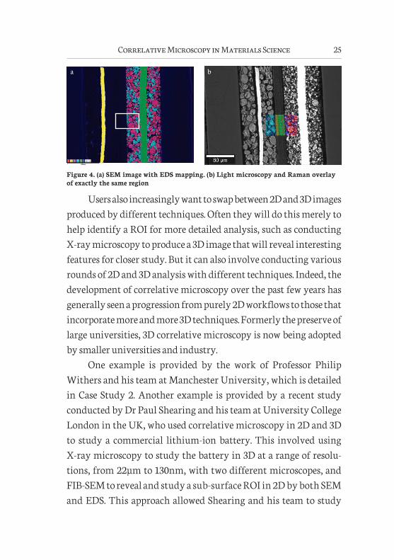
PROBLEMS AND SOLUTIONS An effective workflow is essential for getting the most out of correlative microscopy. Such a workflow defines in what order a sample will be studied by the different microscopy instruments, how ROIs on the sample will be selected and identified in different instruments, and how the resultant data will be collected, stored and processed. Usually, the level of magnification will steadily increase as the workflow progresses, in order to study a sample in progres-sively greater detail. But that’s not always the sole reason for con-ducting correlative microscopy, and these other reasons may need to be reflected in the workflow. For example, researchers may want to take advantage of the fact that different microscopy techniques can generate different information about a sample, which can be overlaid on the visual images. This is particularly the case with FIB-SEM, which can gen-erate information about the elemental composition of a sample through both EDS and SIMS. Alternatively, different microscopy techniques may be required to study the different materials in a sample, as certain materials may not respond well to specific techniques. For example, SEM works best with conducting substances such as metals, and both it and EDS can struggle with materials containing light elements such as carbon and lithium. This can clearly create problems when studying lithium-ion batteries, which employ lithium- based materials as the cathode and electrolyte, and graphite as the anode. One solution is to combine SEM with Raman microscopy (Figure 4), which can’t analyze metals but can identify light elements and organic compounds.
Correlative Microscopy in Materials Science 25
Users also increasingly want to swap between 2D and 3D images produced by different techniques. Often they will do this merely to help identify a ROI for more detailed analysis, such as conducting X-ray microscopy to produce a 3D image that will reveal interesting features for closer study. But it can also involve conducting various rounds of 2D and 3D analysis with different techniques. Indeed, the development of correlative microscopy over the past few years has generally seen a progression from purely 2D workflows to those that incorporate more and more 3D techniques. Formerly the preserve of large universities, 3D correlative microscopy is now being adopted by smaller universities and industry. One example is provided by the work of Professor Philip Withers and his team at Manchester University, which is detailed in Case Study 2. Another example is provided by a recent study conducted by Dr Paul Shearing and his team at University College London in the UK, who used correlative microscopy in 2D and 3D to study a commercial lithium-ion battery. This involved using X-ray micros copy to study the battery in 3D at a range of resolu-tions, from 22µm to 130nm, with two different microscopes, and FIB-SEM to reveal and study a sub-surface ROI in 2D by both SEM and EDS. This approach allowed Shearing and his team to study
a b
Figure 4. (a) SEM image with EDS mapping. (b) Light microscopy and Raman overlay of exactly the same region
Correlative Microscopy in Materials Science26
the battery at a range of different scales, from the whole battery to the specific ROI, revealing information on everything from the large-scale structure of the battery to the nanoscale porosity of the electrodes. This raises a critical factor that needs to be borne in mind when designing a workflow for correlative microscopy. Such workflows will often involve a combination of non-destructive techniques, such as X-ray microscopy, and destructive techniques, such as FIB-SEM, and clearly the position of any destructive tech-nique in the workflow is critical. In particular, FIB-SEM tomogra-phy, in which successive layers are removed from a ROI to build up a 3D image, obviously needs to be conducted toward the end of a workflow, as it destroys the ROI. But any treatment or modifica-tion to a sample required for a specific microscopy technique may also influence the sequence of techniques. Now, this is more of an issue when studying biological sam-ples, which are often analyzed by light microscopy with minimal treatment but need to be encased in resin or flash-frozen prior to analysis by electron microscopy. While such treatments aren’t required for non-biological samples, non-conductive materials may need to be covered in a thin layer of a metal such as platinum to improve the contrast in electron microscopy, which would influ ence the workflow. Such layers can also be applied to protect ROIs when milling them with FIB. Once an appropriate workflow has been designed, users then need an effective way to collate and combine the data produced by the different microscopy techniques. Several software tools, such as Atlas 5 from ZEISS and MAPS from FEI, will automatically collect the data from a range of different techniques; for Atlas 5, this can
Correlative Microscopy in Materials Science 27
include various forms of light microscopy, X-ray microscopy and electron microscopy. They can then produce composite images of a sample by overlaying images produced by the different techniques at different magnifications, as well as overlaying chemical infor-mation produced by techniques such as EDS and SIMS. For the software tools to be able to overlay images in this way, however, users need to match identical regions of the sample in the images produced by the different techniques. This can be done by marking the region in some way, such as by simply circling it with a pen, but this is not always desirable or possible. Alternatively, it can be done by identifying the same characteristic features in dif-ferent images, but such features can look very different at different scales. Transferring the sample between different instruments, such that it is studied at slightly different orientations, adds fur-ther difficulty, as does any treatment or modification applied to the sample. One way to make this process easier is to mount the sample on a holder that can be transferred between different microscopy instruments, thereby ensuring that the sample is always studied in the same orientation. Fiducial markers can also be added to the holder, providing fixed reference points that act as landmarks for locating the same regions and features in different images. This is what ZEISS has done with its ‘Shuttle & Find’ tech-nique, which employs a holder with three L-shaped fiducial mark-ers that can be used with many of the light and electron microscopes produced by ZEISS. By measuring the distance from these markers to features on the sample, the Shuttle & Find software module can construct a detailed co-ordinate system for accurately and automat-ically locating the same region of the sample in different images.
Correlative Microscopy in Materials Science28
This allows users to tag ROIs in images produced by a light micro-scope and then easily find those ROIs in images of the same sample produced by an electron microscope. Some manufacturers have combined light microscopy and electron microscopy in single systems, removing the need to trans-fer samples between individual instruments and making it easier to match images of the same region produced by the two tech-niques. The downside to this approach is that not only does it restrict correlative microscopy to just these two techniques, but physically combining light and electron microscopy in a single system tends to compromise their performance. It also means that the two techniques can’t be used to study different samples at the same time, reducing analytical throughput. That just leaves the challenge of storing, processing and shar-ing all the data that can now be generated by correlative micros-copy. This data is often substantial, especially if it includes 3D data sets, and thus requires lots of computer memory and processing power. Storing and processing this data in the cloud would appear to be an obvious solution, especially as it would also offer an easy way to share the data among different researchers. The problem with this approach is the great length of time it takes to upload all the data into the cloud. This data challenge is shared by many other areas of science, however, and solving it will require more than just advances in correlative microscopy.
Correlative Microscopy in Materials Science 29
WHAT’S NEXT Increased automation would help to resolve many of the cur-rent difficulties with correlative microscopy. Ideally, users would be able to study a sample on two or more instruments and then simply press a button to combine and correlate all the images, allow ing the same region to be investigated seamlessly at a broad range of different scales. Modern software tools such as Atlas 5, together with practical techniques such as Shuttle & Find, are going some way towards achieving this aim. Already, they are making it easier for research-ers to analyze materials in two, three and even four dimen sions and various different scales, and then combine the different sources of information. Nevertheless, other tools will be required to fully achieve this aim, including an automated method for revealing ROIs located within the bulk of a sample. Researchers such as those profiled in the four case studies now regularly utilize these tools and techniques in their work. This is leading to the first practical applications of correlative micro scopy, beyond purely academic research. For example, it is now being used for in-situ testing. This involves using a tech-nique like X-ray microscopy to map the pores and voids in a material such as a metal alloy and then SEM to monitor the devel opment of these pores and voids as the material is stressed until it breaks. So far, these tools and techniques mainly work with light, X-ray and electron microscopes, but similar automated approaches are required for other microscopy techniques. Especially as research ers are starting to expand correlative microscopy to encompass a broader range of techniques.
Correlative Microscopy in Materials Science30
One of these is AFM. Rather than produce a magnified optical image of a sample, AFM uses a flexible cantilever to measure the forces between the tip of the cantilever and the surface of a sample, as the tip is scanned across. Because these forces vary depending on the distance between the tip and the sample, they can be used to measure variations in the height of the surface, allowing a map of surface topology to be built up. Using the same basic approach, AFM can also probe a wide array of other material properties, inclu ding adhesion, elasticity, conductivity and temperature. AFM is often combined with light microscopy, in order to compare the topological map with a surface image and also to direct the AFM analysis. As with light and electron microscopy, the problem is matching up images produced at widely different magnifications, as AFM is able to resolve features below 1nm size. The recent development of several super-resolution microscopy techniques, which were collectively awarded the Nobel prize for chemistry in 2014, offers a novel solution to this problem. These techniques offer ways to bypass the diffraction limit that normally limits the resolution of light microscopy to 250nm, bringing their resolution closer to that of AFM. Up to now, the combination of AFM and super-resolution micro scopy has mainly been used to study biological material, because super-resolution microscopy makes use of the fluores-cent probes commonly used to illuminate cellular components in conventional fluorescence microscopy. Recently, however, a team of scientists led by Dr Cristina Flors at the Madrid Institute for Advanced Studies in Nano science in Spain used a combina-tion of AFM and a localization- based super-resolution micros-copy technique to study hybrid nanomaterials.
Correlative Microscopy in Materials Science 31
These hybrid nanomaterials comprised amyloid-like fibrils covered in the fluorescent nanocrystals known as quantum dots; such combinations of protein fibrils and nanoparticles are being developed for various applications, including as novel electrical switches and biosensors. The presence of fluorescent quantum dots on the hybrid nanomaterial made it ideal for study by super- resolution microscopy. Using the two techniques, Flors and her team were able to obtain useful information about both the struc-ture of the amyloid-like fibrils and the distribution of quantum dots over the fibrils. Super-resolution microscopy is also being combined with many other microscopy techniques, including light microscopy techniques such as fluorescence microscopy and bright-field micro scopy, as an alternative to electron microscopy. Thus scien-tists can identify interesting features on a sample with light micros copy and then zoom in for a closer look with super- resolution micro scopy. It is also being combined with electron micros copy, as both techniques have comparable resolutions. As with AFM and super-resolution microscopy, these combi-nations have so far mainly been applied to the study of biological samples, but there have been a few exceptions. For example, a combi-nation of SEM and localization- based super-resolution micros copy techniques have been used to study the structure of gold nano wires covered in fluorescent probes, as well as the activity of gold nanorods and gold nanoplates able to catalyze a reaction that produces a fluo-rescent product. For the gold nanorods, this revealed that their cata-lytic activity is higher at each end than in the middle. Similar advanced nanomaterials are also being studied by other forms of correlative microscopy. These include graphene, a
Correlative Microscopy in Materials Science32
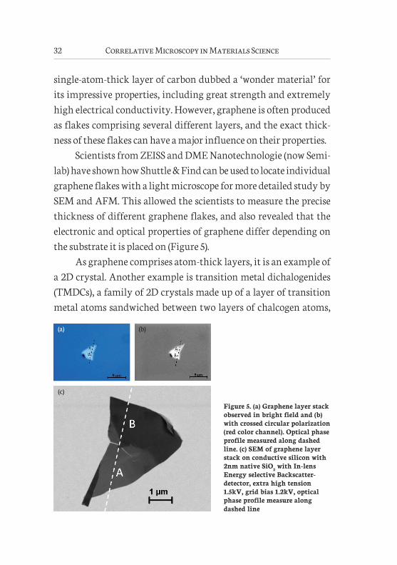
single-atom-thick layer of carbon dubbed a ‘wonder material’ for its impressive properties, including great strength and extremely high electrical conductivity. However, graphene is often produced as flakes comprising several different layers, and the exact thick-ness of these flakes can have a major influence on their properties. Scientists from ZEISS and DME Nanotechnologie (now Semi-lab) have shown how Shuttle & Find can be used to locate individual graphene flakes with a light microscope for more detailed study by SEM and AFM. This allowed the scientists to measure the precise thickness of different graphene flakes, and also revealed that the electronic and optical properties of graphene differ depending on the substrate it is placed on (Figure 5). As graphene comprises atom-thick layers, it is an example of a 2D crystal. Another example is transition metal dichalogenides (TMDCs), a family of 2D crystals made up of a layer of transition metal atoms sandwiched between two layers of chalcogen atoms,
Figure 5. (a) Graphene layer stack observed in bright field and (b) with crossed circular polarization (red color channel). Optical phase profile measured along dashed line. (c) SEM of graphene layer stack on conductive silicon with 2nm native SiO
2 with In-lens
Energy selective Backscatter- detector, extra high tension 1.5kV, grid bias 1.2kV, optical phase profile measure along dashed line
(a) (b)
(c)

Correlative Microscopy in Materials Science 33
often sulphur. Scientists at the German microscopy company WITec have shown how a similar correlative microscopy work-flow, combining light microscopy, Raman microscopy, SEM and AFM, can be used to study the TMDC tungsten disulphide (WS2). This involved using WITec’s RISE microscope, which combines Raman microscopy and SEM in a single instrument.
Correlative Microscopy in Materials Science34
FURTHER INFORMATION Bondia P, Jurado R, Casado S, etal. Hybrid nanoscopy of hybrid nanomaterials. Small 2017;13;1603784. (http://dx.doi.org/10.1002/smll.201603784) Bradley RS, Withers PJ. Correlative multiscale tomography of biological materials. MRSBulletin 2016;41(7):549–56. (https://doi.org/10.1557/mrs.2016.137) Gelb J, Finegan DP, Brett DJL, et al.Multi-scale 3D investiga-tions of a commercial 18650 Li-ion battery with correlative electron- and X-ray microscopy. J Power Sources 2017;357:77. (http://dx.doi.org/10.1016/j.jpowsour.2017.04.102) Hauser M, Wojcik M, Kim D, etal. Correlative super-resolution microscopy: New dimensions and new opportunities. ChemRev 2017. (http://dx.doi.org/10.1021/acs.chemrev.6b00604) Merkle AP, Gelb J, Orchowski A, Fuchs J. X-ray microscopy: the cornerstone for correlative characterization methods in materials research and life science. MicroscMicroanal 2014;20(Suppl 3):986. (http://dx.doi.org/10.1017/S1431927614006655) Thomas C. Correlative microscopy of optical materials. Imaging&
Microscopy Oct 13 2014. (http://www.imaging-git.com/science/electron- and-ion-microscopy/correlative-microscopy-optical-material) Valdrè G. Correlative microscopy and probing in materials sci-ence. In Rickerby DG, Valdrè G, Valdrè U, eds. Impactofelectronscanning
probemicroscopyonmaterials research. Dordrecht: Springer, 1999; 455–72. (https://link.springer.com/chapter/10.1007/978-94-011-4451-3_22) ZEISS webinar: Multi-scale correlative microscopy of energy storage and conversion devices, June 2016. (https://zeiss-microscopy.uberflip.com/h/i/242514217-multi-scale-correlative-microscopy-of-energy- storage-and-conversion-devices)

Essential Knowledge Briefings
Top Related