


Languages
Pages
Legal

ECE1371 Advanced Analog CircuitsLecture 8
COMPARATOR & FLASH ADCDESIGN
Richard [email protected]
Trevor [email protected]

8-2
alog circuita modern
peeks at
gems thatw.
ECE1371
Course Goals
• Deepen understanding of CMOS andesign through a top-down study of analog system— a delta-sigma ADC
• Develop circuit insight through brief some nifty little circuits
The circuit world is filled with many littleevery competent designer ought to kno

8-3
Homework
1: Matlab MOD1&2
2: ∆Σ Toolbox
43: Sw.-level MOD2
4
4: SC circuit
5: SC Int w/ Amp
Project
Due Friday April 10
ECE1371
Date Lecture (M 13:00-15:00) Ref
2015-01-05 RS 1 MOD1 & MOD2 ST 2, 3, A
2015-01-12 RS 2 MODN + ∆Σ Toolbox ST 4, B
2015-01-19 RS 3 Example Design: Part 1 ST 9.1, CCJM 1
2015-01-26 RS 4 Example Design: Part 2 CCJM 18
2015-02-02 TC 5 SC Circuits R 12, CCJM 1
2015-02-09 TC 6 Amplifier Design
2015-02-16 Reading Week– No Lecture
2015-02-23 TC 7 Amplifier Design
2015-03-02 RS 8 Comparator & Flash ADC CCJM 10
2015-03-09 TC 9 Noise in SC Circuits ST C
2015-03-16 RS 10 Advanced ∆Σ ST 6.6, 9.4
2015-03-23 TC 11 Matching & MM-Shaping ST 6.3-6.5, +
2015-03-30 TC 12 Pipeline and SAR ADCs CCJM 15, 17
2015-04-06 Exam Proj. Report
2015-04-13 Project Presentation

8-4
ductor
gmV
ECE1371
NLCOTD: Linear Transcon
• Useful in1 gm-C filter2 LNA3 mixer4 CT ∆Σ ADC
?V I =

8-5
day)
ircuit
ECE1371
Highlights(i.e. What you will learn to
1 Operation of Example Comparator C
2 Regeneration Time Constant τ3 Metastability, Probability of Error
4 Offset, Dynamic Offset, Auto-zeroing
5 Flash ADC
6 A Bunch of Transconductor Circuits

8-6
ratorOD2
action.
v
esholds are chosene inverters respond R/S have resolved.
set Latch:
ECE1371
Review: Latched CompaFrom Lecture #4’s 1-MHz M
• Falling phase 1 initiates regenerativeS and R connected to a Set/Reset latch
VDD
1
VSS1 1
Y+ Y–
SR
S
R
Inverter thrso that thonly after
Set/Re

8-7
Mode
is reset
n hold mode
v
set Latch:
ECE1371
Phase 1 = High: “Reset”
• Grayed-out devices are off⇒ the active part of the comparator
• R and S are low ⇒ the SR latch is i
VDD
L
VSS1 1
Y+ Y–
SR
S
R
Set/Re
L L
H HH
H

8-8
” Mode
S
R
V
Set/Reset Latch:
Time
INV2 threshold
INV2
INV1 threshold
S
R
goes high ⇒ V high
ECE1371
Phase 1 Goes Low: “LatchVDD
H
VSSL L
Y+ Y–
SR
VDD
VSS
Y+ Y–VDD
SR
INV1
R,S rise to~INV1 threshold
R,S resolve
Assume Y+ = Y– + ε:
I+δI
S
P Q
staticcurrent

8-9
s= 1V)
.4 1.6 1.8 2
input
rising transitionis poor
ECE1371
Example WaveformQuick Design in 65nm (VDD
CK
0
1
IPIN
499.5
500.5
mV
0
800
mV
0
1
0 .2 .4 .6 .8 1 1.2 1time (ns)
SR
P
Q
<1 mV

8-10
v
mission gate
Set/Reset Latch:
500
ECE1371
Better DesignVDD
1
VSS1 1
Y+ Y–
SR S
R
Use a trans
1 1
0
1
0 100 200 300 400
S
R

8-11
V in
400 500
ECE1371
Responses for Various
0
1
0
1
0
1
0 100 200 300
time (ps)
V
S
R
Vin = 10 mV, 1 mV, 0.1 mV
CK

8-12
100m 1
0 psps
ECE1371
Delay vs. V inde
lay
(ps)
1µ 10µ 100µ 1m 10mVin (V)
100
200
300
400
t d t 0 τ V inln–=
t 0 10≈τ 20≈

8-13
csr is
ks like this:
g m g mn g mp+=
m
my
Cm
ECE1371
Latch Mode Dynami• For V in near the trip point, an inverte
essentially just a transconductor:
• So near balance the comparator loo
-g
YX
-gx
C-g

8-14
is
entiallyy
cm g mv cm–=t( ) v cm 0e t– τ⁄=
ECE1371
Small-Signal Analys
• Differential component grows expon• CM component decays exponentiall
Cx g my–=Cy g mx–=
v d x y–=
v cmx y+
2--------------=
-gm
-gm
x y
C C
Cv d g mv d= Cvv d t( ) v d 0et τ/= v cm
τ Cg m--------=

8-15
DX
vcm = VDD/2
v d
ble Point
ECE1371
State-Space
• vcm → VDD/2, vd → ±VDD
VDD
VSSVSS VD
Y
Metasta

8-16
idable
andnresolved
time
out is ation of V in
ECE1371
Metastability• Metastability is fundamentally unavo
• Assuming the universe is continuousdeterministic, a comparator can be ufor any length of time
Vout
Increasing V in
At any time t, Vcontinuous func
t
8-17
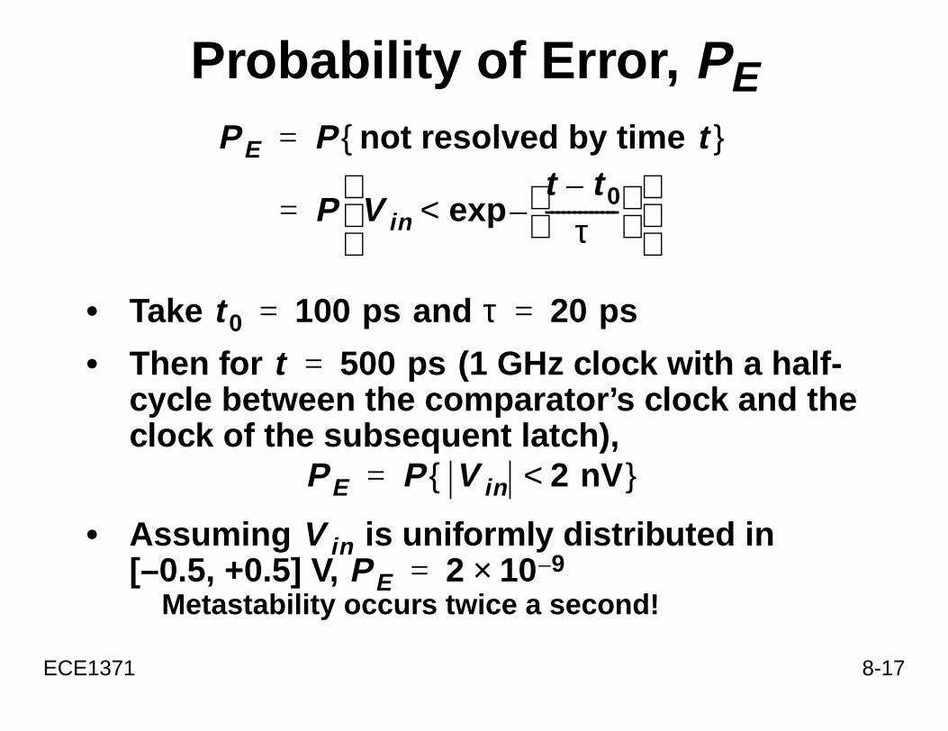
PE
ith a half-k and the
d in
t }
ECE1371
Probability of Error,
• Take and
• Then for (1 GHz clock wcycle between the comparator’s clocclock of the subsequent latch),
• Assuming is uniformly distribute[–0.5, +0.5] V,
Metastability occurs twice a second!
PE P not resolved by time{=
P V int t 0–
τ-------------
–exp<
=
t 0 100 ps= τ 20 ps=
t 500 ps=
PE P V in 2 nV<{ }=
V inPE 2 10 9–×=
8-18
ry
e enough time
ffects of
but
egradation
V in 0=
ECE1371
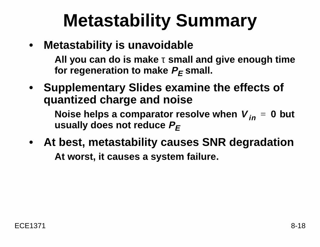
Metastability Summa• Metastability is unavoidable
All you can do is make τ small and givfor regeneration to make PE small.
• Supplementary Slides examine the equantized charge and noise
Noise helps a comparator resolve whenusually does not reduce PE
• At best, metastability causes SNR dAt worst, it causes a system failure.

8-19
ismatch inismatch in
h
ECE1371
Offset
• Obvious sources of offset include mthe input differential pair as well as mthe regenerating devices
VDD
1
VSS1 1
Y+ Y–
SR
Vt mismatc⇒ offset1 1

8-20
lso causes
Time
SR
lowly than R
ECE1371
Dynamic Offset
• Mismatched parasitic capacitance aoffset
20 mV/fF for this comparator!
• Bad design– Can fix this!
VDD
1
VSS1 1
Y+ Y–
SR C C+∆
VDD
VSS
Y+ = Y–:
S rises more s⇒ offset
1 1

8-21
or
en CK = 0
problem.
Vop
Von
ECE1371
Improved Comparat[S&T Fig. 9.36]
• Reset when CK = 1; regenerates wh• x & y don’t step if biased properly
Mismatch in overlap capacitance still a
CK
Vip Vin
x y
y
x
ckb
ckb
8-22
reamp
amp gain
from
pecially
/A
ECE1371
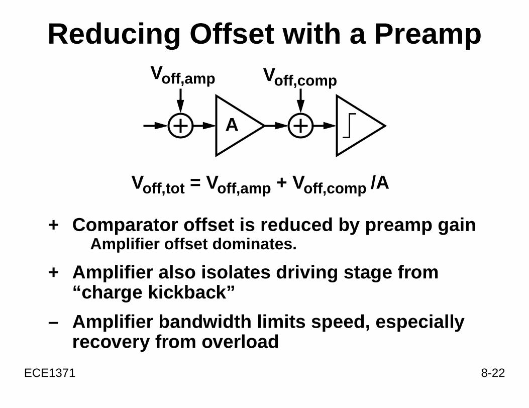
Reducing Offset with a P
+ Comparator offset is reduced by preAmplifier offset dominates.
+ Amplifier also isolates driving stage “charge kickback”
– Amplifier bandwidth limits speed, esrecovery from overload
A
Voff,amp Voff,comp
Voff,tot = Voff,amp + Voff,comp

8-23
rator
iased at its
in and Vref is
ch
1
ECE1371
Auto-zeroed SC Compa[J&M Fig 13.17]
• During P1, the inverter/amplifier is bthreshold/offset voltage
• During P2, the difference between Vamplified
Lat
P
P1
P1
P2
Vref
Vin
8-24
mp
Vout
Positiveeedback
ter to use Trackinimize dynamic
et
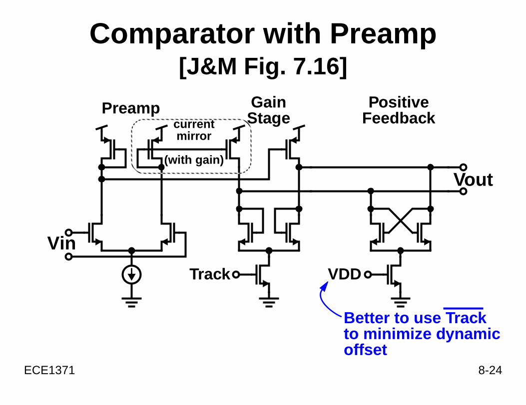
ECE1371Comparator with Prea[J&M Fig. 7.16]
Vin
Track VDD
Preamp GainFStagecurrent
mirror
Betto moffs
(with gain)
8-25
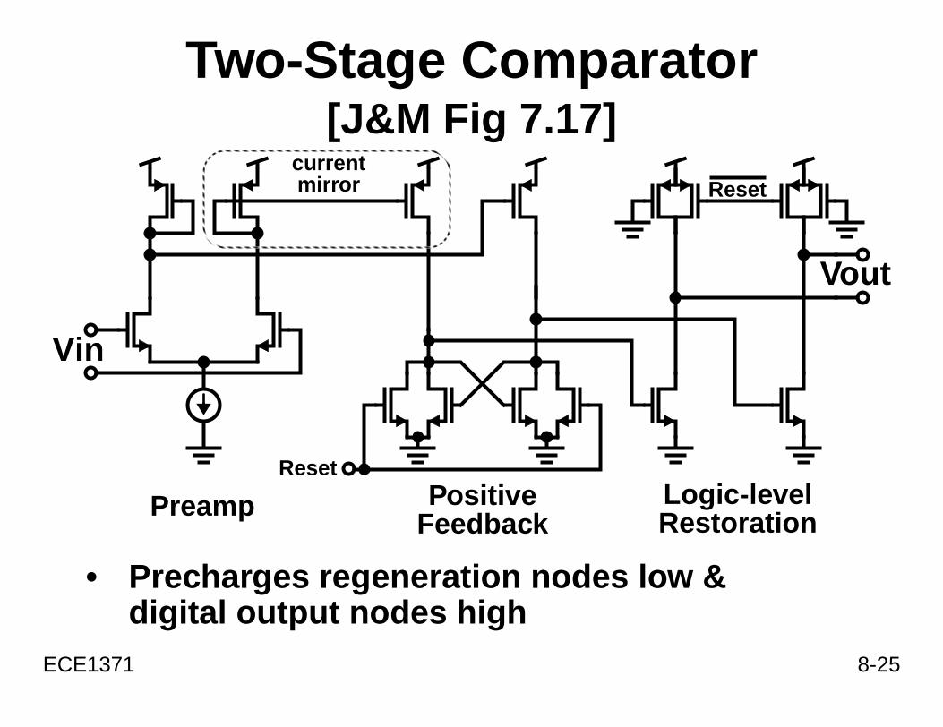
tor
&
Vout
Logic-level
Reset
Restoration
ECE1371
Two-Stage Compara[J&M Fig 7.17]
• Precharges regeneration nodes lowdigital output nodes high
Vin
Reset
Preamp PositiveFeedback
currentmirror

8-26
p
bias point
Q
Q
ECE1371
StrongArm Flip Flo
+ No static current+ Can be used as a comparator
Note that input CM voltage defines the during regeneration.
CK
CK CK
RS
R
S
D D
8-27
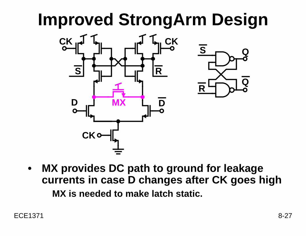
sign
eakage goes high
Q
Q
ECE1371
Improved StrongArm De
• MX provides DC path to ground for lcurrents in case D changes after CK
MX is needed to make latch static.
CK
CK CK
RS
R
S
D DMX
8-28
ent
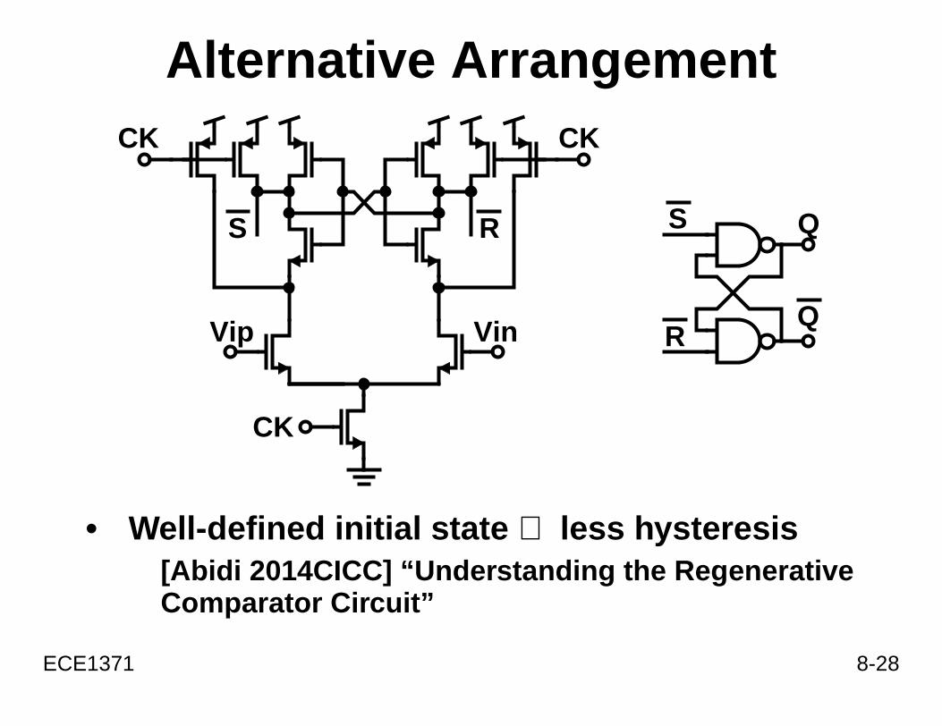
steresisegenerative
R
S Q
Q
ECE1371
Alternative Arrangem
• Well-defined initial state ⇒ less hy[Abidi 2014CICC] “Understanding the RComparator Circuit”
Vip
CK
Vin
CK CK
RS

8-29
tes
S
ECE1371
Symmetric Latch
• Faster than cross-coupled NAND ga
R
R
S
R
S
S
R
S
R
Q Q

8-30
arator
[Shibata2012].
Q
Q
Y
Y
CK
Dout
ECE1371
Yang’s High-Speed Comp
• τnom = 6 ps (!) in 65nm CMOSUsed in a CT ∆Σ ADC clocked at 4 GHz
CK
CK
YY
Vin
Y Y

8-31
rator
a>Vb
,
ECE1371
Dual-Difference Compa
Q: Where should Va– go?
Va+/–
Vb+/–High if V
Vin Vin
CK
replace: with:or
In any of our comparator circuits
Va+

8-32
Dout
ode
ECE1371
Flash ADCVin
Resistor Comparator Decode
Vref
Vref
String Bank Logic
000
001
010
111
011
H
L
H
L
H
L
L
H
L
H
Thermometercode “1-of “c
L
L
L
L
H
L

8-33
n
ber of 1s isd-Tree Adder”
logic to handl elly unlessteed to not
ECE1371
Flash Bubbles
0
0
1
0
1
1
0
0
1
0
1
0
FlashBubble
CodeViolatio
• Counting the numthe safest metho
Use a “Wallace
• Need to modifybubbles gracefububbles guaranoccur
8-34
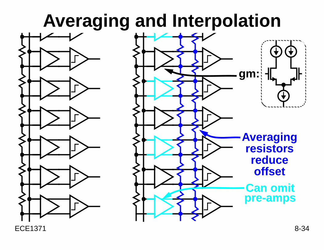
tion
Averagingresistors
Can omitpre-amps
reduceoffset
gm:
ECE1371
Averaging and Interpola

8-35
oncept
Dout
ECE1371
VCO as a Quantizer— C
+ Simple
+ Monotonic
– Not linear
– Ill-defined full-scale
CounterReset
Latch
CK
VinVCO

8-36
cillator
to current
ECE1371
Current-Controlled Ring Os(CCRO)
• Oscillation frequency is proportional
⇒ Can make a fairly linear quantizer
Iin
8-37
OR = Q!
DQ
DQ
DQ
DQ
its
ECE1371
CCRO + Phase latch + EXIin
DQ
DQ
DQ
DQ
DQ
DQ
CK
Sum of Changed B
EXOR
Dout

8-38
uantizere 2 nd FF
l-scale.
rrangementke mid-scale
olation tofosc ceiling
th the EXORh-shaping
ECE1371
Improvements to CCRO Q• Put EXOR before 1 st FF and remov
To eliminate unnecessary delay.
• Add inverters to increase resolutionMust keep fosc constant to maintain ful
• Use 2 rings in a pseudo-differential aTo cancel even-order distortion and maself-referenced.
• Use multiple rings with phase interpincrease resolution without hitting
• Driving the elements of the DACs wioutputs directly results in mismatc
8-39
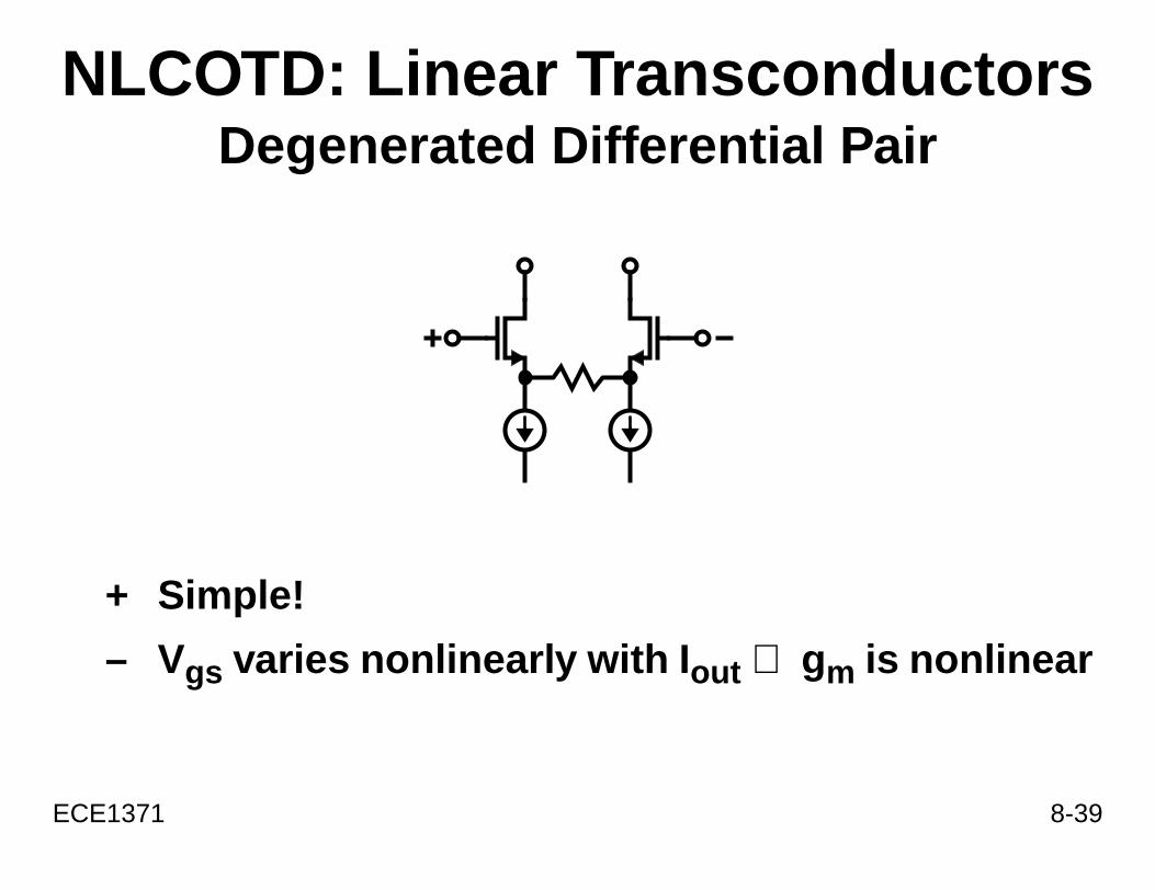
ductorsPair
gm is nonlinear
ECE1371
NLCOTD: Linear TransconDegenerated Differential
+ Simple!
– Vgs varies nonlinearly with I out ⇒

8-40
gs
r linearity
ECE1371
Force Constant V
• Id constant ⇒ Vgs constant
– Linearity dependent on current-mirro
Id

8-41
scodes and into output
b
ECE1371
Cascomp
• Vgs of input devices replicated in cadistortion-cancelling current injected
+ All NMOS ⇒ fast
– Cancellation depends on matchingShould tie bulk to source?
Vb V
V1
V1 V2
V2R
R’

8-42
and BW
t swing
uperOS”
ECE1371
Add Op Amps
+ Linearity limited only by op amp gain
+ High output resistance
– Output compliance depends on inpu
“sM

8-43
ent
at
gs
ECE1371
Mirror the Output Curr
+ Output compliance is VDD – 2 V ds
– Top of differential pair at VDD – V

8-44
nt
air
Vb2
ECE1371
Fold the Output Curre
+ Increased headroom for differential p
+ Increased output resistance
Vb1
Vb2

8-45
t8]
creates a
n the
gm1 gm2
gm
Vin
Vin
ECE1371
Multi-Tanh Double[Gilbert JSSC Dec. 199
• With BJTs, ratioing the emitter areaswell-controlled offset
• With the right offset, the cubic term inonlinearity is zero!
n 1 n1
Vin
n 2 3+ 3.73 15 4⁄≈= =

8-46
an ang with W/L
ECE1371
MOS Quad
• Supposedly can get less distortion thdegenerated differential pair by fiddli

8-47
dayircuit
ECE1371
What You Learned To1 Operation of Example Comparator C
2 Regeneration Time Constant τ3 Metastability, Probability of Error
4 Offset, Dynamic Offset, Auto-zeroing
5 Flash ADC
6 A Bunch of Transconductor Circuits

8-48
sy)
ECE1371
Supplementary Slide(Regarding Metastabilit
8-49
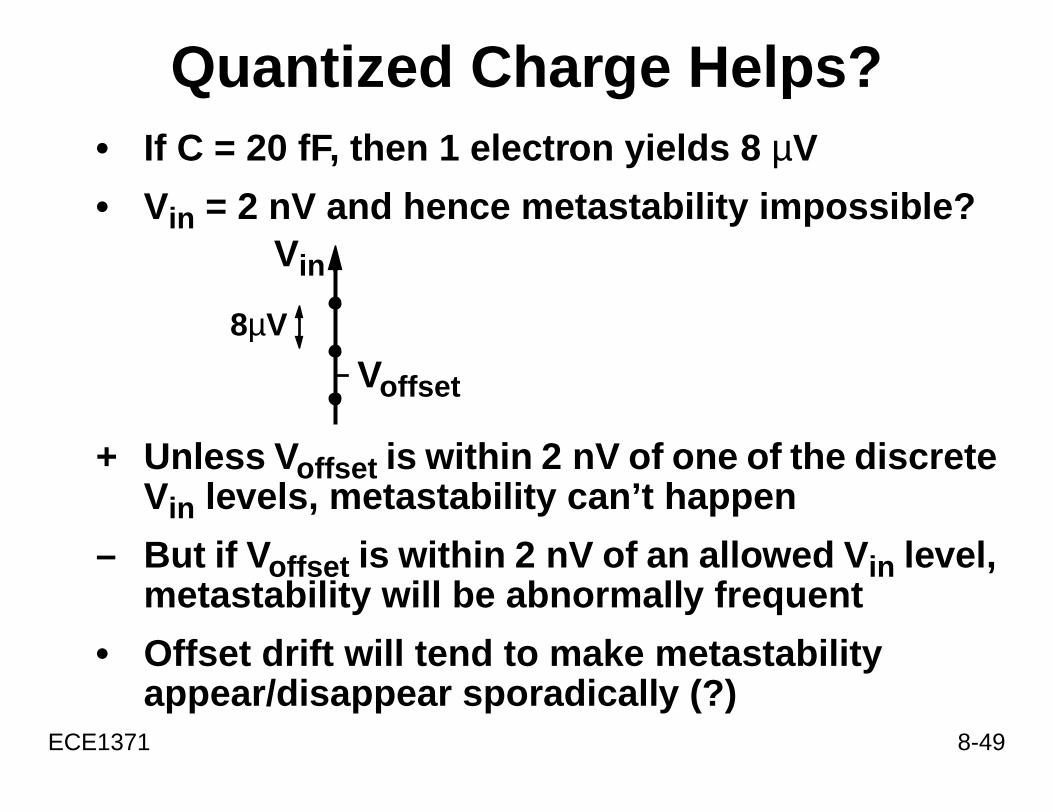
lps?µV
mpossible?
f the discreten
wed V in level,uent
bility
ECE1371
Quantized Charge He• If C = 20 fF, then 1 electron yields 8
• Vin = 2 nV and hence metastability i
+ Unless V offset is within 2 nV of one oVin levels, metastability can’t happe
– But if V offset is within 2 nV of an allometastability will be abnormally freq
• Offset drift will tend to make metastaappear/disappear sporadically (?)
Vin
8µV
Voffset

8-50
guaranteein = 0
ve if it is
alhich results
ditions thatot reduce
ECE1371
Noise Helps?• kT/C = 500 µV, so it is impossible to
that metastability will result even if V
+ Noise does help a comparator resolmetastable
– But for any given noise (random initicondition), there is always an input win metastability
• Noise makes it hard to set initial conwill result in metastability, but does nthe probability of error

8-51
ring
tability?
3)kT g m
ECE1371
What About Noise DuRegeneration?
• Noise from the g ms prevents metas
-gm
-gm
x y
C C
S 8 3⁄( )kT g m= S 8 ⁄(=
8-52
Noise
ct of the
S h t( ) 2 td∞–
∞
∫=
ECE1371
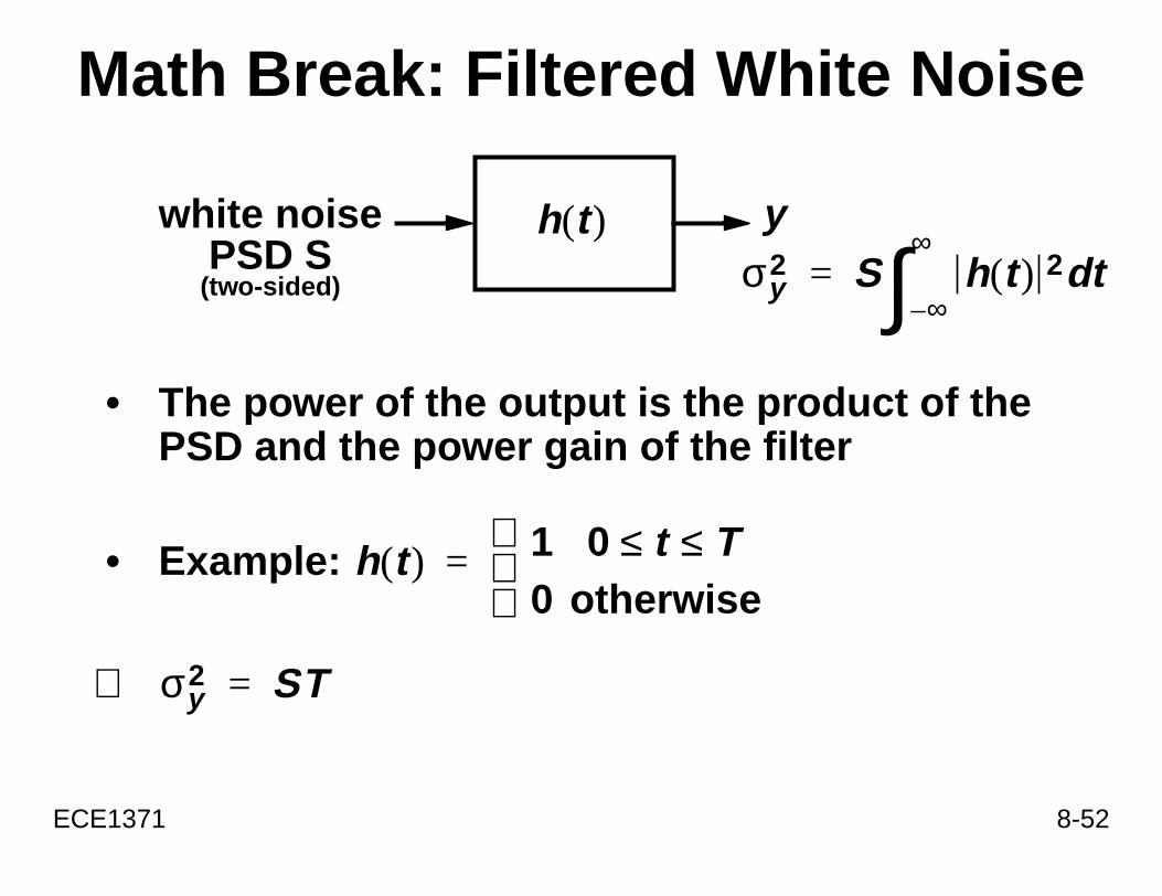
Math Break: Filtered White
• The power of the output is the produPSD and the power gain of the filter
• Example:
⇒
h t( )white noisePSD S
yσy
2(two-sided)
h t( ) 1 0 t T≤ ≤0 otherwise
=
σy2 ST=

8-53
:se
h time
”the changeant variance
t
S2C2-----------t
t
nt
ECE1371
Circuits ApplicationIntegrated White Noi
• Variance of V increases linearly wit
• “Random Walk” or “Brownian MotionFor any given increment of time , in V is a random variable with const
⇒
t = 0S A2/Hz
(one-sided PSD)
C F V(t)
σv2 =
∆
δ t( ) V t( ) V t ∆t–( )–≡ σδ2 consta=

8-54
t T≤rwise
y
ECE1371
Today’s Application
h t( ) et τ/ 0 ≤0 othe
=
white noisePSD S
(one-sided) T0t
σy2 Sτ
4------ e
2Tτ
--------1–
=
h t( )

8-55
f a Sum
ent randomctions
volution of
z x– ) xd
ECE1371
Another Math Fact: PDF o
• Suppose x and y are two independvariables with probability density fun(PDFs) and
• Then the PDF of their sum is the conthe individual PDFs
⇒
ρx x( ) ρy y( )
z x y+= ρz z( ) ρx x( )ρy (∞–
∞
∫=

8-56
tability?
3)kT g m
ECE1371
Back to Circuits
• Noise from the g ms prevents metas
-gm
-gm
x y
C C
S 8 3⁄( )kT g m= S 8 ⁄(=
8-57
kT g m
ξd
. with varianceSii τ4C2----------- e
2tτ
------1–
=
B: Convolution washes outdiscreteness in v 0’s PDF
ECE1371
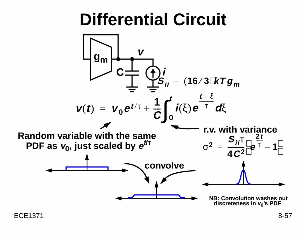
Differential Circuit
gmv
CSii 16 3⁄( )=
v t( ) v 0et τ/ 1C---- i ξ( )e
t ξ–τ
-----------
0
t
∫+=
i
r.vRandom variable with the same
PDF as v0, just scaled by et/τ σ2
convolve
N

8-58
400 ps
mV, in
50 kV
n the inputegligibleof the initial
ECE1371
Making Numbers…• Assume g m = 1 mA/V, C = 20 fF, t =
⇒ τ = 20 ps; 20 τ to resolve
• If v0 uniformly distributed in [–2,+2]then 1 st term is uniformly distributed[–1,+1] MV
• Standard deviation of 2 nd term is 2Equivalent to a 0.5-mV initial condition
• Noise during regeneration helps wheis known to be small, but is usually ncompared to the exponential growthconditions
Top Related