


Languages
Pages
Legal

cchhiippKKIITT™™ UUnnoo3322™™ BBooaarrdd RReeffeerreennccee MMaannuuaall Revision: July 21, 2011 1300 NE Henley Court, Suite 3
Pullman, WA 99163 (509) 334 6306 Voice | (509) 334 6300 Fax
Doc: 502-209 page 1 of 17
Copyright Digilent, Inc. All rights reserved. Other product and company names mentioned may be trademarks of their respective owners.
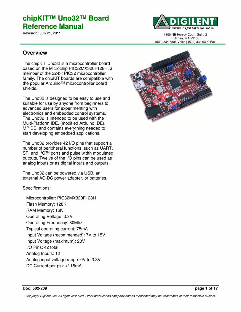
Overview The chipKIT Uno32 is a microcontroller board based on the Microchip PIC32MX320F128H, a member of the 32-bit PIC32 microcontroller family. The chipKIT boards are compatible with the popular Arduino™ microcontroller board shields. The Uno32 is designed to be easy to use and suitable for use by anyone from beginners to advanced users for experimenting with electronics and embedded control systems. The Uno32 is intended to be used with the Multi-Platform IDE, (modified Arduino IDE), MPIDE, and contains everything needed to start developing embedded applications. The Uno32 provides 42 I/O pins that support a number of peripheral functions, such as UART, SPI and I2C™ ports and pulse width modulated outputs. Twelve of the I/O pins can be used as analog inputs or as digital inputs and outputs. The Uno32 can be powered via USB, an external AC-DC power adapter, or batteries. Specifications:
Microcontroller: PIC32MX320F128H
Flash Memory: 128K
RAM Memory: 16K
Operating Voltage: 3.3V
Operating Frequency: 80Mhz
Typical operating current: 75mA
Input Voltage (recommended): 7V to 15V
Input Voltage (maximum): 20V
I/O Pins: 42 total
Analog Inputs: 12
Analog input voltage range: 0V to 3.3V
DC Current per pin: +/-18mA
chipKIT Uno32 Reference Manual
www.digilentinc.com page 2 of 17
Copyright Digilent, Inc. All rights reserved. Other product and company names mentioned may be trademarks of their respective owners.
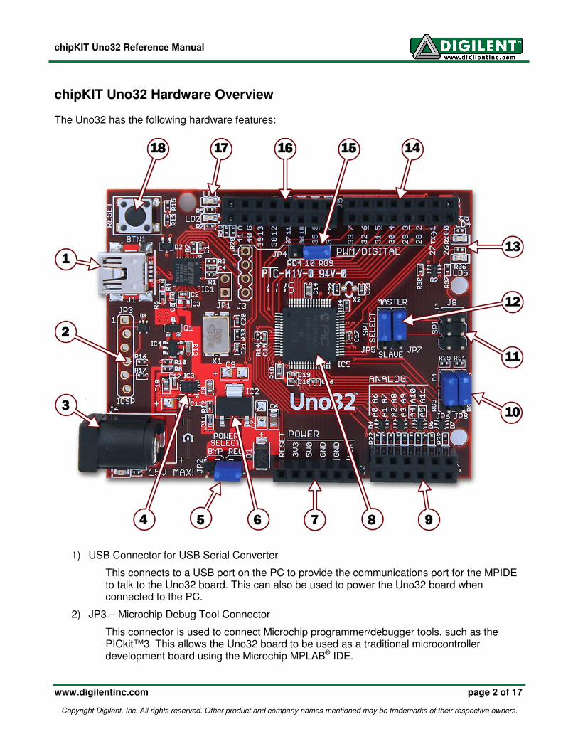
chipKIT Uno32 Hardware Overview The Uno32 has the following hardware features:
1) USB Connector for USB Serial Converter
This connects to a USB port on the PC to provide the communications port for the MPIDE to talk to the Uno32 board. This can also be used to power the Uno32 board when connected to the PC.
2) JP3 – Microchip Debug Tool Connector
This connector is used to connect Microchip programmer/debugger tools, such as the PICkit™3. This allows the Uno32 board to be used as a traditional microcontroller development board using the Microchip MPLAB® IDE.
chipKIT Uno32 Reference Manual
www.digilentinc.com page 3 of 17
Copyright Digilent, Inc. All rights reserved. Other product and company names mentioned may be trademarks of their respective owners.
3) J4 – External Power Connector
This is used to power the Uno32 board from an external power supply. This is a 5.5mm x 2.1mm barrel connector. It is wired with the center terminal as the positive supply voltage. The power supply voltage must be in the range 7V to 15V.
4) Power Supply – 3.3V regulator
Voltage regulator for the 3.3V power supply. This power supply can provide up to 500mA of current.
5) JP2 – Power Select Jumper
This jumper is used to route power from the external power connector through the on-board 5V voltage regulator or to bypass the 5V regulator. The REG position routes power through the 5V regulator. The BYP position bypasses the on-board 5V regulator. With this jumper in the BYP position the maximum input voltage that can be applied at the external power connector is 6V.
6) Power Supply – 5V regulator
On-Board 5V voltage regulator. This regulates the input voltage applied at the external power connector to 5V. This is used to power the 3.3V regulator and to provide 5V power to shields. This regulator can provide up to 800mA of current.
7) J2 – Shield Power Connector
This connector provides power to I/O expansion shields connected to the board.
8) PIC32 Microcontroller
This is the PIC32MX320F128H microcontroller that is the main processor for the board.
9) J7 – Analog Signal Connector
This connector provides access to analog/digital I/O pins on the microcontroller.
10) JP6/JP7 – A4/A5 Signal Select Jumpers
These jumpers are used to switch pins 9 & 11 on connector J7 between analog inputs A4 and A5 or the I2C signals SDA and SCL
11) J8 – SPI Signal Connector
This connector provides alternative access to the SPI signals. This is used by some shields for access to the SPI bus.
12) JP5/JP7 – SPI Master/Slave Select Jumpers
These jumpers are used to switch the SPI signals for use of the Uno32 board as an SPI master device or as an SPI slave device. Both jumpers should be switched together. Place the shorting blocks in the MASTER position for master operation and in the SLAVE position for slave operation. Normally, these jumpers are in the MASTER position.
13) User LEDs
Two LEDs connected to digital signal pins 13 and 43.
14) J6 – Digital Signal Connector
This connector provides access to digital I/O pins on the microcontroller.
15) JP4 – Pin 10 Signal Select Jumper
chipKIT Uno32 Reference Manual
www.digilentinc.com page 4 of 17
Copyright Digilent, Inc. All rights reserved. Other product and company names mentioned may be trademarks of their respective owners.
This jumper is used to switch connector J5 pin 5 (digital signal 10) between pulse width modulator (PWM) operation and SPI operation. The jumper is placed in the RD4 position for PWM output and in the RG9 position for SPI operation.
16) J5 – Digital Signal Connector
This connector provides access to digital I/O pins on the microcontroller.
17) Communications Status LEDs
These LEDs indicate activity on the USB serial interface.
18) Reset Button
This button can be used to reset the microcontroller, restarting operation from the boot loader.
chipKIT Uno32 Reference Manual
www.digilentinc.com page 5 of 17
Copyright Digilent, Inc. All rights reserved. Other product and company names mentioned may be trademarks of their respective owners.
chipKIT Uno32 Jumper Settings The chipKIT™ Development Platforms use a Microchip PIC32 Microcontroller. These are 32-bit products that bring unprecedented features to the Arduino™ community. In order to maintain compatibility with existing hardware/software while maintaining user accessibility to these advanced features, additional jumpers and row headers are provided. This document describes the functionality of the jumpers listed in figure 1.
Figure 1: chipKIT™ UNO32 Jumpers
Jumper Function JP2 POWER SELECT: Used to connect/bypass on-board 5V regulator when using an
external power supply connected to J4
J4 supply is regulated (i.e. 5V will be
present on 5V pin) J4 supply bypasses regulator (i.e.
Supply voltage will be present on 5V pin)
Note: A 3.3V on-board regulator will always be enable regardless of JP2 settings to protect the PIC32 MCU Not sure what this does? Play it safe and keep JP2 on the two right-most pins. (i.e. J4 supply is regulated)
JP4 PWM/DIGITAL SELECT: Configures pin 10 on J5 to be used as a PWM output or a Digital Input/Output.
Pin 10 configured as a Digital
Input/Output Pin 10 configured as a PWM output
chipKIT Uno32 Reference Manual
www.digilentinc.com page 6 of 17
Copyright Digilent, Inc. All rights reserved. Other product and company names mentioned may be trademarks of their respective owners.
JP5/JP7 SPI SELECT: Used to configure the chipKIT™ as either a Master or Slave when using the SPI (Serial Peripheral Interface). The chipKIT™ board can be connected to another device or even another chipKIT™ through the SPI connector (J8).
chipKIT™ configured as a SPI Master
chipKIT™ configured as a SPI Slave For more information on SPI, please visit Wikipedia’s SPI page at: http://en.wikipedia.org/wiki/Serial_Peripheral_Interface_Bus#Mode_Numbers
JP6/JP8 I2C/ANALOG PIN SELECT: Used to configure A4 and A5 for functionality as an Analog input or to be used as I2C communication pins.
A4 and A5 on J7 are configured to
be used as analog inputs A4 and A5 are configured to be used as
I2C communication lines (A4 – SDA, A5 – SCL )
For more information on I2C, please visit Wikipedia’s I2C page at:
http://en.wikipedia.org/wiki/I2C

chipKIT Uno32 Reference Manual
www.digilentinc.com page 7 of 17
Copyright Digilent, Inc. All rights reserved. Other product and company names mentioned may be trademarks of their respective owners.
chipKIT Uno32 Hardware Description
MPIDE and USB Serial Communications The Uno32 board is designed to be used with the Multi-Platform IDE (MPIDE). The MPIDE development platform was produced by modifying the Arduino™ IDE and is fully backward compatible with the Arduino IDE. The MPIDE uses a serial communications port to communicate with a boot loader running in the Uno32 board. The serial port on the Uno32 board is implemented using an FTDI FT232R USB serial converter. Before attempting to use the MPIDE to communicate with the Uno32, the appropriate USB device driver must be installed. The Uno32 board uses a standard mini-USB connector for connection to a USB port on the PC. When the MPIDE needs to communicate with the Uno32 board, the board is reset and starts running the boot loader. The MPIDE then establishes communications with the boot loader and downloads the program to the board. When the MPIDE opens the serial communications connection on the PC, the DTR pin on the FT232R chip is driven low. This pin is coupled through a capacitor to the MCLR pin on the PIC32 microcontroller. Driving the MCLR line low resets the microcontroller, restarting execution with the boot loader. This automatic reset action when the serial communications connection is opened can be disabled. To disable this operation, there is a cut-able trace on the bottom of the board between the pins of JP1. JP1 is normally not loaded. If the trace between the pins on JP1 has been cut, the automatic reset operation can be restored by loading JP1 and inserting a shorting block across it.
Two red LEDs (LD1 and LD2) will blink when data is being sent or received between the Uno32 and the PC over the serial connection. The header connector J3 provides access to the other serial handshaking signals provided by the FT232R. Connector J3 is not loaded at the factory and can be installed by the user to access these signals.
Power Supply The Uno32 is designed to be powered either from USB or from an external power supply. There is an automatic switchover circuit that causes the external supply to be used if both supplies are present. The power supply section in the Uno32 uses two voltage regulators. The first regulates the external voltage to 5V to power the VCC5V0 bus. The second regulates the VCC5V0 bus to 3.3V to provide power to the VCC3V3 bus that powers the PIC32 microcontroller. The 5V voltage regulator is normally an NCP1117. The board is designed to be able to also use an LM1117, but the NCP1117 is the part normally used. The NCP1117 is rated for an output current of 1A (the LM1117 is rated for 800mA). The dropout voltage of the NCP1117 is a maximum of 1.2V at the rated output current (1.3V for the LM1117). There is a reverse polarity protection diode in the external power supply circuit. Considering the diode drop plus the forward drop across the regulator, the minimum input voltage to the regulator should be 7V to produce a reliable 5V output. The absolute maximum input voltage of both the NCP1117 and the LM1117 is 20V. The recommended maximum operating voltage is 15V. For input voltages above 9V, the regulator will get extremely hot when drawing high currents. Both the NCP1117 and the LM1117 have output short circuit protection and internal thermal protection and will shut down automatically to prevent damage.
chipKIT Uno32 Reference Manual
www.digilentinc.com page 8 of 17
Copyright Digilent, Inc. All rights reserved. Other product and company names mentioned may be trademarks of their respective owners.
The 3.3V regulator is a Microchip MCP1725. This regulator is rated for a maximum output current of 500mA. The absolute maximum input voltage for the MCP1725 is 6V. This regulator has internal short circuit protection and thermal protection. It will get noticeably warm when the current consumed by the VCC3V3 bus is close to the 500mA maximum. The 5V power bus, VCC5V0 can be powered from one of three sources: 1) The USB5V0 bus when the board is operating under USB power; 2) The output of the on-board 5V regulator when operating from an external 7V – 15V supply; or 3) Directly from the external supply when operating from a regulated 5V external supply and jumper JP2 is in the BYP position. Switchover from USB power to external power is done automatically and the external supply will be used if both are present. Jumper JP2 is used to route the external power supply voltage through the on-board 5V regulator or directly to the VCC5V0 bus, bypassing the on-board 5V regulator. Normally, JP2 should be in the REG position. This routes the external supply through the 5V regulator. Operation from an externally regulated 5V supply is provided by placing the jumper in the BYP position. The forward drop across the MCP1725 is typically 210mV (350mV max) at 500mA output. With JP2 in the BYP position, this will allow correct operation of the 3.3V power supply from an input voltage down to 3.5V. This allows powering the board from batteries and other lower voltage power sources. In this case, the VCC5V0 power bus will not be powered at 5V. NOTE: It is extremely important to observe the MCP1725 maximum input voltage rating of 6V when JP2 is in the BYP position. Applying more than 6V to the external power input with the jumper in the BYP position can destroy the 3.3V regulator and possibly the PIC32 microcontroller as well.
The PIC32 microcontroller is rated to use a maximum of 75mA of current when operating at 80Mhz. This allows up to 425mA from the VCC3V3 bus and up to 925mA from the VCC5V0 bus to power external devices. The POWER connector, J2, is used to provide power to shields connected to the Uno32 board. The following pins are provided on this connector:
P32_RST (pin 1): This connects to the MCLR pin on the PIC32 microcontroller and can be used to reset the PIC32.
VCC3V3 (pin 2): This routes the 3.3V power bus to shields. This pin can provide ~425mA.
VCC5V0 (pin 3): This routes the 5V power bus to shields. This pin can provide up to ~900mA to shields, however to total provided by pins 2 and 3 shouldn’t exceed 925mA.
GND (pin 4, 5): This provides a common ground connection between the Uno32 and the shields.
VIN (pin 6): This connects to the voltage provided at the external power supply connector. This can be used to provide unregulated input power to the shield. It can also be used to power the Uno32 board from the shield instead of from the external power connector.
5V Compatibility The PIC32 microcontroller operates at 3.3V. The original Arduino boards operate at 5V, and many Arduino shields are designed to operate at 5V. There are two issues to consider when dealing with 5V compatibility for 3.3V logic. The first is protection of 3.3V inputs from damage caused by 5V signals. The second is whether the 3.3V output is high enough to be recognized as a logic high value by a 5V input. The digital I/O pins on the PIC32 microcontroller are 5V tolerant. The analog capable I/O pins are not 5V tolerant. To
chipKIT Uno32 Reference Manual
www.digilentinc.com page 9 of 17
Copyright Digilent, Inc. All rights reserved. Other product and company names mentioned may be trademarks of their respective owners.
provide 5V tolerance on those pins, the Uno32 contains clamp diodes and current limiting resistors to protect them from 5V input voltages. The fact that all I/O pins are 5V tolerant means that it is safe to apply 5V logic levels to any pins on the board without risk of damaging the PIC32 microcontroller. The minimum output high voltage of the PIC32 microcontroller is rated at 2.4V when sourcing 12mA of current. When driving a high impedance input (typical of CMOS logic) the output high voltage will be close to 3.3V. Some 5V devices will recognize this voltage as a logic high input, and some won’t. Many 5V logic devices will work reliably with 3.3V inputs.
Input/Output Connections The Uno32 board provides 42 of the I/O pins from the PIC32 microcontroller to pins on the input/output connectors, J5, J6, and J7. The PIC32 microcontroller can source or sink a maximum of 18mA on all digital I/O pins. However, to keep the output voltage within the specified voltage range (VOL 0.4V, VOH 2.4V) the pin current must be restricted to +7/-12mA. The maximum current that can be sourced or sunk across all I/O pins simultaneously is +/-200mA. The maximum voltage that can be applied to any I/O pin is 5.5V. For more detailed specifications, refer to the PIC32MX3XX/4XX Data Sheet available from the Microchip web site. Connectors J5 and J6 are 2x8 female pin header connectors that provide digital I/O signals. The outer row (closer to the board edge) of pins on these connectors corresponds to the I/O connector pins on an Arduino Uno or Duemilanove board. The inner row of pins provides access to the extra I/O signals provided by the PIC32 microcontroller. Connector J7 is a 2x6 female pin header connector that provides access to the analog input pins on the microcontroller. The outer row
of pins corresponds to the six analog pins on an Arduino Uno or Duemilanove. The inner row of pins are the additional I/O signals provided by the PIC32 microcontroller. The analog pins on J7 can also be used as digital I/O pins. The chipKIT/Arduino system uses logical pin numbers to identify digital I/O pins on the connectors. The logical pin numbers for the I/O pins on the Uno32 are 0 – 43. These pin numbers are labeled in the silk screen on the board. Pin numbers 0 – 13 are the outer row of pins on J6 and J5, going from right to left. Pin numbers 14 – 19 are the outer row of pins on J7 going left to right. Pins 20 – 25 are the inner row of pins on J7 going left to right. Pin numbers 26 – 41 are the inner row of pins on J6 and J5 going right to left. Pin 42 is the pin labeled A on J5. This pin is normally the reference voltage for the microcontroller’s A/D converter, but can also be used as a digital I/O pin. In addition to the connector pin, Pin 13 also connects to the user LED LD4. Pin 43 connects to user LED LD5. Pin 43 pin does not go to any connector. The analog inputs on connector J7 are assigned pin numbers. The outer row of pins on J7 are analog inputs A0 – A5. The inner row of pins are A6 – A11. These pins are also assigned digital pin numbers: A0 – A5 are digital pins 14 – 19, and A6 – A11 are 20 – 25..
Peripheral I/O Functions The PIC32 microcontroller on the Uno32 board provides a number of peripheral functions. The following peripherals are provided: UART port 1: Asynchronous serial port. Pin 0 (RX), Pin 1 (TX). These pins are connected to I/O connector J6 and are also connected to the FT232R USB serial converter. It is possible to use these pins to connect to an external serial device when not using the USB serial
chipKIT Uno32 Reference Manual
www.digilentinc.com page 10 of 17
Copyright Digilent, Inc. All rights reserved. Other product and company names mentioned may be trademarks of their respective owners.
interface. This uses UART1 (U1RX, U1TX) on the PIC32 microcontroller. UART port 2: Asynchronous serial port. Pin 39 (RX), Pin 40 (TX). This uses UART2 (U2RX, U2TX) on the PIC32 microcontroller. SPI: Synchronous serial port. Pin 10 (SS), Pin 11 (MOSI), Pin 12 (MISO), Pin 13 (SCK). These signals also appear on connector J8. Jumpers JP5 and JP7 are used to select whether the Uno32 operates as a Master (transmit on MOSI, receive on MISO) or a Slave (transmit on MISO, receive on MOSI) device. The shorting blocks on JP5 and JP7 are normally placed in the Master position for the Uno32 to function as an SPI master. Additionally, jumper JP4 is used to select PWM output or the SPI SS function on pin 10. The jumper on JP4 should be in the RD4 position to select PWM output. It should be in the RG9 position to select the SPI SS function. This uses SPI2 (SS2, SDI2, SDO2, SCK2) on the PIC32 microcontroller. I2C: Synchronous serial interface. The PIC32 microcontroller shares analog pins A4 and A5 with the two I2C signals SDA and SCL. Jumpers JP6 and JP8 are used to select whether the analog pin functions or the I2C pin functions are being used. The shorting blocks are placed in the A4/A5 position to select the analog input function or general digital I/O. They are placed in the RG3/RG2 position to use the pins for I2C operation. This uses I2C1 (SDA1, SCL1) on the PIC32 microcontroller. Note: The I2C bus uses open collector drivers to allow multiple devices to drive the bus signals. This means that pull-up resistors must be provided to supply the logic high state for the signals. These pull-up resistors are not on the Uno32 board and must be provided externally. The resistance of the pull-up resistor to use depends on the total number of devices on the bus, the length of wire, and the clock speed being used. It essentially depends on distributed capacitance on the bus. The higher the distributed capacitance and the faster the clock speed, the smaller the
resistance should be. Values typically used are in the range of 2K to 10K ohms. PWM: Pulse width modulated output. Pins 3 (OC1), 5 (OC2), 6 (OC3), 9 (OC4), and 10 (OC5). External Interrupts: Pin 38 (INT0), Pin 2 (INT1), Pin 7 (INT2), Pin 8 (INT3), Pin 35 (INT4) User LEDs: Pin 13 (LD4), Pin 43 (LD5). Pin 13 is shared between a connector pin and the LED. Pin 43 only goes to the LED and not any connector pin. Driving the pin high turns the LED on, driving it low turns it off. A/D Converter Reference: Labeled A, the left-most outer pin on connector J5. This is used to provide an external voltage reference to determine the input voltage range of the analog pins. The maximum voltage that can be applied to this pin is 3.3V. This pin can also be used as digital pin 42. RTCC: Real Time Clock Calendar. The PIC32 microcontroller contains an RTCC circuit that can be used to maintain time and date information. The operation of the RTCC requires a 32.768Khz frequency source. Crystal X2 (not loaded), just above and to the right of the PIC32 microcontroller IC is provided for the user to solder in a 32Khz watch crystal. The Citizen CFS206-32.768KDZF-UB is a crystal part that can be used in this location. RESET: A reset button is at the upper left corner of the board. Pressing this button will reset the PIC32 microcontroller.
Microchip Development Tool Compatibility In addition to being used with the MPIDE, the Uno32 board can be used as a more traditional microcontroller development board using Microchip Development Tools.

chipKIT Uno32 Reference Manual
www.digilentinc.com page 11 of 17
Copyright Digilent, Inc. All rights reserved. Other product and company names mentioned may be trademarks of their respective owners.
Unloaded connector JP3 on the left side of the board is used to connect to a Microchip development tool, such as the PICkit™3. The holes for JP3 are staggered so that a standard, 100mil spaced, 6-pin header can be press fit to the board without the need to solder it in place. Any Microchip development tool that supports the PIC32 microcontroller family, and can be connected via the same 6-pin interface as the PICkit3 can be used. Typically, a right angle male connector will be used in JP3 so that a PICkit3 can be attached coplanar with the Uno32 board. If the connector is loaded from the top, the PICkit3 will be upright (button and LEDs visible). Alternatively, the connector can be loaded from the bottom. In this case, the PICkit3 will be upside down. If JP3 is loaded from the top, the PICkit3 will interfere with the USB connector and the external power connector. A short six-wire cable can be used between the PICkit3 and the Uno32. If JP3 is loaded from the bottom, the PICkit3 won’t interfere with the USB and external power connectors. Digilent has a kit available (PICkit3 Programming Cable Kit) that includes all necessary connectors and cable for connecting a PICkit3 to the Uno32. The Microchip MPLAB® IDE or the MPLAB® X IDE can be used to program and debug code running on the Uno32 board. These programs can be downloaded from the Microchip web site. Using the Microchip development tools to program the Uno32 board will cause the boot loader to be erased. To use the board with the MPIDE again, it is necessary to program the boot loader back onto the board. The boot loader source code and compiled image can be found in the MPIDE software download.
chipKIT Uno32 Reference Manual
www.digilentinc.com page 12 of 17
Copyright Digilent, Inc. All rights reserved. Other product and company names mentioned may be trademarks of their respective owners.
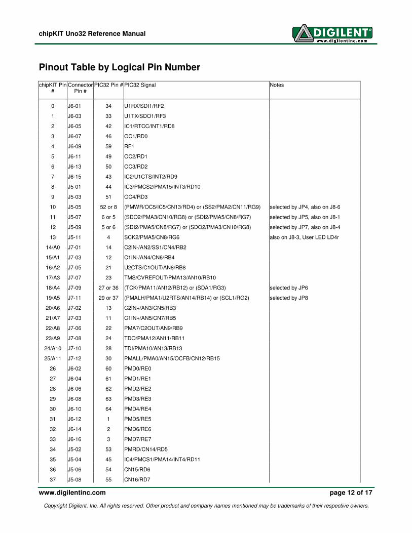
Pinout Table by Logical Pin Number chipKIT Pin
# Connector
Pin # PIC32 Pin # PIC32 Signal Notes
0 J6-01 34 U1RX/SDI1/RF2
1 J6-03 33 U1TX/SDO1/RF3
2 J6-05 42 IC1/RTCC/INT1/RD8
3 J6-07 46 OC1/RD0
4 J6-09 59 RF1
5 J6-11 49 OC2/RD1
6 J6-13 50 OC3/RD2
7 J6-15 43 IC2/U1CTS/INT2/RD9
8 J5-01 44 IC3/PMCS2/PMA15/INT3/RD10
9 J5-03 51 OC4/RD3
10 J5-05 52 or 8 (PMWR/OC5/IC5/CN13/RD4) or (SS2/PMA2/CN11/RG9) selected by JP4, also on J8-6
11 J5-07 6 or 5 (SDO2/PMA3/CN10/RG8) or (SDI2/PMA5/CN8/RG7) selected by JP5, also on J8-1
12 J5-09 5 or 6 (SDI2/PMA5/CN8/RG7) or (SDO2/PMA3/CN10/RG8) selected by JP7, also on J8-4
13 J5-11 4 SCK2/PMA5/CN8/RG6 also on J8-3, User LED LD4r
14/A0 J7-01 14 C2IN-/AN2/SS1/CN4/RB2
15/A1 J7-03 12 C1IN-/AN4/CN6/RB4
16/A2 J7-05 21 U2CTS/C1OUT/AN8/RB8
17/A3 J7-07 23 TMS/CVREFOUT/PMA13/AN10/RB10
18/A4 J7-09 27 or 36 (TCK/PMA11/AN12/RB12) or (SDA1/RG3) selected by JP6
19/A5 J7-11 29 or 37 (PMALH/PMA1/U2RTS/AN14/RB14) or (SCL1/RG2) selected by JP8
20/A6 J7-02 13 C2IN+/AN3/CN5/RB3
21/A7 J7-03 11 C1IN+/AN5/CN7/RB5
22/A8 J7-06 22 PMA7/C2OUT/AN9/RB9
23/A9 J7-08 24 TDO/PMA12/AN11/RB11
24/A10 J7-10 28 TDI/PMA10/AN13/RB13
25/A11 J7-12 30 PMALL/PMA0/AN15/OCFB/CN12/RB15
26 J6-02 60 PMD0/RE0
27 J6-04 61 PMD1/RE1
28 J6-06 62 PMD2/RE2
29 J6-08 63 PMD3/RE3
30 J6-10 64 PMD4/RE4
31 J6-12 1 PMD5/RE5
32 J6-14 2 PMD6/RE6
33 J6-16 3 PMD7/RE7
34 J5-02 53 PMRD/CN14/RD5
35 J5-04 45 IC4/PMCS1/PMA14/INT4/RD11
36 J5-06 54 CN15/RD6
37 J5-08 55 CN16/RD7
chipKIT Uno32 Reference Manual
www.digilentinc.com page 13 of 17
Copyright Digilent, Inc. All rights reserved. Other product and company names mentioned may be trademarks of their respective owners.
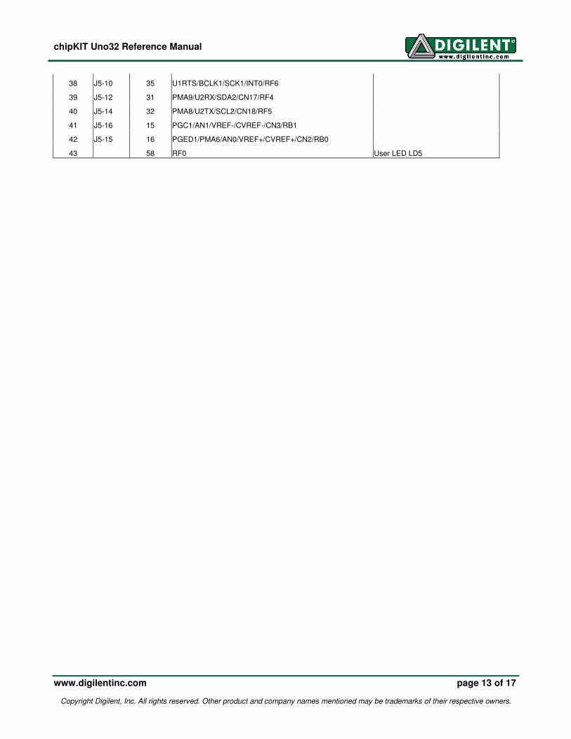
38 J5-10 35 U1RTS/BCLK1/SCK1/INT0/RF6
39 J5-12 31 PMA9/U2RX/SDA2/CN17/RF4
40 J5-14 32 PMA8/U2TX/SCL2/CN18/RF5
41 J5-16 15 PGC1/AN1/VREF-/CVREF-/CN3/RB1
42 J5-15 16 PGED1/PMA6/AN0/VREF+/CVREF+/CN2/RB0
43 58 RF0 User LED LD5
chipKIT Uno32 Reference Manual
www.digilentinc.com page 14 of 17
Copyright Digilent, Inc. All rights reserved. Other product and company names mentioned may be trademarks of their respective owners.
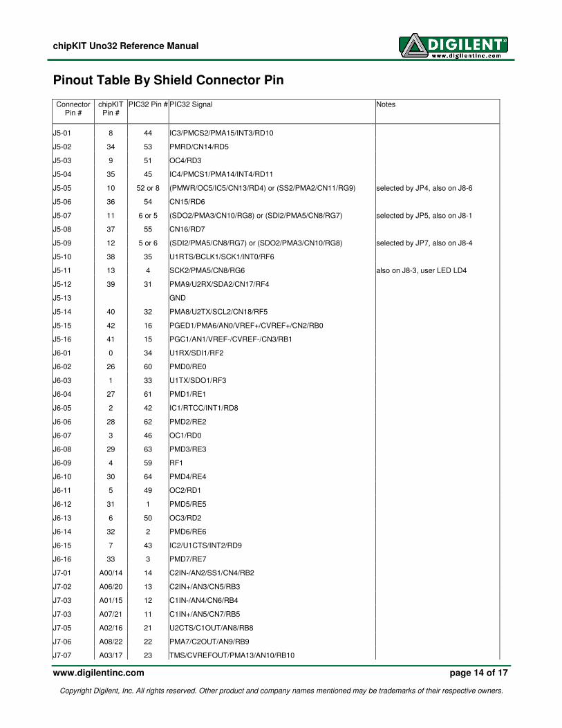
Pinout Table By Shield Connector Pin Connector
Pin # chipKIT
Pin # PIC32 Pin # PIC32 Signal Notes
J5-01 8 44 IC3/PMCS2/PMA15/INT3/RD10
J5-02 34 53 PMRD/CN14/RD5
J5-03 9 51 OC4/RD3
J5-04 35 45 IC4/PMCS1/PMA14/INT4/RD11
J5-05 10 52 or 8 (PMWR/OC5/IC5/CN13/RD4) or (SS2/PMA2/CN11/RG9) selected by JP4, also on J8-6
J5-06 36 54 CN15/RD6
J5-07 11 6 or 5 (SDO2/PMA3/CN10/RG8) or (SDI2/PMA5/CN8/RG7) selected by JP5, also on J8-1
J5-08 37 55 CN16/RD7
J5-09 12 5 or 6 (SDI2/PMA5/CN8/RG7) or (SDO2/PMA3/CN10/RG8) selected by JP7, also on J8-4
J5-10 38 35 U1RTS/BCLK1/SCK1/INT0/RF6
J5-11 13 4 SCK2/PMA5/CN8/RG6 also on J8-3, user LED LD4
J5-12 39 31 PMA9/U2RX/SDA2/CN17/RF4
J5-13 GND
J5-14 40 32 PMA8/U2TX/SCL2/CN18/RF5
J5-15 42 16 PGED1/PMA6/AN0/VREF+/CVREF+/CN2/RB0
J5-16 41 15 PGC1/AN1/VREF-/CVREF-/CN3/RB1
J6-01 0 34 U1RX/SDI1/RF2
J6-02 26 60 PMD0/RE0
J6-03 1 33 U1TX/SDO1/RF3
J6-04 27 61 PMD1/RE1
J6-05 2 42 IC1/RTCC/INT1/RD8
J6-06 28 62 PMD2/RE2
J6-07 3 46 OC1/RD0
J6-08 29 63 PMD3/RE3
J6-09 4 59 RF1
J6-10 30 64 PMD4/RE4
J6-11 5 49 OC2/RD1
J6-12 31 1 PMD5/RE5
J6-13 6 50 OC3/RD2
J6-14 32 2 PMD6/RE6
J6-15 7 43 IC2/U1CTS/INT2/RD9
J6-16 33 3 PMD7/RE7
J7-01 A00/14 14 C2IN-/AN2/SS1/CN4/RB2
J7-02 A06/20 13 C2IN+/AN3/CN5/RB3
J7-03 A01/15 12 C1IN-/AN4/CN6/RB4
J7-03 A07/21 11 C1IN+/AN5/CN7/RB5
J7-05 A02/16 21 U2CTS/C1OUT/AN8/RB8
J7-06 A08/22 22 PMA7/C2OUT/AN9/RB9
J7-07 A03/17 23 TMS/CVREFOUT/PMA13/AN10/RB10

chipKIT Uno32 Reference Manual
www.digilentinc.com page 15 of 17
Copyright Digilent, Inc. All rights reserved. Other product and company names mentioned may be trademarks of their respective owners.
J7-08 A09/23 24 TDO/PMA12/AN11/RB11
J7-09 A04/18 27 or 36 (TCK/PMA11/AN12/RB12) or (SDA1/RG3) selected by JP6
J7-10 A10/24 28 TDI/PMA10/AN13/RB13
J7-11 A05/19 29 or 37 (PMALH/PMA1/U2RTS/AN14/RB14) or (SCL1/RG2) selected by JP8
J7-12 A11/25 30 PMALL/PMA0/AN15/OCFB/CN12/RB15
chipKIT Uno32 Reference Manual
www.digilentinc.com page 16 of 17
Copyright Digilent, Inc. All rights reserved. Other product and company names mentioned may be trademarks of their respective owners.
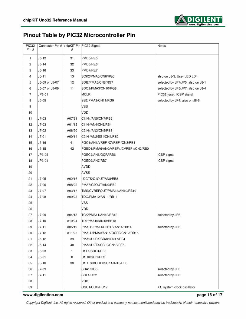
Pinout Table by PIC32 Microcontroller Pin
PIC32 Pin #
Connector Pin # chipKIT Pin #
PIC32 Signal Notes
1 J6-12 31 PMD5/RE5
2 J6-14 32 PMD6/RE6
3 J6-16 33 PMD7/RE7
4 J5-11 13 SCK2/PMA5/CN8/RG6 also on J8-3, User LED LD4
5 J5-09 or J5-07 12 SDI2/PMA5/CN8/RG7 selected by JP7/JP5, also on J8-1
6 J5-07 or J5-09 11 SDO2/PMA3/CN10/RG8 selected by JP5/JP7, also on J8-4
7 JP3-01 MCLR PIC32 reset, ICSP signal
8 J5-05 SS2/PMA2/CN11/RG9 selected by JP4, also on J8-6
9 VSS
10 VDD
11 J7-03 A07/21 C1IN+/AN5/CN7/RB5
12 J7-03 A01/15 C1IN-/AN4/CN6/RB4
13 J7-02 A06/20 C2IN+/AN3/CN5/RB3
14 J7-01 A00/14 C2IN-/AN2/SS1/CN4/RB2
15 J5-16 41 PGC1/AN1/VREF-/CVREF-/CN3/RB1
16 J5-15 42 PGED1/PMA6/AN0/VREF+/CVREF+/CN2/RB0
17 JP3-05 PGEC2/AN8/OCFARB6 ICSP signal
18 JP3-04 PGED2/AN7/RB7 ICSP signal
19 AVDD
20 AVSS
21 J7-05 A02/16 U2CTS/C1OUT/AN8/RB8
22 J7-06 A08/22 PMA7/C2OUT/AN9/RB9
23 J7-07 A03/17 TMS/CVREFOUT/PMA13/AN10/RB10
24 J7-08 A09/23 TDO/PMA12/AN11/RB11
25 VSS
26 VDD
27 J7-09 A04/18 TCK/PMA11/AN12/RB12 selected by JP6
28 J7-10 A10/24 TDI/PMA10/AN13/RB13
29 J7-11 A05/19 PMALH/PMA1/U2RTS/AN14/RB14 selected by JP8
30 J7-12 A11/25 PMALL/PMA0/AN15/OCFB/CN12/RB15
31 J5-12 39 PMA9/U2RX/SDA2/CN17/RF4
32 J5-14 40 PMA8/U2TX/SCL2/CN18/RF5
33 J6-03 1 U1TX/SDO1/RF3
34 J6-01 0 U1RX/SDI1/RF2
35 J5-10 38 U1RTS/BCLK1/SCK1/INT0/RF6
36 J7-09 SDA1/RG3 selected by JP6
37 J7-11 SCL1/RG2 selected by JP8
38 VDD
39 OSC1/CLKI/RC12 X1, system clock oscillator

chipKIT Uno32 Reference Manual
www.digilentinc.com page 17 of 17
Copyright Digilent, Inc. All rights reserved. Other product and company names mentioned may be trademarks of their respective owners.
40 OSC2/CLKO/RC15 X1, system clock oscillator
41 VSS
42 J6-05 2 IC1/RTCC/INT1/RD8
43 J6-15 7 IC2/U1CTS/INT2/RD9
44 J5-01 8 IC3/PMCS2/PMA15/INT3/RD10
45 J5-04 35 IC4/PMCS1/PMA14/INT4/RD11
46 J6-07 3 OC1/RD0
47 SOSCI/CN1/RC13 X2, secondary oscillator
48 SOSCO/T1CK/CN0/RC14 X2, secondary oscillator
49 J6-11 5 OC2/RD1
50 J6-13 6 OC3/RD2
51 J5-03 9 OC4/RD3
52 J5-05 10 PMWR/OC5/IC5/CN13/RD4 selected by JP4
53 J5-02 34 PMRD/CN14/RD5
54 J5-06 36 CN15/RD6
55 J5-08 37 CN16/RD7
56 VCAP/VDDcore
57 ENVREG
58 43 RF0 User LED LD5
59 J6-09 4 RF1
60 J6-02 26 PMD0/RE0
61 J6-04 27 PMD1/RE1
62 J6-06 28 PMD2/RE2
63 J6-08 29 PMD3/RE3
64 J6-10 30 PMD4/RE4
Top Related