


![PDTC144E series NPN resistor-equipped transistors; R1 = 47 ... · NPN resistor-equipped transistors; R1 = 47 k , R2 = 47 k 5. Limiting values Table 6. Limiting values [1] Device mounted](https://static.fdocuments.net/doc/165x107/5f6af1df5184727ecd25db5a/pdtc144e-series-npn-resistor-equipped-transistors-r1-47-npn-resistor-equipped.jpg)


Languages
Pages
Legal


DESIGN AND SIMULATION OF CMOS-BASED LOW VOLTAGE
VARIATION BANDGAP REFERENCE VOLTAGE CIRCUITRY
USING 0.18µm PROCESS TECHNOLOGY
By
TAN CHEE YONG
A Dissertation submitted for partial fulfilment of the requirement for
the degree of Master of Science (Electronic Systems Design
Engineering)
August 2015

ii
ACKNOWLEDGEMENT
First and foremost I would like to express my gratitude to my academic
supervisor, Dr. Asrulnizam Bin Abd Manaf from School of Electrical and Electronic
Engineering Universiti Sains Malaysia (USM) who has provided the perfect balance
between freedom and guidance, allowing me to obtain spherical knowledge and scope in
this field but at the same time to promptly complete my master research studies.
As part of my project research, I had the opportunity to spend time in
Collaborative Microelectronic Design Excellence Center (CEDEC) Penang. I would like
to thank Ruhaifi Abdullah Zawawi from CEDEC for his support and guidance throughout
my project. He has provided me a lot of brilliant idea and guidance in completing my
master research.
Last but not least, I would like to thank my company, Intel Microelectronics (M)
Sdn Bhd for encouraging me to further my studies in USM. Without the support from the
management team, I would not have a chance to enroll in the master program.

iii
TABLE OF CONTENTS
Page
Acknowledgement ii
Table of Contents iii
List of Tables vi
List of Figures vii
List of Abbreviations ix
List of Symbols x
Abstrak xi
Abstract xiii
CHAPTER 1 – INTRODUCTION
1.1 Background 1
1.2 Problem Statements 3
1.3 Objectives 5
1.4 Project Contributions 5
1.5 Scope of Limitation 5
1.6 Thesis Structure 6
CHAPTER 2 – LITERATURE REVIEW
2.1 Introduction 7
2.2 Operational Amplifier 7
2.2.1 Two-stage Operational Amplifier 8
2.3 Bandgap Reference Circuit 9
2.3.1 Digitally Calibrated BGR Circuit with Robust Start-up 9
Circuit and Characteristics

iv
2.3.2 Resistorless Sub-Bandgap Voltage Reference in 0.18µm CMOS 11
and Characteristics
2.3.3 Resistorless Switched-capacitor BGR with Low Sensitivity to 12
Process Variations and Characteristics
2.3.4 Low-power, Small Area and Programmable Bandgap Reference 14
And Characteristics
2.3.5 Switched-capacitor BGR Circuit with Correlated Double 17
Sampling (CDS) Techniques and Characteristics
2.3.6 Sub 1V Self-Clocked Switched Capacitor Bandgap Reference 20
Circuit and Characteristics
2.3.7 T-structure Bandgap Core Circuit and Characteristics 22
2.3.8 Simple Substhreshold BGR Circuit with Channel-length 24
Modulation Compensation and Characteristics
2.3.9 Summary of Characteristics of Different Design of BGR Circuits 25
CHAPTER 3 – METHODOLOGY
3.1 Introduction 27
3.2 Overall Design Flow of BGR Circuit 27
3.3 Operational Amplifier Circuit Design 30
3.3.1 Computation of Transistors’ Size 32
3.4 Bandgap Reference Circuit Design 37
3.4.1 VREF vs Temperature 40
3.4.2 VREF vs VDD 41
3.4.3 Power Supply Rejection Ratio (PSRR) 41
3.4.4 Temperature Coefficient (TC) 42

v
CHAPTER 4 – RESULTS AND DISCUSSION
4.1 Introduction 43
4.2 Two-stage Operational Amplifier 43
4.3 Bandgap Reference Circuit 46
4.3.1 Simulation of VREF vs Temperature 47
4.3.2 Simulation of VREF vs VDD 51
4.3.3 Simulation of Power Supply Rejection Ratio (PSRR) 52
4.3.4 Computation of Temperature Coefficient (TC) 53
CHAPTER 5 – CONCLUSION AND FUTURE WORKS
5.1 Conclusions 56
5.1 Future Works 57
REFERENCES 58
APPENDICES

vi
LIST OF TABLES
Page
Table 2.1 Summary of Characteristics of Different Design of BGR 26
Circuits
Table 3.1 Design Specifications of Two-stage Op-amp 31
Table 4.1 Transistors’ Size and Capacitors’ Value in Two-stage Op-amp 44
Table 4.2 Transistors’ Size and Resistors’ Value in BGR Circuit 47
Table 4.3 Performance Comparisons of BGR Circuits 54

vii
LIST OF FIGURES
Page
Figure 1.1 Simplified Downhole Logging Instrumentation Signal Chain 2
(Watson & Castro, 2012)
Figure 1.2 Block Diagram of Sensing System 4
Figure 2.1 Classical Two-stage Op-amp 8
(Nageshwarrao et al., 2013)
Figure 2.2 Low-voltage BGR Circuit (He.J et al., 2014) 10
Figure 2.3 Resistorless BGR Circuit (Mattia & Klimach, 2014) 11
Figure 2.4 Switch-capacitor BGR Circuit 13
(Klimach et al., 2013)
Figure 2.5 Concept of Reversed BGR (Chun & Skafidas, 2012) 15
Figure 2.6 Schematic of Programmable BGR (Chun & Skafidas, 2012) 16
Figure 2.7 Signal Processing Circuit of BGR (a) predictive phase 18
(b) calculative phase (Chen et al., 2012)
Figure 2.8 Schematic of Bandgap Circuit 20
(Wiessflecker et al., 2012)
Figure 2.9 PTAT Bias Cell (Wiessflecker et al., 2012) 21
Figure 2.10 T-structure Bandgap Reference Structure 23
(Adimulam & Movva, 2012)
Figure 2.11 Proposed Circuit with Modulation (Huang et al., 2006) 24
Figure 3.1 General Design Flow for Complete BGR Circuit 29
Figure 3.2 Schematic of Proposed Two-stage Op-amp 31
viii
Figure 3.3 Biasing Circuit for PMOS and NMOS 33
Figure 3.4 Design Flow of BGR Circuit 38
Figure 3.5 1st Order BGR Circuit 39
Figure 4.1 Two-stage Op-amp 44
Figure 4.2 Gain and Phase Margin of Two-stage Op-amp 45
Figure 4.3 Complete BGR Circuit 46
Figure 4.4 Conventional Graph of VREF vs Temperature 48
Figure 4.5 Effects of PTAT and CTAT voltage on VREF in Conventional 49
BGR Circuit
Figure 4.6(a) Graph of PTAT and CTAT Voltage in the Proposed Circuit 50
Figure 4.6(b) Graph of VREF vs Temperature of the Proposed Circuit 50
Figure 4.7 Graph of VREF vs VDD of the Proposed Circuit 51
Figure 4.8 Graph of PSRR vs Frequency in the Proposed BGR Circuit 52

ix
LIST OF ABBREVIATIONS
ADC Analog-To-Digital Converter
BGR Bandgap Reference
CMOS Complementary Metal-Oxide-Semiconductor
CTAT Complementary Proportional to Absolute Temperature
MOSFET Metal-oxide-semiconductor Field-effect Transistor
Op-amp Operational Amplifier
PLL Phase-Lock-Loop
PSRR Power Supply Rejection Ratio
PTAT Proportional to Absolute Temperature
TC Temperature Coefficient

x
LIST OF SYMBOLS
CC Compensation Capacitor
CL Load Capacitor
Cox Capacitance of the Oxide Layer
gm Transconductance of the MOSFET
VBE Base-emitter Voltage
VDD Supply Voltage
VDS Drain-source Voltage
VGS Gate-to-source Voltage
VREF Reference Voltage
Vth Threshold Voltage
VT Thermal Voltage
W/L Width over Length of the Transistor
µ Charge-carrier Effective Mobility

xi
REKABENTUK DAN SIMULASI LITAR RUJUKAN VOLTAN JURANG
JALUR YANG MEMPUNYAI VARIASI VOLTAN YANG RENDAH
BERASASKAN TEKNOLOGI PROSES CMOS 0.18µm
ABSTRAK
Pada masa kini, terdapat permintaan yang besar terhadap litar elektronik yang
mampu beroperasi secara biasa dalam persekitaran yang teruk, terutamanya dalam
persekitaran suhu yang tinggi. Untuk sistem elektronik yang digunakan dalam suhu yang
melampau, mekanisme penyejukan atau pemanasan dari sumber luaran diperlukan untuk
memastikan bahawa litar elektronik dapat berfungsi dengan baik. Pendekatan pengurusan
haba akan menyebabkan lebih banyak litar diperlukan dan pendekatan tersebut akan
meningkatkan kerumitan sistem secara keseluruhan. Oleh itu, litar pengurusan haba
luaran perlu dielakkan dan pada masa yang sama dapat memastikan bahawa sensor dapat
berfungsi pada lingkungan suhu yang besar. Oleh sebab itu, sistem pada cip yang mantap
dan dapat beroperasi dalam persekitaran yang teruk mempunyai permintaan yang besar.
Dalam projek ini, Litar Rujukan Voltan Jurang Jalur (BGR) yang terdapat dalam litar pada
cip digunakan untuk menghasilkan voltan yang tetap tanpa mengira suhu, proses and
perubahan voltan bekalan. Litar BGR yang mempunyai julat suhu yang lebar, iaitu dari -
50oC hingga 140oC, dan variasi voltan yang rendah (1.85mV) direka dan disimulasi
dengan menggunakan perisian Cadence. Litar BGR direka dengan menggunakan proses
yang serasi dengan CMOS dalam 0.18µm teknologi proses. Sebuah penguat kendalian
dua peringkat direkabentuk dan digabungkan ke dalam litar BGR yang lengkap. Simulasi
litar penguat kendalian dan litar BGR dijalankan menerusi analisis arus terus dan arus

xii
ulang-alik dalam perisian Cadence. Daripada graf-graf yang diplot, didapati bahawa litar
BGR yang dicadangkan dapat berfungsi dengan baik dalam suhu dari -50oC sampai 140oC
dengan hanya 1.85mV variasi voltan. Litar yang dicadangkan mempunyai Nisbah
Penolakan Bekalan Kuasa 38.9dB dan Pekali Suhu 7.9ppm/oC. Keputusan simulasi juga
ditanda aras dengan beberapa litar BGR yang bertahap tinggi.

xiii
DESIGN AND SIMULATION OF CMOS-BASED LOW VOLTAGE
VARIATION BANDGAP REFERENCE VOLTAGE CIRCUITRY USING 0.18µm
PROCESS TECHNOLOGY
ABSTRACT
Nowadays, electronics that are able to operate reliably in harsh environments,
especially in high temperature environments are in great demand. Electronic systems
functioning at extreme temperature requires cooling or heating mechanism from external
source. Those thermal management approaches will induce more circuitries into the
system and increase the complexity of the overall system. Thus, it is necessary to eliminate
the external thermal management circuit and at the same time, ensure that the sensors can
operate at wide range of temperature. In this project, Bandgap Reference (BGR) circuit,
which are found in on-chip circuitry, is used to produce a constant voltage regardless of
temperature, process and supply voltage change. A wide temperature range, which is -
50oC to 140oC, and low voltage variation (1.85mV) of BGR circuit was designed and
simulated using Cadence software. The BGR circuit was designed using CMOS
compatible process in 0.18µm process technology. A two-stage Operational Amplifier
(Op-amp) circuit was designed and incorporated into the complete BGR circuit. The
operational amplifier and BGR circuits were simulated using DC and AC analysis in
Cadence software. From the graphs plotted, it is found that the BGR circuit proposed is
able to operate well at temperature from -50oC to 140oC with only 1.85mV of voltage
variation. The proposed circuit has 38.9dB of PSRR and 7.9ppm/oC of Temperature
Coefficient. Simulation results are also compared with some state-of-the-art BGR circuits.
1
CHAPTER 1
INTRODUCTION
1.1 Background
Nowadays, many industries are calling for electronics that can be operated
reliably in harsh environments, especially in high temperature environments. In
automotive, defense and aerospace industries, product reliability is extremely
important. Mission-critical applications, such as safety system in an automobile,
requires electronic components that can tolerate extreme temperatures and constant
electromagnetic interference (Arvind, 2013). Traditionally, engineers had to rely on
active or passive cooling when designing electronics that must function outside normal
temperature ranges, but in some applications, cooling may not be possible or it may be
more appealing for the electronics to operate hot in order to improve system reliability
(Watson & Castro, 2012).
One of the oldest and largest user of high-temperature electronics is the
downhole oil and gas industry. The temperature in underground is high and therefore,
the electronic circuits should be robust enough to withstand the high temperature.
Active cooling is not practical in harsh environment, but passive cooling techniques
are not effective when the heating is not confined to the electronics (Watson & Castro,
2012).

2
Figure 1.1 Simplified Downhole Logging Instrumentation Signal Chain
(Watson & Castro, 2012)
Figure 1.1 shows the simplified downhole logging instrumentation process.
The sensors monitor the conditions in the underground and send the data to the
microcontroller for processing. A voltage reference circuit is needed to make sure the
electronic circuits are working well with different temperatures.
Besides the oil and gas industry, the aviation industry is also emerging for high-
temperature electronics. With the initiative to move towards the concept of “more
electric aircraft”, the aircraft industry is gearing towards to replace the traditional
centralized engine controllers with distributed control systems (Reinhardt &
Marrciniak, 1996). Converters should be placed as close as possible to the actuator
they control, thus, exposing the converters in harsh environments (Buttay et al., 2011).
Although cooling mechanism can be added into the control systems, it is still
undesirable for two reasons: cooling adds cost and weight to the aircraft, and most
importantly, failure of the cooling system could lead to failure of electronics that
control critical systems (Watson & Castro, 2012). Therefore, in advancement of
microelectronic technology, voltage reference circuit in on-chip system is critical
across these industries.

3
1.2 Problem Statement
A voltage reference circuit is an electronic circuit which produces fixed voltage
which is independent of temperature, process and supply voltage. Nowadays, Bandgap
Voltage Reference (BGR) circuit becomes a critical building block in most of the
analog and mixed signal applications, such as analog-to-digital converters (ADC), low
drop-out voltage regulators (LDO), phase-locked loops (PLL), power management
chips etc (He.J et al., 2014).
In certain circumstances, it is required that the reference voltage varies with
temperature. When the reference voltage increases with the temperature, it is known
as proportional to absolute temperature (PTAT) voltage. On the other hand, when
reference voltage decreases with the temperature, it is known as complementary to
absolute temperature (CTAT) voltage. BGR can be designed using the combinational
of PTAT voltage and CTAT voltage so that the reference circuit is independent of
temperature.
In most of the electronic systems in extreme temperature, cooling mechanism
from external source is needed to ensure the electronic circuits are able to function
properly. However, thermal management approaches introduce additional overhead
that can negatively offset the desired benefits of the electronics relative to overall
system operation (Neudeck et al., 2002). Therefore, it is necessary to eliminate the
external coolant or heater and at the same time, to ensure the sensors can operate at
wide range of temperature.

4
Apart from that, there are two major elements in most of the sensing systems
nowadays, namely CMOS sensing device and readout circuitry. The sensors, which
are the key components in the sensing systems, usually operates at voltage range of 3-
5V. However, the operating voltage of the sensors can be controlled by readout
circuitry in order to operate at lower voltages. In the digital circuits, the supply voltage
is 1.8V. Therefore, if the sensing circuity is able to operate less than 1.8V, only one
power supply is needed for both sensors and interface circuitry, as shown in Figure 1.2.
Figure 1.2 Block Diagram of Sensing System
Thus, it is important to have lesser hardware in the electronic systems in order to
reduce the complexity of the system.
Sensors Interface
circuitry Output
Power Supply
Input

5
1.3 Objectives
The objectives of this project are:
- To design and simulate a BGR circuit which having a low voltage variation
over a wide range of temperature.
i) To design and simulate an op-amp that is able to achieve high gain and
good phase margin.
ii) To characterize the performance of the BGR circuit.
1.4 Project Contributions
This research was expected to provide an alternative design topology of BGR
circuit by using CMOS process technology. The proposed BGR circuit is with simple
structure and can be operated at wide temperature range of -50oC to 140oC. Besides,
the proposed BGR circuit is having low voltage variation of 1.85mV and Temperature
Coefficient of 7.9ppm/oC.
1.5 Scope of Limitation
The aim of this research is to study and design a BGR circuit which having low
voltage variations. The scope of study is confined in the following areas:
i) The circuit designed is only in CMOS compatible process technology.
ii) Supply voltage range is 1.0V – 1.8V.
iii) Readout-circuitry is based on capacitive-difference type of sensor.

6
1.6 Thesis Structure
This thesis is organized into 5 chapters and it begins with the research
introduction and followed by research background that consists of problem statement,
research objectives, and the scope of this research. The rest of the chapters are
discussed briefly as follows:
Chapter 2 (Literature Review) introduced the basic concept of BGR circuits.
In addition, different types of BGR circuits are reviewed and compared.
Chapter 3 (Methodology and Implementation) illustrated the approaches to get
the final output result beginning from the circuit design until the simulation setup.
Chapter 4 (Results and Discussion) contained the overall results, starting from
the gain and phase-margin of op-amp, optimization effort, and followed by the graphs
of different parameters of BGR circuit.
Chapter 5 (Conclusions and Future Works) summarized the findings and data
as presented in previous chapter especially on BGR circuit and the future work in
CMOS design.
7
CHAPTER 2
LITERATURE REVIEW
2.1 Introduction
Bandgap voltage reference is first introduced by Widlar in 1970. The 5-V
voltage regulator introduced consists of three leads so that it can be supplied in
standard transistor packages (Widlar, 1970). Over the years, a lot of work has been
done to improve the performance of the BGR circuit, such as using curvature
compensation technique, reduced number of Bipolar Junction Transistors (BJT),
MOSFETs as substitute of resistors, switch-capacitor and etc. There are different goals
intended to be achieved in each paper, such as improving the Temperature Coefficient,
reducing the voltage variations, increasing the temperature range of the BGR circuit.
In this chapter, different types of BGR circuits are reviewed.
2.2 Operational Amplifier
Operation Amplifier (op-amp) is one of the most widely used electronic
devices today as the applications include industrial, consumer and scientific devices
(Nageshwarrao et al., 2013). Two-stage op-amp is one of the topologies of the op-amp
and it provides higher gain compared to single stage op-amp. Therefore, two-stage op-
amp is able to provide sufficient gain for the use in this project.

8
2.2.1 Two-stage Operational Amplifier
Op-amps are widely used in electronic devices nowadays. It is also an
important component found in the BGR circuit. In many applications, the gain of the
single-stage amplifier is often not adequate (Nageshwarrao et al., 2013). Therefore, to
achieve sufficient again, the most common type of op-amp used is two-stage op-amp
with compensation capacitors. The first stage of the op-amp provides high gain while
the second stage of the op-amp provides a large output swing (Malhotra & Description,
2013).
Figure 2.1 Classical Two-stage Op-amp (Nageshwarrao et al., 2013)
Figure 2.1 shows the classical two-stage op-amp configuration. Transistor M5
provides biasing for the entire amplifier while M1 and M2 form a differential pair of
the input to the amplifier (Nageshwarrao et al., 2013). Transistor M5 and M7 supply
the differential pair with bias current and transistor M3 and M4 form a current mirror.

9
The second stage of the op-amp is formed by M6, which is a common-source amplifier
actively loaded with the transistor M7 (Nageshwarrao et al., 2013). The total gain of
the amplifier is the summation of the gain in the first stage and second stage. The
compensation capacitor CC is added to achieve the gain frequency characteristic with
dominant pole (Blakiewicz, 2010).
2.3 Bandgap Reference Circuit
Bandgap reference (BGR) circuits are widely used in applications such as
phase locked loops, power management chips and etc (Adimulam & Movva, 2012).
Due to the importance of the BGR circuit, more and more techniques have been
proposed to improve the performance of BGR circuit over the years.
2.3.1 Digitally Calibrated BGR Circuit with Robust Start-up Circuit and
Characteristics
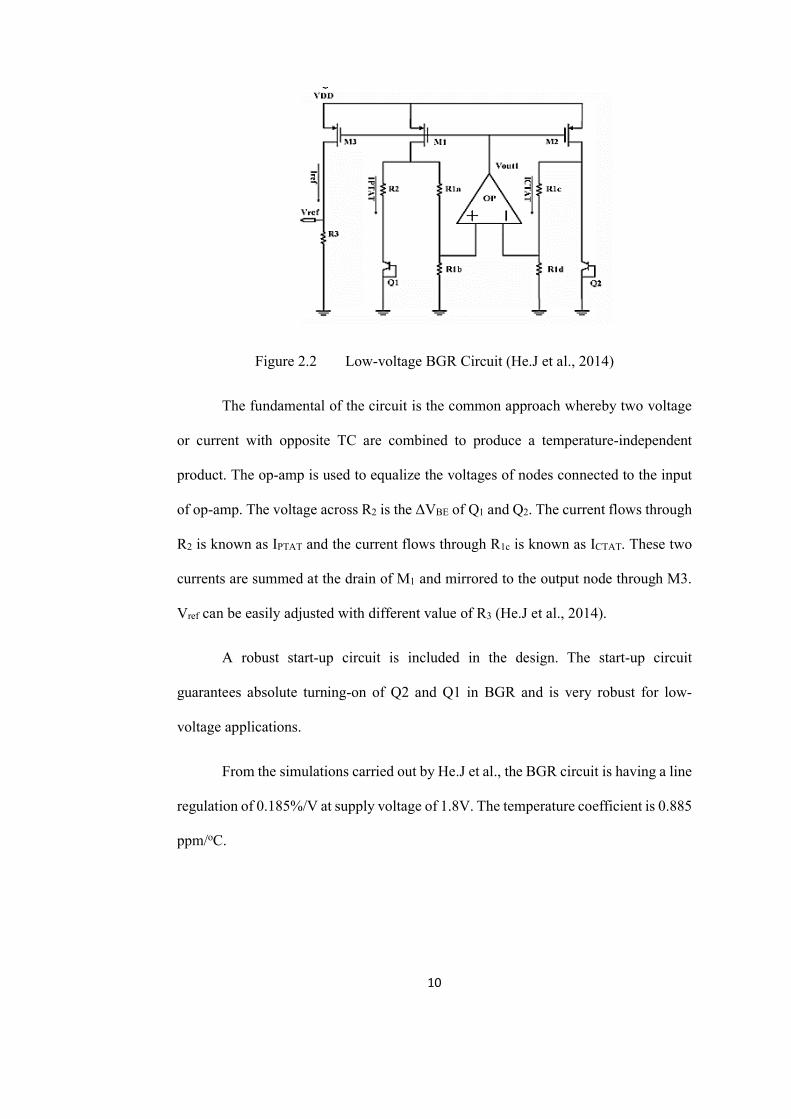
The Digitally Calibrated BGR Circuit with robust start-up circuit was proposed
by He.J et al. in 2014. According to the authors, one of the reasons that limit the
performance of BGR circuit is the nonlinear dependence of VBE on temperature. It is
desirable to have low voltage reference with a stable and low temperature coefficient
(TC) from -40oC to 125oC (He.J et al., 2014). In the proposed design, a second op-amp
is used to generate a compensation current for the calibration scheme to obtain a higher
order curvature compensation. The basic design of the BGR circuit proposed by the
authors is shown in Figure 2.2.
10
Figure 2.2 Low-voltage BGR Circuit (He.J et al., 2014)
The fundamental of the circuit is the common approach whereby two voltage
or current with opposite TC are combined to produce a temperature-independent
product. The op-amp is used to equalize the voltages of nodes connected to the input
of op-amp. The voltage across R2 is the ΔVBE of Q1 and Q2. The current flows through
R2 is known as IPTAT and the current flows through R1c is known as ICTAT. These two
currents are summed at the drain of M1 and mirrored to the output node through M3.
Vref can be easily adjusted with different value of R3 (He.J et al., 2014).
A robust start-up circuit is included in the design. The start-up circuit
guarantees absolute turning-on of Q2 and Q1 in BGR and is very robust for low-
voltage applications.
From the simulations carried out by He.J et al., the BGR circuit is having a line
regulation of 0.185%/V at supply voltage of 1.8V. The temperature coefficient is 0.885
ppm/oC.

11
2.3.2 Resistorless Sub-Bandgap Voltage Reference in 0.18µm CMOS and
Characteristics
This paper is published by Mattia and Klimach in 2014. The authors proposed
a resistorless self-biased BGR circuit, whereby the bias junction is implemented using
a counterbalance of BJT junction voltage and MOSFET gate-source voltage (Mattia
& Klimach, 2014). The schematic of the resistorless BGR circuit is shown in Figure
2.3.
Figure 2.3 Resistorless BGR Circuit (Mattia & Klimach, 2014)
From Figure 2.3, the BJT junction voltage in Q1 is counterbalance by gate-
source voltage of two stacked nMOS transistors M1 and M2. K1 represents the gain of
the current mirror used by the feedback path of the BJT. By controlling K1 and ratio
of M1 and M2, a non-zero DC operating point can be obtained, which is representing
the behavior of BJT and the MOSFETs. Since M1 and M2 are having the same aspect
ratios and same drain current, the voltage VE appears to be divided by two at the gate

12
of M1. This voltage is added to PTAT voltage generated by the cascade structures
represented by M2-M3, M4-M5 and M6-M7 to provide the temperature independent
output of VREF.
Schematic simulations was carried out by the authors using grounded-well
nMOSFETs. The effective temperature coefficient obtained is 8.79 ppm/oC for
temperature 0-125oC with VDD = 0.9V. The PSRR of the circuit is -48dB at 100Hz and
VDD 0.9V.
2.3.3 Resistorless Switched-capacitor BGR with Low Sensitivity to Process
Variations and Characteristics
A journal paper entitled “Resistorless Switched-capacitor Bandgap Voltage
Reference with Low Sensitivity to Process Variations” was written by Klimach H. et
al. in 2013. Based on the circuit topology presented by the authors, PTAT and CTAT
voltages rely on the capacitors, whereby the use of capacitors are to reduce the
sensitivity of fabrication process compared to resistors or MOS transistors. Besides,
capacitors also use less silicon area compared to resistors, where the latter needs
isolation space between adjacent lines. The switch-capacitor BGR circuit presented by
Klimach et al. is shown in Figure 2.4.

13
Figure 2.4 Switch-capacitor BGR Circuit (Klimach et al., 2013)
The VREF is only obtained after five clocking phases.
Phase 1: S1, S3, S4, S6, S7 closed.
Ca is charged to the junction voltage from Ia.
Phase 2: S2, S3, S5, S6, S7 closed.
Cb is charged to the junction voltage from Ib.
Phase 3: S1, S2, S3, S4, S5, S6 closed.
Charges in Ca and Cb are averaged out.
Phase 4: S4, S5, S6, S7 closed.
Charges transferred from C1 and C2.
VC2 = (C1/C2)[VEB(2I)-VEB(I)] = (C1/C2)(kT/q)
Phase 5: S4, S5, S7, S8, S9 closed.
C1 is inverted and connected in series with V2 and VEB(2I), resulting

14
VREF=VEB(2I) + (C1/C2)(kT/q)ln(2), which is stored in CL (Klimach et
al., 2013).
The simulation was performed in CMOS 0.18µm process. The VREF behavior
was simulated on industrial temperature range (-40oC to 85oC). According to the
authors, the designer can adjust the parameters to minimize the temperature coefficient
around the central temperature, or to minimize the effective temperature coefficient
over all temperature range. Therefore, there is a trade-off between the temperature
range and temperature coefficient. Simulations in CMOS 0.18µm process at 27 oC
shows that the VREF is approximately 1.2V with only half of the standard deviation of
traditional BGR circuit. The effective TC is 5.14 ppm/oC and allows their circuit to
be used in many applications without much calibration (Klimach et al., 2013).
2.3.4 Low-power, Small Area and Programmable Bandgap Reference and
Characteristics
A journal paper entitled “A Low-power, Small-area and Programmable
Bandgap Reference” was written by Chun & Skafidas in 2012. According to the
authors, traditional BGR circuit has no flexibility at the output voltage, as it is always
limited to around 1.2V. Therefore, they proposed a programmable BGR, featured in
sub-1V operation, low-power and small area. Two switched-capacitors are employed
to weight the temperature-dependent voltages with opposite polarity. Programmability
is achieved by controlling the closed-loop gain of the two amplifiers using reversed
BGR concept.
The concept of reversed BGR is shown in Figure 2.5 while the schematic of
programmable BGR circuit proposed by the authors is shown in Figure 2.6.
15
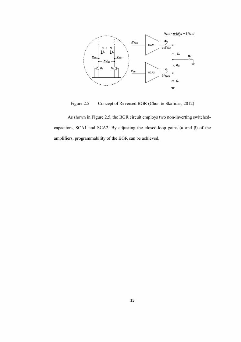
Figure 2.5 Concept of Reversed BGR (Chun & Skafidas, 2012)
As shown in Figure 2.5, the BGR circuit employs two non-inverting switched-
capacitors, SCA1 and SCA2. By adjusting the closed-loop gains (α and β) of the
amplifiers, programmability of the BGR can be achieved.

16
Figure 2.6 Schematic of Programmable BGR (Chun & Skafidas, 2012)
At Ф1, SCA1 amplifies ΔVBE with a factor of α, and saves it on capacitor C1.
SC2 generates a fraction of VBE1 with factor β. At Ф2, the summation of these two
voltages happens by stacking C1 on top of C2 (Chun & Skafidas, 2012).
The output voltage, VREF is given by
VREF = αΔVBE + βVBE1 = αVTln(N) + βVBE
where N = current density ratio of two bipolar transistors (I2/I1)

17
It is possible to generate multiple reference voltages by controlling these three
parameters (α, β and N). The BGR operates in 3 phases, Ф1(reset), Ф2(sampling),
Ф3(output).
In Ф1: C1 is charged with ΔVBE = VBE2-VBE1, C3 is charged with VBE1.
In Ф2: ΔVBE is amplified with α and saved in capacitor C5. VBE1 is scaled with
a factor of β and stored in capacitor C6.
In Ф3: VREF is obtained by summing these two voltages by stacking C5 on top
of C6.
Simulations have been carried out using 65nm CMOS process based on
different reference voltages, which are 0.591V, 0.872V and 1.189V. These reference
voltages are calculated based the design parameters from the paper “A CMOS
Bandgap Reference Circuit with Sub-1-V Operation” (Banba et al., 1999). The worst
case TC for VREF1, VREF2 and VREF3 is less than 43ppm/ oC, 28ppm/ oC, and 33ppm/ oC
respectively at the temperature range of -40 oC to 100 oC. The simulated PSRR is -
45dB at 100Hz.
2.3.5 Switched-capacitor BGR Circuit with Correlated Double Sampling (CDS)
Techniques and Characteristics
The paper “A 1-V CDS Bandgap Reference without On-Chip Resistors” was
written by Chen et al. in 2012. Based on the authors, one of the problems of
conventional BGR circuit is requirement of on-chip resistors to provide constant
current into bipolar transistors for generating PTAT/CTAT voltages. On-chip resistors
are generally having large process variation which significantly degrades the

18
performance of the Bandgap reference circuit (Chen et al., 2012). Therefore, a
switched-capacitor CMOS BGR circuit with Correlated Double Sampling (CDS) is
proposed to ease the design of high-gain amplifier in low-voltage environment.
Figure 2.7 Signal Processing Circuit of BGR: (a) predictive phase (b) calculative
phase (Chen et al., 2012)
The proposed Bandgap circuit utilizes switched-capacitor circuit to implement
the signal processing block. CDS technique is used to relax the requirement on DC
gain of the op-amp in the switched-capacitor circuit (Enz & Temes, 1996). For CDS
technique to work, there are two phases to perform the signal processing, namely
predictive phase and calculative phase, as shown in Figure 2.7.
In predictive phase, Cd_p, Cf_p and Cs_p are used to generate the output reference
voltage, Vbg_org. However, due to the offset of input op-amp, the reference voltage is
not precise enough. Therefore, there is a correction being done in the calculative phase.
19
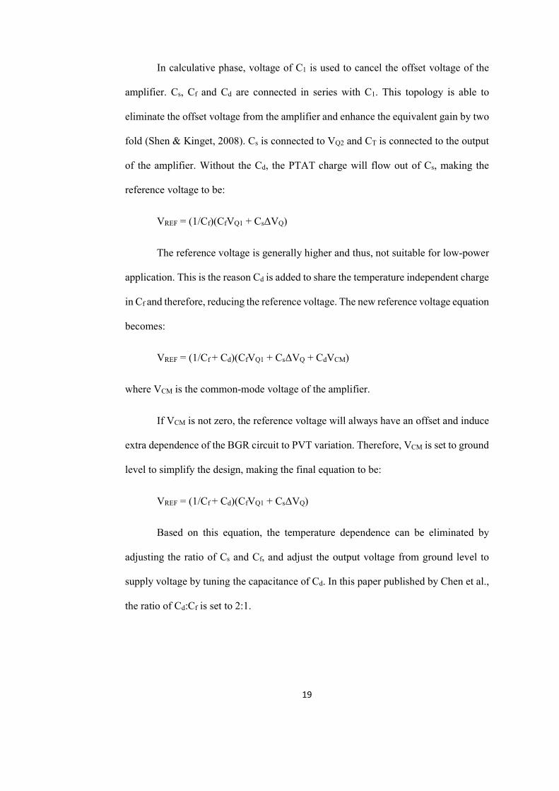
In calculative phase, voltage of C1 is used to cancel the offset voltage of the
amplifier. Cs, Cf and Cd are connected in series with C1. This topology is able to
eliminate the offset voltage from the amplifier and enhance the equivalent gain by two
fold (Shen & Kinget, 2008). Cs is connected to VQ2 and CT is connected to the output
of the amplifier. Without the Cd, the PTAT charge will flow out of Cs, making the
reference voltage to be:
VREF = (1/Cf)(CfVQ1 + CsΔVQ)
The reference voltage is generally higher and thus, not suitable for low-power
application. This is the reason Cd is added to share the temperature independent charge
in Cf and therefore, reducing the reference voltage. The new reference voltage equation
becomes:
VREF = (1/Cf + Cd)(CfVQ1 + CsΔVQ + CdVCM)
where VCM is the common-mode voltage of the amplifier.
If VCM is not zero, the reference voltage will always have an offset and induce
extra dependence of the BGR circuit to PVT variation. Therefore, VCM is set to ground
level to simplify the design, making the final equation to be:
VREF = (1/Cf + Cd)(CfVQ1 + CsΔVQ)
Based on this equation, the temperature dependence can be eliminated by
adjusting the ratio of Cs and Cf, and adjust the output voltage from ground level to
supply voltage by tuning the capacitance of Cd. In this paper published by Chen et al.,
the ratio of Cd:Cf is set to 2:1.

20
The CDS Bandgap circuit was simulated in 0.18µm CMOS process. The
supply voltage is 1.0V, which is small enough for low-power sensor applications. The
temperature dependence is 13.29 ppm/oC. The power consumption is 24.6µW.
2.3.6 Sub 1V Self-Clocked Switched Capacitor Bandgap Reference Circuit and
Characteristics
This paper entitled “A Sub 1V Self Clocked Switched Capacitor Bandgap
Reference with a Current Consumption of 180nA” was published by Wiessflecker et
al. in 2012. This paper shows the implementation of triode based Bandgap circuit with
the advantage of using only one large resistor, and still able to achieve low current
consumption. The proposed circuit consists of a Bandgap core, OTA and oscillator. As
clock is needed for the switching, a relaxation oscillator is implemented into the
reference circuit. The simplified schematic of the reference circuit is shown in Figure
2.8.
Figure 2.8 Schematic of Bandgap Circuit (Wiessflecker et al., 2012)

21
There are several transmission gates and capacitors in the circuit block. The
OTA2 works as a voltage multiplier and feed the generated reference voltage to the
output capacitor C4 (Suheng & Blalock, 2006). The core of Bandgap circuit is shown
in Figure 2.9.
Figure 2.9 PTAT Bias Cell (Wiessflecker et al., 2012)
The PTAT bias cell consists of OTA1 which consists of transistors N1 to N4
and P3 to P7 in Figure 2.9. Its purpose is to keep the voltage difference between node
A and node B as low as possible. Transistor P8 and N5 acts as an inverter, monitoring
the voltage of p-channel transistors at node D. N6 and N7 limits the maximum current
that can flow through the inverter so that there is enough current to flow through the
whole circuit. According to the authors, in standard Bandgap circuit, low values of n,
which is the area factor between two pnp-diodes, will have the disadvantage whereby
the resistor at the output node will get bigger to keep the multiplication factor of PTAT
and CTAT voltage constant. Therefore, in this topology, no resistor is needed at the
output node thus the area issue is not happening. Besides, there is no need to match the
R1 to any resistor which makes the design more robust (Wiessflecker et al., 2012).

22
CTAT voltage is at nodes A, B, C while PTAT voltage is the difference between node
A and C. The equation of voltage measured at R1 is given by:
VR1 = VA –VC = VT ln(n)
Switched capacitor is used to multiply and sum up the PTAT voltage and
CTAT voltage. Based on the paper published by Suheng & Blalock (2006), the output
voltage of OTA2 is given by:
���� =��
�� + ��∙�� +
�� + �� + ���� + ��
∙(�� − ��)
The circuit was implemented on Infineon 0.13µm CMOS process. The
reference voltage reached the intended value at around 850mV at room temperature
and stays within 2mV range over full supply variation up to 1.5V. The test chip fitted
to a temperature range from -50 to 150 oC. The temperature coefficient obtained is 41
ppm/oC.
2.3.7 T-structure Bandgap Core Circuit and Characteristics
A T-structure Bandgap core circuit was proposed by Adimulam and Movva,
2012. The circuit is able to operate at low supply voltages that can also provide low
temperature coefficient of reference voltage. According to the authors, the
conventional reference circuits is not suitable for low voltage operation because at low
voltage (Vref=1.2V), PTAT current generation is limited by collector current structure
of the vertical BJT and the input common-mode voltage of the amplifier. To eliminate
these limitations, the authors proposed a T-structure Bandgap circuitry that can operate

23
at low voltages and has low temperature coefficient due to low resistor ratios on the
design (Adimulam & Movva, 2012).
Figure 2.10 T-structure Bandgap Reference Structure (Adimulam & Movva,
2012)
Figure 2.10 shows the proposed BGV circuit by the authors. This structure
depends on two currents: one proportional to VBE which is minimum due to R2 and R3
resistors; the other current is proportional to VT by only one feedback-loop difference
(Adimulam & Movva, 2012).
Based on their simulations results, the proposed BGV circuit is having zero
temperature coefficient at 27oC and ±1.8% output voltage variation, which is sufficient
for high precision and high resolution analog circuits. The total power dissipation for
the circuit is maximum 25µW at 1.1V supply voltage. Thus, this circuit is suitable for
low power applications.

24
2.3.8 Simple Subthreshold BGR Circuit with Channel-Length Modulation
Compensation and Characteristics
A simple subthreshold CMOS Voltage Reference Circuit with Channel-Length
Modulation Compensation was proposed by Huang and Lin in 2006. The proposed
circuit consists of three parts, as shown in Figure 2.11. The first part is made of
transistors M1 to M5 and resistor R1. The second part consists of M6 to M9 with
resistor R2 while the third part consists of transistors M10 and M11 with resistor R3 to
generate the reference voltage.
Figure 2.11 Proposed Circuit with Modulation Compensation (Huang et al., 2006)
Current IA is generated by transistors M8 and M9 in subthreshold region to
obtain a PTAT current which is independent of power supply variation (Huang et al.,
2006). Current IB gives a negative temperature coefficient current, which is CTAT
Top Related