


Languages
Pages
Legal


AN12082 Capacitive Touch Sensor Design
Rev. 1.0 — 31 October 2017 Application note
Document information
Info Content
Keywords LPC845, Cap Touch
Abstract This application note describes how to design the Capacitive Touch
Sensor for the LPC845 Cap Touch Interface.
NXP Semiconductors AN12082 Capacitive Touch Sensor Design
AN12082 All information provided in this document is subject to legal disclaimers. © NXP B.V. 2017. All rights reserved.
Application note Rev. 1.0 — 31 October 2017
2 of 18
Contact information
For additional information, please visit: http://www.nxp.com
For sales office addresses, please send an email to: [email protected]
Revision history
Rev Date Description
1.0 20171031 Initial revision.

NXP Semiconductors AN12082 Capacitive Touch Sensor Design
AN12082 All information provided in this document is subject to legal disclaimers. © NXP B.V. 2017. All rights reserved.
Application note Rev. 1.0 — 31 October 2017 3 of 18
1. Introduction
In a Capacitive Touch System, the changed in capacitance when touched is converted
from charging time to count in the microcontroller.
The LPC microcontroller uses the mutual capacitance method, where a transmitting
electrode and a receiving electrode are used to generate an electromagnetic field, and
changes in the electromagnetic field between these nodes are detected.
Fig 1. Mutual Capacitive Touch
A pulse is applied between the transmitting and receiving electrode to generate an
electromagnetic field. When a finger comes into close proximity, part of the
electromagnetic field moves to the finger where the decrease in electromagnetic field
strength is detected by the electrodes. The capacitance is detected and captured, and
recognized as a finger presence.
Mutual capacitance is less noise sensitive and has less reliance on electrode
characteristics of the finger. When liquid that comes into contact with the operating
surface, it has little effect on the electromagnetic field. Thus, this method can be used
even in environments where the operating surface is likely to get wet. Mutual capacitance
is harder to use for proximity, but also has fewer false positives.
2. Touch Sensor Design
Capacitive Touch sensor design relies on the sensor and the electrodes connected to it.
The electrode's geometry, size, material, thickness, and layout affect touch sensor
measurements.

NXP Semiconductors AN12082 Capacitive Touch Sensor Design
AN12082 All information provided in this document is subject to legal disclaimers. © NXP B.V. 2017. All rights reserved.
Application note Rev. 1.0 — 31 October 2017 4 of 18
2.1 Basic Theory
Touch sensor is based on the parallel plate capacitor model in which the variation of the
capacitance C is directly proportional to the area A of two parallel plates times the
dielectric constant k of the object between them. The capacitance C is inversely
proportional to the distance d between the plates.
Fig 2. Basic PCB Capacitor
C = koA) d C is the capacitance in farads (F). A is the area of the plates in square meter d is the distance between the plates in meter (m) k is the dielectric constant of the material separating the plates
o is the permittivity of the free space (8.85 × 10¹² F/m)
2.2 Equivalent Circuit
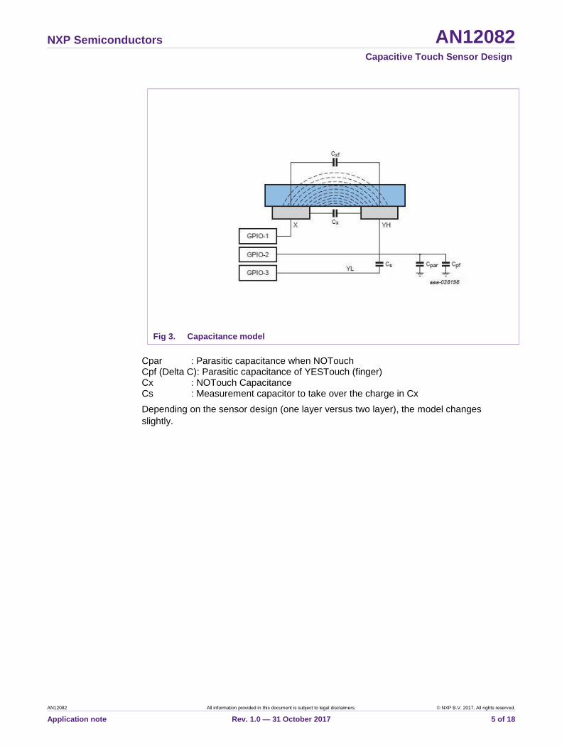
In the LPC Cap Touch interface, the mutual capacitor can be modeled as follows:
NXP Semiconductors AN12082 Capacitive Touch Sensor Design
AN12082 All information provided in this document is subject to legal disclaimers. © NXP B.V. 2017. All rights reserved.
Application note Rev. 1.0 — 31 October 2017 5 of 18
Fig 3. Capacitance model
Cpar : Parasitic capacitance when NOTouch Cpf (Delta C): Parasitic capacitance of YESTouch (finger) Cx : NOTouch Capacitance Cs : Measurement capacitor to take over the charge in Cx
Depending on the sensor design (one layer versus two layer), the model changes
slightly.
NXP Semiconductors AN12082 Capacitive Touch Sensor Design
AN12082 All information provided in this document is subject to legal disclaimers. © NXP B.V. 2017. All rights reserved.
Application note Rev. 1.0 — 31 October 2017 6 of 18
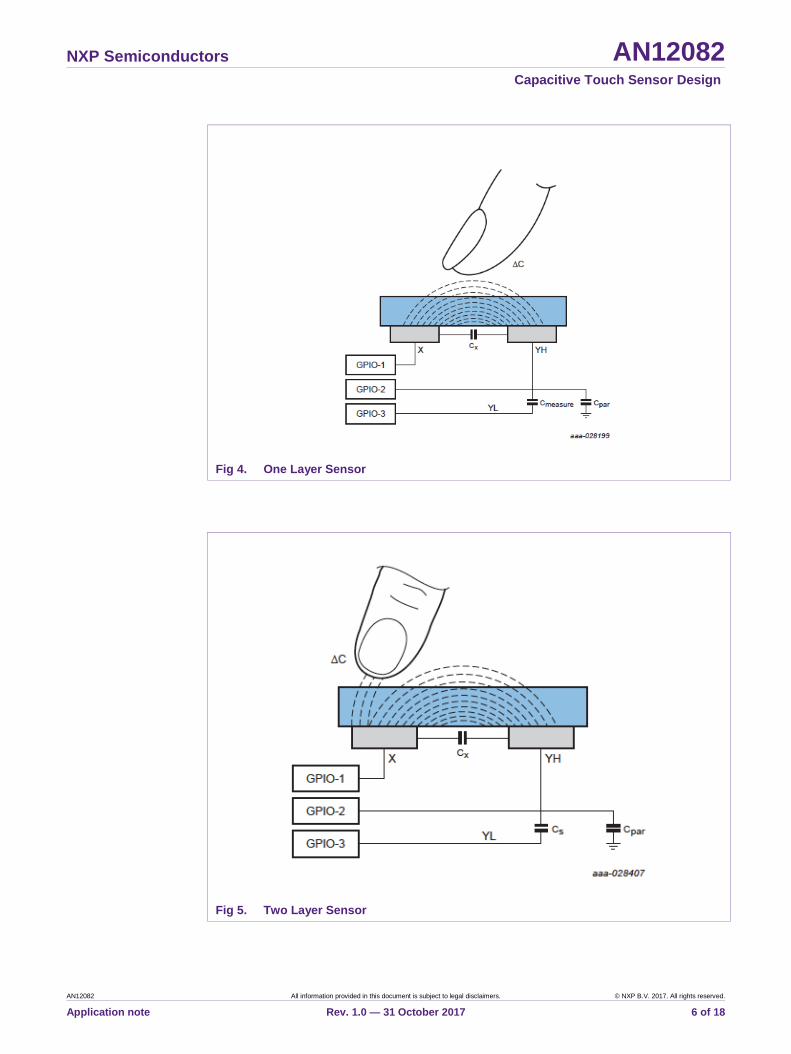
Fig 4. One Layer Sensor
Fig 5. Two Layer Sensor

NXP Semiconductors AN12082 Capacitive Touch Sensor Design
AN12082 All information provided in this document is subject to legal disclaimers. © NXP B.V. 2017. All rights reserved.
Application note Rev. 1.0 — 31 October 2017 7 of 18
The sensor characteristics will determine the SW detection details. See the Applications note on SW for Cap touch.
2.3 Sensor design
The Cap Touch peripheral support the following types of sensor design.
Fig 6. Zero and One Dimensional Sensors
Having good sensor layout determine how well the Cap touch system will work. It is
important to keep the sensor design consistent to get good Touch/No Touch results.
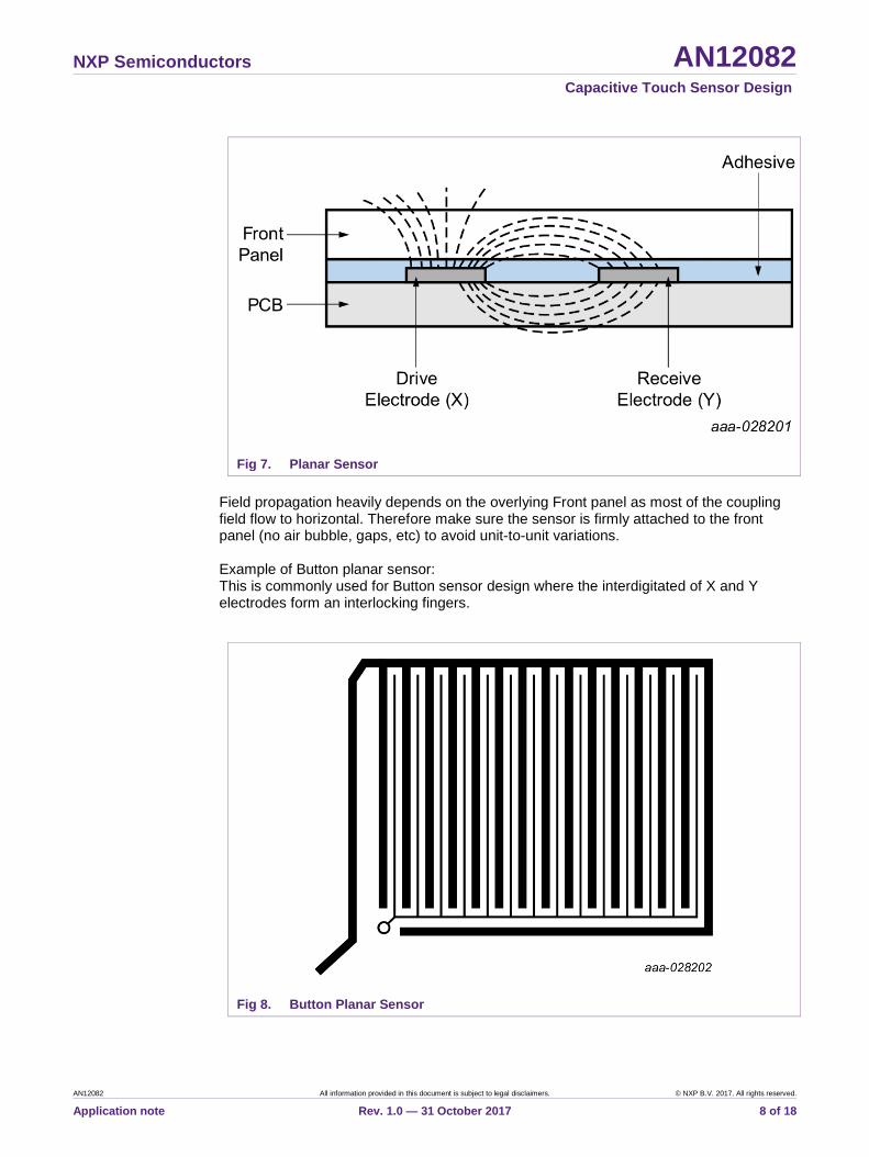
2.3.1 Planar Design
In planar construction, both sensor electrodes and traces are on the same plane. The
capacitor is formed with the electrodes and with air and the sensor Front panel material
acting as dielectric. Note both Zero and One dimensional sensors can be constructed in
Planar Design.
NXP Semiconductors AN12082 Capacitive Touch Sensor Design
AN12082 All information provided in this document is subject to legal disclaimers. © NXP B.V. 2017. All rights reserved.
Application note Rev. 1.0 — 31 October 2017 8 of 18
Fig 7. Planar Sensor
Field propagation heavily depends on the overlying Front panel as most of the coupling field flow to horizontal. Therefore make sure the sensor is firmly attached to the front panel (no air bubble, gaps, etc) to avoid unit-to-unit variations. Example of Button planar sensor: This is commonly used for Button sensor design where the interdigitated of X and Y electrodes form an interlocking fingers.
Fig 8. Button Planar Sensor

NXP Semiconductors AN12082 Capacitive Touch Sensor Design
AN12082 All information provided in this document is subject to legal disclaimers. © NXP B.V. 2017. All rights reserved.
Application note Rev. 1.0 — 31 October 2017 9 of 18
Placement of adjacent buttons should have a minimum spacing of 10mm sensor edge to
edge, to reduce cross coupling. For applications which require Gesture recognition using
9 buttons, placing Capacitive Touch sensors with <5mm spacing is necessary.
2.3.2 Slider and Wheel Design
Sliders are used for control requiring gradual adjustments. Examples include lighting
control (dimmer), volume control, graphic equalizer, and speed control. A slider is
constructed using an array of Cap Touch sensors called segments that are placed
adjacent to one another. Actuation of one segment results in partial actuation of
physically adjacent segments.
One layer slider
Fig 9. Slider Planar Sensor
Here’s one linear slider design (Two layers)
NXP Semiconductors AN12082 Capacitive Touch Sensor Design
AN12082 All information provided in this document is subject to legal disclaimers. © NXP B.V. 2017. All rights reserved.
Application note Rev. 1.0 — 31 October 2017 10 of 18
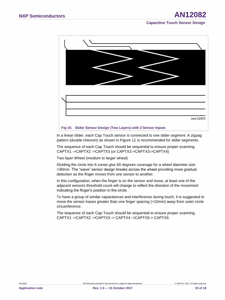
Fig 10. Slider Sensor Design (Two Layers) with 3 Sensor Inputs
In a linear slider, each Cap Touch sensor is connected to one slider segment. A zigzag
pattern (double chevron) as shown in Figure 11 is recommended for slider segments.
The sequence of each Cap Touch should be sequential to ensure proper scanning.
CAPTX1 ->CAPTX2 ->CAPTX3 (or CAPTX2->CAPTX3->CAPTX4)
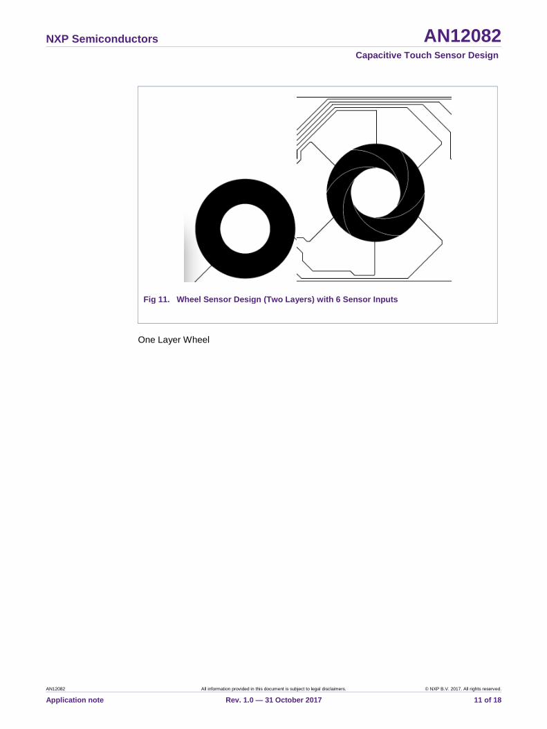
Two layer Wheel (medium to larger wheel)
Dividing the circle into 6 zones give 60 degrees coverage for a wheel diameter size
>30mm. The “wave” sensor design breaks across the wheel providing more gradual
detection as the finger moves from one sensor to another.
In this configuration, when the finger is on the sensor and move, at least one of the
adjacent sensors threshold count will change to reflect the direction of the movement
indicating the finger’s position in the circle.
To have a group of similar capacitances and interference during touch, it is suggested to
move the sensor traces greater than one finger spacing (>10mm) away from outer circle
circumference.
The sequence of each Cap Touch should be sequential to ensure proper scanning.
CAPTX1 ->CAPTX2 ->CAPTX3 -> CAPTX4 ->CAPTX5-> CAPTX6
NXP Semiconductors AN12082 Capacitive Touch Sensor Design
AN12082 All information provided in this document is subject to legal disclaimers. © NXP B.V. 2017. All rights reserved.
Application note Rev. 1.0 — 31 October 2017 11 of 18
Fig 11. Wheel Sensor Design (Two Layers) with 6 Sensor Inputs
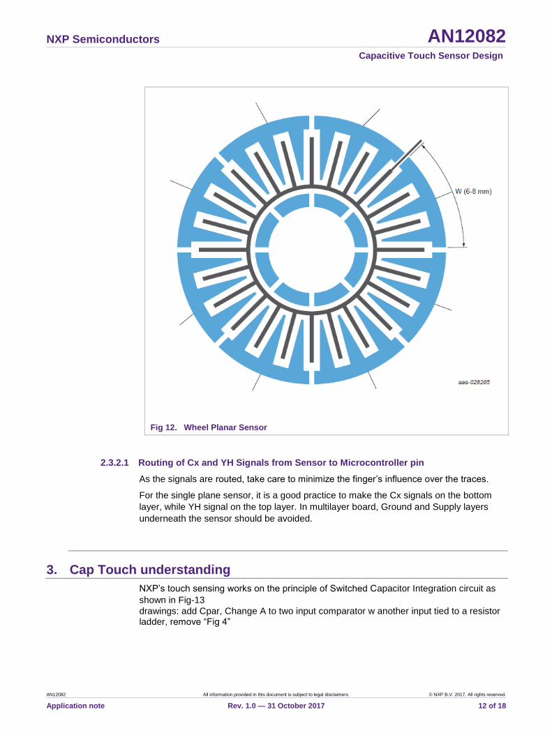
One Layer Wheel
NXP Semiconductors AN12082 Capacitive Touch Sensor Design
AN12082 All information provided in this document is subject to legal disclaimers. © NXP B.V. 2017. All rights reserved.
Application note Rev. 1.0 — 31 October 2017 12 of 18
Fig 12. Wheel Planar Sensor
2.3.2.1 Routing of Cx and YH Signals from Sensor to Microcontroller pin
As the signals are routed, take care to minimize the finger’s influence over the traces.
For the single plane sensor, it is a good practice to make the Cx signals on the bottom
layer, while YH signal on the top layer. In multilayer board, Ground and Supply layers
underneath the sensor should be avoided.
3. Cap Touch understanding
NXP’s touch sensing works on the principle of Switched Capacitor Integration circuit as
shown in Fig-13
drawings: add Cpar, Change A to two input comparator w another input tied to a resistor ladder, remove “Fig 4”

NXP Semiconductors AN12082 Capacitive Touch Sensor Design
AN12082 All information provided in this document is subject to legal disclaimers. © NXP B.V. 2017. All rights reserved.
Application note Rev. 1.0 — 31 October 2017 13 of 18
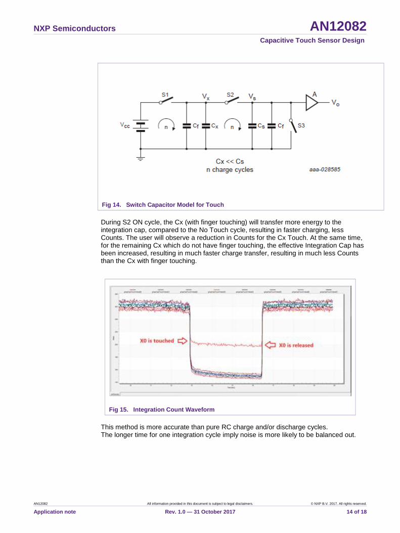
Fig 13. Switch Capacitor Model
It consists of two capacitors (Cx-Sensor and Cs -integration capacitor) controlled by switches S1 and S2, switched in non-overlapping fashion. When S1 is closed Cx charges to Vcc. Then S1 is opened and S2 is closed. This results in transfer of charge stored in Cx to Cs||Cpar until both are at same potential. This is named as one charge cycle where the charge that is first stored in Cx is shared with Cs by alternate switching of S1 and S2. The value of Cs is chosen to be very large compared to Cx, so that multiple charge cycles will be integrated onto Cs. Consequently increases the voltage of Cs. After Cs is charged to a threshold voltage, it is translated into Count, which is reported to the CPU and then discharged using S3. One complete charge cycle of Cs form one integration cycle.
3.1 Touch Occurs When a finger touches Cx, it adds Cf (delta C) from finger to Cx. As S1 is turn ON, Cx + delta C are charged to Vcc, in this case, the energy stored in Cx + Cf (delta C) > Cx (No Touch)
Note: the Cs will also increase by Cf (delta C). The additional Cf (delta C) charges up the
integration capacitance faster.
NXP Semiconductors AN12082 Capacitive Touch Sensor Design
AN12082 All information provided in this document is subject to legal disclaimers. © NXP B.V. 2017. All rights reserved.
Application note Rev. 1.0 — 31 October 2017 14 of 18
Fig 14. Switch Capacitor Model for Touch
During S2 ON cycle, the Cx (with finger touching) will transfer more energy to the integration cap, compared to the No Touch cycle, resulting in faster charging, less Counts. The user will observe a reduction in Counts for the Cx Touch. At the same time, for the remaining Cx which do not have finger touching, the effective Integration Cap has been increased, resulting in much faster charge transfer, resulting in much less Counts than the Cx with finger touching.
Fig 15. Integration Count Waveform
This method is more accurate than pure RC charge and/or discharge cycles. The longer time for one integration cycle imply noise is more likely to be balanced out.

NXP Semiconductors AN12082 Capacitive Touch Sensor Design
AN12082 All information provided in this document is subject to legal disclaimers. © NXP B.V. 2017. All rights reserved.
Application note Rev. 1.0 — 31 October 2017 15 of 18
3.2 Cap Touch Implementation in LPC845
There are up to 9 Cap Touch Sensor input Xn in the LPC845 Cap Touch module.
Each Cap Touch Sensor input perform charging/discharging/transferring charge
accumulation between X and Y plates to an external integration cap used for
measurement.
Note: Xn refers to each electrode plate (point) and Y refers to the common measurement
point (so finger correspond to each measured X).
Fig 16. Touch versus NO Touch
The time needed to get the Integration Cap (Cs) voltage to the trigger point determines it
is likely touch or partial touch. The amount of time will be reported back as Number of
Integration Cycle Counts. When it takes too long to charge the Integration Cap (during
No-Touch cycle), the Number of Counts will exceed TOUT setting, which results in
Timeout flag.
The software upper layer code will handle interpretation of results, filtering, and gestures
(if used). In addition, the upper level software handle the Sensor design: buttons, slides,
pads, etc) and configuration. The inner loop only takes measurements in the multiple of

NXP Semiconductors AN12082 Capacitive Touch Sensor Design
AN12082 All information provided in this document is subject to legal disclaimers. © NXP B.V. 2017. All rights reserved.
Application note Rev. 1.0 — 31 October 2017 16 of 18
the charge cycle. Read the Cap Touch Example Code Bundle for each sensor type
implementation.
4. Conclusion
This application note discussed the LPC84x Cap Touch implementation and the Cap
Touch Sensor design consideration to have a good cap touch sensing operation.

Erro
r!
Unkn
ow
n
do
cu
men
t
pro
pe
rty
na
me
.
Erro
r! Unkno
wn d
ocum
ent p
roperty
nam
e.
Erro
r! Un
kn
ow
n d
ocu
me
nt p
rop
erty
na
me
.
NXP Semiconductors AN12082 LPC11U3x/2x USB secondary bootloader
AN12082 All information provided in this document is subject to legal disclaimers. © NXP B.V. 2017. All rights reserved.
Application note Rev. 1.0 — 31 October 2017 17 of 18
5. Legal information
5.1 Definitions Draft — The document is a draft version only. The content is still under
internal review and subject to formal approval, which may result in
modifications or additions. NXP Semiconductors does not give any
representations or warranties as to the accuracy or completeness of
information included herein and shall have no liability for the consequences
of use of such information.
5.2 Disclaimers Limited warranty and liability — Information in this document is believed to
be accurate and reliable. However, NXP Semiconductors does not give any
representations or warranties, expressed or implied, as to the accuracy or
completeness of such information and shall have no liability for the
consequences of use of such information. NXP Semiconductors takes no
responsibility for the content in this document if provided by an information
source outside of NXP Semiconductors.
In no event shall NXP Semiconductors be liable for any indirect, incidental,
punitive, special or consequential damages (including - without limitation -
lost profits, lost savings, business interruption, costs related to the removal
or replacement of any products or rework charges) whether or not such
damages are based on tort (including negligence), warranty, breach of
contract or any other legal theory.
Notwithstanding any damages that customer might incur for any reason
whatsoever, NXP Semiconductors’ aggregate and cumulative liability
towards customer for the products described herein shall be limited in
accordance with the Terms and conditions of commercial sale of NXP
Semiconductors.
Right to make changes — NXP Semiconductors reserves the right to make
changes to information published in this document, including without
limitation specifications and product descriptions, at any time and without
notice. This document supersedes and replaces all information supplied prior
to the publication hereof.
Suitability for use — NXP Semiconductors products are not designed,
authorized or warranted to be suitable for use in life support, life-critical or
safety-critical systems or equipment, nor in applications where failure or
malfunction of an NXP Semiconductors product can reasonably be expected
to result in personal injury, death or severe property or environmental
damage. NXP Semiconductors and its suppliers accept no liability for
inclusion and/or use of NXP Semiconductors products in such equipment or
applications and therefore such inclusion and/or use is at the customer’s
own risk.
Applications — Applications that are described herein for any of these
products are for illustrative purposes only. NXP Semiconductors makes no
representation or warranty that such applications will be suitable for the
specified use without further testing or modification.
Customers are responsible for the design and operation of their applications
and products using NXP Semiconductors products, and NXP
Semiconductors accepts no liability for any assistance with applications or
customer product design. It is customer’s sole responsibility to determine
whether the NXP Semiconductors product is suitable and fit for the
customer’s applications and products planned, as well as for the planned
application and use of customer’s third party customer(s). Customers should
provide appropriate design and operating safeguards to minimize the risks
associated with their applications and products.
NXP Semiconductors does not accept any liability related to any default,
damage, costs or problem which is based on any weakness or default in the
customer’s applications or products, or the application or use by customer’s
third party customer(s). Customer is responsible for doing all necessary
testing for the customer’s applications and products using NXP
Semiconductors products in order to avoid a default of the applications and
the products or of the application or use by customer’s third party
customer(s). NXP does not accept any liability in this respect.
Export control — This document as well as the item(s) described herein
may be subject to export control regulations. Export might require a prior
authorization from competent authorities.
Evaluation products — This product is provided on an “as is” and “with all
faults” basis for evaluation purposes only. NXP Semiconductors, its affiliates
and their suppliers expressly disclaim all warranties, whether express,
implied or statutory, including but not limited to the implied warranties of non-
infringement, merchantability and fitness for a particular purpose. The entire
risk as to the quality, or arising out of the use or performance, of this product
remains with customer.
In no event shall NXP Semiconductors, its affiliates or their suppliers be
liable to customer for any special, indirect, consequential, punitive or
incidental damages (including without limitation damages for loss of
business, business interruption, loss of use, loss of data or information, and
the like) arising out the use of or inability to use the product, whether or not
based on tort (including negligence), strict liability, breach of contract, breach
of warranty or any other theory, even if advised of the possibility of such
damages.
Notwithstanding any damages that customer might incur for any reason
whatsoever (including without limitation, all damages referenced above and
all direct or general damages), the entire liability of NXP Semiconductors, its
affiliates and their suppliers and customer’s exclusive remedy for all of the
foregoing shall be limited to actual damages incurred by customer based on
reasonable reliance up to the greater of the amount actually paid by
customer for the product or five dollars (US$5.00). The foregoing limitations,
exclusions and disclaimers shall apply to the maximum extent permitted by
applicable law, even if any remedy fails of its essential purpose.
5.3 Trademarks Notice: All referenced brands, product names, service names and
trademarks are property of their respective owners.
NXP Semiconductors AN12082 Capacitive Touch Sensor Design
Please be aware that important notices concerning this document and the product(s) described herein, have been included in the section 'Legal information'.
© NXP B.V. 2017. All rights reserved.
For more information, please visit: http://www.nxp.com
For sales office addresses, please send an email to: [email protected]
Date of release: 31 October 2017
Document identifier: AN12082
6. Contents
Document information ...................................................... 1 1. Introduction ......................................................... 3 2. Touch Sensor Design ......................................... 3 2.1 Basic Theory ...................................................... 4 2.2 Equivalent Circuit ............................................... 4 2.3 Sensor design .................................................... 7 2.3.1 Planar Design ..................................................... 7 2.3.1.1 Routing of Cx and YH Signals from Sensor to
Microcontroller pin ............................................ 11 2.3.2 Slider and Wheel Design .................................... 9 3. Cap Touch understanding ................................ 11 3.1 Touch Occurs ................................................... 13 3.2 Cap Touch Implementation in LPC845 ............ 15 4. Conclusion ......................................................... 16 5. Legal information .............................................. 17 5.1 Definitions ........................................................ 17 5.2 Disclaimers....................................................... 17 5.3 Trademarks ...................................................... 17 6. Contents ............................................................. 18
Top Related