


Languages
Pages
Legal


1 Copyright © 2012, Elsevier Inc. All rights reserved.
Chapter 4
Data-Level Parallelism in
Vector, SIMD, and GPU
Architectures
Computer Architecture A Quantitative Approach, Fifth Edition

2
Contents
1. SIMD architecture
2. Vector architectures optimizations: Multiple Lanes, Vector
Length Registers, Vector Mask Registers, Memory Banks, Stride,
Scatter-Gather,
3. Programming Vector Architectures
4. SIMD extensions for media apps
5. GPUs – Graphical Processing Units
6. Fermi architecture innovations
7. Examples of loop-level parallelism
8. Fallacies
Copyright © 2012, Elsevier Inc. All rights reserved.

3 Copyright © 2012, Elsevier Inc. All rights reserved.
Flynn’s Taxonomy
SISD - Single instruction stream, single data stream
SIMD - Single instruction stream, multiple data streams New: SIMT – Single Instruction Multiple Threads (for GPUs)
MISD - Multiple instruction streams, single data stream No commercial implementation
MIMD - Multiple instruction streams, multiple data streams Tightly-coupled MIMD
Loosely-coupled MIMD
Cla
sses o
f Com
pute
rs
4 Copyright © 2012, Elsevier Inc. All rights reserved.
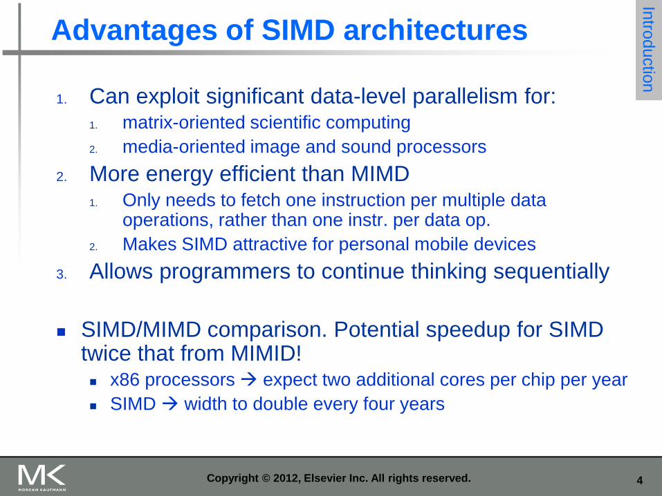
Advantages of SIMD architectures
1. Can exploit significant data-level parallelism for: 1. matrix-oriented scientific computing
2. media-oriented image and sound processors
2. More energy efficient than MIMD 1. Only needs to fetch one instruction per multiple data
operations, rather than one instr. per data op.
2. Makes SIMD attractive for personal mobile devices
3. Allows programmers to continue thinking sequentially
SIMD/MIMD comparison. Potential speedup for SIMD twice that from MIMID! x86 processors expect two additional cores per chip per year
SIMD width to double every four years
Intro
ductio
n

5 Copyright © 2012, Elsevier Inc. All rights reserved.
SIMD parallelism
SIMD architectures A. Vector architectures
B. SIMD extensions for mobile systems and multimedia applications
C. Graphics Processor Units (GPUs)
Intro
ductio
n

6 Copyright © 2012, Elsevier Inc. All rights reserved.
Figure 4.1 Potential speedup via parallelism from MIMD, SIMD, and both MIMD and SIMD over time for
x86 computers. This figure assumes that two cores per chip for MIMD will be added every two years and the
number of operations for SIMD will double every four years.
7 Copyright © 2012, Elsevier Inc. All rights reserved.
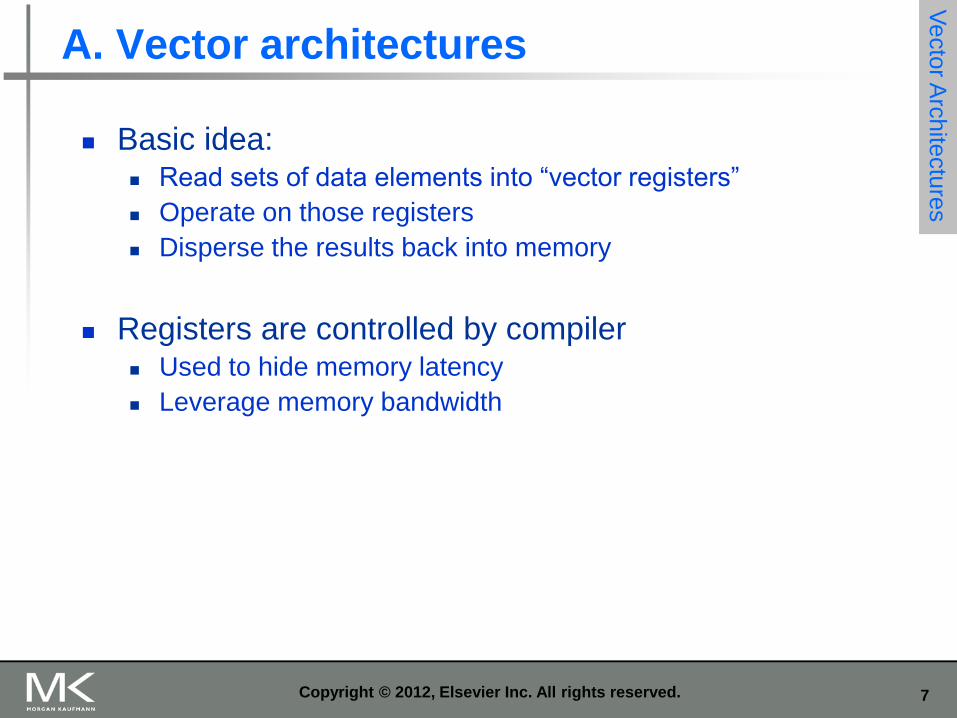
A. Vector architectures
Basic idea: Read sets of data elements into “vector registers”
Operate on those registers
Disperse the results back into memory
Registers are controlled by compiler Used to hide memory latency
Leverage memory bandwidth
Vecto
r Arc
hite
ctu
res
8 Copyright © 2012, Elsevier Inc. All rights reserved.
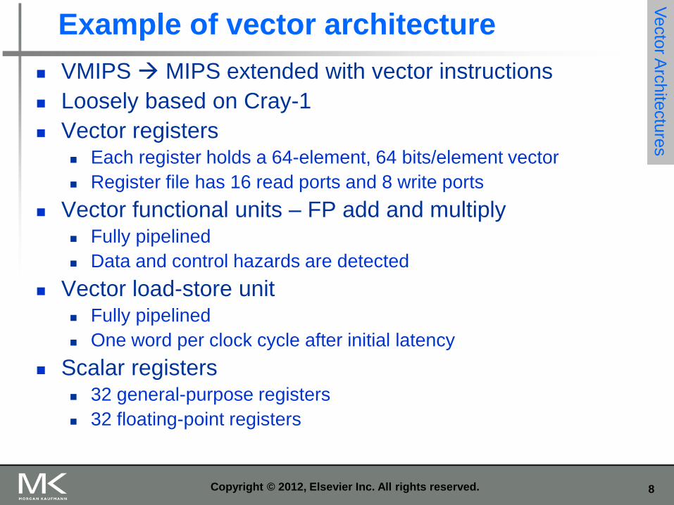
Example of vector architecture
VMIPS MIPS extended with vector instructions
Loosely based on Cray-1
Vector registers Each register holds a 64-element, 64 bits/element vector
Register file has 16 read ports and 8 write ports
Vector functional units – FP add and multiply Fully pipelined
Data and control hazards are detected
Vector load-store unit Fully pipelined
One word per clock cycle after initial latency
Scalar registers 32 general-purpose registers
32 floating-point registers
Vecto
r Arc
hite
ctu
res
9 Copyright © 2012, Elsevier Inc. All rights reserved.
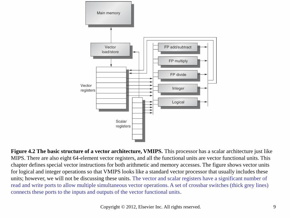
Figure 4.2 The basic structure of a vector architecture, VMIPS. This processor has a scalar architecture just like
MIPS. There are also eight 64-element vector registers, and all the functional units are vector functional units. This
chapter defines special vector instructions for both arithmetic and memory accesses. The figure shows vector units
for logical and integer operations so that VMIPS looks like a standard vector processor that usually includes these
units; however, we will not be discussing these units. The vector and scalar registers have a significant number of
read and write ports to allow multiple simultaneous vector operations. A set of crossbar switches (thick grey lines)
connects these ports to the inputs and outputs of the vector functional units.

10 Copyright © 2012, Elsevier Inc. All rights reserved.
VMIPS instructions
ADDVV.D: add two vectors.
ADDVS.D: add vector to a scalar
LV/SV: vector load and vector store from address Rx the address of vector X
Ry the address of vector Y
Example: DAXPY (double precision a*X+Y) 6 instructions
L.D F0,a ; load scalar a
LV V1,Rx ; load vector X
MULVS.D V2,V1,F0 ; vector-scalar multiply
LV V3,Ry ; load vector Y
ADDVV V4,V2,V3 ; add
SV Ry,V4 ; store the result Assumption: the vector length matches the number of vector operations – no loop necessary.
Vecto
r Arc
hite
ctu
res

11 Copyright © 2012, Elsevier Inc. All rights reserved.
DAXPY using MIPS instructions
Example: DAXPY (double precision a*X+Y)
L.D F0,a ; load scalar a
DADDIU R4,Rx,#512 ; last address to load
Loop: L.D F2,0(Rx ) ; load X[i]
MUL.D F2,F2,F0 ; a x X[i]
L.D F4,0(Ry) ; load Y[i]
ADD.D F4,F2,F2 ; a x X[i] + Y[i]
S.D F4,9(Ry) ; store into Y[i]
DADDIU Rx,Rx,#8 ; increment index to X
DADDIU Ry,Ry,#8 ; increment index to Y
SUBBU R20,R4,Rx ; compute bound
BNEZ R20,Loop ; check if done
Requires almost 600 MIPS ops when the vectors have 64
elements 64 elements of a vector x 9 ops
Vecto
r Arc
hite
ctu
res

12 Copyright © 2012, Elsevier Inc. All rights reserved.
Execution time
Vector execution time depends on: Length of operand vectors
Structural hazards
Data dependencies
VMIPS functional units consume one element per clock cycle Execution time is approximately the vector length
Convoy Set of vector instructions that could potentially execute together
Vecto
r Arc
hite
ctu
res
13 Copyright © 2012, Elsevier Inc. All rights reserved.
Chaining and chimes
Chaining Allows a vector operation to start as soon as the individual
elements of its vector source operand become available
Chime Unit of time to execute one convey
m conveys executes in m chimes
For vector length of n, requires m x n clock cycles
Sequences with read-after-write dependency hazards can be in the same convey via chaining
Vecto
r Arc
hite
ctu
res

14 Copyright © 2012, Elsevier Inc. All rights reserved.
Example
LV V1,Rx ;load vector X
MULVS.D V2,V1,F0 ;vector-scalar multiply
LV V3,Ry ;load vector Y
ADDVV.D V4,V2,V3 ;add two vectors
SV Ry,V4 ;store the sum
Three convoys:
1 LV MULVS.D first chime
2 LV ADDVV.D second chime
3 SV third chime
3 chimes, 2 FP ops per result, cycles per FLOP = 1.5
For 64 element vectors, requires 64 x 3 = 192 clock cycles
Vecto
r Arc
hite
ctu
res

15 Copyright © 2012, Elsevier Inc. All rights reserved.
Challenges
The chime model ignores the vector start-up time determined by
the pipelining latency of vector functional units
Latency of vector functional units. Assume the same as Cray-1
Floating-point add 6 clock cycles
Floating-point multiply 7 clock cycles
Floating-point divide 20 clock cycles
Vector load 12 clock cycles
Vecto
r Arc
hite
ctu
res

16
Optimizations
1. Multiple Lanes processing more than one element per clock cycle
2. Vector Length Registers handling non-64 wide vectors
3. Vector Mask Registers handling IF statements in vector code
4. Memory Banks memory system optimizations to support vector
processors
5. Stride handling multi-dimensional arrays
6. Scatter-Gather handling sparse matrices
7. Programming Vector Architectures program structures affecting
performance
Copyright © 2012, Elsevier Inc. All rights reserved.

17
1. A four lane vector unit
VIMPS instructions only allow
element N of one vector to
take part in operations
involving element N from
other vector registers this
simplifies the construction of
a highly parallel vector unit
Line contains one
portion of the vector
register file and one
execution pipeline from
each functional unit
Analog with a highway
with multiple lanes!!
Copyright © 2012, Elsevier Inc. All rights reserved.

18 Copyright © 2012, Elsevier Inc. All rights reserved.
Single versus multiple add pipelines
C= A+B
One versus four additions per
clock cycl
Each pipe adds the
corresponding elements of
the two vectors
C(i) = A(i) + B(i)
Vecto
r Arc
hite
ctu
res

19 Copyright © 2012, Elsevier Inc. All rights reserved.
2. VLR and MVL
VLR Vector Length Register; MVL Max Vector Length
Vector length:
Not known at compile time?
Not multiple of 64?
Use strip mining for vectors over the maximum length:
low = 0;
VL = (n % MVL); /*find odd-size piece using modulo op % */
for (j = 0; j <= (n/MVL); j=j+1) { /*outer loop*/
for (i = low; i < (low+VL); i=i+1) /*runs for length VL*/
Y[i] = a * X[i] + Y[i] ; /*main operation*/
low = low + VL; /*start of next vector*/
VL = MVL; /*reset length to maximum vector length*/
}
Vecto
r Arc
hite
ctu
res

20 Copyright © 2012, Elsevier Inc. All rights reserved.
3. Vector mask registers
Handling IF statements in a loop
for (i = 0; i < 64; i=i+1)
if (X[i] != 0)
X[i] = X[i] – Y[i];
If conversion use vector mask register to “disable/select”
vector elements LV V1,Rx ;load vector X into V1
LV V2,Ry ;load vector Y into V2
L.D F0,#0 ;load FP zero into F0
SNEVS.D V1,F0 ;sets VM(i) to 1 if V1(i)!=F0
SUBVV.D V1,V1,V2 ;subtract under vector mask
SV Rx,V1 ;store the result in X
GFLOPS rate decreases!
Vecto
r Arc
hite
ctu
res

21 Copyright © 2012, Elsevier Inc. All rights reserved.
4. Memory banks
Memory system must be designed to support high
bandwidth for vector loads and stores
Spread accesses across multiple banks
Control bank addresses independently
Load or store non-sequential words
Support multiple vector processors sharing the same memory
Example:
32 processors, each generating 4 loads and 2 stores/cycle
Processor cycle time is 2.167 ns, SRAM cycle time is 15 ns
How many memory banks needed?
32 processors x 6 =192 accesses,
15ns SDRAM cycle /2.167ns processor cycle≈7 processor cycles
7 x 192 1344!
Vecto
r Arc
hite
ctu
res
22 Copyright © 2012, Elsevier Inc. All rights reserved.
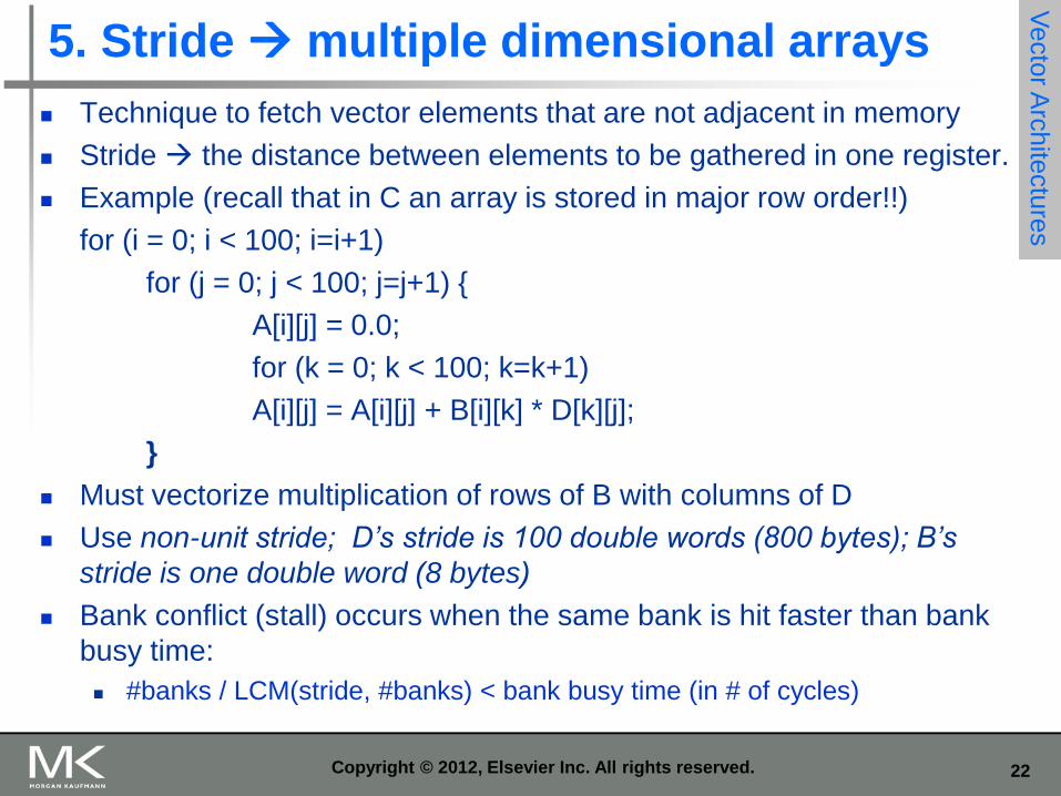
5. Stride multiple dimensional arrays
Technique to fetch vector elements that are not adjacent in memory
Stride the distance between elements to be gathered in one register.
Example (recall that in C an array is stored in major row order!!)
for (i = 0; i < 100; i=i+1)
for (j = 0; j < 100; j=j+1) {
A[i][j] = 0.0;
for (k = 0; k < 100; k=k+1)
A[i][j] = A[i][j] + B[i][k] * D[k][j];
}
Must vectorize multiplication of rows of B with columns of D
Use non-unit stride; D’s stride is 100 double words (800 bytes); B’s
stride is one double word (8 bytes)
Bank conflict (stall) occurs when the same bank is hit faster than bank
busy time:
#banks / LCM(stride, #banks) < bank busy time (in # of cycles)
Vecto
r Arc
hite
ctu
res
23 Copyright © 2012, Elsevier Inc. All rights reserved.
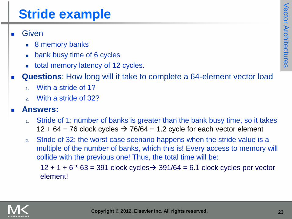
Stride example
Given
8 memory banks
bank busy time of 6 cycles
total memory latency of 12 cycles.
Questions: How long will it take to complete a 64-element vector load
1. With a stride of 1?
2. With a stride of 32?
Answers:
1. Stride of 1: number of banks is greater than the bank busy time, so it takes
12 + 64 = 76 clock cycles 76/64 = 1.2 cycle for each vector element
2. Stride of 32: the worst case scenario happens when the stride value is a
multiple of the number of banks, which this is! Every access to memory will
collide with the previous one! Thus, the total time will be:
12 + 1 + 6 * 63 = 391 clock cycles 391/64 = 6.1 clock cycles per vector
element!
Vecto
r Arc
hite
ctu
res
24 Copyright © 2012, Elsevier Inc. All rights reserved.
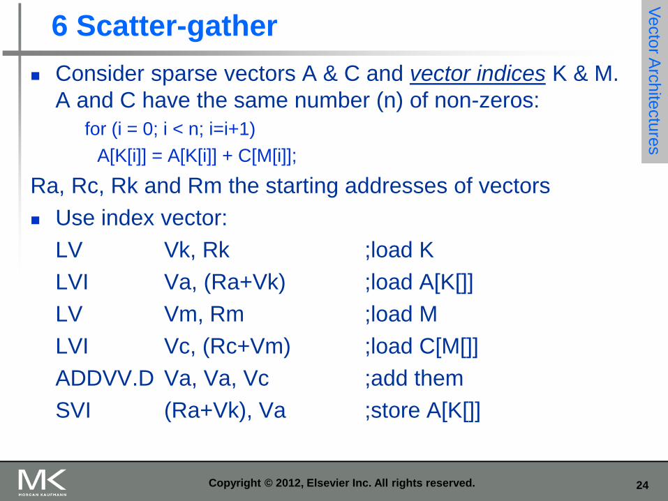
6 Scatter-gather
Consider sparse vectors A & C and vector indices K & M.
A and C have the same number (n) of non-zeros:
for (i = 0; i < n; i=i+1)
A[K[i]] = A[K[i]] + C[M[i]];
Ra, Rc, Rk and Rm the starting addresses of vectors
Use index vector:
LV Vk, Rk ;load K
LVI Va, (Ra+Vk) ;load A[K[]]
LV Vm, Rm ;load M
LVI Vc, (Rc+Vm) ;load C[M[]]
ADDVV.D Va, Va, Vc ;add them
SVI (Ra+Vk), Va ;store A[K[]]
Vecto
r Arc
hite
ctu
res

25 Copyright © 2012, Elsevier Inc. All rights reserved.
7 Programming vector architectures
Compilers can provide feedback to programmers
Programmers can provide hints to compiler
Vecto
r Arc
hite
ctu
res

26 Copyright © 2012, Elsevier Inc. All rights reserved.
Summary of vector architecture
Optimizations:
Multiple Lanes: > 1 element per clock cycle
Vector Length Registers: Non-64 wide vectors
Vector Mask Registers: IF statements in vector code
Memory Banks: Memory system optimizations to
support vector processors
Stride: Multiple dimensional matrices
Scatter-Gather: Sparse matrices
Programming Vector Architectures: Program
structures affecting performance
Vecto
r Arc
hite
ctu
res

27 Copyright © 2012, Elsevier Inc. All rights reserved.
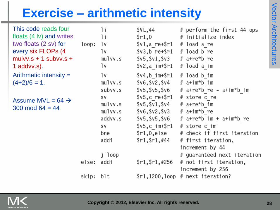
Exercise
Consider the following code, which multiplies two vectors of length 300 that
contain single-precision complex values:
For (i=0; i<300; i++) {
c_re[i] = a_re[i] * b_re[i] – a_im[i] * b_im[i];
c_im[i] = a_re[i] * b_im[i] + a_im[i] * b_re[i];
The processor runs at 700 MHz and has a maximum vector length of 64.
A. What is the arithmetic intensity of this kernel (i.e., the ratio of
floating-point operations per byte of memory accessed)?
B. Convert this loop into VMIPS assembly code using strip mining.
C. Assuming chaining and a single memory pipeline, how many
chimes are required?
Vecto
r Arc
hite
ctu
res
28
Exercise – arithmetic intensity
Copyright © 2012, Elsevier Inc. All rights reserved.
This code reads four
floats (4 lv) and writes
two floats (2 sv) for
every six FLOPs (4
mulvv.s + 1 subvv.s +
1 addvv.s).
Arithmetic intensity =
(4+2)/6 = 1.
Assume MVL = 64
300 mod 64 = 44
Vecto
r Arc
hite
ctu
res

29 Copyright © 2012, Elsevier Inc. All rights reserved.
Exercise - convoys
1. mulvv.s lv # a_re * b_re
# (assume already loaded),
# load a_im
2. lv mulvv.s # load b_im, a_im * b_im
3. subvv.s sv # subtract and store c_re
4. mulvv.s lv # a_re * b_re,
# load next a_re vector
5. mulvv.s lv # a_im * b_re,
# load next b_re vector
6. addvv.s sv # add and store c_im
6 chimes
Vecto
r Arc
hite
ctu
res

30 Copyright © 2012, Elsevier Inc. All rights reserved.
B. SIMD extensions for media apps
Media applications operate on data types narrower than the
native word size.
Graphics: 3x8-bit colors, 8-bit for transparency
Audio: 8/16/24 bit/sample
Disconnect carry chains to “partition” adder.
Example: a 256 adder can be partitioned to perform simultaneously:
32 x 8-bit additions
16 x 16-bit additions
8 x 32-bit additions
4 x 64-bit additions
Limitations, compared to vector instructions:
Number of data operands encoded into op code
No sophisticated addressing modes (strided, scatter-gather)
No mask registers
SIM
D In
stru
ctio
n S
et E
xte
nsio
ns fo
r Multim
edia

31 Copyright © 2012, Elsevier Inc. All rights reserved.
SIMD extension to x86-64 implementations Intel MMX (1996)
Eight 8-bit integer ops or four 16-bit integer ops
Streaming SIMD Extensions: (SSE) (1999), SSE3 (2004),SSE4 (2007)
Eight 16-bit integer ops
Four 32-bit integer/fp ops or two 64-bit integer/fp ops
Advanced Vector Extensions (AVE) (2010)
Four 64-bit integer/fp ops
Operands must be consecutive and at aligned memory locations
Generally designed to accelerate carefully written libraries rather
than for compilers.
Advantages over vector architecture: Cost little to add to the standard ALU
Easy to implement
Require little extra state easy for context-switching
Require little extra memory bandwidth
No virtual memory problem of cross-page access and page-fault
SIM
D In
stru
ctio
n S
et E
xte
nsio
ns fo
r Multim
edia

32 Copyright © 2012, Elsevier Inc. All rights reserved.

33 Copyright © 2012, Elsevier Inc. All rights reserved.
Example: SIMD code for DXPY; Y = Y + a X
256 – bit SIMD multimedia instructions added to MIPS.
.4D instructions operating on 4 double precision operands at once.
L.D F0,a ;load scalar a
MOV F1, F0 ;copy a into F1 for SIMD MUL
MOV F2, F0 ;copy a into F2 for SIMD MUL
MOV F3, F0 ;copy a into F3 for SIMD MUL
DADDIU R4,Rx,#512 ;last address to load
Loop: L.4D F4,0[Rx] ;load X[i], X[i+1], X[i+2], X[i+3]
MUL.4D F4,F4,F0 ;a×X[i],a×X[i+1],a×X[i+2],a×X[i+3]
L.4D F8,0[Ry] ;load Y[i], Y[i+1], Y[i+2], Y[i+3]
ADD.4D F8,F8,F4 ;a×X[i]+Y[i], ..., a×X[i+3]+Y[i+3]
S.4D F8,0[Ry] ;store into Y[i], Y[i+1], Y[i+2], Y[i+3]
DADDIU Rx,Rx,#32 ;increment index to X
DADDIU Ry,Ry,#32 ;increment index to Y
DSUBU R20,R4,Rx ;compute bound
BNEZ R20,Loop ;check if done
SIM
D In
stru
ctio
n S
et E
xte
nsio
ns fo
r Multim
edia

34 Copyright © 2012, Elsevier Inc. All rights reserved.
Roofline performance model
Basic idea:
Peak floating-point throughput as a function of arithmetic intensity
Ties together floating-point performance and memory performance
Roofline: on the sloped portion of the roof the performance is limited
by the memory bandwidth, on the flat portion it is limited by arithmetic
intensity
Arithmetic intensity Floating-point operations per byte
read
Dense matrix operations scale with problem size but sparse matrix
operations do not!!
SIM
D In
stru
ctio
n S
et E
xte
nsio
ns fo
r Multim
edia
35 Copyright © 2012, Elsevier Inc. All rights reserved.
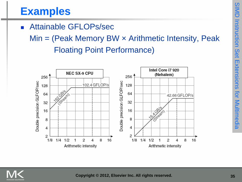
Examples
Attainable GFLOPs/sec
Min = (Peak Memory BW × Arithmetic Intensity, Peak
Floating Point Performance)
SIM
D In
stru
ctio
n S
et E
xte
nsio
ns fo
r Multim
edia

36 Copyright © 2012, Elsevier Inc. All rights reserved.
C. Graphical Processing Unit - GPU
Given the hardware invested to do graphics well, how can it
be supplemented to improve performance of a wider range
of applications?
Basic idea:
Heterogeneous execution model
CPU is the host, GPU is the device
Develop a C-like programming language for GPU
Compute Unified Device Architecture (CUDA)
OpenCL for vendor-independent language
Unify all forms of GPU parallelism as CUDA thread
Programming model: “Single Instruction Multiple Thread”
(SIMT)
Gra
phic
al P
rocessin
g U
nits
37 Copyright © 2012, Elsevier Inc. All rights reserved.
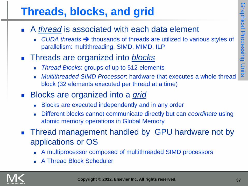
Threads, blocks, and grid
A thread is associated with each data element CUDA threads thousands of threads are utilized to various styles of
parallelism: multithreading, SIMD, MIMD, ILP
Threads are organized into blocks Thread Blocks: groups of up to 512 elements
Multithreaded SIMD Processor: hardware that executes a whole thread
block (32 elements executed per thread at a time)
Blocks are organized into a grid Blocks are executed independently and in any order
Different blocks cannot communicate directly but can coordinate using
atomic memory operations in Global Memory
Thread management handled by GPU hardware not by
applications or OS A multiprocessor composed of multithreaded SIMD processors
A Thread Block Scheduler
Gra
phic
al P
rocessin
g U
nits

38 Copyright © 2012, Elsevier Inc. All rights reserved.
NVIDIA GPU architecture
Similarities to vector machines:
Works well with data-level parallel problems
Scatter-gather transfers
Mask registers
Large register files
Differences:
No scalar processor
Uses multithreading to hide memory latency
Has many functional units, as opposed to a few deeply pipelined
units like a vector processor
Gra
phic
al P
rocessin
g U
nits
39 Copyright © 2012, Elsevier Inc. All rights reserved.
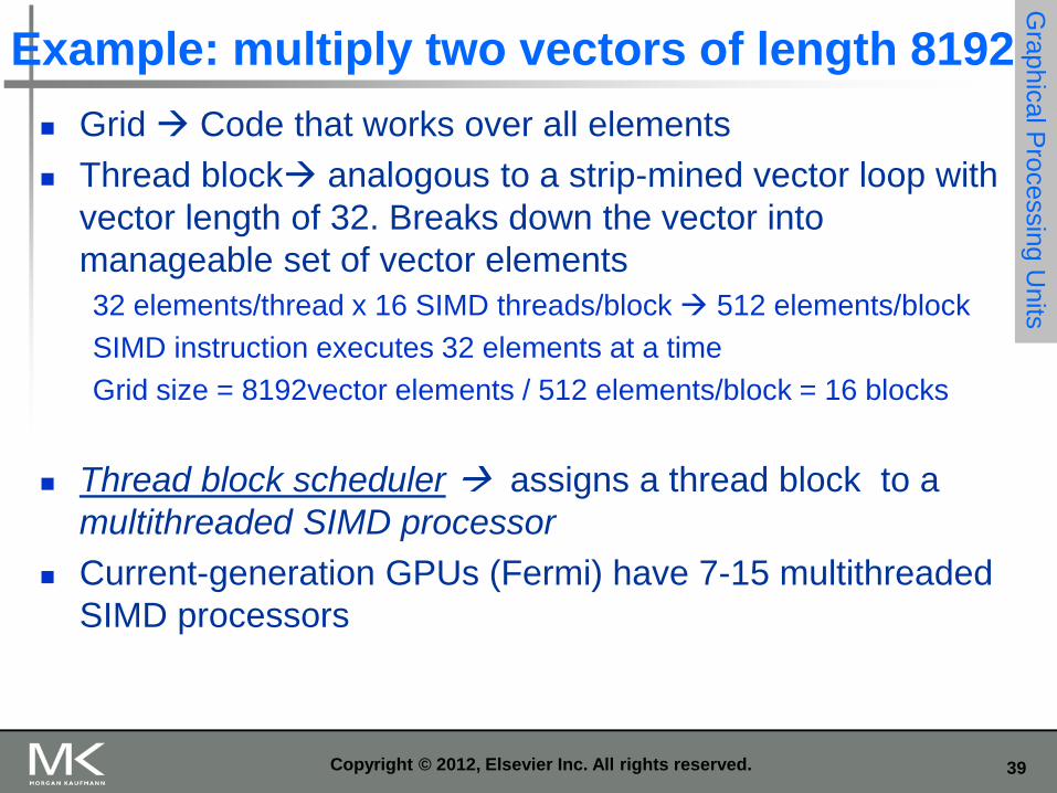
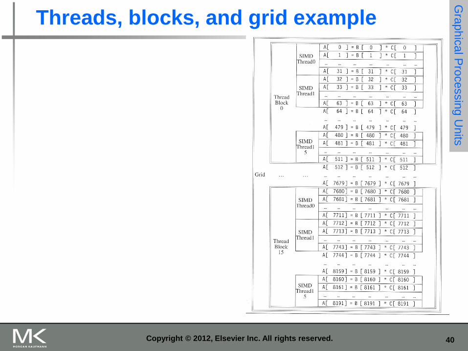
Example: multiply two vectors of length 8192
Grid Code that works over all elements
Thread block analogous to a strip-mined vector loop with
vector length of 32. Breaks down the vector into
manageable set of vector elements
32 elements/thread x 16 SIMD threads/block 512 elements/block
SIMD instruction executes 32 elements at a time
Grid size = 8192vector elements / 512 elements/block = 16 blocks
Thread block scheduler assigns a thread block to a
multithreaded SIMD processor
Current-generation GPUs (Fermi) have 7-15 multithreaded
SIMD processors
Gra
phic
al P
rocessin
g U
nits
40
Threads, blocks, and grid example
Copyright © 2012, Elsevier Inc. All rights reserved.
Gra
phic
al P
rocessin
g U
nits

41 Copyright © 2012, Elsevier Inc. All rights reserved.

42 Copyright © 2012, Elsevier Inc. All rights reserved.
Figure 4.16 Scheduling of threads of SIMD instructions. The scheduler selects a
ready thread of SIMD instructions and issues an instruction synchronously to all the
SIMD Lanes executing the SIMD thread. Because threads of SIMD instructions are
independent, the scheduler may select a different SIMD thread each time.

43
NVIDIA GPU memory structures
• Each SIMD Lane has private section of off-chip DRAM
– “Private memory”, not shared by any other lanes
– Contains stack frame, spilling registers, and private variables
– Recent GPUs cache in L1 and L2 caches
• Each multithreaded SIMD processor also has local memory that
is on-chip
– Shared by SIMD lanes / threads within a block only
• The off-chip memory shared by SIMD processors is GPU
Memory
– Host can read and write GPU memory
Gra
phic
al P
rocessin
g U
nits

44

45 Copyright © 2012, Elsevier Inc. All rights reserved.
Terminology
Threads of SIMD instructions Each has its own PC
Thread scheduler uses scoreboard to dispatch
No data dependencies between threads!
Keeps track of up to 48 threads of SIMD instructions
Hides memory latency
Thread block scheduler schedules thread blocks
to SIMD processors
Within each SIMD processor:
32 SIMD lanes
Wide and shallow compared to vector processors
Gra
phic
al P
rocessin
g U
nits

46 Copyright © 2012, Elsevier Inc. All rights reserved.
Example
NVIDIA GPU has 32,768 registers
Divided into lanes
A SIMD thread has up to:
64 vector registers of 32 32-bit elements
32 vector registers of 32 64-bit elements
Fermi has 16 physical SIMD lanes, each containing 2048
registers (2048 x 16 = 32,768)
Gra
phic
al P
rocessin
g U
nits

47 Copyright © 2012, Elsevier Inc. All rights reserved.
Figure 4.14 Simplified block diagram of a Multithreaded SIMD Processor with 16
SIMD lanes. The SIMD Thread Scheduler has, say, 48 independent threads of SIMD
instructions that it schedules with a table of 48 PCs.

48 Copyright © 2012, Elsevier Inc. All rights reserved.
NVIDIA ISA -- PTX
PTX Parallel Thread Execution
A PTX instruction describes the operation of a single CUDA thread!!
Like x86 instructions PTX instructions translate to an internal format
X86 translation done by hardware at execution time
PTX translation done by software at compile time.
The format of a PTX instruction: opcode.type d,a,b,c
d destination operand
a, b, c source operands
Use virtual registers
NVIDIA act as co-processors. Similar to I/O units
Gra
phic
al P
rocessin
g U
nits

49
PTX arithmetic instructions
Copyright © 2012, Elsevier Inc. All rights reserved.

50
PTX logical, memory access, and control flow
Copyright © 2012, Elsevier Inc. All rights reserved.

51 Copyright © 2012, Elsevier Inc. All rights reserved.
Parallel Thread Execution (PTX) example
One CUDA thread, 8192 of these created!
shl.s32 R8, blockIdx, 9 ; Thread Block ID * Block size (512 or 29)
add.s32 R8, R8, threadIdx ; R8 = i = my CUDA thread ID
ld.global.f64RD0, [X+R8] ; RD0 = X[i]
ld.global.f64RD2, [Y+R8] ; RD2 = Y[i]
mul.f64 R0D, RD0, RD4 ; Product in RD0 = RD0 * RD4 (scalar a)
add.f64 R0D, RD0, RD2 ; Sum in RD0 = RD0 + RD2 (Y[i])
st.global.f64 [Y+R8], RD0 ; Y[i] = sum (X[i]*a + Y[i])
Gra
phic
al P
rocessin
g U
nits

52 Copyright © 2012, Elsevier Inc. All rights reserved.
Conditional branching
GPU branch hardware uses:
Internal masks
Branch synchronization stack
Entries consist of masks for each SIMD lane
i.e. which threads commit their results (all threads execute)
Instruction markers to manage when a branch diverges into multiple
execution paths
Push on divergent branch
…and when paths converge
Act as barriers
Pops stack
Per-thread-lane 1-bit predicate register, specified by
programmer
Gra
phic
al P
rocessin
g U
nits

53 Copyright © 2012, Elsevier Inc. All rights reserved.
Example
if (X[i] != 0)
X[i] = X[i] – Y[i];
else X[i] = Z[i];
ld.global.f64 RD0, [X+R8] ; RD0 = X[i]
setp.neq.s32 P1, RD0, #0 ; P1 is predicate register 1
@!P1, bra ELSE1, *Push ; Push old mask, set new mask bits
; if P1 false, go to ELSE1
ld.global.f64 RD2, [Y+R8] ; RD2 = Y[i]
sub.f64 RD0, RD0, RD2 ; Difference in RD0
st.global.f64 [X+R8], RD0 ; X[i] = RD0
@P1, bra ENDIF1, *Comp ; complement mask bits
; if P1 true, go to ENDIF1
ELSE1: ld.global.f64 RD0, [Z+R8] ; RD0 = Z[i]
st.global.f64 [X+R8], RD0 ; X[i] = RD0
ENDIF1: <next instruction>, *Pop ; pop to restore old mask
Note: a thread has 64 vector components, each a 32 bit floating point
Gra
phic
al P
rocessin
g U
nits

54 Copyright © 2012, Elsevier Inc. All rights reserved.
NVIDIA GPU memory structures
Each SIMD Lane has private section of off-chip DRAM
“Private memory”, not shared by any other lanes
Contains stack frame, spilling registers, and private variables
Recent GPUs cache in L1 and L2 caches
Each multithreaded SIMD processor also has local
memory that is on-chip
Shared by SIMD lanes / threads within a block only
The off-chip memory shared by SIMD processors is GPU
Memory
Host can read and write GPU memory
Gra
phic
al P
rocessin
g U
nits
55 Copyright © 2012, Elsevier Inc. All rights reserved.
Figure 4.18 GPU Memory structures.
• GPU Memory shared by all Grids (vectorized loops),
• Local Memory shared by all threads of SIMD instructions within a thread
block (body of a vectorized loop).
• Private Memory private to a single CUDA thread.
56 Copyright © 2012, Elsevier Inc. All rights reserved.
Fermi architecture innovations
Each SIMD processor has
Two SIMD thread schedulers, two instruction dispatch units
Two sets of 16 SIMD lanes (SIMD width=32, chime=2 cycles), 16
load-store units, 4 special function units
Thus, two threads of SIMD instructions are scheduled every two
clock cycles
Fast double precision: gen- 78 515 GFLOPs for DAXPY
Caches for GPU memory: I/D L1 per SIMD processor and shared L2
64-bit addressing and unified address space: C/C++ ptrs
Error correcting codes: dependability for long-running apps
Faster context switching: hardware support, 10X faster
Faster atomic instructions: 5-20X faster than gen-
Gra
phic
al P
rocessin
g U
nits

57 Copyright © 2012, Elsevier Inc. All rights reserved.
Figure 4.19 Block Diagram of Fermi’s Dual SIMD Thread Scheduler.
Compare this design to the single SIMD Thread Design in Figure 4.16.

58 Copyright © 2012, Elsevier Inc. All rights reserved.
Fermi multithreaded SIMD processor G
raphic
al P
rocessin
g U
nits

59 Copyright © 2012, Elsevier Inc. All rights reserved.

60 Copyright © 2012, Elsevier Inc. All rights reserved.

61 Copyright © 2012, Elsevier Inc. All rights reserved.
62 Copyright © 2012, Elsevier Inc. All rights reserved.
Loop-level parallelism
Focuses on determining whether data accesses in later
iterations are dependent on data values produced in earlier
iterations
Loop-carried dependence
Example 1:
for (i=999; i>=0; i=i-1)
x[i] = x[i] + s;
No loop-carried dependence
Dete
ctin
g a
nd E
nhancin
g L
oop
-Level P
ara
llelis
m

63 Copyright © 2012, Elsevier Inc. All rights reserved.
Loop-level parallelism example 2
for (i=0; i<100; i=i+1) {
A[i+1] = A[i] + C[i]; /* S1 */
B[i+1] = B[i] + A[i+1]; /* S2 */
}
S1 and S2 use values computed by S1 in previous iteration
S2 uses value computed by S1 in same iteration
Dete
ctin
g a
nd E
nhancin
g L
oop
-Level P
ara
llelis
m

64 Copyright © 2012, Elsevier Inc. All rights reserved.
Loop-level parallelism example 3
for (i=0; i<100; i=i+1) {
A[i] = A[i] + B[i]; /* S1 */
B[i+1] = C[i] + D[i]; /* S2 */
}
S1 uses value computed by S2 in previous iteration but dependence
is not circular so loop is parallel. Transform to:
A[0] = A[0] + B[0];
for (i=0; i<99; i=i+1) {
B[i+1] = C[i] + D[i];
A[i+1] = A[i+1] + B[i+1];
}
B[100] = C[99] + D[99];
Dete
ctin
g a
nd E
nhancin
g L
oop
-Level P
ara
llelis
m
65 Copyright © 2012, Elsevier Inc. All rights reserved.
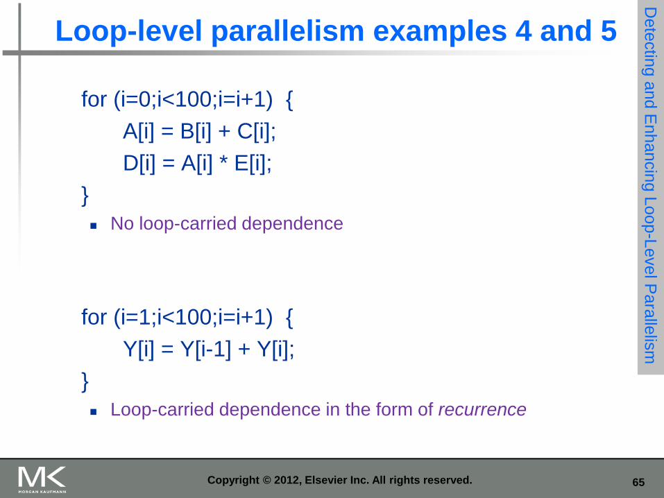
Loop-level parallelism examples 4 and 5
for (i=0;i<100;i=i+1) {
A[i] = B[i] + C[i];
D[i] = A[i] * E[i];
}
No loop-carried dependence
for (i=1;i<100;i=i+1) {
Y[i] = Y[i-1] + Y[i];
}
Loop-carried dependence in the form of recurrence
Dete
ctin
g a
nd E
nhancin
g L
oop
-Level P
ara
llelis
m

66 Copyright © 2012, Elsevier Inc. All rights reserved.
Finding dependencies
Assume that a 1-D array index i is affine:
a x i + b (with constants a and b)
An n-D array index is affine if it is affine in each dimension
Assume:
Store to a x i + b, then
Load from c x i + d
i runs from m to n
Dependence exists if:
Given j, k such that m ≤ j ≤ n, m ≤ k ≤ n
Store to a x j + b, load from a x k + d, and a x j + b = c x k + d
Dete
ctin
g a
nd E
nhancin
g L
oop
-Level P
ara
llelis
m

67 Copyright © 2012, Elsevier Inc. All rights reserved.
Finding dependencies
Generally cannot determine at compile time
Test for absence of a dependence:
GCD test:
If a dependency exists, GCD(c,a) must evenly divide (d-b)
Example:
for (i=0; i<100; i=i+1) {
X[2*i+3] = X[2*i] * 5.0;
}
Answer: a=2, b=3, c=2, d=0 GCD(c,a)=2, d-b=-3 no
dependence possible.
Dete
ctin
g a
nd E
nhancin
g L
oop
-Level P
ara
llelis
m
68 Copyright © 2012, Elsevier Inc. All rights reserved.
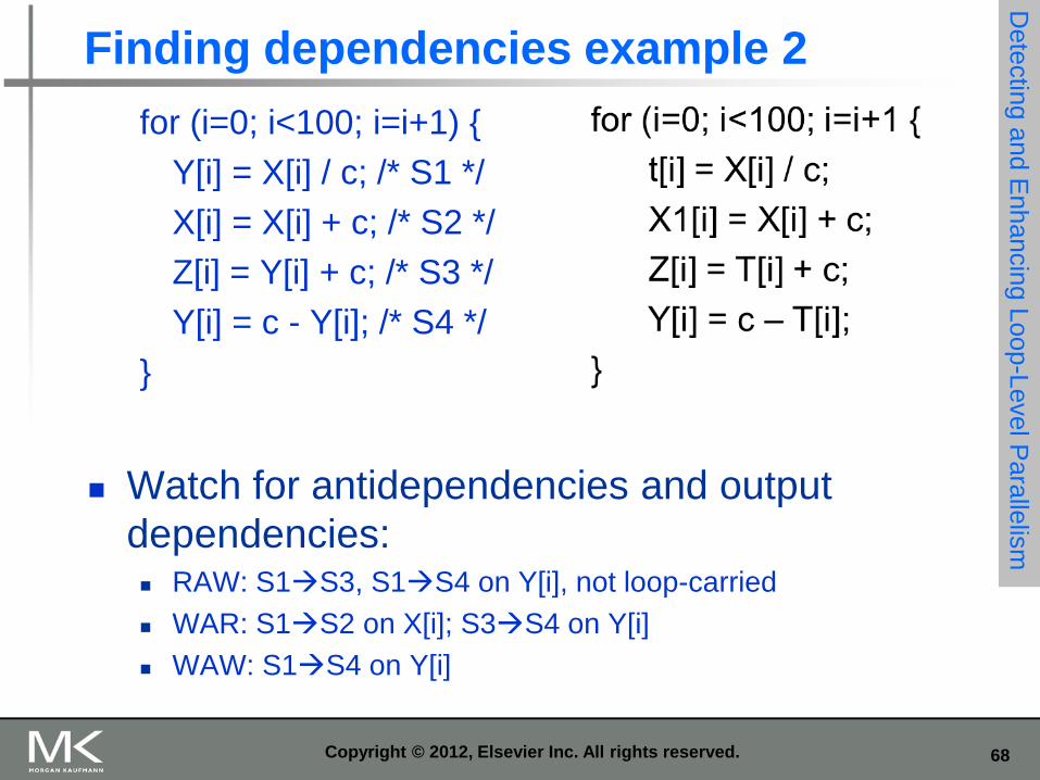
Finding dependencies example 2
for (i=0; i<100; i=i+1) {
Y[i] = X[i] / c; /* S1 */
X[i] = X[i] + c; /* S2 */
Z[i] = Y[i] + c; /* S3 */
Y[i] = c - Y[i]; /* S4 */
}
Watch for antidependencies and output
dependencies: RAW: S1S3, S1S4 on Y[i], not loop-carried
WAR: S1S2 on X[i]; S3S4 on Y[i]
WAW: S1S4 on Y[i]
Dete
ctin
g a
nd E
nhancin
g L
oop
-Level P
ara
llelis
m

69 Copyright © 2012, Elsevier Inc. All rights reserved.
Reductions
Reduction Operation:
for (i=9999; i>=0; i=i-1)
sum = sum + x[i] * y[i];
Transform to…
for (i=9999; i>=0; i=i-1)
sum [i] = x[i] * y[i];
for (i=9999; i>=0; i=i-1)
finalsum = finalsum + sum[i];
Do on p processors:
for (i=999; i>=0; i=i-1)
finalsum[p] = finalsum[p] + sum[i+1000*p];
Note: assumes associativity!
Dete
ctin
g a
nd E
nhancin
g L
oop
-Level P
ara
llelis
m
70
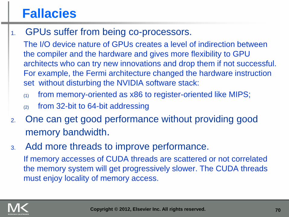
Fallacies
1. GPUs suffer from being co-processors.
The I/O device nature of GPUs creates a level of indirection between
the compiler and the hardware and gives more flexibility to GPU
architects who can try new innovations and drop them if not successful.
For example, the Fermi architecture changed the hardware instruction
set without disturbing the NVIDIA software stack:
(1) from memory-oriented as x86 to register-oriented like MIPS;
(2) from 32-bit to 64-bit addressing
2. One can get good performance without providing good
memory bandwidth.
3. Add more threads to improve performance.
If memory accesses of CUDA threads are scattered or not correlated
the memory system will get progressively slower. The CUDA threads
must enjoy locality of memory access.
Copyright © 2012, Elsevier Inc. All rights reserved.
Top Related