


Languages
Pages
Legal


A new approach to front-end electronics interfacing in the ATLAS experiment
Andrea Borga Nikhef, The Netherlands [email protected] On behalf of the ATLAS FELIX Developer Team
FELIX development team
2
John Anderson Soo Ryu Jinlong Zhang
Markus Joos Giovanna Lehmann Wainer Vandelli Benedetto Gorini Joern Schumacher
Hucheng Chen Kai Chen Waihao Wu Francesco Lanni
Frans Schreuder Andrea Borga Henk Boterenbrood Jos Vermeulen Mark Donszelmann
Julia Narevicius Alex Roich Lorne Levinson
Hucheng Chen Kai Chen Waihao Wu Francesco Lanni
Julia Narevicius Alex Roich Lorne Levinson
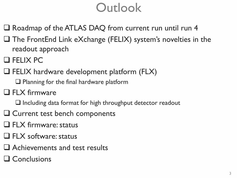
Outlook Roadmap of the ATLAS DAQ from current run until run 4 The FrontEnd Link eXchange (FELIX) system’s novelties in the
readout approach FELIX PC FELIX hardware development platform (FLX)
Planning for the final hardware platform
FLX firmware Including data format for high throughput detector readout
Current test bench components FLX firmware: status FLX software: status Achievements and test results Conclusions
3
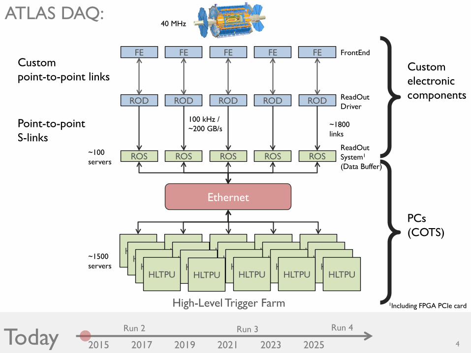
FE FE FE FE FE
Today
ATLAS DAQ:
Custom electronic components ROD ROD ROD ROD ROD
Custom point-to-point links
ReadOut Driver
HLTPU HLTPU
HLTPU HLTPU
HLTPU HLTPU
HLTPU HLTPU
HLTPU HLTPU
HLTPU HLTPU
HLTPU HLTPU
HLTPU HLTPU
HLTPU HLTPU
HLTPU HLTPU
Ethernet
PCs (COTS)
High-Level Trigger Farm
~1500 servers
40 MHz
~100 servers
ROS ROS ROS ROS ROS
Point-to-point S-links
ReadOut System1 (Data Buffer)
100 kHz / ~200 GB/s ~1800
links
1Including FPGA PCIe card
FrontEnd
4
Run 4
2015 2017 2019 2021 2023 2025
Run 3 Run 2

NSW L1 Calo Tr.
LAr Tr.
FE FE FE FE FE
ROD ROD ROD
ROS ROS ROS
HLTPU HLTPU
HLTPU HLTPU
HLTPU HLTPU
HLTPU HLTPU
HLTPU HLTPU
HLTPU HLTPU
HLTPU HLTPU
HLTPU HLTPU
HLTPU HLTPU
HLTPU HLTPU
HPC Network
Custom electronic components
High-Level Trigger Farm
Readout Readout
HPC Network
40 Gb Ethernet, Infiniband
ATLAS DAQ:
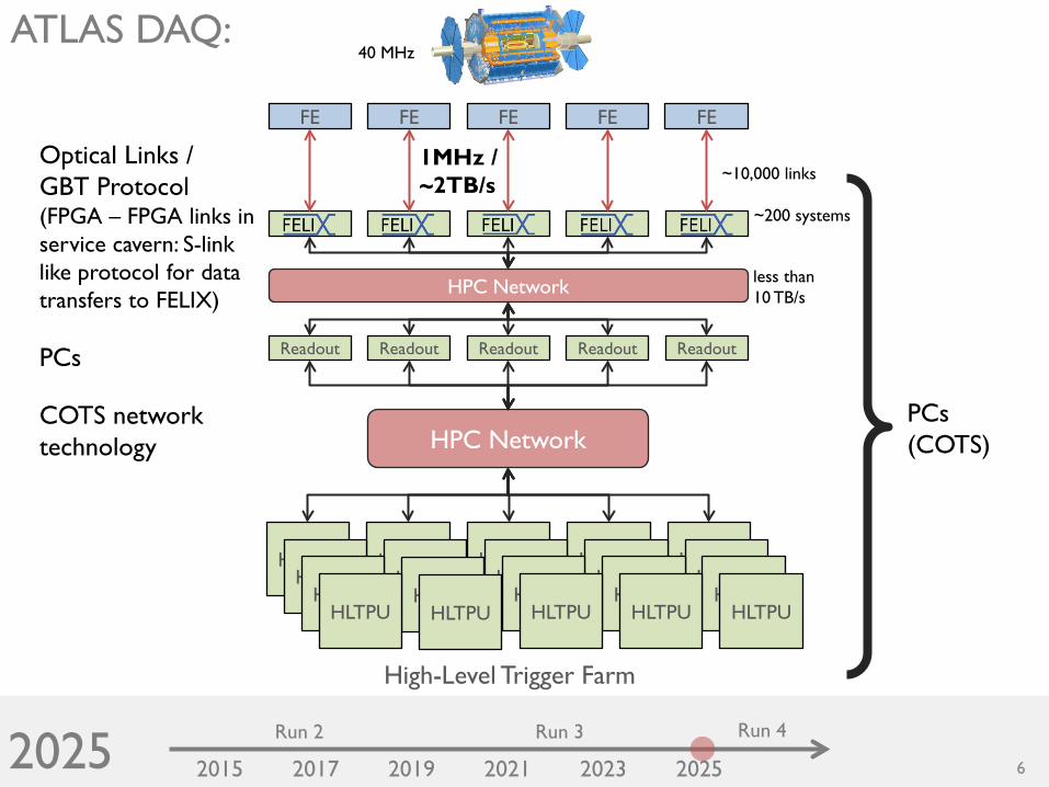
Optical links / GBT protocol (FPGA – FPGA links in service cavern: S-link like protocol for data transfers to FELIX) PCs
40 MHz New Small Wheel
PCs (COTS)
5
Run 4
2020 2015 2017 2019 2021 2023 2025
Run 3 Run 2
High Performance Computing
100 kHz / ~200 GB/s
Run 4
6
FE FE FE FE FE
Readout Readout Readout Readout Readout
HLTPU HLTPU
HLTPU HLTPU
HLTPU HLTPU
HLTPU HLTPU
HLTPU HLTPU
HLTPU HLTPU
HLTPU HLTPU
HLTPU HLTPU
HLTPU HLTPU
HLTPU HLTPU
HPC Network
Optical Links / GBT Protocol (FPGA – FPGA links in service cavern: S-link like protocol for data transfers to FELIX)
2025
High-Level Trigger Farm
HPC Network
COTS network technology
2015 2017 2019 2021 2023 2025
ATLAS DAQ: 40 MHz
~10,000 links
~200 systems
less than 10 TB/s
PCs (COTS)
Run 3 Run 2
PCs
1MHz / ~2TB/s

Scalable bidirectional architecture: off-detector end-points freed from one-to-one
geographical mapping of FE GBTs
Integrated Timing Trigger and Control (TTC), and LHC clock
distribution
Routing of multiple traffic types: physics events, detector control,
configuration, calibration, monitor
FrontEnd LInk eXchange (FELIX)
* E-link: variable-width logical link on top of the GBT protocol. Can be used to logically separate different streams on a single physical link.
SW based data processors and handlers; less custom electronics, more COTS components; flexibly upgradable (PCs, FPGAs, NICs)
7
*
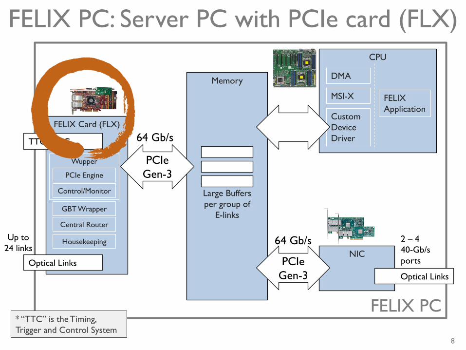
FELIX PC
FELIX Card (FLX)
Memory
Large Buffers per group of
E-links
PCIe Gen-3
Wupper
PCIe Engine
GBT Wrapper
Optical Links
CPU
Custom Device Driver
FELIX Application
MSI-X
DMA
TTC* FMC 64 Gb/s
NIC PCIe
Gen-3 Optical Links
64 Gb/s
FELIX PC: Server PC with PCIe card (FLX)
Up to 24 links
2 – 4 40-Gb/s ports
Central Router
* “TTC” is the Timing, Trigger and Control System
Housekeeping
Control/Monitor
8

FLX-710 (FELIX) HiTech Global HTG-710 Virtex-7 X690T PCIe Gen 3 x 8 lanes 2x12 bidir CXP connectors FMC connector
FLX-709 (MiniFELIX) Subset of the full FELIX functionality,
intended for FE development support Xilinx VC-709 Virtex-7 X690T PCIe Gen 3 x 8 lanes 4 SFP+ connectors FMC connector
FELIX Development Cards (FLX)
9
TTCfx Custom FMC accepting TTC input Outputs TTC clock and CH A-B info V1: ADN2814 + CDCE62005 V2: ADN2814 + Si5338

Ongoing development: BNL-711 (FLX-711)
10
BNL is developing a PCIe card for the ATLAS LAr Calorimeter Phase-I Upgrade The PCIe card will be used as the DAQ platform
for the LTDB (Liquid Argon Trigger Digitizer Board) production test stand Close collaboration with Nikhef, Weizmann and IRI Frankfurt (Heiko Engel)
on module design for the FELIX use case
Features: Xilinx Kintex Ultrascale FPGA o 64 GTH transceiver (16.375 Gb/s) 4 MiniPOD TX and 4 MiniPOD RX o 48 duplex optical links (14 Gb/s) PCIe Gen3 x16 lanes Two DDR4 SODIMM up to 16GB Onboard: o Clock conditioner (Si5338) o TTC receiver (ADN2814) o TTC BUSY lemo output
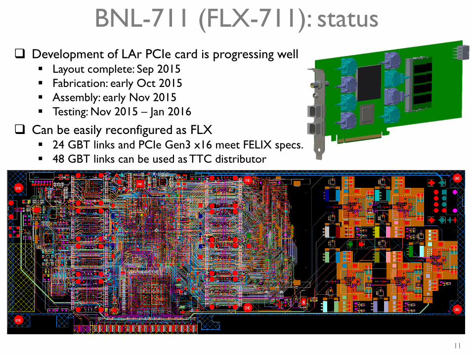
BNL-711 (FLX-711): status
11
Development of LAr PCIe card is progressing well Layout complete: Sep 2015 Fabrication: early Oct 2015 Assembly: early Nov 2015 Testing: Nov 2015 – Jan 2016
Can be easily reconfigured as FLX 24 GBT links and PCIe Gen3 x16 meet FELIX specs. 48 GBT links can be used as TTC distributor

FLX firmware simple block diagram
Software
12

GBT Wrapper FELIX “GBT-FPGA” is based on CERN GBT-FPGA, with some changes:
Ported to Xilinx Vivado Transceiver independent (Xilinx GTH, GTX, etc.) Support for quads (4 transceivers + PLLs) and a parametrized number of quads Run-time choice of GBT Normal (FEC) mode, GBT Wide mode, “Full mode”
o “Full mode” is a FELIX addition: 9.6Gb/s byte stream (encoding TBD) Lower (fixed) latency (worst cases: Tx 57.1 ns; Rx FEC 63.2ns; Rx Wide 50.7 ns)
Input/output Interfaces: 120-bit registers clocked at 40MHz
13

14
Central Router
Shown: 1 of 7 E-groups of a GBT 1 of “N” GBTs
Handles data streams: From GBT channels to
Host PC memory The opposite direction Routes TTC information Dedicated manager for
E-Links in GBT channels Main manager toward PCIe
Engine

For each E-link fixed size blocks (1 kByte) are filled with received data Each block has a 4-Byte header: E-link ID, a sequence number and a start of block symbol Data packets (“chunks”) received can be of arbitrary length and are
subdivided (typically after e.g. 8B/10B decoding) in sub-chunks as needed to fill the blocks Each sub-chunk has a trailer with information on its length and type In case of low data rates time-outs will cause incompletely filled blocks to be padded and
sent (the last sub-chunk in this block is then of type “null”) Blocks are transferred using continuous DMA (Direct Memory Access) into a large
(e.g. 4 GByte) circular buffer in host PC memory The buffer consists of contiguous memory allocated by a dedicated driver The DMA is controlled with two pointers, a write pointer maintained by the DMA
controller in the FPGA, and a read pointer maintained by the FELIX application
High throughput detector readout
15
first word transferred
last word transferred
sub-chunk
1 kB block sub- chunk
sub- chunk
1 kB block 1 kB block
* 1 kB blocks of other E-links
* *
E-link packet = chunk
1 kB block 1 kB block
fragment trailer first/last/both/middle/null (3 bits) flags: xfer error, trunc, rsrvd, rsrvd (4 bits) fragment length in 16-bit words
block header: E-link ID (11 bits) sequence number (5 bits) Start-Of-Block symbol (16-bits)

Wupper*: PCIe Engine for FELIX PCIe Engine with
DMA interface to the Xilinx Virtex-7 PCIe Gen3 Integrated Block for PCI Express (PG023)
Xilinx AXI (ARM AMBA) Stream Interface (UG761)
MSI-X compatible interrupt controller
Applications access the engine via simple FIFOs
Register map for programmed I/O synchronized to a lower clock speed
Developed for use in FELIX Published as OpenSource (LGPL) on OpenCores
http://opencores.org/project,virtex7_pcie_dma
* The person performing the act of bongelwuppen, the version from the Dutch province of Groningen of the “famous” Frisian sport Fierljeppen (canal pole vaulting) https://www.youtube.com/watch?v=YP32iWoqjnQ 16

FELIX PC: Motherboard and NIC Supermicro motherboards, e.g.: SuperMicro X9SRL-F 1x Ivy Bridge CPU, 6 cores 6x PCIe Gen-3 slots 16 GB DDR3 Memory http://www.supermicro.com/products/motherboard/Xeon/C600/X9SRL-F.cfm
SuperMicro X10DRG-Q 2x Haswell CPU, up to 10 cores 6x PCIe Gen-3 slots 64 GB DDR4 Memory http://supermicro.com/products/motherboard/Xeon/C600/X10DRG-Q.cfm
Mellanox ConnectX-3 VPI FDR/QDR Infiniband 2x10/40 GbE http://www.mellanox.com/page/products_dyn?product_family=119&mtag=connectx_3_vpi
17
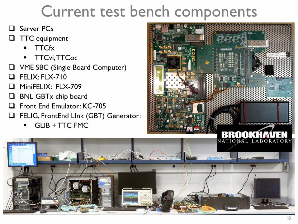
Current test bench components Server PCs TTC equipment
TTCfx TTCvi, TTCoc
VME SBC (Single Board Computer) FELIX: FLX-710 MiniFELIX: FLX-709 BNL GBTx chip board Front End Emulator: KC-705 FELIG, FrontEnd LInk (GBT) Generator:
GLIB + TTC FMC
18

FLX firmware: status FELIX (FLX-710, HTG-710)
8 channels with local loopback works Data generated by internal data generators Scaling to more channels ongoing Improving overall fitting in the FPGA Improving overall firmware reliability
MiniFELIX (FLX-709, VC-709) 4 channels with local loopback works physical connectivity OK Improving reliability
19
VC-709
HTG-710
TTCfx
TTCfx

FLX software: status Growing ecosystem of low level and debugging tools
Board communication and control
Data flow control and check
Performance testing
QT based GUI for various configuration and control
Loading emulator data in FPGA RAM works
Defined software stack
Define interfaces for interoperability
Split development effort among software designers
Documenting software
20
loopback via GBT links of data from internal generator
HW peripheral monitor
various card statuses
various card info

Achievements
Wupper: PCIe DMA transfers to Host memory demonstrated Simple counter with direct connection GBT Emulator through Central Router
CentralRouter: E-proc based data routing demonstrated for 8 GBT links GBT Wrapper: GBT links software calibration (“training”) and monitoring Tested bidirectional communication from GBT Wrapper to Front-End
GBT Emulated data TTC information (L1As, clock)
In parallel developed and tested data handling software See papers at DEBS and CHEP conferences
21
Conclusions
22
The FrontEnd LInk eXchange (FELIX) is a PC based Data Acquisition system designed for bridging custom links (GBT) to a COTS computer network
It is designed to be flexible and highly-configurable
Development is progressing well and according to schedule
A scaled (sub-set of the full functionality) demonstrator had been positively reviewed in May 2015
Support for data transfers to Front-End is to be implemented
Scaling to more channels is to be implemented
Final design review foreseen for May 2016

BACKUP
23

TTCfx: TTC/busy FMC mezzanine None of the development cards provide interfacing to the TTC system FMC mezzanine produced to recover TTC clock and data and to provide a
stable reference suitable for 10G SerDes Input:
legacy TTC fibre 40.079MHz oscillator clock from FPGA
Output: recovered clock (x4 BC clock) and data from TTC fibre (the 80Mb/s bit
stream, same Clock and Data Recovery (ADN2814) as on CERN’s GLIB) 3 jitter-cleaned programmable clocks (CDCE62005 as on GLIB)
sent to FPGA global clock pins via FMC and/or an external connector BUSY out to lemo connector
TTFfx V2 Limitations of the CDCE chip: phase reproducibility, awkward chip control Second revision with Si5338 chip (recommended by Sophie Baron)
24
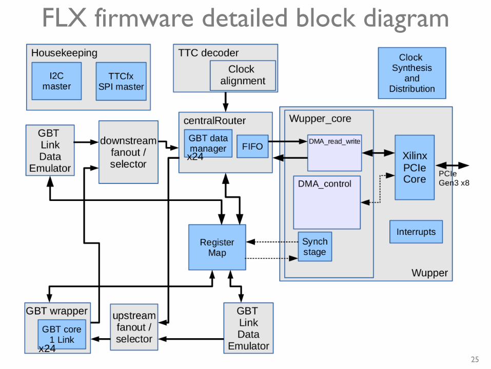
FLX firmware detailed block diagram
25

FELIX firmware: overall clocking
26
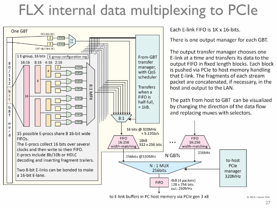
FLX internal data multiplexing to PCIe
27

PCIe throughput
Measurements where done using a simple counter filling the PCIe FIFO
For test purposes only : Single shot DMA transfers
For normal operation: continuous DMA transfer is foreseen
28
One card
Two cards

Tools and tool-flow
Challenge: develop and maintain three platforms Subversion
HDL Works Ease for schematic design entry of HDL blocks
Xilinx Vivado and tcl scripts
Mentor Graphics Questasim and tcl scripts
Code Documentation with Latex and Doxygen
Python scripting and Jinja2 for Register Map to synchronize:
HDL register definition (VHDL)
Application software (C++) and OKS (xml)
Documentation (tex)
Ecosystem of low level software tools for development and debugging
QT based GUIs to control and configure hardware
29
Top Related