
ZyVector Scanned Probe Lithography - Scienta Omicron
4
ZyVector STM Control System for Atomically Precise Lithography www.Scienta Omicron.com Scanned Probe Lithography Scienta Omicron & Zyvex Labs announce collaboraon Scienta Omicron and Zyvex Labs announce a collaboraon to develop and distribute tools for research and manufacturing that require atomic precision. The ZyVector STM Control System from Zyvex Labs turns a Scienta Omicron STM into an atomically-precise scanned- probe lithography tool, and will be distributed world-wide by Scienta Omicron. Scienta Omicron brings together the two leading innovators in Surface Science – the former VG Scienta and Omicron NanoTechnology. This excing new company creates new capabilies for the research community by combining the technology leaders in electron spectroscopy, scanning probe micros- copy and thin film deposion. These capabilies are available in custom tailored systems from one source with sales and service groups located in all major markets around the world. Zyvex LLC pursues the vision to develop Atomically Precise Manufacturing (APM).Recently, Zyvex Labs has developed ZyVector for automated STM Litho- graphy to enable users to create quantum compu- ters and other transformaonal systems that require atomic precision. By pairing it with Scienta Omicron STMs, unmatched lithography will be possible, with much higher reproducibility and throughput, scaling up from research level paerning towards APM. For more details: www.zyvexlabs.com [email protected] Or contact Scienta Omicron, the worldwide distributor: www.scientaomicron.com [email protected] Capabilies ZyVector automates the process of performing Hydrogen Depassivaon Lithography (HDL), using an STM p to remove H atoms from a surface. It can write arbitrary paerns defined in a vector or a bitmap format. Pat- terns can be wrien using a lithography pixel defined by the atomic lace. As well as developing ZyVector as a tool for atomically precise paerning on small scale, researchers at Zyvex Labs are leveraging its capabilies to create nano-funconal devices on the micrometer scale. ZyVector therefore opens up new possibilies to scale up SPM based lithography by seng new standards in reproducibility, automaon, thermal driſt and piezo creep compensaon.
Transcript of ZyVector Scanned Probe Lithography - Scienta Omicron

ZyVectorSTM Control System for Atomically Precise Lithography
www.Scienta Omicron.com
Scanned Probe Lithography Scienta Omicron & Zyvex Labs announce collaborati on
Scienta Omicron and Zyvex Labs announce a collaborati on to develop and distribute tools for research and manufacturing that require atomic precision. The ZyVector STM Control System from Zyvex Labs turns a Scienta Omicron STM into an atomically-precise scanned-probe lithography tool, and will be distributed world-wide by Scienta Omicron.
Scienta Omicron brings together the two leading innovators in Surface Science – the former VG Scienta and Omicron NanoTechnology. This exciti ng new company creates new capabiliti es for the research community by combining the technology leaders in electron spectroscopy, scanning probe micros-copy and thin fi lm depositi on. These capabiliti es are available in custom tailored systems from one source with sales and service groups located in all major markets around the world.
Zyvex LLC pursues the vision to develop Atomically Precise Manufacturing (APM).Recently, Zyvex Labs has developed ZyVector for automated STM Litho-graphy to enable users to create quantum compu-ters and other transformati onal systems that require atomic precision. By pairing it with Scienta Omicron STMs, unmatched lithography will be possible, with much higher reproducibility and throughput, scaling up from research level patt erning towards APM.
For more details: [email protected]
Or contact Scienta Omicron, the worldwide distributor:[email protected]
Capabiliti esZyVector automates the process of performing Hydrogen Depassivati on Lithography (HDL), using an STM ti p to remove H atoms from a surface. It can write arbitrary patt erns defi ned in a vector or a bitmap format. Pat-terns can be writt en using a lithography pixel defi ned by the atomic latti ce. As well as developing ZyVector as a tool for atomically precise patt erning on small scale, researchers at Zyvex Labs are leveraging its capabiliti es to create nano-functi onal devices on the micrometer scale. ZyVector therefore opens up new possibiliti es to scale up SPM based lithography by setti ng new standards in reproducibility, automati on, thermal drift and piezo creep compensati on.
www.Scienta Omicron.com
ZyVectorSTM Control System for Atomically Precise Lithography
ZyVector turns a Scienta Omicron VT STM into an atomically-precise scanned-probe e-beam lithography tool.
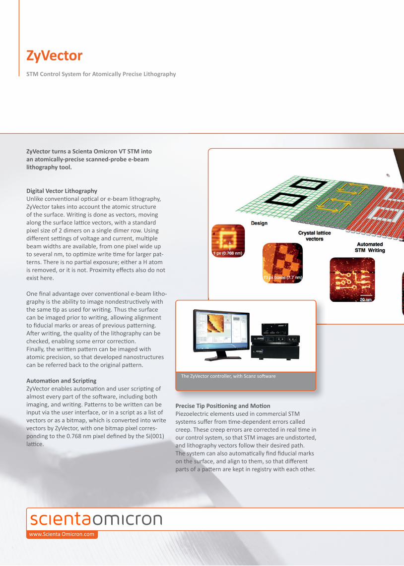
Digital Vector LithographyUnlike conventi onal opti cal or e-beam lithography, ZyVector takes into account the atomic structure of the surface. Writi ng is done as vectors, moving along the surface latti ce vectors, with a standard pixel size of 2 dimers on a single dimer row. Using diff erent setti ngs of voltage and current, multi ple beam widths are available, from one pixel wide up to several nm, to opti mize write ti me for larger pat-terns. There is no parti al exposure; either a H atom is removed, or it is not. Proximity eff ects also do not exist here.
One fi nal advantage over conventi onal e-beam litho-graphy is the ability to image nondestructi vely with the same ti p as used for writi ng. Thus the surface can be imaged prior to writi ng, allowing alignment to fi ducial marks or areas of previous patt erning. Aft er writi ng, the quality of the lithography can be checked, enabling some error correcti on. Finally, the writt en patt ern can be imaged with atomic precision, so that developed nanostructures can be referred back to the original patt ern.
Automati on and Scripti ngZyVector enables automati on and user scripti ng of almost every part of the soft ware, including both imaging, and writi ng. Patt erns to be writt en can be input via the user interface, or in a script as a list of vectors or as a bitmap, which is converted into write vectors by ZyVector, with one bitmap pixel corres-ponding to the 0.768 nm pixel defi ned by the Si(001) latti ce.
Precise Tip Positi oning and Moti on Piezoelectric elements used in commercial STM systems suff er from ti me-dependent errors called creep. These creep errors are corrected in real ti me in our control system, so that STM images are undistorted, and lithography vectors follow their desired path. The system can also automati cally fi nd fi ducial marks on the surface, and align to them, so that diff erent parts of a patt ern are kept in registry with each other.
The ZyVector controller, with Scanz soft ware

www.Scienta Omicron.com
ZyVector at a glance:
● Digital Lithography● Sub-nm pixel● Vector Writi ng, aligned to atomic latti ce● Multi ple beam widths● Built-in Metrology● Automati on and Scripti ng● Automated Imaging, Moving and Writi ng● Vector or Bitmap patt ern input modes● Precise Tip Positi oning and Moti on● Real-ti me Creep Correcti on● Fiducial recogniti on and alignment● Patt ern alignment to latti ce
Technical Specifi cati ons4 fi ne x/y channels (± 135 V)1 fi ne z channel (± 135 V)3 coarse xyz channels (± 200 V)1 ti p bias channel (± 10 V)Current gain control for Omicron pre-ampBias gain control for Omicron pre-amp.Scan Range: up to 9.5 µm on VT STM.
Fits Scienta Omicron VT STM pre-amp and PIC cabling. No modifi cati on of UHV hardware required.
● Local piezo tube calibrati on based on latti ce recogniti on● Latti ce phase recogniti on for precise lithography positi oning● Linear creep correcti on in xy● Two spot size modes:● AP mode(single-dimer-row width)● FE mode multi -nm linewidth, rough edges)
Python-based scripts for test patt erns, creep and latti ce calibrati on, and other basic functi ons are provided. Some example lithography scripts are also included. User-writt en scripts can be run via a menu, or using the command line interface.
A pixel is defi ned as 2 dimers on a dimer row, a 7.68Å square. Write vectors follow the pixel grid, which is laid out across the surface.

ZyVectorSTM Control System for Atomically Precise Lithography
www.Scienta Omicron.com
ASIA PACIFIC
Scienta Omicron - Asia-Pacifi c Sales Offi ce
Oxford Instruments Pte. Ltd.
10 Ubi Crescent #04-81, Ubi Techpark,
Lobby E, Singapore, 408564
Phone: +65 633 76848
Mail: [email protected]
AUSTRALIA:
Scitek total vacuum soluti ons
Phone: 1800 023 467
Mail: [email protected]
CHINA:
ScientaOmicron Beijing Sales & Service
Offi ce
87 West 3rd Ring North Road
Beijing, 100089 Haidan District
China
Phone: +86 10-8882-4423
Mail: [email protected]
Mail: [email protected]
FRANCE
ScientaOmicron EURL
France & Southern Europe & North Africa
Sales Offi ce
(Omicron NanoTechnology E.U.R.L.)
Le plan d‘Aigues, RN 7,
13760 St.-Cannat
Phone: +33 442 50 68 64
Mail: [email protected]
INDIA
Mack Internati onal
Phone: +91 22 2285 5261
Mail: [email protected]
Mail: [email protected]
ITALY
LOT-QuantumDesign s.r.l.
Phone: +39 06 5004 204
Mail: [email protected]
JAPAN
Scienta Omicron, Inc.
Tonami Omori Building
6-16-4 Minami-Oi Shinagawa-ku,
Tokyo 140-0013, JP
Phone: +81-3-6404-9133
Mail: [email protected]
Mail: [email protected]
POLAND
APVacuum Sp. z.o.o.
Phone: +48 61 65 63 530
Mail: offi [email protected]
ROMANIA
Nitech S.R.L.
Phone: +40 21 668 6819
Mail: offi [email protected]
RUSSIA
IMC-Group Ltd.
Phone: +7 (495) 374 0401
Mail: [email protected]
SAUDI ARABIA
Naizak Global Engineering Systems
Phone: +966 1 4161161/ 4633635/
Mail: [email protected]
SINGAPORE
Agent: Portsdown Scienti fi c Pte. Ltd.
Phone: +65 93821401
Mail: [email protected]
SOUTH AMERICA
Quantum Design America do Sul Ltda.
Phone: +55 (19) 3212-0230
Mail: [email protected]
SOUTH KOREA
Korea Sales & Service Offi ce
Phone: +82 2 2047 6466
Mail: [email protected]
SPAIN
TECNOVAC TECHNOLOGIA VACIO S.L.
Phone: +34 91 804 11 34
Mail: [email protected]
SWEDEN
ROWACO AB
Phone: +46 13 138 010
Mail: kristi [email protected]
TAIWAN
Omega Scienti fi c Taiwan Ltd.
Phone: +886 2 2793 0033
Mail: [email protected]
TURKEY
Nanomanyeti k Bilimsel Cihazlar Ltd.
Phone: +90 (312) 299 21 71
Mail: sales@nanomagneti cs-inst.com
USA
Scienta Omicron, Inc.
North American Headquarters
240 St. Paul Street, , Suite 301
Denver, CO 80206, USA
Phone: +1 720 350 5000
Mail: [email protected]
Eastern Regional Sales Offi ce
4150 Washington Road, Suite 204
McMurray, PA 15317, USA
Phone: +1 724 942 9821
Mail: [email protected]
West Coast Regional Sales Offi ce
Los Angeles, CA 90025, USA
Phone: +1 310 331 8402
Mail: [email protected]
South & Midwest Regional Sales Offi ce
Davidson, NC 28036, USA
Phone: +1 720 350 5000 ext. 413
Mail: [email protected]
North American Service Offi ce
14850 Scenic Heights Road, Suite 140
Eden Prairie, MN 55344, USA
Phone: +1 952 345 5243
Mail: [email protected]
GermanyLimburger Str. 7565232 TaunussteinGERMANY+49 6128 987 – [email protected]
SwedenP.O. Box 15120, SE-750 15, UPPSALASWEDEN +46 (0)18 480 58 [email protected]
Two XPS samples on a sample
holder - one masked with Au foil.
Scienta Omicron VT STMScienta Omicron VT STM


![1 3 c arXiv:2010.05308v1 [cond-mat.supr-con] 11 Oct 20202 II. EXPERIMENTAL METHODS We grew FeSe lms on TiO 2-terminated STO (001) substrates with atomically at steps in a Scienta Omicron](https://static.fdocuments.net/doc/165x107/60ae971d2942273baa699b00/1-3-c-arxiv201005308v1-cond-matsupr-con-11-oct-2020-2-ii-experimental-methods.jpg)


