
Zot Printed Circuit Division
88
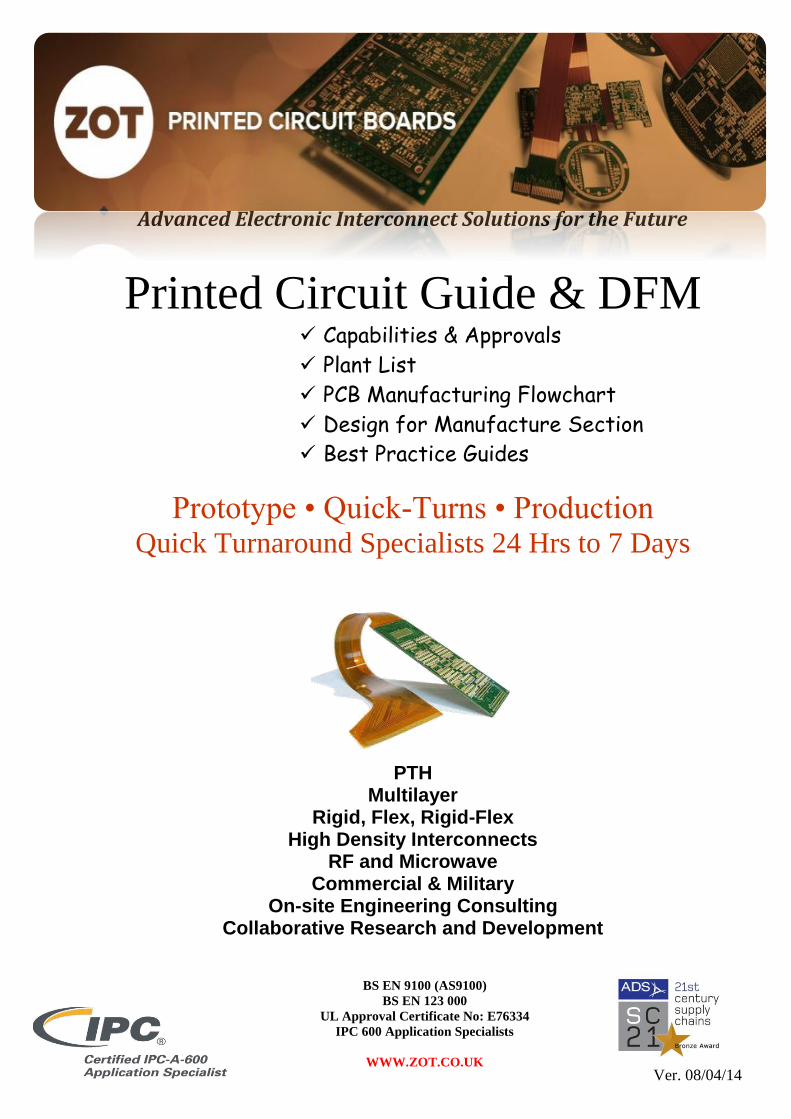
Ver. 08/04/14 Zot Printed Circuit Division Advanced Electronic Interconnect Solutions for the Future Printed Circuit Guide & DFM Capabilities & Approvals Plant List PCB Manufacturing Flowchart Design for Manufacture Section Best Practice Guides Prototype • Quick-Turns • Production Quick Turnaround Specialists 24 Hrs to 7 Days PTH Multilayer Rigid, Flex, Rigid-Flex High Density Interconnects RF and Microwave Commercial & Military On-site Engineering Consulting Collaborative Research and Development BS EN 9100 (AS9100) BS EN 123 000 UL Approval Certificate No: E76334 IPC 600 Application Specialists WWW.ZOT.CO.UK
-
Upload
duongthien -
Category
Documents
-
view
227 -
download
2
Transcript of Zot Printed Circuit Division
Ver. 08/04/14
Zot
Printed Circuit Division Advanced Electronic Interconnect Solutions for the Future
Printed Circuit Guide & DFM Capabilities & Approvals
Plant List
PCB Manufacturing Flowchart
Design for Manufacture Section
Best Practice Guides
Prototype • Quick-Turns • Production Quick Turnaround Specialists 24 Hrs to 7 Days
PTH
Multilayer Rigid, Flex, Rigid-Flex
High Density Interconnects RF and Microwave
Commercial & Military On-site Engineering Consulting
Collaborative Research and Development
BS EN 9100 (AS9100)
BS EN 123 000
UL Approval Certificate No: E76334
IPC 600 Application Specialists
WWW.ZOT.CO.UK
Zot Printed Circuit Guide
www.zot.co.uk 2
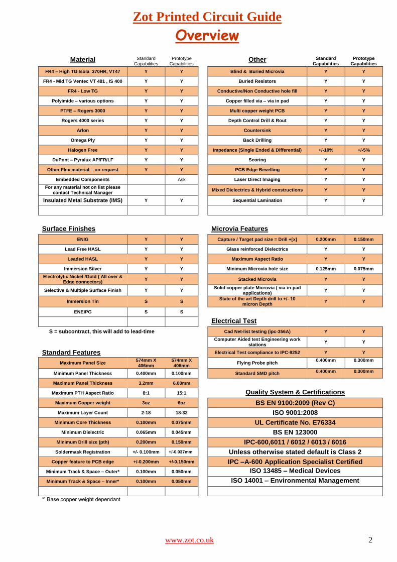
Overview
Material Standard Capabilities
Prototype Capabilities
Other Standard Capabilities
Prototype Capabilities
FR4 – High TG Isola 370HR, VT47 Y Y Blind & Buried Microvia Y Y
FR4 - Mid TG Ventec VT 481 , IS 400 Y Y Buried Resistors Y Y
FR4 - Low TG Y Y Conductive/Non Conductive hole fill Y Y
Polyimide – various options Y Y Copper filled via – via in pad Y Y
PTFE – Rogers 3000 Y Y Multi copper weight PCB Y Y
Rogers 4000 series Y Y Depth Control Drill & Rout Y Y
Arlon Y Y Countersink Y Y
Omega Ply Y Y Back Drilling Y Y
Halogen Free Y Y Impedance (Single Ended & Differential) +/-10% +/-5%
DuPont – Pyralux AP/FR/LF Y Y Scoring Y Y
Other Flex material – on request Y Y PCB Edge Bevelling Y Y
Embedded Components Ask Laser Direct Imaging Y Y For any material not on list please
contact Technical Manager Mixed Dielectrics & Hybrid constructions Y Y
Insulated Metal Substrate (IMS) Y Y Sequential Lamination Y Y
Surface Finishes Microvia Features
ENIG Y Y Capture / Target pad size = Drill +[x] 0.200mm 0.150mm
Lead Free HASL Y Y Glass reinforced Dielectrics Y Y
Leaded HASL Y Y Maximum Aspect Ratio Y Y
Immersion Silver Y Y Minimum Microvia hole size 0.125mm 0.075mm Electrolytic Nickel /Gold ( All over &
Edge connectors) Y Y
Stacked Microvia Y Y
Selective & Multiple Surface Finish Y Y Solid copper plate Microvia ( via-in-pad applications)
Y Y
Immersion Tin S S State of the art Depth drill to +/- 10 micron Depth
Y Y
ENEIPG S S
Electrical Test
S = subcontract, this will add to lead-time Cad Net-list testing (ipc-356A) Y Y
Computer Aided test Engineering work stations
Y Y
Standard Features Electrical Test compliance to IPC-9252 Y Y
Maximum Panel Size 574mm X 406mm
574mm X 406mm
Flying Probe pitch
0.400mm 0.300mm
Minimum Panel Thickness 0.400mm 0.100mm Standard SMD pitch 0.400mm 0.300mm
Maximum Panel Thickness 3.2mm 6.00mm
Maximum PTH Aspect Ratio 8:1 15:1 Quality System & Certifications
Maximum Copper weight 3oz 6oz BS EN 9100:2009 (Rev C)
Maximum Layer Count 2-18 18-32 ISO 9001:2008
Minimum Core Thickness 0.100mm 0.075mm UL Certificate No. E76334
Minimum Dielectric 0.065mm 0.045mm BS EN 123000
Minimum Drill size (pth) 0.200mm 0.150mm IPC-600,6011 / 6012 / 6013 / 6016
Soldermask Registration +/- 0.100mm +/-0.037mm Unless otherwise stated default is Class 2
Copper feature to PCB edge +/-0.200mm +/-0.150mm IPC –A-600 Application Specialist Certified
Minimum Track & Space – Outer* 0.100mm 0.050mm ISO 13485 – Medical Devices
Minimum Track & Space – Inner* 0.100mm 0.050mm ISO 14001 – Environmental Management
*’ Base copper weight dependant
Zot Printed Circuit Guide
www.zot.co.uk 3
Introduction
About Zot We were established in 1975, and service the needs of all sectors of the worldwide electronics industry. We continue to build on our industry relationships through our policy of continual investment year-on-year in the latest PCB technologies, and are recognised as one of the leading pcb manufacturing companies in the Europe. For an overview of the company please visit : www.zot.co.uk
WHAT CAN THE PCB DIVISION DO? We specialise in producing small to medium batch quantities from 24 hour turnaround. Standard turnaround is typically 10 to 12 working days. We understand the need for maintaining our customer’s competitiveness, therefore we also offer offshore volume supply options, utilising our experience in monitoring and testing to ensure that offshore enjoys the same quality systems as in-house production. Whether the design is plated through hole, controlled impedance, backplanes, bonded heatsinks, multilayer to 24 layers+, microvia, buried/blind via, or even flexi-rigid, we have the experience and ability to produce your design. Our manufacturing processes use state of the art pcb manufacturing equipment such as Laser Direct Imaging, Soft Touch flying probe testing, 4 slot innerlayer tooling and environmentally friendly direct legend printing. These processes and others, allow us to hold very tight tolerances.
What Makes The Pcb Division Different?
Our PCB Division not only enjoys over 30 years of experience in the small to medium scale development and production of PCBs, but also maintains a client portfolio which stands as testament to the company's long-term reliability. In many cases our clients who have been with the business for over a decade. We believe this is due to the company's efforts to recognise and meet the particular needs of each customer. Quality is key to the PCB division but not at the expense of price. We pride ourselves on the ability to deliver on time, to a competitive budget, with quality that will encourage repeat business.
Front End Engineering Ability
We have a wealth of front end engineering ability, most of our Front End Engineers, have been in the Printed Circuit Industry for 20 years. The combined front end experience of our tooling engineers is over 150 years, this with the combination of sophisticated computer systems ensures we have the right knowledge to engineer your design for manufacturability, and help design quality in. All designs are fully design rule checked, and verified to net lists during engineering and subsequent automatic optical inspection and electrical testing of your product. Our tooling department is manned 24 hours a day. We have 2 tooling sites, 1 in our main site in Musselburgh, and another site in the West of Scotland, these all work as virtual offices.
Production Facilities
Our production facility is well manned with a highly skilled and knowledgeable workforce, and our equipment purchasing strategies ensure that our state of the art production facility is well equipped with the latest in pcb manufacturing technologies, such as imaging processes like Laser Direct Imaging and soft touch probe testing, and with our fundamental commitment to quality, delivery and service, with continuous improvement programmes utilising a variety of process & quality control tools, backed up with our fully equipped laboratory, ensures our customers of an outstanding service from a world class manufacturer. All processes are controlled by various quality methods, including Cp & Cpk, preventative maintenance schedules, critical characteristics, every possible variable & attribute is monitored and controlled. This is also backed up with a well equipped Laboratory, covered 24 hours a day.
Zot Printed Circuit Guide
www.zot.co.uk 4
Electrolytic Gold
Electrical Test
Prt Peelable
Despatch to Customer
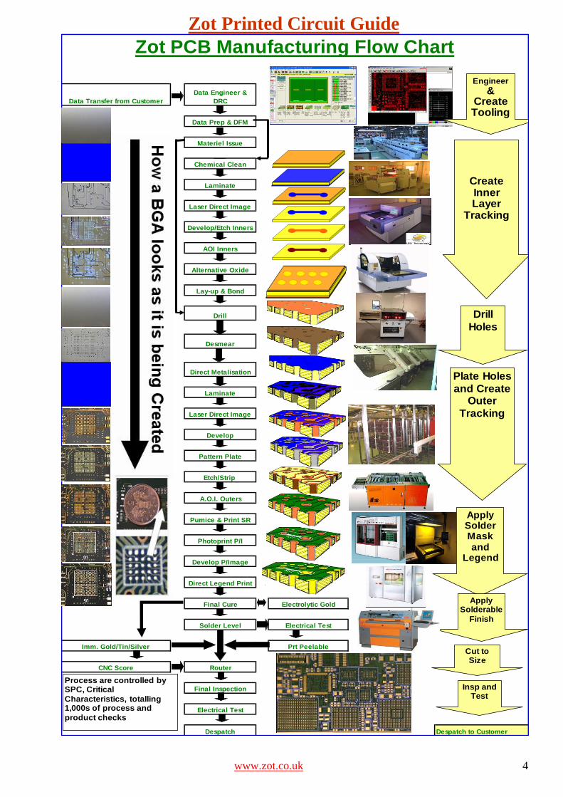
Zot PCB Manufacturing Flow Chart
Data Transfer from Customer
Data Engineer &
DRC
Imm. Gold/Tin/Silver
Data Prep & DFM
Materiel Issue
Chemical Clean
Laminate
Lay-up & Bond
Drill
Direct Metalisation
Laminate
Laser Direct Image
Develop
Desmear
Laser Direct Image
Develop/Etch Inners
AOI Inners
Alternative Oxide
Photoprint P/I
Develop P/Image
Direct Legend Print
Final Cure
Pattern Plate
Etch/Strip
A.O.I. Outers
Pumice & Print SR
Solder Level
Router
Final Inspection
Despatch
Electrical Test
CNC Score
Engineer
& Create Tooling
Create InnerLayer
Tracking
Drill
Holes
Plate Holes
and CreateOuter
Tracking
Apply SolderMaskand
Legend
Apply Solderable
Finish
Cut to Size
Insp and Test
Process are controlled by SPC, Critical
Characteristics, totalling 1,000s of process and
product checks
Zot Printed Circuit Guide
www.zot.co.uk 5
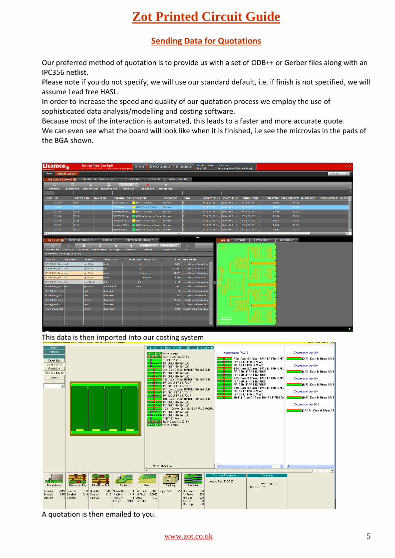
Sending Data for Quotations Our preferred method of quotation is to provide us with a set of ODB++ or Gerber files along with an IPC356 netlist. Please note if you do not specify, we will use our standard default, i.e. if finish is not specified, we will assume Lead free HASL. In order to increase the speed and quality of our quotation process we employ the use of sophisticated data analysis/modelling and costing software. Because most of the interaction is automated, this leads to a faster and more accurate quote. We can even see what the board will look like when it is finished, i.e see the microvias in the pads of the BGA shown.
This data is then imported into our costing system
A quotation is then emailed to you.
Zot Printed Circuit Guide
www.zot.co.uk 6
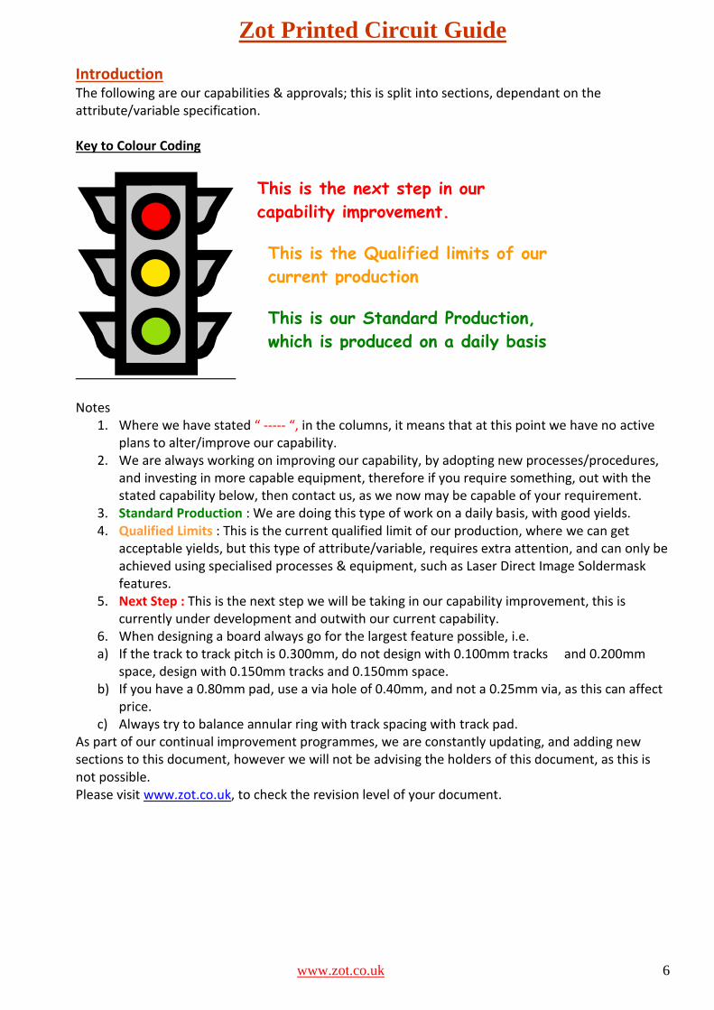
Introduction The following are our capabilities & approvals; this is split into sections, dependant on the attribute/variable specification. Key to Colour Coding
Notes
1. Where we have stated “ ----- “, in the columns, it means that at this point we have no active plans to alter/improve our capability.
2. We are always working on improving our capability, by adopting new processes/procedures, and investing in more capable equipment, therefore if you require something, out with the stated capability below, then contact us, as we now may be capable of your requirement.
3. Standard Production : We are doing this type of work on a daily basis, with good yields. 4. Qualified Limits : This is the current qualified limit of our production, where we can get
acceptable yields, but this type of attribute/variable, requires extra attention, and can only be achieved using specialised processes & equipment, such as Laser Direct Image Soldermask features.
5. Next Step : This is the next step we will be taking in our capability improvement, this is currently under development and outwith our current capability.
6. When designing a board always go for the largest feature possible, i.e. a) If the track to track pitch is 0.300mm, do not design with 0.100mm tracks and 0.200mm
space, design with 0.150mm tracks and 0.150mm space. b) If you have a 0.80mm pad, use a via hole of 0.40mm, and not a 0.25mm via, as this can affect
price. c) Always try to balance annular ring with track spacing with track pad.
As part of our continual improvement programmes, we are constantly updating, and adding new sections to this document, however we will not be advising the holders of this document, as this is not possible. Please visit www.zot.co.uk, to check the revision level of your document.
This is the next step in our
capability improvement.
programme This is the Qualified limits of our
current production
This is our Standard Production,
which is produced on a daily basis
Zot Printed Circuit Guide
www.zot.co.uk 7
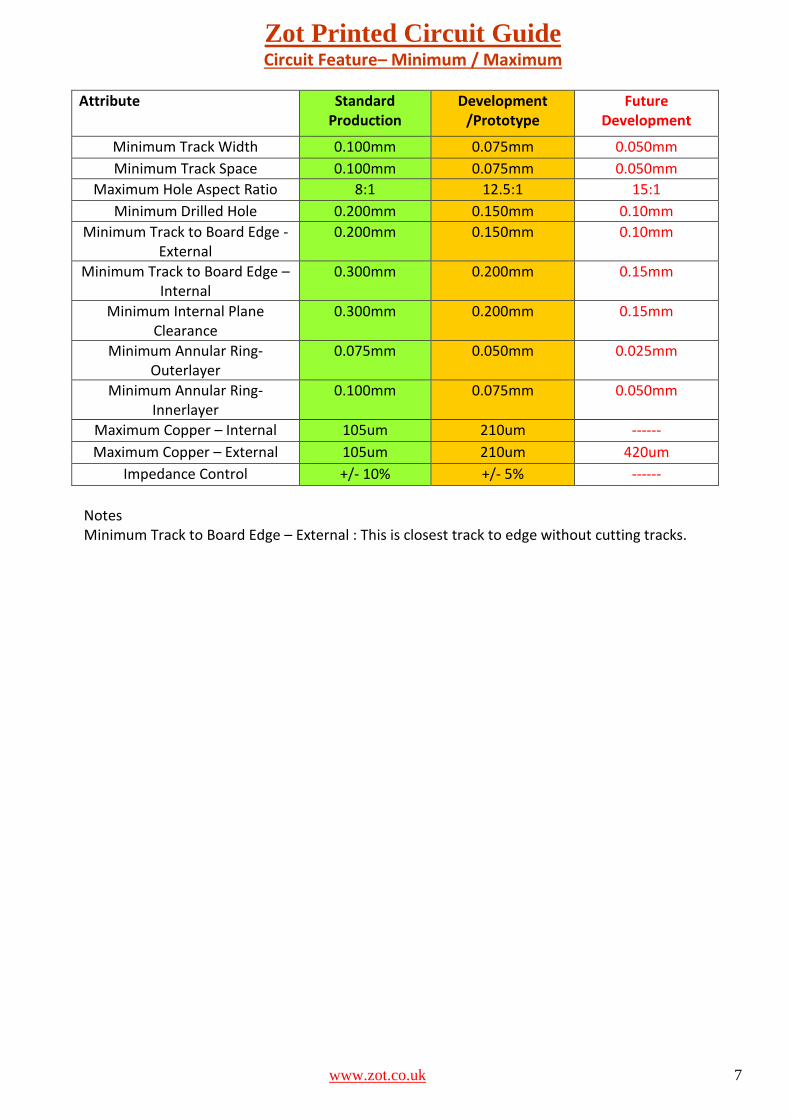
Circuit Feature– Minimum / Maximum
Attribute Standard Production
Development /Prototype
Future Development
Minimum Track Width 0.100mm 0.075mm 0.050mm
Minimum Track Space 0.100mm 0.075mm 0.050mm
Maximum Hole Aspect Ratio 8:1 12.5:1 15:1
Minimum Drilled Hole 0.200mm 0.150mm 0.10mm
Minimum Track to Board Edge - External
0.200mm 0.150mm 0.10mm
Minimum Track to Board Edge – Internal
0.300mm 0.200mm 0.15mm
Minimum Internal Plane Clearance
0.300mm 0.200mm 0.15mm
Minimum Annular Ring- Outerlayer
0.075mm 0.050mm 0.025mm
Minimum Annular Ring- Innerlayer
0.100mm 0.075mm 0.050mm
Maximum Copper – Internal 105um 210um ------
Maximum Copper – External 105um 210um 420um
Impedance Control +/- 10% +/- 5% ------
Notes Minimum Track to Board Edge – External : This is closest track to edge without cutting tracks.
Zot Printed Circuit Guide
www.zot.co.uk 8
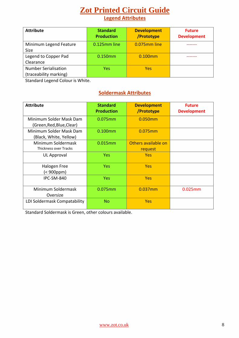
Legend Attributes
Attribute Standard Production
Development /Prototype
Future Development
Minimum Legend Feature Size
0.125mm line 0.075mm line -------
Legend to Copper Pad Clearance
0.150mm 0.100mm -------
Number Serialisation (traceability marking)
Yes Yes
Standard Legend Colour is White.
Soldermask Attributes
Attribute Standard Production
Development /Prototype
Future Development
Minimum Solder Mask Dam (Green,Red,Blue,Clear)
0.075mm 0.050mm
Minimum Solder Mask Dam (Black, White, Yellow)
0.100mm 0.075mm
Minimum Soldermask Thickness over Tracks
0.015mm Others available on request
UL Approval Yes Yes
Halogen Free (< 900ppm)
Yes Yes
IPC-SM-840 Yes Yes
Minimum Soldermask Oversize
0.075mm 0.037mm 0.025mm
LDI Soldermask Compatability No Yes
Standard Soldermask is Green, other colours available.
Zot Printed Circuit Guide
www.zot.co.uk 9
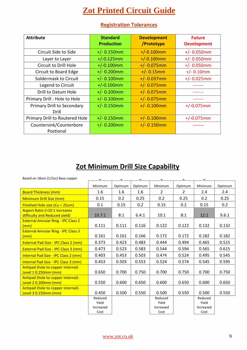
Registration Tolerances
Attribute Standard Production
Development /Prototype
Future Development
Circuit Side to Side +/- 0.150mm +/-0.100mm +/- 0.050mm
Layer to Layer +/-0.125mm +/-0.100mm +/- 0.050mm
Circuit to Drill Hole +/-0.100mm +/- 0.075mm +/- 0.050mm
Circuit to Board Edge +/- 0.200mm +/- 0.15mm +/- 0.10mm
Soldermask to Circuit +/- 0.100mm +/- 0.037mm +/- 0.025mm
Legend to Circuit +/-0.100mm +/- 0.075mm -------
Drill to Datum Hole +/- 0.100mm +/- 0.075mm -------
Primary Drill : Hole to Hole +/- 0.100mm +/- 0.075mm -------
Primary Drill to Secondary Drill
+/- 0.150mm +/- 0.100mm +/-0.075mm
Primary Drill to Routered Hole +/- 0.150mm +/- 0.100mm +/-0.075mm
Countersink/Counterbore Postional
+/- 0.200mm +/- 0.150mm -------
Zot Minimum Drill Size Capability
Based on 18um (1/2oz) Base copper
Minimum Optimum Optimum Minimum Optimum Minimum Optimum
Board Thickness (mm) 1.6 1.6 1.6 2 2 2.4 2.4
Minimum Drill Size (mm) 0.15 0.2 0.25 0.2 0.25 0.2 0.25
Finished Hole size (Cu = 25um) 0.1 0.15 0.2 0.15 0.2 0.15 0.2 Aspect Ratio (>10:1 increases difficulty and Reduced yield) 10.7:1 8:1 6.4:1 10:1 8:1 12:1 9.6:1 External Annular Ring - IPC Class 2 (mm) 0.111 0.111 0.116 0.122 0.122 0.132 0.132 External Annular Ring - IPC Class 3 (mm) 0.161 0.161 0.166 0.172 0.172 0.182 0.182
External Pad Size - IPC Class 2 (mm) 0.373 0.423 0.483 0.444 0.494 0.465 0.515
External Pad Size - IPC Class 3 (mm) 0.473 0.523 0.583 0.544 0.594 0.565 0.615
Internal Pad Size - IPC Class 2 (mm) 0.403 0.453 0.503 0.474 0.524 0.495 0.545
Internal Pad Size - IPC Class 3 (mm) 0.453 0.503 0.553 0.524 0.574 0.545 0.595 Antipad (hole to copper internal)- Level 1 0.250mm (mm) 0.650 0.700 0.750 0.700 0.750 0.700 0.750 Antipad (hole to copper internal)- Level 2 0.200mm (mm) 0.550 0.600 0.650 0.600 0.650 0.600 0.650 Antipad (hole to copper internal)- Level 3 0.150mm (mm) 0.450 0.500 0.550 0.500 0.550 0.500 0.550
Reduced Yield
Reduced Yield
Reduced Yield
Increased Cost
Increased Cost
Increased Cost
Zot Printed Circuit Guide
www.zot.co.uk 10
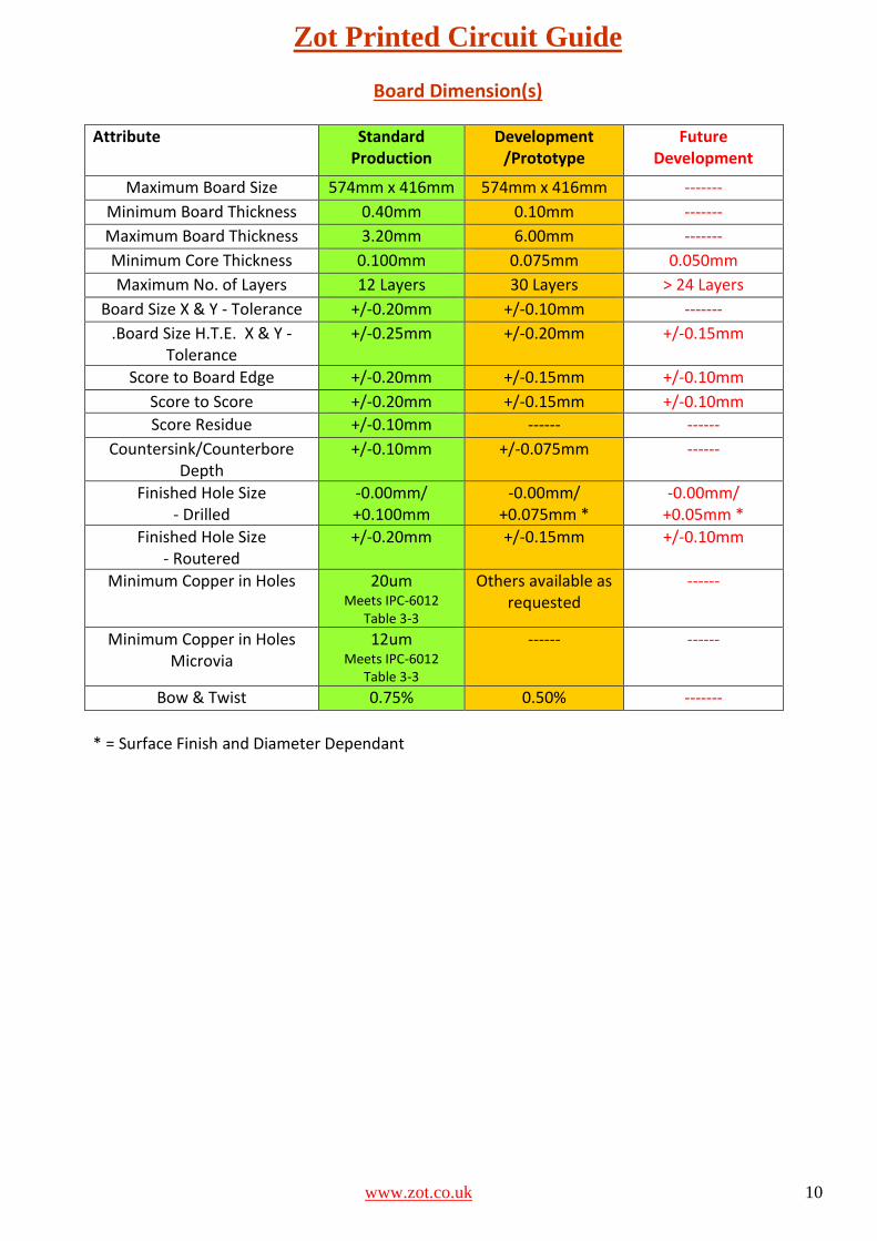
Board Dimension(s)
Attribute Standard Production
Development /Prototype
Future Development
Maximum Board Size 574mm x 416mm 574mm x 416mm -------
Minimum Board Thickness 0.40mm 0.10mm -------
Maximum Board Thickness 3.20mm 6.00mm -------
Minimum Core Thickness 0.100mm 0.075mm 0.050mm
Maximum No. of Layers 12 Layers 30 Layers > 24 Layers
Board Size X & Y - Tolerance +/-0.20mm +/-0.10mm -------
.Board Size H.T.E. X & Y - Tolerance
+/-0.25mm +/-0.20mm +/-0.15mm
Score to Board Edge +/-0.20mm +/-0.15mm +/-0.10mm
Score to Score +/-0.20mm +/-0.15mm +/-0.10mm
Score Residue +/-0.10mm ------ ------
Countersink/Counterbore Depth
+/-0.10mm +/-0.075mm ------
Finished Hole Size - Drilled
-0.00mm/ +0.100mm
-0.00mm/ +0.075mm *
-0.00mm/ +0.05mm *
Finished Hole Size - Routered
+/-0.20mm +/-0.15mm +/-0.10mm
Minimum Copper in Holes 20um Meets IPC-6012
Table 3-3
Others available as requested
------
Minimum Copper in Holes Microvia
12um Meets IPC-6012
Table 3-3
------ ------
Bow & Twist 0.75% 0.50% -------
* = Surface Finish and Diameter Dependant
Zot Printed Circuit Guide
www.zot.co.uk 11
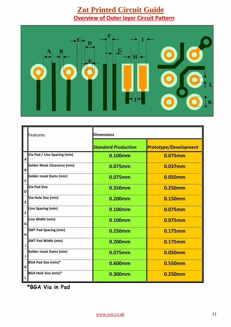
Overview of Outer layer Circuit Pattern
Features Dimensions
Standard Production Prototype/Development
A Via Pad / Line Spacing (min) 0.100mm 0.075mm
B Solder Mask Clearance (min) 0.075mm 0.037mm
C Solder mask Dams (min) 0.075mm 0.050mm
D Via Pad Size 0.350mm 0.250mm
E Via Hole Size (min) 0.200mm 0.150mm
F Line Spacing (min) 0.100mm 0.075mm
G Line Width (min) 0.100mm 0.075mm
H SMT Pad Spacing (min) 0.250mm 0.175mm
I SMT Pad Width (min) 0.200mm 0.175mm
J Solder mask Dams (min) 0.075mm 0.050mm
K BGA Pad Size (min)* 0.600mm 0.550mm
L BGA Hole Size (min)* 0.300mm 0.250mm
*BGA Via in Pad
A B
C D
F
G
H
I
J
E
K
L
B A
Zot Printed Circuit Guide
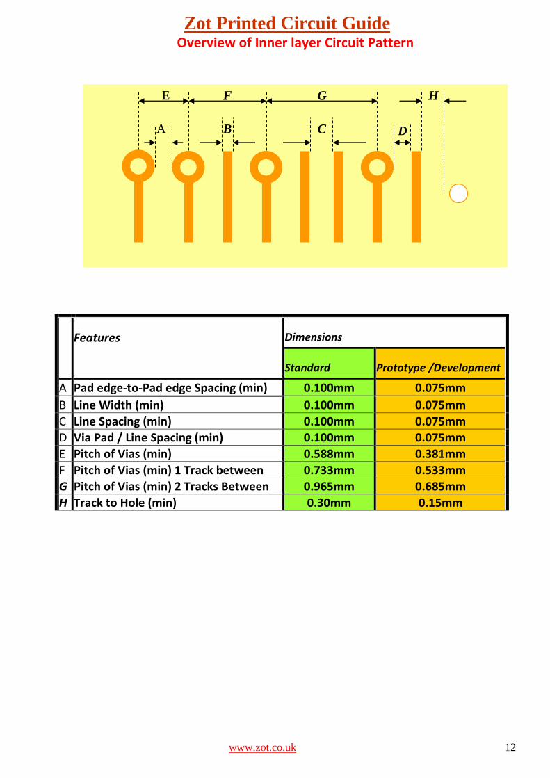
www.zot.co.uk 12
Overview of Inner layer Circuit Pattern
Features Dimensions
Standard Prototype /Development
A Pad edge-to-Pad edge Spacing (min) 0.100mm 0.075mm
B Line Width (min) 0.100mm 0.075mm
C Line Spacing (min) 0.100mm 0.075mm D Via Pad / Line Spacing (min) 0.100mm 0.075mm
E Pitch of Vias (min) 0.588mm 0.381mm
F Pitch of Vias (min) 1 Track between 0.733mm 0.533mm G Pitch of Vias (min) 2 Tracks Between 0.965mm 0.685mm
H Track to Hole (min) 0.30mm 0.15mm
E
A
F
B
G
C D
H
Zot Printed Circuit Guide
www.zot.co.uk 13
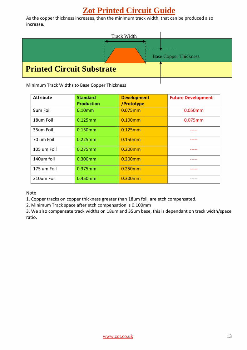
As the copper thickness increases, then the minimum track width, that can be produced also increase. Minimum Track Widths to Base Copper Thickness
Attribute Standard Production
Development /Prototype
Future Development
9um Foil 0.10mm 0.075mm 0.050mm
18um Foil 0.125mm 0.100mm 0.075mm
35um Foil 0.150mm 0.125mm -----
70 um Foil 0.225mm 0.150mm -----
105 um Foil 0.275mm 0.200mm -----
140um foil 0.300mm 0.200mm -----
175 um Foil 0.375mm 0.250mm -----
210um Foil 0.450mm 0.300mm -----
Note 1. Copper tracks on copper thickness greater than 18um foil, are etch compensated. 2. Minimum Track space after etch compensation is 0.100mm 3. We also compensate track widths on 18um and 35um base, this is dependant on track width/space ratio.
Printed Circuit Substrate
Track Width
Base Copper Thickness
Zot Printed Circuit Guide
www.zot.co.uk 14
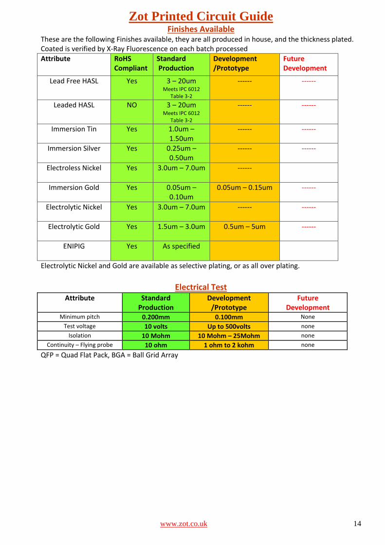
Finishes Available
These are the following Finishes available, they are all produced in house, and the thickness plated. Coated is verified by X-Ray Fluorescence on each batch processed
Attribute RoHS Compliant
Standard Production
Development /Prototype
Future Development
Lead Free HASL Yes 3 – 20um Meets IPC 6012
Table 3-2
------ ------
Leaded HASL NO 3 – 20um Meets IPC 6012
Table 3-2
------ ------
Immersion Tin
Yes 1.0um – 1.50um
------ ------
Immersion Silver Yes 0.25um – 0.50um
------ ------
Electroless Nickel Yes 3.0um – 7.0um ------
Immersion Gold Yes 0.05um – 0.10um
0.05um – 0.15um ------
Electrolytic Nickel Yes 3.0um – 7.0um ------ ------
Electrolytic Gold Yes 1.5um – 3.0um 0.5um – 5um ------
ENIPIG Yes As specified
Electrolytic Nickel and Gold are available as selective plating, or as all over plating.
Electrical Test
Attribute Standard Production
Development /Prototype
Future Development
Minimum pitch 0.200mm 0.100mm None Test voltage 10 volts Up to 500volts none
Isolation 10 Mohm 10 Mohm – 25Mohm none Continuity – Flying probe 10 ohm 1 ohm to 2 kohm none
QFP = Quad Flat Pack, BGA = Ball Grid Array
Zot Printed Circuit Guide
www.zot.co.uk 15
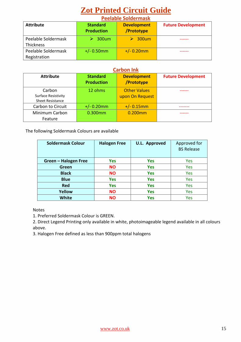
Peelable Soldermask
Attribute Standard Production
Development /Prototype
Future Development
Peelable Soldermask Thickness
300um 300um ------
Peelable Soldermask Registration
+/- 0.50mm +/- 0.20mm ------
Carbon Ink Attribute Standard
Production Development
/Prototype Future Development
Carbon Surface Resistivity Sheet Resistance
12 ohms Other Values upon On Request
------
Carbon to Circuit +/- 0.20mm +/- 0.15mm -------
Minimum Carbon Feature
0.300mm 0.200mm ------
The following Soldermask Colours are available
Soldermask Colour Halogen Free U.L. Approved Approved for BS Release
Green – Halogen Free Yes Yes Yes
Green NO Yes Yes
Black NO Yes Yes
Blue Yes Yes Yes
Red Yes Yes Yes
Yellow NO Yes Yes
White NO Yes Yes
Notes 1. Preferred Soldermask Colour is GREEN. 2. Direct Legend Printing only available in white, photoimageable legend available in all colours above. 3. Halogen Free defined as less than 900ppm total halogens
Zot Printed Circuit Guide
www.zot.co.uk 16
Laminate The following Table represents the laminates which we can manufacture, in the respective board product types, available in single sided, pth and multilayer. If the laminate you require is not listed below, please contact our technical department for more information.
FR4 Materials Dicy Cured Fr4 : SN-L41, De117, N4000-6, PCL 240, PCL370, FR4-ML, FR4-RD, FR4, De104 De104i, 104-TS, 1755C (R1650C P/P), IS410, VT-481,370HR, N4000-29, R1566 (R1551P/P), VT-47TC Fr4 H/Free = R1566, De156 All Fr4 Type Materials
Other PCB Laminates Polyimide: N7000 series, P95,96,97, VT-901 Arlon Diclad Aramid PTFE Laminates Metal Backed Laminates
Rogers type Laminates R03000 Series PTFE Ceramic R04000 Series RT/duroid® 5000 PTFE Glass Fibre RT/duroid® 6000 PTFE Ceramic TMM® Hydrocarbon Ceramic ULTRALAM® 2000 PTFE Woven Glass ULTRALAM® 3000 Liquid Crystalline
Flexible Materials Dupont Espanex If you require a laminate that is not listed above, please contact us.
Zot Printed Circuit Guide
www.zot.co.uk 17
Quality Approvals Quality System Approval Quality System : BS EN 9100 (AS9100) British Standards Product Approval BS EN 123 000 BS EN 123 100 BS EN 123 200 BS EN 123 300 Assessment Level C Registration No: M1052 IECQ-CECC Certificate No: E086/CA Underwiters Laboratory Approval UL Approval Certificate No: E73364 ISO 13485 – Medical devices ISO 14001 - Environmental IPC Certification IPC-A-600 Application Specialist
Notes
1. Copies of BS Release certificates and Scope are available upon request. Limitation of Approvals - The following is the scope of our BS EN123000 Approval
BS EN 123000 Attribute/Variable Approved for BS Release
Hot Air Solder Level - Leaded Yes
Hot Air Solder Level – Lead Free HASL Yes
Immersion Silver Yes
Immersion Tin No
Electroless Nickel, Imm.Gold Yes
Electrolytic Gold (2.5um gold on 5um Nickel – Contacts Only )
Yes
Photoimageable Soldermask Yes
Photoimageable Legend Yes
Direct Legend Print Yes
Peelable Soldermask Yes
Minimum Track Width 0.100mm
Minimum Space 0.100mm
Minimum Hole Size 0.20mm
Maximum No. of Layers 24
Aspect Ratio 12.5:1
FR4 Laminate Family Yes
Board Size 584mm x 432mm
Zot Printed Circuit Guide
www.zot.co.uk 18
Underwriters Approval ( UL Approval ) Limitations : File no: E76334(M) UL Approval – Finishes & Coatings Approved for
UL Release
Lead free HASL Yes
Leaded HASL Yes
Immersion Tin Yes
Immersion Silver Yes
Electroless Nickel / Immersion Gold Yes
Electrolytic Gold Yes
Soldermask – All Colours Yes
Legend Yes
Carbon No
Peelable Soldermask Yes
UL Approval – Conductor Pattern Limit
Maximum Operating Temp 130c
UL 796 (DSR ) All
UL Flame Class V-0
Minimum Edge Conductor 0.050mm
Minimum Conductor 0.150mm
Maximum Unpierced Area ( Outer ) (<105um Base Copper )
150mm Diameter
Maximum Unpierced Area (Outer ) (>105um Base Copper )
114mm Diameter
Maximum Unpierced Area ( Inner ) 210um Diameter
Minimum Core Thickness 0.100mm
Minimum Board Thickness 0.80mm
Maximum Copper Weight 210 micron
UL Approval – Board Types/Materials Approved for UL Release
FR4 Yes
Sequential Multilayer Build Yes
Polyimide Yes – UL 94V-1
Rogers/Getek/Aramid No
Flexibles & Flexi-rigids No
General Specification Unless otherwise stated we work to I.P.C. 600 ( Latest Revision )Class 2, and I.P.C. 6012. Certified IPC 600 Application Specialist
Zot Printed Circuit Guide
www.zot.co.uk 19
Zot Flexible
Why use Flex & Flex-Rigid Technology? Flex& flex-Rigid PCB’s have been widely used in a variety of applications and markets for many years where space and size is critical to its function as an interconnect either between connectors or to other rigid PCB’s. At Zot Printed Circuits we are seeing more and more customers migrate to flex& flex-Rigids due to the benefits of its construction, some examples as follows: •3d interconnect •1 part component (as opposed to multiple rigid pcb’s and wiring looms) •increased reliability •space saver •reduced labour costs at assy •fully tested as a 1pc component
FLEX CIRCUIT TYPES FOR OPTIMAL INTERCONNECTION Different types of flex circuits offer different advantages. Some offer lower cost, while others increase functionality. Zot Printed
Circuit has invested heavily in advanced manufacturing equipment and Engineer/Operator training to meet the needs of this
market. Learn more about the circuit types available for your application below:
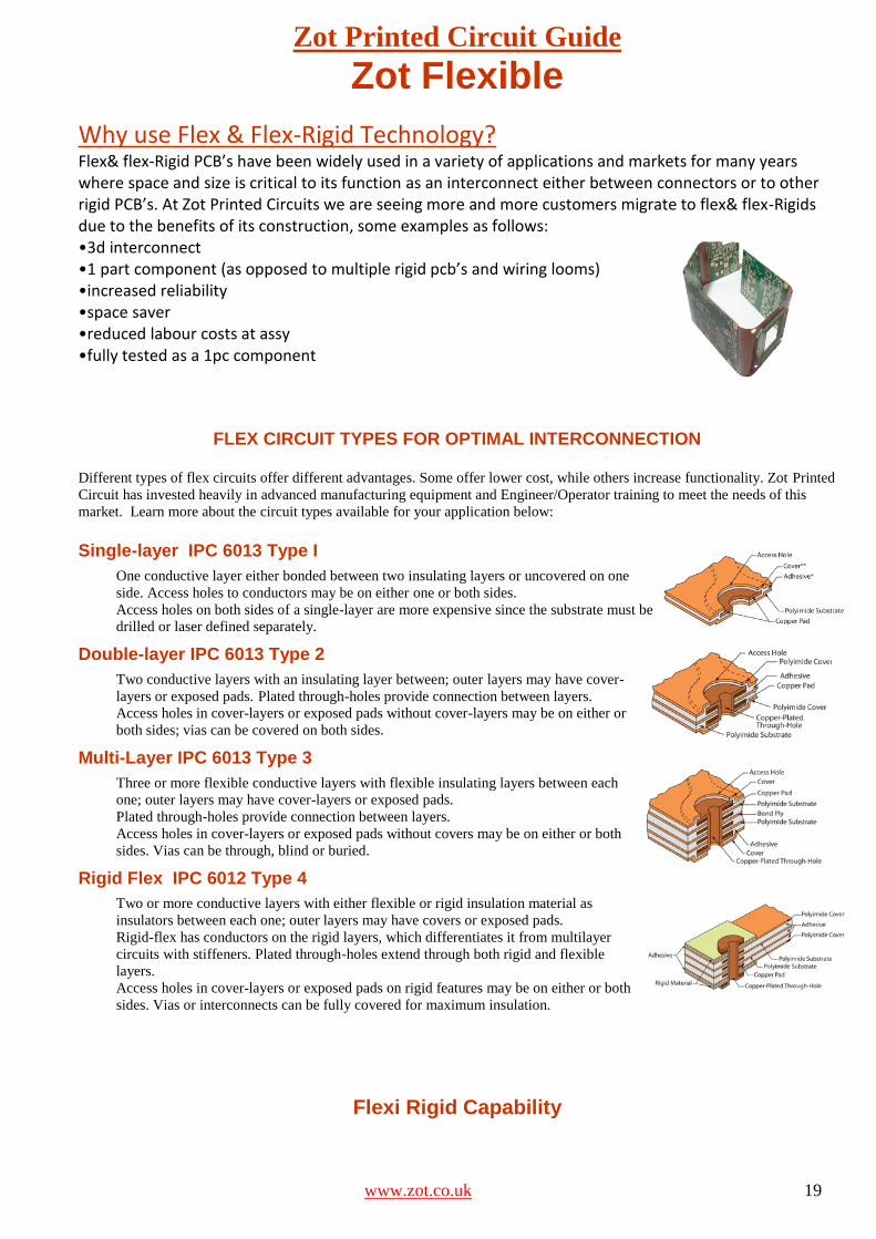
Single-layer IPC 6013 Type I
One conductive layer either bonded between two insulating layers or uncovered on one
side. Access holes to conductors may be on either one or both sides.
Access holes on both sides of a single-layer are more expensive since the substrate must be
drilled or laser defined separately.
Double-layer IPC 6013 Type 2
Two conductive layers with an insulating layer between; outer layers may have cover-
layers or exposed pads. Plated through-holes provide connection between layers.
Access holes in cover-layers or exposed pads without cover-layers may be on either or
both sides; vias can be covered on both sides.
Multi-Layer IPC 6013 Type 3
Three or more flexible conductive layers with flexible insulating layers between each
one; outer layers may have cover-layers or exposed pads.
Plated through-holes provide connection between layers.
Access holes in cover-layers or exposed pads without covers may be on either or both
sides. Vias can be through, blind or buried.
Rigid Flex IPC 6012 Type 4
Two or more conductive layers with either flexible or rigid insulation material as
insulators between each one; outer layers may have covers or exposed pads. Rigid-flex has conductors on the rigid layers, which differentiates it from multilayer
circuits with stiffeners. Plated through-holes extend through both rigid and flexible
layers.
Access holes in cover-layers or exposed pads on rigid features may be on either or both
sides. Vias or interconnects can be fully covered for maximum insulation.
Flexi Rigid Capability
Zot Printed Circuit Guide
www.zot.co.uk 20
The following is our flexi-rigid capability, this is different from our normal capability.
Attribute Standard
Production Development
/Prototype Future
Development
Panel Size 18 x 12 24x18
Minimum Track Width 0.125mm 0.100mm 0.075mm
Maximum no. of Layers 10 16 -----
Maximum Thickness 2.40mm 3.00mm 4.00mm
Track to Flexi Rigid Tail –Note 1 1.00mm 0.45mm -----
Minimum Internal Annular Ring 0.150mm 0.100mm 0.150mm
Minimum External Annular Ring 0.150mm 0.100mm 0.100mm
Minimum Flexible Core Thickness 0.025mm -----
Flex Materials Dupont – AP Dupont – LF Espanex Tori
Notes
1. The minimum that a pad or track can be to the start of the flexible tail is shown above on the
diagram, and in the table. 2. Flex – Rigid can be combined with HDI designs for the ultimate solution. Please contact us for
details at [email protected]. See below for HDI capability.
See Note 1

Zot Printed Circuit Guide
www.zot.co.uk 21
Flexible PCB Benefits
•Flex Properties –Heat dissipation, shock and vibration resistant –Electrical characteristics: predictable and controllable (impedance, cross-talk, noise) –Versatile shape enables 3-dimensional configurations •Weight and Size –Allows dramatic reduction of electronics package size and weight (up to 75% compared to rigid and round wire configurations) •Cost effective –Designed to eliminate board to board interconnects or board to wire connections (the most common failure points in electronic assemblies) –Easier to install or replace (removes human-error associated with point to point wire assemblies) •Durability –Bend & straighten up to 500 million times without a failure–Unmatched performance for applications with repetitive motion –Polyimide is known for its dimensional stability, dielectric strength and high heat resistance
Flex Board Applications
Defence and Aerospace •Replacing many wire harnesses for ruggedized applications, flexible circuit boards are able to survive hostile environments. •Weight reduction paired with increased reliability. •Field serviceability. Medical •Dramatic reduction of overall electronics package size. •Weight reduction enables handheld and portable devices. •Resistance to chemically aggressive environments enables implantable devices. Industrial Controls •With the ability to bend and straighten millions of times without a failure, flex circuits provide un-matched performance for applications with repetitive motion. •Durability and reliability in aggressive environments. Consumer Electronics •Weight reduction is key for hand-held devices, personal computing, GPS, cell phones. •Stability of materials for high volume manufacturing.
The Basics: Materials
Zot Printed Circuit Guide
www.zot.co.uk 22
Copper Clad Laminates •Rolled Annealed (RA) copper •Electro-Deposited (ED) copper •¼ oz (ED) to 3 oz Cu weights Kapton® -DuPont's trademark for polyimide film Pyralux® -DuPont's trademark for flexible circuit materials (Cu clad laminates, coverlays and bonding adhesives) Coverlay –Kapton coated with adhesive on one side (insulating material that is applied over a conductive pattern on the outer surface of the pcb) Bondply –Kapton coated with adhesive on both sides
Flex Materials are certified to IPC-4202, 4203 and 4204 •Adhesiveless copper clad laminate –AP (excellent thermal, chemical, electrical and mechanical properties) ideal for rigid flex and multilayer flex •Acrylic Adhesive Based clad laminates –LF (High Reliability) Avionics –FR (Fire Retardant) Commercial Grade, UL 94 V0 •Stiffeners –FR4 or other material that is bonded to the FCB to provide mechanical support •Rigid Multilayer Materials for Rigid- Flex Constructions: .FR4 .Polyimide .RF Materials, Reinforced PTFE
TYPICAL PROPERTIES OF DIELECTRIC MATERIAL FOR FLEXIBLE PRINTED CIRCUITRY
PROPERTY (TYPICAL) UNITS POLYIMIDE POLYIMIDE
(Adhesiveless)
POLYESTER
REPRESENTATIVE TRADE NAME KAPTON KAPTON MYLAR
PHYSICAL
Thickness Range mil 0.5 to 5 1-6 2-5
Tensile Strength (@25° C) psi 25,000 50,000 20,000 to
35,000
Break Elongation % 70 50 60 to 165
Tensile Modulus (@25° C) 100,000 psi 4.3 .7 5
Tear Initiation Strength lb/in 1000 700-1200 1000 to 1500
Tear Propagation Strength g/mil 8 20 12 to 25
CHEMICAL
Resistance to:
Strong Acids Good Good Good
Strong Alkalis Poor Good Poor
Grease and Oil Good Good Good
Organic Solvents Good Good Good
Water Good Good Good
Sunlight Good Good Fair
Fungus Non-nutrient Non-nutrient Non-nutrient
Water Absorption (ASTM D570) % (24 hours) 2.9 .8 <0.8
THERMAL
Service Temperature (min/max) degree C -125/+200 -125/+200 -60/+105
Coefficient of Thermal Expansion
(@22°C)
PPM/degree C 20 20 27
Change in Linear Dimensions
(100° C, 30 min)
% <0.3 0.04-0.02 <0.5
ELECTRICAL
DIELECTRIC CONSTANT (ASTM D150) 1MHz 3.4 3.4 3
DISSIPATION FACTOR (ASTM D150) 1MHz 0.01 .003 0.018
DIELECTRIC STRENGTH (ASTM D149)
@ 1 mil thickness
Volume Resistivity (ASTM D257)
V/mil
ohm-cm
6000
1.0E+16
6000
1.0E+16
3400
1.0E+1
Zot Printed Circuit Guide
www.zot.co.uk 23
Design Considerations
Minimum Bend Radius •For single and double sided flex the minimum bend radius should be 6 times the overall thickness. •For multilayer and rigid flex, the minimum bend radius should be 12 times the overall thickness. •Critical area is the inside of the bend where delamination, dielectric and conductor fractures can occur. •Failures in the compression area (Inside of the bend) may go undetected until after the FCB is in service. •This is the most common mechanical failure mechanism for a flex board and it can happen with just one excessive fold of the board. •Elevated PCB temperature during bending is not recommended.
Designer Tips:
.Even distribution of copper features in the bend area. .Power & ground planes on the outside of the bend and cross-hatched. .For border-line conditions there is no substitute for a mechanical mock-up that can be destructively tested after bend.
Flex Tear Prevention •Second most common mechanical failure mode for flex and rigid-flex. •Can be caused by mis- handling as well as fatigue from repetitive motion. •Tear Stops: unterminated (or grounded) conductors placed at or near corners to stop tear propagation, may run the entire length of the board. •Rounded Corners: where possible inside radii should be .030” or greater. Eliminate sharp edges wherever possible.
Designer Tips: .Avoid 90 degree corners, applies to inside and outside corners. .Avoid mechanical stress build-up caused by un- even circuitry. Route traces with rounded or 45 degree corners in critical areas. .Allowspace for tear stops in the vicinity of inside corners.
Zot Printed Circuit Guide
www.zot.co.uk 24
Design Considerations
Balanced Circuitry
•Allows mechanical stress to distribute
evenly when circuit is flexed repeatedly perpendicular to the conductors. •Absolutely necessary for any dynamic flex applications (single sided, double sided and multi-layer), highly recommended for all constructions. •Prevents higher stress conditions to develop around isolated traces or other copper features.
Designer Tips:
.Balance geometry of copper vs. void areas as much as possible. .Add un-terminated (or grounded) copper pour to even distribution if necessary. .Adjust width of flex area to avoid large void areas if possible.
Maximize Conductor Widths •Tear Drops (Pad Fillets): improve mechanical and electrical reliability for both innerlayer and outerlayer connections. •Improved reliability when drills are not perfectly centred on pads. •Tear drops can be added globally in CAM (requires customer approval). •“Anchoring Spurs” to be used on outerlayer pads only to help prevent lifted pads during soldering operations. •Improve manufacturability, increase yield, lower PCB costs.
Designer Tips: .Use wider traces where possible, also helps balancing copper/void areas. .Add or require tear drops to all inner and outer layer pads (including SMT pads). .Add anchoring spurs or square copper pads with round coverlay opening when possible.
Zot Printed Circuit Guide
www.zot.co.uk 25
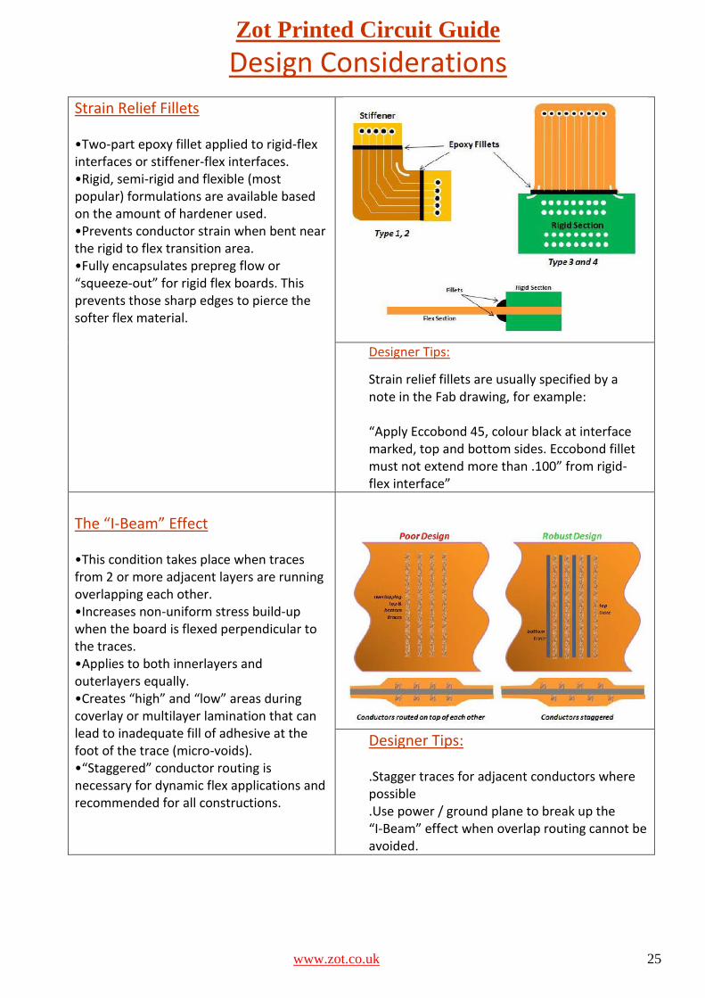
Design Considerations
Strain Relief Fillets •Two-part epoxy fillet applied to rigid-flex interfaces or stiffener-flex interfaces. •Rigid, semi-rigid and flexible (most popular) formulations are available based on the amount of hardener used. •Prevents conductor strain when bent near the rigid to flex transition area. •Fully encapsulates prepreg flow or “squeeze-out” for rigid flex boards. This prevents those sharp edges to pierce the softer flex material.
Designer Tips:
Strain relief fillets are usually specified by a note in the Fab drawing, for example: “Apply Eccobond 45, colour black at interface marked, top and bottom sides. Eccobond fillet must not extend more than .100” from rigid- flex interface”
The “I-Beam” Effect •This condition takes place when traces from 2 or more adjacent layers are running overlapping each other. •Increases non-uniform stress build-up when the board is flexed perpendicular to the traces. •Applies to both innerlayers and outerlayers equally. •Creates “high” and “low” areas during coverlay or multilayer lamination that can lead to inadequate fill of adhesive at the foot of the trace (micro-voids). •“Staggered” conductor routing is necessary for dynamic flex applications and recommended for all constructions.
Designer Tips: .Stagger traces for adjacent conductors where possible .Use power / ground plane to break up the “I-Beam” effect when overlap routing cannot be avoided.
Zot Printed Circuit Guide
www.zot.co.uk 26
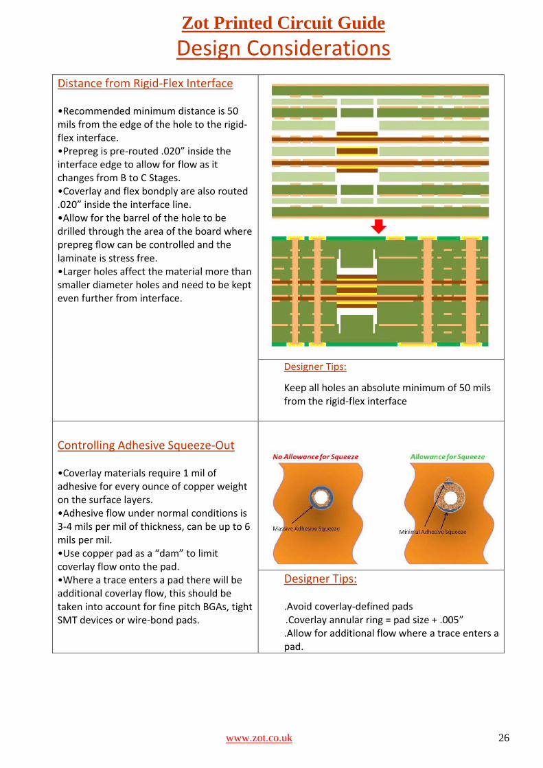
Design Considerations
Distance from Rigid-Flex Interface •Recommended minimum distance is 50 mils from the edge of the hole to the rigid-flex interface. •Prepreg is pre-routed .020” inside the interface edge to allow for flow as it changes from B to C Stages. •Coverlay and flex bondply are also routed .020” inside the interface line. •Allow for the barrel of the hole to be drilled through the area of the board where prepreg flow can be controlled and the laminate is stress free. •Larger holes affect the material more than smaller diameter holes and need to be kept even further from interface.
Designer Tips:
Keep all holes an absolute minimum of 50 mils from the rigid-flex interface
Controlling Adhesive Squeeze-Out •Coverlay materials require 1 mil of adhesive for every ounce of copper weight on the surface layers. •Adhesive flow under normal conditions is 3-4 mils per mil of thickness, can be up to 6 mils per mil. •Use copper pad as a “dam” to limit coverlay flow onto the pad. •Where a trace enters a pad there will be additional coverlay flow, this should be taken into account for fine pitch BGAs, tight SMT devices or wire-bond pads.
Designer Tips: .Avoid coverlay-defined pads
.Coverlay annular ring = pad size + .005” .Allow for additional flow where a trace enters a pad.
Zot Printed Circuit Guide
www.zot.co.uk 27
Design Considerations
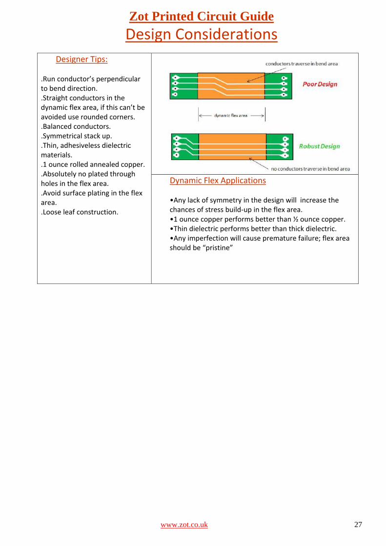
Designer Tips:
.Run conductor’s perpendicular to bend direction. .Straight conductors in the dynamic flex area, if this can’t be avoided use rounded corners. .Balanced conductors. .Symmetrical stack up. .Thin, adhesiveless dielectric materials. .1 ounce rolled annealed copper. .Absolutely no plated through holes in the flex area. .Avoid surface plating in the flex area. .Loose leaf construction.
Dynamic Flex Applications •Any lack of symmetry in the design will increase the chances of stress build-up in the flex area. •1 ounce copper performs better than ½ ounce copper. •Thin dielectric performs better than thick dielectric. •Any imperfection will cause premature failure; flex area should be “pristine”
Zot Printed Circuit Guide
www.zot.co.uk 28
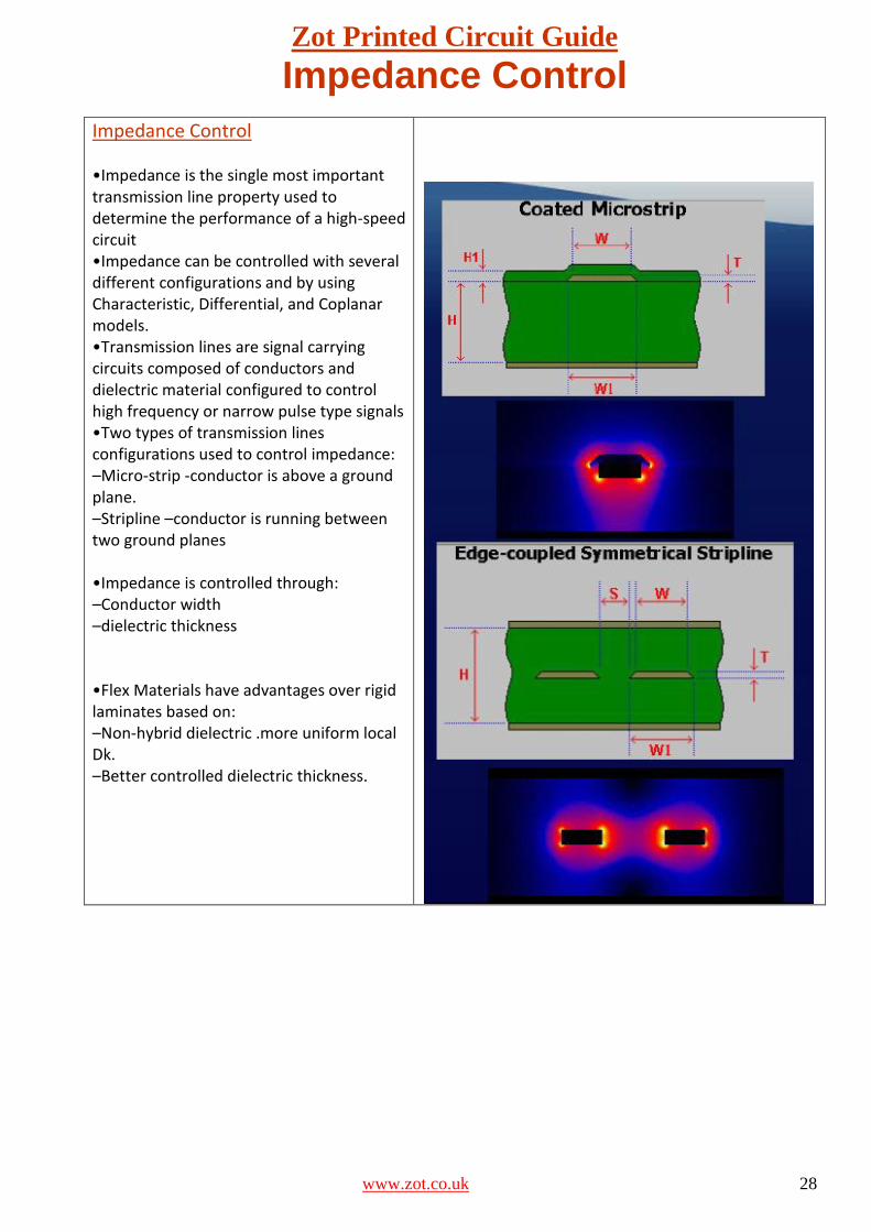
Impedance Control
Impedance Control •Impedance is the single most important transmission line property used to determine the performance of a high-speed circuit •Impedance can be controlled with several different configurations and by using Characteristic, Differential, and Coplanar models. •Transmission lines are signal carrying circuits composed of conductors and dielectric material configured to control high frequency or narrow pulse type signals •Two types of transmission lines configurations used to control impedance: –Micro-strip -conductor is above a ground plane. –Stripline –conductor is running between two ground planes •Impedance is controlled through: –Conductor width –dielectric thickness •Flex Materials have advantages over rigid laminates based on: –Non-hybrid dielectric .more uniform local Dk. –Better controlled dielectric thickness.
Zot Printed Circuit Guide
www.zot.co.uk 29
Controlled Impedance
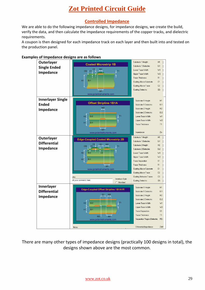
We are able to do the following impedance designs, for impedance designs, we create the build, verify the data, and then calculate the impedance requirements of the copper tracks, and dielectric requirements. A coupon is then designed for each impedance track on each layer and then built into and tested on the production panel. Examples of Impedance designs are as follows
Outerlayer Single Ended Impedance
Innerlayer Single Ended Impedance
Outerlayer Differential Impedance
Innerlayer Differential Impedance
There are many other types of impedance designs (practically 100 designs in total), the designs shown above are the most common.
Zot Printed Circuit Guide
www.zot.co.uk 30
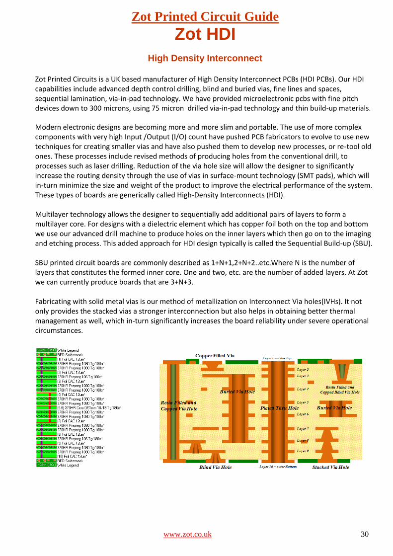
Zot HDI
High Density Interconnect
Zot Printed Circuits is a UK based manufacturer of High Density Interconnect PCBs (HDI PCBs). Our HDI capabilities include advanced depth control drilling, blind and buried vias, fine lines and spaces, sequential lamination, via-in-pad technology. We have provided microelectronic pcbs with fine pitch devices down to 300 microns, using 75 micron drilled via-in-pad technology and thin build-up materials.
Modern electronic designs are becoming more and more slim and portable. The use of more complex components with very high Input /Output (I/O) count have pushed PCB fabricators to evolve to use new techniques for creating smaller vias and have also pushed them to develop new processes, or re-tool old ones. These processes include revised methods of producing holes from the conventional drill, to processes such as laser drilling. Reduction of the via hole size will allow the designer to significantly increase the routing density through the use of vias in surface-mount technology (SMT pads), which will in-turn minimize the size and weight of the product to improve the electrical performance of the system. These types of boards are generically called High-Density Interconnects (HDI). Multilayer technology allows the designer to sequentially add additional pairs of layers to form a multilayer core. For designs with a dielectric element which has copper foil both on the top and bottom we use our advanced drill machine to produce holes on the inner layers which then go on to the imaging and etching process. This added approach for HDI design typically is called the Sequential Build-up (SBU). SBU printed circuit boards are commonly described as 1+N+1,2+N+2..etc.Where N is the number of layers that constitutes the formed inner core. One and two, etc. are the number of added layers. At Zot we can currently produce boards that are 3+N+3. Fabricating with solid metal vias is our method of metallization on Interconnect Via holes(IVHs). It not only provides the stacked vias a stronger interconnection but also helps in obtaining better thermal management as well, which in-turn significantly increases the board reliability under severe operational circumstances.
Zot Printed Circuit Guide
www.zot.co.uk 31
HDI Capability
HDI general description
Printed circuit board with a higher wiring density per unit area than conventional printed circuit boards (PCB). They have finer lines and spaces (≤ 100 μm), smaller vias (<150 μm) and capture pads (<400 μm), and higher connection pad density (>20 pads/cm2) than employed in conventional PCB technology.
IPC-2226 definition of Microvia: A blind hole with a diameter of less than or equal to 150 μm having a pad diameter of less than or equal to 350μm formed by either laser or mechanically drilling.
IPC-T-50H: High Density Interconnect (HDI) A generic term for substrates or boards with a higher circuit density per unit area than conventional printed boards
At Zot we use mechanical drilling down to 0.120mm diameter, for smaller microvia laser drilling is used.
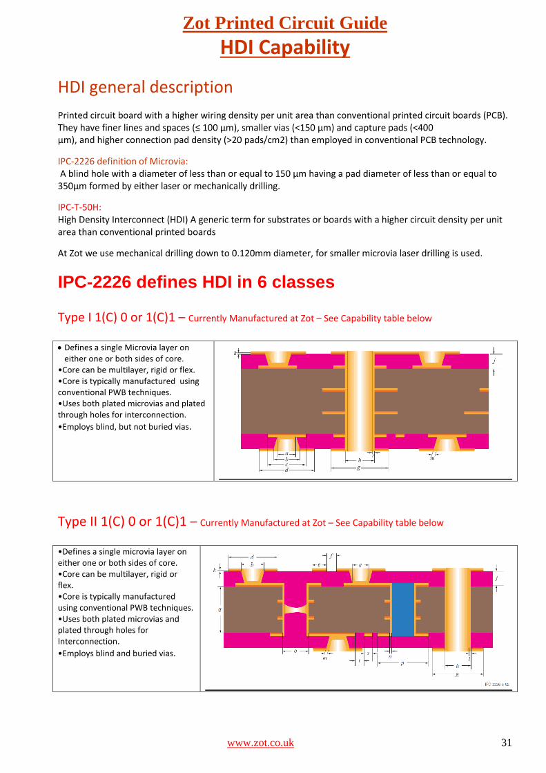
IPC-2226 defines HDI in 6 classes Type I 1(C) 0 or 1(C)1 – Currently Manufactured at Zot – See Capability table below
Defines a single Microvia layer on
either one or both sides of core. •Core can be multilayer, rigid or flex. •Core is typically manufactured using conventional PWB techniques. •Uses both plated microvias and plated through holes for interconnection.
•Employs blind, but not buried vias.
Type II 1(C) 0 or 1(C)1 – Currently Manufactured at Zot – See Capability table below
•Defines a single microvia layer on either one or both sides of core. •Core can be multilayer, rigid or flex. •Core is typically manufactured using conventional PWB techniques. •Uses both plated microvias and plated through holes for Interconnection.
•Employs blind and buried vias.
Zot Printed Circuit Guide
www.zot.co.uk 32
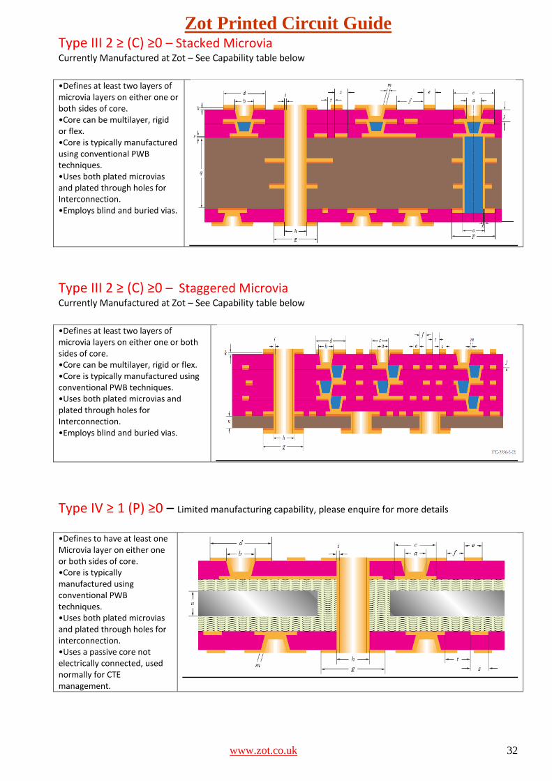
Type III 2 ≥ (C) ≥0 – Stacked Microvia Currently Manufactured at Zot – See Capability table below
•Defines at least two layers of microvia layers on either one or both sides of core. •Core can be multilayer, rigid or flex. •Core is typically manufactured using conventional PWB techniques. •Uses both plated microvias and plated through holes for Interconnection. •Employs blind and buried vias.
Type III 2 ≥ (C) ≥0 – Staggered Microvia Currently Manufactured at Zot – See Capability table below
•Defines at least two layers of microvia layers on either one or both sides of core. •Core can be multilayer, rigid or flex. •Core is typically manufactured using conventional PWB techniques. •Uses both plated microvias and plated through holes for Interconnection. •Employs blind and buried vias.
Type IV ≥ 1 (P) ≥0 – Limited manufacturing capability, please enquire for more details
•Defines to have at least one Microvia layer on either one or both sides of core. •Core is typically manufactured using conventional PWB techniques. •Uses both plated microvias and plated through holes for interconnection. •Uses a passive core not electrically connected, used normally for CTE management.
Zot Printed Circuit Guide
www.zot.co.uk 33
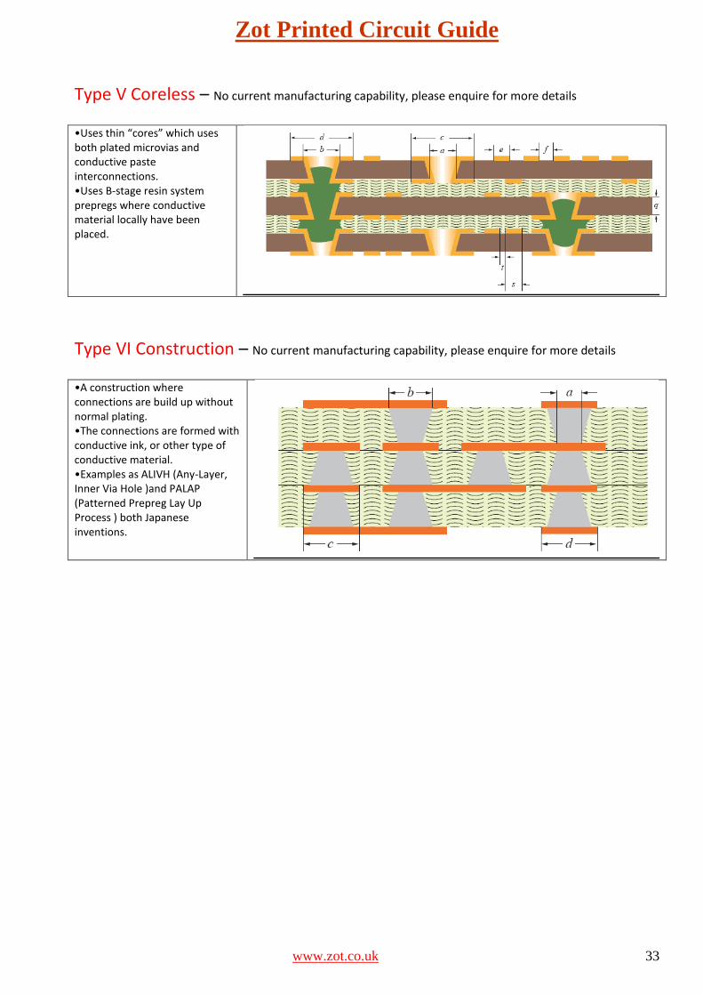
Type V Coreless – No current manufacturing capability, please enquire for more details
•Uses thin “cores” which uses both plated microvias and conductive paste interconnections. •Uses B-stage resin system prepregs where conductive material locally have been placed.
Type VI Construction – No current manufacturing capability, please enquire for more details
•A construction where connections are build up without normal plating. •The connections are formed with conductive ink, or other type of conductive material. •Examples as ALIVH (Any-Layer, Inner Via Hole )and PALAP (Patterned Prepreg Lay Up Process ) both Japanese inventions.
Zot Printed Circuit Guide
www.zot.co.uk 34
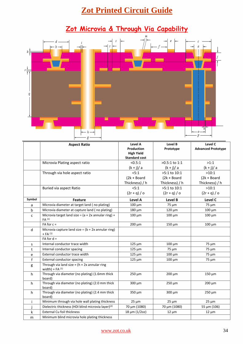
Zot Microvia & Through Via Capability
Aspect Ratio Level A Production High Yield
Standard cost
Level B Prototype
Level C Advanced Prototype
Microvia Plating aspect ratio <0.5:1 (k + j)/ a
>0.5:1 to 1:1 (k + j)/ a
>1:1 (k + j)/ a
Through via hole aspect ratio <5:1 (2k + Board
Thickness) / h
>5:1 to 10:1 (2k + Board
Thickness) / h
>10:1 (2k + Board
Thickness) / h
Buried via aspect Ratio <5:1 (2r + q) / o
>5:1 to 10:1 (2r + q) / o
>10:1 (2r + q) / o
Symbol Feature Level A Level B Level C a Microvia diameter at target land ( no plating) 100 μm 75 μm 75 μm
b Microvia diameter at capture land ( no plating) 180 μm 120 μm 100 μm
c Microvia target land size = (a + 2x annular ring) + FA (1)
100 μm 100 μm 100 μm
FA for c = 200 μm 150 μm 100 μm
d Microvia capture land size = (b + 2x annular ring) + FA (1)
FA for d =
s Internal conductor trace width 125 μm 100 μm 75 μm
t Internal conductor spacing 125 μm 75 μm 75 μm
e External conductor trace width 125 μm 100 μm 75 μm
f External conductor spacing 125 μm 100 μm 75 μm
g Through via land size = (h + 2x annular ring width) + FA (1)
h Through via diameter (no plating) (1.6mm thick board)
250 μm 200 μm 150 μm
h Through via diameter (no plating) (2.0 mm thick board)
300 μm 250 μm 200 μm
h Through via diameter (no plating) (2.4 mm thick board)
350 μm 300 μm 250 μm
i Minimum through via hole wall plating thickness 25 μm 25 μm 25 μm
j Dielectric thickness (HDI blind microvia layer)(2) 70 μm (1080) 70 μm (1080) 55 μm (106)
k External Cu foil thickness 18 μm (1/2oz) 12 μm 12 μm
m Minimum blind microvia hole plating thickness
Zot Printed Circuit Guide
www.zot.co.uk 35
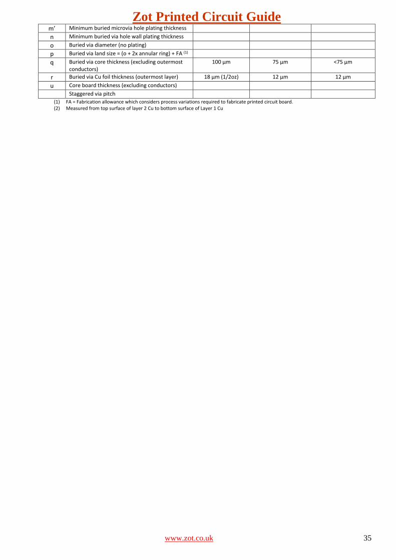
m’ Minimum buried microvia hole plating thickness
n Minimum buried via hole wall plating thickness
o Buried via diameter (no plating)
p Buried via land size = (o + 2x annular ring) + FA (1)
q Buried via core thickness (excluding outermost conductors)
100 μm 75 μm <75 μm
r Buried via Cu foil thickness (outermost layer) 18 μm (1/2oz) 12 μm 12 μm
u Core board thickness (excluding conductors)
Staggered via pitch
(1) FA = Fabrication allowance which considers process variations required to fabricate printed circuit board. (2) Measured from top surface of layer 2 Cu to bottom surface of Layer 1 Cu
Zot Printed Circuit Guide
www.zot.co.uk 36
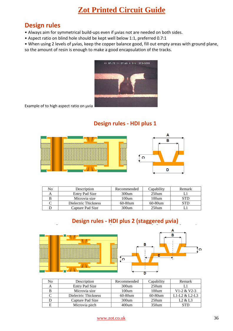
Design rules • Always aim for symmetrical build-ups even if μvias not are needed on both sides. • Aspect ratio on blind hole should be kept well below 1:1, preferred 0.7:1 • When using 2 levels of μvias, keep the copper balance good, fill out empty areas with ground plane, so the amount of resin is enough to make a good encapsulation of the tracks.
Example of to high aspect ratio on μvia
Design rules - HDI plus 1
No Description Recommended Capability Remark
A Entry Pad Size 300um 250um L1
B Microvia size 100um 100um STD
C Dielectric Thickness 60-80um 60-80um STD
D Capture Pad Size 300um 250um L1
Design rules - HDI plus 2 (staggered µvia)
No Description Recommended Capability Remark
A Entry Pad Size 300um 250um L1
B Microvia size 100um 100um V1-2 & V2-3
C Dielectric Thickness 60-80um 60-80um L1-L2 & L2-L3
D Capture Pad Size 300um 250um L2 & L3
E Microvia pitch 400um 350um STD
Zot Printed Circuit Guide
www.zot.co.uk 37
Design rules - HDI plus 2 (stepped µvia)
No Description Recommended Capability Remark
A Microvia size 200um 200um V1-2
B Microvia size 100um 100um V2-3
C Dielectric Thickness 60-80um 60-80um L1-L2 & L2-L3
D Capture Pad Size 300um 250um L3
E Entry/Capture Pad Size 400um 350um L2
F Entry/Pad Size 400um 350um L1
Design rules - HDI plus 2 (stepped µvia)
No Description Recommended Capability Remark
A Microvia size 200um 200um V1-3
B Entry pad size 100um 100um L1
C Dielectric Thickness 60-80um 60-80um L1-L3 max
D Capture Pad Size 300um 250um L3
E Anti-Pad Size 400um 350um L2 min
Design rules - HDI plus 2 (stacked µvia)
No Description Recommended Capability Remark
A Entry pad size 300um 250um L1
B Microvia size 200um 200um V1-2 & V2-3
C Dielectric Thickness 60-80um 60-80um L1-L2 & L2-L3
D Capture Pad Size 400um 350um L2&L3
Zot Printed Circuit Guide
www.zot.co.uk 38
µvia between L2- L3 need to be copper filled µvia between L2- L1 optional to be copper filled
Design rules - HDI plus 2 (µvia on buried pad)
No Description Recommended Capability Remark
A Entry pad size 300um 250um L1
B Microvia size 200um 200um V1-2
C Dielectric Thickness 60-80um 60-80um L1-L2
D Capture Pad Size 400um 350um L2
E Buried Hole size* 300um 200um
*Core thickness dependant, see above for aspect ratio
Note: a. Always keep dielectric spacing for blind vias as low as possible ; 1 x 10⁶ prepreg (54 micron) or 1 x 1080 prepreg (70 micron) are the best for manufacturing, to increase reliability and reduce cost. b. Maximum Sequential Pressing = 4 pressing Cycles. c. Blind microvia can be copper filled or resin filled and copper plated over, please ask for
details.
Zot Printed Circuit Guide
www.zot.co.uk 39
Via in PAD Technology – Copper Filled Microvia With the ever increasing miniaturisation of components, and the need to put more in a smaller space, we have commissioned a process, which can fill microvias with copper to plate them shut.
This technology is typically used in BGAs to put the via in the pad enabling greater routing of signal tracking, and removing the problem of voids in the solder joint caused by air entrapment during the printing of solder paste, that could be trapped in the non-filled via. What Via configuration can we copper fil. In order to plate vias shut, the via needs to be no more than a certain depth drilled and no more than a certain diameter, in order not to overplate the outerlayer circuitry. It is possible to plate shut other depth/diameters, however we would then need additional planarization processes to reduce outerlayer copper weight for etching the final circuit pattern.
Die
lec
tric (m
icro
n)
Cre
ate
d b
y
Ou
ter C
op
pe
r
Drill S
ize
Ho
le D
iam
ete
r - To
p
of T
ap
ere
d H
ole
s
Drill D
ep
th
Co
pp
er V
ia
Fill
55 1*106 12 120 105 85 Default
70 1*1080 12 150 116 100 YES
100 2*106 12 200 170 140 Possible Reduced yield Increase cost
132 2*1080 12 250 185 170 Possible Reduced yield Increase cost
Larger dielectrics are possible to copper fill, please ask for advice
Definition of a Plated Shut Via. We define a plated shut via, as having a dimple less than 10 microns.
Using Vias in pads on BGAs without
plating them shut can lead to voids
in the solder joints
Zot Printed Circuit Guide
www.zot.co.uk 40
Zot IPC 4761 Via Plugging Guide
IPC-4761 - Summary of Specification IPC-4761 reflects IPC's work towards standardizing the via plugging process. To summarize, this document classifies 7 different types of via plugs. Two of these are dedicated to the use of dry film soldermask, which now has only limited usage and applications. From what we know, this usage is primarily limited to older military applications. The remainder, we would separate between via plugging and Via-in-Pad as these two types of via plugs serve very different purposes. Historically, and even continuing to today, the requirement for via plugging in designs has simply been called out as "via must be plugged", with some diligent designers calling out that they must be plugged with an epoxy. Overall, this is a very ambiguous callout that IPC-4761 serves to lend discipline and clarity to. Here's a summary of the different types of via plugs called out in this document:
Photographic Examples of Various Types of Via Plugging
Since we are a provider of commercial printed circuit boards, we most often encounter the middle grouping of via plug types (III, IV, V, & VI), which we be the focus of this article. Reviewing the IPC 4761 document from Type III through Type VI, I can't help but think that this is somewhat of a dangerous document. Based on my experience in plugging vias, I would say that types III and IV are nothing but an incremental step on the way to achieving a Type V or VI via. Now, it's very easy to look at a cartoon picture and say "That's what I want!" and include that in your fabrication notes. It's whole other story when you actually have to achieve in real life what the nice cartoon depicts. With larger via sizes (0.016" and up) in a 0.062" typical thickness PCB, achieving a Type V or VI via plug is not too difficult--though still time consuming. However, trying to screen a low shrinkage ink into a 0.012" via (and often down to 0.008") and fill it entirely is a much more difficult target to hit. Given the difficulties in achieving a Type VI(b) via fill, IPC should almost create a Type VI(c), which depicts the attempt at a Type VI in which the plugging ink only fills a portion of the via, and the rest of it is filled with soldermask. While this may not be technically correct, I would wager that this is what most actual boards look like given the difficulty in achieving a full plug.
Zot Printed Circuit Guide
www.zot.co.uk 41
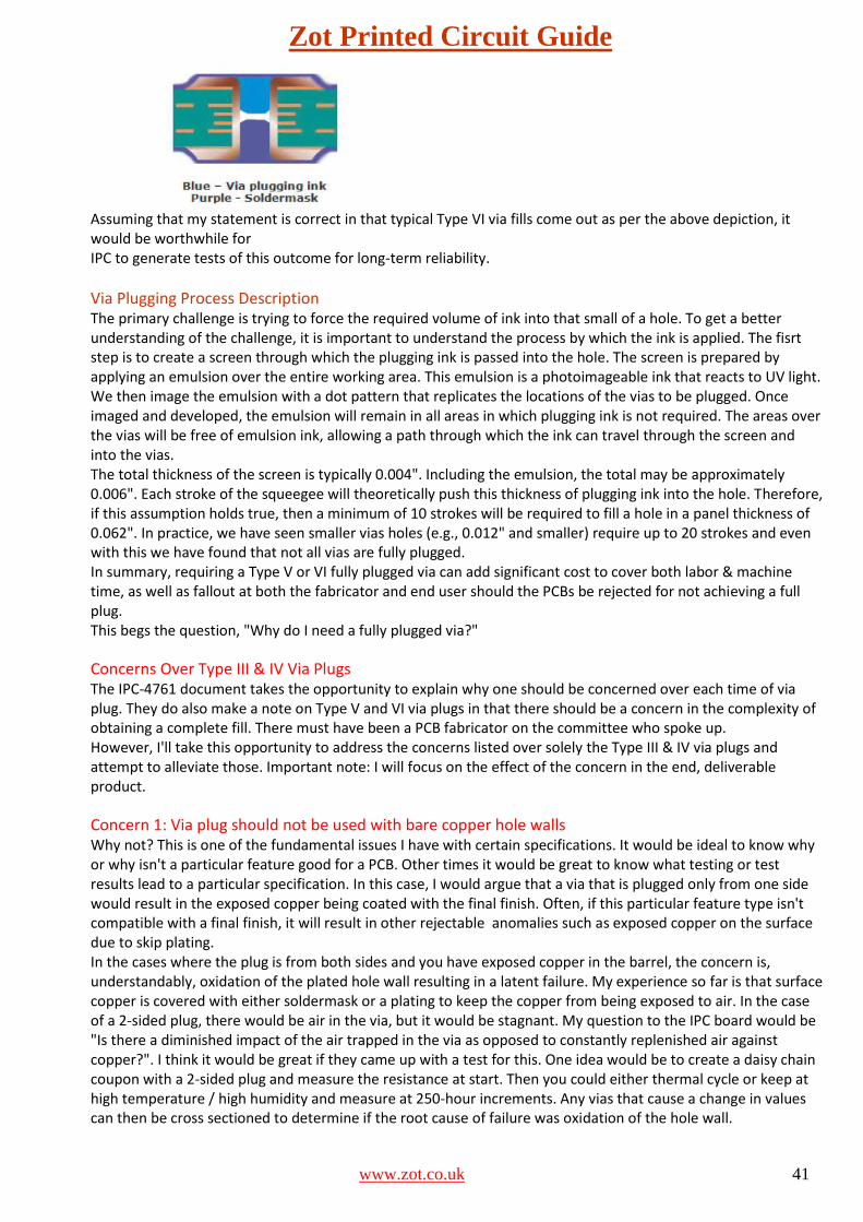
Assuming that my statement is correct in that typical Type VI via fills come out as per the above depiction, it would be worthwhile for IPC to generate tests of this outcome for long-term reliability.
Via Plugging Process Description The primary challenge is trying to force the required volume of ink into that small of a hole. To get a better understanding of the challenge, it is important to understand the process by which the ink is applied. The fisrt step is to create a screen through which the plugging ink is passed into the hole. The screen is prepared by applying an emulsion over the entire working area. This emulsion is a photoimageable ink that reacts to UV light. We then image the emulsion with a dot pattern that replicates the locations of the vias to be plugged. Once imaged and developed, the emulsion will remain in all areas in which plugging ink is not required. The areas over the vias will be free of emulsion ink, allowing a path through which the ink can travel through the screen and into the vias. The total thickness of the screen is typically 0.004". Including the emulsion, the total may be approximately 0.006". Each stroke of the squeegee will theoretically push this thickness of plugging ink into the hole. Therefore, if this assumption holds true, then a minimum of 10 strokes will be required to fill a hole in a panel thickness of 0.062". In practice, we have seen smaller vias holes (e.g., 0.012" and smaller) require up to 20 strokes and even with this we have found that not all vias are fully plugged. In summary, requiring a Type V or VI fully plugged via can add significant cost to cover both labor & machine time, as well as fallout at both the fabricator and end user should the PCBs be rejected for not achieving a full plug. This begs the question, "Why do I need a fully plugged via?"
Concerns Over Type III & IV Via Plugs The IPC-4761 document takes the opportunity to explain why one should be concerned over each time of via plug. They do also make a note on Type V and VI via plugs in that there should be a concern in the complexity of obtaining a complete fill. There must have been a PCB fabricator on the committee who spoke up. However, I'll take this opportunity to address the concerns listed over solely the Type III & IV via plugs and attempt to alleviate those. Important note: I will focus on the effect of the concern in the end, deliverable product.
Concern 1: Via plug should not be used with bare copper hole walls Why not? This is one of the fundamental issues I have with certain specifications. It would be ideal to know why or why isn't a particular feature good for a PCB. Other times it would be great to know what testing or test results lead to a particular specification. In this case, I would argue that a via that is plugged only from one side would result in the exposed copper being coated with the final finish. Often, if this particular feature type isn't compatible with a final finish, it will result in other rejectable anomalies such as exposed copper on the surface due to skip plating. In the cases where the plug is from both sides and you have exposed copper in the barrel, the concern is, understandably, oxidation of the plated hole wall resulting in a latent failure. My experience so far is that surface copper is covered with either soldermask or a plating to keep the copper from being exposed to air. In the case of a 2-sided plug, there would be air in the via, but it would be stagnant. My question to the IPC board would be "Is there a diminished impact of the air trapped in the via as opposed to constantly replenished air against copper?". I think it would be great if they came up with a test for this. One idea would be to create a daisy chain coupon with a 2-sided plug and measure the resistance at start. Then you could either thermal cycle or keep at high temperature / high humidity and measure at 250-hour increments. Any vias that cause a change in values can then be cross sectioned to determine if the root cause of failure was oxidation of the hole wall.
Zot Printed Circuit Guide
www.zot.co.uk 42
Concern 2: Outgassing / Blow-Outs Agreed. But this is a failure mode that the bare board would be rejected for. If the PCB has a HASL finish, then any outgassing concerns would be evident on the bare board as the thermal shock in this process is much greater than that incurred during PCB assembly. If it survives this process, then it should be considered rugged enough to last for the rest of the product's life cycle. Furthermore, if there is a conformal coating / potting process during final assembly, then concerns of exposed copper potentially do not apply. However, this may still be a concern for non-HASL finishes. In any event, this should be pointed out in the IPC document and not for the user to discern.
Concern 3: Removal of chemistries The concern here is that the higher the aspect ratio, the more concern there should be of the removal of chemistries. Agreed. However, this is a bare board concern. Dragging chemistries from one bath to another in most immersion processes results in "skip plating", which manifests itself in exposed surface copper. This is a rejectable PCB characteristic and would never make to the finished product anyway. In the case of a HASL finish, the only chemistries the board should see after the plugging process should be RO Water, which is typically dried out in final washing. Again, it would be great to know exactly which chemistries are of concern so that PCB fabricators can work together with their customers to alleviate.
Summary In summary, while I think this standard did a great job of explaining the differences between the types of available via plugging, I think it needs more work to really define to the end user when each type of plug should be allowable or not. Also, there should be cross qualifications (e.g., a type VI backward qualifies as meeting Type III or IV, etc.). If there's anyone out there willing to put together the testing methodology, I'm more than happy to build the test vehicles.
Zot Printed Circuit Guide
www.zot.co.uk 43
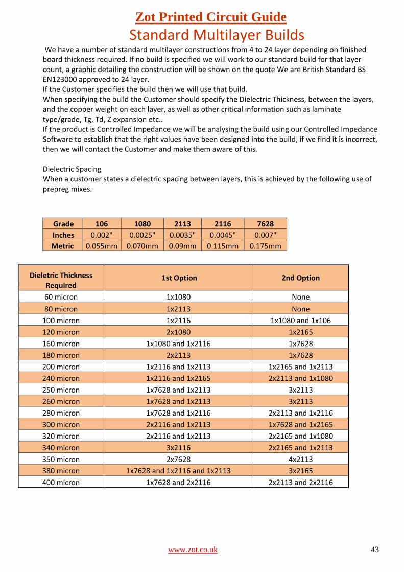
Standard Multilayer Builds We have a number of standard multilayer constructions from 4 to 24 layer depending on finished board thickness required. If no build is specified we will work to our standard build for that layer count, a graphic detailing the construction will be shown on the quote We are British Standard BS EN123000 approved to 24 layer. If the Customer specifies the build then we will use that build. When specifying the build the Customer should specify the Dielectric Thickness, between the layers, and the copper weight on each layer, as well as other critical information such as laminate type/grade, Tg, Td, Z expansion etc.. If the product is Controlled Impedance we will be analysing the build using our Controlled Impedance Software to establish that the right values have been designed into the build, if we find it is incorrect, then we will contact the Customer and make them aware of this. Dielectric Spacing When a customer states a dielectric spacing between layers, this is achieved by the following use of prepreg mixes.
Grade 106 1080 2113 2116 7628
Inches 0.002" 0.0025" 0.0035" 0.0045" 0.007"
Metric 0.055mm 0.070mm 0.09mm 0.115mm 0.175mm
Dieletric Thickness Required
1st Option 2nd Option
60 micron 1x1080 None
80 micron 1x2113 None
100 micron 1x2116 1x1080 and 1x10⁶
120 micron 2x1080 1x2165
160 micron 1x1080 and 1x2116 1x7628
180 micron 2x2113 1x7628
200 micron 1x2116 and 1x2113 1x2165 and 1x2113
240 micron 1x2116 and 1x2165 2x2113 and 1x1080
250 micron 1x7628 and 1x2113 3x2113
260 micron 1x7628 and 1x2113 3x2113
280 micron 1x7628 and 1x2116 2x2113 and 1x2116
300 micron 2x2116 and 1x2113 1x7628 and 1x2165
320 micron 2x2116 and 1x2113 2x2165 and 1x1080
340 micron 3x2116 2x2165 and 1x2113
350 micron 2x7628 4x2113
380 micron 1x7628 and 1x2116 and 1x2113 3x2165
400 micron 1x7628 and 2x2116 2x2113 and 2x2116
Zot Printed Circuit Guide
www.zot.co.uk 44
Default Multilayer Build Constructions Where a multilayer build is not specified, we default to the most cost effective construction. ( combination of prepregs and cores ) Our Standard defaults builds are 1.60mm thick, with 35um internal copper and 35 um finished external copper. Cost effective construction can only be used where there is sufficient prepreg available to encapsulate the innerlayer tracking.
Importance of Prepreg Selection
The function of the prepreg is to provide an insulation layer and fully encapsulate the innerlayer copper. Insulation (Dielectric Breakdown)
The actual dielectric breakdown is typically 1,000 volts per 1 thou ( 25 microns ) of Prepreg This means that was use a minimum of 100 um of prepreg, breakdown is 4,000 volts plus. With some constructions using a lot more, values are typically 40 volts per Micron of prepreg. Encapsulation of Innerlayer Tracking
Prepreg prior to pressing is basically a glass cloth impregnated with a B stage epoxy resin which is then heated to a liquid state under pressure, this then encapsulates the innerlayer tracking, however it must be remembered that all prepreg styles have different thicknesses and resin percentages, and circuit patterns have different amounts of areas to be encapsulated with the resin. The actual resin when liquid does not move very far, so "AVAILABLE RESIN " is a major issue to good encapsulation of innerlayer patterns. Typical Prepreg Resin % are as follows
Style Pressed
Thickness Resin
% Cost
106 0.050mm 75.00% +76%
1080 0.066mm 61.00% Base
2113 0.090mm 56.00% +14%
2116 0.115mm 53.00% Base
7628 0.175mm 42.00% +12%
7628HR 0.200mm 48.00% +20%
As you can see 106 are the thinnest and most expensive, typically this should only be used when you are trying to create a high layer count in a thin construction or when “available resin” is a major issue. As you can also see 2116 is just under twice the thickness of 1080, but they are the same price, and the “available resin “ is similar. Although 7628 or 7628HR ( HR = high resin content ) is by far the most cost effective prepreg, it has the lowest available resin.
Separation Ly1 – Ly2
Separation Ly3 – Ly4
Separation Ly5 – Ly6
Separation Ly7 – Ly8
Separation Ly9 – Ly10
Separation Ly11 – Ly12
4 Layer No Issue
No Issue
6 Layer < 25% Copper Area
<126% combined
Copper Area
< 25% Copper Area
8 Layer < 25% Copper Area
<126% combined
Copper Area
<126% combined
Copper Area
< 25% Copper Area
10 Layer No Issue
<44% combined
Copper Area
<44% combined
Copper Area
<44% combined
Copper Area
No Issue
12 Layer No Issue
<44% combined
Copper Area
<44% combined
Copper Area
<44% combined
Copper Area
<44% combined
Copper Area
No Issue
Zot Printed Circuit Guide
www.zot.co.uk 45
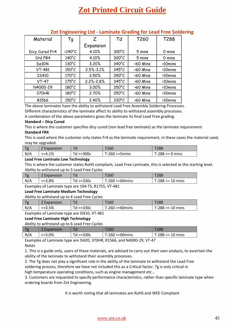
Zot Engineering Ltd - Laminate Grading for Lead Free Soldering
Material Tg Z
Expansion
Td T260 T288
Dicy Cured Fr4 <140°C 4.10% 300°C 5 mins 0 mins
Std FR4 140°C 4.10% 300°C 5 mins 0 mins
De104i 130°C 3.20% 340°C >60 Mins >10mins
VT-481 150°C 2.5%-3.1% 345°C >60 Mins >10mins
IS410 170°C 3.50% 350°C >60 Mins >10mins
VT-47 175°C 2.2%-2.8% 345°C >60 Mins >10mins
N4000-29 180°C 3.00% 350°C >60 Mins >10mins
370HR 180°C 2.70% 350°C >60 Mins >10mins
R1566 150°C 2.40% 330°C >60 Mins >10mins
The above laminates have the ability to withstand Lead Free Assembly Soldering Processes. Different characteristics of the laminate affect its ability to withstand assembly processes. A combination of the above parameters gives the laminate its final Lead Free grading. Standard – Dicy Cured This is where the customer specifies dicy cured (non lead free laminate) as the laminate requirement Standard FR4 This is used where the customer only states Fr4 as the laminate requirement, in these cases the material used, may be upgraded.
Tg Z Expansion Td T260 T288
N/A <=4.1% Td >=300c T-260 >=5mins T-288 >= 0 mins
Lead Free Laminate Low Technology This is where the customer states RoHS compliant, Lead Free Laminate, this is selected as the starting level. Ability to withstand up to 3 Lead Free Cycles
Tg Z Expansion Td T260 T288
N/A <=3.8% Td >=330c T-260 >=60mins T-288 >= 10 mins
Examples of Laminate type are 104-TS, R1755, VT-481 Lead Free Laminate Medium Technology Ability to withstand up to 4 Lead Free Cycles
Tg Z Expansion Td T260 T288
N/A <=3.5% Td >=330c T-260 >=60mins T-288 >= 10 mins
Examples of Laminate type are IS410, VT-481 Lead Free Laminate High Technology Ability to withstand up to 6 Lead Free Cycles
Tg Z Expansion Td T260 T288
N/A <=3.0% Td >=330c T-260 >=60mins T-288 >= 10 mins
Examples of Laminate type are IS420, 370HR, R1566, and N4000-29, VT-47 Notes 1. This is a guide only, users of these materials, are advised to carry out their own analysis, to ascertain the ability of the laminate to withstand their assembly processes. 2. The Tg does not play a significant role in the ability of the laminate to withstand the Lead Free soldering process, therefore we have not included this as a Critical factor. Tg is only critical in high temperature operating conditions, such as engine management etc… 3. Customers are requested to specify performance characteristics, rather than specific laminate type when ordering boards from Zot Engineering.
It is worth noting that all laminates are RoHS and WEE Compliant
Zot Printed Circuit Guide
www.zot.co.uk 46
IPC Specification for Base Materials for
Rigid and Multilayer Printed Boards – IPC 4101B This specification covers the requirements for base materials (laminate and prepreg) to be used
primarily for rigid or multilayer printed boards for electrical and electronic circuits. This
document contains more than 50 separate specification sheets and now uses search terms to
allow the user to find similar groups of materials from these specification sheets. This standard
provides the user with additional information and data on printed circuit board materials that
are better able to withstand the newer assembly operations employing higher thermal
exposures, including those assembly practices that utilize the now commonly-encountered lead
free solders.
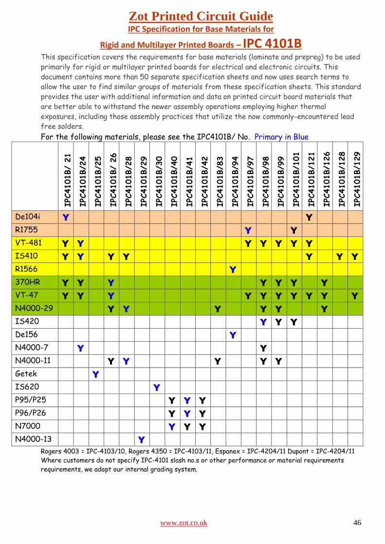
For the following materials, please see the IPC4101B/ No. Primary in Blue
IPC
4101B/
21
IPC
4101B/2
4
IPC
4101B/2
5
IPC
4101B/
26
IPC
4101B/2
8
IPC
4101B/2
9
IPC
4101B/3
0
IPC
4101B/4
0
IPC
4101B/4
1
IPC
4101B/4
2
IPC
4101B/8
3
IPC
4101B/9
4
IPC
4101B/9
7
IPC
4101B/9
8
IPC
4101B/9
9
IPC
4101B/1
01
IPC
4101B/1
21
IPC
4101B/1
26
IPC
4101B/1
28
IPC
4101B/1
29
De104i Y Y
R1755 Y Y
VT-481 Y Y Y Y Y Y Y
IS410 Y Y Y Y Y Y Y
R1566 Y
370HR Y Y Y Y Y Y Y
VT-47 Y Y Y Y Y Y Y Y Y Y
N4000-29 Y Y Y Y Y Y
IS420 Y Y Y
De156 Y
N4000-7 Y Y
N4000-11 Y Y Y Y Y
Getek Y
IS620 Y
P95/P25 Y Y Y
P96/P26 Y Y Y
N7000 Y Y Y
N4000-13 Y
Rogers 4003 = IPC-4103/10, Rogers 4350 = IPC-4103/11, Espanex = IPC-4204/11 Dupont = IPC-4204/11
Where customers do not specify IPC-4101 slash no.s or other performance or material requirements
requirements, we adopt our internal grading system.
Zot Printed Circuit Guide
www.zot.co.uk 47
Complex Printed Circuits How are these made At Zot we manufacture from the smallest simplest 1 layer single sided board to complex large
20 layer plus boards with multiple ball grid arrays etc…..
It is obvious that the simplest of pcb manufacturing processes can produce simple single sided
boards, however in order to manufacture large complex 20 layer plus designs, we need to ensure
that we are using state of the art advanced manufacturing equipment and production
techniques.
All products manufactured by Zot, are initially engineered for manufacture, and grouped into
levels for manufacturability, which then decides what processes will be applied to what level of
product complexity.
Examples are as follows
Circuit Imaging – Innerlayer and outerlayer
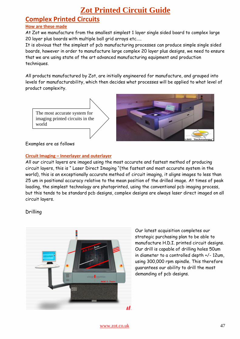
All our circuit layers are imaged using the most accurate and fastest method of producing
circuit layers, this is “ Laser Direct Imaging “(the fastest and most accurate system in the
world), this is an exceptionally accurate method of circuit imaging, it aligns images to less than
25 um in positional accuracy relative to the mean position of the drilled image. At times of peak
loading, the simplest technology are photoprinted, using the conventional pcb imaging process,
but this tends to be standard pcb designs, complex designs are always laser direct imaged on all
circuit layers.
Drilling
Our latest acquisition completes our
strategic purchasing plan to be able to
manufacture H.D.I. printed circuit designs.
Our drill is capable of drilling holes 50um
in diameter to a controlled depth +/- 12um,
using 300,000 rpm spindle. This therefore
guarantees our ability to drill the most
demanding of pcb designs.
The most accurate system for
imaging printed circuits in the
world
Zot Printed Circuit Guide
www.zot.co.uk 48
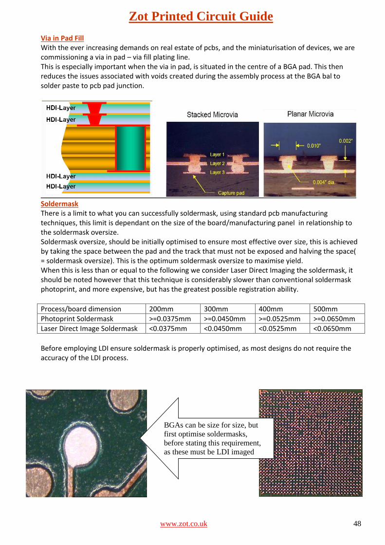
Via in Pad Fill With the ever increasing demands on real estate of pcbs, and the miniaturisation of devices, we are commissioning a via in pad – via fill plating line. This is especially important when the via in pad, is situated in the centre of a BGA pad. This then reduces the issues associated with voids created during the assembly process at the BGA bal to solder paste to pcb pad junction.
Soldermask There is a limit to what you can successfully soldermask, using standard pcb manufacturing techniques, this limit is dependant on the size of the board/manufacturing panel in relationship to the soldermask oversize. Soldermask oversize, should be initially optimised to ensure most effective over size, this is achieved by taking the space between the pad and the track that must not be exposed and halving the space( = soldermask oversize). This is the optimum soldermask oversize to maximise yield. When this is less than or equal to the following we consider Laser Direct Imaging the soldermask, it should be noted however that this technique is considerably slower than conventional soldermask photoprint, and more expensive, but has the greatest possible registration ability.
Process/board dimension 200mm 300mm 400mm 500mm
Photoprint Soldermask >=0.0375mm >=0.0450mm >=0.0525mm >=0.0650mm
Laser Direct Image Soldermask <0.0375mm <0.0450mm <0.0525mm <0.0650mm
Before employing LDI ensure soldermask is properly optimised, as most designs do not require the accuracy of the LDI process.
BGAs can be size for size, but
first optimise soldermasks,
before stating this requirement,
as these must be LDI imaged
Zot Printed Circuit Guide
www.zot.co.uk 49
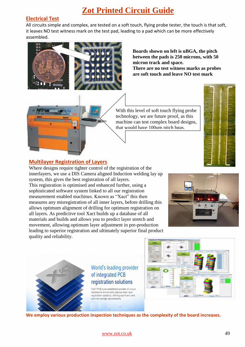
Electrical Test All circuits simple and complex, are tested on a soft touch, flying probe tester, the touch is that soft, it leaves NO test witness mark on the test pad, leading to a pad which can be more effectively assembled.
We employ various production inspection techniques as the complexity of the board increases.
Boards shown on left is uBGA, the pitch
between the pads is 250 microns, with 50
micron track and space.
There are no test witness marks as probes
are soft touch and leave NO test mark
With this level of soft touch flying probe
technology, we are future proof, as this
machine can test complex board designs,
that would have 100um pitch bgas.
Multilayer Registration of Layers Where designs require tighter control of the registration of the
innerlayers, we use a DIS Camera aligned Induction welding lay up
system, this gives the best registration of all layers.
This registration is optimised and enhanced further, using a
sophisticated software system linked to all our registration
measurement enabled machines. Known as “Xact” this then
measures any misregistration of all inner layers, before drilling this
allows optimum alignment of drilling for optimum registration on
all layers. As predictive tool Xact builds up a database of all
materials and builds and allows you to predict layer stretch and
movement, allowing optimum layer adjustment in pre-production
leading to superior registration and ultimately superior final product
quality and reliability.
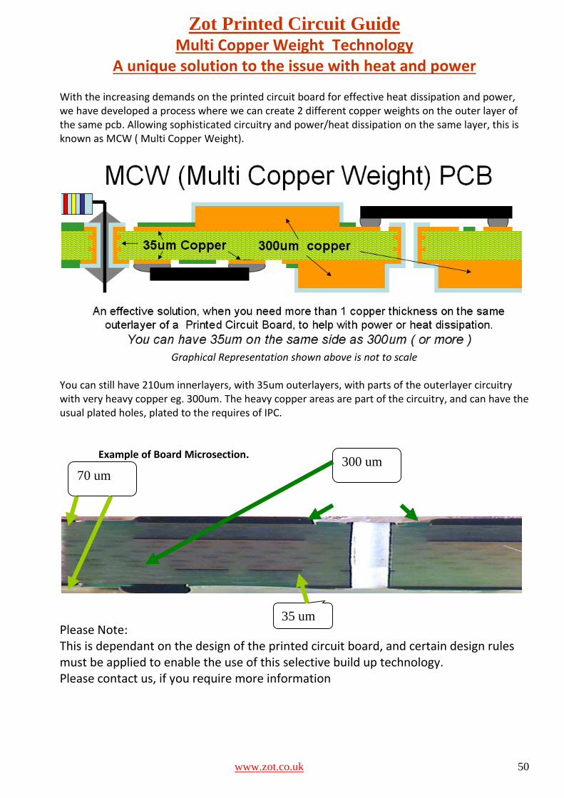
Zot Printed Circuit Guide
www.zot.co.uk 50
Multi Copper Weight Technology A unique solution to the issue with heat and power
With the increasing demands on the printed circuit board for effective heat dissipation and power, we have developed a process where we can create 2 different copper weights on the outer layer of the same pcb. Allowing sophisticated circuitry and power/heat dissipation on the same layer, this is known as MCW ( Multi Copper Weight).
Graphical Representation shown above is not to scale
You can still have 210um innerlayers, with 35um outerlayers, with parts of the outerlayer circuitry with very heavy copper eg. 300um. The heavy copper areas are part of the circuitry, and can have the usual plated holes, plated to the requires of IPC. Example of Board Microsection.
Please Note: This is dependant on the design of the printed circuit board, and certain design rules must be applied to enable the use of this selective build up technology. Please contact us, if you require more information
300 um 70 um
35 um
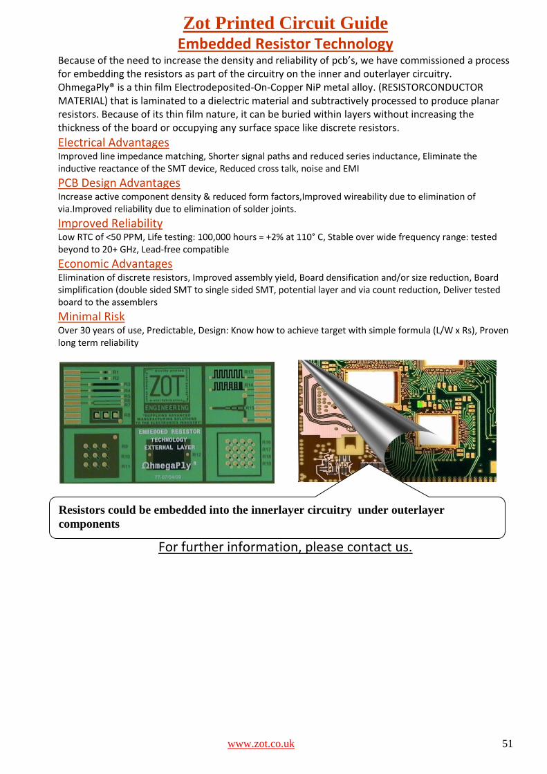
Zot Printed Circuit Guide
www.zot.co.uk 51
Embedded Resistor Technology Because of the need to increase the density and reliability of pcb’s, we have commissioned a process for embedding the resistors as part of the circuitry on the inner and outerlayer circuitry. OhmegaPly® is a thin film Electrodeposited-On-Copper NiP metal alloy. (RESISTORCONDUCTOR MATERIAL) that is laminated to a dielectric material and subtractively processed to produce planar resistors. Because of its thin film nature, it can be buried within layers without increasing the thickness of the board or occupying any surface space like discrete resistors.
Electrical Advantages Improved line impedance matching, Shorter signal paths and reduced series inductance, Eliminate the inductive reactance of the SMT device, Reduced cross talk, noise and EMI
PCB Design Advantages Increase active component density & reduced form factors,Improved wireability due to elimination of via.Improved reliability due to elimination of solder joints.
Improved Reliability Low RTC of <50 PPM, Life testing: 100,000 hours = +2% at 110° C, Stable over wide frequency range: tested beyond to 20+ GHz, Lead-free compatible
Economic Advantages Elimination of discrete resistors, Improved assembly yield, Board densification and/or size reduction, Board simplification (double sided SMT to single sided SMT, potential layer and via count reduction, Deliver tested board to the assemblers
Minimal Risk Over 30 years of use, Predictable, Design: Know how to achieve target with simple formula (L/W x Rs), Proven long term reliability
For further information, please contact us.
Resistors could be embedded into the innerlayer circuitry under outerlayer
components
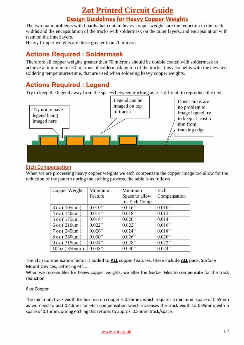
Zot Printed Circuit Guide
www.zot.co.uk 52
Design Guidelines for Heavy Copper Weights The two main problems with boards that contain heavy copper weights are the reduction in the track
widths and the encapsulation of the tracks with soldermask on the outer layers, and encapsulation with
resin on the innerlayers.
Heavy Copper weights are those greater than 70 micron
Actions Required : Soldermask Therefore all copper weights greater than 70 microns should be double coated with soldermask to
achieve a minimum of 50 microns of soldermask on top of the tracks, this also helps with the elevated
soldering temperatures/time, that are used when soldering heavy copper weights.
Actions Required : Legend Try to keep the legend away from the spaces between tracking as it is difficult to reproduce the text.
Etch Compensation When we are processing heavy copper weights we etch compensate the copper image too allow for the
reduction of the pattern during the etching process, the table is as follows
Copper Weight Minimum
Feature
Minimum
Space to allow
for Etch Comp.
Etch
Compensation
3 oz ( 105um ) 0.010” 0.016” 0.010”
4 oz ( 140um ) 0.014” 0.018” 0.012”
5 oz ( 175um ) 0.018” 0.020” 0.014”
6 oz ( 210um ) 0.022” 0.022” 0.016”
7 oz ( 245um ) 0.026” 0.024” 0.018”
8 oz ( 280um ) 0.030” 0.026” 0.020”
9 oz ( 315um ) 0.034” 0.028” 0.022”
10 oz ( 350um ) 0.038” 0.030” 0.024”
The Etch Compensation factor is added to ALL copper features, these include ALL pads, Surface Mount Devices, Lettering etc… When we receive files for heavy copper weights, we alter the Gerber Files to compensate for the track reduction.
6 oz Copper
The minimum track width for 6oz micron copper is 0.55mm, which requires a minimum space of 0.55mm as we need to add 0.40mm for etch compensation which increases the track width to 0.95mm, with a space of 0.15mm, during etching this returns to approx. 0.55mm track/space.
Try not to have
legend being
imaged here
Legend can be
imaged on top
of tracks
Opens areas are
no problem to
image legend try
to keep at least 5
mm from
tracking edge
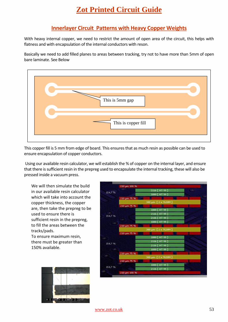
Zot Printed Circuit Guide
www.zot.co.uk 53
Innerlayer Circuit Patterns with Heavy Copper Weights
With heavy internal copper, we need to restrict the amount of open area of the circuit, this helps with flatness and with encapsulation of the internal conductors with reson.
Basically we need to add filled planes to areas between tracking, try not to have more than 5mm of open bare laminate. See Below
This copper fill is 5 mm from edge of board. This ensures that as much resin as possible can be used to ensure encapsulation of copper conductors.
Using our available resin calculator, we will establish the % of copper on the internal layer, and ensure that there is sufficient resin in the prepreg used to encapsulate the internal tracking, these will also be pressed inside a vacuum press.
We will then simulate the build in our available resin calculator which will take into account the copper thickness, the copper are, then take the prepreg to be used to ensure there is sufficient resin in the prepreg, to fill the areas between the tracks/pads. To ensure maximum resin, there must be greater than 150% available.
This is 5mm gap
This is copper fill
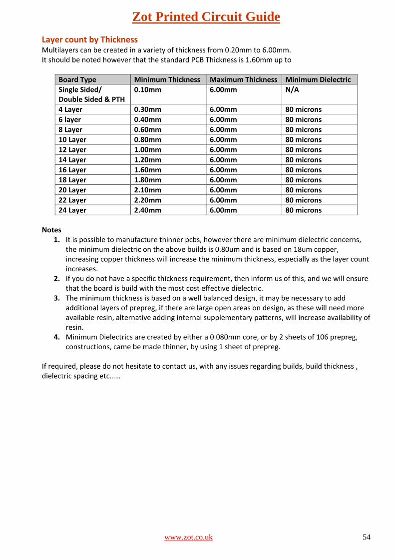
Zot Printed Circuit Guide
www.zot.co.uk 54
Layer count by Thickness Multilayers can be created in a variety of thickness from 0.20mm to 6.00mm. It should be noted however that the standard PCB Thickness is 1.60mm up to
Board Type Minimum Thickness Maximum Thickness Minimum Dielectric
Single Sided/ Double Sided & PTH
0.10mm 6.00mm N/A
4 Layer 0.30mm 6.00mm 80 microns
6 layer 0.40mm 6.00mm 80 microns
8 Layer 0.60mm 6.00mm 80 microns
10 Layer 0.80mm 6.00mm 80 microns
12 Layer 1.00mm 6.00mm 80 microns
14 Layer 1.20mm 6.00mm 80 microns
16 Layer 1.60mm 6.00mm 80 microns
18 Layer 1.80mm 6.00mm 80 microns
20 Layer 2.10mm 6.00mm 80 microns
22 Layer 2.20mm 6.00mm 80 microns
24 Layer 2.40mm 6.00mm 80 microns
Notes
1. It is possible to manufacture thinner pcbs, however there are minimum dielectric concerns, the minimum dielectric on the above builds is 0.80um and is based on 18um copper, increasing copper thickness will increase the minimum thickness, especially as the layer count increases.
2. If you do not have a specific thickness requirement, then inform us of this, and we will ensure that the board is build with the most cost effective dielectric.
3. The minimum thickness is based on a well balanced design, it may be necessary to add additional layers of prepreg, if there are large open areas on design, as these will need more available resin, alternative adding internal supplementary patterns, will increase availability of resin.
4. Minimum Dielectrics are created by either a 0.080mm core, or by 2 sheets of 106 prepreg, constructions, came be made thinner, by using 1 sheet of prepreg.
If required, please do not hesitate to contact us, with any issues regarding builds, build thickness , dielectric spacing etc……
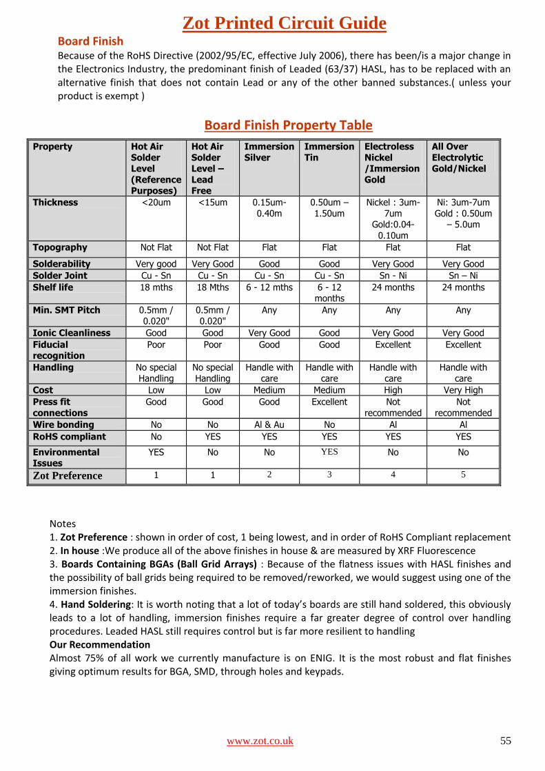
Zot Printed Circuit Guide
www.zot.co.uk 55
Property Hot Air
Solder Level
(Reference
Purposes)
Hot Air
Solder Level –
Lead
Free
Immersion
Silver Immersion
Tin Electroless
Nickel /Immersion
Gold
All Over
Electrolytic Gold/Nickel
Thickness <20um <15um 0.15um-
0.40m
0.50um –
1.50um
Nickel : 3um-
7um Gold:0.04-
0.10um
Ni: 3um-7um
Gold : 0.50um – 5.0um
Topography Not Flat Not Flat Flat Flat Flat Flat
Solderability Very good Very Good Good Good Very Good Very Good
Solder Joint Cu - Sn Cu - Sn Cu - Sn Cu - Sn Sn - Ni Sn – Ni
Shelf life 18 mths 18 Mths 6 - 12 mths 6 - 12 months
24 months 24 months
Min. SMT Pitch 0.5mm /
0.020"
0.5mm /
0.020"
Any Any Any Any
Ionic Cleanliness Good Good Very Good Good Very Good Very Good
Fiducial recognition
Poor Poor Good Good Excellent Excellent
Handling No special
Handling
No special
Handling
Handle with
care
Handle with
care
Handle with
care
Handle with
care
Cost Low Low Medium Medium High Very High
Press fit
connections Good Good Good Excellent Not
recommended
Not
recommended
Wire bonding No No Al & Au No Al Al
RoHS compliant No YES YES YES YES YES
Environmental Issues
YES No No YES No No
Zot Preference 1 1 2 3 4 5
Board Finish Because of the RoHS Directive (2002/95/EC, effective July 2006), there has been/is a major change in the Electronics Industry, the predominant finish of Leaded (63/37) HASL, has to be replaced with an alternative finish that does not contain Lead or any of the other banned substances.( unless your product is exempt )
Board Finish Property Table
Notes 1. Zot Preference : shown in order of cost, 1 being lowest, and in order of RoHS Compliant replacement 2. In house :We produce all of the above finishes in house & are measured by XRF Fluorescence 3. Boards Containing BGAs (Ball Grid Arrays) : Because of the flatness issues with HASL finishes and the possibility of ball grids being required to be removed/reworked, we would suggest using one of the immersion finishes. 4. Hand Soldering: It is worth noting that a lot of today’s boards are still hand soldered, this obviously leads to a lot of handling, immersion finishes require a far greater degree of control over handling procedures. Leaded HASL still requires control but is far more resilient to handling Our Recommendation Almost 75% of all work we currently manufacture is on ENIG. It is the most robust and flat finishes giving optimum results for BGA, SMD, through holes and keypads.
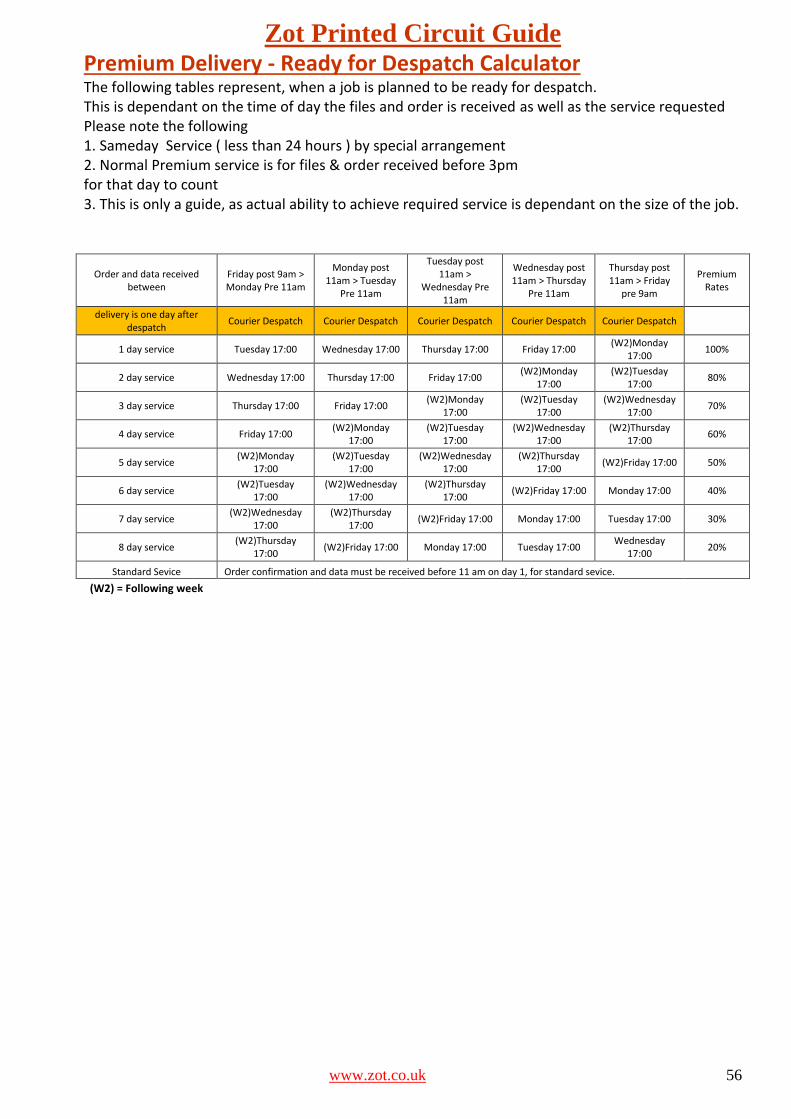
Zot Printed Circuit Guide
www.zot.co.uk 56
Premium Delivery - Ready for Despatch Calculator The following tables represent, when a job is planned to be ready for despatch. This is dependant on the time of day the files and order is received as well as the service requested Please note the following 1. Sameday Service ( less than 24 hours ) by special arrangement 2. Normal Premium service is for files & order received before 3pm for that day to count 3. This is only a guide, as actual ability to achieve required service is dependant on the size of the job.
Order and data received between
Friday post 9am > Monday Pre 11am
Monday post 11am > Tuesday
Pre 11am
Tuesday post 11am >
Wednesday Pre 11am
Wednesday post 11am > Thursday
Pre 11am
Thursday post 11am > Friday
pre 9am
Premium Rates
delivery is one day after despatch
Courier Despatch Courier Despatch Courier Despatch Courier Despatch Courier Despatch
1 day service Tuesday 17:00 Wednesday 17:00 Thursday 17:00 Friday 17:00 (W2)Monday
17:00 100%
2 day service Wednesday 17:00 Thursday 17:00 Friday 17:00 (W2)Monday
17:00 (W2)Tuesday
17:00 80%
3 day service Thursday 17:00 Friday 17:00 (W2)Monday
17:00 (W2)Tuesday
17:00 (W2)Wednesday
17:00 70%
4 day service Friday 17:00 (W2)Monday
17:00 (W2)Tuesday
17:00 (W2)Wednesday
17:00 (W2)Thursday
17:00 60%
5 day service (W2)Monday
17:00 (W2)Tuesday
17:00 (W2)Wednesday
17:00 (W2)Thursday
17:00 (W2)Friday 17:00 50%
6 day service (W2)Tuesday
17:00 (W2)Wednesday
17:00 (W2)Thursday
17:00 (W2)Friday 17:00 Monday 17:00 40%
7 day service (W2)Wednesday
17:00 (W2)Thursday
17:00 (W2)Friday 17:00 Monday 17:00 Tuesday 17:00 30%
8 day service (W2)Thursday
17:00 (W2)Friday 17:00 Monday 17:00 Tuesday 17:00
Wednesday 17:00
20%
Standard Sevice Order confirmation and data must be received before 11 am on day 1, for standard sevice.
(W2) = Following week
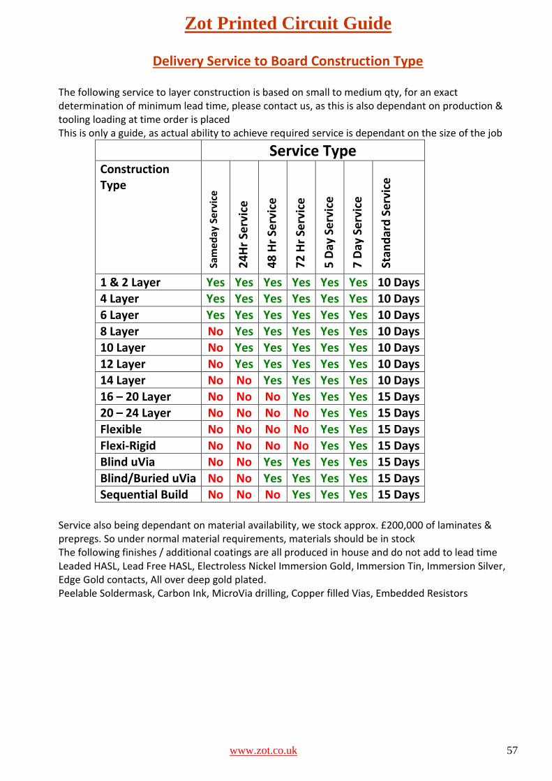
Zot Printed Circuit Guide
www.zot.co.uk 57
Delivery Service to Board Construction Type The following service to layer construction is based on small to medium qty, for an exact determination of minimum lead time, please contact us, as this is also dependant on production & tooling loading at time order is placed This is only a guide, as actual ability to achieve required service is dependant on the size of the job
Service Type Construction Type
Sam
eday
Ser
vice
24
Hr
Serv
ice
48
Hr
Serv
ice
72
Hr
Serv
ice
5 D
ay S
erv
ice
7 D
ay S
erv
ice
Stan
dar
d S
erv
ice
1 & 2 Layer Yes Yes Yes Yes Yes Yes 10 Days 4 Layer Yes Yes Yes Yes Yes Yes 10 Days
6 Layer Yes Yes Yes Yes Yes Yes 10 Days
8 Layer No Yes Yes Yes Yes Yes 10 Days 10 Layer No Yes Yes Yes Yes Yes 10 Days
12 Layer No Yes Yes Yes Yes Yes 10 Days 14 Layer No No Yes Yes Yes Yes 10 Days
16 – 20 Layer No No No Yes Yes Yes 15 Days 20 – 24 Layer No No No No Yes Yes 15 Days
Flexible No No No No Yes Yes 15 Days
Flexi-Rigid No No No No Yes Yes 15 Days Blind uVia No No Yes Yes Yes Yes 15 Days
Blind/Buried uVia No No Yes Yes Yes Yes 15 Days Sequential Build No No No Yes Yes Yes 15 Days
Service also being dependant on material availability, we stock approx. £200,000 of laminates & prepregs. So under normal material requirements, materials should be in stock The following finishes / additional coatings are all produced in house and do not add to lead time Leaded HASL, Lead Free HASL, Electroless Nickel Immersion Gold, Immersion Tin, Immersion Silver, Edge Gold contacts, All over deep gold plated. Peelable Soldermask, Carbon Ink, MicroVia drilling, Copper filled Vias, Embedded Resistors
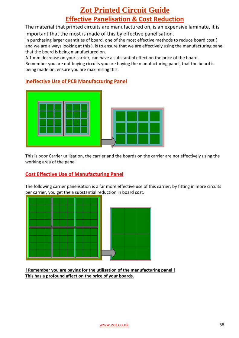
Zot Printed Circuit Guide
www.zot.co.uk 58
Effective Panelisation & Cost Reduction The material that printed circuits are manufactured on, is an expensive laminate, it is important that the most is made of this by effective panelisation. In purchasing larger quantities of board, one of the most effective methods to reduce board cost ( and we are always looking at this ), is to ensure that we are effectively using the manufacturing panel that the board is being manufactured on. A 1 mm decrease on your carrier, can have a substantial effect on the price of the board. Remember you are not buying circuits you are buying the manufacturing panel, that the board is being made on, ensure you are maximising this.
Ineffective Use of PCB Manufacturing Panel
This is poor Carrier utilisation, the carrier and the boards on the carrier are not effectively using the working area of the panel
Cost Effective Use of Manufacturing Panel The following carrier panelisation is a far more effective use of this carrier, by fitting in more circuits per carrier, you get the a substantial reduction in board cost.
! Remember you are paying for the utilisation of the manufacturing panel ! This has a profound affect on the price of your boards.
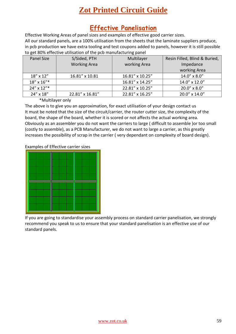
Zot Printed Circuit Guide
www.zot.co.uk 59
Effective Panelisation Effective Working Areas of panel sizes and examples of effective good carrier sizes. All our standard panels, are a 100% utilisation from the sheets that the laminate suppliers produce, in pcb production we have extra tooling and test coupons added to panels, however it is still possible to get 80% effective utilisation of the pcb manufacturing panel
Panel Size S/Sided, PTH Working Area
Multilayer working Area
Resin Filled, Blind & Buried, Impedance
working Area
18” x 12” 16.81” x 10.81 16.81” x 10.25” 14.0” x 8.0”
18” x 16”* 16.81” x 14.25” 14.0” x 12.0”
24” x 12”* 22.81” x 10.25” 20.0” x 8.0”
24” x 18” 22.81” x 16.81” 22.81” x 16.25” 20.0” x 14.0”
*Multilayer only The above is to give you an approximation, for exact utilisation of your design contact us It must be noted that the size of the circuit/carrier, the router cutter size, the complexity of the board, the shape of the board, whether it is scored or not affects the actual working area. Obviously as an assembler you do not want the carriers to large ( difficult to assemble )or too small (costly to assemble), as a PCB Manufacturer, we do not want to large a carrier, as this greatly increases the possibility of scrap in the carrier ( very dependant on complexity of board design). Examples of Effective carrier sizes
If you are going to standardise your assembly process on standard carrier panelisation, we strongly recommend you speak to us to ensure that your standard panelisation is an effective use of our standard panels.

Zot Printed Circuit Guide
www.zot.co.uk 60
Default Specification We supply to a vast range of companies, from very large OEM/CEM to very small ( and just as important ) users of printed circuits. Because not all of our customers fully understand the various specifications regarding print circuit boards, we have a standard set of defaults. If you do not specify the following requirement, we will quote/manufacture using the following. This will be stated on the quotation. Board Thickness = 1.60mm +/- 10%. Laminate Type = First Grade Lead free Compatible Laminate Copper Weight = 35um Inners and Outers Build = Zot Standard Build ( can be altered dependant on board design ) Soldermask Colour = Green Legend Colour = White Single Circuits ( unless requested by default to panelise or panelisation requested ) Finish = Lead free HASL Edge Gold Finger plating = Minimum of 1.50um, Nickel minimum of 3um. Inspection to I.P.C. 600 Class 2.
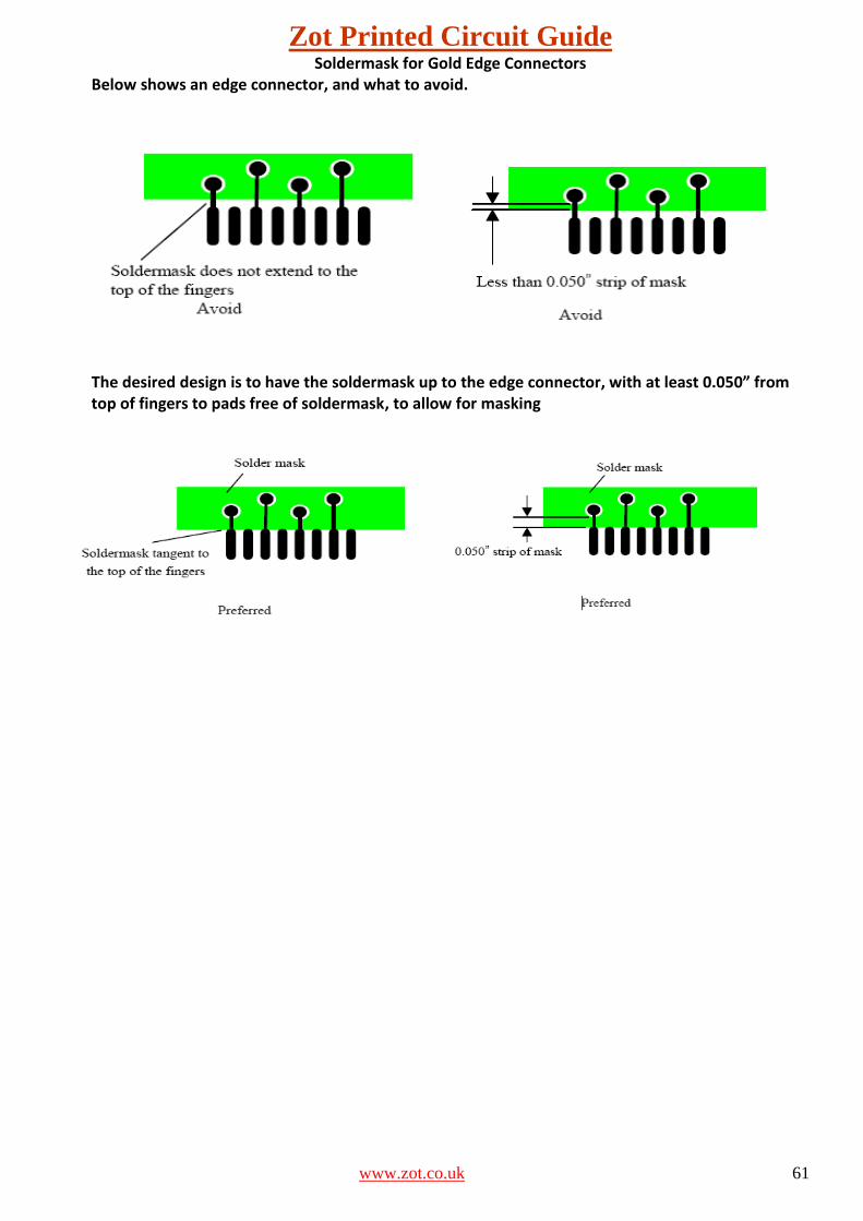
Zot Printed Circuit Guide
www.zot.co.uk 61
Soldermask for Gold Edge Connectors Below shows an edge connector, and what to avoid.
The desired design is to have the soldermask up to the edge connector, with at least 0.050” from top of fingers to pads free of soldermask, to allow for masking
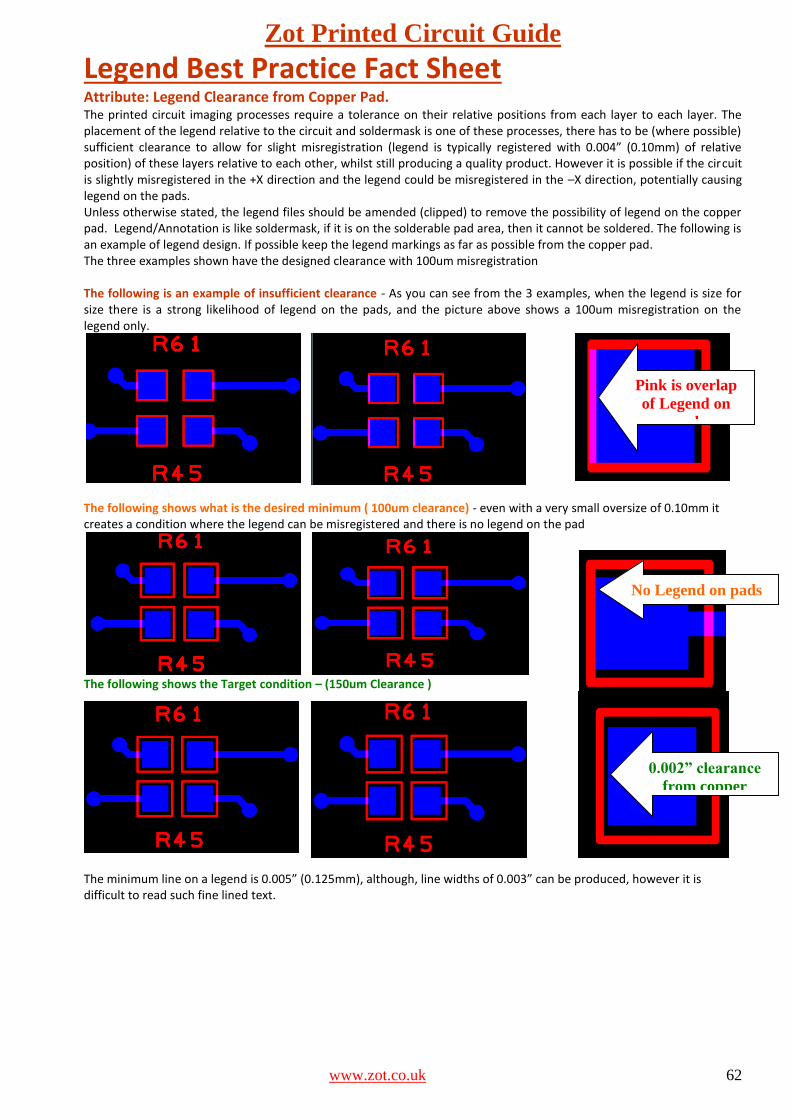
Zot Printed Circuit Guide
www.zot.co.uk 62
Legend Best Practice Fact Sheet Attribute: Legend Clearance from Copper Pad. The printed circuit imaging processes require a tolerance on their relative positions from each layer to each layer. The placement of the legend relative to the circuit and soldermask is one of these processes, there has to be (where possible) sufficient clearance to allow for slight misregistration (legend is typically registered with 0.004” (0.10mm) of relative position) of these layers relative to each other, whilst still producing a quality product. However it is possible if the circuit is slightly misregistered in the +X direction and the legend could be misregistered in the –X direction, potentially causing legend on the pads. Unless otherwise stated, the legend files should be amended (clipped) to remove the possibility of legend on the copper pad. Legend/Annotation is like soldermask, if it is on the solderable pad area, then it cannot be soldered. The following is an example of legend design. If possible keep the legend markings as far as possible from the copper pad. The three examples shown have the designed clearance with 100um misregistration The following is an example of insufficient clearance - As you can see from the 3 examples, when the legend is size for size there is a strong likelihood of legend on the pads, and the picture above shows a 100um misregistration on the legend only.
The following shows what is the desired minimum ( 100um clearance) - even with a very small oversize of 0.10mm it creates a condition where the legend can be misregistered and there is no legend on the pad
The following shows the Target condition – (150um Clearance ) The minimum line on a legend is 0.005” (0.125mm), although, line widths of 0.003” can be produced, however it is difficult to read such fine lined text.
Pink is overlap
of Legend on
pad
No Legend on pads
0.002” clearance
from copper
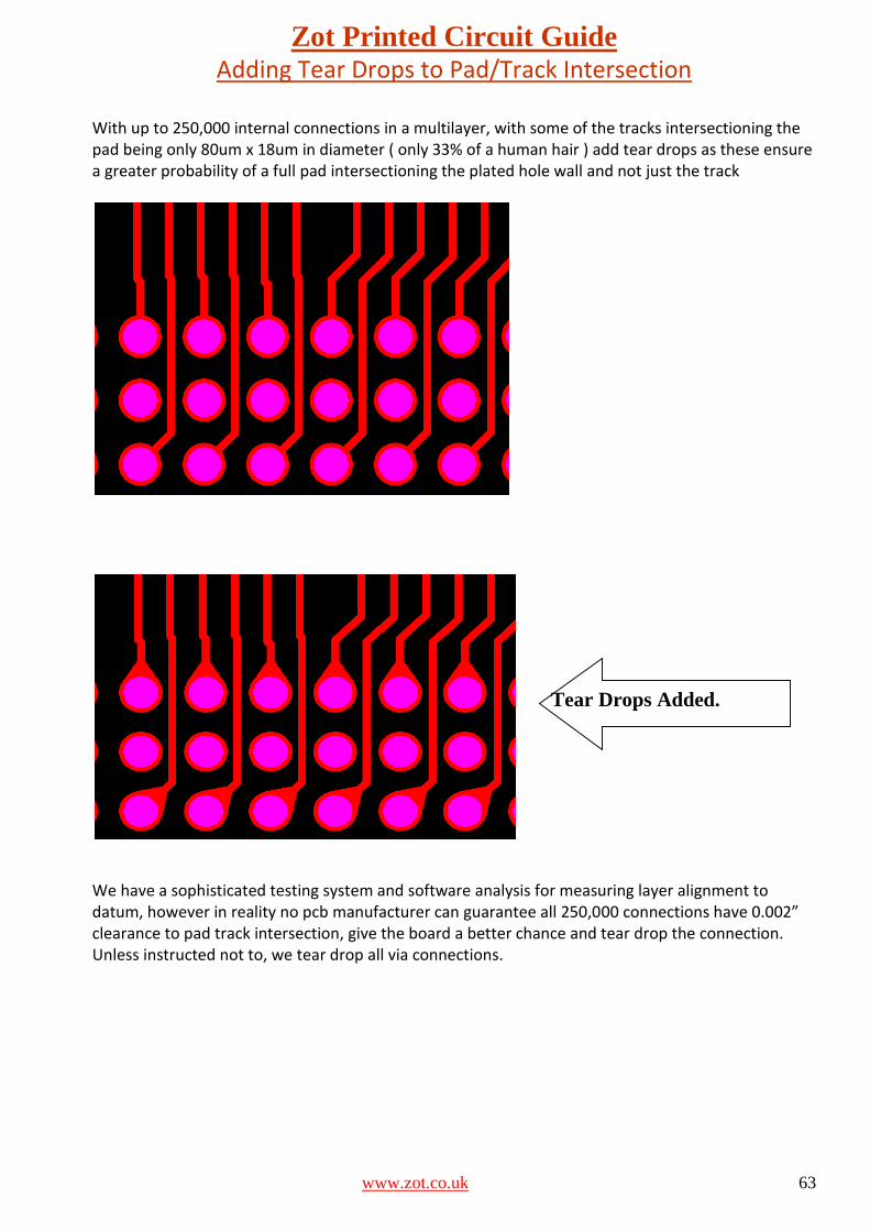
Zot Printed Circuit Guide
www.zot.co.uk 63
Adding Tear Drops to Pad/Track Intersection
With up to 250,000 internal connections in a multilayer, with some of the tracks intersectioning the pad being only 80um x 18um in diameter ( only 33% of a human hair ) add tear drops as these ensure a greater probability of a full pad intersectioning the plated hole wall and not just the track
We have a sophisticated testing system and software analysis for measuring layer alignment to datum, however in reality no pcb manufacturer can guarantee all 250,000 connections have 0.002” clearance to pad track intersection, give the board a better chance and tear drop the connection. Unless instructed not to, we tear drop all via connections.
Tear Drops Added.
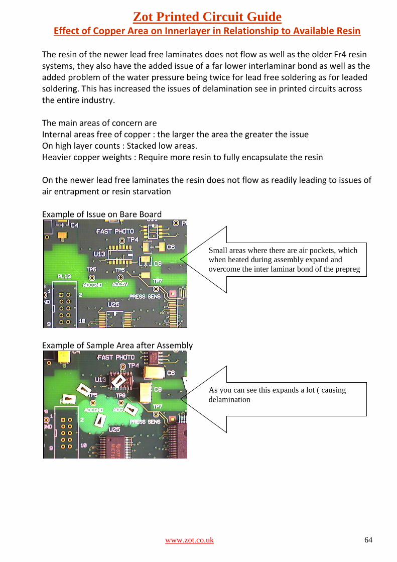
Zot Printed Circuit Guide
www.zot.co.uk 64
Effect of Copper Area on Innerlayer in Relationship to Available Resin The resin of the newer lead free laminates does not flow as well as the older Fr4 resin systems, they also have the added issue of a far lower interlaminar bond as well as the added problem of the water pressure being twice for lead free soldering as for leaded soldering. This has increased the issues of delamination see in printed circuits across the entire industry. The main areas of concern are Internal areas free of copper : the larger the area the greater the issue On high layer counts : Stacked low areas. Heavier copper weights : Require more resin to fully encapsulate the resin On the newer lead free laminates the resin does not flow as readily leading to issues of air entrapment or resin starvation Example of Issue on Bare Board
Example of Sample Area after Assembly
Small areas where there are air pockets, which
when heated during assembly expand and
overcome the inter laminar bond of the prepreg
As you can see this expands a lot ( causing
delamination
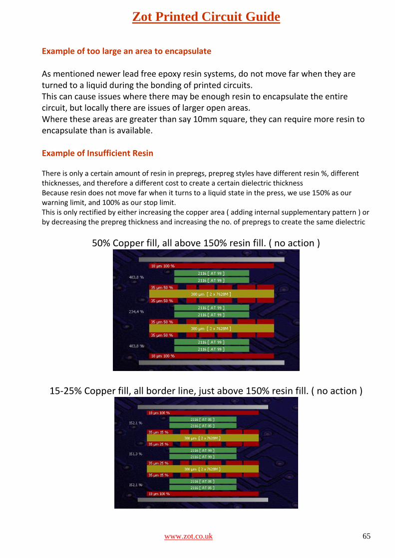
Zot Printed Circuit Guide
www.zot.co.uk 65
Example of too large an area to encapsulate As mentioned newer lead free epoxy resin systems, do not move far when they are turned to a liquid during the bonding of printed circuits. This can cause issues where there may be enough resin to encapsulate the entire circuit, but locally there are issues of larger open areas. Where these areas are greater than say 10mm square, they can require more resin to encapsulate than is available.
Example of Insufficient Resin There is only a certain amount of resin in prepregs, prepreg styles have different resin %, different thicknesses, and therefore a different cost to create a certain dielectric thickness Because resin does not move far when it turns to a liquid state in the press, we use 150% as our warning limit, and 100% as our stop limit. This is only rectified by either increasing the copper area ( adding internal supplementary pattern ) or by decreasing the prepreg thickness and increasing the no. of prepregs to create the same dielectric
50% Copper fill, all above 150% resin fill. ( no action )
15-25% Copper fill, all border line, just above 150% resin fill. ( no action )

Zot Printed Circuit Guide
www.zot.co.uk 66
5% Copper fill, all failed, below 150% resin fill. ( ACTION REQUIRED )
Zot Printed Circuit Guide
www.zot.co.uk 67
Supplementary Patterns This is the additional of copper patterns to the internal and external layers, these are non functional but they will increases both yields of board manufacturer, and at the assembly of product. Supplementary patterns are only added to boards where the customer has given a global authorisation, otherwise permission is applied on a job by job basis.
Internal Supplementary Patterns – Solid is Best The main purpose of these, is by increasing the copper in the isolated layers, it then increases the availability of the resin from the prepreg to encapsulate the innerlayer circuitry. Which can reduce issues with blistering, Delamination, air voids, low areas, foil wrinkling.
We can add this to your layers, and will gave a clearance of 2mm ( 0.080” ) from copper circuitry or holes. Using solid copper as fill, ensures maximum availability of prepreg, and also less issues with AOI of layers.
Because there is not a lot of copper
on layers 3 & 4, it requires more
prepreg to fill gap between layers,
leading to a possibility of low spots
or voids
By adding internal supplementary
patterns, you decrease the
possibility of low spots and
increase the available resin,
thereby making the board a more
reliable build
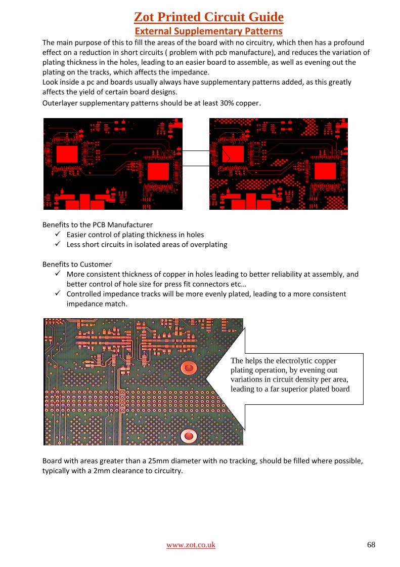
Zot Printed Circuit Guide
www.zot.co.uk 68
External Supplementary Patterns The main purpose of this to fill the areas of the board with no circuitry, which then has a profound effect on a reduction in short circuits ( problem with pcb manufacture), and reduces the variation of plating thickness in the holes, leading to an easier board to assemble, as well as evening out the plating on the tracks, which affects the impedance. Look inside a pc and boards usually always have supplementary patterns added, as this greatly affects the yield of certain board designs.
Outerlayer supplementary patterns should be at least 30% copper.
Benefits to the PCB Manufacturer
Easier control of plating thickness in holes Less short circuits in isolated areas of overplating
Benefits to Customer
More consistent thickness of copper in holes leading to better reliability at assembly, and better control of hole size for press fit connectors etc…
Controlled impedance tracks will be more evenly plated, leading to a more consistent impedance match.
Board with areas greater than a 25mm diameter with no tracking, should be filled where possible, typically with a 2mm clearance to circuitry.
The helps the electrolytic copper
plating operation, by evening out
variations in circuit density per area,
leading to a far superior plated board
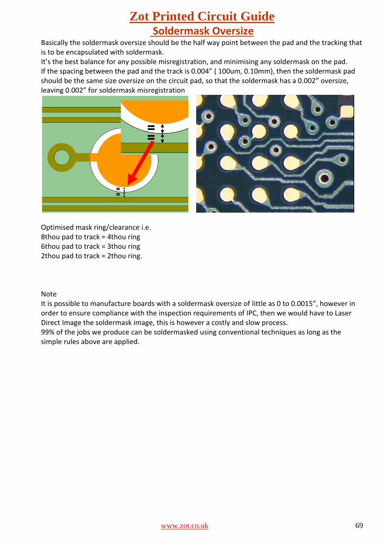
Zot Printed Circuit Guide
www.zot.co.uk 69
Soldermask Oversize Basically the soldermask oversize should be the half way point between the pad and the tracking that is to be encapsulated with soldermask. It’s the best balance for any possible misregistration, and minimising any soldermask on the pad. If the spacing between the pad and the track is 0.004” ( 100um, 0.10mm), then the soldermask pad should be the same size oversize on the circuit pad, so that the soldermask has a 0.002” oversize, leaving 0.002” for soldermask misregistration
Optimised mask ring/clearance i.e. 8thou pad to track = 4thou ring 6thou pad to track = 3thou ring 2thou pad to track = 2thou ring. Note It is possible to manufacture boards with a soldermask oversize of little as 0 to 0.0015”, however in order to ensure compliance with the inspection requirements of IPC, then we would have to Laser Direct Image the soldermask image, this is however a costly and slow process. 99% of the jobs we produce can be soldermasked using conventional techniques as long as the simple rules above are applied.
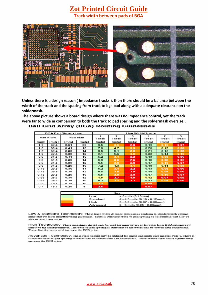
Zot Printed Circuit Guide
www.zot.co.uk 70
Track width between pads of BGA
Unless there is a design reason ( Impedance tracks ), then there should be a balance between the width of the track and the spacing from track to bga pad along with a adequate clearance on the soldermask. The above picture shows a board design where there was no impedance control, yet the track were far to wide in comparison to both the track to pad spacing and the soldermask oversize..
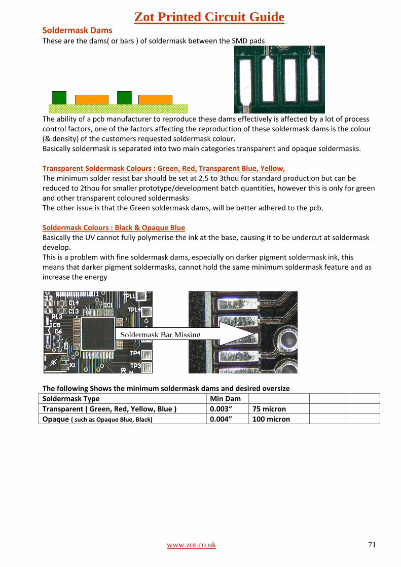
Zot Printed Circuit Guide
www.zot.co.uk 71
Soldermask Dams These are the dams( or bars ) of soldermask between the SMD pads
The ability of a pcb manufacturer to reproduce these dams effectively is affected by a lot of process control factors, one of the factors affecting the reproduction of these soldermask dams is the colour (& density) of the customers requested soldermask colour. Basically soldermask is separated into two main categories transparent and opaque soldermasks. Transparent Soldermask Colours : Green, Red, Transparent Blue, Yellow, The minimum solder resist bar should be set at 2.5 to 3thou for standard production but can be reduced to 2thou for smaller prototype/development batch quantities, however this is only for green and other transparent coloured soldermasks The other issue is that the Green soldermask dams, will be better adhered to the pcb. Soldermask Colours : Black & Opaque Blue Basically the UV cannot fully polymerise the ink at the base, causing it to be undercut at soldermask develop. This is a problem with fine soldermask dams, especially on darker pigment soldermask ink, this means that darker pigment soldermasks, cannot hold the same minimum soldermask feature and as increase the energy
The following Shows the minimum soldermask dams and desired oversize
Soldermask Type Min Dam
Transparent ( Green, Red, Yellow, Blue ) 0.003“ 75 micron
Opaque ( such as Opaque Blue, Black) 0.004” 100 micron
Soldermask Bar Missing
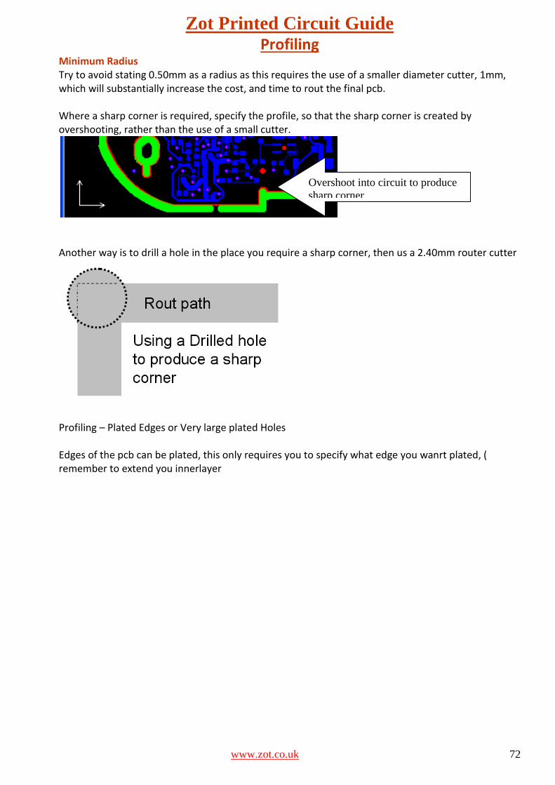
Zot Printed Circuit Guide
www.zot.co.uk 72
Profiling Minimum Radius Try to avoid stating 0.50mm as a radius as this requires the use of a smaller diameter cutter, 1mm, which will substantially increase the cost, and time to rout the final pcb. Where a sharp corner is required, specify the profile, so that the sharp corner is created by overshooting, rather than the use of a small cutter.
Another way is to drill a hole in the place you require a sharp corner, then us a 2.40mm router cutter
Profiling – Plated Edges or Very large plated Holes Edges of the pcb can be plated, this only requires you to specify what edge you wanrt plated, ( remember to extend you innerlayer
Overshoot into circuit to produce
sharp corner

Zot Printed Circuit Guide
www.zot.co.uk 73
ZOT PCB DIVISION PLANT LIST Planning & Estimating PCP2 and Ucam Integrator Computerised estimating/ planning/ shop loading system. 8 workstations networked to 20 shop floor data terminals.
Remote Tooling Site 1 Mania-Barco Ucam Software - 2 Seats
Remote Tooling Site 2 Mania-Barco Ucam Software - 2 Seats
P.C.B. Tooling Department in a Controlled environment Barco BG 7304 Laser photo plotter with scanning facilities Mania-Barco Ucam Software - 5 Seats Barco Auto Fixture Kodak film processor
Drilling & Routering Department
5 off single and twin spindle Automatic Prosys Wessell Drills 3 off Pluritec Single Spindle Automatic Drills 1 off 2 headed Schmoll Depth Drill Drill (2010) 1 off 1 headed Schmoll Depth Drill Drill (2011) 1 off 1 headed Schmoll XRC X-Ray drill (2012) Glenbrook X-ray inspection Equipment 2 off S.E.L. R100-S Router DNC linked EX200 Excellon Drill/Router machine 3 heads DNC linked LHMT SCM411 CNC Scoring Machine (2012)
Multilayer Department Fully Automated cold transfer Luaffer Vacuum Lamination press (2012) Komtek Press DIS PRS 77 L/U Direct Optical Registration Induction welding (2012) Multiline 4 Slot tooling Post Etch Punch Orbotech Discovery AOI – ( 2010) New Custom Build Cleanroom Layup Area (2012) Xact PCB Registration system (2012)
Wet Processes Hollmuller Innerlayer Etch and Resist Strip Line Hollmuller Horizontal Alternative Oxide Line Hollmuller Horizontal Desmear Pola Massa Deburring and power wash (2010) Automated Pattern Plating Line Pulse Plating rectification all copper cells Electrolytic copper via Fill Plating Line (2009) Horizontal Direct Metallisation Line Hollmuller Plating Resist developer and Etch Line Hollmuller Innerlayer Chemical Cleaning Line Various Video Magnification inspection equipment
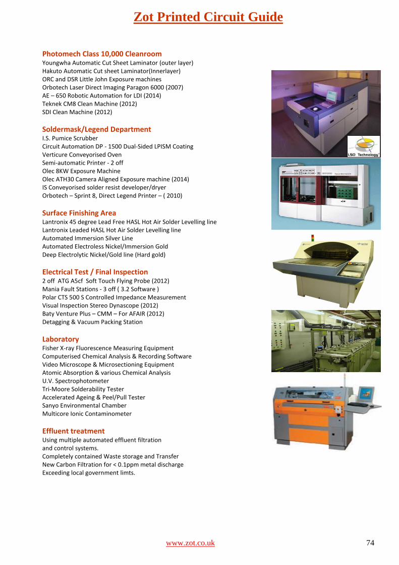
Zot Printed Circuit Guide
www.zot.co.uk 74
Photomech Class 10,000 Cleanroom Youngwha Automatic Cut Sheet Laminator (outer layer) Hakuto Automatic Cut sheet Laminator(Innerlayer) ORC and DSR Little John Exposure machines Orbotech Laser Direct Imaging Paragon 6000 (2007) AE – 650 Robotic Automation for LDI (2014) Teknek CM8 Clean Machine (2012) SDI Clean Machine (2012)
Soldermask/Legend Department I.S. Pumice Scrubber Circuit Automation DP - 1500 Dual-Sided LPISM Coating Verticure Conveyorised Oven Semi-automatic Printer - 2 off Olec 8KW Exposure Machine Olec ATH30 Camera Aligned Exposure machine (2014) IS Conveyorised solder resist developer/dryer Orbotech – Sprint 8, Direct Legend Printer – ( 2010)
Surface Finishing Area Lantronix 45 degree Lead Free HASL Hot Air Solder Levelling line Lantronix Leaded HASL Hot Air Solder Levelling line Automated Immersion Silver Line Automated Electroless Nickel/Immersion Gold Deep Electrolytic Nickel/Gold line (Hard gold)
Electrical Test / Final Inspection 2 off ATG A5cf Soft Touch Flying Probe (2012) Mania Fault Stations - 3 off ( 3.2 Software ) Polar CTS 500 S Controlled Impedance Measurement Visual Inspection Stereo Dynascope (2012) Baty Venture Plus – CMM – For AFAIR (2012) Detagging & Vacuum Packing Station
Laboratory Fisher X-ray Fluorescence Measuring Equipment Computerised Chemical Analysis & Recording Software Video Microscope & Microsectioning Equipment Atomic Absorption & various Chemical Analysis U.V. Spectrophotometer Tri-Moore Solderability Tester Accelerated Ageing & Peel/Pull Tester Sanyo Environmental Chamber Multicore Ionic Contaminometer
Effluent treatment Using multiple automated effluent filtration and control systems. Completely contained Waste storage and Transfer New Carbon Filtration for < 0.1ppm metal discharge Exceeding local government limts.
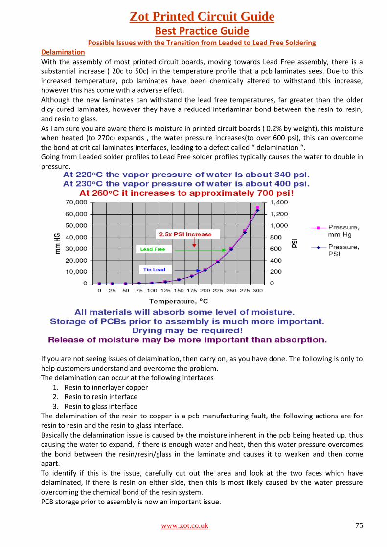
Zot Printed Circuit Guide
www.zot.co.uk 75
Best Practice Guide Possible Issues with the Transition from Leaded to Lead Free Soldering
Delamination With the assembly of most printed circuit boards, moving towards Lead Free assembly, there is a substantial increase ( 20c to 50c) in the temperature profile that a pcb laminates sees. Due to this increased temperature, pcb laminates have been chemically altered to withstand this increase, however this has come with a adverse effect. Although the new laminates can withstand the lead free temperatures, far greater than the older dicy cured laminates, however they have a reduced interlaminar bond between the resin to resin, and resin to glass. As I am sure you are aware there is moisture in printed circuit boards ( 0.2% by weight), this moisture when heated (to 270c) expands , the water pressure increases(to over 600 psi), this can overcome the bond at critical laminates interfaces, leading to a defect called “ delamination “. Going from Leaded solder profiles to Lead Free solder profiles typically causes the water to double in pressure.
If you are not seeing issues of delamination, then carry on, as you have done. The following is only to help customers understand and overcome the problem. The delamination can occur at the following interfaces
1. Resin to innerlayer copper 2. Resin to resin interface 3. Resin to glass interface
The delamination of the resin to copper is a pcb manufacturing fault, the following actions are for resin to resin and the resin to glass interface. Basically the delamination issue is caused by the moisture inherent in the pcb being heated up, thus causing the water to expand, if there is enough water and heat, then this water pressure overcomes the bond between the resin/resin/glass in the laminate and causes it to weaken and then come apart. To identify if this is the issue, carefully cut out the area and look at the two faces which have delaminated, if there is resin on either side, then this is most likely caused by the water pressure overcoming the chemical bond of the resin system. PCB storage prior to assembly is now an important issue.
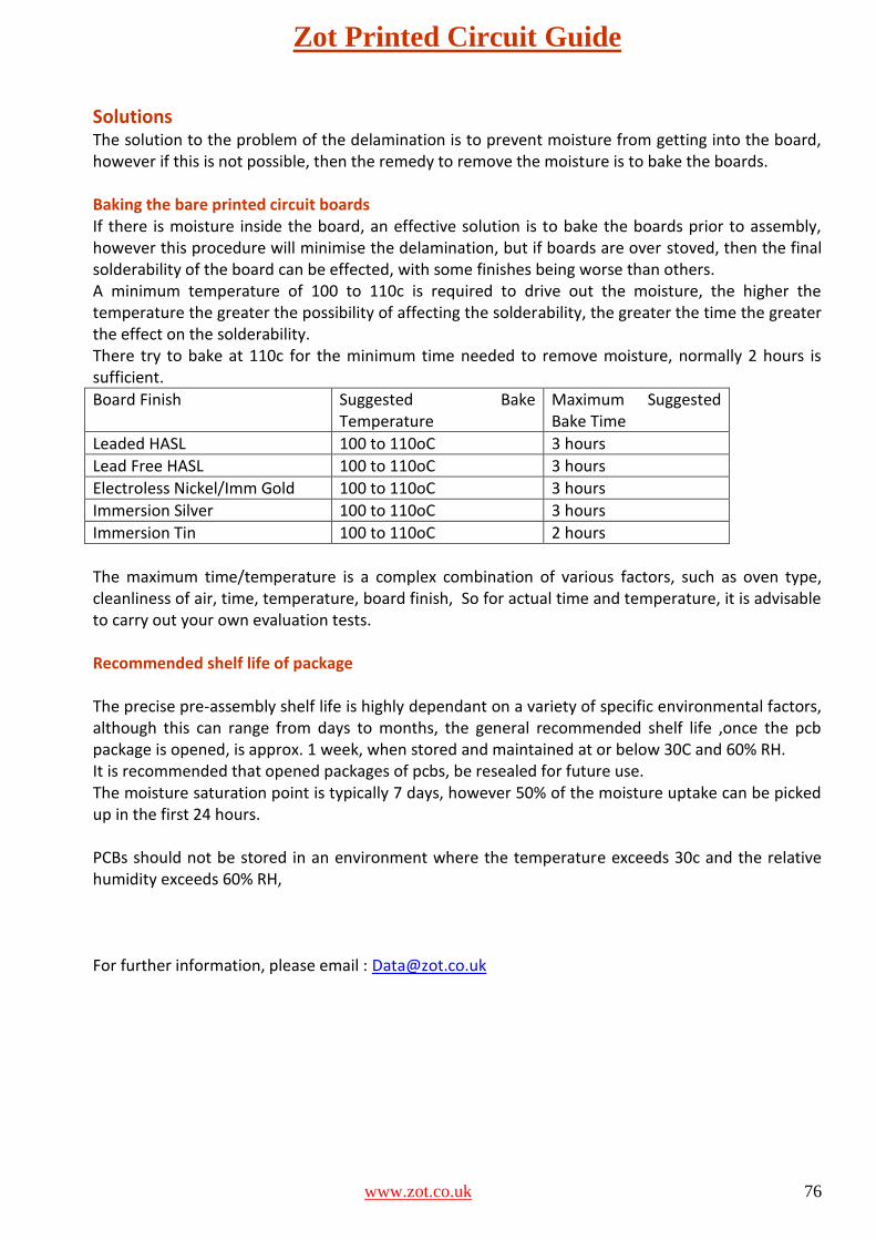
Zot Printed Circuit Guide
www.zot.co.uk 76
Solutions The solution to the problem of the delamination is to prevent moisture from getting into the board, however if this is not possible, then the remedy to remove the moisture is to bake the boards. Baking the bare printed circuit boards If there is moisture inside the board, an effective solution is to bake the boards prior to assembly, however this procedure will minimise the delamination, but if boards are over stoved, then the final solderability of the board can be effected, with some finishes being worse than others. A minimum temperature of 100 to 110c is required to drive out the moisture, the higher the temperature the greater the possibility of affecting the solderability, the greater the time the greater the effect on the solderability. There try to bake at 110c for the minimum time needed to remove moisture, normally 2 hours is sufficient.
Board Finish Suggested Bake Temperature
Maximum Suggested Bake Time
Leaded HASL 100 to 110oC 3 hours
Lead Free HASL 100 to 110oC 3 hours
Electroless Nickel/Imm Gold 100 to 110oC 3 hours
Immersion Silver 100 to 110oC 3 hours
Immersion Tin 100 to 110oC 2 hours
The maximum time/temperature is a complex combination of various factors, such as oven type, cleanliness of air, time, temperature, board finish, So for actual time and temperature, it is advisable to carry out your own evaluation tests. Recommended shelf life of package The precise pre-assembly shelf life is highly dependant on a variety of specific environmental factors, although this can range from days to months, the general recommended shelf life ,once the pcb package is opened, is approx. 1 week, when stored and maintained at or below 30C and 60% RH. It is recommended that opened packages of pcbs, be resealed for future use. The moisture saturation point is typically 7 days, however 50% of the moisture uptake can be picked up in the first 24 hours. PCBs should not be stored in an environment where the temperature exceeds 30c and the relative humidity exceeds 60% RH, For further information, please email : [email protected]
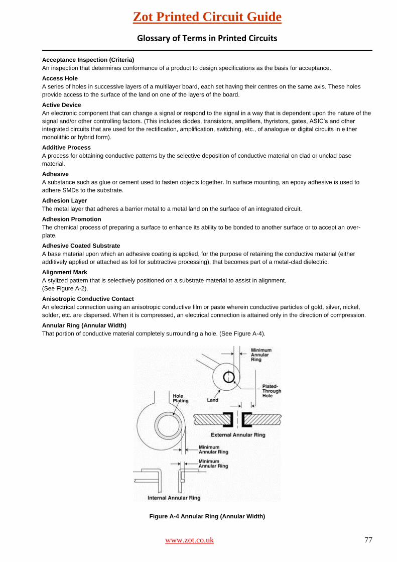
Zot Printed Circuit Guide
www.zot.co.uk 77
Glossary of Terms in Printed Circuits
Acceptance Inspection (Criteria)
An inspection that determines conformance of a product to design specifications as the basis for acceptance.
Access Hole
A series of holes in successive layers of a multilayer board, each set having their centres on the same axis. These holes
provide access to the surface of the land on one of the layers of the board.
Active Device
An electronic component that can change a signal or respond to the signal in a way that is dependent upon the nature of the
signal and/or other controlling factors. (This includes diodes, transistors, amplifiers, thyristors, gates, ASIC’s and other
integrated circuits that are used for the rectification, amplification, switching, etc., of analogue or digital circuits in either
monolithic or hybrid form).
Additive Process
A process for obtaining conductive patterns by the selective deposition of conductive material on clad or unclad base
material.
Adhesive
A substance such as glue or cement used to fasten objects together. In surface mounting, an epoxy adhesive is used to
adhere SMDs to the substrate.
Adhesion Layer
The metal layer that adheres a barrier metal to a metal land on the surface of an integrated circuit.
Adhesion Promotion
The chemical process of preparing a surface to enhance its ability to be bonded to another surface or to accept an over-
plate.
Adhesive Coated Substrate
A base material upon which an adhesive coating is applied, for the purpose of retaining the conductive material (either
additively applied or attached as foil for subtractive processing), that becomes part of a metal-clad dielectric.
Alignment Mark
A stylized pattern that is selectively positioned on a substrate material to assist in alignment.
(See Figure A-2).
Anisotropic Conductive Contact
An electrical connection using an anisotropic conductive film or paste wherein conductive particles of gold, silver, nickel,
solder, etc. are dispersed. When it is compressed, an electrical connection is attained only in the direction of compression.
Annular Ring (Annular Width)
That portion of conductive material completely surrounding a hole. (See Figure A-4).
Figure A-4 Annular Ring (Annular Width)
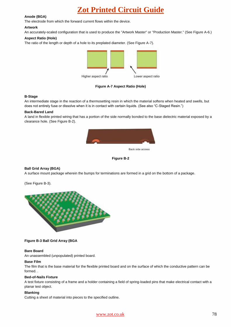
Zot Printed Circuit Guide
www.zot.co.uk 78
Anode (BGA)
The electrode from which the forward current flows within the device.
Artwork
An accurately-scaled configuration that is used to produce the "Artwork Master" or "Production Master." (See Figure A-6.)
Aspect Ratio (Hole)
The ratio of the length or depth of a hole to its preplated diameter. (See Figure A-7).
Figure A-7 Aspect Ratio (Hole)
B-Stage
An intermediate stage in the reaction of a thermosetting resin in which the material softens when heated and swells, but
does not entirely fuse or dissolve when it is in contact with certain liquids. (See also “C-Staged Resin.”)
Back-Bared Land
A land in flexible printed wiring that has a portion of the side normally bonded to the base dielectric material exposed by a
clearance hole. (See Figure B-2).
Figure B-2
Ball Grid Array (BGA)
A surface mount package wherein the bumps for terminations are formed in a grid on the bottom of a package.
(See Figure B-3).
Figure B-3 Ball Grid Array (BGA
Bare Board
An unassembled (unpopulated) printed board.
Base Film
The film that is the base material for the flexible printed board and on the surface of which the conductive pattern can be
formed. .
Bed-of-Nails Fixture
A test fixture consisting of a frame and a holder containing a field of spring-loaded pins that make electrical contact with a
planar test object.
Blanking
Cutting a sheet of material into pieces to the specified outline.
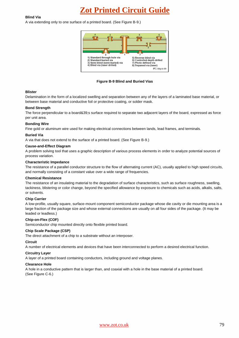
Zot Printed Circuit Guide
www.zot.co.uk 79
Blind Via
A via extending only to one surface of a printed board. (See Figure B-9.)
Figure B-9 Blind and Buried Vias
Blister
Delamination in the form of a localized swelling and separation between any of the layers of a laminated base material, or
between base material and conductive foil or protective coating, or solder mask.
Bond Strength
The force perpendicular to a board&39;s surface required to separate two adjacent layers of the board, expressed as force
per unit area.
Bonding Wire
Fine gold or aluminum wire used for making electrical connections between lands, lead frames, and terminals.
Buried Via
A via that does not extend to the surface of a printed board. (See Figure B-9.)
Cause-and-Effect Diagram
A problem solving tool that uses a graphic description of various process elements in order to analyze potential sources of
process variation.
Characteristic Impedance
The resistance of a parallel conductor structure to the flow of alternating current (AC), usually applied to high speed circuits,
and normally consisting of a constant value over a wide range of frequencies.
Chemical Resistance
The resistance of an insulating material to the degradation of surface characteristics, such as surface roughness, swelling,
tackiness, blistering or color change, beyond the specified allowance by exposure to chemicals such as acids, alkalis, salts,
or solvents.
Chip Carrier
A low-profile, usually square, surface-mount component semiconductor package whose die cavity or die mounting area is a
large fraction of the package size and whose external connections are usually on all four sides of the package. (It may be
leaded or leadless.)
Chip-on-Flex (COF)
Semiconductor chip mounted directly onto flexible printed board.
Chip Scale Package (CSP)
The direct attachment of a chip to a substrate without an interposer.
Circuit
A number of electrical elements and devices that have been interconnected to perform a desired electrical function.
Circuitry Layer
A layer of a printed board containing conductors, including ground and voltage planes.
Clearance Hole
A hole in a conductive pattern that is larger than, and coaxial with a hole in the base material of a printed board.
(See Figure C-6.)
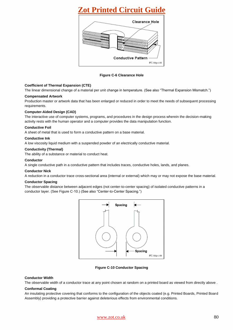
Zot Printed Circuit Guide
www.zot.co.uk 80
Figure C-6 Clearance Hole
Coefficient of Thermal Expansion (CTE)
The linear dimensional change of a material per unit change in temperature. (See also “Thermal Expansion Mismatch.”)
Compensated Artwork
Production master or artwork data that has been enlarged or reduced in order to meet the needs of subsequent processing
requirements.
Computer-Aided Design (CAD)
The interactive use of computer systems, programs, and procedures in the design process wherein the decision-making
activity rests with the human operator and a computer provides the data manipulation function.
Conductive Foil
A sheet of metal that is used to form a conductive pattern on a base material.
Conductive Ink
A low viscosity liquid medium with a suspended powder of an electrically conductive material.
Conductivity (Thermal)
The ability of a substance or material to conduct heat.
Conductor
A single conductive path in a conductive pattern that includes traces, conductive holes, lands, and planes.
Conductor Nick
A reduction in a conductor trace cross-sectional area (internal or external) which may or may not expose the base material.
Conductor Spacing
The observable distance between adjacent edges (not center-to-center spacing) of isolated conductive patterns in a
conductor layer. (See Figure C-10.) (See also “Center-to-Center Spacing.”)
Figure C-10 Conductor Spacing
Conductor Width
The observable width of a conductor trace at any point chosen at random on a printed board as viewed from directly above .
Conformal Coating
An insulating protective covering that conforms to the configuration of the objects coated (e.g. Printed Boards, Printed Board
Assembly) providing a protective barrier against deleterious effects from environmental conditions.
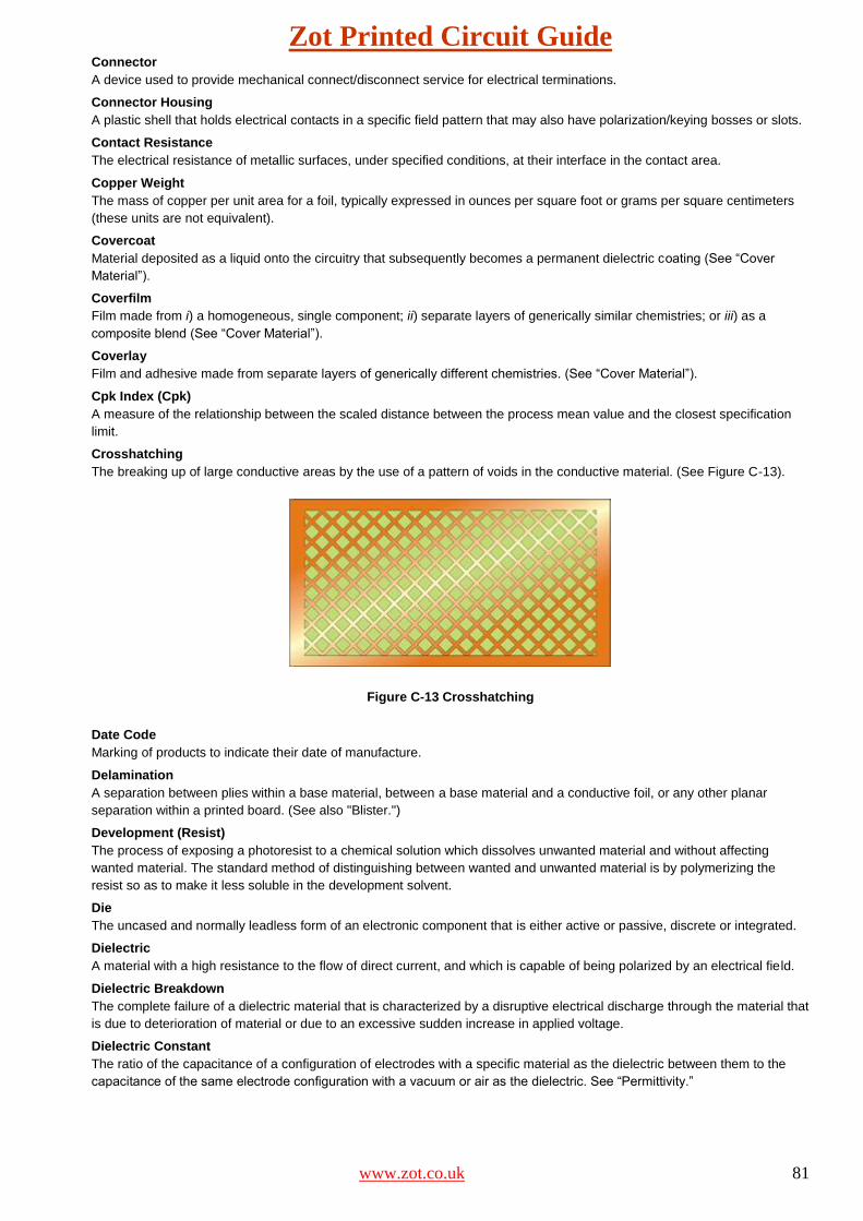
Zot Printed Circuit Guide
www.zot.co.uk 81
Connector
A device used to provide mechanical connect/disconnect service for electrical terminations.
Connector Housing
A plastic shell that holds electrical contacts in a specific field pattern that may also have polarization/keying bosses or slots.
Contact Resistance
The electrical resistance of metallic surfaces, under specified conditions, at their interface in the contact area.
Copper Weight
The mass of copper per unit area for a foil, typically expressed in ounces per square foot or grams per square centimeters
(these units are not equivalent).
Covercoat
Material deposited as a liquid onto the circuitry that subsequently becomes a permanent dielectric coating (See “Cover
Material”).
Coverfilm
Film made from i) a homogeneous, single component; ii) separate layers of generically similar chemistries; or iii) as a
composite blend (See “Cover Material”).
Coverlay
Film and adhesive made from separate layers of generically different chemistries. (See “Cover Material”).
Cpk Index (Cpk)
A measure of the relationship between the scaled distance between the process mean value and the closest specification
limit.
Crosshatching
The breaking up of large conductive areas by the use of a pattern of voids in the conductive material. (See Figure C-13).
Figure C-13 Crosshatching
Date Code
Marking of products to indicate their date of manufacture.
Delamination
A separation between plies within a base material, between a base material and a conductive foil, or any other planar
separation within a printed board. (See also "Blister.")
Development (Resist)
The process of exposing a photoresist to a chemical solution which dissolves unwanted material and without affecting
wanted material. The standard method of distinguishing between wanted and unwanted material is by polymerizing the
resist so as to make it less soluble in the development solvent.
Die
The uncased and normally leadless form of an electronic component that is either active or passive, discrete or integrated.
Dielectric
A material with a high resistance to the flow of direct current, and which is capable of being polarized by an electrical field.
Dielectric Breakdown
The complete failure of a dielectric material that is characterized by a disruptive electrical discharge through the material that
is due to deterioration of material or due to an excessive sudden increase in applied voltage.
Dielectric Constant
The ratio of the capacitance of a configuration of electrodes with a specific material as the dielectric between them to the
capacitance of the same electrode configuration with a vacuum or air as the dielectric. See “Permittivity.”
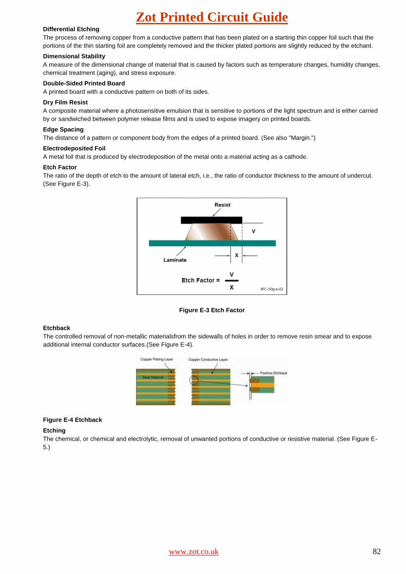
Zot Printed Circuit Guide
www.zot.co.uk 82
Differential Etching
The process of removing copper from a conductive pattern that has been plated on a starting thin copper foil such that the
portions of the thin starting foil are completely removed and the thicker plated portions are slightly reduced by the etchant.
Dimensional Stability
A measure of the dimensional change of material that is caused by factors such as temperature changes, humidity changes,
chemical treatment (aging), and stress exposure.
Double-Sided Printed Board
A printed board with a conductive pattern on both of its sides.
Dry Film Resist
A composite material where a photosensitive emulsion that is sensitive to portions of the light spectrum and is either carried
by or sandwiched between polymer release films and is used to expose imagery on printed boards.
Edge Spacing
The distance of a pattern or component body from the edges of a printed board. (See also "Margin.")
Electrodeposited Foil
A metal foil that is produced by electrodeposition of the metal onto a material acting as a cathode.
Etch Factor
The ratio of the depth of etch to the amount of lateral etch, i.e., the ratio of conductor thickness to the amount of undercut.
(See Figure E-3).
Figure E-3 Etch Factor
Etchback
The controlled removal of non-metallic materialsfrom the sidewalls of holes in order to remove resin smear and to expose
additional internal conductor surfaces.(See Figure E-4).
Figure E-4 Etchback
Etching
The chemical, or chemical and electrolytic, removal of unwanted portions of conductive or resistive material. (See Figure E-
5.)
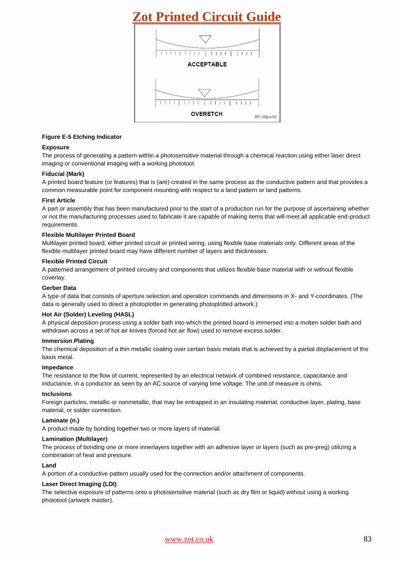
Zot Printed Circuit Guide
www.zot.co.uk 83
Figure E-5 Etching Indicator
Exposure
The process of generating a pattern within a photosensitive material through a chemical reaction using either laser direct
imaging or conventional imaging with a working phototool.
Fiducial (Mark)
A printed board feature (or features) that is (are) created in the same process as the conductive pattern and that provides a
common measurable point for component mounting with respect to a land pattern or land patterns.
First Article
A part or assembly that has been manufactured prior to the start of a production run for the purpose of ascertaining whether
or not the manufacturing processes used to fabricate it are capable of making items that will meet all applicable end-product
requirements.
Flexible Multilayer Printed Board
Multilayer printed board, either printed circuit or printed wiring, using flexible base materials only. Different areas of the
flexible multilayer printed board may have different number of layers and thicknesses.
Flexible Printed Circuit
A patterned arrangement of printed circuitry and components that utilizes flexible base material with or without flexible
coverlay.
Gerber Data
A type of data that consists of aperture selection and operation commands and dimensions in X- and Y-coordinates. (The
data is generally used to direct a photoplotter in generating photoplotted artwork.)
Hot Air (Solder) Leveling (HASL)
A physical deposition process using a solder bath into which the printed board is immersed into a molten solder bath and
withdrawn across a set of hot air knives (forced hot air flow) used to remove excess solder.
Immersion Plating
The chemical deposition of a thin metallic coating over certain basis metals that is achieved by a partial displacement of the
basis metal.
Impedance
The resistance to the flow of current, represented by an electrical network of combined resistance, capacitance and
inductance, in a conductor as seen by an AC source of varying time voltage. The unit of measure is ohms.
Inclusions
Foreign particles, metallic or nonmetallic, that may be entrapped in an insulating material, conductive layer, plating, base
material, or solder connection.
Laminate (n.)
A product made by bonding together two or more layers of material.
Lamination (Multilayer)
The process of bonding one or more innerlayers together with an adhesive layer or layers (such as pre-preg) utilizing a
combination of heat and pressure.
Land
A portion of a conductive pattern usually used for the connection and/or attachment of components.
Laser Direct Imaging (LDI)
The selective exposure of patterns onto a photosensitive material (such as dry film or liquid) without using a working
phototool (artwork master).
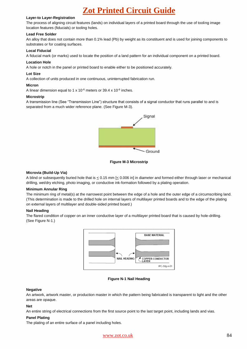
Zot Printed Circuit Guide
www.zot.co.uk 84
Layer-to Layer-Registration
The process of aligning circuit features (lands) on individual layers of a printed board through the use of tooling image
location features (fiducials) or tooling holes.
Lead Free Solder
An alloy that does not contain more than 0.1% lead (Pb) by weight as its constituent and is used for joining components to
substrates or for coating surfaces.
Local Fiducial
A fiducial mark (or marks) used to locate the position of a land pattern for an individual component on a printed board.
Location Hole
A hole or notch in the panel or printed board to enable either to be positioned accurately.
Lot Size
A collection of units produced in one continuous, uninterrupted fabrication run.
Micron
A linear dimension equal to 1 x 10⁻⁶ meters or 39.4 x 10⁻⁶ inches.
Microstrip
A transmission line (See “Transmission Line”) structure that consists of a signal conductor that runs parallel to and is
separated from a much wider reference plane. (See Figure M-3).
Figure M-3 Microstrip
Microvia (Build-Up Via)
A blind or subsequently buried hole that is < 0.15 mm [< 0.006 in] in diameter and formed either through laser or mechanical
drilling, wet/dry etching, photo imaging, or conductive ink-formation followed by a plating operation.
Minimum Annular Ring
The minimum ring of metal(s) at the narrowest point between the edge of a hole and the outer edge of a circumscribing land.
(This determination is made to the drilled hole on internal layers of multilayer printed boards and to the edge of the plating
on external layers of multilayer and double-sided printed board.)
Nail Heading
The flared condition of copper on an inner conductive layer of a multilayer printed board that is caused by hole-drilling.
(See Figure N-1.)
Figure N-1 Nail Heading
Negative
An artwork, artwork master, or production master in which the pattern being fabricated is transparent to light and the other
areas are opaque.
Net
An entire string of electrical connections from the first source point to the last target point, including lands and vias.
Panel Plating
The plating of an entire surface of a panel including holes.
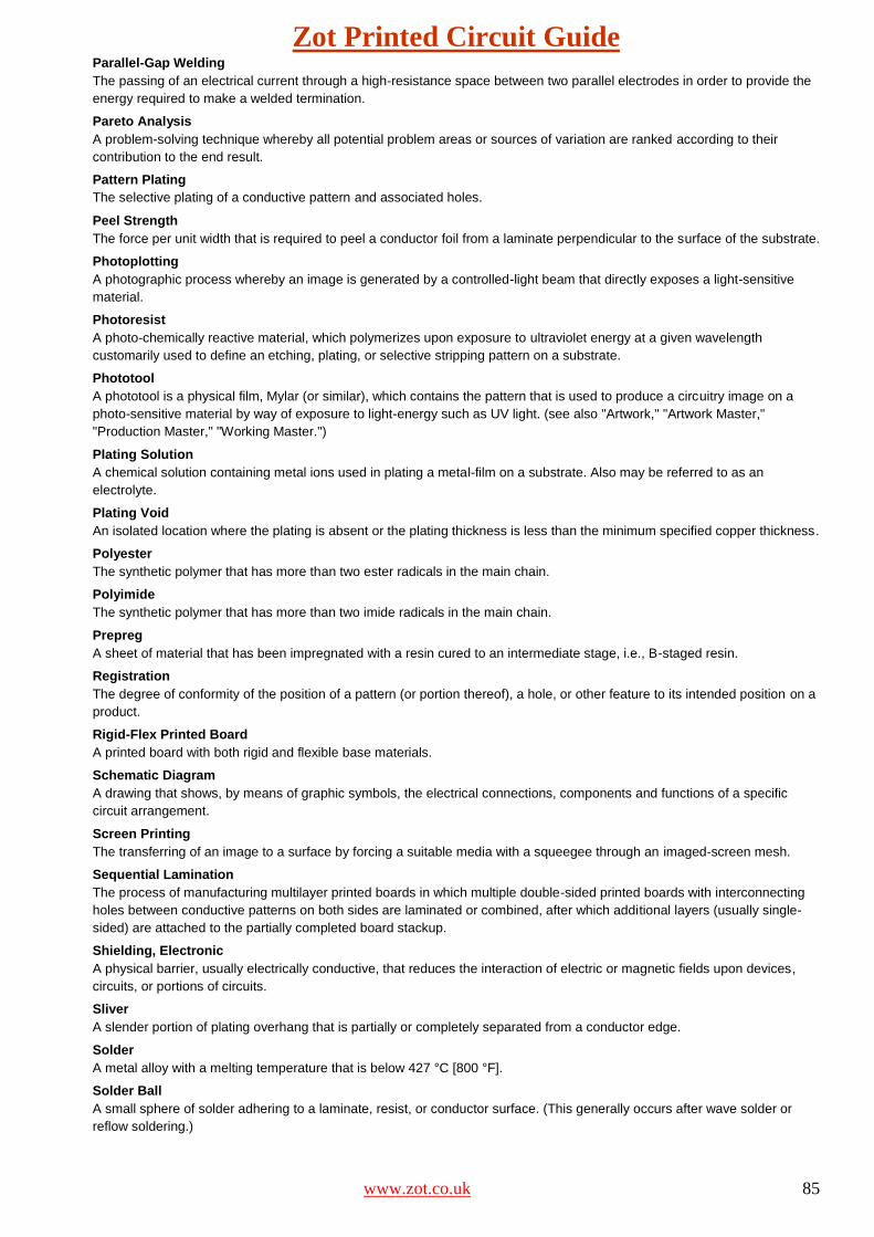
Zot Printed Circuit Guide
www.zot.co.uk 85
Parallel-Gap Welding
The passing of an electrical current through a high-resistance space between two parallel electrodes in order to provide the
energy required to make a welded termination.
Pareto Analysis
A problem-solving technique whereby all potential problem areas or sources of variation are ranked according to their
contribution to the end result.
Pattern Plating
The selective plating of a conductive pattern and associated holes.
Peel Strength
The force per unit width that is required to peel a conductor foil from a laminate perpendicular to the surface of the substrate.
Photoplotting
A photographic process whereby an image is generated by a controlled-light beam that directly exposes a light-sensitive
material.
Photoresist
A photo-chemically reactive material, which polymerizes upon exposure to ultraviolet energy at a given wavelength
customarily used to define an etching, plating, or selective stripping pattern on a substrate.
Phototool
A phototool is a physical film, Mylar (or similar), which contains the pattern that is used to produce a circuitry image on a
photo-sensitive material by way of exposure to light-energy such as UV light. (see also "Artwork," "Artwork Master,"
"Production Master," "Working Master.")
Plating Solution
A chemical solution containing metal ions used in plating a metal-film on a substrate. Also may be referred to as an
electrolyte.
Plating Void
An isolated location where the plating is absent or the plating thickness is less than the minimum specified copper thickness.
Polyester
The synthetic polymer that has more than two ester radicals in the main chain.
Polyimide
The synthetic polymer that has more than two imide radicals in the main chain.
Prepreg
A sheet of material that has been impregnated with a resin cured to an intermediate stage, i.e., B-staged resin.
Registration
The degree of conformity of the position of a pattern (or portion thereof), a hole, or other feature to its intended position on a
product.
Rigid-Flex Printed Board
A printed board with both rigid and flexible base materials.
Schematic Diagram
A drawing that shows, by means of graphic symbols, the electrical connections, components and functions of a specific
circuit arrangement.
Screen Printing
The transferring of an image to a surface by forcing a suitable media with a squeegee through an imaged-screen mesh.
Sequential Lamination
The process of manufacturing multilayer printed boards in which multiple double-sided printed boards with interconnecting
holes between conductive patterns on both sides are laminated or combined, after which additional layers (usually single-
sided) are attached to the partially completed board stackup.
Shielding, Electronic
A physical barrier, usually electrically conductive, that reduces the interaction of electric or magnetic fields upon devices,
circuits, or portions of circuits.
Sliver
A slender portion of plating overhang that is partially or completely separated from a conductor edge.
Solder
A metal alloy with a melting temperature that is below 427 °C [800 °F].
Solder Ball
A small sphere of solder adhering to a laminate, resist, or conductor surface. (This generally occurs after wave solder or
reflow soldering.)
Zot Printed Circuit Guide
www.zot.co.uk 86
Solder Fillet
Solder, with a normally concave surface, that is at the intersection of the metal surfaces of the solder connection.
Solder Mask .
A heat-resisting coating material applied to selected areas to prevent the deposition of solder upon those areas during
subsequent soldering.
Squeegee
A metal or rubber blade used to wipe a material (ink or solder paste) across a stencil or silk screen to force the material
through the openings in the screen or stencil, onto the surface of a printed board or mounting structure.
Stacked Via/Microvia
A via/microvia structure formed by stacking one or more build-up vias/microvias in a build-up multilayer providing an
interlayer connection between three or more conductive layers.
Staking, Mechanical
The attaching of metallic devices, such as solder terminals and eyelets, by the upsetting of the portion of the device that
protrudes through a hole in a base material.
Stencil (Solder Paste/Adhesive)
A thin sheet of material containing openings to reflect a specific pattern, designed to transfer a paste-like material to a
substrate for the purpose of component attachment.
Step-and-Repeat
A method of dimensionally positioning multiples of the same or intermixed functional patterns accurately within a given area
on the phototool or by repetitious contact, projection printing or photoplotting.
Stiffener Board
A material fastened to the surface of a flexible circuit to increase its mechanical strength.
Strip (Resist Stripping)
The process of removing unneeded masking material, such as a photoresist or metallic etch resist, after a processing step is
completed.
Stripline
A transmission line structure that consists of a signal line that runs parallel to and is sandwiched between and separated by
a dielectric from two reference planes.
Thermoset
A plastic that undergoes a chemical reaction when exposed to elevated temperatures that leads to it having a relatively
infusible or crosslinked stated that cannot be softened or reshaped by subsequent heating.
Tinning
The application of molten solder to a basis metal in order to increase its solderability.
Ultrasonic Bond
A bond formed when a wire is pressed against the bonding pad and the pressing mechanism is ultrasonically vibrated at
high frequency (above 10kHz).
Via
A plated-through hole that is used as an interlayer connection, but in which there is no intention to insert a component lead
or other reinforcing material. (See also "Blind Via" and "Buried Via.")
Wetting
The spreading of molten solder or glass on a metallic or nonmetallic surface, with proper application of heat and in some
cases flux.
Whisker
A slender, acicular metallic growth filament that is between a conductor and a land.
Wicking
The capillary absorption of a liquid along the fibers of a base material. (See also "Solder Wicking")
Zot Printed Circuit Guide
www.zot.co.uk 87
Printed Circuit Division - Contact Details
Sales Area Representatives
North England - Business Development / Sales Name: E-Mail: [email protected] Mobile: 07725 226515
Southern England / UK Sales Manager Name: Daniel Priest UK Sales Manager E-Mail: [email protected] Mobile: 07725 226515
Scotland - Sales Engineer Name: Bill Bachop E-Mail: [email protected] Tel: 0131 653 4618 (Direct Line) Fax: 0131 653 6025 Mob: 07725226577
International Sales
Internal PCB Sales Contact
PCB Internal Sales/ Global Procurement Name: Bill Bachop E-Mail: [email protected] Tel: 0131 653 4618 (Direct Line) Fax: 0131 653 6025 Mob: 07725226577
PCB Internal Sales Name: Bill Bachop E-Mail: [email protected] Tel: 0131 653 4618 (Direct Line) Fax: 0131 653 6025 Mob: 07725226577
PCB Division Key Personnel
General Manager Name: Gordon Falconer E-Mail: [email protected] Tel: 0131 653 4626 (Direct Line) Fax: 0131 653 6025 Mob: 07725226585
PCB Quality Manager Name: Neil Richardson E-Mail: [email protected] Tel: 0131 653 4622 (Direct Line) Fax: 0131 653 6025 Mob:
Technical Manager Name: Gary Kerr E-Mail: [email protected] Tel: 0131 653 6834 (Direct Line) Fax: 0131 653 6025 Mob: 07725226581
Front End Engineering & Test Manager Name: Robert Brown E-Mail: [email protected] Tel: 0131 653 4616 (Direct Line) Fax: 0131 653 6025 Mob:
Website: www.zot.co.uk
Zot Engineering Ltd, Inveresk Industrial Park, Musselburgh, EH21 7UQ,
East Lothian, Scotland, Tel: 0131 653 6834, Fax: 0131 653 6025
Email: [email protected]


