ZM2ö Ã-ÁýðÉò±$ ¡½d5$ Ë'jÚ ';ÉX :P** þ4B < êì · Title: ZM2ö Ã-ÁýðÉò±$...
15
To learn more about ON Semiconductor, please visit our website at www.onsemi.com Please note: As part of the Fairchild Semiconductor integration, some of the Fairchild orderable part numbers will need to change in order to meet ON Semiconductor’s system requirements. Since the ON Semiconductor product management systems do not have the ability to manage part nomenclature that utilizes an underscore (_), the underscore (_) in the Fairchild part numbers will be changed to a dash (-). This document may contain device numbers with an underscore (_). Please check the ON Semiconductor website to verify the updated device numbers. The most current and up-to-date ordering information can be found at www.onsemi.com. Please email any questions regarding the system integration to [email protected]. Is Now Part of ON Semiconductor and the ON Semiconductor logo are trademarks of Semiconductor Components Industries, LLC dba ON Semiconductor or its subsidiaries in the United States and/or other countries. ON Semiconductor owns the rights to a number of patents, trademarks, copyrights, trade secrets, and other intellectual property. A listing of ON Semiconductor’s product/patent coverage may be accessed at www.onsemi.com/site/pdf/Patent-Marking.pdf. ON Semiconductor reserves the right to make changes without further notice to any products herein. ON Semiconductor makes no warranty, representation or guarantee regarding the suitability of its products for any particular purpose, nor does ON Semiconductor assume any liability arising out of the application or use of any product or circuit, and specifically disclaims any and all liability, including without limitation special, consequential or incidental damages. Buyer is responsible for its products and applications using ON Semiconductor products, including compliance with all laws, regulations and safety requirements or standards, regardless of any support or applications information provided by ON Semiconductor. “Typical” parameters which may be provided in ON Semiconductor data sheets and/or specifications can and do vary in different applications and actual performance may vary over time. All operating parameters, including “Typicals” must be validated for each customer application by customer’s technical experts. ON Semiconductor does not convey any license under its patent rights nor the rights of others. ON Semiconductor products are not designed, intended, or authorized for use as a critical component in life support systems or any FDA Class 3 medical devices or medical devices with a same or similar classification in a foreign jurisdiction or any devices intended for implantation in the human body. Should Buyer purchase or use ON Semiconductor products for any such unintended or unauthorized application, Buyer shall indemnify and hold ON Semiconductor and its officers, employees, subsidiaries, affiliates, and distributors harmless against all claims, costs, damages, and expenses, and reasonable attorney fees arising out of, directly or indirectly, any claim of personal injury or death associated with such unintended or unauthorized use, even if such claim alleges that ON Semiconductor was negligent regarding the design or manufacture of the part. ON Semiconductor is an Equal Opportunity/Affirmative Action Employer. This literature is subject to all applicable copyright laws and is not for resale in any manner.
Transcript of ZM2ö Ã-ÁýðÉò±$ ¡½d5$ Ë'jÚ ';ÉX :P** þ4B < êì · Title: ZM2ö Ã-ÁýðÉò±$...

To learn more about ON Semiconductor, please visit our website at www.onsemi.com
Please note: As part of the Fairchild Semiconductor integration, some of the Fairchild orderable part numbers will need to change in order to meet ON Semiconductor’s system requirements. Since the ON Semiconductor product management systems do not have the ability to manage part nomenclature that utilizes an underscore (_), the underscore (_) in the Fairchild part numbers will be changed to a dash (-). This document may contain device numbers with an underscore (_). Please check the ON Semiconductor website to verify the updated device numbers. The most current and up-to-date ordering information can be found at www.onsemi.com. Please email any questions regarding the system integration to [email protected].
Is Now Part of
ON Semiconductor and the ON Semiconductor logo are trademarks of Semiconductor Components Industries, LLC dba ON Semiconductor or its subsidiaries in the United States and/or other countries. ON Semiconductor owns the rights to a number of patents, trademarks, copyrights, trade secrets, and other intellectual property. A listing of ON Semiconductor’s product/patent coverage may be accessed at www.onsemi.com/site/pdf/Patent-Marking.pdf. ON Semiconductor reserves the right to make changes without further notice to any products herein. ON Semiconductor makes no warranty, representation or guarantee regarding the suitability of its products for any particular purpose, nor does ON Semiconductor assume any liability arising out of the application or use of any product or circuit, and specifically disclaims any and all liability, including without limitation special, consequential or incidental damages. Buyer is responsible for its products and applications using ON Semiconductor products, including compliance with all laws, regulations and safety requirements or standards, regardless of any support or applications information provided by ON Semiconductor. “Typical” parameters which may be provided in ON Semiconductor data sheets and/or specifications can and do vary in different applications and actual performance may vary over time. All operating parameters, including “Typicals” must be validated for each customer application by customer’s technical experts. ON Semiconductor does not convey any license under its patent rights nor the rights of others. ON Semiconductor products are not designed, intended, or authorized for use as a critical component in life support systems or any FDA Class 3 medical devices or medical devices with a same or similar classification in a foreign jurisdiction or any devices intended for implantation in the human body. Should Buyer purchase or use ON Semiconductor products for any such unintended or unauthorized application, Buyer shall indemnify and hold ON Semiconductor and its officers, employees, subsidiaries, affiliates, and distributors harmless against all claims, costs, damages, and expenses, and reasonable attorney fees arising out of, directly or indirectly, any claim of personal injury or death associated with such unintended or unauthorized use, even if such claim alleges that ON Semiconductor was negligent regarding the design or manufacture of the part. ON Semiconductor is an Equal Opportunity/Affirmative Action Employer. This literature is subject to all applicable copyright laws and is not for resale in any manner.

tm
©2008 Fairchild Semiconductor Corporation 1 www.fairchildsemi.com
February 2009
FPF2223-FPF2225 Rev. C
FPF2223-FP
F2225 Integrated Load Sw
itch with A
djustable High P
recision Current Lim
it
FPF2223-FPF2225Integrated Load Switch with Adjustable High Precision Current Limit
Features � 1.8 to 5.5V Input Voltage Range� Typical RDS(ON) = 140m� @ VIN = 5.5V� Typical RDS(ON) = 160m� @ VIN = 3.3V� 250-625mA (min) Adjustable Current Limit� 5% Current Limit Tolerance @ 625mA (min)� 72� (typ) Output Discharge Resistance� ESD Protected, Above 8kV HBM and 2kV CDM
Applications � PDAs� Cell Phones� GPS Devices� MP3 Players� Digital Cameras� Peripheral Ports� Notebook Computer
General DescriptionThe FPF2223-FPF2225 are low RDS(ON) P-Channel MOSFETload switches with high precision current limit value. The inputvoltage range operates from 1.8V to 5.5V to fulfill today's UltraPortable Device's supply requirement. Switch control is by alogic input (ON) capable of interfacing directly with low voltagecontrol signal. On-chip pull-down is available for output quickdischarge when switch is turned off.
For the FPF2224, if the constant current condition still persistsafter 30ms, these parts will shut off the switch and pull the faultsignal pin (FLAGB) low. The FPF2223 has an auto-restartfeature, which will turn the switch on again after 450mS if theON pin is still active. The FPF2224 do not have this auto-restartfeature so the switch will remain off until the ON pin is cycled.For the FPF2225, a current limit condition will immediately pullthe fault signal pin low and the part will remain in the constant-current mode until the switch current falls below the currentlimit. For the FPF2223 through FPF2225, the current limit is setby an external resistor and the minimum current limit is 250mA.
Ordering Information
Part Current Limit (mA)
Current Limit Blanking Time
(mS)
Auto-Restart Time (mS)
ON PinActivity
FPF2223 250-625 30 450 Active HI
FPF2224 250-625 30 NA Active HI
FPF2225 250-625 NA NA Active HI
BOTTOM TOP
Pin 1
mdaniels
New Logo

2 www.fairchildsemi.comFPF2223-FPF2225 Rev. C
FPF2223-FP
F2225 Integrated Load Sw
itch with A
djustable High P
recision Current Lim
it
Typical Application Circuit
Functional Block Diagram
OFF ON ON
VIN
GND
FPF2223/4/5
ISET
VOUT
TO LOAD
FLAGB
UVLO
THERMAL SHUTDOWN
CURRENT LIMIT
CONTROL LOGIC
VIN
ON
ISET
FLAGB
GND
VOUT
Output Discharge

3 www.fairchildsemi.comFPF2223-FPF2225 Rev. C
FPF2223-FP
F2225 Integrated Load Sw
itch with A
djustable High P
recision Current Lim
it
Pin Configuration
Pin Description
Absolute Maximum Ratings
Recommended Operating Range
Electrical Characteristics VIN = 1.8 to 5.5V, TA = -40 to +85°C unless otherwise noted. Typical values are at VIN = 3.3V and TA = 25°C.
Pin Name Function1 ISET Current Limit Set Input : A resistor from ISET to ground sets the current limit for the switch
2 VIN Supply Input: Input to the power switch and the supply voltage for the IC
3 VOUT Switch Output: Output of the power switch
4 FLAGBFault Output: Active LO, open drain output which indicates an over current, supply under voltage or over temperature state
5 GND Ground
6 ON ON/OFF Control Input
Parameter Min. Max. UnitVIN, VOUT, ON, FLAGB TO GND -0.3 6 V
ISET TO GND -0.3 0.3 V
Power Dissipation @ TA = 25°C 1.2 W
Operating and Storage Junction Temperature -65 125 °C
Thermal Resistance, Junction to Ambient 86 °C/W
Electrostatic Discharge Protection HBM 8000 V
MM 400 V
CDM 2000 V
Parameter Min. Max. UnitVIN 1.8 5.5 V
Ambient Operating Temperature, TA -40 85 °C
Parameter Symbol Conditions Min. Typ. Max. UnitsBasic Operation
Operating Voltage VIN 1.8 5.5 V
Quiescent Current IQ
IOUT=0mA, VIN=VON=1.8V, RSET=36K 45 75
�AIOUT=0mA, VIN=VON=3.3V, RSET=36K 50 80
IOUT=0mA, VIN=VON=5.5V, RSET=36K 55 95
VIN Shutdown Current VON=0V, VIN=5.5V, VOUT=short to GND 2.5 �A
FLAGB
GND
ISET1
2
3
6
5
4
VIN
VOUT
ON
MicroFET 2x2 6L(BOTTOMVIEW)

4 www.fairchildsemi.comFPF2223-FPF2225 Rev. C
FPF2223-FP
F2225 Integrated Load Sw
itch with A
djustable High P
recision Current Lim
it
VOUT Shutdown Current VON=0V, VOUT=5.5V, VIN=short to GND 1 �A
On-Resistance RON
VIN=5.5V, IOUT=200mA, TA=25°C 140 185
m�VIN=3.3V, IOUT=200mA, TA=25°C 160 210
VIN=1.8V, IOUT=200mA, TA=25°C 230 300
VIN=3.3V, IOUT=200mA, TA=-40 to +80°C 90 265
Output Discharge Resistance VIN=3.3V, VON=0V, IOUT=10mA 72 105 �
ON Input Logic High Voltage (ON) VIHVIN=1.8V 0.8
VVIN=5.5V 1.4
ON Input Logic Low Voltage (OFF) VILVIN=1.8V 0.5
VVIN=5.5V 1.0
On Input Leakage VON = VIN or GND -1 1 �A
FLAGB Output Logic Low VoltageVIN=5.5V, ISINK=100�A 0.05 0.1
VVIN=1.8V, ISINK=100�A 0.12 0.25
FLAGB Output High LeakageCurrent
VIN=5.5V, Switch on 1 uA
Protections
Current Limit ILIMVIN=3.3V, VOUT = 3.0V, RSET=36K, TA=25°C
627 660 693 mA
Thermal Shutdown
Shutdown Threshold 140
°CReturn from Shutdown 130
Hysteresis 10
Under Voltage Shutdown UVLO VIN increasing 1.55 1.65 1.75 V
Under Voltage Shutdown Hysteresis 50 mV
Dynamic
Turn On Time tON RL=500�, CL=0.001uF 70 �S
Turn Off Time tOFF RL=500�, CL=0.001uF 600 nS
VOUT Rise Time tRISE RL=500�, CL=0.001uF 40 �S
VOUT Fall Time tFALL RL=500�, CL=0.001uF 100 nS
Over Current Blanking Time tBLANK FPF2223, FPF2224 15 30 60 mS
Auto-Restart Time tRSTRT FPF2223 225 450 900 mS
Current Limit Response TimeVIN = VON = 3.3V. Over-Current Condition: RLOAD=VIN/(ILIMx4)
5 �S
Parameter Symbol Conditions Min. Typ. Max. Units

5 www.fairchildsemi.comFPF2223-FPF2225 Rev. C
FPF2223-FP
F2225 Integrated Load Sw
itch with A
djustable High P
recision Current Lim
it
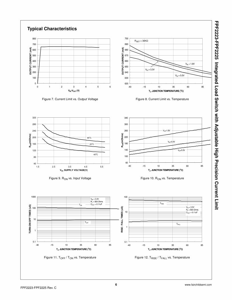
Typical Characteristics
Figure 1. Quiescent Current vs. Input Voltage Figure 2. Quiescent Current vs. Temperature
Figure 4. VON High Voltage vs. Temperature
Figure 5. VON Low Voltage vs. Temperature Figure 6. On Pin Current vs. Temperature
Figure 3. VON vs. Input Voltage
0.2
0.4
0.6
0.8
1.0
1.2
1.4
1 2 3 4 5 6
VIN, SUPPLY VOLTAGE (V)
VO
N S
UP
PLY
VO
LTA
GE
(V)
VIH
VIL
20
30
40
50
60
70
80
90
-40 -15 10 35 60 85
TJ, JUNCTION TEMPERATURE (oC)
SU
PP
LY C
UR
RE
NT
(uA
)
VIN=1.8V
VIN=3.3V
VIN=5.5V
VON=VIN
0.2
0.4
0.6
0.8
1
1.2
1.4
1.6
-40 -15 10 35 60 85
TJ, JUNCTION TEMPERATURE (oC)
VO
N S
UP
PLY
VO
LTA
GE
(V)
VIN=1.2V
VIN=3.3V
VIN=5.5V
0.0
0.2
0.4
0.6
0.8
1.0
1.2
1.4
-40 -15 10 35 60 85
TJ, JUNCTION TEMPERATURE (oC)
VO
N S
UP
PLY
VO
LTA
GE
(V)
VIN=1.2V
VIN=3.3V
VIN=5.5V
-0.01
0.00
0.01
0.02
0.03
0.04
0.05
-40 -15 10 35 60 85
TJ, JUNCTION TEMPERATURE (oC)
ON
PIN
CU
RR
EN
T (u
A)
VON = 5.5V
VON = 0V
10
20
30
40
50
60
70
80
1 2 3 4 5 6
SUPPLY VOLTAGE (V)
SU
PP
LY C
UR
RE
NT
(uA
)
25oC
-40oC
85oC
VON = VIN
6 www.fairchildsemi.comFPF2223-FPF2225 Rev. C
FPF2223-FP
F2225 Integrated Load Sw
itch with A
djustable High P
recision Current Lim
it
Typical Characteristics
Figure 7. Current Limit vs. Output Voltage Figure 8. Current Limit vs. Temperature
Figure 10. RON vs. Temperature
Figure 11. TOFF / TON vs. Temperature Figure 12. TRISE / TFALL vs. Temperature
Figure 9. RON vs. Input Voltage
40
80
120
160
200
240
280
320
1.5 2.5 3.5 4.5 5.5
VIN, SUPPLY VOLTAGE(V)
RO
N(m
Ohm
s)
85oC
25oC
-40oC
0
100
200
300
400
500
600
700
800
0 1 2 3 4 5 6
VIN-VOUT (V)
OU
TPU
T C
UR
RE
NT
(mA
)
620
630
640
650
660
670
680
690
700
-40 -15 10 35 60 85
TJ, JUNCTION TEMPERATURE (oC)
OU
TPU
T C
UR
RE
NT
(mA
)
VIN = 5.5V
VIN = 3.3V
VIN = 1.8V
60
100
140
180
220
260
300
340
-40 -15 10 35 60 85
TJ, JUNCTION TEMPERATURE (oC)
RO
N(m
Ohm
s)
VIN=1.8V
VIN=3.3V
VIN=5.5V
0.1
1
10
100
-40 -15 10 35 60 85
TJ, JUNCTION TEMPERATURE (oC)
RIS
E /
FALL
TIM
ES
(uS
)
TRISE
TFALL
VIN = 3.3VRL = 500 OhmsCOUT = 0.11uF
0.1
1
10
100
1000
-40 -15 10 35 60 85
TJ, JUNCTION TEMPERATURE (oC)
TUR
N-O
N/O
FF T
IME
S (u
S)
VIN = 3.3VRL = 500 OhmsCOUT = 0.11uF
TOFF
TON
RSET = 36K�

7 www.fairchildsemi.comFPF2223-FPF2225 Rev. C
FPF2223-FP
F2225 Integrated Load Sw
itch with A
djustable High P
recision Current Lim
it
Typical Characteristics
Figure 13. TBLANK vs Temperature Figure 14. Turn On Response
Figure 16. TBLANK Response
Figure 17. TRESTART Response Figure 18. Current Limit Response(Output is loaded with 1.2� resistor and COUT=10�F)
Figure 15. Turn Off Response
500ns/DIV
VDRV1
5V/DIV
VFLAGB2V/DIV
10ms/DIV
IOUT 500mA/DIV
VIN2V/DIV
VON2V/DIV
VOUT2V/DIV
100�s/DIV
IOUT 10mA/DIV
VIN=3.3V, RL=500�,CIN=10uF,RSET=36K�
100�s/DIV
VIN2V/DIV
VON2V/DIV
VOUT2V/DIV
IOUT 10mA/DIV
VIN=3.3V, RL=500�,CIN=10uF,RSET=36K�
VOUT2V/DIV
VIN=5V, CIN=10uF, RL=100�,COUT=1uF,RSET=36K�
TBLANK
VDRV1
5V/DIV
VFLAGB2V/DIV
100ms/DIV
IOUT 500mA/DIV
VOUT2V/DIV
VIN=5V, CIN=10uF, RL=100�,COUT=1uF,RSET=36K�
TRESTART
Note1: VDRV signal drives the gate of a NMOS transistor. The NMOS transistor is in series with a 5� resistor and is connected to theoutput of device. By turning on the transistor, the 5� resistor is loaded to the output and forces the device to go into overcurrentcondition.
VON2V/DIV
VIN2V/DIV
VOUT2V/DIV
IOUT 10mA/DIV
VIN=3.3V, CIN=10uF, RL=1.2�,COUT=10uF,RSET=36K�
1
10
100
1000
-40 -15 10 35 60 85
TJ, JUNCTION TEMPERATURE (oC)
T BLA
NK /
T RE
STA
RT
(mS
)
TRESTART
TBLANK

8 www.fairchildsemi.comFPF2223-FPF2225 Rev. C
FPF2223-FP
F2225 Integrated Load Sw
itch with A
djustable High P
recision Current Lim
it
Typical Characteristics
Figure 19. Current Limit Response(Output is loaded with 1.2� resistor and COUT=100�F)
Figure 20. Current Limit and Output Discharge Response(Device turns on and off into large capacitive load COUT=100F)
Figure 22. Short Circuit Response Time(Output shorted to GND while the switch is in normal operation)
Figure 21. Current Limit Response (Switch is powered into a short - Input and
enable pin are tied together)
50�s/DIV 20�s/DIV
500�s/DIV
VON2V/DIV
VIN5V/DIV
VOUT2V/DIV
IOUT 500mA/DIV
VIN=5V, CIN=10uF, COUT=100uF,RL=1.2�,RSET=36K�
2ms/DIV
VON2V/DIV
VIN5V/DIV
VOUT5V/DIV
IOUT 500mA/DIV
VIN=5V, CIN=10uF, RL=1.2�, COUT=100uF,RSET=36K�
VIN=VON2V/DIV
VOUT2V/DIV
IOUT 500mA/DIV
VIN=VON=3.3V, CIN=10uF, RL=1.2�, COUT=1uF,RSET=36K�
VON2V/DIV
VOUT2V/DIV
IOUT 5A/DIV
VIN=3.3V, CIN=10uF, RL=100�,COUT=1uF,RSET=36K�

9 www.fairchildsemi.comFPF2223-FPF2225 Rev. C
FPF2223-FP
F2225 Integrated Load Sw
itch with A
djustable High P
recision Current Lim
it
Description of OperationThe FPF2223, FPF2224, and FPF2225 are state of the artAdjustable High Precision Current Limit switches that protectsystems and loads which can be damaged or disrupted by theapplication of high currents. The core of each device is a 0.16�P-channel MOSFET and a controller capable of functioning overan input operating range of 1.8- 5.5V. The controller protects oroffers current limiting, UVLO(undervoltage lockout) and thermalshutdown protection. The current limit is adjustable from 250mAto 625mA through the selection of an external resistor.
On/Off ControlThe ON pin is active high, and controls the state of the switch.Applying a continuous high signal will hold the switch in the onstate. The switch will move into the OFF state when the activehigh is removed, or if a fault is encountered. For all versions, anundervoltage on VIN or a junction temperature in excess of140°C overrides the ON control to turn off the switch.In addition, excessive currents will cause the switch to turn off inthe FPF2223 and FPF2224. The FPF2223 has an Auto-Restartfeature which will automatically turn the switch on again after450ms. For the FPF2224, the ON pin must be toggled to turn-onthe switch again. The FPF2225 does not turn off in response toan over current condition but instead remains operating in aconstant current mode so long as ON is active and the thermalshutdown or UVLO have not activated.
Fault ReportingUpon the detection of an over-current condition, an input UVLO,or an over-temperature condition, the FLAGB signals the faultmode by activating LO. In the event of an over-current conditionfor the FPF2223 and FPF2224, the FLAGB goes LO at the endof the blanking time while FLAGB goes LO immediately for theFPF2225. If the over-current condition lasts longer thanblanking time, FLAGB remains LO through the Auto-RestartTime for the FPF2223 while for the FPF2224, FLAGB is latchedLO and ON must be toggled to release it. With the FPF2225,FLAGB is LO during the faults and immediately returns HI at theend of the fault condition. FLAGB is an open-drain MOSFETwhich requires a pull-up resistor between VIN and FLAGB.During shutdown, the pull-down on FLAGB is disabled to reducecurrent draw from the supply. A 100K� pull up resistor isrecommended to be used in the application.
Current LimitingThe current limit ensures that the current through the switchdoesn't exceed a maximum value while not limiting at less thana minimum value. The current at which the parts will limit isadjustable through the selection of an external resistorconnected to the ISET pin. The FPF2223 and FPF2224 have ablanking time of 30ms (nominal) during which the switch will actas a constant current source. At the end of the blanking time,the switch will be turned-off. The FPF2225 has no current limitblanking period so it will remain in a constant current state untilthe ON pin is deactivated or the thermal shutdown turns-off theswitch.
Undervoltage Lockout (UVLO)The undervoltage lockout turns-off the switch if the input voltagedrops below the undervoltage lockout threshold. With the ONpin active the input voltage rising above the undervoltagelockout threshold will cause a controlled turn-on of the switchwhich limits current over-shoots.
Output Discharge ResistorThe FPF2223/4/5 family contains an 80� on-chip load resistorfor quick output discharge when the switch is turned off. Thisfeatures become more attractive when application requireslarge output capacitor to be discharge when the switch tunrs off.However, VOUT pin should not be connected directly to thebattery source due to the discharge mechanism of the loadswitch.
Thermal ShutdownThe thermal shutdown protects the die from internally orexternally generated excessive temperatures. During an over-temperature condition the FLAGB is activated and the switch isturned-off. The switch automatically turns-on again iftemperature of the die drops below the threshold temperature.

10 www.fairchildsemi.comFPF2223-FPF2225 Rev. C
FPF2223-FP
F2225 Integrated Load Sw
itch with A
djustable High P
recision Current Lim
it
Application Information
Setting Current LimitThe FPF2223, FPF2224, and FPF2225 have adjustable highprecision current limit which is set with an external resistorconnected between ISET and GND. Please see the layoutrecommendation section of the application note for therecommended RSET layout. The RSET resistance is selected byusing the following equation:
For a particular ILIM(min) value, RSET can be calculated frombelow formula:
FPF222X family has 5% precision at higher load current. TheILIM (Max) and tolerance of current limit value can be determinedusing Figure 23 (ILIM vs RSET ) and the following formula:
The table and figure below can be used to select RSET:
Input CapacitorTo limit the voltage drop on the input supply caused by transientin-rush currents when the switch is turned on into a dischargedload capacitor or a short-circuit, a capacitor is recommended tobe placed between VIN and GND. A 1uF ceramic capacitor, CIN,placed close to the pins is usually sufficient. Higher values ofCIN can be used to further reduce the voltage drop.
Output CapacitorA 0.1uF capacitor COUT, should be placed between VOUT andGND. This capacitor will prevent parasitic board inductancesfrom forcing VOUT below GND when the switch turns-off. For theFPF2223 and FPF2224, the total output capacitance needs tobe kept below a maximum value, COUT(max), to prevent thepart from registering an over-current condition and turning-offthe switch. The maximum output capacitance can bedetermined from the following formula:
Power DissipationDuring normal on-state operation, the power dissipated in thedevice will depend upon the level at which the current limit isset. The maximum allowed setting for the current limit is 625mAand will result in a power dissipation of:
If the part goes into current limit, maximum power dissipationwill occur when the output is shorted to ground. For theFPF2223, the power dissipation will be scaled by the Auto-Restart Time, tRSTRT, and the Over Current Blanking Time,tBLANK. Therefore, the maximum power dissipated is:
RSET [k�]
Min. Current Limit [mA]
Typ. Current Limit [mA]
Max. Current Limit [mA]
Tol[%]
36.0 627.0 660.0 693.0 5.0
37.5 600.9 633.7 666.5 5.2
39.0 576.2 609.3 642.5 5.4
40.2 557.7 591.1 624.5 5.7
42.2 529.3 563.1 597.0 6.0
44.2 503.3 537.6 572.0 6.4
49.0 449.5 485.0 520.4 7.3
51.1 429.1 465.0 501.0 7.7
54.9 396.0 432.9 469.7 8.5
61.9 345.3 383.9 422.5 10.1
69.8 299.8 340.5 381.1 11.9
80.9 250.0 293.7 337.5 14.9
ILIM (Typ) (mA) =23764
RSET (K�)
RSET (K�) = 23764
ILIM (Min) (mA) + 25 +4700
ILIM (Min) (mA)
Tolerance (%) = 100 *ILIM (Typ) - ILIM (Min)
ILIM (Typ)
ILIM (Max) = ILIM (Typ) +ILIM (Typ) * Tolerance (%)
100
Table 1: RSET Selection Guide
240
300
360
420
480
540
600
660
720
34 42 50 58 66 74 82RSET (KOhms)
I LIM
IT (m
A)
Max
Min
Typ
Figure 23. ILIM vs RSET
P = (ILIM)2 * RDS = (0.625)2 * 0.165 = 64mW
P (Max) =tBLANK
tBLANK + tRSTRT* VIN (Max) * ILIM (Max)
30
30 + 450* 5.5 * 0.693 = 0.238W=
COUT (Max) =ILIM (Max) * tBLANK (Min)
VIN

11 www.fairchildsemi.comFPF2223-FPF2225 Rev. C
FPF2223-FP
F2225 Integrated Load Sw
itch with A
djustable High P
recision Current Lim
it
Take note that this is below the maximum package powerdissipation, and the thermal shutdown feature will act asadditional safety to protect the part from damage due toexcessive heating. The junction temperature is only able toincrease to the thermal shutdown threshold. Once thistemperature has been reached, toggling ON will not turn-on theswitch until the junction temperature drops. For the FPF2225, ashort on the output will cause the part to operate in a constantcurrent state dissipating a worst case power of:
This large amount of power will activate the thermal shutdownand the part will cycle in and out of thermal shutdown so long asthe ON pin is active and the short is present.
PCB Layout RecommendationsIn order to benefit from adjustable, high-precision load switchdevices, a high-precision RSET value must be used to set a tightcurrent limit tolerance. Since ILIMIT (current limit value) isdetermined by the voltage drop across the RSET, a poor PCBlayout can introduce parasitic noise on the ISET pin resulting in aminor variation of ILIMIT. To improve the ILIMIT stability, parasiticnoise coupling mechanisms from ISET to GND must beminimized. This becomes more critical when ILIMIT is set closeto the nominal load current operation where parasitic effectscould cause the device to go in and out of current limit andresult in an error flag report.
Care must be taken to provide a direct current return pathbetween the RSET ground pad and the device ground pad(pin5). Please see current pad #2 in figure below.
1)Power current path 2)RSET current pathFigure 24: Eliminate parasitic noise of ISET-GND by providing aseparate ground route, unique from the power ground plane
Improving Thermal PerformanceAn improper layout could result in higher junction temperatureand triggering the thermal shutdown protection feature. Thisconcern applies when the switch is set at higher current limitvalue and an over-current condition occurs. In this case, thepower dissipation of the switch, from the formula below, couldexceed the maximum absolute power dissipation of 1.2W.
PD = (VIN - VOUT) x ILIM (Max)
The following techniques have been identified to improve thethermal performance of this family of devices. Thesetechniques are listed in order of the significance of their impact.
1. Thermal performance of the load switch can be improved byconnecting pin7 of the DAP (Die Attach Pad) to the GND planeof the PCB.
2. Embedding two exposed through-hole vias into the DAP(pin7) provides a path for heat to transfer to the back GNDplane of the PCB. A drill size of Round, 14 mils (0.35mm) with1-ounce copper plating is recommended to result in appropriatesolder reflow. A smaller size hole prevents the solder frompenetrating into the via, resulting in device lift-up. Similarly, alarger via-hole consumes excessive solder, and may result invoiding of the DAP.
Figure 25: Two through hole open vias embedded in DAP
Figure 26: X-Ray result (bottom view with 45o angle)
3. The VIN, VOUT and GND pins will dissipate most of the heatgenerated during a high load current condition. Using widetraces will help minimize parasitic electrical effects along withminimizing the case to ambient thermal impedance. The layoutsuggested in Figure 27 provides each pin with adequate copperso that heat may be transferred as efficiently as possible out ofthe device. The low-power FLAGB and ON pin traces may belaid-out diagonally from the device to maximize the areaavailable to the ground pad. Placing the input and outputcapacitors as close to the device as possible also contributes toheat dissipation, particularly during high load currents.
P (Max) = VIN (MAX) * ILIM (MAX) = 5.5 * 0.693 = 3.8W

12 www.fairchildsemi.comFPF2223-FPF2225 Rev. C
FPF2223-FP
F2225 Integrated Load Sw
itch with A
djustable High P
recision Current Lim
it
Figure 27: Proper layout of output and ground copper area
FPF22XX Demo BoardFPF22XX Demo board has components and circuitry todemonstrate FPF2223/4/5 load switches functions and features.R4 resistor with 0� value is used for measuring the outputcurrent. Load current can be scoped by removing the R4resistor and soldering a current loop to the R4 footprint. Thermalperformance of the board is improved using a few techniquesrecommended in the layout recommendations section ofdatasheet.
Figure 28: Top, SST, and AST Layers
Figure 29: Bottom and ASB Layers
Figure 30: Zoom in to Top layer
TOP VIEW
0.05 C
0.05 C
2X
2X
2.0
2.0
PIN#1 IDENT
A
B
SIDE VIEW
RECOMMENDED
LAND PATTERN
BOTTOM VIEW
SEATING
PLANE
1 3
46
46
31
PIN #1 IDENT
0.65
1.30
1.21
0.52(6X)
0.90
0.42(6X)
0.65
2.25
1.68
(0.40)
(0.70)
NOTES:
A. PACKAGE DOES NOT FULLY CONFORM
TO JEDEC MO-229 REGISTRATION
B. DIMENSIONS ARE IN MILLIMETERS.
C. DIMENSIONS AND TOLERANCES PER
ASME Y14.5M, 2009.
D. LAND PATTERN RECOMMENDATION IS
EXISTING INDUSTRY LAND PATTERN.
E. DRAWING FILENAME: MKT-MLP06Krev5.
2.00±0.05
1.40±0.05
0.80±0.05
(0.20)4X
0.32±0.05
0.10 C A B
0.05 C
0.30±0.05
(6X)
(6X)
(0.60)
0.08 C
0.10 C
0.75±0.05
0.025±0.025
C
0.20±0.05
1.72
0.15

www.onsemi.com1
ON Semiconductor and are trademarks of Semiconductor Components Industries, LLC dba ON Semiconductor or its subsidiaries in the United States and/or other countries.ON Semiconductor owns the rights to a number of patents, trademarks, copyrights, trade secrets, and other intellectual property. A listing of ON Semiconductor’s product/patentcoverage may be accessed at www.onsemi.com/site/pdf/Patent−Marking.pdf. ON Semiconductor reserves the right to make changes without further notice to any products herein.ON Semiconductor makes no warranty, representation or guarantee regarding the suitability of its products for any particular purpose, nor does ON Semiconductor assume any liabilityarising out of the application or use of any product or circuit, and specifically disclaims any and all liability, including without limitation special, consequential or incidental damages.Buyer is responsible for its products and applications using ON Semiconductor products, including compliance with all laws, regulations and safety requirements or standards,regardless of any support or applications information provided by ON Semiconductor. “Typical” parameters which may be provided in ON Semiconductor data sheets and/orspecifications can and do vary in different applications and actual performance may vary over time. All operating parameters, including “Typicals” must be validated for each customerapplication by customer’s technical experts. ON Semiconductor does not convey any license under its patent rights nor the rights of others. ON Semiconductor products are notdesigned, intended, or authorized for use as a critical component in life support systems or any FDA Class 3 medical devices or medical devices with a same or similar classificationin a foreign jurisdiction or any devices intended for implantation in the human body. Should Buyer purchase or use ON Semiconductor products for any such unintended or unauthorizedapplication, Buyer shall indemnify and hold ON Semiconductor and its officers, employees, subsidiaries, affiliates, and distributors harmless against all claims, costs, damages, andexpenses, and reasonable attorney fees arising out of, directly or indirectly, any claim of personal injury or death associated with such unintended or unauthorized use, even if suchclaim alleges that ON Semiconductor was negligent regarding the design or manufacture of the part. ON Semiconductor is an Equal Opportunity/Affirmative Action Employer. Thisliterature is subject to all applicable copyright laws and is not for resale in any manner.
PUBLICATION ORDERING INFORMATIONN. American Technical Support: 800−282−9855 Toll FreeUSA/Canada
Europe, Middle East and Africa Technical Support:Phone: 421 33 790 2910
Japan Customer Focus CenterPhone: 81−3−5817−1050
www.onsemi.com
LITERATURE FULFILLMENT:Literature Distribution Center for ON Semiconductor19521 E. 32nd Pkwy, Aurora, Colorado 80011 USAPhone: 303−675−2175 or 800−344−3860 Toll Free USA/CanadaFax: 303−675−2176 or 800−344−3867 Toll Free USA/CanadaEmail: [email protected]
ON Semiconductor Website: www.onsemi.com
Order Literature: http://www.onsemi.com/orderlit
For additional information, please contact your localSales Representative
© Semiconductor Components Industries, LLC


![-i«Ìi LiÀÊÓ䣣ÊÊUÊÊ6 Õ iÊ{]Ê Õ LiÀÊ ÊÌ>ÃÌiÊ vÊ Ã Ê ivÌÊ Ê } >-i«Ìi LiÀÊÓ䣣ÊÊUÊÊ6 Õ iÊ{]Ê Õ LiÀÊ » 2500 Park Ave, Brandon, MB. – Toll](https://static.fdocuments.net/doc/165x107/5e8da2f9c09fc73bb17c3f04/-ioei-liu6-i-li-oefoei-v-f-.jpg)


![4!,%/&/.4% - Future City Competition · w }iÀÌ «Ã°Ê9 ÕÀÊV ÌÞÊÃÌ>Ì ÃÌ V > ÃÊÜ À ÊÌ Ài iÃà ÞÊÌ Ê«À Û `iÊÞ ÕÊÜ Ì Ê`>Ì>]Ê}À>« Ã] ...](https://static.fdocuments.net/doc/165x107/5ae5eee47f8b9a8b2b8c905e/44-future-city-i-9-v-v-i-i-i-.jpg)

![>ââ iÊ iÀ - underwoods.com · È££Ê7iÃÌÊ V à Ê-ÌÀiiÌÊÊÊÊÊ >ÞiÌÌiÛ i]Ê À > Ã>ÃÊÊÇÓÇä£ {Ç ®ÊxÓ£ ÓäääÊ ÀÊV> ÊÌ vÀiiÊnää ...](https://static.fdocuments.net/doc/165x107/5b773d4a7f8b9ad2498c435e/aa-ie-ia-ee7iaie-v-a-e-iaiiieeeee-biiiiu-ie.jpg)