Zinc OxideBased ThinFilm Transistor Experiments, … · Although the zinc oxide layer of this...
10
Zinc Oxide-Based Thin-Film Transistor Experiments, Episode I Version 0.1- May 26 h , 2009 - http://www.andaquartergetsyoucoffee.com/wp/ Released under a Creative Commons Attribution-Share Alike 3.0 United States License About two months ago I started experimenting with zinc oxide-based thin films with the goal of eventually constructing a functional homemade thin-film field effect transistor (FET). While I've not yet made a working device that could truly be called a transistor, I have made several devices that I believe demonstrate the field effect using a homemade zinc oxide-based thin film. I believe that the difference between one of these devices and a functioning thin-film transistor is one of degree, not kind. These experiments are based on information obtained from a variety of sources. The Amateur Scientist column from the June 1970 issue of Scientific American describes a cadmium sulfide-based device constructed by Roger Baker. The dissertation of B. Norris (Oregon State University) provided most of the information from which the zinc oxide thin film was produced. In addition, there are a host of other papers available on the web, many of which provide useful and interesting details. Figure 1 contains a picture of one of the zinc oxide thin-film devices. The process used to create this specific device is documented in the section titled “Procedure Used for Making the Liquid Dielectric Device” on page 7. The zinc oxide thin film is ugly and uneven, largely due to the simplified method used to distribute the precursor solution on the microscope slide. However, it is sufficient to demonstrate the field effect. Rather than cut the slide up into small pieces, multiple source/drain contacts have been constructed on the same slide. This works, at least for the limited devices made so far, due to the very high resistivity of the zinc oxide film. The first pair, counting from the left, is shorted together so it is not useful. The second pair has been used as a test device constructed with an adhesive-based dielectric, and the data from which Figure 3 was generated are from this specific device. Homemade Liquid Polymer Dielectric Devices I've spent some time trying to make a device patterned after the one described by Roger Baker. The Page 1 of 10 Figure 1: Liquid Dielectric Zinc Oxide Thin-Film Device
Transcript of Zinc OxideBased ThinFilm Transistor Experiments, … · Although the zinc oxide layer of this...

Zinc OxideBased ThinFilm Transistor Experiments, Episode IVersion 0.1 May 26h, 2009 http://www.andaquartergetsyoucoffee.com/wp/
Released under a Creative Commons AttributionShare Alike 3.0 United States License
About two months ago I started experimenting with zinc oxidebased thin films with the goal of eventually constructing a functional homemade thinfilm field effect transistor (FET). While I've not yet made a working device that could truly be called a transistor, I have made several devices that I believe demonstrate the field effect using a homemade zinc oxidebased thin film. I believe that the difference between one of these devices and a functioning thinfilm transistor is one of degree, not kind.
These experiments are based on information obtained from a variety of sources. The Amateur Scientist column from the June 1970 issue of Scientific American describes a cadmium sulfidebased device constructed by Roger Baker. The dissertation of B. Norris (Oregon State University) provided most of the information from which the zinc oxide thin film was produced. In addition, there are a host of other papers available on the web, many of which provide useful and interesting details.
Figure 1 contains a picture of one of the zinc oxide thinfilm devices. The process used to create this specific device is documented in the section titled “Procedure Used for Making the Liquid DielectricDevice” on page 7. The zinc oxide thin film is ugly and uneven, largely due to the simplified method used to distribute the precursor solution on the microscope slide. However, it is sufficient to demonstrate the field effect.
Rather than cut the slide up into small pieces, multiple source/drain contacts have been constructed on the same slide. This works, at least for the limited devices made so far, due to the very high resistivity of the zinc oxide film. The first pair, counting from the left, is shorted together so it is not useful. The second pair has been used as a test device constructed with an adhesivebased dielectric, and the data from which Figure 3 was generated are from this specific device.
Homemade Liquid Polymer Dielectric Devices
I've spent some time trying to make a device patterned after the one described by Roger Baker. The
Page 1 of 10
Figure 1: Liquid Dielectric Zinc Oxide ThinFilm Device
most significant change from the device he describes is the use of zinc oxide or zinc tin oxide in place of cadmium sulfide. Other changes from the original article are: the use of Helping Hand Household Adhesive and other liquid polymers in place of the vinyl cement, and the use of a carbonbased conductive glue (“Wire Glue” made by Anders Products) in place of the indium source and drain contacts. I expect that any conductive ink or glue would work, as long as it sticks to the film and creates a reasonably lowresistance connection. The only information concerning the Helping Hand adhesive that I can find is what is printed on the container: it contains acetone, methyl ethyl ketone, and dibutyl phthalate.
All of my early attempts to construct a device modeled after the one described by Baker but using the components mentioned above failed. Using the test circuit in the section titled “Test Circuit” on page 9, either no change in the current into the drain of the device (Id) was observed as the voltage at the gate was changed, or else the change in Id was the inverse of the voltage change (that is, increasing gate voltages resulted in decreasing Id, and vice versa, an effect that can be explained completely by resistive and capacitive effects, at least when the gate leakage current of the device is high). At some point I started experimenting with the devices before the adhesive gate dielectric was completely dry and discovered that before the adhesive was completely cured Id changed in the same direction as the gate voltage (that is, increasing gate voltages resulted in increasing Id, and vice versa). This cannot be explained purely by passive resistive and capacitive effects, and is, I believe, a demonstration of the field effect.
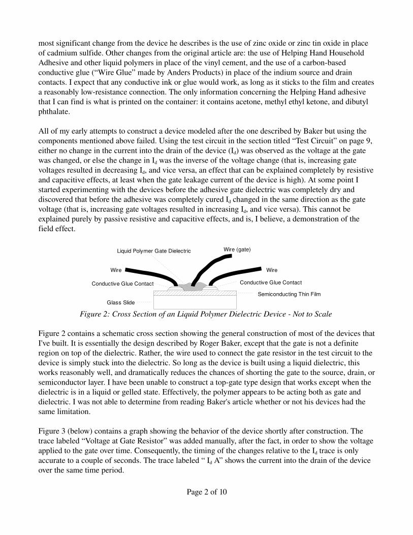
Figure 2 contains a schematic cross section showing the general construction of most of the devices that I've built. It is essentially the design described by Roger Baker, except that the gate is not a definite region on top of the dielectric. Rather, the wire used to connect the gate resistor in the test circuit to the device is simply stuck into the dielectric. So long as the device is built using a liquid dielectric, this works reasonably well, and dramatically reduces the chances of shorting the gate to the source, drain, or semiconductor layer. I have been unable to construct a topgate type design that works except when the dielectric is in a liquid or gelled state. Effectively, the polymer appears to be acting both as gate and dielectric. I was not able to determine from reading Baker's article whether or not his devices had the same limitation.
Figure 3 (below) contains a graph showing the behavior of the device shortly after construction. The trace labeled “Voltage at Gate Resistor” was added manually, after the fact, in order to show the voltage applied to the gate over time. Consequently, the timing of the changes relative to the Id trace is only accurate to a couple of seconds. The trace labeled “ Id A” shows the current into the drain of the device over the same time period.
Page 2 of 10
Figure 2: Cross Section of an Liquid Polymer Dielectric Device Not to Scale
Glass Slide
Semiconducting Thin Film
Conductive Glue ContactConductive Glue Contact
Liquid Polymer Gate Dielectric
Wire
Wire (gate)
Wire
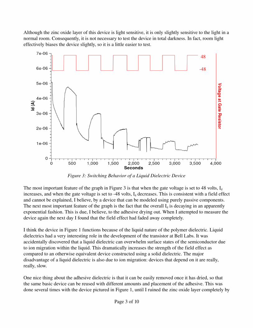
Although the zinc oxide layer of this device is light sensitive, it is only slightly sensitive to the light in a normal room. Consequently, it is not necessary to test the device in total darkness. In fact, room light effectively biases the device slightly, so it is a little easier to test.
The most important feature of the graph in Figure 3 is that when the gate voltage is set to 48 volts, Id
increases, and when the gate voltage is set to 48 volts, Id decreases. This is consistent with a field effect and cannot be explained, I believe, by a device that can be modeled using purely passive components. The next most important feature of the graph is the fact that the overall Id is decaying in an apparently exponential fashion. This is due, I believe, to the adhesive drying out. When I attempted to measure the device again the next day I found that the field effect had faded away completely.
I think the device in Figure 1 functions because of the liquid nature of the polymer dielectric. Liquid dielectrics had a very interesting role in the development of the transistor at Bell Labs. It was accidentally discovered that a liquid dielectric can overwhelm surface states of the semiconductor due to ion migration within the liquid. This dramatically increases the strength of the field effect as compared to an otherwise equivalent device constructed using a solid dielectric. The major disadvantage of a liquid dielectric is also due to ion migration: devices that depend on it are really, really, slow.
One nice thing about the adhesive dielectric is that it can be easily removed once it has dried, so that the same basic device can be reused with different amounts and placement of the adhesive. This was done several times with the device pictured in Figure 1, until I ruined the zinc oxide layer completely by
Page 3 of 10
Figure 3: Switching Behavior of a Liquid Dielectric Device
48
48
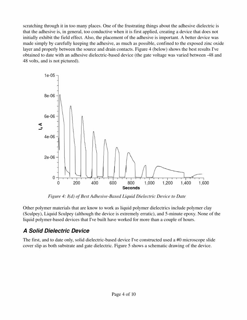
scratching through it in too many places. One of the frustrating things about the adhesive dielectric is that the adhesive is, in general, too conductive when it is first applied, creating a device that does not initially exhibit the field effect. Also, the placement of the adhesive is important. A better device was made simply by carefully keeping the adhesive, as much as possible, confined to the exposed zinc oxide layer and properly between the source and drain contacts. Figure 4 (below) shows the best results I've obtained to date with an adhesive dielectricbased device (the gate voltage was varied between 48 and 48 volts, and is not pictured).
Other polymer materials that are know to work as liquid polymer dielectrics include polymer clay (Sculpey), Liquid Sculpey (although the device is extremely erratic), and 5minute epoxy. None of the liquid polymerbased devices that I've built have worked for more than a couple of hours.
A Solid Dielectric DeviceThe first, and to date only, solid dielectricbased device I've constructed used a #0 microscope slide cover slip as both substrate and gate dielectric. Figure 5 shows a schematic drawing of the device.
Page 4 of 10
Figure 4: I(d) of Best AdhesiveBased Liquid Dielectric Device to Date
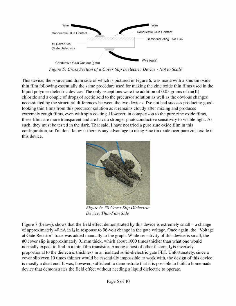
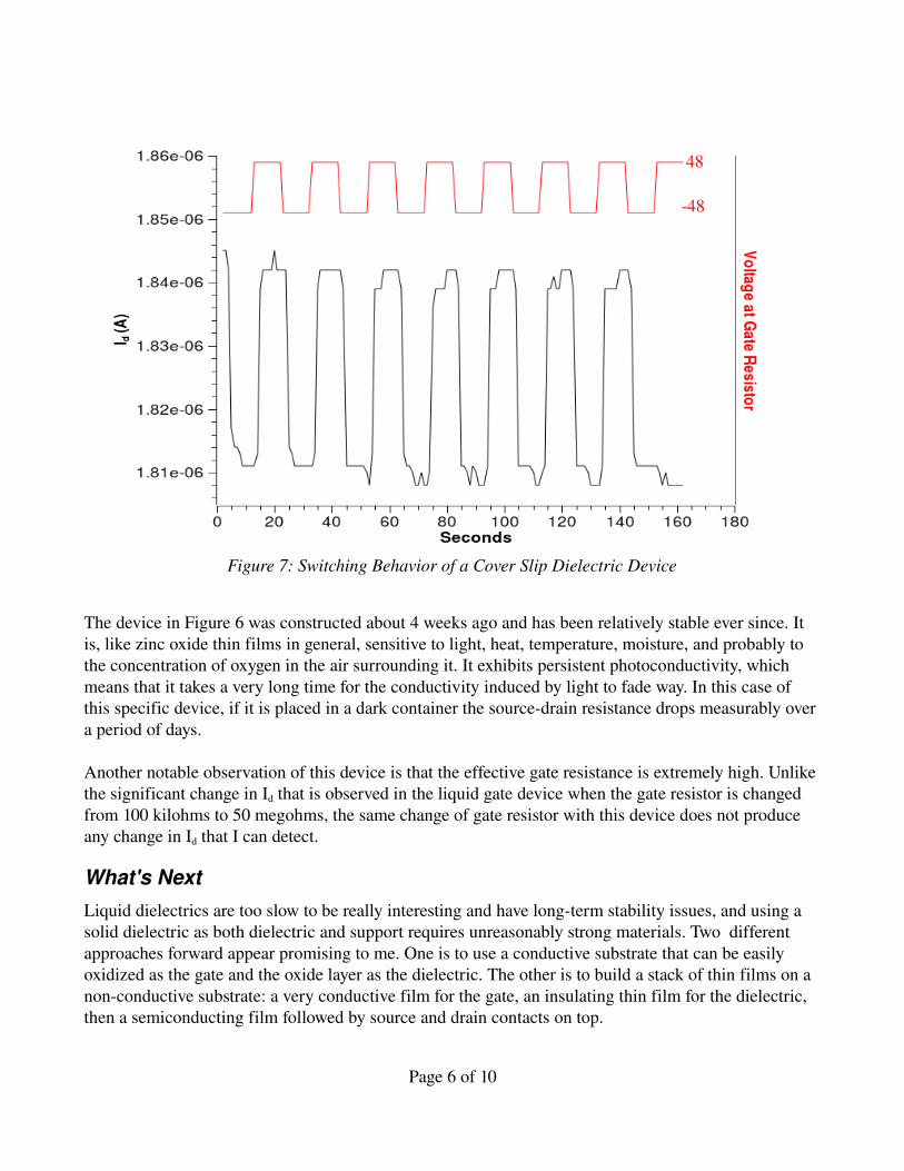
This device, the source and drain side of which is pictured in Figure 6, was made with a zinc tin oxide thin film following essentially the same procedure used for making the zinc oxide thin films used in the liquid polymer dielectric devices. The only exceptions were the addition of 0.05 grams of tin(II) chloride and a couple of drops of acetic acid to the precursor solution as well as the obvious changes necessitated by the structural differences between the two devices. I've not had success producing goodlooking thin films from this precursor solution as it remains cloudy after mixing and produces extremely rough films, even with spin coating. However, in comparison to the pure zinc oxide films, these films are more transparent and are have a stronger photoconductive sensitivity to visible light. As such, they must be tested in the dark. That said, I have not tried a pure zinc oxide film in this configuration, so I'm don't know if there is any advantage to using zinc tin oxide over pure zinc oxide in this device.
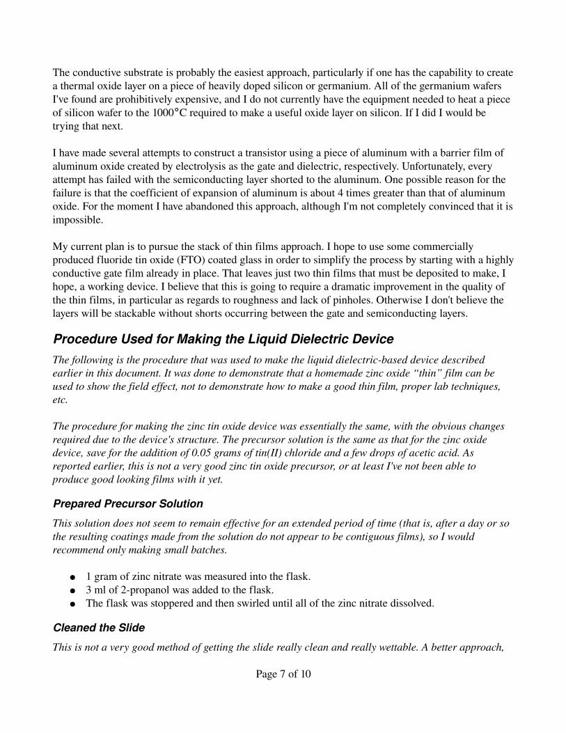
Figure 7 (below), shows that the field effect demonstrated by this device is extremely small – a change of approximately 40 nA in Id in response to 96volt change in the gate voltage. Once again, the “Voltage at Gate Resistor” trace was added manually to the graph. While sensitivity of this device is small, the #0 cover slip is approximately 0.1mm thick, which about 1000 times thicker than what one would normally expect to find in a thinfilm transistor. Among a host of other factors, Id is inversely proportional to the dielectric thickness in an isolated soliddielectric gate FET. Unfortunately, since a cover slip even 10 times thinner would be essentially impossible to work with, the design of this device is mostly a dead end. It was, however, sufficient to demonstrate that it is possible to build a homemade device that demonstrates the field effect without needing a liquid dielectric to operate.
Page 5 of 10
Figure 6: #0 Cover Slip Dielectric Device, ThinFilm Side
Figure 5: Cross Section of a Cover Slip Dielectric Device Not to Scale
#0 Cover Slip(Gate Dielectric)
Semiconducting Thin Film
Conductive Glue Contact
Wire
Wire (gate)
Wire
Conductive Glue Contact
Conductive Glue Contact (gate)
The device in Figure 6 was constructed about 4 weeks ago and has been relatively stable ever since. It is, like zinc oxide thin films in general, sensitive to light, heat, temperature, moisture, and probably to the concentration of oxygen in the air surrounding it. It exhibits persistent photoconductivity, which means that it takes a very long time for the conductivity induced by light to fade way. In this case of this specific device, if it is placed in a dark container the sourcedrain resistance drops measurably over a period of days.
Another notable observation of this device is that the effective gate resistance is extremely high. Unlike the significant change in Id that is observed in the liquid gate device when the gate resistor is changed from 100 kilohms to 50 megohms, the same change of gate resistor with this device does not produce any change in Id that I can detect.
What's NextLiquid dielectrics are too slow to be really interesting and have longterm stability issues, and using a solid dielectric as both dielectric and support requires unreasonably strong materials. Two different approaches forward appear promising to me. One is to use a conductive substrate that can be easily oxidized as the gate and the oxide layer as the dielectric. The other is to build a stack of thin films on a nonconductive substrate: a very conductive film for the gate, an insulating thin film for the dielectric, then a semiconducting film followed by source and drain contacts on top.
Page 6 of 10
Figure 7: Switching Behavior of a Cover Slip Dielectric Device
48
48
The conductive substrate is probably the easiest approach, particularly if one has the capability to create a thermal oxide layer on a piece of heavily doped silicon or germanium. All of the germanium wafers I've found are prohibitively expensive, and I do not currently have the equipment needed to heat a piece of silicon wafer to the 1000°C required to make a useful oxide layer on silicon. If I did I would be trying that next.
I have made several attempts to construct a transistor using a piece of aluminum with a barrier film of aluminum oxide created by electrolysis as the gate and dielectric, respectively. Unfortunately, every attempt has failed with the semiconducting layer shorted to the aluminum. One possible reason for the failure is that the coefficient of expansion of aluminum is about 4 times greater than that of aluminum oxide. For the moment I have abandoned this approach, although I'm not completely convinced that it is impossible.
My current plan is to pursue the stack of thin films approach. I hope to use some commercially produced fluoride tin oxide (FTO) coated glass in order to simplify the process by starting with a highly conductive gate film already in place. That leaves just two thin films that must be deposited to make, I hope, a working device. I believe that this is going to require a dramatic improvement in the quality of the thin films, in particular as regards to roughness and lack of pinholes. Otherwise I don't believe the layers will be stackable without shorts occurring between the gate and semiconducting layers.
Procedure Used for Making the Liquid Dielectric DeviceThe following is the procedure that was used to make the liquid dielectricbased device described earlier in this document. It was done to demonstrate that a homemade zinc oxide “thin” film can be used to show the field effect, not to demonstrate how to make a good thin film, proper lab techniques, etc.
The procedure for making the zinc tin oxide device was essentially the same, with the obvious changes required due to the device's structure. The precursor solution is the same as that for the zinc oxide device, save for the addition of 0.05 grams of tin(II) chloride and a few drops of acetic acid. As reported earlier, this is not a very good zinc tin oxide precursor, or at least I've not been able to produce good looking films with it yet.
Prepared Precursor Solution
This solution does not seem to remain effective for an extended period of time (that is, after a day or so the resulting coatings made from the solution do not appear to be contiguous films), so I would recommend only making small batches.
● 1 gram of zinc nitrate was measured into the flask.● 3 ml of 2propanol was added to the flask.● The flask was stoppered and then swirled until all of the zinc nitrate dissolved.
Cleaned the Slide
This is not a very good method of getting the slide really clean and really wettable. A better approach,
Page 7 of 10
that does not involve harsh chemicals, is to use an aqueous suspension of CeO powder and a paper lap to manually polish the side to be coated in place of the step involving oxalic acid. By the way, once you start cleaning the slide, do touch the surface to be coated with your bare hand.
● The slide was washed with soap and water. ● Several drops of an oxalic acid solution were put on the slide and the surface scrubbed.● The slide was rinsed with distilled water and then with 2propanol.● The slide was dried using a fan.
Coated Slide with Precursor Solution
This method of distributing the solution across the slide is really not a very effective one, particularly if you are attempting to obtain a highquality film. A better method is to use a spin coater. A perfectly functional spin coater can be made from a variablespeed brushless computer fan.
● 5 drops of the zinc nitrate/2propanol precursor solution were placed on the slide. ● The solution was spread over the entire slide using the main body of a plastic pipette.
Baked the Slide
The general method in all of the papers that I have found is to first evaporate the solvent at a much lower temperature before baking the film at a higher temperature. However, assuming the slide does not break and you do not need a particularly high quality film, skipping that step is not fatal to the process.
● The slide was placed in the center of a hot plate that was already at its max temperature of 540C, coated side up.
● After 30 minutes the slide was carefully removed from the hot plate and allowed to cool.
Added Source and Drain Contacts and Wires
The solvent in the conductive glue makes the zinc oxide thin film highly conductive, so measurements taken before the solvent has completely evaporated are generally suspect. However, I don't believe doing so harms the device in any way.
● Several pairs of closely spaced parallel contacts were painted across the short length of the slide using “Wire Glue”.
● The best pair of contacts (that is, the pair with the smallest noncontacting spacing) was chosen and short wires where tacked down using some modeling clay so that one end of each wire rested on one of the chosen contacts. Additional Wire Glue was used to secure the wires to the contacts.
● The slide was left alone for several hours while the wire glue dried.
Verified Operational Film and Contacts
If the resistance of the device does not change significantly when exposed to UV light, the device is most likely not going to show any field effect either. Possible causes are: old precursor solutions, insufficient heating (if the film, assuming a pure zinc oxide film is being made, does not turn white it has not been heated to a high enough temperature or there are contaminants in one of the precursor
Page 8 of 10

ingredients), insufficient cleaning of the slide, contaminants in one of the precursor ingredients.
● Connected an ohmmeter to the two contacts and noted the reading (effectively infinite, according to my meter).
● Pointed the light from a coin celloperated UV flashlight at the device and noted that the reading decreased significantly (however, the reading was not noted long enough to make it into this document).
Adding a Dielectric, a Gate, and Testing
● Verified that both power sources for the test circuit were turned off.● Placed the device on a flat surface near the test circuit and secured the slide to the surface using
a small piece of tape.● Connected the source and drain wires to the test circuit.● Placed a thin wire to be used as the gate such that it was lying horizontally between the source
and drain contacts, but did not actually touch either the source, drain, or thin film. A piece of tape was used to secure the wire in this position without covering any of the wire that was actually above the slide.
● Placed a drop of the Helping Hand Household Adhesive on the device such that it covered the wire gate, source, drain and the film exposed between the source and drain.
● Turned on the power sources for the test circuit, stopped for dinner, returned and started recording data and flipping the switch controlling the polarity of the voltage applied to the gate at 5minute intervals.
Test CircuitFigure 8 illustrates the circuit used to test the devices. Making sense of the reading, particularly when using a liquid dielectric that is constantly in the process of drying (at least until it stops working at all) is much easier if you have have access to equipment that will allow you to automatically record Id over time. I'm using an old Radio Shack device that has an RS232 interface built in and QtDMM to record the values. The meter is somewhat more sensitive to voltage than to current, which is why the meter is set up to read voltages and the data converted to amps after the fact. One does to remember to adjust for the input resistance of the meter in this configuration when doing the conversion from volts to amps.
The gate resistor (RGATE) is used to limit the maximum current in the case of a short, and is also
Page 9 of 10
Figure 8: Test Circuit

useful when attempting to get some idea of the magnitude of the effective resistance of the dielectric. If you can change between a relatively small value (100 kilohm, for example), and a much larger value (50 megohm, for example), without any observable change in the behavior of the device, you can be certain that the effective dielectric resistance is at least 10 times that of the larger resistor.
The 10kilohm resistor connected to the 48volt power supply exists in the circuit as a current limiter. The 030 volt supply does not need one as I am using a bench supply that can be set to a very small current limit.
Page 10 of 10